1
i386-Drive
Chapter 3: Hardware
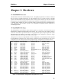
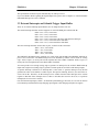
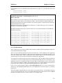
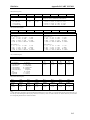
I/O space
Select Signal
Location
Usage
0xa0c0-0xa0cf
0xa0e0-0xa0ef
0xa0f0-0xa0ff
0xb000-0xb0ff
Not mapped
0x????
0x????
0xc000
/CS2
/CS2
/CS2
/CS5
/CS0
/CS1
/CS3
/CS4
J2 pin 5 = P22
J2 pin 5 = P22
J2 pin 5 = P22
None (U9-74HC259)
N/A
J2 pin 37 = P21
J2 pin 10 = P23
J2 pin 3 = P24
/S2 for PPI2
/S4 for SCC2692
/CLR for DAC U09 LTC1450
Internal Usage (T0-T7)
SRAM
16-bit Flash U15
16-bit SRAM, U17 and U18
Read/write 16-bit ADC/DAC
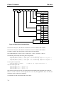
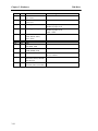
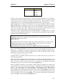
A total of eight pre-decoded chip-select lines are available on the ID. These include the UCS (upper chip
select), and signals CS0-6. The upper chip select is dedicated for boot-up ROM use.
The pre-decoded chip select lines listed in the table above can be used for application, if the on-board
optional corresponding device is not installed.
To use one of the chip select lines, you must map the appropriate line to a free base I/O address. After
configuring the PIO pin appropriately for this peripheral function (normal-mode operation), you can
directly outport to that address with appropriate data. The address bus and data bus should then be
connected to your I/O component if needed.
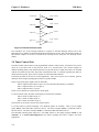
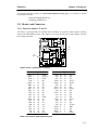
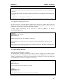
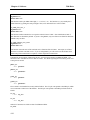
To illustrate how to interface the i386-Drive with external I/O boards, a simple decoding circuit for
interfacing to an external 82C55 I/O chip is shown in Figure 3.2.
82C55
74HC138
A4
A5
A6
1
2
3
/CS6=J1.19
A7
4
5
6
A
B
C
G2A
G2B
G1
Y0
Y1
Y2
Y3
Y4
Y5
Y6
Y7
15
14
13
12
11
10
9
7
RST
SEL8080
/SEL8090
/SEL80A0
/SEL80B0
/SEL80C0
/SEL80D0
/SEL80E0
/SEL80F0
P00-P07
A0/BLE
A1
/SEL8090
/CS
/WR
/WR
/RD
/RD
D0-D7
P10-P17
P20-P27
Figure 3.2 Interface i386-Drive to external I/O devices
The function ie_init() by default initializes the /CS6 line at base I/O address starting at 0x8000. You
can read from the 82C55 with inportb(0x8090) or write to the 82C55 with outportb(0x8090,dat). The
call to inportb will activate /CS6, as well as putting the address 0x8090 over the address bus. The
decoder will select the 82C55 based on address lines A4-6, and the data bus will be used to read the
appropriate data from the off-board component.
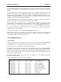
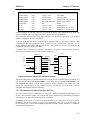
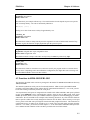
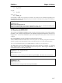
3.9.2 Programmable Peripheral Interface (82C55A)
U02 and U01 PPIs (82C55, or uPD81055L) are low-power CMOS programmable parallel interface units
for use in microcomputer systems. They each provide 24 I/O pins that may be individually programmed
in two groups of 12 and used in three major modes of operation.
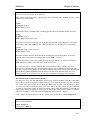
In MODE 0, the two groups of 12 pins can be programmed in sets of 4 and 8 pins to be inputs or outputs.
In MODE 1, each of the two groups of 12 pins can be programmed to have 8 lines of input or output. Of
the 4 remaining pins, 3 are used for handshaking and interrupt control signals. MODE 2 is a strobed bidirectional bus configuration.
3-7