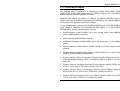
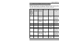
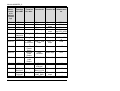
1
Module A9M9750_2 Users Manual Module A9M9750_2 Copyright 2005: FS Forth-Systeme GmbH Postfach 1103, 79200 Breisach, Germany Release of Document: Filename: Author: Program Version April 05, 2005 UM_Module_A9M9750_2.doc Karl Rudolf All rights reserved. No part of this document may be copied or reproduced in any form or by any means without the prior written consent of FS Forth-Systeme GmbH. 2 Module A9M9750_2 1. Revision History 2005-04-05 (V1.00) KR: Initial Version derived from Spec A9M9750_2 Module 3 Module A9M9750_2 Table of Contents 1. Revision History ............................................................................................. 3 2. Introduction .................................................................................................... 6 2.1. Benefits of the ModARM9 Concept ...................................................... 6 2.2. Common Features ............................................................................... 6 2.3. Differences between A9M9750_1 and A9M9750_2 Modules ............... 7 2.4. Planned and realised Variants for A9M9750_2 Module ........................ 8 3. A9M9750 Features......................................................................................... 9 3.1. Size 60 x 44 mm .................................................................................. 9 3.2. 2 x 120-pin connectors ......................................................................... 9 3.3. NS9750 CPU on the A9M9750_2 Module ............................................ 9 3.4. Configuration Pins CPU ..................................................................... 10 3.5. Configuration Pins Module ................................................................. 15 3.6. Clock Generation ............................................................................... 18 3.7. Serial Boot EEPROM, Boot SPI Channel Settings ............................. 21 3.8. Chip Selects, Memory Map ................................................................ 21 3.9. NAND Flash ....................................................................................... 23 3.10.16/32/64 MBytes SDRAM .................................................................. 25 3.11.50 GPIO Pins (multiplexed with other Functions)............................... 27 3.12.PCI/CardBus Port .............................................................................. 30 3.13.10/100Mbps Ethernet Port ................................................................. 31 3.14.USB 2.0 full and low speed Host and Device Controller..................... 31 3.15.UART Channels................................................................................. 31 3.16.SPI Channels..................................................................................... 31 3.17.Calculation of Baudrates.................................................................... 32 3.18.I²C Bus .............................................................................................. 34 3.19.LCD Controller (STN & TFT).............................................................. 36 3.20.Serial EEPROM for storing Configuration Parameters ....................... 36 3.21.RTC................................................................................................... 36 3.22.JTAG, Boundary Scan ....................................................................... 36 3.23.Single 3.3V Power Supply ................................................................. 38 3.24.Power Sequencing on A9M9750_2 Module ....................................... 38 3.25.Voltage Supervision and RESET Generation..................................... 39 4. Bootloader.................................................................................................... 40 4 Module A9M9750_2 5. Software .......................................................................................................40 6. Mechanics ....................................................................................................42 6.1. Extended Module................................................................................44 7. Known Faults and Limitations .......................................................................46 7.1. USB Pins are not 5V tolerant ..............................................................46 7.2. Timing Bug in IIC Stage ......................................................................46 7.3. PLL Clock Generation instable............................................................46 8. Appendix.......................................................................................................47 8.1. Pinning Module ...................................................................................47 8.2. Pinning Module on A9MVali Validation Board .....................................47 8.3. Pinning Module on A9M9750DEV Development Board ......................47 5 Module A9M9750_2 2. Introduction There are now a number of interesting ARM9-based SoC solutions available on the market. These chips are usually designed for particular market segments, which implies a departure from the “one-size-fits-all” philosophy for the modules. To accommodate this, the ModARM9 concept foresees more than one ARM9based module, with the modules having a common subset of functions. One, or two, of these modules will become a standard product at FS Forth, the others will be custom designs. The first standard module, based on the NetSilicon NS9750, is called the A9M9750. The 1st silicon of the NS9750 had a lot of bugs; some of these needed hardware work arounds extending the 1st A9M9750_0 modules size about 8mm on the long side. With the announcement of the 2nd silicon NS9750_A1 most of the important bugs are fixed; all new modules A9M9750_X have the original size of 60X44mm. Due to the fact of PLL instabilities in the 2nd silicon the module A9M9750_2 was necessary with changed generators for system and USB clock. 2.1. Benefits of the ModARM9 Concept One of the problems constantly faced at any design house involved in custom designs is how to re-use the work done in previous designs. The ModARM9 concept is designed to help address this by expanding the common set of tools available to the design engineers. For example, an evaluation board will be designed which is the same for all modules. This will allow the “common features” of a new module to be tested quickly. If the new module is a custom design, then the customer’s base board must be used to test all the peripherals available on the module. This will allow custom designs to be offered at a more attractive price than previously possible. 2.2. Common Features Below are the common features of this module, which will be covered in further detail later in the document. • 6 ARM9 core with MMU Module A9M9750_2 • Size 60mm x 44mm with 240-pin connector • SDRAM 16MB – 256MB • NAND Flash 32MB – 256MB • 2..4 serial RS232 interfaces • Host or device USB interface, USB2.0 compliant • 10/100Mbps Ethernet interface • I²C interface, 100KHz and 400KHz • SPI interfaces • JTAG interface This means that approx. 150 pins of the connector are reserved for the above functionality, the others are free for module-specific functions. 2.3. Differences between A9M9750_1 and A9M9750_2 Modules The NS9750_A1 chips has still an important bug: System frequencies are instable if system and USB clock is generated by crystal circuits. Stable clocks are ensured only when both clocks are made by oscillators. This information was distributed by NetSilicon when the A9M9750_1 redesign was finished. So another redesign was necessary ending in the module A9M9750_2. Differences in detail: 1. System clock 29.4912MHz now made with oscillator 2. USB clock 48MHz now made with oscillator 3. RSTIN# directly connected to U13 pin 7 (MR#). 4. Pull up resistor R34 from RSTIN# to +3.3V added. 7 Module A9M9750_2 2.4. Planned and realised Variants for A9M9750_2 Module Modules using CPU A1 chips with working PLL will have at least two speed and temperature variants: 1. CPU speed 199.0656MHz, 0..70° temperature range. Realised: V01/0364 with 32M NAND Flash and 16M SDRAM, V02/0380 with 32M NAND Flash and 64M SDRAM 2. CPU speed 162.5MHz, -40..+85° temperature range. Not realised in the moment Maybe a PCI host and client version of each variant will be created, which have different parts in the PCI block populated. 8 Module A9M9750_2 3. A9M9750 Features 3.1. Size 60 x 44 mm The A9M9750 module has a size of 60 X 44 mm. 3.2. 2 x 120-pin connectors Two 120-pin connectors on the long side of the module allow accessing most signals of the NetSilicon NS9750 CPU. An optional extension with another two 60-pin connectors is planned. This will extend the length of the module from 60mm to approximately 95mm. Pin-compatible in power supply and main port functions to other ModARM9 modules. 3.3. NS9750 CPU on the A9M9750_2 Module NS9750 CPU has a 32-bit ARM926EJ-S core. Further details see Hardware Reference 9000624c.pdf. NetSilicon has planned to support two temperature ranges: • 0..70°C with 200MHz CPU clock • -40..+85°C with 162.5MHz CPU clock 9 Module A9M9750_2 3.4. Configuration Pins CPU Several pins allow configuration of the CPU before booting. CPU pins have weak pull ups (value range is 15..300K) for a default configuration. Most pins do not have configuration options, some are connected for internal configuration on the module; some others allow external configuration via external connector pins. The configuration state is latched 5 system crystal clock cycles after the rising edge of the PWRGOOD signal at the RESET# input of the CPU (5 * 1 / (29.4912.* 10E6 = 169.5ns) Data Sheet of NS9750 Usage on Module CPU Pin Function PU/PD RTCK PCIAC (PCI Arbiter Configuration) 0 = External PCI Arbiter 1 = Internal PCI Arbiter PD 2k2 optional RESET_D BOOTDS (Boot Mode) 0 = Boot from SPI ONE EEPROM 1 = Boot from Flash/ROM CONF0 CS1LEP (Chip select 1 byte lane enable polarity Bootstrap Select) 0 = BEx# function 1 = WEx# function CONF0 is inverted CONF1 CARDBSEL (CardBus Mode Bootstrap Select) 0 = CardBus mode 1 = PCI mode CONF2 MEMRDSEL (Memory Interface read mode Bootstrap Select) 0 = Command delayed mode 1 = Clock delayed mode CONF4,3 CS1DWSEL (Chip Select 1 10 external configu rable no external Comment pin name no internal PCI arbiter on PCI host version, external PCI arbiter on PCI device version; pin RTCK is not provided on module RSTOUT# Boot mode default from serial SPI EEPROM PD 2k2 no - no no - yes HCONF3 PD 2k2 no no default PCI mode, can be changed externally with pin HCONF3 always command delayed mode, clock delayed mode does not work - no no default 32bit. Set to WEx# function. Not relevant on module. Module A9M9750_2 Data Sheet of NS9750 GPIO2,0 GPIO17,1 2,10,8,4 GPIO19 GPIO24,2 0 GPIO36 GPIO37 GPIO44 Data width bootstrap select) 00 = 16 bits 01 = 8 bits 10 = reserved 11 = 32 bits PLL_FS(1:0) (PLL Frequency divider select) 00 = 4 01 = 8 10 = 1 11 = 2 (default) GPIO2 inverted, GPIO0 not inverted PLL_ND(4:0) (PLL multiplier = ND+1) b11010 = 26 decimal PLL multiplier default 27 GPIO10, 4 inverted PLLBP (PLL bypass) 0 = PLL bypassed 1 = PLL not bypassed GPIO19 is inverted PLL_IS(1:0) (PLL charge pump current ND) 00 = ND0..3 01 = ND4..7 10 = ND8..15 11 = ND16..31 (default) MODVERS0 (LSB Module Version) MODVERS1 (MSB Module Version) GPIO37 GPIO36 0 1 V2.0, CPU PLL ok ENDSEL (Endian mode) 0 = Big endian 1 = Little endian Usage on Module Not relevant on module, as we do always boot from SPI EEPROM no GPIO0 = config. pins on TXDB or module n. c. SPI_DOB, GPIO2 = RTSB# 5 PD 2K2 optional no PD 2k2 optional no GPIO4 = DTRB# GPIO8 = TXDA or SPI_DOA GPIO10 = RTSA# GPIO12 = DTRA# GPIO17 = USB Power Relay GPIO19 = LCDHSY NC - no GPIO20 = pins on module n. LCD_CLK c. GPIO24 = LCDD0 PD 2k2 optional PD 2k2 no GPIO36 = GPIO36 left open LCDD12 GPIO37 = GPIO37 PD LCDD13 PD 2k2 optional no no GPIO44 = resistor not TXDD or populated sets to SPI_DOD little endian. 11 Module A9M9750_2 Data Sheet of NS9750 Usage on Module GPIO44 is inverted GPIO49 CS1POLSEL (Chip select 1 polarity) 0 = Active high 1 = Active low GPIO49 is inverted PU 10k no - SPI Boot does not work in big endian mode (?) Not relevant on module, as we do always boot from SPI EEPROM. Used as FR/B#. PU 10k is at NAND-Flash. 32 of the 50 GPIO pins allow user specific configurations. They are latched in the GEN_ID register with the rising edge of RESET# (address 0xA0900210). Bit GEN_ID GPIO GPIO49 31 30 29 28 27 26 25 24 23 22 21 20 12 GPIO48 GPIO47 GPIO46 GPIO45 GPIO44 GPIO43 GPIO42 GPIO41 GPIO40 GPIO39 GPIO38 GPIO37 GPIO36 GPIO35 GPIO34 GPIO33 GPIO32 GPIO31 GPIO30 Configuratio n usage CS1POLSEL Configuration Protection ENDSEL yes SCONF3 SCONF2 SCONF1 SCONF0 MOD_VER1 MOD_VER0 yes yes yes yes yes yes ext. usage no (NAND FR/B#) DMA1_REQ LCDD23 LCDD22 LCDD21 LCDD20 LCDD19 LCDD18 LCDD17 LCDD16 LCDD15 LCDD14 LCDD13 LCDD12 LCDD11 LCDD10 LCDD9 LCDD8 LCDD7 LCDD6 Module A9M9750_2 Bit GEN_ID GPIO 19 18 17 16 15 GPIO29 GPIO28 GPIO27 GPIO26 GPIO25 GPIO24 GPIO23 GPIO22 14 13 12 10 9 GPIO21 GPIO20 GPIO19 GPIO18 GPIO17 GPIO16 GPIO15 8 GPIO14 7 GPIO13 6 GPIO12 GPIO11 GPIO10 11 5 Configuratio n usage Configuration Protection PLL_IS1 yes PLL_IS0 PLLBP yes yes PLL_ND4 yes PLL_ND3 yes PLL_ND2 yes PLL_ND1 yes PLL_ND0 yes GPIO9 GPIO8 4 GPIO7 3 GPIO6 2 GPIO5 GPIO4 ext. usage LCDD5 LCDD4 LCDD3 LCDD2 LCDD1 LCDD0 LCD_LEND LCD_BIAS_D_ EN LCD_VFSYNC LCD_CLK LCD_HSYNC LCD_PWREN USB_PWRREL USB_OVCUR DCDA#, SPI_ENA# RIA#, SPI_CLKA DSRA# (used as RTC_INT#) DTRA# GPIO11 GPIO10 (RTSA#) RXDA, SPIA_DI TXDA, SPIA_DO DCDB#, SPIB_EN# RIB#, SPIB_CLK DSRB# DTRB# 13 Module A9M9750_2 Bit GEN_ID GPIO 1 0 Configuratio n usage Configuration Protection GPIO3 GPIO2 GPIO1 PLL_FS1 yes GPIO0 PLL_FS0 yes ext. usage CTSB# RTSB# RXDB, SPIB_DI TXDB, SPIB_DO The GPIO configuration pins marked as protected are separated from the external connector pins with an analog switch when RESET# active or their output signal is buffered. So external signal connections cannot change the preset hardware configurations on the module or external configuration pins. The switched port lines have 10K pull ups when open to prevent floating. signals. Switching time at the rising edge of PWRGOOD is delayed about 200ns (configuration is latched 5 system crystal clock cycles after the rising edge of PWRGOOD in the CPU). Using not protected pins for configuration purposes is possible, if the major load is the configuration resistor. RTCK is not connected to external and has no switching logic. RSTOUT# is generated from RESET_DONE & PWRGOOD. So RESET_DONE cannot be loaded externally. Another three configuration pins on the CPU are used for internal tests from NetSilicon and to switch from normal mode to ARM/JTAG debug or boundary scan mode. Switching is done with the configuration pins DEBUG_EN# and OCD_EN# described in the next chapter. PLLTST# (AF21) 1 1 1 14 BISTEN# (AD20) 0 1 0 SCANEN# (AE21) 0 0 0 Mode normal Debug enable Boundary Scan enable Module A9M9750_2 3.5. Configuration Pins Module Module configuration pins change either hardware configurations on the module (HCONF0..3) or they are user specific and can be read in the GEN_ID register (SCONF0..3). Signal name DEBUG_EN# FWP# OCD_EN# Function PU/ PD PU 10K CPU Mode Select 0 = Disconnects TRST# and PWRGOOD for JTAG and Boundary scandebug mode 1 = TRST# and PWRGOOD connected for normal mode (default) internal NAND flash write PU 10K protect 0 = write protect active 1 = no write protect JTAG / Boundary Scan PU 10K function selection 0 = ARM Debug Mode, BISTEN# set to high 1 = Boundary Scan Mode, BISTEN# set to low (default) external pin name Comment HCONF0 HCONF1 HCONF2 Select JTAG mode, DEBUG_EN# has to be low too default PCI mode, can be changed externally with pin HCONF3 CONF1 CARDBSEL (CardBus Mode Bootstrap Select) 0 = CardBus mode 1 = PCI mode HCONF3 GPIO38 User defined software configuration pin, can be read in GEN ID register bit 28, default high User defined software configuration pin, can be read in GEN ID register bit 29, default high User defined software configuration pin, can be SCONF0 read Bit 28 GEN_ID SCONF1 read Bit 29 GEN_ID SCONF2 read Bit 30 GEN_ID GPIO39 GPIO40 15 Module A9M9750_2 Signal name GPIO41 16 Function read in GEN ID register bit 30, default high User defined software configuration pin, can be read in GEN ID register bit 31, default high PU/ PD external pin name SCONF3 Comment read Bit 31 GEN_ID Module A9M9750_2 Recommended Combinations of DEBUG_EN# and OCD_EN#: HCONF0 HCONF2 Mode Comments OFF OFF Normal mode ok ON OFF Debug mode ok OFF ON not recommended, may hang avoid ON ON OCD mode ok 17 Module A9M9750_2 3.6. Clock Generation Different clocks will have to be generated for the module in the CPU: 1. Input clock at X1 (C8) 29.4912 MHz with PLL multiplied to 398.1312 MHz (*27 /2). 2. CPU clock 199.0656 MHz (or 162.5 or 125 MHz depending on CPU version). Multiplied input clock divided by 2. These frequencies are the default values set by strapping pins. PLL Multiplier and divider vaues can be changed at runtime by software; a 4ms RESET allows PLL to lock, usage needs cold/warmstart detection in the software. 3. AHB clock 99.5328 MHz (81.25, 62.5 MHz). Multiplied input clock divided by 4. 4. BBUS clock 49.7664 MHz (40.625, 31.25 MHz). Multiplied input clock divided by 8. 5. PCI clock internally is fixed to input clock divided by 14, (14, 12, 10 or 8 are strapping options). For other frequencies an external clock source connected to PCI_CLK_IN (AB24) has to be used. 6. LCD clock by either dividing input clock (by 4, 8, 16, or 32) or using an external clock source connected to LCDCLOCK (J2). 7. External clock CLKOUT. NS9750 has no dedicated external clock pin. CLKOUT3 from the memory controller is used to generate an external clock of half CPU clock (99.5328MHz or 81.25MHz or 62.5MHz). This clock is buffered with a clock buffer with 4ns slew rates allowing up to 50mA output currents @ 3.3V. Oscillators, PLL settings and resulting frequencies: Unit Oscillator PLL_ND(4:0), PLL Multiplier 18 MHz - Modules with 200MHz CPU (0..70°) 29,4912 0b11111, 27 Modules with 162.5MHz CPU (-40..+85°): 29,4912 0b10000, 22 Module A9M9750_2 Unit PLL_FS(1:0), PLL divider PLL_IS(1:0), value VCO output (= Oscillator * PLL Multiplier) resulting PLL clock (= VCO / PLL Divider) CPU clock (= PLL /2) AHB, SDRAM and external clock (= CPU /2) BBUS clock (= AHB /2) UART Baud Rate Clock X1_SYS_CLK/M internal PCI clock MHz Modules with Modules with 200MHz CPU 162.5MHz CPU (0..70°) (-40..+85°): 0b11, 2 0b11, 2 0b11, ND16..31 0b11, ND16..31 796,2624 648,8064 MHz 398,1312 324,4032 MHz MHz 199,0656 99,5328 162,2016 81,1008 MHz MHz 49,7664 14,4560 40,5504 14,4560 MHz 28,4379 32,4403 19 Module A9M9750_2 Summary Clock Frequencies on Module: Oscillator 29.4912MHz PLL_ND(4:0), PLL Multiplier 11111, 27, CPU PLL active PLL_FS(1:0), PLL divider 11, 2, CPU PLL active PLL_IS(1:0), value 11, ND16..31, CPU PLL active resulting PLL clock 398.1312 CPU clock 199.0656 AHB, SDRAM and external clock 99.5328 BBUS clock 49.7664 UART Baud Rate Clock BBus 49.7664 PCI clock 33.33MHz with external oscillator LCD clock 99.5328MHz, 49.7668MHz, 24,8834MHz or 12,4417MHz SDRAM_CLKOUT0 feeds the SDRAM. A 2nd signal path with the same length as the connection between CPU and SDRAM is coupled to the feedback input SDRAM_CLKIN0. SDM_CLKOUT0 and SDM_CLKIN0 are decoupled with a 22R resistor each. The feedback inputs SDRAM_CLK1..3 are grounded. 20 Module A9M9750_2 3.7. Serial Boot EEPROM, Boot SPI Channel Settings Connected to SPI channel B (GPIO0->SI, GPIO1-> SO, GPIO6->SCK, GPIO7>CS#) is a serial SPI EEPROM 8Kx8 containing initialization values and boot program. It is loaded after end of RESET# low into the SDRAM, if configuration line RESET_DONE is pulled low at the rising edge of RESET# (default on module). The module has to be in little endian mode; a CPU bug prevents booting via SPI EEPROM in big endian mode. To allow external usage of the SPI channel after boot the SPI chip select is divided into an internal and an external SPI chip select. Activation internal chip select SPIB_INT# while RESET_DONE low; activation external chip select SPI_ENB# with RESET_DONE high. 3.8. Chip Selects, Memory Map NS9750 CPU provides 8 chip selects divided in 4 channels for dynamic RAMs and 4 static chip selects. Every chip select has a 256MB range. Below the whole memory map of the NS9750 chip: Name Pin Address Range Size [Mbyte] SDM_CS0# E1 0x00000000..0x0FFFFFFF 256 SDM_CS1# SDM_CS2# SDM_CS3# EXT_CS0# F2 G3 F1 B10 0x10000000..0x1FFFFFFF 0x20000000..0x2FFFFFFF 0x30000000..0x3FFFFFFF 0x40000000..0x4FFFFFFF 256 256 256 256 EXT_CS1# C10 0x50000000..0x5FFFFFFF 256 EXT_CS2# B9 0x60000000..0x6FFFFFFF 256 EXT_CS3# C9 0x70000000..0x7FFFFFFF 256 PCI - 0x80000000..0x8FFFFFFF 256 BBus - 0x90000000..0x9FFFFFFF 256 Usage Comments SDRAM bank 0 n. c. n. c. n. c. external, CS0# NANDFlash external, CS2# external, CS3# PCI memory BBus memory 1 bank on module st Program Memory 21 Module A9M9750_2 PCI PCI - 0xA0000000..0xA00FFFFF 0xA0100000..0xA01FFFFF 1 1 PCI - 0xA0200000..0xA02FFFFF 1 PCI - 0xA0300000..0xA03FFFFF 1 Bridge - 0xA0400000..0xA04FFFFF 1 reserved Ethernet - 0xA0500000..0xA05FFFFF 0xA0600000..0xA06FFFFF 1 Memory - 0xA0700000..0xA07FFFFF 1 LCD - 0xA0800000..0xA08FFFFF 1 System - 0xA0900000..0xA09FFFFF 1 reserved - 0XA0A00000..0xFFFFFFFF 1536 22 PCI IO PCI Configur ation Address PCI Configur ation Data PCI Arbiter BBus to AHB Bridge reserved Ethernet Commun ication Module Memory Controlle r LCD Controlle r System Control Module reserved Module A9M9750_2 3.9. NAND Flash A9M9750 has 32Mx8, 64Mx8 or 128Mx8 NAND Flash onboard. Optionally greater sizes can be populated (depending on availability). The NS9750 does limit the address range of a single chip select to 256MByte, but this is not relevant for NAND Flash, as the interface to the NAND flash needs always 32 kByte here due to usage of A13, 14 for address and command control. The NAND flash is accessed with EXT_CS1#. The chip can be write protected externally with the signal FWP#. Timing considerations (assumes 99.5328MHz AHB and 49.7664MHz BBus clock): Static memory controller has a clock of 99.5328MHz = 10.048ns per clock cycle. The AHB memory controller needs 5 cycles (50ns) for every sequence from start to the activation of the memories address, data and control signals. This timing overhead occurs once per single operation and when running burst cycles. The read or write cycle has a minimum time of one cycle (10ns). The static memory controller allows different adjustments for the memory timings: Values in the registers of static CS1 (verified with module w 199MHz CPU clock), HCLK = 99.5328MHz = 10.048ns per cycle: Chip Select 1 Configuration MEM_StConfig1: 0x80 = no write protect, write buffer disabled, extended wait disabled, BEx# used, chip select low active, bus width 8bit Write Enable Delay MEM_StWaitWen1: 0x1 = 2 HCLK cycles; CS setup is 0ns Output Enable Delay MEM_StWaitOen1: 0x3 = 3 HCLK cycles; data setup is 20ns Length OE in non page mode, Delay 1st read in page mode 23 Module A9M9750_2 MEM_StWaitRd1: 0x8 = 9 HCLK cycles; OE width is 60ns. Important: Length OE is value from this register minus value in MEM_StWaitOen Delay next read in page mode MEM_StWaitpage1: 0x6 = 8 HCLK cycles; data rate is 50ns Delay write MEM_StWaitWr1: 0x5 = 6 HCLK cycles; min write length is 45ns Delay between data direction change MEM_StWaitTurn1: 0x7 = 7 HCLK cycles; delay between WE high and RD low is 60ns 24 Module A9M9750_2 3.10. 16/32/64 MBytes SDRAM One SDRAM bank is available. It is connected to CS4# (SDM_CS0#). CS5# (SDM_CS1#), CS6# (SDM_CS2#) and CS7# (SDM_CS3#) are lost. The module does not provide external SDRAM connection. A9M9750 has 4MX32 (16 MByte) or 16MX32 (64 MByte) SDRAM onboard. Larger chips can be populated (depending on availability), the highest address connected is A12. Range of chip select is 256M. Timing considerations (assumes 99.5328MHz SDRAM and 49.7664MHz BBus clock, usage of 1MX32X4 75ns SDRAM with CAS latency of 2 and 100MHz SDRAM clock). Recommended register settings: 1. Control Register (0xA070 0000): set to 0x1 (normal mode, reset address mirror, enable memory controller) 2. Status Register (0xA070 0004): read only 3. Configuration Register (0xA070 0008): set to 0x0 (clock ratio 1:1, little endian mode) 4. Dynamic Memory Control Register (0xA070 0020): set to 0x3, memory clock enabled 5. Dynamic Memory Refresh Timer register (0xA070 0024): set to 0x63 (16µs refresh time with 100MHz SDRAM clock 6. Dynamic Memory Read Configuration Register (0xA070 0028): set to 0x1, command delayed strategy, clock not delayed (modify only Bit0,1; min 0x1, max 0x3) 7. Dynamic Memory Precharge Command Period Register (0xA070 0030): set to 0x1 = 2 clock cycles; TRP=20ns, (modify only bit0:3) 8. Dynamic Memory Active to Precharge Command Period Register (0xA070 0034): set to 0x4 = 5 clock cycles; TRAS=45ns, (modify only bit0:3) 9. Dynamic Memory Self-refresh Exit Time Register (0xA070 0038): set to 0xF = 0x10 clock cycles; TSREX=???, (modify only bit0:3) 25 Module A9M9750_2 10. Dynamic Memory Last Data Out to Active Time Register (0xA070 003C): set to 0x1 = 2 clock cycles; TAPR=???ns (modify only bit0:3) 11. Dynamic Memory Last Data In to Active Command Time Register (0xA070 0040): set to 0x5 = 6 clock cycles; TDAL or TAPW=40ns, (modify only bit0:3) 12. Dynamic Memory Write Recovery Time Register (0xA070 0044): set to 0x0 = 1 clock cycle; TWR or TDPL or TRWL or TAPW=10ns, (modify only bit0:3) 13. Dynamic Memory Active to Active Command Period Register (0xA070 0048): set to 0x6 = 7 clock cycles; TRC=65ns, (modify only bit0:3) 14. Dynamic Memory Auto Refresh Period Register (0xA070 004C): set to 0x6 = 7 clock cycles; TRFC=???ns, (modify only bit0:4) 15. Dynamic Memory Exit Self-refresh Register (0xA070 0050): set to 0x1F = 0x20 clock cycles; TXSR=???, (modify only bit0:4) 16. Dynamic Memory Active Bank A to Active Bank B Time Register (0xA070 0054): set to 0x1 = 2 clock cycles; TRRD=15ns, (modify only bit0:3) 17. Dynamic Memory Load Mode Register to Active Command Register (0xA070 0058): set to 0x1 = 2 clock cycles; TMRD=???ns, (modify only bit0:3) 18. Dynamic Memory Configuration 0 Register ((0xA070 0100): set for 1MX32X4 to 0x00084500 = buffers enabled, 32-bit extended bus high performance address mapping, 128Mb (4MX32), 4 banks, 12 rows, 8 columns, (modify only bits 20, 14, 12:07) 19. Dynamic Memory RAS and CAS Delay 0 Register (0xA070 104): set to 0x203 = 3 RAS, 2CAS; (modify only bits 0:1 (RAS) and 8:9 (CAS)) 20. System Control Dynamic Memory Base Register 4 (0xA090 01D0): set to 0x00000000 = Start Adress 0; (modify only bits31:12) 21. System Control Dynamic Memory Mask Register 4 (0xA090 01D4): set to 0xF0000000 = Range 256MByte (0x00000000 - 0x0FFFFFFF); (modify only bits31:12) 26 Module A9M9750_2 3.11. 50 GPIO Pins (multiplexed with other Functions) NS9750 has 50 GPIO pins. All pins are multiplexed with other functions (UART, SPI, USB, DMA, parallel port IEEE1284, LCD port, timers, interrupt inputs). Using a pin as GPIO means always to give up another functionality. Port Name, Functio n 03 (default at power up) Alternate Function 00, UART Alternate Function 00, misc. Alternate Alternate On Module Function 01 Function 02 default used as GPIO0 TXDB SPI_Boot_ DO and SPIB_DO DMA0 DONE dupe Timer 1 dupe GPIO1 RXDB SPI_Boot_ DI and SPIB_DI DMA0 REQ. Dupe IRQ0 GPIO2 GPIO3 GPIO4 RTSB# CTSB# DTRB# GPIO5 GPIO6 DSRB# RIB#, RXCLKB GPIO7 DCDB#, TXCLKB GPIO8 GPIO9 TXDA RXDA Timer 0 1284 ACK 1284 BUSY TXDB, SPI_Boot_DO or external SPIB_DO RXDB, SPI_Boot_DI or external SPIB_SI RTSB#, DMA CTSB#, DMA DTRB# DMA1 ACK DMA0 REQ DMA0 DONE 1284 ERR DMA0 ACK DSRB#, DMA SPI_Boot_ 1284 P_JAM Timer 7 RIB#, CLK and dupe SPI_Boot_CL SPIB_CLK K or external SPIB_CLK SPI Boot DMA0 Ack IRQ1 DCDB#, CE# and dupe SPI_Boot_CE SPIB_CE# # or external SPIB_CE# SPIA_DO Reserved Reserved TXDA, SPI A SPIA_ DI Reserved Timer 8 RXDA, SPI A dupe 27 Module A9M9750_2 Port Name, Functio n 03 (default at power up) Alternate Function 00, UART GPIO10 GPIO11 RTSA# CTSA# Reserved IRQ2 dupe GPIO12 GPIO13 DTRA# DSRA# Reserved IRQ0 dupe GPIO14 RIA#, RXCLKA DCDA#, TXCLKA GPIO15 GPIO16 GPIO17 GPIO18 GPIO19 GPIO20 GPIO21 DTRC# DSRC# GPIO22 RIC#, RXCLKC DCDC#, TXCLKC DTRD# GPIO23 GPIO24 28 Alternate Function 00, misc. Alternate Alternate On Module Function 01 Function 02 default used as SPIA_CLK Timer 1 Reserved Timer 0 dupe Reserved Timer 10 dupe Reserved SPIA_EN# Timer 2 Timer 2 USB 1284 P_JAM Overcurren dupe t USB Reserved Power Relay Ethernet LCD CAM PWREN Reject Ethernet LCD HSYNC CAM Reject LCD CLK LCD VFSYNC SPIC_CLK LCD BIAS_D_EN SPIC_ EN# LCD LINE_END LCDD0 Timer 11 dupe RTSA# CTSA# GPIO12 GPIO13, used as RTC_INT# RIA#, SPI A DCDA#, SPI A USB Reserved USB IRQ3 dupe LCD DMA1 ACK LCD Reserved Reserved LCD LCD Reserved LCD Timer 14 dupe Reserved LCD LCD Module A9M9750_2 Port Name, Functio n 03 (default at power up) Alternate Function 00, UART GPIO25 DSRD# GPIO26 RID#, RXCLKD DCDD#, TXCLKD Alternate Function 00, misc. Alternate Alternate On Module Function 01 Function 02 default used as SPID_CLK LCDD2 Timer 15 dupe Timer 3 SPID_ EN# LCDD3 Timer 4 LCD LCDD4 LCDD8 dupe LCD GPIO29 GPIO30 Ext IRQ 1 dupe Timer 5 Timer 6 LCDD5 LCDD6 LCD LCD GPIO31 Timer 7 LCDD7 GPIO32 GPIO33 GPIO34 GPIO35 GPIO36 GPIO37 GPIO38 GPIO39 GPIO40 GPIO41 GPIO42 GPIO43 GPIO44 EXT IRQ 2 Timer 8 Timer 9 Timer 10 Reserved Reserved Reserved Reserved TXDC RXDC RTSC# CTSC# TXDD LCD LCD LCD LCD LCD LCD LCD LCD LCD LCD LCD LCD LCD GPIO45 GPIO46 RXDD RTSD# 1284 D0 1284 D1 1284 D2 1284 D3 1284 D4 1284 D5 1284 D6 1284 D7 IRQ3 Timer 11 Timer 12 Timer 13 1284 PER_ONLIN E 1284 STRB 1284 ALFD LCDD9 dupe LCDD10 dupe LCDD11 dupe LCDD8 LCDD9 LCDD10 LCDD11 LCDD12 LCDD13 LCDD14 LCDD15 LCDD16 LCDD17 LCDD18 LCDD19 LCDD20 LCDD21 LCDD22 LCD LCD GPIO27 GPIO28 LCDD1 LCD LCD LCD 29 Module A9M9750_2 Port Name, Functio n 03 (default at power up) Alternate Function 00, UART GPIO47 GPIO48 GPIO49 CTSD# Alternate Function 00, misc. Alternate Alternate On Module Function 01 Function 02 default used as Timer 14 Timer 15 1284 INIT 1284 P_SEL 1284 P_LOG LCDD23 DMA1 REQ DMA1 DONE LCD DMA R/B# NANDFlash 3.12. PCI/CardBus Port All address, data and control signals are provided to connect a PCI or CardBus interface compliant to PCI specification 2.1 and 2.2 protocol. All module signals are not buffered; clock buffering, clock distribution and casually necessary buffers for other PCI signals have to be added on the application board. If no internal PCI clock is used, the PCI clock has to be generated externally too. PCI_CLKIN and PCI_CLKOUT have series resistors populated with 0R in the moment between CPU and connector; these two signals can be shorted near the CPU optionally on the module. Generation PCI clock see clock chapter. Pull up resistors on the module are provided for PCI_GNT1..3#, PCI_REQ1..3#, PCI_INTA..D#, PCI_PERR#, PCI_SERR#, PCI_STOP#, PCI_DEVSEL#, PCI_IRDY#, PCI_TRDY# and PCI_FRAME#. PCI_CENTRAL_RSC# pin is default low (internal pull down), the internal PCI resources and the internal PCI arbiter of the NS9750 active (RTCK high). This is the PCI host version. PCI_IDSEL is connected via series resistor on the module to PCI_AD11 (NS9750 must be PCI device0). The PCI_IDSEL line of an external PCI Connector has to be connected to PCI_AD signal >11 (for example, connected to PCI_AD13 the connector is configured as PCI device 2). 30 Module A9M9750_2 If external arbiter and no internal resources selected (PCI_CENTRAL_RSC# high and RTCK low), no pull up resistors are populated (PCI device version). PCI_IDSEL is controlled by the external host, the series resistor on the module not populated. 3.13. 10/100Mbps Ethernet Port The module has a MII PHY chip on board. Adress selection is set to 1. The transmit signals TPOP and TPON from the PHY are neither decoupled nor terminated on the module. The receive signals TPIP and TPIN are capacitively coupled with 220pF to the PHY. They have an AC-termination to Gnd with 49R9 from each signal. AC coupling with 100nF to Gnd. Signals for link and speed LEDs are provided. No transformer, Ethernet connector or indication LEDs are on the module, these parts have to be provided by the base board. PHY clock of 25MHz is generated in the PHY chip with a 25MHz crystal. 3.14. USB 2.0 full and low speed Host and Device Controller The USB section of the NS9750 CPU provides USB+ and USB- signals and two USB control signals (USB_PWR and USB_OVCURR). All external configuration for a USB device or a USB host interface has to be made on the base board. 48MHz USB clock is generated on the module with a 48MHz crystal in fundamental configuration. 3.15. UART Channels Up to 4 UART channels with all handshake signals are provided (channels A=GPIO8..15, B=GPIO0..7, C=GPIO20..23 & GPIO40..43, D=GPIO24..27 & GPIO44..47). They can be used in asynchronous mode as UART. Baud rates are supported up to 1.8MHz in asynchronous mode. 3.16. SPI Channels SPI channel B (GPIO0,1,6,7) is connected to the serial 8Kx8 SPI EEPROM U23 when RSTOUT# asserted. The EEPROM contains the boot program and the initial SDRAM parameters for booting via SPI. Usage of this channel at runtime is provided by deconnecting the boot EEPROM with the deassertion of RSTOUT# 31 Module A9M9750_2 using 4 switches. The other SPI channels can be used free if not used in UART mode or blocked by other GPIO usage. 3.17. Calculation of Baudrates Baud rate generators in the NS9750 have different clock sources selectable: 1. X1_SYS_OSC/M. It is the frequency of the input crystal divided by M. M depends on the multiplier settings PLL_ND of the PLL. M = 2 at PLL_ND >=19 decimal (14.7456MHz with 29.4912MHz crystal) or M = 4 at PLL_ND < 19 decimal (7.3728MHz). Cannot be used with PLL bypassed. 2. BCLK. For 199.0656MHz CPU is BCLK = 49.7668MHz. Only internal source when PLL bypassed. 3. External receive clock from GPIO pins. 4. External transmit clock from GPIO pins. These values can be the same for modules with and without used CPU PLL, when BBus is used as clock source. UM = UART mode, either 8, 16, 32. Normally 16 taken. M = input clock divider, 2 for ND > 19 0 <= N <= 16383 decimal for baud rate generator count General calculation formula divider N for clock source 1: N = ((X1_SYS_OSC / M) / (UM * Baudrate)) – 1 simplifies for X1_SYS_OSC/2 = 14.7456MHz to N = (921600 / Baudrate) – 1 and for X1_SYS_OSC/4 = 7.3728MHz to 32 Module A9M9750_2 N = (460800 / Baudrate) – 1 Example for 38400 Bd: N = (460800/38400) – 1 = 11, error 0% General calculation formula divider N for clock source 2: N = (BCLK / (UM * Baudrate)) - 1 simplifies for 49.7664MHz to N = (3110400 / Baudrate) – 1 Example for 38400 Bd: N = (3110400/38400) – 1 = 80, error 0% Simplifies for 40.5504MHz to N = (2,534400 / Baudrate) – 1 Example for 38400Bd N = (2.534400 / 38400) – 1 = 65, error 0% 33 Module A9M9750_2 Count values vs. Baud Rate Clock: Baud Rate 75 150 300 600 1200 2400 4800 7200 9600 14400 19200 28800 38400 57600 115200 230400 460800 921600 1843200 N, X1_SYS/2 = N, X1_SYS/4 N, BBus = 14.7456MHz, = 7.3728MHz, 49.7664MHz, (Error) [%] (Error) [%] (Error), [%] 12287, (-) 6143, (-) 3071, (-) 1535, (-) 767, (-) 383, (-) 191, (-) 127, (-) 95, (-) 63, (-) 47, (-) 31, (-) 23, (-) 15, (-) 7, (-) 3, (-) 1, (-) 0, (-) - 6143, (-) 3071, (-) 1535, (-) 767, (-) 383, (-) 191, (-) 95, (-) 63, (-) 47, (-) 31, (-) 23, (-) 15, (-) 11, (-) 7, (-) 3, (-) 1, (-) 0, (-) - 10367, (-) 5183, (-) 2591, (-) 1295, (-) 647, (-) 431, (-) 323, (-) 215, (-) 161, (-) 107, (-) 80, (-) 53, (-) 26, (-) 13, (+3.846) 6, (-3.846) - N, BBus = 40.5504MHz, (Error) [%] 8447, (-) 4223, (-) 2111, (-) 1055, (-) 527, (-) 353, (+0.18) 263, (-) 176, (+0.18) 131, (-) 87, (+0.749) 65, (-) 43, (+0.749) 21 10 5, (+10.824) CPUs using PLL on modules with 200MHz and 162.5MHz will use the values from column 1 allowing baud rates from 75..921600Bd. A 125MHz CPU will have a PLL multiplier ND = 17 resulting in a X1_SYS/4 clock source. This module will use column 2 resulting in a baud rate from 75..460800Bd. Column 3 or 4 is used when PLL bypassed or CPU clock never changes in the application. 3.18. I²C Bus 34 Module A9M9750_2 This bus (SCL, SDA) is connected on the module to a serial EEPROM with I²C interface on device address 0xA0, 0xA1. Device address 0xD0, 0xD1 connects to an RTC on board. All other addresses can be used externally. Due to a timing bug in the I²C state machine the maximum clock frequency in slow mode should be 50KHz and 200KHz in fast mode. Otherwise minimum setup time for the target can be violated (SDA changes after half low time of SCK instead of shortly after falling edge, so setup time for data is 2.5µs @ 100KHz and 612.5ns @ 400KHz). Important: Use only 3.3V devices! 35 Module A9M9750_2 3.19. LCD Controller (STN & TFT) An LCD interface for STN or TFT LCD’s is provided with up to 24 data lines and 6 control lines. Usage for LCD disables serial ports C, D and most GPIOs. The module provides the full LCD interface: 24 data lines LCCD0..23 (GPIO24..47) and 6 control lines GPIO18..23. This interface allows connection of most TFT and STN monchrome and color LCDs. Details see NS9750 hardware user manual. 3.20. Serial EEPROM for storing Configuration Parameters The nonvolatile storage of parameters like MAC address etc. is supported with a serial 8Kx8 EEPROM (24LC64 or similar) connected to the I²C bus at device address 0xA0, 0xA1. 3.21. RTC An RTC (MAXIM/DALLAS DS1337 in µSOP8 case) on the module is connected to the I²C bus (device address 0xD0, 0xD1). It has its own 32.768KHz clock crystal. Power is taken from 3.3V when provided, otherwise from VRTC fed by an external battery. An interrupt line (GPIO13) is connected to the RTC; it can be opened by depopulating a resistor. 3.22. JTAG, Boundary Scan NS9750 support JTAG and boundary scan with the signals TCK, TMS, TDI, TDO and TRST#. The signal RTCK is not connected to external. It is only used on the module for PCI arbiter selection. Selection between normal mode and debug mode is done with the external signal DEBUG_EN# (HCONF0). Selection between ARM debug mode and boundary scan mode is done with the signal OCD_EN# (HCONF2). See table below: 36 DEBUG_EN# OCD_EN# Mode 1 1 normal Comments Module A9M9750_2 DEBUG_EN# OCD_EN# Mode Comments 1 0 not recommended Boundary Scan possible here too, but TRST# is connected with SRST#, system may hang 0 0 1 0 ARM debug Boundary Scan 37 Module A9M9750_2 3.23. Single 3.3V Power Supply The module has 3.3V_IN supply pins. VLIO pins are connected to 3.3V_IN too for the A9M9750_2 module. These signals have EMI filters near the connector to suppress emission of the module. Internal voltages: 1.5V core voltage with up to 700mA will be converted by a switching regulator to keep losses small. This regulator is connected to VLIO. Worst case power consumption of the NS9750 is at full operation with 200MHz clock 1.05W for the core (1.5V, about 700mA) and 0.65W for the I/O ring (3.3V, about 200mA). In “sleep mode” power consumption decreases to 170..350mW (120..240mA) for the core and 10..90mW (3..30mA) for the I/O ring depending on the ports used for wake up. 3.24. Power Sequencing on A9M9750_2 Module Power-up and power-down behavior recommended by NetSilicon and TOSHIBA for the NS9750 (Power up: core voltage will be first to rise; I/O voltage +3.3V will ramp up in <100ms, when core voltage rises over 80% of its nominal value; Power down: I/O voltage will ramp down in < 100ms, when core voltage falls below 80%) will be ensured by hardware. The sequencing circuit is realised with two comparators, a variable delay and a FET switch TPS2022 U18 between 3.3V_IN and +3.3V on the module. The 1st comparator TLV3012 U12 with a 3.0V threshold supervizes 3.3V_IN. Its output becomes true, if 3.3V_IN > 3.0V. The 2nd comparator TLC7701 U16 supervizes +1.5V core voltage. When +1.5V core voltage > 1.3V, the output becomes true. If both signals are true a delay of about 20..40ms starts. Delay time is settable with a capacitor at U15. After this time output RES goes low and 3.3V_IN are connected to +3.3V with the FET switch U18 with a ramp up time of < 20ms. Output RES# goes high; it is connected as PWREN to the external connector of the module. The outputs of U16 change their state immediately, when either 3.3V_IN < 3.0V or +1.5V < 1.2V. So the +3.3V on the module is switched off immediately and ramps down in a few ms. 38 Module A9M9750_2 3.25. Voltage Supervision and RESET Generation Voltage supervision and RESET# generation is done for 1.5V core and 3.3V I/O voltage by a triple voltage supervisor with RESET# TPS3307-18. External or manual RESET# control is done by connecting RSTIN# to ground. The push pull RESET# output with 470R series resistor is connected to the PWRGOOD signal. 3.3V is supervised with SENSE1 and SENSE2, 1.5V with SENSE3. MR# is connected to RSTIN# for manual RESET control. An optional pull up 10K increases the current out of RSTIN# to at least 330µA when connected to Gnd. 39 Module A9M9750_2 4. Bootloader Every module is delivered with a bootloader (UBOOT) pre-installed in NAND Flash. The bootloader is capable of booting the Operating System from NAND Flash, via a serial port or via Ethernet. Parameters can be passed to the kernel from the bootloader. Some requirements: • Calculation of Baudrates, Timer-Values depends on the different possible clock sources: PLL active Yes BASE_CLK [MHz] 398.1312 CPU_CLK [MHz] 199.0656 Yes 324.4032 162.2016 Yes 250.6752 125.3376 comment BASE_CLK = 29.4912 MHz * (ND+1) /2 BASE_CLK = 29.4912 MHz * 27 /2 The PLLNDSW bits must be taken into account for calculating baudrates and timer values. BASE_CLK = 29.4912 MHz * (ND+1) / FS BASE_CLK = 29.4912 MHz * 22 /2 The PLLNDSW bits must be taken into account for calculating baudrates and timer values. BASE_CLK = 29.4912 MHz * (ND+1) / FS BASE_CLK = 29.4912 MHz * 17 /2 The PLLNDSW bits must be taken into account for calculating baudrates and timer values. • Bootloader is able to update the bootloader itself. • Not finished!!! 5. Software 40 Module A9M9750_2 The ARM926 core in the NS9750 contains an MMU thus allowing Operating Systems such as Linux and Windows CE to be supported. Board Support Packages for Windows CE .net 4.2 and Linux, using kernel 2.6.x, are in development. Other Operating Systems can be supported on request. 41 Module A9M9750_2 6. Mechanics The module size is defined to 60 x 44mm. Two holes, for M2 screws, catercornered, are provided to enable fixing of the module on the base board. Two board-to-board connectors are used on the module. Depending on the counterpart on the base board, different distances between module and base board can be realized. The minimum distance is 5mm. Therefore, the height of the parts mounted on the bottom side of the module should not exceed 2.5mm. The height of the parts mounted at the top side should not exceed 4.1mm. Board-to-Board Module Connector X1, X2 Distance h No. of Pins Qty Supplier Order No. 5 mm 6 mm 7 mm 8 mm 42 120 2 AMP Berg 177983-5 61082-121000 Base Board Connector X1, X2 No. Of Supplier Order No. Pins 120 AMP 177984-5 Berg 61083121000 120 AMP 179029-5 Berg 61083122000 120 AMP 179030-5 Berg 61083123000 120 AMP 179031-5 Berg 61083124000 Module A9M9750_2 Mechanical Drawing from TOP View: 1 34 Ø 2.2 (2x) X2 10 1 4.2 39.8 44 X1 2.4 3.9 56.1 57.6 60 43 Module A9M9750_2 h 2.5 4.1 Mechanical Drawing from Side View: 28.4 The size of h depends on the board-to-board connectors. The size between the board-to-board connectors is measured from pad to pad. 6.1. Extended Module For further modules in the ModARM9 family, it might be necessary to have some additional hardware placed on the module, which will need more signal lines connected between module and base board than currently available. To meet these future requirements, an extended board was defined, which has two additional board-to-board connectors with 60 pins each. The size of the extended module is defined as 92 x 44mm. Two holes, for M2 screws, catercornered, are provided to enable fixing of the module on the base board. Board-to-Board Distance h No. of Pins Module Connector X3, X4 Qty Supplier Order No. 60 5 mm 60 44 Base Board Connector X3, X4 No. Of Pins Supplier Order No. 2 AMP Berg 177983-2 61082-061009 AMP Berg 177984-2 61083061009 Module A9M9750_2 6 mm 60 AMP Berg 7 mm 60 AMP Berg 8 mm 60 AMP Berg 179029-2 61083062009 179030-2 61083063009 179031-2 61083064009 45 Module A9M9750_2 7. Known Faults and Limitations 7.1. USB Pins are not 5V tolerant As all pins of the NS9750 the USB data pins are not 5V tolerant. To overcome this problem there is a protection circuit on the NetSilicon evaluation board. Fix: Adding protection circuit on the base board (VALI, DEV). Realised on A9M9750_1 in the moment. 7.2. Timing Bug in IIC Stage A timing bug reduces setup and hold times for IIC_SDA signals to half low time of IIC_SCK. Workaround: Use half maximum frequency, i. e. 50KHz in slow mode and 200KHz in fast mode. 7.3. PLL Clock Generation instable NS9750A1 CPU may produce frequency shifts on the memory clock, if used at low temperatures and supply voltages at the upper limit. Workaround: feeding system and USB clock with oscillators eliminates this bug. A9M9750_2 modules have oscillators for system and USB clock. 46 Module A9M9750_2 8. Appendix 8.1. Pinning Module A detailed pin description is available named “Pin_Description_A9M9750_X.pdf” or “*.doc”. 8.2. Pinning Module on A9MVali Validation Board This pinning is included in the specification of the validation board: “A9MVali_X.doc” or “*.pdf”. 8.3. Pinning Module on A9M9750DEV Development Board This pinning is included in the specification of the development board: “Spec_Devkit_A9M9750_A9M9360_X.doc” or “*.pdf”. 47