1
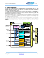
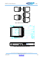
FMC110 User Manual
r1.6
FMC110
User Manual
4DSP LLC
10713 Ranch Road 620 N, Suite 522, Austin, TX 78726, USA
Email: [email protected]
This document is the property of 4DSP LLC and may not be copied nor communicated to a
third party without the written permission of 4DSP LLC.
© 4DSP LLC. 2010
FMC110 User Manual
r1.6
Revision History
Date
Revision
Revision
2010-06-01
Initial release
1.0
2010-07-01
Update in Temperature and voltage parameters
table.
1.1
2010-09-01
Added details about programming the FMC110,
including SPI timing waveforms.
Added FMC signal description in the Appendix.
Added CPLD register definition in the Appendix.
1.2
2010-09-20
Updated photo. Modified block diagram.
1.3
2010-10-03
Text corrections in pin list.
1.4
2010-10-12
Update address. Update block diagram
1.5
2011-01-21
Correction in section 4.1.2.
1.6
4DSP est distribué par TECHWAY - www.techway.fr - [email protected] - +33 (0)1 64 53 37 90
FMC110 User Manual
January 2011
www.4dsp.com
-2-
FMC110 User Manual
r1.6
Table of Contents
1
2
3
4
5
6
7
8
Acronyms and related documents ............................................................................. 5
1.1
Acronyms ................................................................................................................ 5
1.2
Related Documents ................................................................................................. 5
General description ..................................................................................................... 6
Installation ................................................................................................................... 7
3.1
Requirements and handling instructions .................................................................. 7
3.2
LVDS requirements ................................................................................................. 7
Design .......................................................................................................................... 8
4.1
Phycisal specifications ............................................................................................ 8
4.1.1
Board Dimensions ............................................................................................ 8
4.1.2
Front panel coax inputs .................................................................................... 8
4.1.1
Front panel HDMI I/O ....................................................................................... 8
4.1.1
Front I/O (LVTTL/TTL)...................................................................................... 8
4.2
Electrical specifications ........................................................................................... 9
4.2.1
EEPROM ......................................................................................................... 9
4.2.1
JTAG................................................................................................................ 9
4.2.1
FMC HPC......................................................................................................... 9
4.3
Main characteristics................................................................................................11
4.4
Analog input channels ............................................................................................12
4.5
Analog output channels ..........................................................................................12
4.6
External clock input ................................................................................................12
4.7
External trigger/sync input ......................................................................................12
4.8
Clock Tree..............................................................................................................13
4.8.1
Control ............................................................................................................14
4.9
Multi-Gigabit Transceivers ......................................................................................14
4.10
Power supply ......................................................................................................16
4.11
Parallel A/D operation (Fs up to 2GHz) ...............................................................17
4.12
Synchronizing multiple cards ..............................................................................18
Controlling the FMC110..............................................................................................18
5.1
Architecture ............................................................................................................19
5.2
SPI Programming ...................................................................................................20
Environment................................................................................................................21
6.1
Temperature ..........................................................................................................21
6.2
Monitoring ..............................................................................................................21
6.3
Cooling ...................................................................................................................22
6.3.1
Convection cooling ..........................................................................................22
6.3.2
Conduction cooling ..........................................................................................22
Safety...........................................................................................................................22
EMC .............................................................................................................................23
4DSP est distribué par TECHWAY - www.techway.fr - [email protected] - +33 (0)1 64 53 37 90
FMC110 User Manual
January 2011
www.4dsp.com
-3-
FMC110 User Manual
r1.6
9
Warranty ......................................................................................................................23
Appendix A HPC pin-out FMC110 .................................................................................24
Appendix B CPLD Register map ...................................................................................28
4DSP est distribué par TECHWAY - www.techway.fr - [email protected] - +33 (0)1 64 53 37 90
FMC110 User Manual
January 2011
www.4dsp.com
-4-
FMC110 User Manual
r1.6
1 Acronyms and related documents
1.1
Acronyms
ADC
DDR
EPROM
FBGA
FMC
FPGA
JTAG
LED
LVTTL
LSB
LVDS
MGT
MSB
PCB
PLL
PSSR
Analog to Digital Converter
Double Data Rate
Erasable Programmable Read-Only Memory
Fineline Ball Grid Array
FPGA Mezzanine Card
Field Programmable Gate Array
Join Test Action Group
Light Emitting Diode
Low Voltage Transistor Logic level
Least Significant Bit(s)
Low Voltage Differential Signaling
Multi-Gigabit Transceiver
Most Significant Bit(s)
Printed Circuit Board
Phase Locked Loop
Power Supply Rejection Ratio
Table 1: Glossary
1.2
Related Documents
•
•
•
•
•
FPGA Mezzanine Card (FMC) standard ANSI/VITA 57.1-2010
Datasheet ADS5400, TI
Datasheet DAC5681Z, TI
Datasheet AD9517, Analog Devices
Datasheet ADT7411 Rev B, Analog Devices
4DSP est distribué par TECHWAY - www.techway.fr - [email protected] - +33 (0)1 64 53 37 90
FMC110 User Manual
January 2011
www.4dsp.com
-5-
FMC110 User Manual
r1.6
2 General description
The FMC110 is a dual channel A/D and dual channel D/A FMC daughter card. The card
provides two 12-bit A/D channels and two 16-bit D/A channels that enable simultaneous
sampling at a maximum rate of 1 Gsps.
The sample clock can be supplied externally through a coax connection or supplied by an
internal clock source (optionally locked to an external reference). Additionally a trigger input
for customized sampling control is available.
The FMC110 daughter card is mechanically and electrically compliant to FMC standard
(ANSI/VITA 57.1). The card has a high-pin count connector, front panel I/O, and can be used
in a conduction cooled environment.
The FMC110 allows flexible control on clock source, sampling frequency, and calibration
through a SPI communication bus. Furthermore the card is equipped with power supply and
temperature monitoring and offers several power-down modes to switch off unused
functions.
HDMI
MICTOR 38-pins
Multi Gigabit Transceiver
(optional)
MICTOR 38-pins
Multi Gigabit Transceiver
(optional)
FMC High-pin Count 400-pins
LVDS
Figure 1: FMC110 block diagram
4DSP est distribué par TECHWAY - www.techway.fr - [email protected] - +33 (0)1 64 53 37 90
FMC110 User Manual
January 2011
www.4dsp.com
-6-
FMC110 User Manual
r1.6
3 Installation
3.1
Requirements and handling instructions
•
•
•
•
3.2
The FMC110 daughter card must be installed on a carrier card compliant to the FMC
standard.
The FMC carrier card must support the high-pin count connector (HPC 400-pins).
The FMC carrier card must support VADJ/VIO_B voltage of +2.5V (LVDS support).
Do not flex the card and prevent electrostatic discharges by observing ESD
precautions when handling the card.
LVDS requirements
The A/D channels based on TI’s ADS5400 can operate in 1-bus or 2-bus mode. In 1-bus
mode all data is transferred to output port A at a maximum rate of 1Gbps per DDR LVDS
pair. In 2-bus more the data is de-multiplexed over output port A and B at a maximum rate of
500Mpbs per DDR LVDS pair.
Output port B of one A/D channel is not available due to the limited amount of LVDS
connections on the FMC connector. In 2-bus mode the sync feature can be used to re-align
the data coming from the two separate paths on the carrier board.
Each D/A channels have an independent DDR LVDS data bus. The full rate of 1Gsps is
supported, but the digital transfer rate can be lowered by enabling the interpolation (x2 or x4)
in the D/A devices.
4DSP est distribué par TECHWAY - www.techway.fr - [email protected] - +33 (0)1 64 53 37 90
FMC110 User Manual
January 2011
www.4dsp.com
-7-
FMC110 User Manual
r1.6
4 Design
4.1
Phycisal specifications
4.1.1 Board Dimensions
The FMC110 card complies with the FMC standard known as ANSI/VITA 57.1. The card is a
single width conduction cooled mezzanine module (with region 1 and front panel I/O).
4.1.2 Front panel coax inputs
There are 6 coax connectors available from the front panel. From top to bottom; 1st analog
input (A), 1st analog output (B), 2nd analog output (C), 2nd analog input (D), clock input (CL),
trigger input (TR).
Figure 2: Bezel drawing
4.1.1 Front panel HDMI I/O
The 19-pins HDMI connector on the front panel (IO) holds 4 Multi gigabit transceivers (2 Tx
pairs / 2 Rx pairs) and 4x LVTTL I/O (5V tolerant). Contact 4DSP for other configurations.
Pin Number
1
2
3
4
5
6
7
8
9
10
Signal Name
DP_M2C_P<0>
Shield
DP_M2C_N<0>
DP_M2C_P<1>
Shield
DP_M2C_N<1>
DP_C2M_P<2>
Shield
DP_C2M_N<2>
DP_C2M_P<3>
Pin Number
20
19
18
17
16
15
14
13
12
11
Signal Name
GND
N.C.
N.C.
N.C.
FRONT_IO<1>
FRONT_IO<0>
FRONT_IO<3>
FRONT_IO<2>
DP_C2M_N<3>
Shield
Table 2. HDMI connector pin out
4.1.1 Front I/O (LVTTL/TTL)
A voltage translator is used for the (LV)TTL signals available on the front panel. The FMC
side is 2.5V. The front side is either 3.3V for LVTTL or 5.0V for TTL (build option). These
inputs are 5V tolerant when powered with 3.3V. The direction is controlled by the CPLD.
4DSP est distribué par TECHWAY - www.techway.fr - [email protected] - +33 (0)1 64 53 37 90
FMC110 User Manual
January 2011
www.4dsp.com
-8-
FMC110 User Manual
4.2
r1.6
Electrical specifications
The FMC110 uses high speed LVDS outputs and require +2.5V on VADJ power supply
(supplied by the carrier card). The voltage on VIO_B pins (supplied by the FMC) is also
+2.5V. VIO_B is directly connected the VADJ on the FMC110.
4.2.1 EEPROM
The FMC110 card carries a 2Kbit EEPROM (24LC02B) which is accessible from the carrier
card through the I2C bus. The EEPROM is powered by 3P3VAUX. The standby current is
only 0.01µA when SCL and SDA are kept at 3P3VAUX level. These signals may also be left
floating since pull-up resistors are present on the card.
4.2.1 JTAG
The CPLD device is included in the JTAG chain accessible from the FMC connection. The
user should NOT reprogram or erase the CPLD.
4.2.1 FMC HPC
The high-pin count connector has 4 dedicated LVDS clock pairs and can host up to 80 LVDS
(data) pairs. Refer to appendix A for a detailed pin-out.
4DSP est distribué par TECHWAY - www.techway.fr - [email protected] - +33 (0)1 64 53 37 90
FMC110 User Manual
January 2011
www.4dsp.com
-9-
FMC110 User Manual
r1.6
# Pairs
# Clock pairs
LVDS Clock
1
1
LVDS Trigger
1
1
LVDS Sync
1
1
# Data pairs
ADC #1 (port A)
14
LVDS Clock
1
LVDS Data
12
LVDS Ovr / LVDS Sync
ADC #1 (port B)
1
13
LVDS Clock
0
LVDS Data
12
LVDS Ovr / LVDS Sync
1
ADC #2 (port A)
14
LVDS Clock
1
LVDS Data
12
LVDS Ovr / LVDS Sync
1
DAC #1
18
LVDS Clock
1
LVDS Sync
1
LVDS Data
DAC #2
16
17
LVDS Clock
1
LVDS Sync
0
LVDS Data
16
2.5V I/O routed to CPLD
2 (4)
2.5V I/O routed to FRONT
2 (4)
# Total pairs
3
80
1
Table 3. HPC signal usage
1
Signal CLK3_BIDIR_P/N is not connected.
4DSP est distribué par TECHWAY - www.techway.fr - [email protected] - +33 (0)1 64 53 37 90
FMC110 User Manual
January 2011
www.4dsp.com
- 10 -
FMC110 User Manual
4.3
r1.6
Main characteristics
Analog inputs
Number of channels
2
Channel resolution
12-bit
Input voltage range
Max. 1.5Vp-p to 2.0Vp-p (programmable)
Contact 4DSP for a 1Vp-p option to match the A/D input voltage
range with the D/A output voltage range.
Input impedance
Analogue input bandwidth
Performance (Fin = 400 MHz)
Calibration
50Ω AC coupled
2 GHz (TBD)
ENOB = 8.8 bit, SFDR = 64 dBc, SNRFS = 57 dB
Gain ±24%
Offset ±30mV
Phase 0-72ps
Analog outputs
Output voltage range
Max. 1.0Vp-p
Load
50Ω
Performance (Fout = 400 MHz)
TBD
Analogue Bandwidth
Max. 500MHz
External Clock/Reference input
Input level
Input impedance
Input range
250mVp-p to 2.0Vp-p
50Ω AC coupled
10 – 100 MHz (reference clock)
100 – 1000 MHz (sample clock)
External Trigger/Sync input
Format
150 mVp-p typical (LVTTL level supported)
Input impedance
10kΩ DC coupled (50Ω AC coupled option available)
Frequency range
Up to 500 MHz
ADC Output
Output data width
Data Format
Sampling Frequency Range
1-bus mode, 1x 12-pairs DDR 1Gbps
2-bus mode, 2x 12-pairs DDR 500Mbps
Two’s Complement / Offset binary
100 – 1000 MHz
Internal Clock/Reference
Format
Frequency Range
LVPECL
100 MHz (reference clock)
100, 125, 200, 250, 500, or 1000 MHz (sample clock)
(contact 4DSP for customized frequencies)
Table 4 : FMC110 daughter card main characteristics
4DSP est distribué par TECHWAY - www.techway.fr - [email protected] - +33 (0)1 64 53 37 90
FMC110 User Manual
January 2011
www.4dsp.com
- 11 -
FMC110 User Manual
4.4
r1.6
Analog input channels
The FMC110 has two single ended analog inputs AC coupled to the A/D devices. A
wideband RF transformer (TC1-1-13M, 4.5-3000MHz) is used. The maximum input voltage
range is programmable in the A/D device from 1.5VP-P to 2.0VP-P.
4.5
Analog output channels
The FMC110 has two single ended analog outputs AC coupled from the D/A device. An RF
transformer (TC4-1W, 3-800MHz) is used. The analog outputs are designed to drive a 50Ω
load. The maximum output voltage range is 1.0VP-P.
4.6
External clock input
The external clock input can be configured in two ways (see also Figure 5):
1. Sample clock input, connecting to the clock input of the AD9517.
2. Reference clock input, connecting to the reference input of the AD9517.
4.7
External trigger/sync input
The external trigger input can be configured in different ways (build options). The trigger
input can be 50Ω terminated accepting most common high speed signalling standards like
single ended LVPECL. As a build option the 50Ω termination can be removed to support
LVTTL/LVCMOS and similar input standards. Differential input is also possible using the
coax shield as inverted signal. By default the input is DC coupled with a 10k termination to
ground.
Optionally the trigger input can be used as sync input, synchronizing local A/D and D/A
converters, or synchronizing multiple FMC110 cards.
Figure 3: A/D Synchronization topology
In order to correctly align the digital output samples (when A/D in 2-bus mode or two A/D
parallel) a reset signal needs to be generated. This can be a single pulse, a repetitive pulse,
or a low-to-high step. As a result of the reset input a pulse is generated on the sync output.
The carrier hardware must use these sync pulses to correctly align the digital output
samples.
4DSP est distribué par TECHWAY - www.techway.fr - [email protected] - +33 (0)1 64 53 37 90
FMC110 User Manual
January 2011
www.4dsp.com
- 12 -
FMC110 User Manual
r1.6
Figure 4: D/A Synchronization topology
Synchronization of multiple D/A devices in parallel is done through the SYNC input. The
SYNC signal is driven by the FPGA (can be derived from the trigger input). Since the SYNC
input has an internal 100R termination resistor a 1: 2 fan-out buffer is used to connect a
single LVDS signal to both D/A converters.
4.8
Clock Tree
The FMC110 offers a clock architecture that combines flexibility and high performance.
Components have been chosen in order to minimize jitter and phase noise to reduce
degradation of the data conversion performance. The user may choose to use an external
sampling clock or an internal sampling clock.
The clock tree has a PLL and clock distribution section. The PLL ensures locking of the
internal clock to an external supplied reference. There is an onboard reference which is used
in case there is no external reference present.
A VC(X)O is used as internal clock source and can connect to the distribution section instead
of the external clock input. The distribution section drives the A/D and D/A devices with the
LVPECL outputs. One LVDS clock output is connected to the FMC connector as a reference
for the digital data transferred to the D/A devices. One LVDS clock output connects to the
synchronisation circuitry.
4DSP est distribué par TECHWAY - www.techway.fr - [email protected] - +33 (0)1 64 53 37 90
FMC110 User Manual
January 2011
www.4dsp.com
- 13 -
FMC110 User Manual
r1.6
Figure 5: Clock tree
4.8.1 Control
The AD9517 supports polarity change on the LVPECL outputs. This enables parallel
operation of the A/D converters, see section 4.11.
The clock tree contains two RF switches (ADG918) and requires the following control signals
(driven from the CPLD):
• CLKSRC_SEL0 connects the external clock input to the reference input of the
AD9517 or the 2nd RF switch.
• CLKSRC_SEL1 connect either the onboard VCXO or the external clock to the clock
input of the AD9510. This signal also controls the VCXO power supply2.
• CLKSRC_SEL2 enables/disables the onboard reference oscillator.
4.9
Multi-Gigabit Transceivers
The FMC connector hosts 10 MGT pairs (10 Tx and 10 Rx pairs). These are connected to
two 38-pins MICTOR headers. The arrangement is such that different interconnect
topologies are supported;
2
The VCXO should be powered down to avoid interference with the external clock when external
clock is used.
4DSP est distribué par TECHWAY - www.techway.fr - [email protected] - +33 (0)1 64 53 37 90
FMC110 User Manual
January 2011
www.4dsp.com
- 14 -
FMC110 User Manual
5Rx/5Tx
5Rx/5Tx
5Rx/5Tx
r1.6
5Rx/5Tx
5Rx/5Tx
5Rx/5Tx
5Rx/5Tx
5Rx/5Tx
5Rx/5Tx
5Rx/5Tx
Figure 6: MGT interconnect topologies
Figure 7: 4DSP CPCI board stack (slot-to-slot)
4DSP est distribué par TECHWAY - www.techway.fr - [email protected] - +33 (0)1 64 53 37 90
FMC110 User Manual
January 2011
www.4dsp.com
- 15 -
FMC110 User Manual
r1.6
Pin
Signal
Midplate
Signal
Pin
Pin
Signal
Midplate
Signal
Pin
1
3
5
7
9
11
13
15
17
19
21
23
25
27
29
31
33
35
37
GND
TX0_P*
TX0_N*
GND
TX1_P*
TX1_N*
GND
TX2_P*
TX2_N*
GND
TX3_P*
TX3_N*
GND
TX4_P
TX4_N
GND
IO0
IO1
GND
GND
GND
GND
GND
GND
GND
GND
GND
GND
GND
GND
GND
GND
GND
GND
GND
GND
GND
GND
GND
RX0_P*
RX0_N*
GND
RX1_P*
RX1_N*
GND
RX2_P*
RX2_N*
GND
RX3_P*
RX3_N*
GND
RX4_P
RX4_N
GND
2
4
6
8
10
12
14
16
18
20
22
24
26
28
30
32
34
36
38
1
3
5
7
9
11
13
15
17
19
21
23
25
27
29
31
33
35
37
GND
RX9_P
RX9_N
GND
RX8_P
RX8_N
GND
RX7_P
RX7_N
GND
RX6_P
RX6_N
GND
RX5_P
RX5_N
GND
IO2
IO3
GND
GND
GND
GND
GND
GND
GND
GND
GND
GND
GND
GND
GND
GND
GND
GND
GND
GND
GND
GND
GND
TX9_P
TX9_N
GND
TX8_P
TX8_N
GND
TX7_P
TX7_N
GND
TX6_P
TX6_N
GND
TX5_P
TX5_N
GND
2
4
6
8
10
12
14
16
18
20
22
24
26
28
30
32
34
36
38
GND
Table 5: MGT connector pin out
GND
3
A low phase noise 125MHz XTAL is used as reference clock. A 1:2 LVDS fan-out buffer is
used to fed to reference clock to both connections on the FMC connector.
The pairs marked with * connects to either the MICTOR header or the HDMI connector. The
assembly is determined with 0Ω resistors. A maximum of four pairs can connect to the HDMI
connector. Contact 4DSP for custom configurations.
4.10 Power supply
Power is supplied to the FMC110 card through the FMC connector. The pin current rating is
2.7A, but the overall maximum as specified by the FMC standard is limited according to
Table 6.
3
Signals IO[0:3] connects to the CPLD and has no defined function yet.
4DSP est distribué par TECHWAY - www.techway.fr - [email protected] - +33 (0)1 64 53 37 90
FMC110 User Manual
January 2011
www.4dsp.com
- 16 -
FMC110 User Manual
r1.6
Voltage
+3.3V
+12V
VADJ (+2.5V)
VIO_B (+2.5V)
# pins
4
2
4
2
Max Amps
3A
1A
4A
1.15 A
Max Watt
10 W
12 W
10 W
2.3 W
Table 6: FMC standard power specification
The power provided by the carrier card can be very noisy. Special care is taken with the
power supply generation on the FMC110 card to minimize the effect of power supply noise
on clock generation and data conversion.
Clean analog supply is derived from +12V in two steps for maximum efficiency. The first step
uses a high efficient switched regulator. From this power rail the analog supply is derived
with low dropout, low noise, high PSRR, linear regulators. At several stages in the power
supply there is additional noise filtering.
The regulators have sufficient copper area to dissipate the heat in combination with proper
airflow (see section 6.3 Cooling)
Power plane
VADJ
3P3V
12P0V
3P3VAUX (Operating)
3P3VAUX (Standby)
Typical
674 mA
105 mA
913 mA
0.1 mA
0.01 µA
Maximum
3 mA
1 µA
Table 7: Typical/Maximum current drawn from FMC carrier card
The total power consumption: 12W
4.11 Parallel A/D operation (Fs up to 2GHz)
Both A/D converters can operate in parallel, capturing the same signal, but clocked with 180
degree clock phase difference. The out of phase clocks are generated locally. The analog
signal needs to be split externally.
Fs 50%
Clock generation
Fs/4 25%
Analog Input
CLOCK
optional
TRIGGER/SYNC
AIN 1
ADC #1
AIN 2
ADC #2
FMC110
SIGNAL
SPLITTER
Figure 8: Parallel A/D operation
4DSP est distribué par TECHWAY - www.techway.fr - [email protected] - +33 (0)1 64 53 37 90
FMC110 User Manual
January 2011
www.4dsp.com
- 17 -
FMC110 User Manual
r1.6
Gain, phase, and offset errors may be compensated by the calibration features of the
ADS5400 when not exceeding the programmability range (refer to Table 4).
The INL (integral non-linearity) of the converters needs to be taken into account. INL
represents the number of LSBs the output of a converter is from the expected output for a
given input voltage. For example, if a converter would ideally put out a code of N for an input
voltage M but actually puts out a code N+2, then the INL at that point is two. The ADS5400
has an INL of ±2 LSB (±4 LSB maximum). When interleaving converters, the output codes
could differ by as much as 8 LSB for the same input voltage and may drastically reduce the
number of effective bits.
A single device has a typical performance of 57dBFS (Fin= 1.2GHz). The INL specification of
the ADS5400 makes high performance interleaving difficult. A very rough estimation is that
the SNR can decrease below 50dBFS, even if phase, offset, and gain calibration has been
performed. INL problems can partly be corrected in the digital domain, but may require
lengthy calibration.
4.12 Synchronizing multiple cards
Multiple cards can be synchronized together. The cards need to be supplied with
synchronized clock signals. In addition an external synchronization signal is required to be
able to align the samples in the digital domain. Refer to section 4.7 for details about
synchronisation.
Fs 50%
CLOCK
Fs/4 25%
TRIGGER/SYNC
Clock generation
FMC110
CLOCK
TRIGGER/SYNC
FMC110
CLOCK
TRIGGER/SYNC
FMC110
Figure 9: Synchronizing multiple cards
5 Controlling the FMC110
4DSP est distribué par TECHWAY - www.techway.fr - [email protected] - +33 (0)1 64 53 37 90
FMC110 User Manual
January 2011
www.4dsp.com
- 18 -
FMC110 User Manual
5.1
r1.6
Architecture
The FMC needs to be controlled from the carrier hardware through a single SPI
communication bus. The SPI communication bus is connected to a CPLD which has the
following tasks:
• Distribute SPI access from the carrier hardware along the local devices:
- 2x ADS5400 (A/D converters)
- 2x DAC5681Z (D/A converters)
- 1x AD9517 (Clock Tree)
• Select clock source based on a SPI command from the carrier hardware
(CLKSRC_SEL).
• Select sync source based on a SPI command from the carrier hardware
(SYNCSRC_SEL).
• Generate SPI reset for AD9517 (CLK_N_RESET) and both DAC5681Z
(DAC_N_RESET)
• Control the direction of the front I/O transceivers (FRONT_IO_DIR).
• Control the FAN header power (FAN_N_EN).
• Collect local status signals and store them in a register which can be accessed from
the carrier hardware.
• Drive a LED according to the level of the status signals.
Figure 10: CPLD architecture
Notes:
• SDO on the AD9517, ADS5400, and DAC5681Z devices is not connected. SDIO is
used bidirectional (3-wire SPI)
• N_SYNC and N_PD on the AD9517 are not connected.
• ENA1BUS and ENPWD on the ADS5400 are not connected.
4DSP est distribué par TECHWAY - www.techway.fr - [email protected] - +33 (0)1 64 53 37 90
FMC110 User Manual
January 2011
www.4dsp.com
- 19 -
FMC110 User Manual
•
5.2
r1.6
N_RESET on the both DAC5681Z devices is shared.
SPI Programming
The SPI programmable devices on the FMC110 can be accessed as described in their
datasheet, but each SPI communication cycle needs to be preceded with a pre-selection
byte. The pre-selection byte is used by the CPLD to forward the SPI command to the right
destination. The pre-selection bytes are defined as follows:
- CPLD
0x00
- ADS5400
#1
0x80
- ADS5400
#2
0x81
- DAC5681Z #1
0x82
- DAC5681Z #2
0x83
- AD9517
0x84
The CLPD has three internal registers which are described in Appendix B CPLD Register
map. The registers of the other devices are transparently mapped.
Figure 11: Write instruction to CPLD registers A1:A0
Figure 12: Read instruction to CPLD registers A1:A0
Figure 13: Write instruction to ADS5400 / DAC5681Z registers A4:A0
4DSP est distribué par TECHWAY - www.techway.fr - [email protected] - +33 (0)1 64 53 37 90
FMC110 User Manual
January 2011
www.4dsp.com
- 20 -
FMC110 User Manual
r1.6
Figure 14. Read instruction to ADS5400 / DAC5681Z registers A4:A0
Figure 15: Write instruction to AD9517 registers A12:A0
Figure 16: Read instruction to AD9517 registers A12:A0
6 Environment
6.1
Temperature
Operating temperature:
• -40°C to +85°C (Industrial)
Storage temperature:
• -40°C to +120°C
6.2
Monitoring
The onboard monitoring may be used to monitor the voltage on the different power rails as
well as the temperature of the A/D devices.
It is recommended that the carrier card and/or host software uses the power-down features
in the case the temperature is too high. Normal operations can resume once the temperature
is within the operating conditions boundaries.
4DSP est distribué par TECHWAY - www.techway.fr - [email protected] - +33 (0)1 64 53 37 90
FMC110 User Manual
January 2011
www.4dsp.com
- 21 -
FMC110 User Manual
Parameter:
r1.6
Device 1
address 1001 000
Formula
On-chip temperature
On-chip AIN0 (VDD)
+3.3V
External AIN1
+3.3V Analog CLK
AIN1 * 2
External AIN2
+1.8V Digital
AIN2
External AIN3
VADJ
AIN3
External AIN4
+2.5V Analog CLK
AIN4
External AIN5
+3.3V Digital
AIN5 * 2
External AIN6
+3.3V Analog ADC
AIN6 * 2
External AIN7
+3.3V VCP
AIN7 * 2
External AIN8
+12V
AIN8 * 7.04
Table 8: Temperature and voltage parameters
6.3
Cooling
Two different types of cooling will be available for the FMC110.
6.3.1 Convection cooling
The air flow provided by the chassis fans the FMC110 is enclosed in will dissipate the heat
generated by the on board components. A minimum airflow of 300 LFM is recommended.
Optionally low profile FANs can be glued on top of the A/D devices. The card has a FAN
power connection that can be switch on and off under carrier card control (individually driven
from the CPLD).
For stand alone operations (such as on a Xilinx development kit), it is highly recommended to
blow air across the FMC and ensure that the temperature of the devices is within the allowed
range. 4DSP’s warranty does not cover boards on which the maximum allowed temperature
has been exceeded.
6.3.2 Conduction cooling
In demanding environments, the ambient temperature inside a chassis could be close to the
operating temperature defined in this document. It is very likely that in these conditions the
junction temperature of power consuming devices will exceed the operating conditions
recommended by the devices manufacturers (mostly +85°C).
The FMC110 is designed for maximum heat transfer to conduction cooled ribs. A customized
cooling frame that connects directly to the surface of the A/D devices is allowed (contact
4DSP for detailed mechanical information). This conduction cooling mechanism should be
applied in combination with proper chassis air flow.
7 Safety
This module presents no hazard to the user.
4DSP est distribué par TECHWAY - www.techway.fr - [email protected] - +33 (0)1 64 53 37 90
FMC110 User Manual
January 2011
www.4dsp.com
- 22 -
FMC110 User Manual
r1.6
8 EMC
This module is designed to operate from within an enclosed host system, which is build to
provide EMC shielding. Operation within the EU EMC guidelines is not guaranteed unless it
is installed within an adequate host system. This module is protected from damage by fast
voltage transients originating from outside the host system which may be introduced through
the system.
9 Warranty
Hardware
Software/Firmware
Basic Warranty
(included)
1 Year from Date of Shipment
90 Days from Date of Shipment
Extended Warranty
(optional)
2 Years from Date of Shipment
1 Year from Date of Shipment
4DSP est distribué par TECHWAY - www.techway.fr - [email protected] - +33 (0)1 64 53 37 90
FMC110 User Manual
January 2011
www.4dsp.com
- 23 -
FMC110 User Manual
r1.6
Appendix A HPC pin-out FMC110
AV57.1
FMC110 Signal
AV57.1
HPC Pin
FMC110 Signal
AV57.1
HPC Pin
CLK0_M2C_N
HPC Pin
H5
CLK_TO_FPGA_N
HA00_N_CC
F5
ADC1_OVRA_N
HB10_N
K32
FMC110 Signal
DAC1_DATA_P<4>
CLK0_M2C_P
H4
CLK_TO_FPGA_P
HA00_P_CC
F4
ADC1_OVRA_P
HB10_P
K31
DAC1_DATA_N<4>
CLK1_M2C_N
G3
TRIGGER_TO_FPGA_N
HA01_N_CC
E3
ADC0_CLKA_N
HB11_N
J31
DAC1_DATA_P<5>
CLK1_M2C_P
G2
TRIGGER_TO_FPGA_P
HA01_P_CC
E2
ADC0_CLKA_P
HB11_P
J30
DAC1_DATA_N<5>
CLK2_BIDIR_N
K5
SYNC_FROM_FPGA_N
HA02_N
K8
ADC0_DA_N<8>
HB12_N
F32
DAC1_DATA_P<3>
CLK2_BIDIR_P
K4
SYNC_FROM_FPGA_P
HA02_P
K7
ADC0_DA_P<8>
HB12_P
F31
DAC1_DATA_N<3>
CLK3_BIDIR_N
J3
N.C.
HA03_N
J7
ADC0_DA_N<10>
HB13_N
E31
DAC1_DATA_P<6>
CLK3_BIDIR_P
J2
N.C.
HA03_P
J6
ADC0_DA_P<10>
HB13_P
E30
DAC1_DATA_N<6>
LA00_N_CC
G7
ADC0_DB_N<9>
HA04_N
F8
ADC0_DA_N<9>
HB14_N
K35
DAC1_DATA_P<1>
LA00_P_CC
G6
ADC0_DB_P<9>
HA04_P
F7
ADC0_DA_P<9>
HB14_P
K34
DAC1_DATA_N<1>
LA01_N_CC
D9
ADC0_DA_N<7>
HA05_N
E7
ADC0_DA_N<11>
HB15_N
J34
DAC1_DATA_P<2>
LA01_P_CC
D8
ADC0_DA_P<7>
HA05_P
E6
ADC0_DA_P<11>
HB15_P
J33
DAC1_DATA_N<2>
LA02_N
H8
ADC0_DB_N<7>
HA06_N
K11
ADC0_DA_N<5>
HB16_N
F35
DAC1_DATA_P<0>
LA02_P
H7
ADC0_DB_P<7>
HA06_P
K10
ADC0_DA_P<5>
HB16_P
F34
DAC1_DATA_N<0>
LA03_N
G10
ADC0_DB_N<8>
HA07_N
J10
ADC0_DA_N<0>
HB17_N_CC
K38
ADC0_DB_N<1>
LA03_P
G9
ADC0_DB_P<8>
HA07_P
J9
ADC0_DA_P<0>
HB17_P_CC
K37
ADC0_DB_P<1>
LA04_N
H11
ADC0_DB_N<6>
HA08_N
F11
ADC0_DB_N<9>
HB18_N
J37
ADC0_DB_N<0>
LA04_P
H10
ADC0_DB_P<6>
HA08_P
F10
ADC0_DA_P<1>
HB18_P
J36
ADC0_DB_P<0>
LA05_N
D12
ADC0_DA_N<3>
HA09_N
E10
ADC0_DA_N<6>
HB19_N
E34
ADC0_DB_N<5>
LA05_P
D11
ADC0_DA_P<3>
HA09_P
E9
ADC0_DA_P<6>
HB19_P
E33
ADC0_DB_P<5>
LA06_N
C11
ADC0_OVRA_N
HA10_N
K14
ADC0_DA_N<4>
HB20_N
F38
FRONT_IO<1>
LA06_P
C10
ADC0_OVRA_P
HA10_P
K13
ADC0_DA_P<4>
HB20_P
F37
FRONT_IO<0>
LA07_N
H14
ADC0_DA_N<2>
HA11_N
J13
ADC1_DA_N<10>
HB21_N
E37
FRONT_IO<3>
LA07_P
H13
ADC0_DA_P<2>
HA11_P
J12
ADC1_DA_P<10>
HB21_P
E36
FRONT_IO<2>
LA08_N
G13
DAC_SYNC_N
HA12_N
F14
ADC1_DA_N<8>
GBTCLK0_M2C_N
D5
GBTCLK0_N
LA08_P
G12
DAC_SYNC_P
HA12_P
F13
ADC1_DA_P<8>
GBTCLK0_M2C_P
D4
GBTCLK0_P
LA09_N
D15
FMC_TO_CPLD<1>
HA13_N
E13
ADC1_DA_N<11>
GBTCLK1_M2C_N
B21
GBTCLK1_N
LA09_P
D14
FMC_TO_CPLD<0>
HA13_P
E12
ADC1_DA_P<11>
GBTCLK1_M2C_P
B20
GBTCLK1_P
LA10_N
C15
FMC_TO_CPLD<3>
HA14_N
J16
ADC1_DA_N<9>
DP0_C2M_N
C3
DP_C2M_N<0>
LA10_P
C14
FMC_TO_CPLD<2>
HA14_P
J15
ADC1_DA_P<9>
DP0_C2M_P
C2
DP_C2M_P<0>
LA11_N
H17
ADC0_DB_N<10>
HA15_N
F17
ADC1_DA_N<2>
DP0_M2C_N
C7
DP_M2C_N<0>
LA11_P
H16
ADC0_DB_P<10>
HA15_P
F16
ADC1_DA_P<2>
DP0_M2C_P
C6
DP_M2C_P<0>
LA12_N
G16
DAC0_DATA_P<15>
HA16_N
E16
ADC1_DA_N<7>
DP1_C2M_N
A23
DP_C2M_N<1>
LA12_P
G15
DAC0_DATA_N<15>
HA16_P
E15
ADC1_DA_P<7>
DP1_C2M_P
A22
DP_C2M_P<1>
LA13_N
D18
DAC0_DATA_P<14>
HA17_N_CC
K17
ADC1_CLKA_N
DP1_M2C_N
A3
DP_M2C_N<1>
LA13_P
D17
DAC0_DATA_N<14>
HA17_P_CC
K16
ADC1_CLKA_P
DP1_M2C_P
A2
DP_M2C_P<1>
LA14_N
C19
DAC0_DATA_P<13>
HA18_N
J19
ADC1_DA_N<4>
DP2_C2M_N
A27
DP_C2M_N<2>
LA14_P
C18
DAC0_DATA_N<13>
HA18_P
J18
ADC1_DA_P<4>
DP2_C2M_P
A26
DP_C2M_P<2>
LA15_N
H20
DAC0_DATA_P<12>
HA19_N
F20
ADC1_DA_N<3>
DP2_M2C_N
A7
DP_M2C_N<2>
LA15_P
H19
DAC0_DATA_N<12>
HA19_P
F19
ADC1_DA_P<3>
DP2_M2C_P
A6
DP_M2C_P<2>
LA16_N
G19
ADC0_DB_N<11>
HA20_N
E19
ADC1_DA_N<0>
DP3_C2M_N
A31
DP_C2M_N<3>
LA16_P
G18
ADC0_DB_P<11>
HA20_P
E18
ADC1_DA_P<0>
DP3_C2M_P
A30
DP_C2M_P<3>
LA17_N_CC
D21
ADC0_DB_N<3>
HA21_N
K20
ADC1_DA_N<6>
DP3_M2C_N
A11
DP_M2C_N<3>
LA17_P_CC
D20
ADC0_DB_P<3>
HA21_P
K19
ADC1_DA_P<6>
DP3_M2C_P
A10
DP_M2C_P<3>
4DSP est distribué par TECHWAY - www.techway.fr - [email protected] - +33 (0)1 64 53 37 90
FMC110 User Manual
r1.6
LA18_N_CC
C23
ADC0_DB_N<4>
HA22_N
J22
ADC1_DA_N<5>
DP4_C2M_N
A35
DP_C2M_N<4>
LA18_P_CC
C22
ADC0_DB_P<4>
HA22_P
J21
ADC1_DA_P<5>
DP4_C2M_P
A34
DP_C2M_P<4>
LA19_N
H23
DAC0_DATA_P<10>
HA23_N
K23
ADC1_DA_N<1>
DP4_M2C_N
A15
DP_M2C_N<4>
LA19_P
H22
DAC0_DATA_N<10>
HA23_P
K22
ADC1_DA_P<1>
DP4_M2C_P
A14
DP_M2C_P<4>
LA20_N
G22
DAC0_DATA_P<11>
HB00_N_CC
K26
DAC1_DATA_P<11>
DP5_C2M_N
A39
DP_C2M_N<5>
LA20_P
G21
DAC0_DATA_N<11>
HB00_P_CC
K25
DAC1_DATA_N<11>
DP5_C2M_P
A38
DP_C2M_P<5>
LA21_N
H26
ADC0_DB_N<2>
HB01_N
J25
DAC1_DATA_P<12>
DP5_M2C_N
A19
DP_M2C_N<5>
LA21_P
H25
ADC0_DB_P<2>
HB01_P
J24
DAC1_DATA_N<12>
DP5_M2C_P
A18
DP_M2C_P<5>
LA22_N
G25
DAC0_DATA_P<8>
HB02_N
F23
DAC1_DATA_P<14>
DP6_C2M_N
B37
DP_C2M_N<6>
LA22_P
G24
DAC0_DATA_N<8>
HB02_P
F22
DAC1_DATA_N<14>
DP6_C2M_P
B36
DP_C2M_P<6>
LA23_N
D24
DAC0_DATA_P<9>
HB03_N
E22
DAC1_DATA_P<15>
DP6_M2C_N
B17
DP_M2C_N<6>
LA23_P
D23
DAC0_DATA_N<9>
HB03_P
E21
DAC1_DATA_N<15>
DP6_M2C_P
B16
DP_M2C_P<6>
LA24_N
H29
DAC0_DATA_P<6>
HB04_N
F26
DAC1_DATA_P<10>
DP7_C2M_N
B33
DP_C2M_N<7>
LA24_P
H28
DAC0_DATA_N<6>
HB04_P
F25
DAC1_DATA_N<10>
DP7_C2M_P
B32
DP_C2M_P<7>
LA25_N
G28
DAC0_DATA_P<7>
HB05_N
E25
DAC1_DATA_P<13>
DP7_M2C_N
B13
DP_M2C_N<7>
LA25_P
G27
DAC0_DATA_N<7>
HB05_P
E24
DAC1_DATA_N<13>
DP7_M2C_P
B12
DP_M2C_P<7>
LA26_N
D27
DAC0_DCLK_N
HB06_N_CC
K29
DAC1_DCLK_N
DP8_C2M_N
B29
DP_C2M_N<8>
LA26_P
D26
DAC0_DCLK_P
HB06_P_CC
K28
DAC1_DCLK_P
DP8_C2M_P
B28
DP_C2M_P<8>
LA27_N
C27
DAC0_DATA_P<5>
HB07_N
J28
DAC1_DATA_P<8>
DP8_M2C_N
B9
DP_M2C_N<8>
LA27_P
C26
DAC0_DATA_N<5>
HB07_P
J27
DAC1_DATA_N<8>
DP8_M2C_P
B8
DP_M2C_P<8>
LA28_N
H32
DAC0_DATA_P<3>
HB08_N
F29
DAC1_DATA_P<7>
DP9_C2M_N
B25
DP_C2M_N<9>
LA28_P
H31
DAC0_DATA_N<3>
HB08_P
F28
DAC1_DATA_N<7>
DP9_C2M_P
B24
DP_C2M_P<9>
LA29_N
G31
DAC0_DATA_P<4>
HB09_N
E28
DAC1_DATA_P<9>
DP9_M2C_N
B5
DP_M2C_N<9>
LA29_P
G30
DAC0_DATA_N<4>
HB09_P
E27
DAC1_DATA_N<9>
DP9_M2C_P
B4
DP_M2C_P<9>
LA30_N
H35
DAC0_DATA_P<1>
LA30_P
H34
DAC0_DATA_N<1>
LA31_N
G34
DAC0_DATA_P<2>
LA31_P
G33
DAC0_DATA_N<2>
LA32_N
H38
DAC0_DATA_P<0>
LA32_P
H37
DAC0_DATA_N<0>
LA33_N
G37
ADC0_OVRB_N
LA33_P
G36
ADC0_OVRB_P
4DSP est distribué par TECHWAY - www.techway.fr - [email protected] - +33 (0)1 64 53 37 90
FMC110 User Manual
January 2011
www.4dsp.com
- 25 -
FMC110 User Manual
r1.6
Table 9: HPC signal description (FMC110)
Signal
Group
Direction
I/O Standard
Description
ADC0_CLKA_N
ADC0_CLKA_P
A/D 0
Output
LVDS
Digital data clock from 1 ADC. This ADC can operate in
mux mode, using data port A and data port B
ADC0_DA_N<11..0>
ADC0_DA_P<11..0>
A/D 0
Output
LVDS
Data port A of 1 ADC. Data is valid on both edges of
ADC0_CLKA_P/N (DDR)
ADC0_OVRA_N
ADC0_OVRA_P
A/D 0
Output
LVDS
Over-range bit synchronous to the samples present on port
st
A of 1 ADC. Can be used as sync signal.
ADC0_DB_N<11..0>
ADC0_DB_P<11..0>
A/D 0
Output
LVDS
Data port B of 1 ADC. Data is valid on both edges of
ADC0_CLKA_P/N (DDR)
ADC0_OVRB_N
ADC0_OVRB_P
A/D 0
Output
LVDS
Over-range bit synchronous to the samples present on port
st
B of 1 ADC. Can be used as sync signal.
ADC1_CLKA_N
ADC1_CLKA_P
A/D 1
Output
LVDS
Digital data clock from 2 ADC. This ADC cannot operate in
mux mode, using data port A only
ADC1_DA_N<11..0>
ADC1_DA_P<11..0>
A/D 1
Output
LVDS
Data port A of 2 ADC. Data is valid on both edges of
ADC1_CLKA_P/N (DDR)
ADC1_OVRA_N
ADC1_OVRA_P
A/D 1
Output
LVDS
Over-range bit synchronous to the samples present on port
nd
A of 2 ADC. Can be used as sync signal.
SYNC_FROM_FPGA_N
SYNC_FROM_FPGA_P
A/D 0, A/D 1
Input
LVDS
Signal used to apply a sync pulse to both ADCs in order to
align the digital outputs on sample basis.
CLK_TO_FPGA_N
CLK_TO_FPGA_P
D/A 0, D/A 1
Output
LVDS
Clock to be used as reference clock for generating DAC
clock and data signals. Typically ½ times the sample clock
frequency.
DAC0_DCLK_N
DAC0_DCLK_P
D/A 0
Output
LVDS
Digital data clock to 1 DAC.
DAC0_DATA_N<15..0>
DAC0_DATA_P<15..0>
D/A 0
Output
LVDS
Data bus to 1 DAC. Data should be valid on both edges of
DAC0_DCLK_P/N (DDR)
st
st
st
nd
nd
st
st
4DSP est distribué par TECHWAY - www.techway.fr - [email protected] - +33 (0)1 64 53 37 90
FMC110 User Manual
r1.6
nd
DAC1_DCLK_N
DAC1_DCLK_P
D/A 1
Output
LVDS
Digital data clock to 2 DAC.
DAC1_DATA_N<15..0>
DAC1_DATA_P<15..0>
D/A 1
Output
LVDS
Data bus to 2 DAC. Data should be valid on both edges of
DAC0_DCLK_P/N (DDR)
D/A 0, D/A 1
Input
LVDS
Signal used as transmit enable for both DACs.
TRIGGER_TO_FPGA_N
TRIGGER_TO_FPGA_P
TRIGGER
Output
LVDS
Representation of the signal connected to the external
trigger input.
FMC_TO_CPLD<0>
CONTROL
Input
CMOS VIO
SPI clock connected to the CPLD
FMC_TO_CPLD<1>
CONTROL
Input
CMOS VIO
SPI chip select connected to the CPLD
FMC_TO_CPLD<2>
CONTROL
Bidir
CMOS VIO
SPI data in/out connected to the CPLD
FMC_TO_CPLD<3>
CONTROL
Output
CMOS VIO
Interrupt connected the CPLD (reserved for future use)
I/O
Bidir
CMOS VIO
Connected to the transceivers on the HDMI connector
(Table 2). The direction of the transceivers is controlled
through a CPLD register.
DAC_SYNC_N
DAC_SYNC_P
FRONT_IO<3..0>
nd
4DSP est distribué par TECHWAY - www.techway.fr - [email protected] - +33 (0)1 64 53 37 90
FMC110 User Manual
January 2011
www.4dsp.com
- 27 -
FMC110 User Manual
r1.6
Appendix B CPLD Register map
Bit nr.
Bit 7
Bit 6
Bit 5
Name
‘0’
DACR
CLKR
Bit 4
Bit 3
Bit 2
SYNCSRC
Bit 1
Bit 0
CLKSRC
Table 10: Register CPLD_REG0 definition
Field
Description
CLKSRC
Selection of clock source
‘000’
External clock
‘011’
Internal clock, External Reference
‘110’
Internal clock, Internal Reference
others
Do not use
SYNCSRC
Selection of synchronisation source
‘00‘
External Trigger
‘01‘
Carrier (trough SYNC_FROM_FPGA_P/N)
‘10‘
Clock Tree
‘11‘
No Sync
CLKR
Clock tree SPI reset
‘0‘
Normal operation
‘1‘
Reset, resetting the clock tree is normally not required. This bit is not
self clearing.
DACR
D/A device SPI reset
‘0‘
Normal operation
‘1‘
Reset, resetting the D/A device is normally not required. This bit is
not self clearing.
Table 11 Register CPLD_REG0 description
Bit nr.
Bit 7
Bit 6
Bit 5
Bit 4
Bit 3
Bit 2
Bit 1
Bit 0
Name
FAN3
FAN2
FAN1
FAN0
DIR3
DIR2
DIR1
DIR0
Table 12: Register CPLD_REG1 definition
4DSP est distribué par TECHWAY - www.techway.fr - [email protected] - +33 (0)1 64 53 37 90
FMC110 User Manual
r1.6
Field
Description
DIRx
Direction of Front IO transceiver (x = 0 to 3)
‘0’
Signal x is input (FMC110 is receiver)
‘1’
Signal x is output (FMC110 is transmitter)
FANx
Power control for FAN header (x = 0 to 3)
‘0‘
Apply power to FAN header x
‘1‘
Cut power to FAN header x
Table 13 Register CPLD_REG1 description
Bit nr.
Bit 7
Name
Bit 6
Bit 5
Reserved
Bit 4
Bit 3
Bit 2
Bit 1
Bit 0
IRQ
VM
STATUS
LD
REFMON
Table 14: Register CPLD_REG2 definition (read)
Field
Description
REFMON
LD
Reflect the status of the REFMON output of the AD9517
Reflect the status of the LD output of the AD9517
STATUS
VM
Reflect the status of the STATUS output of the AD9517
Reflect the status of the INT# output of the ADT7411 (inverted)
‘0‘
INT# is not asserted
‘1‘
INT# is asserted, access to the ADT7411 trough the I2C bus is required to
determine the source of the interrupt
IRQ
Logic function: NOT (REFMON AND LD AND STATUS AND INT#)
‘0‘
All status signals indicate OK
‘1‘
One or more status signals indicate ERROR
Table 15 Register CPLD_REG2 description (read)
Bit nr.
Bit 7
Name
Bit 6
Bit 5
Bit 4
Bit 3
Bit 2
Bit 1
Bit 0
LED_SEL
Reserved
Table 16: Register CPLD_REG2 definition (write)
4DSP est distribué par TECHWAY - www.techway.fr - [email protected] - +33 (0)1 64 53 37 90
FMC110 User Manual
January 2011
www.4dsp.com
- 29 -
FMC110 User Manual
r1.6
Field
Description
LED_SEL
Writing to this register determines which status signal is reflected on the
LED.
‘XXXX1‘
REFMON
‘XXX10‘
LD
‘XX100‘
STATUS
‘X1000‘
VM
‘10000‘
IRQ
Table 17 Register CPLD_REG2 description (write)
4DSP est distribué par TECHWAY - www.techway.fr - [email protected] - +33 (0)1 64 53 37 90
FMC110 User Manual
January 2011
www.4dsp.com
- 30 -