1
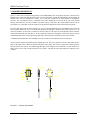
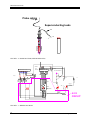
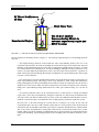
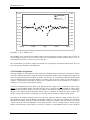
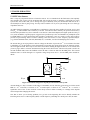
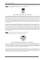
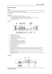
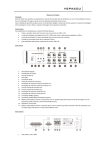
User’s Manual for the model MFP Multi-Function SQUID Probe By: Tristan Technologies,Inc. San Diego, California USA copyright 2001 Multi-Function Probe Tristan Technologies, Inc. Part Number 3000-081 Revision Record Date June 1992 February 1993 April 1993 Feb. 1995 April 1995 March 1999 January 2001 Revision A B C D E F G Description Product Release Documentation Update Documentation Update Update iMAG Documentation Update Documentation Update Added sections 4.2.2 and 5.1 2001 by Tristan Technologies, Inc. All rights reserved. No part of this manual may be reproduced, stored in a retrieval system, or transmitted in any form or by any means, electronic, mechanical, photocopying, recording, or otherwise, without prior written permission of Tristan Technologies, Inc. iMAG® is a registered trademark of Tristan Technologies. All rights reserved Tristan Technologies, Inc. reserves the right to change the functions, features, or specifications of its products at any time, without notice. Any questions or comments in regard to this product and other products from Tristan Technologies, Inc., please contact: TRISTAN TECHNOLOGIES, INC. 6350 Nancy Ridge Drive Suite 102 San Diego, CA 92121 U. S. A. Technical Support: (858) 550 Fax: (858) 550 – 2799 [email protected] http://www.tristantech.com ii - 2700 Tristan Technologies, Inc.. Multi-Function Probe TABLE OF CONTENTS 1. GENERAL INFORMATION 5 1.1 WARRANTY 5 1.2 RETURN FOR REPAIR 5 1.3 SAFETY PRECAUTIONS FOR HANDLING CRYOGENS 6 2. INTRODUCTION TO THE MODEL MFP PROBE 8 2.1 INTRODUCTION TO SQUIDS 8 2.2 PROBE DESCRIPTION 9 3. INSTALLATION 11 3.1 INSTALLING THE PROBE IN THE CRYOSTAT 11 3.2 CONNECTING THE INPUT CIRCUIT 11 3.3 COOLING THE PROBE TO LIQUID HELIUM TEMPERATURE 13 3.4 PROPER HANDLING TO PREVENT DAMAGE 14 4. OPERATING INSTRUCTIONS iii 15 4.1 MAGNETIC FIELD MEASUREMENTS 15 4.2 DC VOLTAGE AND RESISTANCE MEASUREMENTS 4.2.1 Initial Setup 4.2.2 Making a resistance measurement 4.2.2 Principles of Operation 17 17 18 2 4.3 AC RESISTANCE, SELF INDUCTANCE, AND MUTUAL INDUCTANCE MEASUREMENTS 4.3.1 Introduction 4.3.2 Principles of Operation 4.3.3 Installation and Connection of Components 4.3.4 Dual Impedance Measurements 3 3 3 3 5 5. TROUBLESHOOTING 5.1 MFP Noise Sources 6 6 Tristan Technologies, Inc. Multi-Function Probe List of Figures and Tables FIGURE 2 - 1 MODEL MFP PROBE FIGURE 2 - 2: PROBE BOTTOM (SHIELD REMOVED) FIGURE 2 - 3: WIRING DIAGRAM FIGURE 3 - 1: CRYOSTAT INSTALLATION OF THE MODEL MFP PROBE FIGURE 4 - 1 CRYOGENIC CONNECTIONS FOR MAGNETIC FIELD MEASUREMENT FIGURE 4 - 2 CRYOGENIC CONNECTIONS FOR DC VOLTAGE AND RESISTANCE MEASUREMENT TABLE 1: 30 µΩ RESISTOR DATA FIGURE 4 - 3: IV CURVE FOR NOMINAL 30 µΩ RESISTOR FIGURE 4 - 4: R∆V/∆I AND RV/I VS. T FIGURE 4 - 5: COMPONENT CONNECTION OF AC MEASUREMENT SYSTEM FIGURE 4 - 6: CRYOGENIC CONNECTIONS FOR AC MEASUREMENT FIGURE 4-5 TERMINAL BOARD WIRING FOR DUAL IMPEDANCES iv Tristan Technologies, Inc.. 9 10 10 12 16 18 19 19 2 4 5 5 Multi-Function Probe 1. GENERAL INFORMATION 1.1 WARRANTY Tristan Limited Warranty Tristan Technologies, Inc. warrants this product for a period of twelve (12) months from date of original shipment to the customer. Any part found to be defective in material or workmanship during the warranty period will be repaired or replaced without charge to the owner. Prior to returning the instrument for repair, authorization must be obtained from Tristan Technologies, Inc. or an authorized CONDUCTUS service agent. All repairs will be warranted for only the unexpired portion of the original warranty, plus the time between receipt of the instrument at TRISTAN and its return to the owner. This warranty is limited to TRISTAN’s products that are purchased directly from TRISTAN, its OEM suppliers, or its authorized sales representatives. It does not apply to damage caused by accident, misuse, fire, flood or acts of God, or from failure to properly install, operate, or maintain the product in accordance with the printed instructions provided. This warranty is in lieu of any other warranties, expressed or implied, including merchantability or fitness for purpose, which are expressly excluded. The owner agrees that TRISTAN’s liability with respect to this product shall be as set forth in this warranty, and incidental or consequential damages are expressly excluded. . 1.2 RETURN FOR REPAIR All CONDUCTUS instruments and equipment are carefully inspected and packaged at TRISTAN prior to shipment. However, if a unit is received mechanically damaged, notify the carrier and the nearest TRISTAN representative, or the factory in San Diego; California. Keep the shipping container and packing material for the carrier and insurance inspections. If the unit does not appear to be damaged but does not operate to specifications, contact the nearest TRISTAN representative or the TRISTAN factory and describe the problem in detail. Please be prepared to discuss all surrounding circumstances, including installation and connection detail. After obtaining authorization from the TRISTAN spokesperson, return the unit for repair along with a tag to it identifying yourself as the owner. Please enclose a letter describing the problem in as much detail as possible. Repacking for Return Shipment Repack the unit in its original container (if available). It is advisable to save the original crate sent by TRISTAN; however, if this is not possible, use the following instructions for repacking. 1. Wrap the unit in either “bubble wrap” or foam rubber. 2. Cover the bottom of a sturdy container with at least 3 inches of Styrofoam pellets or shredded paper. 3. Set the unit down onto the packing material and .fill the rest of the container with Styrofoam or shredded paper. The unit must be completely protected by at least 3 inches of packing material on all sides. Customers Outside of USA To avoid delays in Customs clearance of equipment being returned, contact the TRISTAN representative in your area, or the TRISTAN factory in San Diego, California, for complete shipping information and necessary customs requirements. Failure to do so can result in significant delays. Tristan Technologies, Inc. 5 Multi-Function Probe 1.3 SAFETY PRECAUTIONS FOR HANDLING CRYOGENS General Precautions The potential hazards of handling liquid helium stem mainly from the following properties: 1. The liquid is extremely cold (helium is the coldest of all cryogenic liquids). 2. The ultra-low temperature of liquid helium can condense and solidify air. 3. Very small amounts of liquid helium are converted into large volumes of gas. 4. Helium is not life supporting. Extreme Cold-- Cover Eyes and Exposed Skin Accidental contact of liquid helium or the cold gas that results from its rapid evaporation may cause a freezing injury similar to a burn. Protect your eyes and cover the skin where the possibility of contact exists. Eye protection should always be worn when transferring liquid helium. Keep Air and Other Gases Away from Liquid Helium The low temperature of liquid helium or cold gaseous helium can solidify another gas. Solidified gasses and liquid, particularly solidified air, can plug pressure-relief passages and foul relief valves. Plugged passages are hazardous because of the continual need to vent the helium gas which evolves as the liquid continuously evaporates. Therefore, always store and handle liquid helium under positive pressure and in closed systems to prevent the infiltration and solidification of air or other gases. Do not permit condensed air on transfer tubes to run down into the container opening. Keep Exterior Surfaces Clean to Prevent Combustion Atmospheric air will condense on exposed helium-cooled piping. Nitrogen, having a lower boiling point than oxygen, will evaporate first from condensed air, leaving an oxygen-enriched liquid that may drip or flow to nearby surfaces. Areas and surfaces upon which oxygen-enriched liquid can form, or come in contact with, must be cleaned to oxygen-clean standards to prevent possible ignition of grease, oil, or other combustible substances. Leak-testing solutions should be selected carefully to avoid mixtures which can leave a residue that is combustible. When combustible type foam insulations are used, they should be carefully applied to reduce the possibility of exposure to oxygen-enriched liquid which could, upon impact, cause explosive burning of the foam. Pressure-Relief Devices Must Be Adequately Sized While most cryogenic liquids require considerable heat for evaporation, liquid helium has a very low latent heat of vaporization. Consequently, it evaporates very rapidly when heat is introduced or when liquid helium is first transferred into warm or partially-cooled equipment. The quenching of a superconducting solenoid or even minor deterioration of the vacuum in the helium container can result in significant evaporation. Pressure relief devices for liquid helium equipment must, therefore, be of adequate capacity to release helium vapor resulting from such heat inputs, and thus, prevent hazard due to excessive pressure. If transfer lines can be closed off at both ends so that a cryogenic liquid or the related cold gas can become trapped between the closed ends, a pressure-relief device must be provided in that line to prevent excessive pressure buildup. Keep Equipment Area Well Ventilated Although helium is nontoxic, it can cause asphyxiation in a confined area without adequate ventilation. Any atmosphere which does not contain enough oxygen for breathing can cause dizziness, unconsciousness, or even death. Helium, being colorless, odorless, and tasteless cannot be detected by the human senses and will be inhaled normally as if it were air. Without adequate ventilation, the expanding helium can displace air and result in an 6 Tristan Technologies, Inc.. Multi-Function Probe atmosphere that is not life-supporting. The cloudy vapor that appears when liquid helium is exposed to the air is condensed moisture, not the gas itself. The issuing helium gas is invisible. Liquid containers should be stored in large, well ventilated areas. If a person becomes groggy or loses consciousness when working around helium, get them to a well ventilated area immediately. If breathing has stopped, apply artificial respiration. If a person loses consciousness, summon a physician immediately. Use of Liquid Nitrogen When liquid nitrogen is used for precooling the probe or other operations, the basic precautions given herein for handling liquid helium equally apply. Tristan Technologies, Inc. 7 Multi-Function Probe 2. INTRODUCTION TO THE MODEL MFP PROBE 2.1 INTRODUCTION TO SQUIDS The TRISTAN Model MFP Multi-Function SQUID Probe can be used to make a variety of high sensitivity laboratory measurements. As supplied, it can measure ultra-low voltages, currents, magnetic fields, resistances, and inductances. Many other physical parameters (e.g. magnetic susceptibility, position, etc.) are commonly measured with unsurpassed sensitivity using a user-supplied transducer, or input circuit, to convert the signal of interest into a current, voltage, resistance, or inductance. The word SQUID is an acronym for Superconducting QUANTUM Interference Device. For a good introduction to the construction and use of SQUID sensors, we recommend the book by O.V. Lounasmaa, Experimental Principles and Methods Below 1 K (Academic Press London and New York, 1974) or chapter 8 of Magnetic Sensors and Magnetometers (Artech House, Boston and London, 2001), and to the references therein. In its simplest form, the SQUID sensor is a sensitive detector of magnetic flux, but practical systems rarely use the SQUID to directly detect magnetic flux. The SQUID sensor contained in the Model MFP contains a tightly-coupled input coil to convert electric current into magnetic flux. The input or experimental circuit is always coupled to the SQUID via this input coil. The flux status in the SQUID sensor is measured using the TRISTAN iMAG SQUID System located at room temperature. These electronics provide a variety of functions, the most important of which are to bias the SQUID sensor and provide a feedback flux to it. This feedback is used to keep the total flux in the SQUID sensor constant. As a result, the amount of feedback flux is exactly equal to the input flux applied to the sensor. The output voltage from the electronics is a measure of the feedback flux and is therefore proportional to the input current. In terms of the flux quantum, Φ0 = 2.07 x 10⁻¹⁵ Weber = 2.07 x 10⁻⁷ gauss cm2, the current sensitivity of the input coil is approximately 2 x 10⁻⁷ A/Φ0 and the system’s output noise referenced to the input is less than 1 x 10⁻⁵ Φ0/√Hz. Exact values for these parameters may be found in the test report found in Appendix A of this manual. Using these values, you can calculate that the input circuit will resolve about 2 x 10-12 A/√Hz. The practical meaning of this value is that the rms output voltage noise of the SQUID system, measured in a one Hz bandwidth, is equivalent to a current noise at the input coil of 2 x 10-12 A (rms). If a bandwidth wider than one Hz is used to measure the noise, the rms noise will be proportional to the square root of the bandwidth. At very low frequencies, below about 1.0 Hz, the noise will be higher than this value due to a variety of factors including mechanical vibration, temperature fluctuations, flux motion, and intrinsic “1/f” noise in the SQUID sensor. The full-scale output of the system can be selected using the iMAG “GAIN” control and has a maximum value of about +500 Φ0 on GAIN= 1, 2, 5, 10, 20, 50. This implies that the experiment must be designed so that changes in the input coil current are less than + 100 µA. The SQUID only responds to changes in current and the absolute value of the current in the input coil is usually irrelevant. However, care should be taken to keep the absolute value of the current as small as practical to minimize low-frequency drift and noise. At very high values of input current, the input coil may no longer be superconducting. The features and properties discussed above apply to the use of the SQUID as a current detector. When the Model MFP probe is configured as a picovoltmeter or is used with a low-level impedance bridge, the SQUID is essentially used as a null-detector. The properties of these systems are primarily determined by other circuit parameters as discussed elsewhere. 8 Tristan Technologies, Inc.. Multi-Function Probe 2.2 PROBE DESCRIPTION Figure 2-1 shows the overall physical appearance of the Model MFP probe. In operation, the probe is inserted into a liquid helium cryostat such that the probe head is at room temperature, and the SQUID housing, which contains the SQUID sensor and low-temperature circuitry, are at 4.2K (the temperature of liquid helium at atmospheric pressure). The experimental circuit is connected to the probe through the access tube in the top of the SQUID housing. The iMAG iFL-301 Flux Locked Loop cable is always connected to the 10-pin LEMO connector on the probe head. Use of the other electrical connectors on the probe head depends on the measurement being made. The lower end of the probe is shown in Figure 2-2. Access to the ten terminals shown is obtained by unscrewing the outer niobium shield from the rest of the SQUID housing and sliding the shield off the bottom. Figure 2-3 is an electrical schematic for the probe. Terminals S1 and S2 connect to the input coil of the SQUID. These terminals, along with terminals R1, R2, M1, M2, P1, P2, P3, and P4 are mounted in a fiberglass circuit board. The use of these terminals depends on the measurement being made and is discussed in the following sections of this manual. A standard mutual inductance and a standard resistor are mounted on the underside of the circuit board. An RC circuit is installed in parallel with the SQUID input coil. This serves both as a low pass, differential mode rf filter for the input and as a shunt for internal oscillations in the sensor. This circuit is required for reliable operation and it should not be removed. The standard SQUID input circuit comprises a self inductance of 2 microH and a 15 Ohm resistor in series with a 1000 pF capacitor. This yields a 3 dB roll-off of the input signal at a frequency above 15 MHz. FIGURE 2 - 1 MODEL MFP PROBE Tristan Technologies, Inc. 9 Multi-Function Probe Probe cables Superconducting leads S1 R1 R2 P1 P3 S2 M1 M2 P2 P4 FIGURE 2 - 2: PROBE BOTTOM (SHIELD REMOVED) SWITCH Lemo Microtech 1 2 3 4 5 6 7 8 6,5 7,10 2,3 8,9 H,G J,M C,D K,L 1,4 B,E 1500 pF VOLTAGE READOUT 22 µH .47 µF 10 k .01 µF 1k 5 µF .01 µF Heater Nom 3 k 1500 pF SQUID .01 µF SQUID SIGNAL INPUT nom L µH S1 R1 R2 P1 P3 S2 M1 M2 P2 P4 3X10⁻⁵ 4.2 K CIRCUIT FIGURE 2 - 3: WIRING DIAGRAM 10 Tristan Technologies, Inc.. Multi-Function Probe 3. INSTALLATION 3.1 INSTALLING THE PROBE IN THE CRYOSTAT The Model MFP probe is designed for insertion into a liquid helium cryostat as shown in Figure 3-1. The probe should be inserted through the top of the cryostat via a quick-coupling port which seals to the shaft located directly below the probe head. This 5/8" shaft is designed to fit inside a quick-connect coupling such as Key High Vacuum Products’ Model QS-62 fitting. A rubber O-ring inside this fitting provides a gas-tight seal to the shaft. Any quickcoupling designed for a 5/8-in. (15.9-mm) diameter shaft can be used. Although this installation procedure provides a reliable, gas-tight seal, the rubber O-ring results in an unpredictable electrical connection between the probe top and cryostat. In some applications, electrical ground loop or rf interference problems exist which can be eliminated by making better electrical contact between the cryostat port and the probe shaft. In these cases, we recommend the use of a metal ferruled seal, such as those made by Swagelok. Sometimes, simply connecting a short, heavy-gauge clip lead between the probe head and cryostat is sufficient to eliminate the problem. 3.2 CONNECTING THE INPUT CIRCUIT The input circuit is connected to the probe by inserting wires through the access tube in the top of the SQUID housing and connecting them to the terminals inside the housing; see Figure 2-2. Each of the ten terminals in the low-temperature SQUID housing is a niobium terminal with a brass screw and washer. All circuit wires must be positioned underneath the brass washers so that no resistance is introduced in the superconducting circuit. WARNING The niobium terminals are relatively soft and the threads can be stripped by excessive torque on the brass screws. Wires must be stripped of insulation to make contact to the niobium terminals. We recommend the use of 0.005" solid-conductor NbTi wire, such as that supplied with the Model MFP probe. This wire is insulated with heavy Formvar insulation which can be removed by first abrading the wire with fine sandpaper and then using a chemical stripper, such as “StripXtm”. Several applications of chemical stripper may be required along with a final abrasion using sandpaper. Whenever possible, all wires in the input circuit should be run as twisted pairs to minimize stray inductance and reduce spurious pickup in the input circuit. These wires also need to be electrically shielded once they leave the SQUID housing. The level of shielding required varies greatly depending on the measurement being made, but it is always better to have too much shielding than to deal with the unpredictable results of inadequate shielding. Tristan Technologies, Inc. 11 Multi-Function Probe RF filtered feedthrus on all lines OUTPUT TRISTAN MADE IN USA 2100 Metal Dewar Case Experimental Region One or more (nested) Superconducting Shields to surround experimental region and SQUID housing FIGURE 3 - 1: CRYOSTAT INSTALLATION OF THE MODEL MFP PROBE The best approach for shielding is shown in Figure 3-1. The following important aspects of the shielding should be observed: -- The SQUID housing should be located inside the same superconducting shield as the rest of the experiment. This minimizes the need for shielding the leads from the input circuit and provides improved shielding for the SQUID housing itself. Note that even though the SQUID housing provides a very high level of attenuation of environmental noise, its built-in shielding is inadequate for many experiments. To be effective, the superconducting shielding must not have any short aspect-ratio penetrations. A good rule of thumb is that any penetrations through the shield be accomplished via a superconducting tube whose length is at least 5 times its diameter. -- The connections between the SQUID housing and the experiment should be made by twisted pairs run inside superconducting tubing. This tubing is most easily obtained by solder coating thin-walled brass tubing. Although this provides good shielding and is suitable for almost all experiments, this can result in a slight increase in the system’s white noise due to Nyquist noise (also known as Johnson noise) in the brass tubing. Pure superconducting tubing (PbSn hollow-core solder, pure Niobium tubing, etc.) can also be used. -- All electrical leads that connect to the experiment must be rf filtered prior to entering the shielded region. This is most easily accomplished by putting the experiment in a dewar having an aluminum outer wall. The rf filters can then be mounted at the top of the cryostat. No additional filters should be necessary inside the cryostat unless there is an additional source of high-frequency interference inside the cryostat. Note that ALL of the leads entering the cryostat must be rf filtered, even if they do not enter the experimental region, since they could re-radiate to other leads. If it is not possible to filter all the leads, the leads which enter the shielded experimental region must be separately shielded from the unfiltered leads. This is most easily accomplished by running these leads into the cryostat inside stainless steel, or other metallic tubing. This tubing should be grounded both at the cryostat top and at the experimental shield to obtain good rf shielding. A good design principal for the rf shielding is that it should be essentially “watertight”. 12 Tristan Technologies, Inc.. Multi-Function Probe For optimum performance, the liquid helium level should be maintained at least 1 cm above the top of the SQUID housing. All superconducting leads connecting your experiment to the components in the SQUID housing should always be immersed in helium. As the helium level drops below the top of the SQUID housing, the SQUID sensor will start to warm and performance will be degraded. The SQUID electrical characteristics will gradually change until it finally ceases to function because it is no longer superconducting. The SQUID is constructed using niobium which has a zero field critical temperature of 9.46K; however, performance degradation may begin when the SQUID temperature exceeds on 5K. Furthermore, the dc output of the system will have a temperature coefficient of at least 0.1 Φ0/K. The exact value depends on a variety of factors, including the magnetic field in which the sensor was cooled, and has a typical value of about 1 Φ0/K. This temperature coefficient of the SQUID sensor can be a serious problem in applications where dc stability is important. These undesirable effects can be limited or stopped by maintaining the SQUID housing near 4.2K even though the helium is below the indicated minimum level. Operation can be thus extended by tying copper braid to the SQUID housing, using Apiezon brand “M” grease for thermal contact, and having the copper braid extend down into the liquid helium. All superconducting leads which are not immersed in liquid must also be thermally anchored in a similar way. Another alternative is to surround the SQUID housing with a copper tube which extends down into the liquid helium. 3.3 COOLING THE PROBE TO LIQUID HELIUM TEMPERATURE The area around the terminal board must be quite dry before the probe is cooled to cryogenic temperatures. Note that water expands on freezing and, therefore, any moisture present may cause damage during cooling. The probe may either be inserted into a cryostat containing liquid helium or installed in the cryostat prior to the addition of helium. In either case, care must be taken not to get moisture inside the electrical connectors at the top of the probe. Moisture in the SQUID connector is particularly a problem since it can prevent tuning of the electronics and, hence, the use of the probe. To avoid this problem, it is a good idea to leave the iFL-301 Flux Locked Loop connected to the probe at all times. In general, it is not possible to remove the moisture using a tissue or rag. The recommended procedure is to use compressed air to dry out the connector. The probe may be cooled using any standard technique that is appropriate for the rest of your experiment. There are no specific hazards associated with this probe or its operation at cryogenic temperatures. HOWEVER, BEFORE COOLING THIS PROBE, READ THE SAFETY PRECAUTIONS FOR USE OF LIQUID HELIUM AND LIQUID NITROGEN CONTAINED AT THE BEGINNING OF THIS MANUAL. The probe may be cooled directly with liquid helium or it may be precooled using liquid nitrogen without damage to the probe. As with any other mechanical device, it is safer to cool the probe slowly than to shock cool it by rapid immersion in liquid cryogen. Although the probe is likely to survive repeated shock-cooling, there is substantial risk that something will eventually break. Tristan Technologies, Inc. 13 Multi-Function Probe 3.4 PROPER HANDLING TO PREVENT DAMAGE The SQUID sensor is relatively rugged and should provide years of reliable operation if reasonable care is taken in handling the SQUID probe. The following precautions should be taken: DO NOT DROP THE PROBE OR OTHERWISE EXPOSE THE PROBE TO SEVERE MECHANICAL SHOCK DO NOT COOL THE PROBE IF IT IS NOT THOROUGHLY DRY DO NOT EXPOSE THE INPUT COIL OR ANY OTHER LEADS CONNECTED TO THE SQUID SENSOR TO HIGH VOLTAGE OR POTENTIAL SOURCES OF STATIC ELECTRICITY DO NOT EXCEED 10 MILLIAMPS INTO THE SQUID INPUT COIL, (PERMANENT DAMAGE TO THE SQUID SENSOR MAY RESULT) . 14 Tristan Technologies, Inc.. Multi-Function Probe 4. OPERATING INSTRUCTIONS 4.1 MAGNETIC FIELD MEASUREMENTS When making magnetic field measurements, no jumpers are needed on the terminal board. The superconducting pick-up coil is connected directly to terminals S1 and S2 as shown in Figure 4-1. A superconducting coil is almost always used. We strongly recommend the use of single-conductor, Niobium Titanium (NbTi) alloy wire for most applications. This wire is readily available, mechanically reliable, and will operate in high-field applications. The diameter of the wire should be 0.005" (typically 0.0063" with Formar insulation) for most applications, but very small coils may require smaller diameter wire. Changes in the flux in the signal coil (L3) produce changes in the flux in the SQUID via the mutual inductance (M) between the signal coil and the SQUID. When connecting a pick up coil to the signal coil in the SQUID, the basic arrangement should be as shown in Figure 4-1. The signal coil in the SQUID has a self-inductance of about 2 µH . The pair of interconnecting leads (L2) should be fabricated to have a negligibly small self-inductance (<0.2 µH), but this is not always possible. Typically, non-inductively wound NbTi leads have an inductance ~ 0.3 µH/meter. The entire circuit is superconducting, and hence the total flux (Φ) threading the circuit is constant and quantized. Therefore: I * (L1 + L2 + L3) = nΦ 0 In this equation, I is the current flowing in the input circuit, Φ is the flux quantum (2.068 x 10⁻¹⁵ Weber), and n is 0 an integer. DESIGN EXAMPLE: If you design an input coil with N turns, each with cross-sectional area A, and if the magnetic field normal to these turns changes by ∆B, then ∆Φ = NA(∆B). For this example NA (∆B) = ∆I (L1 + L2 +L3) where ∆I is the current sensed by the SQUID. The current sensitivity is given In the SQUID test report (see Appendix A). The usual goal in designing the input coil is to maximize the sensitivity for a given coil area. This is accomplished by setting L1 + L2 = L3 after L2 has been minimized. Exact impedance matching is of little importance and, in general, it is better if the value of (L1 + L2) is slightly less than L3. Tristan Technologies, Inc. 15 Multi-Function Probe SQUID S1 S2 R1 M1 R2 M2 P1 P2 PICK UP P3 P4 L3 S1 S2 L2 PICK UP L1 FIGURE 4 - 1 CRYOGENIC CONNECTIONS FOR MAGNETIC FIELD MEASUREMENT As a specific example, assume a two-centimeter diameter, four-turn (close-wound) pick up coil is made from 0.005" wire. The inductance of single-turn coils made from superconducting wire is given by: 8a L = 0.004 π a ln − 2 ρ where a is the loop radius in cm, ρ is the wire radius in cm, and L is in µH. The inductance of a close-wound, multi-turn coil is proportional to the number of turns squared, so the inductance of this pick up coil is about 1.0 µH. Note that this is approximately equal to the input coil inductance, so this will provide the maximum sensitivity possible using a close-wound two-centimeter diameter coil (larger coils, of course, can be made more sensitive). If we assume that the interconnecting leads have an inductance, L2, of about 0.1 µH, we can calculate that the current change in the input circuit will be given by: ∆I = ∆B N A ∆B × 4 × 314 . × 0.012 = = 739 ∆B ( L1 + L2 + L3) . + 01 . + 2) × 10 − 6 (10 = 739 * ∆B Amp / Tesla Amp/Tesla You can calculate the noise level of the magnetometer using this equation and the equivalent input current noise of the sensor. Assuming a current noise of 1 x 10-12 A/√Hz, the equivalent field noise would be 1.3 fT/√Hz. In practice, it will be nearly impossible to achieve such a low noise level since other factors, such as Nyquist (Johnson) noise from metal pieces in your dewar or experiment, will limit the sensitivity. You can also calculate the expected output voltage for a given input signal by using the above equation along with the known transfer function (i.e. gain) of the SQUID electronics (see Appendix A). Assume that, for your system, the relevant factors given in Appendix A are 2.46 x 10⁻⁷ A/Φ0 and 3.2 Volt / Φ0 (GAIN = 100). If you are using GAIN = 10, the output of the SQUID electronics will be given by: 16 Tristan Technologies, Inc.. Multi-Function Probe ∆V = (0.1 * 1/2.46 x 10-7 ) * ∆I = 4.07 x 10⁵ ∆I = 4.07 x 105 * 739 ∆B = 3 x 10⁸ Volt/Tesla Complete rf shielding of the pick-up coil is a critical aspect of any magnetometer design since rf pick-up is often the main limit to system performance. rf noise coupling to the SQUID system is usually indicated by an erratic degradation in the height of the SQUID’s periodic transfer function. This can be observed and diagnosed by accessing the MANUAL TUNE display on the iMC-303 SQUID Controller. 4.2 DC VOLTAGE AND RESISTANCE MEASUREMENTS 4.2.1 Initial Setup To make measurements of dc voltage or dc resistance, the system is operated in the external feedback mode and uses the standard resistor built into the terminal board between terminals R1 and R2; see Figure 2-3. The unknown voltage or resistance is connected between terminals S1 and R1; see Figure 4-2, and a jumper wire is connected between terminals S2 and R2. The leads should be prepared and shielded as discussed in Section 2.2. The unknown resistance or voltage must also be rf shielded. When measuring resistance, a 4-wire approach is used: The voltage leads are connected between terminals S1 and R1, and the current leads are connected to terminals P1 and P2 (see Figure 4-2). P1 and P2 are connected by 0.005" copper leads to the round Lemo style connector on the Model MFP probe head (Pins 1 & 2 on the LEMO connector). These leads are shielded, rf filtered, and are designed to handle currents up to a maximum of 0.5 Amp. A quiet, battery-operated current source with floating (not grounded) output is usually required for supplying this current. In some applications, it may be possible to use a current supply with an ac power supply or a grounded output, but this is usually not possible due to the extra rf noise typically present on the output of such supplies. Many current sources have a large amount of high-frequency noise in their output. This is frequently large enough to prevent reliable operation of the system. In the voltage mode, this will show up as rapid jumps in the output voltage or, in the extreme case, a steady full-scale drift in the output which indicates that the feedback loop is completely inoperative. In this situation, you will observe that the SQUID’s periodic transfer function will be severely degraded or completely unobservable. The old S.H.E. model CCS Constant Current Source has a relatively noise-free stable current supply. The article “Constant-current supply of 3 ppm stability and resettability; application for a SQUID” by Levy and Greenfield, Review of Scientific Instruments, volume 50 (May) 1979 pp. 655 – 658 describe how to build a suitable current source. Even if the current source is quiet, rf pick up on the leads connected to the probe can introduce substantial rf interference. If you suspect that rf interference from the current source, or the leads connected to it, is a problem, you should observe the periodic transfer function using the Analog Output on the iMC-303 Controller rear panel. This is described in Section 3.9.6 of the iMAG SQUID System manual. First, tune the channel by pressing the TUNE Key. Then switch to the MANUAL TUNE display and observe the sinusoidal transfer function via the Analog Output BNC. The transfer function should look like a clean, steady, approximately sinusoidal signal with the current source disconnected from the probe. If it is severely degraded when the current source is connected to the probe, you can be sure that it is causing a problem. You will need to replace the current source or improve the shielding of the leads. Alternatively, you can install additional rf filtering in the output lines from the current source. To put the system into the external feedback mode of operation required for these measurements, simply put the switch on the top of the probe head into the EXTERNAL position. Tristan Technologies, Inc. 17 Multi-Function Probe The iMC-303 Controller should work in any range, but GAIN = 1 is most commonly used to obtain maximum stability and immunity to noise. The voltmeter gain is independent of the iMC-303 “GAIN” setting, since it is determined solely by passive components in the probe. Note that the output voltage as measured at the iMC-303 is NOT independent of GAIN. Voltmeter readings should only be made at the OUTPUT BNC on the Model MFP Probe. As measured here, the voltmeter gain will be about 1 x 10⁸ and the 4.5V full-scale output will correspond to about 4.5 x 10⁻⁸ V at the input. The exact value for your probe can be found in Appendix A of this manual. UNKNOWN UNKNOWN S1 S2 S1 S2 R1 M1 R1 M1 R2 M2 R2 M2 P1 P2 P1 P2 P3 P4 P3 P4 dc RESISTANCE dc VOLTAGE FIGURE 4 - 2 CRYOGENIC CONNECTIONS FOR DC VOLTAGE AND RESISTANCE MEASUREMENT Inaccurate readings will be obtained if the Analog Output BNC on the rear panel of the iMC-303 Controller is used. Although the voltage at the iMC-303 Controller is proportional to probe input voltage, it will have the wrong gain factor and it will be susceptible to ground currents and thermal emfs between the two units. The value at the iMC303 Controller will also change with GAIN. You should always use the OUTPUT connector on the probe head. Any type of voltage measuring device may be connected to the OUTPUT BNC on the Model MFP probe. A DVM, oscilloscope, or chart recorder are all acceptable. However, the input impedance of the voltmeter must be greater than 1 MΩ to obtain accurate readings. It is also important that the voltmeter not generate extremely large amounts of high-frequency noise at its input. This is rarely a problem with modern voltmeters, but it can be a problem with older DVMs and with low-cost, computerized data-acquisition systems which do not provide adequate shielding of their microprocessor. 4.2.2 Making a resistance measurement Prior to setting up a complicated experiment, it is a good idea to make a simple resistance measurement to familiarize yourself with the technique. For this example, we assume that you have the following items: ♦ ♦ ♦ Tristan PMS or MPS SQUID measurement system (and cryogenic environment) Stable constant current source (S.H.E. CCS or equivalent—see section 4.2.1) µV or nV sensitive digital voltmeter A simple µΩ resistance can be made by taking ~0.010" OHFC copper wire and coating the ends with superconducting solder, leaving about 1 cm uncoated in the middle (be sure that there is no solder in this region. Otherwise you simply have a superconducting short.). This becomes your unknown. Following Figure 4-2, attach the superconducting leads with the µΩ resistance being placed between P1 and P2. 18 Tristan Technologies, Inc.. Multi-Function Probe The constant current source is connected it to pins 1 & 2 of the user input (see Figure 2-3). Be sure that the probe toggle switch is set to EXT FEEDBACK. Tune the SQUID, and then set the gain to the x1 scale with the high pass filter set to DC and the low pass filter set to 5 Hz. Attach the voltmeter to the OUTPUT BNC on the MFP probe head. First set the current source to zero and reset the SQUID by pressing the reset button on the iMC-303 controller. Now record the voltage. Increase the current by 10 µA steps and record the output voltage at each current. Then decrease the current to zero (again in 10 µA steps recording the voltages). Now reverse the current source’s polarity and run the current to -100 µA, then again back down to zero. A typical measurement will give results that look like: Table 1: 30 µΩ resistor data 0 µA -2.3mV 0 µA 1.3mV 400mV 10 µA 28.1mV -10 µA -29.5mV 300mV 20 µA 59.1mV -20 µA -60.6mV 30 µA 90.4mV -30 µA -91.4mV 200mV 40 µA 121.2mV -40 µA -121mV 50 µA 151.9mV -50 µA -153mV 100mV 60 µA 182.6mV -60 µA -184mV 0mV 70 µA 213.6mV -70 µA -214mV 80 µA 244.4mV -80 µA -245mV -100mV 90 µA 275.1mV -90 µA -276mV 100 µA 305.6mV -100 µA -307mV -200mV 90 µA 274.9mV -90 µA -276mV -300mV 80 µA 244.1mV -80 µA -245mV 70 µA 213.5mV -70 µA -214mV -400mV 60 µA 182.6mV -60 µA -184mV -100 µA -50 µA 0 µA 50 µA 100 µA 50 µA 151.9mV -50 µA -153mV 40 µA 121.1mV -40 µA -121mV 30 µA 90.4mV -30 µA -91.3mV FIGURE 4 - 3: IV CURVE FOR NOMINAL 30 20 µA 59.4mV -20 µA -60.6mV µΩ RESISTOR 10 µA 28.6mV -10 µA -29.7mV 0 µA -2.1mV 0 µA 1.3mV The I-V curve should be straight. It is not uncommon to see a slight kink at zero, indicating a zero offset problem. If the curve shows significant slope, you may be experience (I2R) self-heating of the resistor. If the heating is enough to raise the temperature of the copper resistor above the transition temperature of the solder, the effective length of the copper resistor will increase, effectively adding additional resistance at higher currents. If the I-V curve has a quadratic shape, remove and warm up the probe to ensure that you have made the connections (according to Figure 4-2) properly. One way to calculate R is by R = V/ I. A second is to take the slope between points, R = ∆V/∆I or R [(I1 + I2)/2] = (V2 – I1)/(I2 – I1). Tristan Technologies, Inc. 19 Multi-Function Probe 35 µΩ 35 µΩ from slope 34 µΩ R = V/ I 34 µΩ 33 µΩ 33 µΩ 32 µΩ 32 µΩ 31 µΩ 31 µΩ 30 µΩ 30 µΩ 29 µΩ 29 µΩ 28 µΩ 28 µΩ 27 µΩ 27 µΩ 26 µΩ 26 µΩ 25 µΩ -100 µA 25 µΩ -50 µA 0 µA 50 µA 100 µA FIGURE 4 - 4: R∆V/∆I AND RV/I VS. T The advantage of the second (∆V/∆I) method is that it reduces the influence of offset voltages. This can easily be seen by adding a constant 10 mV to the data of Table 4-1. Calculating the resistance (from the slopes, not V/ I), shows that the value of the test resistor to be 30.8 ± 0.4 µΩ. We recommend that you perform a similar measurement prior to performing experimental measurements. This will also verify proper performance of the MFP probe. 4.2.2 Principles of Operation Referring to Figure 4-2, the feedback current is fed into the standard resistor located between terminals R1 and R2. A current is fed back such that the voltage drop between terminals R1 and R2 is equal in magnitude and opposite in sign to the voltage drop between terminals S1 and R1; and, therefore, no current flows through the SQUID signal coil. The calibration network in the probe head is set to obtain a gain of 1.00 x 10⁸ within 2%. This means that if a voltage V is applied between terminals S1 and R1, then a feedback current will be generated so as to produce a voltage of V x (1.00 x 10⁸) at the OUTPUT connector. Owing to the fundamental periodic nature of the SQUID, absolute voltages are not measured but rather voltage changes are the meaningful quantity. The initial state may have a voltage drop across terminals R1 and R2, and a current flowing through the signal coil; then, any change in the unknown voltage will produce a corresponding change in the voltage between terminals R1 and R2 such as to maintain the signal coil current constant. The absolute voltage at the OUTPUT is meaningless, you can only measure changes in voltage with this system. The voltage at the OUTPUT connector may be set to near zero when the “unknown” voltage is known to be zero. This adjustment is done using the RESET and OFFSET capabilities of the iMC-303 Controller (See the iMAG SQUID System manual). Once this is done, the OUTPUT voltage will accurately reflect the absolute value of the voltage at the input. This zero adjustment is rarely made in practice since it is usually easier to measure voltage changes from the arbitrary initial voltage. It is, however, common to use the RESET control by itself to bring the 2 Tristan Technologies, Inc.. Multi-Function Probe initial voltage to a value NEAR zero so as to maximize the range of signal changes that can be observed before output overload. The system’s slew rate, or speed at which the input voltage may change without causing unreliable readings, depends on a variety of factors including circuit noise and the amplitude of the change. Typical values for large changes are less than 1 microvolt/second. Note that transients and noise at the input contribute to this rate of change and can thus limit the maximum rate of change for your applied signal. This limit is rarely a factor since the Analog Output BNC of the Model MFP limits the observable bandwidth to a few Hz. In general, this system is not practical for the observation of high-frequency signals. The rms system noise, referred to the input, is given by: |V| < (10-13 + 2 x 10-12 R + 7.4 x 10⁻¹² /√(RT) ) V/√Hz where R is the resistance of the unknown voltage source in ohms, and T is the temperature of the source resistance in Kelvin. The first and third terms represent Johnson noise contributions. The first term is for the standard resistor mounted in the SQUID housing at 4.2 K. (Johnson noise current is given by √4 kBT R ∆f, where kB is Boltzmann’s constant and ∆f is the bandwidth.) The third term is for the unknown source resistor at temperature, T. The second term represents the equivalent voltage in the SQUID input circuit due to the SQUID’s equivalent input current noise (guaranteed to be less than 2 x 10-12 A/√Hz) flowing through the source resistance. 4.3 AC RESISTANCE, SELF INDUCTANCE, AND MUTUAL INDUCTANCE MEASUREMENTS 4.3.1 Introduction Ac measurements of resistance and inductance are possible using the standard mutual inductance built into the terminal board on the Model MFP probe. In this configuration, the SQUID serves as a null detector in a cryogenic bridge circuit. These measurements require a TRISTAN Model AUTO-BALANCE RLM BRIDGE (or equivalent). The connection of these components and a complete description of their use is included in the manuals that were supplied with the AUTO-BALANCE RLM BRIDGE. 4.3.2 Principles of Operation The unknown impedance and the secondary of the standard mutual inductance are connected in series with the SQUID signal coil. One ac signal is applied to the standard mutual inductance and another ac signal is applied to the unknown impedance. These two signals are then adjusted so that no current flows in the SQUID signal coil. The ratio of these currents is equal to the ratio of the two impedances. The standard mutual inductor has a nominal mutual inductance of 1 µH; an accurate value is given on the test report contained in Appendix A of this manual. The secondary coil of the standard mutual inductor has a self-inductance of approximately 0.25 µH. 4.3.3 Installation and Connection of Components Figure 4-3 shows the correct connection of the various electronic instruments comprising the RLM system. Note that this is nearly identical to the connections required when using the older SHE SQUID system, but the SHE MFP probe is replaced by the Tristan Model MFP probe, the Model 330 SQUID electronics are replaced by the iMAG SQUID System components, and the Bi-Phase Null Detector and RBU Bridge are replaced by the AUTOBALANCE RLM BRIDGE. Tristan Technologies, Inc. 3 Multi-Function Probe Figure 4-4 shows the wiring to the Model MFP probe when it is used for this application. The excitation leads to the unknown impedance are connected to terminals P1 and P2, and the voltage leads are connected to terminals S1 and M2. Also, a jumper wire is connected between terminals S2 and M1. The leads should be prepared and shielded as discussed in Section 2.2. The unknown impedance should also be rf shielded. If the unknown impedance is a superconducting coil, it is important that all the leads in the signal coil circuit are superconducting. Particularly in this case, the leads must be positioned directly on the niobium terminals and under the brass washers where they attach to the terminals. Referring to Figure 4-4, terminals P1 and P2 are connected to Pins 1 and 2 on the round Lemo style connector on the Model MFP probe head. These leads are shielded and rf decoupled and are designed to handle currents up to a maximum of 0.5 A. Note, however, that if these leads are connected directly to the input of the SQUID sensor, you should take care not to exceed 10 mA and to prevent any static discharge. FIGURE 4 - 5: COMPONENT CONNECTION OF AC MEASUREMENT SYSTEM. An old S.H.E. Corporation model RBU can als be used in place of the RLM Bridge. 4 Tristan Technologies, Inc.. Multi-Function Probe UNKNOWN IMPEDANCE S1 S2 R1 M1 R2 M2 P1 P2 P3 P4 FIGURE 4 - 6: CRYOGENIC CONNECTIONS FOR AC MEASUREMENT The leads connecting to the primary coil in the standard mutual inductor are available at Pins 5 and 6 on the Lemo connector. These leads are also shielded and rf filtered in the probe head; they are designed to handle currents up to 0.1 A. 4.3.4 Dual Impedance Measurements This system has the capability of performing ac impedance measurements on two unknown impedances using a single Model MFP probe. One restriction is that both impedances must be superconducting or both must be resistive. The two unknown impedances are connected in series with each other and are both in the circuit simultaneously. The excitation current is applied to one unknown at time. When the bridge circuit is in balance, no current flows in the secondary (voltage) circuit. However, both impedances contribute to system noise. This is almost always negligible and has little or no effect on the system resolution unless one impedance is significantly larger than the other. The second set of excitation leads required for the second unknown impedance are connected to terminals P3 and P4 (see Figure 4-5 which shows the terminal board wiring required). You can change between the two impedances by simply changing the Z1/Z2 switch on the AUTO-BALANCE RLM BRIDGE and rebalancing the bridge. Z2 Z1 S1 S2 R1 M1 R2 M2 P1 P2 P3 P4 OPTIONAL FIGURE 4-5 TERMINAL BOARD WIRING FOR DUAL IMPEDANCES Tristan Technologies, Inc. 5 Multi-Function Probe 5. TROUBLESHOOTING 5.1 MFP Noise Sources This is a step–by–step tutorial on how to find noise sources. It is not intended to be the final answer, but hopefully most possible noise sources will be mentioned and will provide the clues to obtaining a sufficiently low noise system. This also assumes that you are having some type of difficulty with your measurement and need to do a careful analysis of what is going wrong. You may wish to read this even if you are just starting out to see what type of problems can arise. As trouble shooting equipment, you should have at a minimum, a microvolt meter capable of resolving 10 µVDC and 100 µVAC. A chart recorder with a sensitivity of at least 1 mV/division and a relatively fast speed is also useful (a recorder with speeds that vary from 1 mm/min to 125 mm/sec is more than adequate; the higher speeds are rarely, if ever, used). In addition, a general purpose, triggered sweep oscilloscope is also recommended. A preamplifier (such as a PAR model 113) can be useful if the chart recorder or oscilloscope is not very sensitive. It may also be able to provide low pass filtering which is useful in reducing some noise sources. If a low frequency spectrum analyzer (e.g., Hewlett–Packard 3582A, Wavetek, Rockland, etc.) is available, it is ideal for identifying noise sources. We assume that you are trying either to measure voltages on the order of picovolts (10-12 V) or resistances less than a nanoOhms (10-9 Ω). Resistances can be determined by measuring the voltage drop across the unknown resistor due to an applied current. There may be some noise source that is masking the signal of interest. Let us consider that you are trying to make a resistance measurement using the circuit shown below. The Picovolt system is used in an external feedback mode, hence the feedback resistors RF and rstd which are built into the MFP probe. The external feedback creates a current through rstd to equal the voltage drop across Runknown. See the MFP probe manual for details. Output R FB V input r std Figure 5-1 Schematic Diagram of SQUID picovolt measurement system Assume that Runknown has a resistance on the order of a nanoOhm (10-9 Ω). Since the typical noise level of the model PMS is ≈ 10-13 Volts/√Hz, a resistance of 10-10 Ω would require a current of 10-13 Volts/10-10 Ω = 1 mA for a signal/noise ratio of one. 10 mA would be a more likely current in order to actually see a change in the SQUID control output when changing the current. Now that we know you are having problems, let’s go back to the beginning. We need to identify whether the interfering noise source is radio frequency (RFI) or audio frequency (including 50 or 60 Hz power line) in nature. 6 Tristan Technologies, Inc.. Multi-Function Probe Step one: Remove all experimental attachments to the model MFP probe and short the inputs (with a superconducting wire placed below the brass washers as shown in Figure 5-2 ). S1 S1 R1 M1 R2 M2 P1 P2 P3 P4 Figure 5-2 MFP Terminal Arrangement for Shorted Inputs Place the internal/external feedback switch on the MFP probe to the INT position. If you are immersing the probe directly in liquid helium, you may need to wait five minutes for the SQUID and terminal board to come into thermal equilibrium (at 4.2 K). Now measure the system noise with the voltmeter (a spectrum analyzer is preferable). The noise should be less than 10 µV peak–to–peak on the x1 range (100 µV on x10 and 1 mV on x100). You may be seeing a value much greater than 10 µV. Please remember that the SQUID transfer function is multi–valued and you may need to reset the control electronics. Whatever dc value you are observing should remain stable. If not, carefully re–read the manual and try again. If you are having problems at this point, you should call the customer service department. If you suspect (50/60 Hz) power line interference, connect the output of the model iMC-303 to the chart recorder (or an oscilloscope) set to an appropriate speed and sensitivity (1 mV/div or better). At a chart speed of ~10 cm/sec (oscilloscope time base of 2 msec/div) you should be able resolve 50/60 Hz if it is present. A preamplifier (such as the PAR 113) may be helpful if your chart recorder/oscilloscope is not sufficiently sensitive (be sure that the model iMC-303 and the preamp filter settings, if any, are wider than 50/60 Hz). Please note that the model iMC-303 output may give inaccurate readings due to potential ground currents and thermal emf’s between the model iMC-303 and the MFP probe. Use of a preamp/filter between the MFP probe voltage output and the chart recorder/oscilloscope will avoid this problem. Step two: [still using internal feedback] (assuming that step one seems OK). The MFP probe terminal board connections should look like Figure 4 - 2: S1 S1 R1 M1 R2 M2 P1 P2 P3 P4 Figure 5-3 MFP Terminal Arrangement to check current sensitivity You will want to hook up your current source to pins 1 and 2 of the USER input found on the MFP probe (see section 4.2.1 for recommended current sources). Please note that this circuit is not designed to handle large ampere currents (0.5 A maximum). If you intend to use large (1 – 200 A) currents, initially try the a low amplitude current source to give a feeling for how a low noise current supply should behave. To avoid damaging the probe, high current sources should use user-installed lines separate from the MFP probe. Again, monitor the output noise from the model iMC-303. Should the noise be excessive, the current supply is the most likely source. Check for the presence of 50/60 Hz (as described in step one). If 50/60 Hz is present, you will need to filter the inputs carefully. If the 50/60 Hz is not too large, use of a notch filter in combination with the 5 Hz filter of the model iMC-303 should suffice to reduce this to an acceptable level. Tristan Technologies, Inc. 7 Multi-Function Probe Let us assume you are using your own current source. The R1, R2 network is to reduce the current that goes through the SQUID sensor. Large currents through the SQUID sensor can trap flux in the sensor (requiring the sensor to be warmed up above 10 Kelvin) or possibly damage the SQUID. What we are interested in here is to see what type of noise sources are being coupled into the SQUID system. Now repeat the same noise analysis described in step two. If OK, go onto step three. If not, then try to determine where the noise source is. If Steps one and two were OK and you are having problems, then it is a reasonable guess that your current leads or current supply is the problem. To check the current leads, hook up the model CCS to the room temperature input. If there is no change, then your leads could be the problem. If the noise “goes away”, then your power supply may be at fault. If 50/60 Hz is the major offender, you may wish to put some sort of low pass filter at the input of the leads to remove 50/60 Hz contributions. Step three: Place an “unknown” resistor of ~ 1 mΩ (2 cm of 0.1 cm (0.040") diameter brass wire or 0.2 cm of 0.040" diameter manganin (using copper wire will give µΩ resistances) in the arrangement shown in Figure 4-2 or below. Such a “large” resistance is chosen to let you easily see the effect of a non–zero Rx—once you get a feeling for µA current changes through mΩ resistances, then you can reduce Rx with some confidence that you know what is going on. Be sure to switch the internal/external feedback switch on the MFP probe to the EXT position. S1 S1 R1 M1 R2 M2 P1 P2 P3 P4 Rx Figure 5-3 MFP Terminal Arrangement for voltage (VX = I external RX) measurements Hook the voltmeter to the voltage output of the MFP probe. Using the current source, note that a current change of 10 µA will give a change in dc voltage of ≈ 1 volt. Using the chart recorder, you should be able to generate step (or saw tooth) functions by changing the current. Note that the maximum rate (slew rate) that you can change the current is one that would give you a voltage drop of 50 nV/sec across Rx. For the ~ 1 mΩ resistor, this would be equivalent to 50 µA/sec. If you have noise sources that are slewing faster than 50 µA/sec (for a 1 mΩ resistor), the system will lose lock and you will need to hunt down and eliminate those noise sources. Even if the noise does not exceed the slew rate of the model iMC-303 electronics, the sum of the slew rate of the noise sources and the ramp rate of your current supply may exceed the equivalent of 50 nV/sec. In this case you will need to reduce your maximum ramp rate. Provided that the system can maintain “lock”, it may be possible to operate the system in the presence of significant noise. For example, using a standard Picovolt Measurement System setup as described, but with a superconducting wire replacing the unknown impedance, you might observe a 50/60 Hz component to the noise of say 40 picovolts peak–to–peak. In terms of RMS noise this is 140 times the expected system noise (0.1 picovolt/√ Hz). If you hook up your voltmeter (or chart recorder) to the output (BNC) connector on the rear of the model iMC-303 control electronics, you can utilize the model iMC-303 filters to remove high frequency components that contribute to system noise. You may be able to resolve finer changes in the output voltage of your system. It is recommended that, if you have been having troubles with resolving picovolt voltages or equivalent resistances, you use a superconducting short to quantify what the actual system noise and resolution is. Then, knowing what your system performance really is, use the actual resistance of interest. 8 Tristan Technologies, Inc.. Multi-Function Probe In general, we have found that the major problem with resolving picovolts (and equivalently pΩ) is that the experimental setup allows either RFI or 50/60 Hz noise to get into the input of the SQUID. As mentioned earlier, if you are using current leads of your own design rather than the current leads internal to the MFP probe, this is a likely spot where you could be introducing noise into the system. A check with the current source will help to spot this. There may be situations where even 100 µA of noise is sufficient to cause the system to lose lock. In this situation it is preferable to use a lower maximum current. For example, using a piece of superconducting wire (Rx = 0), setting the range of the current supply to 100 mA may give rise to excessive noise, whereas reducing the supply to 50 mA maximum will allow measurements to be made. In this case, the noise contributions are due to the current supply (on the 100 mA range). Commercially available current sources (e.g., Hewlett–Packard 6260B) may have relatively large amounts of noise and ripple (especially those designed to put out 100 A or more). If you suspect that your power supply may be introducing noise, you may want to check the current ripple and noise by measuring the voltage drop across a resistor (e.g., a Dale 1Ω, 250 W resistor). As mentioned before, you may be able to reduce these contributions by filtering. Contact the current source manufacturer for instructions on how to appropriately filter their supply. An alternative approach is to use 12V car batteries in parallel to provide large, relatively noise free, current sources. The use of battery supplies will avoid coupling 50/60 Hz into the system. You will need to have enough battery capacity such that the battery will not be loaded down and the current decrease so much that it causes voltage changes (across Rx) to exceed the system slew rate. To further reduce RF interference, you may wish to place a small resistive shunt across the input of the SQUID sensor. (Model MFP probes shipped from the factory may have a moderately low impedance (3Ω) shunt across the input of the SQUID sensor.) A 1 Ω shunt will reduce the (SQUID) frequency response to 80 kHz while raising sensor equivalent noise to 150 µΦ/√ Hz. The equivalent numbers for a ½ Ω shunt are 40 kHz and 200 µΦ/√ Hz. Fortunately, efforts to reduce 50/60 Hz also tend to reduce RFI also. Even if your power supply is perfect and your leads are well filtered, it may be possible to introduce noise into the system by ground loops or improper grounding of your power supply. How you “dress” your leads, especially if you are in a severe RFI environment, may determine if you are actually creating an antenna for noise. Tightly twisted pairs of wires tend to have low inductances and thus not to act as antennae. If your dewar is non–metallic (e.g., a G–10 fiberglass dewar such as the Tristan model BMD–6X), audio and RF interference may not be attenuated. Metal dewars can be superior in their rejection of RF noise, but only if the experiment is completely surrounded by metal (i.e., a Faraday cage). Using a metal dewar may not prevent noise from entering into your system if there are openings that are not metallic (e.g., using a rubber stopper to seal an access port or an insulating top plate to the dewar). The best way to isolate the experiment is to have it completely surrounded with a superconductor. 0.005" thick lead foil can be used for this purpose. However, remember that it does no good to use a superconducting shield if you are going to pump large quantities of RFI and 50/60 Hz down the experimental leads. What has been written is by no means a complete description on how to eliminate all noise sources from the model PMS Picovolt Measurement System. It should give you a starting point and allow you to hunt for the noise sources with some degree of confidence. Tristan Technologies, Inc. 9