
1
Implementing a PCI-Express AMBA interface
controller on a Spartan6 FPGA
Master of Science Thesis in Integrated Electronic System Design
Anandhavel Sakthivel
Chalmers University of Technology
Department of Computer Science and Engineering
Göteborg, Sweden, February 2013
The Author grants to Chalmers University of Technology and University of Gothenburg
the non-exclusive right to publish the Work electronically and in a non-commercial
purpose make it accessible on the Internet.
The Author warrants that he/she is the author to the Work, and warrants that the Work
does not contain text, pictures or other material that violates copyright law.
The Author shall, when transferring the rights of the Work to a third party (for example a
publisher or a company), acknowledge the third party about this agreement. If the Author
has signed a copyright agreement with a third party regarding the Work, the Author
warrants hereby that he/she has obtained any necessary permission from this third party to
let Chalmers University of Technology and University of Gothenburg store the Work
electronically and make it accessible on the Internet.
Implementing a PCI-Express AMBA interface controller on a Spartan6 FPGA
ANANDHAVEL SAKTHIVEL
© ANANDHAVEL SAKTHIVEL, February 2013.
Examiner: ARNE LINDE
Chalmers University of Technology
Department of Computer Science and Engineering
SE-412 96 Göteborg
Sweden
Telephone + 46 (0)31-772 1000
Cover: The cover shows Xilinx Spartan6 FPGA SP605 board
Department of Computer Science and Engineering
Göteborg, Sweden February 2013
2
Abstract
The Purpose of this Master thesis is to integrate the Xilinx PCI-Express interface core to the
GRLIB framework. Xilinx Spartan6 Endpoint block for PCI-EXPRESS is generated using
Coregen and integrated with the GRLIB framework. The design accounts for crossing clock
domains as it is inevitable in a system of chip design with multiple components running at
different frequencies. The implementation satisfies the Specification provided by AMBA and
PCI-EXPRESS. The performance and area requirement are taken into consideration and
different forms of the design is implemented in order to address it. The communication
between PC and GRLIB memory environment and the other way around is performed and
verified. Simple C codes are developed in order to initiate transfers and also to verify the
design. Debugging tools like GRMON, LSPCI and drivers provided by Xilinx are used for
analysing and verifying the design. Using GRMON the PCI-EXPRESS debug environment
could transfer data at the rate of 120 Mbits/second from PC to the memory of GRLIB. The
complete design work was carried out at Aeroflex Gaisler AB.
Keywords: AMBA, LEON3, FPGA, VHDL, Two Process Methodology, DMA, GRLIB, IP
core, PCI-EXPRESS, Xilinx, Spartan6.
3
Contents
1
2
Introduction ...................................................................................................................... 10
1.1
Background ................................................................................................................ 10
1.2
Purpose ...................................................................................................................... 10
1.3
Methodology.............................................................................................................. 10
1.4
Outline ....................................................................................................................... 10
Hardware and Software Tools .......................................................................................... 11
2.1
GRLIB ....................................................................................................................... 11
2.2
AMBA ....................................................................................................................... 11
2.3
Two-process design method ...................................................................................... 14
2.4
PCI-EXPRESS........................................................................................................... 15
2.4.1
Posted and Non-posted ....................................................................................... 15
2.4.2
PCI Configuration Space .................................................................................... 15
2.5
Development Platform ............................................................................................... 16
2.5.1
2.6
Xilinx CORE Generator Systems .............................................................................. 16
2.7
Spartan®-6 FPGA Integrated Endpoint Block for PCI Express® ............................ 17
2.7.1
Core settings for PCI Express wrapper .............................................................. 17
2.7.2
Maximum payload size ...................................................................................... 18
2.7.3
Maximum Read Request Size ............................................................................ 18
2.7.4
Read Completion Boundary ............................................................................... 18
2.7.5
Bus Mastering .................................................................................................... 19
2.7.6
Error Detection ................................................................................................... 19
2.7.7
Flow control ....................................................................................................... 19
2.8
3
Key Features ....................................................................................................... 16
Designing with the core ............................................................................................. 20
2.8.1
Receiving Packets .............................................................................................. 20
2.8.2
Receive packet throttling .................................................................................... 21
2.8.3
Transmitting Packets .......................................................................................... 22
2.8.4
Transmit source throttling .................................................................................. 23
2.8.5
Transmit Destination Throttling ......................................................................... 23
Implementation................................................................................................................. 25
3.1
Common Design techniques ...................................................................................... 25
3.1.1
Endpoint Inputs/outputs ..................................................................................... 25
3.1.2
Clock Synchronisation ....................................................................................... 25
3.2
PCI-EXPRESS Target ............................................................................................... 25
3.2.1
Core settings ....................................................................................................... 26
4
3.2.2
3.3
PCI-EXPRESS Master/Target ................................................................................... 28
3.3.1
3.4
Design Details .................................................................................................... 28
PCI-EXPRESS Master Burst Transfer (With FIFO and optional DMA) .................. 30
3.4.1
4
Design Details .................................................................................................... 27
Design Details .................................................................................................... 30
Verification....................................................................................................................... 33
4.1
Simulation.................................................................................................................. 33
4.1.1
Simulation libraries ............................................................................................ 33
4.1.2
Verification......................................................................................................... 33
4.2
Hardware Verification ............................................................................................... 34
4.2.1
PCI-EXPRESS debug interface ......................................................................... 34
4.2.2
Xilinx driver ....................................................................................................... 34
4.2.3
JTAG and Ethernet for bus mastering and burst transfers ................................. 34
5
Discussion ........................................................................................................................ 35
6
Conclusion ........................................................................................................................ 35
7
Future Work ..................................................................................................................... 36
8
References ........................................................................................................................ 37
Appendix A - Transaction Level Packets (TLPs) .................................................................... 38
5
Acknowledgement
I like to thank my supervisor Jiri Gaisler for giving this opportunity and setting up a
wonderful work environment. I like to thank the staffs of Aeroflex Gaisler AB for their
technical support and friendly behaviour towards me. Finally, I like to thank my Examiner in
Chalmers Arne Linde for his constant support throughout the thesis.
6
List of Figures
Figure 1 : Example LEON3 system designed with GRLIB [1] ................................................ 11
Figure 2 : A typical AMBA-based microcontroller [4] ............................................................ 12
Figure 3: AMBA AHB/APB conceptual view [1] ..................................................................... 12
Figure 4: AHB inter-connection view page [1] ....................................................................... 13
Figure 5 : APB inter-connection view [1] ............................................................................... 13
Figure 6 : Generic two-process circuit [5] .............................................................................. 14
Figure 7: Layering Diagram .................................................................................................... 15
Figure 8: Xilinx SP605 Board Features [2] ............................................................................ 16
Figure 9: TLP 3-DW Header without Payload [7] .................................................................. 21
Figure 10: TLP 3-DW Header with Payload [7] ..................................................................... 21
Figure 11 : User Application Throttling Receive TLP [7]....................................................... 22
Figure 12: TLP with 3-DW Header with Payload [7] ............................................................. 22
Figure 13: Source throttling on the Transmit Data path [7] ................................................... 23
Figure 14: Destination throttling on the Transmit Data path [7] ........................................... 24
Figure 15: Interfacing PCI-EXPRESS to the GRLIB............................................................... 26
Figure 16: Address translation from PCI-EXPRESS bus address to AMBA Address ............. 27
Figure 17: PCI-EXPRESS Master/Target implementation ...................................................... 28
Figure 18: Address translation from PCI-EXPRESS bus address to AMBA Address ............. 29
Figure 19: PCI-EXPRESS Master Burst Transfer implementation ......................................... 30
Figure 20: Two port sync RAM and its interface ..................................................................... 31
7
List of Tables
Table 1: BRAMS required according to performance and MPS selection .............................. 17
Table 2: Configuration dcommand [7:5] value ....................................................................... 18
Table 3 : Configuration dcommand [14:12] value .................................................................. 18
Table 4: Configuration lcommand[3] value ............................................................................ 19
Table 5: configuration dstatus register and correponding error representation .................... 19
Table 6: Available transmit buffers[7] ..................................................................................... 20
Table 7: Required BRAMS corresponding to Performance and MPS selection ...................... 26
8
Abbreviations
AHB Advanced High-performance Bus - AMBA standard bus for High-performance
AMBA Advanced Microcontroller Bus Architecture - On-Chip Communication Bus
APB Advanced Peripheral Bus - AMBA standard bus for Low-power peripherals
ASB Advanced System Bus - AMBA standard bus for High-performance
ATX Advanced Technology Extended - motherboard form factor specification
BRAM Block Random Access Memory - Type of memory used in FPGA
CPU Central Processing Unit - main component of Computer
DDR Double Data Rate - Type of memory
DMA Direct Memory Access - access system memory independent of CPU.
DW Double Word - 32 bits
FIFO First In First Out - Type of data Access
FMT Format of TLP - Specifies the TLP type
FPGA Field Programmable Gate Array - Integrated circuit configurable by User
GRLIB Gaisler Research Library - Library consist of IP cores, scripts for tools etc
GRMON Gaisler Research Debug Monitor - Debugging
GT Giga Transfer - Unit for data transfer
GUI Graphical User Interface - Used in tools for providing settings
IP Intellectual Property - Portable and reusable design cores
JTAG Joint Test Action Group - Design Interface
MB Mega Bytes - Unit for data transfer
MPS Maximum Payload Size - amount of Payload appended in a packet
PCI Peripheral Component Interconnect - Design Interface
RCB Read Completion Boundary - Value significant for receiving data
SRAM Static Random-Access Memory - type of memory
SPARC Scalable Processor Architecture - type of Architecture used by LEON Processor
SPI Serial Peripheral Interface Bus - Design Interface
TLP Transaction Level Packets - Headers and Data Packets in PCI-EXPRESS transfers
UART Universal Asynchronous Receiver/Transmitter - Design Interface
VHDL Very High Speed Integrated Circuits Hardware Description Language - Description
for defining hardware
9
1
1.1
Introduction
Background
Aeroflex Gaisler AB provides GRLIB IP Library a set of reusable IP cores freely
available in open-source. The library consists of LEON3 SPARC V8 processor, PCI, USB
host/device controllers, DDR and Ethernet interfaces etc. The library supports different
vendors, Synthesis, Simulation tools and target technologies. AMBA on-chip bus is used as
the standard communication interface between the GRLIB cores [1].
1.2
Purpose
The Purpose of this thesis is to interface the Xilinx PCI-Express interface core to the
GRLIB framework. The Xilinx PCI-Express controller is generated by the Coregen tool, and
uses hard macros on the Xilinx FPGA's. The work consists of bridging the custom interface
on the PCI-Express core with the AMBA AHB on-chip bus used in GRLIB. The PCIExpress/AMBA interface should be implemented in VHDL and assembled with the PCIExpress core. The interface is connected finally in a complete LEON3/GRLIB system. The
board is inserted on a PCI-Express slot of a PC motherboard and communication should be
made between the PC and GRLIB framework. The communication between the devices is
supported with both single and burst transfers of the AMBA. Two- Process design style is
used for implementing the entire system. This style is chosen in order to achieve the benefits
associated like efficient simulation, synthesis, maintenance, easy code analysis and
debugging[5].
1.3
Methodology
The Work splitted into study, developing specification for wrapper, implementation,
analysis and verification and carried out step by step. The study period mainly consist of
understanding the functionality of PCI-EXPRESS core, PCI-EXPRESS specifications,
AMBA specifications and understanding the GRLIB framework. After the study period the
requirements are clear and specifiations for the wrapper is developed. The implementations
are made as per the requirement, further they are analysed for improvements and verified for
proper functionality.
1.4
Outline
The Hardware and sotware tools details is provided in the section 2 , explaining about
GRLIB, AMBA plug and play, two-process design method, Xilinx Spartan6, PCI-Express
core properties and specification used, section 3 describes implementation details of PCIExpress/AMBA interface controller. Section 4 consists of details about debugging using
GRMON and verification in simulation and hardware. Section 5, 6 and 7 are Discussions,
Conclusions and Future work respectively.
10
2
Hardware and Software Tools
This chapter explains the tools used for implementing the design, hardware settings available
and designing with the Endpoint core. This chapter also explains different options available
from the tools.
2.1
GRLIB
GRLIB consist of reusable IP cores supporting different target technologies and CAD tools.
AMBA on-chip bus is used for central communication. GRLIB uses unique plug and play for
connecting different components of the system. The library is constructed to be vendor
independent. Makefiles are used to create simulation and synthesis scripts for different
vendors. Figure 1 shows an example template design with several components of a systemon-chip.
Figure 1 : Example LEON3 system designed with GRLIB [1]
Some of the Features available in GRLIB are Plug and play (the ability to detect available
system hardware through software), Distributed address decoding ( to avoid dependencies on
a global resource) and Portability ( Technology independent). For further details please refer
to GRLIB IP Library User’s Manual [1].
2.2
AMBA
GRLIB AMBA on-chip bus is in compliance with AMBA specification 2.0. Three different
buses are available as per specification Advanced High-performance Bus (AHB), Advanced
11
System Bus (ASB) and Advanced Peripheral Bus (APB). GRLIB uses AHB for high
performance and high clock frequency and APB for low power peripherals. Figure 2 shows a
typical example of AMBA and peripheral system [4].
Figure 2 : A typical AMBA-based microcontroller [4]
Figure 3 below shows how the system is divided into masters, slaves and connected through
AMBA. A single AHB slave is used to implement AHB/APB bridge. AHB slave2/APB
master represents AHB/APB bridge and it is the only APB master. By placing multiple
AHB/APB bridges several APB buses can be achieved.
Figure 3: AMBA AHB/APB conceptual view [1]
Figure 4 shows how masters and slaves are divided and controlled by a global bus control for
AHB interconnection, details about input and output signals also provided. The signals in
12
figure below are composed of record types. Details about the signals are available in GRLIB
IP Library User’s Manual [1].
Figure 4: AHB inter-connection view page [1]
Figure 5 shows APB interconnection with details about input and output signals. The signals
in figure below are composed of record types. Details about the signals are available in
GRLIB IP Library User’s Manual [1].
Figure 5 : APB inter-connection view [1]
For further details please refer to AMBA specification[4].
13
2.3
Two-process design method
The dataflow style of coding would result in difficulty for reading and understanding the code
because of numerous number of concurrent statements and processes. Low abstraction level
and longer simulation time are other difficulties associated with the dataflow method. Twoprocess coding method helps to overcome these difficulties. Meanwhile to overcome these
difficulties some simple measures like using record types in all signal declarations, twoprocesses per entity and high level sequential statements[5]. Figure 6 shows two-process
design methodology.
Figure 6 : Generic two-process circuit [5]
Only two processes combinational (asynchronous) and sequential (registers) are used. The
complete design can be coded sequential in the combinational process and sequential process
updates the state using registers.
Following advantages are achieved by two-process design methodology
•
•
•
•
•
Structured and readable VHDL code
Efficient simulation and synthesis
Easy code analyses and maintenance
Higher abstraction level
Simplified debugging and analysis
For further details please refer to two- process design documentation[5].
14
2.4
PCI-EXPRESS
PCI-EXPRESS is a computer expansion bus standard which replaces the older PCI and PCI-X
bus standards. The standard specifies the architecture in three layers which are transaction,
data link and physical layers. Figure 7 shows the layering arrangement. PCI-EXPRESS uses
packets to transfer information between devices. The packets are formed and passes along
different layers collecting additional information’s, similarly the reverse happens at the
receiving end. Some works done by layers are transaction level packets generation and
analysis, data protection, flow-control, error detection, serialization and de-serialization. The
PCI-EXPRESS is backward compatible with the existing PCI software model [6].
TX
Transaction Layer
Transaction Layer
Data Link Layer
Data Link Layer
Physical Layer
RX
TX
Physical Layer
RX
Figure 7: Layering Diagram
2.4.1
Posted and Non-posted
During write operations, the packets are formed and given to the data link layer and the write
transaction is completed. This type of transaction is Posted transaction. In read operation,
from the requester the packets are formed and given to data link layer. The requester should
wait for the respective completions. This type is non-posted transaction.
2.4.2
PCI Configuration Space
From the configuration space for PCI-EXPRESS, important registers like status, command,
device status, device control, link control and link status are given to the user application
through configuration ports. Apart from those, user application can read the complete
configuration space. The user application cannot write into the configuration space. The root
port can write and read the entire configuration space.
15
2.5
Development Platform
The template design used for this thesis is available in GRLIB which is leon3-XilinxSP605. The leon3-Xilinx-SP605 template design contains IP cores for memory interface, user
interface like JTAG, USB, Ethernet and several other components. Figure 8 below shows the
Xilinx Spartan-6 FPGA SP605 evaluation board used in this thesis. The board has PCIEXPRESS x1 edge connector (single lane) which is inserted into the PCI-Express slot of the
motherboard.
Figure 8: Xilinx SP605 Board Features [2]
2.5.1
•
•
•
•
•
•
•
•
•
Key Features
Spartan-6 FPGA XC6SLX45T-3C in FGG484 package
128 MB DDR3 memory
32 MB parallel (BPI) flash memory
8Kb IIC EEPROM
8 MB Quad SPI flash memory
10 Mb/s, 100 Mb/s, 1,000 Mb/s Ethernet
GTP transceiver port (TX, RX) with four SMA connectors
PCI Express® x1 edge connector
12V wall adapter or ATX power supply
Configuration can be performed using onboard JTAG configuration circuitry, 8 MB Quad SPI
flash memory; 32 MB Parallel (BPI) flash memory and 2 GB Compact Flash (CF) memory
card [3].
2.6
Xilinx CORE Generator Systems
Xilinx CORE Generator system helps to reduce the design time by providing
optimized intellectual properties (IP) for Xilinx FPGAs. Spartan®-6 FPGA Integrated
16
Endpoint Block for PCI Express® core is generated using Coregen and used in this design to
implement the PCI-EXPRESS/AMBA interface controller.
2.7
Spartan®-6 FPGA Integrated Endpoint Block for PCI Express®
Spartan®-6 FPGA Integrated Endpoint Block for PCI Express® core was generated using
Coregen and used in this design to implement the PCI-EXPRESS/AMBA interface controller.
2.7.1
Core settings for PCI Express wrapper
The core is configured by appropriately setting in GUI.
Device/Port type: PCI Express Endpoint device
Base Address Registers: Base Address Registers have two purposes. First it specifies the
amount of address space required for the device in the system memory map. Secondly the
BIOS or OS programmes base address registers with the assigned addresses for the device
which gives information to perform address decoding for the device. In this core there are 6
Base Address Registers available for 32 bit BARs, the address range can be as small as 128
bytes for memory or 16 bytes for I/O. 2 gigabytes is the maximum address range [7].
ID values: Vendor ID- Specifies the manufactures of the device. Identifiers are given by PCI
Special Interest Group for uniqueness.
Device ID- Identifier for the application can be any value.
Max Payload Size: The maximum data payload that can be appended along with other headers
for a write transmission. The maximum data payload can be 128, 256 or 512 bytes. The final
value for this is written in the device control registers by the BIOS. The values are explained
in section 2.7.2
BRAM configuration options: The performance level can be set to good or high based on the
amount of Header and Data credits needed for transmission. The amount of TLP buffers
needed for transmission is also depends on performance level. The BRAMs used depends on
these performance level settings as well as the Max payload size. The table 1 shows the
BRAMs requirements according to performance and MPS selection
MPS (bytes) Performance BRAMs Required
128
Good
2
High
4
256
Good
4
High
8
512
Good
8
High
18
Table 1: BRAMS required according to performance and MPS selection
17
The core supports link speed of 2.5 GT/s with width single lane (x1). The reference clock
frequency used is 125 MHz .The PCI-EXPRESS specification version 1.1 is used for building
the core.
2.7.2
Maximum payload size
The device control registers specifies amount of data which can be sent as a payload. The
root complex sets the device control registers after the link is trained, even though we
requested for a specific maximum payload size using the software GUI. The root complex
driven value can be less than or equal to the advertised capacity selected.
Configuration dcommand [7:5] signal which is available to the user application gives the
value of MPS as shown in table 2.
Configuration dcommand [7:5] MPS(bytes)
000b
128
001b
256
010b
512
Table 2: Configuration dcommand [7:5] value
2.7.3
Maximum Read Request Size
The amount of data which can be requested by the user as payload is given by the device
control registers. The root complex sets the device control registers after the link is trained,
even though we requested for a specific maximum read request size using the software GUI.
The root complex driven value can be less than or equal to the advertised capacity selected.
Configuration dcommand [14:12] signal which is available to the user application gives the
value of Maximum Read Request Size as shown in table 3.
Configuration dcommand [14:12] Maximum Read Request Size
(bytes)
000b
128
001b
256
010b
512
Table 3 : Configuration dcommand [14:12] value
2.7.4
Read Completion Boundary
The requested data can be answered with multiple completions. The number of completions
depends on the amount of data requested and Read completion boundary. Read completion
boundary value is written on the device control register Configuration lcommand (3). Table 4
shows the valve in configuration lcommand register and associated bytes value.
18
Cfg_lcommand[3] Bytes
0
64
1
128
Table 4: Configuration lcommand[3] value
The Completions are quantised in a way the payload starts and end at an aligned RCB length
except when completions of starting or ending are serviced. Detailed explanation of RCB is
given at section 3.4.1 under Multiple completions for burst read.
2.7.5
Bus Mastering
The endpoints can write and read the CPU memory directly like a Root Complex. For this the
bus master bit configuration command (2) should be enabled. This bit is enabled during the
link training. The configuration command bit is available for user application to determine
whether the bit is enabled or not. If configuration command bit is enabled then memory or
I/O requests can be generated.
2.7.6
Error Detection
The configuration dstatus is available for user application to determine the internal state of the
system. When any error conditions occurs it is reflected in the device status registers as
shown in table 5
Configuration dstatus(0) Correctable Error Detected
Configuration dstatus(1)
Non-fatal Error Detected
Configuration dstatus(2)
Fatal Error Detected
Configuration dstatus(3) Undefined Request Detected
Table 5: configuration dstatus register and correponding error representation
2.7.7
Flow control
Receive Buffer Credits
The buffers credits available in endpoints are available to the user application from the
following signals trn_fc_ph, trn_fc_pd, trn_fc_nph, trn_fc_npd, trn_fc_cplh and
trn_fc_cpld[11:0].
As per PCI-EXPRESS specification, Endpoints should advertise infinite credits available for
completions. The user application should implement logics not overflowing the available
completion credits. The completion credits reduce when a completion is received after read
request from the endpoint. The read requests have to be cautiously sent from endpoint
without emptying the completion credits and therefore producing an infinite completion
possibility.
19
Transmit Buffer
The number of available transmit buffers is given by the signal trn_tbuf_av. A single buffer
can hold a maximum sized TLP which is 4DW of headers and maximum payload size data.
The buffers are exclusive for a single transfer i.e. even if there is a single 32 bit memory read
request which needs only 3DW header that will occupy a single TLP buffer. The TLP’s are
not shared. The table 6 shows available buffers as per MPS and performance level selection
made in the GUI of Coregen.
Maximum Payload Size Performance Level
(bytes)
Good
High
128
13
27
256
14
29
512
15
30
Table 6: Available transmit buffers[7]
The trn_tbuf_av can fluctuate without any packet transmission from the user application; the
buffers are also shared with configuration management module (CMM). The configuration
management module generates completion packets when configuration writes or reads,
interrupts and message transfers occurs.
2.8
Designing with the core
The Core generated Sparan6 endpoint device has control and data transfer signals which has
to be connected to the user application. The control signals like start of frame, end of frame
should be properly given at proper timings along with data to make a successful transmission.
Below sections explain about the control and data signal interfacing with the user application.
2.8.1
Receiving Packets
For receiving a packet the headers and payload data should be available at sequences with
proper control signals asserted at right time.
The user application should assert trn_rdst_rdy_n when it is ready to accept a new packet. The
core asserts trn_rsrc_rdy_n and trn_rsof_n together and provides the initial frame on trn_td.
When final frame is sent trn_reof_n is asserted. The figures 9 and 10 shows read request and
write request respectively. The headers are described in Appendix A.
20
Figure 9: TLP 3-DW Header without Payload [7]
Figure 10: TLP 3-DW Header with Payload [7]
2.8.2
Receive packet throttling
When the user application is not ready to process incoming requests, it can throttle the
requests by deasserting trn_rdst_rdy_n. The trn_rdst_rdy_n can be deasserted for any length
of time and can be desserted any time, even during middle of a TLP reception. The figure 11
explains throttling using trn_rdst_rdy_n.
21
Figure 11 : User Application Throttling Receive TLP [7]
2.8.3
Transmitting Packets
The core assert trn_tdst_rdy_n when it is ready to accept a new packet, the user application
should asserts trn_tsrc_rdy_n and trn_tsof_n together providing the initial frame on trn_td.
During final frame trn_teof_n is asserted. The figures 12 shows a write request. The headers
are described in Appendix A.
Figure 12: TLP with 3-DW Header with Payload [7]
22
Figure 13: Source throttling on the Transmit Data path [7]
2.8.4
Transmit source throttling
The user application can throttle transmitting if it don’t have data on the consecutive clock
cycles. This is done by deasserting trn_tsrc_rdy_n as shown in figure 13.
2.8.5
Transmit Destination Throttling
When the internal transmit buffers (see section 2.7.7 for transmit buffers) are not available the
core can throttle the transmission by deasserting trn_tdst_rdy_n as shown in figure 14. The
trn_tbuf_av gives the number of buffers available for the transmission. By asserting
trn_tdst_rdy_n the core accepts start of frame and also it guarantees it will accept the entire
TLP with the Payload available in it.
23
Figure 14: Destination throttling on the Transmit Data path [7]
24
3
Implementation
This chapter explains implementation of different design versions like Target, Master and
Master with FIFO. The implementations are made with emphasis on performance and area.
The interfaces associated with AMBA are different in each designs are explained in detail.
The chapter also explains about some common design techniques followed for all the different
wrappers implemented.
3.1
Common Design techniques
Pin out I/O and timing constraints are given similar to the user constraints available in the
example design generated from Coregen, as the design constraints should exactly match the
specification given in the GUI of Coregen. The power is obtained by the DC power supply or
through 12V ATX power supply, power connections available in PCI-EXPRESS edge
connector are not used [8]. The slot clock Configuration is enabled allowing the Endpoint to
use platform provided physical reference clock available on the PCI-EXPRESS edge
connector.
3.1.1
Endpoint Inputs/outputs
The PCI-EXPRESS cores inputs and outputs are grouped according to the functions they
perform as Record types and they are listed below.
• inputs and outputs from user application
• Flow control – Gives the amount of buffers available for Posted, completions and
nonposted transactions to the user design.
• Configuration – Species the user status and command configuration of the device,
error control and interrupt handling etc.
3.1.2
Clock Synchronisation
Clock synchronisation is performed using handshaking with double stage synchronizers
which provides immunity to the possible meta-stability occurrence. The Generic nsync is set
to two for double stage synchronisation.
3.2
PCI-EXPRESS Target
The PCI-EXPRESS Target is the simplest of all the implementation using lesser hardware
resources. The design cannot perform burst transfer and it can only act as a slave to the Root
Complex. Writes or reads cannot be generated from the endpoint block. The PCI-EXPRESS
Target acts as a slave to system Root complex. It accepts the memory read and write request
from upstream components through Root complex. The Target generated completions as a
response to read requests are sent to the upstream components through Root complex. The
user application uses AHB Master Configuration to access the memory space of Leon3
system. AHB Master is interfaced along with the PCI-EXPRESS core to configure a new
master in the GRLIB system.
25
The wrapper consist of Core generated PCI-EXPRESS core and interface to the AMBA onchip bus, along with techniques like clock synchronisation and byte twisting. The
implemented design is based on the Two Process design style and Inputs and Outputs are
grouped as record types for easy debugging and implementations. The two process technique
is explained at section 2.3. The figure 15 shows different blocks of PCI-EXPRESS Target
implementation along with GRLIB components.
Figure 15: Interfacing PCI-EXPRESS to the GRLIB
3.2.1
Core settings
The Core generator can be configured to generate a Spartan6 Endpoint block with the needed
settings. The GUI from core generator tool helps to give proper settings for the core to be
generated.
Base Address Registers:
Type: Memory 32 bits (For PCIE Target only)
Size: 2 Megabytes (The base address register can be configurable through generics which can
be in the range of 128 bytes to 2 Gigabytes)
Max Payload Size: 128 bytes. BRAM configuration Performance option: Good
MPS (bytes) Performance BRAMs Required
128
Good
2
High
4
Table 7: Required BRAMS corresponding to Performance and MPS selection
26
No user configuration and extended configuration space is implemented.
Details about core settings are explained in section 2.7.1 all other settings apart from the
mentioned above are set to default.
3.2.2
Design Details
•
The user design uses clock (trn_clk) provided by the PCI-EXPRESS endpoint core
Frequency 62.5 Mhz. Similarly trn_reset from the Endpoint is used for user design
reset. When main system_reset is asserted for the endpoint or when link disabled it is
set asynchronously.
•
All top interfaces to the PCI-EXPRESS core like system clock, System reset, data
Input and outputs are channelled through this wrapper. Similarly the inputs and
outputs needed for the AMBA interface is also accessed.
•
The AMBA interface consist of reset, Clock, AHB master input and AHB master
output where these are all connected through respective signal's from the top main.
•
Byte-Twisting is performed as the PCI-EXPRESS data transfer is in big endian
format.
•
Address translation: The address space allocated for the PCI-EXPRESS memory is
divided into two halves. Access to the upper half writes AHB address register and
access to the lower half is forwarded to internal AHB access. The internal access
address is formed by taking significant part from the AHB address register and the
remaining original address provided for access. The figure 16 explains the mechanism.
Upper half access writes to the AHB address register
AHB Address[31:abits-1]
Unused (abits -2 to 0)
Lower half access the memory
AHB Address[31:abits-1]
Original Address from Root complex
Figure 16: Address translation from PCI-EXPRESS bus address to AMBA Address
The abits are made as generics in order to account if memory ranges are changed in
PCI-EXPRESS bars.
27
3.3
PCI-EXPRESS Master/Target
The PCI-EXPRESS Master/Target can act as master or slave to the AMBA, corresponding to
target or Master to the PCI-EXPRESS interface. The GRLIB system through any of its master
can generate memory request using the PCI-EXPRESS master interface, bus mastering should
be enabled to perform this communication. The figure 17 shows different blocks of PCIEXPRESS Master/Target implementation.
Figure 17: PCI-EXPRESS Master/Target implementation
The core settings are similar to PCI-EXPRESS Target implementation.
3.3.1
Design Details
The communication from root port to the GRLIB frame work remains same as explained in
section 3.2, all the techniques used like address decoding, clock synchronisation and byte
twisting remains the same. The details about ability of the core to generate memory
transaction (bus mastering) are explained below.
• The PCI-EXPRESS Master block contains the necessary logic for creating the
memory transaction level packets (TLPs). The packets are generated when AHB slave
block gets inputs from any of the masters in GRLIB framework.
28
•
The AMBA interface consist of reset, Clock, AHB slave input and AHB slave output.
The AHB slave block controls the communication with hresponse, hready and some
other signal as per AMBA Protocol.
•
The APB registers specified is used for register access associated with PCI-EXPRESS.
The PCI-EXPRESS bus address to which the memory transaction has to be performed
is given by a register PCIBA. The PCIBA can be accessed through APB and
configured with the needed address as shown in figure 18.
Figure 18: Address translation from PCI-EXPRESS bus address to AMBA Address
The width of PCIBA can be adjustable according to the generics provided in the core which is
dependent on the memory space window provided for the PCI-EXPRESS.
• The bus master bit configuration command (2) should be enabled for bus mastering.
This bit is enabled during the link training. The configuration command is available
for user application to determine whether the bit is enabled or not.
•
The availability of transmit buffer is checked before every start of transmission.
•
Endpoints are required to advertise an infinite amount of completion space which can
be achieved by sending read requests according to the available completion
buffers(applicable when Endpoint act as master)[7]. The condition is satisfied by
checking availability of completion headers before every new read request.
•
The APB access is also used for monitoring internal registers when debugging using
GRMON [9].
29
3.4
PCI-EXPRESS Master Burst Transfer (With FIFO and optional DMA)
The PCI-EXPRESS Master Burst Transfer is capable of generating burst of transfer from
GRLIB framework to the upstream root complex. The wrapper has a FIFO to act as buffers
for the transfer and an optional DMA. figure 19 depicts different blocks associated with this
design.
Figure 19: PCI-EXPRESS Master Burst Transfer implementation
3.4.1
•
•
Design Details
The core can handle burst transaction generated from GRLIB masters as well as the
normal single writes and reads. The difference between burst and single operations are
identified using hburst signal from AHB slave inputs.
The burst transfers are generated when AHB slave block gets requests from any of the
masters in GRLIB framework . The resulting datas from the burst transfer are loaded
into the FIFOs. The PCI-EXPRESS Master block contains the necessary logic for
creating the burst memory transaction level packets (TLPs) .
30
•
The DMA controller shown in figure 19 can be configured using APB interface to
start burst of transfer. The DMA registers can be configured with burst starting
address, length, destination address. After configuration when the start is asserted
burst transfer occurs. Optional interrupt can also be set to indicate end of
communication. When DMA engine is not in work the core can perform burst transfer
from other masters, the address translation for these masters are similar to the address
translation explained at section 3.3.1 (figure 18) using APB.
•
The AMBA interface consist of reset, Clock, AHB slave input and AHB slave output.
The AHB slave block controls the communication with hresponse, hready, hburst,
htrans and some other signal as per AMBA Protocol.
•
The write and read have separate FIFOs where each is split into 2 halves. Syncram 2P
Two port RAM from GRLIB is used for the FIFOs. The FIFO is of 32 (double words)
depth and separate clocks AMBA and PCI-EXPRESS clocks are used. The figure 20
shows the interfacing of FIFO which is inbetween the AMBA AHB slave and PCIEXPRESS Master.
Figure 20: Two port sync RAM and its interface
•
Burst write - As soon as first half of FIFO is fully written by AHB slave interface the
PCI-EXPRESS master empties it, at the same time AHB slave interface keeps on
writing till the second half gets filled. When the second half is also full PCIEXPRESS master empties everything in the FIFO. When these happens the access to
FIFO from AHB slave interface gets retry response.
31
•
Burst read- When AHB slave gets a read burst request it is transformed into PCIEXPRESS burst read. As soon as first half of FIFO is fully written by PCI-EXPRESS
master the AHB slave interface empties it, at the same time PCI-EXPRESS master
keep on writing to the second half. After the second half is full AHB slave interface
empties it. When AHB slave is waiting for the PCI-EXPRESS master to fill it gives
retry response.
•
Multiple completions for burst read - The number of completions received for a burst
read request is based on Read completion boundary value available in control registers
(see section 2.7.4). The core is designed for Read completion boundaries of 64 bytes.
Every burst read request is of size 128 bytes (32 DW) can be completed either with
two 64 bytes completions or 3 completions of variable payload. Two or three
completions depends on the address from which the request starts. For example a 128
byte (32 double word) address request start from 0x00000000 the completions are
received as two 64 byte (16 double words each) at 0x00000000 and 0x00000040
starting addresses. If the 128 byte (32 double word) address request start from
0x00000004, three completions are received 60 byte (15 DW), 64 byte (16 DW) and 4
byte (1 DW) at 0x00000004, 0x00000040 and 0x00000044 starting addresses.
Basically the return completions are quantized according to the Read Completion
Boundaries. The core takes care of this multiple completions using the received length
and byte count value available with the completion TLPs .
•
4k Address Crossing- The address and length of read or write request should not cross
4k address boundary as per PCI-EXPRESS specification, if this case occurs the TLPs
are not processed by the endpoint and not further pass to the root port resulting in
malfunction of the system. The core handles this by splitting the burst into before
crossing and after crossing whenever an address crossing occurs.
32
4
Verification
Logic Simulation and Hardware implementation are performed to verify the working of the
system. Modelsim is used for simulation and Xilinx Spartan6 is used for hardware
implementation. Simulation is performed with the help of simulation environment provided
by Coregen generated endpoint block for PCI-EXPRESS, AMBA test framework from
GRLIB and using the available testbench in the Xilinx SP605 template design. Hardware
analysis is assisted by Debugging tools like GRMON, LSPCI and drivers provided by Xilinx.
4.1
Simulation
The simulation environment provided along with Xilinx endpoint block is integrated to the
GRLIB framework to simulate the traffic. The simulation environment provided helps to
generate traffic from root port and accept completions associated with it. If the traffic is
generated from GRLIB (bus mastering) the simulation environment provided won’t respond
for any TLPs reaching it.
4.1.1
Simulation libraries
The complete simulation libraries needed for Modelsim environment is generated using
Xilinx ISE and stored in the PC. The Modelsim.ini file present in the template design is
modified to access the libraries needed for simulation. The secureip and unisim files already
available in GRLIB under GRLIB/lib/tech are disabled.
4.1.2
Verification
The functionality of PCI-EXPRESS target is verified by Writing to an address and reading
from the same address and comparing weather both of them are same. The other cores which
have bus mastering capability the functionality was not completely verified using simulation
as the root port don’t return any TLP’s for request from GRLIB framework. The functionality
for PCI-EXPRESS master is only verified partially by generating TLPs and checking whether
the datas are channelled through AMBA properly and send it to the PCI-EXPRESS core, the
notion of generation of TLP’s and possible answers are manually generated and verified. For
example instead of sending the read request to the upper layers of PCI-EXPRESS, the
completions are manually done and results are given and verified for correctness.
For generating simple single write and read traffic from GRLIB framework prom.s file is
modified to generate memory request. Sparc assembly is used for generating the traffic using
prom.s. Similarly while generating traffic from DMA, prom file is used for giving fetch,
destinations address, length and start. AMBA test framework is used for generating burst
transfer, the ATF is instantiated into the GRLIB framework and used for generating AMBA
burst read and write traffic.
33
4.2
Hardware Verification
The descriptions are synthesized and a bitstream is generated using Xilinx tools for testing
the system. The bitstream are flashed into the FPGA and analysed. GRMON is used as a
debug monitor for the GRLIB framework, which can be used to read/write system memory
and registers, downloading, executing LEON applications etc. The debug links like USB,
JTAG, RS232, PCI, Ethernet and Space wire are supported by GRMON.
4.2.1
PCI-EXPRESS debug interface
The software features associated with PCI is completely compatible with PCI-EXPRESS, so
the supporting features GRMON provides for PCI is available for PCI-EXPRESS as well. The
PCI-EXPRESS target can act as a debug interface for the GRLIB framework. PCI-EXPRESS
debug environment could transfer data at the rate of 120 Mbits/second from PC to the
memory of GRLIB.
4.2.2
Xilinx driver
The drivers provided by Xilinx memory endpoint test driver [refer xapp1022] is used for
simple transfer of data from PC to GRLIB framework and vice versa. The application C files
are modified to transfer from PC to GRLIB, similarly the device driver files are modified to
place a buffer memory space in the PC memory to write read and verify while bus mastering.
4.2.3
JTAG and Ethernet for bus mastering and burst transfers
Simple C codes are written in order to generate traffic. JTAG and Ethernet is used for loading
the executables into the system and execute it for transfers. The write are made followed by
reading then compared weather they are the same or not. For verifying burst transfers using
DMA similar C code giving details about fetch, destinations address, length and start is used.
The Ethernet is used for generating burst transfers, mem and bload commands in GRMON are
used in order to achieve burst transfers.
34
5
Discussion
The works specified according to the specification are implemented, verified and performance
evaluation was carried out step by step and analysed. Whenever necessary the specifications
are modified and adapted with implementations to make improvements in performance or
hardware resource utilization. The respinning was quiet time consuming as a simple change in
specifications resulted in reiteration of implementation and complete verification. The number
of versions of wrapper makes it complicated if a common specification for each design is
modified. The Two-Process design style used for implementing the system helped greatly
while simulating and analysing the design. The code is readable and can be maintained easily
because of the structured coding style resulting from two process design. The advantages
available from GRLIB in implementation, simulation and debugging are extensively utilized
to make this working module.
6
Conclusion
The purpose of this Master thesis to integrate the Xilinx PCI-Express interface core to the
GRLIB framework was fulfilled. The work is carried out with performance and area
requirement in mind. The different forms of the design is implemented in order to address for
every need. The design is made in accordance with specifications provided by AMBA and
PCI-EXPRESS. The difficulties arised like clock synchronisation,boundary crossing and tool
related issues are addressed properly and a working module is implemented on the Xilinx
Spartan6 board. Possible changes like timing and I/O contrainsts to the Xilinx SP605 GRLIB
template design is made to make the PCI-EXPRESS work along with other components of
GRLIB framework.
The board inserted into the PCI-Express slot of a PC motherboard and communication is
made between the PC and GRLIB framework and also the other way around. The
communication between devices is supported with both single and burst transfers of the
AMBA. The Example simulation environment provided with PCI-EXPRESS core helped to
verify the system using modelsim simulation. The Hardware design is verified and analysed
using drivers from Xilix and GRMON debug environment .
35
7
Future Work
The performance achieved by this design can be improved by several means. The PCIEXPRESS Master Burst Transfer which has hardcode FIFO depths, the FIFO depths can be
made variable and faster burst transfer can be achieved. Other features of PCI-EXPRESS like
interrupts can be added to this design. The unavailability of simulation response when the
PCI-EXPRESS core act as master results in complicating the implementation and through
simulation only partial verification can be achieved, this can be rectified by incorporating root
module which respond to request given by GRLIB PCI-EXPRESS Master. Further all the
cores only support word trasfers, logic can be added to support byte tranfer.
36
8
References
[1] GRLIB IP Library User’s Manual.
http://www.gaisler.com/products/grlib/grlib.pdf
Version
1.1.0
B4113
January,
[2] Xilinx SP605-Hardware Setup Guide,
http://www.xilinx.com/support/documentation/boards_and_kits/xtp089.pdf
[3] Xilinx SP605 Getting Started Guide ug525,
http://japan.xilinx.com/support/documentation/boards_and_kits/ug525.pdf
[4] AMBA Specification Revision 2.0. ARM Limited. 1999.
[5] Gaisler, J. Fault-tolerant Microprocessors for Space Applications. Gaisler Research.
[6] PCI-EXPRESS Base 1.1 Specification. PCI-SIG.
[7] Xilinx Spartan-6 FPGA Integrated Endpoint Block for PCI Express User Guide,
http://www.xilinx.com/support/documentation/user_guides/s6_pcie_ug654.pdf
[8] Xilinx SP605-Hardware Setup Guide,
http://www.xilinx.com/support/documentation/boards_and_kits/ug526.pdf
[9] GRMON User’s Manual. Version 1.1.51. Aeroflex Gaisler AB. November, 2011,
http://www.gaisler.com/doc/grmon.pdf
37
2012
Appendix A - Transaction Level Packets (TLPs)
Write TLPs
The figure below shows an example write TLP (4 DWs) which has 3 headers and a data field
using 32 bit addressing.
31
30 29
R
Fmt
28 27 26 25 24
Type
23
22 21 20
R
TC
19 18 17 16
Reserved
15
T
D
14
13 12
11 10
E
P
Attr
R
Requester ID
Tag
9
8 7
6
5
Last
DW BE
Address[31:2]
Data[31:0]
First DW:
R- Reserved
Fmt
00
01
10
11
TLP Format
No data, 3 DW header
No data, 4 DW header
3 DW header and data
4 DW header and data
FMT and TLP format
TLP
Memory Read
Memory Write
I/O Read
I/O Write
Completion
Fmt
00 or 01
10 or 11
00
10
10
Type
00000
00000
00010
00010
01010
FMT and type for respective TLPs
Fmt and Type field together indicates whether it is a Read, Write or completion TLP.
TC - Traffic class
TD - Presence of TLP digest at the end of TLP is indicated by setting this bit 1b.
EP – Indicates Poisoned TLP
Length – Indicates the data payload length in DWs.
38
4
3
2
1
0
Length
First DW
BE
R
Second DW:
Requester ID
Bus Number Device Number Function Number
7:0
4:0
2:0
Used for reporting back errors during write but significant during reads.
Tag -No significance during writes
First DW BE - Indicates which four bytes are significant in the first DW of the data payload
Last DW BE - Indicates which four bytes are significant in the last DW of the data payload
Third DW: Contains 30 most significant address bits and 2 reserved bits which should be
zero.
Fourth DW: Single DW of data.
Read TLPs
The figure below shows an example read TLP (3 DWs).
31
30 29
R
Fmt
28 27 26 25 24
Type
23
22 21 20
R
TC
19 18 17 16
Reserved
15
T
D
14
13 12
11 10
E
P
Attr
R
Requester ID
Tag
9
8 7
6
5
4
3
2
0
Length
Last
DW BE
Address[31:2]
First DW
BE
R
The Read TLP request is similar to the write TLP with few differences. Only the differences
are discussed below.
Second DW :
The Requester Id specifies where to send the completion of a read request.
Tag – This field can be given any value but it is useful for the requester to keep track of the
completions coming back.
Completion TLP
The figure below shows an example Completion TLP (4 DWs) which has 3 headers and a
data field using 32 bit addressing.
39
1
31
30 29
R
Fmt
28 27 26 25 24
Type
23
22 21 20
R
TC
Completer ID
Requester ID
19 18 17 16
15
14
13 12
Reserved
T
E Attr
D P
Completion B
Status
C
M
Tag
Data[31:0]
11 10
R
9
8 7
6
5 4
3
2
Length
Byte Count
R Lower Address
The First DW is similar to read/write request.
Second DW:
Completer Id - sender of the packet
Completion status – Indicates completion status
BCM- Set by PCI-X completers not set by PCI-EXPRESS completers.
Byte count- The amount of bytes pending for transmission including the available data in the
current payload, useful if multiple completions are expected.
Third DW:
Requester ID and Tag – similar to read request
Lower Address – least seven bits of the requested address.
40
1
0


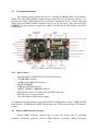


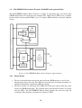


![E^YB?= ce``_bd VY\Uc V_b @QbQTYW] 4UReW BD](http://vs1.manualzilla.com/store/data/005839928_1-81490c34e940fa2480ecad1c81f1b8b0-150x150.png)