1
A1SQN
A1SQN-E
USER’S MANUAL
Revision 1.0a
The information in this user’s manual has been carefully reviewed and is believed to be accurate.
The vendor assumes no responsibility for any inaccuracies that may be contained in this document,
and makes no commitment to update or to keep current the information in this manual, or to notify
any person or organization of the updates. Please Note: For the most up-to-date version of this
manual, please see our website at www.supermicro.com.
Super Micro Computer, Inc. ("Supermicro") reserves the right to make changes to the product
described in this manual at any time and without notice. This product, including software and documentation, is the property of Supermicro and/or its licensors, and is supplied only under a license.
Any use or reproduction of this product is not allowed, except as expressly permitted by the terms
of said license.
IN NO EVENT WILL SUPER MICRO COMPUTER, INC. BE LIABLE FOR DIRECT, INDIRECT,
SPECIAL, INCIDENTAL, SPECULATIVE OR CONSEQUENTIAL DAMAGES ARISING FROM THE
USE OR INABILITY TO USE THIS PRODUCT OR DOCUMENTATION, EVEN IF ADVISED OF
THE POSSIBILITY OF SUCH DAMAGES. IN PARTICULAR, SUPER MICRO COMPUTER, INC.
SHALL NOT HAVE LIABILITY FOR ANY HARDWARE, SOFTWARE, OR DATA STORED OR USED
WITH THE PRODUCT, INCLUDING THE COSTS OF REPAIRING, REPLACING, INTEGRATING,
INSTALLING OR RECOVERING SUCH HARDWARE, SOFTWARE, OR DATA.
Any disputes arising between the manufacturer and the customer shall be governed by the laws of
Santa Clara County in the State of California, USA. The State of California, County of Santa Clara
shall be the exclusive venue for the resolution of any such disputes. Supermicro's total liability for
all claims will not exceed the price paid for the hardware product.
FCC Statement: This equipment has been tested and found to comply with the limits for a Class
A digital device pursuant to Part 15 of the FCC Rules. These limits are designed to provide
reasonable protection against harmful interference when the equipment is operated in a commercial
environment. This equipment generates, uses, and can radiate radio frequency energy and, if not
installed and used in accordance with the manufacturer’s instruction manual, may cause harmful
interference with radio communications. Operation of this equipment in a residential area is likely
to cause harmful interference, in which case you will be required to correct the interference at your
own expense.
California Best Management Practices Regulations for Perchlorate Materials: This Perchlorate
warning applies only to products containing CR (Manganese Dioxide) Lithium coin cells. “Perchlorate
Material-special handling may apply. See www.dtsc.ca.gov/hazardouswaste/perchlorate”.
WARNING: Handling of lead solder materials used in this
product may expose you to lead, a chemical known to
the State of California to cause birth defects and other
reproductive harm.
Manual Revision: 1.0a
Release Date: April 28, 2015
Unless you request and receive written permission from Super Micro Computer, Inc., you may not
copy any part of this document.
Information in this document is subject to change without notice. Other products and companies
referred to herein are trademarks or registered trademarks of their respective companies or mark
holders.
Copyright © 2015 by Super Micro Computer, Inc.
All rights reserved.
Printed in the United States of America
Preface
Preface
This manual is written for system integrators, IT technicians and
knowledgeable end users. It provides information for the installation and use of the
A1SQN/A1SQN-E motherboard.
About This Motherboard
The
A1SQN/A1SQN-E motherboard supports a small core and low power
Intel® Quark™ X1021 SoC (System-on-a-Chip) processor in a BGA package. With
a X1021 processor built in, the A1SQN/A1SQN-E motherboard offers thermally
constrained, fanless, and headless applications with security and manageability
features. The A1SQN/A1SQN-E is ideally suited for the Internet of Things (IoT)
Gateway connecting devices to the cloud. This motherboard is a platform that enables companies to seamlessly interconnect industrial infrastructure devices and
secure data flow between devices and the cloud. Please refer to our website at
http://www.supermicro.com/products/ for processor and memory support updates.
This product is intended to be installed and serviced by professional technicians.
Manual Organization
Chapter 1 describes the features, specifications and performance of the motherboard, and provides detailed information on the Intel® X1021 processor.
Chapter 2 provides hardware installation instructions. Read this chapter when installing the processor, memory modules and other hardware components into the
system. If you encounter any problems, see Chapter 3, which describes troubleshooting procedures for mini PCIe card.
iii
A1SQN/A1SQN-E Motherboard User's Manual
Conventions Used in the Manual:
Special attention should be given to the following symbols for proper installation and
to prevent damage done to the components or injury to yourself:
Warning: Critical information to prevent damage to the components or injury to yourself.
Important: Important information given to ensure proper system installation or to relay safety precautions.
Note: Additional Information given to differentiate various models or to
provide instructions for correct system setup.
iv
Contacting Supermicro
Contacting Supermicro
Headquarters
Address:
Super Micro Computer, Inc.
980 Rock Ave.
San Jose, CA 95131 U.S.A.
Tel:
+1 (408) 503-8000
Fax:
+1 (408) 503-8008
Email:
[email protected] (General Information)
[email protected] (Technical Support)
Web Site:
www.supermicro.com
Europe
Address:
Super Micro Computer B.V.
Het Sterrenbeeld 28, 5215 ML
's-Hertogenbosch, The Netherlands
Tel:
+31 (0) 73-6400390
Fax:
+31 (0) 73-6416525
Email:
[email protected] (General Information)
[email protected] (Technical Support)
[email protected] (Customer Support)
Web Site:
www.supermicro.nl
Asia-Pacific
Address:
Super Micro Computer, Inc.
3F, No. 150, Jian 1st Rd.
Zhonghe Dist., New Taipei City 235
Taiwan (R.O.C)
Tel:
+886-(2) 8226-3990
Fax:
+886-(2) 8226-3992
Email:
[email protected]
Web Site:
www.supermicro.com.tw
v
A1SQN/A1SQN-E Motherboard User's Manual
Table of Contents
Preface
About This Motherboard................................................................................................. iii
Manual Organization...................................................................................................... iii
Conventions Used in the Manual:..................................................................................iv
Contacting Supermicro....................................................................................................v
Chapter 1 Introduction
1-1Overview.......................................................................................................... 1-1
Checklist........................................................................................................... 1-1
Motherboard Features...................................................................................... 1-5
1-2
Processor Overview ........................................................................................ 1-7
Chapter 2 Installation
2-1
Standardized Warning Statements.................................................................. 2-1
Battery Handling............................................................................................... 2-1
Product Disposal.............................................................................................. 2-3
2-2 Static-Sensitive Devices................................................................................... 2-4
Precautions...................................................................................................... 2-4
Unpacking........................................................................................................ 2-4
2-3 Motherboard Installation................................................................................... 2-5
Tools Needed................................................................................................... 2-5
Location of Mounting Holes............................................................................. 2-5
Installing the Motherboard............................................................................... 2-6
2-4
Connectors/IO Ports......................................................................................... 2-7
Backplane I/O Panel........................................................................................ 2-7
Ethernet Ports............................................................................................. 2-8
Universal Serial Bus (USB)......................................................................... 2-9
Serial Port.................................................................................................... 2-9
Hardware Reset Button............................................................................. 2-10
RTC Battery Connector............................................................................. 2-10
5V-18V Motherboard Power Connector.....................................................2-11
Alternative Power Connector.................................................................... 2-12
I2C Connector............................................................................................ 2-13
SPI Flash Program Header....................................................................... 2-13
A1SQN/A1SQN-E 2X10 External I/O Conector........................................ 2-14
JP5V and JP3V3 Jumpers........................................................................ 2-14
Micro SD Card Slot................................................................................... 2-15
Mini PCIe Card Slots................................................................................. 2-15
ZigBee Headers........................................................................................ 2-16
vi
Table of Contents
JTAG Header ........................................................................................... 2-17
2-5
LED Indicators................................................................................................ 2-18
Micro SD Read/Write Indicator (LED7)..................................................... 2-18
Chapter 3 Troubleshooting
3-1
Technical Support Procedures......................................................................... 3-1
3-2
Frequently Asked Question.............................................................................. 3-2
3-3
Returning Merchandise for Service................................................................. 3-3
vii
A1SQN/A1SQN-E Motherboard User's Manual
Notes
viii
Chapter 1: Introduction
Chapter 1
Introduction
1-1Overview
Checklist
Congratulations on purchasing your computer motherboard from an acknowledged
leader in the industry. Supermicro boards are designed with the utmost attention to
detail to provide you with the highest standards in quality and performance.
Please check that the following items have all been included with your motherboard.
If anything listed here is damaged or missing, contact your retailer.
The following items are included in the retail box:
•One (1) Supermicro Motherboard
•One (1) Quick Reference Guide
Note: For your system to work properly, please follow the links below to
download all necessary drivers/utilities and the user's manual for your
motherboard.
SMCI product manuals: http://www.supermicro.com/support/manuals/
Product Drivers and utilities: ftp://ftp.supermicro.com/
If you have any questions, please contact our support team at support@supermicro.
com.
1-1
A1SQN/A1SQN-E Motherboard User’s Manual
A1SQN Motherboard Image
Note: All graphics shown in this manual were based upon the latest PCB Revision
available at the time of publishing of the manual. The motherboard you've received
may or may not look exactly the same as the graphics shown in this manual.
1-2
Chapter 1: Introduction
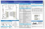
A1SQN/A1SQN-E Motherboard Quick Reference
JPWR1
J11
LAN1
LAN0
JUIDB1
JUIDB1 USB1
JIN1
USB1
JPWR1
JIN1
J11
JZB1
LAN1
JZB2
JZB1
LAN0
JBAT1
JBAT1
J12
J12
JPE1
JPE2
A1SQN REV:1.02
JPE1
JPE2
JP5V
JP5V
BAR CODE
JTAG
J1
JZB2
MAC CODE
DESIGNED IN USA
JP3V3
JP3V3
LED7
JP3
J102
JIO1
COM1
JIO1
JP3
LED7
J102
COM1
1-3
A1SQN/A1SQN-E Motherboard User’s Manual
Headers/Connectors
Connector
Description
COM1
COM1 Port
J1
JTAG Header
J11
USB Type B Port
J12
I2C Header
J102
Micro SD Card Slot
JBAT1
RTC Battery Connector
JIN1
Alternative Power Input when DC Jack is not in use
JIO1
2X10 External I/O
JP3V3
JIO1 3.3V Output (See page 2-13 for settings)
JP5V
JIO1 5V Output (See page 2-13 for settings)
JP3
2x4 SPI Flash Image Programming Header
JPE1
Full/Half Length Mini PCIe Card Slot with one USB 2.0 Interface
JPE2
Half Length Mini PCIe Card Slot
JPWR1
5V-18V Motherboard Power connector
JUIDB1
H/W Reset Button
JZB1/JZB2
ZigBee Headers
LAN0
10/100Mb Ethernet Port
LAN1
General Software program to Bridge LAN Port
USB1
USB 2.0 Port
LED
Description
LED Indicators
LED7
Color
MicroSD Read/Write Indicator
Green
1-4
Status
On
Chapter 1: Introduction
Motherboard Features
CPU
Intel® Quark™ X1021 single-core 32nm SoC (System-ona-Chip) with a clock rate of up to 400 MHz.
Memory
Onboard 512MB of DDR3-800
Network Connections
Network Controllers
Intel® X1021
LAN Ports
One (1) 10/100Mb Ethernet Port
One (1) Bridge LAN Port
I/O Devices
PCI Express Slots
One (1) Full/Half Length Mini PCIe card slot with one
USB 2.0 Interface
One (1) Half Length Mini PCIe card slot
USB Devices
One (1) USB Type A port
One (1) USB Type B port
Serial (COM) Port
One (1) RS232 Serial Port through DB9 connector
Terminal Block Connector
One (1) 2 x 10 External I/O support DIO/ADC/RS485
Memory Slot
One (1) MicroSD slot
Other
ROHS (Full Compliance, Lead Free)
A1SQN: Operating Temperature 00-600C
A1SQN-E: Operating Temperature -200-750C
Dimensions
4'' x 4.1'' (101.6mm x 104.14mm)
Optimizied for use in a NUC Chassis
1-5
A1SQN/A1SQN-E Motherboard User’s Manual
A1SQN/A1SQN-E Motherboard Block Diagram
2X4 Header
DB-9
SPI Flash 8M
Bootloader
Legacy SPI
MicroSD Slot
SD/eMMC
RS-232 XCVR
TX/RX
USB Device
Type -A
USB 2.0
10/100
Base T PHY
RJ-45
10/100
Base T PHY
JTAG Debug
Header
DDR3 X8 256MB Rank 0
DDR3 X8 256MB Rank 1
X1021
UART #0
RS-485 XCVR
Half Duplex
SPI #1
ZigBee Module
Header
SPI #0
ADC, 8Channel,
12-bit
PCIe
Half Length Mini
PCIe
Dual 10/100
Ethernet MAC
DIO/PWM
8 Channel
TPM
X2
X8
Full/Half Length Mini
PCIe
PCIe/USB Host
JTAG/ITP
EEPROM
X16
Intel QUARK
UART #1
Type -B
RJ-45
DDR3
X8
2X10 Terminal Block Socket
System Block Diagram
Note: This is a general block diagram and may not exactly represent
the features on your motherboard. See the Motherboard Features
pages for the actual specifications of each motherboard.
1-6
Chapter 1: Introduction
1-2 Processor Overview
The Intel® Quark™ SoC X1021 processor is the next generation secure, low-power
Intel® Architecture (IA) SoC for deeply embedded applications. The SoC integrates
the Intel® Quark™ SoC X1021 Core plus all the required hardware components
to run off-the-shelf operating systems and to leverage the vast x86 software ecosystem.
To enable secure applications, the SoC secures SKU features an on-die Boot ROM
that is used to establish a hardware Root of Trust (RoT). The immutable code
located within the Boot ROM is used to initiate an iterative firmware authentication
process ensuring only trusted code is executed when taking the platform out of
reset. In addition, the SoC provides an ECC-protected DRAM solution using only
standard x8 DDR3 devices.
The SoC also features a 512 Kbyte on-die embedded SRAM (eSRAM) that can
be configured to overlay regions of DRAM to provide low latency access to critical
portions of system memory. For robustness, the contents of this on-die eSRAM are
also ECC protected.
Intel® Quark™ X1021 Processor Features
The X1021 processor offers the following features:
•One-fifth the size of an Intel® Atom™ Single Core
•Simplicity and Power of Pentium Class Instruction Set Architecture Extended
Temperature qualified for Harsh, 400 MHz operating frequency
•Integrated on-die ECC support re-uses main memory to save on cost Native
PCI Express Gen 2 for differentiated I/O expansion and Architectural Scalability
•Built-in dual 10/100Mb dual LAN controller
•Built-in RS232, GPIO and I2C peripheral
•Support SDHC up to 32GB
•Two mini PCIe devices
1-7
A1SQN/A1SQN-E Motherboard User’s Manual
Notes
1-8
Chapter 2: Installation
Chapter 2
Installation
2-1 Standardized Warning Statements
The following statements are industry-standard warnings, provided to warn the user
of situations which have the potential for bodily injury. Should you have questions or
experience difficulty, contact Supermicro's Technical Support department for assistance. Only certified technicians should attempt to install or configure components.
Read this section in its entirety before installing or configuring components in the
Supermicro chassis.
Battery Handling
Warning!
There is a danger of explosion if the battery is replaced incorrectly. Replace the
battery only with the same or equivalent type recommended by the manufacturer.
Dispose of used batteries according to the manufacturer's instructions
電池の取り扱い
電池交換が正しく行われなかった場合、破裂の危険性があります。交換する電池はメー
カーが推奨する型、
または同等のものを使用下さい。使用済電池は製造元の指示に従
って処分して下さい。
警告
电池更换不当会有爆炸危险。请只使用同类电池或制造商推荐的功能相当的电池更
换原有电池。请按制造商的说明处理废旧电池。
警告
電池更換不當會有爆炸危險。請使用製造商建議之相同或功能相當的電池更換原有
電池。請按照製造商的說明指示處理廢棄舊電池。
Warnung
Bei Einsetzen einer falschen Batterie besteht Explosionsgefahr. Ersetzen Sie die
Batterie nur durch den gleichen oder vom Hersteller empfohlenen Batterietyp.
Entsorgen Sie die benutzten Batterien nach den Anweisungen des Herstellers.
2-1
A1SQN/A1SQN-E Motherboard User’s Manual
Attention
Danger d'explosion si la pile n'est pas remplacée correctement. Ne la remplacer
que par une pile de type semblable ou équivalent, recommandée par le fabricant.
Jeter les piles usagées conformément aux instructions du fabricant.
¡Advertencia!
Existe peligro de explosión si la batería se reemplaza de manera incorrecta. Reemplazar la batería exclusivamente con el mismo tipo o el equivalente recomendado por el fabricante. Desechar las baterías gastadas según las instrucciones
del fabricante.
!אזהרה
יש להחליף.קיימת סכנת פיצוץ של הסוללה במידה והוחלפה בדרך לא תקינה
.את הסוללה בסוג התואם מחברת יצרן מומלצת
.סילוק הסוללות המשומשות יש לבצע לפי הוראות היצרן
هناك خطر من انفجار في حالة اسحبذال البطارية بطريقة غير صحيحة فعليل
اسحبذال البطارية
فقط بنفس النىع أو ما يعادلها مما أوصث به الشرمة المصنعة
جخلص من البطاريات المسحعملة وفقا لحعليمات الشرمة الصانعة
경고!
배터리가 올바르게 교체되지 않으면 폭발의 위험이 있습니다. 기존 배터리와 동일
하거나 제조사에서 권장하는 동등한 종류의 배터리로만 교체해야 합니다. 제조사
의 안내에 따라 사용된 배터리를 처리하여 주십시오.
Waarschuwing
Er is ontploffingsgevaar indien de batterij verkeerd vervangen wordt. Vervang de
batterij slechts met hetzelfde of een equivalent type die door de fabrikant aanbevolen wordt. Gebruikte batterijen dienen overeenkomstig fabrieksvoorschriften
afgevoerd te worden.
2-2
Chapter 2: Installation
Product Disposal
Warning!
Ultimate disposal of this product should be handled according to all national laws
and regulations.
製品の廃棄
この製品を廃棄処分する場合、国の関係する全ての法律・条例に従い処理する必要が
あります。
警告
本产品的废弃处理应根据所有国家的法律和规章进行。
警告
本產品的廢棄處理應根據所有國家的法律和規章進行。
Warnung
Die Entsorgung dieses Produkts sollte gemäß allen Bestimmungen und Gesetzen
des Landes erfolgen.
¡Advertencia!
Al deshacerse por completo de este producto debe seguir todas las leyes y reglamentos nacionales.
Attention
La mise au rebut ou le recyclage de ce produit sont généralement soumis à des
lois et/ou directives de respect de l'environnement. Renseignez-vous auprès de
l'organisme compétent.
סילוק המוצר
!אזהרה
.סילוק סופי של מוצר זה חייב להיות בהתאם להנחיות וחוקי המדינה
2-3
A1SQN/A1SQN-E Motherboard User’s Manual
عند التخلص النهائي من هذا المنتج ينبغي التعامل معه وفقا لجميع القىانين واللىائح الىطنية
경고!
이 제품은 해당 국가의 관련 법규 및 규정에 따라 폐기되어야 합니다.
Waarschuwing
De uiteindelijke verwijdering van dit product dient te geschieden in overeenstemming
met alle nationale wetten en reglementen.
2-2 Static-Sensitive Devices
Electrostatic-Discharge (ESD) can damage electronic components. To avoid damaging your system board, it is important to handle it very carefully. The following
measures are generally sufficient to protect your equipment from ESD.
Precautions
• Use a grounded wrist strap designed to prevent static discharge.
• Touch a grounded metal object before removing the board from the antistatic
bag.
• Handle the board by its edges only; do not touch its components, peripheral
chips, memory modules or gold contacts.
• When handling chips or modules, avoid touching their pins.
• Put the motherboard and peripherals back into their antistatic bags when not in
use.
• For grounding purposes, make sure your computer chassis provides excellent
conductivity between the power supply, the case, the mounting fasteners and
the motherboard.
• Use only the correct type of onboard CMOS battery. Do not install the onboard
battery upside down to avoid possible explosion.
Unpacking
The motherboard is shipped in antistatic packaging to avoid static damage. When
unpacking the board, make sure that the person handling it is static protected.
2-4
Chapter 2: Installation
2-3 Motherboard Installation
All motherboards have standard mounting holes to fit different types of chassis.
Make sure that the locations of all the mounting holes for both motherboard and
chassis match. Although a chassis may have both plastic and metal mounting fasteners, metal ones are highly recommended because they ground the motherboard
to the chassis. Make sure that the metal standoffs click in or are screwed in tightly.
Then use a screwdriver to secure the motherboard onto the motherboard tray.
Tools Needed
Philips Screwdriver
(1)
Philips Screws (6)
Standoffs (6)
Only if Needed
JUIDB1
Location of Mounting Holes
JIN1
USB1
JPWR1
J1
JZB2
J11
JZB1
LAN1
LAN0
JBAT1
J12
JPE1
A1SQN REV:1.02
JPE2
BAR CODE
JP5V
MAC CODE
DESIGNED IN USA
JP3V3
LED7
JP3
J102
JIO1
COM1
Caution: 1) To avoid damaging the motherboard and its components, please do
not use a force greater than 8 lb/inch on each mounting screw during motherboard
installation. 2) Some components are very close to the mounting holes. Please take
precautionary measures to avoid damaging these components when installing the
motherboard to the chassis.
2-5
A1SQN/A1SQN-E Motherboard User’s Manual
Installing the Motherboard
1. Locate the mounting holes on the motherboard. (See the previous page.)
2. Locate the matching mounting holes on the chassis. Align the mounting holes
on the motherboard against the mounting holes on the chassis.
LAN0
LAN1
USB
DEVICE
USB
HOST
RESET
-
+
5~18V DC
3. Install standoffs in the chassis as needed.
4. Install the motherboard into the chassis carefully to avoid damaging other
motherboard components.
5. Using the Phillips screwdriver, insert a Phillips head #6 screw into a mounting
hole on the motherboard and its matching mounting hole on the chassis.
6. Repeat Step 5 to insert #6 screws into all mounting holes.
7. Make sure that the motherboard is securely placed in the chassis.
Note: Images displayed are for illustration only. Your chassis or components might look different from those shown in this manual.
2-6
Chapter 2: Installation
2-4 Connectors/IO Ports
The I/O ports are color coded in conformance with the industry standards. See the
figure below for the colors and locations of the various I/O ports.
Backplane I/O Panel
A
F
E
D
G
JUIDB1
C
JIN1
JPWR1
B
USB1
J1
JZB2
J11
JZB1
LAN1
LAN0
JBAT1
J12
JPE1
A1SQN REV:1.02
JPE2
BAR CODE
JP5V
MAC CODE
DESIGNED IN USA
JP3V3
LED7
JP3
JIO1
COM1
Backplane I/O Panel
A. 5V-18V Power Connector
E. USB Type B Port
B. Alternative Power Connector
F. LAN1
C. Hardware Reset Button
G. LAN0
D. USB 2.0 Port
2-7
J102
A1SQN/A1SQN-E Motherboard User’s Manual
Ethernet Ports
RJ45
Pin Definitions
One 10/100Mbps Ethernet port (LAN0)
is located on the backpanel to provide
Pin#
network connections. LAN1 is a Bridge
LAN port. These ports accept RJ45
type cables.
Definition
1
ETH_MDI_TXP
2
ETH_MDI_TXN
3
ETH_MDI_RXP
4
N/C
5
N/C
6
ETH_MDI_RXN
7
N/C
8
N/C
RJ45 PCB Pin Definition
Pin
Pin
Definition
Pin
Definition
R1
Definition
ETH_MDI_TXP
L1
LAN_ACTION_LED
C1
Chassis Ground
R2
ETH_MDI_TXN
L2
P3V3
C2
Chassis Ground
R3
TX_CT
L3
LAN_LINK_LED
R4
GND
L4
P3V3
R5
GND
R6
RX_CT
R7
ETH_MDI_TXP
R8
ETH_MDI_RXN
B
A
JUIDB1
A. LAN0
B. LAN1
JIN1
USB1
JPWR1
J1
JZB2
J11
JZB1
LAN1
LAN0
JBAT1
J12
JPE1
A1SQN REV:1.02
JPE2
BAR CODE
JP5V
MAC CODE
DESIGNED IN USA
JP3V3
LED7
JP3
JIO1
COM1
2-8
J102
Chapter 2: Installation
Universal Serial Bus (USB)
USB 2.0 Port
Pin Definitions
One Universal Serial Bus 2.0 port is located
on the I/O backpanel. A USB Type B port is
Pin#
located next to the USB 2.0 port. Cables are
not included in the shipment. See the tables
on the right for pin definitions.
Definition
1
P5V_USB
2
USB_CON_N0
3
USB_CON_P0
4
GND
USB Type B Port
Pin Definitions
Pin#
1
NC
2
USB_CON_N0
3
USB_CON_P0
4
GND
Serial (COM1) Ports
Pin Definitions
Serial Port
COM1 port is located on the backpanel
to provde a serial port connection. See
the table on the right for pin definitions.
Pin # Definition
Definition
NC
6
NC
2
RXD
7
NC
3
TXD
8
NC
4
NC
9
NC
5
NC
10
N/A
JUIDB1
A. USB 2.0 Port
B. USB Type B Port
JIN1
USB1
JPWR1
Pin #
1
B
A
J1
JZB2
C. COM1 Port
J11
JZB1
LAN1
LAN0
JBAT1
J12
JPE1
JPE2
A1SQN REV:1.02
Definition
BAR CODE
JP5V
MAC CODE
DESIGNED IN USA
JP3V3
LED7
JP3
JIO1
COM1
C
2-9
J102
A1SQN/A1SQN-E Motherboard User’s Manual
Hardware Reset Button
A Hardware Reset button is located at JUIDB1 on the backpanel next to the USB
port. When you press the reset button, the whole unit will reboot.
RTC Battery Connector
The RTC (Real Time Clock) battery connector is located at JBAT1. Use this connector to connect an RTC battery to retain system time and date. The RTC battery
is also know as a CMOS battery.
A. Hardware Reset Switch
B. RTC Battery Connector
JUIDB1
A
JIN1
USB1
JPWR1
J1
JZB2
J11
JZB1
LAN1
LAN0
B
JBAT1
J12
JPE1
A1SQN REV:1.02
JPE2
BAR CODE
JP5V
MAC CODE
DESIGNED IN USA
JP3V3
LED7
JP3
JIO1
COM1
2-10
J102
Chapter 2: Installation
5V-18V Motherboard Power Connector
5V-18V Power Connector
Pin Definitions
The 5V-18V power connector (JPWR1)
is used to provide power to the mother-
Pin#
board. This connector has a special lock
mechanism. See the images below for the
dimensions of the connector. Dimensions
are in millimeters
A
1
VIN
2
GND
3
NC
JUIDB1
A. 5V-18V Power Connector
JIN1
USB1
JPWR1
J1
JZB2
J11
JZB1
LAN1
LAN0
JBAT1
J12
JPE1
JPE2
A1SQN REV:1.02
Definition
BAR CODE
JP5V
MAC CODE
DESIGNED IN USA
JP3V3
LED7
JP3
JIO1
COM1
2-11
J102
A1SQN/A1SQN-E Motherboard User’s Manual
Alternative Power Connector
Use this alternative power connector located at JIN1 for 5V-18V input power when
DC jack is not in use. This motherboard
also supports a mating connector that can
be connected to JIN1. See the table on the
right for pin definitions of the alternative
power connector. See the images below
for the dimensions of the mating connector.
Dimensions are in millimeters.
Note: The following is the compatible mating connector product
model name: P/N: 239-02-10111-2. You can order this connector from PONY Technology Corp.
JUIDB1
A
JIN1
USB1
JPWR1
J1
JZB2
J11
JZB1
LAN1
LAN0
JBAT1
J12
JPE1
A1SQN REV:1.02
JPE2
BAR CODE
JP5V
MAC CODE
DESIGNED IN USA
JP3V3
LED7
JP3
J102
JIO1
COM1
2-12
Alternative Power Connector
Pin Definitions
Pin#
Definition
1
PVIN
2
Ground
Chapter 2: Installation
I2C Connector
I2C Header
Pin Definitions
The I C header at J12, is a 3-pin
connector, pitch 2.54mm, controls
2
Pin#
and monitors the I2C slave devices.
See the table on the right for pin
definitions.
Definition
1
SCL
2
GND
3
SDA
SPI Flash Program Header
Pin Definitions
SPI Flash Program Header
The SPI Flash header at JP3 is a 2 x 4 pin
connector, pitch 2.54mm, that can be used
to update the 8MB flash image. See the
table on the right for pin definitions.
Pin#
A. I2C Header
1
VCC
2
GND
3
CS#
4
CLK
5
MISO
6
MOSI
7
NC
8
NC
JUIDB1
B. SPI Flash Header
Definition
JIN1
USB1
JPWR1
J1
JZB2
J11
JZB1
LAN1
J12
LAN0
JBAT1
A
JPE1
A1SQN REV:1.02
JPE2
BAR CODE
JP5V
MAC CODE
DESIGNED IN USA
JP3
JP3V3
LED7
B
JIO1
COM1
2-13
J102
A1SQN/A1SQN-E Motherboard User’s Manual
A1SQN/A1SQN-E 2X10 External I/O Conector
The external I/O connector at JIO1 provides RS485, analog input, and DIO (Digital
Input/Output) connectivity. See the tables below for pin definitions.
A1SQN/A1SQN-E 2X10 External I/O
Pin Definitions
Pin#
Definition
Pin #
Definition
1
RS485A
2
RS485B
3
GND
4
GND
5
DIO1
6
DIO0
7
DIO3
8
DIO2
9
DIO5
10
DIO4
11
DIO7
12
DIO6
13
ADC1
14
ADC0
15
ADC3
16
ADC2
17
ADC5
18
ADC4
19
ADC7/3.3V
20
ADC6/5V
JP5V and JP3V3 Jumpers
JP5V provides 5V output, and JP3V3 provides 3.3V output for the external I/O
connector at JIO1. See the tables below for jumper settings.
JP5V Jumper Settings
JP3V3 Jumper Settings
A1SQN/ A1SQN-E
Pin#
Definition
A1SQN/ A1SQN-E
Pin#
Definition
1-2
JIO1 Pin 20 5V Output
1-2
JIO1 Pin 19 3.3V Output
2-3 (Default)
JIO1 Pin 20 ADC6
2-3 (Default)
JIO1 Pin 19 ADC7
Note: Please refer to page 1-3 for the locations of the external I/O connector
JIO1 and jumpers JP5V and JP3V3.
2-14
Chapter 2: Installation
Micro SD Card Slot
Insert a Micro SD memory card into the expansion slot at J102 for additional
memory or OS image.
Mini PCIe Card Slots
One Full/Half and one Half length mini PCIe card slots are located at JPE1 and
JPE2. A USB 2.0 interface is available with JPE1.
A. MicroSD Card Slot
JUIDB1
B. Mini PCIe Card Slots
JIN1
USB1
JPWR1
J1
JZB2
J11
JZB1
LAN1
LAN0
JBAT1
J12
JPE1
B
A1SQN REV:1.02
JPE2
BAR CODE
JP5V
MAC CODE
DESIGNED IN USA
JP3V3
LED7
JP3
J102
JIO1
COM1
A
2-15
A1SQN/A1SQN-E Motherboard User’s Manual
ZigBee Headers
Connect a ZigBee module to the JZB1 and JZB2 headers. The ZigBee module
allows your system to communicate to other devices through a wireless personal
area network based on 802.15.4 standard. See the tables below for pin definitions.
ZigBee Header (JZB2)
Pin Definitions
Pin#
Definition
Pin#
Definition
1
FRAME-GND
1
GND
2
RSVD1
2
VCC
3
RSVD2
3
CS1-GP5
4
RSVD3
4
RST-N-GP4
5
CS0-GP7
5
ID0-GP0
6
CLK
6
ID1-GP1
7
MOSI
7
ID2-GP2
8
MISO
8
ID3-GP3
9
VCC
9
RSVD-GP6
10
GND
10
FRAME-GND
A. JZB1
B. JZB2
JUIDB1
ZigBee Header (JZB1)
Pin Definitions
JIN1
USB1
JPWR1
J1
JZB2
B
A
J11
JZB1
LAN1
LAN0
JBAT1
J12
JPE1
A1SQN REV:1.02
JPE2
BAR CODE
JP5V
MAC CODE
DESIGNED IN USA
JP3V3
LED7
JP3
JIO1
COM1
2-16
J102
Chapter 2: Installation
JTAG Header
JTAG Header
Pin Definitions
JTAG at J1 stands for Joint Test Action
Group, a 2 x 4 pin connector, pitch 2.54mm,
is the common name for the IEEE 1149.1 Standard Test Access Port and BoundaryScan Architecture. This feature was initially
created to test printed circuit boards. See
the table on the right for pin definitions.
Pin#
Definition
1
VCC
2
TMS
3
GND
4
TCK
5
GND
6
TDO
7
N/A
8
TDI
9
GND
10
RESET
JUIDB1
A. JTAG Header
JIN1
USB1
JPWR1
J1
JZB2
J11
JZB1
A
LAN1
LAN0
JBAT1
J12
JPE1
A1SQN REV:1.02
JPE2
BAR CODE
JP5V
MAC CODE
DESIGNED IN USA
JP3V3
LED7
JP3
JIO1
COM1
2-17
J102
A1SQN/A1SQN-E Motherboard User’s Manual
2-5 LED Indicators
Micro SD Read/Write Indicator (LED7)
Micro SD Read/Write Indicator
Activity LED
The Micro SD Read/Write indicator is located at LED7. This indicator displays the
Micro SD slot activity. Refer to the table
on the right for details. Also see the layout
below for the LED location.
Color
Status
Green
On
Definition
Read/Write
JUIDB1
A. Micro SD Indicator LED
JIN1
USB1
JPWR1
J1
JZB2
J11
JZB1
LAN1
LAN0
JBAT1
J12
JPE1
A1SQN REV:1.02
JPE2
BAR CODE
JP5V
MAC CODE
DESIGNED IN USA
A
LED7
JP3
JIO1
COM1
2-18
JP3V3
J102
Chapter 3: Troubleshooting
Chapter 3
Troubleshooting
3-1 Technical Support Procedures
Before contacting Technical Support, please make sure that you have followed all
the steps listed below. Also, Note that as a motherboard manufacturer, Supermicro
does not sell directly to end users, so it is best to first check with your distributor or
reseller for troubleshooting services. They should know of any possible problem(s)
with the specific system configuration that was sold to you.
1. Please go through the ‘Troubleshooting Procedures’ and 'Frequently Asked
Question' (FAQ) sections in this chapter or see the FAQs on our website (http://
www.supermicro.com/support/faqs/) before contacting Technical Support.
2. OS image upgrades can be downloaded from our website at:
(http://www.supermicro.com/products/motherboard/quark/a1sqn.cfm), under
the link Download OS Image.
3. If you've followed the instructions above to troubleshoot your system, and still
cannot resolve the problem, then contact Supermicro's technical support and
provide them with the following information:
•Motherboard model and PCB revision number
•System configuration
•An example of a Technical Support form is on our website at:
(http://www.supermicro.com/RmaForm/).
4. Distributors: For immediate assistance, please have your account number
ready when placing a call to our technical support department. We can be
reached by e-mail at [email protected], by phone at: (408) 503-8000,
option 2, or by fax at (408) 503-8019.
3-1
A1SQN/A1SQN-E Motherboard User’s Manual
3-2 Frequently Asked Question
Question: How much memory does my motherboard support?
Answer: The A1SQN/A1SQN-E motherboard has 512MB of DDR3 800 MHz onboard memory.
Question: What kind of devices does my motherboard support?
Answer: The A1SQN/A1SQN-E motherboard supports a dual-band ZigBee module
(SMC P/N: AOC-WPAN-Q58) and mini PCIe support for wifi/Bluetooth (SMC P/N:
AOC-WLAN-NB159H) and 3G card (SMC P/N: AOC-3GMODEM).
Question: Which mini PCIe slot should I use for a 3G card?
Answer: A 3G card requires USB 2.0 interface and connects to JPE1 mini PCIe slot.
Question: Which mini PCIe slot should I use for a wifi/Bluetooth card?
Answer: Please connect the wifi/Bluetooth card to JPE1 mini PCIe slot, since a
Bluetooth device requires USB interface. JPE2 mini PCIe slot does not support
USB interface.
3-2
Chapter 3: Troubleshooting
3-3 Returning Merchandise for Service
A receipt or copy of your invoice marked with the date of purchase is required
before any warranty service will be rendered. You can obtain service by calling
your vendor for a Returned Merchandise Authorization (RMA) number. For faster
service, you may also obtain RMA authorizations online (http://www.supermicro.
com/RmaForm/). When you return the motherboard to the manufacturer, the RMA
number should be prominently displayed on the outside of the shipping carton, and
mailed prepaid or hand-carried. Shipping and handling charges will be applied for
all orders that must be mailed when service is complete.
This warranty only covers normal consumer use and does not cover damages
incurred in shipping or from failure due to the alteration, misuse, abuse or improper
maintenance of products.
During the warranty period, contact your distributor first for any product problems.
3-3
A1SQN/A1SQN-E Motherboard User’s Manual
Notes
3-4
(Disclaimer Continued)
The products sold by Supermicro are not intended for and will not be used in life support systems,
medical equipment, nuclear facilities or systems, aircraft, aircraft devices, aircraft/emergency communication devices or other critical systems whose failure to perform be reasonably expected to result
in significant injury or loss of life or catastrophic property damage. Accordingly, Supermicro disclaims
any and all liability, and should buyer use or sell such products for use in such ultra-hazardous applications, it does so entirely at its own risk. Furthermore, buyer agrees to fully indemnify, defend
and hold Supermicro harmless for and against any and all claims, demands, actions, litigation, and
proceedings of any kind arising out of or related to such ultra-hazardous use or sale.