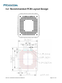
1
Copyright
Copyright ©2015 Fibocom Wireless Inc . All rights reserved.
Without the prior written permission of the copyright holder, any company or individual is prohibited to
excerpt, copy any part of or the entire document, or transmit the document in any form.
Attention
The document is subject to update from time to time owing to the product version upgrade or other
reasons. Unless otherwise specified, the document only serves as the user guide. All the statements,
information and suggestions contained in the document do not constitute any explicit or implicit
guarantee.
Trademark
The trademark is registered and owned by Fibocom Wireless Inc.
Versions
Version
Date
Remarks
V1.0.0
2014-10-17
Initial Version
V1.0.1
2014-11-24
Update the related specifications of bands
1.Change the definition of SIM2/ MMC(SDIO) pin to GND;
V1.0.2
2014-12-15
2.Update the related circuit and description of SIM1_CD and
POWER_ON/OFF.
1. Update the module appearance and power on/off timing diagram.
2. Modify the capacitance of SIM_DATA
3. Update the consumption, RF indicator and sensitivity
4. Modify the reset value of BODY_SAR and IPC_WAKEUP_HOST to
V1.0.3
2015-02-06
PU.
5. Add the high-low range of voltage and the description of unused pin
design.
Modify the format : add a space behind of the “Band”, change the
format of “LTE FDD”and “FDD LTE” to “LTE FDD”, change the format of
L810-GL LGA Module Hardware User Manual
Page 2 of 49