1
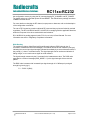
Radiocrafts
Embedded Wireless Solutions
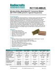
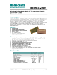
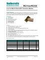
RC11xx-RC232
Low Cost Multi-Channel RF Transceiver Module
Product Description
The RC11XX-RC232 RF Transceiver Modules are compact surface-mounted high performance
modules for FSK operation with embedded protocol. The modules are completely shielded and
pre-certified for operation under the European radio regulations for license-free use.
Applications
OEM equipment
Radio modems
Alarm and security systems
Point-of-sales terminals
Bar code scanners
Telemetry stations
Fleet management
Features
Very small module (12.7 x 25.4 x 3.3 mm)
Very low sleep current consumption
Embedded RC232™ protocol with Addressing and Error check
128 byte data buffer
Two-wire UART interface for easy RS232/422/485 wire replacement (handshake optional)
Compact shielded module for SMD mounting
No external components
No configuration required for single-channel use
Easy to use data interface
Wide supply voltage range, 2.0 – 3.6 V
RC1140/80-RC232 conforms with EU R&TTE directive (EN 300 220, EN 301 489, EN 60950)
RC1190-RC232 conforms with regulations for operation under FCC CFR 47 part 15
Quick Reference Data
Parameter
RC1140-RC232
Frequency bands
Number of channels
Data rate
Max output power
Sensitivity
Supply voltage
Current consumption, RX /
TX
Current consumption, SLEEP
Temperature range
2008 Radiocrafts AS
RC1190-RC232
Unit
433.05 – 433.79
17
1.2 - 100
9
-110
2.0 – 3.6
24 / 35
RC1180RC232
868.0 – 870.0
16
1.2 - 100
9
-110
2.0 – 3.6
24 / 37
902 – 915
50
1.2 - 100
-1
-110
2.0 – 3.6
24 / 37
MHz
Typ. 0.3
-40 to +85
Typ 0.3
-40 to +85
Typ 0.3
-40 to +85
uA
C
RC11xx-RC232 Data Sheet (rev. 1.30)
kbit/s
dBm
dBm
Volt
mA
Page 1 of 22
Radiocrafts
Embedded Wireless Solutions
RC11xx-RC232
Typical application circuit
2.0 – 3.6 V
Optional
{
To host meter or
RS232/422/485
driver
GND
CTS
RTS
CONFIG
TXD
RXD
GND
GND
VCC
RESET
NC
GND
RF
GND
Antenna
NC
See page 19 for additional schematic information regarding recommended Reset and Power
supply filtering, and how to include a firmware upgrade connector.
Quick Product Introduction
How do I transmit data?
Send your data to the RXD pin on the module. Use the UART format with settings (19200, 8, 1,
N, no flow control). Up to 128 bytes are buffered in the module. The module will transmit the data
when
the max packet length is reached
the unique end character is sent
the modem timeout limit is reached
The packet length, end character and timeout limit are configurable in-circuit.
How do I receive data?
Any received data packet with correct address and check sum will be sent on the TXD pin using
the same UART format as for transmit.
What about the antenna?
In most cases a simple quarter wavelength wire or a PCB track will do. Connect a piece of wire to
the RF pin with length corresponding to the quarter of a wavelength. For space limited products,
contact Radiocrafts and we will recommend the best antenna solution for your application.
How do I change the RF channel or any other parameter?
To change configurable parameters, assert the CONFIG pin, and send the command string using
the same serial interface as for transmitting data. Parameters can be changed permanently and
stored in non-volatile memory in the module.
RCTools
RCTools is a powerful and easy to use PC suite that helps you during test, development and
deployment of the RC11XX-RC232. Visit www.radiocrafts.com for a free download and full
documentation.
2008 Radiocrafts AS
RC11xx-RC232 Data Sheet (rev. 1.30)
Page 2 of 22
Radiocrafts
Embedded Wireless Solutions
RC11xx-RC232
Pin Assignment
30
GND
29
28
27
26
25
24
23
1
14
GND
CTS/RXTX
2
13
VCC
RTS/SLEEP
3
12
CONFIG
4
11
TXD
5
10
RXD
6
9
GND
7
8
15
16
17
18
19
20
21
RESET
NC
GND
RF
GND
22
Pin Description
Pin no Pin name
1
GND
Description
System ground
2
UART Clear to Send or UART
RXTX
UART Request to Send. Set low
to enter Sleep mode if RTS
handshake is not in use.
Configuration Enable. Active low.
Should normally be set high.
UART TX Data
UART RX Data.
3
CTS/RXTX
RTS/SLEEP
4
CONFIG
5
6
TXD
RXD
Equivalent circuit
GND
VCC
Input:
20k
VCC
Output:
Use external max 8k2 kohm pullup resistor if connected to an
open collector output from a host
MCU or other high impedance
circuitry like level shifters.
7
8
GND
GND
2008 Radiocrafts AS
System ground
System ground
RC11xx-RC232 Data Sheet (rev. 1.30)
GND
Page 3 of 22
Radiocrafts
Embedded Wireless Solutions
9
RF
RC11xx-RC232
RF I/O connection to antenna
RF
10k
10
GND
System ground
11
12
NC
RESET
Not connected
Main reset (active low). Should
normally be left open. Internal 12
kΩ pull-up resistor.
GND
VCC
12k
RESET
13
VCC
Supply voltage input. Internally
regulated.
1.8 V
VREG
VCC
2u2
14
GND
System ground
15-22
RESERVED
23-30
RESERVED
Test pins or pins reserved for
future use. Do not connect!
Test pins or pins reserved for
future use. Do not connect!
GND
Note 1: For UART communication the TXD and RXD are used for serial data, and CTS and RTS for flow control
(optional). RXD should be high when not sending data to the module.
Note 2: The internal pull-ups on CONFIG and RTS/SLEEP pin are disabled in Sleep mode to minimise the sleep current.
2008 Radiocrafts AS
RC11xx-RC232 Data Sheet (rev. 1.30)
Page 4 of 22
Radiocrafts
Embedded Wireless Solutions
RC11xx-RC232
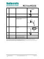
Block Diagram
GND
GND
Voltage Regulator
CTS
RTS
Communication
controller
RESET
NC
CONFIG
TXD
VCC
RF Transceiver
GND
RXD
RF
GND
GND
Circuit Description
The module contains a communication controller with embedded RC232™ protocol software, a
high performance RF transceiver and an internal voltage regulator.
The communication controller handles the radio packet protocol, the UART interface and controls
the RF transceiver. Data to be sent by the host is received at the RXD pin and buffered in the
communication controller. The data packet is then assembled with preamble, start-of-frame
delimiter (SOF), address information and CRC check sum before it is transmitted on RF. The
preamble and SOF is always used. The address and CRC are optional.
The RF transceiver modulates the data to be transmitted on RF frequency, and demodulates data
that are received.
Received data are checked for correct address and CRC by the communication controller. If the
address matches the modules own address, and no CRC errors were detected, the data packet is
sent to the host on the TXD line after removing the header.
The asynchronous UART interface consists of RXD and TXD. Optionally CTS, RTS can be used
for hardware handshake flow control. RXTX can be used to control the direction of an RS485
driver circuit.
When the CONFIG pin is asserted the communication controller interprets data received on the
RXD pin as configuration commands. There are commands to change the radio channel, the
output power, the destination address etc. Permanent changes of the configuration is also
possible and are then stored in internal non-volatile memory.
The RF protocol and the configuration commands are described in detail in the RC232™ User
Manual.
The supply voltage is connected to the VCC pin. The module contains an internal voltage
regulator and can therefore operate over a wide supply voltage range.
2008 Radiocrafts AS
RC11xx-RC232 Data Sheet (rev. 1.30)
Page 5 of 22
Radiocrafts
Embedded Wireless Solutions
RC11xx-RC232
RC232™ Embedded Protocol
The module offers a buffered packet radio in the RC232™ embedded protocol. Using the
buffered packet radio mode, all data to be sent is stored in the module before they are transmitted
by the RF circuitry. Likewise, when data is received they are stored in the module before they are
sent to the host. This allows the communication controller to add address information and to do
error check of the data. In buffered mode the UART interface is used to communicate with the
host.
The embedded protocol, configuration commands and configuration memory is described in the
RC232™ User Manual. This protocol is used in a wide range of RF modules available from
Radiocrafts. Please refer to the latest revision available on Radiocrafts web-site.
Power Management
The module can be set in SLEEP mode in order to reduce the power consumption.
The low power SLEEP mode is entered by using the SLEEP command in Configuration mode, or
by pulling RTS/SLEEP pin low. In sleep mode the module will not receive or detect incoming
data, neither from the host (UART port) nor from the RF transceiver. The module is awakened
from the SLEEP mode by a positive edge on the CONFIG pins if the module was set in SLEEP
mode using the „Z‟ command. The module is awakened by a positive edge on the RTS/SLEEP
pin if this pin were used to enter SLEEP mode. CONFIG must be high when awakening the
module to avoid setting the module directly in configuration mode. UART data on RXD to the
module should be avoided in sleep mode.
All configuration settings and RAM values are retained during Sleep. The pull-ups on RTS/SLEEP
and CONFIG pin are disabled during sleep mode in order to minimise the sleep current
consumption.
If the module is shut completely off, all configuration settings in non-volatile memory is restored,
but values in RAM are overwritten with default settings.
Enter SLEEP Mode Using RTS/SLEEP pin
RTS/SLEEP
MODE
IDLE
SLEEP
IDLE
Enter SLEEP Mode Using CONFIG and Z Comand
CONFIG
UART Comand
MODE
2008 Radiocrafts AS
Z
IDLE
CONFIG
SLEEP
RC11xx-RC232 Data Sheet (rev. 1.30)
IDLE
Page 6 of 22
Radiocrafts
Embedded Wireless Solutions
RC11xx-RC232
Timing Information
The figure and table below shows the timing information for the module when changing between
different operating states.
The IDLE state is the normal state where the module search for preamble on the air and wait for
a character to be received on the UART. RXD is the state when receiving characters from the
host filling up the internal buffer. TX state is when the data is transmitted on the air. RX state is
when data is received from the air after preamble detection. TXD is the state where the received
data is sent to the host on the UART.
CONFIG is the state entered by asserting the CONFIG pin and used during parameter
configuration, while MEMORY CONFIG is the sub-state entered by the „M‟ command where the
configuration memory is being programmed. Note the limitation on maximum number of write
cycles using the „M‟ command, see Electrical Specifications.
tTXD
tTXD-IDLE
tRX-TXD
RX
IDLE
TXD
Preamble detected
First character on
UART TXD
tRXD-CTS
IDLE
RXD
First character on
UART RXD
2008 Radiocrafts AS
tPACKET_TIMEOUT
IDLE
Last character on
UART TXD
tTX
tTX-IDLE
tRXD-TX
TX
IDLE
Last character on
UART RXD
RC11xx-RC232 Data Sheet (rev. 1.30)
Page 7 of 22
Radiocrafts
Embedded Wireless Solutions
RC11xx-RC232
tOFF-IDLE
OFF
IDLE
tRESET-IDLE
RESET
IDLE
tSLEEP-IDLE
SLEEP
IDLE
tCONFIG-PROMPT
IDLE
tC-CONFIG
CONFIG
MEMORY CONFIG
’M’
Symbol
tRX-TXD
Value
180 us
tTXD
Min 590 us
tTXD-IDLE
900 us
TRXD-CTS
20 us
tRXD-TX
960 us
TTX-IDLE
960 us
tOFF-IDLE
tRESET-IDLE
tSLEEP-IDLE
tCONFIG-
3.2 ms
3.0 ms
1.28 ms
590 us
IDLE
’X’
’C’
CONFIG
set low
CONFIG
tCONFIG-IDLE
CONFIG
tCONFIG-IDLE
tMEMORY-CONFIG
CONFIG
0xFF
IDLE
’X’
Description / Note
Time from last byte is received from the air until first character is sent
on the UART
tTXD = # bytes received x 590 us/char (10 bits at 19.2 kBd + 70 us
delay per character)
Time from last character is sent on the UART until module is in IDLE
mode (ready for RXD and RX)
Time from last character is received by the UART (including any
timeout) until CTS is activated
Time from last character is received by the UART (including any
timeout) until the module sends the first byte on the air.
Time from last character is sent on the air until module is in IDLE
mode (ready for RXD and RX)
Time from CONFIG pin is set low until prompt (“>”)
PROMPT
tC#-CONFIG
1.1 ms
tMEMORY-
30.52 ms
CONFIG
TCONFIG-
Delay after channel-byte is sent until prompt (“>”). (For other
commands like ‟M‟, ‟T‟ there is no delay but immediate prompt)
In this period the internal flash is programmed. Do not reset, turn the
module off, or allow any power supply dips in this period as it may
cause permanent error in the Flash configuration memory. After 0xFF
the host should wait for the ‘>’ prompt before any further action is
done to ensure correct re-configuration.
1.42 ms
IDLE
tTX
Min 20 ms
2008 Radiocrafts AS
tTX = # bytes to send x 1.67 ms/byte (at 4.8 kbit/s) + 7 bytes
preamble, sync and length + 2 bytes address + 2 bytes CRC
RC11xx-RC232 Data Sheet (rev. 1.30)
Page 8 of 22
Radiocrafts
Embedded Wireless Solutions
RC11xx-RC232
RF Frequency, Output Power Levels and Data Rates
The following table shows the available RF channels and their corresponding frequencies,
nominal output power levels and available data rates.
Model
RC1140-RC232
RC1180-RC232
RC1190-RC232
RF channel
1: 433.100 MHz
2: 433.200 MHz
3: 433.300 MHz
4: 433.400 MHz
5: 433.500 MHz
6: 433.600 MHz
7: 433.700 MHz
8: 433.800 MHz
9: 433.900 MHz
10: 434.000 MHz
11: 434.100 MHz
12: 434.200 MHz
13: 434.300 MHz
14: 434.400 MHz
15: 434.500 MHz
16: 434.600 MHz
17: 434.700 MHz
1: 868.050 MHz
2: 868.150 MHz
3: 868.250 MHz
4: 868.350 MHz
5: 868.450 MHz
6: 868.550 MHz
7: 868.650 MHz
8: 868.750 MHz
9: 868.850 MHz
10: 868.950 MHz
11: 869.050 MHz
12: 869.150 MHz
13: 869.525 MHz
14: 869.750 MHz
15: 869.850 MHz
16: 869.950 MHz
Output power
Channel 1-5:
1: -20 dBm
2: -10 dBm
3: 0 dBm
4: 5 dBm
5: Not recommended*
1: -20 dBm
2: -10 dBm
3: 0 dBm
4: 5 dBm
5: 9 dBm
1: 1.2 kbit/s
2: 4.8 kbit/s
3: 19.0 kbit/s
4: 32.768 kbit/s
5: 76.8 kbit/s
6: 100 kbit/s
7: For future use
50 channels:
1: -20 dBm
2: -10 dBm
3: 0 dBm
4: not recommended**
5: not recommended**
1: 1.2 kbit/s
2: 4.8 kbit/s
3: 19.0 kbit/s
4: 32.768 kbit/s
5: 76.8 kbit/s
6: 100 kbit/s
7: For future use
902+nx0.5 MHz
for n = [1, 50]
Data rate
1: 1.2 kbit/s
2: 4.8 kbit/s
3: 19.0 kbit/s
4: 32.768 kbit/s
5: 76.8 kbit/s
6: 100 kbit/s
7: For future use
Channel 5-17:
1: -20 dBm
2: -10 dBm
3: 0 dBm
4: 5 dBm
5: 9 dBm
default:
1: 902.5 MHz
* Not recommended due to spurious requirements
** Not recommended due higher output power than the FCC limit.
RF channel and output power level can be set using the configuration commands „C‟ and „P‟
respectively. The data rate can only be changed in configuration memory by using the „M‟
command setting RF_DATA_RATE. The default RF channel and output power level can be set in
2008 Radiocrafts AS
RC11xx-RC232 Data Sheet (rev. 1.30)
Page 9 of 22
Radiocrafts
Embedded Wireless Solutions
RC11xx-RC232
the configuration memory by using the „M‟ command setting RF_CHANNEL and RF_POWER.
The default values are used after power ON and RESET. The default factory settings are shown
in bold in the table above.
For more details on changing the RF channel, output power or data rate, refer to the description
of the configuration commands.
The use of RF frequencies, maximum allowed RF power and duty-cycles are limited by national
regulations. The RC1180-RC232 and RC1140-RC232 is complying with the applicable directives
within the European Union when used within these limitations.
RC1190-RC232 is pending approval under FCC for use in the US and Canada. For more
information see section “Regulatory Compliance Information”.
RSSI Reading
The module provides a digital Received Signal Strength Indicator (RSSI) through the „S‟
command, or attached to received messages. The module returns an 8 bit character (one byte)
indicating the current input signal strength (followed immediately by a second character which is
the prompt („>‟) when in command mode). The signal strength can be used as an indication of
fading margin, or as a carrier sense signal to avoid collisions.
The signal strength measure by the S command is the instantaneous value. The RSSI value
appended to a received message (RSSI_MODE = 1) is the signal strength of that received
packet.
The RSSI value increases with increased input signal strength in 0.5 dB steps. Input signal
strength is given by (typ.):
P = - RSSI / 2 [dBm]
2008 Radiocrafts AS
RC11xx-RC232 Data Sheet (rev. 1.30)
Page 10 of 22
Radiocrafts
Embedded Wireless Solutions
RC11xx-RC232
Module Configuration
The configuration of the module can be changed in-circuit from the host during operation, at the
time of installation of the equipment, at the manufacturing test, or even as a stand alone module.
The configuration is changed sending commands on the UART interface after the module is set in
configuration mode. The configuration mode is entered by asserting the CONFIG pin (set low).
In command mode the module will respond by sending a „>‟ prompt on the TXD pin. This
indicates that the module is ready to receive commands. The CONFIG pin can then be deasserted. Note that the CONFIG pin must be de-asserted before the Exit command („X‟) is sent to
the module in order to return to normal operation.
After a command is executed, the module responds with the „>‟ prompt character again indicating
it is ready for a new command. Do not send a new command before the „>‟ prompt is received.
The time required to execute a command can vary depending on the command (see the Timing
Information section). There is no „>‟ prompt after the „X‟ exit command.
The parameters that are set by commands directly take immediate effect after returning to normal
operation (IDLE), but will not be stored in non-volatile memory, and will be lost in case the supply
power is turned off or if the module is reset. These parameters are for example the radio channel
and output power.
A list of commands is shown in the table below.
Parameter
Command Argument in hex (decimal)
Channel
„C‟ – 0x43 0x01-0x0C (1-12)
Output power
„P‟ – 0x50
0x01-0x05 (1-5)
Signal
Strength
(RSSI)
„S‟ – 0x53
Returns one byte indicating
the signal strength
Destination
address
‘T’ – 0x54
0x00 – 0xFF (0-255)
Memory
configuration
„M‟ – 0x4D (Address, Data): see list of
parameters below.
0xFF exits memory
configuration.
Exit command
„X‟ – 0x58
(none)
Sleep mode
„Z‟ – 0x5A
(none)
Test mode 0
„0‟ – 0x30
(none)
Test mode 1
Test mode 2
„1‟ – 0x31
„2‟ – 0x32
(none)
(none)
Test mode 3
„3‟ – 0x33
(none)
2008 Radiocrafts AS
RC11xx-RC232 Data Sheet (rev. 1.30)
Note
Data is stored in volatile
memory only. For variants
not listed here, refer to the
specific data sheet.
Data is stored in volatile
memory only.
Data is stored in volatile
memory only.
Used to enter memory
configuration menu.
Parameters changed are
stored in non-volatile
memory.
Exit to normal operation
mode. All changes of
parameters take effect.
CONFIG pin must be
asserted while in SLEEP
mode. Exit sleep mode by
releasing CONFIG pin.
List all configuration
memory parameters
TX carrier
TX modulated signal
PN9 sequence
TX Off, RX mode
Page 11 of 22
Radiocrafts
Embedded Wireless Solutions
RC11xx-RC232
Note: ASCII characters are written as „X‟, hexadecimal numbers are written like 0x00, and
decimal numbers are written like 10 throughout the text. A table of ASCII characters and their
respective hex and decimal values are found in the Appendix.
Commands must be sent as ASCII characters or their corresponding binary value. All arguments
must be sent as binary values to the module (not as ASCII representation for hex or decimal).
Any invalid command will be ignored and the „>‟ prompt will be re-sent. The CONFIG line must be
de-asserted after the first „>‟ prompt was received, but before the „X‟ command.
To make permanent changes to default values and other parameters, the Memory Configuration
command „M‟ is used. This command should be followed by pairs of byte being the memory
address and the new value to be stored at that address. In order to exit the Memory Configuration
mode command „X‟ must be sent.
Example:
To select RF channel 3, send the follow sequence after asserting the CONFIG line and the „>‟
prompt is received:
Command
Hex
Response
CONFIG asserted
„>‟
„C‟
0x43
„>‟
3
0x03
„>‟
[A new command could be issued here]
„X‟
0x58
(none)
Comment/Note
De-assert CONFIG after „>‟ prompt
Wait for „>‟ prompt
Module returns to IDLE state
It is important to enter Test mode 3 before exiting the configuration mode („X‟) if Test mode 1 or 2
has been used. This will ensure proper operation in normal mode.
2008 Radiocrafts AS
RC11xx-RC232 Data Sheet (rev. 1.30)
Page 12 of 22
Radiocrafts
Embedded Wireless Solutions
RC11xx-RC232
Configuration Memory
The table below shows the complete list of configurable parameters stored in non-volatile
memory. These values can be changed using the „M‟ command. All addresses and arguments
must be sent as binary values to the module (not as ASCII representation for hex or decimal).
Parameter
Radio configuration
RF_CHANNEL
RF_POWER
RF_DATA_RATE
RSSI_MODE
Description
Address
hex
Argument
dec
Factory
setting
hex (dec)
Comment
Default RF
channel
0x00
RC1140: 1-17
RC1180: 1-16
RC1190: 1-50
1-5
0x01 (1)
See table page 9 for details
0x05 (5)
See table page 9 for details
1-7
0x03 (3)
See table page 9 for details
0-1
0x00 (0)
0: No RSSI append No
1: RSSI append
0x01-0x80
(1-128)
0x00-0xFE
(0-254)
0x00 (0): None
0x01 (1): 32 ms
0x02 (2): 48 ms
0x03 (3): 64 ms
0x7C (124): 2 s
0xF9 (249): 4 s
0x80
(128)
0x7C
(124)
0x00: Off
0x01-0xFF: On
0x00
Default RF
0x01
output power
Default RF data 0x02
rate
Append RSSI
0x05
Radio packet configuration
PACKET_LENGTH
Max packet
length.
PACKET_TIMEOUT
Time before
modem timeout and
transmitting the
buffer
PACKET_END_CHA
RACTER
0x0F
0x10
0x11
Timeout value is
(PACKET_TIMOEOUT x 16
ms) + 0/16 ms min/max
Medium access, addressing and network management
ADDRESS_MODE
0x14
0x02 (2)
CRC_MODE
0x02 (2)
0x15
UNIQUE_ID (UID)
0x19
SYSTEM_ID (SID)
0x1A
DESTINATION_ID
0x21
(DID)
BROADCAST_ADDR
0x28
ESS
Data and configuration interface, UART Serial Port
UART_BAUD_RATE
Baud rate
0x30
UART_FLOW_CTRL
UART flow
control
0x35
None means packet timeout
is disabled (not 0 s).
0-255
0-255
0-255
0x01 (1)
0x01 (0)
0x01 (1)
0-255
0xFF
(255)
0x00: Not used
0x01: 2400
0x02: 4800
0x03: 9600
0x04. 14400
0x05: 19200
0x06: 28800
0x07: 38400
0x08: 56700
0x09: 76800
0x0A: 115200
0x0B: 230400
0: None
1:CTS only
3:CTS/RTS
4:RXTX(RS485)
0x05 (5)
0xFE (254) is max, giving
4.080 sec.
Default is 2 s = 0x7C (124)
0: No end character
1-255: Use value as end
character
0: No addressing
2: Use addressing
0: None
2: CRC16
BE CAREFUL
IFCHANGING AS HOST
MAY LOOSE CONTACT
WITH MODULE!
Does not take effect until
module is re-booted / reset.
0x00 (0)
Note: Address location not listed should not be changed from the default value.
2008 Radiocrafts AS
RC11xx-RC232 Data Sheet (rev. 1.30)
Page 13 of 22
Radiocrafts
Embedded Wireless Solutions
RC11xx-RC232
Antenna Connection
The antenna should be connected to the RF pin. The RF pin is matched to 50 Ohm. If the
antenna connector is placed away from the module at the motherboard, the track between the RF
pin and the connector should be a 50 Ohm transmission line.
On a two layer board made of FR4 the width of a microstrip transmission line should be 1.8 times
the thickness of the board, assuming a dielectric constant of 4.8. The line should be run at the top
of the board, and the bottom side should be a ground plane.
Example: For a 1.6 mm thick FR4 board, the width of the trace on the top side should be 1.8 x 1.6
mm = 2.88 mm.
The simplest antenna to use is the quarter wave whip antenna. A quarter wave whip antenna
above a ground plane yields 37 Ohm impedance and a matching circuit for 50 Ohm are usually
not required.
A PCB antenna can be made as a copper track where the ground plane is removed on the back
side. The rest of the PCB board should have a ground plane as large as possible, preferably as
large as the antenna itself, to make it act as a counterweight to the antenna. If the track is shorter
than a quarter of a wavelength, the antenna should be matched to 50 ohms.
The lengths of a quarter wave antenna for different operational frequencies are given in the table
below.
Frequency
[MHz]
433
868
915
2008 Radiocrafts AS
Length
[cm]
16.4
8.2
7.8
RC11xx-RC232 Data Sheet (rev. 1.30)
Page 14 of 22
Radiocrafts
Embedded Wireless Solutions
RC11xx-RC232
PCB Layout Recommendations
The recommended layout pads for the module are shown in the figure below. All dimensions are
in thousands of an inch (mil). The circle in upper left corner is an orientation mark only, and
should not be a part of the copper pattern.
A PCB with two or more layers and with a solid ground plane in one of the inner- or bottom
layer(s) is recommended. All GND-pins of the module shall be connected to this ground plane
with vias with shortest possible routing, one via per GND-pin.
On the back side of the module there are several test pads. These test pads shall not be
connected, and the area underneath the module should be covered with solder resist. If any
routing or vias is required under the module, the routing and vias must be covered with solder
resist to prevent short circuiting of the test pads. It is recommended that vias are tented.
Reserved pins should be soldered to the pads but the pads must be left floating.
Note that Radiocrafts technical support team is available for schematic and layout review of your
design.
2008 Radiocrafts AS
RC11xx-RC232 Data Sheet (rev. 1.30)
Page 15 of 22
Radiocrafts
Embedded Wireless Solutions
RC11xx-RC232
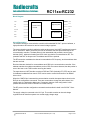
Mechanical Drawing
1.9 mm
Radiocrafts
Part nr: RCXXXX
Lot code: YYYYWW (YYYY=prod. year, WW= prod. week)
Hardware revision: A.BB
Approval marking: NN = CE, FCC or others
Top view
RCXXXX
NN
YYYYWW
A.BB
End view
3.2 mm
Side view
10.9 mm
23.6 mm
3.3 mm
0.38 mm
25.4 mm
Bottom view
12.7 mm
2.1 mm
1.4 mm
2.1 mm
8.5 mm
0.9 mm
13.6 mm
Drawings are not to scale
Mechanical Dimensions
The module size is 12.7 x 25.4 x 3.3 mm.
Carrier Tape and Reel Specification
Carrier tape and reel is in accordance with EIA Specification 481.
Tape width
44 mm
Component Hole pitch
pitch
16 mm
4 mm
Reel
diameter
13”
Units per
reel
Max 1000
Soldering Profile Recommendation
JEDEC standard IEC/JEDEC J-STD-020B (page 11 and 12), Pb-Free Assembly is
recommended.
The standard requires that the heat dissipated in the "surroundings" on the PCB is taken into
account. The peak temperature should be adjusted so that it is within the window specified in the
standard for the actual motherboard.
Aperture for paste stencil is normally areal-reduced by 20-35%, please consult your production
facility for best experience aperture reduction.
2008 Radiocrafts AS
RC11xx-RC232 Data Sheet (rev. 1.30)
Page 16 of 22
Radiocrafts
Embedded Wireless Solutions
Absolute Maximum Ratings
Parameter
Min
Supply voltage, VCC
-0.3
Voltage on any pin
-0.3
Input RF level
Storage temperature
-50
Operating temperature
-40
RC11xx-RC232
Max
3.6
VCC+0.3V
10
150
85
Unit
V
V
dBm
C
C
Caution ! ESD sensitive device.
Precaution should be used when handling
the device in order to prevent permanent
damage.
Under no circumstances the absolute maximum ratings given above should be violated. Stress
exceeding one or more of the limiting values may cause permanent damage to the device.
Electrical Specifications
T=25 C, VCC = 3.0V if nothing else stated.
Parameter
Min
Operating frequency
RC1140
433.05
RC1180
868.0
RC1190
902.0
Number of channels
RC1140
RC1180
Rc1190
Input/output impedance
Typ.
Max
Unit
434.79
870.0
928.0
MHz
Condition / Note
17
16
50
Ohm
50
Data rate
1.2
4.8
19.0
32.768
76.8
100
Frequency stability
Frequency stability aging
Transmit power
FSK deviation
Channel Filter bandwidth
kbit/s
+/-40
1
ppm
ppm/year
-20
9
dBm
5.2
58
127
540
kHz
kHz
-36
-30
dBm
Spurious emission, TX
< 1 GHz
> 1 GHz
47 – 74 MHz
87.5 – 118 MHz
174 – 230 MHz
470 – 862 MHz
Sensitivity
1.2 kbit/s
4.8 kbit/s
19.0 kbit/s
32.768 kbit/s
76.8 kbit/s
100 kbit/s
Adjacent channel rejection
-110
-108
-105
-106
-103
-101
29
dBm
Alternate channel selectivity
53
dB
Image channel rejection
28
dB
2008 Radiocrafts AS
Including 10 years of aging.
Starting after 10 years
Depends on data rate
Depends on data rate
-54
-54
-54
-54
Measured at BER 10(-3)
dB
RC11xx-RC232 Data Sheet (rev. 1.30)
Page 17 of 22
Radiocrafts
Embedded Wireless Solutions
Blocking / Interferer rejection /
desensitization
+/- 1 MHz
+/- 2 MHz
+/- 5 MHz
+/- 10 MHz
Saturation
Input IP3
Spurious emission, RX
Supply voltage
Current consumption, RX/IDLE
RC1140 TX
Current consumption, TX
-20 dBm
-10 dBm
0 dBm
5 dBm
9 dBm
RC1180/1190 TX
Current consumption, TX
-20 dBm
-10 dBm
0 dBm
5 dBm
9 dBm
Current consumption, SLEEP
Digital I/O
Input logic level, low
Input logic level, high
Output logic level, low (1µA)
Output logic level, high(-1µA)
RESET pin
Input logic level, low
Input logic level, high
UART Baud Rate tolerance
Configuration memory write
cycles
RC11xx-RC232
dB
30
35
50
60
43
49
68
72
-14
TBD
-57
3.6
2.0
dBm
dBm
dBm
V
24
mA
18
20
22
25
35
mA
16
17
22
30
37
0.3
mA
70 %
0
TBD
Wanted signal 3 dB above
sensitivity level, CW
interferer.
Minimum numbers
corresponds to class 2
receiver requirements in
EN300220.
1.0
uA
30 %
V
Apply over entire supply
voltage range
Apply over entire supply
voltage range
Of VCC
Of VCC
TBD
VCC
30 %
V
Minimum 250 ns pulse
width
70 %
+/- 2
%
1000
UART receiver and
transmitter
The guaranteed number of
write cycles using the „M‟
command is limited
Regulatory Compliance Information
The use of RF frequencies and maximum allowed RF power is limited by national regulations.
The RC1140-RC232 and RC1180-RC232 has been designed to comply with the R&TTE directive
1999/5/EC. According to R&TTE directives, it is the responsibility of Radiocrafts‟ customers (i.e.
RC11XX-RC232 end user) to check that the host product (i.e. final product) is compliant with
R&TTE essential requirements. The use of a CE marked radio module can avoid re-certification
of the final product, provided that the end user respects the recommendations given by
Radiocrafts. A Declaration of Conformity is available from Radiocrafts on request.
The RC1190-RC232 has been tested towards FCC regulations for license free operation under
part 15. However, a final approval is required by FCC for the end product.
The relevant regulations are subject to change. Radiocrafts AS do not take responsibility for the
validity and accuracy of the understanding of the regulations referred above. Radiocrafts only
guarantee that this product meets the specifications in this document. Radiocrafts is exempt from
any responsibilities related to regulatory compliance.
2008 Radiocrafts AS
RC11xx-RC232 Data Sheet (rev. 1.30)
Page 18 of 22
Radiocrafts
Embedded Wireless Solutions
RC11xx-RC232
Power Supply
Noisy external circuitry may under certain scenarios affect the transmitted signal on RC11XX-RC232
and precaution should be taken for EU R&TTE conformity. Example of circuits that can generate noise
on the RC11XX-RC232 transmitted spectrum may be DC/DC converters and some level converters
like RS232 and RS485. To increase spectrum margin it is important to add an EMI filter bead on the
VCC pin of the RC11XX-RC232 module. Alternatively the RC11XX-RC232 may be powered form a
separate voltage regulator. This will ensure that potential switching noise is filtered out from the power
supply to the RC11XX-RC232. A block diagram of a typical PC serial port interface is illustrated below.
Suggested part numbers:
Component
EMI filter bead
Manufacturer
Murata
Part number
BLM11A102S, ordering code
BLM18xx102xN1D
Programming Interface
For future firmware updates and possible custom variants it is recommended to include a 2x5 pins
programming connector to the module programming pins. The connector should be a 2.54 mm pitch
pin-row (same pitch in both directions), SMD or through-hole version, with the following connections:
GND
RC11xx Pin 20
RX11xx Pin 12, RESET
1
2 To VCC
3
4 RC11xx Pin 19
7
Reset connection
To minimize effect of noise on the Reset-line, the Reset pin on the module (pin 12) must be connected
to external circuitry via an RC-network.
2008 Radiocrafts AS
RC11xx-RC232 Data Sheet (rev. 1.30)
Page 19 of 22
Radiocrafts
Embedded Wireless Solutions
RC11xx-RC232
Appendix: ASCII Table
HEX
0
1
2
3
4
5
6
7
8
9
0A
0B
0C
0D
0E
0F
10
11
12
13
14
15
16
17
18
19
1A
1B
1C
1D
1E
1F
20
21
22
23
24
25
26
27
28
29
2A
2B
2C
DEC
0
1
2
3
4
5
6
7
8
9
10
11
12
13
14
15
16
17
18
19
20
21
22
23
24
25
26
27
28
29
30
31
32
33
34
35
36
37
38
39
40
41
42
43
44
CHR
NUL
SOH
STX
ETX
EOT
ENQ
ACK
BEL
BS
HT
LF
VT
FF
CR
SO
SI
DLE
DC1
DC2
DC3
DC4
NAK
SYN
ETB
CAN
EM
SUB
ESC
FS
GS
RS
US
SP
!
"
#
$
%
&
'
(
)
*
+
,
2D
2E
2F
30
31
32
33
34
35
36
37
38
39
3A
3B
3C
3D
45
46
47
48
49
50
51
52
53
54
55
56
57
58
59
60
61
3E
3F
HEX
40
41
42
43
44
45
46
47
48
49
4A
4B
4C
4D
4E
4F
50
51
52
53
54
55
56
57
58
59
5A
5B
5C
5D
5E
5F
60
61
62
63
64
65
66
67
68
69
6A
6B
6C
DEC
64
65
66
67
68
69
70
71
72
73
74
75
76
77
78
79
80
81
82
83
84
85
86
87
88
89
90
91
92
93
94
95
96
97
98
99
100
101
102
103
104
105
106
107
108
CHR
@
A
B
C
D
E
F
G
H
I
J
K
L
M
N
O
P
Q
R
S
T
U
V
W
X
Y
Z
[
\
]
^
_
`
a
b
c
d
e
f
g
h
i
j
k
l
.
/
0
1
2
3
4
5
6
7
8
9
:
;
<
=
6D
6E
6F
70
71
72
73
74
75
76
77
78
79
7A
7B
7C
7D
109
110
111
112
113
114
115
116
117
118
119
120
121
122
123
124
125
m
n
o
p
q
r
s
t
u
v
w
x
y
z
{
|
}
62
>
7E
126
~
63
?
7F
127
DEL
2008 Radiocrafts AS
CTRL
^@
^A
^B
^C
^D
^E
^F
^G
^H
^I
^J
^K
^L
^M
^N
^O
^P
^Q
^R
^S
^T
^U
^V
^W
^X
^Y
^Z
RC11xx-RC232 Data Sheet (rev. 1.30)
Page 20 of 22
Radiocrafts
Embedded Wireless Solutions
RC11xx-RC232
Document Revision History
Document Revision
1.0
1.1
Changes
First release
Pull-up description during sleep and additional info regarding channel
selection is added.
Updated timing table, Reset connection.
Minor correction
Mechanical drawing update, Product status change and minor corrections
1.2
1.21
1.30
Product Status and Definitions
Current
Data Sheet Identification
Status
X
Product Status
Advance Information
Planned or under
development
Preliminary
Engineering Samples
and First Production
No Identification Noted
Full Production
Obsolete
Not in Production
2008 Radiocrafts AS
Definition
This data sheet contains the design
specifications for product
development. Specifications may
change in any manner without notice.
This data sheet contains preliminary
data, and supplementary data will be
published at a later date. Radiocrafts
reserves the right to make changes at
any time without notice in order to
improve design and supply the best
possible product.
This data sheet contains final
specifications. Radiocrafts
reserves the right to make
changes at any time without notice
in order to improve design and
supply the best possible product.
This data sheet contains
specifications on a product that has
been discontinued by Radiocrafts.
The data sheet is printed for
reference information only.
RC11xx-RC232 Data Sheet (rev. 1.30)
Page 21 of 22
Radiocrafts
Embedded Wireless Solutions
RC11xx-RC232
Disclaimer
Radiocrafts AS believes the information contained herein is correct and accurate at the time of this printing. However,
Radiocrafts AS reserves the right to make changes to this product without notice. Radiocrafts AS does not assume any
responsibility for the use of the described product; neither does it convey any license under its patent rights, or the rights
of others. The latest updates are available at the Radiocrafts website or by contacting Radiocrafts directly.
As far as possible, major changes of product specifications and functionality, will be stated in product specific Errata
Notes published at the Radiocrafts website. Customers are encouraged to check regularly for the most recent updates on
products and support tools.
Trademarks
RC232™ is a trademark of Radiocrafts AS. The RC232™ Embedded RF Protocol is used in a range of products from
Radiocrafts. The protocol handles host communication, data buffering, error check, addressing and broadcasting. It
supports point-to-point, point-to-multipoint and peer-to-peer network topologies.
All other trademarks, registered trademarks and product names are the sole property of their respective owners.
Life Support Policy
This Radiocrafts product is not designed for use in life support appliances, devices, or other systems where malfunction
can reasonably be expected to result in significant personal injury to the user, or as a critical component in any life support
device or system whose failure to perform can be reasonably expected to cause the failure of the life support device or
system, or to affect its safety or effectiveness. Radiocrafts AS customers using or selling these products for use in such
applications do so at their own risk and agree to fully indemnify Radiocrafts AS for any damages resulting from any
improper use or sale.
© 2008, Radiocrafts AS. All rights reserved.
Contact Information
Web site: www.radiocrafts.com
Address:
Radiocrafts AS
Sandakerveien 64
NO-0484 OSLO
NORWAY
Tel:
+47 4000 5195
Fax:
+47 22 71 29 15
E-mail: [email protected]
[email protected]
[email protected]
2008 Radiocrafts AS
RC11xx-RC232 Data Sheet (rev. 1.30)
Page 22 of 22