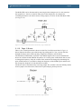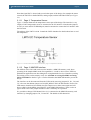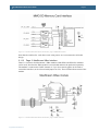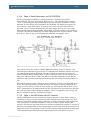
1
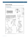
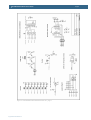
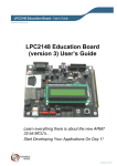
LPC2148 Education Board - User’s Guide
Copyright 2007 © Embedded Artists AB
LPC2148 Education Board
User’s Guide
Learn everything there is about the new ARM7
32-bit MCU’s…
Start Developing Your Applications On Day 1!
EA2-USG-0601 v2.1 Rev B
LPC2148 Education Board - User’s Guide
Page 2
Embedded Artists AB
Ole Römers väg 12
SE-223 70 Lund
Sweden
[email protected]
http://www.EmbeddedArtists.com
Copyright 2005-2007 © Embedded Artists AB. All rights reserved.
No part of this publication may be reproduced, transmitted, transcribed, stored in a retrieval
system, or translated into any language or computer language, in any form or by any means,
electronic, mechanical, magnetic, optical, chemical, manual or otherwise, without the prior
written permission of Embedded Artists AB.
Disclaimer
Embedded Artists AB makes no representation or warranties with respect to the contents
hereof and specifically disclaim any implied warranties or merchantability or fitness for any
particular purpose. Information in this publication is subject to change without notice and
does not represent a commitment on the part of Embedded Artists AB.
Feedback
We appreciate any feedback you may have for improvements on this document. Please send
your comments to [email protected].
Trademarks
InfraBed and ESIC are trademarks of Embedded Artists AB. All other brand and product
names mentioned herein are trademarks, services marks, registered trademarks, or registered
service marks of their respective owners and should be treated as such.
Copyright 2007 © Embedded Artists AB
LPC2148 Education Board - User’s Guide
Page 3
Table of Contents
1 Introduction
5
1.1
Contents
5
1.2
Features
5
1.3
Expansion Boards
6
1.4
ESD Precaution
7
1.5
Other Products from Embedded Artists
7
1.5.1
Design and Production Services
7
1.5.2
LPC2xxx OEM / Education / QuickStart Boards and Kits
7
2 Board Design
2.1
Board Schematics
8
2.1.1
Page 1: CPU
12
2.1.2
Page 1: UART#0 and ISP
13
2.1.3
Page 1: USB
13
2.1.4
Page 1: JTAG
14
2.1.5
Page 1: Expansion Connector
15
2.1.6
Page 2: LEDs
15
2.1.7
Page 2: Push-button
16
2.1.8
Page 2: Joystick-switch
17
2.1.9
Page 2: RGB-LED
17
2.1.10
Page 2: Buzzer
18
2.1.11
Page 2: Temperature Sensor
19
2.1.12
Page 2: MMC/SD Interface
19
2.1.13
Page 2: MaxStream XBee Interface
20
2.1.14
Page 3: Reset Generation and I2C E2PROM
21
2.1.15
Page 3: 8x8 LED Matrix with SPI Interface
21
2.1.16
Page 3: Step Motor Control
22
2.1.17
Page 3: Power Supply
23
2.1.18
Page 4: Analog Inputs
23
2.1.19
Page 4: Analog Outputs
24
2.1.20
Page 4: 2x16 Character LCD
24
2.2
2.2.1
Jumpers
Illegal Jumper Combinations
26
27
2.3
Connectors
27
2.4
Important Components
28
2.5
Mechanical Dimensions
29
3 Getting Started
30
3.1
Test program
30
3.2
Program Development
30
3.3
Program Download via ISP
30
3.4
FTDI USB Driver
31
3.4.1
Copyright 2007 © Embedded Artists AB
8
USB Driver Behavior
35
LPC2148 Education Board - User’s Guide
Page 4
4 CD-ROM and Product Registration
4.1
CD-ROM
36
4.2
Product Registration
36
5 Further Information
37
6 App.A – 10M Ethernet Expansion Board
38
6.1
Board Schematics
7 App.B – Bluetooth Expansion Board
7.1
Board Schematics
8 App.C – Graphical LCD Expansion Board
8.1
Board Schematics
9 App.D – UART & RS485 Expansion Board
9.1
Board Schematics
10
App.E – MP3 Decoder Expansion Board
10.1
11
11.1
12
12.1
Copyright 2007 © Embedded Artists AB
36
Board Schematics
App.F – ZigBee Expansion Board
Board Schematics
App.G – Prototype Expansion Board
Board Schematics
38
40
40
42
42
44
44
46
46
48
48
50
50
LPC2148 Education Board - User’s Guide
Page 5
1 Introduction
Thank you for buying Embedded Artists’ LPC2148 Education Board based on NXP’s
ARM7TDMI LPC2148 microcontroller.
This document is a User’s Guide that describes the LPC2148 Education Board hardware
design and some basic software interface principles with the hardware. There is a separate
document describing program development that also includes a lot of experiments that will
guide you through the art of embedded program development.
1.1 Contents
The box received when ordering the LPC2148 Education Board contains the following:
•
The LPC2148 Education Board.
•
A USB cable of type: mini-B-to-A, for powering and communicating with the
boards from a PC.
•
CD-ROM with additional material and programs, including complete and evaluation
versions of different development environments.
An optional JTAG interface can be used for debugging during program development. The
interface is not strictly needed but can be needed for more advanced debugging.
1.2 Features
Embedded Artists LPC2148 Education Board with NXP’s ARM7TDMI LPC2148
microcontroller lets you get up-and-running quickly. The small form factor board offers
many unique features that ease your learning curve and program development.
•
NXP ARM7TDMI LPC2148 microcontroller with 512 KByte program Flash and
32+8 KByte SRAM
•
12.0000 MHz crystal for maximum execution speed and standard serial bit rates
−
Phase-locked loop (PLL) multiplies frequency with five; 5 x 12 MHz = 60 MHz
•
32.768kHz RTC crystal
•
Onboard Peripherals
Copyright 2007 © Embedded Artists AB
−
2x16 character LCD with background light
−
Joystick switch
−
UART-to-USB bridge interface on UART #0
−
USB 2.0 device interface
−
RGB-LED, each color can be controlled via PWM signal
−
8 LEDs
−
Temperature sensor (LM75) on I2C bus
−
Pushbutton on P0.14 (interrupt input)
−
8x8 LED matrix, controlled via shift registers in the SPI bus
−
MMC/SD memory card interface
−
Step motor (bipolar driving)
LPC2148 Education Board - User’s Guide
•
−
Interface to Max Stream XBee™ module (note that XBee module is not
included)
−
Piezoelectric buzzer
−
2 Analog inputs
−
Low-pass filtering of PWM signal
−
1 Analog output
−
Reset button
Connectors
−
Mini-B USB connector to UART#0 UART-to-serial bridge)
−
Mini-B USB connector to LPC2148 device interface
−
MMC/SD memory card connector
−
JTAG
−
64 pin expansion connector, all LPC2148 I/O pins are available on connector
−
2.1 mm power supply connector
•
2 Kbit I2C E2PROM for storing non-volatile parameters
•
Onboard low-dropout voltage and reset generation.
•
•
−
Generates +3.3V (and +5V if 9-15VDC is used to power the board)
−
+3.3V available for external circuits, up to 300 mA
Power supply
−
9-15 VDC, ≥200 mA from 2.1 mm power connector
−
Can also be powered directly from any of mini-B USB connectors
Simple and automatic program download (ISP) via UART-to-serial bridge channel
−
•
Page 6
Circuit that automatically controls the bootloader from UART-to-serial bridge
channel
Dimensions: 156 x 110 mm
−
Four layer PCB (FR-4 material) for best noise immunity
1.3 Expansion Boards
The 64 pin expansion connector, with all LPC2148 I/O pins available, allows the LPC2148
Education Board to be expanded with new and exciting hardware. The experiments can be
more advanced and complex by using the expansion boards. The list below presents the first
set of available expansion boards. As seen, many of the boards are communication oriented.
•
Ethernet board (10Mbps) with SPI interface
•
Bluetooth™ board with UART interface
•
ZigBee™ board with SPI interface
•
MP3 decoder board with SPI interface
•
Graphical monochrome LCD (240x128 pixels) with parallel interface
•
Modem (UART#1) and RS485 board
Copyright 2007 © Embedded Artists AB
LPC2148 Education Board - User’s Guide
•
Page 7
Prototype board
1.4 ESD Precaution
Please note that the LPC2148 Education Board come without any case/box and all
components are exposed for finger touches – and therefore extra attention must be paid to
ESD (Electro-Static Discharge) precaution.
Make it a habit to always first touch the metal surface of one of the USB connectors or
MMC/SD connector for a few seconds with both hands before touching any other parts of
the boards. That way, you will have the same potential as the board and therefore minimize
the risk for ESD.
Note that Embedded Artists does not replace boards that have been damaged by ESD.
1.5 Other Products from Embedded Artists
Embedded Artists have a broad range of LPC2xxx based boards that are very low cost and
developed for prototyping / development as well as for OEM applications. Modifications for
OEM applications can be done easily, even for modest production volumes. Contact
Embedded Artists for further information about design and production services.
1.5.1
Design and Production Services
Embedded Artists provide design services for custom designs, either completely new or
modification to existing boards. Specific peripherals and I/O can be added easily to different
designs, for example, communication interfaces, specific analog or digital I/O, and power
supplies. Embedded Artists has a broad, and long, experience in designing industrial
electronics, in general, and with NXP’s LPC2xxx microcontroller family, in specific. Our
competence also includes wireless and wired communication for embedded systems. For
example IEEE802.11b/g (WLAN), Bluetooth™, ZigBee™, ISM RF, Ethernet, CAN, RS485,
and Fieldbuses.
1.5.2
LPC2xxx OEM / Education / QuickStart Boards and Kits
Visit Embedded Artists’ home page, www.EmbeddedArtists.com, for information about
other QuickStart boards / kits or contact your local distributor.
Copyright 2007 © Embedded Artists AB
LPC2148 Education Board - User’s Guide
Page 8
2 Board Design
This chapter contains detailed information about the electrical and mechanical design of the
LPC2148 Education Board.
2.1 Board Schematics
Figure 1 - LPC2148 Education Board Schematic v2.1, page 1
Copyright 2007 © Embedded Artists AB
LPC2148 Education Board - User’s Guide
Figure 2 - LPC2148 Education Board Schematic v2.1, page 2
Copyright 2007 © Embedded Artists AB
Page 9
LPC2148 Education Board - User’s Guide
Figure 3 - LPC2148 Education Board Schematic v2.1, page 3
Copyright 2007 © Embedded Artists AB
Page 10
LPC2148 Education Board - User’s Guide
Page 11
Figure 4 - LPC2148 Education Board Schematic v2.1, page 4
The following subsections describe in more detail each part of the design. Each schematic
page is described in turn.
Copyright 2007 © Embedded Artists AB
LPC2148 Education Board - User’s Guide
2.1.1
Page 12
Page 1: CPU
The core part of the design is the NXP LPC2148 microcontroller. It’s an ARM7TDMI-S
CPU core with a lot of different peripheral units and on-chip memory (512 kByte FLASH
and 32-8 kByte SRAM). There is no external memory bus interface. Figure 5 below
illustrates the CPU section of the design.
Figure 5 - LPC2148 Education Board Schematic, page 1: CPU
The microcontroller crystal frequency is 12.0000 MHz. This frequency has been selected in
order to allow maximum execution speed (5 x 12 MHz = 60 MHz, which is the maximum
frequency). The on-chip UART peripheral includes a fractional baud rate generator that
allow standard baud rates to be generated from the 60 MHz base clock. The USB clock (48
MHz) is also generated from the 60 MHz clock without any problems.
There is also a 32.768 kHz crystal clock for the on-chip real-time clock peripheral unit or
RTC for short. The microcontroller can be placed in a very low power mode while the RTC
operates and keeps track of time. Power for the RTC (during these low power modes) comes
from the VBAT input pin. Power is sourced either from the +3.3V power supply or the
external VBAT_IN signal (available on the expansion connector), depending on which one
have highest voltage.
The LPC2148 also contains an Analog-to-Digital Converter or ADC for short, as well as a
Digital-to-Analog Converter (DAC). These two peripheral units need a reference voltage,
which is supplied from the VREF input pin.
Copyright 2007 © Embedded Artists AB
LPC2148 Education Board - User’s Guide
Page 13
Jumper J3 selects two different sources for VREF. The CPU power supply (+3.3V) is used
and divided by 3/2. The power supply is low-pass filtered for noise immunity. The precision
of the power supply is 1%. Alternatively an external precision voltage is used, the VREF_IN
pin on the expansion connector.
2.1.2
Page 1: UART#0 and ISP
UART#0 on the LPC2148 is connected to a USB-to-serial bridge chip (FT232RL from
FTDI). The serial interface is not a full interface, only the receive and transmit signals are
connected to UART#0. There are two UART channels on the LPC2148 and only channel #1
has all control signals needed for a full modem implementation. Channel #0 only has receive
and transmit signals. Channel #1 is free and used by some of the expansion boards.
There are two LEDs connected to the USB-to-serial bridge chip. These indicate Rx and Tx
activity and can be a good help when determining if a connection with the board is working
properly.
Even though the CPU clock crystal is 12.000 MHz, any standard baud rate can be generated
since both UART channels have a fractional baud rate generator. ‘Fractional’ means that the
clock frequency does not have to be divided by an even integer value. It can also be divided
by a fractional value, which means that a lot more baud rates can be achieved from basically
any clock crystal frequency. There is even an autobauding capability, meaning that basically
any baud rate can be detected. Read more about this functionality in the LPC2148 datasheet.
The interface can be disconnected by removing the jumpers on J6, in case an external UART
interface is to be designed (for example on a prototype board).
Finally there is a special circuit to automate the ISP feature (In-System Programming). With
the help of two control signals (RTS and DTR), the processor can be placed in the bootloader
mode. The bootloader uses UART#0 for downloading new program images into the
processor (either into FLASH or into RAM). DTR controls the processor reset and RTS can
pull signal P0.14 low. If the processor samples P0.14 low after reset the bootloader is
entered, else the application code is executed. The automatic ISP functionality can be
disabled by removing the two bottom jumpers on J6. Note that some terminal programs
(notably Windows™ Hyperterminal) control the RTS/DTR signals in an unfavorable way so
that the board always enters bootloader mode or is always in reset more. In these cases, the
jumpers must be removed or a serial cable with only receive and transmit signals must be
used.
Figure 6 below illustrates the USB-to-serial interface and ISP part of the design.
Figure 6 - LPC2148 Education Board Schematic, page 1: USB-to-serial and ISP
2.1.3
Page 1: USB
The LPC2148 also contains a USB 2.0 device interface as one of its peripheral units. Figure
7 below illustrate the USB part of the design. Low-pass filtering is added for noise
immunity. The USB interface supports the Soft Connect functionality and voltage sense (see
Copyright 2007 © Embedded Artists AB
LPC2148 Education Board - User’s Guide
Page 14
LPC2148 User’s Manual for more information about these functions). The Soft Connect
feature is controlled by IO-pin P0.31 and is activated by placing a 1.5 kohm resistor between
the D+ signal and +3.3V. A green LED also is on when the resistor is resent. The voltage
sense feature is handled by IO-pin P0.23, which is connected to VCC of the USB interface.
Figure 7 - LPC2148 Education Board Schematic, page 1: USB
2.1.4
Page 1: JTAG
The JTAG interface is a standard 20-pin (2x10) connector with shoulders – ‘standard’, at
least in the ARM world. The JTAG interface shares 6 general IO-pins (GPIOs) and is
enabled by shorting jumper J5, i.e., pulling P1.26 low during reset. When the JTAG interface
is enabled, the 6 IO-pins cannot be used for other purposes than the JTAG interface. Figure
8 below illustrates the JTAG part of the schematics.
Figure 8 - LPC2148 Education Board Schematic, page 1: JTAG
Copyright 2007 © Embedded Artists AB
LPC2148 Education Board - User’s Guide
Page 15
To use the JTAG interface of the LPC2148 Education Board a special JTAG interface pod
must be used. This pod must be integrated with a debugger in order to do anything useful
with it. There exist many different manufacturers of JTAG interface pods.
2.1.5
Page 1: Expansion Connector
The LPC2148 Education Board is not just a monolithic design. Via the expansion connector,
it’s possible to expand the design. All LPC2148 pins are available on the expansion
connector, which is a standard 2x32 pin list with 100 mil pin spacing. Figure 9 below
illustrates the expansion connector part of the design.
Figure 9 - LPC2148 Education Board Schematic, page 1: Expansion Connector
The power voltages, +5V and +3.3V, are available on the expansion connector. Note that the
current consumption of external circuitry on the expansion boards must be low. The onboard +3.3V voltage regulator can only supply up to 300 mA to external circuits. Note also
that an external power supply (+9-15 VDC) must be able to deliver all needed current. In the
case that the USB port is used to power the board, the total current consumption must be less
than 500 mA. Else the USB host in the other end will shut down current delivery completely.
2.1.6
Page 2: LEDs
The port pins of the LPC2148 microcontrollers have a 4 mA driving capacity, enough to
directly drive LEDs. Figure 10 below illustrates the 8 LEDs in the design. The LEDs are
connected to pin P0.8 – P0.15 and are red. The 1kohm resistors limit the current to about 2
mA. A low output pin drives current through the LEDs and they will light. Each LED can be
individually enabled or disabled via jumpers:
•
J8 – P0.8
•
J10 – P0.9
Copyright 2007 © Embedded Artists AB
LPC2148 Education Board - User’s Guide
•
J13 – P0.10
•
J15 – P0.11
•
J18 – P0.12
•
J19 – P0.13
•
J20 – P0.14
•
J21 – P0.15
Page 16
Figure 10 - LPC2148 Education Board Schematic, page 2: LEDs
2.1.7
Page 2: Push-button
The signal P0.14 can be configured as an interrupt input pin on the processor. A push-button
is connected to this signal so it’s possible to pull the signal low. There is a pull-up resistor
(10 kohm) on the signal, which is also needed for the ISP feature. The signal P0.14 must be
sampled high after reset in order to start normal program execution; else the internal
bootloader will be activated. Figure 11 below illustrates the push-button part of the design.
Copyright 2007 © Embedded Artists AB
LPC2148 Education Board - User’s Guide
Page 17
Figure 11 - LPC2148 Education Board Schematic, page 2: Push-button
2.1.8
Page 2: Joystick-switch
There is a joystick-switch on the board and Figure 12 below illustrates this part of the
design. The switch has five internal switches, one for the four directions and one center,
push-down switch. All of the input pins (P0.16 – P0.20) can be programmed as interrupt
inputs, either directly as an EINTx-pin or via a CAPture-pin, which in turn can generate an
interrupt.
Figure 12 - LPC2148 Education Board Schematic, page 2: Joystick-switch
2.1.9
Page 2: RGB-LED
There is a full color RGB-LED that can be controlled by PWM (Pulse Width Modulated)
signals. The intensity of each LED can easily be controlled by adjusting the pulse width of
the signals. The list below explains the signal connections.
•
Red LED, controlled by signal P0.7 – PWM2
•
Blue LED, controlled by signal P0.8 – PWM4
•
Green LED, controlled by signal P0.9 – PWM6
The PWM signals are available as alternative signals on the pins and are generated from the
PWM peripheral unit. Figure 13 below illustrates the RGB-LED part of the design.
Note that the LEDs are driven from the +5V power supply. This is because the forward
voltage drop of the blue LED is typically around 3.5V, which is more than the 3.3V power
supply for the LCP2148.
Copyright 2007 © Embedded Artists AB
LPC2148 Education Board - User’s Guide
Page 18
The RGB-LED can be disconnected by removing the three jumpers on J16. Also note that
the signals P0.8 – P0.10 are used for other parts of the design also, for example for
controlling the buzzer, the motor control, analog output, as well as for the individual LEDs
(see Figure 10).
Figure 13 - LPC2148 Education Board Schematic, page 2: RGB-LED
2.1.10
Page 2: Buzzer
There is also a small piezoelectric buzzer on the LPC2148 Education Board. Figure 14
below illustrate the buzzer part of the design. By pulling pin P0.7 low, current will flow
through the buzzer and a relatively sharp, single-tone frequency will be heard.
The alternative PWM feature of pin P0.7 (the PWM2 signal) can be used to modulate the
buzzer to oscillate around different frequencies. It’s not the pulse width feature that is used
to change the frequency. Only the volume of the sound will be changed by alternating the
pulse width. Instead, it’s possible to change the frequency of the PWM signal, and this will
also change the frequency of with the buzzer oscillate.
The buzzer can be disconnected by removing jumper J22, and this is also the default position
for this jumper since the buzzer sound can be quite annoying if always left on.
Figure 14 - LPC2148 Education Board Schematic, page 2: Buzzer
Copyright 2007 © Embedded Artists AB
LPC2148 Education Board - User’s Guide
Page 19
Note that signal P0.7 is shared with several other parts of the design, for example the motor
control, the red LED in the RGB-LED, analog output, and the individual LEDs (see Figure
10).
2.1.11
Page 2: Temperature Sensor
Figure 15 below illustrates the temperature sensor part of the design. The interface is very
simple; a LM75 temperature sensor is connected to the I2C interface. Note that the jumpers
on J25 (see reset and I2C-E2PROM part) must be mounted to connect the I2C interface with
the LPC2148.
The address of the LM75 is 0x90. Consult the LM75 datasheet for details about how to read
the temperature.
Figure 15 - LPC2148 Education Board Schematic, page 2: Temperature Sensor
2.1.12
Page 2: MMC/SD Interface
The SPI bus of the LPC2148 can be used to interface a MMC/SD memory card, when
operating in the simpler MMC mode. Pin/signal P0.11 is used as device select. NXP has
published an application note describing how to implement the low-level interface (reading
and writing sectors on the memory card). See AN10406: Accessing SD/MMC card using
SPI on LPC2000 for details. Figure 16 below illustrates the MMC/SD interface part of the
design.
The interface can be disconnected from the LCP2148 by removing jumpers J9, J11, J14, and
J17. Also note that bottom jumper on J24 (SPI_MISO to P0.5 the SPI interface for the 8x8
LED matrix) should not be installed since this output is not a three-state output and will
hence collide with the MISO signal (DOUT on the MMC/SD interface). There is also no
typical need to have this jumper installed so this is normally not a problem.
It’s possible to change if SPI channel #0 or #1 is connected to the MMC/SD memory card
interface, by changing jumpers J11, J14 and J17. The default is SPI channel #0.
Copyright 2007 © Embedded Artists AB
LPC2148 Education Board - User’s Guide
Page 20
Figure 16 - LPC2148 Education Board Schematic, page 2: MMC/SD Interface
Note that the switches for ‘card detect’ and ‘write protect’ are not connected at all in this
design.
2.1.13
Page 2: MaxStream XBee Interface
There is a connector for MaxStream’s XBee modules. Both XBee and XBee Pro modules
can be used. Note that the XBee module is not included and must be purchased separately.
The module is connected to UART channel #1. Up to four control signals can be used to
control the interface (can be selected with jumpers on J23). Three LEDs indicate status of the
module.
Figure 17 - LPC2148 Education Board Schematic, page 2: XBee interface
Copyright 2007 © Embedded Artists AB
LPC2148 Education Board - User’s Guide
2.1.14
Page 21
Page 3: Reset Generation and I2C E2PROM
The rest generation is handled by a mixed-signal chip, CAT1025 from Catalyst
Semiconductor. The reset signal will be held active (i.e., low) until the supply voltages,
+3.3V, is within margins. The reset duration is typically 200 mS (consult the CAT1025
datasheet for exact details, also included on the CD-ROM). The output reset signal is an
open-collector / open-drain output. An external reset source can also control the reset
generator. Figure 18 below illustrates this part of the design. There is also a reset pushbutton (SW1) and both the signals RES_IN and RES_OUT are available on the expansion
connector. Note that an external driver of these signals should be an open-collector / opendrain driver. There is also a red LED that lights when the reset signal is active.
Figure 18 - LPC2148 Education Board Schematic, page 3: Reset Generation and I2C E2PROM
The CAT1025 chip also contains a 2kbit E2PROM accessible via the I2C interface. The
LPC2148 microcontroller has two on-chip I2C communication channels. Channel #0 is used
for communicating with the E2PROM. The other channel can optionally be used on an
expansion board. More peripheral units are easily connected to the two-wire I2C bus, just as
long as the addresses do not collide. The address of the 2kbit E2PROM is 0xA0. The I2C
interface to the CAT1025 can be disconnected from the LPC2148 by removing jumpers on
J25.
Note that the pull-up resistors (which are always needed on I2C busses) are included on the
board. These pull-up resistors are 3000 ohm each. If using the second I2C channel do not
forget to connect pull-up resistors to these signals also. Note that this must be done even if
the I2C functionality is not used/enabled. Pins P0.11 and P0.14 are open-drain I/Os and must
have pull-up resistors when configured as outputs. This is unfortunately easy to forget, but
they are included on the LPC2148 Education Board.
2.1.15
Page 3: 8x8 LED Matrix with SPI Interface
The 8x8 LED matrix is the most advanced circuit on the board, at least when it comes to
controlling it. Figure 19 below illustrate the 8x8 LED matrix part of the design. Two shift
registers (serial-input, parallel-output), 74HC595, are used to control the eight columns and
rows respectively. 16 bits must be shifted (= 2 bytes) in order to update the two shift
registers. The first byte sent controls the rows and the second byte the columns. A zero bit in
the first byte will light LEDs for the corresponding row and a zero bit in the second byte will
light LEDs for the corresponding column. In order to display arbitrary patterns on the display
a time-multiplexing mechanism must be implemented where each column (or row) is
Copyright 2007 © Embedded Artists AB
LPC2148 Education Board - User’s Guide
Page 22
updated one at a time in a circular pattern. The update frequency must be higher than 100 Hz
in order not to see flickering on the LEDs.
The LPC2148 microcontroller has two on-chip SPI serial communication channels. The shift
registers are accessed via the SPI bus, channel #0, and signal P0.15 is used as device select
pin. SPI mode 0 can be used to shift data into the shift registers. SPI channel #0 is also
shared with the MMC/SD interface.
Figure 19 - LPC2148 Education Board Schematic, page 3: 8x8 LED Matrix with SPI Interface
The 8x8 LED matrix circuit can be disconnected from SPI channel #0 by removing the
jumpers on J24. Normally, the bottom jumper on J24 (SPI_MISO on P0.5) should not be
inserted since the output from U11 is not three-states when the shift registers are not enabled
by device select signal P0.15. If inserted, the output from U11 will collide with the data
output (DOUT) from the MMC/SD interface. The only reason to have this jumper inserted
would be to read back the last two bytes shifted into the shift registers (and there is no
typical reason to do this).
2.1.16
Page 3: Step Motor Control
The board includes a small bipolar step motor with a propeller mounted so movements can
easily be observed. Signals P0.12 and P0.21 are used to control the movement of the step
motor. Bipolar control of a step motor means that the current must flow in one (of two
possible) directions through the windings. Two output buffers (4428-type drivers) make sure
the motor windings are driven correctly. To rotate the axis one of the following two output
patterns must be used.
Forward
Reverse
P0.12
P0.21
Figure 20 below illustrates the step motor control part of the design.
Copyright 2007 © Embedded Artists AB
LPC2148 Education Board - User’s Guide
Page 23
Figure 20 - LPC2148 Education Board Schematic, page 3: Step Motor Control
2.1.17
Page 3: Power Supply
The power supply uses conventional low-dropout voltage regulators, the Sipex SP1117. The
LPC2148 need only a single +3.3V voltage and has an internal 1.8V regulator for powering
the core. Some other processors in the LPC2xxx series require both a +3.3V and a +1.8V
voltage. For a full specification of the SP1117 voltage regulator see the datasheet from Sipex
(also included on the CD-ROM).
Figure 21 below illustrates the voltage regulator part of the design. As seen, power can come
from either an external power adapter via a standard 2.1 mm power connector or from the
two USB connectors (see schematic page #1 for details). Diode D10 and the diodes on the
USB interfaces feeds the VIN power signal. The diodes are needed in order for any power
supply input to feed the power and for blocking the USB interfaces from being reverse-fed.
Normally, power is taken from the USB connector, but in some cases the 2.1 mm connector
can be used, for example when the power need for expansion boards is high and the USB
cannot supply the needed current (≥500mA).
Figure 21 - LPC2148 Education Board Schematic, page 3: Power Supply
There are three pads to ease measurements of the incoming (+5V) voltage and the generated
(+3.3V) voltage, see PAD3 – PAD5. A green LED indicates the presence of +3.3V voltage.
2.1.18
Page 4: Analog Inputs
The LPC2148 has 14 analog inputs connected to two different 10-bit ADC (Analog-toDigital Converter). The conversion time is as short as 2.44 us and the input pins VREF and
VSSA are used as conversion reference. Figure 23 below illustrates the analog input part of
the design. As seen, two trim-potentiometers are used to generate a variable voltage to
Copyright 2007 © Embedded Artists AB
LPC2148 Education Board - User’s Guide
Page 24
analog input #1 (P0.28) and #2 (P0.29). Note that the analog inputs are counted from analog
input #0, but this input is not used in this design.
The signals P0.28 and P0.29 can be used as general purpose pins if the analog inputs are not
used and in this case the analog voltages can easily be removed by removing the two
jumpers on J28.
Figure 22 - LPC2148 Education Board Schematic, page 4: Analog Inputs
2.1.19
Page 4: Analog Outputs
The LPC2148 has one analog output, available as an alternative function on pin P0.25.
Figure 23 below illustrate the analog output part of the design. Via jumper J29 it is possible
to connect the analog input to analog input #3 (P0.30). There are also special pads to make it
easier to measure the analog voltage (PAD6 and PAD9).
It’s also possible to generate an analog output voltage by filtering a PWM signal. Also in this
case, the alternative PWM2 signal on P0.7 is used and low-pass filtered. It’s possible to
measure the result with analog input #3. An oscilloscope can with advantage be used to
measure the PWM signal before and after the low-pass filtering. The cut-off frequency is 1 /
(2πRC) = about 2 Hz, which means that any PWM signal with a reasonable high frequency
will be adequately low-pass filtered. It’s also possible to measure if the remaining ripple is
what can be expected from a simple 1-pole low-pass filter like this.
Figure 23 - LPC2148 Education Board Schematic, page 4: Analog Outputs
2.1.20 Page 4: 2x16 Character LCD
The final part of the LPC2148 Education Board is the 2x16 character LCD. The interface to
the LCD is a simulated memory bus. 11 pins are needed to create an 8-bit interface; 8 data
bits (D0-D7), 1 address bit (RS), 1 read/write bit (R/W), and one control signal (E). It’s also
possible to control the backlight via signal P0.30. The LCD controller is a standard
KS0070B or equivalent, which is a very well-known interface for smaller character based
LCDs.
Copyright 2007 © Embedded Artists AB
LPC2148 Education Board - User’s Guide
Page 25
Figure 24 below illustrate the LCD part of the design and which pins are used for the
interface. All pins can be disconnected from the interface if needed, via jumpers J31 – J42.
The LCD is powered from the +3.3V power supply. The display contrast adjustment (via
R86) is not mounted since the currently used LCD does not need adjusted.
Figure 24 - LPC2148 Education Board Schematic, page 4: 2x16 Character LCD
There are two options to reduce the number of pins used for the interface.
•
Do not use the R/W pin and save one pin (P0.22). Normally, there is only a need to
write to the display controller. In this case, the R/W signal can be tied low
permanently (R84) and jumper J40 is removed.
•
Use the 4-bit interface instead of the 8-bit interface. The LCD controller can operate
from a 4-bit interface. In this case, data bus pins D4 – D7 are just used. In this case 4
pins will be free (P1.16 – P1.19) for other use. If combined with the option above,
five pins will be freed.
Copyright 2007 © Embedded Artists AB
LPC2148 Education Board - User’s Guide
Page 26
2.2 Jumpers
The LPC2148 Education Board is full of jumpers in order to be able to connect/disconnect
all different parts of the external circuits. Figure 25 below illustrates all jumpers and
explains to what part of the design they belong.
XBee Interface
J23, in order from
top to bottom:
P0.15
P0.13
P0.11
P0.10
P0.9
P0.9
UART#0 and automatic ISP
J6, in order from left
to right:
ISP-RESET
ISP-P0.14
TxD
RxD
I2C E2PROM
J25, in order from
top to bottom:
SCL, P0.2
SDA, P0.3
Enable JTAG
J5
RGB-LED
J16, in order from
left to right:
P0.7 - Red
P0.8 - Blue
P0.9 - Green
MMC/SD Interface
In order from top
to bottom:
J9 (Select, P0.11)
J17 (MISO, P0.5 left, P0.18 right)
J11 (MOSI, P0.6 left, P0.19 right)
J14 (SCK, P0.4, left, P0.17 right )
8x8 LED Matrix
J24, in order from
top to bottom:
P0.5 - MISO
P0.15 - Select
P0.4 - SCK
P0.6 - MOSI
Analog-PWM
J29 (P0.7)
Buzzer
J22 (P0.7)
Motor Control
J26, in order from
top to bottom:
P0.21 - Phase1
P0.12 - Phase2
Analog Inputs
J28, in order from
left to right:
P0.28, AIN1
P0.29, AIN2
Figure 25 - LPC2148 Education Board Jumpers
Copyright 2007 © Embedded Artists AB
VREF
J3
Left pos: from 3.3V
Right pos: VREF IN
Analog Output
J30 (P0.30, AIN3)
Left pos: PWM-LP
Right pos: AOUT (P0.25)
2x16 Character LCD
In order from left
to right:
J39 (RS, P1.24)
J40 (R/W, P0.22)
J41 (E, P1.25)
J31 (D0, P1.16)
J32 (D1, P1.17)
J33 (D2, P1.18)
J34 (D3, P1.19)
J35 (D4, P1.20)
J36 (D5, P1.21)
J37 (D6, P1.22)
J38 (D7, P1.23)
J42 (backlight, P0.30)
LEDs
In order from left
to right:
J21 (P0.15)
J20 (P0.14)
J19 (P0.13)
J18 (P0.12)
J15 (P0.11)
J13 (P0.10)
J10 (P0.9)
J8 (P0.8)
LPC2148 Education Board - User’s Guide
2.2.1
Page 27
Illegal Jumper Combinations
Note that some jumpers are mutual exclusive and should not be inserted simultaneously.
•
MISO signal (P0.5) on SPI channel #0. Do not have bottom jumper on J24 inserted
simultaneously as the MMC/SD interface is used. See explanation in section 2.1.12
•
P0.7 is a commonly used signal that is used for the buzzer, the red LED in the RGBLED, and individual LED.
•
Many of the signals for the individual LEDs (P0.8 – P0.15) are also used for other
parts of the design. It does not damage the electronics if the LEDs are connected,
and in some cases it might even be useful to have LED indicators for some signals.
2.3 Connectors
Figure 26 below illustrate the position of all external connectors on the LPC2148 Education
Board.
XBee module
connector
U6
USB
J7
USB
J1
Input power
J27
JTAG
J4
MMC/SD
J12
Expansion
connector
J2
Figure 26 - LPC2148 Education Board External Connectors
Copyright 2007 © Embedded Artists AB
LPC2148 Education Board - User’s Guide
Page 28
2.4 Important Components
Figure 27 below illustrates the position on the board for some important components in the
design.
USB RX/Tx
LEDs
USB connect
LED
Voltage measurement
pads
XBee LEDs
Power
LED
(+3.3V)
Reset
LED
Reset
push-button
Voltage measurements
pads for analog output
Figure 27 - LPC2148 Education Board Important Components
Copyright 2007 © Embedded Artists AB
LPC2148 Education Board - User’s Guide
Page 29
2.5 Mechanical Dimensions
Figure 28 below contains a drawing of the board that includes mechanical measures. As
seen, the board is 156 x 110 mm large with mounting holes 144 x 98 mm apart.
98 mm
5.5 mm
144 mm
156 mm
Figure 28 - LPC2148 Education Board Mechanical Dimensions
Copyright 2007 © Embedded Artists AB
6 mm
110 mm
LPC2148 Education Board - User’s Guide
Page 30
3 Getting Started
3.1 Test program
The LPC2148 Education Board comes preloaded with a test program. This program can be
used to verify that the board operates correctly.
•
Download the test program (by using the hex-file for the test program)
•
Insert all jumpers according to default positions
•
Push the reset button
•
Watch the running-one on the individual LEDs.
•
Also watch the printed information on the terminal (se below)
•
After that a test loop is entered:
o
Printed message on the LCD and flashing of backlight
o
Scrolled message on 8x8 LED matrix
o
PC-mouse emulation over USB and joystick-switch
o
Dimming of RGB-LEDs
o
Running the step motor forward and backward
A terminal program should be attached to the USB-to-serial mini-B USB connector. The test
program will output test information regarding the I2C and E2PROM test, MMC/SD test, as
well as the RTC crystal test. Also, the UART/USB channel can be tested by typing
characters in the terminal program. The settings for the terminal program are: 38.4 kbps, 8
data bits, no parity bits, and one stop bit (i.e., 8N1).
3.2 Program Development
Consult the QuickStart Program Development User’s Manual for more information about
the QuickStart Build Environment from Embedded Artists, and program development for the
ARM7 in general.
3.3 Program Download via ISP
UART#0 can be used to download program code into the internal FLASH of the LPC2148.
The ISP (In-System Programming) feature of the LPC2148 is then used. ISP is enabled after
reset by pulling pin P0.14 low. In order to enable automated ISP invocation, the LPC2148
Education Board allows control of both the reset signal and P0.14, via the USB-to-serial
bridge (FT232RL from FTDI). Reset is controlled by the DTR serial signal and P0.14 via
RTS. NXP has release a download program (no longer supported) and there is also the open
source LPC21ISP program. FlashMagic from ES Academy is however the recommended
ISP download program to use. The program can be downloaded from:
http://www.flashmagictool.com/
Figure 29 below illustrates the jumper settings when enabling the automatic ISP
functionality.
Copyright 2007 © Embedded Artists AB
LPC2148 Education Board - User’s Guide
Page 31
UART#0 and automatic ISP
J6, in order from left
to right:
ISP-RESET
ISP-P0.14
TxD
RxD
Figure 29 – ISP Jumpers, enable automatic ISP
Some terminal programs can control the DTR/RTS signals when connected to the board so
that the board is constantly in reset or always enabling ISP mode. In that case, the automatic
ISP functionality must be disabled. Figure 30 below illustrates the jumper settings then
disabling the automatic ISP.
Disabling automatic ISP
Only TxD and RxD of
UART#0 connected.
RESET and P0.14 signals
cannot be controlled over
the USB-to-Serial bridge.
Figure 30 – ISP Jumpers, disable automatic ISP
Note that the USB-to-Serial bridge chip must have its driver installed on the PC FlashMagic
and the terminal program is running from. Section 3.4 below describes the installation
procedure.
3.4 FTDI USB Driver
A USB driver must be installed on your PC computer in order for the USB-to-UART chip
(FT232R) to function. Make sure to download the latest version of the driver, which can be
found at the following URL: http://www.ftdichip.com/Drivers/VCP.htm (search for a
FT232R driver for your operating system). Latest version of the driver (at the time of writing
this document) is 2.00.00.
When the LPC2148 Education Board is connected to the PC (via an USB cable) the PC will
ask for a driver. Unpack/unzip the downloaded driver file and browse to the position of the
driver files. After successful driver installation, a COM port will be created. Before
Copyright 2007 © Embedded Artists AB
LPC2148 Education Board - User’s Guide
Page 32
communication with the Board can take place the UART settings must be correctly set. The
following description is valid for Windows™ XP, but other operating systems have similar
dialog windows. See the USB driver documentation for details, if needed.
To change UART settings, first open the System Properties dialog, as illustrated in the figure
below.
Device
Manager
Figure 31 – System Settings Dialog
Then select the Device Manager and then open the Ports list, as illustrated in Figure 32
below.
Copyright 2007 © Embedded Artists AB
LPC2148 Education Board - User’s Guide
Page 33
Ports
Figure 32 – Device Manager Dialog
The new COM port (USB Serial Port) will be listed under the Ports list. Right-click on the
new USB Serial Port and select Properties, as illustrated in Figure 33 below.
USB Serial Port
Properties
Figure 33 – Device Manager Port Dialog
Set 38400 bits per second, 8 data bits, none parity, 1 stop bit, and none flow control, as
illustrated in Figure 34 below. Then select Advanced settings.
Copyright 2007 © Embedded Artists AB
LPC2148 Education Board - User’s Guide
Page 34
UART settings
Advanced
settings
Figure 34 – USB Serial Port Properties Dialog
Set the desired COM port number under the Advanced settings dialog. NXP’s FLASH Utility
program (for ISP program download) needs, for example, a COM port number between 1
and 5. Very often the COM port number selected but the USB Serial Port is higher than this,
so this needs to be changed manually.
It is common that all COM ports with low numbers are listed as occupied, but test to change
to a low number anyways. Very often it’s no problem at all to do this.
COM Port
Number Setting
Figure 35 – Advanced USB Serial Port Properties Dialog
Finally it’s time to test if you have successfully installed and configured the USB Serial Port.
Start a terminal program. Connect to the correct COM port, with 38400 bits per second, 8N1,
no flow control. Remember to not have the USB-ISP jumpers inserted.
Copyright 2007 © Embedded Artists AB
LPC2148 Education Board - User’s Guide
3.4.1
Page 35
USB Driver Behavior
Sometimes the USB COM port does not enumerate properly when the board in connected to
the PC. This is a known “feature” of the USB driver. If you experience this problem, just
unplug the board shortly and then plug in again. A new COM port that can be accessed
properly should be created the second time.
This problem may occur after every time you start (i.e., power cycle) your PC.
If the ISP jumpers are inserted, pressing the reset button is often required in order to startup
the board (it can be placed in bootloader mode during startup due to RTS/DTR signal
handling by the USB driver during startup).
Copyright 2007 © Embedded Artists AB
LPC2148 Education Board - User’s Guide
Page 36
4 CD-ROM and Product Registration
The accompanying CD-ROM contains a lot of information and programs that will easy your
program development! Note that there may be newer versions of different documents and
programs available than the ones on the CD-ROM. See Section 4.2 for information about the
product registration process, which allows you to always have access to the latest versions.
4.1 CD-ROM
The following is included on the CD-ROM:
•
The preloaded test program as a HEX-file.
•
The two different ISP download programs.
•
Datasheets of all circuits on the LPC2148 Education Board.
•
QuickStart Build Environment from Embedded Artists, which contains a complete
setup of a build environment for GCC.
•
A complete development environment: Rowley Associates CrossWorks for ARM,
30-day evaluation version.
•
A complete development environment: IAR Embedded Workbench for ARM,
Kickstart Edition with 32 Kbyte program size limit.
•
Another complete development environment: GCC, GNUARM distribution,
including compiler, linker, make, and debugger.
•
The program Programmers Notepad, which is a very good program development
editor and project manager.
•
The Eclipse development environment including the CDT (C/C++ Development
Tools) project.
4.2 Product Registration
By registering as a customer of Embedded Artists you will get access to more valuable
material that will get you up-and-running instantly:
•
Access to a Real-Time Operating System (RTOS), in the form of a library that can
be used for non-commercial applications.
•
Access to a number of sample applications that demonstrated different (peripheral)
functions in the LPC2148 processor.
•
Access to the latest versions of all information and programs on the CD-ROM.
Registering is easy and done quickly.
1) Go to http://www.EmbeddedArtists.com, select Support and then Register.
2) Type in the products serial number (can be found on the LPC2148 Education Board
or on the package carrying the board) along with your personal information.
Copyright 2007 © Embedded Artists AB
LPC2148 Education Board - User’s Guide
Page 37
5 Further Information
The LPC2148 microcontroller is a complex circuit and there exist a number of other
documents with a lot more information. The following documents are recommended as a
complement to this document.
[1] NXP LPC2148 Datasheet
http://www.nxp.com/acrobat/datasheets/LPC2141_42_44_46_48_2.pdf
[2] NXP LPC2148 User’s Manual
http://www.nxp.com/acrobat/usermanuals/UM10139_1.pdf
[3] NXP LPC2148 Errata Sheet
http://www.nxp.com/acrobat/erratasheets/2148.pdf
[4] ARM7TDMI Technical Reference Manual. Document identity: DDI0029G
http://www.arm.com/pdfs/DDI0029G_7TDMI_R3_trm.pdf
[5] ARM Architecture Reference Manual. Document identity: DDI0100E
Book, Second Edition, edited by David Seal, Addison-Wesley: ISBN 0-201-73719-1
Also available in PDF form on the ARM Technical Publications CD
[6] ARM System Developer’s Guide – Designing and Optimizing System Software, by
A.N. Sloss, D Symes, C. Wright. Elsevier: ISBN 1-55860-874-5
[7] Embedded System Design on a Shoestring, by Lewin Edwards.
Newnes: ISBN 0750676094.
[8] GNU Manuals
http://www.gnu.org/manual/
[9] GNU ARM tool chain for Cygwin
http://www.gnuarm.com
[10] An Introduction to the GNU Compiler and Linker, by Bill Gatliff
http://www.billgatliff.com
[11] LPC2000 Yahoo Group. A discussion forum dedicated entirely to the NXP LPC2xxx
series of microcontrollers.
http://groups.yahoo.com/group/lpc2000/
[12] The Insider’s Guide to the NXP ARM7-Based Microcontrollers, by Trevor Martin.
http://www.hitex.co.uk/arm/lpc2000book/index.html
Especially note document [3]. There exist a number of bugs in the processor that is important
to be aware of.
Note that there can be newer versions of the documents than the ones linked to here. Always
check for the latest information / version.
Datasheets for all circuits on the LPC2148 Education Board are included on the
accompanying CD-ROM.
Copyright 2007 © Embedded Artists AB
LPC2148 Education Board - User’s Guide
Page 38
6 App.A – 10M Ethernet Expansion Board
This chapter contains detailed information about the electrical design of the board.
6.1 Board Schematics
Figure 36 – 10M Ethernet Expansion Board Schematic
Copyright 2007 © Embedded Artists AB
LPC2148 Education Board - User’s Guide
Page 39
The design is centered on the ENC28J60 Ethernet controller from Microchip. It’s a very nice
chip with SPI interface. Only 6 signals are needed (4 for SPI channel, reset and interrupt).
The datasheet of the chip explain all details. Especially note the errata sheet that indicates a
minimum SPI clock frequency of 8 MHz. This is not possible to achieve with SPI channel
#0, but luckily it is with the SSP channel (also commonly referred to as SPI channel #1). If
SPI channel #0 is used it is alternatively possible to create a software workaround for the
problem (simple read the PHY-registers after a write operation – rewrite the value if not
correct).
It is possible to select with jumpers which SPI channel to connect the ENC28J60 to, see
picture below.
Jumpers
Upper position (as picture
show) connects the
Ethernet controller to SPI
channel #0.
Lower position connects it
to SSP (SPI channel #1).
Figure 37 – 10M Ethernet Expansion Board Jumpers
The 10M Ethernet Expansion Board power consumption is low enough to let the USB power
(of the LPC2148 Education Board) also feed this expansion board, i.e., no external power
supply is needed for this board.
Copyright 2007 © Embedded Artists AB
LPC2148 Education Board - User’s Guide
7 App.B – Bluetooth Expansion Board
This chapter contains detailed information about the electrical design of the board.
7.1 Board Schematics
Figure 38 – Bluetooth Expansion Board Schematic
Copyright 2007 © Embedded Artists AB
Page 40
LPC2148 Education Board - User’s Guide
Page 41
The main part of the design is to interface the LPC2148 Education Board to the Bluetooth
module from connectBlue. The Bluetooth module is unique in the sense that it is a complete
product that is Bluetooth qualified (all Bluetooth products on the market must be certified to
the Bluetooth standard, and this is called Bluetooth qualification). Products based on these
modules from connectBlue do not require any further Bluetooth qualification.
Download product documentation from connectBlue’s homepage for details about the
Bluetooth modules, http://www.connectblue.com.
Two different Bluetooth module series can be used; OEMSPA1x/3x or OEMSPA31x/33x.
The Bluetooth Expansion Board is delivered with either OEMSPA13i or OEMSPA311i.
They are compatible in most aspects.
The LPC2148 Education Board communicates with the Bluetooth module via UART #1.
Some of the modem signals can be used but are not required. The serial interface to the
modules is programmable. The default is to use RTS/CTS flow control but this can be
disabled by software.
It is possible to communicate directly with the Bluetooth module via the on-board RS232
interface. Communication can take place via a simple terminal program or via an external
application program. The default communication setting is 57.6 kbps, 8N1, RTS/CTS flow
control. Note that the Bluetooth module will get default values (i.e., factory reset values) by
pressing the switch during power-up of the module.
When placing the four jumpers to the DSUB side, the module’s serial channel is connected
to the on-board RS232 serial interface (i.e., the DSUB). When the jumpers are to the
module’s side, the serial channel is connected to the LPC2148’s UART #1. See picture
below for details.
Jumpers
Upper position (as picture
show) connects the
Bluetooth module’s serial
channel to the DSUB.
Lower position connects it
to UART #1 of LPC2148.
Figure 39 – Bluetooth Expansion Board Jumpers
Note that the rest control of P0-.14 is not active. The transistor base resistor is not mounted.
Communication status is indicated via a RGB-LED. See the module’s documentation for
details.
The Bluetooth module is powered with +3.3V from the LPC2148 Education Board. USB
powering (of the LPC2148 Education Board) is typically possible since the peak current
consumption of the Bluetooth module is 150 mA (peak current is 70 mA for OEMSPA311i).
Copyright 2007 © Embedded Artists AB
LPC2148 Education Board - User’s Guide
Page 42
8 App.C – Graphical LCD Expansion Board
This chapter contains detailed information about the electrical design of the board.
8.1 Board Schematics
Figure 40 – Graphical Expansion Board Schematic
Copyright 2007 © Embedded Artists AB
LPC2148 Education Board - User’s Guide
Page 43
The graphical monochrome display has 240x128 pixels and contains an on-board LCD
controller based on T6963C from Toshiba. The controller has a standard 8-bit parallel MCU
interface. The LPC2148 must simulate this interface since it has no external address/databus.
13 pins are needed to create an 8-bit interface; 8 data bits (D0-D7), 1 address bit (CD), 1
read signal (RD), 1 write signal (WE), and 1 chip enable signal (CE). It’s also possible to
control the backlight via signal P0.30. All pins can be disconnected from the LPC2148 pins,
if needed, by removing the jumpers.
The pins used for this interface are the same as for creating the bus interface to the 16x2
character LCD on the LPC2148 Education Board. Therefore it is important to note that all
jumpers for the LCD interface on the LPC2148 Education Board must be removed before
the LCD Expansion Board is connected. See picture below.
LCD Jumpers
Remove all
Figure 41 – LCD Jumpers on LPC2148 Education Board
It’s possible to adjust the display contrast with a small trim-potentiometer on the LCD
Expansion Board.
The LCD is powered from the +5V power supply. +5V power is no problem since all pins on
the LPC2148 are +5V tolerant and a high logic level from the CPU (powered by +3.3V) is
also interpreted as a high logic level by the LCD. Display contrast is adjusted via trimpotentiometer R53.
There are two different connectors for the display on the LCD Expansion Board. One has 21
pins and the other has 22 pins. This is just for allowing more options when selecting the
LCD. The currently used display is the 240 x 128 pixel monochrome graphical LCD
SMG210128A from Sunman.
Copyright 2007 © Embedded Artists AB
LPC2148 Education Board - User’s Guide
Page 44
9 App.D – UART & RS485 Expansion Board
This chapter contains detailed information about the electrical design of the board.
9.1 Board Schematics
Figure 42 – UART & RS485 Expansion Board Schematic
Copyright 2007 © Embedded Artists AB
LPC2148 Education Board - User’s Guide
Page 45
The UART & RS485 Expansion Board contains the SP3243E full modem RS232 interface
and the SP3491E RS422/485 interface from Sipex. Both interfaces include on-chip ESD
protection.
The LPC2148 communicates with the UART & RS485 Expansion Board via UART channel
#1. Note that both interfaces cannot be used at the same time since UART #1 is used by both
interfaces. All signals in UART #1 (i.e., P0.8 – P0.15) can be disconnected by removing
jumpers.
The RS232 interface contains control for all signals. The DSUB is a male connector.
The RS485 interface can actually be used as either a RS422 or RS485 interface. If jumpers
J7A/B are inserted the Rx and Tx lines are connected and the interface is a RS485 interface
(i.e., a half-duplex two-write interface). If the jumpers are removed the Rx and Tx signals are
separated (i.e., a full-duplex 4-wire interface).
With jumper J8 it is possible to add a 120 ohm termination resistor, which some applications
need.
The interface circuits are powered with +3.3V from the LPC2148 Education Board.
Copyright 2007 © Embedded Artists AB
LPC2148 Education Board - User’s Guide
Page 46
10 App.E – MP3 Decoder Expansion Board
This chapter contains detailed information about the electrical design of the board.
10.1 Board Schematics
Figure 43 – MP3 Decoder Expansion Board Schematic
Copyright 2007 © Embedded Artists AB
LPC2148 Education Board - User’s Guide
Page 47
The MP3 Decoder Expansion Board is based on the well-known MP3 decoder chip vs1002
from VLSI (http://www.vlsi.fi). The LPC2148 communicates with the vs1002 decoder chip
module via SPI channel #0. Four other signals (other than the three SPI signals) are needed
for the interface. See the vs1002 datasheet for details about the interface.
The audio is available via a 3.5mm headphone connector. No external amplifier is needed for
small headphones. A microphone input is also available (note that microphone is not
included) for recording audio. The circuit is powered with +3.3V from the LPC2148
Education Base Board.
Copyright 2007 © Embedded Artists AB
LPC2148 Education Board - User’s Guide
11 App.F – ZigBee Expansion Board
This chapter contains detailed information about the electrical design of the board.
11.1 Board Schematics
Figure 44 – ZigBee Expansion Board Schematic
Copyright 2007 © Embedded Artists AB
Page 48
LPC2148 Education Board - User’s Guide
Page 49
The ZigBee Expansion Board is based on the well-known RF-circuit CC2420 from
Chipcon/Texas Instruments (http://www.chipcon.no). The LPC2148 communicates with the
ZigBee interface via SPI channel #0. The interface is 10 signals in total. See the CC2420
datasheet for details about the interface.
The CC2420 and all RF parts of the design are placed on a separate board (2.4GHz RF card
AC163027-2 from Microchip). The schematic above only illustrates the signals to the
connector to the RF board. Detailed schematic for the RF board is delivered when
purchasing the ZigBee Expansion Board.
The circuit is powered with +3.3V from the LPC2148 Education Base Board.
Copyright 2007 © Embedded Artists AB
LPC2148 Education Board - User’s Guide
12 App.G – Prototype Expansion Board
This chapter contains detailed information about the electrical design of the board.
12.1 Board Schematics
Figure 45 – Prototype Expansion Board Schematic
Copyright 2007 © Embedded Artists AB
Page 50
LPC2148 Education Board - User’s Guide
Page 51
The Prototype Expansion Board allows you to build your own design and interface it to the
LPC2148 Education Board. All signals on the expansion connector can easily be accessed.
The board contains a large 100 mil prototype area, a smaller 50 mil prototype area, two 50
mil areas for SOIC chips, and a 0.65 mm area for SSOP chips.
Solder pads for bypass capacitors are placed between the solder pad rows for the SOIC areas.
It is possible to feed these bypass capacitors with either +3.3V or +5V, selectable via two
jumpers. See electrical schematic above.
Copyright 2007 © Embedded Artists AB