1
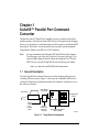
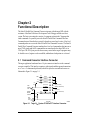
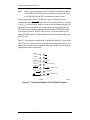
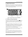
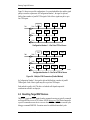
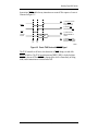
Order this document by
DSPCOMMPARALLELUM/D
Rev. 1.1, 07/1999
Suite56™ Parallel Port
Command Converter User’s Manual
Motorola, Incorporated
Semiconductor Products Sector
6501 William Cannon Drive West
Austin TX 78735-8598
© Copyright Motorola, Inc., 1999. All rights reserved.
This document contains information on a new product.
Motorola reserves the right to make changes without further notice to any products herein. Motorola makes no
warranty, representation or guarantee regarding the suitability of its products for any particular purpose, nor does
Motorola assume any liability arising out of the application or use of any product or circuit, and specifically disclaims
any and all liability, including without limitation consequential or incidental damages. “Typical” parameters which may
be provided in Motorola data sheets and/or specifications can and do vary in different applications and actual
performance may vary over time. All operating parameters, including “Typicals” must be validated for each customer
application by customer’s technical experts. Motorola does not convey any license under its patent rights nor the
rights of others. Motorola products are not designed, intended, or authorized for use as components in systems
intended for surgical implant into the body, or other applications intended to support life, or for any other application in
which the failure of the Motorola product could create a situation where personal injury or death may occur. Should
Buyer purchase or use Motorola products for any such unintended or unauthorized application, Buyer shall indemnify
and hold Motorola and its officers, employees, subsidiaries, affiliates, and distributors harmless against all claims,
costs, damages, and expenses, and reasonable attorney fees arising out of, directly or indirectly, any claim of
personal injury or death associated with such unintended or unauthorized use, even if such claim alleges that
Motorola was negligent regarding the design or manufacture of the part.
Motorola and
are registered trademarks of Motorola, Inc. Motorola, Inc. is an Equal Opportunity/Affirmative
Action Employer.
OnCE and Mfax are trademarks and/or registered trademarks of Motorola, Inc. in the United States and other
countries.
All other tradenames, trademarks, and registered trademarks are the property of their respective owners.
Suite56™ Parallel Port Command Converter
1
Functional Description
2
1
Suite56™ Parallel Port Command Converter
2
Functional Description
Table of Contents
Chapter 1
Suite56™ Parallel Port Command Converter
1.1
General Description . . . . . . . . . . . . . . . . . . . . . . . . . . . . . . . . . . . . . . . . . . . . . . . 1-1
1.2
Operating Environment . . . . . . . . . . . . . . . . . . . . . . . . . . . . . . . . . . . . . . . . . . . . 1-2
1.2.1
Windows PC Requirements . . . . . . . . . . . . . . . . . . . . . . . . . . . . . . . . . . . . . . 1-2
Chapter 2
Functional Description
2.1
2.2
2.3
2.4
Command Converter Interface Connector . . . . . . . . . . . . . . . . . . . . . . . . . . . . . .
Multiple Target Connections . . . . . . . . . . . . . . . . . . . . . . . . . . . . . . . . . . . . . . . .
TCK Drive and Timing Considerations . . . . . . . . . . . . . . . . . . . . . . . . . . . . . . . .
Resetting Target DSP Devices . . . . . . . . . . . . . . . . . . . . . . . . . . . . . . . . . . . . . . .
Motorola
Table of Contents
2-1
2-3
2-3
2-4
v
vi
Suite56TM Parallel Port Command Converter User’s Manual
Motorola
List of Figures
1-1
Target System Configuration . . . . . . . . . . . . . . . . . . . . . . . . . . . . . . . . . . . . . . . . 1-1
1-2
Target Circuit Configuration . . . . . . . . . . . . . . . . . . . . . . . . . . . . . . . . . . . . . . . . 1-2
2-1
Target VDD System JTAG/OnCE™ Interface Connector . . . . . . . . . . . . . . . . . . 2-1
2-2
Target Interface Module’s 14-Pin JTAG/OnCE Connector. . . . . . . . . . . . . . . . . 2-2
2-3
Multiple JTAG Target Connections (Serial Method) . . . . . . . . . . . . . . . . . . . . . 2-3
2-4
Multiple JTAG Connectors (Parallel Method). . . . . . . . . . . . . . . . . . . . . . . . . . . 2-4
2-5
Reset JTAG Device with RESET Signal . . . . . . . . . . . . . . . . . . . . . . . . . . . . . . . 2-5
Motorola
List of Figures
vii
viii
Suite56TM Parallel Port Command Converter User’s Manual
Motorola
Chapter 1
Suite56™ Parallel Port Command
Converter
The Motorola Suite56™ Parallel Port Command Converter is an interface device that,
with the assistance of the Motorola Suite56 DSP Software Development Tools Debugger,
allows you to send and receive information from your host system to your Motorola DSP
based system. The interface is from the parallel port on your host system, through the
Target Interface Module, to the DSP via a JTAG connection.
Note:
For more information on the Motorola DSP Suite56 Software Development
Tools Debugger, refer to the Suite56 Software Development Debugger User's
Manual from the Motorola Suite56 Software Development Tools CD or the
DSP Tools web site on the World Wide Web at the following web address:
http://www.motorola.com/SPS/DSP/tools/documentation
1.1 General Description
The Suite56 Parallel Port Command Converter is used for designing, debugging, and
evaluating DSP-based systems. Figure 1-1 shows how the Command Converter can be
connected in Target System configuration and used as a hardware evaluation tool or as a
host software accelerator.
Host System
14-Pin Ribbon
JTAG Cable
User Application
Circuits
Motorola DSP
25-Pin
Parallel
Port
Extender
Cable
Suite56
Parallel Port
Command
Converter
Application Development
Module (ADM)
AA2035
Figure 1-1. Target System Configuration
Motorola
Suite56™ Parallel Port Command Converter
1-1
Operating Environment
Figure 1-2 illustrates how the Suite56 Parallel Port Command Converter can be used as a
connection to your target system in which the hardware or software needs debugging. The
target hardware must have an access point for the14-pin JTAG ribbon cable, that may be
as simple as a 2-row × 7-set of test points.
25-Pin
Parallel Port
Extender
Cable
Host System
Suite56
Parallel Port
Command
Converter
14-Pin Ribbon
JTAG
Cable
14-Pin
2×7
Connector
A Chain of
up to 24
Target
Devices
Target
AA2036
Figure 1-2. Target Circuit Configuration
The Suite56 Parallel Port Command Converter provides a physical link between the host
system and the target via a parallel port connection on the host machine. This link
translates the high-level debugger commands into JTAG signals and OnCE commands
that enable the host system to reset, interrupt, and send commands to the target DSP.
1.2 Operating Environment
The Motorola DSP Suite56 Software Development Tools used for this Suite56 Parallel
Port Command Converter supports only the Windows PC.
1.2.1 Windows PC Requirements
The minimum hardware requirements for using the Motorola DSP Suite56 Software
Development Tools Debugger on a Windows PC include the following:
1-2
•
Windows PC (Pentium® class processor, or higher)
•
Windows® 95 operating system with 16 Mbytes of RAM, Windows® 98 or
Windows NT® 4.0 operating system with 32 Mbytes of RAM,
•
CD-ROM drive
•
Hard drive with 50 Mbytes of free space
•
Mouse and keyboard
•
Parallel port
Suite56TM Parallel Port Command Converter User’s Manual
Motorola
Chapter 2
Functional Description
The Suite56 Parallel Port Command Converter interacts with the target DSP with the
assistance of the Suite56 Software Development Tools Debugger and the user's host
system. The host system interface consists of a program written in the C language that
sends commands via a parallel port to the Suite56 Parallel Port Command Converter.
Commands entered from the host system's keyboard are parsed, and a series of low-level
command packets are sent to the Suite56 Parallel Port Command Converter. The Suite56
Parallel Port Command Converter translates these low-level command packets into one or
more JTAG signals and OnCE commands that are transferred to the target DSP via its
JTAG port. The JTAG port provides the necessary control to the target so programs may
be loaded or saved, registers read or modified, and hardware breakpoints set or cleared.
2.1 Command Converter Interface Connector
The target application board must have a 14-pin connector to interface to the command
converter controller. This interface comprises eight signals and three ground connections
on a 7-row × 2-column male pin header, which are spaced on one-tenth inch centers as
illustrated in Figure 2-1 on page 2-1.
10K
GND
VCC
GND
Vcc
10K
10K
10K
DSP
RESET
PIN
TARGET
RESET
CIRCUIT
DSP
TRST
PIN
TDI/DSI
1
2
3
4
TCK/DSCK
5
6
GND
(No Connect)
7
8
KEY (No Connect)
9
10
TARGET VDD
11
12
DEZ
13
14
TDO/DSO
CC_RESET
VCC
Vcc
10K
TMS0 (For JTAG Devices)
(No Connect)
TRST (For JTAG Devices)
(For JTAG Devices)
10K
TOP VIEW
AA2037
Figure 2-1. Target VDD System JTAG/OnCE™ Interface Connector
Motorola
Functional Description
2-1
Command Converter Interface Connector
Note:
Figure 3-1 may not represent the exact JTAG/OnCE configuration needed for
every DSP due to possible differences in internal resistors on the pins. Please
see the Data Sheet for your DSP for information on internal resistors.
Since the target system will have a resident reset circuit, an AND gate-in-series is
recommended with the CC_RESET signal. This will allow the target DSP to be reset with
a valid VOL level from either the target-reset circuit or from the command converter. The
pull-down resistors are provided to prevent false signals from being propagated to the
JTAG/OnCE circuit when the test data input/debug serial input (TDI/DSI) and test data
clock/debug serial clock (TCK/DSCK) lines are active. The test data out/debug serial
output (TDO/DSO) pull-up is designed to deassert the Debug Acknowledge signal from
the OnCE circuit
Figure 2-2 is the connector coming from the Target Interface Module via a 14-pin ribbon
cable. When viewed with pin 8 (keyed) on the right side, this plug connector has all odd
numbers on the left side and all even numbers on the right side when viewed from the top.
Spacing between pins is one-tenth inch.
.
TDI/DSI
TDO/DSO
TCK/DSCK
No Connect
1
2
3
4
5
6
7
8
9
10
11
12
CC_RESET
TARGET VDD
DEZ
13
14
(For JTAG/OnCE Devices)
GND
KEY (No Connect)
TMS0 (For JTAG Devices)
No Connect
TRST (For JTAG Devices)
TOP VIEW
AA2038
Figure 2-2. Target Interface Module’s 14-Pin JTAG/OnCE Connector
2-2
Suite56™ Parallel Port Command Converter User’s Manual
Motorola
TCK Drive and Timing Considerations
2.2 Multiple Target Connections
Multiple target devices may be connected in series, allowing a single command converter,
JTAG/OnCE connector to control multiple devices, as in Figure 2-3. Data flows from the
JTAG host, into each JTAG implementation through TDI, out through TDO and into TDI
in the next chip, eventually returning to the JTAG host.
RESET
TRST
TDO
TRST RESET
TDI TDO
TCK TMS
TRST RESET
TDI TDO
TCK TMS
TRST RESET
TDI TDO
TCK TMS
TRST RESET
TDI TDO
TCK TMS
TRST RESET
TDI
TDO
TCK TMS
TRST RESET
TDI TDO
TCK TMS
TDI
TCK
TMS
Maximum of 4 Loads on
TCK Circuits
Buffer—74HCT244
or Similar
AA2039
Figure 2-3. Multiple JTAG Target Connections (Serial Method)
2.3 TCK Drive and Timing Considerations
The signals from the command converter are TDO, TCK and TMS, and TRST. The TCK
signal requires fast rise and fall times dictated by the TCK pin timing specification, and
consequently attention must be given to the drive capability of the circuits driving this
signal.
When driving the TCK and TMS circuits with a large number of target devices, the user
must pay attention to the rise and fall times of TCK and TMS. Excessive capacitance may
cause communication problems when driving a single circuit that connects multiple TCK
or multiple TMS input pins. Excessive capacitance can also cause communication
problems with a single circuit connecting multiple TMS input pins.
Acceptable transition times may be achieved for TCK and TMS by driving no more than
four JTAG inputs from each buffered output. This may be achieved with two
configurations.
Figure 2-3 shows one method. Here (in effect) one signal connects each of the TCK
inputs, and one signal connects each of the TMS inputs. A buffer is placed in the circuit
after each fourth input at most, to restore the signal quality for subsequent inputs. The
propagation delay of the buffer is not significant.
Motorola
Functional Description
2-3
Resetting Target DSP Devices
Figure 2-4 shows two possible configurations of a second method that also enables signal
quality to meet the requirements. In Configuration Number 1, the signal is split and
buffered into a number of parallel TCKn signals. Each of these signals may drive up to
four TCK inputs.
TCK
TCK1
TCK2
TCKn
TCK
TCK
TCK
TCK
TCK
TCK
TCK
TCK
TCK
TCK
TCK
Configuration Number 1 —Fan Out of TCK at Source
TMS
TMS1
TMS2
TMSn
TMS
TMS
TMS
TMS
TMS
TMS
TMS
TMS
TMS
TMS
TMS
AA2040
Configuration Number 2 —Fan Out of TMS at Source
Figure 2-4. Multiple JTAG Connectors (Parallel Method)
In Configuration Number 2, the signal is split and buffered into a number of parallel
TMSn signals. Each of these signals may drive up to four TMS inputs.
Each method is equally valid. The choice of methods will depend on practical
considerations related to each project.
2.4 Resetting Target DSP Devices
The RESET signal and TRST signals from the command converter are typically connected
to all target DSP devices on a JTAG chain. All DSP devices on a JTAG chain connected to
a specific command converter device are reset when RESET and TRST are asserted by the
debugger command FORCE R. Execution control is established immediately after
2-4
Suite56™ Parallel Port Command Converter User’s Manual
Motorola
Resetting Target DSP Devices
deassertion of TRST and before any instructions are executed. This sequence of events is
illustrated in Figure 2-5.
1
(1) Command Converter
Asserts RESET. All
Targets Enter Reset.
1
(2) Asserted TRST
(2A) Deasserted TRST
2
(3) JTAG Instruction
DEBUG_REQUEST is
Loaded.
3
(4) Command Converter
Releases RESET. Targets
Exit Reset in Debug Mode.
RESET
TRST
Instruction
Register
DEBUG_REQ
1
(1)
(2)
2
(2A)
(3)
3
(4)
AA2041
Figure 2-5. Reset JTAG Device with RESET Signal
The JTAG controller is still active after deassertion of TRST during reset and while
RESET is held low. The JTAG special instruction DEBUG_REQ is clocked in before
RESET is deasserted. When RESET is deasserted, the device is immediately in Debug
mode, and no instructions are executed in the DSP.
Motorola
Functional Description
2-5
Resetting Target DSP Devices
2-6
Suite56™ Parallel Port Command Converter User’s Manual
Motorola
Suite56™ Parallel Port Command Converter
1
Functional Description
2
1
Suite56™ Parallel Port Command Converter
2
Functional Description