1
AN2110/D:
Rev. 0, 2/2001
MOTOROLA
Semiconductor Products Sector Engineering Bulletin
By James M. Montgomery
This document describes the development and implementation of
a 10-band stereo equalizer programming example on the
Motorola DSP56311 Evaluation Module (EVM). It provides an
example of how to use readily available development tools to
develop complex code for the DSP56311EVM. It also discusses
how to program the enhanced filter coprocessor (EFCOP) in
Multichannel mode.
The DSP56311EVM is a low-cost hardware platform that serves
as a hardware reference design for system and board designers
using the DSP56311. It is also a very flexible platform for
developing DSP56311 code. Software engineers can download
software to on-device or on-board RAM, then run and debug it.
The DSP56311EVM features:
•
DSP56311 24-bit digital signal processor
•
FSRAM for expansion memory and flash memory for
stand-alone operation
•
16-bit CD-quality audio codec
•
Command converter circuitry
For details on the DSP56311EVM, consult the DSP56311EVM
Product Preview (DSP56311EVMP/D) and the DSP56311EVM
User’s Manual (DSP56311EVMUM/D).
It is assumed that you already have access to the available
Motorola DSP56311 documentation, which is located on the
following Motorola DSP World Wide Web site:
http://www.mot.com/SPS/DSP/documentation
Contents
1 Filter Design ............................... 2
2 Development Environment ....... 5
2.1
2.2
2.3
2.4
Personal Computer Running
Windows NT® 4.0........................... 5
Suite56 Parallel Command
Converter......................................... 5
Interfacing the PC to the
DSP56311EVM............................... 6
Useful Debugging Techniques ........ 7
3 Implementation of 10-Band
Stereo Equalizer 7
3.1
3.1.1
3.1.2
3.1.3
Program Flow and Functionality ..... 7
Equalizer Filter and Volume Gain... 8
Stage 1: DSP Initialization ............ 10
Stage 2: Codec/ESSI Initialization
and Operation................................. 10
3.1.4 Stage 3: SCI Initialization and
Operation ....................................... 12
3.1.5 Stage 4: EFCOP Memory
Initialization and DMA Setup........ 13
3.1.6 Stage 5: Equalizer Knob Value
Initialization................................... 17
3.1.7 Stage 6: Set up Registers R0 to R7 17
3.1.8 Stage 7, 8, 10, and 12: Codec
Operation ....................................... 18
3.1.9 Stage 9 and 11: Process
Left/Right Input ............................. 19
3.1.10 Stage 13 and 14: Setting Knob
and Main Volume Gain Values ..... 21
4 Equalizer Graphical User
Interface (GUI) 23
4.1
4.2
4.2.1
4.2.2
4.2.3
GUI Operation ............................... 23
GUI Development.......................... 24
Equalizer Form .............................. 24
Frequency Table Form................... 25
Communications Port Settings
Form............................................... 25
5 Using the EFCOP in
Multichannel Mode ................. 25
5.1
5.2
EFCOP Registers ........................... 26
EFCOP Programming for
Multichannel Mode27
5.2.1 FIR Filter Type .............................. 27
5.2.2 IIR Filter Type ............................... 28
5.2.3 Memory Configuration .................. 29
6 Coefficients and Gain Table
Files ........................................... 30
7 References ................................ 35
© Motorola, Inc. 20001
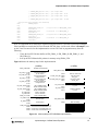
Implementing a 10-Band Stereo Equalizer
Implementing a 10-Band Stereo
Equalizer on the DSP56311 EVM
Board
Filter Design
1
Filter Design
The 10-band stereo equalizer is constructed using 10 digital IIR bandpass filters in parallel for each stereo
audio channel. The on-board codec samples the incoming audio stream at 48,000 Hz. The center
frequencies for these filters lie between 0 Hz to fs/2 (where fs is the sample frequency of 48,000 Hz).
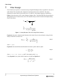
Figure 1 shows the passive RCL circuit forming a bandpass filter. The digital IIR Filter discussed later in
this application note is based on this circuit. The s-domain analysis of the second-order bandpass analog
filter is also shown.
Vi
Vo
L
C
R
Vo
R
------- = --------------------------------------------------------Vi
1
R + j ( 2πf )L + -------------------j ( 2πf )C
Figure 1. Analog Bandpass Filter and Voltage Divider Analysis
Equation 1 shows the s-domain transfer function of the circuit. H(s) is derived from the voltage divider
analysis of the RCL network to be:
Vo
Rs
H ( s ) = ------ = -------------------------------Vi
1
Rs + Ls 2 + ---C
Eqn. 1
where s = j ( 2πf ) .
Equation 2 shows the bilinear transformation between the s-plane and the z-plane:
2 1 – z –1-
s = --- --------------T 1 + z – 1
Eqn. 2
where z = e jθ , θ = ωT = ( 2πf ) ( 1 ⁄ f s ) , and T is the sample period ( 1 ⁄ f s ) .
Using Equation 2, the z-plane transfer function is found from Equation 1:
α ( 1 – z –2 )
H ( z ) = -----------------------------------1--– γz –1 + βz –2
2
2
Implementing a 10-Band Stereo Equalizer
Eqn. 3
Filter Design
With Equation 3, the coefficients for each filter are calculated using the following three equations:
θo
1 – tan -------
2Q
1
β = --- ------------------------------2
θ
1 + tan ------o-
2Q
Eqn. 4
1
γ = --- + β cos θ o
2
Eqn. 5
1
α = --- – β ⁄ 2
2
Eqn. 6
where Q = f o ⁄ ( f 2 – f 1 ) and θ o = 2π ( f o ⁄ f s ) . The value f o is the center frequency of the bandpass filter, f 1 and
f 2 are the half-power points (where the gain is equal to 1 ⁄ ( 2 ) ), and f s is the sample frequency. These
equations are approximations for center frequencies less than f s ⁄ 8 (or 6000 Hz).1 To implement the
transfer function from Equation 3 as a digital IIR Filter, it must be transformed to a difference equation in
the discrete time domain. Equation 7 shows this difference equation, and Figure 2 shows its
representation as a network diagram.
y ( n ) = 2 { α [ x ( n ) – x ( n – 2 ) ] + γy ( n – 1 ) – βy ( n – 2 ) }
Eqn. 7
α
x(n)
y(n)
2
z –1
γ
z –1
y( n – 1 )
Σ
z –1
x( n – 2 )
–α
z –1
–β
y(n – 2)
Figure 2. Bandpass IIR Filter Network Diagram
At each sample period, a left and right sound byte is fed to the 10 filters in parallel (see Figure 3). After
each respective bandpass filter eliminates the frequencies not in its range, each output ( y1 ( n ) → y10 ( n ) ) is
scaled by an output gain. This gain value ranges from 0 to 1. The results of the ten filters are then summed
together and outputted. This process allows one to selectively remove, or limit, the gain of a particular
frequency range from the sound source.
1. See the application note entitled Implementing IIR/FIR Filters with Motorola’s DSP56000 DSP (APR7/D).
Implementing a 10-Band Stereo Equalizer
3
Filter Design
y1 ( n )
31 Hz
y2 ( n )
62 Hz
125 Hz
250 Hz
x(n)
500 Hz
1 kHz
y3 ( n )
y4 ( n )
y5 ( n )
Σ
y6 ( n )
y(n)
y7 ( n )
2 kHz
y8 ( n )
4 kHz
y9( n )
8 kHz
16 kHz
y 10 ( n )
Figure 3. IIR Equalizer Data-Flow Diagram
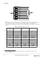
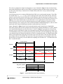
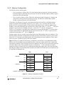
Table 1 shows the 10 center frequencies chosen for this programming example. The coefficients for the
center frequencies less than f s ⁄ 8 (or 6000 Hz) were found using equations 4–6 in Section 1 . The
coefficients for the center frequencies above 6000 Hz were found using more exact equations. 2 Q is chosen
to be 1.4.
Table 1. Digital IIR Bandpass Coefficients
Center
Frequency
α
β
γ
31 Hz
0.000723575
0.49855285
0.998544628
62 Hz
0.001445062
0.497109876
0.997077038
125 Hz
0.002904926
0.494190149
0.994057064
250 Hz
0.005776487
0.488447026
0.987917799
500 Hz
0.011422552
0.477154897
0.975062733
1000 Hz
0.02234653
0.455306941
0.947134157
2000 Hz
0.04286684
0.414266319
0.88311345
4000 Hz
0.079552886
0.340894228
0.728235763
8000 Hz
0.1199464
0.2601072
0.3176087
16000 Hz
0.159603
0.1800994
-0.4435172
2. For a full analysis, see the application note entitled Digital Stereo 10-Band Graphic Equalizer Using the
DSP56001 (APR2/D).
4
Implementing a 10-Band Stereo Equalizer
Development Environment
2
Development Environment
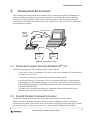
This section describes the development environment for the 10-band stereo equalizer (see Figure 4). It
outlines the hardware and software requirements; describes how to establish the physical connection
between the PC and the DSP56311 EVM board; and lists the steps for compiling, downloading, and
running code on the DSP56311 EVM board. Once you complete these steps, you are ready to implement
the 10-band stereo equalizer.
Serial Port Cable
Suite56
Sui te56
parallel
Parall el
command
Command
converter
Converter
Paralle l Port Cable
JTag Connecter
PC
PC
DSP56311EVM
DSP56311EVM
PC
Stereo
Input
Input
Stereo
Stereo
Output
Output
Figure 4. Development Setup
2.1 Personal Computer Running Windows NT® 4.0
The following programs should be running on your personal computer:
•
Codewright for Windows. Programmer’s text editor used to create and modify files. Note that other
text editors can also be used.
•
Command Prompt. DOS-style terminal used to run the asm56300 compiler.
•
Suite56 DSP56300 Software Development Tools. Free Motorola DSP tools to compile and link
DSP assembly code. The hardware debugger, ads56300, has a GUI interface that communicates
with the EVM Board through the parallel port command converter. It also downloads and executes
code on the DSP56311EVM.
•
Visual Basic® 4.0. Programming language for creating the equalizer GUI that allows you to
change the gain values for the various equalizer bands.
2.2 Suite56 Parallel Command Converter
The parallel command converter provides the physical connection between the PC and the
DSP56311EVM. Its parallel port interface connects to the PC. In addition, its female 14-pin header
connects the device to the JTAG/OnCE Port (J2) on the DSP56311EVM. For details on this device, consult
the Suite56 Parallel Port Command Converter User’s Manual (DSPCOMMPARALLELUM/D).
Implementing a 10-Band Stereo Equalizer
5
Development Environment
The jumper settings on the DSP56311EVM are listed in Table 2. For details on how to set up the jumpers
for the desired functionality, see the DSP56311EVM User’s Manual (DSP56311EVMUM/D).
Table 2. Jumper Setting on the DSP56311 EVM Board
Number
Function
Description
J1
Boot Mode Select
HI08 bootstrap in MC68302 bus mode
J3
FSRAM Memory Configuration Option
Unified memory map
J4
SCI Header Pinout
Connects serial port connector signals RxD and TxD to
the DSP SCI port
J5
SCI Port Clock
Connects on-board 156.3 kHz oscillator to the SCI port
SCLK input (used for baud rate generation)
J6
On-board JTAG Enable/Disable Option
On-board command converter disabled
J7
ESSI0 Header Pinout
Selects the DSP ESSI0 port interface for use with an
on-board codec
J8
CS4218 Sampling Frequency Selection
Selects 48 kHz sample rate for the codec
J9
ESSI1 Header Pinout
Selects DSP ESSI1 port interface for use with an
on-board codec
J10
Core Current Measurement Jumper
Connected jumper that applies power to the DSP core
The Line IN jack on the DSP56311EVM connects to the headphone jack of the PC. The PC provides the
sound source for the DSP56311EVM. A pair of headphones or stereo speakers can connect to the
Headphone OUT/Line OUT jack to listen to the filtered sound source.
2.3 Interfacing the PC to the DSP56311EVM
Following are the steps to compile, download and run the code on the DSP56311EVM. It is assumed that
you are using the GUI version of ADS56300 (part of the Suite56 Motorola DSP software development
tools):
1. The stereo.asm file is the main assembly file of the project. Using the command prompt, change to
the directory where the project files are stored.
2. At the prompt, type: asm56300 -a -b -l stereo.asm.
Two output files are created. Stereo.lst contains a listing of the code, and stereo.cld is the
executable to be downloaded to the DSP56311EVM. There may be a few warning when you compile
the code. These warnings tell you of pipeline stalls located in the code. They have no effect on the
operation of the code.
3. Using the ADS56300 GUI, reset the 56311EVM.
4. Under File → Load → Memory COFF, select the desired file (stereo.cld). Press Apply to load the
file into memory.
5. Select GO (or type go into the Command window).
6
Implementing a 10-Band Stereo Equalizer
Implementation of 10-Band Stereo Equalizer
You should know about the following ADS56300 GUI windows:
•
Command. Allows the user to type line commands.
•
Core Registers. Displays the state of the core registers. The values can also be modified.
•
EFCOP Registers. Displays the state of the EFCOP registers. The values can also be modified.
•
Assembly. Displays the assembly code loaded in the DSP56311 program memory.
•
X Memory. Displays the X-data Memory in the DSP56311.
•
Y Memory. Displays the Y-data Memory in the DSP56311.
2.4 Useful Debugging Techniques
The breakpoint feature can be very useful. Software breakpoints stop at a particular instruction in program
memory. Hardware breakpoints allow you to examine the effects of the DSP56311. For example, a
breakpoint can be set up when a DMA channel writes data to one of the EFCOP registers in Y memory.
This allows you to view the state of the EFCOP after each sample is written to it. Hardware breakpoints are
particularly helpful when EFCOP operation needs to be verified.
3
Implementation of 10-Band Stereo Equalizer
There are numerous ways to implement the 10-band stereo equalizer using the DSP56311EVM. The
examples in this section show how to implement two versions of the equalizer. The overall functionality of
both versions is identical. The main differences between the versions lie in how the DSP56311 resources
are used. The two versions of the equalizer are compared in terms of:
•
Program Flow and Functionality. The general flow serves as a template for designing each
specific implementation. Pertinent information includes how the DSP is initialized, what the main
interrupt sources are, how they are configured, and how they are handled. After examining these
features, you should have a good idea at how the overall program is structured.
•
DSP56311 Core Implementation. How to process the 10 bandpass filters using the DSP56300
core. The memory map and register usage must also be considered.
•
EFCOP and DMA Implementation. How to process the 10 bandpass filters using the EFCOP in
Multichannel mode and the DMA controller. The DSP56300 core is minimally used to set up the
peripherals. The memory map, register usage, and peripheral setup must also be considered.
3.1 Program Flow and Functionality
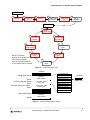
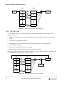
The general program flow of the 10-band stereo equalizer occurs in 14 stages (see Figure 5). All but four
of these stages (4, 6, 9, and 11) generally apply to any implementation. The first six stages initialize the
DSP56311EVM hardware and software buffers in memory:
•
Stage 1: Initialize the DSP56311. Set the clock frequency and bus interface.
•
Stage 2: Initialize ESSI0 and ESSI1 to interface with the codec.
•
Stage 3: Initialize the SCI to interface with an RS-232 port.
•
Stage 4:
Implementing a 10-Band Stereo Equalizer
7
Implementation of 10-Band Stereo Equalizer
a. (DSP56311 core implementation): Set up the Data Sample and Filter Coefficient memory
buffers. These data buffers reside in X and Y memory, respectively
b. (EFCOP and DMA Implementation): Set up EFCOP memory and initialize the DMA
controllers.
•
Stage 5: Set the equalizer knob values to a preset level.
•
Stage 6: Set up the values in registers R0 to R7.
The last eight stages are part of an infinite loop to process the data received and transmitted through the
codec:
•
Stage 7: Frame sync for the codec.
•
Stage 8: Get voice data from the receive buffer.
•
Stage 9: Process the LEFT voice data using the 10 Bandpass filters.
•
Stage 10: Store the LEFT voice data to transmit buffer.
•
Stage 11: Process the RIGHT voice data using the 10 Bandpass filters.
•
Stage 12: Store the RIGHT voice data to transmit buffer.
•
Stage 13: Using the equalizer knob values, adjust the gain values for each of the 10 bandpass
filters.
•
Stage 14: Using the equalizer knob value that sets the main volume, adjust the main volume
settings of the codec.
3.1.1 Equalizer Filter and Volume Gain
After each of the 10 digital IIR bandpass filters in the 10-band stereo equalizer eliminates the frequencies
not in its range, the output is scaled by its respective output gain. The 10 gain values (and main volume)
are determined by user-settable values called equalizer knob values.3 The equalizer knob values consist of
eleven 8-bit values received through the Serial Communication Interface (SCI) and placed into a
predetermined space in Y memory (see Figure 6). The least significant five bits of the first ten knob values
are used to select one out of 32 values in the filter gain table, ranging from –0.2 to 0.999 (see Example 16
on page -33). The least significant five bits of the last knob value are used to select 1 out of 32 values in the
volume gain table, which are used to configure the volume setting in the codec (see Example 17 on page
-34). Using interrupts, the SCI constantly updates the equalizer knob values in Y memory. In Stage 13, the
knob values are used to update the runtime gain values. The 5-bit knob values function as indexes into the
filter and volume Gain tables. The run-time gain values are then used in Stages 9 and 11 when the voice
data is filtered. This process continually repeats.
3. The equalizer GUI is used to set the equalizer knob values.
8
Implementing a 10-Band Stereo Equalizer
Implementation of 10-Band Stereo Equalizer
Program Start
1
DSP Init.
2
Codec/ESSI
Init
4
EFCOP/Data
Buffer Init
3
SCI Init
6
5
Knob Value
Init
Set up
Registers
Loop Start
7
Codec
Frame Sync
14
8
Get data from
RX Buffers
Set Main
Volume
13
9
Process LEFT
Input
Set Band
Gain Values
12
Send RIGHT
Input
NOTE: The stages
depicted in the boxes with
thick borders generally
apply to any implementation
of the 10-band stereo equalizer.
10
Send LEFT
Input
11
Process Right
Input
Figure 5. General Program Flow
(Y-MEM)
KNOB_BASE: $0100
...
$010A
FILTER_GAIN_TBL: $0200
...
$021F
VOLUME_GAIN_TBL: $0300 ...
$031F
Equalizer
Knob Values
Filter Gain Table
‘filter_gain’
Volume Gain Table
‘volume_gain’
Filter Coefficients
GAIN_BASE: $2A00
...
$2A0A
31 Hz Knob Val
62 Hz Knob Val
125 Hz Knob Val
250 Hz Knob Val
500 Hz Knob Val
1000 Hz Knob Val
2000 Hz Knob Val
4000 Hz Knob Val
8000 Hz Knob Val
16000 Hz Knob Val
Main VOL Knob Val
(X-MEM)
KNOB_VAL
Runtime
Gain Values
Figure 6. Knob and Gain Memory Areas
Implementing a 10-Band Stereo Equalizer
9
Implementation of 10-Band Stereo Equalizer
3.1.2 Stage 1: DSP Initialization
The first stage of the code, shown in Example 1, initializes the following DSP memory address locations:
•
INIT_PCTL. Written to the Phase Lock Loop Control Register (PCTL) to set up the DSP56300
core operating frequency.
•
INIT_BCR. Written to the Bus Control Register (BCR) to control the external bus activity and bus
interface unit operation.
•
START. Marks the start of the program in program memory.
Example 1. DSP Initialization
;******************************************************************************
nolist
include ’ioequ.asm’
include ’intequ.asm’
include ’ada_equ.asm’
include ’vectors.asm’
list
INIT_PCTL
INIT_BCR
EQU
EQU
$040006 ; Fcore=fcrystal*MF=12.288MHz*7=86 MHz
$012421
org
p:$400
START
;-------------------------; DSP Initialization
;-------------------------movep
#INIT_PCTL,x:M_PCTL
movep
#INIT_BCR,x:M_BCR
ori
#3,mr
movec
#0,sp
move
#0,omr
;
;
;
;
;
PLL 7 X 12.288 = 86.016MHz
AARx - 1 wait state
mask interrupts
clear hardware stack pointer
operating mode 0
3.1.3 Stage 2: Codec/ESSI Initialization and Operation
The second stage of the code, shown in Example 2, sets up the codec on the DSP56311 EVM Board. The
receive and transmit buffer pointers are set up first. Then the ada_init procedure sets up the codec by
initializing the ESSI0 and ESSI1 registers. For details, refer to Programming the CS4218 CODEC for Use
With DSP56300 Devices (AN1790/D).
Example 2. Codec/ESSI Initialization
;-------------------------; Codec Initialization
;-------------------------move
#RX_BUFF_BASE,x0
move
x0,x:RX_PTR
move
#TX_BUFF_BASE,x0
move
x0,x:TX_PTR
jsr
ada_init
10
; Initialize the rx pointer
; Initialize the tx pointer
; Initialize codec
Implementing a 10-Band Stereo Equalizer
Implementation of 10-Band Stereo Equalizer
The codec is configured to sample incoming data at a rate of 48,000 Hz. Figure 7 shows the data format
between the ESSI interface and the codec. ESSI0 is configured for Network mode with two time slots. Slot
0 of the 32-bit frame always contains the Left Channel Word, while Slot 1 always contains the Right
Channel Word.
Six ESSI0 interrupt service routines (ISRs) handle the ESSI0 receive and transmit interrupts. These ISRs
are located in the ada_init.asm file. A receive interrupt occurs at the end of each time slot, after each
channel is serially shifted into the ESSI0 Receive Shift Register and then transferred to the Receive Data
Register. The receive interrupt service routines place each word in the receive buffers into X memory (see
Figure 7). The 16-bit channel words are placed into the 16 most significant bits of the 24-bit memory
word. The lower 8 bits are cleared. A transmit interrupt occurs at the beginning of each time slot. The
transmit interrupt service routines place each word into the ESSI0 Transmit Data Register, where it is then
transferred to the Transmit Shift Register and then serially shifted out of the DSP.
Stages 7 through 12 (Figure 5) take the left and right channel words from the Receive Data Buffer
(RX_BUFF_BASE), process them, and place the result into the Transmit Data Buffer (TX_BUFF_BASE)
to be transmitted during the next codec data frame. T1 and T2 in Figure 7 represents the maximum time
allowed to process each channel in order to be transmitted correctly during the following time frame. The
Left Channel (T1) must be processed from the rising edge of the frame sync to the falling edge of the frame
sync and placed into the Transmit Data Buffer in order to be transmitted on time. The Right Channel (T2)
must be processed from the rising edge of the frame sync to the end of slot 0 of the next time frame and
placed into the Receive Data Buffer. The restriction of the processing time for each channel is due to the
design. With a core frequency of 86.016 MHz and a sampling rate of 48 kHz, T1 = 1794 DSP clocks and
T2 = 59,198 DSP clocks.
Frame 32-bits
SSYNC
SDIN
STOUT
Left Channel Word 0
Right Channel Word 0
Left Channel Word
Right Channel Word
Slot 0
Slot 1
16-bits
16-bits
Left Channel Word
Right Channel Word
Left Channel Word 0
Right Channel Word 0
T1
T2
(X-MEM)
RX_BUFF_BASE:
TX_BUFF_BASE:
00000000
00000000
00000000
00000000
Left Channel Word
Right Channel Word
Left Channel Word
Right Channel Word
23
7
0
Figure 7. Codec Data Format and Layout in Memory
Implementing a 10-Band Stereo Equalizer
11
Implementation of 10-Band Stereo Equalizer
3.1.4 Stage 3: SCI Initialization and Operation
Stage 3 of the code, shown in Example 3, initializes the following memory address locations:
•
INIT_SCCR. Written to the SCI Clock Control Register (SCCR) to set up the baud rate.
•
INIT_SCR. Written to the SCI Control Register (SCR) to control the serial interface operation.
The Port E register (PCRE) is also configured to enable the SCI lines. Finally the pointer (KNOB_VAL) to
the equalizer knob values in Y memory is initialized.
Example 3. SCI Initialization
INIT_SCCR
INIT_SCR
EQU
EQU
$002010 ; baud = Fcore/[64*(7(SCP)+1)*(CD+1)]
$000b02
;-------------------------; SCI Initialization
;-------------------------movep
#INIT_SCCR,x:M_SCCR
movep
#INIT_SCR,x:M_SCR
movep
#$7,x:M_PCRE
move
#KNOB_BASE,r0
move
r0,x:KNOB_VAL ;
; Initialize SCI
; Initialize the SCI pointer.
The SCI is configured to receive the equalizer knob values from the external PC (or other source). One ISR
handles the SCI receive interrupt. A receive interrupt occurs when a byte is shifted into the SCI Receive
Shift Register and then transferred to the Receive Data Register. The ISR places this byte in one of the
equalizer knob value memory locations to which KNOB_VAL points (see Figure 6). The operation of the
SCI ISR is very simple (as shown in the top half of Figure 8).
1. It saves a few core registers to the system stack.
2. It reads the data byte from the SCI Receive Data Register.
3. The character “Enter” (hex value 0xd) is used to reset the table pointer (KNOB_VAL) to the equalizer
knob value base (KNOB_BASE).
4. If the character “Enter” is read, KNOB_VAL is set to equal KNOB_BASE. Else if another character is
read, then that character is put at the Y-Memory location pointed to by KNOB_VAL.
5. The core registers are then restored, and the interrupt exits.
In this programming example, the equalizer knob values come from the COM1 or COM2 port of a PC. The
Equalizer GUI that allows the user to set the knob values sends the data pattern shown in the bottom half of
Figure 8.
12
Implementing a 10-Band Stereo Equalizer
Implementation of 10-Band Stereo Equalizer
D
YES
SCI RX IRQ
B
A
Save REGs
to Stack
ENTER
0x0D
Reset PTR
KNOB_VAL=KNOB_BASE
D
C
Read from
SCI RX Buff
Char = 0x0d
??
NO
Put Char into
Knob Table
E
Restore REGs
from Stack
RFI
31 Hz Knob 62 Hz Knob 125 Hz Knob 250 Hz Knob 500 Hz Knob 1 kHz Knob 2 kHz Knob 4 kHz Knob 8 kHz Knob 16 kHz Knob Volume Knob
Char2
Char3
Char4
Char6
Char8
Char11
Char1
Char9
Char5
Char7
Char10
Figure 8. SCI Interrupt Service Routine and Incoming Data Pattern
3.1.5 Stage 4: EFCOP Memory Initialization and DMA Setup
Stage 4 of the code, shown in Example 4, sets up the X and Y memories for this version of the
implementation. The code in program memory does two things.
•
Clears the x(n) and y(n) data buffers at DATA_BASE_L and DATA_BASE_R.
•
Sets up the data buffer pointers in memory using DATA_PTR.
Figure 9 shows the memory map for this implementation. The following areas of memory are specific to
this implementation and have not been discussed in previous sections.
•
DATA_BASE_L and DATA_BASE_R. These two areas in X memory hold the current data values
for x(n) to x(n-2) and y(n) to y(n-2) for all 10 bandpass filters.
•
DATA_PTR. It is necessary to store the pointers to the memory areas. Storing these values in X
memory means that one register can be assigned to save and restore the four data pointers when
they’re needed.
•
COEF_BASE. This area of Y memory contains the α , β , and γ coefficients for each of the 10
bandpass filters.
Implementing a 10-Band Stereo Equalizer
13
Implementation of 10-Band Stereo Equalizer
(X-MEM)
STACK_PTR: $0000
DATA_BASE_L: $1000
...
$1002
$1040
...
$1067
DATA_BASE_R: $1100
...
$1102
$1140
...
$1167
RX_BUFF_BASE: $2800
$2801
TX_BUFF_BASE: $2802
$2803
RX_PTR: $2804
TX_PTR: $2805
KNOB_VAL: $2806
(Y-MEM)
SYSTEM STACK PONTER
x(n) Values for LEFT Channel
y(n) Values for LEFT Channel
x(n) Values for RIGHT Channel
KNOB_BASE: $0100
...
$010A
FILTER_GAIN_TBL: $0200
...
$021F
VOLUME_GAIN_TBL: $0300
...
$031F
Filter Gain Table
‘filter_gain’
Volume Gain Table
‘volume_gain’
y(n) Values for RIGHT Channel
LEFT CHANNEL WORD
RIGHT CHANNEL WORD
COEF_BASE: $1000
...
$101D
Filter Coefficients
‘coeff’
LEFT CHANNEL WORD
RIGHT CHANNEL WORD
Pointer to RX Buffer
Pointer to TX Buffer
Pointer to KNOB TABLE
GAIN_BASE: $2A00
...
$2A0A
DATA_PTR: $2B00
$2B01
$2B02
$2B03
31 Hz Knob Value
...
Main VOL Knob Value
31 Hz Channel Gain
...
Main VOL Setting
Pointer to Yi(n): Left-channel
Pointer to X(n): Left-channel
Pointer to Yi(n): Right-channel
Pointer to X(n): Right-channel
Figure 9. Memory Map for DSP56300 Core Implementation
Example 4. Filter Parameter Setup
org
include
org
include
org
include
y:FILTER_GAIN_TBL
’filter_gain’
y:VOLUME_GAIN_TBL
’volume_gain’
y:COEF_BASE
’coeff’
;;;;IN PROGRAM MEMORY;;;
;-------------------------; Filter Parameter Setup
;-------------------------move
#0,r0
;Clear the x(n) and y(n) Data Buffers
move
#DATA_BASE_L,r3
rep
#$68
move
r0,x:(r3)+
; x:DATA_BASE_L+($00..$02)
; x:DATA_BASE_L+($40..$42)
; x:DATA_BASE_L+($44..$46)
; ....
; x:DATA_BASE_L+($64..$66)
move
rep
move
14
- x(n) left chan.
- y(n) left chan. 31 Hz
- y(n) left chan. 62 Hz
- y(n) left chan. 16 kHz
#DATA_BASE_R,r3
#$68
r0,x:(r3)+
Implementing a 10-Band Stereo Equalizer
Implementation of 10-Band Stereo Equalizer
;
;
;
;
;
x:DATA_BASE_R+($00..$02)
x:DATA_BASE_R+($40..$42)
x:DATA_BASE_R+($44..$46)
....
x:DATA_BASE_R+($64..$66)
- x(n) right chan.
- y(n) right chan. 31 Hz
- y(n) right chan. 62 Hz
- y(n) right chan. 16 kHz
; Setup Filter Data Buffers (and Pointers)
move
#DATA_PTR,r3
nop
move
#DATA_BASE_L+$40,r0
; Yi(n):L-ch
move
r0,x:(r3)+
move
#DATA_BASE_L,r0
; X(n):L-ch
move
r0,x:(r3)+
move
#DATA_BASE_R+$40,r0
; Yi(n):R-ch
move
r0,x:(r3)+
move
#DATA_BASE_R,r0
; X(n):R-ch
move
r0,x:(r3)
at x:DATA_BASE_L+$40
at x:DATA_BASE_L
at x:DATA_BASE_R+$40
at x:DATA_BASE_R
Next, we implement the 10-band stereo equalizer using the DSP56311 EFCOP to process the bandpass
filters and DMA to transfer the DATA to/from the EFCOP. Stage 4 of the code, shown in Example 5, sets
up the X and Y memories for this implementation version. The code in program memory does the
following:
•
Clears the four EFCOP data buffers at FIR_FDBA_L, FIR_FDBA_R, IIR_FDBA_L, and
IIR_FDBA_R.
•
Sets up the EFCOP data buffer pointers in memory using FDBA_PTR.
Figure 10 shows the memory map for this implementation.
(X-MEM)
STACK_PTR: $0000
SYSTEM STACK PONTER
FIR_FDBA_L: $1000
...
$1027
FIR_FDBA_R: $1100
...
$1127
IIR_FDBA_L: $1200
...
$1213
IIR_FDBA_R: $1300
...
$1313
EFCOP FIR Data Buffer
for Left Channel
EFCOP IIR Data Buffer
for Left Channel
VOLUME_GAIN_TBL: $0300
...
$031F
31 Hz Knob Value
...
Main VOL Knob Value
Filter Gain Table
‘filter_gain’
Volume Gain Table
‘volume_gain’
EFCOP IIR Data Buffer
for Right Channel
FIR_COEF: $1000
...
$1027
FIR Filter Coefficients
‘fir_coeff’
IIR_COEF: $1200
...
$1213
IIR Filter Coefficients
‘iir_coeff’
FIR Filter Result
GAIN_BASE: $2A00
...
IIR Filter Result
$2A0A
31 Hz Channel Gain
...
Main VOL Setting
TX_BUFF_BASE: $2802
$2803
RX_PTR: $2804
TX_PTR: $2805
LEFT CHANNEL WORD
RIGHT CHANNEL WORD
Pointer to RX Buffer
Pointer to TX Buffer
Pointer to KNOB TABLE
FDBA_PTR: $2B00
$2B01
$2B02
$2B03
$010A
FILTER_GAIN_TBL: $0200
...
$021F
LEFT CHANNEL WORD
RIGHT CHANNEL WORD
FIR_TEMP: $2900
...
$2909
IIR_TEMP: $2A00
...
$2A09
KNOB_BASE: $0100
...
EFCOP FIR Data Buffer
for Right Channel
RX_BUFF_BASE: $2800
$2801
KNOB_VAL: $2806
(Y-MEM)
Current Pointer to FIR Data Buffer: L-ch
Current Pointer to IIR Data Buffer: L-ch
Current Pointer to FIR Data Buffer: R-ch
Current Pointer to IIR Data Buffer: R-ch
Figure 10. Memory Map for EFCOP/DMA Implementation
Implementing a 10-Band Stereo Equalizer
15
Implementation of 10-Band Stereo Equalizer
The following areas of memory are specific to this implementation and are not discussed in previous
sections.
•
FIR_FDBA_L, FIR_FDBA_R. These two areas in X memory hold the current left and right x(n) to
x(n-2) data values for each of the 10 EFCOP filter channels.
•
IIR_FDBA_L, IIR_FDBA_R. These two areas in X memory hold the current left and right y(n) to
y(n-2) data values for each of the 10 EFCOP filter channels.
•
FIR_TEMP. This area in X memory holds the result from the EFCOP after it has processed the
FIR part of the IIR filter. This area is 10 words long (one word for each of the 10 channels).
•
IIR_TEMP. This area in X memory holds the result from the EFCOP after it has processed the IIR
part of the IIR filter. This area is 10 words long (one word for each of the 10 channels).
•
FDBA_PTR. Due to the nature of the program, it is necessary to store the FDBA register of the
EFCOP after each use. This pointer saves and restores the correct data pointer values to the
EFCOP.
•
FIR_COEF. This area of Y memory contains the α coefficients for each of the 10 EFCOP
channels.
•
IIR_COEF. This area of Y memory contains the β and γ coefficients for each of the 10 EFCOP
channels.
Example 5. EFCOP Memory Initialization
;-------------------------; EFCOP Initialization
;-------------------------move
#0,r0
; Clear the EFCOP Data Buffer
move
#FIR_FDBA_L,r3
rep
#40
move
r0,x:(r3)+
; FIR Left Channel
move
rep
move
#FIR_FDBA_R,r3
#40
r0,x:(r3)+
; FIR Right Channel
move
rep
move
#IIR_FDBA_L,r3
#20
r0,x:(r3)+
; IIR Left Channel
move
rep
move
#IIR_FDBA_R,r3
#20
r0,x:(r3)+
; IIR Right Channel
; Clear the Temporary Storage Areas
move
#FIR_TEMP,r3
rep
#CHANNELS
move
r0,x:(r3)+
move
rep
move
#IIR_TEMP,r3
#CHANNELS
r0,x:(r3)+
; Setup EFCOP Data Buffers (and Pointers)
move
#FDBA_PTR,r3
; Base pointer for FDBA values (X mem)
16
Implementing a 10-Band Stereo Equalizer
Implementation of 10-Band Stereo Equalizer
move
move
move
move
move
move
move
move
#FIR_FDBA_L,r0
r0,x:(r3)+
#IIR_FDBA_L,r0
r0,x:(r3)+
#FIR_FDBA_R,r0
r0,x:(r3)+
#IIR_FDBA_R,r0
r0,x:(r3)+
; Setup Channels in EFCOP
movep
#CHANNELS-1,y:M_FDCH
; # of EFCOP Channels
3.1.6 Stage 5: Equalizer Knob Value Initialization
Stage 5 of the code, shown in Example 6, clears the memory spaces corresponding to the ‘Runtime’ gain
Values by writing a 0x0 to them. The equalizer knob values in memory are then set with the value 0x1F
(for the filter gain values) and 0x10 (for the volume gain value).
Example 6. Knob Value Initialization
;-------------------------; Knob Value Initialization
;-------------------------; Clear the ‘Runtime’ Gain Values in memory
move
#0,r0
move
#GAIN_BASE,r3
rep
#11
move
r0,y:(r3)+
; Set equalizer knob values (for Filters)
move
#$00001f,r0
; Set index into Filter Gain Table
move
x:KNOB_BASE,r3
rep
#10
move
r0,y:(r3)+
; Set equalizer knob values (for Volume)
move
#$000010,r0
; Set index into Volume Gain Table
nop
move
r0,y:(r3)+
3.1.7 Stage 6: Set up Registers R0 to R7
This implementation of the 10-band stereo equalizer uses all of the available DSP56300 core registers, as
shown in Example 7.
Example 7. Register Usage
;-------------------------; Setup Registers
;-------------------------; R0 - IIR Coeff Pointer (30-word Buffer)
move
#COEF_BASE,r0
; IIR Coeff for Left/Right Chan.
move
#29,m0
; R1 - Knob Value Pointer (11-word Buffer)
move
#KNOB_BASE,r1
; R2 - Points to the Filter and Volume Gain Tables
move
#FILTER_GAIN_TBL,r2
Implementing a 10-Band Stereo Equalizer
17
Implementation of 10-Band Stereo Equalizer
; R3
move
move
; R4
move
move
; R5
move
; R6
move
move
; R7
move
move
- ’Runtime’ Filter Gain Pointer (11-word Buffer)
#GAIN_BASE,r3
#10,m3
- Pointer to Yi(n) buffers (3-words * 10 Bands)
#2,m4
; Set y(n) modulo for 3 words
#4,n4
- Pointer to X(n) buffer (3-words)
#2,m5
- User Stack Pointer
#STACK_PTR,r6
; initialize stack pointer.
#-1,m6
; linear addressing
- Holds Pointer Value for current Data Buffer (4-Words)
#DATA_PTR,r7
; Base pointer for Data values (X mem)
#3,m7
; Set the buffer to 4
The core register usage is as follows:
•
R0. Pointer to filter coefficients in Y memory (30-word circular buffer)
•
R1. Pointer to knob values in Y memory (11-word buffer)
•
R2. Pointer to filter gain table and volume gain table in Y memory.
•
R3. Pointer to filter gain values in Y memory (11-word buffer).
•
R4. Pointer to Yi(n) data buffers in X memory. This register is used for both the left and right
channels.
•
R5. Pointer to X(n) data buffers in X memory. This register is used for both the left and right
channels.
•
R6. System stack pointer, primarily used for interrupt service routines. The routines can use this
register to save and restore the state of regular code flow.
•
R7. Pointer for the current data buffer pointers. This register helps store the runtime X(n) and Yi(n)
data buffer pointer values in X memory (4-word buffer).
3.1.8 Stage 7, 8, 10, and 12: Codec Operation
The code for Stages 7, 8, 10, and 12 is shown in Example 8. Stages 7 through 14 make up an infinite loop
that processes the left and right voice channels that are received. In Stage 7, the Receive Frame Sync bit
(RFS) of the ESSI Status Register (SSISR) is used to start each loop. In Stage 8, the left and right voice
data, stored at RX_BUFF_BASE, is moved to registers in the DSP. After the voice data from the left and
right channels is processed, it is moved to TX_BUFF_BASE.
Example 8. Codec Code
;-------------------------; START LOOP
;-------------------------loop
; Get Left and Right Channel Data Bytes
jset
#3,x:M_SSISR0,*
jclr
#3,x:M_SSISR0,*
move
move
x:RX_BUFF_BASE,x1
x:RX_BUFF_BASE+1,y1
; wait for RX frame sync
; wait for RX frame sync
; receive left
; receive right
;;; PROCESS LEFT INPUT code ;;;
18
Implementing a 10-Band Stereo Equalizer
Implementation of 10-Band Stereo Equalizer
move
a,x:TX_BUFF_BASE
;;; PROCESS RIGHT INPUT code ;;;
move
b,x:TX_BUFF_BASE+1
; transmit left data byte
; transmit left data byte
3.1.9 Stage 9 and 11: Process Left/Right Input
Processing of the left and right voice data bytes is practically identical. The only difference is the codec
data bytes that are filtered. For a complete IIR filter to be implemented, the voice data must be processed
using the EFCOP FIR and IIR types of filters. These two filter types (shown in Figure 11) are used
together to create two filtering phases. During the first phase, the FIR results for each of the 10 channels
are calculated using the EFCOP. DMA 0 transfers the codec voice data sample to the EFCOP, and DMA 1
transfers the results to the FIR_TEMP buffer. During the second phase, the IIR results for each of the 10
Channels are calculated. DMA 2 transfers the FIR results to the EFCOP, and DMA 3 transfers the final
results to the IIR_TEMP buffer in X memory (see Example 9). The results are then multiplied by their
respective gain values and added together.
At time x(n):
α×2
Gi
xi( n – 1 )
z –1
γ⁄4
Σ
z –1
xi ( n – 3 )
–β ⁄ 4
FIR
z–1
yi ( n – 2 )
8
–α × 2
IIR
8
yi ( n – 1 )
z –1
yi ( n – 3 )
Figure 11. EFCOP IIR Block Diagram
The FIR coefficients (in the fir_coeff file ) are multiplied by two. Similarly, the IIR coefficients (in the
iir_coeff file) are divided by four. These operations produce the correct multiplication factor while the
EFCOP is processing the data in the IIR phase. The EFCOP IIR block diagram for a single channel
(Figure 11) shows the how the two EFCOP phases are related. The EFCOP in IIR mode is configured so
that it scales the feedback terms by 8. The EFCOP also introduces a time delay when it is in FIR
Multichannel mode. This is why at time x(n), x(n–1) is processed instead. The channel gain, Gi, can be set
to have a value between –0.2 and 0.999 (see Section 3.1.1, Equalizer Filter and Volume Gain, on page 8).
A 3-tap FIR filter is used during the FIR filtering phase, implemented as follows:
1. Set the filter count register (FCNT) to the length of the filter coefficients –1 (that is, 2).
2. Set the Data and Coefficient Base Address Pointers (FDBA, FCBA).
3. Clear the ALU control register (FACR).
4. Set the control and status register (FCSR):
— FSCO = 0 (EFCOP filter coefficients are stored sequentially in memory)
— FPRC = 1 (EFCOP starts processing with no state initialization)
Implementing a 10-Band Stereo Equalizer
19
Implementation of 10-Band Stereo Equalizer
— FMLC = 1 (Multichannel Mode)
— FOM = 00 (Real FIR filter)
— FLT = 0 (FIR filter)
— FEN = 1 (Enable EFCOP)
A 2-tap IIR filter is used during the IIR filtering phase, implemented as follows:
1. Set the filter count register (FCNT) to the length of the filter coefficients-1 (i.e. 1).
2. Set the Data and Coefficient Base Address Pointers (FDBA, FCBA).
3. Set the ALU control register (FACR).
— FISL = 1 (Determines where Scaling is done)
— FSCL = 01 (Scaling factor of 8)
4. Set the control and status register (FCSR):
— FSCO = 0 (EFCOP filter coefficients are stored sequentially in memory)
— FPRC = 1 (EFCOP starts processing with no state initialization)
— FMLC = 1 (Multichannel Mode)
— FLT = 1 (IIR filter)
— FEN = 1 (Enable EFCOP)
Example 9. Use EFCOP and DMA to Process the Left Channel
;;; PROCESS LEFT INPUT
; Initialize EFCOP for FIR stage of LEFT input
lfstart
movep
#$000,y:M_FCSR
; Reset the EFCOP
movep
movep
movep
movep
movep
#FIR_LEN-1,y:M_FCNT
x:(r7),y:M_FDBA
#FIR_COEF,y:M_FCBA
#$000,y:M_FACR
#$0C1,y:M_FCSR
;
;
;
;
;
Set the counter for 3 Coeffs
R7 = Current FIR Data Pointer
FIR Coeff Pointer
Clear the FACR
Enable EFCOP
; Initialize DMA 0 (Data Samples -> EFCOP {FDIR Reg})
movep
#RX_BUFF_BASE,x:M_DSR0 ; DMA source is the sound data buffer
movep
#M_FDIR,x:M_DDR0
; DMA Destination is the EFCOP (Y Mem)
movep
#CHANNELS-1,x:M_DCO0
; DMA Count in mode A
movep
#$8eAA44,x:M_DCR0
; Enable DMA Channel 0
; Initialize DMA 1 (EFCOP {FDOR Reg} -> FIR Temp Storage)
movep
#M_FDOR,x:M_DSR1
; DMA source is the EFCOP (Y Mem)
movep
#FIR_TEMP,x:M_DDR1
; DMA Destination is FIR_TEMP in X Mem
movep
#CHANNELS-1,x:M_DCO1
; DMA Count in mode A
movep
#$8EB2C1,x:M_DCR1
; Enable DMA Channel 1
; Wait for Completion of FIR Stage
jclr
#0,x:M_DSTR,*
jclr
#1,x:M_DSTR,*
movep
20
y:M_FDBA,x:(r7)+
; DMA 0 Finished
; DMA 1 Finished
; Update FIR Data Pointer, and
; Point to IIR Data Pointer
Implementing a 10-Band Stereo Equalizer
Implementation of 10-Band Stereo Equalizer
; Initialize EFCOP for IIR stage of Left Input
movep
#$000,y:M_FCSR
; Reset the EFCOP
movep
movep
movep
movep
movep
#IIR_LEN-1,y:M_FCNT
x:(r7),y:M_FDBA
#IIR_COEF,y:M_FCBA
#$041,y:M_FACR
#$0C3,y:M_FCSR
;
;
;
;
;
Set the Counter to 2 Coeffs.
R7 = Current IIR Data Pointer
IIR Coeff Pointer
Set up Scaling factor
EFCOP enable
; Initialize DMA 2 (FIR Temp Storage -> EFCOP {FDIR Reg})
movep
#FIR_TEMP,x:M_DSR2
; DMA source is the sound data buffer
movep
#M_FDIR,x:M_DDR2
; DMA Destination is the EFCOP (Y Mem)
movep
#CHANNELS-1,x:M_DCO2
; DMA Count in mode A
movep
#$8EAA54,x:M_DCR2
; Enable DMA Channel 2
; Initialize DMA 3 (EFCOP {FDOR Reg} -> FIR Temp Storage)
movep
#M_FDOR,x:M_DSR3
; DMA source is the EFCOP (Y Mem)
movep
#IIR_TEMP,x:M_DDR3
; DMA Destination is FIR_TEMP in X Mem
movep
#CHANNELS-1,x:M_DCO3
; DMA Count in mode A
movep
#$8EB2C1,x:M_DCR3
; Enable DMA Channel 3
; Wait for Completion of IIR Stage
jclr
#2,x:M_DSTR,*
; DMA 2 Finished
jclr
#3,x:M_DSTR,*
; DMA 3 Finished
movep
y:M_FDBA,x:(r7)+
; Send out sound byte
move
#IIR_TEMP,r0
move
#GAIN_BASE,r4
clr
do
mac
left_out
; Update IIR Data Pointer, and
; Point to FIR Data Pointer
; (Right Channel)
; Pointer to IIR values
; Pointer to Gain values
a
x:(r0)+,x0
y:(r4)+,y0
#9,left_out
x0,y0,a
x:(r0)+,x0
y:(r4)+,y0
macr
x0,y0,a
move
a,x:TX_BUFF_BASE
; transmit left data byte
3.1.10 Stage 13 and 14: Setting Knob and Main Volume Gain Values
Stages 13 and 14 are shown in Example 10. During Stage 13, the equalizer knob values (at KNOB_BASE)
are used as indexes into the filter gain table. The gain values for the 10 filters come from this Table. During
Stage 14, the last equalizer knob value is used as an index into the volume gain table. The codec controls
the main volume for the system. If the knob value for the volume is between 0x0 to 0xF, then the output is
attenuated (less sound). Attenuation is accomplished by reprogramming the upper control word
(CTRL_WD_HI) for the codec. If the knob value for the volume is between 0x10 to 0x1F, then gain is
added (more sound). Gain is accomplished by reprogramming the lower control word (CTRL_WD_LO)
for the codec. The value programmed to the codec is in the volume gain table.
Implementing a 10-Band Stereo Equalizer
21
Implementation of 10-Band Stereo Equalizer
Example 10. Setting Gain Values
; GET and SET new Band Gain Values
bgain_s
move
#KNOB_BASE,r1
move
#FILTER_GAIN_TBL,r2
move
#GAIN_BASE,r3
clr
do
move
and
move
move
move
a
#10,bgain
y:(r1)+,a
#$00001F,a
a1,n2
y:(r2+n2),r0
r0,y:(r3)+
; Pointer to equalizer knob values.
; Pointer to Filter Gain Table.
; Pointer to ’runtime’ gain values.
;
;
;
;
;
;
10
1.
2.
3.
4.
5.
Knobs for 10 Filter Channels
Get Knob Value.
Mask for lowest 5 bits.
Set index into Filter Gain Table.
Use index to get Filter Gain Value.
Update ’runtime’ Filter Gain Value
bgain
vgain_s
move
move
and
move
move
move
cmp
jle
move
move
move
jmp
vol_atten
move
move
move
vgain
jsr
#VOLUME_GAIN_TBL,r2; Pointer to Volume Gain Table
y:(r1)+,a
; 1. Get Knob Value.
#$00001F,a
; 2. Mask for lowest 5 bits.
a1,n2
; 3. Set index into Volume Gain Table.
y:(r2+n2),r0
; 4. Use index to get Volume Gain Value.
r0,y:(r3)+
; 5. Update ’runtime’ Volume Gain Value
#$00000F,a
vol_atten
#$000300,r1
r0,x:CTRL_WD_LO
r1,x:CTRL_WD_HI
vgain
; If index=0x0-0xF, attenuate the output
; If index = 0x10-0x1F, add gain
#$000000,r1
r0,x:CTRL_WD_HI
r1,x:CTRL_WD_LO
init_codec
; Send Control Word to CODEC
The KNOB TABLE discussed earlier sets the gain values for the 10 bandpass filters and the main volume.
Four spaces in memory are used in the stages.
22
•
KNOB_BASE. Base of the 11-word equalizer knob value area in Y memory. The values in this
memory area are ASCII values sent from the COM port on the PC. These values are the indexes to
the filter and volume gain tables.
•
FILTER_GAIN_TBL. Filter gain values in Y memory. This table is contains 32 words ranging
from the values of –0.2 to 0.999 (see Section 6, Coefficients and Gain Table Files, on page 30).
•
VOLUME_GAIN_TBL. Volume setting values in Y memory. This table is made up of 32 words.
The lower 16 words contain configuration settings for the lower 16 bits of codec control data. The
upper 16 words contain configuration settings for the upper 16 bits of codec control data (see
Section 6, Coefficients and Gain Table Files, on page 30).
•
GAIN_BASE. 10-word Y memory table that contains the currently selected runtime gain values.
The code in Example 10 show how this table is updated.
Implementing a 10-Band Stereo Equalizer
Equalizer Graphical User Interface (GUI)
4
Equalizer Graphical User Interface (GUI)
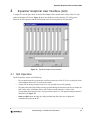
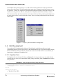
A simple GUI sets the gain values for each of the bandpass filters and the main volume. This GUI runs
under the Windows NT/98 OS. Figure 12 shows the initial state of the equalizer GUI. This section
discusses the GUI operation and the development of this GUI using Microsoft Visual Basic®.
Figure 12. Equalizer Graphical User Interface
4.1 GUI Operation
The GUI interface consists of the following:
•
Eleven equalizer knobs (represented as scroll bars) on the face of the GUI; 10 to set the gain values
of the bandpass filters and 1 to set the main volume.
•
A status line to display messages to the user. It is currently not used for anything
•
Frequency table On/Off checkbox to bring up a small dialog box that allows the user to change the
knob values of the 10 bandpass filters’ gain. When a certain frequency is checked, the
corresponding knob changes to the very top position (a gain of 1). The opposite happens when it is
unchecked (see Figure 13).
•
Setup and Exit buttons to bring up a dialog window that allows the user to change the
communications port on the PC.
Implementing a 10-Band Stereo Equalizer
23
Equalizer Graphical User Interface (GUI)
The bandpass filter gain ranges from 0 to 1, with 0 at the bottom position and 1 at the top. Each knob
allows you to select from 1 of 16 different positions (gain values). Setting the scroll bar to the top causes
the gain to be 1. Hence, the frequencies of that particular band passes through. Setting the scroll bar to the
bottom causes the gain to be 0. Hence, the frequencies of that particular band is removed (or limited).
The main volume knob has 32 positions that can be selected. Sixteen of these positions gradually decrease
the main volume, while 15 increase the main volume. There is one knob position that does not affect the
main volume.
Figure 13. Frequency Table and COM Port Configuration
4.2 GUI Development
The equalizer GUI is implemented in Microsoft Visual Basic®, mainly because this very simple
programming language provides good access to the communications port of a personal computer running
Microsoft Windows. This section briefly describes the code written for the GUI. It is assumed that you
know how to use Microsoft Visual Basic 4.0
4.2.1 Equalizer Form
The Equalizer Form is the main GUI form (see Figure 12). Several procedures are associated with this
form, but only two are key to its functionality: Band_Change() and Send_Data(). Example 11 shows these
two procedures.
Example 11. Baud_Change() and Send_Data() Procedures
Private Sub Band_Change(Index As Integer)
’
BandVal(Index).Caption = Format(31 - Band(Index).Value)
Call Send_Data
End Sub
Private Sub Send_Data()
’ Send Gain info to DSP
If MSComm1.PortOpen Then
24
Implementing a 10-Band Stereo Equalizer
Using the EFCOP in Multichannel Mode
’ First, Send Reset Character
MSComm1.Output = Chr$(13)
For Knob = 0 To 10 Step 1
MSComm1.Output = Chr$((31 - Band(Knob).Value) + 32)
Next Knob
End If
End Sub
The 11 knobs (scroll bars) form an object array element named Band. The Band_Change() procedure is
called when one of the equalizer knobs changes its value. This procedures invokes the Send_Data
procedure, which uses the MSComm1 object to transmit ASCII characters out of the specified
communications port. The value 0x0d is sent out first. Then the position value for each knob is read and
sent out, starting with the 33 Hz knob (see Example 8 on page -13).
4.2.2 Frequency Table Form
Example 12 shows the main procedure for this form.
Example 12. Check1_Click Procedure
Private Sub Check1_Click(Index As Integer)
If Check1(Index).Value = 1 Then
Form1.Band(Index).Value = 0
ElseIf Check1(Index).Value = 0 Then
Form1.Band(Index).Value = 15
End If
End Sub
The 10 checkboxes form an object array element named ‘Check1’. The Check1_Click() procedure changes
the equalizer knob values.
4.2.3 Communications Port Settings Form
The code for the communications port settings form changes the communications port value in the
MSComm1 object.
5
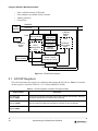
Using the EFCOP in Multichannel Mode
The EFCOP peripheral module functions as a general-purpose, fully programmable filter. It has optimized
modes of operation to perform real and complex impulse response (FIR) filtering, infinite impulse
response (IIR) filtering, adaptive FIR filtering, and multichannel FIR filtering. As Figure 14 shows, the
EFCOP comprises these main functional blocks:
•
Peripheral module bus (PMB) interface, including:
— Data input buffer
— Constant input buffer
— Output buffer
— Filter counter
•
Filter data memory (FDM) bank
Implementing a 10-Band Stereo Equalizer
25
Using the EFCOP in Multichannel Mode
•
Filter coefficient memory (FCM) bank
•
Filter multiplier accumulator (FMAC) machine
•
Address generation
•
Control logic
DMA BUS
PMB
Interface
Control
Logic
GDB BUS
4-Word
FDIR
Data Input Buffer
X Memory
Shared
RAM
Y Memory
Shared
RAM
FCNT
Filter Count
FCM
FCBA
FDM
DATA
Memory Bank
24-bit
Coefficient Base
FDBA
Data Base
Address
Generator
Coefficient
Memory Bank
24-bit
FMAC
24x24 → 56-bit
Rounding & Limiting
FKIR
Filter Constant
Output Buffer
FDOR
Figure 14. EFCOP Block Diagram
5.1 EFCOP Registers
This section documents the registers for configuring and operating the EFCOP (see Table 3). For details
on these registers, consult the DSP56311 User’s Manual (DSP56311UM/D)
Table 3. EFCOP Registers Accessible Through the PMB
Register Name
Description
Filter Data Input
Register (FDIR)
A FIFO four words deep and 24-bits wide for DSP-to-EFCOP data transfers. Data from
the FDIR is transferred to the FDM for filter processing.
Filter Data Output
Register (FDOR)
A 24-bit wide register for EFCOP-to-DSP data transfers. Data is transferred to the FDOR
after processing of all filter taps completes for a specific set of input samples.
Filter K-Constant Input
Register (FKIR)
A 24-bit register for DSP-to-EFCOP constant transfers.
26
Implementing a 10-Band Stereo Equalizer
Using the EFCOP in Multichannel Mode
Table 3. EFCOP Registers Accessible Through the PMB (Continued)
Register Name
Description
Filter Count (FCNT)
Register
A 24-bit register that specifies the number of filter taps. The EFCOP address generation
logic uses the count stored in the FCNT register to generate correct addressing to the
FDM and FCM.
EFCOP Control Status
Register (FCSR)
The DSP56300 core uses this 24-bit read/write register to program the EFCOP and to
examine the status of the EFCOP module.
EFCOP ALU Control
Register (FACR)
The DSP56300 core uses this 24-bit read/write register to program the EFCOP data
ALU operating modes.
EFCOP Data Buffer
Base Address (FDBA)
The DSP56300 core uses this 16-bit read/write register to indicate to the EFCOP the
data buffer base start address pointer in FDM RAM.
EFCOP Coefficient Buffer
Base Address (FCBA)
The DSP56300 core uses this 16-bit read/write register to indicate the EFCOP
coefficient buffer base start address pointer in FCM RAM.
Decimation/
Channel Count
Register (FDCH)
A 24-bit register that sets the number of channels in Multichannel mode and the filter
decimation ratio. The EFCOP address generation logic uses this information to supply
the correct addressing to the FDM and FCM.
5.2 EFCOP Programming for Multichannel Mode
This section discusses how to program the EFCOP to process multiple channels (Multichannel mode) and
shows how the filter coefficients should be set up in memory. EFCOP operation is determined by the
control bits in the FCSR. Multichannel mode is selected by setting FCSR[FMLC]. The number of channels
to process is one plus the number in the FDCH[FCHL] bits. Further filtering operations are enabled via the
appropriate bits in the FACR. After the FCSR is configured, enable the EFCOP by setting FCSR[FEN]. To
ensure proper EFCOP operation, most FCSR bits must not be changed while the EFCOP is enabled.
For each time period, the EFCOP receives the samples for each channel sequentially. This is repeated for
consecutive time periods. Filtering is performed with the same filter or different filters for each channel
using the FCSR[FSCO] bit. If FCSR[FSCO] is set, the same set of coefficients is used for all channels. If
FSCO is clear, the coefficients for each filter are stored sequentially in memory for each channel.
5.2.1 FIR Filter Type
To select the FIR filter type, clear FCSR[FLT]. In single-channel mode, the EFCOP takes an input, x(n),
from the FDIR, saves the input while shifting the previous inputs down in the FDM, multiplies each input
in the FDM by the corresponding coefficient, Bi, stored in the FCM, accumulates the multiplication results,
and places the accumulation result, w(n), in the FDOR. In Multichannel mode, the operation for FIR
filtering is identical but the EFCOP takes the input x(n – 1) instead of x(n). This is done for each sample
input to the FDIR. See Figure 15.
Implementing a 10-Band Stereo Equalizer
27
Using the EFCOP in Multichannel Mode
FDM
FDIR
FCM
x(n-1)
B0
x(n-2)
B1
x(n-3)
B2
x(n-1-N)
BN
FDOR
Figure 15. Multichannel FIR Filter Type Processing
5.2.2 IIR Filter Type
To select the IIR filter type, set the FCSR[FLT] bit. In Single and Multichannel modes, the EFCOP
performs these steps:
1. Multiply each previous output value in the FDM by the corresponding coefficient, A, stored in the
FCM.
2. Accumulate the multiplication results.
3. Add the input, w(n), from the FDIR (which is optionally not scaled by S, depending on the
FACR[FISL] bit setting).
4. Place the accumulation result, y(n), in the FDOR.
5. Save the output while shifting the previous outputs down in the FDM.
This process repeats for each sample input to the FDIR. To process a complete IIR filter, a FIR filter type
session followed by an IIR filter type session is needed.
FDM
FCM
y(n-1)
A0
y(n-2)
A1
y(n-3)
A2
y(n-N)
AN
FDOR
FDIR
Figure 16. Multichannel IIR Filter Type Processing
28
Implementing a 10-Band Stereo Equalizer
Using the EFCOP in Multichannel Mode
5.2.3 Memory Configuration
The EFCOP uses two memory banks:
•
Filter Data Memory (FDM). This 24-bit-wide memory bank is mapped as X memory and stores
input data samples for EFCOP filter processing. The EFCOP Data Base Address (FDBA) register
points to the EFCOP FDM bank.
•
Filter Coefficient Memory (FCM). This 24-bit-wide memory bank is mapped as Y memory and
stores filter coefficients for EFCOP filter processing. The EFCOP Coefficient Base Address
(FCBA) register points to the EFCOP FCM bank.
The number of coefficients, M, used by each channel determines how the filter coefficients and data
samples are stored in FCM and FDM, respectively. The value m = M-1 is stored in the Filter Count
Register (FCNT) to select the number of filter taps that each channel will use. The base address (lower
k
k–1
boundary) value of the FDM and FCM must have zeros in the k LSBs, where 2 ≥ M ≥ 2
. The upper
k
boundary is equal to the lower boundary plus (M –1). Since M ≤ 2 , once M is chosen (that is,
FCNT[11–0] is assigned), a sequential series of data memory blocks (each of length 2k) is created where
k
multiple circular buffers for multichannel filtering can be located. If M < 2 , there is a space between
k
sequential circular buffers of 2 – M (see Figure 17).
The data samples, D(n) are stored in each circular buffer of the FDM starting at the lower addresses. The
EFCOP manages placement of sample data into FDM. The filter coefficients are stored in “reverse order,”
where H(N –1) is stored in each circular buffer of the FCM starting at the lower addresses. These values
must be set up in Y memory before the EFCOP is enabled.
Figure 17 shows an example EFCOP memory configuration. The EFCOP is set in Multichannel mode.
There are two filter channels and each channel has three coefficients. Before the EFCOP is enabled, the
FCM must be initialized. The coefficients for the first channel are stored in reverse order starting from the
FCM base address (0x0). Since each filter has three coefficients (k = 2), the coefficients for the next
channel start at 0x4. After the EFCOP is enabled and initialized, the sample data is sent to the Filter Data
Input Register (FDIR). The EFCOP transfers that data to the FDM. The EFCOP does not touch the 0x3 and
0x7 positions in FDM and FCM.
FCM
FDM
0x0
Channel 1
0x1
0x2
D(0)
0x0
H(2)
D(1)
H(1)
D(2)
H(0)
0x3
0x4
Channel 2
0x5
0x6
D(0)
0x4
H(2)
D(1)
H(1)
D(2)
H(0)
0x7
0x8
0x8
Number of Filter Taps = 3
Figure 17. Memory Configuration Example
Implementing a 10-Band Stereo Equalizer
29
Coefficients and Gain Table Files
6
Coefficients and Gain Table Files
This section lists the coefficients used in both 10-band stereo equalizer implementations. It also lists the
filter and volume gain tables.
Example 13. DSP56311 Core Implementation FIR and IIR Coefficients
;****************************************************************************
;
COEFF.ASM
;
Digital Stereo 10-band Graphic Equalizer Using the 56311
;
;
Copyright (c) MOTOROLA 2000
;
Semiconductor Products Sector
;
Digital Signal Processing Division
;
;******************************************************************************
******************************************************************************
; IIR Coefficients for each of the 10 Bands
;******************************************************************************
31 Hz
DC
.49855285
;beta
DC
.000723575
;alpha
DC
.998544628
;gamma
; 62 Hz
DC
.497109876
DC
.001445062
DC
.997077038
; 125 Hz
DC
.494190149
DC
.002904926
DC
.994057064
; 250 Hz
DC
.488447026
DC
.005776487
DC
.987917799
; 500 Hz
DC
.477154897
DC
.011422552
DC
.975062733
; 1000 Hz
DC
.455306941
DC
.02234653
DC
.947134157
; 2000 Hz
DC
.414266319
DC
.04286684
DC
.88311345
; 4000 Hz
DC
.340894228
DC
.079552886
DC
.728235763
; 8000 Hz
DC
.2601072
DC
.1199464
DC
.3176087
; 16000 Hz
DC
.1800994
DC
.159603
DC
-.4435172
30
Implementing a 10-Band Stereo Equalizer
Coefficients and Gain Table Files
Example 14. EFCOP and DMA Implementation FIR Coefficients
;****************************************************************************
;
FIR_COEFF.ASM
;
Digital Stereo 10-band Graphic Equalizer Using the 56311
;
;
Copyright (c) MOTOROLA 2000
;
Semiconductor Products Sector
;
Digital Signal Processing Division
;
;******************************************************************************
******************************************************************************
; FIR Coefficients for each of the 10 Bands
;******************************************************************************
31 Hz
DC
DC
DC
DC
-.000723575*2
$000000
.000723575*2
$000000
DC
DC
DC
DC
-.001445062*2
$000000
.001445062*2
$000000
DC
DC
DC
DC
-.002904926*2
$000000
.002904926*2
$000000
DC
DC
DC
DC
-.005776487*2
$000000
.005776487*2
$000000
DC
DC
DC
DC
-.011422552*2
$000000
.011422552*2
$000000
DC
DC
DC
DC
-.02234653*2
$000000
.02234653*2
$000000
DC
DC
DC
DC
-.04286684*2
$000000
.04286684*2
$000000
DC
DC
DC
DC
-.079552886*2
$000000
.079552886*2
$000000
DC
DC
DC
-.1199464*2
$000000
.1199464*2
;
;
;
;
A2 = -alpha
A1 = 0
A0 = alpha
Added space to line up Coeffs in memory
; 62 Hz
; 125 Hz
; 250 Hz
; 500 Hz
; 1000 Hz
; 2000 Hz
; 4000 Hz
; 8000 Hz
Implementing a 10-Band Stereo Equalizer
31
Coefficients and Gain Table Files
DC
$000000
DC
DC
DC
DC
-.159603*2
$000000
.159603*2
$000000
; 16000 Hz
Example 15. EFCOP and DMA Implementation IIR Coefficients
;****************************************************************************
;
IIR_COEFF.ASM
;
Digital Stereo 10-band Graphic Equalizer Using the 56311
;
;
Copyright (c) MOTOROLA 2000
;
Semiconductor Products Sector
;
Digital Signal Processing Division
;
;******************************************************************************
******************************************************************************
; IIR Coefficients for each of the 10 Bands
;******************************************************************************
31 Hz
DC
DC
-.49855285/4;B2 = -beta
.998544628/4;B1 = gamma
DC
DC
-.497109876/4
.997077038/4
DC
DC
-.494190149/4
.994057064/4
DC
DC
-.488447026/4
.987917799/4
DC
DC
-.477154897/4
.975062733/4
DC
DC
-.455306941/4
.947134157/4
DC
DC
-.414266319/4
.88311345/4
DC
DC
-.340894228/4
.728235763/4
DC
DC
-.2601072/4
.3176087/4
DC
DC
-.1800994/4
-.4435172/4
; 62 Hz
; 125 Hz
; 250 Hz
; 500 Hz
; 1000 Hz
; 2000 Hz
; 4000 Hz
; 8000 Hz
; 16000 Hz
32
Implementing a 10-Band Stereo Equalizer
Coefficients and Gain Table Files
Example 16. Filter Gain Table
;****************************************************************************
;
Filter_Gain.ASM
;
Digital Stereo 10-band Graphic Equalizer Using the 56311
;
;
Copyright (c) MOTOROLA 2000
;
Semiconductor Products Sector
;
Digital Signal Processing Division
;
;******************************************************************************
******************************************************************************
; Filter Gain (G) Coefficients
;******************************************************************************
DC
DC
DC
DC
DC
DC
DC
DC
-0.200
-0.187
-0.171
-0.160
-0.150
-0.137
-0.114
-0.103
DC
DC
DC
DC
DC
DC
DC
DC
-0.092
-0.080
-0.067
-0.051
-0.039
-0.027
-0.015
0.000
DC
DC
DC
DC
DC
DC
DC
DC
0.000
0.030
0.060
0.090
0.120
0.150
0.180
0.210
DC
DC
DC
DC
DC
DC
DC
DC
0.250
0.290
0.340
0.380
0.460
0.540
0.750
0.999
Implementing a 10-Band Stereo Equalizer
33
Coefficients and Gain Table Files
Example 17. Volume Gain Table
;****************************************************************************
;
Volume_Gain.ASM
;
Digital Stereo 10-band Graphic Equalizer Using the 56311
;
;
Copyright (c) MOTOROLA 2000
;
Semiconductor Products Sector
;
Digital Signal Processing Division
;
;******************************************************************************
******************************************************************************
; Volume Gain (V) Coefficients
;******************************************************************************
34
DC
DC
DC
DC
DC
DC
DC
DC
$1FFB00
$1CE300
$1AD300
$18C300
$16B300
$14A300
$129300
$108300
DC
DC
DC
DC
DC
DC
DC
DC
$0E7300
$0C6300
$0A5300
$084300
$063300
$042300
$021300
$000300
DC
DC
DC
DC
DC
DC
DC
DC
$000000
$110000
$220000
$330000
$440000
$550000
$660000
$770000
DC
DC
DC
DC
DC
DC
DC
DC
$880000
$990000
$AA0000
$BB0000
$CC0000
$DD0000
$EE0000
$FF0000
Implementing a 10-Band Stereo Equalizer
References
7
References
This application note refers to the following resources:
•
DSP56311 User’s Manual, DSP56311UM/D
•
DSP56311 technical data sheet, DSP56303/D
•
Digital Stereo 10-Band Graphic Equalizer Using the DSP56001, APR2/D
•
Programming the CS4218 CODEC for use with DSP56300 Devices, AN1790/D
•
Implementing IIR/FIR Filters with Motorola’s DSP56000/DSP56001, APR7/D, Rev. 2
You can download the Motorola documents from the Web at the following URL:
http://www.mot.com/SPS/DSP
Implementing a 10-Band Stereo Equalizer
35
OnCE, Digital DNA, and the DigitalDNA logo are trademarks of Motorola, Inc.
Motorola reserves the right to make changes without further notice to any products herein. Motorola makes no warranty,
representation or guarantee regarding the suitability of its products for any particular purpose, nor does Motorola assume any liability
arising out of the application or use of any product or circuit, and specifically disclaims any and all liability, including without limitation
consequential or incidental damages. “Typical” parameters which may be provided in Motorola data sheets and/or specifications can
and do vary in different applications and actual performance may vary over time. All operating parameters, including “Typicals” must
be validated for each customer application by customer’s technical experts. Motorola does not convey any license under its patent
rights nor the rights of others. Motorola products are not designed, intended, or authorized for use as components in systems
intended for surgical implant into the body, or other applications intended to support life, or for any other application in which the
failure of the Motorola product could create a situation where personal injury or death may occur. Should Buyer purchase or use
Motorola products for any such unintended or unauthorized application, Buyer shall indemnify and hold Motorola and its officers,
employees, subsidiaries, affiliates, and distributors harmless against all claims, costs, damages, and expenses, and reasonable
attorney fees arising out of, directly or indirectly, any claim of personal injury or death associated with such unintended or
unauthorized use, even if such claim alleges that Motorola was negligent regarding the design or manufacture of the part. Motorola
and
are registered trademarks of Motorola, Inc. Motorola, Inc. is an Equal Opportunity/Affirmative Action Employer.
How to reach us:
USA/EUROPE
Motorola Literature Distribution
P.O. Box 5405
Denver, Colorado 80217
1-303-675-2140
1-800-441-2447
Technical InformationCenter
1-800-521-6274
JAPAN
Motorola Japan Ltd.
SPS, Technical Information Center
3-20-1, Minami-Azabu, Minato-ku
Tokyo 106-8573 Japan
81-3-3440-3569
Home Page
http://www.mot.com/SPS/DSP
DSP Helpline
http://www.motorola-dsp.com/contact
email: [email protected]
ASIA/PACIFIC
Motorola Semiconductors H.K. Ltd.
Silicon Harbour Centre
2 Dai King Street
Tai Po Industrial Estate
Tai Po, N.T., Hong Kong
852-26668334
AN2110/D