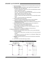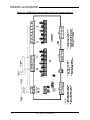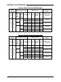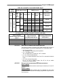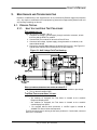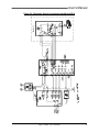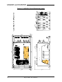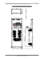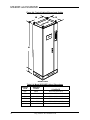
1
Model M3460R Ride-Thru Module (RTM) and Model S3460SR Ride-Thru Cabinet System Customer Reference Manual TEL. (615) 244-2825 ● FAX (615) 244-2833 ● www.bonitron.com Bonitron, Inc. Bonitron, Inc. An Industry Leader in AC Drive Systems and Industrial Electronics OUR COMPANY Bonitron is an international supplier of power controls designed to improve the performance and reliability of electronic systems and variable frequency drives. Located in Nashville, Tennessee, and founded in 1962, Bonitron has gained a reputation for designing and manufacturing products with the highest possible degree of quality and reliability. Bonitron has all the necessary resources in-house for complete electronic product development and manufacturing. Engineering facilities include a CAD lab for circuit board design and engineering labs for prototype testing and evaluation. Production facilities include production areas for circuit board assembly, a machine tool and sheet metal shop for chassis fabrication, and a systems assembly and checkout area. With these assets, Bonitron is positioned to be a leader into the future while maintaining first class support for their current customer base. Worldwide sales of equipment are generated mainly by reputation and referrals. Our customer base includes all of the major drive manufacturers, their distributors, OEMs, end users, and many other satisfied companies. Equipment is installed throughout the United States as well as in Canada, Mexico, Costa Rica, Argentina, Brazil, Chile, Venezuela, Northern Ireland, the Netherlands, Spain, Hungary, Israel, Turkey, China, India, Indonesia, Singapore, Taiwan, and the Philippines. ii Bonitron, Inc. TALENTED PEOPLE MAKING GREAT PRODUCTS The engineering team at Bonitron has the background and expertise needed to design, develop, and manufacture the quality industrial systems demanded by today’s client. A strong academic background supported by continuing education is complemented by many years of hands-on field experience. Expertise encompasses a broad range of applications and engineering solutions such as modern power conversion design techniques and microprocessor-based controls. This insures a solution tailored to the specific needs of the client. A clear advantage that Bonitron has over many competitors is combined on-site engineering labs and manufacturing facilities. This allows the engineering team to have immediate access to and response from testing and manufacturing. This not only saves time during prototype development, but also is essential to providing only the best quality products. AC DRIVE OPTIONS In 1975, Bonitron began working with the AC inverter drive specialists at synthetic fiber plants to develop speed control systems that could be interfaced to their plant process computers. Since that time, Bonitron has developed AC drive option modules that help overcome many of the problems encountered in applications of modern AC variable frequency drives. Bonitron’s Ride-Thru module provides protection from AC line voltage sags while the Line Regen and Resistive Braking modules provide DC Bus regulation for over-voltage due to regenerated voltage. Bonitron AC drive modules are available to provide Undervoltage, Overvoltage, Line Side, Load Side, Maintenance, Power Quality, and Green / Sustainability solutions. These products are compatible with the drives of all major manufacturers and have become the standard in many industries including semiconductor, oil, and fiber. WORLD CLASS PRODUCTS Bonitron has developed over 3000 different modules and systems. Bonitron is willing and able to meet the unique specifications the client may request. Some Bonitron products include: Power Sag Ride-Thru Modules Power Outage Ride-Thru Modules Line Regen Modules Resistive Braking Modules Modular High Speed Precision AC Inverter Systems Inverter Upgrade Modules Multi-motor, Multi-phase Current Sensors Battery Production Charging Systems Data Acquisition Systems Process Controllers Temperature Control Systems RMS True Reading Digital Voltmeters, Ammeters, and Frequency Meters iii M3460R and S3460SR 1. INTRODUCTION ..........................................................................................................................1 1.1. Who Should Use ........................................................................................................................... 1 1.2. Purpose and Scope ........................................................................................................................ 1 1.3. Manual Version ............................................................................................................................ 1 Figure 1-1: Examples of M3460R and S3460SR Ride–Thru Models ...................................................... 1 2. PRODUCT DESCRIPTION ............................................................................................................3 2.1. Features......................................................................................................................................... 3 2.2. Part Number Breakdown .............................................................................................................. 4 Figure 2-1: Example of Part Number Breakdown .................................................................................... 4 Table 2-1: System Voltage Rating Codes ................................................................................................ 4 Table 2-2: Chassis Codes for M3460R Models ....................................................................................... 5 Table 2-3: Cabinet Codes for S3460SR Models ...................................................................................... 5 Table 2-4: Option Codes .......................................................................................................................... 5 2.3. General Specifications .................................................................................................................. 6 Table 2-5: General Specifications Chart .................................................................................................. 6 Table 2-6: Voltage Specifications ........................................................................................................... 6 2.4. General Precautions and Safety Warnings ................................................................................... 7 2.5. Integration Recommendations for Battery Power Source Ride-Thru Systems ............................ 8 3. INSTALLATION INSTRUCTIONS ..................................................................................................9 3.1. Environment ................................................................................................................................. 9 3.2. Unpacking ..................................................................................................................................... 9 3.2.1. Cabinet Units .................................................................................................................................... 9 3.2.2. Open Chassis Units ........................................................................................................................... 9 3.3. Mounting ...................................................................................................................................... 9 3.3.1. Cabinet Units .................................................................................................................................... 9 3.3.2. Open Chassis Units ........................................................................................................................... 9 Figure 3-1: Typical 7.5” Digital Display Panel Mounting Dimensions ................................................. 10 Figure 3-2: Typical 3.6” and 6” Diagnostic Display Panel and Mounting Dimensions ......................... 11 Figure 3-3: Typical 12” Diagnostic Display Panel and Mounting Dimensions ..................................... 11 3.4. Wiring and Customer Connections ............................................................................................. 12 3.4.1. Power Wiring .................................................................................................................................. 12 Table 3-1: Power Field Wiring Connections for Cabinets ..................................................................... 13 Table 3-2: Power Field Wiring Conn for Open Backplates and Cabinets over 125kW ......................... 13 Figure 3-4: Typical Cabinet Field Connections ..................................................................................... 14 Figure 3-5: F39 Cabinet Field Connections ........................................................................................... 14 Figure 3-6: Typical Open Chassis Field Connections with M6 ............................................................. 15 Figure 3-7: Typical Ride-Thru Field Connections with DD3 Display ................................................... 16 Figure 3-8: Recommended Ground Fault Sensing ................................................................................. 17 Figure 3-9: 3460 Power Wiring with Disconnects ................................................................................. 18 Figure 3-10: 3460 Power Wiring from Separate MCC breakers (SCR) ................................................. 19 Figure 3-11: 3460M6 Remote Control and Status Signals ..................................................................... 20 Figure 3-12: Example of Shunt Trip Wiring .......................................................................................... 21 3.4.2. Control Interface Wiring ................................................................................................................. 22 Table 3-3: Cabinet Systems.................................................................................................................... 23 Table 3-4: Open Backplate Modules ...................................................................................................... 23 Table 3-5: Open Backplate Modules with Digital Display .................................................................... 23 Figure 3-13: Basic Fault Contact Wiring to Control Room ................................................................... 23 3.5. Typical Configurations ............................................................................................................... 24 Figure 3-14: 3460R Ride-Thru System Configuration 1 ........................................................................ 24 Figure 3-15: 3460UR Ride-Thru System Configuration 2 ..................................................................... 24 Figure 3-16: 3460R Ride-Thru System Configuration 21 ...................................................................... 25 Figure 3-17: 3460R Ride-Thru System Configuration 23 ...................................................................... 25 iv Table of Contents 4. OPERATION ..............................................................................................................................27 4.1. Functional Description ............................................................................................................... 27 4.2. Features....................................................................................................................................... 28 4.2.1. Indicators / Control Signals for Standard Models ........................................................................... 28 Table 4-1: Control Signal Specifications ............................................................................................... 28 Table 4-2: 3460M6 Control Input Interface I/O Signal Logic Jumper Details....................................... 30 Table 4-3: 3460M6 Status Output Interface I/O Signal Logic Jumper Details ...................................... 30 Figure 4-1: 3660D1 DP Series LED Display ......................................................................................... 31 Figure 4-2: 3660D3 I/O Diagram ........................................................................................................... 31 Figure 4-3: 3460M6 Status Interface Board Layout and Jumper Positions ............................................ 32 Figure 4-4: 3660I Digital Display Board Layout ................................................................................... 33 4.2.2. Displays .......................................................................................................................................... 34 Table 4-4: Diagnostic Display Panel Configurations ............................................................................. 34 Figure 4-5: Display Panels .................................................................................................................... 34 Table 4-5: Manual Control with Enable Signal ...................................................................................... 37 Table 4-6: Manual Control with Disable Signal..................................................................................... 38 Table 4-8: Automatic Control with Enable Signal ................................................................................. 38 Table 4-9: Automatic Control with Disable Signal ................................................................................ 39 4-7: Input Under-Voltage Automatic Shutdown truth table ................................................................... 39 4.3. Startup Procedure ....................................................................................................................... 40 4.3.1. Pre-Power Checks ........................................................................................................................... 40 4.3.2. Startup Procedure and Checks ........................................................................................................ 40 4.4. Threshold Voltage and Low Bus Sense Adjustments ................................................................. 43 Table 4-10: Factory Setpoints for Threshold and Test Boost Voltages.................................................. 44 4.4.1. Determining the Threshold Voltage Setpoint.................................................................................. 44 Figure 4-6: Ride-Thru Module 3460C1 Control Board Layout ............................................................. 46 Figure 4-7: Ride-Thru Module 3460D5 Power Supply Board Layout ................................................... 46 5. MAINTENANCE AND TROUBLESHOOTING ...............................................................................47 5.1. Periodic Testing .......................................................................................................................... 47 5.1.1. Half Voltage Field Test Procedure .................................................................................................. 47 Figure 5-1: Half Voltage Field Test Hook-up ........................................................................................ 47 5.1.2. Periodic Maintenance Procedures for M3460R Without Optional Diagnostic Display Panel ........ 48 5.1.3. Periodic Maintenance Procedures for M3460R With Optional Diagnostic Display Panel ............. 49 5.1.4. Periodic Maintenance Procedures for M3460R With Optional Digital Display Panel ................... 50 5.2. Maintenance Items ...................................................................................................................... 51 5.2.1. Capacitor Replacement Recommendations ..................................................................................... 51 5.3. Troubleshooting .......................................................................................................................... 52 Table 5-1: Troubleshooting Guide ......................................................................................................... 52 Figure 5-2: Diagnostic Signal Connections with M6, I2, and DP17 ...................................................... 54 Figure 5-3: Diagnostic Signal Connections with M6 and DP10 ............................................................ 55 Figure 5-4: Diagnostic Signal Connections with 3534I2 & DP17 ......................................................... 56 Figure 5-5: M3460R Basic Signal Flow with DP** Option ................................................................. 57 Figure 5-6: M3460R Basic Signal Flow with SCR Bridge ................................................................... 58 6. ENGINEERING DATA ................................................................................................................59 6.1. Ratings Charts / Performance Curves ......................................................................................... 59 Table 6-1: 2-second 50% kW Ratings Table.......................................................................................... 59 Table 6-2: Model Specifications ............................................................................................................ 59 6.2. Watt Loss (Inactive Power Consumption) .................................................................................. 60 6.3. Certifications .............................................................................................................................. 60 6.4. Fuse/Circuit Breaker Sizing And Rating .................................................................................... 60 Table 6-3: Input Power Wiring Sizes and Fusing .................................................................................. 60 v M3460R and S3460SR 6.5. Dimensions and Mechanical Drawings ...................................................................................... 61 Figure 6-1: 3460R-R9 Chassis Dimensional Outline ............................................................................. 61 Figure 6-2: 3460R-R10 Chassis Dimensional Outline ........................................................................... 62 Figure 6-3: 3460R-R11 Chassis Dimensional Outline ........................................................................... 63 Figure 6-4: Typical Cabinet Dimensional Outline ................................................................................. 64 Table 6-4: Model S3534SR Cabinet Dimensions .................................................................................. 64 6.6. Recommended Spare Parts ......................................................................................................... 65 Table 6-5: Example of PCB Serial Sticker ............................................................................................. 65 Table 6-6: Spare Parts List ..................................................................................................................... 65 7. APPLICATION NOTES ...............................................................................................................67 7.1. Model M3460R Installation Considerations ............................................................................... 67 7.2. How to Build a High Voltage Ultra Cap Bank ........................................................................... 68 7.3. Diode Sharing with a Bonitron Ride-Thru ................................................................................. 69 Figure 7-1: Ride-Thru System Configuration 19 ................................................................................... 70 Figure 7-2: Diode Sharing With Individual Line Chokes ...................................................................... 70 Figure 7-3: Diode Sharing With Equivalent Drives ............................................................................... 71 Figure 7-4: Typical M3460R Output vs. Input @ Various Loads .......................................................... 71 Figure 7-5: Duration of Voltage Sag in Seconds.................................................................................... 72 Figure 7-6: Typical Drive Bus Voltage for 400VAC Systems (VDC) ................................................... 73 Figure 7-7: Typical Drive Bus Voltage for 460VAC Systems (VDC) ................................................... 74 7.4. Quick Set-up Guide for 3460 Ultra Cap Component Systems ................................................... 75 7.4.1. System wiring ................................................................................................................................. 75 7.4.2. Booster ............................................................................................................................................ 75 7.4.3. Ultra Cap Bank ............................................................................................................................... 75 7.4.4. Blocking Diode ............................................................................................................................... 75 7.4.5. Charger............................................................................................................................................ 75 7.4.6. Charger Isolation Transformer ........................................................................................................ 75 7.4.7. Discharger ....................................................................................................................................... 76 7.5. Quick Set-up Guide for 3460 Electrolytic Cap Component Systems ......................................... 76 7.5.1. System wiring ................................................................................................................................. 76 7.5.2. Booster ............................................................................................................................................ 76 7.5.3. Electrolytic Cap Bank ..................................................................................................................... 77 7.5.4. Blocking Diode ............................................................................................................................... 77 7.5.5. Charging.......................................................................................................................................... 77 7.5.6. Discharger ....................................................................................................................................... 77 vi User’s Manual 1. INTRODUCTION 1.1. WHO SHOULD USE This manual is intended for use by anyone who is responsible for integrating, installing, maintaining, troubleshooting, or using this equipment with any AC drive system. Please keep this manual for future reference. 1.2. PURPOSE AND SCOPE This manual is a user’s guide for the Model S3460SR and M3460R Ride-Thru systems. It will provide the user with the necessary information to successfully install, integrate, and use these in a variable frequency AC drive system. In the event of any conflict between this document and any publication and/or documentation related to the AC drive system, the latter shall have precedence. 1.3. MANUAL VERSION Rev 01b clarifies Digital Display data. Figure 1-1: Examples of M3460R and S3460SR Ride–Thru Models R11 Open Chassis D40 Type-12 Enclosure 1 M3460R and S3460SR This page intentionally left blank 2 User’s Manual 2. PRODUCT DESCRIPTION This document describes the Ride-Thru components used to provide the DC bus power for AC PWM inverter drives during a power line sag or phase loss situation. The Ride-Thru module is factory set to become active (begin supplying power) if the DC bus voltage drops to a preset level. The Ride-Thru module is designed to operate at its rated load for 2 seconds under the following conditions: • A 50% sag in the line voltage on all 3 phases, or • A single-phase loss with the other 2 phases remaining at the rated voltage. The Ride-Thru module’s power rating (kW) must equal that of the drive(s) being supplied by the unit. The Ride-Thru feed should have a 2 second 2x surge capability comparable to the surge rating of the drive(s). The Ride-Thru module is designed to operate continuously, 24 hours per day, 365 days per year. 2.1. FEATURES 1. 2. 3. 4. 5. 6. 7. 8. 9. Easy retrofit installation • Use existing wiring • Use existing feed breakers • Works with most any Fixed bus PWM drive • Only 5 connections (3 to AC line and 2 to drive DC bus) Inexpensive • $100 to $200 per kW • Less expensive than other options • Traditional UPS • Flywheel technology • Capacitive energy storage Easy testing • Can test system “on line” • Can take off line for repair or testing without disrupting the process No maintenance • Ride-Thru time not based on traditional energy storage • Does not degrade after time • Uses less than 100 watts when inactive • No fans or filters for cabinet Ability to add outage backup • Energy storage can be added later using either ultra capacitors or batteries Instant response • No “switchover time” • Maintain control of motor speed and torque Easy commissioning • No programming • Can power up/down with system on-line • Single fine tune level adjustment No RF interference • Slow switching speeds internally filtered • Feeds DC to inverter bus Control Room communications • Single fault contact or complex I/O signals 3 M3460R and S3460SR 10. System monitoring • LEDs • Voltage and current monitoring • Activity counter 11. Over 15 years of on-site experience • Over 1,000 Ride-Thru units installed • Over 10,000 Drives connected • Over 30 companies • Over 10 countries 12. Redundancy • Most models use multiple stages • Single stage failure only means reduced capability 13. Custom options available • Ability to adapt for custom configurations 2.2. PART NUMBER BREAKDOWN Figure 2-1: Example of Part Number Breakdown x3 460 x* H 1 50 R11 DP17, M6, F S BASE MODEL NUMBER SOURCE VOLTAGE RATING KW RATING BACKPLATE OR CABINET CODE ADDED OPTIONS SCR OPTION BASE MODEL NUMBER* The Base Model Number for all Open Chassis Ride-Thru Modules is M3460R. The Base Model Number for all Enclosed Ride-Thru Modules is S3460SR. SOURCE VOLTAGE RATING The Model M3460R Ride-Thru is available in several input voltage ratings. This rating is indicated by a code number as shown in Table 2-1. Table 2-1: System Voltage Rating Codes RATING CODE VOLTAGES (NOMINAL AC LINE / DC BUS) U 115VAC Line / 160VDC L 230VAC Line / 320VDC E 400VAC Line / 565VDC H 460VAC Line / 640VDC C 575VAC Line / 805VDC POWER RATING (KW) The Power Rating indicates the maximum power in kilowatts that can safely be handled by x3460 models and is directly represented by a 3-digit value based on the nominal DC system voltage rating and the maximum output current rating of the RTM. For instance, the rating code for a 150kW RTM is 150. 4 User’s Manual CHASSIS SIZE OR CABINET TYPE The Model M3460R Ride-Thru is available in three open-backplate chassis sizes and the S3460SR is available in several cabinet styles. The size and type is indicated by a code as shown in Tables 2-2 and 2-3. Table 2-2: Chassis Codes for M3460R Models CHASSIS CODE DESCRIPTION R9 34” H x 16” W x 14” D 4-stage open chassis backplate (75-100kW) R10 28” H x 16” W x 14” D 1 or 2-stage open chassis backplate (≤75kW) R11 44” H x 16” W x 14” D 4-stage open chassis backplate (> 100kW) Table 2-3: Cabinet Codes for S3460SR Models CABINET CODE DESCRIPTION D32 42” tall x 37” wide x 16” deep Type-12 wall mount cabinet D33 48” tall x 37” wide x 16” deep Type-12 wall mount cabinet F39 72” tall x 24” wide x 18” deep Type-3-R floor mount cabinet D40 72” tall x 27.5” wide x 18” deep Type -12 floor mount cabinet D50 72” tall x 54” wide x 18” deep Type -12 floor mount cabinet D52 72” tall x 78” wide x 18” deep Type -12 floor mount cabinet CAB1 2000mm tall x 800mm wide x 600mm deep NEMA-12 Hoffman Proline ADDED OPTIONS The Model M3460R Ride-Thru is available with several add-on options if desired. The Added Options are indicated by codes as shown in Table 2-4 and are separated by a comma as shown in Figure 2-1. Option Codes are omitted if not required. Table 2-4: Option Codes OPTION CODE M6 DESCRIPTION Isolated Status Interface D Dual Output K Kinetic Buffering B3 Diagnostic Display Panel (See Section 4.2.2 ) Internal Input AC and Output DC Fusing (Model M3520 External Fuse assemblies also available) Pre-charge hold-off P3 Connections for DC bus bias power supply (for multiple outputs) S SCR Front End Option* DPxx F DD3 Digital Display Notes: • Cabinet Systems include the F and DD3 options. • If the SCR Front End Option is desired, an “S” is added (after a dash “-“) at the end of the part number (See Figure 2-1). • The SCR Front End Option is standard on multi-cabinet systems. 5 M3460R and S3460SR 2.3. GENERAL SPECIFICATIONS Table 2-5: General Specifications Chart SPECIFICATION PARAMETER Output DC Bus Voltage 3-phase, 50/60 Hz (See Table 2-6 below for tolerance and voltage specs) See Table 2-6 below DC Bus Current Rating (Max) See Table 6-1 Power Rating (Max) Boost Circuit Configuration See Table 6-1 Maximum allowed Duty Cycle is: 2 seconds on, 200 seconds off See Section 6.2 50% sag of all 3 phases, duration: 120 cycles (2 sec.), or 100% loss of single phase, duration: 120 cycles (2 sec.) See Table 6-2 DC Bus Threshold See Table 2-6 below Low Bus Fault Setpoint See Table 2-6 below AC Line Input Fusing See Table 6-2 DC Bus Output Fusing See Table 6-2 DC Boost Circuit Fusing See Table 6-2 See Tables 2-2 and 2-3 for styles and sizes of available cabinet mountable open-chassis backplates and cabinets Input AC Line Voltage Duty Cycle (Full Load) Inactive Power Consumption Ride-Thru Requirement Packaging Operating temperature (max.) 40°C Status Output Contacts Opto FET 350VDC @ 120mA Table 2-6: Voltage Specifications AC INPUT TOLERANCE VOLTAGE 6 OUTPUT DC BUS NOMINAL VOLTAGE THRESHOLD VOLTAGE (VDC) LOW DC BUS VOLTAGE FAULT 208 +/- 10% 290 265 (adjustable from 220-300) 230 230 +/- 10% 320 285 (adjustable from 220-300) 250 380 +/- 10% 530 485 (adjustable from 440-540) 450 400 +/- 10% 560 495 (adjustable from 440-540) 460 415 +/- 10% 580 500 (adjustable from 440-540) 465 460 +/- 10% 640 585 (adjustable from 525-625) 550 575 +/- 10% 805 710 (adjustable from 650-750) 675 User’s Manual 2.4. GENERAL PRECAUTIONS AND SAFETY WARNINGS • HIGH VOLTAGES MAY BE PRESENT! • NEVER ATTEMPT TO OPERATE THIS PRODUCT WITH THE ENCLOSURE COVER REMOVED! • NEVER ATTEMPT TO SERVICE THIS PRODUCT WITHOUT FIRST DISCONNECTING POWER TO AND FROM THE UNIT. ALLOW ADEQUATE TIME FOR RESIDUAL • ALWAYS DANGER! VOLTAGES TO DRAIN BEFORE REMOVING THE ENCLOSURE COVER. • FAILURE TO HEED THESE WARNINGS MAY RESULT IN SERIOUS BODILY INJURY OR DEATH! • CERTAIN COMPONENTS WITHIN THIS PRODUCT MAY GENERATE HIGH AMBIENT TEMPERATURES DURING OPERATION. • ALWAYS ALLOW AMPLE TIME FOR THE UNIT TO COOL BEFORE ATTEMPTING SERVICE ON THIS PRODUCT. • BEFORE ATTEMPTING INST ALL ATION OR REMOV AL OF THIS PRODUCT, BE SURE TO REVIEW ALL DRIVE AND/OR CAUTION! RESISTIVE LOAD DOCUMENTATION SAFETY PRECAUTIONS. FOR PERTINENT • INSTALLATION AND/OR REMOVAL OF THIS PRODUCT SHOULD ONLY BE ACCOMPLISHED BY A QUALIFIED NATIONAL ELECTRICIAN IN ACCORDANCE WITH ELECTRICAL CODE OR EQUIVALENT REGULATIONS. • THIS PRODUCT DOES NOT PROVIDE MOTOR OVERLOAD PROTECTION. ANY QUESTIONS AS TO APPLICATION, INSTALLATION, OR SERVICE SAFETY SHOULD BE DIRECTED TO THE EQUIPMENT SUPPLIER. 7 M3460R and S3460SR 2.5. INTEGRATION RECOMMENDATIONS FOR BATTERY POWER SOURCE RIDE-THRU SYSTEMS To protect the booster and battery from damage due to extreme circumstances the booster module should be shut down under the following conditions: • Overtemp • Input Undervoltage • Active run time beyond booster rating FOR STANDARD MODELS OR MODELS EQUIPPED WITH A DP SERIES DISPLAY • The 24V RUN command should be sent through the Input Under Voltage (IUV) and Overtemp (OT) contacts on the 3460M6 interface board. FOR MODELS EQUIPPED WITH DIGITAL DISPLAY (DD3) OPTION • The 24V RUN command should be sent through the Fault 2 contact -OR• The Fault 2 contact should be monitored and the external run command removed when any Fault 2 occurs -OR• The display should be set up for automatic control mode where the display automatically shuts down the enable under any of these conditions. All models should be factory set to automatically shutdown if any of these faults occur. Some end users purposely choose to ignore these warnings because the process is the paramount concern. TO BYPASS THIS SAFETY FEATURE FOR MODELS WITH M6 INTERFACE • Remove series contacts from external run command loop. • Remove factory installed wires between enable input and IUV & OT contacts on 3460M6 board and connect External enable directly to 3460M6 TB7-1 & 2. • Change external run command from Enable to Disable. (Factory set for Enable) • On the 3460M6 interface board move jumpers J15 and J16 from the N.O. position to the N.C. position. The unit will be ready to run automatically upon power up and a 24V command will inhibit boosting. TO BYPASS THIS SAFETY FEATURE FOR MODELS WITH DIGITAL DISPLAY • Change display from automatic to manual mode. • Place display in Manual control mode by ensuring jumper J14 is in the “A” or up position. • Bypass or remove factory installed jumper wire from Fault 2 output. See Section 4.2.4.1. • Change external run command from Enable to Disable. (Factory set for Enable) • On the 3660I2 interface board ensure jumper J15 is in the “B” or down position. The unit will be ready to run automatically upon power up and the external 24V command will inhibit boosting. It is strongly recommended that the safety feature not be bypassed. If it is bypassed it is strongly recommended that the faults be monitored and action be taken immediately upon receiving these faults. 8 User’s Manual 3. INSTALLATION INSTRUCTIONS See Installation Considerations in Section 7. 3.1. ENVIRONMENT The maximum operating temperature of the Ride-Thru system should not exceed 40°C. Non-condensing, filtered air may be required to cool the system. 3.2. UNPACKING 3.2.1. CABINET UNITS 1. Inspect the outer packaging of the Ride-Thru cabinet for shipping damage. • Notify the shipping carrier if damage is found. 2. Remove the banding and outer packaging from the cabinet. • DO NOT remove the hardware securing the cabinet to its pallet! 3. Inspect the Ride-Thru cabinet for shipping damage or loose parts. • Notify the shipping carrier if damage is found. 3.2.2. OPEN CHASSIS UNITS 1. Inspect the M3460R Ride-Thru module crate for shipping damage. 2. Remove screws along bottom of the Ride-Thru module crate, lift cover off. 3. Check all equipment for shipping damage, broken terminals, loose screws, loose or missing IC's, unseated connectors, etc. • Notify the shipping carrier if damage is found. 3.3. MOUNTING 3.3.1. CABINET UNITS 1. Move the cabinet/pallet to the desired installation site. 2. Remove the hardware securing the cabinet to its pallet. 3. Using a crane or hoist connected to the cabinet’s lifting eyes, remove the cabinet from the pallet, and set it in the desired location. • Secure the Ride-Thru cabinet in place. Cabinets may be anchored to the floor as necessary. Cabinets can be top heavy with the doors open! WARNING! 3.3.2. OPEN CHASSIS UNITS The entire Open Chassis Ride-Thru system is mounted on one of three cabinetmountable open-chassis aluminum backplates as follows: • All 2-stage systems rated for up to 127ADC are mounted on the “R10” chassis which measures approximately 28” long by 16” wide by 14” high. • All 4-stage systems rated at 170ADC are mounted on the “R9” chassis which measures approximately 34” long by 16” wide by 14” high. • All 4-stage systems rated for 240ADC or above are mounted on the “R11” chassis which measures approximately 44” long by 16” wide by 14” high. See Figures 6-1 through 6-3. 1. Remove wood screws securing Ride-Thru module backplates to the shipping crate. If a Diagnostic Display panel is not supplied, go to step 5. 9 M3460R and S3460SR 2. Remove the Diagnostic Display panel from the shipping bracket mounted to the Ride-Thru backplate. 3. Unplug wire harness from booster to make display harness installation easier. The Display panel will be installed later. • For DP10 - Disconnect the harness from TB6 of the 3460M6 Status Interface board on the Ride-Thru module. • Figure 3-6 shows the location of the 3460M6 board. • For DP17 - Disconnect the harness from TB2, TB5, and TB7 of the 3534I2 display interface board on the Ride-Thru module. • Figure 3-6 shows the location of the 3534I2 board. • For DD3 - Disconnect the ribbon cable from TB3 of the 3660I DD3 interface board. • Figure 3-7 shows the location of the 3660I2 board. 4. Remove display harness from booster. • Carefully cut cable ties holding display harness to booster backplate. 5. Lift Ride-Thru backplate off of crate bottom using the 4 handles. • If backplate is too heavy, eyebolts may be installed in the mounting holes for lifting by mechanical means. 6. Stand backplate upright in rack and slide the bottom of the backplate into position at the rear of the rack while balancing the top. • See Section 6.5 for Ride-Thru backplate orientation. 7. Secure the Ride-Thru backplate to the rack using the backplate’s .375 inch diameter mounting holes. • See Section 6.5 for Ride-Thru backplate mounting dimensions. If a Diagnostic Display panel is not supplied, go to step 10. 8. Determine where the Diagnostic Display Panel is to be mounted and prepare the site for installation. • The Diagnostic Display Panel is provided with an 8 foot long interconnect harness. • See Figures 3-1 thru 3-3 in this manual for the Diagnostic Display Panel cutout and mounting dimensions. 9. Mount the Diagnostic Display Panel and reconnect the harness to appropriate locations. • See step 3. 10. See Section 3.4 for basic field wiring procedures. Figure 3-1: Typical 7.5” Digital Display Panel Mounting Dimensions DD3 PANEL DIMENSIONS 4X Ø.188 5.000 4.500 CUT-OUT AND FOOTPRINT .250 4X Ø.188 4.500 4.125 .188 .250 7.000 10 7.500 Doc #: 023010 Rev: 20070615 .188 CUTOUT 6.625 7.000 User’s Manual Figure 3-2: Typical 3.6” and 6” Diagnostic Display Panel and Mounting Dimensions DP02 DP10 Figure 3-3: Typical 12” Diagnostic Display Panel and Mounting Dimensions DP17 11 M3460R and S3460SR 3.4. WIRING AND CUSTOMER CONNECTIONS Review this entire Section before attempting to wire the Ride-Thru module. 3.4.1. CAUTION POWER WIRING High voltages supplied to the Ride-Thru include the input AC power and output DC bus. These voltages are derived from different sources. Each source must be separately disconnected and verified zero potential before servicing. Additionally, the Ride-Thru internal DC bus retains a hazardous voltage for several minutes after the input power has been disconnected. Wait at least five minutes after disconnecting power to allow the DC bus to discharge, and then verify zero potential before servicing. Failure to observe these precautions could result in severe bodily injury or loss of life. This section provides information pertaining to the field wiring connections of the M3460R and S3460SR Ride-Thru Cabinet System. Actual connection points and terminal numbers of the AC Drive system will be found in the documentation provided with that system. Be sure to review all pertinent AC Drive System documentation as well as the RTM to Drive Interconnection details listed below before proceeding. 3.4.1.1. SYSTEM WIRING - RTM TO DRIVE INTERCONNECTIONS Several illustrations are provided to assist with the field connection of the 3460 Ride-Thru System to an existing AC drive system. Also, be sure to refer to the documentation supplied with the drive system for field connection points within that system. The DC bus must always be directly connected to the drive output cap bank. Connecting upstream of the DC bus inductors may damage both the drive and the Ride-Thru unit. A typical field connection terminal layout for the S3460SR Cabinet System is shown in Figures 3-4 and 3-5. Additional drawings can be found in Section 6 of this manual. WARNING! Interconnect wiring of this product should only be performed by a qualified electrician in accordance with National Electrical Code or local codes and regulations. 3.4.1.2. TERMINAL LAYOUT 3.4.1.2.1. POWER CONNECTIONS Use copper conductors rated 75°C. See Tables 3-1 and 3-2 for details. GROUND Make ground connection to ground stud located at top of cabinet. AC LINE INPUT CONNECTIONS Make AC line feed connections to appropriately labeled terminals at top of cabinet. (See Figures 3-4 and 3-5) DC BUS OUTPUT CONNECTIONS Make drive DC bus connections to appropriately labeled terminals at top of cabinet. (See Figures 3-4 and 3-5) Always measure DC voltages ensuring that they are at safe levels before making connections. DC BUS INPUT CONNECTIONS 12 User’s Manual Make capacitor bank connections to rectifier bus bars as shown in Figures 3-6 and 3-7. Use hex wrench to hold bolt while loosening nut with an open end wrench. Mount lug through stud onto bus bar. Use Hex wrench to hold bolt while tightening nut. Always measure DC voltages ensuring that they are at safe levels before making connections. Table 3-1: Power Field Wiring Connections for Cabinets TERMINAL TYPE FUNCTION ELECTRICAL MIN WIRE MAX WIRE SPECIFICATIONS AWG AWG TORQUE LB-IN Disconnect Switch AC Input L1, L2, L3 600VAC / x Amps 10 3/0 150 lb-in Disconnect Switch DC Output + ─ 600VAC / x Amps 10 3/0 150 lb-in Limited by Ring Lug Limited by Ring Lug 75 lb-in 10 4/0 150 lb-in Stud (Ring Lug) 3/8” Terminal (Ring Lug) Gnd DC Input + ─ 480VDC / 600 Amps Table 3-2: Power Field Wiring Conn for Open Backplates and Cabinets over 125kW TERMINAL TYPE FUNCTION ELECTRICAL SPECIFICATIONS 3/8” Terminal (Ring Lug) AC Input L1, L2, L3 3/8” Terminal (Ring Lug) Drive Box DC Output + ─ Stud or 3/8” Gnd Terminal (Ring Lug) 3/8” Terminal Cap Bank DC Input (Ring lug on rectifier bus bars) + ─ TORQUE LB-IN MIN WIRE MAX WIRE AWG AWG 1000V / 600 Amps Limited by Ring Lug Limited by Ring Lug 150 lb-in 1000V / 600 Amps Limited by Ring Lug Limited by Ring Lug 150 lb-in Limited by Ring Lug Limited by Ring Lug 75 lb-in Limited by Ring Lug Limited by Ring Lug 75 lb-in 1000V / 600 Amps 13 M3460R and S3460SR Figure 3-4: Typical Cabinet Field Connections 100kW and below DC OUT + ─ POSITIVE NEGATIVE 125kW and above AC LINE INPUT L1 L2 L3 DC BUS (+) (-) (L1) AC LINE (L2) (L3) GND Figure 3-5: F39 Cabinet Field Connections TB2 Shunt Trip Coil Groun AC Line (L3) AC Line (L2) TB1 AC Line (L1) DC Bus (-) DC Bus 14 Dwg #: F39 Field Wiring.jpg Rev: 20060220 AMMETER FIELD POWER WIRING NOTES DC BUS (-) DRIVE AC LINE INPUT (A) AC LINE INPUT (B) AC LINE INPUT (C) GND DRIVE DC BUS (+) REFER TO CUSTOMER REFERENCE MANUAL FOR IMPORTANT INPUT POWER WIRING SIZES AND SOURCE FUSING SELECTION INFORMATION L1 L2 L3 POS. BUS POS. NEG. Dwg #: 090156 Rev: 20101015 NEG. BUS CAPACITOR CONNECTION VOLT METER - THE POSITIONS OF THE CIRCUIT BOARDS SHOWN WILL VARY DEPENDING ON CHASSIS TYPE HOWEVER, THE BOARDS SHOWN ARE USED CONSTANTLY AND TERMINATIONS WILL NOT VARY. 3660D BOARD DP 17 DISPLAY DRIVE 1 3460C1D RIDE-THRU CONTROL BOARD by BONITRON 3460M6B By BONITRON PLC CONNECTIONS + DRIVE 1 SYSTEM MUST HAVE RUN SIGNAL INPUT TO OPERATE TO OPTIONAL DPXX DISPLAY 3460M6B By BONITRON PLC CONNECTIONS SEE SECTION 4 OF CUSTOMER REFERENCE MANUAL FOR DESCRIPTIONS SEE SECTION 5 OF CUSTOMER REFERENCE MANUAL FOR SCHEMATIC User’s Manual Figure 3-6: Typical Open Chassis Field Connections with M6 15 16 DRIVE 1 FIELD POWER WIRING NOTES AC LINE INPUT (B) AC LINE INPUT (C) GND DRIVE DC BUS (-) DRIVE DC BUS (+) REFER TO CUSTOMER REFERENCE MANUAL FOR IMPORTANT INPUT POWER WIRING SIZES AND SOURCE FUSING SELECTION INFORMATION AC LINE INPUT (A) - L1 L2 L3 POS. BUS POS. NEG. Dwg #: 090346 Rev: 20101015 NEG. BUS CAPACITOR CONNECTION + THE POSITIONS OF THE CIRCUIT BOARDS SHOWN WILL VARY DEPENDING ON CHASSIS TYPE HOWEVER, THE BOARDS SHOWN ARE USED CONSTANTLY AND TERMINATIONS WILL NOT VARY. DRIVE 1 SYSTEM MUST HAVE RUN SIGNAL INPUT TO OPERATE 3460C1D RIDE-THRU CONTROL BOARD by BONITRON SEE SECTION 4 OF CUSTOMER REFERENCE MANUAL FOR DESCRIPTIONS SEE SECTION 5 OF CUSTOMER REFERENCE MANUAL FOR SCHEMATIC M3460R and S3460SR Figure 3-7: Typical Ride-Thru Field Connections with DD3 Display User’s Manual Figure 3-8: Recommended Ground Fault Sensing Dwg #: 050163 Rev: 20080723 17 M3460R and S3460SR Figure 3-9: 3460 Power Wiring with Disconnects 18 Dwg #: 010175 Rev: 20070912 User’s Manual Figure 3-10: 3460 Power Wiring from Separate MCC breakers (SCR) Dwg #: 080467 Rev: 20081119 19 M3460R and S3460SR Figure 3-11: 3460M6 Remote Control and Status Signals 20 Dwg #: 080199 Rev: 20090923 Dwg #: 990009 Rev: 20010126 AUX. CONTACT INVERTER POWER OFF ON MDL 1-AMP SLOW BLOW 115V UPS NEUTRAL CONNECT SUCH THAT WHEN THE INVERTER IS SWITCHED OFF, THE RELAY IS DE-ENERGIZED, CONNECTING 115VAC ACROSS THE SHUNT TRIP COIL IN THE BONITRON RIDE-THRU CABINET. WHEN THE SHUNT TRIP COIL IS ENERGIZED, ALL RIDE-THRU POWER IS DISCONNECTED. HOT AC LINE ON MAIN POWER DISCONNECT OFF BONITRON RIDE-THRU CABINET SHUNT TRIP COIL DC BUS 3460 RIDE-THRU CABINET GENERIC SHUNT TRIP COIL WIRING User’s Manual Figure 3-12: Example of Shunt Trip Wiring 21 M3460R and S3460SR 3.4.1.3. SOURCE CONSIDERATIONS Input feed must be capable of delivering 2x rated current for 2 seconds @ 50% sag levels. Feeds sized to account for 150 - 200% inverter starting torque are adequate. * Remember, drive and Ride-Thru will not pull power at the same time. 3.4.1.4. GROUNDING REQUIREMENTS Earth ground stud is provided on backplate. Max torque of 75 in-lbs. 3.4.2. CONTROL INTERFACE WIRING See Figures 3-6 and 3-7 for physical locations. 3.4.2.1. CONTROL CONNECTIONS S3460SR Cabinet systems common control connections are made at TS1 in top section of the cabinet backplate. See Table 3-3 for technical specifications. *Not all control signals are available at this terminal strip. If more detailed status is desired, use directions for connecting to the M3460R booster module. M3460R STANDARD MODELS Booster modules control connections can be made at TB7 on the 3460M6 interface circuit board. See Table 3-4 for technical specifications. See Figure 4-2 for interface board and suggested wiring. M3460R WITH DIGITAL DISPLAY Booster modules control connections can be made at TB1 on the 3660I2 interface board. See Table 3-5 for technical specifications. See Figure 4-2 for interface board and suggested wiring. 3.4.2.2. STATUS MONITORING CONNECTIONS S3460SR Cabinet systems status monitoring connections are made at TS1 in top section of the cabinet backplate. See Table 3-3 for technical specifications. *Not all status signals are available at this terminal strip. If more detailed status is desired, use directions for connecting to the M3460R booster module. M3460R STANDARD MODELS Booster modules systems status monitoring can be made at TB5 on the 3460M6 interface circuit board. See Table 3-4 for technical specifications. See Figure 4-2 for interface board. M3460R WITH DIGITAL DISPLAY Booster modules control connections can be made at TB2 on the 3660I2 interface board. See Table 3-5 for technical specifications. See Figure 4-2 for interface board and suggested wiring. Note 22 For systems using external Ultra Capacitor energy storage AND Digital Display, make cap bank voltage monitoring connection to the 3660I2 interface board as shown in Figure 4-4. User’s Manual Table 3-3: Cabinet Systems Connect to top of cabinet backplate. TERMINAL SIGNAL TYPE FUNCTION TERMINAL # ELECTRICAL SPECS MIN MAX TORQUE WIRE WIRE Sak 2.5 DIS Disable input TS1 20mA @ 24VDC 22 14 4.4 lb-in Sak 2.5 RTA Active output TS1 120mA, 350VDC 22 14 4.4 lb-in Sak 2.5 RTR Ready output TS1 120mA, 350VDC 22 14 4.4 lb-in Sak 2.5 FLT Fault output TS1 120mA, 350VDC 22 14 4.4 lb-in Sak 2.5 AUX Aux output TS1 1A, 460VAC 22 14 4.4 lb-in Table 3-4: Open Backplate Modules Connect to M3460M6 PCB of Booster Module TERMINAL # ELECTRICAL SPECS TB7 20mA @ 24VDC 22 14 2 lb-in TB7 20mA @ 24VDC 22 14 2 lb-in Fault output TB5 & TB6 120mA, 350VDC 22 14 2 lb-in RTR Ready output TB5 & TB6 120mA, 350VDC 22 14 2 lb-in Phoenix Plug RTA TB5 & TB6 120mA, 350VDC 22 14 2 lb-in Phoenix Plug PCC TB5 & TB6 120mA, 350VDC 22 14 2 lb-in Phoenix Plug OT TB5 & TB6 120mA, 350VDC 22 14 2 lb-in Phoenix Plug VF Active output Pre-charge Complete Over Temperature Voltage Fault TB5 & TB6 120mA, 350VDC 22 14 2 lb-in TERMINAL TYPE SIGNAL Phoenix Plug DIS Phoenix Plug TST Enable / Disable input Test input Phoenix Plug FLT Phoenix Plug FUNCTION MIN MAX TORQUE WIRE WIRE Table 3-5: Open Backplate Modules with Digital Display Connect to M3660I2 PCB of Booster Module TERMINAL TYPE SIGNAL Phoenix Plug DIS FUNCTION TERMINAL # ELECTRICAL SPECS TB1 20mA @ 24VDC MIN MAX TORQUE WIRE WIRE Phoenix Plug TST Enable / Disable input Test input TB1 20mA @ 24VDC 22 14 2 lb-in Phoenix Plug FLT 1 Fault 1 output TB2 120mA, 350VDC 22 14 2 lb-in Phoenix Plug FLT 2 TB2 120mA, 350VDC 22 14 2 lb-in Phoenix Plug IUV Fault 2 output Cap bank voltage sensing input TB11 1mA, 1000VDC 22 14 2 lb-in 22 14 2 lb-in Figure 3-13: Basic Fault Contact Wiring to Control Room TO CONTROL ROOM INVERTER FAULT BONITRON RIDE-THRU FAULT Dwg #: 990036 Rev: 20011108 23 M3460R and S3460SR 3.5. TYPICAL CONFIGURATIONS Figure 3-14: 3460R Ride-Thru System Configuration 1 AC LINE DC LINK BOOST REGULATOR 3-PHASE VFD M 2 SECOND, 50% SAG PROTECTION USING DC BOOSTER ONLY FAST DISCHARGE 3 PHASE DC LINK ULTRA 3460 CAP BOOST RESERVOIR REGULATOR AC LINK CHARGER ISOLATION TRANSFORMER Figure 3-15: 3460UR Ride-Thru System Configuration 2 VFD ABOVE 50KW, 0.5 - 2 SECOND, 100% OUTAGE PROTECTION USING DC BOOSTER WITH ULTRA CAP RESERVOIR SINGLE CABINET POWERED FROM AC LINE 24 Dwg #s: 040201 and 040202 Rev: 20080604 M User’s Manual Figure 3-16: 3460R Ride-Thru System Configuration 21 3 PHASE SLAVE SLAVE SLAVE SLAVE SLAVE MASTER CONTROL DC LINK AC LINE SLAVE BOOST REGULATOR VFD M 2 SECOND, 50% SAG PROTECTION USING MULTICABINET DC BOOSTERS Figure 3-17: 3460R Ride-Thru System Configuration 23 3 PHASE 3612 COMMON BUS POWER SUPPLY DC LINK DC INPUT VFD ISOLATION TRANSFORMER DC INPUT VFD DC INPUT VFD 3460R BOOSTER ULTRA CAP RESERVOIR CHARGE REGULATOR MOTOR MOTOR MOTOR CONTINUOUS COMMON DC BUS POWER SUPPLY WITH SHORT TERM 100% OUTAGE PROTECTION USING DC BOOSTER WITH ULTRA CAP RESERVOIR Dwg #s: 070319 and 080224 Rev: 20080604 25 M3460R and S3460SR This page intentionally left blank 26 User’s Manual 4. OPERATION 4.1. FUNCTIONAL DESCRIPTION The M3460R Ride-Thru module consists of three basic sections; the Rectifier section, Boost Converter section, and Control Power Supply. Each of these three sections is described below. RECTIFIER SECTION The Rectifier Section of each slave module converts the 3-phase, AC line to a nominal DC bus. This section contains the input Rectifier Bridge, DC bus filter capacitors, and pre-charge circuitry for standard systems. Upon application of power, the pre-charge circuitry will commence charging the primary bus capacitors through their pre-charge resistors. • For SCR front end systems, upon application of power and a 24V ENABLE command, the 3460B3 pre-charge circuitry will commence charging the primary bus capacitors through their pre-charge resistors. Pre-charge cannot begin unless the ENABLE command is present. Removing the ENABLE command will allow the DC bus to discharge. When the DC bus reaches its proper level, the Boost Converter section will be ready to supply power to the DC bus on demand. When the Boost Converter section is needed, the Pre-charge SCR modules are turned on which provides a path around the pre-charge resistors. BOOST CONVERTER SECTION The Boost Converter Section regulates the DC bus voltage during line sag conditions to a factory pre-set level. Under normal line conditions, the input AC power is fed through resistors around the rectifier SCR modules to the primary filter capacitors. If the AC line voltage sags, the rectifier SCR modules turn on and the Boost Converter section becomes active to regulate the bus voltage. An internal pot establishes this voltage. The voltage is sensed and regulated by the 3460C1 Control Board and pumped up by an IGBT chopper circuit for each stage of the Ride-Thru module. Each chopper circuit includes 1 DC bus inductor, 1 current sensor, and 1 IGBT chopper transistor. If the DC bus level drops, the IGBT chopper transistor is turned on and the DC bus inductor is connected between the primary DC bus and the negative bus. The inductor current increases and energy is stored in the inductor until a maximum current is reached. At this point the transistor is turned OFF and the energy is transferred to the drive DC bus. Each of the DC chopper circuits is phase shifted from the others to minimize peak current demands. The boost chopper will switch as fast as is needed to keep the DC bus at the preset level. When the maximum switching frequency is reached, the DC bus will drop. When the DC bus drops below 400VDC, the run relay will drop out and the bus chopper will stop switching. An over-voltage condition on the DC bus (approximately 750VDC) will cause the Ride-Thru section to shut down. The Ride-Thru Section will be re-enabled once the DC bus voltage drops below approximately 725VDC. If a chopper circuit output fuse should fail, an indicator on its corresponding Blown Fuse Detector will be engaged, and the Ride-Thru Ready signal will turn OFF indicating a fault. The Ride-Thru will continue to operate at a diminished capacity in this fault condition. CONTROL POWER SUPPLY SECTION Control power is derived from the DC bus via the 3460D5 DC-DC power supply board. Voltage for the RUN and TEST contacts is derived from an isolated supply on the 3460D5 board. All control voltages are maintained under all specified sag conditions. 27 M3460R and S3460SR 4.2. FEATURES See Section 2.1 for a synopsis of unit features. 4.2.1. INDICATORS / CONTROL SIGNALS FOR STANDARD MODELS Several control inputs and status outputs are provided for the Ride-Thru system. With the exception of the disconnect status contact, the 3460M6 Status Interface Board receives, monitors, and reports all of the various Ride-Thru system status and control signals. Each of these signals is described in detail here. Table 4-1: Control Signal Specifications CONTROL / STATUS SIGNAL ELECTRICAL RATINGS ACTIVE STATE (AS SET AT FACTORY) Enable Input 24VDC @ 20mA 24VDC to ENABLE and RUN Test Input 24VDC @ 20mA 24VDC to TEST Jumper selectable (see Table 4Ride-Thru Status Outputs Opto-FET, 350VDC@120mA 3 and Figure 4-2) ENABLE INPUT The Ride-Thru may be configured for a 24V ENABLE or DISABLE signal via jumpers J15 and J16. N.O. position means the booster is enabled when 24V is applied; N.C. position means the booster is disabled with 24V applied. The 3460M6 Status Interface board accepts the 24VDC ENABLE / DISABLE signal at TB7-1,2. In order to prevent overheating from constant activity, the OT signal should be used to remove the ENABLE in case the Booster Module overheats. (See Figure 4-2) TEST INPUT The Ride-Thru accepts a normally open momentary contact for TEST and calibration purposes. A TEST button is provided on the DP** Series Diagnostic Display Panels for system testing calibration. This button connects to the system via TB6-10 of the 3460M6 Status Interface board. However, a remote contact can also be connected across terminals TB7-3,4 of the 3460M6 Status Interface board by changing jumpers J10 and J17 to Remote. Closing the TEST contact will cause the Ride-Thru to raise the DC bus level by 100VDC. The inverter input current will drop and the Ride-Thru current will start. If the 3460C1 test time jumper (J4) is set to “EXT”, the DC bus sag setpoint will remain raised for as long as the switch is pressed. If the 3460C1 test time jumper (J4) is set to “INT”, the DC bus sag setpoint will remain raised for 2 seconds. If this is done under load, time-out will occur in 2 seconds. The DPxx series display ‘test’ button may be disabled by placing ASB 3660D jumper J1 in the “B” position. (See Fig. 4-1) This test provides positive proof of Ride-Thru readiness. This test is also useful during field calibration of the Threshold Voltage. (See Section 4.4) STATUS OUTPUTS The 3460M6 Status Interface board provides a pair of output signals (1 local, 1 remote) for each of the individual Ride-Thru status signals as well as for a multiplexed fault output. Each pair of contacts is rated at 350VDC@120mA. All output contacts are jumper selectable for normally open or normally closed conditions to provide proper logic state. Local outputs are provided for display purposes and are routed from the 3460M6, via TB6, to the DP** Series Diagnostic Display panel. Remote outputs are provided for use with a Control Room interface or other control scheme and are routed from the 3460M6, via TB5. Refer to Table 4-3 and Figure 4-2 for details. 28 User’s Manual VOLTAGE FAULT (L-VF & R-VF) The Voltage Fault signal is generated by the 3460X4 Phase Loss Monitor board and passed to the 3460M6 Status Interface board. This contact will OPEN if any single phase of the AC line is missing. This output is provided on the 3460M6 mux board for field connection at TB5-5,6 and for the display panel at TB6-3. OVER TEMPERATURE (L-OT & R-OT) The Over-Temp contact will OPEN if the temperature of any heatsink within the RideThru exceeds 130°F. This output is provided on the 3460M6 mux board for field connection at TB5-3,4 and for the display panel at TB6-4. PRECHARGE COMPLETE (L-PCC & R-PCC) The Precharge Complete contact will CLOSE when the DC bus has reached the preset pre-charge level. This output is provided on the 3460M6 mux board for field connection at TB5-9,10 and for the display panel at TB6-2. RIDE-THRU ACTIVE (L-RTA & R-RTA) The Ride-Thru Active contact will CLOSE if the module is regulating the DC bus voltage under an input voltage sag or TEST condition. The local fault monitor will track Ride-Thru activity in real time for display purposes (if J13 is removed). The remote fault monitor will latch for approximately 3 seconds on Ride-Thru activity to allow adequate time for the fault to read. This output is provided on the 3460M6 mux board for field connection at TB5-11,12 and for the display panel via at TB6-6. RIDE-THRU READY (L-RTR & R-RTR) The Ride-Thru Ready contact will CLOSE when the RUN command is made, precharge is complete and all stage fuses are intact. This output is provided on the 3460M6 mux board for field connection at TB5-1,2 and for the display panel TB6-5. MULTIPLEXED FAULT (L-FAULT & R-FAULT) The Voltage Fault, Over-Temp, and Ride-Thru Ready signals from the system can be combined to provide a pair of multiplexed fault contact outputs. If any of the three multiplexed signals indicates a problem, the Fault output will OPEN after a 3 second delay. This output is provided on the 3460M6 mux board for field connection at TB5-7,8 and for the display panel TB6-1. 29 M3460R and S3460SR Table 4-2: 3460M6 Control Input Interface I/O Signal Logic Jumper Details CONTROL SIGNAL INPUT LOCAL / INPUTS DESIGNATION REMOTE RUN Command Enable Disable N/A Test LOGIC STATE JUMPERS JUMPER N/A J15, J16 Local Remote J10, J17 FACTORY SETTING Normally OPEN (N.O.) Normally CLOSED (N.C.) Local (Loc) Remote (rem) 3460M6 FIELD TERMINALS TB7-1,2 TB7-3,4 Table 4-3: 3460M6 Status Output Interface I/O Signal Logic Jumper Details OUTPUT REMOTE STATUS SIGNAL DESIGNATION Voltage Fault Over Temperature Pre-charge Complete Ride-Thru Active Ride-Thru Ready Multiplexed Fault 30 LOGIC STATE JUMPERS 3460M6 FIELD TERMINALS LOCAL / REMOTE JUMPER FACTORY SETTING L-VF Local J5 Normally CLOSED (N.C.) TB6-3 R-VF Remote J6 Normally OPEN (N.O.) TB5-5,6 L-OT Local J3 Normally CLOSED (N.C.) TB6-4 R-OT Remote J4 Normally OPEN (N.O.) TB5-3,4 L-PCC Local J7 Normally OPEN (N.O.) TB6-2 R-PCC Remote J8 Normally OPEN (N.O.) TB5-9,10 L-RTA Local J13 Normally OPEN (N.O.) TB6-6 R-RTA Remote J14 Normally OPEN (N.O.) TB5-11,12 L-RTR Local J1 Normally OPEN (N.O.) TB6-5 R-RTR Remote J2 Normally OPEN (N.O.) TB5-1,2 L-FAULT Local none Normally CLOSED (N.C.) TB6-1 R-FAULT Remote J10 Normally OPEN (N.O.) TB5-7,8 User’s Manual Figure 4-1: 3660D1 DP Series LED Display Test Switch Test Jumper 3660D1C by BONITRON Figure 4-2: 3660D3 I/O Diagram 31 M3460R and S3460SR Figure 4-3: 3460M6 Status Interface Board Layout and Jumper Positions 32 Dwg #: 090187 Rev:20090923 User’s Manual Figure 4-4: 3660I Digital Display Board Layout Dwg #: 100031 Rev: 20101014 33 M3460R and S3460SR 4.2.2. DISPLAYS DIAGNOSTIC DISPLAY PANEL (OPTIONAL) 4.2.2.1. The Ride-Thru Diagnostic Display Panel provides visual indication of the RideThru module’s operating status and also permits a system test to be performed. Currently, there are several display panel configurations available with various combinations of features as detailed in Table 4-4 and Figure 4-5. Table 4-4: Diagnostic Display Panel Configurations COUNTERS METERS PANEL LEDS & TEST NUMBER SWITCH VOLTMETER AMMETER DP2 9 DP10 9 DP17 9 9 9 DD3 9 9 9 ACTIVE CYCLES TOTAL CYCLES 5” x 3.6” 9 5” x 6” 9 9 5” x 12” 9 9 7.5” x 5” Figure 4-5: Display Panels DP02 DP10 POWER POWER PRECHARGE COMPLETE PRECHARGE COMPLETE RIDETHRU READY RIDETHRU READY RIDETHRU ACTIVE RIDETHRU ACTIVE ACTIVE CYCLES VOLTAGE FAULT VOLTAGE FAULT OVER TEMP TEST SYSTEM OVERTEMP TEST SYSTEM DP17 DD3 BUS CURRENT BUS VOLTAGE POWER PRECHARGE COMPLETE RIDETHRU READY TOTAL RTA CYCLES RIDETHRU ACTIVE VOLTAGE FAULT OVERTEMP ACTIVE CYCLES TEST 34 PANEL DIMS. User’s Manual 4.2.2.1.1. SYSTEM LED STATUS DISPLAY BOARD FOR ALL DPXX DISPLAYS The System Status Display module provides visual indication of various system functions. The monitored functions include POWER, PRECHARGE COMPLETE, RIDE-THRU READY, RIDE-THRU ACTIVE, VOLTAGE FAULT, and OVERTEMP. In addition, this module provides the system TEST switch required for threshold voltage adjustments and system calibration. The functions of each of these indicators are described below. POWER LED The green Power LED is ON if power is applied to the system. (PCC) PRECHARGE COMPLETE LED The green Precharge Complete LED is ON if the DC bus has reached the factory preset pre-charge level. (RTR) RIDE-THRU READY LED The green Ride-Thru Ready LED is ON if the module is fully operational and capable of regulating the rated DC bus voltage under the specified power sag conditions. (RTA) RIDE-THRU ACTIVE LED The amber Ride-Thru Active LED is ON if the module is regulating the DC bus voltage under an input line sag condition. VOLTAGE FAULT LED The red Voltage Fault LED is ON if any single phase of the AC line input is missing. OVER TEMPERATURE LED The red Overtemp LED is ON if the backplate temperature exceeds 130°F. TEST SYSTEM SWITCH The Test System push-button switch will cause the Ride-Thru section to raise the DC bus sag setpoint by approximately 100VDC (see Table 4-9). The inverter input current will drop and the Ride-Thru current will start. If the 3460C1 test time jumper (J4) is set to “EXT”, the DC bus sag setpoint will remain raised for as long as the switch is pressed. If the 3460C1 test time jumper (J4) is set to “INT”, the DC bus sag setpoint will remain raised for 2 seconds. If this is done under load, time-out will occur in 2 seconds. The DPxx series display ‘test’ button may be disabled by placing ASB 3660D jumper J1 in the “B” position. This test provides definite proof of Ride-Thru readiness and is also useful during field calibration of the Threshold Voltage. 4.2.2.1.2. AVAILABLE INDICATIONS FOR ALL DPXX DISPLAYS BUS VOLTAGE METER (DP17, DP11) The Bus Voltage meter indicates the Ride-Thru DC bus voltage. The voltmeter is driven from the 3534I2 board. The 3534I2 board uses a voltage divider connected across the DC bus to drive the panel meter with 300k ohm impedance between the meter and each ± bus. The Voltmeter will read slightly lower than the drive bus when idle. BUS CURRENT METER (DP17) The Bus Current meter indicates the positive DC bus current supplied by the Ride-Thru module. The current is sensed by an isolated Hall Effect device and the meter is driven from the 3534I2 board. ACTIVE CYCLES COUNTER (DP10, DP11, DP17) The Active Cycles Counter indicates the number of times the Ride-Thru module has been active since this counter was last reset. The counter is battery powered and therefore does not lose its count during a power 35 M3460R and S3460SR outage. The counter may be reset to zero by pressing the Reset pushbutton. This button is located to the right on the front face of the counter. TOTAL RTA CYCLES COUNTER (DP17) The Total RTA Cycles Counter indicates the lifetime total number of times the Ride-Thru module has been active. The counter is battery powered and therefore does not lose its count during a power outage. This counter is not affected by the Reset push-button located to the right on the front face of the counter. 4.2.2.2. BASIC DD3 DISPLAY SET UP FOR 3460 BOOST MODULES 4.2.2.2.1. INPUT COMMANDS ENABLE MODE In this mode an external 24V input command causes the booster to become enabled providing there are no fault conditions. A fault condition may shut down the run command to the booster depending on the position of J1 and J14 and the DD3 display setting. DISABLE MODE In this mode the booster will become automatically enabled once powered up and all conditions are met. An external 24V input command causes the booster to become disabled, and no boosting can occur. Use this mode if no external run command is used. To make external input an enable command place J15 in the “A” position. To make external input a disable command place J15 in the “B” position. TEST MODE In this mode a 24V input will cause the booster output voltage to increase so that the drive rectifier is reversed biased and power will flow from booster, proving switching circuits are operational and fuses are intact. Test can be initiated by an external contact or from the DD3 display panel. To Enable test mode place J11 “ON” (connecting both pins) To Disable test mode place J11 “OFF” (on one pin only) 4.2.2.2.2. CONTROL MODES AUTOMATIC In this mode the processor monitors temperature, active run time, and input voltage, and can shut down the boost function if these go outside of desired parameters. These conditions generate a Fault signal (fault 2) and are available for remote notification. The Input under-voltage (IUV) meant to protect the battery bank from deep discharge can be disabled from the front panel in cases where process is more important than battery life. MANUAL CONTROL MODE In this mode the processor will only monitor the system status, and will not shut down the run command. In this mode It is recommended that fault signals are monitored, and a remote enable or disable signal be used to stop the switching. *In the effort of keeping the Bonitron module from running outside its specifications, Bonitron will ship with the system set up for automatic control. Since some applications are of such crucial importance, we realize the desire to continue running may outweigh any concerns for the Ride Thru modules or battery bank. If your application is this critical, you may want to use the manual mode. 36 User’s Manual To place the display in the Manual mode so that automatic shutdown does NOT occur, place J1 and J14 in the “A” positions. To place the display in the Automatic mode, place J1 and J14 in the “B” positions. 4.2.2.2.3. OUTPUT STATUS SIGNALS FAULT 1 Fault 1 will change states if OUV or BF occur, or if RTR & PCC turn off, signaling to the control room that an operator should go out and check the Ride Thru front panel for more information. This signal may be considered a “READY” signal. Both N.O. and N.C. contacts are available at the connector. FAULT 2 OUTPUT Fault 2 will change states only if Over-Temp, Input Under-Voltage, or Active Time faults occur. If any of these faults occur, and the Ride Thru is in automatic control, the run command will be shut down. If fault 2 occurs, and the display is in manual mode, there should be immediate attention given to the Ride Thru system, and remotely shutting down the boost function should be considered. Both N.O. and N.C. contacts are available at the connector. Table 4-5: Manual Control with Enable Signal 3660I JUMPERS J1 J14 J15 3660I SIGNAL INPUTS OT, IUV OR RTO RTR, PCC, BF A or “ENABLE” ENABLE FLT 1 FLT 2 OR RUN 1 & LATCH RUN 2 DISPLAY FAULT INDICATIONS OUV OK A or “MANUAL” 3660D DISPLAY PANEL 3660I OUTPUTS Fault OK Fault 24V - - X - 0 - - - - 24V - X X Y 0 - X - Y 24V - - X N 0 - - - N 24V X - X N 0 X - - N Normal Temp, Batt UV or RTA Time Normal RTR, PCC, BF or OUV 37 M3460R and S3460SR Table 4-6: Manual Control with Disable Signal 3660I JUMPERS J1 J14 J15 3660I SIGNAL INPUTS OT, IUV OR RTO RTR, PCC, BF B or “DISABLE” ENABLE FLT 1 FLT 2 OR RUN 1 & LATCH RUN 2 DISPLAY FAULT INDICATIONS OUV OK A or “MANUAL” 3660D DISPLAY PANEL 3660I OUTPUTS Fault OK Fault 24V - - - - 0 - - X - 24V - X - Y 0 - X X Y 24V - - - N 0 - - X N 24V X - - N 0 X - X N Normal Temp, Batt UV or RTA Time Normal RTR, PCC, BF or OUV Table 4-7: Automatic Control with Enable Signal 3660I JUMPERS J1 J14 J15 3660I SIGNAL INPUTS OT, IUV OR OR Fault OK Fault 38 ENABLE FLT 1 FLT 2 RUN 1 & LATCH RUN 2 DISPLAY FAULT INDICATIONS OUV OK A or “ENABLE” B or “AUTOMATIC” RTO RTR, PCC, BF 3660D DISPLAY PANEL 3660I OUTPUTS 24V - - X - 0 - - - - 24V - X - Y 0 - X - Y 24V - - X N 0 - - - N 24V X - X N 0 X - - N Normal Temp, Batt UV or RTA Time Normal RTR, PCC, BF or OUV User’s Manual Table 4-8: Automatic Control with Disable Signal 3660I JUMPERS J1 J14 3660I SIGNAL INPUTS J15 OT, IUV OR ENABLE FLT 1 FLT 2 OR RUN 1 & LATCH RUN 2 DISPLAY FAULT INDICATIONS OUV OK B or “DISABLE” B or “AUTOMATIC” RTO RTR, PCC, BF 3660D DISPLAY PANEL 3660I OUTPUTS Fault OK Fault 24V - - - - 0 - - X - 24V - X - Y 0 - X - Y 24V - - - N 0 - - X N 24V X - - N 0 X - X N Normal Temp, Batt UV or RTA Time Normal RTR, PCC, BF or OUV 4-9: Input Under-Voltage Automatic Shutdown truth table DISPLAY SCREEN “DISABLE RIDE-THRU FOR IUV FAULT” J1 & J14 POSITION ON 3660I INTERFACE PCB AUTOMATIC SHUTDOWN ON IUV FAULT No No Yes Yes Pos “A” (Manual) Pos “B” (Auto) Pos ”A” (Manual) Pos “B” (Auto) No No No Yes 4.2.2.2.4. DD3 DISPLAY JUMPER POSITION DESCRIPTIONS The following jumpers are located on the 3660I interface pcb mounted on the boost module, connected to display panel via 16 pin ribbon cable. • J2 = Program enable. “Off” to program, “On” during normal operation • J11 = Test Mode enable “On” to enable local or remote test, “OFF” to disable • J1, J14 = Control mode selection Pos “A” for manual shutdown mode, Pos “B” for automatic shutdown mode • J15 = Run command logic state Pos “A” for 24V to enable booster, Pos “B” for 0V (no enable connection) to enable booster 4.2.2.2.5. FACTORY SET UP WHEN USING DD3 DISPLAY MODULE RUN COMMAND Factory set for operation without external input command (J15 in the “B” position). CONTROL MODE Factory set for automatic shutdown with IUV disabled from front panel (J1 and J14 in the “B” position and display programmed to ignore IUV for auto-shutdown). 39 M3460R and S3460SR 4.3. STARTUP PROCEDURE 4.3.1. PRE-POWER CHECKS 1. Ensure the Bonitron Ride-Thru has been properly installed as per the instructions in Section 3 of this manual. 2. The Ride-Thru DC bus threshold must be coordinated with the under voltage trip setting of the inverter. If the threshold is too close to the nominal bus, the Ride-Thru may supply power to the drive continuously, and overheat. If the threshold is too close to the under voltage trip level of the inverter, the system may not "Ride-Thru", and under voltage trips will still occur. Most inverters have an under voltage trip point of -15% of nominal. Some inverters can be reprogrammed to change this trip level. Bonitron typically would like the DC bus threshold to be about -10% of the nominal bus. For example, Bonitron sets all 460VAC systems to hold the DC bus to 585VDC. • Refer to your inverter's documentation for details on adjustment of the under voltage trip setting. • Refer to Section 4.4 for details on how the Ride-Thru DC bus threshold can be changed. 3. If equipped with the Ride-Thru disconnect, turn off, and apply power to the system. Otherwise, go to the Startup Procedure Section 4.3.2.1. • Ensure that the associated inverter is working properly. • Confirm the under voltage trip point if possible. 4. Ensure that the associated inverter is working properly. • Confirm the under voltage trip point if possible. 4.3.2. STARTUP PROCEDURE AND CHECKS 4.3.2.1. CAUTION! FOR M3460R WITHOUT DIAGNOSTIC DISPLAY PANEL If Precharge Hold-off “B3” option is installed, begin with step 1. installed, go directly to step 2. If not 1. If this unit HAS the Precharge Option installed: Apply power to the RideThru and observe the following conditions: • DC bus voltage on Ride-Thru cap bank does not charge. • No LEDs should light. • Turn on the 24V ENABLE signal and observe the following conditions: • DC bus voltage on Ride-Thru cap bank should quickly rise to the nominal system bus voltage. • 3460C1 control board LED 6 (+15V) should be ON. • 3460C1 control board LED 7 (-15V) should be ON. • 3460C1 control board LED 4 (PCC) should be ON. • 3460C1 control board LED 3 (RTR) should be ON. • All other 3460C1 LEDs should be OFF. • 3460M6 fault output board LED (No Fault) should be ON. • Skip step 2 2. If this unit DOES NOT HAVE the Precharge Option installed: Apply power to the Ride-Thru and observe the following conditions: • DC bus voltage on the Ride-Thru cap bank should rise quickly to the nominal system bus voltage. • 3460C1 Control board LED 6 (+ 15V) should be ON. • 3460C1 Control board LED 7 (− 15V) should be ON. • 3460C1 Control board LED 4 (PCC) should be ON. 40 User’s Manual • 3460C1 Control board LED 3 (RTR) should be ON. • All other 3460C1 LEDs should be OFF. • 3460M6 Fault Output board LED 1 (No Fault) should be ON. 3. Verify Control Room Connections (if used). Control Room should read the Ride-Thru status signals as found in the Section 4.2. • Move jumper positions on 3460M6 to simulate signals • See Figure 3-11 for connection details. 4. Verify threshold setpoint. • Turn off system power and watch the DC bus voltage fall. Refer to the Threshold Adjustment procedure in Section 4.4. • 3460C1 Control board LED 2 (RTA) will come ON when the bus drops to the threshold. • The DC bus will hold at the threshold momentarily. • Allow the DC bus to discharge until the 3460C1 Control board LED 4 (PCC) goes OFF. • Reapply system power. 5. Verify system capability. Monitor DC bus voltage and DC bus current, or inverter AC line current. • Input 24V TEST signal on 3460M6 TB7-3&4. (See Threshold Adjustment Procedure, Section 4.4). • 3460C1 Control Board LED 2 (RTA) should come ON during test (RTA will flash if the load is light, stay on if the load is heavy). • 3460C1 Control Board LED 1 (TEST) should come ON during test. • Bonitron DC bus voltage should rise to the test boost level. • Inverter DC bus should rise to the test boost level. • Motor should not lose speed or torque. • DC bus current should flow from Ride-Thru to inverter. • Inverter input current should decrease. This completes the startup procedure for M3460R without the Diagnostic Display Panel. 4.3.2.2. CAUTION! FOR M3460R WITH DP17 DIAGNOSTIC DISPLAY PANEL If Precharge Hold-off “B3” option is installed, begin with step 1. If not installed, go directly to step 2. 1. If this unit HAS the Precharge Option installed: Apply power to the RideThru and observe the following conditions: • DC bus voltage on Ride-Thru cap bank does not charge. • No LEDs should light. • Turn on the 24V ENABLE signal and observe the following conditions: • DC bus voltage on Ride-Thru cap bank should quickly rise to the nominal system bus voltage. • DC bus current should remain at zero. • Power LED should be ON. • Precharge Complete LED should be ON. • Ride-Thru Ready LED should be ON. • Ride-Thru Active LED should be OFF. • Voltage Fault LED should be OFF. • Overtemp LED should be OFF. • 3460M6 fault output board LED (NO fault) should be ON. • Skip step 2 Doc #: 013012 Rev: 20030128 41 M3460R and S3460SR 2. If this unit does NOT have the Precharge Option installed: Apply power to the Ride-Thru and observe the following conditions on the DP17 Display panel: • Power LED should be ON. • Precharge Complete LED should be ON. • Ride-Thru Ready LED should be ON. • Ride-Thru Active LED should be OFF. • Voltage Fault LED should be OFF. • Overtemp LED should be OFF. • The Bus Current Meter should read 0 amps. • The Bus Voltage Meter should read NOMINAL DC bus voltage. 3. Verify Control Room Connections (if used). Control Room should read the Ride-Thru status signals as found in the Section 4.2. • Move jumper positions on 3460M6 to simulate signals. • See Figure 3-11 for connection details. 4. Verify threshold setpoint. • Turn off system power and watch the DC bus voltage fall. Refer to the Threshold Adjustment procedure in Section 4.4. • RIDE-THRU ACTIVE LED will come ON when the bus drops to the threshold. • The DC bus will hold at the threshold momentarily. • Allow the DC bus to discharge until the PCC LED on the display panel goes OFF. • Reapply system power. 5. Verify system capability. Monitor DC bus voltage and DC bus current, or inverter AC line current. • Initiate the Test sequence. (See Threshold Adjustment Procedure in Section 4.4) • RIDE-THRU ACTIVE LED on DP17 Display should come ON during test (RTA will flash if the load is light, stay on if the load is heavy). • 3460C1 Control Board LED 1 (TEST) should come ON during test. • Bonitron DC bus voltage should rise to the test boost level. • Inverter DC bus should rise to the test boost level. • Motor should not lose speed or torque. • DC bus current should flow from Ride-Thru to inverter. • Inverter input current should decrease. This completes the startup procedure for M3460R with Diagnostic Display Panel. 4.3.2.3. CAUTION! FOR M3460R WITH DD3 DIGITAL DISPLAY PANEL If Precharge Hold-off “B3” option is installed, begin with step 1. If not installed, go directly to step 2. 1. If this unit HAS the Precharge Hold-off Option installed: Apply power to the Ride-Thru and observe the following conditions: • No LEDs should light. • Turn on the 24V ENABLE signal and observe the following conditions: • DC bus voltage on Ride-Thru cap bank should pre-charge to the nominal system bus voltage. • DC bus current should remain at zero. • Power LED should be ON. 42 Doc #: 013012 Rev: 20030128 User’s Manual • Ride-Thru Active LED should be OFF. • Voltage Fault LED should be OFF. • Skip step 2 2. If this unit DOES NOT HAVE the Precharge Hold-off Option installed: Apply power to the Ride-Thru and observe the following conditions on the Digital Display panel: • Power LED should be ON. • Ride-Thru Active LED should be OFF. • Voltage Fault LED should be OFF. • The Bus Current Meters should read 0 amps. • The Bus Voltage Meters should read NOMINAL DC Bus voltage with Input slightly higher than Output. 3. Verify Control Room Connections (if used). Control Room should read the Ride-Thru Fault 1 and Fault 2 signals as found in the Section 4.2. • Unplug 3660I connector and insert jumper into plug end to simulate fault • See Figure 4-3 for connection details. 4. Verify threshold setpoint. • Turn off system power and watch the DC bus voltage fall. Refer to the Threshold Adjustment procedure in Section 4.4. • Ride-Thru Active LED will come ON when the bus drops to the threshold. • The DC bus will hold at the threshold momentarily. • Allow the DC bus to discharge until the PCC LED on the display panel goes OFF. • Reapply system power. 5. Verify system capability. Monitor DC bus voltage and DC bus current, or inverter AC line current. • Initiate the Test sequence. (See Digital Display manual to navigate to the test screen) • Ride-Thru Active LED on Digital Display should come ON during test. • 3460C1 Control Board LED 1 (TEST) should come ON during test. • Bonitron DC bus voltage should rise to the test boost level. • Inverter DC bus should rise to the test boost level. • Motor should not lose speed or torque. • DC bus current should flow from Ride-Thru to inverter. • Inverter input current should decrease. This completes the startup procedure for M3460R with Digital Display Panel. 4.4. THRESHOLD VOLTAGE AND LOW BUS SENSE ADJUSTMENTS OVERVIEW The "Threshold" voltage level is the voltage at which the Bonitron Model M3460 Ride-Thru module maintains the DC bus during a power sag. Whenever the DC bus level drops to the "Threshold" setpoint, the Ride-Thru module becomes active to regulate the DC bus voltage to the "Threshold" setpoint voltage. Generally, the “Threshold” level should be set at 10-15% below the nominal DC bus level. An actual on-site level setting must be determined by the loaded DC bus level as well as the amount of ripple present on the DC bus. The Ride-Thru module should not become active during normal everyday operation. The "Threshold" level is factory preset on all Bonitron Model M3460 Ride-Thru modules. These levels are specified in the General Specifications Chart in Section 2 of this manual for each Ride-Thru module. However, some field adjustment of this level may be required to achieve the optimum setpoint level for any given system. Doc #: 013012 Rev: 20030128 43 M3460R and S3460SR It is important to note that the Ride-Thru module’s "Low DC Bus" or "Output Under-Voltage (OUV)" or “Kinetic Buffering” (KB) setpoint is factory preset to 5% below the "Threshold" voltage, whichever is greater. This setpoint should be a minimum of 25V below Threshold to avoid improper OUV fault activity. *** Please note that not all models are wired to utilize the Output Under-Voltage fault. *** Table 4-9 below lists the typical factory setpoints for the "Threshold", "Low DC Bus (OUV)" and "Test Boost" levels for the Model M3460 Ride-Thru modules based on the system AC or DC input voltage requirements. Be sure to check this manual for each Ride-Thru module for specific setpoint levels. Table 4-10: Factory Setpoints for Threshold and Test Boost Voltages NOMINAL INPUT VOLTAGE MINIMUM INPUT VOLTAGE THRESHOLD LOW DC BUS (OUV) (KB) TEST BOOST 230VAC line 115VAC 285VDC 260VDC +50VDC 380VAC line 190VAC 485VDC 450VDC +100VDC 400VAC line 200VAC 495VDC 460VDC +100VDC 415VAC line 208VAC 500VDC 465VDC +100VDC 460VAC line 230VAC 585VDC 550VDC +100VDC 575VAC line 287VAC 710VDC 675VDC +125VDC 4.4.1. DETERMINING THE THRESHOLD VOLTAGE SETPOINT Testing and adjustment of the "Threshold" voltage setpoint can be performed on systems in either an "On-line and loaded" or an "Off-line and unloaded” condition as described in methods 1 and 2 below. Each of the two methods described require that you monitor the DC bus voltage during the testing and adjustment procedures. Be sure to read through both adjustment methods completely before attempting any adjustment of the "Threshold" and "Low DC Bus" voltage setpoints. METHOD 1: DETERMINING THE THRESHOLD VOLTAGE SETPOINT FOR AN ON-LINE AND LOADED SYSTEM 1. Verify proper installation. • Ensure that the Bonitron Model M3460 Ride-Thru module has been properly installed and wired according to all applicable system and module wiring diagrams. 2. Initiate the “test” sequence while monitoring the DC bus voltage. • On modules so equipped, the "Test" button is located on the module's control/display front panel. (For modules without a control/display front panel, a +24VDC signal is needed at 3460M6 TB7-3&4 to initiate “test” sequence). 3. Read the DC bus meter and subtract the "Boost" voltage. • When the "Test" is initiated, the "Threshold" voltage level is "Boosted" for a certain period of time. This time interval is dependent upon the setting of jumper J4 on the 3460C1 Control Board. With the J4 jumper in the INT position, the interval will be approximately 2 seconds. With the jumper in the EXT position, the Boost will be maintained in real-time by the Test for as long as the Test is performed. • During this "Boost" period, you should see the DC bus level increase. The amount that the DC Bus actually increases will depend on the Boost and 44 User’s Manual Threshold level adjustments as well as the input voltage and DC bus output current. • For example, for a Ride-Thru system with an input voltage of 460VAC, the "Threshold" voltage level is preset to be 585VDC and the "Boost" voltage level is factory preset for an increase of 100VDC. • Assuming that these preset levels have not been altered, initiating the test described above on a lightly loaded system of this nature would cause the DC bus level to rise to 685VDC (585VDC + 100VDC). Subtracting the "Boost" voltage (100VDC) from this reading shows that the actual "Threshold" voltage level is 585VDC. • Initiating this test on a heavily loaded system of this nature would also cause the DC bus level to rise. However, the DC bus would stop rising once current limit is reached. NOTE: The "Boost" voltage level is adjustable and is factory preset. It is not recommended that this setpoint be altered. If this setpoint has been changed from its original factory setting, this test method will not be accurate. METHOD 2: DETERMINING THE THRESHOLD VOLTAGE SETPOINT FOR AN OFF-LINE AND UNLOADED SYSTEM 1. Remove input voltage supply from system. • Disconnect the input voltage to the Ride-Thru while monitoring the DC bus voltage. • As the DC bus drops to the "Threshold" setpoint voltage, the Ride-Thru module will become active. • The Ride-Thru will then maintain the DC bus voltage at the "Threshold" setpoint level for approximately 1 second while the primary capacitor discharges, at which point, the DC bus will continue to drop. • Read the DC bus voltage as it is being maintained. This is the "Threshold" setpoint voltage. ADJUST THE SETPOINTS AND REPEAT THE TEST Once the actual "Threshold" voltage has been determined you can make adjustments, if required, to achieve the optimum setting for your system. • The "Low DC Bus" setpoint should be adjusted to match any "Threshold" adjustment that is made. • The "Threshold" voltage should be set to approximately 10% below the nominal DC bus under load, and coordinated to be above the associated inverter's under-voltage trip level. Most inverters have an under-voltage trip point of approximately 15% below the nominal DC bus under load. Some inverters can be reprogrammed to change this trip level as needed. • Adjustment pot R7 on the 3460C1 Control Board (see Figure 4-5) is used to set the "Threshold" voltage level. Adjusting the pot in a clockwise direction will raise the setpoint level by approximately 5.5 volts per revolution of the pot adjustment screw. Alternately, a counter-clockwise adjustment of the pot will lower the setpoint level. The "Threshold" setpoint level can be adjusted to approximately ±35VDC of the factory setpoint listed in Table 4-9. • Adjustment pot R3 on the 3460D5 Power Supply Board (see Figure 4-7) is used to set the "Low DC Bus" voltage level. Adjusting the pot in a clockwise direction will raise the setpoint level by approximately 5.5 volts per revolution of the pot adjustment screw. Alternately, a counter-clockwise adjustment of the pot will lower the setpoint level. Be sure to match any adjustment made to the "Threshold" voltage level. ***Please note that not all models are wired to utilize the Output UnderVoltage fault, which is used in systems with kinetic buffering signal. 45 M3460R and S3460SR After making the adjustments, repeat the test from Section 4.4.1 to verify the new setpoint. Fine tune the adjustment and retest as necessary. Figure 4-6: Ride-Thru Module 3460C1 Control Board Layout "THRESHOLD" ADJUSTMENT POT (R7) (4) 1 (3) -20VDC (2) SEC.BUS SENS.1 SEC.BUS SENS.2 (1) +20VDC (+) COMMON TB1 (-) SIGNAL OUTPUTS ANALOG I-IN 12 BLOWN FUSE IC14 R7 THRESHOLD CIRCUIT COMMON TEST BOOST IC13 IC4 R2 R15 I (+) -15V (-) +15V IC7 (-) IC6 CLOCK 1 BLOWN FUSE TB2 COMMON R.T. ACTIVE CHOPPER FREQUENCY +20VDC ENABLE +20VDC K2 1 R.T. READY TEST IC11 IC12 IC2 20VDC (+) IC1 (+) IC3 I-LIMIT (-) IC8 TB4 EXT INT IC9 J4 PRECH. COMPL. I (-) T.0. (+) IC10 7 PRECH. COMPL. GAIN J1 "TEST" TIME JUMPER (J4) R.T. ACTIVE IC5 K1 4 TB3 -20VDC (-) 1 (+) TEST OPTO (+) (-) RUN INPUT (-) (+) PRECH. COMPL. (-) (+) R.T. READY (-) (+) R.T. ACTIVE 10 3460C1D RIDE-THRU CONTROL BOARD by BONITRON Figure 4-7: Ride-Thru Module 3460D5 Power Supply Board Layout R3 Low Bus Sense Adjustment Pot LD2 Isolated 23V LD3 + 23V LD3 ─ 23V LD1 Bus OK 46 User’s Manual 5. MAINTENANCE AND TROUBLESHOOTING Repairs or modifications to this equipment are to be performed by Bonitron approved personnel only. Any repair or modification to this equipment by personnel not approved by Bonitron will void any warranty remaining on this unit. 5.1. PERIODIC TESTING 5.1.1. HALF VOLTAGE FIELD TEST PROCEDURE PRELIMINARY SET-UP Refer to Figure 5-1 for steps 1 thru 4. 1. Connect a full-voltage, 3-phase supply, through a switch or contactor, to both the Drive and the Ride-Thru module. 2. Connect Ride-Thru module DC bus to the Drive DC bus. 3. Connect a half-voltage, 3-phase supply, through a switch or contactor, to an external diode bridge. 4. Connect the external diode bridge to the primary DC bus bars. See Figure 3-6: Typical Open Chassis Field Connections for DC bus locations. Figure 5-1: Half Voltage Field Test Hook-up APPLY POWER IN SEQUENCE AS NOTED IN FIGURE 5-1. 5. Turn on the full-voltage supply and allow the Ride-thru module to pre-charge. 6. Turn on the half-voltage supply. THE RIDE-THRU IS NOW READY TO TEST. 7. Initiate the “test” sequence. • On modules so equipped, the Test button is located on the module's Diagnostic Display panel. • On modules so equipped, the Test button is located on the module's control/display front panel. • For modules without these provisions, a +24VDC signal is needed at 3460M6 TB7-3&4 to initiate test sequence. The DC bus should rise for as long as the test is performed. If under load, a time-out will occur in 2 seconds. Dwg #: 013029 Rev: 20030205 47 M3460R and S3460SR 8. Temporarily remove the full-voltage supply. When the DC bus drops to the Ride-Thru setpoint level, the Ride-Thru should become active, and attempt to keep the DC bus at the setpoint level. Reapply full voltage within 2 seconds. • If the Ride-Thru is active for more than 2 seconds, it will shutdown switching and the DC bus will drop to the normal rectified level. • If the DC bus drops below 70% the Ride-Thru will have to go through precharge again. • The Ride-Thru should not be run at full power for more than 6 seconds every 10 minutes. • The Drive under voltage shutdown, and the maximum motor voltage should be considered for setting the Ride-Thru threshold setpoint. Refer to Section 4.4. This completes the test procedure. 5.1.2. PERIODIC MAINTENANCE PROCEDURES FOR M3460R WITHOUT OPTIONAL DIAGNOSTIC DISPLAY PANEL The Bonitron Ride-Thru is designed to be low maintenance. While the amount of Ride-Thru time does not depend on energy storage devices that degrade over time, Bonitron still recommends a yearly test of the system in order to ensure the electronics package is operating. The following steps can be taken to ensure reliability and give comfort that the system is still able to Ride-Thru a sag event. 1. Monitor 3460C1 Control Board LEDs. • LED 6 (+ 15V) should be ON. • LED 7 (− 15V) should be ON. • LED 4 (PCC) should be ON. • LED 3 (RTR) should be ON. • All other 3460C1 LEDs should be OFF. • 3460M6 Fault Output board LED 1 (NO FAULT) should be ON. 2. Verify DC bus voltage level. • Ride-Thru bus should be about 5 – 15V DC below the Inverter bus. 3. Verify Threshold by opening the AC disconnect to the Ride-Thru module (if equipped). Refer to Section 4.4. • The DC bus voltage should drop until it reaches the threshold. • Ride-Thru Active LED should begin to flash. • DC bus should hold for a second at the threshold. • This threshold level should be 10 − 30 volts below the nominal loaded inverter bus. To verify Threshold using the test feature, refer to step 5 and see the Threshold Voltage Adjustment Procedure in Section 4.4. 4. Re-apply AC power to Ride-Thru after the Pre-charge Complete LED turns OFF (400VDC). Allow time to pre-charge, then re-verify steps 1 - 4. • If Power LED will not turn back on, turn power off and allow 5 minutes for internal thermistors to cool. Then re-apply power. Each Bonitron Ride-Thru should be tested under load during initial start up to verify the functionality of the test circuit and that the test does not negatively affect the process. However, Bonitron recommends that, if the process is critical, the test cycle be initiated only during a shutdown to avoid unforeseen problems. 5. Verify switching circuits by initiating the Test sequence while running the inverter at full load. • Ride-Thru should not have AC power when inverter does not. • Ride-Thru DC bus current should flow during the 2-second test cycle. 48 Doc #: 013029 Rev: 20030206 User’s Manual • • • • • 5.1.3. Inverter input current should drop. Ride-Thru DC bus voltage should rise to 100VDC above the threshold. Inverter DC bus voltage should rise to 100VDC above the threshold. Ride-Thru Active LED should turn ON. Motor speed should remain constant. PERIODIC MAINTENANCE PROCEDURES FOR M3460R WITH OPTIONAL DIAGNOSTIC DISPLAY PANEL The Bonitron Ride-Thru is designed to be low maintenance. While the amount of Ride-Thru time does not depend on energy storage devices that degrade over time, Bonitron still recommends a yearly test of the system in order to ensure the electronics package is operating. The following steps can be taken to ensure reliability and give comfort that the system is still able to ride through a sag event. 1. Check Active cycle counters. • More than 10 counts per month may mean the Ride-Thru is improperly adjusted. Refer to Section 4.4 for adjustment details. • Note count for factory records. • Report count to Bonitron via your local service representative. 2. Monitor Front panel LEDs for the DP17 Display Panel: • Power LED should be ON. • Precharge Complete LED should be ON. • Ride-Thru Ready LED should be ON. • Ride-Thru Active LED should be OFF. • Voltage Fault LED should be OFF. • Over-temperature LED should be OFF. 3. Verify DC bus current meter. • Meter should read zero amps under normal conditions. 4. Verify DC bus voltage meter. • Ride-Thru bus should be about 10 – 35V DC below the Inverter bus. 5. Verify “Threshold” by opening the AC disconnect to the Ride-Thru module (if equipped). Refer to Section 4.4. • The DC bus voltage should drop until it reaches the threshold. • Ride-Thru Active LED should begin to flash. • DC bus should hold for a second at the threshold. • This threshold level should be 10-30 volts below the nominal loaded inverter bus. To verify Threshold using the test feature, refer to step 6 and see Section 4.4. • Re-apply AC power to Ride-Thru after the Pre-charge Complete LED turns off (400VDC). Allow time to pre-charge, and then re-verify steps 1 - 4. • If Power LED will not turn back on, turn power off and allow 5 minutes for internal thermistors to cool. Then re-apply power. Each Bonitron Ride-Thru should be tested under load during initial start-up to verify the functionality of the test circuit and that the test does not negatively affect the process. However, Bonitron recommends that, if the process is critical, the test cycle be initiated only during a shutdown to avoid unforeseen problems. 6. Verify switching circuits by initiating the Test sequence while running the inverter at full load. • Ride-Thru DC bus current should flow during the 2-second test cycle. • Inverter input current should drop. • Ride-Thru DC bus voltage should rise to approximately 100VDC above the threshold. 49 M3460R and S3460SR • Inverter DC bus voltage should rise to approximately 100VDC above the threshold. • Motor speed should remain constant. • Active cycle counter should count test cycles. 5.1.4. PERIODIC MAINTENANCE PROCEDURES FOR M3460R WITH OPTIONAL DIGITAL DISPLAY PANEL The Bonitron Ride-Thru is designed to be low maintenance. While the amount of Ride-Thru time does not depend on energy storage devices that degrade over time, Bonitron still recommends a yearly test of the system in order to ensure the electronics package is operating. The following steps can be taken to ensure reliability and give comfort that the system is still able to ride through a sag event. 1. Check Active cycle counters. • More than 10 counts per month may mean the Ride-Thru is improperly adjusted. Refer to Section 4.4 for adjustment details. • Note count for factory records. • Report count to Bonitron via your local service representative. 2. Monitor Front panel LEDs for the Digital Display Panel: • Power LED should be ON. • Ride-Thru Active LED should be OFF. • Fault LED should be OFF. 3. Verify DC bus current meter. • Meter should read zero amps under normal conditions. 4. Verify DC bus voltage meter. • Ride-Thru bus should be about 10 – 35V DC below the Inverter bus. 5. Verify “Threshold” by opening the AC disconnect to the Ride-Thru module (if equipped). Refer to Section 4.4. • The DC bus voltage should drop until it reaches the threshold. • Ride-Thru Active LED should begin to flash. • DC bus should hold for a second at the threshold. • This threshold level should be 10-30 volts below the nominal loaded inverter bus. To verify Threshold using the test feature, refer to step 6 and see Section 4.4. • Re-apply AC power to Ride-Thru after the Pre-charge Complete LED turns off (400VDC). Allow time to pre-charge, and then re-verify steps 1 - 4. • If Power LED will not turn back on, turn power off and allow 5 minutes for internal thermistors to cool. Then re-apply power. Each Bonitron Ride-Thru should be tested under load during initial start-up to verify the functionality of the test circuit and that the test does not negatively affect the process. However, Bonitron recommends that, if the process is critical, the test cycle be initiated only during a shutdown to avoid unforeseen problems. 6. Verify switching circuits by initiating the “Test” sequence while running the inverter at full load. • Ride-Thru DC bus current should flow during the 2-second test cycle. • Inverter input current should drop. • Ride-Thru DC bus voltage should rise to approximately 100VDC above the threshold. • Inverter DC bus voltage should rise to approximately 100VDC above the threshold. • Motor speed should remain constant. • Active cycle counter should count test cycles. 50 User’s Manual 5.2. MAINTENANCE ITEMS 5.2.1. CAPACITOR REPLACEMENT RECOMMENDATIONS 5.2.1.1. CAPACITOR REPLACEMENT CRITERIA Bonitron Model 3460R Ride-Thru uses high quality aluminum electrolytic capacitors and is designed for long life without maintenance. While a typical inverter may require capacitor replacement after a certain time due to the heavy ripple currents, the M3460 typically is in a standby mode waiting for a power disturbance, and by design has 50% more capacitance than needed. The capacitor manufacturer has given a rating of 11 years MTBF if ambient temp is 50°C, capacitors are held at 100% rated voltage, and caps run full ripple current at 1% duty. With typical operating conditions of 35°C, caps running at 75% rated voltage, and a duty cycle of one sag per month, Bonitron recommends the capacitors be checked or replaced every 20 years. The recommended test is to measure the voltage across each series set of capacitors. Any voltage difference greater than 15% between each set of series caps would indicate a change in value in one cap and would constitute a more detailed out of circuit capacitance check. (A difference of 5% is allowed at time of production.) 5.2.1.2. CAPACITOR TESTING PROCEDURE 1. Remove power to unit and wait for DC bus to drain. 2. Install Gate drive board extension cables to allow the top panel door to open exposing the capacitor bank. 3. Re-apply power and measure voltage across each cap and make note for future reference. • Any voltage difference more than 15% indicates a substantial change in capacitance. • Example: DC bus = 540V, each series cap = 270V. 15% of 270 = 40.5V cap 1 = 290V, cap 2 = 250V. 4. Remove power and replace both capacitors. 5.2.1.3. CLEANING • It may be necessary to clean off dust, debris, or chemical build-up on high voltage bus bars or other exposed components. If cleaning is needed: • Remove power and allow all voltages to drain • Check for residual voltages with meter • Clean affected areas with rag, brush or denatured alcohol, depending on the type of contamination • Once area is clean and dry, reapply power 51 M3460R and S3460SR 5.3. TROUBLESHOOTING Table 5-1: Troubleshooting Guide SYMPTOM No LEDs No +15 or -15 LEDs No RTR No PCC Voltage Fault ACTION RTA always ON RTA never ON Overtemp Blown Fuse LED ON 52 Check incoming power Check power supply 3460D5 for all voltages – replace if incorrect Check 24V RUN command Check power supply 3460D5 for all voltages – replace if incorrect If OK, then replace 3460C1 control PCB Check for RUN command Check stage fuses – look for blown fuse LED on 3460C1 Check 3460M6 interface IF OK replace 3460C1 control PCB Check DC bus level – if not OK check pre-charge circuits or bus caps Check for RUN command Check stage fuses – look for blown fuse LED on 3460C1 Check 3460M6 interface IF OK replace 3460C1 control PCB Check input fuses Check 3460X4 phase loss monitor Check 3460M6 interface Check DC bus levels on both sides of diodes Check for overheated pre-charge circuit Too much activity can cause stage fuse failures, overheating and draining of the battery Check threshold level, if changed over time adjust level or replace 3460C1 Check RUN command Initiate test cycle or remove power Watch and listen for signs of activity • Check RTA contact and LEDs • Ticking sound when active Check power quality data to confirm sag events should have caused activity to occur If no activity ever replace 3460C1 Check for constant current on the negative and positive DC bus links Check temp sensors On SCR heatsink On diode heatsinks On IGBT heatsinks On chokes (if used) Check pre-charge network for overheating – (cause of constant activity) If all OK replace 3460M6 interface PCB Check activity record–Too much activity causes overtemp Check stage fuses – LED on 3460F fuse PCB will be ON or Fuse Indicator will indicate blown fuse If all stage fuses are OK replace 3460C control PCB User’s Manual SYMPTOM Blown stage fuses TEST won’t work Voltage fluctuates during TEST mode Stays in TEST mode Precharge overheated ACTION Check for shorted IGBT Replace 3438C2 gate driver if IGBT is bad Check or replace stage choke current sensor Check or replace 3438S stage IGBT snubber Check activity record Too much activity causes fuse fatigue Check DC bus level – too high causes no test Check blown fuse LED during test – if on check stage fuses Check test input to 3460C1 If OK replace 3460C1 Check threshold and test boost level settings. Over-voltage shutdown can occur if settings are too high on 460V systems, causing an oscillation affect. Lower threshold level and retry Check for loss of feedback from DC bus to 3460C1 Replace 3460C1 Check DC bus ripple voltage. Too much ripple can cause PTCRs to overheat. Add parallel pre-charge PTCRs Change series pre-charge resistance Add fan to cool PTCRs Add isolated bias supply Precharge can only be done 3 consecutive times before overheating can occur 53 M3460R and S3460SR Figure 5-2: Diagnostic Signal Connections with M6, I2, and DP17 54 Dwg #: 080194 Rev: 20010112 User’s Manual Figure 5-3: Diagnostic Signal Connections with M6 and DP10 Dwg #: 090292 Rev: 20100409 55 M3460R and S3460SR Figure 5-4: Diagnostic Signal Connections with 3534I2 & DP17 56 Dwg #: 090311 Rev: 20100614 User’s Manual Figure 5-5: M3460R Basic Signal Flow with DP** Option Dwg #: 030018 Rev: 20090515 57 M3460R and S3460SR Figure 5-6: M3460R Basic Signal Flow with SCR Bridge 58 Dwg #:080461 Rev: 20090515 User’s Manual 6. ENGINEERING DATA 6.1. RATINGS CHARTS / PERFORMANCE CURVES Table 6-1: 2-second 50% kW Ratings Table E DESIGNATION H C DC bus current (Amps) 380VAC systems 400VAC systems 415VAC systems 433VAC systems 460VAC systems 575VAC systems 85 41 43 45 47 50 62 127 62 65 67 70 75 95 170 83 87 90 94 100 125 255 125 130 135 141 150 187 340 165 175 180 188 200 250 425 205 215 225 235 250 310 460 225 234 243 254 270 337 610 297 306 324 338 360 450 765 369 387 405 423 450 504 920 446 459 486 508 540 675 1150 553 580 607 635 675 N/A 1225 594 612 648 677 720 900 1530 738 774 810 846 900 1125 1830 N/A N/A N/A N/A N/A 1350 1910 922 967 1012 1058 1125 N/A 2300 1107 1161 1215 1269 1350 N/A Table 6-2: Model Specifications RIDE-THRU SYSTEM PARAMETERS BACKPLATE SIZE BOOST CIRCUIT CONFIG. BOOST CIRCUIT FUSE RATING 43A R10 1-stage 85A R10 127A DC BUS CURRENT c (MAX.) RECOMMENDED de FUSE RATING 100A, 700V DC BUS (F1 /F2) 40A, 700V AC LINE (F3 / F4 / F5) 70A, 600V 2-stage 100A, 700V 80A, 700V 125A, 600V R10 2-stage 125A, 700V 125A, 700V 200A, 600V 170A R9 4-stage 100A, 700V 175A, 700V 250A, 600V 255A R11 4-stage 125A, 700V 250A, 700V 400A, 600V 340A R11 4-stage 125A, 700V 350A, 700V 500A, 600V 425A R11 4-stage 125A, 700V 450A, 700V 600A, 600V c The input power source must be capable of handling a 2-second current surge at twice the nominal rating for the Ride-Thru module. Maximum duty cycle is 1% at full rated load. d Fuses recommended for use with M3460R Ride-Thru systems should be Gould-Shawmut A70QS series, Buss FWP series, or equivalent semiconductor fuses. e Suitable for use on a circuit capable of delivering not more than 10,000 rms Symmetrical Amperes, 700 volts maximum when protected by recommended fuses. 59 M3460R and S3460SR 6.2. WATT LOSS (INACTIVE POWER CONSUMPTION) • <100 Watts for units rated at 160A DC bus load or less. • <200 Watts for units rated at greater than 160A DC bus load. • All M3460R models are 93% efficient or better @ full load, 50% sag. 6.3. CERTIFICATIONS • Tested by EPR to exceed Semi-47 specs. • Standard M3460R models are UL listed. 6.4. FUSE/CIRCUIT BREAKER SIZING AND RATING The following data is supplied for assistance in selecting the appropriate field wiring sizes and power source fuse ratings for the 3460 Cabinet Mounted and Open-chassis Ride-Thru systems: • Wire size must be coordinated with circuit protection devices and IR drop of wire. It is NOT necessary to size wire for continuous duty. Maximum allowed duty cycle for the M3460R Ride-Thru is 2 seconds on at full load, followed by 200 seconds off. • Steady state Class J Time Delay or equivalent power source fusing should be used to support the requirement for 2-second 2x surge capability. The recommended minimum current rating for the power source fusing is listed in Table 6-3 below based on the DC bus current rating of the Ride-Thru module. The maximum rating of the steady state power source fusing should be ≤225 amps for cabinets with disconnects. • The field wiring sizes listed in Table 6-3 below assure a ≤10V drop for wire lengths of ≤100 feet and are compatible with the recommended steady state power source fusing listed. The wire gauge selected for field wiring to the Ride-Thru should be equal to or greater than that listed in Table 6-3. The maximum wire gauge that can physically be accepted by disconnects within cabinet mounted systems is 4/0. • All M3460R units are certified by UL to be suitable for use on a circuit capable of delivering not more than 10,000 RMS symmetrical amperes, 700 volts maximum when protected by fuses recommended in Table 6-2. • Use copper wiring rated 75°C or equivalent for field wiring terminals. • These devices do not provide motor overload protection. Table 6-3: Input Power Wiring Sizes and Fusing SYSTEM KW 60 RIDE-THRU MIN. SOURCE DC BUS CURRENT FUSING (CLASS J RATING TIME DELAY) RECOMMENDED FIELD WIRING SIZES MCM EQUIVALENT WIRING SIZES 40 - 62 85 Amps 70 Amps 2 AWG 67 MCM 62 - 93 130 Amps 100 Amps 2 AWG 67 MCM 80 - 125 170 Amps 125 Amps 1 AWG 84 MCM 135 - 187 255 Amps 175 Amps 2/0 AWG 133 MCM 165 - 250 340 Amps 225 Amps 3/0 AWG 168 MCM 165 - 250 425 Amps 225 Amps 4/0 AWG 250 MCM User’s Manual 6.5. DIMENSIONS AND MECHANICAL DRAWINGS Figure 6-1: 3460R-R9 Chassis Dimensional Outline 3460M6B By BONITRON + DRIVE 1 - L1 L2 L3 3460C1D RIDE-THRU CONTROL BOARD by BONITRON DRIVE 1 Dwg #:050140 Rev: 20090514 61 M3460R and S3460SR Figure 6-2: 3460R-R10 Chassis Dimensional Outline BOOSTER TEST RELAY DDI DISPLAY INTERFACE F5 F4 F3 F2 F1 DRIVE 1 + DRIVE 1 - L1 L2 L3 62 3460C1D RIDE-THRU CONTROL BOARD by BONITRON 3460M6B By BONITRON RELAY Dwg #: 050225 Rev: 20090514 User’s Manual Figure 6-3: 3460R-R11 Chassis Dimensional Outline DC BUS - 415 VAC LINE INPUT L1 L1 L1 3460C3A RIDE-THRU CONTROL BOARD by BONITRON 3460M6B By BONITRON + Dwg #: 050255 Rev: 20090514 63 M3460R and S3460SR Figure 6-4: Typical Cabinet Dimensional Outline D W H OVERALL VIEW Table 6-4: Model S3534SR Cabinet Dimensions 64 CABINET CODE S3460SR RATING DESCRIPTION AND DIMENSIONS ( H X W X D) D32 50kW 42” H x 37 W x 16” D D33 75kW 48” H x 37 W x 16” D D40 100 - 250kW 72” H x 28 W x 18” D D50 270 - 450kW 72” H x 54 W x 18” D D52 540 - 675kW 72” H x 78 W x 18” D Cab1 720 - 1350kW 2000mm H x 800mm W x 600mm D Dwg #:080369 Rev:20080827 mod User’s Manual 6.6. RECOMMENDED SPARE PARTS The part numbers listed in Table 6-6 represent the recommended spare parts and the quantities of each used in various Bonitron Model M3460R* Boost Regulator Ride-thru modules. This list is intended for use as a reference if ordering spare parts for the Ride-thru modules becomes necessary. Please remember to refer to the complete Bonitron part number when ordering parts. Each printed circuit board has a serial sticker (i.e. 3460C1DJ #125. Please refer to Table 6-5 below. Including every character when ordering spare PCBs will help ensure a proper order. Parts should be ordered by the responsible party through your local distributor or system integrator. Table 6-5: Example of PCB Serial Sticker MODEL # FUNCTION LAYOUT VERSION COMPONENT VERSION SERIAL NUMBER 3460 C1 D J 125 CRITICAL PARTS 2 * 4 4 4 1 FS FWP-125A Buss FWP Type 125A Fuse 3 2 * * * * FS FWP-175A Buss FWP Type 175A Fuse (Fuse Option) * * 2 * * * FS FWP-200A Buss FWP Type 200A Fuse (Fuse Option) * 3 * * * * FS FWP-250A Buss FWP Type 250A Fuse (Fuse Option) * * 3 2 * * FS A70QS350-4 Gould A70QS Type 350A Semicon Fuse (Fuse Option) * * * * 2 * FS FWP-400A Buss FWP Type 400AFuse (Fuse Option) * * * 3 * 2 FS A70QS500-4 Gould A70QS Type 500A Semicon Fuse (Fuse Option) * * * * 3 * FS A70QS600-4 Gould A70QS Type 600A Semicon Fuse (Fuse Option) * * * * * 3 165-200KW 2 125-150KW Buss FWP Type 100A Fuse PART NUMBER 80-100KW FS FWP-100A SPARE PARTS LIST 40-50KW 62-75KW 205-250KW Table 6-6: Spare Parts List QUANTITY PER MODULE PART DESCRIPTION 65 M3460R and S3460SR This page intentionally left blank 66 User’s Manual 7. APPLICATION NOTES 7.1. MODEL M3460R INSTALLATION CONSIDERATIONS The following items should be considered when installing a Bonitron Ride Thru module. 1. Inverter logic voltage must be "backed up". • Most new Inverters derive logic supply from DC bus and are OK if bus is maintained • Install UPS on circuits with AC control power feed 2. Any control or Interlock relays must be "backed up". • Test Relays at half voltage for dropout • Use DC relays on “backed up” 24vdc logic supply • Install UPS on circuits with AC control power feed 3. Ensure drive does NOT shut down due to drop in AC line voltage. • Some drives monitor the AC line and shutdown for self protection when the voltage sags Common in CNC machines Some drives can be programmed to ignore this condition • Consult Drive manufacturer for details • Bonitron Kinetic Buffering option is available if the AC line sag signal can be intercepted 4. Ensure Inverter has a DC bus connection • Most Inverters over 5hp have this available • Connection should be directly on the secondary capacitor bank • Some large inverters may require a DC bus adaptor kit from the manufacturer. 5. Ensure Inverter “kinetic buffering” or “bus follower” or “regenerative ride through” settings are turned off • Most inverters can slow the motor speed to compensate for a sagging DC bus which can interact with the Ride Thru system and cause instability Disable this feature when using DC bus ride thru 6. Verify actual AC line voltage and DC bus level. • To ensure "Threshold" level is set – 10% of nominal DC bus level • To ensure valleys of ripple do not cause unwanted activity 7. Determine the maximum motor voltage needed. • To ensure "Threshold" level is sufficient to supply motor. Standard Bonitron models are factory set for 90% of nominal bus levels • Most inverters automatically compensate RMS to motor 8. Determine Inverter low bus trip point. • To ensure "Threshold" level is above inverter dropout Standard Bonitron models match up to standard inverter trip levels of 85% 9. Determine Inverter high bus trip point. • To ensure "Test" level will not over voltage inverter Standard Bonitron models match up to standard inverter overvoltage levels 10. Inverter ground fault circuits. • (Ride Thru currents may use Inverter bridge neg diodes during operation causing unequal currents) • Circuits can be de-sensitized or delayed • External ground fault circuits may be added 11. Electrical safety. • Ride Thru should not have AC power when inverter does not. • RT and Inverted should feed from same point 67 M3460R and S3460SR • 12. 13. 14. 15. 16. 17. 18. Use shunt trip interlock between Inverter and Ride Thru if RT power is not fed downstream of inverter power switch. Remote monitoring of status signals • Logic level signals • Single dry fault contact Input feed should be capable of 2X rated current during the 2 sec 50% dip. • RT RMS rating is 1 percent of system KW (runs 1 sec out of every 100 sec) • Most Inverter feeds have been sized for a 150-200% surge for motor starting IR drop of wiring • ( this subtracts from the 50% dip spec) Maximum wire sizes allowed into Ride Thru. • Over sizing wires is not necessary • Some models have max sizes on standard disconnect Local wiring codes Ambient temperature • ( under 40°C) Corrosive environment • Determines cabinet type 7.2. HOW TO BUILD A HIGH VOLTAGE ULTRA CAP BANK Bonitron booster models 3460R and 3534R can have energy storage devices added to cover complete outages. This involves adding a charging circuit and an Ultra capacitor bank. Complete capacitor cabinets can be purchased from Bonitron, or individual capacitors can be purchased from various manufacturers and then integrated with the existing boost module. This app note gives some instruction for building your own cap bank. NEED TO KNOW SYSTEM PARAMETERS: 1. 2. 3. 4. 5. 6. System AC Line Voltage (to determine DC bus levels) System KW (to determine needed joules) Time of ride through (to determine needed joules) Calculated joules (to determine needed cap bank) Minimum DC bus desired (determines cap “start” voltage, “threshold” is typically -10% of nominal DC bus level) Minimum Ride-Thru Input voltage (determines cap “end” voltage, typically 50% of nominal DC bus for 3460R and 3534R models) RULES OF THUMB: 1. 2. 3. 4. 5. Ultra caps do not like constant ripple current, so they should NOT be applied directly to an inverter DC bus, and should be held at least 10% below bus level. ESR is a major concern at high power levels. Ultra caps store 75% of their power in the first 50% of voltage. Some types of capacitors will have a 10-20% decrease in available energy when discharged quickly at high energy levels. Max cap current depends on time of discharge. I = C x V / T (in seconds) Most cap cells can be short circuited so ESR determines max available current for one discharge. Joules = ½ x C x V squared or Capacitance = (2 x J) / V squared 68 power (in watts) x time (in seconds) User’s Manual BUILD CAP BANK: 1. 2. Choose the highest voltage Cap building blocks available. Series cap modules so total voltage is above booster minimum input, (typically 50% of nominal DC bus) and below booster “threshold” level. (typically -10% of nominal DC bus) 3. Calculate current needed by dividing needed kW by booster minimum input voltage and ensure cap module can supply the current. 4. Add parallel strings to increase available current or choose different cap. 5. Calculate ESR voltage drop from needed current at minimum voltage, and capacitor ESR rating. 6. Add worst case ESR drop to the min Ride-Thru input voltage. This is the minimum cap bank voltage for calculation purposes. 7. Calculate available joules between charged cap voltage and the above calculated min cap bank voltage. This is the available joules that can be used. • Figure initial voltage (See Step 2: below booster “threshold”) • Figure Capacitance of series or series parallel bank • Figure initial joules based on initial voltage and above Farad calculation • Figure final voltage (See Step 2: above booster minimum) • Figure final joules based on final voltage and above Farad calculation • Find available or usable joules by subtracting final joules (Step e) from initial joules (Step c) OR - Contact Bonitron for aid in sizing. 7.3. DIODE SHARING WITH A BONITRON RIDE-THRU Diode sharing is used to decrease the cost of implementing regeneration, braking, or RideThru modules to existing drive systems that are not common bussed. The use of diodes prevent drive busses from “back feeding” each other, by allowing energy to pass one way only. For regenerative applications the energy is allowed to pass from the drive bus to the regen or resistive braking module, but is blocked from passing from regen or brake module to the drive. For Ride-Thru applications, the energy is allowed to pass from the Ride-Thru module to the drives, but is blocked from the drives to the Ride -Thru. Figure 7-1 is a block diagram example of a Ride-Thru / diode application. Below are some basic guidelines for using diodes in this manner for 50% sag Ride-Thru applications. 1. Drives should have equivalent DC bus levels as would be found on equal size drives of a common manufacturer. See Figure 7-3. • If positive and negative busses are different potentials, the standard pre-charge may overheat and the Ride-Thru may be constantly active. 2. Drives should be on same AC feeder in same cabinet or close proximity. • Different feeds may have different potentials and may cause circulating currents or ground faults. 3. Drives should have a common line choke or harmonic filter • Any input filter should be common to all drives on a single Ride-Thru. See Fig 72. • The use of individual input harmonic filters or line chokes can cause unequal potentials with respect to earth. 4. Ride-Thru connection should be downstream of any input line filter. See Figure 7-2. • Input line filters cause lower DC bus levels. If a Ride-Thru is placed upstream, the Ride-Thru DC bus will be higher than the drive bus, and energy will flow full 69 M3460R and S3460SR 5. time out of the Ride-Thru module which may cause constant activity and overheating. • Special SCR input models are available for applications where a downstream connection point is not available. • It may be necessary to lower the threshold for these applications. Ground Fault sensing should be done upstream at common point of line connection, upstream of line filter if used. See Figures 7-2 and 7-3. Figure 7-1: Ride-Thru System Configuration 19 3 PHASE DC LINK AC LINE DC LINK BOOST REGULATOR VFD AC LINE M VFD M 2 SECOND, 50% SAG PROTECTION FOR EQUIVALENT DRIVES WITH EQUAL LOADS USING DC BOOSTER AND DIODE ISOLATION Figure 7-2: Diode Sharing With Individual Line Chokes 67Hp 67Hp 20Hp 20Hp 20Hp 20Hp 70 Dwg #s: 070241 Rev: 20080604 and 080120 Rev: 20091105 20Hp 20Hp User’s Manual Figure 7-3: Diode Sharing With Equivalent Drives 67Hp 50Hp 20Hp 67Hp 5Hp 30Hp 25Hp 20Hp Figure 7-4: Typical M3460R Output vs. Input @ Various Loads 120.00 100.00 Percent Output Voltage 80.00 60.00 40.00 20.00 0.00 Percent Input Voltage Input Voltage Output Voltage @ 100% Load Output Voltge @ 50% Load Dwg #: 080121 Rev: 20091012 Output Voltage @ 25% Load 71 M3460R and S3460SR Figure 7-5: Duration of Voltage Sag in Seconds 72 User’s Manual Figure 7-6: Typical Drive Bus Voltage for 400VAC Systems (VDC) Dwg #: 070183 Rev: 20090921 73 M3460R and S3460SR 520 Figure 7-7: Typical Drive Bus Voltage for 460VAC Systems (VDC) UNDER VOLTAGE TRIP 620 POWER LOSS 710 685 TEST BOOST CYCLE END 620 -- BOOSTER O.V. SHUTDOWN TEST BOOST CYCLE START 585 SAG EVENT END 620 SAG EVENT START RUNNING LOAD 600 RAMP UP 640 START DRIVE 840 STANDBY OVER VOLTAGE TRIP 750 EXCESSIVE BRAKING ENERGY BRAKING CLAMP LEVEL 620 BRAKING CYCLE RUNNING LOAD 600 RAMP UP 640 START DRIVE 560 STANDBY PRECHARGE COMPLETE OV POWER ON 74 Dwg #: 070180 Rev:20070808 User’s Manual 7.4. QUICK SET-UP GUIDE FOR 3460 ULTRA CAP COMPONENT SYSTEMS The following is a brief guide to lead the Ride Thru system integrator to some of the main issues for each of the system components. This is NOT meant to replace the service manuals for each of the components. 7.4.1. SYSTEM WIRING • • 7.4.2. Drawing 080384 shows a system basic connection scheme Drawing 080263 shows an example of Bonitron U-cap Cabinet wiring. BOOSTER The Booster may include Digital Display which is factory set for automatic control mode which automatically shuts down the boost module to protect ourselves from damage if misapplied, misadjusted, or some abnormally long sag (brown out) event occurs. Some owners of critical drive systems do not want to shut down under any circumstance short of equipment failure as the cost of shutdown is overriding concern. • See Section 4.2.2.2 for set up with Digital display and directions to change to manual mode that will allow the boost module to run beyond specified limits. • See manual Figure 4-3 for physical locations of jumpers and Tables 4-5 through 4-8 for Truth Tables, • Booster is factory set up for 585VDC threshold for 460VAC system, • See Section 4.4 for threshold description, • U-cap bank voltage can be monitored by digital display. See Section 3 for connection details. 7.4.3. ULTRA CAP BANK • • • 7.4.4. BLOCKING DIODE • • • 7.4.5. Ultra caps should be connected in series using bus bar or wire capable of up to 600 amps for short duration. ESR is fairly important, but wire need not be larger than 3/0. • Cap bank ESR is about 70 milliohms. Ultra-cap bank should be fused to limit energy into boost module. Use blocking diode so that Ride-Thru 640V DC bus does not charge to cap bank. Blocking diode should be in series with the U-cap bank positive connection so that energy can only flow from cap bank to Ride Thru input. • Connect Anode to cap bank, cathode to booster. Diode does not need additional heatsink for short term U-cap applications. See M3528AC manual Figure 6-3 for basic drawing. CHARGER M3528AC 10 amp charger is pre-wired to charge automatically upon power-up. • To disable charging connect 24V to relay on inside top of chassis. • Connect charger wires on cap bank side of blocking diode. • Charge time is about 13 minutes @10 amps using Maxwell 165F 48V caps 7.4.6. CHARGER ISOLATION TRANSFORMER Transformer can be supplied by Bonitron or by just about any transformer manufacturer. • For Ultra cap charging the transformer does not have to be sized for full power charging because it is not a continuous application to charge caps. 75 M3460R and S3460SR • Charge current cuts back when you get close to full voltage so 10 amps • • 7.4.7. charging to 456V gives about 4.4kW max charge power, but average power during charge is only 2.2kW and lasts for about 13 minutes (in this case). Fuse transformer input according to local codes with slow blow fuses. • Expect 13 amps during heaviest part of charge power curve for 10 amp charger. Connect transformer between VFD/RT AC line and charger input so that charger does not supply any drive current during normal operation. DISCHARGER M3628T Discharger is factory set up for auto discharge • Internal jumper preset for INV (invert means with input ON, switch is OFF) • Connect 24V output at TS1 to Enable input via an aux contact on the cabinet disconnect switch so that when cabinet is turned off, the 24V is removed from the IGBT switch, and the switch is turned on. Note that this 24V is NOT isolated from cap bank or drive potential. • See 3628T Manual Figure 3.1. • External temperature sensor on discharge resistor bank is not required because current limited charger cannot output enough power to overheat the discharge resistor. • Connect directly to cap bank as shown in 080384. • See new App notes in the M3628T manual for fusing and rms current rating for wire sizing. • Discharge time is about 1 min to 50VDC, 3 min to about 15VDC. • If personnel are working on cap bank or boost modules it is recommended to place a shorting bar across cap bank as soon as the discharger “lets go” and the cap voltage begins to increase due to reforming. 7.5. QUICK SET-UP GUIDE FOR 3460 ELECTROLYTIC CAP COMPONENT SYSTEMS The following is a brief guide to lead the Ride Thru system integrator to some of the main issues for each of the system components. This is NOT meant to replace the service manuals for each of the components. 7.5.1. SYSTEM WIRING • • 7.5.2. Drawing 100271 shows a system basic connection scheme Drawing 100190 shows an example of Bonitron E-cap Cabinet wiring. BOOSTER The Booster may include Digital Display which is factory set for automatic control mode which automatically shuts down the boost module to protect ourselves from damage if misapplied, misadjusted, or some abnormally long sag (brown out) event occurs. Some owners of critical drive systems do not want to shut down under any circumstance short of equipment failure as the cost of shutdown is overriding concern. • See Section 4.2.2.2 for set up with Digital display and directions to change to manual mode that will allow the boost module to run beyond specified limits. • See Figure 4-3 for physical locations of jumpers and Tables 4-5 through 4-8 for Truth Tables, • 76 Booster is factory set up for 585VDC threshold for 460VAC system, • See Section 4.4 for threshold description, User’s Manual 7.5.3. ELECTROLYTIC CAP BANK • • • 7.5.4. BLOCKING DIODE • 7.5.5. Electrolytic caps should be connected in parallel using bus bar or wire capable of up to 600 amps for short duration. ESR is fairly important, but wire need not be larger than 3/0. E-cap bank should be fused to limit energy into boost module. Bonitron “EC” cap bank assemblies have internal blocking diode so no external diode is needed, and would not allow charging of E-cap bank if used. Blocking diodes are included on each “EC” cap assembly to prevent huge surge currents upon power up. @ 480VAC system surge current for each cap assembly will be about 8 amps peak. CHARGING Pre-charge capability is built into the “EC” cap assemblies built by Bonitron so there is no need for additional current limited charging module. 7.5.6. DISCHARGER M3628T Discharger is factory set up for auto discharge • Internal jumper preset for INV (invert means with input ON, switch is OFF) • Connect 24V output at TS1 to Enable input via an aux contact on the cabinet disconnect switch so that when cabinet is turned off, the 24V is removed from the IGBT switch, and the switch is turned on. Note that this 24V is NOT isolated from cap bank or drive potential. • See 3628T Manual Figure 3.1. • External temperature sensor on discharge resistor bank IS recommended for E-cap systems because the DC link power is NOT limited by a current limiting charging device, and there is sufficient power available to overheat the discharge resistor which may in turn blow fuses or cause heat damage to other equipments in the cabinet. • Connect directly to cap bank as shown in 080384. • See new App notes in the M3628T manual for fusing and rms current rating for wire sizing. • Discharge time is dependent on resistor value and is typically designed for 1 min or less to 50VDC, 3 min to about 15VDC unless faster time can be achieved due to small amount of energy stored in E-cap bank. • If personnel are working on cap bank or boost modules it is recommended to place a shorting bar or low ohm resistor (1kohm or less) across cap bank as soon as the discharger “lets go” and the cap voltage begins to increase due to reforming. 77 M3460R and S3460SR This page intentionally left blank 78 User’s Manual NOTES 79 M3460R and S3460SR NOTES 80 D_M3460R and S3460SR_CMAN_vall_01b 521 Fairground Court ● Nashville, Tennessee 37211 (615) 244-2825 ● FAX (615) 244-2823 ● www.bonitron.com 11/11/2010