1
Preliminary User’s Manual
LAKI
Communication Controller
µPD98503
Document No. S15579EE1V1UM00 (preliminary edition V1.1)
Date Published May 2001
©
2001
1999
[MEMO]
II
Preliminary User’s Manual LAKI
[MEMO]
Preliminary User’s Manual LAKI
III
NOTES FOR CMOS DEVICES
1
PRECAUTION AGAINST ESD FOR SEMICONDUCTORS
Note:
Strong electric field, when exposed to a MOS device, can cause destruction of the gate oxide and
ultimately degrade the device operation. Steps must be taken to stop generation of static electricity
as much as possible, and quickly dissipate it once, when it has occurred. Environmental control
must be adequate. When it is dry, humidifier should be used. It is recommended to avoid using
insulators that easily build static electricity. Semiconductor devices must be stored and transported
in an anti-static container, static shielding bag or conductive material. All test and measurement
tools including work bench and floor should be grounded. The operator should be grounded using
wrist strap. Semiconductor devices must not be touched with bare hands. Similar precautions need
to be taken for PW boards with semiconductor devices on it.
2
HANDLING OF UNUSED INPUT PINS FOR CMOS
Note:
No connection for CMOS device inputs can be cause of malfunction. If no connection is provided
to the input pins, it is possible that an internal input level may be generated due to noise, etc., hence
causing malfunction. CMOS devices behave differently than Bipolar or NMOS devices. Input levels
of CMOS devices must be fixed high or low by using a pull-up or pull-down circuitry. Each unused
pin should be connected to V DD or GND with a resistor, if it is considered to have a possibility of
being an output pin. All handling related to the unused pins must be judged device by device and
related specifications governing the devices.
3
STATUS BEFORE INITIALIZATION OF MOS DEVICES
Note:
Power-on does not necessarily define initial status of MOS device. Production process of MOS
does not define the initial operation status of the device. Immediately after the power source is
turned ON, the devices with reset function have not yet been initialized. Hence, power-on does
not guarantee out-pin levels, I/O settings or contents of registers. Device is not initialized until the
reset signal is received. Reset operation must be executed immediately after power-on for devices
having reset function.
IV
Preliminary User’s Manual LAKI
VR4100, VR4102, VR4111, VR4120A, VR4300, VR4305, VR4310, VR4400, VR5000, VR10000, VR Series, VR4000
Series, VR4100 Series, and EEPROM are trademarks of NEC Corporation.
Micro Wire is a trademark of National Semiconductor Corp.
iAPX is a trademark of Intel Corp.
DEC VAX is a trademark of Digital Equipment Corp.
UNIX is a registered trademark in the United States and other countries, licensed exclusively through
X/Open Company, Ltd.
Ethernet is a trademark of Xerox Corp.
MIPS is a trademark of MIPS Technologies, Inc.
• The information contained in this document is being issued in advance of the production cycle for the
device. The parameters for the device may change before final production or NEC Corporation, at its own
discretion, may withdraw the device prior to its production.
• Not all devices/types available in every country. Please check with local NEC representative for availability
and additional information.
• No part of this document may be copied or reproduced in any form or by any means without the prior written
consent of NEC Corporation. NEC Corporation assumes no responsibility for any errors which may appear in
this document.
• NEC Corporation does not assume any liability for infringement of patents, copyrights or other intellectual property
rights of third parties by or arising from use of a device described herein or any other liability arising from use
of such device. No license, either express, implied or otherwise, is granted under any patents, copyrights or other
intellectual property rights of NEC Corporation or others.
• Descriptions of circuits, software, and other related information in this document are provided for illustrative
purposes in semiconductor product operation and application examples. The incorporation of these circuits,
software, and information in the design of the customer's equipment shall be done under the full responsibility
of the customer. NEC Corporation assumes no responsibility for any losses incurred by the customer or third
parties arising from the use of these circuits, software, and information.
• While NEC Corporation has been making continuous effort to enhance the reliability of its semiconductor devices,
the possibility of defects cannot be eliminated entirely. To minimize risks of damage or injury to persons or
property arising from a defect in an NEC semiconductor device, customers must incorporate sufficient safety
measures in its design, such as redundancy, fire-containment, and anti-failure features.
• NEC devices are classified into the following three quality grades:
"Standard", "Special", and "Specific". The Specific quality grade applies only to devices developed based on a
customer designated "quality assurance program" for a specific application. The recommended applications of
a device depend on its quality grade, as indicated below. Customers must check the quality grade of each device
before using it in a particular application.
Standard: Computers, office equipment, communications equipment, test and measurement equipment,
audio and visual equipment, home electronic appliances, machine tools, personal electronic
equipment and industrial robots
Special: Transportation equipment (automobiles, trains, ships, etc.), traffic control systems, anti-disaster
systems, anti-crime systems, safety equipment and medical equipment (not specifically designed
for life support)
Specific: Aircraft, aerospace equipment, submersible repeaters, nuclear reactor control systems, life
support systems or medical equipment for life support, etc.
The quality grade of NEC devices is "Standard" unless otherwise specified in NEC's Data Sheets or Data Books.
If customers intend to use NEC devices for applications other than those specified for Standard quality grade,
they should contact an NEC sales representative in advance.
M5D 98. 12
Preliminary User’s Manual LAKI
V
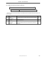
CONTENTS
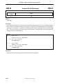
CHAPTER 1 INTRODUCTION................................................................................................................................... 1-1
1.1 Features ............................................................................................................................................................ 1-1
1.2 Ordering Information.......................................................................................................................................... 1-1
1.3 System Configuration ........................................................................................................................................ 1-2
1.4 Block Diagram (Summary)................................................................................................................................. 1-3
1.5 Block Diagram (Detail)....................................................................................................................................... 1-4
1.5.1 VR4120A RISC processor core................................................................................................................... 1-4
1.5.2 IBUS............................................................................................................................................................ 1-5
1.5.3 System controller ........................................................................................................................................ 1-6
1.5.4 <empty> ...................................................................................................................................................... 1-7
1.5.5 Ethernet controller....................................................................................................................................... 1-7
1.5.6 USB controller ............................................................................................................................................. 1-8
1.6 Pin Configuration (Bottom View)........................................................................................................................ 1-9
1.7 Pin Function..................................................................................................................................................... 1-11
1.7.1 System PLL power supply......................................................................................................................... 1-11
1.7.2 USB PLL power supply ............................................................................................................................. 1-11
1.7.3 System control interface............................................................................................................................ 1-12
1.7.4 System bus interface................................................................................................................................. 1-13
1.7.5 USB Interface............................................................................................................................................ 1-15
1.7.6 Ethernet interface...................................................................................................................................... 1-15
1.7.7 UART and Micro Wire interface................................................................................................................. 1-16
1.7.8 Parallel port interface ................................................................................................................................ 1-16
1.7.9 Boundary scan interface............................................................................................................................ 1-17
1.8 I/O Register Map.............................................................................................................................................. 1-18
1.9 Memory Map.................................................................................................................................................... 1-22
1.10 Reset Configuration ....................................................................................................................................... 1-23
1.11 Interrupts........................................................................................................................................................ 1-24
1.12 Clock Control Unit.......................................................................................................................................... 1-25
CHAPTER 2 VR4120A ............................................................................................................................................... 2-1
2.1 Overview for VR4120A ...................................................................................................................................... 2-1
2.1.1 Internal block configuration ......................................................................................................................... 2-2
2.1.2 VR4120A registers ...................................................................................................................................... 2-3
2.1.3 VR4120A instruction set overview............................................................................................................... 2-4
2.1.4 Data formats and addressing ...................................................................................................................... 2-4
2.1.5 Coprocessors (CP0).................................................................................................................................... 2-7
2.1.6 Floating-point unit (FPU) ............................................................................................................................. 2-8
2.1.7 CPU core memory management system (MMU)......................................................................................... 2-9
2.1.8 Translation lookaside buffer (TLB) .............................................................................................................. 2-9
2.1.9 Operating modes....................................................................................................................................... 2-10
2.1.10 Cache...................................................................................................................................................... 2-10
2.1.11 Instruction Pipeline.................................................................................................................................. 2-10
2.2 MIPS III Instruction Set Summary.................................................................................................................... 2-11
2.2.1 MIPS III ISA instruction formats ................................................................................................................ 2-11
2.2.2 Instruction classes..................................................................................................................................... 2-12
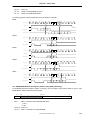
2.3 Pipeline............................................................................................................................................................ 2-29
Preliminary User’s Manual LAKI
A
2.3.1 Pipeline stages ..........................................................................................................................................2-29
2.3.2 Branch delay .............................................................................................................................................2-31
2.3.3 Load delay.................................................................................................................................................2-32
2.3.4 Pipeline operation......................................................................................................................................2-32
2.3.5 Interlock and exception handling ...............................................................................................................2-36
2.3.6 Program compatibility ................................................................................................................................2-43
2.4 Memory Management System .........................................................................................................................2-44
2.4.1 Translation lookaside buffer (TLB)............................................................................................................2-44
2.4.2 Virtual address space ................................................................................................................................2-45
2.4.3 Physical address space.............................................................................................................................2-57
2.4.4 System control coprocessor ......................................................................................................................2-58
2.4.5 CP0 registers.............................................................................................................................................2-60
2.5 Exception Processing......................................................................................................................................2-72
2.5.1 Exception processing operation ................................................................................................................2-72
2.5.2 Precision of exceptions..............................................................................................................................2-73
2.5.3 Exception processing registers..................................................................................................................2-73
2.5.4 Details of exceptions .................................................................................................................................2-86
2.5.5 Exception processing and servicing flowcharts .......................................................................................2-103
2.6 Initialization Interface .....................................................................................................................................2-110
2.6.1 Cold reset ................................................................................................................................................2-110
2.6.2 Soft reset .................................................................................................................................................2-110
2.6.3 VR4120A processor modes.....................................................................................................................2-110
2.7 Cache Memory...............................................................................................................................................2-113
2.7.1 Memory organization ...............................................................................................................................2-113
2.7.2 Cache organization..................................................................................................................................2-114
2.7.3 Cache operations ....................................................................................................................................2-116
2.7.4 Cache states ...........................................................................................................................................2-117
2.7.5 Cache state transition diagrams ..............................................................................................................2-118
2.7.6 Cache data integrity.................................................................................................................................2-119
2.7.7 Manipulation of the caches by an external agent ....................................................................................2-126
2.8 CPU Core Interrupts.......................................................................................................................................2-127
2.8.1 Non-maskable interrupt (NMI) .................................................................................................................2-127
2.8.2 Ordinary interrupts...................................................................................................................................2-127
2.8.3 Software interrupts generated in CPU core .............................................................................................2-127
2.8.4 Timer interrupt .........................................................................................................................................2-128
2.8.5 Asserting interrupts..................................................................................................................................2-128
CHAPTER 3 SYSTEM CONTROLLER .....................................................................................................................3-1
3.1 Overview ............................................................................................................................................................3-1
3.1.1 CPU interface ..............................................................................................................................................3-1
3.1.2 Memory interface.........................................................................................................................................3-1
3.1.3 IBUS interface .............................................................................................................................................3-1
3.1.4 UART...........................................................................................................................................................3-2
3.1.5 Microwire .....................................................................................................................................................3-2
3.1.6 Timer ...........................................................................................................................................................3-2
3.1.7 Interrupt controller .......................................................................................................................................3-2
3.1.8 DSU (Deadman’s SW UNIT) .......................................................................................................................3-2
3.1.9 General Purpose Input/Output Pins.............................................................................................................3-2
3.1.10 System block diagram ...............................................................................................................................3-3
B
Preliminary User’s Manual LAKI
3.1.11 Data flow diagram ..................................................................................................................................... 3-4
3.2 Registers............................................................................................................................................................ 3-5
3.2.1 Register summary ....................................................................................................................................... 3-5
3.2.2 General registers......................................................................................................................................... 3-7
3.3 CPU Interface .................................................................................................................................................. 3-20
3.3.1 Overview ................................................................................................................................................... 3-20
3.3.2 Data rate control........................................................................................................................................ 3-20
3.3.3 Address decoding ..................................................................................................................................... 3-20
3.3.4 Endian conversion..................................................................................................................................... 3-20
3.3.5 I/O performance ........................................................................................................................................ 3-22
3.4 Memory Interface............................................................................................................................................. 3-23
3.4.1 Overview ................................................................................................................................................... 3-23
3.4.2 Memory regions and devices .................................................................................................................... 3-23
3.1.3 Memory signal connections....................................................................................................................... 3-24
3.1.4 Memory performance ................................................................................................................................ 3-25
3.1.5 Memory control registers........................................................................................................................... 3-26
3.1.6 Boot ROM / Extended Chip Select ............................................................................................................ 3-33
3.1.7 SDRAM ..................................................................................................................................................... 3-37
3.1.8 SDRAM refresh ......................................................................................................................................... 3-40
3.1.9 Memory-to-CPU prefetch FIFO ................................................................................................................. 3-40
3.1.10 CPU-to-memory write FIFO..................................................................................................................... 3-40
3.1.11 SDRAM memory initialization.................................................................................................................. 3-41
3.5 IBUS Interface Register ................................................................................................................................... 3-42
3.5.1 ITCNTR (IBUS timeout timer control register) ........................................................................................... 3-42
3.5.2 ITSETR (IBUS timeout timer set register) ................................................................................................. 3-42
3.6 DSU (Deadman’s SW Unit) ............................................................................................................................. 3-43
3.6.1 Overview ................................................................................................................................................... 3-43
3.6.2 Registers ................................................................................................................................................... 3-43
3.6.3 DSU register setting flow........................................................................................................................... 3-44
3.7 Endian Mode Software Issues ......................................................................................................................... 3-45
3.7.1 Overview ................................................................................................................................................... 3-45
3.7.2 Endian modes ........................................................................................................................................... 3-45
CHAPTER 4 <empty> ................................................................................................................................................ 4-1
CHAPTER 5 ETHERNET CONTROLLER ................................................................................................................ 5-1
5.1 Overview............................................................................................................................................................ 5-1
5.1.1 Features ...................................................................................................................................................... 5-1
5.1.2 Block diagram of Ethernet controller block .................................................................................................. 5-1
5.2 Register ............................................................................................................................................................. 5-3
5.2.1 Statistics counter registers .......................................................................................................................... 5-4
5.2.2 DMA and FIFO management registers ....................................................................................................... 5-7
5.2.3 Interrupt and configuration registers............................................................................................................ 5-7
5.2.4 Detail of MAC control registers.................................................................................................................... 5-8
5.2.5 Detail of DMA and FIFO management registers ....................................................................................... 5-19
5.2.6 Detail of interrupt and configuration registers............................................................................................ 5-25
5.3 Operation......................................................................................................................................................... 5-27
5.3.1 Initialization ............................................................................................................................................... 5-27
5.3.2 Buffer structure for Ethernet block............................................................................................................. 5-27
5.3.3 Buffer descriptor format............................................................................................................................. 5-28
Preliminary User’s Manual LAKI
C
5.3.4 Frame transmission ...................................................................................................................................5-29
5.3.5 Frame reception ........................................................................................................................................5-32
CHAPTER 6 USB CONTROLLER.............................................................................................................................6-1
6.1 Overview ............................................................................................................................................................6-1
6.1.1 Features ......................................................................................................................................................6-1
6.1.2 Internal block diagram .................................................................................................................................6-2
6.2 Register Set .......................................................................................................................................................6-3
6.2.1 Register map ...............................................................................................................................................6-3
6.2.2 Explanation of registers ...............................................................................................................................6-4
6.3 USB Attachment Sequence .............................................................................................................................6-26
6.4 Initialization ......................................................................................................................................................6-27
6.4.1 Receive pool setting ..................................................................................................................................6-28
6.4.2 Send/receive mailbox setting.....................................................................................................................6-28
6.5 Data Send Function .........................................................................................................................................6-30
6.5.1 Overview of send processing ....................................................................................................................6-30
6.5.2 Send buffer configuration ..........................................................................................................................6-30
6.5.3 Data send modes ......................................................................................................................................6-33
6.5.4 VR4120A RISC processor processing at data sending .............................................................................6-34
6.5.5 USB controller processing at data sending................................................................................................6-37
6.5.6 Tx indication ..............................................................................................................................................6-39
6.6 Data Receive Function.....................................................................................................................................6-40
6.6.1 Overview of receive processing.................................................................................................................6-40
6.6.2 Receive buffer configuration......................................................................................................................6-41
6.6.3 Receive pool settings ................................................................................................................................6-43
6.6.4 Data receive mode ....................................................................................................................................6-44
6.6.5 VR4120A RISC processor receive processing ..........................................................................................6-47
6.6.6 USB controller receive processing.............................................................................................................6-48
6.6.7 Detection of errors on USB........................................................................................................................6-51
6.6.8 Rx data corruption on isochronous EndPoint ............................................................................................6-53
6.6.9 Rx FIFO overrun........................................................................................................................................6-54
6.6.10 Rx indication............................................................................................................................................6-55
6.7 Power Management .........................................................................................................................................6-57
6.7.1 Suspend ....................................................................................................................................................6-57
6.7.2 Resume .....................................................................................................................................................6-58
6.7.3 Remote wake up........................................................................................................................................6-59
6.8 Loopback Mode ...............................................................................................................................................6-60
6.9 Example of Connection ....................................................................................................................................6-61
CHAPTER 7 UART.....................................................................................................................................................7-1
7.1 Overview ............................................................................................................................................................7-1
7.2 UART Block Diagram .........................................................................................................................................7-1
7.3 UART Registers .................................................................................................................................................7-2
7.3.1 UART Receiver data Buffer Register (UARTRBR) (80H, DLAB = 0, R) ......................................................7-2
7.3.2 UART Interrupt Enable Register (UARTIER) (84H, DLAB = 1, R/W)...........................................................7-2
7.3.3 UART Divisor Latch LSB Register (UARTDLL) (80H, DLAB = 1, R/W) .......................................................7-3
7.3.4 UART Divisor Latch MSB Register (UARTDLM) (84H, DLAB = 1, R/W) .....................................................7-3
7.3.5 UART Interrupt ID Register (UARTIIR) (88H, R) .........................................................................................7-5
7.3.6 UART FIFO Control Register (UARTFCR) (88H, W) ...................................................................................7-6
7.3.7 UART Line Control Register (UARTLCR) (8CH, R/W) ................................................................................7-7
D
Preliminary User’s Manual LAKI
7.3.8 UART Modem Control Register (UARTMCR) (90H, R/W)........................................................................... 7-8
7.3.9 UART Line Status Register (UARTLSR) (94H, R/W) .................................................................................. 7-9
7.3.10 UART Modem Status Register (UARTMSR) (98H, R/W) ........................................................................ 7-10
7.3.11 UART Scratch Register (UARTSCR) (9CH, R/W)................................................................................... 7-11
CHAPTER 8 TIMER ................................................................................................................................................... 8-1
8.1 Overview............................................................................................................................................................ 8-1
8.2 Block Diagram ................................................................................................................................................... 8-1
8.3 Timer Registers ................................................................................................................................................. 8-2
8.3.1 Timer Mode Register (TMMR) (B0H, R/W) ................................................................................................. 8-2
8.3.2 Timer CH0 Count Set Register (TM0CSR) (B4H, R/W) .............................................................................. 8-2
8.3.3 Timer CH1 Count Set Register (TM1CSR) (B8H, R/W) .............................................................................. 8-2
8.3.4 Timer CH0 Current Count Register (TM0CCR) (BCH, R) ........................................................................... 8-2
8.3.5 Timer CH1 Current Count Register (TM1CCR) (C0H, R)............................................................................ 8-3
CHAPTER 9 MICRO WIRE ....................................................................................................................................... 9-1
9.1 Overview............................................................................................................................................................ 9-1
9.2 Micro Wire Connection ...................................................................................................................................... 9-1
9.3 Operations ......................................................................................................................................................... 9-1
9.3.1 Data read at the power up load ................................................................................................................... 9-1
9.3.2 Accessing to EEPROM ............................................................................................................................... 9-2
9.4 Registers............................................................................................................................................................ 9-2
9.4.1 ECCR (EEPROM Command Control Register) Address 1000_00D0H [Write Only] ................................. 9-2
9.4.2 ERDR (EEPROM Read Data Register) Address 1000_00D4H [Read Only]............................................. 9-3
9.4.3 MACAR1 (MAC Address Register 1) Address 1000_00D8H [Read Only] ................................................ 9-4
9.4.4 MACAR2 (MAC Address Register 2) Address 1000_00DCH [Read Only] ................................................ 9-4
9.4.5 MACAR3 (MAC Address Register 3) Address 1000_00E0H [Read Only]................................................. 9-4
APPENDIX A MIPS III INSTRUCTION SET DETAILS...........................................................................................A-1
A.1 Instruction Notation Conventions.....................................................................................................................A-1
A.2 Load and Store Instructions............................................................................................................................A-3
A.3 Jump and Branch Instructions ........................................................................................................................A-4
A.4 System Control Coprocessor (CP0) Instructions ...........................................................................................A-5
A.5 CPU Instruction ................................................................................................................................................A-5
A.6 CPU Instruction Opcode Bit Encoding.......................................................................................................A-158
APPENDIX B <empty>...............................................................................................................................................B-1
APPENDIX C VR4120A COPROCESSOR 0 HAZARDS ........................................................................................C-1
Preliminary User’s Manual LAKI
E
LIST OF FIGURES
Figure No. Title
Page
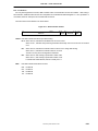
Figure 1-1. Examples of a LAKI System Configuration
1-2
Figure 1-2. Block Diagram of LAKI
1-3
Figure 1-3. Block Diagram of VR4120A RISC Processor
1-4
Figure 1-4. Block Diagram of IBUS
1-5
Figure 1-5. Block Diagram of System Controller
1-6
Figure 1-7. Block Diagram of Ethernet Controller
1-7
Figure 1-8. Block Diagram of USB Controller
1-8
Figure 1-9. Memory Map
1-22
Figure 1-10. Reset Configuration
1-23
Figure 1-11. Interrupt Signal Connection
1-24
Figure 1-12. Block Diagram of Clock Control Unit
1-25
Figure 2-1. VR4120A Core Internal Block Diagram
2-1
Figure 2-2. VR4120A Registers
2-3
Figure 2-3. CPU Instruction Formats (32-bit Length Instruction)
2-4
Figure 2-5. Little-Endian Byte Ordering in Word Data
2-5
Figure 2-6. Little-Endian Byte Ordering in Double Word Data
2-5
Figure 2-7. Misaligned Word Accessing (Little-Endian)
2-6
Figure 2-8. CP0 Registers
2-7
Figure 2-9. MIPS III ISA CPU Instruction Formats
2-11
Figure 2-10. Pipeline Stages (MIPS III Instruction Mode)
2-29
Figure 2-11. Instruction Execution in the Pipeline
2-30
Figure 2-14. Pipeline Activities (MIPS III)
2-30
Figure 2-16. Branch Delay (In MIPS III Instruction Mode)
2-31
F
Preliminary User’s Manual LAKI
Figure 2-18. ADD Instruction Pipeline Activities (In MIPS III Instruction Mode)
2-32
Figure 2-20. JALR Instruction Pipeline Activities (In MIPS III Instruction Mode)
2-33
Figure 2-22. BEQ Instruction Pipeline Activities (In MIPS III Instruction Mode)
2-34
Figure 2-24. TLT Instruction Pipeline Activities
2-34
Figure 2-25. LW Instruction Pipeline Activities (In MIPS III Instruction Mode)
2-35
Figure 2-27. SW Instruction Pipeline Activities (In MIPS III Instruction Mode)
2-36
Figure 2-29. Relationship among Interlocks, Exceptions, and Faults
2-36
Figure 2-30. Exception Detection
2-39
Figure 2-31. Data Cache Miss Stall
2-40
Figure 2-32. CACHE Instruction Stall
2-40
Figure 2-33. Load Data Interlock
2-41
Figure 2-34. MD Busy Interlock
2-41
Figure 2-35. Virtual-to-Physical Address Translation
2-45
Figure 2-36. 32-bit Mode Virtual Address Translation
2-46
Figure 2-37. 64-bit Mode Virtual Address Translation
2-47
Figure 2-38. User Mode Address Space
2-48
Figure 2-39. Supervisor Mode Address Space
2-50
Figure 2-40. Kernel Mode Address Space
2-52
Figure 2-41 LAKI Physical Address Space
2-57
Figure 2-42. CP0 Registers and TLB
2-58
Figure 2-43. Format of a TLB Entry
2-59
Figure 2-44. Index Register
2-60
Figure 2-45. Random Register
2-60
Figure 2-46. EntryLo0 and EntryLo1 Registers
2-61
Figure 2-47. Page Mask Register
2-62
Figure 2-48. Positions Indicated by Wired Register
2-63
Preliminary User’s Manual LAKI
G
Figure 2-49. Wired Register
2-63
Figure 2-50. EntryHi Register
2-64
Figure 2-51. PRId Register
2-65
Figure 2-52. Config Register Format
2-66
Figure 2-53. LLAddr Register
2-67
Figure 2-54. TagLo Register
2-68
Figure 2-55. TagHi Register
2-68
Figure 2-56. TLB Address Translation
2-70
Figure 2-57. Context Register Format
2-74
Figure 2-58. BadVAddr Register Format
2-75
Figure 2-59. Count Register Format
2-75
Figure 2-60. Compare Register Format
2-76
Figure 2-61. Status Register Format
2-77
Figure 2-62. Status Register Diagnostic Status Field
2-78
Figure 2-63. Cause Register Format
2-79
Figure 2-64. EPC Register Format (When MIPS16 ISA Is Disabled)
2-81
Figure 2-65. EPC Register Format (When MIPS16 ISA Is Enabled)
2-82
(a) 32-bit mode
2-82
(b) 64-bit mode
2-82
Figure 2-66. WatchLo Register Format
2-82
Figure 2-67. WatchHi Register Format
2-82
Figure 2-68. XContext Register Format
2-83
Figure 2-69. Parity Error Register Format
2-83
Figure 2-70. Cache Error Register Format
2-84
Figure 2-71. ErrorEPC Register Format (When MIPS16 ISA Is Disabled)
2-85
Figure 2-72. ErrorEPC Register Format (When MIPS16 ISA Is Enabled)
2-85
H
Preliminary User’s Manual LAKI
(a) 32-bit mode
2-85
(b) 64-bit mode
2-85
Figure 2-73. Common Exception Handling (1/2)
2-104
(a) Handling Exceptions other than Cold Reset, Soft Reset, NMI, and TLB/XTLB Refill (Hardware)
2-104
Figure 2-73. Common Exception Handling (2/2)
2-105
(b) Servicing Common Exceptions (Software)
2-105
Figure 2-74. TLB/XTLB Refill Exception Handling (1/2)
2-106
(a) Handling TLB/XTLB Refill Exceptions (Hardware)
2-106
Figure 2-74. TLB/XTLB Refill Exception Handling (2/2)
2-107
(b) Servicing TLB/XTLB Refill Exceptions (Software)
2-107
Figure 2-75. Cold Reset Exception Handling
2-108
Figure 2-76. Soft Reset and NMI Exception Handling
2-109
Figure 2-77. Logical Hierarchy of Memory
2-113
Figure 2-78. Cache Support
2-114
Figure 2-79. Instruction Cache Organization and Line Format
2-115
Figure 2-80. Data Cache Organization and Line Format
2-115
Figure 2-81. Cache Data and Tag Organization
2-116
Figure 2-82. Data Cache State Diagram
2-118
Figure 2-83. Instruction Cache State Diagram
2-118
Figure 2-84. Data Check Flow on Instruction Fetch
2-119
Figure 2-85. Data Check Flow on Load Operations
2-119
Figure 2-86. Data Check Flow on Store Operations
2-120
Figure 2-87. Data Check Flow on Index_Invalidate Operations
2-120
Figure 2-88. Data Check Flow on Index_Writeback_Invalidate Operations
2-121
Figure 2-89. Data Check Flow on Index_Load_Tag Operations
2-121
Figure 2-90. Data Check Flow on Index_Store_Tag Operations
2-122
Preliminary User’s Manual LAKI
I
Figure 2-91. Data Check Flow on Create_Dirty Operations
2-122
Figure 2-92. Data Check Flow on Hit_Invalidate Operations
2-123
Figure 2-93. Data Check Flow on Hit_Writeback_Invalidate Operations
2-123
Figure 2-94. Data Check Flow on Fill Operations
2-124
Figure 2-95. Data Check Flow on Hit_Writeback Operations
2-124
Figure 2-96. Writeback Flow
2-125
Figure 2-97. Refill Flow
2-125
Figure 2-98. Writeback & Refill Flow
2-126
Figure 2-99. Non-maskable Interrupt Signal
2-127
Figure 2-100. Hardware Interrupt Signals
2-128
Figure 2-101. Masking of Interrupt Request Signals
2-129
Figure 3-1. Bit and Byte Order of Endian Modes
3-46
Figure 3-2. Halfword Data-Array Example
3-46
Figure 3-3. Word Data-Array Example
3-47
Figure 5-1. Block Diagram of Ethernet Controller
5-2
Figure 5-2. Tx FIFO Control Mechanism
5-20
Figure 5-3. Rx FIFO Control Mechanism
5-23
Figure 5-4. Buffer Structure for Ethernet Block
5-27
Figure 5-5. Transmit Descriptor Format
5-28
Figure 5-6. Receive Descriptor Format
5-28
Figure 5-7. Transmit Procedure
5-31
Figure 5-8. Receive Procedure
5-33
Figure 6-1. USB Controller Internal Configuration
6-2
Figure 6-2. USB Attachment Sequence
6-26
Figure 6-3. Mailbox Configuration
6-29
Figure 6-4. Division of Data into USB Packets
6-30
J
Preliminary User’s Manual LAKI
Figure 6-5. Send Buffer Configuration
6-31
Figure 6-6. Configuration of Send Packet Descriptors
6-32
Figure 6-7. VR4120A RISC Processor Processing at Data Sending
6-34
Figure 6-8. Send Command Issue
6-35
Figure 6-9. Send Status Register
6-36
Figure 6-10. USB Controller Send Operation Flow Chart
6-37
Figure 6-11. Send Indication Format
6-39
Figure 6-12. Division of Data into USB Packets
6-40
Figure 6-13. Receive Pool Configuration
6-41
Figure 6-14. Receive Descriptor Configuration
6-42
Figure 6-15. Buffer Directory Addition Command
6-44
Figure 6-16. Data Receiving in EndPoint0, EndPoint6
6-45
Figure 6-17. EndPoint2, EndPoint4 Receive Normal Mode
6-45
Figure 6-18. EndPoint2, EndPoint4 Receive Assemble Mode
6-46
Figure 6-19. EndPoint2, EndPoint4 Receive Separate Mode
6-46
Figure 6-20. VR4120A RISC Processor Receive Processing
6-47
Figure 6-21. USB Controller Receive Operations (Assemble Mode)
6-48
Figure 6-22. USB Controller Receive Operation Sequence (Separate Mode)
6-50
Figure 6-23. USB Timing Errors
6-51
Figure 6-24. Example of Buffers Including Corrupted Data
6-54
Figure 6-25. Receive Indication Format
6-55
Figure 6-26. Suspend Sequence
6-57
Figure 6-27. Resume Sequence
6-58
Figure 6-28. Remote Wake Up Sequence
6-59
Figure 6-29. Data Flow in Loopback Mode
6-60
Figure 6-30. Example of Connection
6-61
Preliminary User’s Manual LAKI
K
Figure A-1. VR4120A Opcode Bit Encoding (1/2)
A-158
Figure A-1. VR4120AOpcode Bit Encoding (2/2)
A-159
L
Preliminary User’s Manual LAKI
LIST OF TABLES
Table No.
Title
Page
Table 2-1. System Control Coprocessor (CP0) Register Definitions
2-8
Table 2-2. Number of Delay Slot Cycles Necessary for Load and Store Instructions
2-12
Table 2-3. Byte Specification Related to Load and Store Instructions
2-13
Table 2-4. Load/Store Instruction
2-14
Table 2-5. Load/Store Instruction (Extended ISA)
2-15
Table 2-6. ALU Immediate Instruction
2-16
Table 2-7. ALU Immediate Instruction (Extended ISA)
2-17
Table 2-8. Three-Operand Type Instruction
2-17
Table 2-9. Three-Operand Type Instruction (Extended ISA)
2-18
Table 2-10. Shift Instruction
2-18
Table 2-11. Shift Instruction (Extended ISA)
2-19
Table 2-12. Multiply/Divide Instructions
2-20
Table 2-13. Multiply/Divide Instructions (Extended ISA)
2-21
Table 2-14. Number of Stall Cycles in Multiply and Divide Instructions
2-22
Table 2-15. Number of Delay Slot Cycles in Jump and Branch Instructions
2-22
Table 2-16. Jump Instruction
2-23
Table 2-17. Branch Instructions
2-24
Table 2-18. Branch Instructions (Extended ISA)
2-25
Table 2-19. Special Instructions
2-26
Table 2-20. Special Instructions (Expanded ISA) (1/2)
2-26
Table 2-20. Special Instructions (Expanded ISA) (2/2)
2-27
Table 2-21. System Control Coprocessor (CP0) Instructions (1/2)
2-27
Table 2-21. System Control Coprocessor (CP0) Instructions (2/2)
2-28
Preliminary User’s Manual LAKI
M
Table 2-42. Operation in Each Stage of Pipeline (MIPS III)
2-30
Table 2-44. Correspondence of Pipeline Stage to Interlock and Exception Conditions
2-36
Table 2-45. Pipeline Interlock
2-37
Table 2-46. Description of Pipeline Exception
2-37
Table 2-47. VR Series Supported Instructions
2-43
Table 2-48. Comparison of useg and xuseg
2-49
Table 2-49. 32-bit and 64-bit Supervisor Mode Segments
2-50
Table 2-50. 32-bit Kernel Mode Segments
2-53
Table 2-51. 64-bit Kernel Mode Segments
2-54
Table 2-52. Cacheability and xkphys Address Space
2-55
Table 2-54. Cache Algorithm
2-62
Table 2-55. Mask Values and Page Sizes
2-62
Table 2-56. CP0 Exception Processing Registers
2-73
Table 2-57. Cause Register Exception Code Field
2-79
Table 2-58. 64-Bit Mode Exception Vector Base Addresses
2-86
Table 2-59. 32-Bit Mode Exception Vector Base Addresses
2-87
Table 2-60. Exception Priority Order
2-88
Table 3-1. Endian Configuration Table
3-21
Table 3-2. Endian Translation Table in Endian Converter
3-21
Table 3-3. External Pin Mapping
3-24
Table 3-4. Examples of Memory Performance (4word-burst access from CPU)
3-25
Table 3-5. Examples of Memory Performance (4word-burst access from IBUS Master)
3-25
Table 3-6. Boot-ROM Size Configuration at Reset
3-33
Table 3-7. Command Sequence
3-34
(a) Program Command Sequence (4 Write Cycles)
3-34
(b) Chip Erase Command Sequence (6 Write Cycles)
3-34
N
Preliminary User’s Manual LAKI
(c) Sector Erase Command Sequence (6 Write Cycles)
3-34
Table 3-8. Relationship between memory map and address bus
3-36
Table 3-9. SDRAM Size Configuration at Reset
3-37
Table 3-10. SDRAM Configurations Supported
3-37
Table 3-11. SDRAM Bank Select Signals Mapping
3-37
Table 3-12. SDRAM Word Order for Instruction-Cache Line-Fill
3-38
Table 5-1. Ethernet Controller’s Register Map
5-3
Table 5-2. MAC Control Register Map
5-4
Table 5-3. Statistics Counter Register Map
5-5
Table 5-4. DMA and FIFO Management Registers Map
5-7
Table 5-5. Interrupt and Configuration Registers Map
5-7
Table 5-6. Attribute for Transmit Descriptor
5-28
Table 5-7. Attribute for Receive Descriptor
5-29
Table 7-1. Correspondence between Baud Rates and Divisors
7-4
Table 9-1. EEPROM Initial Data
9-2
Table 9-2. EEPROM Command List
9-2
Table A-1. CPU Instruction Operation Notations
A-2
Table A-2. Load and Store Common Functions
A-3
Table A-3. Access Type Specifications for Loads/Stores
A-4
Table C-1. VR4120A CPU Coprocessor 0 Hazards
C-2
Table C-2. Calculation Example of CP0 Hazard and Number of Instructions Inserted
C-5
Preliminary User’s Manual LAKI
O
[MEMO]
P
Preliminary User’s Manual LAKI
PREFACE
Readers
This manual is intended for engineers who need to be familiar with the capability of
LAKI in order to develop application systems based on it.
Purpose
The purpose of this manual is to help users understand the hardware capabilities
(listed below) of the LAKI.
Configuration
This manual consists of the following chapters:
• Introduction
• VR4120A CPU
• System controller
• Ethernet controller
• USB controller
• UART
• Timer
• Micro Wire
• General Purpose Input/Output
Guidance
Readers of this manual should already have a general knowledge of electronics, logic
circuits, and microcomputers.
To gain an overall understanding of the function of the LAKI:
→ Read through all the chapters, in sequence.
To check the electrical characteristics of the LAKI:
→ Refer to the separate data sheet.
Any remaining reference to the µPD98501 (KORVA) device in this manual should be
interpreted as "LAKI", which is functional equivalent in these cases.
Notation
This manual uses the following conventions:
Data bit significance:
High-order bits on the left side;
low-order bits on the right side
Active low:
XXXX_B (Pin and signal names are suffixed with _B.)
Note:
Explanation of an indicated part of text
Caution:
Information requiring the user’s special attention
Remark:
Supplementary information
Numerical value:
Binary ... xxxx or xxxxB
Decimal ... xxxx
Hexadecimal ... xxxxH
Related Document
Use this manual in combination with the following document.
The related documents indicated in this publication may include preliminary versions.
However, preliminary versions are not marked as such.
• LAKI Data Sheet: To be prepared
Preliminary User’s Manual LAKI
i
[MEMO]
ii
Preliminary User’s Manual LAKI
CHAPTER 1 INTRODUCTION
LAKI is a high performance controller which includes high performance MIPS based 64bit RISC processor
VR4120A CPU core, Ethernet Controller, USB controller Block and SDRAM interface.
1.1 Features
• Includes high performance MIPS based 64-bit RISC processor VR4120A
• Can perform RTOS and network middleware (M/W) on the chip
• Includes interface for PROM and flash ROM used for storing boot program
• Includes single 10/100Mbps Ethernet controller compliant to IEEE802.3,IEEE 802.3u and IEEE802.3x
• Can directly connect external Ethernet PHY device through 3.3V MII interface
• Includes USB full speed function controller compliant to USB specification 1.1
• Supports operation conforming to the USB Communication Device Class Specification
• Can directly connect 64Mbit and 128Mbit SDRAM as external memory
• Includes boundary scan function(JTAG) compliant to IEEE 1149.1
• Includes Micro Wire interface
• Includes 2ch general purpose timers
• Using advanced CMOS technology
• Supply Voltage 2.5V (required 3.3V supply for 3.3V interface)
• Package T-BGA-256
1.2 Ordering Information
Part Number
µPD98503N7-B6
Package
256 pin TBGA
Preliminary User’s Manual LAKI
1-1
CHAPTER 1 INTRODUCTION
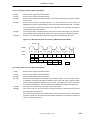
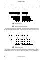
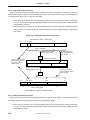
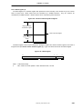
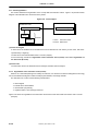
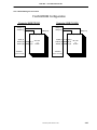
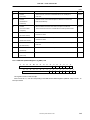
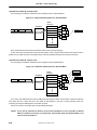
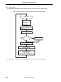
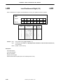
1.3 System Configuration
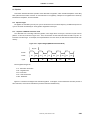
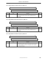
LAKI can perform as a network controller for arbitrary applications, requiring a high performance CPU to run
network protocol stacks, an Ethernet or USB Communication Class interface and a powerful bus interface which
allows the connection of external devices and memories. USB and Ethernet functions will exclusively operate each
other.
Figure 1-1. Examples of a LAKI System Configuration
Example1. Powerline Communication Modem
USB
PLC
Modem
LAKI
Analog
Front
End
Powerline
PC
System Bus
FLASH
SDRAM
Example2. Powerline Communication Router
100B-T
PLC
Modem
LAKI
Analog
Front
End
Powerline
HUB
System Bus
FLASH
SDRAM
PC
PC/Printer
Example3. USB/Ethernet Network Protocol Client Controller
100B-T
or
USB
Glue
I/O
LAKI
Glue
System Bus
SDRAM
1-2
FLASH
Preliminary User’s Manual LAKI
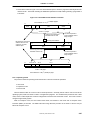
CHAPTER 1 INTRODUCTION
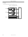
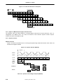
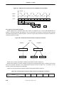
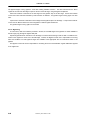
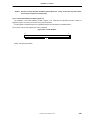
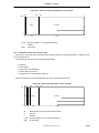
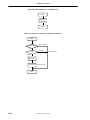
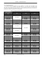
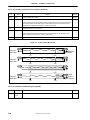
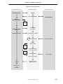
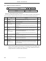
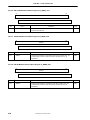
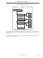
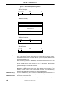
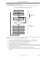
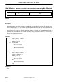
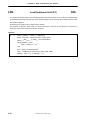
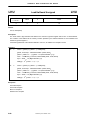
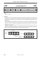
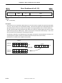
1.4 Block Diagram (Summary)
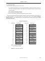
Figure 1-2. Block Diagram of LAKI
USB
MIPS
Core with
16K Instruction and
8K Data Cache
Full Speed USB
Function Controller
DMA
Control, Interrupt etc.
Extended JTAG
ETHERNET
MAC
DMA
IBUS
PROM / FLASH
3,3V MII
System Controller
with
Memory Controller
SDRAM
IO Bus
and
JTAG
JTAG
Controller
CLOCK
Control
Unit
RS232
low speed bus section
for
UART, Timer, GPIO
Preliminary User’s Manual LAKI
GPIO
1-3
CHAPTER 1 INTRODUCTION
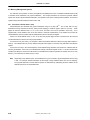
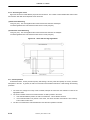
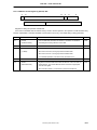
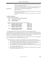
1.5 Block Diagram (Detail)
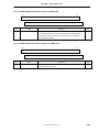
1.5.1 VR4120A RISC processor core
NEC will support real-time OS running on the high performance VR4120A RISC processor core. The core can
perform network protocols (TCP/IP, PPP, SNMP, HTTP etc) to realize the targeted network control function.
Middlewares including RTOS will be loaded to SDRAM from external PROM and Flash ROM and by setting write
protected area for such a area, high speed processing will be realized together with large size instruction cache.
Features of VR4120A RISC Processor Core are as follows;
• MIPS/I/II/III instruction set will be supported (FPU, LL, LLD, SC, SCD instruction will be excluded)
• Realize high speed processing of application by supporting high speed multiply and accumulate function
• Includes Large size cache memory (Instruction:16kbytes, Data:8kbytes)
• Supports up to 1T byte virtual address space by using full associative TLB
• Implements switching function between Big-Endian and Little-Endian
Figure 1-3. Block Diagram of VR4120A RISC Processor
VR4120 RISC Processor Core
VR4120 DATA PATH
DATA
CACHE
(8kBytes)
INSTRUCTION
CACHE
(16kBytes)
On Chip
Debugger
N-wire
BUS Controller
SysAD BUS
1-4
Preliminary User’s Manual LAKI
CHAPTER 1 INTRODUCTION
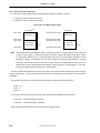
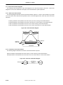
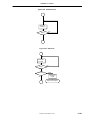
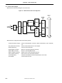
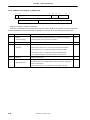
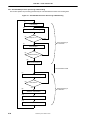
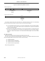
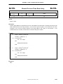
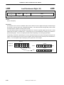
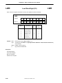
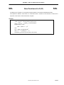
1.5.2 IBUS
The IBUS is a 32-bit, 66-MHz high-speed on-chip bus which enables interconnection between itself and IBUS(64bit bus).
The IBUS supports the following bus protocols;
• Single read/write transfer
• Burst read/write transfer
• Slave lock
• Retry and disconnect
• Bus parking
Figure 1-4. Block Diagram of IBUS
IBUS Interface Block
IBUS
IBUS
arbiter
BUS MASTER
System
Controller
IBUS
Master
I/F
Ethernet
Controller
USB
Controller
IBUS
MUX
IBUS
Slave
I/F
decoder
BUS SLAVE
(Using MUX Bus Arrangement)
Preliminary User’s Manual LAKI
1-5
CHAPTER 1 INTRODUCTION
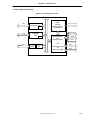
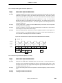
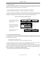
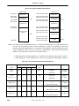
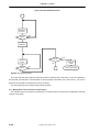
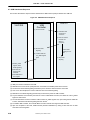
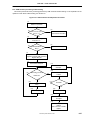
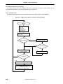
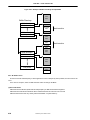
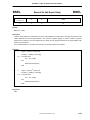
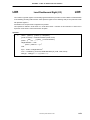
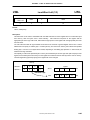
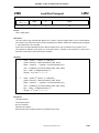
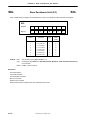
1.5.3 System controller
System controller is LAKI’s internal system controller. It provides bridging function among the VR4120A System
Bus “SysAD”, NEC original high speed on-chip bus “IBUS” and the system bus for SDRAM/PROM/FLASH and
external expansions.
Features of System controller are as follows;
• Implements 4word prefetch FIFO buffer between SysAD and Memory
• Implements 32bit×64word FIFO buffer for each TX and RX between IBUS and Memory.
• Implements 32bit× 4word command buffer to IBUS from VR4120A
• Provides bus bridging function among SysAD bus and IBUS(internal bus) and MEMORY
• Supports Endian Converting function on SysAD bus
• Can directly connect 64Mbit/128Mbit SDRAM(MAX.32MBytes) and PROM/FLASH(MAX.8MBytes) memory
• Supports all VR4120A bus cycles at 66MHz or 100MHz
• PROM/FLASH data signals multiplexed on SDRAM data signals
• Supports 266 MB/sec (32bit @66MHz) bursts on IBUS
• Generates NMI and INT
• Supports Universal Asynchronous Receiver/Transmitter(UART)
• Supports separated 2ch Timer
• Supports Deadmans Switch Unit(Watch Dog Timer)
• Supports general purpose input/output pins
• Supports Micro Wire interface
Figure 1-5. Block Diagram of System Controller
SysAD
STAR
MIF
HIF
SysAD-IF
Prefetch
Buffer
SysAD-IF
Write
Buffer
REGISTER
FLASH
PROM
(External
devices)
SDRAM
FLASH-IF
SDRAM-IF
Memory
Arbitor
Write
Write
BufferWrite
BufferWrite
Buffer
Buffer
General
purpose
I/O
TIMER
UART
RS232C
DSU
64word
Write
FIFO
64word
Write
FIFO
MicroWire
Read
Buffer
IBUS32 Slave-IF
IBUS32 Master-IF
IBUS32
1-6
Preliminary User’s Manual LAKI
E2PROM
CHAPTER 1 INTRODUCTION
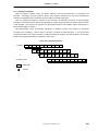
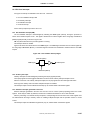
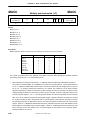
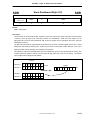
1.5.4 <empty>
1.5.5 Ethernet controller
Ethernet Controller supports single channel 10Mbps/100Mbps Ethernet MAC (Media Access Control) function and
MII (Media Independent Interface) function
Features of Ethernet Controller are as follows;
• Supports 10M/100M Ethernet MAC function compliant to IEEE802.3 and IEEE802.3u
• Supports 3.3V MII compliant to IEEE802.3u
• Supports full duplex operation for both 100Mbps and 10Mbps
• Supports flow control function compliant to IEEE802.3x/D3.2
• Implements 256Byte FIFO buffer for each TX and RX
• Implements address filtering functions for unicast/multicast/broadcast
• Implements MIB counters for network management (MIB II, Ether-like MIB,IEEE802.3LME are supported)
• Supports loopback function within MII interface
• Implements local DMA controller with individual DMA channels for each TX and RX
Figure 1-7. Block Diagram of Ethernet Controller
Ethernet Controller
Transceiver
TPO+
TPO-
MII
MII
I/O BUF
I/O BUF
MAC
MAC
CORE
CORE
(NAFMAC)
(NAFMAC)
Tx FIFO
Tx FIFO
Rx FIFO
Rx FIFO
DMAC
DMAC
IBUS
Controller
TPI+
TPI-
MII
IBUS
FIFO
FIFO
Cont.
Cont.
Preliminary User’s Manual LAKI
1-7
CHAPTER 1 INTRODUCTION
1.5.6 USB controller
USB Controller provides Full Speed Function device function defined in Universal Serial Bus.
Features of USB Controller are as follows;
• Compliant to Universal Serial Bus Specification Rev1.1
• Supports xDSL Sub Class function compliant to Communication Class Definition
• Supports Device class function by software running on V R4120A core
• Performs 12Mbps Full Speed USB function device (Hub function will be not supported)
• Can handle Suspend, Resume and Wake-up management signaling
• Supports Remote Wake-up.
• Implements 7 kinds of endpoints (Control, Interrupt IN/OUT, Isochronous IN/OUT, Bulk IN/OUT)
• Implements 64Bytes FIFO buffer used for Control transfer for TX
• Implements 128Bytes FIFO buffer used for Isochronous transfer for TX
• Implements 128Bytes FIFO buffer used for Bulk transfer for TX
• Implements 64Bytes FIFO buffer used for Interrupt transfer for TX
• Implements 128Bytes shared FIFO buffer used for Control/Isochronous/Bulk/Interrupt transfer for RX
• Implements local DMAC(DMA controller) block
• Can directly connect USB connector through USB dedicated I/O buffer
Figure 1-8. Block Diagram of USB Controller
USB Controller
EPFIFO
EPFIFO
DMAC
DMAC
IBUS
Controller
D+
USB
D-
I/O
I/O
Buf
Buf
SIE
SIE
EPC
EPC
MCONT
MCONT
1-8
Preliminary User’s Manual LAKI
IBUS
CHAPTER 1 INTRODUCTION
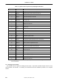
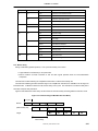
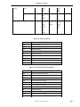
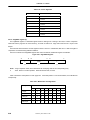
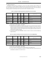
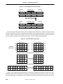
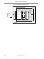
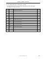
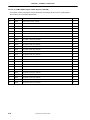
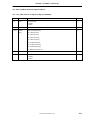
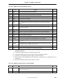
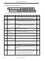
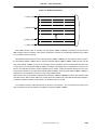
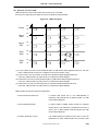
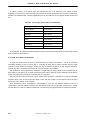
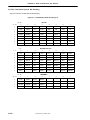
1.6 Pin Configuration (Bottom View)
• 256-pin Tape BGA (27mm x 27mm)
product code: µPD98503N7-B6
Preliminary User’s Manual LAKI
1-9
CHAPTER 1 INTRODUCTION
Pin Name
Pin No.
A01
A02
A03
A04
A05
A06
A07
A08
A09
A10
A11
A12
A13
A14
A15
A16
A17
A18
A19
A20
B01
B02
B03
B04
B05
B06
B07
B08
B09
B10
B11
B12
B13
B14
B15
B16
B17
B18
B19
B20
C01
C02
C03
C04
C05
C06
C07
C08
C09
C10
C11
C12
Pin Name
IC-PDn
IC-Open
ENDCEN
RMSL0
GPIO0
GPIO4
GPIO6
GPIO8
EXNMI
GPIO13
GPIO14
MWDI
MWDO
URDCD
URDTR
SMA1
SMA3
SMA5
SMA8
SMA9
IC-PUp
IC-PDn
IC-PDn
IC-PDn
RMSL1
GPIO3
GPIO5
GPIO7
GPIO11
GPIO12
GPIO15
MWCS
URCTS
URCLK
URSDO
SMA2
GND
SMA7
SMA10
SMA11
IC-Open
IC-PDnR
VDD2
GND
BIG
GPIO2
VDD2
GND
GPIO10
VDD2
EXINT
GND
Pin No.
C13
C14
C15
C16
C17
C18
C19
C20
D01
D02
D03
D04
D05
D06
D07
D08
D09
D10
D11
D12
D13
D14
D15
D16
D17
D18
D19
D20
E01
E02
E03
E04
E17
E18
E19
E20
F01
F02
F03
F04
F17
F18
F19
F20
G01
G02
G03
G04
G17
G18
G19
G20
Pin Name
URDSR
VDD2
URSDI
SMA4
SMA6
VDD2
SMA12
SMA14
GND
IC-Open
IC-Open
GND
VDD3
GPIO1
GND
VDD3
GPIO9
GND
VDD3
MWSK
URRTS
GND
SMA0
VDD3
GND
SMA13
SMA15
SMA16
GND
VDD2
IC-Open
IC-Open
VDD3
GND
SMA17
SMA18
IC-PDn
IC-PDn
IC-PDn
IC-Open
SMA19
SMA20
SRMOE
SRMCS
IC-PDn
IC-PDn
VDD2
GND
GND
VDD2
SEXCS0
SEXCS1
Pin No.
H01
H02
H03
H04
H17
H18
H19
H20
J01
J02
J03
J04
J17
J18
J19
J20
K01
K02
K03
K04
K17
K18
K19
K20
L01
L02
L03
L04
L17
L18
L19
L20
M01
M02
M03
M04
M17
M18
M19
M20
N01
N02
N03
N04
N17
N18
N19
N20
P01
P02
P03
P04
Pin Name
GND
VDD2
GND
VDD3
VDD3
GND
SEXCS2
SDCS
IC-PDn
IC-PDn
IC-Open
IC-Open
SDCKE1
SDRAS
SDCKE0
SDCLK0
IC-PDn
IC-PDn
GND
VDD2
GND
VDD2
SDCLK1
GND
IC-PUp
IC-PDn
VDD2
GND
SDWE
IC-PDn
VDD3
SDCAS
IC-PDn
IC-PDn
VDD2
GND
GND
SMD2
SMD1
SMD0
GND
MIMD
MIRD0
VDD3
VDD3
SMD5
SMD4
SMD3
MIRD1
MIRD2
VDD2
GND
Special pin name description:
IC-PDn:
Pull Down
IC-PDnR:
Pull Down with Resistor
IC-PUp:
Pull Up
IC-PUpR:
Pull Up with Resistor
IC-Open:
Test output shall be left open
1-10
Preliminary User’s Manual LAKI
Pin No.
P17
P18
P19
P20
R01
R02
R03
R04
R17
R18
R19
R29
T01
T02
T03
T04
T17
T18
T19
T20
U01
U02
U03
U04
U05
U06
U07
U08
U09
U10
U11
U12
U13
U14
U15
U16
U17
U18
U19
U20
V01
V02
V03
V04
V05
V06
V07
V08
V09
V10
V11
V12
Pin Name
GND
VDD2
SMD7
SMD6
MIRD3
MIRER
MIRDV
MITD0
SMD11
SMD10
SMD9
SMD8
MITD1
MITD2
MICRS
GND
VDD3
SMD14
SMD12
GND
MITD3
MIRCLK
IC-PDn
GND
JDO
IC-PUp
GND
IC-Open
PSDVD
PUDGND
GND
VDD3
GND
GND
SMD30
VDD3
GND
SMD17
SMD15
SMD13
MITCLK
MICOL
VDD2
JCK
VDD3
IC-PUp
VDD2
PSDGND
PUDVD
IC-PDn
VDD2
USBDM
Pin No.
V13
V14
V15
V16
V17
V18
V19
V20
W01
W02
W03
W04
W05
W06
W07
W08
W09
W10
W11
W12
W13
W14
W15
W16
W17
W18
W19
W20
Y01
Y02
Y03
Y04
Y05
Y06
Y07
Y08
Y09
Y10
Y11
Y12
Y13
Y14
Y15
Y16
Y17
Y18
Y19
Y20
Pin Name
VDD2
VDD2
SMD31
SMD27
SMD24
VDD2
SMD18
SMD16
MITER
MITE
GND
JDI
RSTB
CLKSL
SCLK
PSAGND
PUAVD
PUSTBY
IC-PDn
USBDP
IC-Open
IC-PDn
IC-PDn
GND
SMD26
SMD23
SMD21
SMD19
MIMCLK
IC-Open
JMS
JRSTB
IC-PUp
IC-PDn
PSTBY
PSAVD
PUAGND
IC-Open
USBCLK
VDD3
IC-Open
IC-Open
IC-PDn
SMD29
SMD28
SMD25
SMD22
SMD20
CHAPTER 1 INTRODUCTION
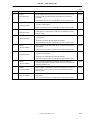
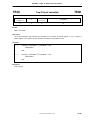
1.7 Pin Function
Symbol of I/O column indicates following status in this section.
I
:Input
O
:Output
I/O
:Bidirection
I/OZ :Bidirection (Include Hi-Z state)
I/OD :Bidirection (Open drain output)
OZ :Output (Include Hi-Z state)
OD :Output (Open drain)
1.7.1 System PLL power supply
Pin Name
Pin No.
I/O
Active Level
Function
PSAGND
100
Analog ground
PSAVD
27
Analog power supply
PSDGND
165
Digital ground
PSDVD
223
Digital power supply
1.7.2 USB PLL power supply
Pin Name
Pin No.
I/O
Active Level
Function
PUAGND
28
Analog ground
PUAVD
101
Analog power supply
PUDGND
224
Digital ground
PUDVD
166
Digital power supply
Preliminary User’s Manual LAKI
1-11
CHAPTER 1 INTRODUCTION
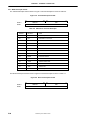
1.7.3 System control interface
Pin Name
Pin No.
I/O
Active Level
Function
SCLK
99
I
System clock (33MHz)
CLKSL
98
I
Clock select (100MHz/66MHz)
PSTBY
26
I
H
System PLL standby mode control input
PUSTBY
102
I
H
USB PLL Standby mode control
BIG
203
I
H
VR4120A Bigendian mode
ENDCEN
75
I
EXINT_B
197
I
L
External interrupt
EXNMI_B
69
I
L
External non-maskable interrupt
RST_B
97
I
L
System reset
ROMSEL0
74
I
ROM access bus width
ROMSEL1
142
I
(ROMSEL1/0=L/L;32bit, L/H;16bit, H/L;8bit)
1-12
Big Endian mode enable
Preliminary User’s Manual LAKI
CHAPTER 1 INTRODUCTION
1.7.4 System bus interface
(1/2)
Pin Name
Pin No.
I/O
Active Level
Function
SDCLK0
50
O
SDRAM Clock
SDCLK1
120
O
SDRAM Clock
SDCKE0
121
O
H
SDRAM Clock Enable
SDCKE1
239
O
H
SDRAM Clock Enable
SDCS_B
51
O
L
SDRAM Chip select
SDRAS_B
184
O
L
SDRAM Row address strobe
SDCAS_B
48
O
L
SDRAM Column address strobe
SDWE_B
237
O
L
SDRAM/PROM/FLASH write enable
SRMCS_B
53
O
L
PROM/FLASH chip select
SRMOE_B
124
O
L
PROM/FLASH output enable
SEXCS0_B
123
O
L
Extended Chip Select 0
SEXCS1_B
52
O
L
Extended Chip Select 1
SEXCS2_B
122
O
L
Extended Chip Select 2
SMA0
246
O
System Bus Address
SMA1
62
O
System Bus Address
SMA2
131
O
System Bus Address
SMA3
61
O
System Bus Address
SMA4
192
O
System Bus Address
SMA5
60
O
System Bus Address
SMA6
191
O
System Bus Address
SMA7
129
O
System Bus Address
SMA8
59
O
System Bus Address
SMA9
58
O
System Bus Address
SMA10
128
O
System Bus Address
SMA11
57
O
System Bus Address
SMA12
127
O
System Bus Address
SMA13
189
O
System Bus Address
SMA14
56
O
System Bus Address
SMA15
126
O
System Bus Address
SMA16
55
O
System Bus Address
SMA17
125
O
System Bus Address
SMA18
54
O
System Bus Address
SMA19
242
O
System Bus Address
SMA20
187
O
System Bus Address
Preliminary User’s Manual LAKI
1-13
CHAPTER 1 INTRODUCTION
(2/2)
Pin Name
Pin No.
I/O
SMD0
47
I/O
System Bus data
SMD1
118
I/O
System Bus data
SMD2
181
I/O
System Bus data
SMD3
46
I/O
System Bus data
SMD4
117
I/O
System Bus data
SMD5
180
I/O
System Bus data
SMD6
45
I/O
System Bus data
SMD7
116
I/O
System Bus data
SMD8
44
I/O
System Bus data
SMD9
115
I/O
System Bus data
SMD10
178
I/O
System Bus data
SMD11
233
I/O
System Bus data
SMD12
114
I/O
System Bus data
SMD13
42
I/O
System Bus data
SMD14
177
I/O
System Bus data
SMD15
113
I/O
System Bus data
SMD16
41
I/O
System Bus data
SMD17
176
I/O
System Bus data
SMD18
112
I/O
System Bus data
SMD19
40
I/O
System Bus data
SMD20
39
I/O
System Bus data
SMD21
111
I/O
System Bus data
SMD22
38
I/O
System Bus data
SMD23
110
I/O
System Bus data
SMD24
174
I/O
System Bus data
SMD25
37
I/O
System Bus data
SMD26
109
I/O
System Bus data
SMD27
173
I/O
System Bus data
SMD28
36
I/O
System Bus data
SMD29
35
I/O
System Bus data
SMD30
229
I/O
System Bus data
SMD31
172
I/O
System Bus data
1-14
Active Level
Function
Preliminary User’s Manual LAKI
CHAPTER 1 INTRODUCTION
1.7.5 USB Interface
Pin Name
Pin No.
I/O
Active Level
Function
USBCLK
30
I
External USB clock
USBDM
169
I/O
USB data (-)
USBDP
104
I/O
USB data (+)
1.7.6 Ethernet interface
Pin Name
Pin No.
I/O
Active Level
Function
MIRCLK
92
I
MII - Receive clock (25MHz)
MIMCLK
20
O
MII - management clock
MIMD
88
I/O
MII - management
MICOL
93
I
MII - Collision
MICRS
158
I
MII - carrier Sense
MIRDV
157
I
MII - Receive data valid
MIRER
90
I
MII - Receive error
MIRD0
155
I
MII - Receive data
MIRD1
14
I
MII - Receive data
MIRD2
89
I
MII - Receive data
MIRD3
15
I
MII - Receive data
MITCLK
18
I
MII - Transmit clock (25MHz)
MITE
94
O
MII - Transmit enable
MITER
19
O
MII - Transmit error
MITD0
216
O
MII - Transmit data
MITD1
16
O
MII - Transmit data
MITD2
91
O
MII - Transmit data
MITD3
17
O
MII - Transmit data
Preliminary User’s Manual LAKI
1-15
CHAPTER 1 INTRODUCTION
1.7.7 UART and Micro Wire interface
Pin Name
Pin No.
I/O
Active Level
Function
URCLK
133
I
UART external Clock
URSDO
132
O
UART serial data output
URSDI
193
I
UART serial data input
URDTR_B
63
O
L
UART data terminal ready
URRTS_B
248
O
L
UART data request to send
URCTS_B
134
I
L
UART clear to send
URDCD_B
64
I
L
UART data carrier detect
URDSR_B
195
I
L
UART data set ready
MWDI
66
I
Micro Wire data in
MWSK
249
O
Micro Wire SK
MWCS
135
O
Micro Wire chip select
MWDO
65
O
Micro Wire data out
1.7.8 Parallel port interface
Pin Name
Pin No.
I/O
GPIO0
73
I/O
General Purpose Input/Output
GPIO1
255
I/O
General Purpose Input/Output
GPIO2
202
I/O
General Purpose Input/Output
GPIO3
141
I/O
General Purpose Input/Output
GPIO4
72
I/O
General Purpose Input/Output
GPIO5
140
I/O
General Purpose Input/Output
GPIO6
71
I/O
General Purpose Input/Output
GPIO7
139
I/O
General Purpose Input/Output
GPIO8
70
I/O
General Purpose Input/Output
GPIO9
252
I/O
General Purpose Input/Output
GPIO10
199
I/O
General Purpose Input/Output
GPIO11
138
I/O
General Purpose Input/Output
GPIO12
137
I/O
General Purpose Input/Output
GPIO13
68
I/O
General Purpose Input/Output
GPIO14
67
I/O
General Purpose Input/Output
GPIO15
136
I/O
General Purpose Input/Output
1-16
Active Level
Function
Preliminary User’s Manual LAKI
CHAPTER 1 INTRODUCTION
1.7.9 Boundary scan interface
Pin Name
Pin No.
I/O
Active Level
Function
JCK
161
I
B-SCAN clock
JDI
96
I
B-SCAN input-data
JDO
219
OZ
B-SCAN output-data
JMS
22
I
B-SCAN mode select
JRSTB_B
23
I
L
B-SCAN reset
Preliminary User’s Manual LAKI
1-17
CHAPTER 1 INTRODUCTION
1.8 I/O Register Map
Core
Ether
Ether
Ether
Ether
Ether
Ether
Ether
Ether
Ether
Ether
Ether
Ether
Ether
Ether
Ether
Ether
Ether
Ether
Ether
Ether
Ether
Ether
Ether
Ether
Ether
Ether
Ether
Ether
Ether
Ether
Ether
Ether
Ether
Ether
Ether
Ether
Ether
Ether
Ether
Ether
Ether
Ether
Ether
Ether
Ether
Ether
Ether
Ether
Ether
Ether
Ether
Ether
Ether
Ether
Ether
Ether
Ether
Ether
Ether
Ether
Ether
Ether
Ether
Ether
Ether
Ether
Ether
1-18
OFFSET
00H
04H
08H
0CH
10H
14H
18H-1CH
20H
24H-50H
54H
58H
5CH
60H
64H
80H
84H-90H
94H
98H
9CH
A0H
A4H
A8H-C4H
CCH
D0H
D4H-D8H
DCH
E0H
E4H-12CH
130H
134H
138H-13CH
140H
144H
148H
14CH
150H
154H
158H
15CH
160H
164H
168H
16CH
170H
174H
178H
17CH
180H
184H
188H
18CH
190H
194H
198H
1C0H
1C4H
1C8H
1CCH
1D0H
1D4H
1D8H
1DCH
1E0H
1E4H
1E8H
1ECH
1F0H
Name
Register
Length
(Byte)
4
4
4
4
4
4
4
4
4
4
4
4
4
4
4
4
4
4
4
4
4
4
4
4
4
4
4
4
4
4
4
4
4
4
4
4
4
4
4
4
4
4
4
4
4
4
4
4
4
4
4
4
4
4
4
4
4
4
4
En_MACC1
En_MACC2
En_IPGT
En_IPGR
En_CLRT
En_LMAX
N/A
En_RETX
N/A
En_LSA2
En_LSA1
En_PTVR
N/A
En_VLTP
En_MIIC
N/A
En_MCMD
En_MADR
En_MWTD
En_MRDD
En_MIND
N/A
En_HT1
En_HT2
N/A
En_CAR1
En_CAR2
N/A
En_CAM1
En_CAM2
N/A
En_RBYT
En_RPKT
En_RFCS
En_RMCA
En_RBCA
En_RXCF
En_RXPF
En_RXUO
En_RALN
En_RFLR
En_RCDE
En_RFCR
En_RUND
En_ROVR
En_RFRG
En_RJBR
En_R64
En_R127
En_R255
En_R511
En_R1K
En_RMAX
En_RVBT
En_TBYT
En_TPCT
En_TFCS
En_TMCA
En_TBCA
En_TUCA
En_TXPF
En_TDFR
En_TXDF
En_TSCL
En_TMCL
En_TLCL
En_TXCL
Access by
VR4120A
R/W
R/W
R/W
R/W
R/W
R/W
R/W
R/W
R/W
R
R/W
R/W
W
R/W
R/W
R
R
R/W
R/W
R/W
R/W
R/W
R/W
R/W
R/W
R/W
R/W
R/W
R/W
R/W
R/W
R/W
R/W
R/W
R/W
R/W
R/W
R/W
R/W
R/W
R/W
R/W
R/W
R/W
R/W
R/W
R/W
R/W
R/W
R/W
R/W
R/W
R/W
R/W
R/W
R/W
R/W
R/W
R/W
Preliminary User’s Manual LAKI
Description
MAC configuration register 1
MAC configuration register 2
Back-to-Back IPG register
Non Back-to-Back IPG register
Collision register
Max packet length register
Reserved for future use
Retry count register
Reserved for future use
Station Address register 2
Station Address register 1
Pause timer value read register
Reserved for future use
VLAN type register
MII configuration register
Reserved for future use
MII command register
MII address register
MII write data register
MII read data register
MII indicator register
Reserved for future use
Hash table register 1
Hash table register 2
Reserved for future use
Carry register 1
Carry register 2
Reserved for future use
Carry mask register 1
Carry mask register 2
Reserved for future use
Receive Byte Counter
Receive Packet Counter
Receive FCS Error Counter
Receive Multicast Packet Counter
Receive Broadcast Packet Counter
Receive Control Frame Packet Counter
Receive PAUSE Frame Packet Counter
Receive Unknown OP code Counter
Receive Alignment Error Counter
Receive Frame Length Out of Range Counter
Receive Code Error Counter
Receive False Carrier Counter
Receive Undersize Packet Counter
Receive Oversize Packet Counter
Receive Error Undersize Packet Counter
Receive Error Oversize Packet Counter
Receive 64 Byte Frame Counter
Receive 65 to 127 Byte Frame Counter
Receive 128 to 255 Byte Frame Counter
Receive 256 to 511 Byte Frame Counter
Receive 512 to 1023 Byte Frame Counter
Receive Over 1023 Byte Frame Counter
Receive Valid Byte Counter
Transmit Byte Counter
Transmit Packet Counter
Transmit CRC Error Packet Counter
Transmit Multicast Packet Counter
Transmit Broadcast Packet Counter
Transmit Unicast Packet Counter
Transmit PAUSE control Frame Counter
Transmit Single Deferral Packet Counter
Transmit Excessive Deferral Packet Counter
Transmit Single Collision Packet Counter
Transmit Multiple collision Packet Counter
Transmit Late Collision Packet Counter
Transmit Excessive Collision Packet Counter
CHAPTER 1 INTRODUCTION
Core
Ether
Ether
Ether
Ether
Ether
Ether
Ether
Ether
Ether
Ether
Ether
Ether
Ether
Ether
Ether
Ether
SYSCNT
SYSCNT
SYSCNT
SYSCNT
SYSCNT
SYSCNT
SYSCNT
SYSCNT
SYSCNT
SYSCNT
SYSCNT
SYSCNT
SYSCNT
SYSCNT
SYSCNT
SYSCNT
SYSCNT
SYSCNT
SYSCNT
SYSCNT
SYSCNT
SYSCNT
SYSCNT
SYSCNT
SYSCNT
SYSCNT
SYSCNT
SYSCNT
SYSCNT
SYSCNT
SYSCNT
SYSCNT
SYSCNT
SYSCNT
SYSCNT
SYSCNT
SYSCNT
SYSCNT
SYSCNT
SYSCNT
SYSCNT
SYSCNT
SYSCNT
SYSCNT
SYSCNT
SYSCNT
SYSCNT
SYSCNT
SYSCNT
SYSCNT
SYSCNT
SYSCNT
SYSCNT
SYSCNT
SYSCNT
SYSCNT
SYSCNT
SYSCNT
OFFSET
1F4H
1F8H
1FCH
200H
204H
208H
20CH
210H
214H
218H
21CH
220H
224H
228H
22CH
230H
00H
04H
08H
0CH
10H
14H
18H
1CH
20H
24H
28H
2CH-2FH
30H
34H
38H
3CH
40H-48H
4CH
50H
54H-7FH
80H
80H
80H
84H
84H
88H
88H
8CH
90H
94H
98H
9CH
A0H
A4H
A8H
ACH
B0H
B4H
B8H
BCH
C0H
C4H-CFH
D0H
D4H
D8H
DCH
E0H
E4H-FFH
100H
104H
108H
10CH
110H
114H
118H
11CH
120H
124H
Name
Register
Length
(Byte)
4
4
4
4
4
4
4
4
4
4
4
4
4
4
4
4
4
4
4
4
4
4
4
4
4
4
4
4
4
4
4
4
4
4
4
4
4
4
4
4
4
4
4
4
4
4
4
4
4
4
4
4
4
4
4
4
4
4
4
4
4
4
4
4
4
4
4
4
4
En_TNCL
En_TCSE
En_TIME
En_TXCR
En_TXFCR
En_TXDTR
En_TXSR
N/A
En_TXDPR
En_RXCR
En_RXFCR
En_RXDTR
En_RXSR
N/A
En_RXDPR
En_RXPDR
S_GMR
S_GSR
S_ISR
S_IMR
S_NSR
S_NMR
S_VER
reserved
S_GIOER
S_GOPR
S_GIPR
N/A
S_WRCR
S_WRSR
S_PWCR
S_PWSR
N/A
S_ITCNTR
S_ITSETR
N/A
UARTDLL
UARTRBR
UARTTHR
UARTDLM
UARTIER
UARTFCR
UARTIIR
UARTLCR
UARTMCR
UARTLSR
UARTMSR
UARTSCR
DSUCNTR
DSUSETR
DSUCLRR
DSUTIMR
TMMR
TM0CSR
TM1CSR
TM0CCR
TM1CCR
N/A
ECCR
ERDR
MACAR1
MACAR2
MACAR3
N/A
RMMDR
RMATR
SDMDR
SDTSR
SDPTR
SDRMR
SDRCR
SDRMR
SDRCR
MBCR
Access by
VR4120A
R/W
R/W
R/W
R/W
R/W
W
R
R/W
R/W
R/W
R
R
R/W
R/W
R/W
R
RC
W
R
R/W
R
R/W
R/W
R/W
R
W
R
W
R
R/W
R/W
R/W
R
W
R/W
R/W
W
R
R/W
R/W
R/W
R/W
R/W
R/W
R/W
W
R/W
R/W
R/W
R/W
R
R
W
R
R
R
R
R/W
R/W
R/W
R/W
R/W
R/W
R
R/W
R
R/W
Preliminary User’s Manual LAKI
Description
Transmit Total Collision Counter
Transmit Carrier Sense Error Counter
Transmit Internal MAC Error Counter
Transmit Configuration Register
Transmit FIFO Control Register
Transmit Data Register
Transmit Status Register
Reserved for future use
Transmit Descriptor Register
Receive Configuration Register
Receive FIFO Control Register
Receive Data Register
Receive Status Register
Reserved for future use
Receive Descriptor Register
Receive Pool Descriptor Register
General Mode Register
General Status Register
Interrupt Status Register
Interrupt Mask Register
NMI Status Register
NMI Enable Register
Version Register
Reserved (see chapter 3.2.2.8)
GPIO Output Enable Register
GPIO Output (Write) Register
GPIO Input (Read) Register
Reserved
Warm Reset Control Register
Warm Reset Status Register
Power Control Register
Power Control Status Register
Reserved
IBUS Timeout Timer Control Register
IBUS Timeout Timer Set Register
Reserved
UART, Divisor Latch LSB Register [DLAB=1]
UART, Receiver Buffer Register [DLAB=0,READ]
UART, Transmitter Holding Register [DLAB=0,WRITE]
UART, Divisor Latch MSB Register [DLAB=1]
UART, Interrupt Enable Register [DLAB=0]
UART, FIFO control Register [WRITE]
UART, Interrupt ID Register [READ]
UART, Line control Register
UART, Modem Control Register
UART, Line status Register
UART, Modem Status Register
UART, Scratch Register
DSU Control Register
DSU Dead Time Set Register
DSU Clear Register
DSU Elapsed Time Register
Timer Mode Register
Timer CH0 Count Set Register
Timer CH1 Count Set Register
Timer CH0 Current Count Register
Timer CH1 Current Count Register
Reserved
EEPROM Command Control Register
EEPROM Read Data Register
MAC Address Register 1
MAC Address Register 2
MAC Address Register 3
Reserved
Boot ROM Mode Register
Boot ROM Access Timing Register
SDRAM Mode Register
SDRAM Type Selection Register
SDRAM Precharge Timing Register
SDRAM Precharge Mode Register
SDRAM Precharge Timer Count Register
SDRAM Refresh Mode Register
SDRAM Refresh Timer Count Register
Memory Bus Control Register
1-19
CHAPTER 1 INTRODUCTION
Core
SYSCNT
USB
USB
USB
USB
USB
USB
USB
USB
USB
USB
USB
USB
USB
USB
USB
USB
USB
USB
USB
USB
USB
USB
USB
USB
USB
USB
USB
USB
USB
USB
USB
USB
USB
USB
USB
USB
USB
USB
USB
USB
USB
USB
USB
USB
USB
USB
USB
USB
USB
USB
USB
USB
USB
USB
USB
USB
USB
USB
USB
USB
USB
USB
USB
USB
USB
USB
USB
USB
USB
USB
USB
USB
USB
1-20
OFFSET
128H-FFFH
00H
04H
08H
0CH
10H
14H
18H
1CH
20H
24H
28H
2CH
30H
34H
38H
3CH
40H
44H
48H
4CH
50H
54H
58H
5CH
60H
64H
68H
6CH
70H
74H
78H
7CH
80H
84H
88H
8CH
90H-FFH
100H
104H
108H
10CH
110H
114H
118H
11CH
120H
124H
128H
12CH
130H
134H
138H
13CH
140H-15FH
160H
164H
168H
16CH
170H-17FH
180H
184H
188H
18CH
190H
194H
198H
19CH
1A0H
1A4H
1A8H
1ACH
1B0H
1B4H
Name
Register
Length
(Byte)
4
4
4
4
4
4
4
4
4
4
4
4
4
4
4
4
4
4
4
4
4
4
4
4
4
4
4
4
4
4
4
4
4
4
4
4
4
4
4
4
4
4
4
4
4
4
4
4
4
4
4
4
N/A
U_GMR
U_VER
N/A
N/A
U_GSR1
U_IMR1
U_GSR2
U_IMR2
U_EP0CR
U_EP1CR
U_EP2CR
U_EP3CR
U_EP4CR
U_EP5CR
U_EP6CR
N/A
U_CMR
U_CA
U_TEPSR
N/A
U_RP0IR
U_RP0AR
U_RP1IR
U_RP1AR
U_RP2IR
U_RP2AR
N/A
N/A
U_TMSA
U_TMBA
U_TMRA
U_TMWA
U_RMSA
U_RMBA
U_RMRA
U_RMWA
N/A
U_TDN
U_TDS
N/A
N/A
U_THT
N/A
N/A
N/A
U_RDT
U_RDCER
U_RDBER
U_RDTER
U_RHT
U_RHN
U_RHS
N/A
N/A
U_DT2
U_DCER2
U_DBER2
N/A
N/A
U_DN3
U_DS3
N/A
N/A
U_HT3
N/A
N/A
N/A
U_DT4
U_DCER4
U_DBER4
U_DTER4
U_HT4
U_HN4
Access by
VR4120A
R/W
R
R/W
R
R
R/W
R
R/W
R/W
R/W
R/W
R/W
R/W
R/W
R/W
R/W
R/W
R/W
R/W
R
R/W
R
R/W
R
R/W
R/W
R/W
R
R/W
R/W
R/W
R
R
R
R
R
R
R
R
R
R
R
R
R
R
R
R
R
R
R
R
R
R
R
R
Preliminary User’s Manual LAKI
Description
Reserved
USB General Mode Register
USB Frame number/Version Register
Reserved for future use
Reserved for future use
USB General Status Register 1
USB Interrupt Mask Register 1
USB General Status Resister 2
USB Interrupt Mask Register 2
USB EP0 Control Register
USB EP1 Control Register
USB EP2 Control Register
USB EP3 Control Register
USB EP4 Control Register
USB EP5 Control Register
USB EP6 Control Register
Reserved for future use
USB Command Register
USB Command Address Register
USB Tx EndPoint Status Register
Reserved for future use
USB Rx Pool0 Information Register
USB Rx Pool0 Address Register
USB Rx Pool1 Information Register
USB Rx Pool1 Address Register
USB Rx Pool2 Information Register
USB Rx Pool2 Address Register
Reserved for future use
Reserved for future use
USB Tx MailBox Start Address Register
USB Tx MailBox Bottom Address Register
USB Tx MailBox Read Address Register
USB Tx MailBox Write Address Register
USB Rx MailBox Start Address Register
USB Rx MailBox Bottom Address Register
USB Rx MailBox Read Address Register
USB Rx MailBox Write Address Register
Reserved for future use
USB EP0 Tx Data Phase NAK Counter
USB EP0 Tx Data Phase STALL Counter
Reserved for future use
Reserved for future use
USB EP0 Tx Handshake Phase Timeout Counter
Reserved for future use
Reserved for future use
Reserved for future use
USB EP0 Rx Data Phase Timeout Counter
USB EP0 Rx Data Phase CRC Error Counter
USB EP0 Rx Data Phase Bitstuff Error Counter
USB EP0 Rx Data Phase Data Toggle Error Counter
USB EP0 Rx Handshake Phase Timeout Counter
USB EP0 Rx Handshake Phase NAK Counter
USB EP0 Rx Handshake Phase STALL Counter
Reserved for future use
Reserved for future use
USB EP2 Data Phase Timeout Counter
USB EP2 Data Phase CRC Error Counter
USB EP2 Data Phase Bitstuff Error Counter
Reserved for future use
Reserved for future use
USB EP3 Data Phase NAK Counter
USB EP3 Data Phase STALL Counter
Reserved for future use
Reserved for future use
USB EP3 Handshake Phase Timeout Counter
Reserved for future use
Reserved for future use
Reserved for future use
USB EP4 Data Phase Timeout Counter
USB EP4 Data Phase CRC Error Counter
USB EP4 Data Phase Bitstuff Error Counter
USB EP4 Data Phase Data Toggle Error Counter
USB EP4 Handshake Phase Timeout Counter
USB EP4 Handshake Phase NAK Counter
CHAPTER 1 INTRODUCTION
Core
USB
USB
USB
USB
USB
USB
USB
USB
USB
USB
USB
USB
USB
USB
USB
USB
USB
USB
OFFSET
1B8H
1BCH
1C0H
1C4H
1C8H
1CCH
1D0H
1D4H
1D8H
1DCH
1E0H
1E4H
1E8H
1ECH
1F0H
1F4H
1F8H
1FCH
Name
Register
Length
(Byte)
4
4
4
4
4
4
4
4
4
4
4
-
U_HS4
N/A
U_DN5
U_DS5
N/A
N/A
U_HT5
N/A
N/A
N/A
U_DT6
U_DCER6
U_DBER6
U_DTER6
U_HT6
U_HN6
U_HS6
N/A
Access by
VR4120A
R
R
R
R
R
R
R
R
R
R
R
-
Description
USB EP4 Handshake Phase STALL Counter
Reserved for future use
USB EP5 Data Phase NAK Counter
USB EP5 Data Phase STALL Counter
Reserved for future use
Reserved for future use
USB EP5 Handshake Phase Timeout Counter
Reserved for future use
Reserved for future use
Reserved for future use
USB EP6 Data Phase Timeout Counter
USB EP6 Data Phase CRC Error Counter
USB EP6 Data Phase Bitstuff Error Counter
USB EP6 Data Phase Data Toggle Error Counter
USB EP6 Handshake Phase Timeout Counter
USB EP6 Handshake Phase NAK Counter
USB EP6 Handshake Phase STALL Counter
Reserved for future use
Base address
Ethernet Controller (Ether) (n = 1)
- 1000_2000H
USB Controller (USB)
- 1000_1000H
System Controller (SYSCNT)
- 1000_0000H
Preliminary User’s Manual LAKI
1-21
CHAPTER 1 INTRODUCTION
1.9 Memory Map
Using a 32-bit address, the processor physical address space encompasses 4Gbytes. VR4120A uses this 4Gbyte
physical address space as shown in the following figure.
Figure 1-9. Memory Map
FFFF_FFFFH
Mirror of
0000_0000H - 1FFF_FFFF
2000_0000H
1FFF_FFFFH
Boot ROM/FLASH
8MB
1F80_0000H
Actual size of PROM/FLASH is max 8MB.
Configuration:
1MB: 1FCF_FFFFH-1FC0_0000H
2MB: 1FDF_FFFFH-1FC0_0000H
4MB: 1FFF_FFFFH-1FC0_0000H
8MB: 1FFF_FFFFH-1F80_0000H
1F7F_FFFFH
Extended Chip Select 2 Expansion Area
4MB
Extended Chip Select 1 Expansion Area
2MB
Extended Chip Select 0 Expansion Area
2MB
1F40_0000H
1F3F_FFFFH
1F20_0000H
1F1F_FFFFH
1F00_0000H
1000_3000H
1000_2FFFH
1000_2000H
1000_1FFFH
IBUS Target Address Range
1EFF_FFFFH
RFU
Ethernet Controller
4KB
USB Controller
4KB
1000_1000H
1000_0FFFH
System Controller
4KB
1000_0000H
0FFF_FFFFH
SDRAM
256MB
0000_0000H
1-22
Preliminary User’s Manual LAKI
Actual size of SDRAM is max 32MB.
Configuration:
04MB: 003F_FFFFH-0000_0000H
08MB: 007F_FFFFH-0000_0000H
16MB: 00FF_FFFFH-0000_0000H
32MB: 01FF_FFFFH-0000_0000H
CHAPTER 1 INTRODUCTION
1.10 Reset Configuration
The rising edge of external system reset (RESET) serves as LAKI’s reset. The System Controller generates the
internal reset signal for the global reset of LAKI. After 4 IBUS clock, the System Controller deassert the internal reset
signal synchronously with IBUS clock (66MHz). And also the System Controller generates the internal Cold Reset
signal and Hot Reset signal for performing the cold reset of VR4120A. Once power to LAKI is established, the System
Controller asserts both Cold Reset signal and Hot Reset signal. After approximately 16ms Cold Reset signal
assertion, the System Controller deasserts the Cold Reset signal synchronously with MOUT. And after 16 MOUT
clock cycles at deassertion of the Cold Reset, the System Controller deasserts the Hot Reset signal synchronously
with MOUT.
Figure 1-10. Reset Configuration
LAKI
ibrset
USB
VR4120 RISC
Processor Core
USB Controller
cresetb
usbwrst
usbrdy
cresetb
BootROM
usbwrst
usbrdy
SDRAM
ETHERNET
Controller
ibrset
ibrset
System Controller
UART
macwrst
macwrst
macrdy
macrdy
reset
RESET
IBUS
MII
Preliminary User’s Manual LAKI
1-23
CHAPTER 1 INTRODUCTION
1.11 Interrupts
The controller supports maskable interrupts and Non-Maskable to the CPU.
Figure 1-11. Interrupt Signal Connection
System Controller
MIPS Core
EXTINT
Wakeup*)
UART
TIMER
ISR
cintb
cintb[4]
cnmib
cnmib
IMR
EXTNMI
NSR
BUS-IF
NMR
*) Wakeup is caused
from USB or Ethernet
1-24
Option (free)
cintb[0]
USB Controller
cintb[1]
ETHERNET Controller
cintb[2]
Option (free)
cintb[3]
Preliminary User’s Manual LAKI
CHAPTER 1 INTRODUCTION
1.12 Clock Control Unit
This section describes LAKI’s internal clock supplied by Clock Control Unit (CCU) with following figure.
Figure 1-12. Block Diagram of Clock Control Unit
CCU (CLOCK CONTROL UNIT)
PLL
(x6)
1/3
USBCLK(12MHz)
SYSCLK(33MHz)
CLOCK
ENABLER
clks
48MHz
USB
Controller
clkb1
66MHz
delay1
TXCLK(25MHz)
RXCLK(25MHz)
CLOCK
ENABLER
PLL
(x4)
clkt
25MHz
clkr
25MHz
Ethernet
Controller
clkb2
66MHz
delay2
macstop
usbstop
CLOCK
ENABLER
delay0
delaya1
clkb0
66MHz
clka1
100/66MHz
Serial
1/2
System
Controller
SEL
1/8
delaya0
clka0
100/66MHz
clkm
12.5/8.3MHz
VR4120A
CPU
same delay for clkb
same delay for clka
SEL
The clock selection is peformed by external pin.
Preliminary User’s Manual LAKI
1-25
[MEMO]
26
Preliminary User’s Manual LAKI
CHAPTER 2 VR4120A
Caution LAKI doesn’t support MIPS16 instructions.
In order to secure compatibility with future NEC network controller devices, it is recommended
not to take advantage of the MIPSIII instruction set, which might not be supported in future
devices.
This chapter describes an VR4120A RISC Processor Core operation (MIPS instruction, Pipeline, etc.). Following in
this Document, it is call for VR4120A RISC Processor Core with “VR4120A” or “VR4120A Core” simply.
2.1 Overview for VR4120A
Figure 2-1 shows the internal block diagram of the VR4120A core.
In addition to the conventional high-performance integer operation units, this CPU core has the full-associative
format translation look aside buffer (TLB), which has 32 entries that provide mapping to 2- page pairs (odd and even)
for one entry. Moreover, it also has instruction caches, data caches, and bus interface.
Figure 2-1. VR4120A Core Internal Block Diagram
System
Controller
VA bus
ID bus
Control(o)
Control(i)
Address/Data(o)
Bus
Data
Instruction
Interface
Cache
Cache
8Kbyte
16Kbyte
CP0
CPU
TLB
Address/Data(i)
Clock
Generator
VR4120A Core
Preliminary User’s Manual LAKI
2-1
CHAPTER 2 VR4120A
2.1.1 Internal block configuration
2.1.1.1 CPU
CPU has hardware resources to process an integer instruction. They are the 64-bit register file, 64-bit integer data
bus, and multiply-and-accumulate operation unit.
2.1.1.2 Coprocessor 0 (CP0)
CP0 incorporates a memory management unit (MMU) and exception handling function. MMU checks whether
there is an access between different memory segments (user, supervisor, and kernel) by executing address
conversion. The translation lookaside buffer (TLB) converts virtual addresses to physical addresses.
2.1.1.3 Instruction cache
The instruction cache employs direct mapping, virtual index, and physical tag. Its capacity is 16 Kbytes.
2.1.1.4 Data cache
The data cache employs direct mapping, virtual index, physical tag, and write back. Its capacity is 8 Kbytes.
2.1.1.5 CPU bus interface
The CPU bus interface controls data transmission/reception between the VR4120A and the BCU, which is one of
peripheral units. The VR4120A interface consists of two 32-bit multiplexed address/data buses (one is for input, and
another is for output), clock signals, and control signals such as interrupts.
2-2
Preliminary User’s Manual LAKI
CHAPTER 2 VR4120A
2.1.2 VR4120A registers
The VR4120A has the following registers.
general-purpose register (GPR): 64 bits × 32
In addition, the processor provides the following special registers:
64-bit Program Counter (PC)
64-bit HI register, containing the integer multiply and divide upper doubleword result
64-bit LO register, containing the integer multiply and divide lower doubleword result
Two of the general-purpose registers have assigned the following functions:
r0 is hardwired to a value of zero, and can be used as the target register for any instruction whose result is to
be discarded. r0 can also be used as a source when a zero value is needed.
r31 is the link register used by link instruction, such as JAL (Jump and Link) instructions. This register can be
used for other instructions. However, be careful that use of the register by a link instruction will not coincide
with use of the register for other operations.
The register group is provided within the CP0 (system control coprocessor), to process exceptions and to manage
addresses.
CPU registers can operate as either 32-bit or 64-bit registers, depending on the VR4120A processor operation
mode.
The operation of the CPU register differs depending on what instructions are executed: 32-bit instructions or
MIPS16 instructions. Anyhow: LAKI does not support MIPS16 mode !
Figure 2-2 shows the CPU registers.
Figure 2-2. VR4120A Registers
General-purpose register
63
32 31
r0 = 0
Multiply/divide register
0
63
r1
32 31
0
HI
r2
63
⋅
32 31
0
LO
⋅
⋅
⋅
Program Counter
r29
r30
63
r31 = LinkAddress
32 31
0
PC
The VR4120A has no Program Status Word (PSW) register as such; this is covered by the Status and Cause
registers incorporated within the System Control Coprocessor (CP0).
The CP0 registers are used for exception handling or address management. The overview of these registers is
described in 2.1.5 Coprocessors (CP0).
Preliminary User’s Manual LAKI
2-3
CHAPTER 2 VR4120A
2.1.3 VR4120A instruction set overview
For CPU instructions, there are two types of instructions – 32-bit length instruction (MIPS III) and 16-bit length
instruction (MIPS16). MIPS16 is not supported by LAKI.
2.1.3.1 MIPS III instruction
All the CPU instructions are 32-bit length when executing MIPS III instructions, and they are classified into three
instruction formats as shown in Figure 2-3: immediate (I-type), jump (J-type), and register (R-type). The field of each
instruction format is described in Section 2.2 MIPS III Instruction Set Summary.
Figure 2-3. CPU Instruction Formats (32-bit Length Instruction)
31
I-type (immediate)
26 25
op
31
J-type (jump)
21 20
16 15
rt
rs
immediate
26 25
0
op
target
26 25
31
R-type (register)
0
op
21 20
rs
16 15
rt
11 10
rd
6 5
sa
0
funct
The instruction set can be further divided into the following five groupings:
(a) Load and store instructions move data between memory and general-purpose registers.
They are all
immediate (I-type) instructions, since the only addressing mode supported is base register plus 16-bit, signed
immediate offset.
(b) Computational instructions perform arithmetic, logical, shift, and multiply and divide operations on values in
registers. They include R-type (in which both the operands and the result are stored in registers) and I-type
(in which one operand is a 16-bit signed immediate value) formats.
(c) Jump and branch instructions change the control flow of a program. Jumps are always made to an absolute
address formed by combining a 26-bit target address with the high-order bits of the Program Counter (J-type
format) or register address (R-type format). The format of the branch instructions is I type. Branches have
16-bit offsets relative to the Program Counter. JAL instructions save their return address in register 31.
(d) Coprocessor 0 (System Control Coprocessor, CP0) instructions perform operations on CP0 registers to
control the memory-management and exception-handling facilities of the processor.
(e) Special instructions perform system calls and breakpoint operations, or cause a branch to the general
exception-handling vector based upon the result of a comparison. These instructions occur in both R-type
and I-type formats.
For the operation of each instruction, refer to Section 2.2 MIPS III Instruction Set Summary and APPENDIX A
MIPS III INSTRUCTION SET DETAILS.
2.1.3.2 <empty>
2.1.4 Data formats and addressing
The VR4120A uses following four data formats:
✧ Doubleword (64 bits)
2-4
Preliminary User’s Manual LAKI
CHAPTER 2 VR4120A
✧ Word (32 bits)
✧ Halfword (16 bits)
✧ Byte (8 bits)
For LAKI, byte ordering within all of the larger data formats - halfword, word, doubleword - can be configured in
either big-endian or little-endian order.
Endianness refers to the location of byte 0 within the multi-byte data structure.
When configured as a little-endian system, byte 0 is always the least-significant (rightmost) byte, which is
compatible with iAPX™ and DEC VAX™ conventions. Figures 2-5 and 2-6 show this configuration.
Figure 2-5. Little-Endian Byte Ordering in Word Data
High-order
address
Word
address
Low-order
address
Bit No.
31
24 23
16 15
8 7
0
12
15
14
13
12
8
11
10
9
8
4
7
6
5
4
0
3
2
1
0
Remarks 1. The lowest byte is the lowest address.
2. The address of word data is specified by the lowest byte’s address.
Figure 2-6. Little-Endian Byte Ordering in Double Word Data
High-order
address
Low-order
address
Half word
Word
Double word
address 63
32 31
48 47
Byte
0
8 7
16 15
16
23
22
21
20
19
18
17
16
8
15
14
13
12
11
10
9
8
0
7
6
5
4
3
2
1
0
Remarks 1. The lowest byte is the lowest address.
2. The address of word data is specified by the lowest byte’s address.
The CPU core uses the following byte boundaries for halfword, word, and doubleword accesses:
Halfword: An even byte boundary (0, 2, 4...)
Word: A byte boundary divisible by four (0, 4, 8...)
Doubleword: A byte boundary divisible by eight (0, 8, 16...)
The following special instructions to load and store data that are not aligned on 4-byte (word) or 8-byte
(doubleword) boundaries:
LWL
LWR
SWL
SWR
LDL
LDR
SDL
SDR
Preliminary User’s Manual LAKI
2-5
CHAPTER 2 VR4120A
These instructions are used in pairs to provide an access to misaligned data. Accessing misaligned data incurs
one additional instruction cycle over that required for accessing aligned data.
Figure 2-7 shows the access of a misaligned word that has byte address 3 for the little-endian conventions.
Figure 2-7. Misaligned Word Accessing (Little-Endian)
High-order
address
31
24 23
16 15
6
3
Low-order
address
2-6
Preliminary User’s Manual LAKI
8 7
5
0
4
CHAPTER 2 VR4120A
2.1.5 Coprocessors (CP0)
MIPS ISA defines 4 types of coprocessors (CP0 to CP3).
• CP0 translates virtual addresses to physical addresses, switches the operating mode (kernel, supervisor, or
user mode), and manages exceptions. It also controls the cache subsystem to analyze a cause and to return
from the error state.
• CP1 is reserved for floating-point instructions.
• CP2 is reserved for future definition by MIPS.
• CP3 is no longer defined. CP3 instructions are reserved for future extensions.
Figure 2-8 shows the definitions of the CP0 register, and Table 2-1 shows simple descriptions of each register. For
the detailed descriptions of the registers related to the virtual system memory, refer to Section 2.4 Memory
Management System. For the detailed descriptions of the registers related to exception handling, refer to Section
2.5 Exception Processing.
Figure 2-8. CP0 Registers
Register No.
Register name
Note 1
0
Index
1
Random
2
Register No.
Register name
Note 1
16
Config
Note 1
17
LLAddr
EntryLo0
Note 1
18
WatchLo
3
EntryLo1
Note 1
19
WatchHi
4
Context
20
XContext
5
PageMask
21
RFU
22
RFU
23
RFU
24
RFU
25
RFU
6
7
8
9
Note 2
Wired
Note 1
Note 1
RFU
Note 1
BadVAddr
Count
Note 2
Note 1
10
EntryHi
11
Compare
12
Status
13
Cause
14
EPC
15
PRId
Note 1
Note 2
Note 2
Note 2
Note 2
26
PErr
27
CacheErr
Note 2
28
TagLo
Note 2
29
TagHi
Note 2
30
ErrorEPC
Note 1
31
RFU
Note 2
Note 2
Note 1
Note 1
Note 2
Notes 1. for Memory management
2. for Exception handling
Remark RFU: Reserved for future use
Preliminary User’s Manual LAKI
2-7
CHAPTER 2 VR4120A
Table 2-1. System Control Coprocessor (CP0) Register Definitions
Register Number
Description
0
Index
Programmable pointer to TLB array
1
Random
Pseudo-random pointer to TLB array (read only)
2
EntryLo0
Low half of TLB entry for even VPN
3
EntryLo1
Low half of TLB entry for odd VPN
4
Context
Pointer to kernel virtual PTE in 32-bit mode
5
PageMask
TLB page mask
6
Wired
Number of wired TLB entries
7
Reserved for future use
8
BadVAddr
Virtual address where the most recent error occurred
9
Count
Timer count
10
EntryHi
High half of TLB entry (including ASID)
11
Compare
Timer compare
12
Status
Status register
13
Cause
Cause of last exception
14
EPC
Exception Program Counter
15
PRId
Processor revision identifier
16
Config
Configuration register (specifying memory mode system)
17
LLAddr
Reserved for future use
18
WatchLo
Memory reference trap address low bits
19
WatchHi
Memory reference trap address high bits
20
XContext
Pointer to kernel virtual PTE in 64-bit mode
Reserved for future use
21 to 25
Note
Register Name
Note
26
PErr
Cache parity bits
27
CacheErr Note
Index and status of cache error
28
TagLo
Cache Tag register (low)
29
TagHi
Cache Tag register (high)
30
ErrorEPC
Error Exception Program Counter
31
Reserved for future use
This register is defined to maintain compatibility with the VR4100™. This register is not used in
the LAKI hardware.
2.1.6 Floating-point unit (FPU)
The VR4120A does not support the floating-point unit (FPU). Coprocessor Unusable exception will occur if any
FPU instructions are executed. If necessary, FPU instructions should be emulated by software in an exception
handler.
2-8
Preliminary User’s Manual LAKI
CHAPTER 2 VR4120A
2.1.7 CPU core memory management system (MMU)
The VR4120A has a 32-bit physical addressing range of 4 Gbytes. However, since it is rare for systems to
implement a physical memory space as large as that memory space, the CPU provides a logical expansion of
memory space by translating addresses composed in the large virtual address space into available physical memory
addresses. The VR4120A supports the following two addressing modes:
• 32-bit mode, in which the virtual address space is divided into 2 Gbytes for user process and 2 Gbytes for the
kernel.
• 64-bit mode, in which the virtual address is expanded to1 Tbyte (2
40
bytes) of user virtual address space.
A detailed description of these address spaces is given in Section 2.5 Memory Management System.
2.1.8 Translation lookaside buffer (TLB)
Virtual memory mapping is performed using the translation lookaside buffer (TLB). The TLB converts virtual
addresses to physical addresses. It runs by a full-associative method. It has 32 entries, each mapping a pair of
pages having a variable size (1 KB to 256 KB).
2.1.8.1 Joint TLB (JTLB)
JTLB holds both an instruction address and data address.
For fast virtual-to-physical address decoding, the VR4120A uses a large, fully associative TLB (joint TLB) that
translates 64 virtual pages to their corresponding physical addresses. The TLB is organized as 32 pairs of even-odd
entries, and maps a virtual address and address space identifier (ASID) into the 4-Gbyte physical address space.
The page size can be configured, on a per-entry basis, to map a page size of 1 KB to 256 KB. A CP0 register
stores the size of the page to be mapped, and that size is entered into the TLB when a new entry is written. Thus,
operating systems can provide special purpose maps; for example, a typical frame buffer can be memory-mapped
using only one TLB entry.
Translating a virtual address to a physical address begins by comparing the virtual address from the processor with
the physical addresses in the TLB; there is a match when the virtual page number (VPN) of the address is the same
as the VPN field of the entry, and either the Global (G) bit of the TLB entry is set, or the ASID field of the virtual
address is the same as the ASID field of the TLB entry.
This match is referred to as a TLB hit. If there is no match, a TLB Miss exception is taken by the processor and
software is allowed to refill the TLB from a page table of virtual/physical addresses in memory.
Preliminary User’s Manual LAKI
2-9
CHAPTER 2 VR4120A
2.1.9 Operating modes
The VR4120A has three operating modes:
User mode
Supervisor mode
Kernel mode
The manner in which memory addresses are translated or mapped depends on these operating modes. Refer to
Section 2.4 Memory Management System for details.
2.1.10 Cache
The VR4120A chip incorporates instruction and data caches, which are independent of each other. This
configuration enables high-performance pipeline operations. Both caches have a 64-bit data bus, enabling a oneclock access. These buses can be accessed in parallel. The instruction cache of the VR4120A has a storage
capacity of 16 KB, while the data cache has a capacity of 8 KB.
A detailed description of caches is given in Section 2.8 Cache Memory.
2.1.11 Instruction Pipeline
The VR4120A has a 6-stage instruction pipeline. Under normal circumstances, one instruction is issued each
cycle.
A detailed description of pipeline is provided in Section 2.4 Pipeline.
2-10
Preliminary User’s Manual LAKI
CHAPTER 2 VR4120A
2.2 MIPS III Instruction Set Summary
This section is an overview of the MIPS III ISA central processing unit (CPU) instruction set; refer to APPENDIX A
MIPS III INSTRUCTION SET DETAILS for detailed descriptions of individual CPU instructions.
2.2.1 MIPS III ISA instruction formats
Each MIPS III ISA CPU instruction consists of a single 32-bit word, aligned on a word boundary. There are three
instruction formats - immediate (I-type), jump (J-type), and register (R-type) - as shown in Figure 2-9. The use of a
small number of instruction formats simplifies instruction decoding, allowing the compiler to synthesize more
complicated and less frequently used instruction and addressing modes from these three formats as needed.
Figure 2-9. MIPS III ISA CPU Instruction Formats
31
I-type (immediate)
26 25
op
31
J-type (jump)
21 20
rs
16 15
rt
immediate
26 25
0
op
31
R-type (register)
0
target
26 25
op
21 20
rs
16 15
rt
11 10
rd
65
sa
0
funct
op:
6-bit operation code
rs:
5-bit source register specifier
rt:
5-bit target (source/destination) register specifier or
branch condition
immediate: 16-bit immediate value, branch displacement, or
address displacement
target:
26-bit unconditional branch target address
rd:
5-bit destination register specifier
sa:
5-bit shift amount
funct:
6-bit function field
2.2.1.1 Support of the MIPS ISA
The VR4120A CORE does not support a multiprocessor operating environment. Thus the synchronization support
instructions defined in the MIPS II and MIPS III ISA - the load linked and store conditional instructions - cause
reserved instruction exception. The load/link (LL) bit is eliminated.
Caution
That the SYNC instruction is handled as a NOP instruction since all load/store instructions in
this processor are executed in program order.
Preliminary User’s Manual LAKI
2-11
CHAPTER 2 VR4120A
2.2.2 Instruction classes
The CPU instructions are classified into five classes.
2.2.2.1 Load and store instructions
Load and store are immediate (I-type) instructions that move data between memory and general registers. The
only addressing mode that load and store instructions directly support is base register plus 16-bit signed immediate
offset.
(1) Scheduling a load delay slot
A load instruction that does not allow its result to be used by the instruction immediately following is called a
delayed load instruction. The instruction slot immediately following this delayed load instruction is referred to as
the load delay slot.
In the VR4000 Series, a load instruction can be followed directly by an instruction that accesses a register that is
loaded by the load instruction. In this case, however, an interlock occurs for a necessary number of cycles. Any
instruction can follow a load instruction, but the load delay slot should be scheduled appropriately for both
performance and compatibility with the VR Series microprocessors. For detail, see Section 2.4 Pipeline.
(2) Store delay slot
When a store instruction is writing data to a cache, the data cache is kept busy at the DC and WB stages. If an
instruction (such as load) that follows directly the store instruction accesses the data cache in the DC stage, a
hardware-driven interlock occurs. To overcome this problem, the store delay slot should be scheduled.
Table 2-2. Number of Delay Slot Cycles Necessary for Load and Store Instructions
Instruction
Necessary Number of PCycles
Load
1
Store
1
(3) Defining access types
Access type indicates the size of a VR4120A data item to be loaded or stored, set by the load or store instruction
opcode. Access types and accessed byte are shown in Table 2-3.
Regardless of access type or byte ordering (endianness), the address given specifies the low-order byte in the
addressed field. For a little-endian configuration, the low-order byte is the least-significant byte.
The access type, together with the low-order three bits of the address, define the bytes accessed within the
addressed doubleword (shown in Table 2-3). Only the combinations shown in Table 2-3 are permissible; other
combinations cause address error exceptions.
Tables 2-4 and 2-5 list the ISA-defined load/store instructions and extended-ISA instructions, respectively.
2-12
Preliminary User’s Manual LAKI
CHAPTER 2 VR4120A
Table 2-3. Byte Specification Related to Load and Store Instructions
Access Type
(Value)
Low-Order
Address Bit
Accessed Byte
Little Endian
2
1
0
63
Doubleword (7)
0
0
0
7
7-byte (6)
0
0
0
0
0
1
0
0
0
0
1
0
0
0
0
0
1
1
0
0
0
1
0
0
0
0
0
0
0
1
1
0
0
1
0
1
0
0
0
0
1
0
1
0
0
1
1
0
0
0
0
0
0
1
0
1
0
0
1
1
1
0
0
1
0
1
1
1
0
1
1
1
6-byte (5)
5-byte (4)
Word (3)
Triple byte (2)
Halfword (1)
Byte (0)
7
7
7
0
6
5
4
3
2
1
0
6
5
4
3
2
1
0
6
5
4
3
2
1
5
4
3
2
1
0
5
4
3
2
4
3
2
1
0
4
3
2
1
0
2
1
0
2
1
6
6
5
3
7
6
5
4
3
7
6
5
6
5
4
1
3
5
7
0
2
4
6
0
1
2
3
4
5
6
7
Preliminary User’s Manual LAKI
2-13
CHAPTER 2 VR4120A
Table 2-4. Load/Store Instruction
Instruction
Format and Description
op
base
rt
offset
Load Byte
LB rt, offset (base)
The offset is sign extended and then added to the contents of the register base to form the virtual
address. The bytes of the memory location specified by the address are sign extended and loaded into
register rt.
Load Byte Unsigned
LBU rt, offset (base)
The offset is sign extended and then added to the contents of the register base to form the virtual
address. The bytes of the memory location specified by the address are zero extended and loaded
into register rt.
Load Halfword
LH rt, offset (base)
The offset is sign extended and then added to the contents of the register base to form the virtual
address. The halfword of the memory location specified by the address is sign extended and loaded to
register rt.
Load Halfword
Unsigned
LHU rt, offset (base)
The offset is sign extended and then added to the contents of the register base to form the virtual
address. The halfword of the memory location specified by the address is zero extended and loaded to
register rt.
Load Word
LW rt, offset (base)
The offset is sign extended and then added to the contents of the register base to form the virtual
address. The word of the memory location specified by the address is sign extended and loaded to
register rt. In the 64-bit mode, it is further sign extended to 64 bits.
Load Word Left
LWL rt, offset (base)
The offset is sign extended and then added to the contents of the register base to form the virtual
address. Shifts to the left the word whose address is specified so that the address-specified byte is at
the left-most position of the word. The result of the shift operation is merged with the contents of
register rt and loaded to register rt. In the 64-bit mode, it is further sign extended to 64 bits.
Load Word Right
LWR rt, offset (base)
The offset is sign extended and then added to the contents of the register base to form the virtual
address. Shifts to the right the word whose address is specified so that the address-specified byte is at
the right-most position of the word. The result of the shift operation is merged with the contents of
register rt and loaded to register rt. In the 64-bit mode, it is further sign extended to 64 bits.
Store Byte
SB rt, offset (base)
The offset is sign extended and then added to the contents of the register base to form the virtual
address. The least significant byte of register rt is stored to the memory location specified by the
address.
Store Halfword
SH rt, offset (base)
The offset is sign extended and then added to the contents of the register base to form the virtual
address. The least significant halfword of register rt is stored to the memory location specified by the
address.
Store Word
SW rt, offset (base)
The offset is sign extended and then added to the contents of the register base to form the virtual
address. The lower word of register rt is stored to the memory location specified by the address.
2-14
Preliminary User’s Manual LAKI
CHAPTER 2 VR4120A
Table 2-5. Load/Store Instruction (Extended ISA)
Instruction
Format and Description
op
base
rt
offset
Store Word Left
SWL rt, offset (base)
The offset is sign extended and then added to the contents of the register base to form the virtual
address. Shifts to the right the contents of register rt so that the left-most byte of the word is in the
position of the address-specified byte. The result is stored to the lower word in memory.
Store Word Right
SWR rt, offset (base)
The offset is sign extended and then added to the contents of the register base to form the virtual
address. Shifts to the left the contents of register rt so that the right-most byte of the word is in the
position of the address-specified byte. The result is stored to the upper word in memory.
Load Doubleword
LD rt, offset (base)
The offset is sign extended and then added to the contents of the register base to form the virtual
address. The doubleword of the memory location specified by the address are loaded into register rt.
Load Doubleword Left
LDL rt, offset (base)
The offset is sign extended and then added to the contents of the register base to form the virtual
address. Shifts to the left the double word whose address is specified so that the address-specified
byte is at the left-most position of the double word. The result of the shift operation is merged with the
contents of register rt and loaded to register rt.
Load Doubleword Right
LDR rt, offset (base)
The offset is sign extended and then added to the contents of the register base to form the virtual
address. Shifts to the right the double word whose address is specified so that the address-specified
byte is at the right-most position of the double word. The result of the shift operation is merged with
the contents of register rt and loaded to register rt.
Load Word Unsigned
LWU rt, offset (base)
The offset is sign extended and then added to the contents of the register base to form the virtual
address. The word of the memory location specified by the address are zero extended and loaded into
register rt.
Store Doubleword
SD rt, offset (base)
The offset is sign extended and then added to the contents of the register base to form the virtual
address. The contents of register rt are stored to the memory location specified by the address.
Store Doubleword Left
SDL rt, offset (base)
The offset is sign extended and then added to the contents of the register base to form the virtual
address. Shifts to the right the contents of register rt so that the left-most byte of the double word is in
the position of the address-specified byte. The result is stored to the lower doubleword in memory.
Store Doubleword Right
SDR rt, offset (base)
The offset is sign extended and then added to the contents of the register base to form the virtual
address. Shifts to the left the contents of register rt so that the right-most byte of the double word is in
the position of the address-specified byte. The result is stored to the upper doubleword in memory.
Preliminary User’s Manual LAKI
2-15
CHAPTER 2 VR4120A
2.2.2.2 Computational instructions
Computational instructions perform arithmetic, logical, and shift operations on values in registers. Computational
instructions can be either in register (R-type) format, in which both operands are registers, or in immediate (I-type)
format, in which one operand is a 16-bit immediate.
Computational instructions are classified as:
(1) ALU immediate instructions
(2) Three-operand type instructions
(3) Shift instructions
(4) Multiply/divide instructions
To maintain data compatibility between the 64- and 32-bit modes, it is necessary to sign-extend 32-bit operands
correctly. If the sign extension is not correct, the 32-bit operation result is meaningless.
Table 2-6. ALU Immediate Instruction
Instruction
Format and Description
op
rs
rt
immediate
Add Immediate
ADDI rt, rs, immediate
The 16-bit immediate is sign extended and then added to the contents of register rs to form a 32-bit
result. The result is stored into register rt. In the 64-bit mode, the operand must be sign extended.
An exception occurs on the generation of 2’s complement overflow.
Add Immediate
Unsigned
ADDIU rt, rs, immediate
The 16-bit immediate is sign extended and then added to the contents of register rs to form a 32-bit
result. The result is stored into register rt. In the 64-bit mode, the operand must be sign extended. No
exception occurs on the generation of integer overflow.
Set On Less Than
Immediate
SLTI rt, rs, immediate
The 16-bit immediate is sign extended and then compared to the contents of register rt treating both
operands as signed integers. If rs is less than the immediate, the result is set to 1; otherwise, the
result is set to 0. The result is stored to register rt.
Set On Less Than
Immediate Unsigned
SLTIU rt, rs, immediate
The 16-bit immediate is sign extended and then compared to the contents of register rt treating both
operands as unsigned integers. If rs is less than the immediate, the result is set to 1; otherwise, the
result is set to 0. The result is stored to register rt.
And Immediate
ANDI rt, rs, immediate
The 16-bit immediate is zero extended and then ANDed with the contents of the register. The result is
stored into register rt.
Or Immediate
ORI rt, rs, immediate
The 16-bit immediate is zero extended and then ORed with the contents of the register. The result is
stored into register rt.
Exclusive Or Immediate
XORI rt, rs, immediate
The 16-bit immediate is zero extended and then Ex-ORed with the contents of the register. The result
is stored into register rt.
Load Upper Immediate
LUI rt, immediate
The 16-bit immediate is shifted left by 16 bits to set the lower 16 bits of word to 0. The result is stored
into register rt. In the 64-bit mode, the operand must be sign extended.
2-16
Preliminary User’s Manual LAKI
CHAPTER 2 VR4120A
Table 2-7. ALU Immediate Instruction (Extended ISA)
Instruction
Format and Description
op
rs
rt
immediate
Doubleword Add
Immediate
DADDI rt, rs, immediate
The 16-bit immediate is sign extended to 64 bits and then added to the contents of register rs to form a
64-bit result. The result is stored into register rt.
An exception occurs on the generation of integer overflow.
Doubleword Add
Immediate Unsigned
DADDIU rt, rs, immediate
The 16-bit immediate is sign extended to 64 bits and then added to the contents of register rs to form a
64-bit result. The result is stored into register rt.
No exception occurs on the generation of overflow.
Table 2-8. Three-Operand Type Instruction
Instruction
Format and Description
op
rs
rt
rd
sa
funct
Add
ADD rd, rs, rt
The contents of registers rs and rt are added together to form a 32-bit result. The result is stored into
register rd. In the 64-bit mode, the operand must be sign extended.
An exception occurs on the generation of integer overflow.
Add Unsigned
ADDU rd, rs, rt
The contents of registers rs and rt are added together to form a 32-bit result. The result is stored into
register rd. In the 64-bit mode, the operand must be sign extended.
No exception occurs on the generation of integer overflow.
Subtract
SUB rd, rs, rt
The contents of register rt are subtracted from the contents of register rs. The 32-bit result is stored
into register rd. In the 64-bit mode, the operand must be sign extended.
An exception occurs on the generation of integer overflow.
Subtract Unsigned
SUBU rd, rs, rt
The contents of register rt are subtracted from the contents of register rs. The 32-bit result is stored
into register rd. In the 64-bit mode, the operand must be sign extended.
No exception occurs on the generation of integer overflow.
Set On Less Than
SLT rd, rs, rt
The contents of registers rs and rt are compared, treating both operands as signed integers.
If the contents of register rs is less than that of register rt, the result is set to 1; otherwise, the result is
set to 0. The result is stored to register rd.
Set On Less Than
Unsigned
SLTU rd, rs, rt
The contents of registers rs and rt are compared treating both operands as unsigned integers.
If the contents of register rs is less than that of register rt, the result is set to 1; otherwise, the result is
set to 0. The result is stored to register rd.
And
AND rd, rt, rs
The contents of register rs are logical ANDed with that of general register rt bit-wise. The result is
stored to register rd.
Or
OR rd, rt, rs
The contents of register rs are logical ORed with that of general register rt bit-wise. The result is stored
to register rd.
Exclusive Or
XOR rd, rt, rs
The contents of register rs are logical Ex-ORed with that of general register rt bit-wise. The result is
stored to register rd.
Nor
NOR rd, rt, rs
The contents of register rs are logical NORed with that of general register rt bit-wise. The result is
stored to register rd.
Preliminary User’s Manual LAKI
2-17
CHAPTER 2 VR4120A
Table 2-9. Three-Operand Type Instruction (Extended ISA)
Instruction
Format and Description
op
rs
rt
rd
sa
funct
Doubleword Add
DADD rd, rt, rs
The contents of register rs are added to that of register rt. The 64-bit result is stored into register rd.
An exception occurs on the generation of integer overflow.
Doubleword Add
Unsigned
DADDU rd, rt, rs
The contents of register rs are added to that of register rt. The 64-bit result is stored into register rd.
No exception occurs on the generation of integer overflow.
Doubleword Subtract
DSUB rd, rt, rs
The contents of register rt are subtracted from that of register rs. The 64-bit result is stored into
register rd.
An exception occurs on the generation of integer overflow.
Doubleword Subtract
Unsigned
DSUBU rd, rt, rs
The contents of register rt are subtracted from that of register rs. The 64-bit result is stored into
register rd.
No exception occurs on the generation of integer overflow.
Table 2-10. Shift Instruction
Instruction
Format and Description
op
rs
rt
rd
sa
funct
Shift Left Logical
SLL rd, rs, sa
The contents of register rt are shifted left by sa bits and zeros are inserted into the emptied lower bits.
The 32-bit result is stored into register rd. In the 64-bit mode, the operand must be sign extended.
Shift Right Logical
SRL rd, rs, sa
The contents of register rt are shifted right by sa bits and zeros are inserted into the emptied higher
bits.
The 32-bit result is stored into register rd. In the 64-bit mode, the operand must be sign extended.
Shift Right Arithmetic
SRA rd, rt, sa
The contents of register rt are shifted right by sa bits and the emptied higher bits are sign extended.
The 32-bit result is stored into register rd. In the 64-bit mode, the operand must be sign extended.
Shift Left Logical
Variable
SLLV rd, rt, rs
The contents of register rt are shifted left and zeros are inserted into the emptied lower bits. The lower
five bits of register rs specify the shift count.
The 32-bit result is stored into register rd. In the 64-bit mode, the operand must be sign extended.
Shift Right Logical
Variable
SRLV rd, rt, rs
The contents of register rt are shifted right and zeros are inserted into the emptied higher bits. The
lower five bits of register rs specify the shift count.
The 32-bit result is stored into register rd. In the 64-bit mode, the operand must be sign extended.
Shift Right Arithmetic
Variable
SRAV rd, rt, rs
The contents of register rt are shifted right and the emptied higher bits are sign extended. The lower
five bits of register rs specify the shift count.
The 32-bit result is stored into register rd. In the 64-bit mode, the operand must be sign extended.
2-18
Preliminary User’s Manual LAKI
CHAPTER 2 VR4120A
Table 2-11. Shift Instruction (Extended ISA)
Instruction
Format and Description
op
rs
rt
rd
sa
funct
Doubleword Shift Left
Logical
DSLL rd, rt, sa
The contents of register rt are shifted left by sa bits and zeros are inserted into the emptied lower bits.
The 64-bit result is stored into register rd.
Doubleword Shift Right
Logical
DSRL rd, rt, sa
The contents of register rt are shifted right by sa bits and zeros are inserted into the emptied higher
bits.
The 64-bit result is stored into register rd.
Doubleword Shift Right
Arithmetic
DSRA rd, rt, sa
The contents of register rt are shifted right by sa bits and the emptied higher bits are sign extended.
The 64-bit result is stored into register rd.
Doubleword Shift Left
Logical Variable
DSLLV rd, rt, rs
The contents of register rt are shifted left and zeros are inserted into the emptied lower bits. The lower
six bits of register rs specify the shift count.
The 64-bit result is stored into register rd.
Doubleword Shift Right
Logical Variable
DSRLV rd, rt, rs
The contents of register rt are shifted right and zeros are inserted into the emptied higher bits. The
lower six bits of register rs specify the shift count. The 64-bit result is stored into register rd.
Doubleword Shift Right
Arithmetic Variable
DSRAV rd, rt, rs
The contents of register rt are shifted right and the emptied higher bits are sign extended. The lower
six bits of register rs specify the shift count.
The 64-bit result is stored into register rd.
Doubleword Shift Left
Logical + 32
DSLL32 rd, rt, sa
The contents of register rt are shifted left by 32 + sa bits and zeros are inserted into the emptied lower
bits.
The 64-bit result is stored into register rd.
Doubleword Shift Right
Logical + 32
DSRL32 rd, rt, sa
The contents of register rt are shifted right by 32 + sa bits and zeros are inserted into the emptied
higher bits.
The 64-bit result is stored into register rd.
Doubleword Shift Right
Arithmetic + 32
DSRA32 rd, rt, sa
The contents of register rt are shifted right by 32 + sa bits and the emptied higher bits are sign
extended.
The 64-bit result is stored into register rd.
Preliminary User’s Manual LAKI
2-19
CHAPTER 2 VR4120A
Table 2-12. Multiply/Divide Instructions
Instruction
Format and Description
op
rs
rt
rd
sa
funct
Multiply
MULT rs, rt
The contents of registers rt and rs are multiplied, treating both operands as 32-bit signed integers. The
64-bit result is stored into special registers HI and LO. In the 64-bit mode, the operand must be sign
extended.
Multiply Unsigned
MULTU rs, rt
The contents of registers rt and rs are multiplied, treating both operands as 32-bit unsigned integers.
The 64-bit result is stored into special registers HI and LO. In the 64-bit mode, the operand must be
sign extended.
Divide
DIV rs, rt
The contents of register rs are divided by that of register rt, treating both operands as 32-bit signed
integers. The 32-bit quotient is stored into special register LO, and the 32-bit remainder is stored into
special register HI. In the 64-bit mode, the operand must be sign extended.
Divide Unsigned
DIVU rs, rt
The contents of register rs are divided by that of register rt, treating both operands as 32-bit unsigned
integers. The 32-bit quotient is stored into special register LO, and the 32-bit remainder is stored into
special register HI. In the 64-bit mode, the operand must be sign extended.
Move From HI
MFHI rd
The contents of special register HI are loaded into register rd.
Move From LO
MFLO rd
The contents of special register LO are loaded into register rd.
Move To HI
MTHI rs
The contents of register rs are loaded into special register HI.
Move To LO
MTLO rs
The contents of register rs are loaded into special register LO.
2-20
Preliminary User’s Manual LAKI
CHAPTER 2 VR4120A
Table 2-13. Multiply/Divide Instructions (Extended ISA)
Instruction
Format and Description
op
rs
rt
rd
sa
funct
Doubleword Multiply
DMULT rs, rt
The contents of registers rt and rs are multiplied, treating both operands as signed integers.
The 128-bit result is stored into special registers HI and LO.
Doubleword Multiply
Unsigned
DMULTU rs, rt
The contents of registers rt and rs are multiplied, treating both operands as unsigned integers.
The 128-bit result is stored into special registers HI and LO.
Doubleword Divide
DDIV rs, rt
The contents of register rs are divided by that of register rt, treating both operands as signed integers.
The 64-bit quotient is stored into special register LO, and the 64-bit remainder is stored into special
register HI.
Doubleword Divide
Unsigned
DDIVU rs, rt
The contents of register rs are divided by that of register rt, treating both operands as unsigned
integers.
The 64-bit quotient is stored into special register LO, and the 64-bit remainder is stored into special
register HI.
Multiply and Add
Accumulate
MACC{h}{u}{s} rd, rs, rt
The contents of registers rt and rs are multiplied, treating both operands as 32-bit signed integers. The
result is added to the combined value of special registers HI and LO. The 64-bit result is stored into
special registers HI and LO.
If h=0, the same data as that stored in register LO is also stored in register rd; if h=1, the same data as
that stored in register HI is also stored in register rd.
If u is specified, the operand is treated as unsigned data.
If s is specified, registers rs and rd are treated as a 16-bit value (32 bits sign- or zero-extended), and
the value obtained by combining registers HI and LO is treated as a 32-bit value (64 bits sign- or zeroextended). Moreover, saturation processing is performed for the operation result in the format
specified with u.
Doubleword Multiply
and Add Accumulate
DMACC{h}{u}{s} rd, rs, rt
The contents of registers rt and rs are multiplied, treating both operands as 32-bit signed integers. The
result is added to value of special register LO. The 64-bit result is stored into special register LO.
If h=0, the same data as that stored in register LO is also stored in register rd; if h=1, undefined data is
stored in register rd.
If u is specified, the operand is treated as unsigned data.
If s is specified, registers rs and rd are treated as a 16-bit value (32 bits sign- or zero-extended), and
register LO is treated as a 32-bit value (64 bits sign- or zero-extended). Moreover, saturation
processing is performed for the operation result in the format specified with u.
MFHI and MFLO instructions after a multiply or divide instruction generate interlocks to delay execution of the next
instruction, inhibiting the result from being read until the multiply or divide instruction completes.
Table 2-14 gives the number of processor cycles (PCycles) required to resolve interlock or stall between various
multiply or divide instructions and a subsequent MFHI or MFLO instruction.
Preliminary User’s Manual LAKI
2-21
CHAPTER 2 VR4120A
Table 2-14. Number of Stall Cycles in Multiply and Divide Instructions
Instruction
Number of Instruction Cycles
MULT
1
MULTU
1
DIV
36
DIVU
36
DMULT
3
DMULTU
3
DDIV
68
DDIVU
68
MACC
0
DMACC
0
2.2.2.3 Jump and branch instructions
Jump and branch instructions change the control flow of a program. All jump and branch instructions occur with a
delay of one instruction: that is, the instruction immediately following the jump or branch instruction (this is known as
the instruction in the delay slot) always executes while the target instruction is being fetched from memory.
For instructions involving a link (such as JAL and BLTZAL), the return address is saved in register r31.
Table 2-15. Number of Delay Slot Cycles in Jump and Branch Instructions
Instruction
Necessary Number of Cycles
Branch instruction
1
Jump instruction
1
(1) Overview of jump instructions
Subroutine calls in high-level languages are usually implemented with J or JAL instructions, both of which are Jtype instructions. In J-type format, the 26-bit target address shifts left 2 bits and combines with the high-order 4
bits of the current program counter to form a 32-bit or 64-bit absolute address.
Returns, dispatches, and cross-page jumps are usually implemented with the JR or JALR instructions. Both are
R-type instructions that take the 32-bit or 64-bit byte address contained in one of the general registers.
For more information, refer to APPENDIX A MIPS III INSTRUCTION SET DETAILS.
(2) Overview of branch instructions
A branch instruction has a PC-related signed 16-bit offset.
Tables 2-16 through 2-18 show the lists of Jump, Branch, and Expanded ISA instructions, respectively.
2-22
Preliminary User’s Manual LAKI
CHAPTER 2 VR4120A
Table 2-16. Jump Instruction
Instruction
Format and Description
target
op
Jump
JAL target
The contents of 26-bit target address is shifted left by two bits and combined with the high-order four
bits of the PC. The program jumps to this calculated address with a delay of one instruction.
Jump And Link
J target
The contents of 26-bit target address is shifted left by two bits and combined with the high-order four
bits of the PC. The program jumps to this calculated address with a delay of one instruction. The
address of the instruction following the delay slot is stored into r31 (link register).
Instruction
Jump And Link
Exchange
Instruction
Format and Description
target
op
JALX target
The contents of 26-bit target address is shifted left by two bits and combined with the high-order four
bits of the PC. The program jumps to this calculated address with a delay of one instruction, and then
the ISA mode bit is reversed. The address of the instruction following the delay slot is stored into r31
(link register).
Format and Description
op
rs
rt
rd
sa
Jump Register
JR rs
The program jumps to the address specified in register rs with a delay of one instruction.
Jump And Link Register
JALR rs, rd
The program jumps to the address specified in register rs with a delay of one instruction.
The address of the instruction following the delay slot is stored into rd.
funct
There are the following common restrictions for Tables 2-17 and 2-18.
(3) Branch address
All branch instruction target addresses are computed by adding the address of the instruction in the delay slot to
the 16-bit offset (shifted left by 2 bits and sign-extended to 64 bits). All branches occur with a delay of one
instruction.
(4) Operation when unbranched (Table 2-18)
If the branch condition does not meet in executing a likely instruction, the instruction in its delay slot is nullified.
For all other branch instructions, the instruction in its delay slot is unconditionally executed.
Remark The target instruction of the branch is fetched at the EX stage of the branch instruction. Comparison of
the operands of the branch instruction and calculation of the target address is performed at phase 2 of
the RF stage and phase 1 of the EX stage of the instruction. Branch instructions require one cycle of
the branch delay slot defined by the architecture. Jump instructions also require one cycle of delay slot.
If the branch condition is not satisfied in a branch likely instruction, the instruction in its delay slot is
nullified.
Preliminary User’s Manual LAKI
2-23
CHAPTER 2 VR4120A
There are special symbols used in the instruction formats of Tables 2-17 through 2-21.
REGIMM
: Opcode
Sub
: Sub-operation code
CO
: Sub-operation identifier
BC
: BC sub-operation code
br
: Branch condition identifier
op
: Operation code
Table 2-17. Branch Instructions
Instruction
op
Format and Description
rs
rt
offset
Branch On Equal
BEQ rs, rt, offset
If the contents of register rs are equal to that of register rt, the program branches to the target address.
Branch On Not Equal
BNE rs, rt, offset
If the contents of register rs are not equal to that of register rt, the program branches to the target
address.
Branch On Less Than
Or Equal To Zero
BLEZ rs, offset
If the contents of register rs are less than or equal to zero, the program branches to the target address.
Branch On Greater
Than Zero
BGTZ rs, offset
If the contents of register rs are greater than zero, the program branches to the target address.
Instruction
Format and Description
REGIMM
rs
sub
offset
Branch On Less Than
Zero
BLTZ rs, offset
If the contents of register rs are less than zero, the program branches to the target address.
Branch On Greater
Than Or Equal To Zero
BGEZ rs, offset
If the contents of register rs are greater than or equal to zero, the program branches to the target
address.
Branch On Less Than
Zero And Link
BLTZAL rs, offset
The address of the instruction that follows delay slot is stored to register r31 (link register). If the
contents of register rs are less than zero, the program branches to the target address.
Branch On Greater
Than Or Equal To Zero
And Link
BGEZAL rs, offset
The address of the instruction that follows delay slot is stored to register r31 (link register). If the
contents of register rs are greater than or equal to zero, the program branches to the target address.
Instruction
Format and Description
COP0
BC
br
offset
Branch On
Coprocessor 0 True
BC0T offset
Adds the 16-bit offset (shifted left by two bits and sign extended to 32 bits) to the address of the
instruction in the delay slot to calculate the branch target address.
If the conditional signal of the coprocessor 0 is true, the program branches to the target address with
one-instruction delay.
Branch On
Coprocessor 0 False
BC0F offset
Adds the 16-bit offset (shifted left by two bits and sign extended to 32 bits) to the address of the
instruction in the delay slot to calculate the branch target address.
If the conditional signal of the coprocessor 0 is false, the program branches to the target address with
one-instruction delay.
2-24
Preliminary User’s Manual LAKI
CHAPTER 2 VR4120A
Table 2-18. Branch Instructions (Extended ISA)
Instruction
op
Format and Description
rs
rt
offset
Branch On Equal Likely
BEQL rs, rt, offset
If the contents of register rs are equal to that of register rt, the program branches to the target address.
If the branch condition is not met, the instruction in the delay slot is discarded.
Branch On Not Equal
Likely
BNEL rs, rt, offset
If the contents of register rs are not equal to that of register rt, the program branches to the target
address. If the branch condition is not met, the instruction in the delay slot is discarded.
Branch On Less Than
Or Equal To Zero Likely
BLEZL rs, offset
If the contents of register rs are less than or equal to zero, the program branches to the target address.
If the branch condition is not met, the instruction in the delay slot is discarded.
Branch On Greater
Than Zero Likely
BGTZL rs, offset
If the contents of register rs are greater than zero, the program branches to the target address. If the
branch condition is not met, the instruction in the delay slot is discarded.
Instruction
Format and Description
REGIMM
rs
sub
offset
Branch On Less Than
Zero Likely
BLTZL rs, offset
If the contents of register rs are less than zero, the program branches to the target address. If the
branch condition is not met, the instruction in the delay slot is discarded.
Branch On Greater
Than Or Equal To Zero
Likely
BGEZL rs, offset
If the contents of register rs are greater than or equal to zero, the program branches to the target
address. If the branch condition is not met, the instruction in the delay slot is discarded.
Branch On Less Than
Zero And Link Likely
BLTZALL rs, offset
The address of the instruction that follows delay slot is stored to register r31 (link register).
If the contents of register rs are less than zero, the program branches to the target address. If the
branch condition is not met, the instruction in the delay slot is discarded.
Branch On Greater
Than Or Equal To Zero
And Link Likely
BGEZALL rs, offset
The address of the instruction that follows delay slot is stored to register r31 (link register).
If the contents of register rs are greater than or equal to zero, the program branches to the target
address. If the branch condition is not met, the instruction in the delay slot is discarded.
Instruction
Format and Description
COP0
BC
br
offset
Branch On
Coprocessor 0 True
Likely
BC0TL offset
Adds the 16-bit offset (shifted left by two bits and sign extended to 32 bits) to the address of the
instruction in the delay slot to calculate the branch target address.
If the conditional signal of the coprocessor 0 is true, the program branches to the target address with
one-instruction delay.
If the branch condition is not met, the instruction in the delay slot is discarded.
Branch On
Coprocessor 0 False
Likely
BC0FL offset
Adds the 16-bit offset (shifted left by two bits and sign extended to 32 bits) to the address of the
instruction in the delay slot to calculate the branch target address.
If the conditional signal of the coprocessor 0 is false, the program branches to the target address with
one-instruction delay.
If the branch condition is not met, the instruction in the delay slot is discarded.
Preliminary User’s Manual LAKI
2-25
CHAPTER 2 VR4120A
2.2.2.4 Special instructions
Special instructions generate software exceptions. Their formats are R-type (Syscall, Break). The Trap instruction
is available only for the VR4000 Series. All the other instructions are available for all VR Series.
Table 2-19. Special Instructions
Instruction
Format and Description
SPECIAL
rs
rt
rd
sa
Synchronize
SYNC
Completes the load/store instruction executing in the current pipeline before the next load/store
instruction starts execution.
System Call
SYSCALL
Generates a system call exception, and then transits control to the exception handling program.
Breakpoint
BREAK
Generates a break point exception, and then transits control to the exception handling program.
funct
Table 2-20. Special Instructions (Expanded ISA) (1/2)
Instruction
Format and Description
SPECIAL
rs
rt
rd
sa
funct
Trap If Greater Than Or
Equal
TGE rs, rt
The contents of register rs are compared with that of register rt, treating both operands as signed
integers. If the contents of register rs are greater than or equal to that of register rt, an exception
occurs.
Trap If Greater Than Or
Equal Unsigned
TGEU rs, rt
The contents of register rs are compared with that of register rt, treating both operands as unsigned
integers. If the contents of register rs are greater than or equal to that of register rt, an exception
occurs.
Trap If Less Than
TLT rs, rt
The contents of register rs are compared with that of register rt, treating both operands as signed
integers. If the contents of register rs are less than that of register rt, an exception occurs.
Trap If Less Than
Unsigned
TLTU rs, rt
The contents of register rs are compared with that of register rt, treating both operands as unsigned
integers. If the contents of register rs are less than that of register rt, an exception occurs.
Trap If Equal
TEQ rs, rt
If the contents of registers rs and rt are equal, an exception occurs.
Trap If Not Equal
TNE rs, rt
If the contents of registers rs and rt are not equal, an exception occurs.
2-26
Preliminary User’s Manual LAKI
CHAPTER 2 VR4120A
Table 2-20. Special Instructions (Expanded ISA) (2/2)
Instruction
Format and Description
REGIMM
rs
sub
immediate
Trap If Greater Than Or
Equal Immediate
TGEI rs, immediate
The contents of register rs are compared with 16-bit sign-extended immediate data, treating both
operands as signed integers. If the contents of register rs are greater than or equal to 16-bit signextended immediate data, an exception occurs.
Trap If Greater Than Or
Equal Immediate
Unsigned
TGEIU rs, immediate
The contents of register rs are compared with 16-bit zero-extended immediate data, treating both
operands as unsigned integers. If the contents of register rs are greater than or equal to 16-bit signextended immediate data, an exception occurs.
Trap If Less Than
Immediate
TLTI rs, immediate
The contents of register rs are compared with 16-bit sign-extended immediate data, treating both
operands as signed integers. If the contents of register rs are less than 16-bit sign-extended
immediate data, an exception occurs.
Trap If Less Than
Immediate Unsigned
TLTIU rs, immediate
The contents of register rs are compared with 16-bit zero-extended immediate data, treating both
operands as unsigned integers. If the contents of register rs are less than 16-bit sign-extended
immediate data, an exception occurs.
Trap If Equal
Immediate
TEQI rs, immediate
If the contents of register rs and immediate data are equal, an exception occurs.
Trap If Not Equal
Immediate
TNEI rs, immediate
If the contents of register rs and immediate data are not equal, an exception occurs.
2.2.2.5 System control coprocessor (CP0) instructions
System control coprocessor (CP0) instructions perform operations specifically on the CP0 registers to manipulate
the memory management and exception handling facilities of the processor.
Table 2-21. System Control Coprocessor (CP0) Instructions (1/2)
Instruction
Format and Description
COP0
sub
rt
rd
0
Move To System
Control Coprocessor
MTC0 rt, rd
The word data of general register rt in the CPU are loaded into general register rd in the CP0.
Move From System
Control Coprocessor
MFC0 rt, rd
The word data of general register rd in the CP0 are loaded into general register rt in the CPU.
Doubleword Move To
System Control
Coprocessor 0
DMTC0 rt, rd
The doubleword data of general register rt in the CPU are loaded into general register rd in the CP0.
Doubleword Move
From System Control
Coprocessor 0
DMFC0 rt, rd
The doubleword data of general register rd in the CP0 are loaded into general register rt in the CPU.
Preliminary User’s Manual LAKI
2-27
CHAPTER 2 VR4120A
Table 2-21. System Control Coprocessor (CP0) Instructions (2/2)
Instruction
Format and Description
COP0
funct
CO
Read Indexed TLB
Entry
TLBR
The TLB entry indexed by the index register is loaded into the entryHi, entryLo0, entryLo1, or page
mask register.
Write Indexed TLB
Entry
TLBWI
The contents of the entryHi, entryLo0, entryLo1, or page mask register are loaded into the TLB entry
indexed by the index register.
Write Random TLB
Entry
TLBWR
The contents of the entryHi, entryLo0, entryLo1, or page mask register are loaded into the TLB entry
indexed by the random register.
Probe TLB For
Matching Entry
TLBP
The address of the TLB entry that matches with the contents of entryHi register is loaded into the index
register.
Return From Exception
ERET
The program returns from exception, interrupt, or error trap.
Instruction
Format and Description
COP0
funct
CO
STANDBY
STANDBY
The processor’s operating mode is transited from fullspeed mode to standby mode.
SUSPEND
SUSPEND
The processor’s operating mode is transited from fullspeed mode to suspend mode.
HIBERNATE
HIBERNATE
The processor’s operating mode is transited from fullspeed mode to hibernate mode.
Instruction
Cache Operation
2-28
Format and Description
CACHE
base
op
offset
Cache op, offset (base)
The 16-bit offset is sign extended to 32 bits and added to the contents of the register case, to form
virtual address. This virtual address is translated to physical address with TLB. For this physical
address, cache operation that is indicated by 5-bit sub-opcode is performed.
Preliminary User’s Manual LAKI
CHAPTER 2 VR4120A
2.3 Pipeline
This section describes the basic operation of the VR4120A Core pipeline, which includes descriptions of the delay
slots (instructions that follow a branch or load instruction in the pipeline), interrupts to the pipeline flow caused by
interlocks and exceptions, and CP0 hazards.
2.3.1 Pipeline stages
The pipeline is controlled by ACLK (one cycle of ACLK which runs at 8-times frequency of MasterClock) and one
cycle of this ACLK is called PCycle. Each pipeline stage takes one PCycle.
2.3.1.1 Pipeline in MIPS III instruction mode
The VR4120A has a five-stage instruction pipeline; each stage takes one PCycle, and each PCycle has two
phases: Φ1 and Φ2, as shown in Figure 2-10. Thus, the execution of each instruction takes at least 5 PCycles. An
instruction can take longer - for example, if the required data is not in the cache, the data must be retrieved from main
memory.
Figure 2-10. Pipeline Stages (MIPS III Instruction Mode)
PCycle
PClock
Phase
Φ1
Cycle
Φ2
IF
Φ1
Φ2
RF
Φ1
Φ2
EX
Φ1
Φ2
DC
Φ1
Φ2
WB
The five pipeline stages are:
IF - Instruction cache fetch
RF - Register fetch
EX - Execution
DC - Data cache fetch
WB - Write back
Figure 2-11 shows the five stages of the instruction pipeline. In this figure, a row indicates the execution process of
each instruction, and a column indicates the processes executed simultaneously.
Preliminary User’s Manual LAKI
2-29
CHAPTER 2 VR4120A
Figure 2-11. Instruction Execution in the Pipeline
(Five stages)
PCycle
IF1
IF2 RF1 RF2 EX1 EX2 DC1 DC2 WB1 WB2
IF1
IF2 RF1 RF2 EX1 EX2 DC1 DC2 WB1 WB2
IF1
IF2 RF1 RF2 EX1 EX2 DC1 DC2 WB1 WB2
IF1
IF2 RF1 RF2 EX1 EX2 DC1 DC2 WB1 WB2
IF1
IF2 RF1 RF2 EX1 EX2 DC1 DC2 WB1 WB2
Current CPU cycle
2.3.1.2 Pipeline in MIPS16 (16-bit length) instruction mode
The VR4120A, which has internal stages for converting MIPS16 instructions into 32-bit instructions, uses a 6stagepipeline in the MIPS16 mode.
As a result, the execution of each instruction requires at least 6 PCycles.
Anyhow, this mode is not available in LAKI.
2.3.1.3 Pipeline activities
MIPS III instruction
Figure 2-14 shows the activities that can occur during each pipeline stage in MIPS III Instruction mode. Table 2-42
describes these pipeline activities.
Figure 2-14. Pipeline Activities (MIPS III)
PCycle
PClock
Phase
Φ1
Φ2
Φ1
Φ2
Φ1
Φ2
Φ1
Φ2
Φ1
Φ2
Cycle
IF1
IF2
RF1
RF2
EX1
EX2
DC1
DC2
WB1
WB2
I Fetch
and
Decode
ALU
IDC
ICA
IDEC
RF
ITLB
ITC
EX
Load/Store
WB
DVA
DCA
DTLB
SA
Branch
DLA
DTC
DTD
BAC
Table 2-42. Operation in Each Stage of Pipeline (MIPS III)
2-30
Preliminary User’s Manual LAKI
WB
DCW
CHAPTER 2 VR4120A
Cycle
Phase
Mnemonic
Φ1
IF
IDC
Instruction cache address decode
ITLB
Instruction address translation
ICA
Instruction cache array access
ITC
Instruction tag check
Φ1
IDEC
Instruction decode
Φ2
RF
Register operand fetch
BAC
Branch address calculation
EX
Execution stage
DVA
Data virtual address calculation
SA
Store align
DCA
Data cache address decode/array access
DTLB
Data address translation
DLA
Data cache load align
DTC
Data tag check
DTD
Data transfer to data cache
DCW
Data cache write
WB
Write back to register file
Φ2
RF
Φ1
EX
Φ2
Φ1
DC
Φ1
WB
Description
2.3.2 Branch delay
During a VR4120A’s pipeline operation, a one-cycle branch delay occurs when:
• Target address is calculated by a Jump instruction
• Branch condition of branch instruction is met and then logical operation starts for branch-destination
comparison
The instruction location following the Jump/Branch instruction is called a branch delay slot.
The instruction address generated at the EX stage in the Jump/Branch instruction are available in the IF stage, two
instructions later. In MIPS III instruction mode, branch delay is two cycles. One instruction in the branch delay slot is
executed, except for likely instruction.
Figure 2-16 illustrates the branch delay and the location of the branch delay slot during MIPS III instruction mode.
Figure 2-16. Branch Delay (In MIPS III Instruction Mode)
PCycle
Branch
IF
RF
EX
DC
WB
(Branch delay slot)
IF
RF
EX
DC
WB
IF
RF
EX
Target
DC
WB
Branch delay
Preliminary User’s Manual LAKI
2-31
CHAPTER 2 VR4120A
2.3.3 Load delay
In the case of a load instruction, 2 cycles are required for the DC stage, for reading from the data cache and
performing data alignment. In this case, the hardware automatically generates on interlock.
A load instruction that does not allow its result to be used by the instruction immediately following is called a
delayed load instruction. The instruction immediately following this delayed load instruction is referred to as the load
delay slot.
In the VR4120A, the instruction immediately following a load instruction can use the contents of the loaded
register, however in such cases hardware interlocks insert additional delay cycles. Consequently, scheduling load
delay slots can be desirable, both for performance and VR-Series processor compatibility.
2.3.4 Pipeline operation
The operation of the pipeline is illustrated by the following examples that describe how typical instructions are
executed. The instructions described are six: ADD, JALR, BEQ, TLT, LW, and SW. Each instruction is taken
through the pipeline and the operations that occur in each relevant stage are described.
2.3.4.1 Add instruction (ADD rd, rs, rt)
IF stage
In Φ1 of the IF stage, the eleven least-significant bits of the virtual access are used to access
the instruction cache. In Φ2 of the IF stage, the cache index is compared with the page frame
number and the cache data is read out. The virtual PC is incremented by 4 so that the next
instruction can be fetched.
IT stage
The MIPS16 instruction is translated into a 32-bit length instruction (during MIPS16 instruction
mode only).
RF stage
During Φ2, the 2-port register file is addressed with the rs and rt fields and the register data is
valid at the register file output. At the same time, bypass multiplexers select inputs from either
the EX- or DC-stage output in addition to the register file output, depending on the need for an
operand bypass.
EX stage
The ALU controls are set to do an A + B operation. The operands flow into the ALU inputs, and
the ALU operation is started. The result of the ALU operation is latched into the ALU output
latch during Φ1.
DC stage
This stage is a NOP for this instruction. The data from the output of the EX stage (the ALU) is
moved into the output latch of the DC.
WB stage
During Φ1, the WB latch feeds the data to the inputs of the register file, which is addressed by
the rd field. The file write strobe is enabled. By the end of Φ1, the data is written into the file.
Figure 2-18. ADD Instruction Pipeline Activities (In MIPS III Instruction Mode)
PCycle
PClock
Phase
Φ1
Φ2
Φ1
Φ2
Φ1
Φ2
Φ1
Φ2
Φ1
Φ2
Cycle
IF1
IF2
RF1
RF2
EX1
EX2
DC1
DC2
WB1
WB2
IDC
ICA
ITC IDEC
RF
EX
ITLB
2-32
Preliminary User’s Manual LAKI
WB
CHAPTER 2 VR4120A
2.3.4.2 Jump and link register instruction (JALR rd, rs)
IF stage
Same as the IF stage for the ADD instruction.
IT stage
Same as the IT stage for the ADD instruction.
RF stage
A register specified in the rs field is read from the file during Φ2 at the RF stage, and the value
read from the rs register is input to the virtual PC latch synchronously. This value is used to
fetch an instruction at the jump destination. The value of the virtual PC incremented during the
IF stage is incremented again to produce the link address PC + 8 (PC + 4 in the case of
MIPS16 ISA) where PC is the address of the JALR instruction. The resulting value is the PC to
which the program will eventually return. This value is placed in the Link output latch of the
Instruction Address unit.
EX stage
The PC + 8 value (PC + 4 value in the case of MIPS16 ISA) is moved from the Link output latch
to the output latch of the EX stage.
DC stage
The PC + 8 value (PC + 4 value in the case of MIPS16 ISA) is moved from the output latch of
the EX stage to the output latch of the DC stage.
WB stage
Refer to the ADD instruction. Note that if no value is explicitly provided for rd then register 31 is
used as the default. If rd is explicitly specified, it cannot be the same register addressed by rs;
if it is, the result of executing such an instruction is undefined.
Figure 2-20. JALR Instruction Pipeline Activities (In MIPS III Instruction Mode)
PCycle
PClock
Phase
Φ1
Φ2
Φ1
Φ2
Φ1
Φ2
Φ1
Φ2
Φ1
Φ2
Cycle
IF1
IF2
RF1
RF2
EX1
EX2
DC1
DC2
WB1
WB2
IDC
ICA
ITC IDEC
RF
EX
ITLB
WB
BAC
2.3.4.3 Branch on equal instruction (BEQ rs, rt, offset)
IF stage
Same as the IF stage for the ADD instruction.
IT stage
Same as the IT stage for the ADD instruction.
RF stage
During Φ2, the register file is addressed with the rs and rt fields. A check is performed to
determine if each corresponding bit position of these two operands has equal values. If they
are equal, the PC is set to PC + target, where target is the sign-extended offset field. If they are
not equal, the PC is set to PC + 4.
EX stage
The next PC resulting from the branch comparison is valid at the beginning of Φ2 for instruction
fetch.
DC stage
This stage is a NOP for this instruction.
WB stage
This stage is a NOP for this instruction.
Preliminary User’s Manual LAKI
2-33
CHAPTER 2 VR4120A
Figure 2-22. BEQ Instruction Pipeline Activities (In MIPS III Instruction Mode)
PCycle
PClock
Phase
Φ1
Φ2
Φ1
Φ2
Φ1
Φ2
Φ1
Φ2
Φ1
Φ2
Cycle
IF1
IF2
RF1
RF2
EX1
EX2
DC1
DC2
WB1
WB2
IDC
ICA
ITC IDEC
RF
EX
ITLB
BAC
2.3.4.4 Trap if less than instruction (TLT rs, rt)
IF stage
Same as the IF stage for the ADD instruction.
IT stage
MIPS16 instruction set does not have TLT instruction, therefore this stage does not occur.
RF stage
Same as the RF stage for the ADD instruction.
EX stage
ALU controls are set to do an A - B operation. The operands flow into the ALU inputs, and the
ALU operation is started. The result of the ALU operation is latched into the ALU output latch
during Φ1. The sign bits of operands and of the ALU output latch are checked to determine if a
less than condition is true. If this condition is true, a Trap exception occurs. The value in the
PC register is used as an exception vector value, and from now on any instruction will be
invalid.
DC stage
No operation
WB stage
The value of the PC is loaded to EPC register if the less than condition was met in the EX
stage. The Cause register ExCode field and BD bit are updated appropriately, as is the EXL bit
of the Status register. If the less than condition was not met in the EX stage, no activity occurs
in the WB stage.
Figure 2-24. TLT Instruction Pipeline Activities
PCycle
PClock
Phase
Φ1
Φ2
Φ1
Φ2
Φ1
Φ2
Φ1
Φ2
Φ1
Φ2
Cycle
IF1
IF2
RF1
RF2
EX1
EX2
DC1
DC2
WB1
WB2
IDC
ICA
ITC IDEC
RF
EX
ITLB
2-34
Preliminary User’s Manual LAKI
CHAPTER 2 VR4120A
2.3.4.5 Load word instruction (LW rt, offset (base))
IF stage
Same as the IF stage for the ADD instruction.
IT stage
Same as the IT stage for the ADD instruction.
RF stage
Same as the RF stage for the ADD instruction. Note that the base field is in the same position
as the rs field.
EX stage
Refer to the EX stage for the ADD instruction. For LW, the inputs to the ALU come from
GPR[base] through the bypass multiplexer and from the sign-extended offset field. The result
of the ALU operation that is latched into the ALU output latch in Φ1 represents the effective
virtual address of the operand (DVA).
DC stage
The cache tag field is compared with the Page Frame Number (PFN) field of the TLB entry.
After passing through the load aligner, aligned data is placed in the DC output latch during Φ2.
WB stage
During Φ1, the cache read data is written into the register file addressed by the rt field.
Figure 2-25. LW Instruction Pipeline Activities (In MIPS III Instruction Mode)
PCycle
PClock
Phase
Φ1
Φ2
Φ1
Φ2
Φ1
Φ2
Φ1
Φ2
Φ1
Φ2
Cycle
IF1
IF2
RF1
RF2
EX1
EX2
DC1
DC2
WB1
WB2
IDC
ICA
ITC IDEC
RF
EX
DCA
DLA
DVA
DTLB
DTC
ITLB
WB
2.3.4.6 Store word instruction (SW rt, offset (base))
IF stage
Same as the IF stage for the ADD instruction.
IT stage
Same as the IT stage for the ADD instruction.
RF stage
Same as the RF stage for the LW instruction.
EX stage
Refer to the LW instruction for a calculation of the effective address. From the RF output latch,
the GPR[rt] is sent through the bypass multiplexer and into the main shifter, where the shifter
performs the byte-alignment operation for the operand. The results of the ALU are latched in
the output latches during Φ1. The shift operations are latched in the output latches during Φ2.
DC stage
WB stage
Refer to the LW instruction for a description of the cache access.
If there was a cache hit, the content of the store data output latch is written into the data cache
at the appropriate word location.
Note that all store instructions use the data cache for two consecutive PCycles. If the following
instruction requires use of the data cache, the pipeline is slipped for one PCycle to complete the
writing of an aligned store data.
Preliminary User’s Manual LAKI
2-35
CHAPTER 2 VR4120A
Figure 2-27. SW Instruction Pipeline Activities (In MIPS III Instruction Mode)
PCycle
PClock
Phase
Φ1
Φ2
Φ1
Φ2
Φ1
Φ2
Φ1
Φ2
Φ1
Φ2
Cycle
IF1
IF2
RF1
RF2
EX1
EX2
DC1
DC2
WB1
WB2
IDC
ICA
ITC IDEC
RF
ITLB
EX
DVA
DTLB
SA
DTC
DTD
DCW
2.3.5 Interlock and exception handling
Smooth pipeline flow is interrupted when cache misses or exceptions occur, or when data dependencies are
detected. Interruptions handled using hardware, such as cache misses, are referred to as interlocks, while those that
are handled using software are called exceptions. As shown in Figure 2-29, all interlock and exception conditions are
collectively referred to as faults.
Figure 2-29. Relationship among Interlocks, Exceptions, and Faults
Faults
Software
Hardware
Exceptions
Interlocks
Abort
Stall
Slip
At each cycle, exception and interlock conditions are checked for all active instructions.
Because each exception or interlock condition corresponds to a particular pipeline stage, a condition can be traced
back to the particular instruction in the exception/interlock stage, as shown in Table 2-44. For instance, an LDI
Interlock is raised in the Register Fetch (RF) stage.
Tables 2-45 and 2-46 describe the pipeline interlocks and exceptions listed in Table 2-44.
Table 2-44. Correspondence of Pipeline Stage to Interlock and Exception Conditions
Stage
Status
2-36
IF
RF
(IT)
Preliminary User’s Manual LAKI
EX
DC
WB
CHAPTER 2 VR4120A
Interlock
Stall
−
ITM
ICM
−
Slip
−
LDI
MDI
SLI
CP0
−
Exception
Remark
IAErr
NMI
ITLB
INTr
IBE
SYSC
BP
CUn
RSVD
Trap
OVF
DAErr
−
DTM
DCM
DCB
−
Reset
DTLB
TMod
WAT
DBE
−
−
In the above table, exception conditions are listed up in higher priority order.
Table 2-45. Pipeline Interlock
Interlock
Description
ITM
Instruction TLB Miss
ICM
Instruction Cache Miss
LDI
Load Data Interlock
MDI
MD Busy Interlock
SLI
Store-Load Interlock
CP0
Coprocessor 0 Interlock
DTM
Data TLB Miss
DCM
Data Cache Miss
DCB
Data Cache Busy
Table 2-46. Description of Pipeline Exception
Exception
Description
IAErr
Instruction Address Error exception
NMI
Non-maskable Interrupt exception
ITLB
ITLB exception
IPErr
Instruction Parity Error exception
INTr
Interrupt exception
IBE
Instruction Bus Error exception
SYSC
System Call exception
BP
Breakpoint exception
CUn
Coprocessor Unusable exception
RSVD
Reserved Instruction exception
Trap
Trap exception
Preliminary User’s Manual LAKI
2-37
CHAPTER 2 VR4120A
2-38
OVF
Integer overflow exception
DAErr
Data Address Error exception
Reset
Reset exception
DTLB
DTLB exception
DTMod
DTLB Modified exception
DPErr
Data Parity Error exception
WAT
Watch exception
DBE
Data Bus Error exception
Preliminary User’s Manual LAKI
CHAPTER 2 VR4120A
2.3.5.1 Exception conditions
When an exception condition occurs, the relevant instruction and all those that follow it in the pipeline are
cancelled.
Accordingly, any stall conditions and any later exception conditions that may have referenced this
instruction are inhibited; there is no benefit in servicing stalls for a cancelled instruction.
When an exceptional conditions is detected for an instruction, the VR4120A will discard it and all following
instructions. When this instruction reaches the WB stage, the exception flag and various information items are written
to CP0 registers. The current PC is changed to the appropriate exception vector address and the exception bits of
earlier pipeline stages are cleared.
This implementation allows all preceding instructions to complete execution and prevents all subsequent
instructions from completing. Thus the value in the EPC is sufficient to restart execution. It also ensures that
exceptions are taken in the order of execution; an instruction taking an exception may itself be killed by an instruction
further down the pipeline that takes an exception in a later cycle.
Figure 2-30. Exception Detection
Exception
IF1
IF2 RF1 RF2 EX1
EX1 EX2
EX2 DC1
DC1 DC2
DC2 WB1
WB1 WB2
1
IF1
2
IF2
RF1
RF1 RF2
RF2 EX1
EX1 EX2
EX2 DC1
DC1 DC2
DC2 WB1
WB1 WB2
IF1
IF1 IF2
IF2 RF1
RF1 RF2
RF2 EX1
EX1 EX2
EX2 DC1
DC1 DC2
DC2 WB1
WB1 WB2
Exception vector
IF1
IF2
RF1 RF2 EX1 EX2 DC1 DC2 WB1 WB2
: Killed stage
: Interrupt
Preliminary User’s Manual LAKI
2-39
CHAPTER 2 VR4120A
2.3.5.2 Stall conditions
Stalls are used to stop the pipeline for conditions detected after the RF stage. When a stall occurs, the processor
will resolve the condition and then the pipeline will continue. Figure 2-31 shows a data cache miss stall, and Figure 232 shows a CACHE instruction stall.
Figure 2-31. Data Cache Miss Stall
IF
RF
EX
IF
DC
WB
WB
1
2
WB
WB
WB
3
RF
EX
DC
DC
DC
DC
DC
WB
IF
RF
EX
EX
EX
EX
EX
DC
WB
IF
RF
RF
RF
RF
RF
EX
DC
1
Detect data cache miss
2
Start moving data cache line to write buffer
3
Get last word into cache and restart pipeline
WB
If the cache line to be replaced is dirty the W bit is set the data is moved to the internal write buffer in the next
cycle. The write-back data is returned to memory. The last word in the data is returned to the cache at 3, and
pipelining restarts.
Figure 2-32. CACHE Instruction Stall
IF
RF
EX
DC
WB
WB
WB
WB
1
IF
WB
2
RF
EX
DC
DC
DC
DC
DC
WB
IF
RF
EX
EX
EX
EX
EX
DC
WB
IF
RF
RF
RF
RF
RF
EX
DC
1
CACHE instruction start
2
CACHE instruction complete
WB
When the CACHE instruction enters the DC stage, the pipeline stalls while the CACHE instruction is executed.
The pipeline begins running again when the CACHE instruction is completed, allowing the instruction fetch to
proceed.
2-40
Preliminary User’s Manual LAKI
CHAPTER 2 VR4120A
2.3.5.3 Slip conditions
During Φ2 of the RF stage and Φ1 of the EX stage, internal logic will determine whether it is possible to start the
current instruction in this cycle. If all of the source operands are available (either from the register file or via the
internal bypass logic) and all the hardware resources necessary to complete the instruction will be available whenever
required, then the instruction “run”; otherwise, the instruction will “slip”. Slipped instructions are retired on subsequent
cycles until they issue. The backend of the pipeline (stages DC and WB) will advance normally during slips in an
attempt to resolve the conflict. NOPs will be inserted into the bubble in the pipeline. Instructions killed by branch
likely instructions, ERET or exceptions will not cause slips.
Figure 2-33. Load Data Interlock
Load A
IF
Load B
RF
EX
DC
WB
IF
RF
EX
DC
WB
Bypass
ADD A,B
IF
RF
RF
1
2
IF
EX
DC
WB
RF
EX
DC
1
Detect load interlock
2
Get the target data
WB
Load Data Interlock is detected in the RF stage shown in as Figure 2-33 and also the pipeline slips in the stage.
Load Data Interlock occurs when data fetched by a load instruction and data moved from HI, LO or CP0 registers is
required by the next immediate instruction. The pipeline begins running again when the clock after the target of the
load is read from the data cache, HI, LO and CP0 registers. The data returned at the end of the DC stage is input into
the end of the RF stage, using the bypass multiplexers.
Figure 2-34. MD Busy Interlock
IF
RF
EX
DC
WB
Bypass
MFLO/MFHI
IF
RF
RF
1
2
IF
EX
DC
WB
RF
EX
DC
WB
1
Detect MD busy interlock
2
Get target data
MD Busy Interlock is detected in the RF stage as shown in Figure 2-34 and also the pipeline slips in the stage. MD
Busy Interlock occurs when HI/LO register is required by MFHI/MFLO instruction before finishing Mult/Div execution.
Preliminary User’s Manual LAKI
2-41
CHAPTER 2 VR4120A
The pipeline begins running again the clock after finishing Mult/Div execution. The data returned from the HI/LO
register at the end of the DC stage is input into the end of the RF stage, using the bypass multiplexers.
Store-Load Interlock is detected in the EX stage and the pipeline slips in the RF stage. Store-Load Interlock
occurs when store instruction followed by load instruction is detected. The pipeline begins running again one clock
after.
Coprocessor 0 Interlock is detected in the EX stage and the pipeline slips in the RF stage. A coprocessor interlock
occurs when an MTC0 instruction for the Configuration or Status register is detected.
The pipeline begins running again one clock after.
2.3.5.4 Bypassing
In some cases, data and conditions produced in the EX, DC and WB stages of the pipeline are made available to
the EX stage (only) through the bypass data path.
Operand bypass allows an instruction in the EX stage to continue without having to wait for data or conditions to be
written to the register file at the end of the WB stage. Instead, the Bypass Control Unit is responsible for ensuring
data and conditions from later pipeline stages are available at the appropriate time for instructions earlier in the
pipeline.
The Bypass Control Unit is also responsible for controlling the source and destination register addresses supplied
to the register file.
2-42
Preliminary User’s Manual LAKI
CHAPTER 2 VR4120A
2.3.6 Program compatibility
The VR4120A core is designed taking into consideration program compatibility with other V R-Series processors.
However, because the VR4120A differs from other processors in its architecture, it may not be able to run some
programs that run on other processors. Likewise, programs that run on the VR4120A will not necessarily run on other
processors. Matters which should be paid attention to when porting programs between the VR4120A core and other
VR-Series processors are listed below.
• The VR4120A core does not support floating-point instructions since it has no Floating-Point Unit (FPU).
• Multiply-add instructions (DMACC, MACC) are added in the VR4120A.
• Instructions for power modes (HIBERNATE, STANDBY, SUSPEND) are added in the VR4120A to support
power modes.
• The VR4120A does not have the LL bit to perform synchronization of multiprocessing. Therefore, the CPU
core does not support instructions which manipulate the LL bit (LL, LLD, SC, SCD).
• A 16-bit length MIPS16 instruction set is added in the VR4120A, but not available in LAKI
• The CP0 hazards of the VR4120A are equally or less stringent than those of other processors (for details,
see APPENDIX C VR4120A COPROCESSOR 0 HAZARDS).
• An instruction for debug has been added for the VR4120A. However, this instruction cannot be used for the
VR4120A.
For more information, refer to APPENDIX A MIPS III INSTRUCTION SET DETAILS, the VR4100, VR4111 User’s
Manual, or the VR4300 User’s Manual.
The list of instructions supported by VR-Series products is shown below.
Table 2-47. VR Series Supported Instructions
VR4100
VR4102™
VR4111™
MIPS I instruction set
Ο
MIPS II instruction set
MIPS III instruction set
Product
VR4120A
Core
VR4300
VR4305™
VR4310™
VR5000™
VR10000™
Ο
Ο
Ο
Ο
Ο
Ο
Ο
Ο
Ο
Ο
Ο
Ο
Ο
Ο
×
×
×
Ο
Ο
MIPS IV instruction set
×
×
×
×
Ο
MIPS16 instruction set
×
Ο
(Ο)
×
×
16-bit multiply-add operation
Ο
Ο
Ο
(Use of 32-bit
multiply-add
operation
×
×
32-bit multiply-add operation
×
×
Ο
×
×
Floating-point operation
×
×
×
Ο
Ο
Power mode transfer
Ο
Ο
Ο
×
×
Instruction
LL bit operation
Preliminary User’s Manual LAKI
2-43
CHAPTER 2 VR4120A
2.4 Memory Management System
The VR4120A Core provides a memory management unit (MMU) which uses a translation lookaside buffer (TLB)
to translate virtual addresses into physical addresses.
This chapter describes the virtual and physical address
spaces, the virtual-to-physical address translation, the operation of the TLB in making these translations, and the CP0
registers that provide the software interface to the TLB.
2.4.1 Translation lookaside buffer (TLB)
Note
Virtual addresses are translated into physical addresses using an on-chip TLB
. The on-chip TLB is a fully-
associative memory that holds 32 entries, which provide mapping to odd/even page in pairs for one entry. These
pages can have five different sizes, 1 K, 4 K, 16 K, 64 K, and 256 K, and can be specified in each entry. If it is
supplied with a virtual address, each of the TLB entries is checked simultaneously to see whether they match the
virtual addresses that are provided with the ASID field and saved in the EntryHi register.
If there is a virtual address match, or “hit,” in the TLB, the physical page number is extracted from the TLB and
concatenated with the offset to form the physical address.
If no match occurs (TLB “miss”), an exception is taken and software refills the TLB from the page table resident in
memory. The software writes to an entry selected using the Index register or a random entry indicated in the Random
register.
If more than one entry in the TLB matches the virtual address being translated, the operation is undefined and the
TLB may be disabled. In this case, the TLB-Shutdown (TS) bit of the status register is set to 1, and the TLB becomes
unusable (an attempt to access the TLB results in a TLB Mismatch exception regardless of whether there is an entry
that hits). The TS bit can be cleared only by a reset.
Note
Depending on the address space, virtual addresses may be converted to physical addresses without using
a TLB. For example, address translation for the kseg0 or kseg1 address space does not use mapping.
The physical addresses of these address spaces are determined by subtracting the base address of the
address space from the virtual addresses.
2-44
Preliminary User’s Manual LAKI
CHAPTER 2 VR4120A
2.4.2 Virtual address space
This section describes the virtual/physical address space and the manner in which virtual addresses are converted
or “translated” into physical addresses in the TLB. The VR4120A virtual address can be either 32 or 64 bits wide,
depending on whether the processor is operating in 32-bit or 64-bit mode.
31
In 32-bit mode, addresses are 32 bits wide. The maximum user process size is 2 Gbytes (2 ).
40
In 64-bit mode, addresses are 64 bits wide. The maximum user process size is 1 Tbyte (2 ).
As shown in Figure 2-35, the virtual address is extended with an address space identifier (ASID), which reduces
the frequency of TLB flushing when switching contexts. This 8-bit ASID is in the CP0 EntryHi register, described later
in this chapter. The Global (G) bit is in the EntryLo0 and EntryLo1 registers, described later in this section.
Figure 2-35. Virtual-to-Physical Address Translation
Virtual address
1
The virtual page number (VPN) in the
virtual address (VA) is compared with
the VPN in the TLB.
2
If there is a match, the page frame
number (PFN) representing the highorder bits of the physical address is
output from the TLB.
ASID
G
3
VPN
ASID
Offset
VPN
TLB
entry
PFN
TLB
The offset is then added to the PFN
passing through the TLB.
PFN
Offset
Physical address
2.4.2.1 Virtual-to-physical address translation
Converting a virtual address to a physical address begins by comparing the virtual address from the processor with
the virtual addresses in the TLB; there is a match when the virtual page number (VPN) of the address is the same as
the VPN field of the entry, and either:
the Global (G) bit of the TLB entry is set to 1
the ASID field of the virtual address is the same as the ASID field of the TLB entry.
This match is referred to as a TLB hit. If there is no match, a TLB Mismatch exception is taken by the processor
and software is allowed to refill the TLB from a page table of virtual/physical addresses in memory.
If there is a virtual address match in the TLB, the physical address is output from the TLB and concatenated with
the offset, which represents an address within the page frame space. The offset does not pass through the TLB.
Instead, the low-order bits of the virtual address are output without being translated. For details about the physical
address, see Section 2.5.5.11 Virtual-to-physical address translation.
The next two sections describe the 32-bit and 64-bit mode address translations.
Preliminary User’s Manual LAKI
2-45
CHAPTER 2 VR4120A
2.4.2.2 32-bit mode address translation
Figure 2-36 shows the virtual-to-physical-address translation of a 32-bit mode address. The pages can have five
different sizes between 1 Kbyte (10 bits) and 256 Kbytes (18 bits), each being 4 times as large as the preceding one
in ascending order, that is 1 K, 4 K, 16 K, 64 K, and 256 K.
Shown at the top of Figure 2-36 is the virtual address space in which the page size is 1 Kbyte and the offset
is 10 bits. The 22 bits excluding the ASID field represents the virtual page number (VPN), enabling selecting
a page table of 4 M entries.
Shown at the bottom of Figure 2-36 is the virtual address space in which the page size is 256 Kbytes and the
offset is 18 bits. The 14 bits excluding the ASID field represents the VPN, enabling selecting a page table of
16 K entries.
Figure 2-36. 32-bit Mode Virtual Address Translation
22
Virtual address for 4M (2 ) 1-Kbyte pages
39
32 31 29 28
10 9
ASID
0
VPN
8
Offset
10
22
22 bits = 4 M pages
The offset is passed to
physical address without
being changed.
Virtual-to-physical address
translation with the TLB
TLB
Bits 31 to 29 of the virtual
address select the user,
supervisor, or kernel
address space.
32-bit physical address
0
31
PFN
Offset
Virtual-to-physical address
translation with the TLB
The offset is passed to
physical address without
being changed.
TLB
39
32 31 29 28
ASID
18 17
VPN
8
0
Offset
14
18
14 bits = 16 K pages
14
Virtual address for 16 K (2 ) 256-Kbyte pages
2.4.2.3 64-bit mode address translation
Figure 2-37 shows the virtual-to-physical-address translation of a 64-bit mode address. This figure illustrates the
two possible page size; a 1-Kbyte page (10 bits) and a 256-Kbyte page (18 bits).
Shown at the top of Figure 2-37 is the virtual address space in which the page size is 1 Kbyte and the offset
is 10 bits. The 30 bits excluding the ASID field represents the virtual page number (VPN), enabling selecting
a page table of 1 G entry.
2-46
Preliminary User’s Manual LAKI
CHAPTER 2 VR4120A
Shown at the bottom of Figure 2-37 is the virtual address space in which the page size is 256 Kbytes and the
offset is 18 bits. The 22 bits excluding the ASID field represents the VPN, enabling selecting a page table of
4 M entries.
Figure 2-37. 64-bit Mode Virtual Address Translation
30
Virtual address for 1 G (2 ) 1-Kbyte pages
71
64 63 62 61
ASID
40 39
10 9
0 or -1
8
0
VPN
24
Offset
30
10
30 bits = 1 G pages
The offset is passed to
physical address without
being changed.
Virtual-to-physical address
translation with the TLB
TLB
Bits 62 and 63 of the virtual
address select the user,
supervisor, or kernel
address space.
32-bit physical address
31
0
PFN
Offset
Virtual-to-physical address
translation with the TLB
The offset is passed to
physical address without
being changed.
TLB
64 63 62 61
71
40 39
18 17
0
ASID
0 or -1
VPN
Offset
8
24
22
18
22 bits = 4 M pages
22
Virtual address for 4 M (2 ) 256-Kbyte pages
2.4.2.4 Operating modes
The processor has three operating modes that function in both 32- and 64-bit operations:
User mode
Supervisor mode
Kernel mode
User and Kernel modes are common to all VR-Series processors. Generally, Kernel mode is used to execute the
operating system, while User mode is used to run application programs. The VR4000 series processors have a third
mode, which is called Supervisor mode and categorized in between User and Kernel modes. This mode is used to
configure a high-security system.
When an exception occurs, the CPU enters Kernel mode, and remains in this mode until an exception return
instruction (ERET) is executed. The ERET instruction brings back the processor to the mode in which it was just
before the exception occurs.
Preliminary User’s Manual LAKI
2-47
CHAPTER 2 VR4120A
2.4.2.5 User mode virtual addressing
In user mode, a single virtual address space labeled User segment is available ; its size is
31
bytes) in 32-bit mode (useg)
40
bytes) in 64-bit mode (xuseg)
2-Gbyte (2
1-Tbyte (2
Figure 2-38. User Mode Address Space
32-bit mode Note
64-bit mode
FFFF FFFFH
FFFF FFFF FFFF FFFFH
Address error
Address error
8000 0000H
7FFF FFFFH
0000 0100 0000 0000H
0000 00FF FFFF FFFFH
2 Gbytes with
TLB mapping
0000 0000H
Note
1 Tbyte with
TLB mapping
useg
xuseg
0000 0000 0000 0000H
The VR4120A uses 64-bit addresses within it. When the processor is running in Kernel mode, it saves the
contents of each register or restores their previous contents to initialize them before switching the context.
For 32-bit mode addressing, bit 31 is sign-extended to bits 32 to 63, and the resulting 32 bits are used for
addressing. Usually, it is impossible for 32-bit mode programs to generate invalid addresses. If context
switching occurs and the processor enters Kernel mode, however, an attempt may be made to save an
address other than the sign-extended 32-bit address mentioned above to a 64-bit register. In this case,
user-mode programs are likely to generate an invalid address.
The User segment starts at address 0 and the current active user process resides in either useg (in 32-bit mode) or
xuseg (in 64-bit mode). The TLB identically maps all references to useg/xuseg from all modes, and controls cache
accessibility.
The processor operates in User mode when the Status register contains the following bit-values:
KSU = 10
EXL = 0
ERL = 0
In conjunction with these bits, the UX bit in the Status register selects addressing mode as follows:
When UX = 0, 32-bit useg space is selected.
When UX = 1, 64-bit xuseg space is selected.
Table 2-48 lists the characteristics of each user segment (useg and xuseg).
2-48
Preliminary User’s Manual LAKI
CHAPTER 2 VR4120A
Table 2-48. Comparison of useg and xuseg
Address Bit
Segment
Status Register Bit Value
Address Range
Size
useg
0000 0000H
to
7FFF FFFFH
2 Gbytes
(231 bytes)
xuseg
0000 0000 0000 0000H
to
0000 00FF FFFF FFFFH
1 Tbyte
(240 bytes)
Value
KSU
EXL
ERL
UX
Name
32-bit
A31 = 0
10
0
0
0
64-bit
A(63:40) = 0
10
0
0
1
(1) useg (32-bit mode)
In User mode, when UX = 0 in the Status register and the most significant bit of the virtual address is 0, this virtual
address space is labeled useg.
Any attempt to reference an address with the most-significant bit set while in User mode causes an Address Error
exception (see Section 2.6 Exception Processing).
The TLB Mismatch exception vector is used for TLB misses.
(2) xuseg (64-bit mode)
In User mode, when UX = 1 in the Status register and bits 63 to 40 of the virtual address are all 0, this virtual
address space is labeled xuseg.
Any attempt to reference an address with bits 63 to 40 equal to 1 causes an Address Error exception (see Section
2.6 Exception Processing).
The XTLB Mismatch exception vector is used for TLB misses.
2.4.2.6 Supervisor-mode virtual addressing
Supervisor mode shown in Figure 2-39 is designed for layered operating systems in which a true kernel runs in
Kernel mode, and the rest of the operating system runs in Supervisor mode.
The processor operates in Supervisor mode when the Status register contains the following bit-values:
KSU = 01
EXL = 0
ERL = 0
In conjunction with these bits, the SX bit in the Status register selects Supervisor mode addressing:
When SX = 0:
32-bit supervisor space is selected.
When SX = 1:
64-bit supervisor space is selected.
Figure 2-39 shows the supervisor mode address mapping, and Table 2-49 lists the characteristics of the
Supervisor mode segments.
Preliminary User’s Manual LAKI
2-49
CHAPTER 2 VR4120A
Figure 2-39. Supervisor Mode Address Space
Note
32-bit mode
FFFF FFFFH
E000 0000H
DFFF FFFFH
C000 0000H
BFFF FFFFH
64-bit mode
FFFF FFFF FFFF FFFFH
Address error
FFFF FFFF E000 0000H
FFFF FFFF DFFF FFFFH
0.5 Gbytes with
TLB mapping
sseg
FFFF FFFF C000 0000H
FFFF FFFF BFFF FFFFH
Address error
0.5 Gbytes with
TLB mapping
Address error
Address error
8000 0000H
7FFF FFFFH
4000 0100 0000 0000H
4000 00FF FFFF FFFFH
4000 0000 0000 0000H
3FFF FFFF FFFF FFFFH
2 Gbytes with TLB
mapping
1 Tbyte with TLB
mapping
xsseg
Address error
suseg
0000 0100 0000 0000H
0000 00FF FFFF FFFFH
0000 0000 0000 0000H
0000 0000H
Note
csseg
1 Tbyte with TLB
mapping
xsuseg
The VR4120A uses 64-bit addresses within it. For 32-bit mode addressing, bit 31 is sign-extended to bits
32 to 63, and the resulting 32 bits are used for addressing. Usually, it is impossible for 32-bit mode
programs to generate invalid addresses. In an operation of base register + offset for addressing, however,
a two’s complement overflow may occur, causing an invalid address.
Note that the result becomes
undefined. Two factors that can cause a two’s complement follow:
When offset bit 15 is 0, base register bit 31 is 0, and bit 31 of the operation “base register + offset” is 1
When offset bit 15 is 1, base register bit 31 is 1, and bit 31 of the operation “base register + offset” is 0
Table 2-49. 32-bit and 64-bit Supervisor Mode Segments
Address Bit
Segment
Status Register Bit Value
Address Range
Size
Value
KSU
EXL
ERL
SX
Name
32-bit
A31 = 0
01
0
0
0
suseg
0000 0000H
to
7FFF FFFFH
2 Gbytes
(231 bytes)
32-bit
A(31:29) = 110
01
0
0
0
sseg
C000 0000H
to
DFFF FFFFH
512 Mbytes
(229 bytes)
64-bit
A(63:62) = 00
01
0
0
1
xsuseg
0000 0000 0000 0000H
to
0000 00FF FFFF FFFFH
1 Tbyte
(240 bytes)
64-bit
A(63:62) = 01
01
0
0
1
xsseg
4000 0000 0000 0000H
to
4000 00FF FFFF FFFFH
1 Tbyte
(240 bytes)
64-bit
A(63:62) = 11
01
0
0
1
csseg
FFFF FFFF C000 0000H
to
FFFF FFFF DFFF FFFFH
512 Mbytes
(229 bytes)
2-50
Preliminary User’s Manual LAKI
CHAPTER 2 VR4120A
(1) suseg (32-bit supervisor mode, user space)
When SX = 0 in the Status register and the most-significant bit of the virtual address space is set to 0, the suseg
virtual address space is selected; it covers 2 Gbytes (2
31
bytes) of the current user address space. The virtual
address is extended with the contents of the 8-bit ASID field to form a unique virtual address. This mapped space
starts at virtual address 0000 0000H and runs through 7FFF FFFFH.
(2) sseg (32-bit supervisor mode, supervisor space)
When SX = 0 in the Status register and the most-significant three bits of the virtual address space are 110, the
sseg virtual address space is selected; it covers 512 Mbytes (2
29
bytes) of the current supervisor virtual address
space. The virtual address is extended with the contents of the 8-bit ASID field to form a unique virtual address.
This mapped space begins at virtual address C000 0000H and runs through DFFF FFFFH.
(3) xsuseg (64-bit supervisor mode, user space)
When SX = 1 in the Status register and bits 63 and 62 of the virtual address space are set to 00, the xsuseg virtual
address space is selected; it covers 1 Tbyte (2
40
bytes) of the current user address space. The virtual address is
extended with the contents of the 8-bit ASID field to form a unique virtual address. This mapped space starts at
virtual address 0000 0000 0000 0000H and runs through 0000 00FF FFFF FFFFH.
(4) xsseg (64-bit supervisor mode, current supervisor space)
When SX = 1 in the Status register and bits 63 and 62 of the virtual address space are set to 01, the xsseg virtual
address space is selected; it covers 1 Tbyte (2
40
bytes) of the current supervisor virtual address space. The virtual
address is extended with the contents of the 8-bit ASID field to form a unique virtual address. This mapped space
begins at virtual address 4000 0000 0000 0000H and runs through 4000 00FF FFFF FFFFH.
(5) csseg (64-bit supervisor mode, separate supervisor space)
When SX = 1 in the Status register and bits 63 and 62 of the virtual address space are set to 11, the csseg virtual
address space is selected; it covers 512 Mbytes (2
29
bytes) of the separate supervisor virtual address space. The
virtual address is extended with the contents of the 8-bit ASID field to form a unique virtual address. This mapped
space begins at virtual address FFFF FFFFH C000 0000 and runs through FFFF FFFF DFFF FFFFH.
2.4.2.7 Kernel-mode virtual addressing
If the Status register satisfies any of the following conditions, the processor runs in Kernel mode.
KSU = 00
EXL = 1
ERL = 1
The addressing width in Kernel mode varies according to the state of the KX bit of the Status register, as follows:
When KX = 0:
32-bit kernel space is selected.
When KX = 1:
64-bit kernel space is selected.
The processor enters Kernel mode whenever an exception is detected and it remains in Kernel mode until an
exception return (ERET) instruction is executed and results in ERL and/or EXL = 0. The ERET instruction restores
the processor to the mode existing prior to the exception.
Preliminary User’s Manual LAKI
2-51
CHAPTER 2 VR4120A
Kernel mode virtual address space is divided into regions differentiated by the high-order bits of the virtual address,
as shown in Figure 2-40. Table 2-50 lists the characteristics of the 32-bit Kernel mode segments, and Table 2-51 lists
the characteristics of the 64-bit Kernel mode segments.
Figure 2-40. Kernel Mode Address Space
32-bit mode Note 1
64-bit mode
FFFF FFFFH
FFFF FFFF FFFF FFFFH
0.5 Gbytes with
TLB mapping
kseg3
E000 0000H
DFFF FFFFH
0.5 Gbytes with
TLB mapping
C000 0000H
BFFF FFFFH
A000 0000H
9FFF FFFFH
8000 0000H
7FFF FFFFH
ksseg
0.5 Gbytes without
TLB mapping
uncacheable
kseg1
0.5 Gbytes without
TLB mapping
cacheable
kseg0
FFFF FFFF E000 0000H
FFFF FFFF DFFF FFFFH
FFFF FFFF C000 0000H
FFFF FFFF BFFF FFFFH
FFFF FFFF A000 0000H
FFFF FFFF 9FFF FFFFH
FFFF FFFF 8000 0000H
FFFF FFFF 7FFF FFFFH
0.5 Gbytes with
TLB mapping
ckseg
0.5 Gbytes with
TLB mapping
cksseg
0.5 Gbytes without
TLB mapping
uncacheable
ckseg1
0.5 Gbytes without
TLB mapping
cacheable Note 2
ckseg0
Address error
C000 00FF 8000 0000H
C000 00FF 7FFF FFFFH
With TLB mapping
xkseg
Without TLB mapping
xkphys
C000 0000 0000 0000H
BFFF FFFF FFFF FFFFH
8000 0000 0000 0000H
2 Gbytes with TLB
mapping
7FFF FFFF FFFF FFFFH
kuseg
4000 0100 0000 0000H
4000 00FF FFFF FFFFH
4000 0000 0000 0000H
3FFF FFFF FFFF FFFFH
Address error
1 Tbyte with TLB
mapping
xksseg
Address error
0000 0100 0000 0000H
0000 00FF FFFF FFFFH
0000 0000H
Notes 1.
0000 0000 0000 0000H
1 Tbyte with TLB
mapping
xkuseg
The VR4120A uses 64-bit addresses within it. For 32-bit mode addressing, bit 31 is sign-extended to
bits 32 to 63, and the resulting 32 bits are used for addressing. Usually, a 64-bit instruction is used for
the program in 32-bit mode.
2.
2-52
The K0 field of the Config register controls cacheability of kseg0 and ckseg0.
Preliminary User’s Manual LAKI
CHAPTER 2 VR4120A
Table 2-50. 32-bit Kernel Mode Segments
Address Bit Value
Segment
Status Register Bit Value
KSU
A31 = 0
A(31:29) = 100
EXL
ERL
KSU = 00
or
EXL = 1
or
ERL = 1
A(31:29) = 101
Virtual Address
Physical
Size
KX
Name
Address
0
kuseg
0000 0000H
to
7FFF FFFFH
TLB map
2 Gbytes
(231 bytes)
0
kseg0
8000 0000H
to
9FFF FFFFH
0000 0000H
to
1FFF FFFFH
512 Mbytes
(229 bytes)
0
kseg1
A000 0000H
to
0000 0000H
to
1FFF FFFFH
512 Mbytes
(229 bytes)
BFFF FFFFH
A(31:29) = 110
0
ksseg
C000 0000H
to
DFFF FFFFH
TLB map
512 Mbytes
(229 bytes)
A(31:29) = 111
0
kseg3
E000 0000H
to
FFFF FFFFH
TLB map
512 Mbytes
(229 bytes)
(1) kuseg (32-bit kernel mode, user space)
When KX = 0 in the Status register, and the most-significant bit of the virtual address space is 0, the kuseg virtual
31
address space is selected; it is the current 2-Gbyte (2 -byte) user address space.
The virtual address is extended with the contents of the 8-bit ASID field to form a unique virtual address.
If the ERL bit of the Status register is 1, the user address space is assigned 2 Gbytes (2
31
bytes) without TLB
mapping and becomes unmapped (with virtual addresses being used as physical addresses) and uncached so
that the cache error handler can use it. This allows the Cache Error exception code to operate uncached using r0
as a base register.
(2) kseg0 (32-bit kernel mode, kernel space 0)
When KX = 0 in the Status register and the most-significant three bits of the virtual address space are 100, the
29
kseg0 virtual address space is selected; it is the current 512-Mbyte (2 -byte) physical space.
References to kseg0 are not mapped through TLB; the physical address selected is defined by subtracting 8000
0000H from the virtual address.
The K0 field of the Config register controls cacheability (see Section 2.6 Exception Processing).
(3) kseg1 (32-bit kernel mode, kernel space 1)
When KX = 0 in the Status register and the most-significant three bits of the virtual address space are 101, the
29
kseg1 virtual address space is selected; it is the current 512-Mbyte (2 -byte) physical space.
References to kseg1 are not mapped through TLB; the physical address selected is defined by subtracting A000
0000H from the virtual address.
Caches are disabled for accesses to these addresses, and main memory (or memory-mapped I/O device
registers) is accessed directly.
Preliminary User’s Manual LAKI
2-53
CHAPTER 2 VR4120A
(4) ksseg (32-bit kernel mode, supervisor space)
When KX = 0 in the Status register and the most-significant three bits of the virtual address space are 110, the
29
ksseg virtual address space is selected; it is the current 512-Mbyte (2 -byte) virtual address space. The virtual
address is extended with the contents of the 8-bit ASID field to form a unique virtual address.
(5) kseg3 (32-bit kernel mode, kernel space 3)
When KX = 0 in the Status register and the most-significant three bits of the virtual address space are 111, the
29
kseg3 virtual address space is selected; it is the current 512-Mbyte (2 -byte) kernel virtual space. The virtual
address is extended with the contents of the 8-bit ASID field to form a unique virtual address.
Table 2-51. 64-bit Kernel Mode Segments
Address Bit
Value
Status Register Bit Value
Segment
Physical
Virtual Address
Size
KX
Name
1
xkuseg
0000 0000 0000 0000H
to
0000 00FF FFFF FFFFH
TLB map
1 Tbyte
(240 bytes)
1
xksseg
4000 0000 0000 0000H
to
4000 00FF FFFF FFFFH
TLB map
1 Tbyte
(240 bytes)
A(63:62) = 10
1
xkphys
8000 0000 0000 0000H
to
BFFF FFFF FFFF FFFFH
0000 0000H
to
FFFF FFFFH
4 Gbytes
(232 bytes)
A(63:62) = 11
1
xkseg
C000 0000 0000 0000H
to
C000 00FF 7FFF FFFFH
TLB map
240 to 231 bytes
A(63:62) = 11
A(63:31) = -1
1
ckseg0
FFFF FFFF 8000 0000H
to
FFFF FFFF 9FFF FFFFH
0000 0000H
to
1FFF FFFFH
512 Mbytes
(229 bytes)
A(63:62) = 11
A(63:31) = -1
1
ckseg1
FFFF FFFF A000 0000H
to
FFFF FFFF BFFF FFFFH
0000 0000H
to
1FFF FFFFH
512 Mbytes
(229 bytes)
A(63:62) = 11
A(63:31) = -1
1
cksseg
FFFF FFFF C000 0000H
to
FFFF FFFF DFFF FFFFH
TLB map
512 Mbytes
(229 bytes)
A(63:62) = 11
A(63:31) = -1
1
ckseg3
FFFF FFFF E000 0000H
to
FFFF FFFF FFFF FFFFH
TLB map
512 Mbytes
(229 bytes)
A(63:62) = 00
A(63:62) = 01
KSU
EXL
KSU = 00
or
EXL = 1
or
ERL = 1
ERL
Address
(6) xkuseg (64-bit kernel mode, user space)
When KX = 1 in the Status register and bits 63 and 62 of the virtual address space are 00, the xkuseg virtual
address space is selected; it is the 1-Tbyte (2
40
bytes) current user address space.
The virtual address is
extended with the contents of the 8-bit ASID field to form a unique virtual address.
If the ERL bit of the Status register is 1, the user address space is assigned 2 Gbytes (2
31
bytes) without TLB
mapping and becomes unmapped (with virtual addresses being used as physical addresses) and uncached so
that the cache error handler can use it. This allows the Cache Error exception code to operate uncached using r0
as a base register.
2-54
Preliminary User’s Manual LAKI
CHAPTER 2 VR4120A
(7) xksseg (64-bit kernel mode, current supervisor space)
When KX = 1 in the Status register and bits 63 and 62 of the virtual address space are 01, the xksseg address
40
space is selected; it is the 1-Tbyte (2
bytes)current supervisor address space. The virtual address is extended
with the contents of the 8-bit ASID field to form a unique virtual address.
(8) xkphys (64-bit kernel mode, physical spaces)
When the KX = 1 in the Status register and bits 63 and 62 of the virtual address space are 10, the virtual address
space is called xkphys and selected as either cached or uncached. If any of bits 58 to 32 of the address is 1, an
attempt to access that address results in an address error.
Table 2-52. Cacheability and xkphys Address Space
Bits 61-59
Cacheability
Start Address
0
Cached
8000 0000 0000 0000H
to
8000 0000 FFFF FFFFH
1
Cached
8800 0000 0000 0000H
to
8800 0000 FFFF FFFFH
2
Uncached
9000 0000 0000 0000H
to
9000 0000 FFFF FFFFH
3
Cached
9800 0000 0000 0000H
to
9800 0000 FFFF FFFFH
4
Cached
A000 0000 0000 0000H
to
A000 0000 FFFF FFFFH
5
Cached
A800 0000 0000 0000H
to
A800 0000 FFFF FFFFH
6
Cached
B000 0000 0000 0000H
to
B000 0000 FFFF FFFFH
7
Cached
B800 0000 0000 0000H
to
B800 0000 FFFF FFFFH
Preliminary User’s Manual LAKI
2-55
CHAPTER 2 VR4120A
(9) xkseg (64-bit kernel mode, physical spaces)
When the KX = 1 in the Status register and bits 63 and 62 of the virtual address space are 11, the virtual address
space is called xkseg and selected as either of the following:
• Kernel virtual space xkseg, the current kernel virtual space; the virtual address is extended with the contents
of the 8-bit ASID field to form a unique virtual address
This space is referenced via TLB. Whether cache can be used or not is determined by bit C of each page’s
TLB entry.
• One of the four 32-bit kernel compatibility spaces, as described in the next section.
(10) 64-bit kernel mode compatible spaces (ckseg0, ckseg1, cksseg, and ckseg3)
If the conditions listed below are satisfied in Kernel mode, ckseg0, ckseg1, cksseg, or ckseg3 (each having 512
Mbytes) is selected as a compatible space according to the state of the bits 30 and 29 (two low-order bits) of the
address.
The KX bit of the Status register is 1.
Bits 63 and 62 of the 64-bit virtual address are 11.
Bits 61 to 31 of the virtual address are all 1.
(a) ckseg0
This space is an unmapped region, compatible with the 32-bit mode kseg0 space. The K0 field of the Config
register controls cacheability and coherency.
(b) ckseg1
This space is an unmapped and uncached region, compatible with the 32-bit mode kseg1 space.
(c) cksseg
This space is the current supervisor virtual space, compatible with the 32-bit mode ksseg space.
References to cksseg are mapped through TLB. Whether cache can be used or not is determined by bit C of each
page’s TLB entry.
(d) ckseg3
This space is the current supervisor virtual space, compatible with the 32-bit mode kseg3 space.
References to ckseg3 are mapped through TLB. Whether cache can be used or not is determined by bit C of
each page’s TLB entry.
2-56
Preliminary User’s Manual LAKI
CHAPTER 2 VR4120A
2.4.3 Physical address space
So VR4120A core uses a 32-bit address, that the processor physical address space encompasses 4 Gbytes. The
VR4120A uses this 4-Gbyte physical address space as shown in Figure 2-41.
Figure 2-41 LAKI Physical Address Space
FFFF_FFFFH
Mirror of
0000_0000H - 1FFF_FFFF
2000_0000H
1FFF_FFFFH
Boot ROM/FLASH
8MB
1F80_0000H
Actual size of PROM/FLASH is max 8MB.
Configuration:
1MB: 1FCF_FFFFH-1FC0_0000H
2MB: 1FDF_FFFFH-1FC0_0000H
4MB: 1FFF_FFFFH-1FC0_0000H
8MB: 1FFF_FFFFH-1F80_0000H
1F7F_FFFFH
Extended Chip Select 2 Expansion Area
4MB
Extended Chip Select 1 Expansion Area
2MB
Extended Chip Select 0 Expansion Area
2MB
1F40_0000H
1F3F_FFFFH
1F20_0000H
1F1F_FFFFH
1F00_0000H
1000_3000H
1000_2FFFH
1000_2000H
1000_1FFFH
IBUS Target Address Range
1EFF_FFFFH
RFU
Ethernet Controller
4KB
USB Controller
4KB
1000_1000H
1000_0FFFH
System Controller
4KB
1000_0000H
0FFF_FFFFH
SDRAM
Actual size of SDRAM is max 32MB.
Configuration:
04MB: 003F_FFFFH-0000_0000H
08MB: 007F_FFFFH-0000_0000H
16MB: 00FF_FFFFH-0000_0000H
32MB: 01FF_FFFFH-0000_0000H
256MB
0000_0000H
Preliminary User’s Manual LAKI
2-57
CHAPTER 2 VR4120A
2.4.3.1 <empty>
2.4.4 System control coprocessor
The System Control Coprocessor (CP0) is implemented as an integral part of the CPU, and supports memory
management, address translation, exception processing, and other privileged operations. The CP0 contains the
registers and a 32-entry TLB shown in Figure 2-42. The sections that follow describe how the processor uses each of
the memory management-related registers.
Remark
Each CP0 register has a unique number that identifies it; this number is referred to as the register
number.
Figure 2-42. CP0 Registers and TLB
Used for memory management system
EntryLo0
2*
EntryHi
10*
EntryLo1
3*
Used for exception processing
Index
0*
Context
4*
BadVAddr
8*
Random
1*
Count
9*
Compare
11*
PageMask
5*
Status
12*
Cause
13*
Wired
6*
EPC
14*
WatchLo
18*
PRId
15*
WatchHi
19*
XContext
20*
31
TLB
(Safe entries)
(See Random register for
TLB Wired boundary.)
0
2-58
Config
16*
127/255
LLAddr
17*
TagLo
28*
TagHi
29*
Remark
*: Register number
Preliminary User’s Manual LAKI
Parity Error
26*
Cache Error
27*
ErrorEPC
30*
CHAPTER 2 VR4120A
2.4.4.1 Format of a TLB entry
Figure 2-43 shows the TLB entry formats for both 32- and 64-bit modes. Each field of an entry has a corresponding
field in the EntryHi, EntryLo0, EntryLo1, or PageMask registers.
Figure 2-43. Format of a TLB Entry
(a) 32-bit mode
127
115 114
107 106
96
0
MASK
0
13
8
11
95
75 74 73 72
63
60
VPN2
G
21
1
59
71
0
64
ASID
2
8
38 37
35 34 33 32
0
PFN
C
D
V
0
4
22
3
1
1
1
2
1
0
31
28
27
6
5
3
0
PFN
C
D
V
0
4
22
3
1
1
1
(b) 64-bit mode
255
211 210
203 202
0
MASK
45
8
191 190 189
0
11
139 138 137 136 135
168 167
R
0
VPN2
G
2
22
29
1
127
92
192
91
128
0
ASID
2
8
70 69
67 66 65 64
0
PFN
C
D
V
0
36
22
3
1
63
28
27
6
5
3
1
1
2
1
0
0
PFN
C
D
V
0
36
22
3
1
1
1
The format of the EntryHi, EntryLo0, EntryLo1, and PageMask registers are nearly the same as the TLB entry.
However, it is unknown what bit of the EntryHi register corresponds to the TLB G bit.
Preliminary User’s Manual LAKI
2-59
CHAPTER 2 VR4120A
2.4.5 CP0 registers
The CP0 registers explained below are accessed by the memory management system and software.
The
parenthesized number that follows each register name is the register number.
2.4.5.1 Index register (0)
The Index register is a 32-bit, read/write register containing five low-order bits to index an entry in the TLB. The
most-significant bit of the register shows the success or failure of a TLB probe (TLBP) instruction.
The Index register also specifies the TLB entry affected by TLB read (TLBR) or TLB write index (TLBWI)
instructions.
Figure 2-44. Index Register
31 30
P
5
P
0
1
26
4
0
Index
5
: Indicates whether probing is successful or not. It is set to 1 if the latest TLBP instruction fails. It is
cleared to 0 when the TLBP instruction is successful.
Index : Specifies an index to a TLB entry that is a target of the TLBR or TLBWI instruction.
0
: RFU. Write 0 in a write operation. When this field is read, 0 is read.
2.4.5.2 Random register (1)
The Random register is a read-only register. The low-order 5 bits are used in referencing a TLB entry. This
register is decremented each time an instruction is executed. The values that can be set in the register are as follows:
The lower bound is the content of the Wired register.
The upper bound is 31.
The Random register specifies the entry in the TLB that is affected by the TLBWR instruction. The register is
readable to verify proper operation of the processor.
The Random register is set to the value of the upper bound upon Cold Reset. This register is also set to the upper
bound when the Wired register is written. Figure 2-45 shows the format of the Random register.
Figure 2-45. Random Register
31
5
0
27
Random : TLB random index
0
2-60
: RFU. Write 0 in a write operation. When this field is read, 0 is read.
Preliminary User’s Manual LAKI
4
0
Random
5
CHAPTER 2 VR4120A
2.4.5.3 EntryLo0 (2) and EntryLo1 (3) registers
The EntryLo register consists of two registers that have identical formats: EntryLo0, used for even virtual pages
and EntryLo1, used for odd virtual pages. The EntryLo0 and EntryLo1 registers are both read-/write-accessible. They
are used to access the on-chip TLB. When a TLB read/write operation is carried out, the EntryLo0 and EntryLo1
registers hold the contents of the low-order 32 bits of TLB entries at even and odd addresses, respectively.
Since the contents of these registers after reset is undefined, initialize these registers via software.
Figure 2-46. EntryLo0 and EntryLo1 Registers
(a) 32-bit mode
31
EntryLo0
28
6
5
3
2
1
0
0
PFN
C
D
V
G
4
22
3
1
1
1
2
1
0
31
EntryLo1
27
28
27
6
5
3
0
PFN
C
D
V
G
4
22
3
1
1
1
(b) 64-bit mode
63
EntryLo0
2
1
0
0
28
PFN
C
D
V
G
36
22
3
1
1
1
63
EntryLo1
28
27
6
27
6
5
3
2
1
0
0
PFN
5
C
3
D
V
G
36
22
3
1
1
1
PFN : Page frame number; high-order bits of the physical address.
C
: Specifies the TLB page attribute (see Table 2-54).
D
: Dirty. If this bit is set to 1, the page is marked as dirty and, therefore, writable. This bit is actually a
V
: Valid. If this bit is set to 1, it indicates that the TLB entry is valid; otherwise, a TLB Invalid exception
G
: Global. If this bit is set in both EntryLo0 and EntryLo1, then the processor ignores the ASID during TLB
0
: RFU. Write 0 in a write operation. When this field is read, 0 is read.
write-protect bit that software can use to prevent alteration of data.
(TLBL or TLBS) occurs.
lookup.
The coherency attribute (C) bits are used to specify whether to use the cache in referencing a page. When the
cache is used, whether the page attribute is “cached” or “uncached” is selected by algorithm.
Table 2-54 lists the page attributes selected according to the value in the C bits.
Preliminary User’s Manual LAKI
2-61
CHAPTER 2 VR4120A
Table 2-54. Cache Algorithm
C Bit Value
Cache Algorithm
0
Cached
1
Cached
2
Uncached
3
Cached
4
Cached
5
Cached
6
Cached
7
Cached
2.4.5.4 PageMask register (5)
The PageMask register is a read/write register used for reading from or writing to the TLB; it holds a comparison
mask that sets the page size for each TLB entry, as shown in Table 2-55. Page sizes must be from 1 Kbyte to 256
Kbytes.
TLB read and write instructions use this register as either a source or a destination; Bits 18 to 11 that are targets of
comparison are masked during address translation.
Since the contents of the PageMask register after reset is undefined, initialize this register via software.
Figure 2-47. Page Mask Register
31
19
18
11
10
0
0
MASK
0
13
8
11
MASK : Page comparison mask, which determines the virtual page size for the corresponding entry.
0
: RFU. Write 0 in a write operation. When this field is read, 0 is read.
Table 2-55 lists the mask pattern for each page size. If the mask pattern is one not listed below, the TLB behaves
unexpectedly.
Table 2-55. Mask Values and Page Sizes
Page Size
2-62
Bit
18
17
16
15
14
13
12
11
1 Kbyte
0
0
0
0
0
0
0
0
4 Kbytes
0
0
0
0
0
0
1
1
16 Kbytes
0
0
0
0
1
1
1
1
64 Kbytes
0
0
1
1
1
1
1
1
256 Kbytes
1
1
1
1
1
1
1
1
Preliminary User’s Manual LAKI
CHAPTER 2 VR4120A
2.4.5.5 Wired register (6)
The Wired register is a read/write register that specifies the lower boundary of the random entry of the TLB as
shown in Figure 2-48.
Wired entries cannot be overwritten by a TLBWR instruction.
They can, however, be
overwritten by a TLBWI instruction. Random entries can be overwritten by both instructions.
Figure 2-48. Positions Indicated by Wired Register
31
Range specified by
the Random register
Value in the Wired register
Range of Wired
entries
0
The Wired register is set to 0 upon Cold Reset. Writing this register also sets the Random register to the value of
its upper bound (see Section 2.5.5.2 Random register (1)). Figure 2-49 shows the format of the Wired register.
Figure 2-49. Wired Register
31
5
0
27
4
0
Wired
5
Wired : TLB wired boundary
0
: RFU. Write 0 in a write operation. When this field is read, 0 is read.
Preliminary User’s Manual LAKI
2-63
CHAPTER 2 VR4120A
2.4.5.6 EntryHi register (10)
The EntryHi register is write-accessible. It is used to access the on-chip TLB. The EntryHi register holds the highorder bits of a TLB entry for TLB read and write operations. If a TLB Mismatch, TLB Invalid, or TLB Modified
exception occurs, the EntryHi register holds the high-order bit of the TLB entry. The EntryHi register is also set with
the virtual page number (VPN2) for a virtual address where an exception occurred and the ASID. See Section 2.6
Exception Processing for details of the TLB exception.
The ASID is used to read from or write to the ASID field of the TLB entry. It is also checked with the ASID of the
TLB entry as the ASID of the virtual address during address translation.
The EntryHi register is accessed by the TLBP, TLBWR, TLBWI, and TLBR instructions.
Since the contents of the EntryHi register after reset is undefined, initialize this register via software.
Figure 2-50. EntryHi Register
(a) 32-bit mode
31
11 10
8
7
0
VPN2
0
ASID
21
3
8
(b) 64-bit mode
63
62
61
40
39
11 10
8
7
0
R
Fill
VPN2
0
ASID
2
22
29
3
8
VPN2: Virtual page number divided by two (mapping to two pages)
ASID : Address space ID. An 8-bit ASID field that lets multiple processes share the TLB; each process has a
distinct mapping of otherwise identical virtual page numbers.
R
: Space type (00 → user, 01 → supervisor, 11 → kernel). Matches bits 63 and 62 of the virtual address.
Fill
: RFU. Ignored on write. When read, returns zero.
0
: RFU. Write 0 in a write operation. When this field is read, 0 is read.
2-64
Preliminary User’s Manual LAKI
CHAPTER 2 VR4120A
2.4.5.7 Processor revision identifier (PRId) register (15)
The 32-bit, read-only Processor Revision Identifier (PRId) register contains information identifying the
implementation and revision level of the CPU and CP0. Figure 2-51 shows the format of the PRId register.
Figure 2-51. PRId Register
31
16 15
0
16
8
7
0
Imp
Rev
8
8
Imp : CPU core processor ID number (0CH for the VR4120A)
Rev : CPU core processor revision number
0
: RFU. Write 0 in a write operation. When this field is read, 0 is read.
The processor revision number is stored as a value in the form y.x, where y is a major revision number in bits 7 to
4 and x is a minor revision number in bits 3 to 0.
The processor revision number can distinguish some CPU core revisions, however there is no guarantee that
changes to the CPU core will necessarily be reflected in the PRId register, or that changes to the revision number
necessarily reflect real CPU core changes. Therefore, create a program that does not depend on the processor
revision number area.
Preliminary User’s Manual LAKI
2-65
CHAPTER 2 VR4120A
2.4.5.8 Config register (16)
The Config register specifies various configuration options selected on VR4120A processors.
Some configuration options, as defined by the EC and BE fields, are set by the hardware during Cold Reset and
are included in the Config register as read-only status bits for the software to access. Other configuration options are
read/write (AD, EP, and K0 fields) and controlled by software; on Cold Reset these fields are undefined. Since only a
subset of the VR4000 Series options are available in the VR4120A, some bits are set to constants (e.g., bits 14:13)
that were variable in the VR4000 Series. The Config register should be initialized by software before caches are used.
Figure 2-52 shows the format of the Config register.
Since the contents of the Config register after reset is undefined, initialize this register via software.
Figure 2-52. Config Register Format
31 30
24 23 22 21 201918 17 16 15 14 13 12 11
28 27
0
EC
EP
1
3
4
A0D M16 0
0
AD AD
1
2
1
2
6 5 4 32
9 8
1
0 BE
10
CS
IC
DC
IB
0
K0
1
1
2
1
3
3
1
2
3
1
EC : Frequency ratio of system interface clock (VTCLK) (read only)
0 to 6 → RFU
7 → Pipeline clock (ACLK) frequency /1
EP : Transfer data pattern (cache write-back pattern) setting
0 → DDDD
Others → RFU
AD : Accelerate data mode
0 → VR4000 Series compatible mode
1 → RFU
M16: MIPS16 ISA mode enable/disable indication (read only)
0 → MIPS16 instruction cannot be executed
1 → MIPS16 instruction can be executed.
BE : BigEndianMem. Endian mode of memory and a kernel.
0 → Little endian
1 → Big endian
CS : Cache size mode indication (fixed to 1 in the VR4120A)
0 → IC = 2
(n+12)
1 → IC = 2
(n+10)
Bytes, DC = 2
(n+12)
Bytes
Bytes, DC = 2
(n+10)
Bytes
IC : Instruction cache size indication. In the VR4120A, 2
(IC+10)
bytes.
4 → 16 Kbytes
Others → RFU
DC : Data cache size indication. In the VR4120A, 2
(DC+10)
bytes.
3 → 8 Kbytes
Others → RFU
IB : Select refill size (note: IB must be set to ’0’; 8 words refill size is not supported!)
0 → 4 words (16 bytes)
1 → 8 words (32 bytes)
K0 : kseg0 cache coherency algorithm
010 → Uncached
Others → Cached
1
: 1 is returned when read.
0
: 0 is returned when read.
2-66
0
Preliminary User’s Manual LAKI
CHAPTER 2 VR4120A
Caution Be sure to set the EP field, the AD bit and the IB bit to 0. If they are set with any other values,
the processor may behave unexpectedly.
2.4.5.9 Load linked address (LLAddr) register (17)
The read/write Load Linked Address (LLAddr) register is not used with the VR4120A processor except for
diagnostic purpose, and serves no function during normal operation.
LLAddr register is implemented just for compatibility between the VR4120A and V R4000/VR4400.
The contents of the LLAddr register after reset is undefined.
Figure 2-53. LLAddr Register
31
0
PAddr
32
PAddr: 32-bit physical address
Preliminary User’s Manual LAKI
2-67
CHAPTER 2 VR4120A
2.4.5.10 Cache tag registers (TagLo (28) and TagHi (29))
The TagLo and TagHi registers are 32-bit read/write registers that hold the primary cache tag during cache
initialization, cache diagnostics, or cache error processing. The Tag registers are written by the CACHE and MTC0
instructions.
Figures 2-54 and 2-55 show the format of these registers.
The contents of these registers after reset is undefined.
Figure 2-54. TagLo Register
(a) When used with data cache
31
10
9
8
7
6
0
PTagLo
V
D
W
0
22
1
1
1
7
(b) When used with instruction cache
31
10
9
8
0
PTagLo
V
0
22
1
9
PTagLo: Specifies physical address bits 31 to 10.
V
: Valid bit
D
: Dirty bit. However, this bit is defined only for the compatibility with the VR4000 Series processors, and
does not indicate the status of cache memory in spite of its readability and writability. This bit cannot
change the status of cache memory.
W
: Write-back bit (set if cache line has been updated)
0
: RFU. Write 0 in a write operation. When this field is read, 0 is read.
Figure 2-55. TagHi Register
31
0
0
32
0: RFU. Write 0 in a write operation. When this field is read, 0 is read.
2-68
Preliminary User’s Manual LAKI
CHAPTER 2 VR4120A
2.4.5.11 Virtual-to-physical address translation
During virtual-to-physical address translation, the CPU compares the 8-bit ASID (when the Global bit, G, is not set
to 1) of the virtual address to the ASID of the TLB entry to see if there is a match. One of the following comparisons
are also made:
In 32-bit mode, the high-order bits
Note
of the 32-bit virtual address are compared to the contents of the VPN2
(virtual page number divided by two) of each TLB entry.
In 64-bit mode, the high-order bits
Note
of the 64-bit virtual address are compared to the contents of the VPN2
(virtual page number divided by two) of each TLB entry.
If a TLB entry matches, the physical address and access control bits (C, D, and V) are retrieved from the matching
TLB entry. While the V bit of the entry must be set to 1 for a valid address translation to take place, it is not involved
in the determination of a matching TLB entry.
Figure 2-56 illustrates the TLB address translation flow.
Notes 1.
Up to bit 28. Number of bits depends on the TBL page size
2.
Up to bit 29. Number of bits depends on the TBL page size
Preliminary User’s Manual LAKI
2-69
CHAPTER 2 VR4120A
Figure 2-56. TLB Address Translation
Virtual address (input)
VPN
and
ASID
No
Yes
No
Yes
User
mode?
Address
OK?
Address
OK?
No
Yes
Yes
Address
error
Address
error
No
Address
error
Exception
Address
OK?
Exception
Mapped
address?
No
Supervisor
mode?
Yes
Exception
Yes
No
VPN
match?
Yes
No
Global
No
ASID
match?
G = 1?
Yes
No
Yes
Valid
No
No
32-bit
address?
V = 1?
Yes
Yes
Dirty
Yes
No
Write?
D = 1?
No
Yes
TLB
Modified
No
Yes
Uncached
area?
Exception
Access
main memory
TLB
Invalid
TLB
Mismatch
XTLB
Mismatch
Exception
Exception
Exception
Access
cache memory
Physical Address (output)
2.4.5.12 TLB misses
Note
If there is no TLB entry that matches the virtual address, a TLB Refill (miss) exception occurs
. If the access
control bits (D and V) indicate that the access is not valid, a TLB Modified or TLB Invalid exception occurs. If the C bit
is 010, the retrieved physical address directly accesses main memory, bypassing the cache.
Note
2-70
See Section 2.6 Exception Processing for details of the TLB Miss exception.
Preliminary User’s Manual LAKI
CHAPTER 2 VR4120A
2.4.5.13 TLB instructions
The instructions used for TLB control are described below.
(1) Translation lookaside buffer probe (TLBP)
The translation lookaside buffer probe (TLBP) instruction loads the Index register with a TLB number that matches
the content of the EntryHi register. If there is no TLB number that matches the TLB entry, the highest-order bit of
the Index register is set.
(2) Translation lookaside buffer read (TLBR)
The translation lookaside buffer read (TLBR) instruction loads the EntryHi, EntryLo0, EntryLo1, and PageMask
registers with the content of the TLB entry indicated by the content of the Index register.
(3) Translation lookaside buffer write index (TLBWI)
The translation lookaside buffer write index (TLBWI) instruction writes the contents of the EntryHi, EntryLo0,
EntryLo1, and PageMask registers to the TLB entry indicated by the content of the Index register.
(4) Translation lookaside buffer write random (TLBWR)
The translation lookaside buffer write random (TLBWR) instruction writes the contents of the EntryHi, EntryLo0,
EntryLo1, and PageMask registers to the TLB entry indicated by the content of the Random register.
Preliminary User’s Manual LAKI
2-71
CHAPTER 2 VR4120A
2.5 Exception Processing
This chapter describes VR4120A CPU exception processing, including an explanation of hardware that processes
exceptions.
2.5.1 Exception processing operation
The processor receives exceptions from a number of sources, including translation lookaside buffer (TLB) misses,
arithmetic overflows, I/O interrupts, and system calls. When the CPU detects an exception, the normal sequence of
instruction execution is suspended and the processor enters Kernel mode (see Section 2.5 Memory Management
System for a description of system operating modes). If an exception occurs while executing a MIPS16 instruction,
the processor stops the MIPS16 instruction execution, and shifts to the 32-bit instruction execution mode.
The processor then disables interrupts and transfers control for execution to the exception handler (located at a
specific address as an exception handling routine implemented by software).
The exception handler saves the
context of the processor, including the contents of the program counter, the current operating mode (User or
Supervisor), statuses, and interrupt enabling. This context is saved so it can be restored when the exception has
been serviced.
When an exception occurs, the CPU loads the Exception Program Counter (EPC) register with a location where
execution can restart after the exception has been serviced. The restart location in the EPC register is the address of
the instruction that caused the exception or, if the instruction was executing in a branch delay slot, the address of the
branch instruction immediately preceding the delay slot. Note that no branch delay slot generated by executing a
branch instruction exists when the processor operates in the MIPS16 mode.
When MIPS16 instructions are enabled to be executed, bit 0 of the EPC register indicates the operating mode in
which an exception occurred. It indicates 1 when in the MIPS16 instruction mode, and indicates 0 when in the MIPS
III instruction mode.
The VR4120A processor supports a Supervisor mode and high-speed TLB refill for all address spaces. The
VR4120A CPU also provides the following functions:
Interrupt enable (IE) bit
Operating mode (User, Supervisor, or Kernel)
Exception level (normal or exception is indicated by the EXL bit in the Status register)
Error level (normal or error is indicated by the ERL bit in the Status register).
Interrupts are enabled when the following conditions are satisfied:
2.5.1.1 Interrupt enable
An interrupt is enabled when the following conditions are satisfied.
• Interrupt enable bit (IE) = 1
• EXL bit = 0, ERL bit = 0
• Corresponding IM field bits in the Status register = 1
2.5.1.2 Operating mode
The operating mode is specified by KSU bit in the Status register when both the exception level and error level are
normal (0). The operation enters Kernel mode when either EXL bit or ERL bit in the Status register is set to 1.
2-72
Preliminary User’s Manual LAKI
CHAPTER 2 VR4120A
2.5.1.3 Exception/error levels
Returning from an exception resets the exception level to normal (0) (for details, see APPENDIX A MIPS III
INSTRUCTION SET DETAILS).
The registers that retain address, cause, and status information during exception processing are described in
Section 2.6.3 Exception processing registers. For a description of the exception process, see Section 2.6.4
Details of exceptions.
2.5.2 Precision of exceptions
VR4120A CPU exceptions are logically precise; the instruction that causes an exception and all those that follow it
are aborted and can be re-executed after servicing the exception. When succeeding instructions are discarded,
exceptions associated with those instructions are also discarded. Exceptions are not taken in the order detected, but
in instruction fetch order.
The exception handler can determine the cause of an exception and the address. The program can be restarted
by rewriting the destination register - not automatically, however, as in the case of all the other precise exceptions
where no status change occurs.
2.5.3 Exception processing registers
This section describes the CP0 registers that are used in exception processing. Table 2-56 lists these registers,
along with their number-each register has a unique identification number that is referred to as its register number.
The CP0 registers not listed in the table are used in memory management (for details, see Section 2.5 Memory
Management System).
The exception handler examines the CP0 registers during exception processing to determine the cause of the
exception and the state of the CPU at the time the exception occurred.
The registers in Table 2-56 are used in exception processing, and are described in the sections that follow.
Table 2-56. CP0 Exception Processing Registers
Register Name
Register Number
Context register
4
BadVAddr register
8
Count register
9
Compare register
11
Status register
12
Cause register
13
EPC register
14
WatchLo register
18
WatchHi register
19
XContext register
20
Note
Parity Error register
26
Note
Cache Error register
27
Error EPC register
30
Note
This
register
is
prepared
to
maintain
compatibility with the VR4100. This register is
not used in LAKI hardware.
Preliminary User’s Manual LAKI
2-73
CHAPTER 2 VR4120A
2.5.3.1 Context register (4)
The Context register is a read/write register containing the pointer to an entry in the page table entry (PTE) array
on the memory; this array is a table that stores virtual-to-physical address translations. When there is a TLB miss, the
operating system loads the unsuccessfully translated entry from the PTE array to the TLB. The Context register is
used by the TLB Refill exception handler for loading TLB entries. The Context register duplicates some of the
information provided in the BadVAddr register, but the information is arranged in a form that is more useful for a
software TLB exception handler. Figure 2-57 shows the format of the Context register.
Figure 2-57. Context Register Format
(a) 32-bit mode
31
25 24
4
3
0
PTEBase
BadVPN2
0
7
21
4
(b) 64-bit mode
25 24
63
PTEBase
4
3
0
PTEBase
BadVPN2
0
39
21
4
: The PTEBase field is a base address of the PTE entry table.
BadVPN2 : This field holds the value (VPN2) obtained by halving the virtual page number of the most recent
virtual address for which translation failed.
0
: RFU. Write 0 in a write operation. When this field is read, 0 is read.
The PTEBase field is used by software as the pointer to the base address of the PTE table in the current user
address space.
The 21-bit BadVPN2 field contains bits 31 to 11 of the virtual address that caused the TLB miss; bit 10 is excluded
because a single TLB entry maps to an even-odd page pair. For a 1-Kbyte page size, this format can directly address
the pair-table of 8-byte PTEs. When the page size is 4 Kbytes or more, shifting or masking this value produces the
correct PTE reference address.
2-74
Preliminary User’s Manual LAKI
CHAPTER 2 VR4120A
2.5.3.2 BadVAddr register (8)
The Bad Virtual Address (BadVAddr) register is a read-only register that saves the most recent virtual address that
failed to have a valid translation, or that had an addressing error. Figure 2-58 shows the format of the BadVAddr
register.
Caution
This register saves no information after a bus error exception, because it is not an address error
exception.
Figure 2-58. BadVAddr Register Format
(a) 32-bit mode
31
0
BadVAddr
32
(b) 64-bit mode
63
0
(b) 64-bit mode
BadVAddr
64
BadVAddr: Most recent virtual address for which an addressing error occurred, or for which address translation
failed.
2.5.3.3 Count register (9)
The read/write Count register acts as a timer.
It is incremented in synchronization with the frequencies of
MasterOut clock, regardless of whether instructions are being executed, retired, or any forward progress is actually
made through the pipeline.
This register is a free-running type.
When the register reaches all ones, it rolls over to zero and continues
counting. This register is used for self-diagnostic test, system initialization, or the establishment of inter-process
synchronization.
Figure 2-59 shows the format of the Count register.
Figure 2-59. Count Register Format
31
0
Count
32
Count: 32-bit up-date count value that is compared with the value of the Compare register.
Preliminary User’s Manual LAKI
2-75
CHAPTER 2 VR4120A
2.5.3.4 Compare register (11)
The Compare register causes a timer interrupt; it maintains a stable value that does not change on its own.
When the value of the Count register (see Section 2.6.3.3 Count register (9)) equals the value of the Compare
register, the IP7 bit in the Cause register is set. This causes an interrupt as soon as the interrupt is enabled.
Writing a value to the Compare register, as a side effect, clears the timer interrupt request.
For diagnostic purposes, the Compare register is a read/write register. Normally, this register should be only used
for a write. Figure 2-60 shows the format of the Compare register.
Figure 2-60. Compare Register Format
31
0
Compare
32
Compare: Value that is compared with the count value of the Count register.
2-76
Preliminary User’s Manual LAKI
CHAPTER 2 VR4120A
2.5.3.5 Status register (12)
The Status register is a read/write register that contains the operating mode, interrupt enabling, and the diagnostic
states of the processor. Figure 2-61 shows the format of the Status register.
Figure 2-61. Status Register Format
29 28 27 26 25 24
31
CU0
16 15
8
0
CU0
0
RE
DS
IM
3
1
2
1
9
8
7
6
5
KX SX UX
1
1
4
3
KSU
1
2
1
ERL EXL
2
1
1
0
IE
1
: Enables/disables the use of the coprocessor (1 → Enabled, 0 → Disabled).
CP0 can be used by the kernel at all times.
RE
: Enables/disables reversing of the endian setting in User mode. Be sure to set to 0 since the VR4120A
core can operate with either the little endian or big endian setting but cannot reverse the endian
setting.
0 … Disabled
1 … Setting prohibited
DS
: Diagnostic Status field (see Figure 2-62).
IM
: Interrupt Mask field used to enable/disable external/internal and software interrupts (0 → Disabled, 1 →
Enabled). This field consists of 8 bits that are used to control eight interrupts. The bits are assigned to
interrupts as follows:
IM7
: Masks a timer interrupt.
IM(6:2) :Mask ordinary interrupts (Int(4:0)
Note
).
IM(1:0) : Software interrupts.
Note
Int(4:0) are internal signals of the CPU core. For details about connection refer to the on-chip
peripheral units and to chapter 1.11
KX
: Enables 64-bit addressing in Kernel mode (0 → 32-bit, 1 → 64-bit). If this bit is set, an XTLB Refill
exception occurs if a TLB miss occurs in the Kernel mode address space.
In addition, 64-bit operations are always valid in kernel mode.
SX
: Enables 64-bit addressing and operation in Supervisor mode (0 → 32-bit, 1 → 64-bit). If this bit is set,
UX:
: Enables 64-bit addressing and operation in User mode (0 → 32-bit, 1 → 64-bit). If this bit is set, an
KSU
: Sets and indicates the operating mode (10 → User, 01 → Supervisor, 00 → Kernel).
ERL
: Sets and indicates the error level (0 → Normal, 1 → Error).
EXL
: Sets and indicates the exception level (0 → Normal, 1 → Exception).
IE
: Sets and indicates interrupt enabling/disabling (0 → Disabled, 1 → Enabled).
0
: RFU. Write 0 in a write operation. When this bit is read, 0 is read.
an XTLB Refill exception occurs if a TLB miss occurs in the Supervisor mode address space.
XTLB Refill exception occurs if a TLB miss occurs in the User mode address space.
Figure 2-62 shows the details of the Diagnostic Status (DS) field. All DS field bits other than the TS bit are
writable.
Preliminary User’s Manual LAKI
2-77
CHAPTER 2 VR4120A
Figure 2-62. Status Register Diagnostic Status Field
24
23
22
DME
0
BEV
1
1
1
21
20
19
18
17
16
0
SR
0
CH
CE
DE
1
1
1
1
1
1
DME
: Sets and indicates the debug mode. (0 … Disabled ;1 … Enabled)
BEV
: Specifies the base address of a TLB Refill exception vector and common exception vector (0 →
Normal, 1 → Bootstrap).
SR
: Occurs a Soft Reset or NMI exception (0 → Not occurred, 1 → Occurred).
CH
: CP0 condition bit (0 → False, 1 → True). This bit can be read and written by software only; it cannot
be accessed by hardware.
CE, DE: These are prepared to maintain compatibility with the VR4100, and are not used in the VR4120A Core
hardware.
0
: RFU. Write 0 in a write operation. When this field is read, 0 is read.
The status register has the following fields where the modes and access status are set.
(1) Interrupt enable
Interrupts are enabled when all of the following conditions are true:
IE is set to 1.
EXL is cleared to 0.
ERL is cleared to 0.
The appropriate bit of the IM is set to 1.
(2) Operating modes
The following Status register bit settings are required for User, Kernel, and Supervisor modes.
The processor is in User mode when KSU = 10, EXL = 0, and ERL = 0.
The processor is in Supervisor mode when KSU = 01, EXL = 0, and ERL = 0.
The processor is in Kernel mode when KSU = 00, EXL = 1, or ERL = 1.
(3) 32- and 64-bit modes
The following Status register bit settings select 32- or 64-bit operation for User, Kernel, and Supervisor operating
modes. Enabling 64-bit operation permits the execution of 64-bit opcodes and translation of 64-bit addresses. 64bit operation for User, Kernel and Supervisor modes can be set independently.
64-bit addressing for Kernel mode is enabled when KX bit = 1. 64-bit operations are always valid in Kernel
mode.
64-bit addressing and operations are enabled for Supervisor mode when SX bit = 1.
64-bit addressing and operations are enabled for User mode when UX bit = 1.
(4) Kernel address space accesses
Access to the kernel address space is allowed when the processor is in Kernel mode.
2-78
Preliminary User’s Manual LAKI
CHAPTER 2 VR4120A
(5) Supervisor address space accesses
Access to the supervisor address space is allowed when the processor is in Supervisor or Kernel mode.
(6) User address space accesses
Access to the user address space is allowed in any of the three operating modes.
(7) Status after reset
The contents of the Status register are undefined after Cold resets, except for the following bits in the diagnostic
status field.
• TS and SR are cleared to 0.
• ERL and BEV are set to 1.
• SR is 0 after Cold reset, and is 1 after Soft reset or NMI interrupt.
Remark
Cold reset and Soft reset are CPU core reset (see Section 2.7 Initialization Interface).
2.5.3.6 Cause register (13)
The 32-bit read/write Cause register holds the cause of the most recent exception.
A 5-bit exception code
indicates one of the causes (see Table 2-57). Other bits hold the detailed information of the specific exception. All
bits in the Cause register, with the exception of the IP1 and IP0 bits, are read-only; IP1 and IP0 are used for software
interrupts. Figure 2-63 shows the fields of this register; Table 2-57 describes the Cause register codes.
Figure 2-63. Cause Register Format
31 30 29 28 27
BD
7
6
BD
0
CE
0
16 15
IP(7:0)
8
0
ExcCode
2
1
0
0
1
1
2
12
8
1
5
2
: Indicates whether the most recent exception occurred in the branch delay slot (1 → In delay slot, 0
→ Normal).
CE
: Indicates the coprocessor number in which a Coprocessor Unusable exception occurred.
This field will remain undefined for as long as no exception occurs.
IP
: Indicates whether an interrupt is pending (1 → Interrupt pending, 0 → No interrupt pending).
IP7
: A timer interrupt.
IP(6:2)
: Ordinary interrupts (Int(4:0)
IP(1:0)
: Software interrupts. Only these bits cause an interrupt exception, when they are set to 1 by
Note
).
means of software.
Note Int(4:0) are internal signals of the CPU core. For details about connection refer to the on-chip
peripheral units and to chapter 1.11
ExcCode: Exception code field (refer to Table 2-57 for details).
0
: RFU. Write 0 in a write operation. When this field is read, 0 is read.
Table 2-57. Cause Register Exception Code Field
Preliminary User’s Manual LAKI
2-79
CHAPTER 2 VR4120A
Exception Code
Mnemonic
Description
0
Int
Interrupt exception
1
Mod
TLB Modified exception
2
TLBL
TLB Refill exception (load or fetch)
3
TLBS
TLB Refill exception (store)
4
AdEL
Address Error exception (load or fetch)
5
AdES
Address Error exception (store)
6
IBE
Bus Error exception (instruction fetch)
7
DBE
Bus Error exception (data load or store)
8
Sys
System Call exception
9
Bp
Breakpoint exception
10
RI
Reserved Instruction exception
11
CpU
Coprocessor Unusable exception
12
Ov
Integer Overflow exception
13
Tr
Trap exception
14 to 22
23
WATCH
24 to 31
RFU
Watch exception
RFU
The VR4120A CPU has eight interrupt request sources, IP7 to IP0. For the detailed description of interrupts, refer
to Section 2.8 CPU Core Interrupts.
(1) IP7
This bit indicates whether there is a timer interrupt request.
It is set when the values of Count register and Compare register match.
(2) IP6 to IP2
IP6 to IP2 reflect the state of the interrupt request signal of the CPU core.
(3) IP1 and IP0
These bits are used to set/clear a software interrupt request.
2-80
Preliminary User’s Manual LAKI
CHAPTER 2 VR4120A
2.5.3.7 Exception program counter (EPC) register (14)
The Exception Program Counter (EPC) is a read/write register that contains the address at which processing
resumes after an exception has been serviced. The contents of this register change depending on whether execution
of MIPS16 instructions is enabled or disabled. Setting the MIPS16EN pin after RTC reset specifies whether execution
of the MIPS16 instructions is enabled or disabled.
When the MIPS16 instruction execution is disabled, the EPC register contains either:
• Virtual address of the instruction that caused the exception.
• Virtual address of the immediately preceding branch or jump instruction (when the instruction associated with
the exception is in a branch delay slot, and the BD bit in the Cause register is set to 1).
When the MIPS16 instruction execution is enabled, the EPC register contains either:
• Virtual address of the instruction that caused the exception and ISA mode at which an exception occurs.
• Virtual address of the immediately preceding branch or jump instruction and ISA mode at which an exception
occurs (when the instruction associated with the exception is in a branch delay slot of the jump instruction,
and the BD bit in the Cause register is set to 1).
When the 16-bit instruction is executed, the EPC register contains either:
• Virtual address of the instruction that caused the exception and ISA mode at which an exception occurs.
• Virtual address of the immediately preceding Extend or jump instruction and ISA mode at which an exception
occurs (when the instruction associated with the exception is in a branch delay slot of the jump instruction or
in the instruction following the Extend instruction, and the BD bit in the Cause register is set to 1).
The EXL bit in the Status register is set to 1 to keep the processor from overwriting the address of the exceptioncausing instruction contained in the EPC register in the event of another exception.
Figure 2-64 shows the EPC register format when MIPS16 ISA is disabled, and Figure 2-65 shows the EPC register
format when MIPS16 ISA is enabled.
Figure 2-64. EPC Register Format (When MIPS16 ISA Is Disabled)
(a) 32-bit mode
31
0
EPC
32
(b) 64-bit mode
63
0
EPC
64
EPC: Restart address after exception processing.
Preliminary User’s Manual LAKI
2-81
CHAPTER 2 VR4120A
Figure 2-65. EPC Register Format (When MIPS16 ISA Is Enabled)
(a) 32-bit mode
31
1
EPC
0
EIM
31
1
EPC: Virtual address that caused the exception (31:1).
EIM: ISA mode at which an exception occurs.
(1: when MIPS16 SIA instruction is executed, 0: when MIPS III ISA instruction is executed.)
(b) 64-bit mode
63
1
EPC
0
EIM
63
1
EPC: Virtual address that caused the exception (63:1).
EIM: ISA mode at which an exception occurs.
(1: when MIPS16 ISA instruction is executed, 0: when MIPS III ISA instruction is executed.)
2.5.3.8 WatchLo (18) and WatchHi (19) registers
The VR4120A processor provides a debugging feature to detect references to a selected physical address; load
and store instructions to the location specified by the WatchLo and WatchHi registers cause a Watch exception.
Figures 2-66 and 2-67 show the format of the WatchLo and WatchHi registers.
Figure 2-66. WatchLo Register Format
WatchLo Register
31
3
2
1
0
PAddr0
0
R
W
29
1
1
1
PAddr0 : Specifies physical address bits 31 to 3.
R
: If this bit is set to 1, an exception will occur when a load instruction is executed.
W
: If this bit is set to 1, an exception will occur when a store instruction is executed.
0
: RFU. Write 0 in a write operation. When this field is read, 0 is read.
Figure 2-67. WatchHi Register Format
WatchHi Register
31
0
0
32
0
2-82
: RFU. Write 0 in a write operation. When this field is read, 0 is read.
Preliminary User’s Manual LAKI
CHAPTER 2 VR4120A
2.5.3.9 XContext register (20)
The read/write XContext register contains a pointer to an entry in the page table entry (PTE) array, an operating
system data structure that stores virtual-to-physical address translations. If a TLB miss occurs, the operating system
loads the untranslated data from the PTE into the TLB to handle the software error.
The XContext register is used by the XTLB Refill exception handler to load TLB entries in 64-bit addressing mode.
The XContext register duplicates some of the information provided in the BadVAddr register, and puts it in a form
useful for the XTLB exception handler.
This register is included solely for operating system use. The operating system sets the PTEBase field in the
register, as needed. Figure 2-68 shows the format of the XContext register.
Figure 2-68. XContext Register Format
63
35 34 33 32
4
3
0
PTEBase
R
BadVPN2
0
29
2
29
4
PTEBase : The PTEBase field is a base address of the PTE entry table.
R
: Space type (00 → User, 01→ Supervisor, 11 → Kernel). The setting of this field matches virtual
address bits 63 and 62.
BadVPN2 : This field holds the value (VPN2) obtained by halving the virtual page number of the most recent
virtual address for which translation failed.
0
: RFU. Write 0 in a write operation. When this field is read, 0 is read.
The 29-bit BadVPN2 field has bits 39 to 11 of the virtual address that caused the TLB miss; bit 10 is excluded
because a single TLB entry maps to an even-odd page pair. For a 1-Kbyte page size, this format may be used
directly to address the pair-table of 8-byte PTEs. For 4-Kbyte or more page and PTE sizes, shifting or masking this
value produces the appropriate address.
2.5.3.10 Parity error register (26)
The Parity Error (PErr) register is a readable/writable register.
This register is defined to maintain software-
compatibility with the VR4100, and is not used in hardware because the VR4120A CPU has no parity.
Figure 2-69 shows the format of the PErr register.
Figure 2-69. Parity Error Register Format
31
8
7
0
0
Diagnostic
24
8
Diagnostic : 8-bit self diagnostic field.
0
: RFU. Write 0 in a write operation. When this field is read, 0 is read.
2.5.3.11 Cache error register (27)
The Cache Error register is a readable/writable register. This register is defined to maintain software-compatibility
with the VR4100, and is not used in hardware because the VR4120A CPU has no parity.
Figure 2-70 shows the format of the Cache Error register.
Preliminary User’s Manual LAKI
2-83
CHAPTER 2 VR4120A
Figure 2-70. Cache Error Register Format
31
0
0
32
0
: RFU. Write 0 in a write operation. When this field is read, 0 is read.
2.5.3.12 ErrorEPC register (30)
The Error Exception Program Counter (ErrorEPC) register is similar to the EPC register. It is used to store the
Program Counter value at which the Cache Error, Cold Reset, Soft Reset, or NMI exception has been serviced.
The read/write ErrorEPC register contains the virtual address at which instruction processing can resume after
servicing an error. The contents of this register change depending on whether execution of MIPS16 instructions is
enabled or disabled.
Setting the MIPS16EN pin after RTC reset specifies whether the execution of MIPS16
instructions is enabled or disabled.
When the MIPS16 instruction execution is disabled, this address can be:
• Virtual address of the instruction that caused the exception.
• Virtual address of the immediately preceding branch or jump instruction, when the instruction associated with
the error exception is in a branch delay slot.
When the MIPS16 instruction execution is enabled during a 32-bit instruction execution, this address can be:
• Virtual address of the instruction that caused the exception and ISA mode at which an exception occurs.
• Virtual address of the immediately preceding branch or jump instruction and ISA mode at which an exception
occurs when the instruction associated with the exception is in a branch delay slot.
When the MIPS16 instruction execution is enabled during a 16-bit instruction execution, this address can be:
• Virtual address of the instruction that caused the exception and ISA mode at which an exception occurs.
• Virtual address of the immediately preceding jump instruction or Extend instruction and ISA mode at which
an exception occurs when the instruction associated with the exception is in a branch delay slot of the jump
instruction or is the instruction following the Extend instruction.
The contents of the ErrorEPC register do not change when the ERL bit of the Status register is set to 1. This
prevents the processor when other exceptions occur from overwriting the address of the instruction in this register
which causes an error exception.
There is no branch delay slot indication for the ErrorEPC register.
Figure 2-71 shows the format of the ErrorEPC register when the MIPS16 ISA is disabled. Figure 2-72 shows the
format of the ErrorEPC register when the MIPS16 ISA is enabled.
2-84
Preliminary User’s Manual LAKI
CHAPTER 2 VR4120A
Figure 2-71. ErrorEPC Register Format (When MIPS16 ISA Is Disabled)
(a) 32-bit mode
31
0
ErrorEPC
32
(b) 64-bit mode
63
0
ErrorEPC
64
ErrorEPC: Program counter that indicates the restart address after Cold reset, Soft reset, or NMI exception.
Figure 2-72. ErrorEPC Register Format (When MIPS16 ISA Is Enabled)
(a) 32-bit mode
31
1
0
ErrorEPC
ErIM
31
1
ErrorEPC: Virtual restart address (31:1) after Cold reset, Soft reset, or NMI exception.
ErIM:
ISA mode at which an error exception occurs (1: MIPS16 ISA, 0: MIPS III ISA).
(b) 64-bit mode
63
1
0
ErrorEPC
ErIM
63
1
ErrorEPC: Virtual restart address (63:1) after Cold reset, Soft reset, or NMI exception.
ErIM:
ISA mode at which an error exception occurs (1: MIPS16 ISA, 0: MIPS III ISA).
Preliminary User’s Manual LAKI
2-85
CHAPTER 2 VR4120A
2.5.4 Details of exceptions
This section describes causes, processes, and services of the VR4120A’s exceptions.
2.5.4.1 Exception types
This section gives sample exception handler operations for the following exception types:
Cold Reset
Soft Reset
NMI
Remaining processor exceptions
When the EXL and ERL bits in the Status register are 0, either User, Supervisor, or Kernel operating mode is
specified by the KSU bits in the Status register. When either the EXL or ERL bit is set to 1, the processor is in Kernel
mode.
When the processor takes an exception, the EXL bit is set to 1, meaning the system is in Kernel mode. After
saving the appropriate state, the exception handler typically resets the EXL bit back to 0. The exception handler sets
the EXL bit to 1 so that the saved state is not lost upon the occurrence of another exception while the saved state is
being restored.
Returning from an exception also resets the EXL bit to 0. For details, see APPENDIX A MIPS III INSTRUCTION
SET DETAILS.
2.5.4.2 Exception vector address
The Cold Reset, Soft Reset, and NMI exceptions are always branched to the following reset exception vector
address. This address is in an uncached, unmapped space.
BFC0 0000H in 32-bit mode (virtual address)
FFFF FFFF BFC0 0000H in 64-bit mode (virtual address)
Vector addresses for the remaining exceptions are a combination of a vector offset and a base address.
64-/32-bit mode exception vectors and their offsets are shown below.
Table 2-58. 64-Bit Mode Exception Vector Base Addresses
Vector Base Address (Virtual)
Cold Reset
Soft Reset
NMI
FFFF FFFF BFC0 0000H
(BEV bit is automatically set to 1)
0000H
TLB Refill (EXL = 0)
FFFF FFFF 8000 0000H (BEV = 0)
FFFF FFFF BFC0 0200H (BEV = 1)
0000H
XTLB Refill (EXL = 0)
Other exceptions
2-86
Vector Offset
0080H
0180H
Preliminary User’s Manual LAKI
CHAPTER 2 VR4120A
Table 2-59. 32-Bit Mode Exception Vector Base Addresses
Vector Base Address (Virtual)
Vector Offset
Cold Reset
Soft Reset
NMI
BFC0 0000H
(BEV bit is automatically set to 1)
0000H
TLB Refill (EXL = 0)
8000 0000H (BEV = 0)
BFC0 0200H (BEV = 1)
0000H
XTLB Refill (EXL = 0)
Other exceptions
0080H
0180H
(1) TLB refill exception vector
When BEV bit = 0, the vector base address (virtual) for the TLB Refill exception is in kseg0 (unmapped) space.
8000 0000H in 32-bit mode
FFFF FFFF 8000 0000H in 64-bit mode
When BEV bit = 1, the vector base address (virtual) for the TLB Refill exception is in kseg1 (uncached, unmapped)
space.
BFC0 0200H in 32-bit mode
FFFF FFFF BFC0 0200H in 64-bit mode
This is an uncached, non-TLB-mapped space, allowing the exception handler to bypass the cache and TLB.
Preliminary User’s Manual LAKI
2-87
CHAPTER 2 VR4120A
2.5.4.3 Priority of exceptions
While more than one exception can occur for a single instruction, only the exception with the highest priority is
reported. Table 2-60 lists the priorities.
Table 2-60. Exception Priority Order
High
↑
↓
Low
Cold Reset
Soft Reset
Debug (pin)
Debug (instruction address break)
NMI
Address Error (instruction fetch)
TLB/XTLB Refill (instruction fetch)
TLB Invalid (instruction fetch)
Interrupt (other than NMI)
Bus Error (instruction fetch)
Debug (Dbrek instruction)
System Call
Breakpoint
Coprocessor Unusable
Reserved Instruction
Trap
Integer Overflow
Debug (data address break)
Address Error (data access)
TLB/XTLB Refill (data access)
TLB Invalid (data access)
TLB Modified (data write)
Watch
Bus Error (data access)
Debug (data-data break)
NOTE
Note: Including when both the address and data
conditions match at data access.
Hereafter, handling exceptions by hardware is referred to as "process", and handling exception by software is
referred to as "service".
2-88
Preliminary User’s Manual LAKI
CHAPTER 2 VR4120A
2.5.4.4 Cold reset exception
(1) Cause
The Cold Reset exception occurs when the ColdReset_B signal (internal) is asserted and then deasserted. This
exception is not maskable. The Reset_B signal (internal) must be asserted along with the ColdReset_B signal (for
details, see Section 2.7 Initialization Interface).
(2) Processing
The CPU provides a special interrupt vector for this exception:
BFC0 0000H (virtual address) in 32-bit mode
FFFF FFFF BFC0 0000H (virtual address) in 64-bit mode
The Cold Reset vector resides in unmapped and uncached CPU address space, so the hardware need not
initialize the TLB or the cache to process this exception. It also means the processor can fetch and execute
instructions while the caches and virtual memory are in an undefined state.
The contents of all registers in the CPU are undefined when this exception occurs, except for the following register
fields:
• When the MIPS16 instruction execution is disabled while the ERL of Status register is 0, the PC value at
which an exception occurs is set to the ErrorEPC register.
When the MIPS16 instruction execution is enabled while the ERL of Status register is 0, the PC value at
which an exception occurs is set to the ErrorEPC register and the ISA mode in which an exception occurs is
set to the least significant bit of the ErrorEPC register.
• TS and SR bits of the Status register are cleared to 0.
• ERL and BEV bits of the Status register are set to 1.
• The Random register is initialized to the value of its upper bound (31).
• The Wired register is initialized to 0.
• Bits 31 to 28 and bits 22 to 3 of the Config register are set to fixed values.
• All other bits are undefined.
(3) Servicing
The Cold Reset exception is serviced by:
• Initializing all processor registers, coprocessor registers, TLB, caches, and the memory system
• Performing diagnostic tests
• Bootstrapping the operating system
Preliminary User’s Manual LAKI
2-89
CHAPTER 2 VR4120A
2.5.4.5 Soft reset exception
(1) Cause
A Soft Reset (sometimes called Warm Reset) occurs when the ColdReset_B signal (internal) remains deasserted
while the Reset_B signal (internal) goes from assertion to deassertion (for details, see Section 2.7 Initialization
Interface).
A Soft Reset immediately resets all state machines, and sets the SR bit of the Status register. Execution begins at
the reset vector when the reset is deasserted.
This exception is not maskable.
Caution In LAKI, a soft reset never occurs.
(2) Processing
The CPU provides a special interrupt vector for this exception (same location as Cold Reset):
BFC0 0000H (virtual) in 32-bit mode
FFFF FFFF BFC0 0000H (virtual) in 64-bit mode
This vector is located within unmapped and uncached address space, so that the cache and TLB need not be
initialized to process this exception. The SR bit of the Status register is set to 1 to distinguish this exception from a
Cold Reset exception.
When this exception occurs, the contents of all registers are preserved except for the following registers:
• When the MIPS16 instruction execution is disabled, the PC value at which an exception occurs is set to the
ErrorEPC register.
When the MIPS16 instruction execution is enabled, the PC value at which an exception occurs is set to the
ErrorEPC register and the ISA mode in which an exception occurs is set to the least significant bit of the
ErrorEPC register.
• ERL, SR, and BEV bits of the Status register are set to 1.
During a soft reset, access to the operating cache or system interface may be aborted. This means that the
contents of the cache and memory will be undefined if a Soft Reset occurs.
(3) Servicing
The Soft Reset exception is serviced by:
• Preserving the current processor states for diagnostic tests
• Reinitializing the system in the same way as for a Cold Reset exception
2-90
Preliminary User’s Manual LAKI
CHAPTER 2 VR4120A
2.5.4.6 NMI exception
(1) Cause
The Nonmaskable Interrupt (NMI) exception occurs when the NMI signal (internal) becomes active. This interrupt
is not maskable; it occurs regardless of the settings of the EXL, ERL, and IE bits in the Status register (for details,
see Section 2.9 CPU Core Interrupts).
(2) Processing
The CPU provides a special interrupt vector for this exception:
BFC0 0000H (virtual) in 32-bit mode
FFFF FFFF BFC0 0000H (virtual) in 64-bit mode
This vector is located within unmapped and uncached address space so that the cache and TLB need not be
initialized to process an NMI exception. The SR bit of the Status register is set to 1 to distinguish this exception
from a Cold Reset exception.
Unlike Cold Reset and Soft Reset, but like other exceptions, NMI is taken only at instruction boundaries. The
states of the caches and memory system are preserved by this exception.
When this exception occurs, the contents of all registers are preserved except for the following registers:
• When the MIPS16 instruction execution is disabled, the PC value at which an exception occurs is set to the
ErrorEPC register.
When the MIPS16 instruction execution is enabled, the PC value at which an exception occurs is set to the
ErrorEPC register and the ISA mode in which an exception occurs is set to the least significant bit of the
ErrorEPC register.
• The ERL, SR, and BEV bits of the Status register are set to 1.
(3) Servicing
The NMI exception is serviced by:
• Preserving the current processor states for diagnostic tests
• Reinitializing the system in the same way as for a Cold Reset exception
Preliminary User’s Manual LAKI
2-91
CHAPTER 2 VR4120A
2.5.4.7 Address error exception
(1) Cause
The Address Error exception occurs when an attempt is made to execute one of the following. This exception is
not maskable.
• Execution of the LW, LWU, SW, or CACHE instruction for word data that is not located on a word boundary
• Execution of the LH, LHU, or SH instruction for half-word data that is not located on a half-word boundary
• Execution of the LD or SD instruction for double-word data that is not located on a double-word boundary
• Referencing the kernel address space in User or Supervisor mode
• Referencing the supervisor space in User mode
• Referencing an address that does not exist in the kernel, user, or supervisor address space in 64-bit Kernel,
User, or Supervisor mode
• Branching to an address that was not located on a word boundary when the MIPS16 instruction is disabled
• Branching to address whose least-significant 2 bits are 10 when the MIPS16 instruction is enabled
(2) Processing
The common exception vector is used for this exception. The AdEL or AdES code in the Cause register is set. If
this exception has been caused by an instruction reference or load operation, AdEL is set. If it has been caused
by a store operation, AdES is set.
When this exception occurs, the BadVAddr register stores the virtual address that was not properly aligned or was
referenced in protected address space. The contents of the VPN field of the Context and EntryHi registers are
undefined, as are the contents of the EntryLo register.
When the MIPS16 instruction is disabled, the EPC register contains the address of the instruction that caused the
exception. However, if this instruction is in a branch delay slot, the EPC register contains the address of the
preceding jump or branch instruction, and the BD bit of the Cause register is set to 1.
When the MIPS16 instruction is enabled, the EPC register contains the address of the instruction that caused the
exception, and the least significant bit stores the ISA mode in which an exception occurs.
However, if this
instruction is in a branch delay slot or is the instruction following the Extend instruction, the EPC register contains
the address of the preceding jump or Extend instruction, and the BD bit of the Cause register is set to 1.
(3) Servicing
The kernel reports the UNIX SIGSEGV (segmentation violation) signal to the current process, and this exception
is usually fatal.
2-92
Preliminary User’s Manual LAKI
CHAPTER 2 VR4120A
2.5.4.8 TLB exceptions
Three types of TLB exceptions can occur:
• TLB Refill exception occurs when there is no TLB entry that matches a referenced address.
• A TLB Invalid exception occurs when a TLB entry that matches a referenced virtual address is marked as
being invalid (with the V bit set to 0).
• The TLB Modified exception occurs when a TLB entry that matches a virtual address referenced by the store
instruction is marked as being valid (with the V bit set to 1).
The following three sections describe these TLB exceptions.
(1) TLB refill exception (32-bit space mode)/XTLB refill exception (64-bit space mode)
(a) Cause
The TLB Refill exception occurs when there is no TLB entry to match a reference to a mapped address space.
This exception is not maskable.
(b) Processing
There are two special exception vectors for this exception; one for references to 32-bit address spaces, and one
for references to 64-bit address spaces. The UX, SX, and KX bits of the Status register determine whether the
user, supervisor or kernel address spaces referenced are 32-bit or 64-bit spaces. When the EXL bit of the Status
register is set to 0, either of these two special vectors is referenced. When the EXL bit is set to 1, the common
exception vector is referenced.
This exception sets the TLBL or TLBS code in the ExcCode field of the Cause register. If this exception has been
caused by an instruction reference or load operation, TLBL is set. If it has been caused by a store operation,
TLBS is set.
When this exception occurs, the BadVAddr, Context, XContext and EntryHi registers hold the virtual address that
failed address translation. The EntryHi register also contains the ASID from which the translation fault occurred.
The Random register normally contains a valid location in which to place the replacement TLB entry.
The
contents of the EntryLo register are undefined.
When the MIPS16 instruction is disabled, the EPC register contains the address of the instruction that caused the
exception. However, if this instruction is in a branch delay slot, the EPC register contains the address of the
preceding jump or branch instruction, and the BD bit of the Cause register is set to 1.
When the MIPS16 instruction is enabled, the EPC register contains the address of the instruction that caused the
exception, and the least significant bit stores the ISA mode in which an exception occurs.
However, if this
instruction is in a branch delay slot or is the instruction following the Extend instruction, the EPC register contains
the address of the preceding jump or Extend instruction, and the BD bit of the Cause register is set to 1.
(c) Servicing
To service this exception, the contents of the Context or XContext register are used as a virtual address to fetch
memory words containing the physical page frame and access control bits for a pair of TLB entries. The memory
word is written into the TLB entry by using the EntryLo0, EntryLo1, or EntryHi register.
It is possible that the physical page frame and access control bits are placed in a page where the virtual address is
not resident in the TLB. This condition is processed by allowing a TLB Refill exception in the TLB Refill exception
handler. In this case, the common exception vector is used because the EXL bit of the Status register is set to 1.
Preliminary User’s Manual LAKI
2-93
CHAPTER 2 VR4120A
(2) TLB invalid exception
(a) Cause
The TLB Invalid exception occurs when the TLB entry that matches with the virtual address to be referenced is
invalid (the V bit is set to 0). This exception is not maskable.
(b) Processing
The common exception vector is used for this exception. The TLBL or TLBS code in the ExcCode field of the
Cause register is set. If this exception has been caused by an instruction reference or load operation, TLBL is set.
If it has been caused by a store operation, TLBS is set.
When this exception occurs, the BadVAddr, Context, Xcontext, and EntryHi registers contain the virtual address
that failed address translation.
The EntryHi register also contains the ASID from which the translation fault
occurred. The Random register normally stores a valid location in which to place the replacement TLB entry. The
contents of the EntryLo register are undefined.
When the MIPS16 instruction is disabled, the EPC register contains the address of the instruction that caused the
exception. However, if this instruction is in a branch delay slot, the EPC register contains the address of the
preceding jump or branch instruction, and the BD bit of the Cause register is set to 1.
When the MIPS16 instruction is enabled, the EPC register contains the address of the instruction that caused the
exception, and the least significant bit stores the ISA mode in which an exception occurs.
However, if this
instruction is in a branch delay slot or is the instruction following the Extend instruction, the EPC register contains
the address of the preceding jump or Extend instruction, and the BD bit of the Cause register is set to 1.
(c) Servicing
Usually, the V bit of a TLB entry is cleared in the following cases:
When a virtual address does not exist
When the virtual address exists, but is not in main memory (a page fault)
When a trap is required on any reference to the page (for example, to maintain a reference bit)
After servicing the cause of a TLB Invalid exception, the TLB entry is located with a TLBP (TLB Probe) instruction,
and replaced by an entry with its V bit set to 1.
(3) TLB modified exception
(a) Cause
The TLB Modified exception occurs when the TLB entry that matches with the virtual address referenced by the
store instruction is valid (V bit is 1) but is not writable (D bit is 0). This exception is not maskable.
(b) Processing
The common exception vector is used for this exception, and the Mod code in the ExcCode field of the Cause
register is set.
When this exception occurs, the BadVAddr, Context, Xcontext, and EntryHi registers contain the virtual address
that failed address translation.
The EntryHi register also contains the ASID from which the translation fault
occurred. The contents of the EntryLo register are undefined.
2-94
Preliminary User’s Manual LAKI
CHAPTER 2 VR4120A
When the MIPS16 instruction is disabled, the EPC register contains the address of the instruction that caused the
exception. However, if this instruction is in a branch delay slot, the EPC register contains the address of the
preceding jump or branch instruction, and the BD bit of the Cause register is set to 1.
When the MIPS16 instruction is enabled, the EPC register contains the address of the instruction that caused the
exception, and the least significant bit stores the ISA mode in which an exception occurs.
However, if this
instruction is in a branch delay slot or is the instruction following the Extend instruction, the EPC register contains
the address of the preceding jump or Extend instruction, and the BD bit of the Cause register is set to 1.
(c) Servicing
The kernel uses the failed virtual address or virtual page number to identify the corresponding access control bits.
The page identified may or may not permit write accesses; if writes are not permitted, a write protection violation
occurs.
If write accesses are permitted, the page frame is marked dirty (/writable) by the kernel in its own data structures.
The TLBP instruction places the index of the TLB entry that must be altered into the Index register. The word data
containing the physical page frame and access control bits (with the D bit set to 1) is loaded to the EntryLo
register, and the contents of the EntryHi and EntryLo registers are written into the TLB.
Preliminary User’s Manual LAKI
2-95
CHAPTER 2 VR4120A
2.5.4.9 Bus error exception
(1) Cause
A Bus Error exception is raised by board-level circuitry for events such as bus time-out, local bus parity errors, and
invalid physical memory addresses or access types. This exception is not maskable.
A Bus Error exception occurs only when a cache miss refill, uncached reference, or unbuffered write occurs
simultaneously. In other words, it occurs when an illegal access is detected during BCU read.
For details of illegal accesses.
(2) Processing
The common interrupt vector is used for a Bus Error exception. The IBE or DBE code in the ExcCode field of the
Cause register is set, signifying whether the instruction caused the exception by an instruction reference, load
operation, or store operation.
When the MIPS16 instruction is disabled, the EPC register contains the address of the instruction that caused the
exception. However, if this instruction is in a branch delay slot, the EPC register contains the address of the
preceding jump or branch instruction, and the BD bit of the Cause register is set to 1.
When the MIPS16 instruction is enabled, the EPC register contains the address of the instruction that caused the
exception, and the least significant bit stores the ISA mode in which an exception occurs.
However, if this
instruction is in a branch delay slot or is the instruction following the Extend instruction, the EPC register contains
the address of the preceding jump or Extend instruction, and the BD bit of the Cause register is set to 1.
(3) Servicing
The physical address at which the fault occurred can be computed from information available in the System
Control Coprocessor (CP0) registers.
• If the IBE code in the Cause register is set (indicating an instruction fetch), the virtual address is contained in
the EPC register.
• If the DBE code is set (indicating a load or store), the virtual address of the instruction that caused the
exception is saved to the EPC register.
The virtual address of the load and store instruction can then be obtained by interpreting the instruction. The
physical address can be obtained by using the TLBP instruction and reading the EntryLo register to compute the
physical page number.
At the time of this exception, the kernel reports the UNIX SIGBUS (bus error) signal to the current process, but the
exception is usually fatal.
2-96
Preliminary User’s Manual LAKI
CHAPTER 2 VR4120A
2.5.4.10 System call exception
(1) Cause
A System Call exception occurs during an attempt to execute the SYSCALL instruction. This exception is not
maskable.
(2) Processing
The common exception vector is used for this exception, and the Sys code in the ExcCode field of the Cause
register is set.
The EPC register contains the address of the SYSCALL instruction unless it is in a branch delay slot, in which
case the EPC register contains the address of the preceding branch instruction.
If the SYSCALL instruction is in a branch delay slot, the BD bit of the Status register is set to 1; otherwise this bit is
cleared.
(3) Servicing
When this exception occurs, control is transferred to the applicable system routine.
To resume execution, the EPC register must be altered so that the SYSCALL instruction does not re-execute; this
is accomplished by adding a value of 4 to the EPC register before returning.
If a SYSCALL instruction is in a branch delay slot, interpretation (decoding) of the branch instruction is required to
resume execution.
Preliminary User’s Manual LAKI
2-97
CHAPTER 2 VR4120A
2.5.4.11 Breakpoint exception
(1) Cause
A Breakpoint exception occurs when an attempt is made to execute the BREAK instruction. This exception is not
maskable.
(2) Processing
The common exception vector is used for this exception, and the Bp code in the ExcCode field of the Cause
register is set.
When the MIPS16 instruction is disabled, the EPC register contains the address of the instruction that caused the
exception. However, if this instruction is in a branch delay slot, the EPC register contains the address of the
preceding jump or branch instruction, and the BD bit of the Cause register is set to 1.
When the MIPS16 instruction is enabled, the EPC register contains the address of the instruction that caused the
exception, and the least significant bit stores the ISA mode in which an exception occurs.
However, if this
instruction is in a branch delay slot or is the instruction following the Extend instruction, the EPC register contains
the address of the preceding jump or Extend instruction, and the BD bit of the Cause register is set to 1; otherwise
this bit is cleared.
(3) Servicing
When the Breakpoint exception occurs, control is transferred to the applicable system routine.
Additional
distinctions can be made by analyzing the unused bits of the BREAK instruction (bits 25 to 6), and loading the
contents of the instruction whose address the EPC register contains.
To resume execution, the EPC register must be altered so that the BREAK instruction does not re-execute; this is
accomplished by adding a value of 4 to the EPC register before returning.
When a Breakpoint exception occurs while executing the MIPS16 instruction, a value of 2 should be added to the
EPC register before returning.
If a BREAK instruction is in a branch delay slot, interpretation (decoding) of the branch instruction is required to
resume execution.
2-98
Preliminary User’s Manual LAKI
CHAPTER 2 VR4120A
2.5.4.12 Coprocessor unusable exception
(1) Cause
The Coprocessor Unusable exception occurs when an attempt is made to execute a coprocessor instruction for
either:
a corresponding coprocessor unit that has not been marked usable (Status register bit, CU0 = 0), or
CP0 instructions, when the unit has not been marked usable (Status register bit, CU0 = 0) and the process
executes in User or Supervisor mode.
This exception is not maskable.
(2) Processing
The common exception vector is used for this exception, and the CPU code in the ExcCode field of the Cause
register is set. The CE bit of the Cause register indicates which of the four coprocessors was referenced.
When the MIPS16 instruction is disabled, the EPC register contains the address of the instruction that caused the
exception. However, if this instruction is in a branch delay slot, the EPC register contains the address of the
preceding jump or branch instruction, and the BD bit of the Cause register is set to 1.
When the MIPS16 instruction is enabled, the EPC register contains the address of the instruction that caused the
exception, and the least significant bit stores the ISA mode in which an exception occurs.
However, if this
instruction is in a branch delay slot or is the instruction following the Extend instruction, the EPC register contains
the address of the preceding jump or Extend instruction, and the BD bit of the Cause register is set to 1.
(3) Servicing
The coprocessor unit to which an attempted reference was made is identified by the CE bit of the Cause register.
One of the following processing is performed by the handler:
If the process is entitled access to the coprocessor, the coprocessor is marked usable and the corresponding
state is restored to the coprocessor.
If the process is entitled access to the coprocessor, but the coprocessor does not exist or has failed,
interpretation of the coprocessor instruction is possible.
If the BD bit in the Cause register is set to 1, the branch instruction must be interpreted; then the coprocessor
instruction can be emulated and execution resumed with the EPC register advanced past the coprocessor
instruction.
If the process is not entitled access to the coprocessor, the kernel reports UNIX SIGILL/ILL_PRIVIN_FAULT
(illegal instruction/privileged instruction fault) signal to the current process, and this exception is fatal.
Preliminary User’s Manual LAKI
2-99
CHAPTER 2 VR4120A
2.5.4.13 Reserved instruction exception
(1) Cause
The Reserved Instruction exception occurs when an attempt is made to execute one of the following instructions:
• Instruction with an undefined major opcode (bits 31 to 26)
• SPECIAL instruction with an undefined minor opcode (bits 5 to 0)
• REGIMM instruction with an undefined minor opcode (bits 20 to 16)
• 64-bit instructions in 32-bit User or Supervisor mode
• RR instruction with an undefined minor op code (bits 4 to 0) when executing the MIPS16 instruction
• I8 instruction with an undefined minor op code (bits 10 to 8) when executing the MIPS16 instruction
64-bit operations are always valid in Kernel mode regardless of the value of the KX bit in the Status register. This
exception is not maskable.
(2) Processing
The common exception vector is used for this exception, and the RI code in the ExcCode field of the Cause
register is set.
When the MIPS16 instruction is disabled, the EPC register contains the address of the instruction that caused the
exception. However, if this instruction is in a branch delay slot, the EPC register contains the address of the
preceding jump or branch instruction, and the BD bit of the Cause register is set to 1.
When the MIPS16 instruction is enabled, the EPC register contains the address of the instruction that caused the
exception, and the least significant bit stores the ISA mode in which an exception occurs.
However, if this
instruction is in a branch delay slot or is the instruction following the Extend instruction, the EPC register contains
the address of the preceding jump or Extend instruction, and the BD bit of the Cause register is set to 1.
(3) Servicing
All currently defined MIPS ISA instructions can be executed. The process executing at the time of this exception
is handled by a UNIX SIGILL/ILL_RESOP_FAULT (illegal instruction/reserved operand fault) signal. This error is
usually fatal.
2-100
Preliminary User’s Manual LAKI
CHAPTER 2 VR4120A
2.5.4.14 Trap exception
(1) Cause
The Trap exception occurs when a TGE, TGEU, TLT, TLTU, TEQ, TNE, TGEI, TGEUI, TLTI, TLTUI, TEQI, or
TNEI instruction results in a TRUE condition. This exception is not maskable.
(2) Processing
The common exception vector is used for this exception, and the Tr code in the ExcCode field of the Cause
register is set.
The EPC register contains the address of the trap instruction causing the exception unless the instruction is in a
branch delay slot, in which case the EPC register contains the address of the preceding branch instruction and the
BD bit of the Cause register is set to 1.
(3) Servicing
At the time of a Trap exception, the kernel reports the UNIX SIGFPE/FPE_INTOVF_TRAP (floating-point
exception/integer overflow) signal to the current process, but the exception is usually fatal.
2.5.4.15 Integer overflow exception
(1) Cause
An Integer Overflow exception occurs when an ADD, ADDI, SUB, DADD, DADDI, or DSUB instruction results in a
2’s complement overflow. This exception is not maskable.
(2) Processing
The common exception vector is used for this exception, and the Ov code in the ExcCode field of the Cause
register is set.
The EPC register contains the address of the instruction that caused the exception unless the instruction is in a
branch delay slot, in which case the EPC register contains the address of the preceding branch instruction and the
BD bit of the Cause register is set to 1.
(3) Servicing
At the time of the exception, the kernel reports the UNIX SIGFPE/FPE_INTOVF_TRAP (floating-point
exception/integer overflow) signal to the current process, and this exception is usually fatal.
Preliminary User’s Manual LAKI
2-101
CHAPTER 2 VR4120A
2.5.4.16 Watch exception
(1) Cause
A Watch exception occurs when a load or store instruction references the physical address specified by the
WatchLo/WatchHi registers. The WatchLo/WatchHi registers specify whether a load or store or both could have
initiated this exception.
• When the R bit of the WatchLo register is set to 1: Load instruction
• When the W bit of the WatchLo register is set to 1: Store instruction
• When both the R bit and W bit of the WatchLo register are set to 1: Load instruction or store instruction
The CACHE instruction never causes a Watch exception.
The Watch exception is postponed while the EXL bit in the Status register is set to 1, and Watch exception is only
maskable by setting the EXL bit in the Status register to 1.
(2) Processing
The common exception vector is used for this exception, and the Watch code in the ExcCode field of the Cause
register is set.
When the MIPS16 instruction is disabled, the EPC register contains the address of the instruction that caused the
exception. However, if this instruction is in a branch delay slot, the EPC register contains the address of the
preceding jump or branch instruction, and the BD bit of the Cause register is set to 1.
When the MIPS16 instruction is enabled, the EPC register contains the address of the instruction that caused the
exception, and the least significant bit stores the ISA mode in which an exception occurs.
However, if this
instruction is in a branch delay slot or is the instruction following the Extend instruction, the EPC register contains
the address of the preceding jump or Extend instruction, and the BD bit of the Cause register is set to 1.
(3) Servicing
The Watch exception is a debugging aid; typically the exception handler transfers control to a debugger, allowing
the user to examine the situation. To continue, once the Watch exception must be disabled to execute the faulting
instruction. The Watch exception must then be reenabled. The faulting instruction can be executed either by the
debugger or by setting breakpoints.
2-102
Preliminary User’s Manual LAKI
CHAPTER 2 VR4120A
2.5.4.17 Interrupt exception
(1) Cause
Note
The Interrupt exception occurs when one of the eight interrupt conditions
is asserted. Each of the eight
interrupts can be masked by clearing the corresponding bit in the IM field of the Status register, and all of the eight
interrupts can be masked at once by clearing the IE bit of the Status register or setting the EXL/ERL bit.
Note They are 1 timer interrupt, 5 ordinary interrupts, and 2 software interrupts.
(2) Processing
The common exception vector is used for this exception, and the Int code in the ExcCode field of the Cause
register is set.
The IP field of the Cause register indicates current interrupt requests. It is possible that more than one of the bits
can be simultaneously set (or cleared) if the interrupt request signal is asserted and then deasserted before this
register is read.
When the MIPS16 instruction is disabled, the EPC register contains the address of the instruction that caused the
exception. However, if this instruction is in a branch delay slot, the EPC register contains the address of the
preceding jump or branch instruction, and the BD bit of the Cause register is set to 1.
When the MIPS16 instruction is enabled, the EPC register contains the address of the instruction that caused the
exception, and the least significant bit stores the ISA mode in which an exception occurs.
However, if this
instruction is in a branch delay slot or is the instruction following the Extend instruction, the EPC register contains
the address of the preceding jump or Extend instruction, and the BD bit of the Cause register is set to 1.
(3) Servicing
If the interrupt is caused by one of the two software-generated exceptions (SW0 or SW1), the interrupt condition is
cleared by setting the corresponding Cause register bit to 0.
If the interrupt is caused by hardware, the interrupt condition is cleared by deactivating the corresponding interrupt
request signal.
2.5.5 Exception processing and servicing flowcharts
The remainder of this chapter contains flowcharts for the following exceptions and guidelines for their handlers:
Common exceptions and a guideline to their exception handler
TLB/XTLB Refill exception and a guideline to their exception handler
Cold Reset, Soft Reset and NMI exceptions, and a guideline to their handler.
Generally speaking, the exceptions are "processed" by hardware (HW); the exceptions are then "serviced" by
software (SW).
Preliminary User’s Manual LAKI
2-103
CHAPTER 2 VR4120A
Figure 2-73. Common Exception Handling (1/2)
(a) Handling Exceptions other than Cold Reset, Soft Reset, NMI, and TLB/XTLB Refill (Hardware)
Start
• EntryHi and X/Context registers are set only
Entry Hi←VPN2, ASID
when a TLB Refill, TLB Invalid, or TLB
X/Context←VPN2
Modified exception occurs.
Set Cause register (ExcCode, CE)
• Check for multiple exceptions
Yes
EXL = 1?
(SR1)
No
Yes
M16 = 1?
(config20)
No
Yes
Yes
Instruction
in branch delay
slot?
Instruction
in delay slot?
BD bit←1
EPC←PC−4
Note 1
PC−2
EPC←EIM
No
BD bit←1
EPC←PC−4
No
BD bit←0
EPC←PC
Note 2
PC−2
EPC←EIM
BD bit←0
EPC←PC
Kernel mode is set and interrupts
are disabled.
• Kernel mode is set and interrupts
are disabled.
EXL←1
= 0 (Normal)
• BadVAddr is set only when a TLB Refill, TLB
Invalid, or TLB Modified exception occurs
(BadVAddr is not set when a Bus Error
exception occurs).
= 1 (bootstrap)
BEV
PC←FFFF FFFF 8000 0000H +180H
(Unmapped, cacheable space)
PC←FFFF FFFF BFC0 0200H +180H
(Unmapped, uncached space)
To guideline to common exception handler
Notes 1.
2.
Remark
When the JR or JALR instruction of MIPS16 instructions
When the Extend instruction of MIPS16 instructions
The interrupts can be masked by setting the IE or IM bit.
The Watch exception can be set to pending state by setting the EXL bit to 1.
2-104
Preliminary User’s Manual LAKI
CHAPTER 2 VR4120A
Figure 2-73. Common Exception Handling (2/2)
(b) Servicing Common Exceptions (Software)
• The occurrence of TLB Refill, TLB Invalid, and TLB Modified
exceptions is disabled by using an unmapped space.
• The occurrence of the Watch and Interrupt exceptions is
disabled by setting EXL = 1.
• Other exceptions are avoided in the OS programs.
• However, the Cold Reset, Soft Reset, and NMI exceptions are
enabled.
Execute MFC0 instruction
X/Context register
EPC register
Status register
Cause register
Execute MFC0 instruction
(Status bit setting)
KSU bit ← 00
EXL bit ← 0
IE bit ← 1
(In Kernel mode, interrupts are enabled.)
• After EXL = 0 is set, all exceptions are enabled (although the
Interrupt exception can be masked by the IE and IM bits, and the
Cache Error exception can be masked by the DE bit.)
Check the Cause register, and jump
to each routine
No
TS bit = 0?
Yes
The processor is reset.
Servicing by each exception routine
• The register files are saved.
EXL = 1
Execute MTC0 instruction
EPC register
Status register
ERET
• The execution of the ERET instruction is disabled in the
delay slots for the other jump instructions.
• The processor does not execute an instruction in the branch
delay slot for the ERET instruction.
• PC ← EPC, EXL ← 0
Preliminary User’s Manual LAKI
2-105
CHAPTER 2 VR4120A
Figure 2-74. TLB/XTLB Refill Exception Handling (1/2)
(a) Handling TLB/XTLB Refill Exceptions (Hardware)
Start
EntryHi←VPN2, ASID
X/Context←VPN2
Set Cause register (ExcCode, CE)
Check for multiple exceptions
Yes
EXL = 1?
(SR1)
No
Yes
M16 = 1?
(config20)
Yes
BD bit←1
EPC← PC-4
Note 1
PC-2
EPC←EIM
No
Yes
Instruction
in branch delay
slot?
No
BD bit←1
EPC←PC−4
Instruction
in delay slot?
BD bit←0
EPC←PC
Note 2
PC-2
EPC←EIM
BD bit←0
EPC←PC
Yes
XTLB
Exception?
XTLB Refill
Vector offset = 080H
No
TLB Refill
Vector offset = 000H
EXL←1
= 0 (Normal)
TLB Refill
Vector offset = 180H
Kernel mode is set and interrupts are disabled.
= 1 (bootstrap)
BEV
PC←FFFF FFFF 8000 0000H + vector offset
(Unmapped, cacheable space)
PC←FFFF FFFF BFC0 0200H + vector offset
(Unmapped, uncached space)
To guideline to TLB/XTLB exception handler
Notes 1. When the JR or JALR instruction of MIPS16 instructions
2. When the Extend instruction of MIPS16 instructions
2-106
No
Preliminary User’s Manual LAKI
CHAPTER 2 VR4120A
Figure 2-74. TLB/XTLB Refill Exception Handling (2/2)
(b) Servicing TLB/XTLB Refill Exceptions (Software)
Execute MFC0 instruction
X/Context register
Servicing by each exception routine
ERET
• The occurrence of TLB Refill, TLB Invalid, and TLB
Modified exceptions is disabled by using an unmapped space.
• The occurrence of the Watch and Interrupt exceptions is
disabled by setting EXL= 1.
• Other exceptions are avoided in the OS programs.
• However, the Cold Reset, Soft Reset, and NMI exceptions
are enabled.
• The physical address for a virtual address that is loaded into
the Context register is loaded into the EntryLo register and written
to the TLB.
• As long as a data/instruction address exists in the mapping
space, another TLB Refill exception may occur. In such
a case, EXL = 1 is set, causing a jump to the common
exception vector. (In this case, the common exception handler
handles the TLB miss, the ERET instruction returns control to
the user program, then a TLB Refill exception is generated
again.)
• The execution of the ERET instruction is disabled in the
branch delay slots for other jump instructions.
• The processor does not execute an instruction in the branch
delay slot for the ERET instruction.
• PC ← EPC, EXL ← 0
Preliminary User’s Manual LAKI
2-107
CHAPTER 2 VR4120A
Figure 2-75. Cold Reset Exception Handling
(Hardware)
Cold Reset
Exception
Yes
ERL=1?
No
M16=1?
(config20)
Yes
No
Yes
Yes
Instruction
in branch delay
slot?
BD bit←1
ErrorEPC←PC−4
Instruction
in delay slot?
BD bit←1
ErrorEPC←PC−4
PC−2Note 1
ErrorEPC←EIM
No
No
BD bit←0
ErrorEPC←PC
PC−2Note 2
ErrorEPC←EIM
BD bit←0
ErrorEPC←PC
Random register←31
Wired register←0
Update Config register bit
31:28||Undef(27:23)||22:6||Undef(5:0)
Set Status register
BEV bit←1
SR bit←0
ERL bit←1
PC←FFFF FFFF BFC0 0000H
(Software)
• The processor provides no means
of distinguishing between an NMI
exception and Soft Reset exception,
so that this must be determined at
the system level.
Yes
NMI?
No
Servicing by NMI
exception routine
=0
SR bit
ERET
=1
Servicing by
Soft Reset
exception routine
Servicing by
Cold Reset
exception routine
Notes 1. When the JR or JALR instruction of MIPS16 instructions
2. When the Extend instruction of MIPS16 instructions
2-108
Preliminary User’s Manual LAKI
CHAPTER 2 VR4120A
Figure 2-76. Soft Reset and NMI Exception Handling
(Hardware)
Soft Reset or
NMI exception
Yes
ERL=1?
No
M16=1?
(config20)
Yes
Yes
No
Yes
Instruction
in branch delay
slot?
BD bit←1
ErrorEPC←PC−4
Instruction
in delay slot?
BD bit←1
ErrorEPC←PC−4
Note 1
PC−2
ErrorEPC←EIM
No
No
BD bit←0
ErrorEPC←PC
Note 2
PC−2
ErrorEPC←EIM
BD bit←0
ErrorEPC←PC
Set Status register
BEV bit←1
SR bit←1
ERL bit←1
(Software)
PC←FFFF FFFF BFC0 0000H
• The processor provides no means of
distinguishing between an NMI
exception and Soft Reset exception,
so that this must be determined at the
system level.
Yes
NMI?
Servicing by NMI
exception routine
No
=0
SR bit
ERET
=1
Servicing by
Soft Reset
exception routine
Servicing by
Cold Reset
exception routine
Notes 1. When the JR or JALR instruction of MIPS16 instructions
2. When the Extend instruction of MIPS16 instructions
Preliminary User’s Manual LAKI
2-109
CHAPTER 2 VR4120A
2.6 Initialization Interface
This section describes the reset sequence of the VR4120A Core. For details about factors of reset or reset of the
whole VR4120A Core.
2.6.1 Cold reset
In the VR4120A Core, a cold reset sequence is executed in the CPU core in the following cases:
• Hardware reset
• Deadman’s SW shutdown
• Software shutdown
• HAL Timer shutdown
A Cold Reset completely initializes the CPU core, except for the following register bits.
• The SR bit of the Status register is cleared to 0.
• The ERL and BEV bits of the Status register are set to 1.
• The upper limit value (31) is set in the Random register.
• The Wired register is initialized to 0.
• In the Config register, bits 31 to 28 are set to 7, bit 20 is set to the same setting as the MIPS16EN pin, bit 15
is set to the same setting as the BIG pin, bits 11 to 9 are set to 4, bits 8 to 6 are set to 3, and bit 5 is set to 0.
All other bits in the Config register are undefined.
• The values of the other registers are undefined.
2.6.2 Soft reset
A Soft Reset initializes the CPU core without affecting the clocks; in other words, a Soft Reset is a logic reset. In a
Soft Reset, the CPU core retains as much state information as possible; all state information except for the following
is retained:
• The SR, ERL and BEV bits of the Status register are set to 1.
• The Count register is initialized to 0.
• The IP7 bit of the Cause register is cleared to 0.
• Any Interrupts generated on the SysAD bus are cleared.
• NMI is cleared.
• In the Config register, bits 31 to 28 are set to 7, bit 20 is set to the same setting as the MIPS16EN pin, bit 15
is set to the same setting as the BIG pin, bits 11 to 9 are set to 4, bits 8 to 6 are set to 3, and bit 5 is set to 0.
All other bits in the Config register are undefined.
2.6.3 VR4120A processor modes
The VR4120A supports various modes, which can be selected by the user. The CPU core mode is set each time a
write occurs in the Status register and Config register. The on-chip peripheral unit mode is set by writing to the I/O
register.
This section describes the CPU core’s operation modes. For operation modes of on-chip peripheral units, see the
chapters describing the various units.
2.6.3.1 Power modes
The VR4120A supports four power modes: Fullspeed mode, Standby mode, Suspend mode, and Hibernate mode.
2-110
Preliminary User’s Manual LAKI
CHAPTER 2 VR4120A
(1) Fullspeed mode
This is the normal operation mode.
The VR4120A core’s default operation status is Fullspeed mode. After a reset, the VR4120A core returns to
Fullspeed mode.
(2) Standby mode
The effect of the Standby Mode is the same as for the Suspend Mode.
(3) Suspend mode
When a SUSPEND instruction is executed, the VR4120A core can be set to Suspend mode. In Suspend mode, all
of the internal clocks in the VR4120A core except for the timer and interrupt control clocks are held at high level.
When a SUSPEND instruction has completed the WB stage, the VR4120A core waits until the CPU interface
(SysAD Bus) enters the idle state. After confirming this idle state, the VR4120A internal clock signals are fixed at high
level by the on-chip clock generator. Operation of the interrupt clock (MOUT) continues.
The VR4120A core in Suspend mode is returned to Fullspeed mode if any interrupt occurs, including a timer
interrupt that occurs internally.
(4) Hibernate mode
When a HIBERNATE instruction is executed, the VR4120A core can be set to Hibernate mode. In Hibernate mode,
all of the internal clocks in the VR4120A core are held at high level, including the interrupt clock (MOUT).
Note that during Hibernate mode the on-chip clock generator still operates with the CPU clock (100MHz/66MHz).
The VR4120A core is returned to Fullspeed mode from Hibernate mode via a Cold Reset.
If the power continues to be supplied during Hibernate mode, there is no need to initialize the clock generator on a
Cold Reset.
2.6.3.2 Privilege mode
The VR4120A supports three system modes: kernel expanded addressing mode, supervisor expanded addressing
mode, and user expanded addressing mode. These three modes are described below.
(1) Kernel expanded addressing mode
When the Status register’s KX bit has been set, an expanded TLB miss exception vector is used when a TLB
miss occurs for the kernel address. While in kernel mode, the MIPS III operation code can always be used,
regardless of the KX bit.
(2) Supervisor expanded addressing mode
When the Status register’s SX bit has been set, the MIPS III operation code can be used when in supervisor
mode and an expanded TLB miss exception vector is used when a TLB miss occurs for the supervisor address.
(3) User expanded addressing mode
When the Status register’s UX bit has been set, the MIPS III operation code can be used when in user mode, and
an expanded TLB miss exception vector is used when a TLB miss occurs for the user address. When this bit is
cleared, the MIPS I and II operation codes can be used, as can 32-bit virtual addresses.
2.6.3.3 <empty>
Preliminary User’s Manual LAKI
2-111
CHAPTER 2 VR4120A
2.6.3.4 Bootstrap exception vector (BEV)
The BEV bit is used to generate an exception during operation testing (diagnostic testing) of the cache and main
memory system. This bit is automatically set to 1 after reset or NMI exception.
When the Status register’s BEV bit has been set, the address of the TLB miss exception vector is changed to the
virtual address FFFF FFFF BFC0 0200H and the ordinary execution vector is changed to address FFFF FFFF BFC0
0380H.
When the BEV bit is cleared, the TLB miss exception vector’s address is changed to FFFF FFFF 8000 0000H and
the ordinary execution vector is changed to address FFFF FFFF 8000 0180H.
2.6.3.5 Cache error check
The Status register’s CE bit has no meaning because the VR4120A does not support cash parity.
2.6.3.6 Parity error prohibit
When the Status register’s DE bit has been set, the processor does not issue any cache parity error exceptions.
2.6.3.7 Interrupt enable (IE)
When the Status register’s IE bit has been cleared, no interrupts can be received except for reset interrupts and
nonmaskable interrupts.
2-112
Preliminary User’s Manual LAKI
CHAPTER 2 VR4120A
2.7 Cache Memory
This section describes in detail the cache memory: its place in the VR4120A Core memory organization, and
individual organization of the caches.
2.7.1 Memory organization
Figure 2-77 shows the VR4120A Core system memory hierarchy. In the logical memory hierarchy, the caches lie
between the CPU and main memory. They are designed to make the speedup of memory accesses transparent to
the user.
Each functional block in Figure 2-77 has the capacity to hold more data than the block above it. For instance, main
memory (physical memory) has a larger capacity than the caches. At the same time, each functional block takes
longer to access than any block above it. For instance, it takes longer to access data in main memory than in the
CPU on-chip registers.
Figure 2-77. Logical Hierarchy of Memory
VR4120A CPU core
Register
Register
I-cache
D-cache
Register
Cache
Cache
Faster
access time
Main memory
Memory
Disc, CD-ROM,
tape, etc.
Memory
media
Increasing
data capacity
The VR4120A has two on-chip caches: one holds instructions (the instruction cache), the other holds data (the
data cache). The instruction and data caches can be read in one PCycle.
2 PCycles are needed to write data. However, data writes are pipelined and can complete at a rate of one per
Pcycle. In the first stage of the cycle, the store address is translated and the tag is checked; in the second stage, the
data is written into the data RAM.
Preliminary User’s Manual LAKI
2-113
CHAPTER 2 VR4120A
2.7.2 Cache organization
This section describes the organization of the on-chip data and instruction caches. Figure 2-78 provides a block
diagram of the VR4120A Core cache and memory model.
Figure 2-78. Cache Support
VR4120A CPU core
Cache controller
Main memory
I-cache
Caches
D-cache
I-cache: Instruction cache
D-cache: Data cache
(1) Cache line lengths
A cache line is the smallest unit of information that can be fetched from main memory for the cache, and that is
represented by a single tag.
The line size for the instruction/data cache is 4 words (16 bytes).
For the cache tag, see 2.8.2.1 Organization of the instruction cache (I-cache) and 2.8.2.2 Organization of
the data cache (D-cache).
(2) Cache sizes
The instruction cache in the VR4120A Core is 16 Kbytes; the data cache is 8 Kbytes.
2.7.2.1 Organization of the instruction cache (I-cache)
Each line of I-cache data (although it is actually an instruction, it is referred to as data to distinguish it from its tag)
has an associated 23-bit tag that contains a 22-bit physical address, and a single valid bit.
The VR4120A Core I-cache has the following characteristics:
direct-mapped
indexed with a virtual address
checked with a physical tag
organized with a 4-word (16-byte) cache line
Figure 2-79 shows the organization of the instruction cache and the cache line format when the line size is 4 words
(16 bytes).
2-114
Preliminary User’s Manual LAKI
CHAPTER 2 VR4120A
Figure 2-79. Instruction Cache Organization and Line Format
1023
150
128
V
127
0
PTag
DATA
22
128
0
1
PTag : Physical tag (bits 31 to 10 of physical address)
V
: Valid bit
Data
: Cache data
2.7.2.2 Organization of the data cache (D-cache)
Each line of D-cache data has an associated 25-bit tag that contains a 22-bit physical address, a Valid bit, a Dirty
bit, and a Write-back bit.
The VR4120A Core D-cache has the following characteristics :
write-back
direct-mapped
indexed with a virtual address
checked with a physical tag
organized with a 4-word (16-byte) cache line.
Figure 2-80 shows the format and organization of a 4-word (16-byte) based D-cache .
Figure 2-80. Data Cache Organization and Line Format
152
511 0
149
WVD
PTag
1 1 1
22
128
127
DATA
0
W
128
: Write-back bit (set if cache line has been written)
D
: Dirty bit
V
: Valid bit
PTag : Physical tag (bits 31 to 10 of physical address)
Data
: D-cache data
Preliminary User’s Manual LAKI
2-115
CHAPTER 2 VR4120A
2.7.2.3 Accessing the caches
Figure 2-81 shows the virtual address (VA) index into the caches. The number of virtual address bits used to index
the instruction and data caches depends on the cache size.
(1) Data cache addressing
Using VA (12:4). The most-significant bit is VA12 because the cache size is 8 Kbytes.
The least-significant bit is VA4 because the line size is 4 words (16 bytes).
(2) Instruction cache addressing
Using VA (13:4). The most-significant bit is VA13 because the cache size is 16 Kbytes.
The least-significant bit is VA4 because the line size is 4 words (16 bytes).
Figure 2-81. Cache Data and Tag Organization
2.7.3 Cache operations
As described earlier, caches provide temporary data storage, and they make the speedup of memory accesses
transparent to the user. In general, the CPU core accesses cache-resident instructions or data through the following
procedure:
1.
The CPU core, through the on-chip cache controller, attempts to access the next instruction or data in the
appropriate cache.
2.
The cache controller checks to see if this instruction or data is present in the cache.
If the instruction/data is present, the CPU core retrieves it. This is called a cache hit.
If the instruction/data is not present in the cache, the cache controller must retrieve it from memory.
This is called a cache miss.
3.
2-116
The CPU core retrieves the instruction/data from the cache and operation continues.
Preliminary User’s Manual LAKI
CHAPTER 2 VR4120A
It is possible for the same data to be in two places simultaneously: main memory and cache. This data is kept
consistent through the use of a write-back methodology; that is, modified data is not written back to memory until the
cache line is to be replaced.
Instruction and data cache line replacement operations are described in the following sections.
2.7.3.1 Cache write policy
The VR4120A Core manages its data cache by using a write-back policy; that is, it stores write data into the cache,
Note
instead of writing it directly to memory
. Some time later this data is independently written into memory. In the
VR4120A implementation, a modified cache line is not written back to memory until the cache line is to be replaced
either in the course of satisfying a cache miss, or during the execution of a write-back CACHE instruction.
When the CPU core writes a cache line back to memory, it does not ordinarily retain a copy of the cache line, and
the state of the cache line is changed to invalid.
Note
Contrary to the write-back, the write-through cache policy stores write data into the memory and cache
simultaneously.
2.7.4 Cache states
(1) Cache line
The three terms below are used to describe the state of a cache line:
Dirty:
a cache line containing data that has changed since it was loaded from memory.
Clean:
a cache line that contains data that has not changed since it was loaded from memory.
Invalid: a cache line that does not contain valid information must be marked invalid, and cannot be used.
For example, after a Soft Reset, software sets all cache lines to invalid. A cache line in any other
state than invalid is assumed to contain valid information. Neither Cold reset nor Soft reset makes
the cache state invalid. Software makes the cache state invalid.
(2) Data cache
The data cache supports three cache states:
Invalid
Valid clean
Valid dirty
(3) Instruction cache
The instruction cache supports two cache states:
Invalid
Valid
The state of a valid cache line may be modified when the processor executes a CACHE operation. CACHE
operations are described in APPENDIX A MIPS III INSTRUCTION SET DETAILS.
Preliminary User’s Manual LAKI
2-117
CHAPTER 2 VR4120A
2.7.5 Cache state transition diagrams
The following section describes the cache state diagrams for the data and instruction cache lines. These state
diagrams do not cover the initial state of the system, since the initial state is system-dependent.
2.7.5.1 Data cache state transition
The following diagram illustrates the data cache state transition sequence. A load or store operation may include
one or more of the atomic read and write operations shown in the state diagram below, which may cause cache state
transitions.
Read (1) indicates a read operation from main memory to cache, inducing a cache state transition.
Read (2) indicates a read operation from cache to the CPU core, which induces no cache state transition.
Write (1) indicates a write operation from CPU core to cache, inducing a cache state transition.
Write (2) indicates a write operation from CPU core to cache, which induces no cache state transition.
Figure 2-82. Data Cache State Diagram
CACHE op
CACHE op
Invalid
Write (1)
Read (1)
Write (1)
Read (2)
Write (2)
Valid
Dirty
CACHE op
Read (2)
Valid
Clean
Write-back
2.7.5.2 Instruction cache state transition
The following diagram illustrates the instruction cache state transition sequence.
Read (1) indicates a read operation from main memory to cache, inducing a cache state transition.
Read (2) indicates a read operation from cache to the CPU core, which induces no cache state transition.
Figure 2-83. Instruction Cache State Diagram
CACHE op
Read (2)
2-118
Valid
Read (1)
Preliminary User’s Manual LAKI
Invalid
CHAPTER 2 VR4120A
2.7.6 Cache data integrity
Figures 2-84 to 2-98 shows checking operations for various cache accesses.
Figure 2-84. Data Check Flow on Instruction Fetch
Start
Hit
Tag Check
Miss
Refill (See
Figure 2-97)
Data Fetch
END
Figure 2-85. Data Check Flow on Load Operations
Start
Tag Check
Miss or
Invalid
V bit, W bit
V = 1 (valid) and
W = 1 (dirty)
Write-back and
Refill (see
Figure 2-98)
Hit
V = 0 (invalid)
or
W = 0 (clean)
Refill (see
Figure 2-97)
Data Load to
Register
END
Preliminary User’s Manual LAKI
2-119
CHAPTER 2 VR4120A
Figure 2-86. Data Check Flow on Store Operations
Start
Hit
Tag Check
Miss
V bit, W bit
V = 1 (valid) and
W = 1 (dirty)
Write-back and
Refill (see
Figure 2-98)
V = 0 (invalid)
or
W = 0 (clean)
Refill (see
Figure 2-97)
Data Write
to Data Cache
END
Figure 2-87. Data Check Flow on Index_Invalidate Operations
Start
Valid bit Clear
END
2-120
Preliminary User’s Manual LAKI
CHAPTER 2 VR4120A
Figure 2-88. Data Check Flow on Index_Writeback_Invalidate Operations
Start
V bit
= 0 (Invalid)
= 1 (Valid)
W bit
= 0 (Clean)
= 1 (dirty)
Write-back
(see Figure 2-96)
Valid bit and
W bit Clear
END
Figure 2-89. Data Check Flow on Index_Load_Tag Operations
Start
Tag Read to TagLo
W bit Read to TagLo
Data cache only
END
Preliminary User’s Manual LAKI
2-121
CHAPTER 2 VR4120A
Figure 2-90. Data Check Flow on Index_Store_Tag Operations
Start
Tag Write
from TagLo
END
Figure 2-91. Data Check Flow on Create_Dirty Operations
Start
Tag Check
Miss or Invalid
Hit
= 0 (Clean)
V bit, W bit
= 1 (dirty)
Write-back
(see Figure 2-96)
V bit and W bit set,
Tag write
END
2-122
Preliminary User’s Manual LAKI
CHAPTER 2 VR4120A
Figure 2-92. Data Check Flow on Hit_Invalidate Operations
Start
Tag Check
Miss or Invalid
Hit
Valid bit Clear
END
Figure 2-93. Data Check Flow on Hit_Writeback_Invalidate Operations
Start
Tag Check
Miss or Invalid
Hit
W bit
= 0 (Clean)
= 1 (dirty)
Write-back
(see Figure 2-96)
Valid bit Clear
END
Preliminary User’s Manual LAKI
2-123
CHAPTER 2 VR4120A
Figure 2-94. Data Check Flow on Fill Operations
Start
Refill (see
Figure 2-97)
END
Figure 2-95. Data Check Flow on Hit_Writeback Operations
Start
Miss or Invalid
Tag Check
Hit
= 0 (Clean)
W bit
Data cache only
= 1 (dirty)
Write-back (see
Figure 2-96)
W bit clear
Data cache only
END
2-124
Preliminary User’s Manual LAKI
CHAPTER 2 VR4120A
Figure 2-96. Writeback Flow
Write-back
to memory
No
EOD ?
Yes
Figure 2-97. Refill Flow
Write data
to Cache
EOD ?
No
Yes
Error bit
OK
Error
Cache line
Invalid
Bus Error Exception
Preliminary User’s Manual LAKI
2-125
CHAPTER 2 VR4120A
Figure 2-98. Writeback & Refill Flow
Write-back
to memory
EOD ?
No
Yes
Refill Start
Error bit
Write data
to cache
EOD ?
OK
No
Error
Cache line
Invalid
Bus Error Exception
Yes
Remark Write-back Procedure:
On a store miss write-back, data tag is checked and data is transferred to the write buffer. If an error is detected in
the data field, the write back is not terminated; the erroneous data is still written out to main memory. If an error is
detected in the tag field, the write-back bus cycle is not issued.
The cache data may not be checked during CACHE operation.
2.7.7 Manipulation of the caches by an external agent
The VR4120A does not provide any mechanisms for an external agent to examine and manipulate the state and
contents of the caches.
2-126
Preliminary User’s Manual LAKI
CHAPTER 2 VR4120A
2.8 CPU Core Interrupts
Four types of interrupt are available on the CPU core. These are:
one non-maskable interrupt, NMI
five ordinary interrupts
two software interrupts
one timer interrupt
For the interrupt request input to the CPU core.
2.8.1 Non-maskable interrupt (NMI)
The non-maskable interrupt is acknowledged by asserting the NMIB signal (internal), forcing the processor to
branch to the Reset Exception vector. This signal is latched into an internal register at the rising edge of MasterOut
(MOUT) signal (internal), as shown in Figure 2-99.
NMI only takes effect when the processor pipeline is running.
This interrupt cannot be masked.
Figure 2-99 shows the internal service of the NMIB signal. The NMIB signal is latched into an internal register by
the rising edge of MasterOut (MOUT). The latched signal is inverted to be transferred to inside the device as an NMI
request.
Figure 2-99. Non-maskable Interrupt Signal
(Internal register)
NMIB signal
NMI request
MasterOut (MOUT)
2.8.2 Ordinary interrupts
Ordinary interrupts are acknowledged by asserting the Int(4:0) signals (internal).
The Int(4:0) signals are level-triggered. Maintain a low level until an ordinary interrupt exception occurs.
After the occurrence of an ordinary interrupt exception, the Int(4:0) signals must be made high level before
returning to the ordinary routine or before multiple interrupts are enabled.
This interrupt request can be masked with the IM (6:2), IE, and EXL fields of the Status register.
2.8.3 Software interrupts generated in CPU core
Software interrupts generated in the CPU core use bits 1 and 0 of the IP (interrupt pending) field in the Cause
register. These may be written by software, but there is no hardware mechanism to set or clear these bits.
After the processing of a software interrupt exception, corresponding bit of the IP field in the Cause register must
be cleared before returning to ordinary routine or enabling multiple interrupts until the operation returns to normal
routine.
This interrupt request is maskable through the IM (1:0), IE, and EXL fields of the Status register.
Preliminary User’s Manual LAKI
2-127
CHAPTER 2 VR4120A
2.8.4 Timer interrupt
The timer interrupt uses bit 7 of the IP (interrupt pending) field of the Cause register. This bit is set automatically
whenever the value of the Count register equals the value of the Compare register, and an interrupt request is
acknowledged.
This interrupt is maskable through IM7 of the IM field of the Status register.
2.8.5 Asserting interrupts
2.8.5.1 Detecting hardware interrupts
Figure 2-100 shows how the hardware interrupts are readable through the Cause register.
The timer interrupt signal, IP7, is directly readable as bit 15 of the Cause register.
Bits 4 to 0 of the Interrupt register are bit-wise ORed with the current value of the Int4 to 0 signals and the result is
directly readable as bits 14 to 10 of the Cause register.
IP1 and IP0 of the Cause register, which are described in Section 2.6 Exception Processing, are software
interrupts. There is no hardware mechanism for setting or clearing the software interrupts.
Figure 2-100. Hardware Interrupt Signals
4
3
2
1
0
Interrupt register (4:0)
IP2
10
IP3
11
IP4
12
IP5
13
IP6
14
IP7
15
See Figure 10-3
Timer interrupt
Cause register
(15:10)
4
3
2
1
0
MasterOut
(Internal register)
Int3
Int4
2-128
Int1
Int2
Int0
Preliminary User’s Manual LAKI
CHAPTER 2 VR4120A
2.8.5.2 Masking interrupt signals
Figure 2-101 shows the masking of the CPU core interrupt signals.
Cause register bits 15 to 8 (IP7 to IP0) are AND-ORed with Status register interrupt mask bits 15 to 8 (IM7 to
IM0) to mask individual interrupts.
Status register bit 0 is a global Interrupt Enable (IE). It is ANDed with the output of the AND-OR logic shown
in Figure 2-101 to produce the CPU core interrupt signal. The EXL bit in the Status register also enables
these interrupts.
Figure 2-101. Masking of Interrupt Request Signals
Status register
SR0
IE
Status register
SR (15:8)
IM0 8
IM1 9
IM2 10
IM3 11 8
IM4 12
IM5 13
IM6 14
IM7 15
CPU core interrupt
1
1
Software interrutpts
generated in CPU core
Ordinary
interrupts
Timer interrupt
8
9
10
11 8
12
13
14
15
IP0
IP1
IP2
IP3
IP4
IP5
IP6
IP7
AND block
AND-OR block
Cause register
(15:8)
Bit
Function
Setting
IE
Whole interrupts enable
1 : Enable
0 : Disable
IM(7:0)
Interrupt mask
Each bit
1 : Enable
0 : Disable
IP(7:0)
Interrupt request
Each bit
1 : Pending
0 : Not pending
Preliminary User’s Manual LAKI
2-129
[MEMO]
130
Preliminary User’s Manual LAKI
CHAPTER 3 SYSTEM CONTROLLER
3.1 Overview
This block is an internal system controller for LAKI. System Controller provides bridging function among the CPU
system bus “SysAD”, NEC original high speed on-chip bus “IBUS” and system bus for SDRAM/PROM/FLASH and
functional expansions.
Features of System Controller are as follows.
• Provides bus bridging function among SysAD bus, IBUS and external system bus (MEMORY etc.)
• Supports Endian Converting function on SysAD bus
• Can directly connect 16M/64/128Mbit-SDRAM and PROM/FLASH
• Supports Deadman’s SW Timer and separated 2ch Timers
• Supports general purpose input output pins
• Supports single UART and Microwire
TM
interface
3.1.1 CPU interface
• Connects directly to the VR4120A CPU bus “SysAD bus”.
• Supports all VR4120A bus cycles at 66MHz or 100MHz.
• Supports only data rate D.
• Supports only sequential ordering.
• 4word (16byte) x 4entry write command buffer.
• Little-Endian or Big-Endian byte order.
3.1.2 Memory interface
• 66MHz or 100MHz memory bus.
• Up to 32MB Base memory range supports SDRAM.
• Up to 8MB write-protectable Boot memory range supports PROM/FLASH.
• On-chip programmable SDRAM refresh controller.
• 4word (16byte) Write data buffer.
• 4word (16byte) Prefetch data buffer (memory-to-CPU).
• PROM/FLASH data signals multiplexed on SDRAM data signals.
• Variable Flash memory data bus. (8, 16, 32bit)
• Programmable memory bus arbitration priority.
• Programmable address ranges for the memory.
• Programmable RAS-CAS Delay (2,3,4 clock).
• Programmable CAS Latency (2,3 clock).
3.1.3 IBUS interface
• Master and target capability.
• 64word (256byte) IBUS Slave TxFIFO (IBUS read data from MEMORY).
• 64word (256byte) IBUS Slave RxFIFO (IBUS writes data to MEMORY).
• 4word (16byte) IBUS Master TxFIFO (VR4120A read data from IBUS).
• 4word (16byte) IBUS Master RxFIFO (VR4120A writes data to IBUS).
• Supports the bus timer to detect IBUS stall.
Preliminary User’s Manual LAKI
3-1
CHAPTER 3 SYSTEM CONTROLLER
• 66MHz IBUS clock rate.
• Supports 266 MB/sec (32bit @66MHz) bursts on IBUS.
3.1.4 UART
• Universal Asynchronous Receiver/Transmitter
• Modem control functions
• Even, odd or no parity bit generation
• Fully prioritized interrupt control
3.1.5 Microwire
• For storing Ethernet MAC addresses in a serial EEPROM, LAKI features a simple serial interface which
connects to Microwire
TM
compliant EEPROMs
3.1.6 Timer
• Two 32bit loadable general purpose timers generating Interrupt to CPU
3.1.7 Interrupt controller
• Generates NMI and INT
• All interrupt causing events maskable
3.1.8 DSU (Deadman’s SW UNIT)
• Deadman’s SW UNIT generates cold reset to CPU
3.1.9 General Purpose Input/Output Pins
• 16 input/output pins
3-2
Preliminary User’s Manual LAKI
CHAPTER 3 SYSTEM CONTROLLER
3.1.10 System block diagram
SysAD
MIF
HIF
SysAD-IF
Prefetch
Buffer
SysAD-IF
Write
Buffer
REGISTER
IO,
FLASH,
PROM,
SDRAM
System Bus
(IO-Bus,
FLASH,
SDRAM)
64word
Write
FIFO
TIMER
Write
Buffer
System
Bus
Arbitor
DSU
64word
Write
FIFO
UART
RS232C
GPIO
16 bit input/output
Microwire
to serial EEPROM
Read
Buffer
IBUS Slave-IF
IBUS Master-IF
IBUS
Preliminary User’s Manual LAKI
3-3
CHAPTER 3 SYSTEM CONTROLLER
3.1.11 Data flow diagram
VR4120A Core to SDRAM
VR4120A Core to SDRAM
IBUS to SDRAM
IBUS to SDRAM
SysAD
SysAD
MIF
HIF
SysAD-IF
P
W
FLASH-IF
SDRAM-IF
P
Memory
Arbiter
FLASH-IF
SDRAM-IF
MEM
REG
Memory
Arbiter
R
W
IBUS Master-IF
VR4120A Core to UART
VR4120A Core to UART
SysAD
MIF
HIF
SysAD-IF
MIF
HIF
SysAD-IF
W
SysAD-IF
P
REG
Memory
Arbiter
MEM
UART
R
IBUS Slave-IF
FLASH-IF
SDRAM-IF
REG
TIMER
Memory
Arbiter
DSU
RS232C
UART
R
IBUS Master-IF
IBUS
3-4
W
W
DSU
W
SysAD-IF
TIMER
W
R
IBUS Master-IF
IBUS
SysAD
FLASH-IF
SDRAM-IF
RS232C
R
IBUS Slave-IF
VR4120A Core to IBUS
VR4120A Core to IBUS
MEM
DSU
UART
IBUS
P
TIMER
RS232C
R
IBUS Slave-IF
W
W
DSU
W
SysAD-IF
TIMER
UART
R
HIF
SysAD-IF
REG
W
MEM
MIF
SysAD-IF
W
R
IBUS Slave-IF
IBUS Master-IF
IBUS
Preliminary User’s Manual LAKI
RS232C
CHAPTER 3 SYSTEM CONTROLLER
3.2 Registers
3.2.1 Register summary
Following Table summarizes the controller’s register set. The base address for the set is 1000_0000H in the
physical address space.
Offset
Name
R/W
Access
Description
Default
00H
S_GMR
R/W
W/H/B
General Mode Register
04H
S_GSR
R
W/H/B
General Status Register
00000000H
unknown
08H
S_ISR
RC
W/H/B
Interrupt Status Register
00000000H
0CH
S_IMR
R/W
W/H/B
Interrupt Mask Register
00000000H
10H
S_NSR
RC
W/H/B
NMI Status Register
00000000H
14H
S_NMR
R/W
W/H/B
NMI Mask Register
00000000H
18H
S_VER
R
W/H/B
Version Register
00000301H
1CH
reserved
R/W
W/H/B
reserved
00000000H
20H
S_GIOER
R/W
W/H/B
GPIO Output Enable Register
00000000H
24H.
S_GOPR
R/W
W/H/B
GPIO Output (Write) Register
00000000H
28H.
S_GIPR
R
W/H/B
GPIO Input (Read) Register
00000000H
2CH:
N/A
----
----
Reserved
unknown
30H
S_WRCR
W
W/H/B
Warm Reset Control Register
00000000H
34H
S_WRSR
R
W/H/B
Warm Reset Status Register
00000000H
38H
S_PWCR
R/W
W/H/B
Power Control Register
00000000H
3CH
S_PWSR
R
W/H/B
Power Control Status Register
00000000H
40H:
N/A
----
----
Reserved
unknown
4CH
ITCNTR
R/W
W/H/B
IBUS Timeout Timer Control Register
00000000H
50H
ITSETR
R/W
W/H/B
IBUS Timeout Timer Set Register
80000000H
54H:
N/A
----
----
Reserved
unknown
80H
UARTRBR
R
W/H/B
UART, Receiver Buffer Register [DLAB=0,READ]
unknown
80H
UARTTHR
W
W/H/B
UART, Transmitter Holding Register [DLAB=0,WRITE]
unknown
80H
UARTDLL
R/W
W/H/B
UART, Divisor Latch LSB Register [DLAB=1]
unknown
84H
UARTIER
R/W
W/H/B
UART, Interrupt Enable Register [DLAB=0]
unknown
84H
UARTDLM
R/W
W/H/B
UART, Divisor Latch MSB Register [DLAB=1]
unknown
88H
UARTIIR
R
W/H/B
UART, Interrupt ID Register [READ]
unknown
88H
UARTFCR
W
W/H/B
UART, FIFO control Register [WRITE]
unknown
8CH
UARTLCR
R/W
W/H/B
UART, Line control Register
unknown
90H
UARTMCR
R/W
W/H/B
UART, Modem Control Register
unknown
94H
UARTLSR
R/W
W/H/B
UART, Line status Register
unknown
98H
UARTMSR
R/W
W/H/B
UART, Modem Status Register
unknown
9CH
UARTSCR
R/W
W/H/B
UART, Scratch Register
unknown
A0H
DSUCNTR
R/W
W/H/B
DSU Control Register
00000000H
A4H
DSUSETR
R/W
W/H/B
DSU Dead Time Set Register
80000000H
A8H
DSUCLRR
W
W/H/B
DSU Clear Register
00000000H
ACH
DSUTIMR
R
W/H/B
DSU Elapsed Time Register
00000000H
B0H
TMMR
R/W
W/H/B
Timer Mode Register
00000000H
B4H
TM0CSR
R/W
W/H/B
Timer CH0 Count Set Register
00000000H
B8H
TM1CSR
R/W
W/H/B
Timer CH1 Count Set Register
00000000H
BCH
TM0CCR
R
W/H/B
Timer CH0 Current Count Register
FFFFFFFFH
2FH
4BH
7FH
Preliminary User’s Manual LAKI
3-5
CHAPTER 3 SYSTEM CONTROLLER
Offset
Name
R/W
Access
Description
Default
C0H
TM1CCR
R
W/H/B
Timer CH1 Current Count Register
FFFFFFFFH
C4H:
N/A
----
----
Reserved
unknown
D0H
ECCR
W
W/H/B
EEPROM Command Control Register
00000000H
D4H
ERDR
R
W/H/B
EEPROM Read Data Register
80000000H
D8H
MACAR1
R
W/H/B
MAC Address Register 1
00000000H
CFH
DCH
MACAR2
R
W/H/B
MAC Address Register 2
00000000H
E0H
MACAR3
R
W/H/B
MAC Address Register 3
00000000H
E4H:
N/A
----
----
Reserved
unknown
100H
RMMDR
R/W
W
Boot ROM Mode Register
00000000H
104H
RMATR
R/W
W
Boot ROM Access Timing Register
00000000H
108H
SDMDR
R/W
W
SDRAM Mode Register
00000330H
10CH
SDTSR
R/W
W
SDRAM Type Selection Register
00000000H
110H
SDPTR
R/W
W
SDRAM Precharge Timing Register
00000142H
114:
N/A
----
----
Reserved
unknown
FFH
11BH
11CH
SDRMR
R/W
W
SDRAM Refresh Mode Register
00000200H
120H
SDRCR
R
W
SDRAM Refresh Timer Count Register
00000200H
124H
MBCR
R/W
W
Memory Bus Control Register
00000000H
128H
MESR
RC
W
Memory Error Status Register
00000000H
12CH
MEAR
RC
W
Memory Error Address Register
00000000H
130H:
N/A
----
----
Reserved
unknown
FFFH
Remarks 1. In the “R/W” field,
“W” means “writeable”
“R” means “readable”
“RC” means “read-cleared”
“----“ means “not accessible”
2. All internal registers are 32bit word aligned register.
3. The burst access to the internal register is prohibited.
If such burst access has been occurred, IRERR bit in NSR is set and NMI will assert to CPU.
4. Read access to the reserved area will set the CBERR bit in the NSR register, and the dummy read
response data with the data-error bit set on SysCMD[0] is returned.
5. Write access to the reserved area will set the CBERR bit in the NSR register, and the write data is lost.
6. In the “Access” filed,
“W” means that Word access is valid.
“H” means that Half word access is valid.
“B” means that Byte access is valid.
7. Write access to the read-only register cause no error, but the write data is lost.
8. The CPU can access all internal register, but IBUS Master device cannot access them.
3-6
Preliminary User’s Manual LAKI
CHAPTER 3 SYSTEM CONTROLLER
3.2.2 General registers
3.2.2.1 General Mode Register (S_GMR)
The General Mode Register “S_GMR” is read-write and word aligned 32bit register. After initializing, VR4120A set
the IAEN bit to enable the IBUS arbiter. S_GMR is initialized to 0 at reset and contains the following fields:
Bits
0
Field
CRST
Description
Cold Reset:
0 = do nothing
1 = perform cold reset (same as hardware system reset)
1
IAEN
IBUS Arbiter Enable:
0 = disable (IBUS Arbiter does not allow the grant except System Controller)
1 = enable.
2
MPFD
Memory-to-CPU Prefetch FIFO disable:
0 = enable
1 = disable
3
UCSEL
UART Source Clock Selection:
0 = use 1/2 of CPU clock
1 = use external clock (18.432MHz)
7:4
Reserved
Hardwired to 0.
8
HSWP
HIF Block Data swap function enable:
1= enable
0 = disable
9
MSWP
MIF Block Data swap function enable:
1 = enable
0 = disable
31:10
Reserved
Hardwired to 0.
The “HSWP” bit on General mode register is enabler for the endian converter that is located between sysad interface
and IBUS master interface, so this works only in IBUS target area. This converter is effective at the case of address
swap mode only. This converter performs following data operations.
Endian Translation Table for the data swap mode
HSWP
on
Data Size
GMR
0
1
offset
Before Translation
After Translation
address
input data[31:0]
output data[31:0]
[1:0]*
in Data Phase
in Data Phase
[31:0]
[31:0]
i.e. now
Note
any
any
Over 1 word
0
1 byte
0,1,2,3
[31:24][23:16][15:8][7:0]
[7:0][15:8][23:16][31:24]
-
2 byte
0,2
[31:16][15:0]
[15:0] [31:16]
-
0
[31:8][7:0]
[31:24][23:0]
-
1
[31:24][23:0]
[31:8][7:0]
-
3 byte
* : This offset address[1:0] is expression on bigendian mode.
Preliminary User’s Manual LAKI
3-7
CHAPTER 3 SYSTEM CONTROLLER
In the following Figure, Upper side is 4 octet data of SysAD BUS. And Lower side is 4 octet data of IBUS master I/F.
31
31
0
12
34
56
78
78
56
34
12
31
0
31
0
12
34
56
78
56
78
12
34
31
0
1 byte
0
12
34
56
78
12
34
56
78
31
0
2 byte
31
0
12
34
word
31
0
56
34
56
BigEndian :offset 0x0
«
LittleEndian : 0x0
78
BigEndian : offset 0x1
«
LittleEndian : 0x1
31
0
12
34
31
56
0
34
56
78
3 byte
The “MSWP” bit in General mode register is enabler for the endian converter that is located between memory
interface and IBUS slave interface, so this works only for memory access via IBUS slave I/F. This converter is
effective at the case of address swap mode only. This converter performs following data operations.
Endian Translation Table for the data swap mode
MSWP
Before Translation
After Translation
on
input data[31:0]
output data[31:0]
GMR
in Data Phase
in Data Phase
0
[31:0]
[31:0]
i.e. now
1
[31:24][23:16][15:8][7:0]
[7:0][15:8][23:16][31:24]
-
Note
In the following Figure, Upper side is 4 octet data of memory I/F, and Lower side is 4 octet data of IBUS slave I/F.
31
0
12
34
56
78
78
56
34
12
31
3-8
0
Preliminary User’s Manual LAKI
CHAPTER 3 SYSTEM CONTROLLER
3.2.2.2 General Status Register (S_GSR)
The General Status Register “S_GSR” is read-only and word aligned 32bit register. S_GSR shows the status of
external pin of LAKI. S_GSR contains the following fields:
Bits
0
Field
ENDCEN
Description
This field reflects the status of external pin “ENDCEN” after reset.
0 = connected to GND, It means that Endian Converter is disabled.
1 = connected to VCC, It means that Endian Converter is enabled.
1
CCLKSEL
This field reflects the status of external pin “CCLKSEL” after reset.
0 = connected to GND, It means that CPU is operated at 100MHz.
1 = connected to VCC, It means that CPU is operated at 66MHz.
31:2
Reserved
Hardwired to 0.
Preliminary User’s Manual LAKI
3-9
CHAPTER 3 SYSTEM CONTROLLER
3.2.2.3 Interrupt Status Register (S_ISR)
The Interrupt Status Register “S_ISR” is read-clear and word aligned 32bit register. “S_ISR” shows the interruption
status from SysAD / IBUS interfaces, TIMER, UART and so on. If corresponding bit in S_IMR(Interrupt Mask Register)
is reset and the interrupt is not masked, System Controller interrupt to V R4120A using interrupt signal. The bit in
S_ISR is reset after being read by the V R4120A. When the same type of incidents occurs before the bit has been
read, the bit will be set again. S_ISR is initialized to 0 at reset and contains the following fields:
Bits
0
Field
TM0IS
Description
TIMER CH0 interrupt.
1 = TIMER CH0 interrupt pending
0 = No TIMER CH0 interrupt pending
1
TM1IS
TIMER CH1 interrupt.
1 = TIMER CH1 interrupt pending
0 = No TIMER CH1 interrupt pending
2
UARTIS
UART interrupt.
1 = UART interrupt pending.
0 = No UART interrupt pending.
UART interruption are one of the following interruption:
1. UART Receive data Buffer Full Interrupt
2. UART Transmitter Buffer empty Interrupt
3. UART Line status Interrupts
4. UART Modem status Interrupts
3
EXTIS
External Interrupt.
1 = External Interrupt pending.
0 = No External interrupt pending.
4
WUIS
Wakeup Interrupt.
1 = Any wakeup requests pending.
0 = No wakeup requests pending.
31:5
Remark
Reserved
Hardwired to 0.
To clear this register, the CPU must read the byte contained the TMS0IS field.
The Wakeup Interrupt WUIS in S_ISR[4] is generated based on a logical OR function from the USB and
ETHERNET MAC wakeup requests in register S_PWSR[8] and S_PWSR[9]. The WUIS interrupt can be masked with
the S_IMR[4] register bit WUIM. The causes S_PWSR[8] and S_PWSR[9] cannot be masked individually.
The Wakeup Interrupt WUIS is seen from the CPU in the exception cause register (CPU register 13) as IP[6].
There this interrupt can be masked with the IM[6] bit in the VR4120A status register (CPU register 12).
3-10
Preliminary User’s Manual LAKI
CHAPTER 3 SYSTEM CONTROLLER
3.2.2.4 Interrupt Mask Register (S_IMR)
The Interrupt Mask Register “S_IMR” is read-write and word aligned 32bit register. S_IMR masks interruption for
each corresponding incident. A Mask bit, which locates in the same bit location to a corresponding bit in S_ISR,
controls interruption triggered by the incident. If a bit of this register is reset to zero, the corresponding bit of the S_ISR
is masked. If it is set to 1, the corresponding bit is unmasked. When the mask bit is reset and the bit in S_ISR is set,
System Controller assert interruption signal to interrupt VR4120A. It is initialized to 0 at reset and contains the
following fields:
Bits
0
Field
TM0IM
Description
TIMER CH0 interrupt mask.
1 = unmask.
0 = mask.
1
TM1IM
TIMER CH1 interrupt mask.
1 = unmask.
0 = mask.
2
UARTIM
UART interrupt mask.
1 = unmask.
0 = mask.
3
EXTIM
External interrupt mask
1 = unmask.
0 = mask.
4
WUIM
Wakeup interrupt mask
1 = unmask.
0 = mask.
31:5
Reserved
Hardwired to 0.
Preliminary User’s Manual LAKI
3-11
CHAPTER 3 SYSTEM CONTROLLER
3.2.2.5 NMI Status Register (S_NSR)
The Interrupt Status Register “S_NSR” is read-clear and word aligned 32bit register. “S_NSR” shows the nonmaskable interruption “NMI” status from SysAD / IBUS interfaces, External NMI, Memory Interface and so on. If
corresponding bit in S_NMR (NMI Mask Register) is reset and the NIM is disabled, System Controller interrupt to
VR4120A using non-maskable interrupt signal. The bit in S_NSR is reset after being read by the V R4120A. When the
same type of incidents occurs before the bit has been read, the bit will be set again. S_NSR is initialized to 0 at reset
and contains the following fields:
Bits
0
Field
CBERR
Description
CPU Bus Error.
CPU Bus error includes the illegal bus command, illegal data align, illegal bust size, and illegal
access to the RFU area in register space.
1 = CPU bus error.
0 = No such error.
1
IBERR
IBUS Bus Error.
IBUS Bus error is occurred when CPU access to the RFU area in the IBUS Target Address Space
(see MEMORY MAP section).
1 = A bus error occurred during the IBUS master access.
0 = No such error.
2
ITERR
IBUS Timeout Error.
IBUS Timeout error is occurred when the IBUS is stalled.
1 = IBUS timeout error.
0 = No such error.
3
MAERR
Memory Address Error.
Memory Address error includes the memory access to the illegal memory space (RFU space and
out range of the SDRAM/ROM space) and the illegal memory access (byte or half-word ROM
access or burst write access to the ROM).
1 = An address range error occurred during the memory access.
0 = No such error.
4
EXTNMI
External NMI.
1 = External NMI is asserted
0 = External NMI is not asserted.
5
IRERR
Illegal Internal Register Access Error.
1 = illegal internal Register access, ex burst access, has been performed.
0 = No such access
31:6
Remark
3-12
Reserved
Hardwired to 0.
To clear this register, the CPU must read the byte contained the CBERR field.
Preliminary User’s Manual LAKI
CHAPTER 3 SYSTEM CONTROLLER
3.2.2.6 NMI Mask Register (S_NMR)
The NMI Mask Register “S_NMR” is read-write and word aligned 32bit register. S_NMR enables NMI for each
corresponding incident. A Enable bit, which locates in the same bit location to a corresponding bit in S_NSR, controls
interruption triggered by the incident. If a bit of this register is reset to zero, the corresponding bit of the S_NSR is
disabled. If it is set to 1, the corresponding bit is enabled. When the enable bit is reset and the bit in S_NSR is set,
System Controller assert interruption signal to interrupt VR4120A. S_NMR is initialized to 0 at reset and contains the
following fields:
Bits
0
Field
CBERRE
Description
CPU Bus Error enable.
1 = enable.
0 = disable.
1
IBERRE
IBUS Bus Error.
1 = enable.
0 = disable.
2
ITERRE
IBUS Timeout Error.
1 = enable
0 = disable
3
MAERRE
Memory Address Error.
1 = enable
0 = disable
4
EXTNMIE
External NMI.
1 = enable
0 = disable
5
IRERRE
Illegal Internal Register Access Error.
1 = enable
0 = disable
31:6
Reserved
Hardwired to 0.
3.2.2.7 Version register (S_VER)
The Version Register “S_VER” is read-only and word aligned 32bit register. Version Register shows version
number of the System Control Unit in LAKI. S_VER is initialized to 0x0301 at reset and contains the following fields:
Bits
Field
Description
7:0
MINOR
Minor revision. Hardwired to 01H
15:8
MAJOR
Major revision. Hardwired to 03H
31:16
Reserved
Hardwired to 0.
Preliminary User’s Manual LAKI
3-13
CHAPTER 3 SYSTEM CONTROLLER
3.2.2.8 S_IOR Register
Remark: the output only port register of earlier NEC communication processor devices has been replaced with the
following general purpose input/output registers.
3.2.2.9 General Purpose I/O Output Enable Register (S_GIOER)
The GIOER register is read-write and word aligned 32bit register. It is used to control the direction (input or output
mode) of the GPIO pins. Writing ’1’ into a register bit enables the output mode of the corresponding pin. The GIOER
register is initialized to 0 at reset and contains the following fields:
Bits
Field
Description
0
GPIOOE0
GPIO[0] output mode enable; 0 = disable output mode
1 = enable output mode
1
GPIOOE1
GPIO[1] output mode enable; 0 = disable output mode
1 = enable output mode
2
GPIOOE2
GPIO[2] output mode enable; 0 = disable output mode
1 = enable output mode
3
GPIOOE3
GPIO[3] output mode enable; 0 = disable output mode
1 = enable output mode
4
GPIOOE4
GPIO[4] output mode enable; 0 = disable output mode
1 = enable output mode
5
GPIOOE5
GPIO[5] output mode enable; 0 = disable output mode
1 = enable output mode
6
GPIOOE6
GPIO[6] output mode enable; 0 = disable output mode
1 = enable output mode
7
GPIOOE7
GPIO[7] output mode enable; 0 = disable output mode
1 = enable output mode
8
GPIOOE8
GPIO[8] output mode enable; 0 = disable output mode
1 = enable output mode
9
GPIOOE9
GPIO[9] output mode enable; 0 = disable output mode
1 = enable output mode
10
GPIOOE10
GPIO[10] output mode enable; 0 = disable output mode
1 = enable output mode
11
GPIOOE11
GPIO[11] output mode enable; 0 = disable output mode
1 = enable output mode
12
GPIOOE12
GPIO[12] output mode enable; 0 = disable output mode
1 = enable output mode
13
GPIOOE13
GPIO[13] output mode enable; 0 = disable output mode
1 = enable output mode
14
GPIOOE14
GPIO[14] output mode enable; 0 = disable output mode
1 = enable output mode
15
GPIOOE15
GPIO[15] output mode enable; 0 = disable output mode
1 = enable output mode
16:31
Reserved
reserved
3.2.2.10 General Purpose I/O Output (Write) Register (S_GOPR)
The GOPR register is read-write and word aligned 32bit register. It is used to set the data of GPIO pins, which are
switched to output mode. Writing ’1’ into a register bit switches the corresponding pin to high level. The GOPR register
is initialized to 0 at reset and contains the following fields:
Bits
Field
Description
0
GPIOO0
GPIO[0] output register; 0 = output low level
1 = output high level
1
GPIOO1
GPIO[1] output register; 0 = output low level
1 = output high level
2
GPIOO2
GPIO[2] output register; 0 = output low level
1 = output high level
3
GPIOO3
GPIO[3] output register; 0 = output low level
1 = output high level
4
GPIOO4
GPIO[4] output register; 0 = output low level
1 = output high level
5
GPIOO5
GPIO[5] output register; 0 = output low level
1 = output high level
6
GPIOO6
GPIO[6] output register; 0 = output low level
1 = output high level
7
GPIOO7
GPIO[7] output register; 0 = output low level
1 = output high level
3-14
Preliminary User’s Manual LAKI
CHAPTER 3 SYSTEM CONTROLLER
Bits
Field
Description
8
GPIOO8
GPIO[8] output register; 0 = output low level
1 = output high level
9
GPIOO9
GPIO[9] output register; 0 = output low level
1 = output high level
10
GPIOO10
GPIO[10] output register; 0 = output low level
1 = output high level
11
GPIOO11
GPIO[11] output register; 0 = output low level
1 = output high level
12
GPIOO12
GPIO[12] output register; 0 = output low level
1 = output high level
13
GPIOO13
GPIO[13] output register; 0 = output low level
1 = output high level
14
GPIOO14
GPIO[14] output register; 0 = output low level
1 = output high level
15
GPIOO15
GPIO[15] output register; 0 = output low level
1 = output high level
16:31
Reserved
Reserved
3.2.2.11 General Purpose I/O Input (Read) Register (S_GIPR)
The GIPR register is read-only and word aligned 32bit register. It is used to read the data of GPIO pins, which are
switched to input mode. Reading ’1’ corresponds to high level. The GIPR register is initialized to 0 at reset and
contains the following fields:
Bits
Field
Description
0
GPIOI0
GPIO[0] input register; 0 = input low level
1 = input high level
1
GPIOI1
GPIO[1] input register; 0 = input low level
1 = input high level
2
GPIOI2
GPIO[2] input register; 0 = input low level
1 = input high level
3
GPIOI3
GPIO[3] input register; 0 = input low level
1 = input high level
4
GPIOI4
GPIO[4] input register; 0 = input low level
1 = input high level
5
GPIOI5
GPIO[5] input register; 0 = input low level
1 = input high level
6
GPIOI6
GPIO[6] input register; 0 = input low level
1 = input high level
7
GPIOI7
GPIO[7] input register; 0 = input low level
1 = input high level
8
GPIOI8
GPIO[8] input register; 0 = input low level
1 = input high level
9
GPIOI9
GPIO[9] input register; 0 = input low level
1 = input high level
10
GPIOI10
GPIO[10] input register; 0 = input low level
1 = input high level
11
GPIOI11
GPIO[11] input register; 0 = input low level
1 = input high level
12
GPIOI12
GPIO[12] input register; 0 = input low level
1 = input high level
13
GPIOI13
GPIO[13] input register; 0 = input low level
1 = input high level
14
GPIOI14
GPIO[14] input register; 0 = input low level
1 = input high level
15
GPIOI15
GPIO[15] input register; 0 = input low level
1 = input high level
16:31
Reserved
reserved
Preliminary User’s Manual LAKI
3-15
CHAPTER 3 SYSTEM CONTROLLER
3.2.2.12 Warm Reset Control Register (S_WRCR)
The Warm Reset Control Register “S_WRCR” is read-write and word aligned 32bit register. S_WRCR generates
warm-reset request to USB Controller and Ethernet Controller independently. S_WRCR is initialized to 0 at reset and
contains the following fields:
Bits
0
Field
USBWR
Description
Warm Reset request for USB Controller:
0 = do nothing.
1 = perform warm reset.
1
MACWR
Warm Reset request for Ethernet Controller :
0 = do nothing.
1 = perform warm reset.
2
reserved
reserved
3
reserved
reserved
4
UARTWR
Warm Reset request for UART:
0 = do nothing.
1 = perform warm reset.
31:5
Remark
3-16
Reserved
Hardwired to 0.
All field in this register will read back as zero
Preliminary User’s Manual LAKI
CHAPTER 3 SYSTEM CONTROLLER
3.2.2.13 Warm Reset Status Register (S_WRSR)
The Warm Reset Status Register “S_WRSR” is read-only and word aligned 32bit register. S_WRSR indicates the
response from USB Controller and Ethernet Controller independently. S_WRCR is initialized to 0 at reset and contains
the following fields:
Bits
0
Field
USBWRST
Description
shows Warm Reset Status from USB Controller:
0 = USB Controller is busy to perform the warm reset..
1 = warm reset has been done. USB Controller is ready. .
1
MACWRST
shows Warm Reset Status from Ethernet Controller :
0 = Ethernet Controller #1 is busy to perform the warm reset..
1 = warm reset has been done. MAC Ethernet Controller is ready.
2
reserved
reserved
3
reserved
reserved
4
UARTWRST
shows Warm Reset Status from UART:
0 = UART is busy to perform the warm reset.
1 = warm reset has been done. UART is ready.
31:5
Reserved
Hardwired to 0.
Preliminary User’s Manual LAKI
3-17
CHAPTER 3 SYSTEM CONTROLLER
3.2.2.14 Power Control Register (S_PWCR)
The Power Control Register “S_PWCR” is read-write and word aligned 32bit register. S_PWCR requests to keep
the IDLE State for USB Controller and Ethernet Controller. CPU must request these interface block to keep the IDLE
State and check their acknowledgement using read the Power Status Register “S_PWSR” prior to perform SUSPEND
by setting following xxxSTOP field. S_WRCR is initialized to 0 at reset and contains the following fields:
Bits
0
Field
USBIDRQ
Description
IDLE request for USB Controller:
0 = do nothing.
1 = request to keep the IDLE State.
1
MACIDRQ
IDLE request for Ethernet Controller :
0 = do nothing.
1 = request to keep the IDLE State.
2
reserved
reserved
3
reserved
Reserved
15:4
Reserved
Hardwired to 0.
16
USBSTOP
SUSPEND request for USB Controller:
0 = enable system clock for USB Controller.
1 = disable system clock for USB Controller.
17
MACSTOP
SUSPEND request for Ethernet Controller :
0 = enable system clock for Ethernet Controller .
1 = disable system clock for Ethernet Controller .
18
reserved
reserved
19
reserved
reserved
31:20
Reserved
Hardwired to 0.
Remark
Before accesses to this register, the CPU must flush the internal write command buffer by reading the IBUS
target
3-18
Preliminary User’s Manual LAKI
CHAPTER 3 SYSTEM CONTROLLER
3.2.2.15 Power Status Register (S_PWSR)
The Power Status Register “S_PWSR” is read-only and word aligned 32bit register. The IDLE filed in S_PWSR
indicates the status that it is ready to SUSPEND. The WKUP filed in S_PWSR indicates the wakeup request. When
IDLE field becomes one, VR4120A RISC Processor can disable the system clock for the corresponding device by
setting the STOP field in S_PWCR. When WKUP field in S_PWSR becomes one, VR4120A must enable the system
clock for the corresponding device by resetting the STOP field in S_PWCR. The S_WRCR is initialized to 0 at reset
and contains the following fields:
Bits
0
Field
USBIDLE
Description
This field indicate the IDLE status in USB Controller
0 = Not in IDLE state. It means USB Controller is NOT ready to SUSPEND.
1 = in IDLE state. It means USB Controller is ready to SUSPEND.
1
MACIDLE
This field indicate the IDLE status in Ethernet Controller
0 = Not in IDLE state. It means Ethernet Controller is NOT ready to SUSPEND.
1 = in IDLE state. It means Ethernet Controller is ready to SUSPEND.
2
reserved
reserved
3
reserved
reserved
7:4
Reserved
Hardwired to 0.
8
USBWKUP
This field indicate the wakeup request from USB Controller
0 = No wakeup request is pending.
1 = wakeup request is pending.
9
MACWKUP
This field indicate the wakeup request form Ethernet Controller
0 = No wakeup request is pending.
1 = wakeup request is pending.
10
reserved
reserved
11
reserved
reserved
31:12
Reserved
Hardwired to 0.
Preliminary User’s Manual LAKI
3-19
CHAPTER 3 SYSTEM CONTROLLER
3.3 CPU Interface
The System Controller provides the direct interface for the VR4120A using the 32bit SysAD Bus operated at
100MHz or 66MHz.
3.3.1 Overview
• Connects directly to the VR4120A CPU bus “SysAD bus”.
• Supports all VR4120A bus cycles at 66MHz or 100MHz.
• Supports only data rate D.
• Supports only sequential ordering.
• 4word (16byte) x 4entry Write command buffer.
• Little-Endian or Big-Endian byte order.
3.3.2 Data rate control
The CPU-to-System Controller data rate is programmable in the EP field (bits 27:24) of the CPU’s Configuration
Register. The controller supports only data rate D.
3.3.3 Address decoding
The controller latches the address on the SysAD bus. It then decodes the address and SysCmd signals to
determine the transaction type. Ten address ranges can be decoded:
• One range for External Boot PROM or FLASH.
• One range for External SDRAM.
• One range for System Controller’s internal configuration registers.
Boot PROM/FLASH is mapped according to its size. System Controller’s internal registers are fixed at base
address 1000_0000H, to allow the VR4120A to access them during boot, before they have been configured. All other
decode ranges are programmable.
3.3.4 Endian conversion
The BE bit in the CPU’s Configuration Register specifies the CPU’s byte ordering at reset. BE=0 configures littleendian order, BE=1 configures big-endian order. CPU interface of the system controller supports either big- or littleendian byte ordering on the SysAd bus by using Endian Converter. All of the other interfaces in the System Controller
operate only in little-endian mode.
When the CPU is operated in the big-endian mode(external BIG-pin is HIGH), the System Controller provides the
two endian conversion method controlled by external ENDCEN-pin. If ENDCEN-pin is LOW, the System Controller
performs the data swap on the SysAD Bus (see Endian Translation Table for data swap mode). If ENDCEN-pin is
HIGH, The System Controller performs the address swap on the SysAD Bus(the detail is described in the Endian
Transfer Table for the address swap mode).
3-20
Preliminary User’s Manual LAKI
CHAPTER 3 SYSTEM CONTROLLER
Table 3-1. Endian Configuration Table
BIG-pin
ENDCENpin
Status Reg RE
field in CPU
Endian
Endian
Endian Converter
in CPU
in System Controller
Operation
0
0
0
LITTLE
LITTLE
Transparent
0
1
0
LITTLE
LITTLE
Transparent
1
0
0
BIG
LITTLE
Data swap mode
1
1
0
BIG
LITTLE
Address swap mode
Remark
VR4120A CORE does NOT support reverse endian mode.
Table 3-2. Endian Translation Table in Endian Converter
CPU Access Type
Block
BIG
2word
1
ENDCEN
1
4word
Single
Single
Single
Single
CPU Access
Type
Any
1byte
1
2byte
1
3byte
1
4byte
1
BIG
1
ENDCEN
0
1
1
1
1
Before Translation
After Translation
SysAD[1:0] in
Address Phase
SysAD[1:0] in
Address Phase
NOTE
00
00
valid
01
01
invalid
10
10
invalid
11
11
invalid
00
11
valid
01
10
valid
10
01
valid
11
00
valid
00
10
valid
01
11
invalid
10
00
valid
11
01
invalid
00
01
valid
01
00
valid
10
11
invalid
11
10
invalid
00
00
valid
01
01
invalid
10
10
invalid
11
11
invalid
Before Translation
After Translation
SysAD[1:0] in Dataphase
SysAD[1:0] in Dataphase
[31:24][23:16][15:8][7:0]
Preliminary User’s Manual LAKI
[7:0][15:8][23:16][31:24]
NOTE
Byte swap
3-21
CHAPTER 3 SYSTEM CONTROLLER
3.3.5 I/O performance
The following table shows the I/O performance accessing from the VR4120A via Host Interface.
W/R
Target Area
Burst
Length
Access Latency [CPU clocks]
R
IBUS Target
1
24
R
IBUS Target
2
24-1
R
IBUS Target
4
27-1-1-1
R
Internal Register (except UART)
1
7
R
Internal Register (except UART)
2
INVALID
R
Internal Register (except UART)
4
INVALID
R
Internal UART Register
1
14 (depend UART source clock)
R
Internal UART Register
2
INVALID
R
Internal UART Register
4
INVALID
W
IBUS Target
1
23
W
IBUS Target
2
23
W
IBUS Target
4
23-2-1-2
W
Internal Write Command FIFO
1
6-1(WAIT)
W
Internal Write Command FIFO
2
6-1
W
Internal Write Command FIFO
4
6-1-1-1
W
Internal Register (except UART)
1
7
W
Internal Register (except UART)
2
INVALID
W
Internal Register (except UART)
4
INVALID
W
Internal UART Register
1
15 (depend UART source clock)
W
Internal UART Register
2
INVALID
W
Internal UART Register
4
INVALID
Remarks 1. BUS frequency : SysAD=100MHz , IBUS=66MHz
2. The latency value accessing to the IBUS Target does NOT include IBUS bus arbitration cycle (about 6
CPU clocks)
3-22
Preliminary User’s Manual LAKI
CHAPTER 3 SYSTEM CONTROLLER
3.4 Memory Interface
The CPU accesses memory attached to the controller in the normal way, by addressing the memory space.
3.4.1 Overview
• 66MHz or 100MHz memory bus.
• Up to 32MB Base memory range supports SDRAM.
• Up to 8MB write-protectable Boot memory range supports PROM/FLASH.
• On-chip programmable SDRAM refresh controller.
• 4word (16byte) Prefetch data buffer (Memory-to-CPU).
• PROM/FLASH data signals multiplexed on SDRAM data signals.
• Programmable memory bus arbitration priority.
• Programmable address ranges for the memory.
• Programmable RAS-CAS delay (2,3,4 clock).
• Programmable CAS latency (2,3 clock).
3.4.2 Memory regions and devices
The controller connects directly to memory and manages the addresses, data and control signals for the following
address ranges:
• One Boot PROM/FLASH range (programmable)
• Three extended chip select ranges (4x 1M, 2x2M) for functional system bus expansion
These are located in the lower 8M address range of the 16M PROM/FLASH address range, so that
in total 8M PROM/FLASH and 8M expansion area is supported (see also memory map in chapter 1)
Please note, that the bus timing is the same for functional system bus expansion and PROM/FLASH.
• One System Memory range (programmable)
The following types of memory modules as an example but not limited to, can be used:
• FLASH can be used in the Boot ROM.
• PROM can be used in the Boot ROM.
• 16Mbit/64Mbit/128Mbit SDRAM can be used in the system memory.
Boot ROM can be populated with PROM or 85-ns FLASH chips. Prior to accessing PROM/FLASH, software must
configure this address range. The system memory can be populated with 16Mbit/64Mbit/128Mbit SDRAM chips. The
system memory is used for the RTOS, M/W and F/W. Prior to accessing SDRAM, software must configure this
address range.
Recommended SDRAM Devices are listed following:
• 16Mbit SDRAM (NEC part numbers µPD4516161).
• 64Mbit SDRAM (NEC part numbers µPD4564323, µPD4564163).
• 128Mbit SDRAM (NEC part numbers µPD45128163).
Recommended FLASH Devices are listed following:
• 4Mbit FLASH (NEC part numbers µPD29F800AL).
• 16Mbit FLASH (NEC part numbers µPD29F1600AL).
Preliminary User’s Manual LAKI
3-23
CHAPTER 3 SYSTEM CONTROLLER
3.4.3 Memory signal connections
ADDRESS
SMA[20:0]
DATA
D[31:0]
CS_B
OE_B
WE_B
SRMCS_B
SRMOE_B
µPD98501
µPD98501
SMD[31:0]
A[20:0]
SMA[20:0]
SMD[31:0]
SMA[20:0]
SMD[31:0]
FLASH
PROM
A[13:0]
WE_B
CS_B
RAS_B
CAS_B
CKE
CLK[1:0]
DQM[3:0]
SDWE_B
SDCS_B
SDRAS_B
SDCAS_B
SDCKE[1:0]
SDCLK[1:0]
SDQM[3:0]
(SDQM=SMA[17:14])
DQ[31:0]
SDRAM
Table 3-3. External Pin Mapping
External Pin
Access to ROM
Name
SMA
Access to SDRAM
Bits
[13:0]
A[13:0]
A[13:0]
[17:14]
A[17:14]
SDQM[3:0]
[20:18]
A[20:18]
[31:0]
D[31:0]
DQ[31:0]
SDCS_B
---
SDCS_B
SDRAS_B
---
SDRAS_B
SDCAS_B
---
SDCAS_B
SDWE_B
SDWE_B
SDWE_B
SMD
SDCKE
[1:0]
---
SDCKE[1:0]
SDCLK
[1:0]
---
SDCLK[1:0]
SRMCS_B
SRMCS_B
---
SRMOE_B
SRMOE_B
---
3-24
Preliminary User’s Manual LAKI
CHAPTER 3 SYSTEM CONTROLLER
3.4.4 Memory performance
The latency of memory accesses is determined by memory type, speed and prefetch scheme. Following lists
some examples of the number of 66MHz or 100MHz memory-bus clocks required for each transfer of an 4-word (16byte) CPU instruction-cache line fill. The first number in the “SysAD CPU Clocks” column is for the first word; the
remaining numbers for the subsequent words. Only the most common combinations are shown.
Table 3-4. Examples of Memory Performance (4word-burst access from CPU)
Memory Type
BankInterleaved
Page
Hit
R/W
Prefetch
Access Latency view from CPU
Hit
[SysAD clocks]
SDRAM,10ns
No
Yes
R
Yes
6-1-1-1
SDRAM,10ns
No
Yes
R
No
14-1-1-1
SDRAM,10ns
No
Yes
W
N/A
9-1-1-1
Flash, 85ns
No
No
R
N/A
19-12-12-12
Flash, 85ns
No
No
W
N/A
18 (Single Access Only))
PROM
No
No
R
N/A
19-12-12-12
Remarks 1. SDRAM Configuration : RCD=3, CL=2, SDCLK=100MHz, FAT=10
2. BUS frequency : SysAD=100MHz , IBUS=66MHz
3. Read performance is calculated by counting the rising edge for CPU clock where the read command is
issued by the CPU. Because the CPU issues write data with no wait-states once the write command is
issued, the numbers in the table represent the rate at which data is written to memory. The sum of the
numbers represents the number of cycles between when the write operation was issued and when the
next CPU memory operation can begin.
4. The burst write access to the FLASH/ROM is invalid. The CPU can access to the FLASH / ROM using
single access only
Table 3-5. Examples of Memory Performance (4word-burst access from IBUS Master)
Memory Type
BankInterleaved
Page
Hit
R/W
Prefetch
Access Latency view from IBUS
Hit
[IBUS clocks]
SDRAM,10ns
No
Yes
R
N/A
18-1-1-1
SDRAM,10ns
No
Yes
W
N/A
12-1-1-1
Flash, 85ns
No
No
R
N/A
45-1-1-1
Flash, 85ns
No
No
W
N/A
INVALID
PROM
No
No
R
N/A
45-1-1-1
Remarks 1. SDRAM Configuration : RCD=3, CL=2, SDCLK=100MHz, FAT=10
2. BUS frequency : SysAD=100MHz , IBUS=66MHz
3. Above access latency doses Not include the IBUS arbitration cycle (4 IBUS clocks)
4. Any write access to the FLASH/ROM is prohibited. If the IBUS master perform the write access to the
FLASH/ROM, The IBUS bus error will be occurred.
Preliminary User’s Manual LAKI
3-25
CHAPTER 3 SYSTEM CONTROLLER
3.4.5 Memory control registers
3.4.5.1 ROM Mode Register (RMMDR)
The ROM Mode Register “RMMDR” is read-write and word aligned 32bit register. RMMDR is used to setup the
PROM/FLASH memory interface. RMMDR is initialized to 0 at reset and contains the following fields:
Bits
1:0
Field
FSM
Description
FLASH/PROM Size Model:
00 = mode1 (4MByte mode)
01 = mode2 (8MByte mode)
10 = mode3 (1Mbyte Mode)
11 = mode4 (2Mbyte Mode)
7:2
Reserved
Hardwired to 0.
8
WM
Write Mask:
0 = Masked. FLASH data is protected from unintentional write.
1 = Not Masked. FLASH data is not protected.
31:9
Reserved
Hardwired to 0.
Remarks 1. DON’T change the value on the FSM field after setting the value 01 into the FSM field
2. DON’T set the reserved value to each field in this register.
3.4.5.2 ROM Access Timing Register (RMATR)
The ROM Access Timing Register “RMATR” is read-write and word aligned 32bit register. RMATR is used to set
the access time in the PROM/FLASH interface. RMATR is initialized to 0 at reset and contains the following fields:
Bits
2:0
31:3
Remark
3-26
Field
FAT
Reserved
Description
FLASH/PROM Access Timing for Normal ROM:
000 = 18clock
66MHz:272.4ns
100MHz:180ns
001 = 4clock
66MHz: 60.6ns
100MHz: 40ns
010 = 6clock
66MHz: 90.9ns
100MHz: 60ns
011 = 8clock
66MHz:121.2ns
100MHz: 80ns
100 = 10clock
66MHz:151.5ns
100MHz:100ns
101 = 12clock
66MHz:181.8ns
100MHz:120ns
110 = 14clock
66MHz:212.1ns
100MHz:140ns
111 = 16clock
66MHz:242.4ns
100MHz:160ns
Hardwired to 0.
ROM Access Timing is depended on the system clock frequency.
Preliminary User’s Manual LAKI
CHAPTER 3 SYSTEM CONTROLLER
Normal ROM Read Cycle
T0
T1
T2
T3
FLASH Memory Write Cycle
T4
T0
T1
T2
T3
FAT(=4)
T4
T5
T6
FAT(=6)
SDCLK
SMA
Valid Write Address
Valid Read Address
SRMCS#
SRMOE#
H
SDWE#
H
SMD
Hi-Z
Read Data
Write Data
ROM Burst Read Cycle
T0
T1
T2
T3
T4
T5
T6
T7
FAT(=4)
T8
T9
T10
T11
T12
FAT(=4)
SDCLK
SMA
Valid Read Address
Valid Read Address
SRMCS#
SRMOE#
SDWE#
SMD
H
Hi-Z
Read Data
Preliminary User’s Manual LAKI
Read Data
3-27
CHAPTER 3 SYSTEM CONTROLLER
3.4.5.3 SDRAM Mode Register (SDMDR)
The SDRAM Mode Register “SDMDR” is read-write and word aligned 32bit register. SDMDR is used to setup the
SDRAM interface. SDMDR is initialized to 330H at reset and contains the following fields:
Bits
2:0
Field
BL
Description
SDRAM Burst Length:
000 = 1 (default)
001 = reserved
010 = reserved
011 = reserved
1xx = reserved
3
Reserved
Hardwired to 0.
6:4
LTMD
SDRAM CAS Latency:
000 = reserved
001 = reserved
010 = 2
011 = 3 (default)
1xx = reserved
7
Reserved
Hardwired to 0.
9:8
RCD
SDRAM RAS-CAS Delay:
00 = reserved
31:10
Remark
3-28
Reserved
01 = 2clock
66MHz: 30.3ns
100MHz: 20ns
10 = 3clock
66MHz: 45.5ns
100MHz: 30ns
11 = 4clock (default)
66MHz: 60.6ns
100MHz: 40ns
Hardwired to 0.
RAS-CAS Delay time is depended on the system clock frequency.
Preliminary User’s Manual LAKI
CHAPTER 3 SYSTEM CONTROLLER
3.4.5.4 SDRAM Type Selection Register (SDTSR)
The SDRAM Type Selection Register “SDTSR” is read-write and word aligned 32bit register. SDTSR is used to
setup the type of SDRAM. SDTSR is initialized to 0 at reset and contains the following fields:
Bits
1:0
Field
Description
CAB
Number of column address bits (except bank select pins):
00 = 7bit (default)
01 = 8bit
10 = 9bit
11 = 10bit
3:2
Reserved
Hardwired to 0.
6:4
RAB
Total number of SDRAM address bits (RAS+CAS) (except bank select pins):
000 = 17bit (default)
001 = 18bit
010 = 19bit
011 = 20bit
100 = 21bit
101 = 22bit
110 = reserved
111 = reserved
7
BTM
Number of Bank:
0 = 1 or 2 bank (default)
1 = 3 or 4 bank
9:8
31:10
SDS
Total SDRAM Size:
Reserved
00 = 4MByte (default)
003F_FFFFH – 0000_0000H
01 = 8MByte
007F_FFFFH – 0000_0000H
10 = 16MByte
00FF_FFFFH – 0000_0000H
11 = 32Mbyte
01FF_FFFFH – 0000_0000H
Hardwired to 0.
EXAMPLE:
SDRAM
Parts No.
Type
column
address
(bank x word x bit)
row
address
CAB
RAB
16Mbit
µPD4516161
2 x 0.5M x 16
8
11
8
19
64Mbit
µPD4564323
4 x 0.5M x 32
8
11
8
19
64Mbit
µPD4564163
4 x 1.0M x 16
8
12
8
20
128Mbit
µPD45128163
4 x 2.0M x 16
9
12
9
21
Preliminary User’s Manual LAKI
3-29
CHAPTER 3 SYSTEM CONTROLLER
3.4.5.5 SDRAM Precharge Timing Register (SDPTR)
The SDRAM Precharge Timing Register “SDPTR” is read-write and word aligned 32bit register. SDPTR is used to
set the Precharge Timing for the SDRAM Controller. SDPTR is initialized to 142H at reset and contains the following
fields:
Bits
1:0
Field
PAT
Description
Precharge command -> Active command timing (tRP):
00 = 2clock
66MHz: 30.3ns
100MHz: 20ns
01 = 3clock
66MHz: 45.5ns
100MHz: 30ns
10 = 4clock(default)
66MHz: 60.6ns
100MHz: 40ns
11 = reserved
3:2
Reserved
Hardwired to 0.
6:4
APT
Active command -> Precharge command timing (tRAS):
000 = 4clock
66MHz: 60.6ns
100MHz: 40ns
001 = 5clock
66MHz: 75.7ns
100MHz: 50ns
010 = 6clock
66MHz: 90.9ns
100MHz: 60ns
011 = 7clock
66MHz: 106.0ns
100MHz: 70ns
100 = 8clock(default)
66MHz: 121.2ns
100MHz: 80ns
101 = reserved
110 = reserved
111 = reserved
7
Reserved
Hardwired to 0.
8
DPL
Input data -> Precharge command timing (tDPL):
31:9
Reserved
0 = 1clock
66MHz: 15.2ns
100MHz: 10ns
1 = 2clock(default)
66MHz: 30.3ns
100MHz: 20ns
Hardwired to 0.
3.4.5.6 SDRAM Refresh Mode Register (SDRMR)
The SDRAM Refresh Mode Register “SDRMR” is read-write and word aligned 32bit register. SDRMR is used to
initialize the SDRAM Refresh Controller. SDRMR is initialized to 0000_0200H at reset and contains the following
fields:
Bits
Field
15:0
RCSET
Description
Reload value for SDRAM Refresh Timer Counter.
This value, in system clock ticks, is automatically reloaded into the Refresh timer counter after the
counter reached zero. The Refresh timer counter counts down from this value. Thus, time of the count
cycle corresponds to 1 plus this filed value. The default value (200H = 512) is the refresh rate for an
SDRAM chip that requires 4096 refresh cycle every 32ms (ex. one refresh every 7.8125 µs) for
system clock running at 66MHz. This is very conservative but it allows for successful boot, after which
the reload value can be increased. RCSET[7:0] is hardwired to 0, thus the timer value less than 100H
cannot set this field. If such value is set into this field, the default value “200H” is automatically loaded.
31:16
3-30
Reserved
Hardwired to 0.
Preliminary User’s Manual LAKI
CHAPTER 3 SYSTEM CONTROLLER
3.4.5.7 SDRAM Refresh Timer Count Register (SDRCR)
The SDRAM Refresh Timer Count Register “SDRCR” is read-only and word aligned 32bit register. SDRCR is 16bit
timer that causes an SDRAM refresh when it expires. The SDRAM refresh controller automatically reloads this freerunning timer. SDRCR is initialized to 000_0200H at reset and contains the following fields:
Bits
Field
Description
15:0
RCC
This filed shows the current value of SDRAM Refresh Timer.
31:16
Reserved
Hardwired to 0.
3.4.5.8 System Bus (Memory Bus) Control Register (MBCR)
The System Bus (Memory Bus) Control Register “MBCR” is read-write and word aligned 32bit register. MBCR is
used to selects priority for ether CPU or IBUS for memory access. The VR4120A can assign higher priority to CPU
request for memory than IBUS request or assign equal priority to CPU and IBUS request for memory. MBCR is
initialized to 0 at reset and contains the following fields:
Bits
0
Field
BPR
Description
Priority for memory access:
0 : SysAD(CPU) > IBUS = Refresh (default)
The memory arbiter allows the CPU to perform one memory transaction when the current word counts
of burst access from IBUS reaches each 16words or 32words.
1 : SysAD(CPU) = IBUS = Refresh
The memory arbiter doses allows the CPU to perform the memory transaction when the burst memory
access form IBUS are
31:1
Reserved
Hardwired to 0.
Preliminary User’s Manual LAKI
3-31
CHAPTER 3 SYSTEM CONTROLLER
3.4.5.9 Memory Error Status Register (MESR)
The Memory Error Status Register “MESR” is read-cleared and word aligned 32bit register. MESR indicates the
error status in the Memory Controller. MESR can accept the next error after the CPU read both MESR and MEAR
Register (see below). MESR is initialized to 0 at reset and contains the following fields:
Bits
0
Field
SBAER
Description
The memory access form SysAD cause an address range error:
0 = No Error
1 = Error is occurred
1
IBAER
The memory access form IBUS cause an address range error:
0 = No Error
1 = Error is occurred
2
RMAE
Indicate the address error in ROM space.
0 = No Error in ROM space.
1 = Error is occurred in ROM space.
3
SDAE
Indicate the address error in SDRAM space.
0 = No Error in SDRAM space.
1 = Error is occurred in SDRAM space.
7:4
Reserved
Hardwired to 0.
8
RMWE
ROM write error:
0 = No Error
1 = Illegal ROM access, byte or half-word or burst write, is occurred.
31:9
Reserved
Hardwired to 0.
3.4.5.10 Memory Error Address Register (MEAR)
The Memory Error Address Register “MEAR” is read-cleared and word aligned 32bit register. MEAR indicates the
memory address in the Memory Controller. MEAR can accept the next error address after the CPU read both MESR
Register and MEAR. MEAR is initialized to 0 at reset and contains the following fields:
Bits
31:0
3-32
Field
BEA
Description
This field maintains a memory address in error.
Preliminary User’s Manual LAKI
CHAPTER 3 SYSTEM CONTROLLER
3.4.6 Boot ROM / Extended Chip Select
The System Controller supports up to 8MB of boot memory. This memory must be populated with either of the
following two types of memory devices:
3.4.6.1 Boot ROM configuration and address ranges
Boot ROM can be populated with PROM or 85-ns Flash chips, and it must have an access time of 200ns or less.
The System Controller supports 8,16 and 32-bit Boot ROM at locations 1F80_0000H through 1FFF_FFFFH in the
physical memory space on V R4120A. The Boot ROM does not support CPU cache operations.
Table 3-6. Boot-ROM Size Configuration at Reset
RMMDR.FSM
Boot ROM Size
00
4MB
1FC0_0000H through 1FFF_FFFH
01
8MB
1F80_0000H through 1FFF_FFFH
10
1MB
1FC0_0000H through 1FCF_FFFH
11
2MB
1FC0_0000H through 1FDF_FFFH
ROMSEL[1:0]
11
10
01
00
---
8bit
16bit
32bit
RMMDR.FSM
00
01
10
Address Range
Byte Mode
---
---
---
---
---
1MB
Word Mode
Byte Mode
Word Mode
Byte Mode
4MB
2MBx2
2MBx2
1MBx4
(2Mx16bit)
(2Mx8bit)
(1Mx16bit)
(1Mx8bit)
---
---
4MBx2
2MBx4
(2Mx16bit)
(2Mx8bit)
---
---
---
---
2MB
2MB
1MBx2
---
---
(2Mx8bit)
(1Mx16bit)
(1Mx8bit)
(1Mx8bit)
11
---
The controller asserts the FLASH/ROM chip select (SRMCS_B) in the address range 1F80_0000H through
1FFF_FFFFH. When writes are performed to the ROM/FLASH memory space, the controller asserts SDWE_B in
conjunction with SRMCS_B. When reads are performed, the controller asserts SRMOE_B in conjunction with
SRMCS_B. If the CPU attempts to access Boot ROM addresses outside the defined size of the FLASH/ROM, the
controller returns 0 with the data error bit set on SysCMD[0]. In addition, the NMI Status Register “S_NSR” is updated
and NMI is asserted on the signal, if the interrupt is enabled in the NMI Mask Register “S_NMR”.
3.4.6.2 FLASH memory write-protection
The FLASH Memory can be protected in software. Software protection is implemented by programming the WM
field in ROM Mode Register “RMMDR”.
3.4.6.3 FLASH memory operations
The FLASH Memory can be programmed using following write cycle sequence by VR4120A. The following
commands are example of operations for the NEC µPD29F800L FLASH Memory (in Byte Mode).
Preliminary User’s Manual LAKI
3-33
CHAPTER 3 SYSTEM CONTROLLER
Table 3-7. Command Sequence
(a) Program Command Sequence (4 Write Cycles)
1st Write
2nd Write
3rd Write
4th Write
5th Write
6th Write
A
1FC2AAA8H
A
1FC15554H
A
1FC2AAA8H
A
PA
A
A
D
AAAAAAAAH
D
55555555H
D
A0A0A0A0H
D
PD
D
D
(b) Chip Erase Command Sequence (6 Write Cycles)
1st Write
2nd Write
3rd Write
4th Write
5th Write
6th Write
A
1FC2AAA8H
A
1FC15554H
A
1FC2AAA8H
A
1FC2AAA8H
A
1FC15555H
A
1FC2AAA8H
D
AAAAAAAAH
D
55555555H
D
80808080H
D
AAAAAAAAH
D
55555555H
D
10101010H
(c) Sector Erase Command Sequence (6 Write Cycles)
1st Write
2nd Write
3rd Write
4th Write
5th Write
6th Write
A
1FC2AAA8H
A
1FC15554H
A
1FC2AAA8H
A
1FC2AAA8H
A
1FC15554H
A
EA
D
AAAAAAAAH
D
55555555H
D
80808080H
D
AAAAAAAAH
D
55555555H
D
30303030H
Remark
A = Memory Write Address
D = Memory Write Data
PA = Address of FLASH Location to be programmed.
EA = Data to be programmed at Location PA.
EA = Block Address of FLASH Location to be erased.
Please note the following comments:
1) Read cycle can’t interrupt these write commands.
So, it is impossible for LAKI system to program Flash memory with fetching from Flash memory.
2) These write commands for Flash memory will be change on following system factors.
a) Flash manufacturer company:Write sequences is differ among each company.
b) Endian mode (There are 3 system endian mode; Littlendian, Bigendian with data swap mode and Bigendian
with address swap mode)
c) Flash data BUS size of Flash memory (ordinary Flash memory has both 8 and 16 bit D-BUS mode)
d) Flash data BUS size of STAR (8, 16, 32 bit)
Please consider these system factors in case of Flash memory programming.
3-34
Preliminary User’s Manual LAKI
CHAPTER 3 SYSTEM CONTROLLER
3.4.6.4 Boot ROM signal connections
FLASH/ROM Configuration
Example (8MB PROM)
Example (4MB FLASH)
SMD[31:0]
SMA[20:0]
SMD[31:0]
SMA[20:0]
SMD[31:0]
A[20:0]
D[7:0]
SDWE_B
SRMOE_B
OE_B
SRMCS_B
CS_B
SMA[20:0]
2M x 8bit
x4
PROM
SMD[31:0]
SMA[19:0]
A[19:0]
SDWE_B
WE_B
SRMOE_B
OE_B
SRMCS_B
CS_B
µPD98501
µPD98501
(System Controller)
(System Controller)
Preliminary User’s Manual LAKI
D[7:0]
1M x 8bit
x4
FLASH
3-35
CHAPTER 3 SYSTEM CONTROLLER
3.4.6.5 Extended Chip Selects
The controller asserts the FLASH/ROM chip select (SRMCS#) in the address range 1F80_0000H through
1FFF_FFFFH. Also, it asserts SEXCS0# in 1F00_0000H through 1F1F_FFFFH, SEXCS1# in 1F20_0000H through
1F3F_FFFFH and SEXCS2# in 1F40_0000H through 1F7F_FFFFH. Relationships between Memory map address (on
SysAD BUS) to external 21bit address bus are the follwing table.
Table 3-8. Relationship between memory map and address bus
Output value [20:0]
Memory Address
[31:0]
8 bit
16 bit
32 bit
Boot ROM area (use SRMCS# pin for chip select) – 8MB 0x1FFF_FFFF
0x1FF0_0000
0x1FEF_FFFF
0x1F_FFFF
Non-available
0x1FE0_0000
0x1F_FFFF
0x18_0000
0x1C_0000
0x17_FFFF
0x1B_FFFF
0x10_0000
0x18_0000
0x1FDF_FFFF
0x1F_FFFF
0x0F_FFFF
0x17_FFFF
0x1FD0_0000
0x10_0000
0x08_0000
0x14_0000
0x1FCF_FFFF
0x0F_FFFF
0x07_FFFF
0x13_FFFF
0x1FC0_0000
0x00_0000
0x00_0000
0x10_0000
0x1FBF_FFFF
0x1FB0_0000
0x1FAF_FFFF
0x0F_FFFF
0x1FA0_0000
0x1F8F_FFFF
0x0B_FFFF
Non-available
0x1F9F_FFFF
0x1F90_0000
0x0C_0000
Non-available
0x08_0000
0x07_FFFF
0x04_0000
Non-available
0x03_FFFF
0x1F80_0000
0x00_0000
External device area 2 (use SEXCS2# pin for chip select) – 4MB -
0x1F7F_FFFF
0x1F_FFFF
0x1F_FFFF
0x1F70_0000
0x18_0000
0x1C_0000
0x17_FFFF
0x1B_FFFF
0x1F6F_FFFF
Non-available
0x1F60_0000
0x1F5F_FFFF
0x1F_FFFF
0x10_0000
0x18_0000
0x0F_FFFF
0x17_FFFF
0x1F50_0000
0x10_0000
0x08_0000
0x14_0000
0x1F4F_FFFF
0x0F_FFFF
0x07_FFFF
0x13_FFFF
0x1F40_0000
0x00_0000
0x00_0000
0x10_0000
External device area 1 (use SEXCS1# pin for chip select) – 2MB 0x1F3F_FFFF
0x1F_FFFF
0x1F_FFFF
0x0F_FFFF
0x1F30_0000
0x10_0000
0x18_0000
0x0C_0000
0x1F2F_FFFF
0x0F_FFFF
0x17_FFFF
0x0B_FFFF
0x1F20_0000
0x00_0000
0x10_0000
0x08_0000
External device area 0 (use SEXCS0# pin for chip select) – 2MB -
3-36
0x1F1F_FFFF
0x1F_FFFF
0x0F_FFFF
0x07_FFFF
0x1F10_0000
0x10_0000
0x08_0000
0x04_0000
0x1F0F_FFFF
0x0F_FFFF
0x07_FFFF
0x03_FFFF
0x1F00_0000
0x00_0000
0x00_0000
0x00_0000
RMSL[1:0]
2’b10
2’b01
2’b00
Preliminary User’s Manual LAKI
CHAPTER 3 SYSTEM CONTROLLER
When writes are performed to the FLASH/ROM memory space, the controller asserts SDWE# in conjunction with
SRMCS#, SXCS0#, SXCS1# or SXCS2#. When reads are performed, the controller asserts SRMOE# in conjunction
with SRMCS#, SXCS0#, SXCS1# or SXCS2#.
If the CPU attempts to access FLASH/ROM addresses outside the defined size of the FLASH/ROM, the controller
returns 0 with the data error bit set on SysCMD[0]. In addition, the NMI Status Register “NSR” is updated and NMI is
asserted on the star_nmib_na# signal, if the interrupt is enabled in the NMI Enable Register “NER”.
3.4.7 SDRAM
3.4.7.1 SDRAM address range
System Memory can be populated with SDRAM chips, and it must have an access time of 10ns or less. The
System Controller supports 16Mbit or 64Mbit and 128Mbit SDRAM at locations 0000_0000H through 01FF_FFFFH in
the physical memory space on VR4120A. The SDRAM supports CPU cache operations,.
Table 3-9. SDRAM Size Configuration at Reset
SDMDR.SDS
SDRAM Size
Address Range
00
4MB
0000_0000H through 003F_FFFH
01
8MB
0000_0000H through 007F_FFFH
10
16MB
0000_0000H through 00FF_FFFH
11
32MB
0000_0000H through 01FF_FFFH
3.4.7.2 SDRAM device configurations
The controller supports the following 16Mbit 64Mbit and 128Mbit. NEC SDRAM parts and configurations in System
Memory. Following Table shows some of the SDRAM configurations supported for system memory.
Table 3-10. SDRAM Configurations Supported
Memory
Size
Organization
SMA Address Bits
Required
Quantity
NEC Part Number
(bank x word x bit)
4MB
12:0
2 x 0.5M x 16
2
µPD4516161
8MB
12:0
4 x 0.5M x 32
1
µPD4564323
16MB
13:0
4 x 1.0M x 16
2
µPD4564163
32MB
13:0
4 x 2.0M x 16
2
µPD45128163
3.4.7.3 SDRAM burst-type and banks
The terms interleaved and bank have multiple meanings in the context of memory design using SDRAM chips. The
meanings are:
•
Banks (applied to memory modules and SDRAM chips in different ways): The banks referenced with respect to
memory modules differ from the banks inside an SDRAM chip. For module, This controller does not support
what identifies their bank. Following Table shows bank select signals.
Table 3-11. SDRAM Bank Select Signals Mapping
Preliminary User’s Manual LAKI
3-37
CHAPTER 3 SYSTEM CONTROLLER
MuxAd Bank Signal
Memory Bank select inputs
NEC Parts Number
SMA [11]
A[11]
µPD4516161
SMA [12:11]
BA[1:0]
µPD4564323
SMA [13:12]
A[13:12]
µPD4564163
SMA [13:12]
A[13:12]
µPD45128163
•
Burst Type (applies to SDRAM chips): The burst type of a single SDRAM chip is programmed in the chip’s
Mode Register to be either interleaved or sequential. This concept relates only to the word-order in which data
is read into and written out of the SDRAM chip. The concept does not relate to the number of words transferred
in a given clock cycle. The burst type for all SDRAM chips attached to LAKI is configured during the Memory
Initialization procedure. The memory controller in the System Controller does NOT support the interleaved
burst mode and support only sequential burst mode.
3.4.7.4 SDRAM word ordering
Following Table shows the word-address order for a 4-word instruction-cache line fill from SDRAM. This order is
determined by the SDRAM chips’ burst type, which is programmed during the Memory Initialization procedure. The
memory controller programs the burst type and word order the same for all SDRAM chips connected to it (in the
System Memory ranges). The term “sequential” in this table refers to the SDRAM burst type. Burst length depends
only on the access type performed by the CPU.
Table 3-12. SDRAM Word Order for Instruction-Cache Line-Fill
Start Column Address A1.A0
SDRAM-Chip Burst Type
Sequential
Interleaved
00
0-1-2-3
not supported
01
1-2-3-0
not supported
10
2-3-0-1
not supported
11
3-0-1-2
not supported
Remark
The memory controller does not support the interleaved burst type for SDRAMs. It assumes that all
SDRAMs are initialized to the sequential burst type, using a burst length of 4 words.
3.4.7.5 SDRAM signal connections
Following Figure shows how the NEC 16Mbit SDRAMs are connected for System Memory. SMA[11] is the bank
select signal. In command cycle, SMA[11] low selects Bank A and SMA[11] High selects Bank B. Both banks share
the same SDCSB, SDRASB, SDCASB, and SDWEB signals.
The two banks of System Memory behave as two halves of the address range, with the highest unmasked address
bit controlling bank selection.
3-38
Preliminary User’s Manual LAKI
CHAPTER 3 SYSTEM CONTROLLER
SDRAM Configuration
4MB
SMD[15:0]
SMD[31:0]
µPD98501
(System
Controller)
SMA[11:0]
WE_B
WE_B
SDCAS_B
CAS_B
CAS_B
RAS_B 1M x 16
SDRAM
CS_B µPD4516161
CLK
RAS_B
SDRAS_B
SDCS_B
SDCLK[1:0]
SDCLK[0]
SDCKE[0]
SDQM[0]
SDQM[1]
SMD[15:0]
SMD[31:0]
SMA[13:0]
Controller)
SMA[10:0]
SMA[12:11]
SDCS_B
SDCLK[0]
SDCKE[0]
SDQM[3:0]
SMD[15:0]
SMD[31:0]
Controller)
UDQM
BA[1:0]
2M x 32
SDRAM
RAS_B µPD4564323
CS_B
CLK
CKE
DQM[3:0]
DQ[15:0]
SMD[31:16]
SMA[13:0]
DQ[15:0]
WE_B
WE_B
SDCAS_B
CAS_B
CAS_B
RAS_B 4M x 16
SDRAM
CS_B µPD4564163
CLK
RAS_B
SDRAS_B
SDCS_B
SDCLK[1:0]
SMD[31:0]
SMA[13:0]
Controller)
LDQM
SDWE_B
SDQM[1][3]
(System
SDQM[3]
CKE
SMA[13:0]
SDQM[0][2]
µPD98501
SDQM[2]
CLK
A[13:0]
SDCKE[1:0]
32MB
SMA[13:0]
SDCKE[1]
CS_B
SDCLK[0]
SDCKE[0]
SDQM[0]
SDQM[1]
SMD[15:0]
SMA[13:0]
CKE
LDQM
UDQM
DQ[15:0]
A[13:0]
A[13:0]
CS_B
SDCLK[1]
SDCKE[1]
SDQM[2]
SDQM[3]
SMD[31:16]
SMA[13:0]
CKE
LDQM
UDQM
DQ[15:0]
A[13:0]
SDWE_B
WE_B
WE_B
CAS_B
CAS_B
SDRAS_B
RAS_B 8M x 16
SDRAM
CS_B µPD45128163
CLK
RAS_B
SDCS_B
SDCKE[1:0]
SDQM[0][2]
SDQM[1][3]
SDCLK[0]
SDCKE[0]
SDQM[0]
SDQM[1]
CKE
LDQM
UDQM
Preliminary User’s Manual LAKI
SDCLK[1]
SDCKE[1]
SDQM[2]
SDQM[3]
4M x 16
SDRAM
µPD4564163
CLK
SDCAS_B
SDCLK[1:0]
1M x 16
SDRAM
µPD4516161
A[10:0]
CAS_B
SDRAS_B
SDCLK[1]
A[11:0]
DQ[15:0]
SDWE_B
SDQM[3:0]
(System
UDQM
SDCAS_B
SDCKE[1:0]
µPD98501
CKE
LDQM
WE_B
SDCLK[1:0]
16MB
DQ[15:0]
SDWE_B
SDQM[3][1]
(System
SMA[11:0]
SMA[13:0]
SDQM[2][0]
µPD98501
SMD[31:16]
A[11:0]
SDCKE[1:0]
8MB
DQ[15:0]
8M x 16
SDRAM
CS_B µPD45128163
CLK
CKE
LDQM
UDQM
3-39
CHAPTER 3 SYSTEM CONTROLLER
3.4.8 SDRAM refresh
The System Controller supports CAS-Before-RAS (CBR) DRAM refresh to all SDRAM address ranges. The refresh
clock is derived from the system clock; its rate is determined by programming the RCR filed in the SDRAM Refresh
Mode Register “SDRMR”.
The refresh logic requests access to SDRAM from the internal bus-arbitration logic each time the counter reaches
0. The refresh logic can accumulate up to a maximum of 15 refresh requests while it is waiting for the bus. Once the
refresh logic owns the bus, all accumulated refreshes are performed to system memory, and no other accesses (CPU
or IBUS) are allowed. Refreshes are staggered by one clock; that is, there will be at least one bus clock between
transitions on any pair of SDRASB signals. Refresh automatically clears the system-memory prefetch FIFO.
3.4.9 Memory-to-CPU prefetch FIFO
The memory controller automatically prefetches 4 words from system memory into a 4-words prefetch FIFO. That
is, after each burst 4-words read, the memory controller prefetches 4 additional words into its internal prefetch FIFO. If
the processor subsequently attempts a read from an address immediately following (sequential to) the address of the
last read cycle, the first 4 words will supplied from the prefetch FIFO.
The memory controller compares the current SysAD address with the previous address to determine the sequential
nature of the access. Prefetched words are retained in the prefetch FIFO if accesses to resources other than System
Memory are performed between System Memory accesses.
3.4.10 CPU-to-memory write FIFO
The memory controller has a 4-word CPU-to-Memory Write FIFO. This FIFO accepts writes at the maximum CPU
speed. A single address is held for the buffered write, allowing the buffering of a single write transaction. That
transaction may be a word, double-word, 4-word data-cache write-back. When a word is placed in the FIFO by the
CPU, the memory controller attempts to write the FIFO’s contents to memory as quickly as possible. If the next CPU
read or write is addressed to memory, the controller negates ready signal, thus causing the next CPU transaction
(read or write) to stall until the controller empties its FIFO. If the next CPU transaction (read or write) is addressed to a
IBUS target, the memory controller asserts ready signal, thus the CPU transaction to complete.
3-40
Preliminary User’s Manual LAKI
CHAPTER 3 SYSTEM CONTROLLER
3.4.11 SDRAM memory initialization
The memory controller automatically initializes the SDRAM after the global reset. The following sections describe
the configuration sequence used for this initialization.
3.4.11.1 Power-on initialization sequence by memory controller
Follow this sequence to configure memory after reset:
1. Waits for 100 µs after power-on.
2. Performs all bank Precharge.
3. Performs two sequential auto Refresh (CBR).
3.4.11.2 Memory initialization sequence using software
The SDRAM must be initialized by the Software using following sequence after power-on initialization.
1. Program the SDRAM Type Selection Register “SDTSR”
2. Program the SDRAM Mode Register “SDMDR”.
3. Wait for 20 µs.
4. Program the DRAM Refresh Counter Register.
At this point, memory is ready to use. All other configuration registers in the controller should then be programmed
before commencing normal operation.
Remark
The Software should NOT change the SDTSR and SDMDR after SDRAM initialization sequence
Preliminary User’s Manual LAKI
3-41
CHAPTER 3 SYSTEM CONTROLLER
3.5 IBUS Interface Register
3.5.1 ITCNTR (IBUS timeout timer control register)
The IBUS Timeout timer Control Register “ITCNTR” is read-write and word aligned 32bit register. ITCNTR is used
to enable use of the IBUS Timeout Timer. ITCNTR is initialized to 0H at reset and contains the following field:
Bits
0
Field
ITWEN
Description
IBUS Timeout Timer enable
1 = Enable
0 = Disable
31:1
Reserved
Hardwired to 0.
3.5.2 ITSETR (IBUS timeout timer set register)
The IBUS Timeout timer Set Register “ITSETR” is read-write and word aligned 32bit register. ITSET is used to
detect the stall of the IBUS using the bus timer. The IBUS Timeout Timer counts the rising edge of the CPU clock
while the IBUS Frame Signal (ibframe) is asserting. If the bus timer reaches the following ITTIME value, IBUS timer
assert the NMI to CPU when of NER Register is set. The IBUS Timeout value can be set in 1-clock increments in a
32
range from 1 to 2 -1 CPU clock. However, the CPU operation is undefined when 0 has been set to ITTIME field.
ITSETR is initialized to 8000_0000H at reset and contains the following fields:
Bits
31:0
Field
ITTIME
Description
IBUS Timeout value setting
Timeout = ITTIME value system clock period (100MHz:10ns, 66MHz:15ns)
example:
ITTIME = 05F5E100H (100MHz) or 03F940AAH (66MHz) -> Timeout = 1sec
ITTIME = 0BEBC200H (100MHz) or 07F28154H (66MHz) -> Timeout = 2sec
ITTIME = 11E1A300H (100MHz) or 0BEBC200H (66MHz) -> Timeout = 3sec
:
3-42
:
:
Preliminary User’s Manual LAKI
CHAPTER 3 SYSTEM CONTROLLER
3.6 DSU (Deadman’s SW Unit)
3.6.1 Overview
The DSU detects when the CPU is in runaway (endless loop) state and resets the CPU to minimize runaway time.
The use of the DSU to minimize runaway time effectively minimizes data loss that can occur due to software-related
runaway states.
3.6.2 Registers
3.6.2.1 DSUCNTR
This register is used to enable use of the Deadman’s Switch functions.
DSUCNTR is 32bit word-aligned register. Default is 00000000H.
Bits
0
Field
DSWEN
Description
Deadman’s Switch function enable
1 = Enable
0 = Disable
31:1
Reserved
Hardwired to 0.
3.6.2.2 DSUSETR
This register sets the cycle for Deadman’s Switch functions. The Deadman’s Switch cycle can be set in 1-clock
32
increments in a range from 1 to 2 -1 clock. The DSUCLRR’s DSWCLR bit must be set by means of software within
the specified cycle time. DSUSETR is 32bit word-aligned register. Default is 80000000H.
Bits
Field
31:0
DEDTIM
Description
Deadman’s Switch cycle setting
DSU cycle = DEDTIME value system clock period (100MHz:10ns, 66MHz:15ns)
example:
DEDTIM = 05F5E100H (100MHz) or 03F940AAH (66MHz) -> DSU cycle = 1sec
DEDTIM = 0BEBC200H (100MHz) or 07F28154H (66MHz) -> DSU cycle = 2sec
DEDTIM = 11E1A300H (100MHz) or 0BEBC200H (66MHz) -> DUS cycle = 3sec
:
:
:
Preliminary User’s Manual LAKI
3-43
CHAPTER 3 SYSTEM CONTROLLER
3.6.2.3 DSUCLRR
This register clears the Deadman’s Switch counter by setting the DSWCLR bit in this register to 1. The CPU
automatically shuts down if 1 is not written to this register within the period specified in DSUSETR. DSUCLR is 32bit
word-aligned register. Default is 00000000H.
Bits
0
Field
DSWCLR
Description
Deadman’s Switch counter clear. Cleared to 0 when 1 is written.
1 = Clear
0 = Don’t clear
31:1
Reserved
Hardwired to 0.
3.6.2.4 DSUTIMR
This register indicates the elapsed time for the current Deadman’s Switch timer.
DSUTIMR is 32bit word-aligned and read-only register. Default is 00000000H.
Bits
Field
31:0
CRTTIM
Description
Current Deadman’s Switch timer value (Elapsed time)
example:
CRTTIM = 05F5E100H (100MHz) or 03F940AAH (66MHz) ->1sec
CRTTIM = 0BEBC200H (100MHz) or 07F28154H (66MHz) -> 2sec
CRTTIM = 11E1A300H (100MHz) or 0BEBC200H (66MHz) -> 3sec
:
:
:
3.6.3 DSU register setting flow
The DSU register setting flow is described below.
31
1. Set the DSU’s count-up value (From 1 to 2 -1).
The CPU will be reset if it does not clear (1 is not written to DSUCLRR) the timer within this time period.
2. Enable the DSU
3. Clear the timer within the time period specified in step 1 above.
For normal use, repeat step 3. To obtain the current elapsed time:
4. Disable the DSU for shutdown.
3-44
Preliminary User’s Manual LAKI
CHAPTER 3 SYSTEM CONTROLLER
3.7 Endian Mode Software Issues
3.7.1 Overview
The native endian mode for MIPS processors, like Motorola and IBM 370 processors, is big endian. However, the
native mode for Intel (which developed the PCI standard) and VAX processors is little endian. For PCI-compatibility
reasons, most PCI peripheral chips operate natively in little-endian mode. While LAKI is natively little-endian, it
supports either big- or little-endian mode on the SysAD bus. The state of the ENDIAN signal at reset determines this
endian mode. However, there are important considerations when using the controller in a mixed-endian design. The
most important aspect of the endian issue is which byte lanes of the SysAD bus are activated for a particular address.
If the big-endian mode is implemented for the CPU interface, the controller swaps bytes within words and halfwords
that are coming in and going out on the SysAD bus. All of the System Controller’s other interfaces operate in littleendian mode.
The sections below view the endian issue from a programmer’s perspective. They describe how to implement
mixed-endian designs and how to make code endian-independent.
Data in memory is always ordered in little-endian mode, even with a big-endian CPU.
Data in all internal registers and FIFOs is considered little-endian regardless of CPU endianness.
Data addresses are not swapped inside the device for accesses from a little-endian CPU to all local registers when
“ENDCEN” bit in the General Status Register “S_GSR” is reset.
Data addresses are swapped inside the device for accesses from a big-endian CPU to all local registers when
“ENDCEN” bit in the General Status Register “S_GSR” is set.
Data addresses are swapped inside the device for accesses from a big-endian CPU to memory when “ENDCEN”
bit in the General Status Register “S_GSR” is set.
3.7.2 Endian modes
The endian mode of a device refers to its word-addressing method and byte order:
Big-endian devices address data items at the big end (most significant bit number). The most-significant byte
(MSB) in an addressed data item is at the lowest address.
Little-endian devices address data items at the little end (least significant bit number). The most significant byte
(MSB) in an addressed data item is at the highest address.
The following figures shows the bit and byte order of the two endian modes, as it applies to bytes within word-sized
data items. The bit order within bytes is the same for both modes. The big (most-significant) bit is on the left side, and
the little (least significant) bit is on the right side. Only the bit order of sub-items is reversed within a larger
addressable data item (halfword, word, doubleword) when crossing between the two endian modes. The sub-items’
order of significance within the larger data item remains the same. For example, the least significant half word (LSHW)
in a word is always to the right and the most-significant halfword (MSHW) is to the left.
Preliminary User’s Manual LAKI
3-45
CHAPTER 3 SYSTEM CONTROLLER
Figure 3-1. Bit and Byte Order of Endian Modes
Big End
Little End
Big-Endian
4
31
BYTE4
0
BYTE5
BYTE6
BYTE7
0
BYTE0
BYTE1
BYTE2
BYTE3
MSB
LSB
LSB = Least Significant Byte
MSB = Most Significant Byte
Big End
Little End
Little-Endian
4
31
BYTE7
0
BYTE6
BYTE5
BYTE4
0
BYTE3
BYTE2
BYTE1
BYTE0
MSB
LSB
If the access type matches the data item type, no swapping of data sub-items is necessary. Thus, when making
half-word accesses into a data array consisting of halfword data, no byte-swapping takes place. In this case, data item
bit order is retained between the two endian modes. The code that sequentially accesses the half-word data array
would be identical, regardless of the endianness of its CPU. The code would be endian-independent.
Figure 3-2. Halfword Data-Array Example
Big-Endian
Halfword
Data Array
Little-Endian
HW3
M
N
O
P
LSHW
HW3
M
N
O
P
MSHW
HW2
I
J
K
L
MSHW
HW2
I
J
K
L
LSHW
HW1
E
F
G
H
LSHW
HW1
E
F
G
H
MSHW
HW0
A
B
C
D
MSHW
HW0
A
B
C
D
LSHW
Data extraction using sequential halfword access
A
B
C
D
E
F
G
H
A
B
C
D
E
F
G
H
Order Retained
I
J
K
L
I
J
K
L
M
N
O
P
M
N
O
P
Data extraction using sequential halfword access
A
B
C
D
E
F
G
H
E
F
G
H
A
B
C
D
M
N
O
P
I
J
K
L
Order Lost
I
J
K
L
M
N
O
P
However, when making half-word accesses into a data array consisting of word data, access to the moresignificant halfword requires the address corresponding to the less significant half word (and vice versa). Such code is
not endian-independent. A supergroup access (for example, accessing two half words simultaneously as a word from
3-46
Preliminary User’s Manual LAKI
CHAPTER 3 SYSTEM CONTROLLER
a half-word data array) causes the same problem. Such problems also arise when a halfword access is made into a
32-bit register, whereas a word access into a 32-bit register creates no problem.
Figure 3-3. Word Data-Array Example
Big-Endian
MSHW
LSHW
Word
Data Array
Little-Endian
MSHW
LSHW
W1
I
J
K
L
M
N
O
P
W1
I
J
K
L
M
N
O
P
W0
A
B
C
D
E
F
G
H
W0
A
B
C
D
E
F
G
H
Data extraction using sequential halfword access
A
B
C
D
E
F
G
H
E
F
G
H
A
B
C
D
Order Retained
I
J
K
L
M
N
O
P
M
N
O
P
I
J
K
L
Data extraction using sequential halfword access
A
B
C
D
E
F
G
H
A
B
C
D
E
F
G
H
I
J
K
L
M
N
O
P
Order Lost
I
J
K
L
M
N
O
P
Preliminary User’s Manual LAKI
3-47
[MEMO]
48
Preliminary User’s Manual LAKI
CHAPTER 4 <empty>
[MEMO]
4-1
Preliminary User’s Manual LAKI
CHAPTER 5 ETHERNET CONTROLLER
5.1 Overview
This section describe Ethernet communication block. This Ethernet Controller block comprises of a 10/100Mbps
Ethernet MAC (Media Access Control), data transmit/receive FIFOs, DMA and NEC original high speed bus interface.
LAKI implements a single-channel Ethernet Controller.
5.1.1 Features
• IEEE802.3/802.3u/802.3x Compliant:
- 10/100Mbps Ethernet MAC
- Media Independent Interface (MII)
- Flow Control
• Full duplex operation for 10Mbps and 100Mbps
• Address Filtering:
- unicast
- multicast
- broadcast
• Statistics counters for management information
- RMON
- SNMP MIB
• Large independent receive and transmit FIFOs
• Direct Memory Access (DMA) with programmable burst size providing for low CPU utilization
• Internal Bus interface (IBUS): 32bit @66MHz
5.1.2 Block diagram of Ethernet controller block
The following list describes this block hardware components, and Figure 5-1 shows a block diagram of this block:
IBUS Interface
-
Data transfer is done via this IBUS interface between CPU and Ethernet
Controller or memory and Ethernet Controller. This performance is approximately
2Gbps (32 bit x 66MHz). Also in this block, IBUS protocol operation is done [retry,
disconnect and so on].
DMA Controller
-
DMA controller contains dual reception and transmission controller, which handle
data transfers between memory and FIFOs. This DMA controller supports a byte
alignment.
FIFO Controller
-
FIFO controller contains two independent FIFOs for reception and transmission.
This controller supports automatic packet deletion on receive (after a collision or
address filtering) and packet retransmission after a collision on transmit.
MAC
-
MAC is fully compliant with IEEE802.3, IEEE802.3u and IEEE802.3x.
MII I/O Buffer
-
MII I/O buffers are compliant IEEE802.3u and are connect to standard PHY
device.
Preliminary User’s Manual LAKI
5-1
CHAPTER 5 ETHERNET CONTROLLER
Figure 5-1. Block Diagram of Ethernet Controller
Ethernet Controller Block
TPI+
TPI-
NAFMAC
Rx
FIFO
FIFO
Cont.
µPD98501
5-2
Master I/F
Tx
FIFO
Preliminary User’s Manual LAKI
DMA
Slave I/F
TPO+
TPO-
MII I/O buffer
Transceiver
IBUS
CHAPTER 5 ETHERNET CONTROLLER
5.2 Register
Register of this block has following four category. Please show in Table 5-1.
VR4120A RISC Core controls following Register sets via System Controller and IBUS.
LAKI has a single-channel Ethernet Controller (#1). The controller’s base address is 1000_2000H.
References to Ethernet Channel #2 are reserved and not implemented in LAKI.
Table 5-1. Ethernet Controller’s Register Map
Offset Address
Descriptions
00H – 13FH
MAC Control Registers
140H – 1FFH
Statistics Counter Registers
200H – 233H
DMA and FIFO Management Registers
234H – 23FH
Interrupt and Configuration Registers
MAC Control Registers map is shown in Table 5-2.
Preliminary User’s Manual LAKI
5-3
CHAPTER 5 ETHERNET CONTROLLER
Table 5-2. MAC Control Register Map
Address
Register
Description
R/W
Default
00H
En_MACC1
MAC configuration register 1
R/W
0000_0000H
04H
En_MACC2
MAC configuration register 2
R/W
0000_0000H
08H
En_IPGT
Back-to-Back IPG register
R/W
0000_0013H
0CH
En_IPGR
Non Back-to-Back IPG register
R/W
0000_0E13H
10H
En_CLRT
Collision register
R/W
0000_370FH
14H
En_LMAX
Max packet length register
R/W
0000_0600H
18H-1CH
N/A
Reserved for future use
-
-
20H
En_RETX
Retry count register
R/W
0000_0000H
24H-50H
N/A
Reserved for future use
-
-
54H
En_LSA2
Station Address register 2
R/W
0000_0000H
58H
En_LSA1
Station Address register 1
R/W
0000_0000H
5CH
En_PTVR
Pause timer value read register
R
0000_0000H
60H
N/A
Reserved for future use
-
-
64H
En_VLTP
VLAN type register
R/W
0000_0000H
80H
En_MIIC
MII configuration register
R/W
0000_0000H
84H-90H
N/A
Reserved for future use
-
-
94H
En_MCMD
MII command register
W
0000_0000H
98H
En_MADR
MII address register
R/W
0000_0000H
9CH
En_MWTD
MII write data register
R/W
0000_0000H
A0H
En_MRDD
MII read data register
R
0000_0000H
A4H
En_MIND
MII indicator register
R
0000_0000H
A8H-C4H
N/A
Reserved for future use
-
-
C8H
En_AFR
Address Filtering register
R/W
0000_0000H
CCH
En_HT1
Hash table register 1
R/W
0000_0000H
D0H
En_HT2
Hash table register 2
R/W
0000_0000H
D4H-D8H
N/A
Reserved for future use
-
-
DCH
En_CAR1
Carry register 1
R/W
0000_0000H
E0H
En_CAR2
Carry register 2
R/W
0000_0000H
E4H-12CH
N/A
Reserved for future use
-
-
130H
En_CAM1
Carry mask register 1
R/W
0000_0000H
134H
En_CAM2
Carry mask register 2
R/W
0000_0000H
138H-13CH
N/A
Reserved for future use
-
-
Remarks 1. These reserve registers must not be accessed.
2. n =1 (Ethernet Controller #1)
5.2.1 Statistics counter registers
MAC gathers statistical information about the receive and transmit operations from the statistics counters.
5-4
Preliminary User’s Manual LAKI
CHAPTER 5 ETHERNET CONTROLLER
Each counter consists of 32 bits counter. When a counter overflow condition occurs, the corresponding bit of the
En_CAR1 register or En_CAR2 register is set to 1, and it can generate an interrupt. The interrupt can be masked by
setting the bits of En_CAM1 register or En_CAM2 register.
Some time is required to complete the updating of all statistics counters after the change of the status vector (TSV
or RSV) because of the count operation.
Table 5-3. Statistics Counter Register Map
(1/2)
Address
Register
Description
R/W
140H
En_RBYT
Receive Byte Counter
R/W
144H
En_RPKT
Receive Packet Counter
R/W
148H
En_RFCS
Receive FCS Error Counter
R/W
14CH
En_RMCA
Receive Multicast Packet Counter
R/W
150H
En_RBCA
Receive Broadcast Packet Counter
R/W
154H
En_RXCF
Receive Control Frame Packet Counter
R/W
158H
En_RXPF
Receive PAUSE Frame Packet Counter
R/W
15CH
En_RXUO
Receive Unknown OP code Counter
R/W
160H
En_RALN
Receive Alignment Error Counter
R/W
164H
En_RFLR
Receive Frame Length Out of Range Counter
R/W
168H
En_RCDE
Receive Code Error Counter
R/W
16CH
En_RFCR
Receive False Carrier Counter
R/W
170H
En_RUND
Receive Undersize Packet Counter
This counter is incremented each time a frame is received which is less than 64
bytes in length and contains a valid FCS.
R/W
174H
En_ROVR
Receive Oversize Packet Counter
This counter is incremented each time a frame is received which exceeds 1518
bytes length and contains a valid FCS.
R/W
178H
En_RFRG
Receive Error Undersize Packet Counter
This counter is incremented each time a frame is received which is less than 64
bytes in length and contains a invalid FCS, includes alignment error.
R/W
17CH
En_RJBR
Receive Error Oversize Packet Counter
This counter is incremented each time a frame is received which exceeds 1518
bytes length and contains an invalid FCS or includes an alignment error.
R/W
180H
En_R64
Receive 64 Byte Frame Counter
This counter is incremented for each good or bad frame received which is 64
bytes in length.
R/W
184H
En_R127
Receive 65 to 127 Byte Frame Counter
This counter is incremented for each good or bad frame received which is 65 to
127 bytes in length.
R/W
Remark
n =1 (Ethernet Controller #1)
Preliminary User’s Manual LAKI
5-5
CHAPTER 5 ETHERNET CONTROLLER
(2/2)
Address
Register
Description
R/W
188H
En_R255
Receive 128 to 255 Byte Frame Counter
This counter is incremented for each good or bad frame received which is 128 to
255 bytes in length.
R/W
18CH
En_R511
Receive 256 to 511 Byte Frame Counter
This counter is incremented for each good or bad frame received which is 256 to
511 bytes in length.
R/W
190H
En_R1K
Receive 512 to 1023 Byte Frame Counter
This counter is incremented for each good or bad frame received which is 512 to
1023 bytes in length.
R/W
194H
En_RMAX
Receive Over 1023 Byte Frame Counter
This counter is incremented for each good or bad frame received which is over
1023 bytes in length.
R/W
198H
En_RVBT
Receive Valid Byte Counter
This counter is incremented by the byte count of each valid packet received.
R/W
1C0H
En_TBYT
Transmit Byte Counter
R/W
1C4H
En_TPCT
Transmit Packet Counter
R/W
1C8H
En_TFCS
Transmit CRC Error Packet Counter
R/W
1CCH
En_TMCA
Transmit Multicast Packet Counter
R/W
1D0H
En_TBCA
Transmit Broadcast Packet Counter
R/W
1D4H
En_TUCA
Transmit Unicast Packet Counter
R/W
1D8H
En_TXPF
Transmit PAUSE control Frame Counter
R/W
1DCH
En_TDFR
Transmit Single Deferral Packet Counter
R/W
1E0H
En_TXDF
Transmit Excessive Deferral Packet Counter
R/W
1E4H
En_TSCL
Transmit Single Collision Packet Counter
R/W
1E8H
En_TMCL
Transmit Multiple collision Packet Counter
R/W
1ECH
En_TLCL
Transmit Late Collision Packet Counter
R/W
1F0H
En_TXCL
Transmit Excessive Collision Packet Counter
R/W
1F4H
En_TNCL
Transmit Total Collision Counter
R/W
1F8H
En_TCSE
Transmit Carrier Sense Error Counter
This counter is incremented for each frame transmitted which carrier sense error
occurs during transmission.
R/W
1FCH
En_TIME
Transmit Internal MAC Error Counter
This counter is incremented for each frame transmitted in which an internal MAC
error occurs during transmission.
R/W
Remark
5-6
n =1 ( Ethernet Controller #1)
Preliminary User’s Manual LAKI
CHAPTER 5 ETHERNET CONTROLLER
5.2.2 DMA and FIFO management registers
These registers control to transfer receive and transmit data by internal DMAC of this block.
Table 5-4. DMA and FIFO Management Registers Map
Address
Register
Description
R/W
Default
200H
En_TXCR
Transmit Configuration Register
R/W
0000_0000H
204H
En_TXFCR
Transmit FIFO Control Register
R/W
FFFF_40C0H
208H
En_TXDTR
Transmit Data Register
W
0000_0000H
20CH
En_TXSR
Transmit Status Register
R
0000_0000H
210H
N/A
Reserved for future use
-
-
214H
En_TXDPR
Transmit Descriptor Register
R/W
0000_0000H
218H
En_RXCR
Receive Configuration Register
R/W
0000_0000H
21CH
En_RXFCR
Receive FIFO Control Register
R/W
C040_0040H
220H
En_RXDTR
Receive Data Register
R
0000_0000H
224H
En_RXSR
Receive Status Register
R
0000_0000H
228H
N/A
Reserved for future use
-
-
22CH
En_RXDPR
Receive Descriptor Register
R/W
0000_0000H
230H
En_RXPDR
Receive Pool Descriptor Register
R/W
0000_0000H
Remark
n =1 (Ethernet Controller #1)
5.2.3 Interrupt and configuration registers
These register control interrupt occur and configuration for this block.
Table 5-5. Interrupt and Configuration Registers Map
Address
Register
Description
R/W
Default
234H
En_CCR
Configuration Register
R/W
0000_0000H
238H
En_ISR
Interrupt Service Register
R
0000_0000H
23CH
En_MSR
Mask Serves Register
R/W
0000_0000H
Remark
n =1 (Ethernet Controller #1)
Preliminary User’s Manual LAKI
5-7
CHAPTER 5 ETHERNET CONTROLLER
5.2.4 Detail of MAC control registers
5.2.4.1 En_MACC1-MAC Configuration Register 1 (00H R/W)
Bit
Field
Functions
Default
31:15
-
Reserved for future use. Write as 0
-
14
MACLB
MAC loopback:
Setting this bit to 1 switches into loopback mode which routes from Transmit Function Block
to Receive Function Block.
0
13:12
-
Reserved for future use. Write as 0
-
11
TXFC
Transmit flow control enable:
Setting this bit to 1 enables to transmit the pause control frame.
0
10
RXFC
Receive flow control enable:
Setting this bit to 0 enables MAC to execute PAUSE operation for the pause time on the
setting of the pause timer. The setting of the pause timer must be updated every time a valid
PAUSE control frame is received regardless of the setting of this bit.
0
9
SRXEN
Receive enable:
Setting this bit to 1 enables the function of the MAC Address field filtering.
0
8
PARF
Control packet pass:
Setting this bit to 1 allows MAC to check for all received packets including control frames.
When this bit is set to 0, MAC does not check the reception of a control frame.
0
7
PUREP
Pure preamble:
Setting this bit to 1 allows the recognition of start of a new packet only when a pure
preamble ( “0101” only ) is seen.
0
6
FLCHT
Length field check:
When this bit is set to 1, MAC compares the length field value in the packet to the actual
packet length, and indicates the result in the status vector. When this bit is set 0, MAC does
not check the Frame length field.
0
5
NOBO
No Back Off:
When this bit is set to 1, MAC always transmits the packet with no backoff operation.
0
4
-
Reserved for future use. Write as 0
-
3
CRCEN
CRC append enable:
Setting this bit to 1 enables MAC to append calculated CRC code to the end of transmitted
packet automatically.
0
2
PADEN
PAD append enable:
Setting this bit to 1 enables MAC to append PAD when the transmitted packet length is less
than 64 octets because the input data (TPD) length is less than 60 bytes before appending
the CRC.
0
1
FULLD
Full duplex enable:
Setting this bit to 1 enables the full duplex operation.
0
0
HUGEN
Large packet enable:
Setting this bit to 1 enable MAC to transmit and receive a packet of which length is over the
value of En_LMAX register.
0
5-8
Preliminary User’s Manual LAKI
CHAPTER 5 ETHERNET CONTROLLER
5.2.4.2 En_MACC2-MAC Configuration Register 2 (04H R/W)
Bit
Field
Functions
Default
31:11
-
Reserved for future use. Write as 0
-
10
MCRST
MAC Control Block software reset:
Setting this bit to 1 forces MAC Control Block to a software reset operation.
In order to complete the software reset state, this bit needs to be cleared.
0
9
RFRST
Receive Function Block software reset:
Setting this bit to 1 forces the Receive Function Block to a software reset operation. In order
to complete the software reset state, this bit needs to be cleared.
0
8
TFRST
Transmit Function Block software reset:
Setting this bit to 1 forces Transmit Function Block to a software reset operation. In order to
complete the software reset state, this bit needs to be cleared.
0
7
-
Reserved for future use. Write as 0.
-
6
BPNB
Back Pressure No Back Off:
When this bit is set to 1, MAC transmits the packet with no backoff operation after the back
pressure operation only.
0
5
APD
Auto VLAN PAD:
When this bit is set to 1, if the ETPID field in the current transmit packet matches the value
in the En_VLTP register , MAC pads the current packet as a VLAN packet when the current
packet should be padded .
0
4
VPD
VLAN PAD mode:
When this bit is set to 1, MAC always pads the current packet as a VLAN packet when the
current packet should be padded.
0
3:2
-
Reserved for future use. Write as 0.
-
5.2.4.3 En_IPGT-Back to Back IPG Register (08H R/W)
Bit
Field
Functions
Default
31:7
-
Reserved for future use. Write as 0
-
6:0
IPGT
Back-To-Back IPG :
This field sets IPG when transmit operation is executed with Back-to-back mode. The
formula for the Back-to-Back IPG is:
IPG = (5 + IPGT) × 4 bits time
13H
Preliminary User’s Manual LAKI
5-9
CHAPTER 5 ETHERNET CONTROLLER
5.2.4.4 En_IPGR-Non Back to Back IPG Register (0CH R/W)
Bit
Field
Functions
Default
31:15
-
Reserved for future use. Write as 0
-
14:8
IPGR1
Carrier sense time:
This field sets the carrier sense time when the transmit operation is executed in non Back-toBack mode. The formula for the carrier sense time is:
Carrier sense time = (2 + IPGR1) × 4 bits time
The carrier sense time defined in this field is included in the non Back-to-Back IPG defined
in the IPGR2 field.
0EH
7
-
Reserved for future use. Write as 0
-
6:0
IPGR2
Non Back-To-Back IPG:
This field sets IPG when transmit operation is executed with non Back-to-Back mode. The
formula for the non Back-to-Back IPG is:
IPG = (5 + IPGR2) × 4 bits time
13H
5.2.4.5 En_CLRT-Collision Register (10H R/W)
Bit
Field
Functions
Default
31:14
-
Reserved for future use. Write as 0
-
13:8
LCOL
Late collision window:
This fields sets collision window size.
The formula for the collision window size is:
collision window size = (LCOL + 8) × 8 bits time
38H
7:4
-
Reserved for future use. Write as 0
-
3:0
RETRY
Maximum number of retry:
This field sets the maximum number of retries during the transmission. If a retry occurs
beyond this value, the current transmission is aborted.
0FH
5.2.4.6 En_LMAX-Maximum Packet Length Register (14H R/W)
Bit
Field
Functions
Default
31:16
-
Reserved for future use. Write as 0
-
15:0
MAXF
Maximum packet length:
This field sets the maximum the length of transmit and receive packet by the octet when
En_MACC1 register: HUGEN bit is set to 1.
Receive: If the current receive packet length is greater than the value
600H
of MAXF, MAC terminates the reception.
Transmit: If the current transmit packet length is greater than the value
of MAXF, MAC aborts the transmission.
5-10
Preliminary User’s Manual LAKI
CHAPTER 5 ETHERNET CONTROLLER
5.2.4.7 En_RETX-Retry Counter Register (20H R/W)
Bit
Field
Functions
Default
31:4
-
Reserved for future use. Write as 0
-
3:0
RETX
Retry counter:
This field indicates the number of the retries during the current transmission.
0
5.2.4.8 En_LSA2-Station Address Register (54H R/W)
Bit
Field
Functions
Default
31:16
-
Reserved for future use. Write as 0
-
15:0
LSA2
Station address SA (47:32)
0
5.2.4.9 En_LSA1-Station Address Register (58H R/W)
Bit
31:0
Field
LSA1
Functions
Station address SA(31:0):
This field sets the station address. The station address: SA(47:0) is used by the MAC
Control Block as the source address in the PAUSE control frame, and used for the
comparison with the destination address of the receive packet.
Default
0
5.2.4.10 En_PTVR-Pause Timer read Register (5CH R)
Bit
Field
Functions
Default
31:16
-
Reserved for future use.
-
15:0
PTCT
Pause timer counter:
This field indicates the current pause timer value.
0
5.2.4.11 En_VLTP-VLAN Type Register (64H R/W)
Bit
Field
Functions
Default
31:16
-
Reserved for future use. Write as 0
-
15:0
VLTP
VLAN type: This field sets ETPID value.
Receive : Detects a VLAN frame by comparing this field with the
0
ETPID field in the received packet.
Transmit : If En_MACC2 register: APD bit is set to 1 and the ETPID
field in the current transmit packet matches this field, MAC pads as a VLAN packet when
the current packet should be padded
Preliminary User’s Manual LAKI
5-11
CHAPTER 5 ETHERNET CONTROLLER
5.2.4.12 En_MIIC-MII Configuration Register (80H R/W)
Bit
Field
Functions
Default
31:16
-
Reserved for future use. Write as 0
-
15
MIRST
MII Management Interface Block software reset:
Setting this bit to 1 forces the MII Management Interface Block to a software reset operation.
In order to complete the software reset state, this bit needs to be cleared.
0
14:4
-
Reserved for future use. Write as 0
-
3:2
CLKS
Select frequency range:
This field sets the frequency range of HCLK input.
MDC is generated by dividing down the HCLK and the clock division is set by this bits. The
settings of this bits are:
00: HCLK is equal to 25 MHz
01: HCLK is less than or equal to 33 MHz
10: HCLK is less than or equal to 50 MHz
11: HCLK is less than or equal to 66 MHz
MDC is set less than or equal to 2.5MHz. by the setting of this bits.
0
1:0
-
Reserved for future use. Write as 0
-
5.2.4.13 En_MCMD-MII Command Register (94H W)
Bit
Field
Functions
Default
31:2
-
Reserved for future use. Write as 0
-
1
SCANC
SCAN command:
When this bit is set to 1, MAC executes the SCAN command.
0
0
RSTAT
MII management read:
When this bit is set to 1, MAC executes the read access through MII management interface.
0
5.2.4.14 En_MADR-MII Address Register (98H R/W)
Bit
Field
Functions
Default
31:13
-
Reserved for future use. Write as 0
-
12:8
FIAD
MII PHY address:
This field sets PHY address to be selected during this operation.
0
7:5
-
Reserved for future use. Write as 0
-
4:0
RGAD
MII register address:
This field sets register address to be accessed during this operation.
0
5-12
Preliminary User’s Manual LAKI
CHAPTER 5 ETHERNET CONTROLLER
5.2.4.15 En_MWTD-MII Write Data Register (9CH R/W)
Bit
Field
Functions
Default
31:16
-
Reserved for future use. Write as 0
-
15:0
CTLD
MII write data:
This field sets the MII management write data for write access through the MII management
interface.
0
5.2.4.16 En_MRDD-MII Read Data Register (A0H R)
Bit
Field
Functions
Default
31:16
-
Reserved for future use.
-
15:0
CTLD
MII write data:
This field sets the MII management write data for write access through the MII management
interface.
0
5.2.4.17 En_MIND-MII Indicate Register (A4H R)
Bit
Field
Functions
Default
31:3
-
Reserved for future use.
-
2
NVALID
SCAN command start status:
This bit is set to 1 when En_MCMD register: SCANC bit is set to 1. When the first read
access using the SCAN command is completed, this bit is cleared.
0
1
SCANA
SCAN command active:
This bit is set to 1 while En_MCMD register: SCANC bit is set to 1.
0
0
BUSY
BUSY:
This bit indicates that the MAC is executing a management access to the external PHY
device through the MII management interface. This bit is set to 1 during the management
access.
0
Preliminary User’s Manual LAKI
5-13
CHAPTER 5 ETHERNET CONTROLLER
5.2.4.18 En_AFR-Address Filtering Register (C8H R/W)
Bit
Field
Functions
Default
31:4
-
Reserved for future use. Write as 0
-
3
PRO
Promiscuous mode:
When this bit is set to 1, all receive packets are accepted.
0
2
PRM
Accept Multicast:
When this bit is set to 1, all multicast packets are accepted.
0
1
AMC
Accept Multicast ( qualified ):
When this bit is set to 1, multicast packets that match the conditions using hash table are
accepted.
0
0
ABC
Accept Broadcast:
When this bit is set to 1, all broadcast packets are accepted.
0
PRO
PRM
AMC
ABC
Unicast
Multicast
Broadcast
0
0
0
0
Yes (SA)
No
No
0
0
0
1
Yes (SA)
No
Pass
0
X
1
1
Yes (SA)
Pass
Pass
0
1
0
1
Yes (SA)
Yes (Hash)
Pass
0
X
1
0
Yes (SA)
Pass
No
0
1
0
0
Yes (SA)
Yes (Hash)
No
1
X
X
X
Pass
Pass
Pass
Disable
Disable
Disable
SRXEN = 0
5.2.4.19 En_HT1-Hash Table Register 1 (CCH R/W)
Bit
31:0
Field
HT1
Functions
Hash table 1:
This register is used with the HT2 register as the hash table for detection of qualified
multicast packets. This register sets the upper 32bits of the hash table. HT(63:32)
Default
0
5.2.4.20 En_HT2-Hash Table Register 2 (D0H R/W)
Bit
31:0
5-14
Field
HT2
Functions
Hash table 2:
This register is used with the HT1 register as the hash table for detection of qualified
multicast packets. This register sets the lower 32bits of the hash table. HT(31:0)
Preliminary User’s Manual LAKI
Default
0
CHAPTER 5 ETHERNET CONTROLLER
5.2.4.21 En_CAR1-Carry Register 1 (DCH R/W)
The bits of this register indicate that an overflow event has occurred in a statistics counter. Each bit corresponds to
a counter, and the bit is set to 1 when the corresponding statistics counter overflow event occurs.
Bit
Field
Functions
Default
31:16
-
Reserved for future use. Write as 0
-
15
C1VT
En_RVBT counter carry bit
0
14
C1UT
En_TUCA counter carry bit
0
13
C1BT
En_TBCA counter carry bit
0
12
C1MT
En_TMCA counter carry bit
0
11
C1PT
En_TPCT counter carry bit
0
10
C1TB
En_TBYT counter carry bit
0
9
C1MX
En_RMAX counter carry bit
0
8
C11K
En_R1K counter carry bit
0
7
C1FE
En_R511 counter carry bit
0
6
C1TF
En_R255 counter carry bit
0
5
C1OT
En_R127 counter carry bit
0
4
C1SF
En_R64 counter carry bit
0
3
C1BR
En_RBCA counter carry bit
0
2
C1MR
En_RMCA counter carry bit
0
1
C1PR
En_RPKT counter carry bit
0
0
C1RB
En_RBYT counter carry bit
0
Preliminary User’s Manual LAKI
5-15
CHAPTER 5 ETHERNET CONTROLLER
5.2.4.22 En_CAR2-CARRY Register 2 (E0H R/W)
The bits of this register indicate that an overflow event has occurred in a statistics counter. Each bit corresponds to
a counter, and the bit is set to 1 when the corresponding statistics counter overflow event occurs.
Bit
Field
Functions
Default
31
C2XD
Status vector overrun bit
0
30:23
-
Reserved for future use. Write as 0
-
22
C2IM
En_TIME counter carry bit
0
21
C2CS
En_TCSE counter carry bit
0
20
C2BC
En_TNCL counter carry bit
0
19
C2XC
En_TXCL counter carry bit
0
18
C2LC
En_TLCL counter carry bit
0
17
C2MC
En_TMCL counter carry bit
0
16
C2SC
En_TSCL counter carry bit
0
15
C2XD
En_TXDF counter carry bit
0
14
C2DF
En_TDFR counter carry bit
0
13
C2XF
En_TXPF counter carry bit
0
12
C2TE
En_TFCS counter carry bit
0
11
C2JB
En_RJBR counter carry bit
0
10
C2FG
En_RFRG counter carry bit
0
9
C2OV
En_ROVR counter carry bit
0
8
C2UN
En_RUND counter carry bit
0
7
C2FC
En_RFCR counter carry bit
0
6
C2CD
En_RCDE counter carry bit
0
5
C2FO
En_RFLR counter carry bit
0
4
C2AL
En_RALN counter carry bit
0
3
C2UO
En_RXUO counter carry bit
0
2
C2PF
En_RXPF counter carry bit
0
1
C2CF
En_RXCF counter carry bit
0
0
C2RE
En_RFCS counter carry bit
0
5-16
Preliminary User’s Manual LAKI
CHAPTER 5 ETHERNET CONTROLLER
5.2.4.23 En_CAM1-CARRY Register 1 Mask Register (130H R/W)
This register masks Interrupt that is generated from the setting of the bits in the En_CAR1 register.
Each mask bit can be enabled independently.
Bit
Field
Functions
Default
31:16
-
Reserved for future use. Write as 0
-
15
M1VT
En_RVBT counter carry mask bit
0
14
M1UT
En_TUCA counter carry mask bit
0
13
M1BT
En_TBCA counter carry mask bit
0
12
M1MT
En_TMCA counter carry mask bit
0
11
M1PT
En_TPCT counter carry mask bit
0
10
M1TB
En_TBYT counter carry mask bit
0
9
M1MX
En_RMAX counter carry mask bit
0
8
M11K
En_R1K counter carry mask bit
0
7
M1FE
En_R511 counter carry mask bit
0
6
M1TF
En_R255 counter carry mask bit
0
5
M1OT
En_R127 counter carry mask bit
0
4
M1SF
En_R64 counter carry mask bit
0
3
M1BR
En_RBCA counter carry mask bit
0
2
M1MR
En_RMCA counter carry mask bit
0
1
M1PR
En_RPKT counter carry mask bit
0
0
M1RB
En_RBYT counter carry mask bit
0
Preliminary User’s Manual LAKI
5-17
CHAPTER 5 ETHERNET CONTROLLER
5.2.4.24 En_CAM2-CARRY Register 2 Mask Register (134H R/W)
This register masks the Interrupt that is generated from the setting of the bits in the En_CAR2 register.
Each mask bit can be enabled independently.
Bit
Field
Functions
Default
31
M2XD
Status vector overrun mask bit
0
30:23
-
Reserved for future use. Write as 0
-
22
M2IM
En_TIME counter carry mask bit
0
21
M2CS
En_TCSE counter carry mask bit
0
20
M2BC
En_TNCL counter carry mask bit
0
19
M2XC
En_TXCL counter carry mask bit
0
18
M2LC
En_TLCL counter carry mask bit
0
17
M2MC
En_TMCL counter carry mask bit
0
16
M2SC
En_TSCL counter carry mask bit
0
15
M2XD
En_TXDF counter carry mask bit
0
14
M2DF
En_TDFR counter carry mask bit
0
13
M2XF
En_TXPF counter carry mask bit
0
12
M2TE
En_TFCS counter carry mask bit
0
11
M2JB
En_RJBR counter carry mask bit
0
10
M2FG
En_RFRG counter carry mask bit
0
9
M2OV
En_ROVR counter carry mask bit
0
8
M2UN
En_RUND counter carry mask bit
0
7
M2FC
En_RFCR counter carry mask bit
0
6
M2CD
En_RCDE counter carry mask bit
0
5
M2FO
En_RFLR counter carry mask bit
0
4
M2AL
En_RALN counter carry mask bit
0
3
M2UO
En_RXUO counter carry mask bit
0
2
M2PF
En_RXPF counter carry mask bit
0
1
M2CF
En_RXCF counter carry mask bit
0
0
M2RE
En_RFCS counter carry mask bit
0
5-18
Preliminary User’s Manual LAKI
CHAPTER 5 ETHERNET CONTROLLER
5.2.5 Detail of DMA and FIFO management registers
5.2.5.1 En_TXCR-Transmit Configuration Register (200H R/W)
Bit
Field
Functions
Default
31
TXE
Transmit Enable:
0: Disable
1: Enable
0
30:19
-
Reserved for future use. Write as 0
-
18:16
DTBS
DMA Transmit Burst Size:
0
[2:0]
000: 1 Word (4 bytes)
001: 2 Word (8 bytes)
010: 4 Word (16 bytes)
011: 8 Word (32 bytes)
100: 16 Word (64 bytes)
101: 32 Word (128 bytes)
110: 64 Word (256 bytes)
111: Reserved for future use
15:1
-
Reserved for future use. Write as 0
-
0
AFCE
Auto Flow Control Enable:
0: Disable
1: Enable
0
Preliminary User’s Manual LAKI
5-19
CHAPTER 5 ETHERNET CONTROLLER
5.2.5.2 En_TXFCR-Transmit FIFO Control Register (204H R/W)
Bit
Field
Functions
Default
31:16
TPTV
Transmit Pause Timer Value:
FFFFH
15:10
TX_DRTH
Transmit Drain Threshold Level:
10H
This threshold is enable to the transmit data to the MAC form the FIFO. If the transfer data is
not finish by DMAC and the buffer empty pointer exceed this pointer, this Ethernet sends
Abort Packet. Please see the Figure 5-2. This is a word pointer.
9:8
-
Reserved for future use. Write as 0
-
7:2
TX_FRTH
Transmit Fill Threshold Level:
03H
This threshold is enable to transmit data to the FIFO from IBUS via internal DMAC of this
block. Please see the Figure 5-2. This is a word pointer.
1:0
-
Reserved for future use. Write as 0
-
Figure 5-2. Tx FIFO Control Mechanism
Tx_FiFo(256Byte)
From IBUS
To NAFMAC
Request
New data
Sending
Abort
FLTH
DRTH
FLTH
DRTH
FLTH
DRTH
Request
New data
Request
New data
EOF
FLTH
Finish
Packet
Transmit
DRTH
5.2.5.3 En_TXDTR-Transmit Data Register (208H W)
Bit
32:0
Field
XMT_D
Functions
Transmit Data
0
[31:0]
5-20
Default
Preliminary User’s Manual LAKI
CHAPTER 5 ETHERNET CONTROLLER
5.2.5.4 En_TXSR-Transmit Status Register (20CH R)
Bit
Field
Functions
Default
31
CSE
Carrier lost was detected during the transmission
0
30
TBP
Back pressure occurred when the packet was received
0
29
TPP
A packet request during the PAUSE operation was transmitted Note1
0
28
TPCF
A PAUSE control frame was transmitted
0
27
TCFR
A control frame was transmitted
0
Note 2
0
26
TUDR
The TPUR pin was set high and aborted.
25
TGNT
A packet greater than the value of the En_LMAX register in length was transmitted and
aborted. Note 3
0
24
LCOL
Collision occurred out of the collision window and the transmission was aborted.
0
23
ECOL
The number of collisions was greater than the value of the En_RETX register and the
transmission was aborted.
0
22
TEDFR
The transmission was deferred beyond 24888 bits time and aborted.
0
21
TDFR
Transmission deferral occurred at least one time but less than an excessive deferral.
0
20
TBRO
A broadcast packet was transmitted.
0
19
TMUL
A multicast packet was transmitted.
0
18
TDONE
The transmission was completed.
0
Note4
17
TFLOR
The value of the length field in the transmitted packet was over 1518 bytes.
16
TFLER
The value of the length field in the transmitted packet didn’t match the actual data byte
length. Note 4, 5
0
15
TCRCE
The attached CRC in the data byte stream didn’t match the internal generated CRC when
the En_MACC1 register: CRCEN bit was cleared to 0.
0
14:11
TCBC
The number of collisions for the previous transmission only.
0
10:0
TBYT
The number of the transmitted bytes not including collided bytes.Note6
0
Notes 1.
0
This status is not reported if the packet requested during the PAUSE operation was a control frame
requested by TPCF pin.
2.
This status is reported only when no collision events occurred.
3.
This status is reported only when the En_MACC1 register: HUGEN bit is cleared.
4.
This status is not reported if En_MACC1 register: FLCHT bit is cleared.
5.
When the value of the length field was over 1518 bytes, it is reported only as TFLOR status, not as
TFLER status.
6.
When the transmission was aborted, this value is not correct.
5.2.5.5 En_TXDPR-Transmit Descriptor Pointer(214H R/W)
Bit
31:2
Field
XMTDP
Functions
Transmit Descriptor
Default
0H
Please see the Section 5.3.2.1.
1:0
-
Reserved for future use. Write as 0
Preliminary User’s Manual LAKI
-
5-21
CHAPTER 5 ETHERNET CONTROLLER
5.2.5.6 En_RXCR-Receive Configuration Register (218H R/W)
Bit
Field
Functions
Default
31
RXE
Receive Enable:
0: Disable
1: Enable
0
30:19
-
Reserved for future use. Write as 0
-
18:16
DRBS
DMA Transmit Burst Size:
0
[2:0]
000: 1 Word (4 bytes)
001: 2 Word (8 bytes)
010: 4 Word (16 bytes)
011: 8 Word (32 bytes)
100: 16 Word (64 bytes)
101: 32 Word (128 bytes)
110: 64 Word (256 bytes)
111: Reserved for future use
15:0
5-22
-
Reserved for future use. Write as 0
Preliminary User’s Manual LAKI
-
CHAPTER 5 ETHERNET CONTROLLER
5.2.5.7 En_RXFCR-Receive FIFO Control Register (21CH R/W)
Bit
31:26
Field
Functions
Default
UWM
Upper Water Mark:
30H
[7:2]
This pointer is used with Auto Flow Control Enable in En_TXCR. When the receiving data fill
level exceeds this pointer, the transmit module generates a flow control frame automatically.
25:24
-
Reserved for future use. Write as 0
-
23:18
LWN
Lower Water Mark:
10H
[7:2]
17:8
-
Reserved for future use. Write as 0
-
7:2
RX_DRTH
Receive Drain Threshold Level
10H
This threshold is enable to the transmit data to the IBUS via internal DMAC form the FIFO.
Please see the Figure 5-3. This pointer is a word pointer.
1:0
-
Reserved for future use. Write as 0
-
Figure 5-3. Rx FIFO Control Mechanism
To IBUS
Rx_FiFo (256Bytes)
From NAFMAC
No Packet
data
DRTH
Beginning
of the
frame
DRTH
Request
to transmit
data
Receiving
frame
DRTH
Request
to transmit
data
Received
End of frame
EOF
DRTH
5.2.5.8 En_RXDTR-Receive Data Register (220H R)
Bit
32:0
Field
RCV_D
Functions
Receive Data
Default
0
[31:0]
Preliminary User’s Manual LAKI
5-23
CHAPTER 5 ETHERNET CONTROLLER
5.2.5.9 En_RXSR-Receive Status Register (224H R)
Bit
Field
Functions
Default
31
RLENE
A packet which was less than 64 octets or larger than 1518 octets was received.(If a VLAN
packet, the packet was less than 68 bytes or larger than 1522 bytes)
0
30
VLAN
A packet in which the Ethernet-encoded TPID field matched the value of the En_VLTP
register was received.Note1
0
29
USOP
A control frame containing an unknown OP code was received. Note 2
0
28
PRCF
A control frame containing the PAUSE OP code was received.
Note 2
0
Note 2
27
RCFR
A frame containing a valid type field designating it as a control frame was received.
26
DBNB
An alignment error occurred.
0
25
RBRO
A broadcast packet was received.
0
24
RMUL
A multicast packet was received.
23
RXOK
22
RLOR
21
RLER
0
0
A packet which had a valid CRC and no RXER was received.
Note 1
The value of the length field in the received packet was over 1518 bytes.
0
Note 3
The value of the length field in the received packet didn’t match the actual data byte length.
0
0
Note 3, Note 4
20
RCRCE
A CRC error occurred.
0
19
RCV
RXER was detected.
0
18
CEPS
A False Carrier was detected.
0
17
REPS
A packet which had a preamble and SFD only or one data nibble only was received.
0
16
PAIG
The previous packet with the following status was received and
• The carrier length was 6072 nibble (3036 octets)
• Short IPG
• When En_MACC1 register: PUREP bit was set to 1, an invalid preamble
0
or invalid SFD was detected.
15:0
RBYT
Note 1.
The received byte count
0
This status is not reported when a CRC error or RXER occurs.
2.
This status is not reported when a CRC error occurs.
3.
This status is not reported if En_MACC1 register: FLCHT bit is cleared.
4.
When the value of the length field is over 1518 bytes, it is reported only as RLOR status, not as RLER
status.
5.2.5.10 En_RXDPR-Receive Descriptor Pointer (22CH R/W)
Bit
31:2
Field
RCVDP
Functions
Receive Descriptor Pointer:
Default
0H
Please see the Section 5.3.2.1.
1:0
5-24
-
Reserved for future use. Write as 0
Preliminary User’s Manual LAKI
-
CHAPTER 5 ETHERNET CONTROLLER
5.2.5.11 En_RXPDR-Receive Pool Descriptor Pointer (230H R/W)
Bit
Field
Functions
Default
31
-
Reserved for future use. Write as 0
-
30:28
AL[2:0]
Alert Level
0H
27:16
-
Reserved for future use. Write as 0
-
15:0
RNOD
Remaining Number of Descriptor
0H
[15:0]
5.2.6 Detail of interrupt and configuration registers
5.2.6.1 En_CCR-Configuration Register (240H R/W)
Bit
Field
Functions
Default
31:1
-
Reserved for future use. Write as 0
-
0
SRT
Software Reset
0H
Note: SRT bit is automatically cleared. So read value of this register is always ’0’
5.2.6.2 En_ISR-Interrupt Serves Register (244H R with clear)
Bit
Field
Functions
Default
31:16
-
Reserved for future use. Write as 0
-
15
XMTDN
Transmit Done
0
14
TBDR
Transmit Buffer Descriptor Request at Null
0
13
TFLE
Transmit Frame Length Exceed
0
12
UR
Underrun
0
11
TABR
Transmit Aborted
0
9:8
-
Reserved for future use. Write as 0
-
10
TCFRI
Control Frame Transmit
0
7
RCVDN
Receive Done
0
6
RBDRS
Receive Buffer Descriptor Request at alert level
0
5
RBDRU
Receive Buffer Descriptor Request at zero
0
4
OF
Overflow
0
3
LFAL
Link Failed
0
2:1
-
Reserved for future use. Write as 0
-
0
CARRY
Carry Flag:
0
CARRY indicates an overflow of the statistics counters
Preliminary User’s Manual LAKI
5-25
CHAPTER 5 ETHERNET CONTROLLER
5.2.6.3 En_MSR-Mask Serves Register (23CH R/W)
Each interrupt source is maskable. En_MSR register shows which interrupts are enable.
Default value is all “0” which means all interrupt sources are disable.
Bit
Field
Functions
Default
31:16
-
Reserved for future use. Write as 0
-
15
XMTDN
Transmit Done
0
14
TBDR
Transmit Buffer Descriptor Request at Null
0
13
TFLE
Transmit Frame Length Exceed
0
12
UR
Underrun
0
11
TABR
Transmit Aborted
0
9:8
-
Reserved for future use. Write as 0
-
10
TCFRI
Control Frame Transmit
0
7
RCVDN
Receive Done
0
6
RBDRS
Receive Buffer Descriptor Request at alert level
0
5
RBDRU
Receive Buffer Descriptor Request at zero
0
4
OF
Overflow
0
3
LFAL
Link Failed
0
2:1
-
Reserved for future use. Write as 0
-
0
CARRY
Carry Flag:
0
CARRY indicates an overflow of the statistics counters
5-26
Preliminary User’s Manual LAKI
CHAPTER 5 ETHERNET CONTROLLER
5.3 Operation
5.3.1 Initialization
After a power on or a software reset , VR4120A RISC Core has to set the following registers:
i)
Interrupt Mask Registers
ii) Configuration Registers
iii) MII Management Registers
iv) Pool / Buffer Descriptor Registers
5.3.2 Buffer structure for Ethernet block
The data buffer structure for Ethernet Controller is shown in Figure 5-4.
Figure 5-4. Buffer Structure for Ethernet Block
TX/RX pool 0 descriptor
Buffer Descriptor
RX pool 1 descriptor
Buffer Descriptor
RX pool 7 descriptor
Buffer Descriptor
Data Buffer
Data Buffer
Link Pointer
Data Buffer
Buffer Descriptor
Data Buffer
Buffer Descriptor
Data Buffer
Buffer Descriptor
Link Pointer (null)
Data Buffer
Buffer Descriptor
Data Buffer
Buffer Descriptor
Preliminary User’s Manual LAKI
5-27
CHAPTER 5 ETHERNET CONTROLLER
5.3.3 Buffer descriptor format
The Transmit Descriptor format is shown in Figure 5-5 and the description is shown in Table 5-6.
Figure 5-5. Transmit Descriptor Format
31
16
Word 0
15
Attribute
Word 1
0
Size
Buffer Address Pointer
Table 5-6. Attribute for Transmit Descriptor
Attribute
Bit Name
Status
31
L
Last Descriptor
30
D/L
Data Buffer / Link Pointer
29
OWN
Owner 1:Ethernet Controller 0: VR4120A
28
DBRE
Data Buffer Read Error
27
TUDR
Transmit Underrun Error
26
CSE
Carrier Sense Lost Error
25
LCOL
Late Collision
24
ECOL
Excessive Collision
23
EDFR
Excessive Deferral
22:19
-
Reserved for future use. Write as 0.
18
TGNT
Transmit Giant Frame
17
HBF
Heart Beat Fail for ENDEC mode
16
TOK
Transmit OK
15:0
SIZE
Transmit Byte Count
The Receive Descriptor format is shown in Figure 5-6 and the description is shown in Table 5-7.
Figure 5-6. Receive Descriptor Format
31
Word 0
Word 1
5-28
16
15
Attribute
0
Size
Buffer Address Pointer
Preliminary User’s Manual LAKI
CHAPTER 5 ETHERNET CONTROLLER
Table 5-7. Attribute for Receive Descriptor
Attribute
Bit Name
Status
31
L
Last Frame
30
D/L
Data Buffer / Link Pointer
29
OWN
Owner bit 1:Ethernet Controller 0: VR4120A
28
DBWE
Data Buffer Write Error
27:25
FTYP
Frame Type[2:0]:
000 Broadcast Frame
001 Multicast Frame
010 Unicast Frame
011 VLAN Frame
100 PAUSE control frame
101 Control Frame (except pause)
11x Reserved for future use
24
OVRN
Overrun Error
23
RUNT
Runt packet
22
FRGE
Fragment Error
21
RCV
Detects RXER
20
FC
False Carrier
19
CRCE
CRC Error
18
FAE
Frame Alignment Error
17
RFLE
Receive Frame Length Error
16
RXOK
Receive OK
15:0
SIZE
Receive Byte Count
Remark
RUNT packet:
less than 64 bytes packet with a good FCS
FRAGMENT packet: less than 64 bytes packet with either a bad FCS or a
bad FCS with an alignment error
5.3.4 Frame transmission
The transmitter is designed to work with almost no intervention from the host processor. Once the driver enables
the transmitter by setting the Transmit Descriptor Register (XMTDP) and the Transmit Enable (TXE), Ethernet
Controller fetches the first Transmit Data Buffer from Buffer Descriptor.
When the drain threshold level of the transmit FIFO was over, the MAC transmit logic will assert TX_EN and start
transmitting the preamble sequence, the start frame delimiter, and then the frame information. However, the controller
defers the transmission if the line is busy (carrier sense is active). Before transmitting, the controller has to wait for
carrier sense to become inactive. Once carrier sense is inactive, the controller determines if carrier sense stays
inactive for IPGR1 bit time in En_IPGR register. If so, then the transmission begins after waiting an additional IPGR2 –
IPGR1 bit times (i.e., IPG is generally 96 bit times).
If a collision occurs during the transmit frame, Ethernet Controller follows the specified back-off procedures and
attempts to re-transmit the frame until the retry limit threshold is reached (RETRY in En_CLRT register). Ethernet
Controller holds the first 64 bytes of the transmit frame in the transmit FIFO, so that Ethernet Controller does not have
to be retrieved from system memory in case of a collision. This improves bus utilization and latency.
Preliminary User’s Manual LAKI
5-29
CHAPTER 5 ETHERNET CONTROLLER
When Ethernet Controller reads the Transmit Data Buffer, and it shows the end of data buffer “L bit is active”,
Ethernet Controller adds the FCS after the end of data if CRCEN in En_MACC1 register is enable.
Short frames are automatically padded by the transmit logic if PADEN bit in En_MACC1 register is set. If the
transmit frame length exceeds 1518 bytes, Ethernet Controller will assert an interrupt. However, the entire frame will
be transmitted (no truncation).
If the current descriptor does not contain the end of frame, Ethernet Controller reads next buffer descriptor, and
then reads the continuous data from the data buffer. After Ethernet Controller sent out the whole packet,. Ethernet
Controller writes the transmission status into the last descriptor (L=1), and generates an interrupt to indicates the end
of transmission.
When Ethernet Controller received the pause control frame and if it is active, Ethernet Controller transmitter stops
immediately if no transmission is in progress or continues transmission until the current frame either finishes or
terminates with a collision. When the pause timer was expired or Ethernet Controller received a zero value of pause
control frame, Ethernet Controller resumes transmission with the next frame.
Transmit procedure is as follows: (Figure 5-7)
5-30
Preliminary User’s Manual LAKI
CHAPTER 5 ETHERNET CONTROLLER
Figure 5-7. Transmit Procedure
VR4120A RISC Core
Ethernet Controller
Initialize Registers
Initialize
Link Configuration
External PHY Device
Auto Negotiation
Prepare
Buffer Descriptors
and
Transmit Data
mem
Set
Transmit Descriptor
address
Set XMTDP in
En_TXDPR
Set Transmit Enable
Set TXE bit in En_TXCR
Get transmit data
Exceed TXDRTH
Carrier Sense
Send
Preamble/SFD
and
Data, FCS
Carrier Sense
Encode/Scramble
mem
Write TX_Status
and
Read next Descriptor
Interrupt
Generate interrupt
(Transmit done)
Status Check
and
Preparation for
next data
Preliminary User’s Manual LAKI
5-31
CHAPTER 5 ETHERNET CONTROLLER
Operation flow for transmit packet
i)
Prepares transmit data in data buffer
ii) Initializes registers (En_TXDPR, En_TXCR)
iii) Reads buffer descriptor for transmission from SDRAM
iv) Reads transmit data from data buffer by using master DMA burst operation
v) Waits for exceeding of transmit drain threshold (TXDRTH)
Senses carrier
Transmits data (Preamble. SFD, data)
vi) Reads continuous data?
If the current buffer descriptor does not show a last packet (L=0), it reads continuous data.
Increments current Transmit Descriptor Pointer
vii) Reads next buffer descriptor
viii)Reads continuous data from data buffer again
ix) Stores the transmit status in the buffer descriptor
x) Generates an interrupt
xi) Reads next buffer descriptor and data, if available
5.3.5 Frame reception
The receiver is designed to work with almost no intervention from the host processor and can perform address
recognition, CRC checking and maximum frame length checking.
When the driver enables the receiver by setting Receive Descriptor Pointer Register (En_RXDPR) and Receive
Enable (RXE), it will immediately start processing receive frames. The receiver will first check for a valid preamble
(PA) / start frame delimiter (SFD) header at the beginning packet. If the PA/SFD is valid, it will be stripped and the
frame will be processed by the receiver. If a valid PA/SFD is not found the frame will be ignored.
Once a collision window (64 bytes) of data has been received and if address recognition has not rejected the
frame, Ethernet Controller starts transferring the incoming frame to the receive data buffer. If the frame is a runt (due
to collision) or is rejected by address recognition, no receive buffers are filled. Thus, no collision frames are presented
to the user except late collisions, which indicate serious LAN problems.
It has no matter since after the reception it writes the receive status into the descriptor even if the received data
were gone out to SDRAM.
If the incoming frame exceeds the length of the data buffer, Ethernet Controller fetches the next Receive Descriptor
Buffer in the table and, if it is empty, continues transferring the rest of the frame to this data buffer.
If the remaining number of descriptors is under four times of the alert level, Ethernet Controller generates an interrupt
to request new additional descriptors.
During reception, Ethernet Controller checks for a frame that is either too short or too long. When the frame ends
(carrier sense is negated), the receive CRC field is checked out and written to the data buffer. The data length written
to the last data Buffer in the Ethernet frame is the length of the entire frame. Frames that are less then 64 bytes in
length are not DMA’d (transferred) and, are rejected in hardware with no impact on system bus utilization if the data is
in the Rx FIFO.
Caution Recommend a high (over 16 words) drain threshold.
When the receive frame is complete, Ethernet Controller sets the L-bit in the Receive Descriptor, writes the frame
status bits into the Receive Descriptor, and sets the OWN-bit. Ethernet Controller generates a maskable interrupt,
indicating that a frame has been received and is in memory. Ethernet Controller then waits for a new frame.
Receive procedure is as follows:(Figure 5-8)
5-32
Preliminary User’s Manual LAKI
CHAPTER 5 ETHERNET CONTROLLER
Figure 5-8. Receive Procedure
VR4120A RISC Core
Ethernet Controller
Initialize Registers
Initialize
Link Configuration
External PHY Device
Auto Negotiation
Prepare
Buffer Descriptors
mem
Set
Receive Descriptor
address
Set RCVDP in
En_RXDPR
Set RXEN in En_RXCR
Set Receive Enable
Exceed RXDRTH
Decode/Descramble
Transfer
Receive Data
mem
If data buffer is full,
get next descriptor
mem
Write RX_Status
and
Read next Descriptor
Interrupt
End of Frame
Generate interrupt
(Receive Done)
Status Check
and
Data Read
Preliminary User’s Manual LAKI
5-33
CHAPTER 5 ETHERNET CONTROLLER
Operation flow for receive packet
i)
Prepares the receive buffer descriptors
ii) Initializes registers (En_RXDPR, En_RXCR, En_MSR)
iii) Reads the receive buffer descriptor
iv) Waits for exceeding of receive drain threshold (RXDRTH)
v) Writes receive data to data buffer by using master DMA burst operation
vi) Increments the Receive Descriptor Pointer if the current data buffer is full
vii) Check out the RNOD
If the remaining number of descriptors is less than four times of the alert level, generates an interrupt to
request an adding descriptor.
viii)Reads the next buffer descriptor
ix) Stores the received data
x) Stores the receive status in Receive Descriptor
xi) Generates an interrupt for the end of reception
xii) Reads next Receive Descriptor if available
How to add the receive buffer descriptors
i)
Prepares the receive buffer descriptors
ii) Sets the number of buffer descriptors in En_RXPDR as well as the alert level
iii) Generates an interrupt by this Ethernet Controller
iv) Adds the receive buffer descriptors in the memory
v) Sets the number of buffer descriptors in En_RXPDR as well as the alert level
5-34
Preliminary User’s Manual LAKI
[MEMO]
35
Preliminary User’s Manual LAKI
CHAPTER 6 USB CONTROLLER
6.1 Overview
This block is built into the LAKI Access Network Controller and, in cooperation with the USB, performs the
processing required for transferring data. The following lists the features of USB Controller.
6.1.1 Features
• Conforms to Universal Serial Bus Specification Rev 1.1
• Supports operation conforming to the USB Communication Device Class Specification
• Supports data transfer at full speed (12 Mbps)
• In addition to the control Endpoint, a further six Endpoints are built in
(Interrupt in/out, Isochronous in/out and Bulk in/out)
• For Control transfer, a built-in 64-byte FIFO is provided for send
• For Isochronous transfer, a built-in 128-byte FIFO is provided for send
• For Bulk transfer, a built-in 128-byte FIFO is provided for send
• For Interrupt transfer, a built-in 64-byte FIFO is provided for send
• For Control/Isochronous/Bulk/Interrupt transfer, a built-in 128-byte shared FIFO is provided for receive
• A DMA function for transferring send/receive data is built in
• A Control/Status registers are built in
• Compatible with the Suspend and Resume signaling issued from the Host PC
(Processing by the VR4120A RISC Processor is required)
• Remote Wake-up is supported (Processing by the VR4120A RISC Processor is required)
• Directly connect to Internal BUS (IBUS) Master and Slave Interface block
• All the counters required to indicate the USB status are built in
Preliminary User’s Manual LAKI
6-1
CHAPTER 6 USB CONTROLLER
6.1.2 Internal block diagram
USB Controller internal block diagram is as shown below.
Figure 6-1. USB Controller Internal Configuration
IBUS
BUS
I/F
EPFIFO
EPFIFO
DMAC
DMAC
Master
I/F
D+
USB
D-
I/O
I/O
Buf
Buf
SIE
SIE
EPC
EPC
MCONT
MCONT
Slave
I/F
slave
slave
decoder
decoder
USB Controller’s configuration features the following blocks.
SIE (Serial Interface Engine) : Performs Serial/Parallel conversion, NRZI encode/decode, CRC calculation,
etc.
EPC (EndPoints Controller)
6-2
: Performs data send/receive for each Endpoint.
EPFIFO (RX FIFO)
: FIFO for Send and Receive
MCONT (Main Controller)
: Block for controlling sending and receiving.
DMAC (DMA Controller)
: Block for controlling DMA transfer.
Master_if (Master Interface)
: Master section of the Internal BUS interface.
Slave_if (Slave Interface)
: Slave section of the Internal BUS interface.
I/O Buf (I/O Buffer)
: I/O buffer that satisfies the electrical specifications of the USB.
Internal BUS
: The internal bus of LAKI.
Preliminary User’s Manual LAKI
CHAPTER 6 USB CONTROLLER
6.2 Register Set
This section explains the mapping of those registers that can be accessed from IBUS.
6.2.1 Register map
Offset Address
Register
Description
R/W
Default Value
00H
U_GMR
USB General Mode Register
R/W
04H
U_VER
USB Frame number/Version Register
R
00001800H
02010000H
08H
N/A
Reserved for future use
R/W
00000000H
00000000H
0CH
N/A
Reserved for future use
R
10H
U_GSR1
USB General Status Register 1
R
00000000H
14H
U_IMR1
USB Interrupt Mask Register 1
R/W
00000000H
18H
U_GSR2
USB General Status Resister 2
R
00000000H
1CH
U_IMR2
USB Interrupt Mask Register 2
R/W
00000000H
20H
U_EP0CR
USB EP0 Control Register
R/W
00000000H
24H
U_EP1CR
USB EP1 Control Register
R/W
00000000H
28H
U_EP2CR
USB EP2 Control Register
R/W
00000000H
2CH
U_EP3CR
USB EP3 Control Register
R/W
00000000H
30H
U_EP4CR
USB EP4 Control Register
R/W
00000000H
34H
U_EP5CR
USB EP5 Control Register
R/W
00000000H
38H
U_EP6CR
USB EP6 Control Register
R/W
00000000H
3CH
N/A
Reserved for future use
-
-
40H
U_CMR
USB Command Register
R/W
00000000H
44H
U_CA
USB Command Address Register
R/W
00000000H
48H
U_TEPSR
USB Tx EndPoint Status Register
R/W
00000000H
4CH
N/A
Reserved for future use
-
-
50H
U_RP0IR
USB Rx Pool0 Information Register
R/W
00000000H
54H
U_RP0AR
USB Rx Pool0 Address Register
R
00000000H
58H
U_RP1IR
USB Rx Pool1 Information Register
R/W
00000000H
5CH
U_RP1AR
USB Rx Pool1 Address Register
R
00000000H
60H
U_RP2IR
USB Rx Pool2 Information Register
R/W
00000000H
64H
U_RP2AR
USB Rx Pool2 Address Register
R
00000000H
68H
N/A
Reserved for future use
-
-
6CH
N/A
Reserved for future use
-
-
70H
U_TMSA
USB Tx MailBox Start Address Register
R/W
00000000H
74H
U_TMBA
USB Tx MailBox Bottom Address Register
R/W
00000000H
78H
U_TMRA
USB Tx MailBox Read Address Register
R/W
00000000H
7CH
U_TMWA
USB Tx MailBox Write Address Register
R
00000000H
80H
U_RMSA
USB Rx MailBox Start Address Register
R/W
00000000H
84H
U_RMBA
USB Rx MailBox Bottom Address Register
R/W
00000000H
88H
U_RMRA
USB Rx MailBox Read Address Register
R/W
00000000H
8CH
U_RMWA
USB Rx MailBox Write Address Register
R
00000000H
90-1FFH
N/A
Reserved for future use
-
-
Remark
USB base address: 1000_1000H
Preliminary User’s Manual LAKI
6-3
CHAPTER 6 USB CONTROLLER
6.2.2 Explanation of registers
This section explains each bit field of the address-mapped registers.
6.2.2.1 USB General Mode Register (U_GMR): 00H
24
31
Reserved
15
23
22
16
FA
VT
8
7
3
SOFINTVL
Reserved
2
1
0
AU
LE
RR
This register is used for setting the operation of USB Controller. The low-order eight bits can be written to once
only when the device is being initialized. If the values of these bits are changed while sending or receiving is being
performed, the operation of USB Controller may become unpredictable.
Bit
Field
Description
R/W
31-24
Reserved
Reserved for future use
R
23
VT
If this bit is 1, FA become valid immediately.
R/W
(Function Address
If this bit is 0, FA will become valid after USB Controller receives
subsequent ACK packet on EndPoint0.
Valid Timing)
22-16
FA
Register that stores the USB Function Address. This is allocated by the
Host PC as part of the USB configuration process. The VR4120A RISC
Processor sets the allocated address in this register.
R/W
R/W
(SOF Interval)
This value is used to define the allowable skew for SOF packet. The default
value should be 18H.
7-3
Reserved
Reserved for future use
R
2
AU
Frame Number auto update enable.
R/W
(Auto Update)
If this bit is set, Frame Number Register will be updated though SOF packet
is corrupted.
LE
Bit for enabling internal loopback mode.
(Loopback Enable)
When this bit is set to 1, USB Controller operates in loopback mode.
(Function Address)
15-8
1
SOFINTVL
R/W
Setting loopback mode enables the testing of the internal DMA controller
that is built into USB Controller.
When loopback mode is set, USB packets are not output. Also, USB
packets are not received.
For a detailed explanation of loopback mode, see Section 6.8.
0
RR
(Remote Resume)
When Remote Resume is to be performed, the VR4120A RISC Processor
sets this bit.
Once this bit has been set, USB Controller issues Resume Signaling to the
USB for a period of 5 ms. Upon the completion of Resume Signaling, this
bit is automatically reset to 0.
6-4
Preliminary User’s Manual LAKI
R/W
CHAPTER 6 USB CONTROLLER
6.2.2.2 USB Frame Number/Version Register (U_VER): 04H
31
16
UVER
15
11
10
0
Reserved
UFN
Register that stores the current Frame Number of the USB and version of the USB Controller block. Revision code
for LAKI is 0x0201.
Bit
31-16
Field
UVER
Description
R/W
The Revision Number of the USB Controller block is stored into this register.
R
(USB Version)
15-11
Reserved
Reserved for future use
R
10-0
UFNR
Register that stores the Frame Number of the USB.
R
(USB Frame
The current USB Frame Number can be viewed from the VR4120A RISC
Processor.
Number)
Preliminary User’s Manual LAKI
6-5
CHAPTER 6 USB CONTROLLER
6.2.2.3 USB General Status Register 1 (U_GSR1): 10H
31
30
29
28
27
26
25
24
Reserved
GSR2
14
15
13
Reserved
12
11
23
22
21
20
19
18
17
16
TMF
RMF
RPE2
RPE1
RPE0
RPA2
RPA1
RPA0
10
9
8
7
6
5
4
3
2
1
0
DER
EP2FO
EP1FU
EP6RF
EP5TF
EP4RF
EP3TF
EP2RF
EP1TF
EP0RF
EP0TF
This register indicates the current status of USB Controller.
(1/2)
Bit
Field
Description
R/W
31
GSR2
If some bit of General Status Register2 is set to 1 and the corresponding bit
of Interrupt Mask Register2 is set to 1, this GSR2 bit will be active.
R
30-24
Reserved
Reserved for future use
R
23
TMF
Bit that indicates that the send mailbox area is full. This bit is set to 1 when
the USB Tx MailBox Read Address and the USB Tx MailBox Write Address
match. This bit is reset to 0 when the VR4120A RISC Processor performs a
read.
R/Clear
R/Clear
(Rx MailBox Full)
Bit that indicates that the receive mailbox area is full. This bit is set to 1
when the USB Rx MailBox Read Address and the USB Rx MailBox Write
Address match. This bit is reset to 0 when the VR4120A RISC Processor
performs a read.
RPE2
Bit that indicates that receive Pool2 is empty.
R/Clear
(Rx Pool2 Empty)
This bit is reset to 0 when the VR4120A RISC Processor performs a read.
RPE1
Bit that indicates that receive Pool1 is empty.
(Rx Pool1 Empty)
This bit is reset to 0 when the VR4120A RISC Processor performs a read.
RPE0
Bit that indicates that receive Pool0 is empty.
(Rx Pool0 Empty)
This bit is reset to 0 when the VR4120A RISC Processor performs a read.
RPA1
This bit is set to 1 when the number of Buffer Directories remaining in
receive Pool2 matches the value set with the Rx Pool2 Information Register.
R/Clear
This bit is set to 1 when the number of Buffer Directories remaining in
receive Pool1 matches the value set with the Rx Pool1 Information Register.
R/Clear
This bit is set to 1 when the number of Buffer Directories remaining in
receive Pool0 matches the value set with the Rx Pool0 Information Register.
R/Clear
(Tx MailBox Full)
22
21
20
19
18
RMF
(Rx Pool2 Alert)
17
RPA1
(Rx Pool1 Alert)
16
RPA0
(Rx Pool0 Alert)
R/Clear
R/Clear
This bit is reset to 0 when the VR4120A RISC Processor performs a read.
15-11
Reserved
Reserved for future use
R
10
DER
Bit that indicates that an error occurred while DMA transfer was being
performed. This bit is set to 1 if an error occurs on the Internal BUS during
DMA transfer.
R/Clear
(DMA Error)
This bit is reset to 0 when the VR4120A RISC Processor performs a read.
9
EP2FO
(EP2 FIFO Error)
Bit that indicates that an overrun has occurred for the FIFO of EndPoint2
(Isochronous OUT). If the FIFO becomes full while EndPoint2 is performing
a transaction, USB Controller can no longer receive data, such that all
subsequent data is discarded. Should this occur, this bit is set to 1.
This bit is reset to 0 when the VR4120A RISC Processor performs a read.
6-6
Preliminary User’s Manual LAKI
R/Clear
CHAPTER 6 USB CONTROLLER
(2/2)
Bit
8
Field
EP1FU
(EP1 FIFO Error)
Description
Bit that indicates that an underrun has occurred for the FIFO of EndPoint1
(Isochronous IN). If the FIFO empties while EndPoint1 is performing a
transaction,
R/W
R/Clear
This bit is reset to 0 when the VR4120A RISC Processor performs a read.
7
EP6RF
(EP6 Rx Finished )
Bit that indicates that EndPoint6 (Interrupt OUT) has completed the
receiving of a data segment.
R/Clear
This bit is reset to 0 when the VR4120A RISC Processor performs a read.
6
EP5TF
(EP5 Tx Finished)
5
EP4RF
(EP4 Rx Finished)
Bit that indicates that EndPoint5 (Interrupt IN) has completed the sending of
a data segment. This bit is reset to 0 when the VR4120A RISC Processor
performs a read.
R/Clear
Bit that indicates that EndPoint4 (Bulk OUT) has completed the receiving of
a data segment.
R/Clear
The timing when this bit will be set varies with Rx Mode.
This bit is reset to 0 when the VR4120A RISC Processor performs a read.
4
EP3TF
(EP3 Tx Finished)
Bit that indicates that EndPoint3 (Bulk IN) has completed the sending of a
data segment.
R/Clear
This bit is reset to 0 when the VR4120A RISC Processor performs a read.
3
EP2RF
(EP2 Rx Finished)
Bit that indicates that EndPoint2 (Isochronous OUT) has completed the
receiving of a data segment.
R/Clear
The timing when this bit will be set varies with Rx Mode.
This bit is reset to 0 when the VR4120A RISC Processor performs a read.
2
EP1TF
(EP1 Tx Finished)
1
EP0RF
(EP0 Rx Finished)
0
EP0TF
(EP0 Tx Finished)
Bit that indicates that EndPoint1 (Isochronous IN) has completed the
sending of a data segment. This bit is reset to 0 when the VR4120A RISC
Processor performs a read.
R/Clear
Bit that indicates that EndPoint0 (Control) has completed the receiving of a
data segment. This bit is reset to 0 when the VR4120A RISC Processor
performs a read.
R/Clear
Bit that indicates that EndPoint0 (Control) has completed the sending of a
data segment.
R/Clear
This bit is reset to 0 when the VR4120A RISC Processor performs a read.
Preliminary User’s Manual LAKI
6-7
CHAPTER 6 USB CONTROLLER
6.2.2.4 USB Interrupt Mask Register 1 (U_IMR1): 14H
31
30
29
27
28
26
25
24
Reserved
GSR2
14
15
13
12
11
Reserved
23
22
21
20
19
18
17
16
TMF
RMF
RPE2
RPE1
RPE0
RPA2
RPA1
RPA0
10
9
8
7
6
5
4
3
2
1
0
DER
EP2FO
EP1FU
EP6RF
EP5TF
EP4RF
EP3TF
EP2RF
EP1TF
EP0RF
EP0TF
This register is used to mask interrupts.
When a bit is set to 1, if the bit corresponding to the USB General Status Register1 (Address: 10H) is set to 1, an
interrupt is issued.
6.2.2.5 USB General Status Register 2 (U_GSR2): 18H
31
30
29
28
27
26
25
24
23
22
Reserved
15
14
13
12
11
10
9
8
Reserved
21
20
19
18
17
16
FW
IFN
IEA
URSM
URST
USPD
7
6
5
4
3
2
1
0
EP2OS
EP2ED
EP2ND
EP1NT
EP1ET
EP1ND
ES
SL
This register indicates the current status of USB Controller.
(1/2)
Bit
Field
Description
31-21
Reserved
Reserved for future use
21
FW
This bit is set to 1 when Frame Number is written to “FrameNumber/Version
Register”(04H).
(Frame Number Written)
20
IFN
R/W
R
This bit is set to 1 when received Frame Number is Incorrect.
R/Clear
This bit is set to 1 when USB Controller received IN or OUT Token with
incorrect EndPoint Number. This bit is reset to 0 when the VR4120A RISC
Processor performs a read.
R/Clear
Bit that indicates that USB Controller has received a Resume Signaling from
the Host PC. When USB Controller detects Resume Signaling, it sets this bit
to 1. This bit is reset to 0 when the VR4120A RISC Processor performs a
read.
R/Clear
Bit that indicates that USB Controller has received a Reset Signaling from
the Host PC. When USB Controller detects Resume Signaling, it sets this bit
to 1.
R/Clear
(Incorrect Frame
Number)
19
IEA
(Incorrect EndPoint
Access)
18
URSM
(USB Resume)
17
URST
(USB Reset)
This bit is reset to 0 when the VR4120A RISC Processor performs a read.
16
15-8
6-8
USPD
R/Clear
(USB Suspend)
Bit that indicates that the USB has entered the Suspend status. When USB
Controller detects the arrival of Suspend Signaling from the USB, this bit is
set to 1. This bit is reset to 0 when the VR4120A RISC Processor performs a
read.
Reserved
Reserved for future use
R
Preliminary User’s Manual LAKI
CHAPTER 6 USB CONTROLLER
(2/2)
Bit
7
Field
Description
EP2OS
This bit is set to 1 when the received data size is over 1023Byte on
EndPoint2.
R/Clear
This bit is set to 1 when extra data packet is detected on Isochronous
EndPoint (EndPoint2).
R/Clear
EP2ND
Bit that indicates that Isochronous data is corrupted on EndPoint2.
R/Clear
(Isochronous Data
Corrupted)
This bit is reset to 0 when the VR4120A RISC Processor performs a read.
EP1NT
This bit is set to 1 when IN Token packet does not come on EndPoint1
between two SOFs.
R/Clear
This bit is set to 1 when IN Token packet comes twice on EndPoint1
between two SOFs.
R/Clear
R/Clear
(No Data on EP1)
This bit is set to 1 when IN Token packet comes but data is not ready on
EndPoint1.
ES
This bit is set to 1 when extra SOF packet is detected.
R/Clear
This bit is set to 1 when USB Controller doesn’t receive SOF packet.
R/Clear
(Over Size)
6
EP2ED
(Extra Data on
EndPoint2)
5
4
(No Token on EP1)
3
EP1ET
(Extra Token on EP1)
2
1
R/W
EP1ND
(Extra SOF)
0
SL
(SOF Loss)
6.2.2.6 USB Interrupt Mask Register 2 (U_IMR2): 1CH
31
30
29
28
27
26
25
24
23
22
21
20
19
18
17
16
FW
IFN
IEA
URSM
URST
USPD
7
6
5
4
3
2
1
0
EP2OS
EP2ED
EP2ND
EP1NT
EP1ET
EP1ND
ES
SL
Reserved
15
14
13
12
11
Reserved
10
9
8
This register is used to mask interrupts.
When a bit is set to 1, if the bit corresponding to the USB General Status Register2 (Address: 18H) is set to 1, an
interrupt is issued.
Preliminary User’s Manual LAKI
6-9
CHAPTER 6 USB CONTROLLER
6.2.2.7 USB EP0 Control Register (U_EP0CR): 20H
31
30
21
Reserved
EP0EN
15
7
20
19
18
17
16
ISS
INAK
OSS
NHSK0
ONAK
6
Reserved
0
MAXP0
Register that is used for setting the operation of EndPoint0.
If the value in the MAXP field is rewritten during a send or receive operation, the operation of USB Controller may
become unpredictable. Therefore the MAXP can be written to once only, when initial setting is being performed.
Bit
31
Field
EP0EN
Description
R/W
R/W
(EndPoint Enable)
If the VR4120A RISC Processor sets this bit to 1, EndPoint0 is enabled for
transmitting and receiving data from and to USB.
30-19
Reserved
Reserved for future use
R
20
ISS
If the VR4120A RISC Processor sets this bit to 1, STALL packet is sent at
the Data Phase.
R/W
(IN Send Stall)
If SETUP packet is received when this bit is active, USB Controller clears
this bit to 0.
19
INAK
(IN NAK)
18
OSS
(OUT Send Stall)
If the VR4120A RISC Processor sets this bit to 1, NAK packet is sent at the
Data Phase.
R/W
If the VR4120A RISC Processor sets this bit to 1, STALL handshake is
performed at the Handshake Phase.
R/W
If SETUP packet is received when this bit is active, USB Controller clears
this bit to 0.
17
NHSK0
If the VR4120A RISC Processor sets this bit to 1, No Handshake is
performed at the Handshake Phase.
R/W
R/W
(OUT NAK)
If the VR4120A RISC Processor sets this bit to 1, NAK Handshake is
performed at the Handshake Phase.
15-7
Reserved
Reserved for future use
R
6-0
MAXP0
Register that stores the Max Packet Size for EndPoint0. Prior to the start of
a USB transaction, the VR4120A RISC Controller must write an appropriate
value into this register.
R/W
(No Handshake)
16
ONAK
(MAX Packet size)
When this field contains 0, no transaction is performed at EndPoint0.
Remark
When a STALL handshake is sent by a control endpoint in either the Data or Status stage of a control
transfer, a STALL handshake must be returned on all succeeding access to that endpoint until a
SETUP PID is received. The endpoint is not required to return a STALL handshake after it receives a
subsequent SETUP PID. (referred from USB1.1 Specification)
6-10
Preliminary User’s Manual LAKI
CHAPTER 6 USB CONTROLLER
6.2.2.8 USB EP1 Control Register (U_EP1CR): 24H
31
30
20
Reserved
EP1EN
15
10
19
TM1
18
16
Reserved
9
0
Reserved
MAXP1
Register for setting the operation of EndPoint1.
If the value in the MAXP field is rewritten during a send or receive operation, the operation of USB Controller may
become unpredictable. Therefore the MAXP can be written to once only, when initial setting is being performed.
Bit
31
Field
EP1EN
(EndPoint Enable)
Description
R/W
If the VR4120A RISC Processor sets this bit to 1, EndPoint1 is enabled for
transmitting and receiving data from and to USB.
R/W
30-20
Reserved
Reserved for future use
R
19
TM1
Bit for setting the send mode.
R/W
(Tx Mode)
When this bit is set to 0, sending is performed in SZLP Mode.
When this bit is set to 1, sending is performed in NZLP Mode.
For a detailed explanation of the send modes, see Section 6.5.3.
18-10
Reserved
Reserved for future use
R
9-0
MAXP1
Register that stores the Max Packet Size of EndPoint1. Prior to the start of a
USB transaction, the VR4120A RISC Processor must write an appropriate
value into this register.
R/W
(MAX Packet size)
When this field contains 0, no transaction is performed at EndPoint1.
Preliminary User’s Manual LAKI
6-11
CHAPTER 6 USB CONTROLLER
6.2.2.9 USB EP2 Control Register (U_EP2CR): 28H
31
21
30
Reserved
EP2EN
10
15
20
19
RM2
18
16
Reserved
9
0
MAXP2
Reserved
Register for setting the operation of EndPoint2.
If the value in the MAXP field is rewritten during a send or receive operation, the operation of USB Controller may
become unpredictable. Therefore the MAXP can be written to once only, when initial setting is being performed.
Bit
31
Field
EP2EN
(EndPoint Enable)
Description
R/W
If the VR4120A RISC Processor sets this bit to 1, EndPoint2 is enabled for
transmitting and receiving data from and to USB.
R/W
30-20
Reserved
Reserved for future use
R
20-19
RM2
Bit for setting the receive mode.
R/W
(Rx Mode)
When this bit is set to 00 or 01, receiving is performed in Normal Mode.
When this bit is set to 10, receiving is performed in Assemble Mode.
When this bit is set to 11, receiving is performed in Separate Mode.
For a detailed explanation of the receive modes, see Section 6.6.4.
18-10
Reserved
Reserved for future use
R
9-0
MAXP2
Register that stores the Max Packet Size of EndPoint2. Prior to the start of
a USB transaction, the VR4120A RISC Processor must write an appropriate
value into this register.
R/W
(MAX Packet size)
When this field contains 0, no transaction is performed at EndPoint2.
6-12
Preliminary User’s Manual LAKI
CHAPTER 6 USB CONTROLLER
6.2.2.10 USB EP3 Control Register (U_EP3CR): 2CH
31
30
20
Reserved
EP3EN
7
15
19
18
17
16
TM3
SS3
R
NAK3
6
0
MAXP3
Reserved
Register for setting the operation of EndPoint3.
If the value in the MAXP field is rewritten during a send or receive operation, the operation of USB Controller may
become unpredictable. Therefore the MAXP can be written to once only, when initial setting is being performed.
Bit
31
Field
EP3EN
(EndPoint Enable)
Description
R/W
If the VR4120A RISC Processor sets this bit to 1, EndPoint3 is enabled for
transmitting and receiving data from and to USB.
R/W
30-20
Reserved
Reserved for future use
R
19
TM3
Bit for setting the send mode.
R/W
(Tx Mode)
When this bit is set to 0, sending is performed in SZLP Mode.
When this bit is set to 1, sending is performed in NZLP Mode.
For a detailed explanation of the send modes, see Section 6.5.3.
18
SS3
R/W
(Send Stall)
If the VR4120A RISC Processor sets this bit to 1, STALL packet is sent by
EndPoint3.
17
Reserved
Reserved for future use
R
16
NAK3
If the VR4120A RISC Processor sets this bit to 1, NAK packet is sent by
EndPoint3.
R/W
15-7
Reserved
Reserved for future use
R
6-0
MAXP3
Register that stores the Max Packet Size for EndPoint3. Prior to the start of
a USB transaction, the VR4120A RISC Processor must write an appropriate
value into this register.
R/W
(MAX Packet size)
When this field contains 0, no transaction is performed at EndPoint3.
Preliminary User’s Manual LAKI
6-13
CHAPTER 6 USB CONTROLLER
6.2.2.11 USB EP4 Control Register (U_EP4CR): 30H
31
21
30
Reserved
EP4EN
15
20
19
RM4
7
18
17
16
SS4
NHSK4
NAK4
6
Reserved
0
MAXP4
Register for setting the operation of and EndPoint4.
If the value in the MAXP field is rewritten during a send or receive operation, the operation of USB Controller may
become unpredictable. Therefore the MAXP can be written to once only, when initial setting is being performed.
Bit
31
Field
EP4EN
(EndPoint Enable)
Description
R/W
If the VR4120A RISC processor sets this bit to 1, EndPoint4 is enabled for
transmitting and receiving data from and to USB.
R/W
30-21
Reserved
Reserved for future use
R
20-19
RM4
Bit for setting the send mode.
R/W
(Rx Mode)
When this bit is set to 0, sending is performed in SZLP Mode.
When this bit is set to 1, sending is performed in NZLP Mode.
For a detailed explanation of the send modes, see Section 6.5.3.
18
SS4
(Send Stall)
17
NHSK4
(No Handshake)
If the VR4120A RISC Processor sets this bit to 1, STALL handshake is
performed at EndPoint4.
R/W
If the VR4120A RISC Processor sets this bit to 1, No Handshake is
performed at EndPoint4.
R/W
16
NAK4
If the VR4120A RISC Processor sets this bit to 1, NAK Handshake is
performed at EndPoint4.
R/W
15-7
Reserved
Reserved for future use
R
6-0
MAXP4
Register that stores the Max Packet Size for EndPoint4. Prior to the start of
a USB transaction, the VR4120A RISC Processor must write an appropriate
value into this register.
R/W
(MAX Packet size)
When this field contains 0, no transaction is performed at EndPoint4.
6-14
Preliminary User’s Manual LAKI
CHAPTER 6 USB CONTROLLER
6.2.2.12 USB EP5 Control Register (U_EP5CR): 34H
31
30
Reserved
EP5EN
15
7
19
18
17
16
FM
SS5
R
NAK5
6
Reserved
0
MAXP5
Register for setting the operation of EndPoint5.
If the value in the MAXP field is rewritten during a send or receive operation, the operation of USB Controller may
become unpredictable. Therefore the MAXP can be written to once only, when initial setting is being performed.
Bit
31
Field
EP5EN
(EndPoint Enable)
Description
R/W
If the VR4120A RISC processor sets this bit to 1, EndPoint5 is enabled for
transmitting and receiving data from and to USB.
R/W
30-20
Reserved
Reserved for future use
R
19
FM
If the VR4120A RISC Processor sets this bit to 1, EndPoint5 performs in
feedback mode.
R/W
(Feedback Mode)
(For further information about Feedback mode, please refer to USB
Specification 1.1)
18
SS5
R/W
(Send Stall)
If the VR4120A RISC Processor sets this bit to 1, STALL handshake is
performed at EndPoint5.
17
Reserved
Reserved for future use
R
16
NAK5
If the VR4120A RISC processor sets this bit to 1, NAK Handshake is
performed at EndPoint5.
R/W
15-7
Reserved
Reserved for future use
R
6-0
MAXP5
Register that stores the Max Packet Size for EndPoint5. Prior to the start of
a USB transaction, the VR4120A RISC Processor must write an appropriate
value into this register.
R/W
(MAX Packet size)
When this field contains 0, no transaction is performed at EndPoint5.
Preliminary User’s Manual LAKI
6-15
CHAPTER 6 USB CONTROLLER
6.2.2.13 USB EP6 Control Register (U_EP6CR): 38H
31
19
30
Reserved
EP6EN
15
7
18
17
16
SS6
NHSK6
NAK6
6
Reserved
0
MAXP6
Register for setting the operation of EndPoint6.
If the value in the MAXP field is rewritten during a send or receive operation, the operation of USB Controller may
become unpredictable. Therefore the MAXP can be written to once only, when initial setting is being performed.
Bit
31
Field
EP6EN
(EndPoint Enable)
Description
R/W
If the VR4120A RISC Processor sets this bit to 1, EndPoint6 is enabled for
transmitting and receiving data from and to USB.
R/W
30-19
Reserved
Reserved for future use
R
18
SS6
If the VR4120A RISC Processor sets this bit to 1, STALL handshake is
performed at EndPoint6.
R/W
If the VR4120A RISC Processor sets this bit to 1, No Handshake is
performed at EndPoint6.
R/W
(Send Stall)
17
NHSK6
(No Handshake)
16
NAK6
If the VR4120A RISC Processor sets this bit to 1, NAK Handshake is
performed at EndPoint6.
R/W
15-7
Reserved
Reserved for future use
R
6-0
MAXP6
Register that stores the Max Packet Size for EndPoint6. Prior to the start of
a USB transaction, the VR4120A RISC Processor must write an appropriate
value into this register.
R/W
(MAX Packet size)
When this field contains 0, no transaction is performed at EndPoint6.
6-16
Preliminary User’s Manual LAKI
CHAPTER 6 USB CONTROLLER
6.2.2.14 USB Command Register (U_CMR): 40H
31
27
30
Reserved
B
26
24
23
16
Reserved
Command
15
0
Data Size/NOD
Register for adding data segment send or receive Buffer Directories.
The VR4120A RISC Processor writes commands into this register.
Whenever B bit (Bit 31) is set, even if VR4120A RISC Processor writes commands into this register, the value will
not change.
Bit
31
Field
B
(Busy)
Description
Bit that indicates whether the interpretation of an issued command has
terminated. When the execution of the command has not yet terminated,
this bit will be set to 1. When the execution of a command has terminated,
this bit will be set to 0.
R/W
R
When the VR4120A RISC Processor issues one command immediately after
another, it is necessary to confirm that this bit is set to 0.
30-27
Reserved
Reserved for future use
R/W
26-24
Command
Field for specifying the type of a command. USB Controller’s internal
processing varies depending on the value written into this field.
R/W
000: Data sending at EndPoint0
001: Data sending at EndPoint1
010: Data sending at EndPoint3
011: Data sending at EndPoint5
100: Addition of Buffer Directories to Pool0
101: Addition of Buffer Directories to Pool1
110: Addition of Buffer Directories to Pool2
111: Reserved (Don’t Use)
23-16
Reserved
Reserved for future use
R
15-0
Data Size/NOD
The meaning of this field depends on the value written into the EPN field.
R/W
(Data Size / Number Of
Buffer Directory)
EPN=0xx: This field has no meaning.
EPN=100,101,110: Indicates the number of Buffer Directories added to a
pool.
EPN=111: This field has no meaning.
Preliminary User’s Manual LAKI
6-17
CHAPTER 6 USB CONTROLLER
6.2.2.15 USB Command Address Register (U_CA): 44H
31
16
Address
15
0
Address (Continued)
Register for adding data segment for send or receive Buffer Directories.
The VR4120A RISC Processor writes the head address of either the send data or the receive Buffer Directory into
this register.
Bit
31-0
Field
Address
Description
R/W
The meaning of this field varies depending on the value written into the EPN
field of the USB Tx Rx Command Register.
R/W
EPN=0xx: Head address of the send packet
EPN=100,101,110: Head address of the Buffer Directory to be added to the
receive pool
EPN=111: This register has no meaning.
6-18
Preliminary User’s Manual LAKI
CHAPTER 6 USB CONTROLLER
6.2.2.16 USB Tx EndPoint Status Register (U_TEPSR): 48H
31
18
Reserved
17
10
15
Reserved
16
15
18
EP5TS
9
Reserved
8
7
17
2
EP1TS
Reserved
16
EP3TS
1
0
EP0TS
Register that indicates the status of the EndPoint being used for data sending.
Bit
Field
Description
R/W
31-26
Reserved
Reserved for future use
R
25-24
EP5TS
Register that indicates the send status of EndPoint5
R
(EP5 Tx Status)
This register is not cleared, even if read.
00: There is no data scheduled to be sent (Idle)
01: There is one data item scheduled to be sent
10: There are two data items that are scheduled
to be sent (Busy)
23-18
Reserved
Reserved for future use
R
17-16
EP3TS
Register that indicates the send status of EndPoint3
R
(EP3 Tx Status)
This register is not cleared, even if read.
00: There is no data scheduled to be sent (Idle)
01: There is one data item scheduled to be sent
10: There are two data items that are scheduled
to be sent (Busy)
15-10
Reserved
Reserved for future use
R
9-8
EP1TS
Register that indicates the send status of EndPoint1
R
(EP1 Tx Status)
This register is not cleared, even if read.
00: There is no data scheduled to be sent (Idle)
01: There is one data item scheduled to be sent
10: There are two data items that are scheduled
to be sent (Busy)
7-2
Reserved
Reserved for future use
R
1-0
EP0TS
Register that indicates the send status of EndPoint0
R
(EP1 Tx Status)
This register is not cleared, even if read.
00: There is no data scheduled to be sent (Idle)
01: There is one data item scheduled to be sent
10: There are two data items that are scheduled
to be sent (Busy)
Preliminary User’s Manual LAKI
6-19
CHAPTER 6 USB CONTROLLER
6.2.2.17 USB Rx Pool0 Information Register (U_RP0IR): 50H
31
30
29
0
28
16
27
AL
Reserved
15
0
RNOD
Register that indicates the information of Receive Pool0.
The VR4120A RISC Processor write to this register once only when the device is being initialized.
Bit
31
Field
Reserved
Description
R/W
Reserved for future use
R
Write 0 to this bit.
30-28
AL
(Alert Level)
Sets the warning level for Pool0. If the number of Buffer Directories
remaining in this pool equals the value set in this field, USB Controller sets
the RPA0 bit of the USB General Status Register1 to 1.
R/W
Writing n into this field is equivalent to specifying n x 4 (remaining number of
Buffer Directories = 4, 8, 12, ..., 28). When 000 is written into this field, this
function is disabled and no notification is posted to the VR4120A RISC
Processor.
27-16
Reserved
Reserved for future use
R
15-0
RNOD
Indicates the number of Buffer Directories remaining in Pool0. The
VR4120A RISC Processor can only read this field.
R
(Remaining Number of
Buffer Directory)
Unlike the µPD98401A and the µPD98405, there is no need to write a value
into this field during initialization. Buffer Directory addition is performed
entirely using the USB Tx Rx Command Register.
6.2.2.18 USB Rx Pool0 Address Register (U_RP0AR): 54H
31
16
Address
15
0
Address (Continued)
This register indicates the head address of Buffer Directory which is currently used.
The way to set up Rx Pool is described at Section 6.6.3.
Bit
31-0
Field
Buffer Directory
Address
Description
Register that indicates the head address of the first Buffer Directory in
Pool0.
The VR4120A RISC Processor can only read this register.
Unlike the µPD98401A and the µPD98405, there is no need to write a value
into this register during initialization. Buffer Directory addition is performed
entirely using the USB Tx Rx Command Register.
6-20
Preliminary User’s Manual LAKI
R/W
R
CHAPTER 6 USB CONTROLLER
6.2.2.19 USB Rx Pool1 Information Register (U_RP1IR): 58H
31
30
29
0
28
16
27
AL
Reserved
15
0
RNOD
Register that indicates the data in Receive Pool1.
The VR4120A RISC Processor write to this register once only when the device is being initialized.
Bit
31
Field
Reserved
Description
R/W
Reserved for future use
R
Write 0 to this bit.
30-28
AL
(Alert Level)
Sets the warning level for Pool1. If the number of Buffer Directories
remaining in this pool equals the value set in this field, USB Controller sets
the RPA1 bit of the USB General Status Register1 to 1.
R/W
Writing n into this field is equivalent to specifying n x 4 (remaining number of
Buffer Directories = 4, 8, 12, ..., 28). When 000 is written into this field, this
function is disabled and no notification is posted to the VR4120A RISC
Processor.
27-16
Reserved
Reserved for future use
R
15-0
RNOD
Indicates the number of Buffer Directories remaining in Pool1. The
VR4120A RISC Processor can only read this field.
R
(Remaining Number of
Buffer Directory)
Unlike the µPD98401A and the µPD98405, there is no need to write a value
into this field during initialization. Buffer Directory addition is performed
entirely using the USB Tx Rx Command Register.
6.2.2.20 USB Rx Pool1 Address Register (U_RP1AR): 5CH
31
16
Address
15
0
Address (Continued)
This register indicates the head address of Buffer Directory which is currently used.
The way to set up Rx Pool is described at Section 6.6.3.
Bit
31-0
Field
Buffer Directory
Address
Description
Register that indicates the head address of the first Buffer Directory in
Pool1.
R/W
R
The VR4120A RISC Processor can only read this register.
Unlike the µPD98401A and the µPD98405, there is no need to write a value
into this register during initialization. Buffer Directory addition is performed
entirely using the USB Tx Rx Command Register.
Preliminary User’s Manual LAKI
6-21
CHAPTER 6 USB CONTROLLER
6.2.2.21 USB Rx Pool2 Information Register (U_RP2IR): 60H
31
30
29
0
28
16
27
AL
Reserved
15
0
RNOD
Register that indicates the data in Receive Pool2.
The VR4120A RISC Processor write to this register once only when the device is being initialized.
Bit
31
Field
Reserved
Description
R/W
Reserved for future use
R
Write 0 to this bit.
30-28
AL
(Alert Level)
Sets the warning level for Pool2. If the number of Buffer Directories
remaining in this pool equals the value set in this field, USB Controller sets
the RPA2 bit of the USB General Status Register1 to 1.
R/W
Writing n into this field is equivalent to specifying n x 4 (remaining number of
Buffer Directories = 4, 8, 12, ..., 28). When 000 is written into this field, this
function is disabled and no notification is posted to the VR4120A RISC
Processor.
27-16
Reserved
Reserved for future use
R
15-0
RNOD
Indicates the number of Buffer Directories remaining in Pool2. The
VR4120A RISC Processor can only read this field.
R
(Remaining Number of
Buffer Directory)
Unlike the µPD98401A and the µPD98405, there is no need to write a value
into this field during initialization. Buffer Directory addition is performed
entirely using the USB Tx Rx Command Register.
6.2.2.22 USB Rx Pool2 Address Register (U_RP2AR): 64H
31
16
Address
15
0
Address (Continued)
This register indicates the head address of Buffer Directory which is currently used.
The way to set up Rx Pool is described at Section 6.6.3.
Bit
31-0
Field
Buffer Directory
Address
Description
Register that indicates the head address of the first Buffer Directory in
Pool2.
The VR4120A RISC Processor can only read this register.
Unlike the µPD98401A and the µPD98405, there is no need to write a value
into this register during initialization. Buffer Directory addition is performed
entirely using the USB Tx Rx Command Register.
6-22
Preliminary User’s Manual LAKI
R/W
R
CHAPTER 6 USB CONTROLLER
6.2.2.23 USB Tx MailBox Start Address Register (U_TMSA): 70H
31
16
Address
15
0
Address (Continued)
Bit
31-0
Field
Address
Description
R/W
Register that indicates the head address of the send MailBox area. The
VR4120A RISC Processor need set a value in this field once only, at
initialization.
R/W
6.2.2.24 USB Tx MailBox Bottom Address Register (U_TMBA): 74H
31
16
Address
15
0
Address (Continued)
Bit
31-0
Field
Address
Description
R/W
Register that indicates the end address of the send MailBox area. The
VR4120A RISC Processor need set a value in this field once only, at
initialization.
R/W
6.2.2.25 USB Tx MailBox Read Address Register (U_TMRA): 78H
31
16
Address
15
0
Address (Continued)
Bit
31-0
Field
Address
Description
Register that indicates the address of the area that will be read next by the
VR4120A RISC processor. After the VR4120A RISC Processor reads the
contents of a MailBox, the value set in this register must be changed by
VR4120A RISC Processor.
Preliminary User’s Manual LAKI
R/W
R/W
6-23
CHAPTER 6 USB CONTROLLER
6.2.2.26 USB Tx MailBox Write Address Register (U_TMWA): 7CH
31
16
Address
15
0
Address (Continued)
Bit
31-0
Field
Address
Description
R/W
Register that indicates the address in the send mailbox area to which USB
Controller will next write.
R
6.2.2.27 USB Rx MailBox Start Address Register (U_RMSA): 80H
31
16
Address
15
0
Address (Continued)
Bit
31-0
Field
Address
Description
R/W
Register that indicates the head address of the receive mailbox area. The
VR4120A RISC Processor need set a value in this field once only, at
initialization.
R/W
6.2.2.28 USB Rx MailBox Bottom Address Register (U_RMBA): 84H
31
16
Address
15
0
Address (Continued)
Bit
31-0
6-24
Field
Address
Description
Register that indicates the end address of the receive mailbox area. The
VR4120A RISC Processor need set a value in this field once only, at
initialization.
Preliminary User’s Manual LAKI
R/W
R/W
CHAPTER 6 USB CONTROLLER
6.2.2.29 USB Rx MailBox Read Address Register (U_RMRA): 88H
31
16
Address
15
0
Address (Continued)
Bit
31-0
Field
Address
Description
R/W
Register that indicates the address of the area that will be read next by the
VR4120A RISC Processor. After the VR4120A RISC Processor reads the
contents of a mailbox, the value set in this register must be changed by
VR4120A RISC Processor.
R/W
6.2.2.30 USB Rx MailBox Write Address Register (U_RMWA): 8CH
31
16
Address
15
0
Address (Continued)
Bit
31-0
Field
Address
Description
Register that indicates the address in the receive mailbox area to which
USB Controller will next write.
Preliminary User’s Manual LAKI
R/W
R
6-25
CHAPTER 6 USB CONTROLLER
6.3 USB Attachment Sequence
This section describes the sequence that is followed when USB Interface (LAKI) is attached to a USB hub.
Figure 6-2. USB Attachment Sequence
Host PC
USB
Controller
VR4120A
(1) Connect to HUB
(2) HUB detect that
new device is
connected
(3) Host PC reset the
Port that new
device is
connected
(5) Receive Reset
Signaling
(6) It makes URST bit
in U_GSR2 register
active
Continue reset
signalling for over
10ms
(4) Stop Reset
Signaling
(7) Read U_GSR2
register, detect
Reset Signalling
(8) Activate ibrset
signal of USB
Controller.
(9) Set initialization to
each register
µPD98503
µPD98501
(1) USB port of LAKI is attached to the HUB.
(2) Notification that a new device (LAKI) has been connected to the HUB is posted to the Host PC.
(3) The Host PC issues Reset Signaling to Reset the port to which the device has been connected.
(4) Once 10 ms have elapsed, the Host PC halts the issue of the Reset Signaling.
(5) Notification of the Reset Signaling performed by the Host PC is posted to USB Controller.
(6) To post notification of the Reset by the Host PC to the VR4120A RISC Processor, the URST bit of the U_GSR2
register is made active.
(7) The VR4120A RISC Processor reads the USB Controller U_GSR2 register and, upon finding that the URST bit
is active, determines that Reset Signaling has been issued.
(8) To initialize USB Controller, the VR4120A RISC Processor activate reset signal of USB Controller.
(9) Upon the completion of the reset, USB Controller performs initialization by writing a value into each of USB
Controller’s internal registers.
6-26
Preliminary User’s Manual LAKI
CHAPTER 6 USB CONTROLLER
6.4 Initialization
After USB Controller has been reset, the VR4120A RISC Processor must set several USB Controller registers. The
setting that must be performed by the VR4120A RISC Processor is listed below.
(1) A desired mode is written into the USB General Mode Register.
(2) The receive pool area is secured in system memory, and the information it contains is set in the following
registers:
USB Rx Pool0 Information Register:
(Address: 50H)
USB Rx Pool0 Address Register:
(Address: 54H)
USB Rx Pool1 Information Register:
(Address: 58H)
USB Rx Pool1 Address Register:
(Address: 5CH)
USB Rx Pool2 Information Register:
(Address: 60H)
USB Rx Pool2 Address Register:
(Address: 64H)
(3) The send/receive mailbox area is secured in system memory, and the information it contains is set in the
following registers:
USB Tx MailBox Start Address Register
(Address: 70H)
USB Tx MailBox Bottom Address Register (Address: 74H)
USB Tx MailBox Read Address Register
(Address: 78H)
USB Tx MailBox Write Address Register
(Address: 7CH)
USB Rx MailBox Start Address Register
(Address: 80H)
USB Rx MailBox Bottom Address Register (Address: 84H)
USB Rx MailBox Read Address Register
(Address: 88H)
USB Rx MailBox Write Address Register
(Address: 8CH)
(4) A value is written into the MAXP field of the USB EP0 Control Register, the EP1-2 Control Register, the EP34 Control Register, and the EP5-6 Control Register. Then, each EndPoint is enabled.
The settings made up to this point enable the start of data sending/receiving, as well as the ability to respond to
Device Configuration from the Host PC.
(5) Device Configuration is started via EndPoint0. Therefore a response must be returned to EndPoint0. At this
stage, the USB Function Address is allocated. The VR4120A RISC Processor must write that value into the
Function Address field in USB General Mode Register (Address: 00H).
The initialization procedure is completed.
In addition to the above, it may be necessary to write a value into the USB Interrupt Mask Register (Address: 14H
or 1CH) and enable the interrupt.
Preliminary User’s Manual LAKI
6-27
CHAPTER 6 USB CONTROLLER
6.4.1 Receive pool setting
For details of the receive pool setting, see Section 6.6.3.
6.4.2 Send/receive mailbox setting
After USB Controller sends a data segment, it indicates the status by writing a send indication into system memory.
The area into which an indication is written is called a "mailbox," and exists within the system memory. As part of
initialization, the VR4120A RISC Processor must set the mailboxes. USB Controller uses the mailboxes as a buffer
having a ring configuration in system memory.
This buffer is set using four registers for each of sending and
receiving.
Registers for setting a send mailbox
TMSA (USB Tx MailBox Start Address Register:
70H)
TMBA (USB Tx MailBox Bottom Address Register: 74H)
TMRA (USB Tx MailBox Read Address Register:
78H)
TMWA (USB Tx MailBox Write Address Register:
7CH)
Registers for setting a receive mailbox
RMSA (USB Rx MailBox Start Address Register:
80H)
RMBA (USB Rx MailBox Bottom Address Register: 84H)
RMRA (USB Rx MailBox Read Address Register: 88H)
RMWA (USB Rx MailBox Write Address Register: 8CH)
Remarks 1. At initialization, TMRA must be set to the same value as TMSA. Similarly, RMRA must be set to
the same value as RMSA.
2. When VR4120A RISC Processor writes the value to TMSA firstly after reset, USB Controller
automatically copies the value to TMWA internally. Similarly, when VR4120A RISC Processor
writes the value to RMSA firstly after reset, USB Controller automatically copies the value to
RMWA internally.
3. Do not set the same values for TMSA and TMBA.
4. Among those registers used to set the mailboxes, the VR4120A RISC Processor updates only
TMRA and RMRA. The other registers are written to only as part of initialization. They are not to
be written to at any other time.
5. Each receive indication has a two-word configuration. Therefore, the size of the receive mailbox
must be an integer multiple of two words.
The configuration of the mailboxes in system memory is as shown in the following figure 6-3.
6-28
Preliminary User’s Manual LAKI
CHAPTER 6 USB CONTROLLER
Figure 6-3. Mailbox Configuration
31
0
U_TMSA(U_RMSA)
U_TMRA(U_RMRA)
U_TMWA(U_RMWA)
U_TMBA(U_RMBA)
When USB Controller writes an indication, the write pointer (TMWA or RMWA) is incremented. Every time that
USB Controller writes an indication, it also sets the send/receive end bit of the corresponding EndPoint and, provided
it is not masked, issues an interrupt.
When USB Controller revises the value of the write pointer (TMWA or RMWA), the write pointer is forced to jump to
the start address (TMSA or RMSA) when it reaches the bottom address (TMBA or RMBA). USB Controller uses the
read pointer (TMRA or RMRA) to prevent the overwriting of those indications that the VR4120A RISC Processor has
not yet read out. The read pointer (TMRA or RMRA) is managed and updated by the VR4120A RISC Processor. Each
time the VR4120A RISC Processor reads an indication from a mailbox, it writes the address subsequent to the most
recently read indication into the read pointer register (TMRA or RMRA). The read pointer register (TMRA or RMRA) is
updated by the VR4120A RISC Processor, but only read by USB Controller.
When both the write pointer (TMWA or RMWA) and read pointer (TMRA and RMRA) point to the same address, USB
Controller sets the TMF bit (send mailbox full) or RMF bit (receive mailbox full) of the USB General Status Register1
to indicate the mailbox full state and, provided it is not masked, issues an interrupt.
In the mailbox full status, USB Controller will not issue the next indication. The V R4120A RISC Processor must
read an indication from the full mailbox and update the read pointer (TMRA or RMRA).
Preliminary User’s Manual LAKI
6-29
CHAPTER 6 USB CONTROLLER
6.5 Data Send Function
This section explains USB Controller’s data send function.
6.5.1 Overview of send processing
USB Controller takes the data segments in system memory, divides them into USB packets, then sends them to
the Host PC. The VR4120A RISC Processor sets the size of USB packet in the MAXP field of the EP0 Control
Register, the EP1-2 Control Register, the EP3-4 Control Register, and the EP5-6 Control Register (in the example
shown below, a value of 64 bytes has been set).
Figure 6-4. Division of Data into USB Packets
Data Segment
USB
Packet
USB
Packet
USB
Packet
USB
Packet
USB
Packet
64Byte
64Byte
64Byte
64Byte
40Byte
When the data segments are divided by a value other than that set in the MAXP field, the last item of the divided
data will be smaller than the value set in the MAXP field (40 bytes in the example shown above). As a result, the Host
PC can identify the boundary between data segments. If a data segment is divided by the value set in the MAXP field,
a zero-length USB packet will be sent after the last item of the divided data. (Only in send SZLP Mode. In send NZLP
Mode, a zero-length USB packet is not sent. For an explanation of the send modes, see Section 6.5.3.)
After all the data segments have been transferred, USB Controller writes the "send indication" which have send
status information into the mailbox in system memory.
For an explanation of the send indication, see Section 6.5.6.
With USB Controller, the sending of two data segments can be scheduled for a given EndPoint. Each scheduled
send is performed upon the issue of a send command. The current send status can be determined by reading the
contents of the USB Tx EndPoint Status Register (Address: 48H).
For an explanation of how to issue the send command, see Section 6.5.4.
6.5.2 Send buffer configuration
Upon sending data to the Host PC, the V R4120A RISC Processor creates a send buffer in system memory, then
informs USB Controller.
The configuration of the send buffer is as shown below.
6-30
Preliminary User’s Manual LAKI
CHAPTER 6 USB CONTROLLER
Figure 6-5. Send Buffer Configuration
Tx Packet
Packet descriptor
Buffer descriptor
Buffer descriptor
Data
Buffer
Data
Buffer
Buffer descriptor
Link pointer
Buffer descriptor
Buffer desc.(L=1)
Data
Buffer
Data
Buffer
Data
Buffer
Null pointer
A send packet is configured by breaking up multiple data buffers in system memory. These data buffers are
bundled together in the "packet directory." The "ADDRESS" field of the Packet descriptor contains the start address of
the packet directory.
The formats of the Packet descriptor, Packet directory, Buffer descriptor, and Link Pointer in the send buffer of the
USB Controller block are as shown below.
Preliminary User’s Manual LAKI
6-31
CHAPTER 6 USB CONTROLLER
Figure 6-6. Configuration of Send Packet Descriptors
-Tx Packet Descriptor
31 30 29 28
16 15
EPN
Reserved
1 1 0
0
9 8
Reserved
B
Directory Address
-Tx Packet Directory
31
0
Buffer Descriptor 0
Buffer Descriptor 1
Buffer Descriptor 2
Buffer Descriptor 3
Buffer Descriptor 4
|
Buffer Descriptor N
Link Pointer
-Tx Buffer Descriptor
31 30 29
L 1
16 15
Reserved
0
Size
Buffer Address
-Tx Link Pointer
0
31 30 29
0 0
Reserved
Directory Address
Tx Packet Descriptor:
Maintains the data in the Tx Packet.
Bit 31 to bit 29 are set to 110.
EPN indicates the number of the EndPoint that is to send a packet.
Bit0 indicates whether it is possible to write the next command..
The "Directory Address" field indicates the start address of the send packet directory.
Tx Packet Directory:
This is the send packet directory. It is configured by bundling together the buffer
descriptor and the link pointer. A single send Buffer Directory can accommodate up to
255 buffer descriptors.
Tx Buffer Descriptor:
This is the send buffer descriptor. It maintains the data in the receive buffer.
When Bit31 (Last bit) is active, the Buffer Descriptor indicates the last buffer in a packet.
Bit30 is used to discriminate between the Buffer Descriptor and Link Pointer. When set to
1, this bit indicates the Buffer Descriptor.
The "Size" field indicates the buffer size. As the buffer size, a value between 1 and 64K
bytes can be set. The "Buffer Address" field indicates the head address of the buffer.
Tx Link Pointer:
This is the link pointer. It points to the next packet directory.
Bit31 is usually set to 0.
6-32
Preliminary User’s Manual LAKI
CHAPTER 6 USB CONTROLLER
Bit30 is used to discriminate between the Buffer Descriptor and Link Pointer. When set to
0, this bit indicates the Link Pointer.
The "Directory Address" field indicates the head address of the next Buffer Directory.
6.5.3 Data send modes
USB Controller supports two send modes. These modes differ only in whether a zero-length USB packet is sent
after the data segment. In all other aspects they are identical. The send mode is switched using the TM bit (Bit 19) of
the USB EP1 EndPoint Control Register (Address: 24H) and USB EP3 EndPoint Control Register (Address: 2CH).
Cautions 1. The setting made with the TM bit applies only to EndPoint1 and EndPoint3.
2. When EndPoint0 and EndPoint5 are used to send data, NZLP mode is usually used.
(1) SZLP (Send Zero Length Packet) mode
In this mode, when the data segment is divided by the value set in the MAXP field, a zero-length packet is sent
after the completion of data segment sending.
When the data segment has not been divided by the value set in the MAXP field, a USB Short Packet is sent.
(2) NZLP (Non Zero Length Packet) mode
In this mode, even when the data segment is divided by the value set in the MAXP field, a zero-length packet is not
sent after the completion of data segment sending.
When the data segment has not been divided by the value set in the MAXP field, a USB Short Packet is sent in the
same way as in SZLP Mode.
Preliminary User’s Manual LAKI
6-33
CHAPTER 6 USB CONTROLLER
6.5.4 VR4120A RISC processor processing at data sending
This section explains the processing performed by the VR4120A RISC Processor when sending data.
Figure 6-7. VR4120A RISC Processor Processing at Data Sending
(1)
Prepare send data
in the memery
(2)
Reads USB Command Register
(3)
Busy bit ="1" ?
Yes
No
Issue processing of
Tx command
(4)
Reads USB Tx EndPoint
Status Register
(5)
EndPoint is Busy ?
Yes
No
(6)
Issues send command
sends tha data to USB.
(7)
Reads USB General Status Register1
(8)
End of send ?
No
Yes
(9)
Reads register (U_TMRA) which
addresses send mailbox
(10)
Reads Tx indication
(11)
Updates read pointer of mailbox
6-34
Preliminary User’s Manual LAKI
Read processing of
Tx indication
CHAPTER 6 USB CONTROLLER
(1)
First, the VR4120A RISC Processor prepares the send data in system memory. The data must be of a format
that corresponds to the configuration of the send buffer.
(2)
The VR4120A RISC Processor reads the USB Command Register.
(3)
The VR4120A RISC Processor checks whether the Busy bit of the USB Command Register has been set. If
the Busy bit is set, it indicates that USB Controller is still executing the previous command. Thus the
VR4120A RISC Processor can not issue a new command.
(4)
The VR4120A RISC Processor reads the USB Tx EndPoint Status Register.
(5)
The VR4120A RISC Processor checks whether the EndPoint that is to perform send next is in the Busy
status. If the EndPoint is Busy, the VR4120A RISC Processor repeats the processing from the reading of the
USB Tx EndPoint Status Register.
(6)
The VR4120A RISC Processor issues the Tx command.
(7)
The VR4120A RISC Processor reads the USB General Status Registers 1.
(8)
The VR4120A RISC Processor checks whether sending has terminated.
(9)
The VR4120A RISC Processor reads the contents of the USB Tx Mailbox Read Address Register (Address:
78H).
(10) The VR4120A RISC Processor reads the send indication.
(11) The VR4120A RISC Processor updates the contents of the USB Tx MailBox Read Address Register.
By issuing a send command, the sending of a data segment can be scheduled.
A send command is issued by writing a value into the registers listed below. When writing, it is necessary to write
first to the USB Command Address Register, then the USB Command Register.
If data size field of USB Command Register is “0”, USB Controller sends Zero-Length Packet.
Figure 6-8. Send Command Issue
USB Command Register (40H)
31
30
29
28
Reserved
27
26
25
24
23
22
21
Command
20
19
18
17
16
15
14
13
12
11
Reserved
10
9
8
7
6
5
4
3
2
1
0
Data Size
Specifies EndPoint Number
000: EndPoint0 (Control)
001: EndPoint1 (Isochronous)
010: EndPoint3 (Bulk)
011: EndPoint5 (Interrupt)
USB Command Address Register (44H)
31
16
15
0
Address
write head address of send
data segment
For a given EndPoint, it is possible to schedule the sending of up to two data items. Once two data items have
been sent, even if the VR4120A RISC Processor writes a send command into the USB Command Register to send a
third data item, that command is ignored.
The number of data items that are scheduled to be sent can be determined by reading the USB Tx EndPoint Status
Register.
Preliminary User’s Manual LAKI
6-35
CHAPTER 6 USB CONTROLLER
Figure 6-9. Send Status Register
USB Tx EndPoint Status Register
(48H)
31
24 23
EP5
16 15
EP3
Corresponding to each EndPoint
00: Idle
01: Sending one data
10: Sending two data (Busy)
6-36
Preliminary User’s Manual LAKI
8 7
EP1
0
EP0
CHAPTER 6 USB CONTROLLER
6.5.5 USB controller processing at data sending
This section presents all of the processing performed by USB Controller at data sending. For an explanation of the
operation of each block at data sending, see Section 6.9.
Figure 6-10. USB Controller Send Operation Flow Chart
(1)
Written Tx command
(3)
(2)
USB Command Register
Busy bit = "1"?
Yes
End
(Command is not written)
No
(4)
Set USB Command Register
Busy bit to "1".
(6)
(5)
Specified EndPoint is
Busy?
Ignores command, End
Yes
No
(7)
Copies the command to internal
register,and clears USB Command
Register Busy bit
(8)
Reads buffer descriptor
(14)
Reads next buffer
descriptor
(12)
(9)
Rest area of Tx FIFO
≥
Buffer size
No
(10)
DMA transfer from buffer to
FIFO
Yes
DMA transfers from buffer
to FIFO
(11)
Last data?
No
Yes
(12)
(15)
Transfers to USB
Sends to USB
(16)
Writes Tx indication
to mailbox
(17)
Updates write pointer of Tx
mailbox.
Sets Tx End bit in UGSR1
register.
Preliminary User’s Manual LAKI
6-37
CHAPTER 6 USB CONTROLLER
Numbers (1) to (15) do not indicate the order in which USB Controller must perform processing. Instead, these
numbers correspond to those in the following explanation.
(1)
USB Controller starts send processing upon receiving a send command from the VR4120A RISC
Processor.
(2)
At the instant that the command is written, USB Controller checks whether the Busy bit (Bit 31) of the USB
Command Register is set.
(3)
Set Busy Bit of USB Command Register to “1”.
(4)
If the Busy bit (Bit 31) of the USB Command Register is set, the command written in (1) is ignored.
(5)
USB Controller checks whether the EndPoint specified with the send command is currently in the Busy
status (two items of data are scheduled to be sent).
(6)
If the EndPoint specified with the send command is found to be in the Busy status, the command written in
(1) is ignored.
(7)
The command written into the USB Command Register and USB Command Address Register in (1) is
copied to an internal register and the Busy bit of the USB Command Register is returned to 0.
(8)
USB Controller reads the buffer descriptor that contains the value that is written into the USB Command
Address Register at the same time as the send command.
(9)
USB Controller compares the size of the area remaining in the send FIFO with the buffer size of the buffer
descriptor read in the previous step.
(10) If step (8) reveals that the area remaining in the send FIFO is smaller, USB Controller DMA- transfers the
data from the buffer until the send FIFO is full.
(11) Once the send FIFO is full, USB Controller transfers the data to the USB.
(12) If step (8) reveals that the area remaining in the send FIFO is larger, USB Controller DMA-transfers all the
data in the buffer to the send FIFO.
(13) USB Controller checks whether the DMA-transferred data is the last data of the data segments to be sent
to a Host.
(14) If the DMA-transferred data is not the last to be sent, it indicates that the buffer is empty. Therefore, USB
Controller reads the next buffer descriptor.
(15) If the DMA-transferred data is the last to be sent, USB Controller writes a Tx indication in the mailbox.
(16) USB Controller updates the mailbox write pointer (USB Tx MailBox Write Address Register). It also sets
the send completion bit of the USB General Status Register1 and, provided it is not masked, issues an
interrupt to the VR4120A RISC Processor.
6-38
Preliminary User’s Manual LAKI
CHAPTER 6 USB CONTROLLER
6.5.6 Tx indication
For every data segment that it sends, USB Controller writes a send indication into the send mailbox. After writing a
send indication, USB Controller sets the send completion bit of USB General Status Register1 to 1 and, provided it is
not masked, issues an interrupt to the VR4120A RISC Processor.
The format of the send indication is as shown below.
Figure 6-11. Send Indication Format
16 15
31
11 10
Reserved
3 2 1 0
8 7
Status
Reserved
EPN
Status: Field that indicates the status upon data sending.
Bit10: When set to 0, indicates that an IBUS error has not occurred.
When set to 1, indicates that processing terminated abnormally due to the occurrence of an IBUS
error.
Bit9:
When set to 0, indicates that a buffer underrun did not occur during data sending.
When set to 1, indicates that a buffer underrun occurred.
This bit is set only when sending data to EndPoint1.
Bit8:
When set to 0, data sending is performed in SZLP mode.
When set to 1, data sending is performed in NZLP mode.
For EndPoint0 and EndPoint5, this bit is usually set to 1.
EPN:
Field that indicates the EndPoint number.
000:
EndPoint0
010:
EndPoint1
100:
EndPoint3
110:
EndPoint5
Preliminary User’s Manual LAKI
6-39
CHAPTER 6 USB CONTROLLER
6.6 Data Receive Function
This section explains USB Controller’s data receive function.
6.6.1 Overview of receive processing
USB Controller takes the USB packets that it receives from the USB, stores them into system memory in order,
then creates a single data segment. The VR4120A RISC Processor sets the size of a single USB packet in the MAXP
field of the EP0 Control Register, EP1-2 Control Register, EP3-4 Control Register, and EP5-6 Control Register. (The
figure shown below is an example when the packet size is set to 64 bytes. )
Figure 6-12. Division of Data into USB Packets
64Byte
64Byte
64Byte
64Byte
40Byte
USB
Packet
USB
Packet
USB
Packet
USB
Packet
USB
Packet
Data Segment
When the data segments are divided by a value other than that set in the MAXP field, the last item of the divided
data will be smaller than the value set in the MAXP field (40 bytes in the example shown above). As a result, USB
Controller can identify the boundary between data segments. If a data segment is divided by the value set in the
MAXP field, a zero-length USB packet will be sent from the Host PC to USB Controller after the last item of the
divided data.
When sending data received from the USB to system memory, an area for the send data is required in system
memory. This area is referred to as the receive buffer. It must be secured by the VR4120A RISC Processor. For an
explanation of the receive buffer, see Section 6.6.2.
Upon the completion of data segment transfer, USB Controller writes the "Rx indication" into a mailbox in system
memory. For an explanation of the Rx modes, see Section 6.6.7.
6-40
Preliminary User’s Manual LAKI
CHAPTER 6 USB CONTROLLER
6.6.2 Receive buffer configuration
Data received from the USB is stored into a receive pool in system memory.
USB Controller uses three receive pools. The configuration of the receive pools is shown below.
Figure 6-13. Receive Pool Configuration
Pool0
Pool1
Pool0 Descriptor
Buffer Directory
Buffer descriptor
Buffer descriptor
Buffer descriptor
Link pointer
Buffer descriptor
Buffer descriptor
Buffer descriptor
Link pointer
Pool2
Pool1 Descriptor
Data
Buffer
Size
1-64k Bytes
Buffer
Directory
Pool2 Descriptor
Data
Buffer
Buffer
Directory
Data
Buffer
Data
Buffer
Data
Buffer
Data
Buffer
Data
Buffer
Data
Buffer
Data
Buffer
Data
Buffer
Data
Buffer
Data
Buffer
Data
Buffer
Data
Buffer
Data
Buffer
Data
Buffer
Data
Buffer
Data
Buffer
The receive pool is configured of the buffer directory, that bundles together the buffers, as well as the buffers
themselves. The receive pool is prepared in system memory by the VR4120A RISC Processor.
The formats of the Pool Descriptor, Buffer Directory, Buffer descriptor, and Link Pointer are each described below.
Preliminary User’s Manual LAKI
6-41
CHAPTER 6 USB CONTROLLER
Figure 6-14. Receive Descriptor Configuration
-Rx Pool Descriptor
31 30
0
28 27
Alert
16 15
Reserved
0
RNOD
Buffer Directory Address
-Rx Buffer Directory
31
0
Buffer Desciptor 0
Buffer Desciptor 1
Buffer Desciptor 2
Buffer Desciptor 3
Buffer Desciptor 4
|
Buffer Desciptor N
Link Pointer
-Rx Buffer Descriptor
31 30 29
L 1
16 15
Reserved
0
Size
Buffer Address
-Rx Link Pointer
31 30 29
0 0
16 15
0
Reserved
Buffer Directory Address
Rx Pool Descriptor:
Contains the receive pool data.
The "Buffer Directory Number" field indicates the remaining Buffer Directory number.
When USB Controller uses a new Buffer Directory upon receiving data, USB Controller
decrements this field by one.
After decrementing the value in RNOD field, if decremented value becomes equal to the
value 4 times of Alert filed USB Controller sets Bit16 (Pool0) or Bit17 (Pool1) or Bit18
(Pool2) in USB General Status Register1 to one. If not masked, USB Controller
generates interrupt to VR4120A RISC Processor.
Once decrementing causes this field to reach 0, USB Controller makes Bit19 (Pool0) or
Bit20 (Pool1) or Bit21 (Pool2) of the General Status Register1 active provided it is not
masked, issues an interrupt to the VR4120A RISC Processor. The "Buffer Directory
Address" field indicates the start address of the receive Buffer Directory.
Rx Buffer Directory:
A receive Buffer Directory. This is configured of a buffer descriptor and a link pointer. A
single receive Buffer Directory can contain up to 255 buffer descriptors.
Rx Buffer Descriptor:
Contains the receive buffer data.
When Bit31 (Last bit) is active, that Buffer Descriptor indicates the last buffer in the pool.
6-42
Preliminary User’s Manual LAKI
CHAPTER 6 USB CONTROLLER
Bit30 is used to discriminate between the Buffer Descriptor and Link Pointer. When set to
1, this bit indicates the Buffer Descriptor.
The "Size" field indicates the buffer size. As the buffer size, a value between 1 and 64K
bytes can be set. The "Buffer Address" field indicates the head address of the buffer.
Rx Link Pointer:
This is the link pointer. It indicates the last Buffer Directory.
Bit31 is usually set to 0.
Bit30 is used to discriminate between the Buffer Descriptor and Link Pointer. When set to
0, this bit indicates the Link Pointer.
The "Buffer Directory Address" field indicates the head address of the next Buffer
Directory.
6.6.3 Receive pool settings
USB Controller uses two receive pools.
Pool0
For EndPoint0 (Control) and EndPoint6 (Interrupt)
Pool1
For EndPoint2 (Isochronous)
Pool2
For EndPoint4 (Bulk)
The data in each of these two pools is written into the corresponding registers.
Pool0
Pool1
Pool2
USB Rx Pool0 Information Register
(Address: 50H)
USB Rx Pool0 Address Register
(Address: 54H)
USB Rx Pool1 Information Register
(Address: 58H)
USB Rx Pool1 Address Register
(Address: 5CH)
USB Rx Pool2 Information Register
(Address: 60H)
USB Rx Pool2 Address Register
(Address: 64H)
The VR4120A RISC Processor can know the current status of each pool by reading these registers.
Upon initialization, after the VR4120A RISC Processor secures a receive pool area in the system memory area, it
makes the settings for the pool by setting the head address of the pool, plus the number of Buffer Directories that the
pool contains. The VR4120A RISC Processor can write values only into the Alert filed of four registers above. Other
filed must be set using USB Command Register and USB Command Address Register.
The VR4120A RISC Processor adds Buffer Directories to each pool by using the USB Command Register
(Address: 40H) and the USB Command Address Register (Address: 44H).
To add Buffer Directories to a receive pool, the VR4120A RISC Processor performs the following processing.
(1)
The VR4120A RISC Processor secures the Buffer Directory to be added to the pool, and the buffer, in
system memory. When multiple Buffer Directories are to be added, they are linked in advance.
(2)
The VR4120A RISC Processor writes the head address of the Buffer Directory to be added into the link
pointer to the last Buffer Directory in the list of dependent Buffer Directories in the pool.
(3)
The VR4120A RISC Processor writes the head address of the Buffer Directory to be added into the USB
Command Address Register (Address: 44H).
(4)
The VR4120A RISC Processor writes the pool number and size of the Buffer Directory to be added into
the USB Command Register (Address: 40H).
Preliminary User’s Manual LAKI
6-43
CHAPTER 6 USB CONTROLLER
Figure 6-15. Buffer Directory Addition Command
USB Command Register (40H)
31
30
29
28
27
Reserved
26
25
24
23
22
Command
21
20
19
18
17
16
15
14
13
12
11
10
9
Reserved
8
7
6
5
4
3
2
1
0
NOD
specifies Number of
Buffer Directory to be
added
specifies EndPoint Number
100: Pool0
101: Pool1
110: Pool2
USB Command Address Register (44H)
31
16
15
0
Address
specifies head
address of Buffer
Directory to be
added
The operation of USB Controller varies with whether any unused Buffer Directories remain in the corresponding
pool when the Buffer Directory addition command is written into the USB Command Register.
(a) If any unused Buffer Directories remain in the pool (when the RNOD field in the Pool Information Register
is set to other than 0), USB Controller adds the number in the NOD field of the command to the RNOD field
of the Pool Information Register.
(b) When the pool is empty (when the RNOD field in the Pool Information Register is 0), USB Controller loads
the value set in the NOD field of the command into the RNOD field of the Pool Information Register.
Furthermore, it loads the value written in the USB Command Address Register into the Pool Address
Register.
6.6.4 Data receive mode
USB Controller has different receive processing every EndPoint and receive mode.
The receive mode was determined by RM field (Bit20-19) in USB EP2 Control Register (Address 28H) and USB
EP4 Control Register (Address 30H). There are four kinds of receive processing.
(1)
EndPoint0, EndPoint6
(2)
EndPoint2, EndPoint4 Normal Mode
(3)
EndPoint2, EndPoint4 Assemble Mode
(4)
EndPoint2, EndPoint4 Separate Mode
Each processing explains below.
6-44
Preliminary User’s Manual LAKI
CHAPTER 6 USB CONTROLLER
(1) Reception in EndPoint0, EndPoint6
Same processing is executed without relations in receive mode in EndPoint0, EndPoint6 every time.
Figure 6-16. Data Receiving in EndPoint0, EndPoint6
Buffer
Directory
Rx Indication
D0
µPD98501
Rx Indication
D0
D3
D2
D1
D0
Rx Indication
D1
Rx Indication
D2
D3
When USB Controller receives one USB packet, stores it in Data Buffer and write Rx indication to the Mailbox.
USB Controller renews the size field and Last field in Buffer Descriptor every USB packet before writing Rx Indication.
(2) EndPoint2, EndPoint4, normal mode
The processing in EndPoint2, EndPoint4 receive Normal mode is explained below.
Figure 6-17. EndPoint2, EndPoint4 Receive Normal Mode
Buffer
Directory
µPD98501
Rx Indication
D0
Rx Indication
D0
D3
D2
D1
D0
Rx Indication
D1
Rx Indication
D2
D3
When USB Controller receives one USB packet, stores it in Data Buffer and write Rx indication to the Mailbox.
USB Controller renews the size field and Last field in Buffer Descriptor every USB packet before writing Rx Indication.
Preliminary User’s Manual LAKI
6-45
CHAPTER 6 USB CONTROLLER
(3) EndPoint2, EndPoint4, assemble mode
The processing in EndPoint2, EndPoint4 receive Assemble mode is explained below.
Figure 6-18. EndPoint2, EndPoint4 Receive Assemble Mode
Buffer
Directory
D0
µPD98501
D0
D3
D2
D1
D1
D0
Rx Indication
D1
D2
D2
D3
In this mode USB Controller issues Rx indication after receiving one data segment.
In other word, after USB Controller writes the Short packet or Zero-Length Packet received from USB to buffer in
system memory, USB Controller renewing Size field, Last bit in last Buffer Descriptor and issues Rx indication.
(4) EndPoint2, EndPoint4, separate mode
The processing in EndPoint2, EndPoint4 receive separate mode is explained below.
Figure 6-19. EndPoint2, EndPoint4 Receive Separate Mode
Rx Indication
Buffer
Directory
µPD98501
Rx Indication
D0
Rx Indication
D0
D2
D1
D1
D0
Rx Indication
D1
D2
D2
D2
In this mode, after USB Controller receives USB packet and stores the data in receive buffer, it issues Rx indication
when buffer was full. If buffer was full in the middle of USB packets, in that time it issues indication. After that,
processing of storing the USB packet to next buffer continues.
It does not execute to renew Size field, Last bit in Buffer Descriptor.
Caution
If you want to guarantee the behavior of Isochronous EndPoint as well as possible, Rx Normal
Mode and software processing is recommended. Rx Assemble mode and Separate Mode is not
fit to Isochronous EndPoint.
6-46
Preliminary User’s Manual LAKI
CHAPTER 6 USB CONTROLLER
6.6.5 VR4120A RISC processor receive processing
This section explains the processing that the VR4120A RISC Processor must perform when data is being sent.
Figure 6-20. VR4120A RISC Processor Receive Processing
(1)
Sets Pool initialization
Sets Rx Pool
(2)
(If necessary)
Adds Buffer Directory to Pool
Receives the data
from USB.
(3)
Reads USB General Status
Register 1
(4)
Receive is End ?
Yes
No
(5)
Reads U_RMRA register
Read processing of
Rx indication
(6)
Reads Rx indication
(7)
Updates read pointer in mailbox
Numbers (1) to (7) do not indicate the order in which the VR4120A RISC Processor must perform processing.
Instead, these numbers correspond to those in the following explanation.
(1)
First, as part of initialization, the VR4120A RISC Processor must make the necessary Pool settings.
(2)
For receiving, the VR4120A RISC Processor must add Buffer Directories to the Pool, if necessary.
(3)
The VR4120A RISC Processor reads the USB General Status Register 1.
(4)
The VR4120A RISC Processor checks whether receiving has ended.
(5)
If receiving has ended, the VR4120A RISC Processor reads the receive mailbox setting register (USB Rx
MailBox Read Address Register
Address: 88H) to determine the address of Mailbox VR4120A RISC
Processor must read in the next time.
(6)
Then, the VR4120A RISC Processor reads the Rx indication from the indicated mailbox.
(7)
The VR4120A RISC Processor updates the receive mailbox read address (USB Rx MailBox Read Address
Register).
Preliminary User’s Manual LAKI
6-47
CHAPTER 6 USB CONTROLLER
6.6.6 USB controller receive processing
This section presents all of the processing performed by USB RISC Processor at data receiving. For an
explanation of the operation of each block at data receiving, see Section 6.9.
6.6.6.1 Assemble mode
The following figure illustrates the receive operations performed by USB Controller in Assemble Mode.
Figure 6-21. USB Controller Receive Operations (Assemble Mode)
(1)
Waits data
(2)
Receives data
from USB
- CRC verify
- Bit Stuffing verify
- NRZI decode
(3)
Stores the data from USB to
receive FIFO
(5)
(4)
Buffer is assigned ?
Fetches new buffer
No
Yes
Yes (6)
New buffer directory ?
No
(8)
DMA transfers to
system memory
(9)
No
Last data ?
Yes
(10)
Writes Rx indication
(11)
Updates write pointer,
Sets Rx completion bit of corresponding
EndPoint in U_GSR1 register
6-48
Preliminary User’s Manual LAKI
(7)
Updates linkpointer
CHAPTER 6 USB CONTROLLER
Numbers (1) to (11) do not indicate the order in which USB Controller must perform processing. Instead, these
numbers correspond to those in the following explanation.
(1)
USB Controller is in the status where it waits to receive data (USB Packets) from the USB.
(2)
USB Controller receives data (USB Packets) from the USB. As it is receiving the data, USB Controller
performs NRZI decoding, CRC check, and Bit Stuffing Error check.
(3)
USB Controller stores the received data into the FIFO.
(4)
USB Controller checks whether a buffer for storing receive data has been allocated in system memory.
(5)
If USB Controller finds that a buffer has not been allocated, it prepares a new buffer.
(6)
USB Controller checks whether the buffer prepared in (5) is in a new Buffer Directory.
(7)
If USB Controller finds that the buffer is in a new Buffer Directory, USB Controller updates the link pointer
for the Buffer Directory that has been used up to that point. It also updates the Buffer Directory address of
the pool descriptor.
(8)
USB Controller then DMA-transfers data from the FIFO to system memory.
(9)
USB Controller checks whether the DMA-transferred data is the last data.
(10) If USB Controller finds that the transferred data is in fact the last data, renews the Size field and Last bit of
Buffer Descriptor and writes the Rx indication into the prepared Mailbox.
(11) USB Controller updates the write pointer of the mailbox (Rx MailBox Write Address Register Address:
8CH). Also, it sets the receive completion bit of the USB General Status Register1 and, provided it is not
masked, issues an interrupt to the VR4120A RISC Processor.
Preliminary User’s Manual LAKI
6-49
CHAPTER 6 USB CONTROLLER
6.6.6.2 Separate mode
The following figure illustrates the receive operations performed by USB Controller in Separate Mode.
Figure 6-22. USB Controller Receive Operation Sequence (Separate Mode)
(1)
Data waits
(2)
Receives data from
USB
- CRC verify
- Bit Stuffing verify
- NRZI decode
(3)
Stores the data from USB in
the Rx FIFO
(4)
Fetches the buffer from
Pool
(6)
(5)
New Buffer Directory ?
Yes
Updates linkpointer
No
(7)
DMA-transfers to
system memory
(8)
Writes Rx indication
(9)
Updates the writepointer
in the mailbox,
Sets Rx End bit in U_GSR1 register
The difference from Assemble mode is the timing at which USB Controller writes the Rx Indication.
6-50
Preliminary User’s Manual LAKI
CHAPTER 6 USB CONTROLLER
6.6.7 Detection of errors on USB
USB Controller has some functions which detect some errors on the USB.
Errors shown in figure below are related to Isochronous EndPoint and SOF packet.
Figure 6-23. USB Timing Errors
SOF
Correct
Loss of
Data
ISO.
SOF
ISO.
Error
Error
Loss of
SOF
Extra
Data
SOF
ISO.
SOF
ISO.
Error
Extra
SOF
SOF
Error
ISO.
(1) If “Loss of Data” error has occurred, EP2ND bit (Bit 5) in USB General Status Register2 will be set. The other
action of USB Controller for this error is explained in next section (Section 6.6.8).
(2) If “Loss of SOF” error has occurred, SL bit (Bit 0) in USB General Status Register2 will be set.
In this case, USB Controller only reflect the error to USB General Status Register.
(3) If “Extra Data” error has occurred, EP2ED bit (Bit 6) in USB General Status Register2 will be set.
In this case, USB Controller only reflect the error to USB General Status Register.
(4) If “Extra SOF” error has occurred, ES bit (Bit 1) in USB General Status Register2 will be set.
In this case, USB Controller only reflect the error to USB General Status Register.
USB Controller can detect the other Error listed below.
• Isochronous data oversize error:
If received data packet size is over MaxPacketSize of
EndPoint2, USB Controller will set EP2OS bit (Bit 7) in USB
General Status Register2.
• Incorrect EndPoint Number:
If received IN/OUT TOKEN packet includes the EndPoint
Number which is not enabled by VR4120A RISC Processor or
which is over 7, USB Controller will set IEA bit (Bit 19) in USB
General Status Register2.
• No data in EndPoint1 Tx FIFO:
If IN TOKEN packet for EndPoint2 comes when Tx FIFO for
EndPoint2 is not ready, USB Controller will not send any data
Preliminary User’s Manual LAKI
6-51
CHAPTER 6 USB CONTROLLER
to USB and will set EP1ND bit (2 Bit) in USB General Status
Register2.
• Extra Token on EndPoint1:
If IN TOKEN packet for EndPoint2 comes which between two
SOFs, USB Controller will set EP1ET bit (Bit 3) in USB
General Status Register2. In this case, USB Controller will
send data only once.
• No Token on EndPoint1:
If IN TOKEN packet for EndPoint2 does not come between
two SOFs, USB Controller will set EP1NT bit (Bit4) in USB
General Status Register2.
6-52
Preliminary User’s Manual LAKI
CHAPTER 6 USB CONTROLLER
6.6.8 Rx data corruption on isochronous EndPoint
On Isochronous Rx EndPoint (EP2), one data packet comes per one frame.
If any Isochronous data packet doesn’t come between two SOF packet, it is assumed that Isochronous data is
corrupted.
In the case of corruption, action of USB Controller varies according to Rx Mode.
(a) Rx normal mode
USB Controller sets EP2ND (EndPoint2 No Data) bit (Bit 6) in USB General Status Register2.
USB Controller doesn’t write any Rx Indications.
USB Controller doesn’t write any data to Data Buffer on System Memory.
(b) Rx assemble mode
USB Controller sets EP2ND (EndPoint2 No Data) bit (Bit 6) in USB General Status Register2.
USB Controller writes dummy data to Data Buffer. (In fact, USB Controller only increment pointer which addresses
Data Buffer by MaxPacketSize. No DMA transfer occurs.)
USB Controller writes Rx Indications which indicates that received data was corrupted on Isochronous EndPoint.
(c) Rx separate mode
USB Controller sets EP2ND (EndPoint2 No Data) bit (Bit 6) in USB General Status Register2.
USB Controller writes dummy data to Data Buffer (In fact, USB Controller only increment pointer which addresses
Data Buffer by MaxPacketSieze. No DMA transfer occurs.)
USB Controller writes Rx Indications which indicates that received data was corrupted on Isochronous EndPoint.
Example
When USB Controller performs receiving in Rx Assemble Mode or Rx Separate Mode, if data corruption occurs on
Isochronous Rx EndPoint (EndPoint4), Data Buffers becomes as figure 6-24.
Shaded area in following figure is filled by valid data. If USB Controller detects that data is corrupted, next data
must be stored in Data Buffer which keeps area for corrupted data. Corrupted data area is equal to MaxPacketSize of
Isochronous Rx EndPoint (EndPoint2).
Preliminary User’s Manual LAKI
6-53
CHAPTER 6 USB CONTROLLER
Figure 6-24. Example of Buffers Including Corrupted Data
Valid
Data
Buffer Directory
Buffer descriptor
Buffer descriptor
Valid
Corrupted
Data
Buffer descriptor
Link pointer
MaxPacketSize
Valid
Valid
Data
Corrupted
Data
MaxPacketSize
Corrupted
Data
Buffer descriptor
Buffer descriptor
Buffer desc.(L=1)
Valid
Data
Valid
Data
Link pointer
Valid
Data
6.6.9 Rx FIFO overrun
On Isochronous Rx EndPoint (EP2), if data supplement to FIFO is delayed by some problem, Rx FIFO Overrun will
occur.
In the case of corruption, action of USB Controller varies according to Rx Mode.
(a) Rx normal mode
USB Controller sets EP2FO (EndPoint2 No Data) bit (Bit 9) in USB General Status Register2.
USB Controller writes the Rx Indications which indicates that EP2 FIFO Overrun has occurred.
USB Controller doesn’t write any dummy data to Data Buffer on System Memory.
6-54
Preliminary User’s Manual LAKI
CHAPTER 6 USB CONTROLLER
(b) Rx assemble mode
USB Controller sets EP2FO (EndPoint2 No Data) bit (Bit 9) in USB General Status Register2.
USB Controller writes dummy data to Data Buffer (In fact, USB Controller only increment pointer which addresses
Data Buffer by MaxPacketSize. No DMA transfer occurs.) so that the sum of received data and dummy data becomes
equal to MaxPacketSize.
After USB Controller receives “USB short packet”, USB Controller writes Rx Indications which indicates that EP2
FIFO Overrun has occurred.
(c) Rx separate mode
USB Controller sets EP2FO (EndPoint2 No Data) bit (Bit 9) in USB General Status Register2.
USB Controller writes dummy data to Data Buffer (In fact, USB Controller only increment pointer which addresses
Data Buffer by MaxPacketSieze. No DMA transfer occurs.) so that the sum of received data and dummy data
becomes equal to MaxPacketSize.
USB Controller writes Rx Indications which indicates that EP2 FIFO Overrun has occurred.
6.6.10 Rx indication
For every data segment that it receives, USB Controller writes a receive indication into the receive mailbox. After
writing a receive indication, USB Controller sets the receive completion bit of the USB General Status Register to 1
and, provided it is not masked, issues an interrupt.
The format of the receive indication is as shown below.
Figure 6-25. Receive Indication Format
31 30 29 28
Word1
EPN
26 25
Reserved
16 15
Status
EPN:
Size
Address
Word2
Remark
0
Bit29 to Bit25 are reserved.
Field that indicates the EndPoint number.
001:
EndPoint0
011:
EndPoint2
101:
EndPoint4
111:
EndPoint6
Status: Field that indicates the status upon data receiving.
Bit25: When set to 0, indicates that an data corruption didn’t occur on EndPoint2.
When set to 1, indicates that an data corruption occurred on EndPoint2.
Bit24: When set to 0, indicates that an IBUS error has not occurred.
When set to 1, indicates that processing terminated abnormally due to the occurrence of an IBUS
error.
When this bit is set to 1, the Address field has no meaning.
Bit23: When set to 0, indicates that the received data is other than a USB Setup packet.
When set to 1, indicates that the received data is a USB Setup packet.
Preliminary User’s Manual LAKI
6-55
CHAPTER 6 USB CONTROLLER
This bit is set only when receiving the data from the Control EndPoint (EndPoint0). If data is
received from any other EndPoint, this bit is not set.
Bit22: When set to 0, indicates that a buffer overrun did not occur.
When set to 1, indicates that a buffer overrun occurred.
This bit is set only when receiving the data from the EndPoint1.
Bit21: When set to 0, indicates that a Data toggle Error has not occurred.
When set to 1, indicates that a Data toggle Error has occurred.
When this bit is set to 1 when receiving data from the Isochronous EndPoint (EndPoint2), it
indicates that part of the data stored in system memory may have been lost.
For any other EndPoint, even if this bit is set to 1, data is not lost.
Bit20: When set to 0, indicates that a CRC error has not occurred.
When set to 1, indicates that a CRC error has occurred.
When this bit is set to 1 when receiving data from the Isochronous EndPoint (EndPoint2), it
indicates that the data stored in system memory includes a CRC error.
For any other EndPoint, even if a CRC error occurs, the packet will be resent such that the data
stored into main memory will not include an error.
Bit19: When set to 0, indicates that a Bit Stuffing Error has not occurred.
When set to 1, indicates that a Bit Stuffing Error has occurred.
When this bit is set to 1 when receiving data from the Isochronous EndPoint (EndPoint2), it
indicates that the data stored in system memory contains a Bit Stuffing Error.
For any other EndPoint, even if a Bit Stuffing Error occurs, the packet will be resent such that the
data stored into main memory does not contain an error.
Bit18: When set to 0, indicates that the size of the received data is up to 65535 bytes.
When set to 1, indicates that the size of the received data is greater than 65535 bytes.
Bit17-16: When set to 00 or 01, indicates that data is received in Normal Mode.
When set to 10, indicates that data is received in Assemble Mode.
When set to 11, indicates that data is received in Separate Mode.
When using EndPoint0 and EndPoint6, this field should be set to 00.
Size:
Indicates the size of the received data.
When the size of the received data exceeds 65535 (FFFFH) bytes, Bit18 is set to 1, and this field will
contain 65535 (FFFFH).
Address: Indicates the head address of the buffer into which the received data is stored.
6-56
Preliminary User’s Manual LAKI
CHAPTER 6 USB CONTROLLER
6.7 Power Management
USB Controller has a built in feature that allows it to use interrupts to inform the VR4120A RISC Processor of its
having received Suspend or Resume signaling from the Host PC. When the VR4120A Processor receives a Suspend
or Receive interrupt, it must perform the appropriate processing.
Also, for those instances when the port to which LAKI is connected is in the Suspend status (LAKI is in the
Suspend status), USB Controller has a function for issuing Remote Wake Up signaling to switch the Suspend status
to Resume.
As a result, even if LAKI is in the Suspend status, data that shall be send to the USB is not discarded but is instead
can be passed to the Host PC.
The following sections explain each of the sequences.
6.7.1 Suspend
The Suspend sequence is as shown below.
Figure 6-26. Suspend Sequence
Host PC
VR4120A
USB
Controller
(1)Starts suspend.
Stops the
transaction on USB
3ms
(2)Transits in
suspend state,
because USB has
no activity for
more than 3ms.
(4) Receives USB
interruption,reads
status register.
Recognizes USB
became suspend
state
(3) Sets USPD
bit(Bit16) in USB
General Status
Register 2 to
1 ,generates the
interruption to
VR4120A.
(2) If USB has no
activity for more
than 3ms, the
device connected
to USB transits in
Suspend state.
µPD98503
µPD98501
(1) The host places the USB in the Suspend status. Traffic stops flowing through the USB.
(2) After 3 ms there is no traffic through the USB. Therefore, all of the devices connected to the USB shift to the
Suspend status. In the same way, USB Controller also enters the Suspend status. If DMA transfer is being
performed, however, USB Controller does not enter the Suspend status until after the completion of DMA
transfer.
(3) USB Controller makes the USPD bit (Bit16) of the USB General Status Register2 (Address: 18H) active, then
issues an interrupt to the VR4120A RISC Processor if interrupt is not masked.
(4) The VR4120A RISC Processor receives the interrupt from USB Controller, reads the USB General Status
Register2 and, as a result, determines that the USB is in the Suspend status.
Preliminary User’s Manual LAKI
6-57
CHAPTER 6 USB CONTROLLER
The VR4120A RISC Processor is not permitted to write to other than USB Controller’s USB General Mode Register
and USB Interrupt Mask Register2 while USB Controller is in the Suspend status. Otherwise, after USB Controller
enters the Resume status, its operation will be unpredictable.
6.7.2 Resume
The Resume sequence is shown below.
Figure 6-27. Resume Sequence
Host PC
VR4120A
USB
Controller
(4) Detects Resume
Signaling, transits
to Resume state.
(5) Makes URSM bit in
USB General
Status Register2
active, and
generates the
interruption to
VR4120A.
(6) Receives USB
interruption, reads
status register.
Detects transit to
Resume state.
µPD98503
µPD98501
(1) Starts Resume
Signaling
20ms
(2) More than 20ms
progress,stops
Resume Signaling
and for 2bit-time
executes EOP
Signaling
(3) Ends of Resume
processing
(1) The Host PC starts Resume Signaling. The Resume Signaling is passed to every device connected to the
USB.
(2) After at least 20 ms have elapsed, the Host PC stops the Resume Signaling then performs EOP Signaling for a
2bit-time duration.
(3) This causes the Host PC to terminate its Resume processing.
(4) USB Controller receives the Resume Signaling.
(5) USB Controller makes the URSM bit (Bit18) of the USB General Status Register2 (Address: 18H) active, then
issues an interrupt to the VR4120A RISC Processor. If clock supplement is stopped, VR4120A RISC Processor
has to check “usbwakeup_p” signal instead of “URSM” bit.
(6) The VR4120A RISC Processor receives the interrupt from USB Controller and, as a result, determines that the
USB has entered the Resume status.
After USB Controller enters the Resume status, it continues with the send/receive processing it was performing
immediately before it entered the Suspend status.
6-58
Preliminary User’s Manual LAKI
CHAPTER 6 USB CONTROLLER
6.7.3 Remote wake up
The Remote Wake Up sequence is shown below.
Figure 6-28. Remote Wake Up Sequence
USB
Controller
VR4120A
Host PC
(1) Receives the
data from line.
(2) Sets RR bit(Bit0)
in USB General
Mode Register
(4) Starts K-state
signaling
(3) Sets sending
Data to USB
10ms
(5) Stops K-state
signaling
(6) Detects K-state
signaling.
Starts to
broadcast
RESUME signaling
20ms
(7) Stops RESUME
signaling.
Executes EOP
signaling for only
2bit-time
µPD98503
µPD98501
(8) End processing
of Remote Wake
Up
(1) Here, it is assumed that the USB is in the Suspend status. Data received from another communication line.
(2) The VR4120A RISC Processor sets the RR bit (Bit 0) of the USB General Mode Register in order to switch the
USB in the Suspend status to the Resume status.
(3) Once the RR bit of the USB General Mode Register has been set, USB Controller starts K-state Signaling for
the USB.
(4) The VR4120A RISC Processor can continue to set send data for the USB. Specifically, the VR4120A RISC
Processor prepares send data in system memory, then writes data into the USB Command Register (Address:
40H) and the USB Command Address Register (Address: 44H).
(5) USB Controller continues K-state Signaling for 5 ms, then terminates the signaling.
(6) The Host PC, upon receiving the K-state Signaling, broadcasts RESUME signaling. This RESUME signaling
continues for a minimum of 20 ms.
(7) Once at least 20 ms have elapsed, the Host PC terminates RESUME Signaling, then issues EOP Signaling for
a 2bit-time duration.
(8) As a result of this sequence, Remote Wake Up is terminated, and the transaction being performed by the USB
is restarted.
Preliminary User’s Manual LAKI
6-59
CHAPTER 6 USB CONTROLLER
6.8 Loopback Mode
USB Controller features a built-in loopback function for test purposes.
To enable the loopback function, set the LE bit (Bit 1) of the USB General Mode Register to 1.
Once the loopback function has been activated, USB Controller writes the data read from system memory into the
send FIFO. The data is returned by the EndPoint Controller. The returned data is written into the receive FIFO, after
which it is returned to system memory.
Sending and receiving should be performed using the normal settings. The send and receive indications are issued
as normal.
The internal data flow is as shown below.
Figure 6-29. Data Flow in Loopback Mode
Tx
data
Rx
data
IBUS I/F
Controller
TX FIFO
RX FIFO
EP Controller
SIE
As shown in the figure, in loopback mode data reception from the USB and data sending to the USB are not
performed. All data is returned by the EndPoint Controller.
Following table indicates the Endpoint which is used to send data and the Endpoint at which the data will be
received.
Tx EndPoint
6-60
Rx EndPoint
EndPoint0 (Control)
EndPoint0 (Control)
EndPoint1 (Isochronous)
EndPoint2 (Isochronous)
EndPoint3 (Bulk)
EndPoint4 (Bulk)
EndPoint5 (Interrupt)
EndPoint6 (Interrupt)
Preliminary User’s Manual LAKI
CHAPTER 6 USB CONTROLLER
6.9 Example of Connection
USB Controller is connected to LAKI’s internal USB I/O buffer and the internal bus (IBUS) as shown in the
following figure 6-30.
Figure 6-30. Example of Connection
+3.3V
D+
Buffer
USB Controller
Y1
ISE
CNA
CNB
D+
Connect to
HUB
OSE
A
OEN
DDBuffer
When designing a PCB, it is necessary to connect a 1.5 k ohm pull-up resistor between the D+ pin and the 3.3 V
power supply to indicate the presence of a full-speed device. In addition, the impedance between the USB connector
and each of the D+ and D- pins must be adjusted to 27 ohm.
The circuit must be designed such that the LAKI power supply is turned on and off together with the external 3.3 V
power supply. If the LAKI power supply is off, but the external 3.3 V power supply is on, the USB HUB connected to
LAKI will assume that a new device has been connected but, because the LAKI power is off, no response can be
returned.
For details of the electrical specifications of the USB, refer to USB Specification 1.1.
Preliminary User’s Manual LAKI
6-61
[MEMO]
62
Preliminary User’s Manual LAKI
CHAPTER 7 UART
7.1 Overview
UART is a serial interface that conforms to the RS-232-C communication standard and is equipped with two onechannel interfaces, one for transmission and one for reception. This unit is functionally compatible with the
NS16550D, but does not support the FIFO mode.
7.2 UART Block Diagram
DATA
BUS
BUFFER
S
E
L
RECEIVER
FIFO
RECEIVER
BUFFER
REGISTER
RECEIVER
SHIFT
REGISTER
LINE
CONTROL
REGISTER
RECEIVER
TIMING
CONTROL
DIVISOR
LATCH(LS)
DIVISOR
LATCH(MS)
BAUD
GENERATOR
LINE
STATUS
REGISTER
TRANSMITTER
TIMING
CONTROL
TRANSMITTER
FIFO
TRANSMITTER
HOLDING
REGISTER
S
E
L
TRANSMITTER
SHIFT
REGISTER
FIFO
CONTROL
REGISTER
MODEM
CONTROL
REGISTER
MODEM
CONTROL
LOGIC
MODEM
CONTROL
REGISTER
INTERRUPT
ENABLE
REGISTER
INTERRUPT
CONTROL
LOGIC
INTERRUPT
ID
REGISTER
Caution
The FIFO control blocks are implemented in the UART, but not supported in LAKI
Preliminary User’s Manual LAKI
7-1
CHAPTER 7 UART
7.3 UART Registers
This controller uses the NEC NA16550L Mega-Function as its internal UART. This UART is functionally identical to
the National Semiconductor NS16550D. Refer to the NEC “User’s Manual. Mega FunctionNA16550L” for more
information and programming details.
7.3.1 UART Receiver data Buffer Register (UARTRBR) (80H, DLAB = 0, R)
This register holds receive data. It is only accessed when the Divisor Latch Access bit(DLAB) is cleared in the
UARTLCR.
Bits
Field
Description
7:0
UDATA
UART data (read only) when DLAB = 0.
31:8
Reserved
Hardwired to 0.
7.3.2 UART Interrupt Enable Register (UARTIER) (84H, DLAB = 1, R/W)
This register is used to enable UART interrupts. It is only accessed when the Divisor Latch Access bit (DLAB) is set
in the UARTLCR. The UARTIM bit2 in Interrupt Mask Register “IMR” is a global enable for interrupt sources enabled
by this register.
Bits
0
Field
ERBFI
Description
UART Receive data Buffer Full Interrupt
1 = Enable receive-data-available interrupt
0 = Disable such interrupts
Receive data-Buffer-Full state reported to UARTLSR
1
ERBEI
UART Transmitter Buffer empty Interrupt
1 = Enable Transmitter Buffer empty interrupt
0 = Disable such interrupts
Transmitter Buffer empty state reported to UARTLSR
2
ERBLI
UART Line status Interrupts
1 = Enable Line status error interrupt
0 = Disable such interrupts
Line status error interrupt state reported to UARTLSR
3
ERBMI
UART Modem status Interrupts
1 = Enable Modem status change interrupt
0 = Disable such interrupts
Modem status changes are reported to UARTMSR
31:4
7-2
Reserved
Hardwired to 0.
Preliminary User’s Manual LAKI
CHAPTER 7 UART
7.3.3 UART Divisor Latch LSB Register (UARTDLL) (80H, DLAB = 1, R/W)
This register is used to set the divisor (division rate) for the baud rate generator. The data in this register and the
upper 8-bit data in UARTDLM register are together handled as 16-bit data.
Bits
7:0
Field
DIVLSB
Description
UART divisor latch (least significant byte)
Only accessed when DLAB = 1 in UARTLCR
31:8
Reserved
Hardwired to 0.
7.3.4 UART Divisor Latch MSB Register (UARTDLM) (84H, DLAB = 1, R/W)
This register is used to set the divisor (division rate) for the baud rate generator. The data in this register and the
lower 8-bit data in UARTDLL register are together handled as 16-bit data.
Bits
7:0
Field
DIVLSB
Description
UART divisor latch (least significant byte)
Only accessed when DLAB = 1 in UARTLCR
31:8
Reserved
Hardwired to 0.
Preliminary User’s Manual LAKI
7-3
CHAPTER 7 UART
Table 7-1. Correspondence between Baud Rates and Divisors
Baud Rate
UART Source Clock Frequency
18.432MHz
33.000MHz
50.000MHz
(Use External Clock)
(CPU Clock = 66MHz)
(CPU Clock = 100MHz)
Divisor
Error
Divisor
Error
Divisor
Error
50
23040
0
41250
>1%
62500
0
75
15360
0
27500
>1%
41667
>1%
110
10473
0
18750
>1%
28409
>1%
134.5
8565
0
15335
>1%
23234
>1%
150
7680
0
13750
>1%
20833
>1%
300
3840
0
6875
>1%
10417
>1%
600
1920
0
3438
>1%
5208
>1%
1200
920
0
1719
>1%
2604
>1%
1800
640
0
1146
>1%
1736
>1%
2000
573
0
1031
>1%
1562
>1%
2400
480
0
859
>1%
1302
>1%
3600
320
0
573
>1%
868
>1%
4800
240
0
430
>1%
651
>1%
7200
160
0
286
>1%
434
>1%
9600
120
0
215
>1%
326
>1%
19200
60
0
107
>1%
163
>1%
38400
30
0
54
>1%
81
>1%
56000
21
2.04%
37
>1%
56
>1%
128000
9
0
16
>1%
24
1.69%
144000
8
0
14
2.25%
22
1.38%
192000
6
0
11
2.41%
16
1.69%
230400
5
0
9
>1%
14
3.22%
288000
4
0
7
2.25%
11
1.38%
384000
3
0
5
6.90%
8
1.69%
576000
2
0
4
11.7%
5
7.83%
1152000
1
0
2
11.7%
3
10.6%
Remark
If UCSEL bit in the S_GMR Register is set, The external UART clock “URCLK” is used as UART source
clock.
If UCSEL bit is reset, 1/2 of CPU clock is used as UART source clock.
7-4
Preliminary User’s Manual LAKI
CHAPTER 7 UART
7.3.5 UART Interrupt ID Register (UARTIIR) (88H, R)
This register indicates priority levels for interrupts and existence of pending interrupt. From highest to lowest
priority, these interrupts are receive line status, receive data ready, character timeout, transmit holding register empty,
and modem status. The contents of UARTIIR[3] bit is valid only in FIFO mode, and it is always 0 in 16550 mode.
UARTIIR[2] bit becomes 1 when UARTIIR[3] bit is set to 1.
Bits
0
Field
INTPENDL
Description
Pending interrupts
0 = UART Interrupt pending(read only)
1 = No UART interrupt pending
3:1
UIID
Indicates the priority level of pending interrupt.
UIID[2:0]
Priority
Source of interrupt
3
Highest
Receiver Line status:
Overrun Error, Parity, Framing Error, or Break interrupt
2
2nd Highest
Received data available:
Receiver Data Available or Trigger Level Reached
6
rd
3 Highest
Character timeout indication:
No change in receiver FIFO during the last four character
times and FIFO is not empty.
1
0
4th Highest
th
5 Highest
5:4
Reserved
Hardwired to 0.
7:6
UFIFOEN
UART FIFO is enable (read only)
Transmitter holding Register Empty
Modem Status: CTS_L, DSR_L or DCD_L.
Both bits set to 1 when the transmit/receive FIFO is enabled in the UFIFOEN0 bit is set in the
UARTFCR.
31:8
Remark
Reserved
Hardwired to 0.
LAKI does NOT support the FIFO mode, thus the UFIFOEN field will show zero.
Preliminary User’s Manual LAKI
7-5
CHAPTER 7 UART
7.3.6 UART FIFO Control Register (UARTFCR) (88H, W)
This register is used to control the FIFOs: enable FIFO, clear FIFO, and set the receive FIFO trigger level. (This
UARTFCR register is not available, this is because that it is not possible to use FIFO mode. )
Bits
0
Field
UFIFOEN0
Description
UART Receiver FIFO Enable. (write-only)
1 = enable receive and transmit FIFOs.
0 = disable and clear receive and transmit FIFOs.
1
URFRST
UART Receiver FIFO Reset. (write-only)
1 = clear receive FIFO and reset counter.
0 = no clear.
2
UTFRST
UART Transmitter FIFO Reset. (write-only)
1 = clear transmit FIFO and reset counter.
0 = no clear.
3
FIFOMD
Switch between 16550 mode and FIFO mode
1= From 16550 mode to FIFO mode (INVALID)
0= From FIFO mode to 16550 mode
5:4
Reserved
Hardwired to 0.
7:6
URFTR
UART Receive FIFO Trigger level.
When the trigger level is reached, a Receive-buffer-Full interrupt is generated, if enable by the
ERBFI bit in the UARTIER. Number of bytes in Receiver FIFO is following.
0 = 1byte
1 = 4byte
2 = 8byte
3 = 14bytes
31:8
7-6
Reserved
Hardwired to 0.
Preliminary User’s Manual LAKI
CHAPTER 7 UART
7.3.7 UART Line Control Register (UARTLCR) (8CH, R/W)
This register is used to specify the format for asynchronous communication and exchange and to set the divisor
latch access bit. Bit 6 is used to send the break status to the receive side’s UART. When bit 6 = 1, the serial output
(URSDO) is forcibly set to the spacing (0) state. The setting of bit 5 becomes valid according to settings in bits 4 and
3.
Bits
1:0
Field
WLS
Description
Word length select.
11 = 8 bits
10 = 7 bits
01 = 6 bits
00 = 5 bits
2
STB
Number of stop bits.
1 = 2 bits, except 1.5 stop bits for 5 words
0 = 1 bit
3
PEN
Parity enable.
1 = generate parity on writes, check it on reads.
0 = no parity generation or checking.
For the UART, even or odd parity can be generated or checked, as specified in Bit 4 (EPS).
4
EPS
Parity select.
1 = even parity
0 = odd parity
5
USP
Stick parity.
Please set 0.
6
REV
Reserved for future use.
Please set 0 when VR4120A access.
7
DLAB
Divisor Latch access bit.
1 = access baud-rate divisor at offset 84H
0 = access URSDO/URSDI and IE at offset 84H
When this bit is set, UART accesses the UART Divisor Latch LSB Register (UARTDLM) at offset
84H. When cleared, the UART accesses the Receiver Data Buffer Register (UARTRBR) on reads
at offset 80H, the UARTTHR on writes at offset 80H, and UARTIER on any accesses at offset 84H.
31:8
Reserved
Hardwired to 0.
Preliminary User’s Manual LAKI
7-7
CHAPTER 7 UART
7.3.8 UART Modem Control Register (UARTMCR) (90H, R/W)
This register controls the state of external URDTR_B and URRTS_B modem-control signals and of the loop-back
test.
Bits
0
Field
DTR
Description
Data Terminal Ready.
1 = negate URDTR_B signal.
0 = assert URDTR_B signal.
1
RTS
Request To Send.
1 = negate URRTS_B signal.
0 = assert URRTS_B signal.
2
OUT1
Out 1 (internal).
1 = OUT1_B (internal) state active.
0 = OUT1_B (internal) state inactive (reset value).
This is a user-defined bit that has no associated external signal. Software can write to the bit, but
this has no effect.
3
OUT2
Out 2 (internal).
1 = OUT2_B (internal) state active.
0 = OUT2_B (internal) state inactive (reset value).
This is a user-defined bit that has no associated external signal. Software can write to the bit, but
this has no effect.
4
LOOP
Loop-Back Test.
1 = loop-back.
0 = normal operation.
This is an NEC internal test function.
31:5
7-8
Reserved
Hardwired to 0.
Preliminary User’s Manual LAKI
CHAPTER 7 UART
7.3.9 UART Line Status Register (UARTLSR) (94H, R/W)
This register reports the current state of the transmitter and receiver logic.
Bits
0
Field
DR
Description
Receive-Data Ready.
1 = receive data buffer full.
0 = receive data buffer not full.
Receive data is stored in the UART Receiver Data Buffer Register (UARTRBR).
1
OE
Receive-Data Overrun Error.
1 = overrun error on receive data.
0 = no such error.
2
PE
Receive-Data Parity Error.
1 = parity error on receive data.
0 = no such error.
3
FE
Receive-Data Framing Error.
1 = framing error on receive data.
0 = no such error.
4
BI
Break Interrupt.
1 = break received on URSDI signal.
0 = no break.
5
THRE
Transmitter Holding Register Empty.
1 = transmitter holding register empty.
0 = transmitter holding register not empty.
Transmit data is stored in the UART Transmitter Data
Holding Register (UARTTHR)
6
TEMT
Transmitter Empty.
1 = transmitter holding and shift registers empty.
0 = transmitter holding or shift register not empty.
7
RFERR
Receiver FIFO Error.
1 = parity, framing, or break error in receiver buffer.
0 = no such error.
31:8
Remark
Reserved
Hardwired to 0.
RFERR will not become to 1, because LAKI does NOT support FIFO mode.
Preliminary User’s Manual LAKI
7-9
CHAPTER 7 UART
7.3.10 UART Modem Status Register (UARTMSR) (98H, R/W)
This register reports the current state of and changes in various control signals.
Bits
0
Field
DCTS
Description
Delta Clear To Send.
1 = URCTS_B state changed since this register was last read.
0 = no such change.
1
DDSR
Delta Data Set Ready.
1 = URDSR_B input signal changed since this register was last read.
0 = no such change.
2
TERI
Trailing Edge Ring Indicator.
1 = RI_B state changed since this register last read.
0 = no such change.
RI_B is not implemented as an external signal, so this bit is never set by the controller.
3
DDCD
Delta Data Carrier Detect.
1 = URDCD_B state changed since this register was last read.
0 = no such change.
4
CTS
Clear To Send.
1 =URCTS_B state active.
0 = URCTS_B state inactive.
This bit is the complement of the URCTS_B input signal. If the LOOP bit in the UART Modem
Control Register (UARTMCR), is set to 1, the CTS bit is equivalent to the RTS bit in the UARTMCR.
5
DSR
Data Set Ready.
1 = URDSR_B state active.
0 = URDSR_B state inactive.
This bit is the complement of the URDSR_B input signal. If the LOOP bit in the UART Modem
Control Register (UARTMCR), is set to 1, the DSR bit is equivalent to the DTR bit in the
UARTMCR.
6
RI
Ring Indicator.
1 = not valid.
0 = always reads 0.
This bit has no associated external signal.
7
DCD
Data Carrier Detect.
1 =URDCD_B state active.
0 = URDCD_B state inactive.
This bit is the complement of the URDCD_B input signal. If the LOOP bit in the UART Modem
Control Register (UARTMCR), is set to 1, the DCD bit is equivalent to the OUT2 bit in the
UARTMCR.
31:8
7-10
Reserved
Hardwired to 0.
Preliminary User’s Manual LAKI
CHAPTER 7 UART
7.3.11 UART Scratch Register (UARTSCR) (9CH, R/W)
This register contains a UART reset bit plus 8 bits of space for any software use.
Bits
7:0
Field
USCR
Description
UART Scratch Register.
Available to software for any purpose.
31:8
Reserved
Hardwired to 0.
Preliminary User’s Manual LAKI
7-11
[MEMO]
12
Preliminary User’s Manual LAKI
CHAPTER 8 TIMER
8.1 Overview
There are two Timers. The timers are clocked at the system clock rate. All two timers are read/writable by the CPU.
Timers can be read by the CPU while they are counting. They can be automatically reloaded with the previously
loaded value and restarted or can be stopped while in progress. Two timers issues interrupt to the CPU upon reaching
their maximum value, the interrupts can be enabled/disabled.
The TM0IS and TM1IS fields in the Interrupt Status Register “S_ISR” indicate the end of timer count, when set
indicate there is a timer event that completed. All timers count up. The read-write registers “TM0CSR” or “TM1CSR”
have different offset from the read register so write registers are not affected while a value is read from the read
registers “TM0CCR” / ”TM1CCR” which indicate a running count of the timer/counter at a given time. Once a value is
loaded in the TM0CSR/TM1CSR, it stays there until Timer’s interrupts are cleared in the Interrupt Status Register
“S_ISR”. The original value can be reloaded in the counter to restart it from that count if Timer CH0 / CH1 reload
enable bit is set in the Timer Mode Register “TMMR”. Interrupts are automatically cleared upon CPU reading the
Interrupt Status Register of System Controller “S_ISR”.
8.2 Block Diagram
from CPU
TMMR
to CPU
from CPU
TM0CSR
CH0 DOWN COUNTER
to S_ISR
TM0CCR
to CPU
from CPU
CPU Clock
100MHz/66MHz
TM1CSR
CH1 DOWN COUNTER
to S_ISR
TM1CCR
to CPU
Preliminary User’s Manual LAKI
8-1
CHAPTER 8 TIMER
8.3 Timer Registers
8.3.1 Timer Mode Register (TMMR) (B0H, R/W)
The Timer Mode Register “TMMR” is read-write and word aligned 32bit register. TMMR is used to control the timer.
TMMR is initialized to 0 at reset and contains the following fields:
Bits
0
Field
TM0EN
Description
Timer CH0 enable:
1 = Enable, starts the timer
(Automatically reloads the original timer value and starts if timer had expired)
0 = Disable, stops the timer
7:1
Reserved
Hardwired to 0.
8
TM1EN
Timer CH1 enable:
1 = Enable, starts the timer
(Automatically reloads the original timer value and starts if timer had expired)
0 = Disable, stops the timer
31:9
Reserved
Hardwired to 0.
8.3.2 Timer CH0 Count Set Register (TM0CSR) (B4H, R/W)
The Timer CH0 Count Set Register “TM0CSR” is read-write and word aligned 32bit register. CPU (VR4120A) loads
a value in it and the counter starts counting down from the (TM0CSR –1) value, when it reaches 0000_0000H, it
generates an interrupt to the CPU via Interrupt Status Register “ISR” if the TM0IS in ISR is not masked by TM0IM in
IMR. TM0CSR is initialized to 0 at reset and contains the following fields:
Bits
Field
31:0
TM0SET
Description
Initial and Reload Value for Timer CH0
8.3.3 Timer CH1 Count Set Register (TM1CSR) (B8H, R/W)
The Timer CH1 Count Set Register “TM1CSR” is read-write and word aligned 32bit register. CPU (VR4120A) loads
a value in it and the counter starts counting down from the (TM1CSR –1) value, when it reaches 0000_0000H, it
generates an interrupt to the CPU via Interrupt Status Register “ISR” if the TM1IS in ISR is not masked by TM1IM in
IMR. TM1CSR is initialized to 0 at reset and contains the following fields:
Bits
Field
31:0
TM1SET
Description
Initial and Reload Value for Timer CH1
8.3.4 Timer CH0 Current Count Register (TM0CCR) (BCH, R)
The Timer CH0 Current Count Register “TM0CCR” is read-only and word aligned 32bit register. CPU (VR4120A)
can read its value to get timer CH0 current count. TM0CSR is initialized to FFFF_FFFFH at reset and contains the
following fields:
Bits
31:0
8-2
Field
TM0CNT
Description
Timer CH0 Current Count Value
Preliminary User’s Manual LAKI
CHAPTER 8 TIMER
8.3.5 Timer CH1 Current Count Register (TM1CCR) (C0H, R)
The Timer CH1 Current Count Register “TM1CCR” is read-only and word aligned 32bit register. CPU (VR4120A)
can read its value to get timer CH1 current count. TM1CCR is initialized to FFFF_FFFFH at reset and contains the
following fields:
Bits
31:0
Field
TM0CNT
Description
Timer CH0 Current Count Value
Preliminary User’s Manual LAKI
8-3
[MEMO]
4
Preliminary User’s Manual LAKI
CHAPTER 9 MICRO WIRE
9.1 Overview
This E2PROM interface is compatible with the MICROWIRE serial interface based EEPROMs. Connection to the
“NM93C46” serial E2PROM, manufactured by National Semiconductor, is recommended.
Serial E2PROM memory area is accessed in-directly through micro wire macro registers, that is ECCR and ERDR
registers. To access the E2PROM, VR4120 writes a command into the ECCR register of the micro wire macro. When
micro wire macro accepts the command, it executes the command via the E2PROM interface. To read E2PROM data,
VR4120 sets an address and READ command into the ECCR register. When the micro wire macro is reading data,
the MSB bit of the ERDR register is set to 1. Once the micro wire macro finishes reading the data, it sets the MSB bit
to 0 and stores the data in the EDAT field. After issuing the command, VR4120 checks that the MSB bit of the ERDR
register is set to 0, then obtains the data. To write data into or erase data from the E2PROM, VR4120 must enable
write and erase operations using the EWEN command in advance. When no E2PROM is connected, accessing these
registers is meaningless.
This micro wire interface has also auto-load function. By this function, USER can read 12 byte data of E2PROM
(0x1 to 0x6 of half-word unit) throughout MACAR1-3 registers without ECCR register’s control. This auto-load function
works one-time after system boot. And it is necessary for auto-loading to obey initial data format for E2PROM.(refer to
table below)
During both auto-loading or loading by ECCR register, MSB bit of ERDR register is asserted to ‘1’ for flag of busy
state. At the end of E2PROM loading, MSB bit of ERDR register is de-asserted to ‘0’, and then USER can read
MACAR1-3 register or [15:0] field of ERDR register.
9.2 Micro Wire Connection
In contrast to KORVA (µPD98501), the Microwire signals are not shared with the UART modem pins, and there is
no SSEL select pins to activate the Microwire required. So the Microwire interface features only four dedicated pins
• MWSK :
Clock output line
• MWCS :
Chip select line
• MWDO : Serial data output line
• MWDI :
Serial data input line
9.3 Operations
9.3.1 Data read at the power up load
After reset release, power up load processes starts .
In case of the value from EEPROM address 00h is :
1. A5A5h
System Controller sets the EEPROM data (address:01h-06h) in the internal registers (MACAR1, MACAR2,
MACAR3).
2. NOT A5A5h
System Controller sets the fix data “0000_0000h” in the internal registers (MACAR1, MACAR2, MACAR3).
Preliminary User’s Manual LAKI
9-1
CHAPTER 9 MICRO WIRE
Table 9-1. EEPROM Initial Data
EEPROM Address
Data
Stored Register
00h
5A5A h
-
01h
MAC1 Address data[15: 0]
MACAR1[15: 0]
02h
MAC1 Address data[31:16]
MACAR1[31:16]
03h
MAC1 Address data[47:32]
MACAR2[15: 0]
04h
nd
MACAR2[31:16]
nd
MACAR3[15:0]
nd
MACAR4[31:16]
2 MAC Address data[15: 0]
05h
2 MAC Address data[31:16]
06h
2 MAC Address data[47:32]
Note: 2nd MAC address support is available for compatibility reasons to other NEC network controller devices
and may be used to support external 2nd Ethernet port
9.3.2 Accessing to EEPROM
Access to EEPROM starts by writing to the ECCR (EEPROM Command Control Register).
Write command (3bit) and address (6bit) of EEPROM into lower 9bit of ECCR.
There is a difference between write command and read command.
1. Write command
Write data into upper 16bit of ECCR.
2. Read command
Data is loaded into lower 16bit of ERDR (EEPROM Read Data Register).
Table 9-2. EEPROM Command List
Command
bit8-6
bit5-0
Operation
READ
110
A5-A0
Read data from EEPROM assigned by address A5-A0.
EWEN
100
11xxxx
Enable Erase/Write command.
This command must be executed before other operating.
ERASE
111
A5-A0
Erase data of EEPROM assigned by address A5-A0.
WRITE
101
A5-A0
Write data to EEPROM assigned by address A5-A0.
ERAL
100
10xxxx
Erase all data of EEPROM.
WRAL
100
01xxxx
Write all data to EEPROM.
EWDS
100
00xxxx
Disable Erase/Write command.
9.4 Registers
9.4.1 ECCR (EEPROM Command Control Register) Address 1000_00D0H [Write Only]
The E2PROM Command Control Register “ECCR” is write-only and word aligned 32bit register. ECCR is used to
control the R/W operation. ECCR contains the following fields:
31
16
EWD
15
9
Reserved
(Data)
8
6
5
EADR
(command)
(Address)
bit 31-16 : EWD - Write data to Serial EEPROM. No meaning in case of data read.
9-2
Preliminary User’s Manual LAKI
0
ECMD
CHAPTER 9 MICRO WIRE
bit 15- 9
: Reserved
bit 8- 6
: ECMD - Serial EEPROM command.
bit 5- 0
: EADR - Serial EEPROM address.
The following graphics show the signal behavior for the different commands:
READ:
srom_clk
srom_cs
srom_sdout
1
1
0
A5
A0
0
srom_sdin
D15
D0
EWEN:
srom_clk
srom_cs
srom_sdout
1
0
0
1
1
x
x
1
0
0
0
0
x
x
1
0
1
A5
1
0
0
0
EWDS:
srom_clk
srom_cs
srom_sdout
WRITE:
srom_clk
srom_cs
srom_sdout
A0
D15
D0
WRAL:
srom_clk
srom_cs
srom_sdout
1
x
x
D15
D0
9.4.2 ERDR (EEPROM Read Data Register) Address 1000_00D4H [Read Only]
The E2PROM Read Data Register “ERDR” is read-only and word aligned 32bit register. ERDR is used to read
E2PROM data. ERDR contains the following fields:
31
30
16
EBSY
bit 31
15
Reserved
0
EDAT (Read Data)
: EBSY - Operation status of MICROWIRE block.
1 : busy
0 : idle
bit 30-16 : Reserved
bit 15- 0
: EDAT - Read data from Serial EEPROM.
Preliminary User’s Manual LAKI
9-3
CHAPTER 9 MICRO WIRE
9.4.3 MACAR1 (MAC Address Register 1) Address 1000_00D8H [Read Only]
The MAC Address Register “MACAR1” is read-only and word aligned 32bit register. MACAR1 is generally used to be
a part of MAC address. It is loaded after system boot, if 0x0 address’s value of E2PROM was 0xA5A5. MACAR1
contains the following fields:
31
16
15
Serial EEPROM 02H address
bit 31-0
0
Serial EEPROM 01H address
: Stored Serial EEPROM data of address 01H, 02H.
9.4.4 MACAR2 (MAC Address Register 2) Address 1000_00DCH [Read Only]
The MAC Address Register “MACAR2” is read-only and word aligned 32bit register. MACAR2 is generally used to be
a part of MAC address. It is loaded after system boot, if 0x0 address’s value of E2PROM was 0xA5A5. MACAR2
contains the following fields:
31
16
15
Serial EEPROM 04H address
bit 31-0
0
Serial EEPROM 03H address
: Stored Serial EEPROM data of address 03H, 04H.
9.4.5 MACAR3 (MAC Address Register 3) Address 1000_00E0H [Read Only]
The MAC Address Register “MACAR3” is read-only and word aligned 32bit register. MACAR3 is generally used to be
a part of MAC address. It is loaded after system boot, if 0x0 address’s value of E2PROM was 0xA5A5. MACAR3
contains the following fields:
31
16
Serial EEPROM 06H address
bit 31-0
9-4
15
0
Serial EEPROM 05H address
: Stored Serial EEPROM data of address 05H, 06H.
Preliminary User’s Manual LAKI
[MEMO]
5
Preliminary User’s Manual LAKI
APPENDIX A MIPS III INSTRUCTION SET DETAILS
This chapter provides a detailed description of the operation of each instruction in both 32- and 64-bit modes. The
instructions are listed in alphabetical order.
Please note, that future NEC Network Controller devices might not support the MIPSIII instruction set.
A.1 Instruction Notation Conventions
In this chapter, all variable subfields in an instruction format (such as rs, rt, immediate, etc.) are shown in
lowercase names.
For the sake of clarity, we sometimes use an alias for a variable subfield in the formats of specific instructions. For
example, we use base instead of rs in the format for load and store instructions. Such an alias is always lower case,
since it refers to a variable subfield.
Figures with the actual bit encoding for all the mnemonics are located at the end of this chapter (A.6 CPU
Instruction Opcode Bit Encoding), and the bit encoding also accompanies each instruction.
In the instruction descriptions that follow, the operation section describes the operation performed by each
instruction using a high-level language notation.
The VR4120A CPU can operate as either a 32- or 64-bit
microprocessor and the operation for both modes is included with the instruction description.
Special symbols used in the notation are described in Table A-1.
Preliminary User’s Manual LAKI
A-1
APPENDIX A MIPS III INSTRUCTION SET DETAILS
Table A-1. CPU Instruction Operation Notations
Symbol
Meaning
←
Assignment
||
Bit string concatenation
x
y
Replication of bit value x into a y-bit string. x is always a single-bit value
xy:z
Selection of bits y through z of bit string x. Little-endian bit notation is always used. If y is less than z, this
expression is an empty (zero length) bit string
+
2’s complement or floating-point addition
-
2’s complement or floating-point subtraction
*
2’s complement or floating-point multiplication
div
2’s complement integer division
mod
2’s complement modulo
/
Floating-point division
<
2’s complement less than comparison
and
Bit-wise logical AND
or
Bit-wise logical OR
xor
Bit-wise logical XOR
nor
Bit-wise logical NOR
GPR [x]
General-Register x. The content of GPR [0] is always zero. Attempts to alter the content of GPR [0] have no
effect.
CPR [z, x]
Coprocessor unit z, general register x.
CCR [z, x]
Coprocessor unit z, control register x.
COC [z]
Coprocessor unit z condition signal.
BigEndianMem
Big-endian mode as configured at reset (0 → Little, 1 → Big). Specifies the endianness of the memory interface
(see LoadMemory and StoreMemory), and the endianness of Kernel and Supervisor mode execution. However,
this value is always 0 since the VR4120A CPU supports the little endian order only.
ReverseEndian
Signal to reverse the endianness of load and store instructions. This feature is available in User mode only, and
is effected by setting the RE bit of the Status register. Thus, ReverseEndian may be computed as (SR25 and
User mode).However, this value is always 0 since the VR4120A CPU supports the little endian order only.
BigEndianCPU
The endianness for load and store instructions (0 → Little, 1 → Big). In User mode, this endianness may be
reversed by setting RE bit. Thus, BigEndianCPU may be computed as BigEndianMem XOR
ReverseEndian.However, this value is always 0 since the VR4120A CPU supports the little endian order only.
T + i:
Indicates the time steps between operations. Each of the statements within a time step are defined to be
executed in sequential order (as modified by conditional and loop constructs). Operations which are marked T +
i: are executed at instruction cycle i relative to the start of execution of the instruction. Thus, an instruction which
starts at time j executes operations marked T + i: at time i + j. The interpretation of the order of execution
between two instructions or two operations that execute at the same time should be pessimistic; the order is not
defined.
A-2
Preliminary User’s Manual LAKI
APPENDIX A MIPS III INSTRUCTION SET DETAILS
(1) Instruction notation examples
The following examples illustrate the application of some of the instruction notation conventions:
Example 1:
GPR [rt] ← immediate || 0
16
Sixteen zero bits are concatenated with an immediate value (typically 16 bits), and the 32-bit string is
assigned to general register rt.
Example 2:
16
(immediate15)
|| immediate15...0
Bit 15 (the sign bit) of an immediate value is extended for 16-bit positions, and the result is concatenated
with bits 15 through 0 of the immediate value to form a 32-bit sign extended value.
A.2 Load and Store Instructions
In the VR4120A CPU implementation, the instruction immediately following a load may use the loaded contents of
the register. In such cases, the hardware interlocks, requiring additional real cycles, so scheduling load delay slots is
still desirable, although not required for functional code.
In the load and store descriptions, the functions listed in Table A-2 are used to summarize the handling of virtual
addresses and physical memory.
Table A-2. Load and Store Common Functions
Function
Meaning
AddressTranslation
Uses the TLB to find the physical address given the virtual address. The function fails and an exception
is taken if the required translation is not present in the TLB.
LoadMemory
Uses the cache and main memory to find the contents of the word containing the specified physical
address. The low-order three bits of the address and the Access Type field indicate which of each of the
four bytes within the data word need to be returned. If the cache is enabled for this access, the entire
word is returned and loaded into the cache. If the specified data is short of word length, the data position
to which the contents of the specified data is stored is determined considering the endian mode and
reverse endian mode.
StoreMemory
Uses the cache, write buffer, and main memory to store the word or part of word specified as data in the
word containing the specified physical address. The low-order three bits of the address and the Access
Type field indicate which of each of the four bytes within the data word should be stored. If the specified
data is short of word length, the data position to which the contents of the specified data is stored is
determined considering the endian mode and reverse endian mode.
Preliminary User’s Manual LAKI
A-3
APPENDIX A MIPS III INSTRUCTION SET DETAILS
As shown in Table A-3, the Access Type field indicates the size of the data item to be loaded or stored.
Regardless of access type or byte-numbering order (endian), the address specifies the byte that has the smallest byte
address in the addressed field. This is the rightmost byte in the VR4120A CPU since it supports the little-endian order
only.
Table A-3. Access Type Specifications for Loads/Stores
Access Type
Meaning
DOUBLEWORD
8 bytes (64 bits)
SEPTIBYTE
7 bytes (56 bits)
SEXTIBYTE
6 bytes (48 bits)
QUINTIBYTE
5 bytes (40 bits)
WORD
4 bytes (32 bits)
TRIPLEBYTE
3 bytes (24 bits)
HALFWORD
2 bytes (16 bits)
BYTE
1 byte (8 bits)
The bytes within the addressed doubleword that are used can be determined directly from the access type and the
three low-order bits of the address.
A.3 Jump and Branch Instructions
All jump and branch instructions have an architectural delay of exactly one instruction. That is, the instruction
immediately following a jump or branch (that is, occupying the delay slot) is always executed while the target
instruction is being fetched from storage. A delay slot may not itself be occupied by a jump or branch instruction;
however, this error is not detected and the results of such an operation are undefined.
If an exception or interrupt prevents the completion of a legal instruction during a delay slot, the hardware sets the
EPC register to point at the jump or branch instruction that precedes it. When the code is restarted, both the jump or
branch instructions and the instruction in the delay slot are reexecuted.
Because jump and branch instructions may be restarted after exceptions or interrupts, they must be restartable.
Therefore, when a jump or branch instruction stores a return link value, register r31 (the register in which the link is
stored) may not be used as a source register.
Since instructions must be word-aligned, a Jump Register or Jump and Link Register instruction must use a
register which contains an address whose two low-order bits (low-order one bit in the 16-bit mode) are zero. If these
low-order bits are not zero, an address exception will occur when the jump target instruction is subsequently fetched.
A-4
Preliminary User’s Manual LAKI
APPENDIX A MIPS III INSTRUCTION SET DETAILS
A.4 System Control Coprocessor (CP0) Instructions
There are some special limitations imposed on operations involving CP0 that is incorporated within the CPU.
Although load and store instructions to transfer data to/from coprocessors and to move control to/from coprocessor
instructions are generally permitted by the MIPS architecture, CP0 is given a somewhat protected status since it has
responsibility for exception handling and memory management. Therefore, the move to/from coprocessor instructions
are the only valid mechanism for writing to and reading from the CP0 registers.
Several CP0 instructions are defined to directly read, write, and probe TLB entries and to modify the operating
modes in preparation for returning to User mode or interrupt-enabled states.
A.5 CPU Instruction
This section describes the functions of CPU instructions in detail for both 32-bit address mode and 64-bit address
mode.
The exception that may occur by executing each instruction is shown in the last of each instruction’s description.
For details of exceptions and their processes, see Section 2.6 Exception Processing.
Preliminary User’s Manual LAKI
A-5
APPENDIX A MIPS III INSTRUCTION SET DETAILS
ADD
ADD
Add
31
26 25
21 20
16 15
11 10
6 5
0
SPECIAL
000000
rs
rt
rd
0
00000
ADD
100000
6
5
5
5
5
6
Format:
ADD rd, rs, rt
Description:
The contents of general register rs and the contents of general register rt are added to form the result. The result
is placed into general register rd. In 64-bit mode, the operands must be valid sign-extended, 32-bit values.
An overflow exception occurs if the carries out of bits 30 and 31 differ (2’s complement overflow). The destination
register rd is not modified when an integer overflow exception occurs.
Operation:
32
T:
GPR [rd] ← GPR [ rs] + GPR [ rt]
64
T:
temp ← GPR [ rs] + GPR [ rt]
GPR [rd] ← (temp 31)
32
|| temp31...0
Exceptions:
Integer overflow exception
A-6
Preliminary User’s Manual LAKI
APPENDIX A MIPS III INSTRUCTION SET DETAILS
ADDI
ADDI
Add Immediate
31
26 25
21 20
16 15
0
ADDI
001000
rs
rt
immediate
6
5
5
16
Format:
ADDI rt, rs, immediate
Description:
The 16-bit immediate is sign-extended and added to the contents of general register rs to form the result. The
result is placed into general register rt. In 64-bit mode, the operand must be valid sign-extended, 32-bit values.
An overflow exception occurs if carries out of bits 30 and 31 differ (2’s complement overflow). The destination
register rt is not modified when an integer overflow exception occurs.
Operation:
32
T:
GPR [ rt] ← GPR [ rs] + (immediate 15)16 || immediate 15...0
64
T:
temp ← GPR [ rs] + (immediate 15)
GPR [ rt] ← (temp 31)
32
48
|| immediate 15...0
|| temp31...0
Exceptions:
Integer overflow exception
Preliminary User’s Manual LAKI
A-7
APPENDIX A MIPS III INSTRUCTION SET DETAILS
ADDIU
31
ADDIU
Add Immediate Unsigned
26 25
21 20
16 15
0
ADDIU
001001
rs
rt
immediate
6
5
5
16
Format:
ADDIU rt, rs, immediate
Description:
The 16-bit immediate is sign-extended and added to the contents of general register rs to form the result. The
result is placed into general register rt. No integer overflow exception occurs under any circumstances. In 64-bit
mode, the operand must be valid sign-extended, 32-bit values.
The only difference between this instruction and the ADDI instruction is that ADDIU never causes an integer
overflow exception.
Operation:
32
T:
GPR [rt] ← GPR [rs] + (immediate 15)16 || immediate 15...0
64
T:
temp ←GPR [ rs] + (immediate 15)48 || immediate 15...0
GPR [rt] ← (temp 31)32 || temp31...0
Exceptions:
None
A-8
Preliminary User’s Manual LAKI
APPENDIX A MIPS III INSTRUCTION SET DETAILS
ADDU
ADDU
Add Unsigned
31
26 25
21 20
16 15
11 10
6 5
0
SPECIAL
000000
rs
rt
rd
0
00000
ADDU
100001
6
5
5
5
5
6
Format:
ADDU rd, rs, rt
Description:
The contents of general register rs and the contents of general register rt are added to form the result. The result
is placed into general register rd. No integer overflow exception occurs under any circumstances. In 64-bit mode,
the operands must be valid sign-extended, 32-bit values.
The only difference between this instruction and the ADD instruction is that ADDU never causes an integer
overflow exception.
Operation:
32
T:
GPR [rd] ← GPR [ rs] + GPR [rt]
64
T:
temp ← GPR [ rs] + GPR [rt]
GPR [rd] ← (temp 31)
32
|| temp31...0
Exceptions:
None
Preliminary User’s Manual LAKI
A-9
APPENDIX A MIPS III INSTRUCTION SET DETAILS
AND
AND
And
31
26 25
21 20
16 15
11 10
6 5
0
SPECIAL
000000
rs
rt
rd
0
00000
AND
100100
6
5
5
5
5
6
Format:
AND rd, rs, rt
Description:
The contents of general register rs are combined with the contents of general register rt in a bit-wise logical AND
operation. The result is placed into general register rd.
Operation:
32
T:
GPR [rd] ←GPR [rs] and GPR [rt]
64
T:
GPR [rd] ← GPR [rs] and GPR [rt]
Exceptions:
None
A-10
Preliminary User’s Manual LAKI
APPENDIX A MIPS III INSTRUCTION SET DETAILS
ANDI
ANDI
And Immediate
31
26 25
21 20
16 15
0
ANDI
001100
rs
rt
immediate
6
5
5
16
Format:
ANDI rt, rs, immediate
Description:
The 16-bit immediate is zero-extended and combined with the contents of general register rs in a bit-wise logical
AND operation. The result is placed into general register rt.
Operation:
32
T:
GPR [ rt] ← 016 || (immediate and GPR [ rs]15...0)
64
T:
GPR [ rt] ← 048 || (immediate and GPR [ rs]15...0)
Exceptions:
None
Preliminary User’s Manual LAKI
A-11
APPENDIX A MIPS III INSTRUCTION SET DETAILS
BC0F
BC0F
Branch On Coprocessor 0 False
31
26 25
21 20
16 15
0
COPz
Note
0100XX
BC
01000
BCF
00000
offset
6
5
5
16
Format:
BC0F offset
Description:
A branch target address is computed from the sum of the address of the instruction in the delay slot and the 16-bit
offset, shifted left two bits and sign-extended. If contents of CP0’s condition signal (CpCond), as sampled during
the previous instruction, is false, then the program branches to the target address with a delay of one instruction.
Because the condition line is sampled during the previous instruction, there must be at least one instruction
between this instruction and a coprocessor instruction that changes the condition line.
Operation:
32
T-1:
condition ← not SR18
T:
target ← (offset15)
14
|| offset || 0
2
T+1: if condition then
PC ← PC + target
endif
64
T-1:
condition ← not SR18
T:
target ← (offset15)
46
|| offset || 0
2
T+1: if condition then
PC ← PC + target
endif
Exceptions:
Coprocessor unusable exception
Note See the opcode table below, or A.6 CPU Instruction Opcode Bit Encoding.
Opcode Table:
BC0F
31
30
29
28
27
26
25
24
23
22
21
20
19
18
17
16
0
1
0
0
0
0
0
1
0
0
0
0
0
0
0
0
Opcode
A-12
Coprocessor
number
BC sub-opcode
Preliminary User’s Manual LAKI
Branch condition
0
APPENDIX A MIPS III INSTRUCTION SET DETAILS
BC0FL
31
Branch On Coprocessor 0 False Likely (1/2)
26 25
COPz
Note
0100XX
21 20
16 15
0
BC
01000
BCFL
00010
offset
5
5
16
6
BC0FL
Format:
BC0FL offset
Description:
A branch target address is computed from the sum of the address of the instruction in the delay slot and the 16-bit
offset, shifted left two bits and sign-extended. If the contents of CP0’s condition (CpCond) line, as sampled during
the previous instruction, is false, the target address is branched to with a delay of one instruction.
If the conditional branch is not taken, the instruction in the branch delay slot is nullified.
Because the condition line is sampled during the previous instruction, there must be at least one instruction
between this instruction and a coprocessor instruction that changes the condition line.
Operation:
32
T-1:
condition ← not SR18
T:
target ← (offset15)
14
|| offset || 0
2
T+1: if condition then
PC ← PC + target
else
NullifyCurrentInstruction
endif
64
T-1:
condition ← not SR
T:
target ← (offset15)
46
|| offset || 0
2
T+1: if condition then
PC ← PC + target
else
NullifyCurrentlnstruction
endif
Exceptions:
Coprocessor unusable exception
Note See the opcode table below, or A.6 CPU Instruction Opcode Bit Encoding.
Preliminary User’s Manual LAKI
A-13
APPENDIX A MIPS III INSTRUCTION SET DETAILS
BC0FL
Branch On Coprocessor 0 False Likely (2/2)
BC0FL
Opcode Table:
BC0FL
31
30
29
28
27
26
25
24
23
22
21
20
19
18
17
16
0
1
0
0
0
0
0
1
0
0
0
0
0
0
1
0
Opcode
A-14
Coprocessor
number
BC sub-opcode
Preliminary User’s Manual LAKI
Branch condition
0
APPENDIX A MIPS III INSTRUCTION SET DETAILS
BC0T
BC0T
Branch On Coprocessor 0 True
31
26 25
21 20
16 15
0
COPz
Note
0100XX
BC
01000
BCT
00001
offset
6
5
5
16
Format:
BC0T offset
Description:
A branch target address is computed from the sum of the address of the instruction in the delay slot and the 16-bit
offset, shifted left two bits and sign-extended. If the contents of CP0’s condition signal (CpCond) is true, then the
program branches to the target address, with a delay of one instruction.
Because the condition line is sampled during the previous instruction, there must be at least one instruction
between this instruction and a coprocessor instruction that changes the condition line.
Operation:
32
T-1:
condition ← SR18
T:
target ← (offset15)
14
|| offset || 02
T+1: if condition then
PC ← PC + target
endif
64
T-1:
condition ← SR18
T:
target ← (offset15)
46
2
|| offset || 0
T+1: if condition then
PC ← PC + target
endif
Exceptions:
Coprocessor unusable exception
Note See the opcode table below, or A.6 CPU Instruction Opcode Bit Encoding.
Opcode Table:
BC0T
31
30
29
28
27
26
25
24
23
22
21
20
19
18
17
16
0
1
0
0
0
0
0
1
0
0
0
0
0
0
0
1
Opcode
Coprocessor
number
BC sub-opcode
Preliminary User’s Manual LAKI
0
Branch condition
A-15
APPENDIX A MIPS III INSTRUCTION SET DETAILS
BC0TL
31
Branch On Coprocessor 0 True Likely (1/2)
26 25
21 20
16 15
BC0TL
0
COPz
0 1 0 0 X X Note
BC
01000
BCTL
00011
offset
6
5
5
16
Format:
BC0TL offset
Description:
A branch target address is computed from the sum of the address of the instruction in the delay slot and the 16-bit
offset, shifted left two bits and sign-extended. If the contents of CP0’s condition (CpCond) line, as sampled during
the previous instruction, is true, the target address is branched to with a delay of one instruction.
If the conditional branch is not taken, the instruction in the branch delay slot is nullified.
Because the condition line is sampled during the previous instruction, there must be at least one instruction
between this instruction and a coprocessor instruction that changes the condition line.
Operation:
32
T-1:
condition ← SR18
T:
target ← (offset15)
14
|| offset || 02
T+1: if condition then
PC ← PC + target
else
NullifyCurrentInstruction
endif
64
T-1:
condition ← SR18
T:
target ← (offset15)
46
|| offset || 02
T+1: if condition then
PC ← PC + target
else
NullifyCurrentInstruction
endif
Exceptions:
Coprocessor unusable exception
Note See the opcode table below, or A.6 CPU Instruction Opcode Bit Encoding.
A-16
Preliminary User’s Manual LAKI
APPENDIX A MIPS III INSTRUCTION SET DETAILS
BC0TL
Branch On Coprocessor 0 True Likely (2/2)
BC0TL
Opcode Table:
BC0TL
31
30
29
28
27
26
25
24
23
22
21
20
19
18
17
16
0
1
0
0
0
0
0
1
0
0
0
0
0
0
1
1
Opcode
Coprocessor
number
BC sub-opcode
Preliminary User’s Manual LAKI
0
Branch condition
A-17
APPENDIX A MIPS III INSTRUCTION SET DETAILS
BEQ
BEQ
Branch On Equal
31
26 25
21 20
16 15
0
BEQ
000100
rs
rt
offset
6
5
5
16
Format:
BEQ rs, rt, offset
Description:
A branch target address is computed from the sum of the address of the instruction in the delay slot and the 16-bit
offset, shifted left two bits and sign-extended. The contents of general register rs and the contents of general
register rt are compared. If the two registers are equal, then the program branches to the target address, with a
delay of one instruction.
Operation:
32
T:
target ← (offset15)
14
|| offset || 0
2
condition ← (GPR [rs] = GPR [rt])
T+1: if condition then
PC ← PC + target
endif
64
T:
target ← (offset15)
46
|| offset || 0
2
condition ← (GPR [rs] = GPR [rt])
T+1: if condition then
PC ← PC + target
endif
Exceptions:
None
A-18
Preliminary User’s Manual LAKI
APPENDIX A MIPS III INSTRUCTION SET DETAILS
BEQL
BEQL
Branch On Equal Likely
31
26 25
21 20
16 15
0
BEQL
010100
rs
rt
offset
6
5
5
16
Format:
BEQL rs, rt, offset
Description:
A branch target address is computed from the sum of the address of the instruction in the delay slot and the 16-bit
offset, shifted left two bits and sign-extended. The contents of general register rs and the contents of general
register rt are compared. If the two registers are equal, the target address is branched to, with a delay of one
instruction. If the conditional branch is not taken, the instruction in the branch delay slot is nullified.
Operation:
32
T:
target ← (offset15)
14
|| offset || 0
2
condition ← (GPR [rs] = GPR [rt])
T+1: if condition then
PC ← PC + target
else
NullifyCurrentInstruction
endif
64
T:
target ← (offset15)
46
|| offset || 0
2
condition ← (GPR [rs] = GPR [rt])
T+1: if condition then
PC ← PC + target
else
NullifyCurrentInstruction
endif
Exceptions:
None
Preliminary User’s Manual LAKI
A-19
APPENDIX A MIPS III INSTRUCTION SET DETAILS
BGEZ
Branch On Greater Than Or Equal To Zero
31
26 25
21 20
16 15
BGEZ
0
REGIMM
000001
rs
BGEZ
00001
offset
6
5
5
16
Format:
BGEZ rs, offset
Description:
A branch target address is computed from the sum of the address of the instruction in the delay slot and the 16-bit
offset, shifted left two bits and sign-extended. If the contents of general register rs are zero or greater when
compared to zero, then the program branches to the target address, with a delay of one instruction.
Operation:
32
T:
target ← (offset15)
14
|| offset || 0
2
condition ← (GPR [rs]31 = 0)
T+1: if condition then
PC ← PC + target
endif
64
T:
target ← (offset15)
46
|| offset || 0
2
condition ← (GPR [rs]63 = 0)
T+1: if condition then
PC ← PC + target
endif
Exceptions:
None
A-20
Preliminary User’s Manual LAKI
APPENDIX A MIPS III INSTRUCTION SET DETAILS
BGEZAL
31
Branch On Greater Than Or Equal To Zero And Link
26 25
21 20
16 15
BGEZAL
0
REGIMM
000001
rs
BGEZAL
10001
offset
6
5
5
16
Format:
BGEZAL rs, offset
Description:
A branch target address is computed from the sum of the address of the instruction in the delay slot and the 16-bit
offset, shifted left two bits and sign-extended. Unconditionally, the address of the instruction after the delay slot is
placed in the link register, r31. If the contents of general register rs are zero or greater when compared to zero,
then the program branches to the target address, with a delay of one instruction.
General register rs may not be general register r31, because such an instruction is not restartable. An attempt to
execute this instruction is not trapped, however.
Operation:
32
T:
target ← (offset15)
14
|| offset || 0
2
condition ← (GPR [rs]31 = 0)
GPR [31] ← PC + 8
T+1: if condition then
PC ← PC + target
endif
64
T:
target ← (offset15)
46
|| offset || 0
2
condition ← (GPR [rs]63 = 0)
GPR [31] ← PC + 8
T+1: if condition then
PC ← PC + target
endif
Exceptions:
None
Preliminary User’s Manual LAKI
A-21
APPENDIX A MIPS III INSTRUCTION SET DETAILS
BGEZALL
31
Branch On Greater Than Or Equal To Zero And Link Likely
26 25
21 20
16 15
BGEZALL
0
REGIMM
000001
rs
BGEZALL
10011
offset
6
5
5
16
Format:
BGEZALL rs, offset
Description:
A branch target address is computed from the sum of the address of the instruction in the delay slot and the 16-bit
offset, shifted left two bits and sign-extended. Unconditionally, the address of the instruction after the delay slot is
placed in the link register, r31. If the contents of general register rs are zero or greater when compared to zero,
then the program branches to the target address, with a delay of one instruction. General register r31 should not
be specified as general register rs. If register r31 is specified, restarting may be impossible due to the destruction
of rs contents caused by storing a link address. Even such instructions are executed, an exception does not result.
Operation:
32
T:
target ← (offset15)
14
|| offset || 0
2
condition ← (GPR [rs] 31 = 0)
GPR [31] ← PC + 8
T+1: if condition then
PC ← PC + target
else
NullifyCurrentInstruction
endif
64
T:
target ← (offset15)
46
|| offset || 0
2
condition ← (GPR [rs] 63 = 0)
GPR [31] ← PC + 8
T+1: if condition then
PC ← PC + target
else
NullifyCurrentInstruction
endif
Exceptions:
None
A-22
Preliminary User’s Manual LAKI
APPENDIX A MIPS III INSTRUCTION SET DETAILS
BGEZL
Branch On Greater Than Or Equal To Zero Likely BGEZL
31
26 25
21 20
16 15
0
REGIMM
000001
rs
BGEZL
00011
offset
6
5
5
16
Format:
BGEZL rs, offset
Description:
A branch target address is computed from the sum of the address of the instruction in the delay slot and the 16-bit
offset, shifted left two bits and sign-extended. If the contents of general register rs are zero or greater when
compared to zero, then the program branches to the target address, with a delay of one instruction.
If the
conditional branch is not taken, the instruction in the branch delay slot is nullified.
Operation:
32
T:
target ← (offset15)
14
|| offset || 0
2
condition ← (GPR [rs] 31 = 0)
T+1: if condition then
PC ← PC + target
else
NullifyCurrentInstruction
endif
64
T:
target ← (offset15)
46
|| offset || 0
2
condition ← (GPR [rs] 63 = 0)
T+1: if condition then
PC ← PC + target
else
NullifyCurrentInstruction
endif
Exceptions:
None
Preliminary User’s Manual LAKI
A-23
APPENDIX A MIPS III INSTRUCTION SET DETAILS
BGTZ
BGTZ
Branch On Greater Than Zero
31
26 25
21 20
16 15
0
BGTZ
000111
rs
0
00000
offset
6
5
5
16
Format:
BGTZ rs, offset
Description:
A branch target address is computed from the sum of the address of the instruction in the delay slot and the 16-bit
offset, shifted left two bits and sign-extended. If the contents of general register rs are zero or greater when
compared to zero, then the program branches to the target address, with a delay of one instruction.
Operation:
32
T:
target ← (offset15)
14
|| offset || 0
2
condition ← (GPR [rs] 31 = 0) and (GPR [rs] ≠ 0 )
32
T+1: if condition then
PC ← PC + target
endif
64
T:
target ← (offset15)
46
|| offset || 0
2
condition ← (GPR [rs]63 = 0) and (GPR [rs] ≠ 0 )
64
T+1: if condition then
PC ← PC + target
endif
Exceptions:
None
A-24
Preliminary User’s Manual LAKI
APPENDIX A MIPS III INSTRUCTION SET DETAILS
BGTZL
31
Branch On Greater Than Zero Likely
26 25
21 20
BGTZL
16 15
0
BGTZL
010111
rs
0
00000
offset
6
5
5
16
Format:
BGTZL rs, offset
Description:
A branch target address is computed from the sum of the address of the instruction in the delay slot and the 16-bit
offset, shifted left two bits and sign-extended. The contents of general register rs are compared to zero. If the
contents of general register rs are greater than zero, then the program branches to the target address, with a delay
of one instruction. If the conditional branch is not taken, the instruction in the branch delay slot is nullified.
Operation:
32
T:
target ← (offset15)
14
|| offset || 0
2
condition ← (GPR [rs]31 = 0) and (GPR [rs] ≠ 0 )
T+1: if condition then
32
PC ← PC + target
else
NullifyCurrentInstruction
endif
64
T:
target ← (offset15)
46
|| offset || 0
2
condition ← (GPR [rs]63 = 0) and (GPR [rs] ≠ 0 )
64
T+1: if condition then
PC ← PC + target
else
NullifyCurrentInstruction
endif
Exceptions:
None
Preliminary User’s Manual LAKI
A-25
APPENDIX A MIPS III INSTRUCTION SET DETAILS
BLEZ
Branch On Less Than Or Equal To Zero
31
26 25
21 20
16 15
BLEZ
0
BLEZ
000110
rs
0
00000
offset
6
5
5
16
Format:
BLEZ rs, offset
Description:
A branch target address is computed from the sum of the address of the instruction in the delay slot and the 16-bit
offset, shifted left two bits and sign-extended. The contents of general register rs are compared to zero. If the
contents of general register rs are zero or smaller than zero, then the program branches to the target address, with
a delay of one instruction.
Operation:
32
T:
target ← (offset15)
14
|| offset || 0
2
condition ← (GPR [rs]31 = 1) or (GPR [rs] = 0 )
32
T+1: if condition then
PC ← PC + target
endif
64
T:
target ← (offset15)
46
|| offset || 0
2
condition ← (GPR [rs]63 = 1) or (GPR [rs] = 0 )
64
T+1: if condition then
PC ← PC + target
endif
Exceptions:
None
A-26
Preliminary User’s Manual LAKI
APPENDIX A MIPS III INSTRUCTION SET DETAILS
BLEZL
31
Branch On Less Than Or Equal To Zero Likely
26 25
21 20
16 15
BLEZL
0
BLEZL
010110
rs
0
00000
offset
6
5
5
16
Format:
BLEZL rs, offset
Description:
A branch target address is computed from the sum of the address of the instruction in the delay slot and the 16-bit
offset, shifted left two bits and sign-extended. The contents of general register rs is compared to zero. If the
contents of general register rs are zero or smaller than zero, then the program branches to the target address, with
a delay of one instruction.
If the conditional branch is not taken, the instruction in the branch delay slot is nullified.
Operation:
32
T:
target ← (offset15)
14
|| offset || 0
2
condition ← (GPR [rs]31 = 1) or (GPR [rs] = 0 )
32
T+1: if condition then
PC ← PC + target
else
NullifyCurrentInstruction
endif
64
T:
target ← (offset15)
46
|| offset || 0
2
condition ← (GPR [rs]63 = 1) or (GPR [rs] = 0 )
64
T+1: if condition then
PC ← PC + target
else
NullifyCurrentInstruction
endif
Exceptions:
None
Preliminary User’s Manual LAKI
A-27
APPENDIX A MIPS III INSTRUCTION SET DETAILS
BLTZ
BLTZ
Branch On Less Than Zero
31
26 25
21 20
16 15
0
REGIMM
000001
rs
BLTZ
00000
offset
6
5
5
16
Format:
BLTZ rs, offset
Description:
A branch target address is computed from the sum of the address of the instruction in the delay slot and the 16-bit
offset, shifted left two bits and sign-extended. If the contents of general register rs are smaller than zero, then the
program branches to the target address, with a delay of one instruction.
Operation:
32
T:
target ← (offset15)
14
|| offset || 0
2
condition ← (GPR [rs]31 = 1)
T+1: if condition then
PC ← PC + target
endif
64
T:
target ← (offset15)
46
|| offset || 0
2
condition ← (GPR [rs]63 = 1)
T+1: if condition then
PC ← PC + target
endif
Exceptions:
None
A-28
Preliminary User’s Manual LAKI
APPENDIX A MIPS III INSTRUCTION SET DETAILS
BLTZAL
31
Branch On Less Than Zero And Link
26 25
21 20
16 15
BLTZAL
0
REGIMM
000001
rs
BLTZAL
10000
offset
6
5
5
16
Format:
BLTZAL rs, offset
Description:
A branch target address is computed from the sum of the address of the instruction in the delay slot and the 16-bit
offset, shifted left two bits and sign-extended. Unconditionally, the address of the instruction after the delay slot is
placed in the link register, r31. If the contents of general register rs are smaller than zero when compared to zero,
then the program branches to the target address, with a delay of one instruction.
General register r31 should not be specified as general register rs. If register r31 is specified, restarting may be
impossible due to the destruction of rs contents caused by storing a link address. Even such instructions are
executed, an exception does not result.
Operation:
32
T:
target ← (offset15)
14
|| offset || 0
2
condition ← (GPR [rs]31 = 1)
GPR [31] ← PC + 8
T+1: if condition then
PC ← PC + target
endif
64
T:
target ← (offset15)
46
|| offset || 0
2
condition ← (GPR [rs]63 = 1)
GPR [31] ← PC + 8
T+1: if condition then
PC ← PC + target
endif
Exceptions:
None
Preliminary User’s Manual LAKI
A-29
APPENDIX A MIPS III INSTRUCTION SET DETAILS
BLTZALL
31
Branch On Less Than Zero And Link Likely
26 25
21 20
16 15
BLTZALL
0
REGIMM
000001
rs
BLTZALL
10010
offset
6
5
5
16
Format:
BLTZALL rs, offset
Description:
A branch target address is computed from the sum of the address of the instruction in the delay slot and the 16-bit
offset, shifted left two bits and sign-extended. Unconditionally, the address of the instruction after the delay slot is
placed in the link register, r31. If the contents of general register rs are smaller than zero when compared to zero,
then the program branches to the target address, with a delay of one instruction.
General register r31 should not be specified as general register rs. If register r31 is specified, restarting may be
impossible due to the destruction of rs contents caused by storing a link address. Even such instructions are
executed, an exception does not result.
Operation:
32
T:
target ← (offset15)
14
|| offset || 0
2
condition ← (GPR [rs]31 = 1)
GPR [31] ← PC + 8
T+1: if condition then
PC ← PC + target
else
NullifyCurrentInstruction
endif
64
T:
target ← (offset15)
46
|| offset || 0
2
condition ← (GPR [rs]63 = 1)
GPR [31] ← PC + 8
T+1: if condition then
PC ← PC + target
else
NullifyCurrentInstruction
endif
Exceptions:
None
A-30
Preliminary User’s Manual LAKI
APPENDIX A MIPS III INSTRUCTION SET DETAILS
BLTZL
31
Branch On Less Than Zero Likely
26 25
21 20
BLTZL
16 15
0
REGIMM
000001
rs
BLTZL
00010
offset
6
5
5
16
Format:
BLTZ rs, offset
Description:
A branch target address is computed from the sum of the address of the instruction in the delay slot and the 16-bit
offset, shifted left two bits and sign-extended. If the contents of general register rs are smaller than zero when
compared to zero, then the program branches to the target address, with a delay of one instruction.
If the
conditional branch is not taken, the instruction in the branch delay slot is nullified.
Operation:
32
T:
target ← (offset15)
14
|| offset || 0
2
condition ← (GPR [rs]31 = 1)
T+1: if condition then
PC ← PC + target
else
NullifyCurrentInstruction
endif
64
T:
target ← (offset15)
46
|| offset || 0
2
condition ← (GPR [rs]63 = 1)
T+1: if condition then
PC ← PC + target
else
NullifyCurrentInstruction
endif
Exceptions:
None
Preliminary User’s Manual LAKI
A-31
APPENDIX A MIPS III INSTRUCTION SET DETAILS
BNE
BNE
Branch On Not Equal
31
26 25
21 20
16 15
0
BNE
000101
rs
rt
offset
6
5
5
16
Format:
BNE rs, rt, offset
Description:
A branch target address is computed from the sum of the address of the instruction in the delay slot and the 16-bit
offset, shifted left two bits and sign-extended. The contents of general register rs and the contents of general
register rt are compared. If the two registers are not equal, then the program branches to the target address, with
a delay of one instruction.
Operation:
32
T:
target ← (offset15)
14
|| offset || 0
2
condition ← (GPR [rs] ≠ GPR [rt])
T+1: if condition then
PC ← PC + target
endif
64
T:
target ← (offset15)
46
|| offset || 0
2
condition ← (GPR [rs] ≠ GPR [rt])
T+1: if condition then
PC ← PC + target
endif
Exceptions:
None
A-32
Preliminary User’s Manual LAKI
APPENDIX A MIPS III INSTRUCTION SET DETAILS
BNEL
BNEL
Branch On Not Equal Likely
31
26 25
21 20
16 15
0
BNEL
010101
rs
rt
offset
6
5
5
16
Format:
BNEL rs, rt, offset
Description:
A branch target address is computed from the sum of the address of the instruction in the delay slot and the 16-bit
offset, shifted left two bits and sign-extended. The contents of general register rs and the contents of general
register rt are compared. If the two registers are not equal, then the program branches to the target address, with
a delay of one instruction.
If the conditional branch is not taken, the instruction in the branch delay slot is nullified.
Operation:
32
T:
target ← (offset15)
14
|| offset || 0
2
condition ← (GPR [rs] ≠ GPR [rt])
T+1: if condition then
PC ← PC + target
else
NullifyCurrentInstruction
endif
64
T:
target ← (offset15)
46
|| offset || 0
2
condition ← (GPR [rs] ≠ GPR [rt])
T+1: if condition then
PC ← PC + target
else
NullifyCurrentInstruction
endif
Exceptions:
None
Preliminary User’s Manual LAKI
A-33
APPENDIX A MIPS III INSTRUCTION SET DETAILS
BREAK
31
BREAK
Breakpoint
26 25
6 5
0
SPECIAL
000000
code
BREAK
001101
6
20
6
Format:
BREAK
Description:
A breakpoint trap occurs, immediately and unconditionally transferring control to the exception handler.
The code field is available for use as software parameters, but is retrieved by the exception handler only by loading
the contents of the memory word containing the instruction.
Operation:
32, 64 T:
BreakpointException
Exceptions:
Breakpoint exception
A-34
Preliminary User’s Manual LAKI
APPENDIX A MIPS III INSTRUCTION SET DETAILS
CACHE
31
CACHE
Cache (1/4)
26 25
21 20
16 15
0
CACHE
101111
base
op
offset
6
5
5
16
Format:
CACHE op, offset (base)
Description:
The 16-bit offset is sign-extended and added to the contents of general register base to form a virtual address.
The virtual address is translated to a physical address using the TLB, and the 5-bit sub-opcode specifies a cache
operation for that address.
If CP0 is not usable (User or Supervisor mode) and the CP0 enable bit in the Status register is clear, a coprocessor
unusable exception is taken. The operation of this instruction on any operation/cache combination not listed below,
or on a secondary cache that is not incorporated in VR4120A CPU, is undefined. The operation of this instruction
on uncached addresses is also undefined.
The Index operation uses part of the virtual address to specify a cache block.
For a primary cache of 2
CACHEBITS
bytes with 2
LINEBITS
bytes per tag, vAddrCACHEBITS...LINEBITS specifies the
block.
Index_Load_Tag also uses vAddrLINEBITS...3 to select the doubleword for reading parity. When the CE bit of the
Status register is set, Fill Cache op uses the PErr register to store parity values into the cache.
The Hit operation accesses the specified cache as normal data references, and performs the specified operation if
the cache block contains valid data with the specified physical address (a hit). If the cache block is invalid or
contains a different address (a miss), no operation is performed.
Preliminary User’s Manual LAKI
A-35
APPENDIX A MIPS III INSTRUCTION SET DETAILS
CACHE
CACHE
Cache (2/4)
Write back from a cache goes to main memory.
The main memory address to be written is specified by the cache tag and not the physical address translated using
TLB.
TLB Refill and TLB Invalid exceptions can occur on any operation. For Index operations
Note
for addresses in the
unmapped areas, unmapped addresses may be used to avoid TLB exceptions. Index operations never cause a
TLB Modified exception. Bits 17 and 16 of the instruction code specify the cache for which the operation is to be
performed as follows.
Code
Name
Cache
0
I
Instruction cache
1
D
Data cache
2
Reserved
3
Reserved
Note Physical addresses here are used to index the cache, and they do not need to match the cache tag.
Bits 20 to 18 of this instruction specify the contents of cache operaiton. Details are provided from the next page.
A-36
Preliminary User’s Manual LAKI
APPENDIX A MIPS III INSTRUCTION SET DETAILS
CACHE
CACHE
Cache (3/4)
Code
Cache
Name
Operation
0
I
Index_Invalidate
Set the cache state of the cache block to Invalid.
0
D
Index_Write_
Back_Invalidate
Examine the cache state and W bit of the primary data cache block at the index
specified by the virtual address. If the state is not Invalid and the W bit is set, then
write back the block to memory. The address to write is taken from the primary cache
tag. Set cache state of primary cache block to Invalid.
1
I, D
Index_Load_Tag
Read the tag for the cache block at the specified index and place it into the TagLo
CP0 registers, ignoring parity errors. Also load the data parity bits into the ECC
register.
2
I, D
Index_Store_
Tag
Write the tag for the cache block at the specified index from the TagLo and TagHi
CP0 registers.
3
D
Create_Dirty_
Exclusive
This operation is used to avoid loading data needlessly from memory when writing
new contents into an entire cache block. If the cache block does not contain the
specified address, and the block is dirty, write it back to the memory. In all cases, set
the cache state to Dirty.
4
I, D
Hit_Invalidate
If the cache block contains the specified address, mark the cache block invalid.
5
D
Hit_Write_Back
Invalidate
If the cache block contains the specified address, write back the data if it is dirty, and
mark the cache block invalid.
5
I
Fill
Fill the primary instruction cache block from memory. If the CE bit of the Status
register is set, the contents of the ECC register is used instead of the computed parity
bits for addressed doubleword when written to the instruction cache.
6
D
Hit_Write_Back
If the cache block contains the specified address, and the W bit is set, write back the
data to memory and clear the W bit.
6
I
Hit_Write_Back
If the cache block contains the specified address, write back the data unconditionally.
Preliminary User’s Manual LAKI
A-37
APPENDIX A MIPS III INSTRUCTION SET DETAILS
CACHE
Cache (4/4)
Operation:
32, 64 T:
vAddr ← ((offset15)
48
|| offset15...0) + GPR [base]
(pAddr, uncached) ← AddressTranslation (vAddr, DATA)
CacheOp (op, vAddr, pAddr)
Exceptions:
Coprocessor unusable exception
TLB Refill exception
TLB Invalid exception
Bus Error exception
Address Error exception
Cache Error exception
A-38
Preliminary User’s Manual LAKI
CACHE
APPENDIX A MIPS III INSTRUCTION SET DETAILS
DADD
DADD
Doubleword Add
31
26 25
21 20
16 15
11 10
6 5
0
SPECIAL
000000
rs
rt
rd
0
00000
DADD
101100
6
5
5
5
5
6
Format:
DADD rd, rs, rt
Description:
The contents of general register rs and the contents of general register rt are added to form the result. The result
is placed into general register rd.
An overflow exception occurs if the carries out of bits 62 and 63 differ (2’s complement overflow). The destination
register rd is not modified when an integer overflow exception occurs.
This operation is defined in 64-bit mode or in 32-bit kernel mode. Execution of this instruction in 32-bit user or
supervisor mode causes a reserved instruction exception.
Operation:
64
T:
GPR [rd] ← GPR [rs] + GPR [rt]
Exceptions:
Integer overflow exception
Reserved instruction exception (32-bit user mode/supervisor mode)
Preliminary User’s Manual LAKI
A-39
APPENDIX A MIPS III INSTRUCTION SET DETAILS
DADDI
31
DADDI
Doubleword Add Immediate
26 25
21 20
16 15
0
DADDI
011000
rs
rt
immediate
6
5
5
16
Format:
DADDI rt, rs, immediate
Description:
The 16-bit immediate is sign-extended and added to the contents of general register rs to form the result. The
result is placed into general register rt.
An overflow exception occurs if carries out of bits 62 and 63 differ (2’s complement overflow). The destination
register rt is not modified when an integer overflow exception occurs.
This operation is defined in 64-bit mode or in 32-bit kernel mode. Execution of this instruction in 32-bit user or
supervisor mode causes a reserved instruction exception.
Operation:
64
T:
GPR [rt] ← GPR [rs] + (immediate15)
48
|| immediate15...0
Exceptions:
Integer overflow exception
Reserved instruction exception (32-bit user mode/supervisor mode)
A-40
Preliminary User’s Manual LAKI
APPENDIX A MIPS III INSTRUCTION SET DETAILS
DADDIU
31
Doubleword Add Immediate Unsigned
26 25
21 20
DADDIU
16 15
0
DADDIU
011001
rs
rt
immediate
6
5
5
16
Format:
DADDIU rt, rs, immediate
Description:
The 16-bit immediate is sign-extended and added to the contents of general register rs to form the result. The
result is placed into general register rt. No integer overflow exception occurs under any circumstances.
The only difference between this instruction and the DADDI instruction is that DADDIU never causes an overflow
exception.
Operation:
64
T:
GPR [rt] ← GPR [rs] + (immediate15)
48
|| immediate15...0
Exceptions:
Reserved instruction exception (32-bit user mode/supervisor mode)
Preliminary User’s Manual LAKI
A-41
APPENDIX A MIPS III INSTRUCTION SET DETAILS
DADDU
31
DADDU
Doubleword Add Unsigned
26 25
21 20
16 15
11 10
6 5
0
SPECIAL
000000
rs
rt
rd
0
00000
DADDU
101101
6
5
5
5
5
6
Format:
DADDU rd, rs, rt
Description:
The contents of general register rs and the contents of general register rt are added to form the result. The result
is placed into general register rd.
No overflow exception occurs under any circumstances.
The only difference between this instruction and the DADD instruction is that DADDU never causes an overflow
exception.
Operation:
64
T:
GPR [rd] ← GPR [rs] + GPR [rt]
Exceptions:
Reserved instruction exception (32-bit user mode/supervisor mode)
A-42
Preliminary User’s Manual LAKI
APPENDIX A MIPS III INSTRUCTION SET DETAILS
DDIV
DDIV
Doubleword Divide
31
26 25
21 20
16 15
SPECIAL
000000
rs
rt
6
5
5
6 5
00
0
0000
0000
10
0
DDIV
011110
6
Format:
DDIV rs, rt
Description:
The contents of general register rs are divided by the contents of general register rt, treating both operands as 2’s
complement values. No overflow exception occurs under any circumstances, and the result of this operation is
undefined when the divisor is zero.
This instruction is typically followed by additional instructions to check for a zero divisor and for overflow.
When the operation completes, the quotient word of the double result is loaded into special register LO, and the
remainder word of the double result is loaded into special register HI.
If either of the two preceding instructions is MFHI or MFLO, the results of those instructions are undefined. Correct
operation requires separating reads of HI or LO from writes by two or more instructions.
This operation is defined in 64-bit mode or in 32-bit kernel mode. Execution of this instruction in 32-bit user or
supervisor mode causes a reserved instruction exception.
Operation:
64
T-2:
T-1:
T:
LO
← undefined
HI
← undefined
LO
← undefined
HI
← undefined
LO
← GPR [rs] div GPR [rt]
HI
← GPR [rs] mod GPR [rt]
Exceptions:
Reserved instruction exception (32-bit user mode/supervisor mode)
Preliminary User’s Manual LAKI
A-43
APPENDIX A MIPS III INSTRUCTION SET DETAILS
DDIVU
31
DDIVU
Doubleword Divide Unsigned
26 25
21 20
16 15
6 5
0
SPECIAL
000000
rs
rt
0
00 0000 0000
DDIVU
011111
6
5
5
10
6
Format:
DDIVU rs, rt
Description:
The contents of general register rs are divided by the contents of general register rt, treating both operands as
unsigned values. No integer overflow exception occurs under any circumstances, and the result of this operation is
undefined when the divisor is zero.
This instruction may be followed by additional instructions to check for a zero divisor, inserted by the programmer.
When the operation completes, the quotient word of the double result is loaded into special register LO, and the
remainder word of the double result is loaded into special register HI.
If either of the two preceding instructions is MFHI or MFLO, the results of those instructions are undefined. Correct
operation requires separating reads of HI or LO from writes by two or more instructions.
This operation is defined in 64-bit mode or in 32-bit kernel mode. Execution of this instruction in 32-bit user or
supervisor mode causes a reserved instruction exception.
Operation:
64
T-2:
T-1:
T:
LO
← undefined
HI
← undefined
LO
← undefined
HI
← undefined
LO
← (0 || GPR [rs]) div (0 || GPR [rt])
HI
← (0 || GPR [rs]) mod (0 || GPR [rt])
Exceptions:
Reserved instruction exception (32-bit user mode/supervisor mode)
A-44
Preliminary User’s Manual LAKI
APPENDIX A MIPS III INSTRUCTION SET DETAILS
DIV
DIV
Divide
31
26 25
21 20
16 15
SPECIAL
000000
rs
rt
6
5
5
6 5
00
0
0000
0000
10
0
DIV
011010
6
Format:
DIV rs, rt
Description:
The contents of general register rs are divided by the contents of general register rt, treating both operands as 2’s
complement values. No overflow exception occurs under any circumstances, and the result of this operation is
undefined when the divisor is zero.
In 64-bit mode, the operands must be valid sign-extended, 32-bit values.
This instruction is typically followed by additional instructions to check for a zero divisor and for overflow.
When the operation completes, the quotient word of the double result is loaded into special register LO, and the
remainder word of the double result is loaded into special register HI.
If either of the two preceding instructions is MFHI or MFLO, the results of those instructions are undefined. Correct
operation requires separating reads of HI or LO from writes by two or more instructions.
Operation:
32
T-2:
T-1:
T:
64
T-2:
T-1:
T:
LO
← undefined
HI
← undefined
LO
← undefined
HI
← undefined
LO
← GPR [rs] div GPR [rt]
HI
← GPR [rs] mod GPR [rt]
LO
← undefined
HI
← undefined
LO
← undefined
HI
← undefined
q
← GPR [rs]31..0 div GPR [rt] 31..0
r
← GPR [rs]31..0 mod GPR [rt] 31..0
LO
← (q31)
HI
32
|| q31..0
32
← (r 31) || r31..0
Exceptions:
None
Preliminary User’s Manual LAKI
A-45
APPENDIX A MIPS III INSTRUCTION SET DETAILS
DIVU
DIVU
Divide Unsigned
31
26 25
21 20
16 15
6 5
0
SPECIAL
000000
rs
rt
0
00 0000 0000
DIVU
011011
6
5
5
10
6
Format:
DIVU rs, rt
Description:
The contents of general register rs are divided by the contents of general register rt, treating both operands as
unsigned values. No integer overflow exception occurs under any circumstances, and the result of this operation is
undefined when the divisor is zero.
In 64-bit mode, the operands must be valid sign-extended, 32-bit values.
This instruction is typically followed by additional instructions to check for a zero divisor.
When the operation completes, the quotient word of the double result is loaded into special register LO, and the
remainder word of the double result is loaded into special register HI.
If either of the two preceding instructions is MFHI or MFLO, the results of those instructions are undefined. Correct
operation requires separating reads of HI or LO from writes by two or more instructions.
Operation:
32
T-2:
T-1:
T:
64
T-2:
T-1:
T:
LO
← undefined
HI
← undefined
LO
← undefined
HI
← undefined
LO
← (0 || GPR [rs]) div (0 || GPR [rt] )
HI
← 0 || GPR [rs]) mod (0 || GPR [rt])
LO
← undefined
HI
← undefined
LO
← undefined
HI
← undefined
q
← (0 || GPR [rs]31..0) div (0 || GPR [rt] 31..0)
r
← (0 || GPR [rs]31..0) mod (0 || GPR [rt] 31..0)
LO
32
← (q31) || q31..0
HI
← (r31)
32
|| r31..0
Exceptions:
None
A-46
Preliminary User’s Manual LAKI
APPENDIX A MIPS III INSTRUCTION SET DETAILS
DMACC
31
DMACC
Doubleword Multiply and Accumulate (1/3)
26 25
21 20
16 15
11 10
SPECIAL
000000
rs
rt
rd
6
5
5
5
7 6
9
sat 0 0 0 us
1
3
1
5
0
DMACC
101001
6
Format:
DMACC rd, rs, rt
DMACCU rd, rs, rt
DMACCS rd, rs, rt
DMACCUS rd, rs, rt
Description:
DMACC instruction differs mnemonics by each setting of op codes sat, hi and us as follows.
Mnemonic
DMACC
DMACCU
DMACCS
DMACCUS
sat
us
0
0
1
1
0
1
0
1
The number of significant bits in the operands of the DMACC instruction differ depending on whether saturation
processing is executed (sat = 1) or not executed (sat = 0).
•
When saturation processing is executed (sat = 1): DMACCS, DMACCUS instructions
The contents of general register rs is multiplied by the contents of general register rt. If both operands are set
as "us = 1" (DMACCUS instruction), the contents are handled as 16 bit unsigned data. If they are set as "us =
0" (DMACCS instruction), the contents are handled as 16 bit signed integers. Sign/zero expansion by software
is required for any bits exceeding 16 bits in the operands.
The product of this multiply operation is added to the value in the LO special register. If us = 1, this add
operation handles the values being added as 32 bit unsigned data. If us = 0, the values are handled as 32 bit
signed integers. Sign/zero expansion by software is required for any bits exceeding 32 bits in the LO special
register.
After saturation processing to 32 bits has been performed (see the table below), the sum from this add
operation is loaded to the LO special register. When hi = 1, data that is the same as the data loaded to the HI
special register is also loaded to the rd general register. When hi = 0, data that is the same as the data loaded
to the LO special register is also loaded to the rd general register. Overflow exceptions do not occur.
Preliminary User’s Manual LAKI
A-47
APPENDIX A MIPS III INSTRUCTION SET DETAILS
DMACC
•
Doubleword Multiply and Accumulate (2/3)
DMACC
When saturation processing is not executed (sat = 0): DMACC, DMACCU instructions
The contents of general register rs is multiplied by the contents of general register rt. If both operands are set
as "us = 1" (DMACCU instruction), the contents are handled as 32 bit unsigned data. If they are set as "us =
0" (DMACC instruction), the contents are handled as 32 bit signed integers. Sign/zero expansion by software
is required for any bits exceeding 32 bits in the operands.
The product of this multiply operation is added to the value in the LO special register. If us = 1, this add
operation handles the values being added as 64 bit unsigned data. If us = 0, the values are handled as 64 bit
signed integers.
The sum from this add operation is loaded to the LO special register. When hi = 1, data that is the same as
the data loaded to the HI special register is also loaded to the rd general register. When hi = 0, data that is
the same as the data loaded to the LO special register is also loaded to the rd general register. Overflow
exceptions do not occur.
These operations are defined for 64 bit mode and 32 bit kernel mode. A reserved instruction exception occurs if
one of these instructions is executed during 32 bit user/supervisor mode.
The correspondence of us and sat settings and values stored during saturation processing is shown below, along
with the hazard cycles required between execution of the instruction for manipulating the HI and LO registers and
execution of the DMACC instruction.
Values Stored during Saturation Processing
A-48
us
sat
Overflow
Underflow
0
0
Store calculation result as is
Store calculation result as is
1
0
Store calculation result as is
Store calculation result as is
0
1
0000 0000 7FFF FFFFH
FFFF FFFF 8000 0000H
1
1
FFFF FFFF FFFF FFFFH
None
Preliminary User’s Manual LAKI
Hazard Cycle Counts
Instruction
Cycle count
MULT,
MULTU
DMULT, DMULTU
DIV,
DIVU
DDIV,
DDIVU
MFHI,
MFLO
MTHI,
MTLO
MACC
DMACC
1
3
36
68
2
0
0
0
APPENDIX A MIPS III INSTRUCTION SET DETAILS
DMACC
Doubleword Multiply and Accumulate (3/3)
DMACC
Operation:
64, sat=0, us=0 (DMACC instruction)
T:
temp1 ← ((GPR[rs]31)
32
32
|| GPR [rt])
32
|| GPR [rt])
|| GPR [rs]) * ((GPR[rt]31)
temp2 ← temp1 + LO
LO ← temp2
GPR[rd] ← LO
64, sat=0, us=1 (DMACCU instruction)
T:
temp1 ← (0
32
|| GPR [rs]) * (0
32
|| GPR [rt])
temp2 ← temp1 + LO
LO ← temp2
GPR[rd] ← LO
64, sat=1, us=0 (DMACCS instruction)
T:
temp1 ← ((GPR[rs]31)
32
|| GPR [rs]) * ((GPR[rt]31)
temp2 ← saturation(temp1 + LO)
LO ← temp2
GPR[rd] ← LO
64, sat=1, us=1 (DMACCUS instruction)
T:
temp1 ← (0
32
|| GPR [rs]) * (0
32
|| GPR [rt])
temp2 ← saturation(temp1 + LO)
LO ← temp2
GPR[rd] ← LO
Exceptions:
Reserved instruction exception (32-bit user mode/supervisor mode)
Preliminary User’s Manual LAKI
A-49
APPENDIX A MIPS III INSTRUCTION SET DETAILS
DMFC0
31
Doubleword Move From System Control Coprocessor
26 25
21 20
16 15
DMFC0
11 10
COP0
010000
DMF
00001
rt
rd
6
5
5
5
0
000
0
0000
0000
11
Format:
DMFC0 rt, rd
Description:
The contents of coprocessor register rd of the CP0 are loaded into general register rt.
This operation is defined in 64-bit mode or in 32-bit kernel mode. Execution of this instruction in 32-bit user or
supervisor mode causes a reserved instruction exception. All 64-bits of the general register destination are written
from the coprocessor register source. The operation of DMFC0 on a 32-bit coprocessor 0 register is undefined.
Operation:
64
T:
data ← CPR [0, rd]
T+1: GPR [rt] ← data
Exceptions:
Coprocessor unusable exception (user mode and supervisor mode if CP0 not enabled)
Reserved instruction exception (32-bit user mode/supervisor mode)
A-50
Preliminary User’s Manual LAKI
APPENDIX A MIPS III INSTRUCTION SET DETAILS
DMTC0
31
Doubleword Move To System Control Coprocessor
26 25
21 20
16 15
DMTC0
11 10
COP0
010000
DMT
00101
rt
rd
6
5
5
5
0
000
0
0000
0000
11
Format:
DMTC0 rt, rd
Description:
The contents of general register rt are loaded into coprocessor register rd of the CP0.
This operation is defined in 64-bit mode or in 32-bit kernel mode. Execution of this instruction in 32-bit user or
supervisor mode causes a reserved instruction exception.
All 64-bits of the coprocessor 0 register are written from the general register source. The operation of DMTC0 on a
32-bit coprocessor 0 register is undefined.
Because the state of the virtual address translation system may be altered by this instruction, the operation of load
instructions, store instructions, and TLB operations immediately prior to and after this instruction are undefined.
Operation:
64
T:
data ← GPR [rt]
T+1: CPR [0, rd] ← data
Exceptions:
Coprocessor unusable exception (In 64-bit/32-bit user and supervisor mode if CP0 not enabled)
Reserved instruction exception (32-bit user mode/supervisor mode)
Preliminary User’s Manual LAKI
A-51
APPENDIX A MIPS III INSTRUCTION SET DETAILS
DMULT
31
DMULT
Doubleword Multiply
26 25
21 20
16 15
SPECIAL
000000
rs
rt
6
5
5
6 5
00
0
0000
0000
0
DMULT
011100
10
6
Format:
DMULT rs, rt
Description:
The contents of general registers rs and rt are multiplied, treating both operands as 2’s complement values. No
integer overflow exception occurs under any circumstances.
When the operation completes, the low-order word of the double result is loaded into special register LO, and the
high-order word of the double result is loaded into special register HI.
If either of the two preceding instructions is MFHI or MFLO, the results of these instructions are undefined. Correct
operation requires separating reads of HI or LO from writes by a minimum of two other instructions.
This operation is defined in 64-bit mode or in 32-bit kernel mode. Execution of this instruction in 32-bit user or
supervisor mode causes a reserved instruction exception.
Operation:
64
T-2:
T-1:
T:
LO
← undefined
HI
← undefined
LO
← undefined
HI
← undefined
t
← GPR [rs] * GPR [rt]
LO
← t63..0
HI
← t127..64
Exceptions:
Reserved instruction exception (32-bit user mode/supervisor mode)
A-52
Preliminary User’s Manual LAKI
APPENDIX A MIPS III INSTRUCTION SET DETAILS
DMULTU
31
DMULTU
Doubleword Multiply Unsigned
26 25
21 20
16 15
SPECIAL
000000
rs
rt
6
5
5
6 5
00
0
0000
0000
10
0
DMULTU
011101
6
Format:
DMULTU rs, rt
Description:
The contents of general register rs and the contents of general register rt are multiplied, treating both operands as
unsigned values. No overflow exception occurs under any circumstances.
When the operation completes, the low-order word of the double result is loaded into special register LO, and the
high-order word of the double result is loaded into special register HI.
If either of the two preceding instructions is MFHI or MFLO, the results of these instructions are undefined. Correct
operation requires separating reads of HI or LO from writes by a minimum of two instructions.
This operation is defined in 64-bit mode or in 32-bit kernel mode. Execution of this instruction in 32-bit user or
supervisor mode causes a reserved instruction exception.
Operation:
64
T-2:
T-1:
T:
LO
← undefined
HI
← undefined
LO
← undefined
HI
← undefined
t
← (0 || GPR [rs]) * (0 || GPR [rt])
LO
← t63..0
HI
← t127..64
Exceptions:
Reserved instruction exception (32-bit user mode/supervisor mode)
Preliminary User’s Manual LAKI
A-53
APPENDIX A MIPS III INSTRUCTION SET DETAILS
DSLL
DSLL
Doubleword Shift Left Logical
31
26 25
21 20
16 15
11 10
6 5
0
SPECIAL
000000
0
00000
rt
rd
sa
DSLL
111000
6
5
5
5
5
6
Format:
DSLL rd, rt, sa
Description:
The contents of general register rt are shifted left by sa bits, inserting zeros into the low-order bits. The result is
placed in register rd.
This operation is defined in 64-bit mode or in 32-bit kernel mode. Execution of this instruction in 32-bit user or
supervisor mode causes a reserved instruction exception.
Operation:
64
T:
s ← 0 || sa
s
GPR [rd] ← GPR [rt] (63 - s)..0 || 0
Exceptions:
Reserved instruction exception (32-bit user mode/supervisor mode)
A-54
Preliminary User’s Manual LAKI
APPENDIX A MIPS III INSTRUCTION SET DETAILS
DSLLV
31
DSLLV
Doubleword Shift Left Logical Variable
26 25
21 20
16 15
11 10
6 5
0
SPECIAL
000000
rs
rt
rd
0
00000
DSLLV
010100
6
5
5
5
5
6
Format:
DSLLV rd, rt, rs
Description:
The contents of general register rt are shifted left by the number of bits specified by the low-order six bits contained
in general register rs, inserting zeros into the low-order bits. The result is placed in register rd.
This operation is defined in 64-bit mode or in 32-bit kernel mode. Execution of this instruction in 32-bit user or
supervisor mode causes a reserved instruction exception.
Operation:
64
T:
s ← GPR [rs] 5..0
s
GPR [rd] ← GPR [rt] (63 - s)..0 || 0
Exceptions:
Reserved instruction exception (32-bit user mode/supervisor mode)
Preliminary User’s Manual LAKI
A-55
APPENDIX A MIPS III INSTRUCTION SET DETAILS
DSLL32
31
DSLL32
Doubleword Shift Left Logical + 32
26 25
21 20
16 15
11 10
6 5
0
SPECIAL
000000
0
00000
rt
rd
sa
DSLL32
111100
6
5
5
5
5
6
Format:
DSLL32 rd, rt, sa
Description:
The contents of general register rt are shifted left by 32 + sa bits, inserting zeros into the low-order bits. The result
is placed in register rd.
This operation is defined in 64-bit mode or in 32-bit kernel mode. Execution of this instruction in 32-bit user or
supervisor mode causes a reserved instruction exception.
Operation:
64
T:
s ← 1 || sa
s
GPR [rd] ← GPR [rt] (63 - s)..0 || 0
Exceptions:
Reserved instruction exception (32-bit user mode/supervisor mode)
A-56
Preliminary User’s Manual LAKI
APPENDIX A MIPS III INSTRUCTION SET DETAILS
DSRA
DSRA
Doubleword Shift Right Arithmetic
31
26 25
21 20
16 15
11 10
6 5
0
SPECIAL
000000
0
00000
rt
rd
sa
DSRA
111011
6
5
5
5
5
6
Format:
DSRA rd, rt, sa
Description:
The contents of general register rt are shifted right by sa bits, sign-extending the high-order bits. The result is
placed in register rd.
This operation is defined in 64-bit mode or in 32-bit kernel mode. Execution of this instruction in 32-bit user or
supervisor mode causes a reserved instruction exception.
Operation:
64
T:
s ← 0 || sa
s
GPR [rd] ← (GPR [rt] 63) || GPR [rt] 63..s
Exceptions:
Reserved instruction exception (32-bit user mode/supervisor mode)
Preliminary User’s Manual LAKI
A-57
APPENDIX A MIPS III INSTRUCTION SET DETAILS
DSRAV
31
Doubleword Shift Right Arithmetic Variable
26 25
21 20
16 15
11 10
DSRAV
6 5
0
SPECIAL
000000
rs
rt
rd
0
00000
DSRAV
010111
6
5
5
5
5
6
Format:
DSRAV rd, rt, rs
Description:
The contents of general register rt are shifted right by the number of bits specified by the low-order six bits of
general register rs, sign-extending the high-order bits. The result is placed in register rd.
This operation is defined in 64-bit mode or in 32-bit kernel mode. Execution of this instruction in 32-bit user or
supervisor mode causes a reserved instruction exception.
Operation:
64
T:
s ← GPR [rs] 5..0
s
GPR [rd] ← (GPR [rt] 63) || GPR [rt] 63..s
Exceptions:
Reserved instruction exception (32-bit user mode/supervisor mode)
A-58
Preliminary User’s Manual LAKI
APPENDIX A MIPS III INSTRUCTION SET DETAILS
DSRA32
31
DSRA32
Doubleword Shift Right Arithmetic + 32
26 25
21 20
16 15
11 10
6 5
0
SPECIAL
000000
0
00000
rt
rd
sa
DSRA32
111111
6
5
5
5
5
6
Format:
DSRA32 rd, rt, sa
Description:
The contents of general register rt are shifted right by 32 + sa bits, sign-extending the high-order bits. The result is
placed in register rd.
This operation is defined in 64-bit mode or in 32-bit kernel mode. Execution of this instruction in 32-bit user or
supervisor mode causes a reserved instruction exception.
Operation:
64
T:
s ← 1 || sa
s
GPR [rd] ← (GPR [rt] 63) || GPR [rt] 63..s
Exceptions:
Reserved instruction exception (32-bit user mode/supervisor mode)
Preliminary User’s Manual LAKI
A-59
APPENDIX A MIPS III INSTRUCTION SET DETAILS
DSRL
DSRL
Doubleword Shift Right Logical
31
26 25
21 20
16 15
11 10
6 5
0
SPECIAL
000000
0
00000
rt
rd
sa
DSRL
111010
6
5
5
5
5
6
Format:
DSRL rd, rt, sa
Description:
The contents of general register rt are shifted right by sa bits, inserting zeros into the high-order bits. The result is
placed in register rd.
This operation is defined in 64-bit mode or in 32-bit kernel mode. Execution of this instruction in 32-bit user or
supervisor mode causes a reserved instruction exception.
Operation:
64
T:
s ← 0 || sa
s
GPR [rd] ← 0 || GPR [rt] 63..s
Exceptions:
Reserved instruction exception (32-bit user mode/supervisor mode)
A-60
Preliminary User’s Manual LAKI
APPENDIX A MIPS III INSTRUCTION SET DETAILS
DSRLV
31
DSRLV
Doubleword Shift Right Logical Variable
26 25
21 20
16 15
11 10
6 5
0
SPECIAL
000000
rs
rt
rd
0
00000
DSRLV
010110
6
5
5
5
5
6
Format:
DSRLV rd, rt, rs
Description:
The contents of general register rt are shifted right by the number of bits specified by the low-order six bits of
general register rs, inserting zeros into the high-order bits. The result is placed in register rd.
This operation is defined in 64-bit mode or in 32-bit kernel mode. Execution of this instruction in 32-bit user or
supervisor mode causes a reserved instruction exception.
Operation:
64
T:
s ← GPR [rs] 5..0
s
GPR [rd] ← 0 || GPR [rt] 63..s
Exceptions:
Reserved instruction exception (32-bit user mode/supervisor mode)
Preliminary User’s Manual LAKI
A-61
APPENDIX A MIPS III INSTRUCTION SET DETAILS
DSRL32
31
DSRL32
Doubleword Shift Right Logical + 32
26 25
21 20
16 15
11 10
6 5
0
SPECIAL
000000
0
00000
rt
rd
sa
DSRL32
111110
6
5
5
5
5
6
Format:
DSRL32 rd, rt, sa
Description:
The contents of general register rt are shifted right by 32 + sa bits, inserting zeros into the high-order bits. The
result is placed in register rd.
This operation is defined in 64-bit mode or in 32-bit kernel mode. Execution of this instruction in 32-bit user or
supervisor mode causes a reserved instruction exception.
Operation:
64
T:
s ← 1 || sa
s
GPR [rd] ← 0 || GPR [rt] 63..s
Exceptions:
Reserved instruction exception (32-bit user mode/supervisor mode)
A-62
Preliminary User’s Manual LAKI
APPENDIX A MIPS III INSTRUCTION SET DETAILS
DSUB
DSUB
Doubleword Subtract
31
26 25
21 20
16 15
11 10
6 5
0
SPECIAL
000000
rs
rt
rd
0
00000
DSUB
101110
6
5
5
5
5
6
Format:
DSUB rd, rs, rt
Description:
The contents of general register rt are subtracted from the contents of general register rs to form a result. The
result is placed into general register rd.
An integer overflow exception takes place if the carries out of bits 62 and 63 differ (2’s complement overflow). The
destination register rd is not modified when an integer overflow exception occurs.
This operation is defined in 64-bit mode or in 32-bit kernel mode. Execution of this instruction in 32-bit user or
supervisor mode causes a reserved instruction exception.
Operation:
64
T:
GPR [rd] ← GPR [rs] − GPR [rt]
Exceptions:
Integer overflow exception
Reserved instruction exception (32-bit user mode/supervisor mode)
Preliminary User’s Manual LAKI
A-63
APPENDIX A MIPS III INSTRUCTION SET DETAILS
DSUBU
31
DSUBU
Doubleword Subtract Unsigned
26 25
21 20
16 15
11 10
6 5
0
SPECIAL
000000
rs
rt
rd
0
00000
DSUBU
101111
6
5
5
5
5
6
Format:
DSUBU rd, rs, rt
Description:
The contents of general register rt are subtracted from the contents of general register rs to form a result. The
result is placed into general register rd.
The only difference between this instruction and the DSUB instruction is that DSUBU never traps on overflow. No
integer overflow exception occurs under any circumstances.
This operation is defined in 64-bit mode or in 32-bit kernel mode. Execution of this instruction in 32-bit user or
supervisor mode causes a reserved instruction exception.
Operation:
64
T:
GPR [rd] ← GPR [rs] − GPR [rt]
Exceptions:
Reserved instruction exception (32-bit user mode/supervisor mode)
A-64
Preliminary User’s Manual LAKI
APPENDIX A MIPS III INSTRUCTION SET DETAILS
ERET
ERET
Exception Return
31
26 25 24
COP0
010000
CO
1
6
1
6 5
000
0000
0
0000
0000
19
0000
0
ERET
011000
6
Format:
ERET
Description:
ERET is the instruction for returning from an interrupt, exception, or error trap. Unlike a branch or jump instruction,
ERET does not execute the next instruction.
ERET must not itself be placed in a branch delay slot.
If the processor is servicing an error trap ( SR2 = 1), then load the PC from the ErrorEPC register and clear the ERL
bit of the Status register (SR2). Otherwise (SR2 = 0), load the PC from the EPC register, and clear the EXL bit of
the Status register (SR1 = 0).
When a MIPS16 instruction can be executed, the value of clearing the least significant bit of the EPC or error EPC
register to 0 is loaded to PC. This means the content of the least significant bit is reflected on the ISA mode bit
(internal).
Operation:
32, 64 T:
if SR2 = 1 then
if MIPS16EN = 1 then
PC ← ErrorEPC63..1 || 0
ISA MODE ← ErrorEPC0
else
PC ← ErrorEPC
endif
SR ← SR31..3 || 0 || SR1..0
else
if MIPS16EN = 1 then
PC ← EPC63..1 || 0
ISA MODE ← EPC0
else
PC ← EPC
endif
SR ← SR31..2 || 0 || SR0
endif
Exceptions:
Coprocessor unusable exception
Preliminary User’s Manual LAKI
A-65
APPENDIX A MIPS III INSTRUCTION SET DETAILS
HIBERNATE
31
Hibernate
HIBERNATE
26 25 24
COP0
010000
CO
1
6
1
6 5
0
000 0000 0000 0000 0000
0
HIBERNATE
100011
19
6
Format:
HIBERNATE
Description:
HIBERNATE instruction starts mode transition from Fullspeed mode to Hibernate mode.
When the HIBERNATE instruction finishes the WB stage, the processor wait by the SysAD bus is idle state, after
then the internal clocks and the system interface clocks will shut down, thus freezing the pipeline.
Cold Reset causes the Hibernate mode to the Fullspeed mode transition.
Operation:
32, 64 T:
T+1: Hibernate operation ()
Exceptions:
Coprocessor unusable exception
A-66
Preliminary User’s Manual LAKI
APPENDIX A MIPS III INSTRUCTION SET DETAILS
J
J
Jump
31
26 25
0
J
000010
target
6
26
Format:
J target
Description:
The 26-bit target address is shifted left two bits and combined with the high-order four bits of the address of the
delay slot. The program unconditionally jumps to this calculated address with a delay of one instruction.
Operation:
32
T:
temp ← target
T+1: PC ← PC31..28 || temp || 02
64
T:
temp ← target
T+1: PC ← PC63..28 || temp || 02
Exceptions:
None
Preliminary User’s Manual LAKI
A-67
APPENDIX A MIPS III INSTRUCTION SET DETAILS
JAL
Jump And Link
31
26 25
JAL
0
JAL
000011
target
6
26
Format:
JAL target
Description:
The 26-bit target address is shifted left two bits and combined with the high-order four bits of the address of the
delay slot. The program unconditionally jumps to this calculated address with a delay of one instruction. The
address of the instruction after the delay slot is placed in the link register, r31. The address of the instruction
immediately after a delay slot is placed in the link register (r31). When a MIPS16 instruction can be executed, the
value of bit 0 of r31 indicates the ISA mode bit before jump.
Operation:
32
T:
temp ← target
If MIPS16En = 1 then
GPR[31] ← (PC+8)31..1 || ISA MODE
else
GPR[31] ← PC+8
endif
64
T+1:
PC ← PC31..28 || temp || 0
T:
temp ← target
2
If MIPS16EN = 1 then
GPR[31] ← (PC+8)63..1 || ISA MODE
else
GPR[31] ← PC+8
endif
T+1:
PC ← PC63..28 || temp || 0
2
Exceptions:
None
A-68
Preliminary User’s Manual LAKI
APPENDIX A MIPS III INSTRUCTION SET DETAILS
JALR
31
JALR
Jump And Link Register
26 25
21 20
16 15
11 10
6 5
0
SPECIAL
000000
rs
0
00000
rd
0
00000
JALR
001001
6
5
5
5
5
6
Format:
JALR rs
JALR rd, rs
Description:
The program unconditionally jumps to the address contained in general register rs, with a delay of one instruction.
When a MIPS16 instruction can be executed, the program unconditionally jumps with a delay of one instruction to
the address indicated by the value of clearing the least significant bit of the general-purpose register rs to 0. Then,
the content of the least significant bit of the general-purpose register rs is set to the ISA mode bit (internal). The
address of the instruction after the delay slot is placed in general register rd. The default value of rd, if omitted in
the assembly language instruction, is 31. When a MIPS16 instruction can be executed, the value of bit 0 of rd
indicates the ISA mode bit before jump. Register specifiers rs and rd may not be equal, because such an
instruction does not have the same effect when re-executed. Because storing a link address destroys the contents
of rs if they are equal. However, an attempt to execute this instruction is not trapped, and the result of executing
such an instruction is undefined.
Since 32-bit length instructions must be word-aligned, a JALR instruction must specify a target register (rs) that
contains an address whose two low-order bits are zero when a MIPS16 instruction can be executed. If these loworder bits are not zero, an address error exception will occur when the jump target instruction is subsequently
fetched.
Operation:
32, 64
T:
temp ← GPR [rs]
If MIPS16EN = 1 then
GPR [rd] ← (PC + 8)63..1 || ISA MODE
else
GPR [rd] ← PC + 8
endif
T+1:
If MIPS16EN = 1 then
PC ← temp63..1 || 0
ISA MODE ← temp0
else
PC ← temp
endif
Exceptions:
None
Preliminary User’s Manual LAKI
A-69
APPENDIX A MIPS III INSTRUCTION SET DETAILS
JALX
Jump And Link Exchange
31
26 25
JALX
0
JALX
011101
target
6
26
Format:
JALX target
Description:
When a MIPS16 instruction can be executed, a 26-bit target is shifted to left by 2 bits and then added to higher 4
bits of the delay slot’s address to make a target address. The program unconditionally jumps to the target address
with a delay of one instruction. The address of the instruction that follows the delay slot is stored to the link register
(r31). The ISA mode bit is inverted with a delay of one instruction. The value of bit 0 of the link register (r31)
indicates the ISA mode bit before jump.
Operation:
32
T:
temp ← target
GPR [31] ← (PC + 8)31..1 || ISA MODE
T+1: PC ← PC31..28 || temp || 02
ISA MODE toggle
64
T:
temp ← target
GPR [31] ← (PC + 8)63..1 || ISA MODE
T+1: PC ← PC63..28 || temp || 02
ISA MODE toggle
Exceptions:
Reserved instruction exception (when MIPS16 instruction execution disabled)
A-70
Preliminary User’s Manual LAKI
APPENDIX A MIPS III INSTRUCTION SET DETAILS
JR
JR
Jump Register
31
26 25
21 20
SPECIAL
000000
rs
6
5
6 5
000
0000
0
0000
0000
15
0
JR
001000
6
Format:
JR rs
Description:
The program unconditionally jumps to the address contained in general register rs, with a delay of one instruction.
When a MIPS16 instruction can be executed, the program unconditionally jumps with a delay of one instruction to
the address indicated by the value of clearing the least significant bit of the general register rs to 0. Then, the
content of the least significant bit of the general register rs is set to the ISA mode bit (internal).
Since 32-bit length instructions must be word-aligned, a JR instruction must specify a target register (rs) that
contains an address whose two low-order bits are zero when a MIPS16 instruction can be executed. If these loworder bits are not zero, an address error exception will occur when the jump target instruction is subsequently
fetched.
Operation:
32, 64
T:
temp ← GPR [rs]
T+1:
If MIPS16EN = 1 then
PC ← temp63..1 || 0
ISA MODE ← temp0
else
PC ← temp
endif
Exceptions:
None
Preliminary User’s Manual LAKI
A-71
APPENDIX A MIPS III INSTRUCTION SET DETAILS
LB
31
26 25
Load Byte
LB
16 15
0
21 20
LB
100000
base
rt
offset
6
5
5
16
Format:
LB rt, offset (base)
Description:
The 16-bit offset is sign-extended and added to the contents of general register base to form a virtual address.
The contents of the byte at the memory location specified by the effective address are sign-extended and loaded
into general register rt.
Operation:
32
T:
vAddr ← ((offset15)
16
|| offset15..0) + GPR [base]
(pAddr, uncached) ← AddressTranslation (vAddr, DATA)
3
pAddr ← pAddrPSIZE - 1..3 || (pAddr2..0 xor ReverseEndian )
mem ← LoadMemory (uncached, BYTE, pAddr, vAddr, DATA)
byte ← vAddr2..0 xor BigEndianCPU
GPR [rt] ← (mem 7 + 8* byte)
64
T:
vAddr ← ((offset15)
48
24
3
|| mem7 + 8* byte..8* byte
|| offset15..0) + GPR [base]
(pAddr, uncached) ← AddressTranslation (vAddr, DATA)
3
pAddr ← pAddrPSIZE - 1..3 || (pAddr2..0 xor ReverseEndian )
mem ← LoadMemory (uncached, BYTE, pAddr, vAddr, DATA)
byte ← vAddr2..0 xor BigEndianCPU
GPR [rt] ← (mem 7 + 8* byte)
56
3
|| mem7 + 8* byte..8* byte
Exceptions:
TLB refill exception
TLB invalid exception
Bus error exception
Address error exception
A-72
Preliminary User’s Manual LAKI
APPENDIX A MIPS III INSTRUCTION SET DETAILS
LBU
LBU
Load Byte Unsigned
31
26 25
21 20
16 15
0
LBU
100100
base
rt
offset
6
5
5
16
Format:
LBU rt, offset (base)
Description:
The 16-bit offset is sign-extended and added to the contents of general register base to form a virtual address.
The contents of the byte at the memory location specified by the effective address are zero-extended and loaded
into general register rt.
Operation:
32
T:
vAddr ← ((offset15)
16
|| offset15..0) + GPR [base]
(pAddr, uncached) ← AddressTranslation (vAddr, DATA)
3
pAddr ← pAddrPSIZE - 1..3 || (pAddr2..0 xor ReverseEndian )
mem ← LoadMemory (uncached, BYTE, pAddr, vAddr, DATA)
byte ← vAddr2..0 xor BigEndianCPU
GPR [rt] ← 0
64
T:
24
3
|| mem 7 + 8* byte..8* byte
vAddr ← ((offset15)
48
|| offset15..0) + GPR [base]
(pAddr, uncached) ← AddressTranslation (vAddr, DATA)
3
pAddr ← pAddrPSIZE - 1..3 || (pAddr2..0 xor ReverseEndian )
mem ← LoadMemory (uncached, BYTE, pAddr, vAddr, DATA)
byte ← vAddr2..0 xor BigEndianCPU
GPR [rt] ← 0
56
3
|| mem 7 + 8* byte..8* byte
Exceptions:
TLB refill exception
TLB invalid exception
Bus error exception
Address error exception
Preliminary User’s Manual LAKI
A-73
APPENDIX A MIPS III INSTRUCTION SET DETAILS
LD
31
26 25
Load Doubleword
LD
16 15
0
21 20
LD
110111
base
rt
offset
6
5
5
16
Format:
LD rt, offset (base)
Description:
The 16-bit offset is sign-extended and added to the contents of general register base to form a virtual address.
The contents of the 64-bit doubleword at the memory location specified by the effective address are loaded into
general register rt.
If any of the three least-significant bits of the effective address are non-zero, an address error exception occurs.
This operation is defined in 64-bit mode or in 32-bit kernel mode. Execution of this instruction in 32-bit user or
supervisor mode causes a reserved instruction exception.
Operation:
64
T:
vAddr ← ((offset 15)
48
|| offset15..0) + GPR [base]
(pAddr, uncached) ← AddressTranslation (vAddr, DATA)
data ← LoadMemory (uncached, DOUBLEWORD, pAddr, vAddr, DATA)
GPR [rt] ← data
Exceptions:
TLB refill exception
TLB invalid exception
Bus error exception
Address error exception
Reserved instruction exception (32-bit user mode/supervisor mode)
A-74
Preliminary User’s Manual LAKI
APPENDIX A MIPS III INSTRUCTION SET DETAILS
LDL
LDL
Load Doubleword Left (1/3)
31
26 25
21 20
16 15
0
LDL
011010
base
rt
offset
6
5
5
16
Format:
LDL rt, offset (base)
Description:
This instruction can be used in combination with the LDR instruction to load a register with eight consecutive bytes
from memory, when the bytes cross a doubleword boundary. LDL loads the left portion of the register with the
appropriate part of the high-order doubleword; LDR loads the right portion of the register with the appropriate part
of the low-order doubleword.
The LDL instruction adds its sign-extended 16-bit offset to the contents of general register base to form a virtual
address that can specify an arbitrary byte. It reads bytes only from the doubleword in memory that contains the
specified starting byte. From one to eight bytes will be loaded, depending on the starting byte specified.
Conceptually, it starts at the specified byte in memory and loads that byte into the high-order (left-most) byte of the
register; then it loads bytes from memory into the register until it reaches the low-order byte of the doubleword in
memory. The least-significant (right-most) byte(s) of the register will not be changed.
memory
address 8
15 14 13 12 11 10
9
8
address 0
7
1
0
6
5
4
3
2
register
before
C
D
E
F
G
H
$24
12 11 10
9
8
F
G
H
$24
A
B
LDL $24, 12 ($0)
after
Preliminary User’s Manual LAKI
A-75
APPENDIX A MIPS III INSTRUCTION SET DETAILS
LDL
Load Doubleword Left (2/3)
LDL
The contents of general register rt are internally bypassed within the processor so that no NOP is needed between
an immediately preceding load instruction which specifies register rt and a following LDL (or LDR) instruction which
also specifies register rt.
No address error exceptions due to alignment are possible.
This operation is defined in 64-bit mode or in 32-bit kernel mode. Execution of this instruction in 32-bit user or
supervisor mode causes a reserved instruction exception.
Operation:
64
T:
vAddr ← ((offset15)
48
|| offset15..0) + GPR [base]
(pAddr, uncached) ← AddressTranslation (vAddr, DATA)
3
pAddr ← pAddrPSIZE - 1..3 || (pAddr2..0 xor ReverseEndian )
if BigEndianMem = 0 then
3
pAddr ← pAddrPSIZE - 1..3 || 0
endif
byte ← vAddr2..0 xor BigEndianCPU
3
mem ← LoadMemory (uncached, byte, pAddr, vAddr, DATA)
GPR [rt] ← mem7 + 8 * byte..0 || GPR [rt]55 – 8 * byte..0
A-76
Preliminary User’s Manual LAKI
APPENDIX A MIPS III INSTRUCTION SET DETAILS
LDL
LDL
Load Doubleword Left (3/3)
Given a doubleword in a register and a doubleword in memory, the operation of LDL is as follows:
LDL
Register
A
B
C
D
E
F
G
H
Memory
I
J
K
L
M
N
O
P
vAddr2..0
0
1
2
3
4
5
6
7
Remark
Destination
P B C D E F GH
O P C D E F GH
N OP D E F GH
MNOP E F GH
L MN O P F GH
K L MNOP GH
J K L MNO P H
I J K L MN O P
Type
Offset
(LEM)
0
1
2
3
4
5
6
7
0
0
0
0
0
0
0
0
LEM
Little-endian memory (BigEndianMem = 0)
Type
AccessType (see Table 2-3. Byte Specification Related to Load and Store Instructions)
sent to memory
Offset
pAddr2..0 sent to memory
Exceptions:
TLB refill exception
TLB invalid exception
Bus error exception
Address error exception
Reserved instruction exception (32-bit user mode/supervisor mode)
Preliminary User’s Manual LAKI
A-77
APPENDIX A MIPS III INSTRUCTION SET DETAILS
LDR
LDR
Load Doubleword Right (1/3)
31
26 25
21 20
16 15
0
LDR
011011
base
rt
offset
6
5
5
16
Format:
LDR rt, offset (base)
Description:
This instruction can be used in combination with the LDL instruction to load a register with eight consecutive bytes
from memory, when the bytes cross a doubleword boundary. LDL instruction loads the high-order portion of data
and LDR instruction loads the low-order portion of data.
The LDR instruction adds its sign-extended 16-bit offset to the contents of general register base to form a virtual
address that can specify an arbitrary byte. It reads bytes only from the doubleword in memory that contains the
specified starting byte. From one to eight bytes will be loaded, depending on the starting byte specified.
Conceptually, it starts at the specified byte in memory and loads that byte into the low-order (right-most) byte of the
register; then it loads bytes from memory into the register until it reaches the high-order byte of the doubleword in
memory. The most significant (left-most) byte(s) of the register will not be changed.
memory
address 8
15 14 13 12 11 10
9
8
address 0
7
1
0
6
5
4
3
2
register
before
A
B
C
LDR $24, 5 ($0)
E
F
G
H
$24
7
6
5
$24
register
after
A-78
D
Preliminary User’s Manual LAKI
A
B
C
D
E
APPENDIX A MIPS III INSTRUCTION SET DETAILS
LDR
Load Doubleword Right (2/3)
LDR
The contents of general register rt are internally bypassed within the processor so that no NOP is needed between
an immediately preceding load instruction which specifies register rt and a following LDR (or LDL) instruction which
also specifies register rt.
No address error exceptions due to alignment are possible.
This operation is defined in 64-bit mode or in 32-bit kernel mode. Execution of this instruction in 32-bit user or
supervisor mode causes a reserved instruction exception.
Operation:
64
T:
vAddr ← ((offset 15)
48
|| offset15..0) + GPR [base]
(pAddr, uncached) ← AddressTranslation (vAddr, DATA)
3
pAddr ← pAddrPSIZE - 1..3 || (pAddr2..0 xor ReverseEndian )
if BigEndianMem = 1 then
3
pAddr ← pAddrPSIZE - 1..3 || 0
endif
byte ← vAddr2..0 xor BigEndianCPU
3
mem ← LoadMemory (uncached, DOUBLEWORD-byte, pAddr, vAddr, DATA)
GPR [rt] ← GPR [rt]63..64 – 8 * byte || mem63..8 * byte
Preliminary User’s Manual LAKI
A-79
APPENDIX A MIPS III INSTRUCTION SET DETAILS
LDR
LDR
Load Doubleword Right (3/3)
Given a doubleword in a register and a doubleword in memory, the operation of LDR is as follows:
LDR
Register
A
B
C
D
E
F
G
H
Memory
I
J
K
L
M
N
O
P
vAddr2..0
0
1
2
3
4
5
6
7
Remark
I
A
A
A
A
A
A
A
Destination
Type
Offset
(LEM)
J K L MN O P
I J K L MNO
B I J K L MN
BC I J K LM
BCD I J K L
BCDE I J K
BCDE F I J
BCDE FG I
7
6
5
4
3
2
1
0
0
1
2
3
4
5
6
7
LEM
Little-endian memory (BigEndianMem = 0)
Type
AccessType (see Table 2-3. Byte Specification Related to Load and Store Instructions)
sent to memory
Offset
pAddr2..0 sent to memory
Exceptions:
TLB refill exception
TLB invalid exception
Bus error exception
Address error exception
Reserved instruction exception (32-bit user mode/supervisor mode)
A-80
Preliminary User’s Manual LAKI
APPENDIX A MIPS III INSTRUCTION SET DETAILS
LH
31
26 25
Load Halfword
LH
16 15
0
21 20
LH
100001
base
rt
offset
6
5
5
16
Format:
LH rt, offset (base)
Description:
The 16-bit offset is sign-extended and added to the contents of general register base to form a virtual address.
The contents of the halfword at the memory location specified by the effective address are sign-extended and
loaded into general register rt.
If the least-significant bit of the effective address is non-zero, an address error exception occurs.
Operation:
32
T:
vAddr ← ((offset15)
16
|| offset15...0) + GPR [base]
(pAddr, uncached) ← AddressTranslation (vAddr, DATA)
2
pAddr ← pAddrPSIZE - 1...3 || (pAddr2...0 xor (ReverseEndian || 0))
mem ← LoadMemory (uncached, HALFWORD, pAddr, vAddr, DATA)
2
byte ← vAddr2...0 xor (BigEndianCPU || 0)
GPR [rt] ← (mem15 + 8 * byte)
64
T:
vAddr ← ((offset15)
48
16
|| mem15 + 8 * byte...8 * byte
|| offset15...0) + GPR [base]
(pAddr, uncached) ← AddressTranslation (vAddr, DATA)
2
pAddr ← pAddrPSIZE - 1...3 || (pAddr2...0 xor (ReverseEndian || 0))
mem ← LoadMemory (uncached, HALFWORD, pAddr, vAddr, DATA)
2
byte ← vAddr2...0 xor (BigEndianCPU || 0)
GPR [rt] ← (mem15 + 8 * byte)
48
|| mem15 + 8 * byte...8 * byte
Exceptions:
TLB refill exception
TLB invalid exception
Bus error exception
Address error exception
Preliminary User’s Manual LAKI
A-81
APPENDIX A MIPS III INSTRUCTION SET DETAILS
LHU
LHU
Load Halfword Unsigned
31
26 25
21 20
16 15
0
LHU
100101
base
rt
offset
6
5
5
16
Format:
LHU rt, offset (base)
Description:
The 16-bit offset is sign-extended and added to the contents of general register base to form a virtual address.
The contents of the halfword at the memory location specified by the effective address are zero-extended and
loaded into general register rt.
If the least-significant bit of the effective address is non-zero, an address error exception occurs.
Operation:
32
T:
vAddr ← ((offset15)
16
|| offset15...0) + GPR [base]
(pAddr, uncached) ← AddressTranslation (vAddr, DATA)
2
pAddr ← pAddrPSIZE - 1...3 || (pAddr2...0 xor (ReverseEndian || 0))
mem ← LoadMemory (uncached, HALFWORD, pAddr, vAddr, DATA)
2
byte ← vAddr2...0 xor (BigEndianCPU || 0)
GPR [rt] ← 0
64
T:
16
|| mem15 + 8 * byte...8 * byte
vAddr ← ((offset15)
48
|| offset15...0) + GPR [base]
(pAddr, uncached) ← AddressTranslation (vAddr, DATA)
2
pAddr ← pAddrPSIZE - 1...3 || (pAddr2...0 xor (ReverseEndian || 0))
mem ← LoadMemory (uncached, HALFWORD, pAddr, vAddr, DATA)
2
byte ← vAddr2...0 xor (BigEndianCPU || 0)
GPR [rt] ← 0
48
|| mem15 + 8 * byte...8 * byte
Exceptions:
TLB refill exception
TLB invalid exception
Bus Error exception
Address error exception
A-82
Preliminary User’s Manual LAKI
APPENDIX A MIPS III INSTRUCTION SET DETAILS
LUI
LUI
Load Upper Immediate
31
26 25
21 20
16 15
0
LUI
001111
0
00000
rt
immediate
6
5
5
16
Format:
LUI rt, immediate
Description:
The 16-bit immediate is shifted left 16 bits and concatenated to 16 bits of zeros. The result is placed into general
register rt. In 64-bit mode, the loaded word is sign-extended.
Operation:
32
T:
GPR [rt] ← immediate || 0
64
T:
GPR [rt] ← (immediate 15)
16
32
|| immediate || 016
Exceptions:
None
Preliminary User’s Manual LAKI
A-83
APPENDIX A MIPS III INSTRUCTION SET DETAILS
LW
LW
Load Word
31
26 25
21 20
16 15
0
LW
100011
base
rt
offset
6
5
5
16
Format:
LW rt, offset (base)
Description:
The 16-bit offset is sign-extended and added to the contents of general register base to form a virtual address.
The contents of the word at the memory location specified by the effective address are loaded into general register
rt. In 64-bit mode, the loaded word is sign-extended.
If either of the two least-significant bits of the effective address is non-zero, an address error exception occurs.
Operation:
32
T:
vAddr ← ((offset15)
16
|| offset15...0) + GPR [base]
(pAddr, uncached) ← AddressTranslation (vAddr, DATA)
2
pAddr ← pAddrPSIZE - 1...3 || (pAddr2...0 xor (ReverseEndian || 0 ))
mem ← LoadMemory (uncached, WORD, pAddr, vAddr, DATA)
2
byte ← vAddr2...0 xor (BigEndianCPU || 0 )
GPR [rt] ← mem31 + 8 * byte...8 * byte
64
T:
vAddr ← ((offset15)
48
|| offset15...0) + GPR [base]
(pAddr, uncached) ← AddressTranslation (vAddr, DATA)
2
pAddr ← pAddrPSIZE - 1...3 || (pAddr2...0 xor (ReverseEndian || 0 ))
mem ← LoadMemory (uncached, WORD, pAddr, vAddr, DATA)
2
byte ← vAddr2...0 xor (BigEndianCPU || 0 )
GPR [rt] ← (mem31 + 8 * byte)
32
|| mem31 + 8 * byte...8 * byte
Exceptions:
TLB refill exception
TLB invalid exception
Bus error exception
Address error exception
A-84
Preliminary User’s Manual LAKI
APPENDIX A MIPS III INSTRUCTION SET DETAILS
LWL
LWL
Load Word Left (1/3)
31
26 25
21 20
16 15
0
LWL
100010
base
rt
offset
6
5
5
16
Format:
LWL rt, offset (base)
Description:
This instruction can be used in combination with the LWR instruction to load a register with four consecutive bytes
from memory, when the bytes cross a word boundary.
LWL loads the left portion of the register with the
appropriate part of the high-order word; LWR loads the right portion of the register with the appropriate part of the
low-order word.
The LWL instruction adds its sign-extended 16-bit offset to the contents of general register base to form a virtual
address that can specify an arbitrary byte. It reads bytes only from the word in memory that contains the specified
starting byte. From one to four bytes will be loaded, depending on the starting byte specified. In 64-bit mode, the
loaded word is sign-extended.
Conceptually, it starts at the specified byte in memory and loads that byte into the high-order (left-most) byte of the
register; then it loads bytes from memory into the register until it reaches the low-order byte of the word in memory.
The least-significant (right-most) byte(s) of the register will not be changed.
memory
address 4
7
6
5
4
address 0
3
2
1
0
register
before
A
B
C
D
$24
after
4
B
C
D
$24
LWL $24, 4 ($0)
Preliminary User’s Manual LAKI
A-85
APPENDIX A MIPS III INSTRUCTION SET DETAILS
LWL
Load Word Left (2/3)
LWL
The contents of general register rt are internally bypassed within the processor so that no NOP is needed between
an immediately preceding load instruction which specifies register rt and a following LWL (or LWR) instruction
which also specifies register rt.
No address error exceptions due to alignment are possible.
Operation:
32
T:
vAddr ← ((offset15)
16
|| offset15...0) + GPR [base]
(pAddr, uncached) ← AddressTranslation (vAddr, DATA)
3
pAddr ← pAddrPSIZE - 1...3 || (pAddr2...0 xor ReverseEndian )
if BigEndianMem = 0 then
2
pAddr ← pAddrPSIZE - 1...2 || 0
endif
byte ← vAddr1...0 xor BigEndianCPU
2
word ← vAddr2 xor BigEndianCPU
mem ← LoadMemory (uncached, byte, pAddr, vAddr, DATA)
temp ← mem32 * word + 8 * byte + 7...32 * word || GPR [rt]23 – 8 * byte...0
GPR [rt] ← temp
64
T:
vAddr ← ((offset15)
48
|| offset15...0) + GPR [base]
(pAddr, uncached) ← AddressTranslation (vAddr, DATA)
3
pAddr ← pAddrPSIZE - 1...3 || (pAddr2...0 xor ReverseEndian )
if BigEndianMem = 0 then
2
pAddr ← pAddrPSIZE - 1...2 || 0
endif
byte ← vAddr1...0 xor BigEndianCPU
2
word ← vAddr2 xor BigEndianCPU
mem ← LoadMemory (uncached, 0 || byte, pAddr, vAddr, DATA)
temp ← mem32 * word + 8 * byte + 7...32 * word || GPR [rt]23 – 8 * byte...0
32
GPR [rt] ← (temp31) || temp
A-86
Preliminary User’s Manual LAKI
APPENDIX A MIPS III INSTRUCTION SET DETAILS
LWL
LWL
Load Word Left (3/3)
Given a doubleword in a register and a doubleword in memory, the operation of LWL is as follows:
LWL
Register
A
B
C
D
E
F
G
H
Memory
I
J
K
L
M
N
O
P
vAddr2..0
0
1
2
3
4
5
6
7
Remark
S
S
S
S
S
S
S
S
Destination
Type
Offset
(LEM)
S S S P F GH
S S SOP GH
S S S NO P H
S S S MN O P
S S S L F GH
S S S K L GH
SSS JK LH
SSS I J KL
0
1
2
3
0
1
2
3
0
0
0
0
4
4
4
4
LEM
Little-endian memory (BigEndianMem = 0)
Type
AccessType (see Table 2-3. Byte Specification Related to Load and Store Instructions)
sent to memory
Offset
pAddr2..0 sent to memory
S
sign-extend of destination bit 31
Exceptions:
TLB refill exception
TLB invalid exception
Bus error exception
Address error exception
Preliminary User’s Manual LAKI
A-87
APPENDIX A MIPS III INSTRUCTION SET DETAILS
LWR
LWR
Load Word Right (1/3)
31
26 25
21 20
16 15
0
LWR
100110
base
rt
offset
6
5
5
16
Format:
LWR rt, offset (base)
Description:
This instruction can be used in combination with the LWL instruction to load a register with four consecutive bytes
from memory, when the bytes cross a word boundary.
LWR loads the right portion of the register with the
appropriate part of the low-order word; LWL loads the left portion of the register with the appropriate part of the
high-order word.
The LWR instruction adds its sign-extended 16-bit offset to the contents of general register base to form a virtual
address that can specify an arbitrary byte. It reads bytes only from the word in memory that contains the specified
starting byte. From one to four bytes will be loaded, depending on the starting byte specified. In 64-bit mode, the
loaded word is sign-extended.
Conceptually, it starts at the specified byte in memory and loads that byte into the low-order (right-most) byte of the
register; then it loads bytes from memory into the register until it reaches the high-order byte of the word in
memory. The most significant (left-most) byte(s) of the register will not be changed.
memory
address 4
7
6
5
4
address 0
3
2
1
0
register
before
A
B
C
D
$24
after
A
3
2
1
$24
LWR $24, 1 ($0)
A-88
Preliminary User’s Manual LAKI
APPENDIX A MIPS III INSTRUCTION SET DETAILS
LWR
Load Word Right (2/3)
LWR
The contents of general register rt are internally bypassed within the processor so that no NOP is needed between
an immediately preceding load instruction which specifies register rt and a following LWR (or LWL) instruction
which also specifies register rt.
No address error exceptions due to alignment are possible.
Operation:
32
T:
vAddr ← ((offset15)
16
|| offset15...0) + GPR [base]
(pAddr, uncached) ← AddressTranslation (vAddr, DATA)
3
pAddr ← pAddrPSIZE - 1...3 || (pAddr2...0 xor ReverseEndian )
if BigEndianMem = 1 then
3
pAddr ← pAddrPSIZE - 1...3 || 0
endif
byte ← vAddr1...0 xor BigEndianCPU
2
word ← vAddr2 xor BigEndianCPU
mem ← LoadMemory (uncached, 0 || byte, pAddr, vAddr, DATA)
temp ← GPR [rt]31...32 – 8 * byte || mem31 + 32 * word...32 * word + 8 * byte
GPR [rt] ← temp
64
T:
vAddr ← ((offset15)
48
|| offset15...0) + GPR [base]
(pAddr, uncached) ← AddressTranslation (vAddr, DATA)
3
pAddr ← pAddrPSIZE - 1...3 || (pAddr2...0 xor ReverseEndian )
if BigEndianMem = 1 then
3
pAddr ← pAddrPSIZE - 1...3 || 0
endif
byte ← vAddr1...0 xor BigEndianCPU
2
word ← vAddr2 xor BigEndianCPU
mem ← LoadMemory (uncached, WORD-byte, pAddr, vAddr, DATA)
temp ← GPR [rt]31...32 – 8 * byte || mem31 + 32 * word...32 * word + 8 * byte
GPR [rt] ← (temp 31)
32
|| temp
Preliminary User’s Manual LAKI
A-89
APPENDIX A MIPS III INSTRUCTION SET DETAILS
LWR
LWR
Load Word Right (3/3)
Given a word in a register and a word in memory, the operation of LWR is as follows:
LWR
Register
A
B
C
D
E
F
G
H
Memory
I
J
K
L
M
N
O
P
vAddr2..0
0
1
2
3
4
5
6
7
Remark
S
S
S
S
S
S
S
S
Destination
Type
Offset
(LEM)
S S S MN O P
S S S EMNO
S S S E F MN
S S S E F GM
SSS I J KL
SSSE I J K
SSSEF I J
SSSEFG I
3
2
1
0
3
2
1
0
0
1
2
3
4
5
6
7
LEM
Little-endian memory (BigEndianMem = 0)
Type
AccessType (see Table 2-3. Byte Specification Related to Load and Store Instructions)
sent to memory
Offset
pAddr2..0 sent to memory
S
sign-extend of destination31
Exceptions:
TLB refill exception
TLB invalid exception
Bus error exception
Address error exception
A-90
Preliminary User’s Manual LAKI
APPENDIX A MIPS III INSTRUCTION SET DETAILS
LWU
LWU
Load Word Unsigned
31
26 25
21 20
16 15
0
LWU
101111
base
rt
offset
6
5
5
16
Format:
LWU rt, offset (base)
Description:
The 16-bit offset is sign-extended and added to the contents of general register base to form a virtual address.
The contents of the word at the memory location specified by the effective address are loaded into general register
rt. The loaded word is zero-extended.
If either of the two least-significant bits of the effective address is non-zero, an address error exception occurs.
This operation is defined in 64-bit mode or in 32-bit kernel mode. Execution of this instruction in 32-bit user or
supervisor mode causes a reserved instruction exception.
Operation:
32
T:
vAddr ← ((offset15)
16
|| offset15...0) + GPR [base]
(pAddr, uncached) ← AddressTranslation (vAddr, DATA)
2
pAddr ← pAddrPSIZE - 1...3 || (pAddr2...0 xor (ReverseEndian || 0 ))
mem ← LoadMemory (uncached, WORD, pAddr, vAddr, DATA)
2
byte ← vAddr2...0 xor (BigEndianCPU || 0 )
GPR [rt] ← 0
64
T:
32
|| mem31 + 8 * byte...8 * byte
vAddr ← ((offset15)
48
|| offset15...0) + GPR [base]
(pAddr, uncached) ← AddressTranslation (vAddr, DATA)
2
pAddr ← pAddrPSIZE - 1...3 || (pAddr2...0 xor (ReverseEndian || 0 ))
mem ← LoadMemory (uncached, WORD, pAddr, vAddr, DATA)
2
byte ← vAddr2...0 xor (BigEndianCPU || 0 )
GPR [rt] ← 0
32
|| mem31 + 8 * byte...8 * byte
Exceptions:
TLB refill exception
TLB invalid exception
Bus error exception
Address error exception
Reserved instruction exception (32-bit user mode/supervisor mode)
Preliminary User’s Manual LAKI
A-91
APPENDIX A MIPS III INSTRUCTION SET DETAILS
MACC
31
MACC
Multiply and Accumulate (1/5)
26 25
21 20
16 15
11 10
SPECIAL
000000
rs
rt
rd
6
5
5
5
76
9 8
sat hi 0 0 us
1
1
2
1
5
0
MACC
101000
6
Format:
MACC rd, rs, rt
MACCU rd, rs, rt
MACCHI rd, rs, rt
MACCHIU rd, rs, rt
MACCS rd, rs, rt
MACCUS rd, rs, rt
MACCHIS rd, rs, rt
MACCHIUS rd, rs, rt
Description:
MACC instruction differs mnemonics by each setting of op codes sat, hi and us as follows.
Mnemonic
MACC
MACCU
MACCHI
MACCHIU
MACCS
MACCUS
MACCHIS
MACCHIUS
sat
hi
us
0
0
0
0
1
1
1
1
0
0
1
1
0
0
1
1
0
1
0
1
0
1
0
1
The number of significant bits in the operands of the MACC instruction differ depending on whether saturation
processing is executed (sat = 1) or not executed (sat = 0).
•
When saturation processing is executed (sat = 1): MACCS, MACCUS, MACCHIS, MACCHIUS instructions
The contents of general register rs is multiplied by the contents of general register rt. If both operands are set
as "us = 1" (MACCUS, MACCHIUS instructions), the contents are handled as 16 bit unsigned data. If they are
set as "us = 0" (MACCS, MACCHIS instructions), the contents are handled as 16 bit signed integers.
Sign/zero expansion by software is required for any bits exceeding 16 bits in the operands. The product of this
multiply operation is added to a 64-bit value (of which only the low-order 32 bits are valid) that is linked to the
HI and LO special registers. If us = 1, this add operation handles the values being added as 32 bit unsigned
data. If us = 0, the values are handled as 32 bit signed integers. Sign/zero expansion by software is required
for any bits exceeding 32 bits in the linked HI and LO special registers. After saturation processing to 32 bits
has been performed (see the table below), the sum from this add operation is loaded to the HI and LO special
register. When hi = 1 (MACCHIS, MACCHIUS instructions), data that is the same as the data loaded to the HI
special register is also loaded to the rd general register. When hi = 0 (MACCS, MACCUS instructions), data
that is the same as the data loaded to the LO special register is also loaded to the rd general register.
Overflow exceptions do not occur.
A-92
Preliminary User’s Manual LAKI
APPENDIX A MIPS III INSTRUCTION SET DETAILS
MACC
•
MACC
Multiply and Accumulate (2/5)
When saturation processing is not executed (sat = 0): MACC, MACCU, MACCHI, MACCHIU instructions
The contents of general register rs is multiplied to the contents of general register rt. If both operands are set
as "us = 1" (MACCU, MACCHIU instructions), the contents are handled as 32 bit unsigned data. If they are set
as "us = 0" (MACC, MACCHI instructions), the contents are handled as 32 bit signed integers. Sign/zero
expansion by software is required for any bits exceeding 32 bits in the operands. The product of this multiply
operation is added to a 64-bit value that is linked to the HI and LO special registers. If us = 1, this add
operation handles the values being added as 64 bit unsigned data. If us = 0, the values are handled as 64 bit
signed integers.
The low-order word from the 64-bit sum from this add operation is loaded to the LO special register and the
high-order word is loaded to the HI special register. When hi = 1 (MACCHI, MACCHIU instructions), data that
is the same as the data loaded to the HI special register is also loaded to the rd general register. When hi = 0
(MACC, MACCU instructions), data that is the same as the data loaded to the LO special register is also
loaded to the rd general register. Overflow exceptions do not occur.
The correspondence of us and sat settings and values stored during saturation processing is shown below, along
with the hazard cycles required between execution of the instruction for manipulating the HI and LO registers and
execution of the MACC instruction.
Values Stored during Saturation Processing
us
sat
Overflow
Underflow
0
0
Store calculation result as is
Store calculation result as is
1
0
Store calculation result as is
Store calculation result as is
0
1
0000 0000 7FFF FFFFH
FFFF FFFF 8000 0000H
1
1
FFFF FFFF FFFF FFFFH
None
Preliminary User’s Manual LAKI
Hazard Cycle Counts
Instruction
Cycle Count
MULT,
MULTU
DMULT, DMULTU
DIV,
DIVU
DDIV,
DDIVU
MFHI,
MFLO
MTHI,
MTLO
MACC
DMACC
1
3
36
68
2
0
0
0
A-93
APPENDIX A MIPS III INSTRUCTION SET DETAILS
MACC
Multiply and Accumulate (3/5)
Operation:
32, sat=0, hi=0, us=0 (MACC instruction)
T:
temp1 ← GPR[rs] * GPR[rt]
temp2 ← temp1 + (HI || LO)
LO ← temp263..32
HI ← temp231..0
GPR[rd] ← LO
32, sat=0, hi=0, us=1 (MACCU instruction)
T:
temp1 ← (0 || GPR[rs]) * (0 || GPR[rt])
temp2 ← temp1 + ((0 || HI) || (0 || LO))
LO ← temp263..32
HI ← temp231..0
GPR[rd] ← LO
32, sat=0, hi=1, us=0 (MACCHI instruction)
T:
temp1 ← GPR[rs] * GPR[rt]
temp2 ← temp1 + (HI || LO)
LO ← temp263..32
HI ← temp231..0
GPR[rd] ← HI
32, sat=0, hi=1, us=1 (MACCHIU instruction)
T:
temp1 ← (0 || GPR[rs]) * (0 || GPR[rt])
temp2 ← temp1 + ((0 || HI) || (0 || LO))
LO ← temp263..32
HI ← temp231..0
GPR[rd] ← HI
32, sat=1, hi=0, us=0 (MACCS instruction)
T:
temp1 ← GPR[rs] * GPR[rt]
temp2 ← saturation(temp1 + (HI || LO))
LO ← temp263..32
HI ← temp231..0
GPR[rd] ← LO
32, sat=1, hi=0, us=1 (MACCUS instruction)
T:
temp1 ← (0 || GPR[rs]) * (0 || GPR[rt])
temp2 ← saturation(temp1 + ((0 || HI) || (0 || LO)))
LO ← temp263..32
HI ← temp231..0
GPR[rd] ← LO
A-94
Preliminary User’s Manual LAKI
MACC
APPENDIX A MIPS III INSTRUCTION SET DETAILS
MACC
Multiply and Accumulate (4/5)
MACC
32, sat=1, hi=1, us=0 (MACCHIS instruction)
T:
temp1 ← GPR[rs] * GPR[rt]
temp2 ← saturation(temp1 + (HI || LO))
LO ← temp263..32
HI ← temp231..0
GPR[rd] ← HI
32, sat=1, hi=1, us=1 (MACCHIUS instruction)
T:
temp1 ← (0 || GPR[rs]) * (0 || GPR[rt])
temp2 ← saturation(temp1 + ((0 || HI) || (0 || LO)))
LO ← temp263..32
HI ← temp231..0
GPR[rd] ← HI
64, sat=0, hi=0, us=0 (MACC instruction)
T:
temp1 ← ((GPR[rs]31)
32
|| GPR[rs]) * ((GPR[rt]31)
32
|| GPR[rt])
32
|| GPR[rt])
temp2 ← temp1 + (HI31..0 || LO31..0)
LO ← ((temp263)
HI ← ((temp231)
32
32
|| temp263..32)
|| temp231..0)
GPR[rd] ← LO
64, sat=0, hi=0, us=1 (MACCU instruction)
T:
temp1 ← (0
32
|| GPR[rs]) * (0
32
|| GPR[rt])
temp2 ← temp1 + (HI31..0 || LO31..0)
LO ← ((temp263)
HI ← ((temp231)
32
32
|| temp263..32)
|| temp231..0)
GPR[rd] ← LO
64, sat=0, hi=1, us=0 (MACCHI instruction)
T:
temp1 ← ((GPR[rs]31)
32
|| GPR[rs]) * ((GPR[rt]31)
temp2 ← temp1 + (HI31..0 || LO31..0)
LO ← ((temp263)
HI ← ((temp231)
32
32
|| temp263..32)
|| temp231..0)
GPR[rd] ← HI
64, sat=0, hi=1, us=1 (MACCHIU instruction)
T:
temp1 ← (0
32
|| GPR[rs]) * (0
32
|| GPR[rt])
temp2 ← temp1 + (HI31..0 || LO31..0)
LO ← ((temp263)
HI ← ((temp231)
32
32
|| temp263..32)
|| temp231..0)
GPR[rd] ← HI
Preliminary User’s Manual LAKI
A-95
APPENDIX A MIPS III INSTRUCTION SET DETAILS
MACC
Multiply and Accumulate (5/5)
64, sat=1, hi=0, us=0 (MACCS instruction)
T:
temp1 ← ((GPR[rs]31)
32
|| GPR[rs]) * ((GPR[rt]31)
32
|| GPR[rt])
32
|| GPR[rt])
temp2 ← saturation(temp1 + (HI31..0 || LO31..0))
LO ← ((temp263)
HI ← ((temp231)
32
32
|| temp263..32)
|| temp231..0)
GPR[rd] ← LO
64, sat=1, hi=0, us=1 (MACCUS instruction)
T:
temp1 ← (0
32
|| GPR[rs]) * (0
32
|| GPR[rt])
temp2 ← saturation(temp1 + (HI31..0 || LO31..0))
LO ← ((temp263)
HI ← ((temp231)
32
32
|| temp263..32)
|| temp231..0)
GPR[rd] ← LO
64, sat=1, hi=1, us=0 (MACCHIS instruction)
T:
temp1 ← ((GPR[rs]31)
32
|| GPR[rs]) * ((GPR[rt]31)
temp2 ← saturation(temp1 + (HI31..0 || LO31..0))
LO ← ((temp263)
HI ← ((temp231)
32
32
|| temp263..32)
|| temp231..0)
GPR[rd] ← HI
64, sat=1, hi=1, us=1 (MACCHIUS instruction)
T:
temp1 ← (0
32
|| GPR[rs]) * (0
32
|| GPR[rt])
temp2 ← saturation(temp1 + (HI31..0 || LO31..0)
LO ← ((temp263)
HI ← ((temp231)
32
32
|| temp263..32)
|| temp231..0)
GPR[rd] ← HI
Exceptions:
None
A-96
Preliminary User’s Manual LAKI
MACC
APPENDIX A MIPS III INSTRUCTION SET DETAILS
MFC0
MFC0
Move From System Control Coprocessor
31
26 25
21 20
16 15
11 10
COP0
010000
MF
00000
rt
rd
6
5
5
5
0
000
0
0000
0000
11
Format:
MFC0 rt, rd
Description:
The contents of coprocessor register rd of the CP0 are loaded into general register rt.
Operation:
32
T:
data ← CPR [0, rd]
T+1: GPR [rt] ← data
64
T:
data ← CPR [0, rd]
T+1: GPR [rt] ← (data 31)32 || data31...0
Exceptions:
Coprocessor unusable exception (in 64-bit/32-bit user and supervisor mode if CP0 not enabled)
Preliminary User’s Manual LAKI
A-97
APPENDIX A MIPS III INSTRUCTION SET DETAILS
MFHI
MFHI
Move From HI
31
26 25
SPECIAL
000000
16 15
00
6
0
0000
10
0000
11 10
0
6 5
rd
0
00000
MFHI
010000
5
5
6
Format:
MFHI rd
Description:
The contents of special register HI are loaded into general register rd.
To ensure proper operation in the event of interruptions, the two instructions which follow a MFHI instruction may
not be any of the instructions which modify the HI register: MULT, MULTU, DIV, DIVU, MTHI, DMULT, DMULTU,
DDIV, DDIVU.
Operation:
32, 64 T:
GPR [rd] ← HI
Exceptions:
None
A-98
Preliminary User’s Manual LAKI
APPENDIX A MIPS III INSTRUCTION SET DETAILS
MFLO
MFLO
Move From LO
31
26 25
SPECIAL
000000
16 15
00
6
0
0000
10
0000
11 10
0
6 5
rd
0
00000
MFLO
010010
5
5
6
Format:
MFLO rd
Description:
The contents of special register LO are loaded into general register rd.
To ensure proper operation in the event of interruptions, the two instructions which follow a MFLO instruction may
not be any of the instructions which modify the LO register: MULT, MULTU, DIV, DIVU, MTLO, DMULT, DMULTU,
DDIV, DDIVU.
Operation:
32, 64 T:
GPR [rd] ← LO
Exceptions:
None
Preliminary User’s Manual LAKI
A-99
APPENDIX A MIPS III INSTRUCTION SET DETAILS
MTC0
31
MTC0
Move To Coprocessor0
26 25
16 15
21 20
11 10
COP0
010000
MT
00100
rt
rd
6
5
5
5
0
0
000 0000 0000
11
Format:
MTC0 rt, rd
Description:
The contents of general register rt are loaded into coprocessor register rd of coprocessor 0.
Because the state of the virtual address translation system may be altered by this instruction, the operation of load
instructions, store instructions, and TLB operations immediately prior to and after this instruction are undefined.
When using a register used by the MTC0 by means of instructions before and after it, refer to APPENDIX C
VR4120A COPROCESSOR 0 HAZARDS and place the instructions in the appropriate location.
Operation:
data ← GPR [rt]
T+1: CPR [0, rd] ← data
32, 64 T:
Exceptions:
Coprocessor unusable exception (in 64-bit/32-bit user and supervisor mode if CP0 not enabled)
A-100
Preliminary User’s Manual LAKI
APPENDIX A MIPS III INSTRUCTION SET DETAILS
MTHI
MTHI
Move To HI
31
26 25
21 20
6 5
0
SPECIAL
000000
rs
0
000 0000 0000 0000
MTHI
010001
6
5
15
6
Format:
MTHI rs
Description:
The contents of general register rs are loaded into special register HI.
If a MTHI operation is executed following a MULT, MULTU, DIV, or DIVU instruction, but before any MFLO, MFHI,
MTLO, or MTHI instructions, the contents of special register HI are undefined.
Operation:
32, 64 T-2: HI ← undefined
T-1: HI ← undefined
T:
HI ← GPR [rs]
Exceptions:
None
Preliminary User’s Manual LAKI
A-101
APPENDIX A MIPS III INSTRUCTION SET DETAILS
MTLO
MTLO
Move To LO
31
26 25
21 20
6 5
0
SPECIAL
000000
rs
0
000 0000 0000 0000
MTLO
010011
6
5
15
6
Format:
MTLO rs
Description:
The contents of general register rs are loaded into special register LO.
If an MTLO operation is executed following a MULT, MULTU, DIV, or DIVU instruction, but before any MFLO,
MFHI, MTLO, or MTHI instructions, the contents of special register LO are undefined.
Operation:
32, 64 T-2: LO ← undefined
T-1: LO ← undefined
T:
LO ← GPR [rs]
Exceptions:
None
A-102
Preliminary User’s Manual LAKI
APPENDIX A MIPS III INSTRUCTION SET DETAILS
MULT
MULT
Multiply
31
26 25
21 20
6 5
16 15
SPECIAL
000000
rs
rt
6
5
5
00
0
0000
0000
0
MULT
011000
10
6
Format:
MULT rs, rt
Description:
The contents of general registers rs and rt are multiplied, treating both operands as signed 32-bit integer. No
integer overflow exception occurs under any circumstances.
In 64-bit mode, the operands must be valid 32-bit, sign-extended values.
When the operation completes, the low-order word of the double result is loaded into special register LO, and the
high-order word of the double result is loaded into special register HI.
If either of the two preceding instructions is MFHI or MFLO, the results of these instructions are undefined. Correct
operation requires separating reads of HI or LO from writes by a minimum of two other instructions.
Operation:
32
T-2:
T-1:
T:
64
T-2:
T-1:
T:
LO
← undefined
HI
← undefined
LO
← undefined
HI
← undefined
t
← GPR [rs] * GPR [rt]
LO
← t31...0
HI
← t63...32
LO
← undefined
HI
← undefined
LO
← undefined
HI
← undefined
t
← GPR [rs]31...0 * GPR [rt] 31...0
LO
← (t31)
HI
32
← (t63) || t63...32
32
|| t31...0
Exceptions:
None
Preliminary User’s Manual LAKI
A-103
APPENDIX A MIPS III INSTRUCTION SET DETAILS
MULTU
31
MULTU
Multiply Unsigned
26 25
21 20
6 5
16 15
SPECIAL
000000
rs
rt
6
5
5
00
0
0000
0000
10
0
MULTU
011001
6
Format:
MULTU rs, rt
Description:
The contents of general register rs and the contents of general register rt are multiplied, treating both operands as
unsigned values. No overflow exception occurs under any circumstances.
In 64-bit mode, the operands must be valid 32-bit, sign-extended values.
When the operation completes, the low-order word of the double result is loaded into special register LO, and the
high-order word of the double result is loaded into special register HI.
If either of the two preceding instructions is MFHI or MFLO, the results of these instructions are undefined. Correct
operation requires separating reads of HI or LO from writes by a minimum of two instructions.
Operation:
32
T-2:
T-1:
T:
64
T-2:
T-1:
T:
LO
← undefined
HI
← undefined
LO
← undefined
HI
← undefined
t
← (0 || GPR [rs]) * (0 || GPR [rt ])
LO
← t31...0
HI
← t63...32
LO
← undefined
HI
← undefined
LO
← undefined
HI
← undefined
t
← (0 || GPR [rs]31...0) * (0 || GPR [rt] 31...0)
LO
← (t31)
32
|| t31...0
HI
← (t63)
32
|| t63...32
Exceptions:
None
A-104
Preliminary User’s Manual LAKI
APPENDIX A MIPS III INSTRUCTION SET DETAILS
NOR
NOR
Nor
31
26 25
21 20
16 15
11 10
6 5
0
SPECIAL
000000
rs
rt
rd
0
00000
NOR
100111
6
5
5
5
5
6
Format:
NOR rd, rs, rt
Description:
The contents of general register rs are combined with the contents of general register rt in a bit-wise logical NOR
operation. The result is placed into general register rd.
Operation:
32, 64 T:
GPR [rd] ← GPR [rs] nor GPR [rt]
Exceptions:
None
Preliminary User’s Manual LAKI
A-105
APPENDIX A MIPS III INSTRUCTION SET DETAILS
OR
OR
Or
31
26 25
21 20
16 15
11 10
6 5
0
SPECIAL
000000
rs
rt
rd
0
00000
OR
100101
6
5
5
5
5
6
Format:
OR rd, rs, rt
Description:
The contents of general register rs are combined with the contents of general register rt in a bit-wise logical OR
operation. The result is placed into general register rd.
Operation:
32, 64 T:
GPR [rd] ← GPR [rs] or GPR [rt]
Exceptions:
None
A-106
Preliminary User’s Manual LAKI
APPENDIX A MIPS III INSTRUCTION SET DETAILS
ORI
ORI
Or Immediate
31
26 25
21 20
16 15
0
ORI
001101
rs
rt
immediate
6
5
5
16
Format:
ORI rt, rs, immediate
Description:
The 16-bit immediate is zero-extended and combined with the contents of general register rs in a bit-wise logical
OR operation. The result is placed into general register rt.
Operation:
32
T:
GPR [rt] ← GPR [rs] 31...16 || (immediate or GPR [rs] 15...0)
64
T:
GPR [rt] ← GPR [rs] 63...16 || (immediate or GPR [rs] 15...0)
Exceptions:
None
Preliminary User’s Manual LAKI
A-107
APPENDIX A MIPS III INSTRUCTION SET DETAILS
SB
31
26 25
Store Byte
SB
16 15
0
21 20
SB
101000
base
rt
offset
6
5
5
16
Format:
SB rt, offset (base)
Description:
The 16-bit offset is sign-extended and added to the contents of general register base to form a virtual address.
The least-significant byte of register rt is stored at the effective address.
Operation:
32
T:
vAddr ← ((offset15)
16
|| offset15...0) + GPR [base]
(pAddr, uncached) ← AddressTranslation (vAddr, DATA)
3
pAddr ← pAddrPSIZE - 1...3 || (pAddr2...0 xor (ReverseEndian ))
byte ← vAddr2...0 xor BigEndianCPU
data ← GPR [rt]63 – 8 * byte...0 || 0
3
8 * byte
StoreMemory (uncached, BYTE, data, pAddr, vAddr, DATA)
64
T:
vAddr ← ((offset15)
48
|| offset15...0) + GPR [base]
(pAddr, uncached) ← AddressTranslation (vAddr, DATA)
3
pAddr ← pAddrPSIZE - 1...3 || (pAddr2...0 xor (ReverseEndian ))
byte ← vAddr2...0 xor BigEndianCPU
data ← GPR [rt]63 – 8 * byte...0 || 0
3
8 * byte
StoreMemory (uncached, BYTE, data, pAddr, vAddr, DATA)
Exceptions:
TLB refill exception
TLB invalid exception
TLB modification exception
Bus error exception
Address error exception
A-108
Preliminary User’s Manual LAKI
APPENDIX A MIPS III INSTRUCTION SET DETAILS
SD
31
26 25
Store Doubleword
SD
16 15
0
21 20
SD
111111
base
rt
offset
6
5
5
16
Format:
SD rt, offset (base)
Description:
The 16-bit offset is sign-extended and added to the contents of general register base to form a virtual address.
The contents of general register rt are stored at the memory location specified by the effective address.
If either of the three least-significant bits of the effective address are non-zero, an address error exception occurs.
This operation is defined in 64-bit mode or in 32-bit kernel mode. Execution of this instruction in 32-bit user or
supervisor mode causes a reserved instruction exception.
Operation:
64
T:
vAddr ← ((offset 15)
48
|| offset15...0) + GPR [base]
(pAddr, uncached) ← AddressTranslation (vAddr, DATA)
data ← GPR [rt]
StoreMemory (uncached, DOUBLEWORD, data, pAddr, vAddr, DATA)
Exceptions:
TLB refill exception
TLB invalid exception
TLB modification exception
Bus error exception
Address error exception
Reserved instruction exception (32-bit user mode/supervisor mode)
Preliminary User’s Manual LAKI
A-109
APPENDIX A MIPS III INSTRUCTION SET DETAILS
SDL
SDL
Store Doubleword Left (1/3)
31
26 25
21 20
16 15
0
SDL
101100
base
rt
offset
6
5
5
16
Format:
SDL rt, offset (base)
Description:
This instruction can be used with the SDR instruction to store the contents of a register into eight consecutive bytes
of memory, when the bytes cross a doubleword boundary. SDL stores the register into the appropriate part of the
high-order doubleword of memory; SDR stores the register into the appropriate part of the low-order doubleword.
The SDL instruction adds its sign-extended 16-bit offset to the contents of general register base to form a virtual
address that may specify an arbitrary byte. It alters only the word in memory that contains that byte. From one to
four bytes will be stored, depending on the starting byte specified.
Conceptually, it starts at the most-significant byte of the register and copies it to the specified byte in memory; then
it copies bytes from register to memory until it reaches the low-order byte of the word in memory.
No address error exceptions due to alignment are possible.
memory
address 8
address 0
15 14 13 12 11 10
7
6
5
4
3
2
9
1
8
0
A
SDL $24, 8 ($0)
address 8
15 14 13 12 11 10
9
A
address 0
7
1
0
A-110
6
5
4
3
2
register
before
after
Preliminary User’s Manual LAKI
B
C
D
E
F
G
H
$24
APPENDIX A MIPS III INSTRUCTION SET DETAILS
SDL
Store Doubleword Left (2/3)
SDL
An address error exception is not occurred that specify address is not located in doubleword boundary.
This operation is defined in 64-bit mode or in 32-bit kernel mode. Execution of this instruction in 32-bit user or
supervisor mode causes a reserved instruction exception.
Operation:
64
T:
vAddr ← ((offset15)
48
|| offset15...0) + GPR [base]
(pAddr, uncached) ← AddressTranslation (vAddr, DATA)
3
pAddr ← pAddrPSIZE - 1...3 || (pAddr2...0 xor ReverseEndian )
if BigEndianMem = 0 then
3
pAddr ← pAddrPSIZE - 1...3 || 0
endif
byte ← vAddr2...0 xor BigEndianCPU
data ← 0
56 – 8 * byte
3
|| GPR [rt]63...56 – 8 * byte
StoreMemory (uncached, byte, data, pAddr, vAddr, DATA)
Preliminary User’s Manual LAKI
A-111
APPENDIX A MIPS III INSTRUCTION SET DETAILS
SDL
SDL
Store Doubleword Left (3/3)
Given a doubleword in a register and a doubleword in memory, the operation of SDL instruction is as follows:
SDL
Register
A
B
C
D
E
F
G
H
Memory
I
J
K
L
M
N
O
P
vAddr2..0
0
1
2
3
4
5
6
7
Remark
I
I
I
I
I
I
I
A
Destination
Type
Offset
(LEM)
J K L MN O A
J K L MN A B
J K L MA B C
J K L AB CD
J K ABCDE
J A B CD E F
A B CDE FG
B C D E F GH
0
1
2
3
4
5
6
7
0
0
0
0
0
0
0
0
LEM
Little-endian memory (BigEndianMem = 0)
Type
AccessType (see Table 2-3. Byte Specification Related to Load and Store Instructions)
sent to memory
Offset
pAddr2..0 sent to memory
Exceptions:
TLB refill exception
TLB invalid exception
TLB modification exception
Bus error exception
Address error exception
Reserved instruction exception (32-bit user mode/supervisor mode)
A-112
Preliminary User’s Manual LAKI
APPENDIX A MIPS III INSTRUCTION SET DETAILS
SDR
SDR
Store Doubleword Right (1/3)
31
26 25
21 20
16 15
0
SDR
101101
base
rt
offset
6
5
5
16
Format:
SDR rt, offset (base)
Description:
This instruction can be used with the SDL instruction to store the contents of a register into eight consecutive bytes
of memory, when the bytes cross a boundary between two doublewords.
SDR stores the register into the
appropriate part of the low-order doubleword; SDL stores the register into the appropriate part of the low-order
doubleword of memory.
The SDR instruction adds its sign-extended 16-bit offset to the contents of general register base to form a virtual
address that may specify an arbitrary byte. It alters only the word in memory that contains that byte. From one to
eight bytes will be stored, depending on the starting byte specified.
Conceptually, it starts at the least-significant byte of the register and copies it to the specified byte in memory; then
it copies bytes from register to memory until it reaches the high-order byte of the word in memory. No address
error exceptions due to alignment are possible.
memory
address 8
address 0
15 14 13 12 11 10
7
6
5
4
3
2
9
1
8
0
register
before
A
B
C
D
E
F
G
H
$24
SDR $24, 1 ($0)
address 8
15 14 13 12 11 10
9
8
address 0
B
H
0
C
D
E
F
G
after
Preliminary User’s Manual LAKI
A-113
APPENDIX A MIPS III INSTRUCTION SET DETAILS
SDR
Store Doubleword Right (2/3)
SDR
An address error exception is not occurred that specify address is not located in doubleword boundary.
This operation is defined in 64-bit mode or in 32-bit kernel mode. Execution of this instruction in 32-bit user or
supervisor mode causes a reserved instruction exception.
Operation:
64
T:
vAddr ← ((offset15)
48
|| offset15...0) + GPR [base]
(pAddr, uncached) ← AddressTranslation (vAddr, DATA)
3
pAddr ← pAddrPSIZE - 1...3 || (pAddr2...0 xor ReverseEndian )
if BigEndianMem = 0 then
3
pAddr ← pAddrPSIZE - 1...3 || 0
endif
byte ← vAddr2...0 xor BigEndianCPU
data ← GPR [rt]63 – 8 * byte || 0
3
8 * byte
StoreMemory (uncached, DOUBLEWORD-byte, data, pAddr, vAddr, DATA)
A-114
Preliminary User’s Manual LAKI
APPENDIX A MIPS III INSTRUCTION SET DETAILS
SDR
SDR
Store Doubleword Right (3/3)
Given a doubleword in a register and a doubleword in memory, the operation of SDR instruction is as follows:
SDR
Register
A
B
C
D
E
F
G
H
Memory
I
J
K
L
M
N
O
P
vAddr2..0
0
1
2
3
4
5
6
7
Remark
Destination
A B C D E F GH
B CDE FGHP
C D E F GHOP
D E F GHNOP
E F G HMN O P
F G H L MN O P
G H K L MN O P
H J K L MN O P
Type
Offset
(LEM)
7
6
5
4
3
2
1
0
0
1
2
3
4
5
6
7
LEM
Little-endian memory (BigEndianMem = 0)
Type
AccessType (see Table 2-3. Byte Specification Related to Load and Store Instructions)
sent to memory
Offset
pAddr2..0 sent to memory
Exceptions:
TLB refill exception
TLB invalid exception
TLB modification exception
Bus error exception
Address error exception
Reserved instruction exception (32-bit user mode/supervisor mode)
Preliminary User’s Manual LAKI
A-115
APPENDIX A MIPS III INSTRUCTION SET DETAILS
SH
31
26 25
Store Halfword
SH
16 15
0
21 20
SH
101001
base
rt
offset
6
5
5
16
Format:
SH rt, offset (base)
Description:
The 16-bit offset is sign-extended and added to the contents of general register base to form an unsigned effective
address. The least-significant halfword of register rt is stored at the effective address. If the least-significant bit of
the effective address is non-zero, an address error exception occurs.
Operation:
32
T:
vAddr ← ((offset 15)
16
|| offset15...0) + GPR [base]
(pAddr, uncached) ← AddressTranslation (vAddr, DATA)
2
pAddr ← pAddrPSIZE - 1...3 || (pAddr2...0 xor (ReverseEndian || 0))
2
byte ← vAddr2...0 xor (BigEndianCPU || 0)
data ← GPR [rt]63 – 8 * byte...0 || 0
8 * byte
StoreMemory (uncached, HALFWORD, data, pAddr, vAddr, DATA)
64
T:
vAddr ← ((offset15)
48
|| offset15...0) + GPR [base]
(pAddr, uncached) ← AddressTranslation (vAddr, DATA)
2
pAddr ← pAddrPSIZE - 1...3 || (pAddr2...0 xor (ReverseEndian || 0))
2
byte ← vAddr2...0 xor (BigEndianCPU || 0)
data ← GPR [rt]63 – 8 * byte...0 || 0
8 * byte
StoreMemory (uncached, HALFWORD, data, pAddr, vAddr, DATA)
Exceptions:
TLB refill exception
TLB invalid exception
TLB modification exception
Bus error exception
Address error exception
A-116
Preliminary User’s Manual LAKI
APPENDIX A MIPS III INSTRUCTION SET DETAILS
SLL
SLL
Shift Left Logical
31
26 25
21 20
16 15
11 10
6 5
0
SPECIAL
000000
0
00000
rt
rd
sa
SLL
000000
6
5
5
5
5
6
Format:
SLL rd, rt, sa
Description:
The contents of general register rt are shifted left by sa bits, inserting zeros into the low-order bits.
The result is placed in register rd.
In 64-bit mode, the 32-bit result is sign-extended when placed in the destination register. It is sign extended for all
shift amounts, including zero; SLL with zero shift amount truncates a 64-bit value to 32 bits and then sign extends
this 32-bit value. SLL, unlike nearly all other word operations, does not require an operand to be a properly signextended word value to produce a valid sign-extended word result.
Operation:
sa
32
T:
GPR [rd] ← GPR [rt] 31 - sa...0 || 0
64
T:
s ← 0 || sa
s
temp ← GPR [rt] 31 - s...0 || 0
32
GPR [rd] ← (temp 31) || temp
Exceptions:
None
Caution SLL with a shift amount of zero may be treated as a NOP by some assemblers, at some
optimization levels.
If using SLL with a purpose of sign-extension, check the assembler
specification.
Preliminary User’s Manual LAKI
A-117
APPENDIX A MIPS III INSTRUCTION SET DETAILS
SLLV
SLLV
Shift Left Logical Variable
31
26 25
21 20
16 15
11 10
6 5
0
SPECIAL
000000
rs
rt
rd
0
00000
SLLV
000100
6
5
5
5
5
6
Format:
SLLV rd, rt, rs
Description:
The contents of general register rt are shifted left the number of bits specified by the low-order five bits contained in
general register rs, inserting zeros into the low-order bits.
The result is placed in register rd.
In 64-bit mode, the 32-bit result is sign-extended when placed in the destination register. It is sign extended for all
shift amounts, including zero; SLLV with zero shift amount truncates a 64-bit value to 32 bits and then sign extends
this 32-bit value. SLLV, unlike nearly all other word operations, does not require an operand to be a properly signextended word value to produce a valid sign-extended word result.
Operation:
32
T:
s ← GPR [rs] 4...0
s
GPR [rd] ← GPR [rt] (31 - s)...0 || 0
64
T:
s ← 0 || GPR [rs] 4...0
s
temp ← GPR [rt] (31 - s)...0 || 0
GPR [rd] ← (temp 31)
32
|| temp
Exceptions:
None
Caution SLLV with a shift amount of zero may be treated as a NOP by some assemblers, at some
optimization levels.
If using SLLV with a purpose of sign-extension, check the assembler
specification.
A-118
Preliminary User’s Manual LAKI
APPENDIX A MIPS III INSTRUCTION SET DETAILS
SLT
SLT
Set On Less Than
31
26 25
21 20
16 15
11 10
6 5
0
SPECIAL
000000
rs
rt
rd
0
00000
SLT
101010
6
5
5
5
5
6
Format:
SLT rd, rs, rt
Description:
The contents of general register rt are subtracted from the contents of general register rs. Considering both
quantities as signed integers, if the contents of general register rs are less than the contents of general register rt,
the result is set to one; otherwise the result is set to zero.
No integer overflow exception occurs under any circumstances. The comparison is valid even if the subtraction
used during the comparison overflows.
Operation:
32
T:
if GPR [rs] < GPR [rt] then
GPR [rd] ← 0
31
GPR [rd] ← 0
32
|| 1
else
endif
64
T:
if GPR [rs] < GPR [rt] then
GPR [rd] ← 0
63
GPR [rd] ← 0
64
|| 1
else
endif
Exceptions:
None
Preliminary User’s Manual LAKI
A-119
APPENDIX A MIPS III INSTRUCTION SET DETAILS
SLTI
SLTI
Set On Less Than Immediate
31
26 25
21 20
16 15
0
SLTI
001010
rs
rt
immediate
6
5
5
16
Format:
SLTI rt, rs, immediate
Description:
The 16-bit immediate is sign-extended and subtracted from the contents of general register rs. Considering both
quantities as signed integers, if rs is less than the sign-extended immediate, the result is set to 1; otherwise the
result is set to 0.
No integer overflow exception occurs under any circumstances. The comparison is valid even if the subtraction
used during the comparison overflows.
Operation:
32
T:
if GPR [rs] < (immediate15)
GPR [rt] ← 0
31
GPR [rt] ← 0
32
16
|| immediate15...0 then
48
|| immediate 15...0 then
|| 1
else
endif
64
T:
if GPR [rs] < (immediate15)
GPR [rt] ← 0
63
GPR [rt] ← 0
64
|| 1
else
endif
Exceptions:
None
A-120
Preliminary User’s Manual LAKI
APPENDIX A MIPS III INSTRUCTION SET DETAILS
SLTIU
Set On Less Than Immediate Unsigned
31
26 25
21 20
16 15
SLTIU
0
SLTIU
001011
rs
rt
immediate
6
5
5
16
Format:
SLTIU rt, rs, immediate
Description:
The 16-bit immediate is sign-extended and subtracted from the contents of general register rs. Considering both
quantities as unsigned integers, if rs is less than the sign-extended immediate, the result is set to 1; otherwise the
result is set to 0.
No integer overflow exception occurs under any circumstances. The comparison is valid even if the subtraction
used during the comparison overflows.
Operation:
32
T:
if (0 || GPR [rs]) < (0 || (immediate15)
GPR [rt] ← 0
31
16
|| immediate15...0) then
48
|| immediate15...0) then
|| 1
else
GPR [rt] ← 0
32
endif
64
T:
if (0 || GPR [rs]) < (0 || (immediate15)
GPR [rt] ← 0
63
|| 1
else
GPR [rt] ← 0
64
endif
Exceptions:
None
Preliminary User’s Manual LAKI
A-121
APPENDIX A MIPS III INSTRUCTION SET DETAILS
SLTU
SLTU
Set On Less Than Unsigned
31
26 25
21 20
16 15
11 10
6 5
0
SPECIAL
000000
rs
rt
rd
0
00000
SLTU
101011
6
5
5
5
5
6
Format:
SLTU rd, rs, rt
Description:
The contents of general register rt are subtracted from the contents of general register rs. Considering both
quantities as unsigned integers, if the contents of general register rs are less than the contents of general register
rt, the result is set to 1; otherwise the result is set to 0.
No integer overflow exception occurs under any circumstances. The comparison is valid even if the subtraction
used during the comparison overflows.
Operation:
32
T:
if (0 || GPR [rs]) < 0 || GPR [rt] then
GPR [rd] ← 0
31
GPR [rd] ← 0
32
|| 1
else
endif
64
T:
if (0 || GPR [rs]) < 0 || GPR [rt] then
GPR [rd] ← 0
63
GPR [rd] ← 0
64
|| 1
else
endif
Exceptions:
None
A-122
Preliminary User’s Manual LAKI
APPENDIX A MIPS III INSTRUCTION SET DETAILS
SRA
SRA
Shift Right Arithmetic
31
26 25
21 20
16 15
11 10
6 5
0
SPECIAL
000000
0
00000
rt
rd
sa
SRA
000011
6
5
5
5
5
6
Format:
SRA rd, rt, sa
Description:
The contents of general register rt are shifted right by sa bits, sign-extending the high-order bits.
The result is placed in register rd.
In 64-bit mode, the operand must be a valid sign-extended, 32-bit value.
Operation:
32
T:
GPR [rd] ← (GPR [rt] 31)
64
T:
s ← 0 || sa
sa
|| GPR [rt] 31...sa
s
temp ← (GPR [rt] 31) || GPR [rt] 31...s
32
GPR [rd] ← (temp 31) || temp
Exceptions:
None
Preliminary User’s Manual LAKI
A-123
APPENDIX A MIPS III INSTRUCTION SET DETAILS
SRAV
SRAV
Shift Right Arithmetic Variable
31
26 25
21 20
16 15
11 10
6 5
0
SPECIAL
000000
rs
rt
rd
0
00000
SRAV
000111
6
5
5
5
5
6
Format:
SRAV rd, rt, rs
Description:
The contents of general register rt are shifted right by the number of bits specified by the low-order five bits of
general register rs, sign-extending the high-order bits.
The result is placed in register rd.
In 64-bit mode, the operand must be a valid sign-extended, 32-bit value.
Operation:
32
T:
s ← GPR [rs] 4...0
s
GPR [rd] ← (GPR [rt] 31) || GPR [rt] 31...s
64
T:
s ← GPR [rs] 4...0
s
temp ← (GPR [rt] 31) || GPR [rt] 31...s
GPR [rd] ← (temp 31)
32
|| temp
Exceptions:
None
A-124
Preliminary User’s Manual LAKI
APPENDIX A MIPS III INSTRUCTION SET DETAILS
SRL
SRL
Shift Right Logical
31
26 25
21 20
16 15
11 10
6 5
0
SPECIAL
000000
0
00000
rt
rd
sa
SRL
000010
6
5
5
5
5
6
Format:
SRL rd, rt, sa
Description:
The contents of general register rt are shifted right by sa bits, inserting zeros into the high-order bits.
The result is placed in register rd.
In 64-bit mode, the operand must be a valid sign-extended, 32-bit value.
Operation:
32
T:
GPR [rd] ← 0
64
T:
s ← 0 || sa
sa
|| GPR [rt] 31...sa
s
temp ← 0 || GPR [rt] 31...s
GPR [rd] ← (temp 31)
32
|| temp
Exceptions:
None
Preliminary User’s Manual LAKI
A-125
APPENDIX A MIPS III INSTRUCTION SET DETAILS
SRLV
SRLV
Shift Right Logical Variable
31
26 25
21 20
16 15
11 10
6 5
0
SPECIAL
000000
rs
rt
rd
0
00000
SRLV
000110
6
5
5
5
5
6
Format:
SRLV rd, rt, rs
Description:
The contents of general register rt are shifted right by the number of bits specified by the low-order five bits of
general register rs, inserting zeros into the high-order bits.
The result is placed in register rd.
In 64-bit mode, the operand must be a valid sign-extended, 32-bit value.
Operation:
32
T:
s ← GPR [rs] 4...0
s
GPR [rd] ← 0 || GPR [rt] 31...s
64
T:
s ← GPR [rs] 4...0
s
temp ← 0 || GPR [rt] 31...s
GPR [rd ] ← (temp31)32 || temp
Exceptions:
None
A-126
Preliminary User’s Manual LAKI
APPENDIX A MIPS III INSTRUCTION SET DETAILS
STANDBY
31
Standby
26 25 24
STANDBY
6 5
0
COP0
010000
CO
1
0
000 0 000 0000 0000 0000
STANDBY
100001
6
1
19
6
Format:
STANDBY
Description:
STANDBY instruction starts mode transition from Fullspeed mode to Standby mode.
When the STANDBY instruction finishes the WB stage, this processor wait by the SysAD bus is idle state, after
then the internal clocks will shut down, thus freezing the pipeline. The PLL, Timer/Interrupt clocks and the internal
bus clocks (TClock and MasterOut) will continue to run.
Once this processor is in Standby mode, any interrupt, including the internally generated timer interrupt, NMI, Soft
Reset, and Cold Reset will cause this processor to exit Standby mode and to enter Fullspeed mode.
Operation:
32, 64 T:
T+1: Standby operation ()
Exceptions:
Coprocessor unusable exception
Remark
Refer to Section 2.7.3.1 Power modes for details about the operation of the peripheral units at mode
transition.
Preliminary User’s Manual LAKI
A-127
APPENDIX A MIPS III INSTRUCTION SET DETAILS
SUB
SUB
Subtract
31
26 25
21 20
16 15
11 10
6 5
0
SPECIAL
000000
rs
rt
rd
0
00000
SUB
100010
6
5
5
5
5
6
Format:
SUB rd, rs, rt
Description:
The contents of general register rt are subtracted from the contents of general register rs to form a result. The
result is placed into general register rd. In 64-bit mode, the operands must be valid sign-extended, 32-bit values.
The only difference between this instruction and the SUBU instruction is that SUBU never traps on overflow.
An integer overflow exception takes place if the carries out of bits 30 and 31 differ (2’s complement overflow). The
destination register rd is not modified when an integer overflow exception occurs.
Operation:
32
T:
GPR [rd] ← GPR [rs] - GPR [rt]
64
T:
temp ← GPR [rs] - GPR [rt]
GPR [rd] ← (temp 31)
32
|| temp31...0
Exceptions:
Integer overflow exception
A-128
Preliminary User’s Manual LAKI
APPENDIX A MIPS III INSTRUCTION SET DETAILS
SUBU
SUBU
Subtract Unsigned
31
26 25
21 20
16 15
11 10
6 5
0
SPECIAL
000000
rs
rt
rd
0
00000
SUBU
100011
6
5
5
5
5
6
Format:
SUBU rd, rs, rt
Description:
The contents of general register rt are subtracted from the contents of general register rs to form a result.
The result is placed into general register rd.
In 64-bit mode, the operands must be valid sign-extended, 32-bit values.
The only difference between this instruction and the SUB instruction is that SUBU never traps on overflow.
Operation:
32
T:
GPR [rd] ← GPR [rs] - GPR [rt]
64
T:
temp ← GPR [rs] - GPR [rt]
GPR [rd] ← (temp 31)
32
|| temp31...0
Exceptions:
None
Preliminary User’s Manual LAKI
A-129
APPENDIX A MIPS III INSTRUCTION SET DETAILS
SUSPEND
31
Suspend
26 25 24
COP0
010000
CO
6
1
1
SUSPEND
6 5
000
0
0000 0000 0000 0000
0
SUSPEND
100010
19
6
Format:
SUSPEND
Description:
SUSPEND instruction starts mode transition from Fullspeed mode to Suspend mode.
When the SUSPEND instruction finishes the WB stage, this processor wait by the SysAD bus is idle state, after
then the internal clocks including the TClock will shut down, thus freezing the pipeline. The PLL, Timer/Interrupt
clocks and MasterOut, will continue to run.
Once this processor is in Suspend mode, any interrupt, including the internally generated timer interrupt, NMI, Soft
Reset and Cold Reset will cause this processor to exit Suspend mode and to enter Fullspeed mode.
Operation:
32, 64 T:
T+1: Suspend Operation ()
Exceptions:
Coprocessor unusable exception
Remark
Refer to Section 2.7.3.1 Power modes for details about the operation of the peripheral units at mode
transition.
A-130
Preliminary User’s Manual LAKI
APPENDIX A MIPS III INSTRUCTION SET DETAILS
SW
SW
Store Word
31
26 25
21 20
16 15
0
SW
101011
base
rt
offset
6
5
5
16
Format:
SW rt, offset (base)
Description:
The 16-bit offset is sign-extended and added to the contents of general register base to form a virtual address.
The contents of general register rt are stored at the memory location specified by the effective address.
If either of the two least-significant bits of the effective address are non-zero, an address error exception occurs.
Operation:
32
T:
vAddr ← ((offset15)
16
|| offset15...0) + GPR [base]
(pAddr, uncached) ← AddressTranslation (vAddr, DATA)
2
pAddr ← pAddrPSIZE - 1...3 || (pAddr2...0 xor (ReverseEndian || 0 ))
2
byte ← vAddr2...0 xor (BigEndianCPU || 0 )
data ← GPR [rt]63 – 8 * byte || 0
8 * byte
StoreMemory (uncached, WORD, data, pAddr, vAddr, DATA)
64
T:
vAddr ← ((offset15)
48
|| offset15...0) + GPR [base]
(pAddr, uncached) ← AddressTranslation (vAddr, DATA)
2
pAddr ← pAddrPSIZE - 1...3 || (pAddr2...0 xor (ReverseEndian || 0 ))
2
byte ← vAddr2...0 xor (BigEndianCPU || 0 )
data ← GPR [rt]63 – 8 * byte || 0
8 * byte
StoreMemory (uncached, WORD, data, pAddr, vAddr, DATA)
Exceptions:
TLB refill exception
TLB invalid exception
TLB modification exception
Bus error exception
Address error exception
Preliminary User’s Manual LAKI
A-131
APPENDIX A MIPS III INSTRUCTION SET DETAILS
SWL
SWL
Store Word Left (1/3)
31
26 25
21 20
16 15
0
SWL
101010
base
rt
offset
6
5
5
16
Format:
SWL rt, offset (base)
Description:
This instruction can be used with the SWR instruction to store the contents of a register into four consecutive bytes
of memory, when the bytes cross a word boundary. SWL stores the register into the appropriate part of the highorder word of memory; SWR stores the register into the appropriate part of the low-order word.
The SWL instruction adds its sign-extended 16-bit offset to the contents of general register base to form a virtual
address that may specify an arbitrary byte. It alters only the word in memory that contains that byte. From one to
four bytes will be stored, depending on the starting byte specified.
Conceptually, it starts at the most-significant byte of the register and copies it to the specified byte in memory; then
it copies bytes from register to memory until it reaches the low-order byte of the word in memory.
No address error exceptions due to alignment are possible.
memory
address 4
address 0
7
3
6
2
5
1
register
4
0
before
SWL $24, 4 ($0)
address 4
7
6
5
A
address 0
3
2
1
0
A-132
after
Preliminary User’s Manual LAKI
A
B
C
D
$24
APPENDIX A MIPS III INSTRUCTION SET DETAILS
SWL
Store Word Left (2/3)
SWL
Operation:
32
T:
vAddr ← ((offset15)
16
|| offset15...0) + GPR [base]
(pAddr, uncached) ← AddressTranslation (vAddr, DATA)
3
pAddr ← pAddrPSIZE - 1...3 || (pAddr2...0 xor ReverseEndian )
if BigEndianMem = 0 then
2
pAddr ← pAddrPSIZE - 1...2 || 0
endif
byte ← vAddr1...0 xor BigEndianCPU
2
if (vAddr 2 xor BigEndianCPU) = 0 then
data ← 0
32
data ← 0
24 – 8 * byte
|| 0
24 – 8 * byte
|| GPR [rt]31...24 – 8 * byte
else
|| GPR [rt]31...24 – 8 * byte || 0
32
endif
StoreMemory (uncached, byte, data, pAddr, vAddr, DATA)
64
T:
vAddr ← ((offset15)
48
|| offset15...0) + GPR [base]
(pAddr, uncached) ← AddressTranslation (vAddr, DAT A)
3
pAddr ← pAddrPSIZE - 1...3 || (pAddr2...0 xor ReverseEndian )
if BigEndianMem = 0 then
2
pAddr ← pAddrPSIZE - 1...2 || 0
endif
byte ← vAddr1...0 xor BigEndianCPU
2
if (vAddr2 xor BigEndianCPU) = 0 then
data ← 0
32
data ← 0
24 – 8 * byte
|| 0
24 – 8 * byte
|| GPR [rt]31...24 – 8 * byte
else
|| GPR [rt]31...24 – 8 * byte || 0
32
endif
StoreMemory (uncached, byte, data, pAddr, vAddr, DATA)
Preliminary User’s Manual LAKI
A-133
APPENDIX A MIPS III INSTRUCTION SET DETAILS
SWL
SWL
Store Word Left (3/3)
Given a doubleword in a register and a doubleword in memory, the operation of SWL is as follows:
SWL
Register
A
B
C
D
E
F
G
H
Memory
I
J
K
L
M
N
O
P
vAddr2..0
0
1
2
3
4
5
6
7
Remark
I
I
I
I
I
I
I
E
Destination
Type
Offset
(LEM)
J K L MN O E
J K L MN E F
J K L ME F G
J K L E F GH
J K E MN O P
J E F MN O P
E F GMN O P
F G HMN O P
0
1
2
3
0
1
2
3
0
0
0
0
4
4
4
4
LEM
Little-endian memory (BigEndianMem = 0)
Type
AccessType (see Table 2-3. Byte Specification Related to Load and Store Instructions)
sent to memory
Offset
pAddr2..0 sent to memory
Exceptions:
TLB refill exception
TLB invalid exception
TLB modification exception
Bus error exception
Address error exception
A-134
Preliminary User’s Manual LAKI
APPENDIX A MIPS III INSTRUCTION SET DETAILS
SWR
SWR
Store Word Right (1/3)
31
26 25
21 20
16 15
0
SWR
101110
base
rt
offset
6
5
5
16
Format:
SWR rt, offset (base)
Description:
This instruction can be used with the SWL instruction to store the contents of a register into four consecutive bytes
of memory, when the bytes cross a boundary between two words. SWR stores the register into the appropriate
part of the low-order word; SWL stores the register into the appropriate part of the low-order word of memory.
The SWR instruction adds its sign-extended 16-bit offset to the contents of general register base to form a virtual
address that may specify an arbitrary byte. It alters only the word in memory that contains that byte. From one to
four bytes will be stored, depending on the starting byte specified.
Conceptually, it starts at the least-significant (rightmost) byte of the register and copies it to the specified byte in
memory; then copies bytes from register to memory until it reaches the high-order byte of the word in memory.
No address error exceptions due to alignment are possible.
memory
address 4
address 0
7
3
6
2
5
1
register
4
0
before
A
B
C
D
$24
SWR $24, 1 ($0)
address 4
7
6
5
4
address 0
B
C
D
0
after
Preliminary User’s Manual LAKI
A-135
APPENDIX A MIPS III INSTRUCTION SET DETAILS
SWR
Store Word Right (2/3)
Operation:
32
T:
vAddr ← ((offset15)
16
|| offset15...0) + GPR [base]
(pAddr, uncached) ← AddressTranslation (vAddr, DATA)
3
pAddr ← pAddrPSIZE - 1...3 || (pAddr2...0 xor ReverseEndian )
if BigEndianMem = 1 then
2
pAddr ← pAddrPSIZE - 1...2 || 0
endif
byte ← vAddr1...0 xor BigEndianCPU
2
if (vAddr 2 xor BigEndianCPU) = 0 then
data ← 0
32
|| GPR [rt]31 – 8 * byte...0 || 0
8 * byte
else
data ← GPR [rt]31 – 8 * byte || 0
8 * byte
|| 0
32
endif
StoreMemory (uncached, WORD-byte, data, pAddr, vAddr, DATA)
64
T:
vAddr ← ((offset15)
48
|| offset15...0) + GPR [base]
(pAddr, uncached) ← AddressTranslation (vAddr, DATA)
pAddr ← pAddrPSIZE - 1...3 || (pAddr2...0 xor ReverseEndian3)
if BigEndianMem = 1 then
2
pAddr ← pAddrPSIZE - 1...2 || 0
endif
byte ← vAddr1...0 xor BigEndianCPU
2
if (vAddr 2 xor BigEndianCPU) = 0 then
data ← 0
32
|| GPR [rt]31 – 8 * byte...0 || 0
8 * byte
else
data ← GPR [rt]31 – 8 * byte || 0
8 * byte
|| 0
32
endif
StoreMemory (uncached, WORD-byte, data, pAddr, vAddr, DATA)
A-136
Preliminary User’s Manual LAKI
SWR
APPENDIX A MIPS III INSTRUCTION SET DETAILS
SWR
SWR
Store Word Right (3/3)
Given a doubleword in a register and a doubleword in memory, the operation of SWR instruction is as follows:
SWR
Register
A
B
C
D
E
F
G
H
Memory
I
J
K
L
M
N
O
P
vAddr2..
0
0
1
2
3
4
5
6
7
Remark
Destination
I J K L E F GH
I J K L FGHP
I J K L GHOP
I J K L HNOP
E F G HMN O P
F G H L MN O P
G H K L MN O P
H J K L MN O P
Type
Offset
(LEM)
3
2
1
0
3
2
1
0
0
1
2
3
4
5
6
7
LEM
Little-endian memory (BigEndianMem = 0)
Type
AccessType (see Table 2-3. Byte Specification Related to Load and Store Instructions)
sent to memory
Offset
pAddr2..0 sent to memory
Exceptions:
TLB refill exception
TLB invalid exception
TLB modification exception
Bus error exception
Address error exception
Preliminary User’s Manual LAKI
A-137
APPENDIX A MIPS III INSTRUCTION SET DETAILS
SYNC
SYNC
Synchronize
31
26 25
SPECIAL
000000
6
6 5
0000
0000
0
0000
0000
0000
20
0
SYNC
001111
6
Format:
SYNC
Description:
The SYNC instruction is executed as a NOP on the V R4121. This operation maintains compatibility with code
compiled for the VR4000.
This instruction is defined to maintain the compatibility with VR4000 and VR4400.
Operation:
32, 64 T:
SyncOperation ( )
Exceptions:
None
A-138
Preliminary User’s Manual LAKI
APPENDIX A MIPS III INSTRUCTION SET DETAILS
SYSCALL
31
System Call
26 25
SYSCALL
6 5
0
SPECIAL
000000
Code
SYSCALL
001100
6
20
6
Format:
SYSCALL
Description:
A system call exception occurs, immediately and unconditionally transferring control to the exception handler.
The code field is available for use as software parameters, but is retrieved by the exception handler only by loading
the contents of the memory word containing the instruction.
Operation:
32, 64 T:
SystemCallException
Exceptions:
System Call exception
Preliminary User’s Manual LAKI
A-139
APPENDIX A MIPS III INSTRUCTION SET DETAILS
TEQ
TEQ
Trap If Equal
31
26 25
21 20
16 15
0
6 5
SPECIAL
000000
rs
rt
code
TEQ
110100
6
5
5
10
6
Format:
TEQ rs, rt
Description:
The contents of general register rt are compared to general register rs. If the contents of general register rs are
equal to the contents of general register rt, a trap exception occurs.
The code field is available for use as software parameters, but is retrieved by the exception handler only by loading
the contents of the memory word containing the instruction.
Operation:
32, 64 T:
if GPR [rs] = GPR [rt] then
TrapException
endif
Exceptions:
Trap exception
A-140
Preliminary User’s Manual LAKI
APPENDIX A MIPS III INSTRUCTION SET DETAILS
TEQI
TEQI
Trap If Equal Immediate
31
26 25
21 20
16 15
0
REGIMM
000001
rs
TEQI
01100
immediate
6
5
5
16
Format:
TEQI rs, immediate
Description:
The 16-bit immediate is sign-extended and compared to the contents of general register rs. If the contents of
general register rs are equal to the sign-extended immediate, a trap exception occurs.
Operation:
32
T:
if GPR [rs] = (immediate15)16 || immediate15...0 then
TrapException
endif
64
T:
if GPR [rs] = (immediate15)
48
|| immediate15...0 then
TrapException
endif
Exceptions:
Trap exception
Preliminary User’s Manual LAKI
A-141
APPENDIX A MIPS III INSTRUCTION SET DETAILS
TGE
TGE
Trap If Greater Than Or Equal
31
26 25
21 20
16 15
0
6 5
SPECIAL
000000
rs
rt
code
TGE
110000
6
5
5
10
6
Format:
TGE rs, rt
Description:
The contents of general register rt are compared to the contents of general register rs. Considering both quantities
as signed integers, if the contents of general register rs are greater than or equal to the contents of general register
rt, a trap exception occurs.
The code field is available for use as software parameters, but is retrieved by the exception handler only by loading
the contents of the memory word containing the instruction.
Operation:
32, 64 T:
if GPR [rs] > GPR [rt] then
TrapException
endif
Exceptions:
Trap exception
A-142
Preliminary User’s Manual LAKI
APPENDIX A MIPS III INSTRUCTION SET DETAILS
TGEI
Trap If Greater Than Or Equal Immediate
31
26 25
21 20
16 15
TGEI
0
REGIMM
000001
rs
TGEI
01000
immediate
6
5
5
16
Format:
TGEI rs, immediate
Description:
The 16-bit immediate is sign-extended and compared to the contents of general register rs. Considering both
quantities as signed integers, if the contents of general register rs are greater than or equal to the sign-extended
immediate, a trap exception occurs.
Operation:
32
T:
if GPR [rs] > (immediate15)16 || immediate15...0 then
TrapException
endif
64
T:
if GPR [rs] > (immediate15)
48
|| immediate15...0 then
TrapException
endif
Exceptions:
Trap exception
Preliminary User’s Manual LAKI
A-143
APPENDIX A MIPS III INSTRUCTION SET DETAILS
TGEIU
Trap If Greater Than Or Equal Immediate Unsigned
31
26 25
21 20
16 15
TGEIU
0
REGIMM
000001
rs
TGEIU
01001
immediate
6
5
5
16
Format:
TGEIU rs, immediate
Description:
The 16-bit immediate is sign-extended and compared to the contents of general register rs. Considering both
quantities as unsigned integers, if the contents of general register rs are greater than or equal to the sign-extended
immediate, a trap exception occurs.
Operation:
32
T:
if (0 || GPR [rs]) > (0 || (immediate15)16 || immediate15...0) then
TrapException
endif
64
T:
if (0 || GPR [rs]) > (0 || (immediate15)
48
|| immediate15...0) then
TrapException
endif
Exceptions:
Trap exception
A-144
Preliminary User’s Manual LAKI
APPENDIX A MIPS III INSTRUCTION SET DETAILS
TGEU
Trap If Greater Than Or Equal Unsigned
31
26 25
21 20
16 15
TGEU
0
6 5
SPECIAL
000000
rs
rt
code
TGEU
110001
6
5
5
10
6
Format:
TGEU rs, rt
Description:
The contents of general register rt are compared to the contents of general register rs. Considering both quantities
as unsigned integers, if the contents of general register rs are greater than or equal to the contents of general
register rt, a trap exception occurs.
The code field is available for use as software parameters, but is retrieved by the exception handler only by loading
the contents of the memory word containing the instruction.
Operation:
32, 64 T:
if (0 || GPR [rs]) > (0 || GPR [rt]) then
TrapException
endif
Exceptions:
Trap exception
Preliminary User’s Manual LAKI
A-145
APPENDIX A MIPS III INSTRUCTION SET DETAILS
TLBP
TLBP
Probe TLB For Matching Entry
31
26 25 24
COP0
010000
CO
1
6
1
6 5
000
0000
0
0000
0000
0000
19
0
TLBP
001000
6
Format:
TLBP
Description:
The Index register is loaded with the address of the TLB entry whose contents match the contents of the EntryHi
register. If no TLB entry matches, the high-order bit of the Index register is set.
The architecture does not specify the operation of memory references associated with the instruction immediately
after a TLBP instruction, nor is the operation specified if more than one TLB entry matches.
Operation:
32
T:
25
6
Index ← 1 || 0 || Undefined
for i in 0...TLBEntries - 1
if (TLB [i] 95...77 = EntryHi 31...13) and (TLB [i] 76 or
(TLB [i] 71...64 = EntryHi 7...0)) then
26
Index ← 0 || i 5...0
endif
endfor
64
T:
25
6
Index ← 1 || 0 || Undefined
for i in 0...TLBEntries - 1
if (TLB [i] 167...141 and not (0 15 || TLB [i] 216...205))
= (EntryHi 39...13) and not (0 15 || TLB [i]216...205)) and
(TLB [i] 140 or (TLB [i] 135...128 = EntryHi 7...0)) then
26
Index ← 0 || i 5...0
endif
endfor
Exceptions:
Coprocessor unusable exception
A-146
Preliminary User’s Manual LAKI
APPENDIX A MIPS III INSTRUCTION SET DETAILS
TLBR
TLBR
Read Indexed TLB Entry
31
26 25 24
COP0
010000
CO
1
6
1
6 5
000
0000
0
0000
0000
0000
19
0
TLBR
000001
6
Format:
TLBR
Description:
The EntryHi and EntryLo registers are loaded with the contents of the TLB entry pointed at by the contents of the
TLB Index register.
The G bit (which controls ASID matching) read from the TLB is written into both of the EntryLo0 and EntryLo1
registers. The operation is invalid (and the results are unspecified) if the contents of the TLB Index register are
greater than the number of TLB entries in the processor.
Operation:
32
T:
PageMask ← TLB [Index5...0]127...96
EntryHi ← TLB [Index5...0]95...64 and not TLB [Index 5...0]127...96
EntryLo1 ← TLB [Index5...0]63...33 || TLB [Index5...0]76
EntryLo0 ← TLB [Index5...0]31...1 || TLB [Index5...0]76
64
T:
PageMask ← TLB [Index5...0]255...192
EntryHi ← TLB [Index5...0]191...128 and not TLB [Index 5...0]255...192
EntryLo1 ← TLB [Index5...0]127...65 || TLB [Index5...0]140
EntryLo0 ← TLB [Index5...0]63...1 || TLB [Index5...0]140
Exceptions:
Coprocessor unusable exception
Preliminary User’s Manual LAKI
A-147
APPENDIX A MIPS III INSTRUCTION SET DETAILS
TLBWI
31
TLBWI
Write Indexed TLB Entry
26 25 24
COP0
010000
CO
1
6
1
6 5
000
0000
0
0000
0000
0000
19
0
TLBWI
000010
6
Format:
TLBWI
Description:
The TLB entry pointed at by the contents of the TLB Index register is loaded with the contents of the EntryHi and
EntryLo registers.
The G bit of the TLB is written with the logical AND of the G bits in the EntryLo0 and EntryLo1 registers.
The operation is invalid (and the results are unspecified) if the contents of the TLB Index register are greater than
the number of TLB entries in the processor.
Operation:
32, 64 T:
TLB [Index5...0] ←
PageMask || (EntryHi and not PageMask) || EntryLo1 || EntryLo0
Exceptions:
Coprocessor unusable exception
A-148
Preliminary User’s Manual LAKI
APPENDIX A MIPS III INSTRUCTION SET DETAILS
TLBWR
31
TLBWR
Write Random TLB Entry
26 25 24
COP0
010000
CO
1
6
1
6 5
000
0000
0
0000
0000
0000
19
0
TLBWR
000110
6
Format:
TLBWR
Description:
The TLB entry pointed at by the contents of the TLB Random register is loaded with the contents of the EntryHi
and EntryLo registers.
The G bit of the TLB is written with the logical AND of the G bits in the EntryLo0 and EntryLo1 registers.
Operation:
32, 64 T:
TLB [Random 5...0] ←
PageMask || (EntryHi and not PageMask) || EntryLo1 || EntryLo0
Exceptions:
Coprocessor unusable exception
Preliminary User’s Manual LAKI
A-149
APPENDIX A MIPS III INSTRUCTION SET DETAILS
TLT
TLT
Trap If Less Than
31
26 25
21 20
16 15
0
6 5
SPECIAL
000000
rs
rt
code
TLT
110010
6
5
5
10
6
Format:
TLT rs, rt
Description:
The contents of general register rt are compared to general register rs. Considering both quantities as signed
integers, if the contents of general register rs are less than the contents of general register rt, a trap exception
occurs.
The code field is available for use as software parameters, but is retrieved by the exception handler only by loading
the contents of the memory word containing the instruction.
Operation:
32, 64 T:
if GPR [rs] < GPR [rt] then
TrapException
endif
Exceptions:
Trap exception
A-150
Preliminary User’s Manual LAKI
APPENDIX A MIPS III INSTRUCTION SET DETAILS
TLTI
TLTI
Trap If Less Than Immediate
31
26 25
21 20
16 15
0
REGIMM
000001
rs
TLTI
01010
immediate
6
5
5
16
Format:
TLTI rs, immediate
Description:
The 16-bit immediate is sign-extended and compared to the contents of general register rs. Considering both
quantities as signed integers, if the contents of general register rs are less than the sign-extended immediate, a
trap exception occurs.
Operation:
32
T:
if GPR [rs] < (immediate15)16 || immediate15...0 then
TrapException
endif
64
T:
if GPR [rs] < (immediate15)
48
|| immediate15...0 then
TrapException
endif
Exceptions:
Trap exception
Preliminary User’s Manual LAKI
A-151
APPENDIX A MIPS III INSTRUCTION SET DETAILS
TLTIU
Trap If Less Than Immediate Unsigned
31
26 25
21 20
16 15
TLTIU
0
REGIMM
000001
rs
TLTIU
01011
immediate
6
5
5
16
Format:
TLTIU rs, immediate
Description:
The 16-bit immediate is sign-extended and compared to the contents of general register rs. Considering both
quantities as unsigned integers, if the contents of general register rs are less than the sign-extended immediate, a
trap exception occurs.
Operation:
32
T:
if (0 || GPR [rs]) < (0 || (immediate15)16 || immediate15...0) then
TrapException
endif
64
T:
if (0 || GPR [rs]) < (0 || (immediate15)
48
|| immediate15...0) then
TrapException
endif
Exceptions:
Trap exception
A-152
Preliminary User’s Manual LAKI
APPENDIX A MIPS III INSTRUCTION SET DETAILS
TLTU
TLTU
Trap If Less Than Unsigned
31
26 25
21 20
16 15
0
6 5
SPECIAL
000000
rs
rt
code
TLTU
110011
6
5
5
10
6
Format:
TLTU rs, rt
Description:
The contents of general register rt are compared to general register rs. Considering both quantities as unsigned
integers, if the contents of general register rs are less than the contents of general register rt, a trap exception
occurs.
The code field is available for use as software parameters, but is retrieved by the exception handler only by loading
the contents of the memory word containing the instruction.
Operation:
32, 64 T:
if (0 || GPR [rs]) < (0 || GPR [rt]) then
TrapException
endif
Exceptions:
Trap exception
Preliminary User’s Manual LAKI
A-153
APPENDIX A MIPS III INSTRUCTION SET DETAILS
TNE
TNE
Trap If Not Equal
31
26 25
21 20
16 15
0
6 5
SPECIAL
000000
rs
rt
code
TNE
110110
6
5
5
10
6
Format:
TNE rs, rt
Description:
The contents of general register rt are compared to general register rs. If the contents of general register rs are not
equal to the contents of general register rt, a trap exception occurs.
The code field is available for use as software parameters, but is retrieved by the exception handler only by loading
the contents of the memory word containing the instruction.
Operation:
32, 64 T:
if GPR [rs] ≠ GPR [rt] then
TrapException
endif
Exceptions:
Trap exception
A-154
Preliminary User’s Manual LAKI
APPENDIX A MIPS III INSTRUCTION SET DETAILS
TNEI
TNEI
Trap If Not Equal Immediate
31
26 25
21 20
16 15
0
REGIMM
000001
rs
TNEI
01110
immediate
6
5
5
16
Format:
TNEI rs, immediate
Description:
The 16-bit immediate is sign-extended and compared to the contents of general register rs. If the contents of
general register rs are not equal to the sign-extended immediate, a trap exception occurs.
Operation:
32
T:
if GPR [rs] ≠ (immediate15)16 || immediate15...0 then
TrapException
endif
64
T:
if GPR [rs] ≠ (immediate15)
TrapException
48
|| immediate15...0 then
endif
Exceptions:
Trap exception
Preliminary User’s Manual LAKI
A-155
APPENDIX A MIPS III INSTRUCTION SET DETAILS
XOR
XOR
Exclusive Or
31
26 25
21 20
16 15
11 10
6 5
0
SPECIAL
000000
rs
rt
rd
0
00000
XOR
100110
6
5
5
5
5
6
Format:
XOR rd, rs, rt
Description:
The contents of general register rs are combined with the contents of general register rt in a bit-wise logical
exclusive OR operation.
The result is placed into general register rd.
Operation:
32, 64 T:
GPR [rd] ← GPR [rs] xor GPR [rt]
Exceptions:
None
A-156
Preliminary User’s Manual LAKI
APPENDIX A MIPS III INSTRUCTION SET DETAILS
XORI
XORI
Exclusive OR Immediate
31
26 25
21 20
16 15
0
XORI
001110
rs
rt
immediate
6
5
5
16
Format:
XORI rt, rs, immediate
Description:
The 16-bit immediate is zero-extended and combined with the contents of general register rs in a bit-wise logical
exclusive OR operation.
The result is placed into general register rt.
Operation:
32
T:
GPR [rt] ← GPR [rs] xor (0
16
|| immediate)
64
T:
GPR [rt] ← GPR [rs] xor (0
48
|| immediate)
Exceptions:
None
Preliminary User’s Manual LAKI
A-157
APPENDIX A MIPS III INSTRUCTION SET DETAILS
A.6 CPU Instruction Opcode Bit Encoding
Figure A-1 lists the VR4120A Opcode Bit Encoding.
Figure A-1. VR4120A Opcode Bit Encoding (1/2)
Opcode
28...26
31...29
0
1
2
3
5
6
7
0
SPECIAL
REGIMM
J
JAL
BEQ
BNE
BLEZ
BGTZ
1
ADDI
ADDIU
SLTI
SLTIU
ANDI
ORI
XORI
LUI
2
COP0
π
π
*
BEQL
BNEL
BLEZL
BGTZL
3
DADDIε
DADDIUε
LDLε
LDRε
*
JALXθ
*
*
4
LB
LH
LWL
LW
LBU
LHU
LWR
LWUε
5
SB
SH
SWL
SW
SDLε
SDRε
SWR
CACHEδ
6
*
π
π
*
*
π
π
LDε
7
*
π
π
*
*
π
π
SDε
SPECIAL function
2...0
5...3
0
1
2
3
4
5
6
7
0
SLL
*
SRL
SRA
SLLV
*
SRLV
SRAV
1
JR
JALR
*
*
SYSCALL
BREAK
*
SYNC
2
MFHI
MTHI
MFLO
MTLO
DSLLVε
*
DSRLVε
DSRAVε
3
MULT
MULTU
DIV
DIVU
DMULTε
DMULTUε
DDIVε
DDIVUε
4
ADD
ADDU
SUB
SUBU
AND
OR
XOR
NOR
5
MACC
DMACC
SLT
SLTU
DADDε
DADDUε
DSUBε
DSUBUε
6
TGE
TGEU
TLT
TLTU
TEQ
*
TNE
*
7
DSLLε
*
DSRLε
DSRAε
DSLL32ε
*
DSRL32ε
DSRA32ε
REGIMM rt
18...16
A-158
4
20...19
0
1
2
3
4
5
6
7
0
BLTZ
BGEZ
BLTZL
BGEZL
*
*
*
*
1
TGEI
TGEIU
TLTI
TLTIU
TEQI
*
TNEI
*
2
BLTZAL
BGEZAL
BLTZALL
BGEZALL
*
*
*
*
3
*
*
*
*
*
*
*
*
Preliminary User’s Manual LAKI
APPENDIX A MIPS III INSTRUCTION SET DETAILS
Figure A-1. VR4120AOpcode Bit Encoding (2/2)
COP0 rs
23...21
25, 24
0
1
2
3
4
5
6
7
0
MF
DMFε
γ
γ
MT
DMTε
γ
γ
1
BC
γ
γ
γ
γ
γ
γ
γ
4
5
6
7
2
CO
3
COP0 rt
18...16
20...19
0
1
2
3
0
BCF
BCT
BCFL
BCTL
γ
γ
γ
γ
1
γ
γ
γ
γ
γ
γ
γ
γ
2
γ
γ
γ
γ
γ
γ
γ
γ
3
γ
γ
γ
γ
γ
γ
γ
γ
5...3
0
1
2
3
4
5
6
7
0
φ
TLBR
TLBWI
φ
φ
φ
TLBWR
φ
1
TLBP
φ
φ
φ
φ
φ
φ
φ
2
ξ
φ
φ
φ
φ
φ
φ
φ
3
ERET χ
φ
φ
φ
φ
φ
φ
φ
4
φ
STANDBY
φ
φ
φ
φ
5
φ
φ
φ
φ
φ
φ
φ
φ
6
φ
φ
φ
φ
φ
φ
φ
φ
7
φ
φ
φ
φ
φ
φ
φ
φ
CP0 Function
2...0
SUSPEND HIBERNAT
Key:
*
Operation codes marked with an asterisk cause reserved instruction exceptions in all current
implementations and are reserved for future versions of the architecture.
γ
Operation codes marked with a gamma cause a reserved instruction exception. They are reserved for future
versions of the architecture.
δ
Operation codes marked with a delta are valid only for VR4400 Series processors with CP0 enabled, and
cause a reserved instruction exception on other processors.
φ
Operation codes marked with a phi are invalid but do not cause reserved instruction exceptions in VR4121
implementations.
ξ
Operation codes marked with a xi cause a reserved instruction exception on VR4121 processor.
χ
Operation codes marked with a chi are valid on VR4000 Series only.
ε
Operation codes marked with epsilon are valid when the processor operating as a 64-bit processor. These
instructions will cause a reserved instruction exception if 64-bit operation is not enabled.
π
Operation codes marked with a pi are invalid and cause coprocessor unusable exception.
θ
Operation codes marked with a theta are valid when MIPS16 instruction execution is enabled, and cause a
reserved instruction exception when MIPS16 instruction execution is disabled.
Preliminary User’s Manual LAKI
A-159
[MEMO]
160
Preliminary User’s Manual LAKI
APPENDIX B <empty>
B-1
Preliminary User’s Manual LAKI
APPENDIX C VR4120A COPROCESSOR 0 HAZARDS
The VR4120A core avoids contention of its internal resources by causing a pipeline interlock in such cases as when
the contents of the destination register of an instruction are used as a source in the succeeding instruction.
Therefore, instructions such as NOP must not be inserted between instructions.
However, interlocks do not occur on the operations related to the CP0 registers and the TLB.
Therefore,
contention of internal resources should be considered when composing a program that manipulates the CP0 registers
or the TLB. The CP0 hazards define the number of NOP instructions that is required to avoid contention of internal
resources, or the number of instructions unrelated to contention. This chapter describes the CP0 hazards.
The CP0 hazards of the VR4120A core are as or less stringent than those of the VR4000. Table C-1 lists the
Coprocessor 0 hazards of the VR4120A core. Code that complies with these hazards will run without modification on
the VR4000.
The contents of the CP0 registers or the bits in the "Source" column of this table can be used as a source after
they are fixed.
The contents of the CP0 registers or the bits in the "Destination" column of this table can be available as a
destination after they are stored.
Based on this table, the number of NOP instructions required between instructions related to the TLB is computed
by the following formula, and so is the number of instructions unrelated to contention:
(Destination Hazard number of A) – [(Source Hazard number of B) + 1]
As an example, to compute the number of instructions required between an MTC0 and a subsequent MFC0
instruction, this is:
(5) – (3 + 1) = 1 instruction
The CP0 hazards do not generate interlocks of pipeline. Therefore, the required number of instruction must be
controlled by program.
Preliminary User’s Manual LAKI
C-1
APPENDIX C VR4120A COPROCESSOR 0 HAZARDS
Table C-1. VR4120A CPU Coprocessor 0 Hazards
Operation
Source
Destination
Source Name
No. of
Hazards
MTC0
Destination Name
No. of
Hazards
CPU General Purpose Register
5
MFC0
CPU General Purpose Register
3
TLBR
Index, TLB
2
PageMask, EntryHi, EntryLo0,
EntryLo1
5
TLBWI
TLBWR
Index or Random, PageMask,
EntryHi, EntryLo0, EntryLo1
2
TLB
5
TLBP
PageMask, EntryHi
2
Index
6
ERET
EPC or ErrorEPC, TLB
2
Status.EXL, Status.ERL
4
Status
2
TagLo, TagHi, Parity Error
5
Cache line
5
Instruction fetch
EPC, Status
4
exception
Cause, BadVAddr, Context,
XContext
5
EPC, Status, Cause, BadVAddr,
Context, XContext
5
CACHE Index_Load_Tag
CACHE Index_Store_Tag
TagLo, TagHi, Parity Error
3
CACHE Hit ops.
Cache line
3
Coprocessor usable test
Status [CU],[KSU],[EXL,],[ERL]
2
Instruction fetch
EntryHi [ASID],
Status [KSU],[EXL],[ERL],[RE]
Config [K0]
2
TLB
2
Interrupt signals
Cause [IP],
Status [IM], [IE],[EXL],[ERL]
2
Load/Store
EntryHi [ASID],
Status [KSU],[EXL],[ERL],[RE]
Config [K0], TLB
3
Config [AD], [EP]
3
WatchHi, WatchLo
3
Load/Store exception
Cautions 1. If the setting of the K0 bit in the Config register is changed to uncached mode by MTC0, the
accessed memory area is switched to the uncached area at the instruction fetch of the third
instruction after MTC0.
2. The instruction following MTC0 must not be MFC0.
3. The five instructions following MTC0 to Status register that changes KSU bit and sets EXL
and ERL bits may be executed in the new mode, and not kernel mode. This can be avoided
by setting EXL bit first, leaving KSU bit set to kernel, and later changing KSU bit.
4. There must be two non-load, non-CACHE instructions between a store and a CACHE
instruction using the same cache line as the store destination.
C-2
Preliminary User’s Manual LAKI
APPENDIX C VR4120A COPROCESSOR 0 HAZARDS
The status during execution of the following instruction for which CP0 hazards must be considered is described
below.
(1) MTC0
Destination:
The completion of writing to a destination register (CP0) of MTC0.
(2) MFC0
Source:
The confirmation of a source register (CP0) of MFC0.
(3) TLBR
Source:
The confirmation of the status of TLB and the Index register before the execution of TLBR.
Destination:
The completion of writing to a destination register (CP0) of TLBR.
(4) TLBWI, TLBWR
Source:
The confirmation of a source register of these instructions and registers used to specify a
TLB entry.
Destination:
The completion of writing to TLB by these instructions.
(5) TLBP
Source:
The confirmation of the PageMask register and the EntryHi register before the execution of
TLBP.
Destination:
The completion of writing the result of execution of TLBP to the Index register.
(6) ERET
Source:
The confirmation of registers containing information necessary for executing ERET.
Destination:
The completion of the processor state transition by the execution of ERET.
(7) CACHE Index Load Tag
Destination:
The completion of writing the results of execution of this instruction to the related registers.
(8) CACHE Index Store Tag
Source:
The confirmation of registers containing information necessary for executing this instruction.
(9) Coprocessor Usable Test
Source:
The confirmation of modes set by the bits of the CP0 registers in the "Source" column.
Examples 1.
When accessing the CP0 registers in User mode after the contents of the CU0 bit of the
Status register are modified, or when executing an instruction such as TLB instructions,
CACHE instructions, or branch instructions that use the resource of the CP0.
2.
When accessing the CP0 registers in the operating mode set in the Status register after the
KSU, EXL, and ERL bits of the Status register are modified.
(10) Instruction Fetch
Source:
The confirmation of the operating mode and TLB necessary for instruction fetch.
Examples 1.
When changing the operating mode from User to Kernel and fetching instructions after the
KSU, EXL, and ERL bits of the Status register are modified.
2.
When fetching instructions using the modified TLB entry after TLB modification.
Preliminary User’s Manual LAKI
C-3
APPENDIX C VR4120A COPROCESSOR 0 HAZARDS
(11) Instruction Fetch Exception
Destination:
The completion of writing to registers containing information related to the exception when an
exception occurs on instruction fetch.
(12) Interrupts
Source:
The confirmation of registers judging the condition of occurrence of interrupt when an
interrupt factor is detected.
(13) Loads/Sores
Source:
The confirmation of the operating mode related to the address generation of Load/Store
instructions, TLB entries, the cache mode set in the K0 bit of the Config register, and the
registers setting the condition of occurrence of a Watch exception.
Example
When Loads/Stores are executed in the kernel field after changing the mode from User to
Kernel.
(14) Load/Store Exception
Destination:
The completion of writing to registers containing information related to the exception when an
exception occurs on load or store operation.
(15) TLB Shutdown
Destination:
C-4
The completion of writing to the TS bit of the Status register when a TLB shutdown occurs.
Preliminary User’s Manual LAKI
APPENDIX C VR4120A COPROCESSOR 0 HAZARDS
Table C-2 indicates examples of calculation.
Table C-2. Calculation Example of CP0 Hazard and Number of Instructions Inserted
Destination
Source
Contending
Internal
Resource
Number of
Instructions
Inserted
Formula
TLBWR/TLBWI
TLBP
TLB Entry
2
5 – (2 + 1)
TLBWR/TLBWI
Load or Store using newly modified TLB
TLB Entry
1
5 – (3 + 1)
TLBWR/TLBWI
Instruction fetch using newly modified TLB
TLB Entry
2
5 – (2 + 1)
MTC0, Status [CU]
Coprocessor instruction that requires the setting of CU
Status [CU]
2
5 – (2 + 1)
TLBR
MFC0 EntryHi
EntryHi
1
5 – (3 + 1)
MTC0 EntryLo0
TLBWR/TLBWI
EntryLo0
2
5 – (2 + 1)
TLBP
MFC0 Index
Index
2
6 – (3 + 1)
MTC0 EntryHi
TLBP
EntryHi
2
5 – (2 + 1)
MTC0 EPC
ERET
EPC
2
5 – (2 + 1)
ERET
Status
2
5 – (2 + 1)
Instruction that causes an interrupt
Status [IE]
2
5 – (2 + 1)
MTC0 Status
MTC0 Status [IE]
Note
Note The number of hazards is undefined if the instruction execution sequence is changed by exceptions. In
such a case, the minimum number of hazards until the IE bit value is confirmed may be the same as the
maximum number of hazards until an interrupt request occurs that is pending and enabled.
Preliminary User’s Manual LAKI
C-5
[MEMO]
6
Preliminary User’s Manual LAKI
Facsimile Message
From:
Name
Company
Tel.
Although NEC has taken all possible steps
to ensure that the documentation supplied
to our customers is complete, bug free
and up-to-date, we readily accept that
errors may occur. Despite all the care and
precautions we've taken, you may
encounter problems in the documentation.
Please complete this form whenever
you'd like to report errors or suggest
improvements to us.
FAX
Address
Thank you for your kind support.
North America
Hong Kong, Philippines, Oceania
NEC Electronics Inc.
NEC Electronics Hong Kong Ltd.
Corporate Communications Dept. Fax: +852-2886-9022/9044
Fax: 1-800-729-9288
1-408-588-6130
Korea
Europe
NEC Electronics Hong Kong Ltd.
NEC Electronics (Europe) GmbH
Seoul Branch
Technical Documentation Dept.
Fax: 02-528-4411
Fax: +49-211-6503-274
South America
NEC do Brasil S.A.
Fax: +55-11-6465-6829
Asian Nations except Philippines
NEC Electronics Singapore Pte. Ltd.
Fax: +65-250-3583
Japan
NEC Semiconductor Technical Hotline
Fax: 044-548-7900
Taiwan
NEC Electronics Taiwan Ltd.
Fax: 02-2719-5951
I would like to report the following error/make the following suggestion:
Document title:
Document number:
Page number:
If possible, please fax the referenced page or drawing.
Document Rating
Excellent
Good
Acceptable
Poor
Clarity
Technical Accuracy
Organization
CS 99.1