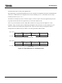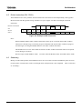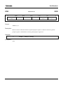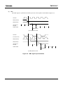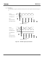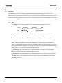
1
32-Bit RISC MICROPROCESSOR TX39 FAMILY CORE ARCHITECTURE USER'S MANUAL Jul. 27, 1995 R3000A is a Trademark of MIPS Technologies, Inc. The information contained herein is subject to change without notice. The information contained herein is presented only as a guide for the applications of our products. No responsibility is assumed by TOSHIBA for any infringements of patents or other rights of the third parties which may result from its use. No license is granted by implication or otherwise under any patent or patent rights of TOSHIBA or others. The products described in this document contain components made in the United States and subject to export control of the U.S.authorities. Diversion contrary to the U.S. law is prohibited. These TOSHIBA products are intended for usage in general electronic equipments (office equipment, communication equipment, measuring equipment, domestic electrification, etc.).Please make sure that you consult with us before you use these TOSHIBA products in equipments which require high quality and/or reliability, and in equipments which could have major impact to the welfare of human life (atomic energy control, airplane, spaceship, traffic signal, combustion control, all type of safety devices, etc.). TOSHIBA cannot accept liability to any damage which may occur in case these TOSHIBA products were used in the mentioned equipments without prior consultation with TOSHIBA, 1995 TOSHIBA CORPORATION All Rights Reserved. CONTENTS CONTENTS Architecture Chapter 1 Introduction--------------------------------------------------------------------------- 3 1.1 Features ------------------------------------------------------------------------------ 3 1.1.1 1.1.2 1.1.3 1.1.4 High-performance RISC techniques ---------------------------------------------------Functions for embedded applications--------------------------------------------------Low power consumption ------------------------------------------------------------------Development environment for embedded arrays and cell-based ICs ---------- 3 3 4 4 1.2 Notation Used in This Manual --------------------------------------------------- 5 Chapter 2 Architecture ------------------------------------------------------------------------- 7 2.1 Overview------------------------------------------------------------------------------ 7 2.2 Registers------------------------------------------------------------------------------ 8 2.2.1 2.2.2 CPU registers--------------------------------------------------------------------------------System control coprocessor (CP0) registers ----------------------------------------- 8 9 2.3 Instruction Set Overview------------------------------------------------------------10 2.4 Data Formats and Addressing ----------------------------------------------------15 2.5 Pipeline Processing Overview-----------------------------------------------------18 2.6 Memory Management Unit (MMU) -----------------------------------------------19 2.6.1 2.6.2 R3900 Processor Core operating modes ----------------------------------------------- 19 Direct segment mapping -------------------------------------------------------------------- 20 Chapter 3 Instruction Set Overview------------------------------------------------------------23 3.1 Instruction Formats ------------------------------------------------------------------23 3.2 Instruction Notation ------------------------------------------------------------------23 3.3 Load and Store Instructions -------------------------------------------------------24 3.4 Computational Instructions---------------------------------------------------------27 3.5 Jump/Branch Instructions ----------------------------------------------------------32 3.6 Special Instructions ------------------------------------------------------------------35 3.7 Coprocessor Instructions -----------------------------------------------------------36 3.8 System Control Coprocessor (CP0) Instructions -----------------------------38 i CONTENTS Chapter 4 Pipeline Architecture-----------------------------------------------------------------39 4.1 Overview--------------------------------------------------------------------------------39 4.2 Delay Slot-------------------------------------------------------------------------------40 4.2.1 4.2.2 Delayed load ----------------------------------------------------------------------------------- 40 Delayed branching---------------------------------------------------------------------------- 40 4.3 Nonblocking Load Function --------------------------------------------------------41 4.4 Multiply and Mupliply/Add Instructions (MULT, MULTU, MADD, MADDU) --41 4.5 Divide Instruction (DIV, DIVU) ----------------------------------------------------42 4.6 Streaming-------------------------------------------------------------------------------42 Chapter 5 Memory Management Unit (MMU) -----------------------------------------------43 5.1 R3900 Processor Core Operating Modes --------------------------------------43 5.2 Direct Segment Mapping -----------------------------------------------------------44 Chapter 6 Exception Processing ---------------------------------------------------------------47 6.1 Overview--------------------------------------------------------------------------------47 6.2 Exception Processing Registers--------------------------------------------------50 6.2.1 6.2.2 6.2.3 6.2.4 6.2.5 6.2.6 6.2.7 6.2.8 6.3 Cause register --------------------------------------------------------------------------------- 51 EPC (Exception Program Counter) register-------------------------------------------- 52 Status register --------------------------------------------------------------------------------- 53 Cache register --------------------------------------------------------------------------------- 56 Status register and Cache register mode bit and exception processing -------- 58 BadVAddr (Bad Virtual Address) register----------------------------------------------- 60 PRId (Processor Revision Identifier) register ------------------------------------------ 60 Config (Configuration) register ------------------------------------------------------------ 61 Exception Details ---------------------------------------------------------------------63 6.3.1 6.3.2 6.3.3 6.3.4 Memory location of exception vectors --------------------------------------------------- 63 Address Error exception -------------------------------------------------------------------- 64 Breakpoint exception------------------------------------------------------------------------- 65 Bus Error exception -------------------------------------------------------------------------- 66 ii CONTENTS 6.3.5 6.3.6 6.3.7 6.3.8 6.3.9 6.3.10 6.3.11 Coprocessor Unusable exception -------------------------------------------------------- 68 Interrupts ---------------------------------------------------------------------------------------- 69 Overflow exception --------------------------------------------------------------------------- 70 Reserved Instruction exception------------------------------------------------------------ 70 Reset exception ------------------------------------------------------------------------------- 71 System Call exception----------------------------------------------------------------------- 72 Non-maskable interrupt --------------------------------------------------------------------- 72 6.4 Priority of Exceptions ----------------------------------------------------------------73 6.5 Return from Exception Handler ---------------------------------------------------73 Chapter 7 Caches ----------------------------------------------------------------------------------75 7.1 Instruction Cache ---------------------------------------------------------------------75 7.2 Data Cache ----------------------------------------------------------------------------76 7.2.1 Lock function ----------------------------------------------------------------------------------- 77 7.3 Cache Test Function-----------------------------------------------------------------79 7.4 Cache Refill ----------------------------------------------------------------------------80 7.5 Cache Snoop --------------------------------------------------------------------------81 Chapter 8 Debugging Functions ----------------------------------------------------------------83 8.1 System Control Processor (CP0) Registers -----------------------------------83 8.2 Debug Exceptions --------------------------------------------------------------------87 8.3 Details of Debug Exceptions-------------------------------------------------------90 Appendix A Instruction Set Details -------------------------------------------------------93 iii CONTENTS TMPR3901F Chapter 1 Introduction--------------------------------------------------------------------------- 201 1.1 Features ------------------------------------------------------------------------------ 201 1.2 Internal Blocks----------------------------------------------------------------------- 203 Chapter 2 Configuration ------------------------------------------------------------------------ 205 2.1 R3900 Processor Core------------------------------------------------------------ 205 2.1.1 2.1.2 Instruction limitations -----------------------------------------------------------------------206 Address mapping ----------------------------------------------------------------------------206 2.2 Clock Generator -------------------------------------------------------------------- 206 2.3 Bus Interface Unit (Bus Controller / Write Buffer)-------------------------- 207 2.4 Memory Protection Unit ----------------------------------------------------------- 208 2.4.1 2.4.2 2.4.3 Registers---------------------------------------------------------------------------------------208 Memory protection exception -------------------------------------------------------------210 Register address map ----------------------------------------------------------------------211 2.5 Debug Support Unit ---------------------------------------------------------------- 211 2.6 Synchronizer ------------------------------------------------------------------------- 211 Chapter 3 Pins ------------------------------------------------------------------------------------ 215 Chapter 4 Operations---------------------------------------------------------------------------- 217 4.1 Clock----------------------------------------------------------------------------------- 217 4.2 Read Operation --------------------------------------------------------------------- 219 4.2.1 4.2.2 Single read ------------------------------------------------------------------------------------219 Burst read--------------------------------------------------------------------------------------221 4.3 Write Operation --------------------------------------------------------------------- 224 4.4 Interrupts------------------------------------------------------------------------------ 225 4.4.1 4.4.2 NMI* ---------------------------------------------------------------------------------------------225 INT[5:0]*----------------------------------------------------------------------------------------226 iv CONTENTS 4.5 Bus Arbitration----------------------------------------------------------------------- 227 4.5.1 4.5.2 Bus request and bus grant-----------------------------------------------------------------227 Cache snoop ----------------------------------------------------------------------------------228 4.6 Reset ---------------------------------------------------------------------------------- 229 4.7 Half-Speed Bus Mode ------------------------------------------------------------- 230 Chapter 5 Power-Down Mode ----------------------------------------------------------------- 231 5.1 Halt mode----------------------------------------------------------------------------- 231 5.2 Standby Mode ----------------------------------------------------------------------- 233 5.3 Doze Mode --------------------------------------------------------------------------- 234 5.4 Reduced Frequency Mode ------------------------------------------------------- 235 v Architecture Architecture 1 Architecture 2 Architecture Chapter 1 Introduction 1.1 Features The R3900 Processor Core is a high-performance 32-bit microprocessor core developed by Toshiba based on the R3000A RISC (Reduced Instruction Set Computer) microprocessor. The R3000A was developed by MIPS Technologies, Inc. Toshiba develops ASSPs (Application Specific Standard Products) using the R3900 Processor Core and provides the R3900 as a processor core in Embedded Array or Cell-based ICs. The low power consumption and high cost-performance ratio of this processor make it especially well-suited to embedded control applications in products such as PDAs (Personal Digital Assistants) and game equipment. 1.1.1 High-performance RISC techniques • R3000A architecture − R3000A upward compatible instruction set (excluding TLB (translation lookaside buffer) instructions and some coprocessor instructions) − Five-stage pipeline • Built-in cache memory − Separate instruction and data caches − Data cache snoop function: Invalidatation of data in the data cache to maintain cache memory and main memory consistency on DMA transfer cycles • Nonblocking load − Execute the following instruction regardless of a cache miss caused by a preceding load instruction • DSP function − Multiply/Add (32-bit x 32-bit + 64-bit) in one clock cycle. 1.1.2 Functions for embedded applications • Small code size − Branch Likely instruction:The branch delay slot accepts an instruction to be executed at the branch target − Hardware Interlock: Stall the pipeline at the load delay slot when the instruction in the slot depends on the data to be loaded 3 Architecture • Real-time performance − Cache Lock Function: Lock one set of the two-way set associative cache memory to keep data in cache memory • Debug support − Breakpoint − Single step execution • Real-time debug system interface 1.1.3 Low power consumption • Power Down mode − Prepare for Reduced Frequency mode: Control the clock frequency of the R3900 Processor Core with a clock generator − Halt and Doze mode: Stop R3900 Processor Core operations • Clock can be stopped − Clock signal can be stopped at high state 1.1.4 Development environment for embedded arrays and cell-based ICs • Compact core • Easy-to-design peripheral circuits − Single direction separate bus: Bus configuration suitable for core − Built-in cache memory: No need to consider cache operation timing • ASIC Process • Sufficient Development Environment 4 Architecture 1.2 Notation Used in This Manual Mathematical notation • Hexadecimal numbers are expressed as follows (example shown for decimal number 42) 0x2A • A K(kilo)byte is 210 = 1,024 bytes, a M(mega)byte is 220 = 1,024 x 1,024 = 1,048,576 bytes, and a G(giga)byte is 230 = 1,024 x 1,024 x 1,024 = 1,073,741,824 bytes. Data notation • Byte: 8 bits • Halfword: 2 contiguous bytes (16 bits) • Word: 4 contiguous bytes (32 bits) • Doubleword: 8 contiguous bytes (64 bits) Signal notation • Low active signals are indicated by an asterisk (*) at the end of the signal name (e.g.: RESET*). • Changing a signal to active level is to “assert” a signal, while changing it to a non-active level is to “deassert” the signal. 5 Architecture 2. 6 Architecture Chapter 2 Architecture 2.1 Overview A block diagram of the R3900 Processor Core is shown in Figure 2-1. It includes the CPU core, an instruction cache and a data cache. You can select an optimum data and instruction cache configuration for your system from among a variety of possible configurations. The CPU Core comprises the following blocks: • CPU registers : General-purpose register, HI/LO register and program counter (PC). • CP0 registers : Registers for system control coprocessor (CP0) functions. • ALU/Shifter : Computational unit. • MAC : Computational unit for multiply/add. • Bus interface unit : Control bus interface between CPU core and external circuit. • Memory management unit : Direct segment mapping memory management unit. R3900 Processor Core CPU core CPU Register CP0 Register ALU/Shifter Memory Management Unit MAC Bus Interface Unit Instruction Cache Data Cache Figure 2-1. Block Diagram of the R3900 Processor Core 7 Architecture 2.2 Registers 2.2.1 CPU registers The R3900 Processor Core has the following 32-bit registers. • Thirty-two general-purpose registers • A program counter (PC) • HI/LO registers for storing the result of multiply and divide operations The configuration of the registers is shown in Figure 2-2. Multiply/Divide registers General-purpose registers 31 0 31 0 r0 HI r1 31 0 r2 LO . . . . Program counter r29 31 0 PC r30 r31 Figure 2-2. R3900 Processor Core registers The r0 and r31 registers have special functions. • Register r0 always contains the value 0. It can be a target register of an instruction whose operation result is not needed. Or, it can be a source register of an instruction that requires a value of 0. • Register r31 is the link register for the Jump And Link instruction. The address of the instruction after the delay slot is placed in r31. The R3900 Processor Core has the following three special registers that are used or modified implicitly by certain instructions. PC : Program counter HI : High word of the multiply/divide registers LO : Low word of the multiply/divide registers The multiply/divide registers (HI, LO) store the double-word (64-bit) result of integer multiply operations. In the case of integer divide operations, the quotient is stored in LO and the remainder in HI. 8 Architecture 2.2.2 System control coprocessor (CP0) registers The R3900 Processor Core can be connected to as many as three coprocessors, referred to as CP1, CP2 and CP3. The R3900 also has built-in system control coprocessor (CP0) functions for exception handling and for configuring the system. Figure 2-3 shows the functional breakdown of the CP0 registers. <Exception Processing> Status register Cause register EPC register BadVAddr register PRld register Config register† † Cache register† Additional R3900 Processor Core registers not present in the R3000A <Debugging> Debug register† DEPC register† Figure 2-3 CP0 registers 9 Architecture Table 2-1 lists the CP0 registers built into the R3900 Processor Core. Some of these registers are reserved for use by an external memory management unit. Table 2-1. List of system control coprocessor (CP0) registers No Mnemonic Description - (reserved) † - (reserved) † - (reserved) † 0 1 2 Config†† Hardware configuration 3 - (reserved) † - (reserved) † - (reserved) † 4 5 6 Cache†† Cache lock function BadVAddr Last virtual address triggering error 7 8 9 10 11 12 13 14 15 16 17 18 | 31 † †† ††† - (reserved) † - (reserved) † (reserved) † Information on mode, interrupt enabled, diagnostic status Indicates nature of last exception Exception program counter Processor revision ID Debug exception control Program counter for debug exception (reserved) † Status Cause EPC PRId Debug††† DEPC††† - Reserved for external memory management unit, when direct segment mapping MMU is not used. Additional R3900 Processor Core register not present in R3000A. Additional R3900 Processor Core Debug register not present in R3000A. 10 Architecture 2.3 Instruction Set Overview All R3900 Processor Core instructions are 32 bits in length. There are three instruction formats: immediate (I-type), jump (J-type) and register (R-type), as shown in Figure 2-4. Having just three instruction formats simplifies instruction decoding. If more complex functions or addressing modes are required, they can be produced with the compiler using combinations of the instructions. I-type (Immediate) 31 26 25 op 21 20 rs 16 15 0 rt immediate J-type (Jump) 31 26 25 0 op target R-type (Register) 31 26 25 op op rs rt rd immediate target sa funct 21 20 rs 16 15 rt 11 10 rd 6 5 sa 0 funct Operation code (6 bits) Source register (5 bits) Target (source or destination) register, or branch condition (5 bits) Destination register (5 bits) Immediate, branch displacement, address displacement (16 bits) Branch target address (26 bits) Shift amount (5 bits) Function (6 bits) Figure 2-4. Instruction formats and subfield mnemonics 11 Architecture The instruction set is classified as follows. (1) Load/store These instructions transfer data between memory and general registers. All instructions in this group are I-type. “Base register + 16 bit signed immediate offset” is the only supported addressing mode. (2) Computational These instructions perform arithmetic, logical and shift operations on register values. The format can be R-type (when both operands and the result are register values) or I-type (when one operand is 16bit immediate data). (3) Jump/branch These instructions change the program flow. A jump is always made to a 32 bit address contained in a register (R-type format ), or to a paged absolute address constructed by combining a 26-bit target address with the upper 4 bits of the program counter (J-type format). In a branch instruction, the target address is made up of the program counter value plus a 16 bit offset. (4) Coprocessor These instructions execute coprocessor operations. Each coprocessor has its own format for computational instructions. Note : Coprocessor load instruction LWCz and coprocessor store instruction SWCz are not supported by the R3900 Processor Core. An attempt to execute either of these instructions will trigger a Reserved Instruction exception. (5) Coprocessor 0 These instructions are used for operations with system control coprocessor (CP0) registers, processor memory management and exception handling. Note : TLB (Translation Lookaside Buffer) instructions (TLBR, TLBWJ, TLBWR and TLBP) are not supported by the R3900 Processor Core. These instructions will be treated by the R3900 as NOP(no operation). (6) Special These instructions support system calls and breakpoint functions. The format is always R-type. 12 Architecture The instruction set supported by all MIPS R-Series processors is listed in Table 2-2. Table 2-3 shows extended instructions supported by the R3900 Processor Core, and Table 2-4 lists coprocessor 0 (CP0) instructions. Table 2-5 shows R3000A instructions not supported by the R3900 Processor Core. Table 2-2. Instructions supported by MIPS R-Series processors (ISA) Instruction Description Load/Store Instructions LB Load Byte LBU Load Byte Unsigned LH Load Halfword LHU Load Halfword Unsigned LW Load Word LWL Load Word Left LWR Load Word Right SB Store Byte SH Store Halfword SW Store Word SWL Store Word Left SWR Store Word Right Computational Instructions (ALU Immediate) ADDI Add Immediate ADDIU Add Immediate Unsigned SLTI Set on Less Than Immediate SLTIU Set on Less Than Immediate Unsigned ANDI AND Immediate ORI OR Immediate XORI XOR Immediate LUI Load Upper Immediate (ALU 3-operand, register type) ADD Add ADDU Add Unsigned SUB Subtract SUBU Subtract Unsigned SLT Set on Less Than SLTU Set on Less Than Unsigned AND AND OR OR XOR XOR NOR NOR 13 Architecture Table 2-2(cont.). Instructions supported by MIPS R-Series processors (ISA) Instruction Description (Shift) SLL Shift Left Logical SRL Shift Right Logical SRA Shift Right Arithmetic SLLV Shift Left Logical Variable SRLV Shift Right Logical Variable SRAV Shift Right Arithmetic Variable (Multiply/Divide) MULT Multiply MULTU Multiply Unsigned DIV Divide DIVU Divide Unsigned MFHI Move from HI MTHI Move to HI MFLO Move from LO MTLO Move to LO Jump/Branch Instructions J Jump JAL Jump And Link JR Jump Register JALR Jump And Link Register BEQ Branch on Equal BNE Branch on Not Equal BLEZ Branch on Less than or Equal to Zero BGTZ Branch on Greater Than Zero BLTZ Branch on Less Than Zero BGEZ Branch on Greater than or Equal to Zero BLTZAL Branch on Less Than Zero And Link BGEZAL Branch on Greater than or Equal to Zero And Link Coprocessor Instructions MTCz Move to Coprocessor z MFCz Move from Coprocessor z CTCz Move Control Word to Coprocessor z CFCz Move control Word from Coprocessor z COPz Coprocessor Operation z BCzT Branch on Coprocessor z True BCzF Branch on Coprocessor z False Special Instructions SYSCALL System Call BREAK Breakpoint 14 Architecture Table 2-3. R3900 extended instructions Instruction Description Load/Store Instruction SYNC Sync Computational Instructions MULT Multiply (3-operand instruction) MULTU Multiply Unsigned (3-operand instruction) MADD Multiply/ADD MADDU Multiply/ADD Unsigned Jump/Branch Instructions BEQL Branch on Equal Likely BNEL Branch on Not Equal Likely BLEZL Branch on Less than or Equal to Zero Likely BGTZL Branch on Greater Than Zero Likely BLTZL Branch on Less Than Zero Likely BGEZL Branch on Greater than or Equal to Zero Likely BLTZALL Branch on Less Than Zero And Link Likely BGEZALL Branch on Greater than or Equal to Zero And Link Likely Coprocessor Instructions BCzTL Branch on Coprocessor z True Likely BCzFL Branch on Coprocessor z False Likely Special Instruction SDBBP Software Debug Breakpoint Table 2-4. CP0 instructions Instruction CP0 Instructions MTC0 MFC0 RFE DERET CACHE Description Move to CP0 Move from CP0 Restore from Exception Debug Exception Return Cache Operation Table 2-5. R3000A instructions not supported by the R3900 Instruction Description Operation Coprocessor Instructions LWCz Load Word from Coprocessor SWCz Store Word to Coprocessor CP0 Instructions TLBR Read indexed TLB entry TLBWJ Write indexed TLB entry TLBWR Write Random TLB entry TLBP Probe TLB for matching entry 15 Reserved Instruction Exception Reserved Instruction Exception no operation(nop) no operation(nop) no operation(nop) no operation(nop) Architecture 2.4 Data Formats and Addressing This section explains how data is organized in R3900 registers and memory. The R3900 uses the following data formats: 64-bit doubleword, 32-bit word, 16-bit halfword and 8-bit byte. The byte order can be set to either big endian or little endian. Figure 2-5 shows how bytes are ordered in words, and how words are ordered in multiple words, for both the big-endian and little-endian formats. Higher address 31 23 16 15 87 24 Lower address Word address 0 8 9 10 11 8 4 5 6 7 4 0 1 2 3 0 Byte 0 is the most significant byte (bit 31-24). A word is addressed beginning with the most significant byte. (a) Big endian Higher address Lower address 31 23 15 7 24 16 8 0 Word address 11 10 9 8 8 7 6 5 4 4 3 2 1 0 0 Byte 0 is the least significant byte (bit 7-0). A word is addressed beginning with the least significant byte. (b) Little endian Figure 2-5. Big endian and little endian formats 16 Architecture 17 Architecture In this document (bit 0 is always the rightmost bit). Byte addressing is used with the R3900 Processor Core, but there are alignment restrictions for halfword and word access. Halfword access is aligned on an even byte boundary (0, 2, 4...) and word access on a byte boundary divisible by 4 (0, 4, 8...) . The address of multiple-byte data, as shown in Figure 2-5 above, begins at the most significant byte for the big endian format and at the least significant byte for the little endian format. There are special instructions (LWL, LWR, SWL, SWR) for accessing words not aligned on a word boundary. They are used in pairs for addressing misaligned words, but involve an extra instruction cycle which is wasted if used with properly aligned words. Figure 2-6 shows the byte arrangement when a misaligned word is addressed at byte address 3 for the big and little endian formats. Higher address 31 24 23 4 16 15 5 87 0 6 3 Lower address (a) Big endian Higher address 31 24 23 16 15 6 87 5 0 4 3 Lower address (b)Little endian Figure 2-6. Byte addresses of a misaligned word 18 Architecture 2.5 Pipeline Processing Overview The R3900 Processor Core executes instructions in five pipeline stages (F: instruction fetch; D: decode; E: execute; M: memory access; W: register write-back). Each pipeline stage is executed in one clock cycle. When the pipeline is fully utilized, five instructions are executed at the same time resulting in an instruction execution rate of one instruction per cycle. With the R3900 Processor Core an instruction that immediately follows a load instruction can use the result of that load instruction. Execution of the following instruction is delayed by hardware interlock until the result of the load instruction becomes available. The instruction position immediately following the load instruction is called the “load delay slot.” In the case of branch instructions, a one-cycle delay is required to generate the branch target address. This delayed cycle is referred to as the “branch delay slot.” An instruction placed immediately after a branch instruction (in the branch delay slot) can be executed prior to the branch while the branch target address is being generated. The R3900 Processor Core provides a Branch Likely instruction whereby an instruction to be executed at the branch target can be placed in the delay slot of the Branch Likely instruction and executed only if the conditions of the branch instruction are met. If the conditions are not met, and the branch is not taken, the instruction in the delay slot is treated as a NOP. This makes it possible to place an instruction that would normally be executed at the branch target into the delay slot for quick execution (if the conditions of the branch are met). F D E M W F D E M W F D E M W F D E M W F D E M W Current CPU cycle Figure 2-7. Pipeline stages for execution of R3900 Processor Core instructions 19 Architecture 2.6 Memory Management Unit (MMU) 2.6.1 R3900 Processor Core operating modes The R3900 Processor Core has two operating modes, user mode and kernel mode. Normally the processor operates in user mode. It switches to kernel mode if an exception is detected. Once in kernel mode, it remains there until an RFE (Restore From Exception) instruction is executed. (1) User mode User mode makes available one of the two 2 Gbyte virtual address spaces (kuseg). In this mode the most significant bit of each kuseg address in the memory map is 0. Attempting to access an address whose MSB is 1 while in user mode returns an Address Error exception. (2) Kernel mode Kernel mode makes available a second 2 Gbyte virtual address space (kseg), in addition to the kuseg accessible in user mode. The MSB of each kseg address in the memory map is 1. 20 Architecture 2.6.2 Direct segment mapping The R3900 Processor Core includes a direct segment mapping MMU. The following virtual address spaces are available depending on the processor mode (Figure 2-8 shows the address mapping). (1) User mode One 2 Gbyte virtual address space (kuseg) is available. Virtual addresses from 0x0000 0000 to 0x7FFF FFFF are translated to physical addresses 0x4000 0000 to 0xBFFF FFFF, respectively. (2) Kernel mode The kernel mode address space is treated as four virtual address segments. One of these is the same as the kuseg space in user mode; the remaining three are the kernel segments kseg0, kseg1 and kseg2. (a) kuseg This is the same as the virtual address space available in user mode. Address translation is also the same as in user mode. The upper 16 Mbytes of kuseg is reserved for on-chip resources and is not cacheable. (b) kseg0 This is a 512 Mbyte segment spanning virtual addresses 0x8000 0000 to 0x9FFF FFFF. Fixed mapping of this segment is made to physical addresses 0x0000 0000 to 0x1FFF FFFF, respectively. (c) This area is cacheable. kseg1 This is a 512 Mbyte segment from virtual address 0xA000 0000 to 0xBFFF FFFF. Fixed mapping of this segment is made to physical address 0x0000 0000 to 0x1FFF FFFF, respectively. Unlike kseg0, this area is not cacheable. (d) kseg2 This is a 1 Gbyte linear address space from virtual addresses 0xC000 0000 to 0xFFFF FFFF. The upper 16 Mbytes of kseg2 are reserved for on-chip resources and are not cacheable. Of this reserved area, 0xFF20 0000 to 0xFF3F FFFF is a 2 Mbyte reserved area intended for use as a debugging monitor area and for testing. 21 Architecture Virtual address space Physical address space 0xFFFF FFFF 16MB Kernel Reserved Kernel Cached Tasks Kernel Cached 0xC000 0000 1024MB (kseg2) Kernel Uncached 0xA000 0000 (kseg1) Kernel/User Kernel Cached 0x8000 0000 2048MB Cached Tasks (kseg0) 16MB User Reserved Inaccessible 512MB Kernel/User Cached (kuseg) Kernel Boot and I/O 0x0000 0000 Cached/uncached Figure 2-8. Address mapping 22 512MB Architecture 3. 22 Architecture Chapter 3 Instruction Set Overview This chapter summarizes each of the R3900 Processor Core instruction types in table format and explains each instruction briefly. Details of individual instructions are given in Appendix A. 3.1 Instruction Formats Each of the R3900 Processor Core instructions is aligned on a word boundary and has a 32-bit (single-word) length. There are only three instruction formats, as shown in Figure 3-1. As a result, instruction decoding is simplified. Less frequently used and more complex functions or addressing modes can be realized by combining these instructions. I-type (Immediate) 31 26 25 op 21 20 rs 16 15 0 rt immediate J-type (Jump) 31 26 25 0 op target R-type (Register) 31 26 25 op op rs rt rd immediate target sa funct 21 20 rs 16 15 rt 11 10 rd 65 sa 0 funct Operation code (6 bits) Source register (5 bits) Target (source or destination) register, or branch condition (5 bits) Destination register (5 bits) Immediate, branch displacement, address displacement (16 bits) Branch target address (26 bits) Shift amount (5 bits) Function (6 bits) Figure 3-1. Instruction Formats and subfield mnemonics 3.2 Instruction Notation All variable subfields in the instruction formats used here are written in lower-case letters (rs, rt, immediate, etc.). Also, an alias is sometimes used for a subfield name, for the sake of clarity. For example, rs in a load/store instruction may be referred to as “base”. When such an alias refers to a subfield that can take a variable value, it is likewise written in lower-case letters. With specific instructions, the instruction subfields “op” and “funct” have fixed 6-bit values. These values are thus written as equates in upper-case letters. In the Load Byte instruction, for example, op = LB; and in the ADD instruction, op = SPECIAL and function = ADD. 23 Architecture 3.3 Load and Store Instructions Load and Store instructions move data between memory and general registers and are all I-type instructions. The only directly supported addressing mode is base register plus 16-bit signed immediate offset. With the R3900 Processor Core, the result of a load instruction can be used by the immediately following instruction. Execution of the following instruction is delayed by hardware interlock until the load result becomes available. The instruction position immediately following the load instruction is referred to as the load delay slot . In the case of the LWL (Load Word Left) and LWR (Load Word Right) instructions, however, it is possible to use the destination register of an immediately preceding load instruction as the target register of the LWL or LWR instruction. The access type, which indicates the size of data to be loaded or stored, is determined by the operation code (op) of the load or store instruction. The target address of a load or store is always the smallest byte address of the target data byte string, regardless of the access type or endian. This address is the most significant byte for the big endian format, and the least significant byte for the little endian format. The position of the accessed data is determined by the access type and the two low-order address bits, as shown in Table 3-1. Designating a combination other than those shown in table 3-1 results in an Address Error exception. Table 3-1. Byte specifications for load and store instructions Low order Access Type Accessed Bytes address bits Big Endian 1 0 31 word 0 0 0 1 2 triple-byte 0 0 0 1 2 0 1 1 2 0 0 1 0 0 0 0 1 1 0 1 1 halfword byte 0 Little Endian 0 31 3 3 3 3 0 2 1 0 2 1 0 2 1 1 1 2 3 3 0 2 0 0 1 1 2 2 3 24 3 Architecture Table 3-2. Load/store instructions (1/2) Instruction Format and Description Load Byte LB rt, offset (base) Generate the address by sign-extending a 32-bit offset and adding it to the contents of register base. Sign-extend the contents of the addressed byte and load into register rt. LBU rt, offset (base) Generate the address by sign-extending a 32-bit offset and adding it to the contents of register base. Zero-extend the contents of the addressed byte and load into register rt. LH rt, offset (base) Generate the address by sign-extending a 32-bit offset and adding it to the contents of register base. Sign-extend the contents of the addressed halfword and load into register rt. LHU rt, offset (base) Generate the address by sign-extending a 32-bit offset and adding it to the contents of register base. Zero-extend the contents of the addressed halfword and load into register rt. LW rt, offset (base) Generate the address by sign-extending a 32-bit offset and adding it to the contents of register base. Load the contents of the addressed word into register rt. LWL rt, offset (base) Generate the address by sign-extending a 32-bit offset and adding it to the contents of register base. This instruction is paired with LWR and used to load word data not aligned with a word boundary. The LWL instruction loads the left part of the word, and LWR loads the right part. LWL shifts the addressed byte to the left, so that it will form the left side of the word, merges it with the contents of register rt and loads the result into rt. LWR rt, offset (base) Generate the address by sign-extending a 32-bit offset and adding it to the contents of register base. LWR shifts the addressed byte to the right, so that it will form the right side of the word, merges it with the contents of register rt and loads the result into rt. SB rt, offset (base) Generate the address by sign-extending a 32-bit offset and adding it to the contents of register base. Store the contents of the least significant byte of register rt at the addressed byte. SH rt, offset (base) Generate the address by sign-extending a 32-bit offset and adding it to the contents of register base. Store the contents of the least significant halfword of register rt at the addressed byte. Load Byte Unsigned Load Halfword Load Halfword Unsigned Load Word Load Word Left Load Word Right Store Byte Store Halfword op 25 base rt offset Architecture Table 3-2. Load/store instructions (2/2) Instruction Format and Description Store Word SW rt, offset (base) Generate the address by sign-extending a 32-bit offset and adding it to the contents of register base. Store the contents of the least significant word of register rt at the addressed byte. SWL rt, offset (base) Generate the address by sign-extending a 32-bit offset and adding it to the contents of register base. This instruction is used together with SWR to store the contents of a register into four consecutive bytes of memory when the bytes cross a word boundary. The SWL instruction stores the left part of the register, and SWR stores the right part. SWL shifts the contents of register rt to the right so that the leftmost byte of the word aligns with the addressed byte. It then stores the bytes containing the original data in the corresponding bytes at the addressed byte. SWR rt, offset (base) Generate the address by sign-extending a 32-bit offset and adding it to the contents of register base. SWR shifts the contents of register rt to the left so that the rightmost byte of the word aligns with the addressed byte. It then stores the bytes containing the original data in the corresponding bytes at the addressed byte. Store Word Left Store Word Right op base rt offset Table 3-3. Load/store instructions (R3000A extended set) Instruction Format and Description SYNC SYNC Interlock the pipeline while a load or store instruction is executing, until execution is completed. op 26 0 funct Architecture 3.4 Computational Instructions Computational instructions perform arithmetic, logical or shift operations on values in registers. The instruction format can be R-type or I-type. With R-type instructions, the two operands and the result are register values. With I-type instructions, one of the operands is 16-bit immediate data. Computational instructions can be classified as follows. • ALU immediate (Table 3-4) • Three-operand register-type (Table 3-5) • Shift (Table 3-6) • Multiply/Divide (Table 3-7,Table3-8) Table 3-4. ALU immediate instructions Instruction Format and Description Add Immediate ADDI rt, rs, immediate Add 32-bit sign-extended immediate to the contents of register rs, and store the result in register rt. An exception is raised in the event of a two’s-complement overflow. ADDIU rt, rs, immediate Add 32-bit sign-extended immediate to the contents of register rs, and store the result in register rt. No exception is raised on a two’s-complement overflow. SLTI rt, rs, immediate Compare 32-bit sign-extended immediate with the contents of register rs as signed 32-bit data. If rs is less than immediate, set 1 in rt as the result; otherwise store 0 in rt. SLTUI rt, rs, immediate Compare 32-bit sign-extended immediate with the contents of register rs as unsigned 32-bit data. If rs is less than immediate, set 1 in rt as the result; otherwise store 0 in rt. ANDI rt, rs, immediate AND 32-bit zero-extended immediate with the contents of register rs, and store the result in register rt. ORI rt, rs, immediate OR 32-bit zero-extended immediate with the contents of register rs, and store the result in register rt. XORI rt, rs, immediate Exclusive-OR 32-bit zero-extended immediate with the contents of register rs, and store the result in register rt. LUI rt, immediate Shift 16-bit immediate left 16 bits, zero-fill the least significant 16 bits of the word, and store the result in register rt. Add Immediate Unsigned Set on Less Than Immediate Set on Less Than Unsigned Immediate AND Immediate OR Immediate Exclusive OR Immediate Load Upper Immediate op 27 rs rt immediate Architecture Table 3-5. Three-operand register-type instructions Instruction Format and Description op Add rs rt rd 0 funct ADD rd, rs, rt Add the contents of registers rs and rt, and store the result in register rd. An exception is raised in the event of a two’s-complement overflow. Add Unsigned ADDU rd, rs, rt Add the contents of registers rs and rt, and store the result in register rd. No exception is raised on a two’s-complement overflow. Subtract SUB rd, rs, rt Subtract the contents of register rt from rs, and store the result in register rd. An exception is raised in the event of a two’s-complement overflow. Subtract SUBU rd, rs, rt Unsigned Subtract the contents of register rt from rs, and store the result in register rd. No exception is raised on a two’s-complement overflow. Set on Less SLT rd, rs, rt Than Compare the contents of registers rt and rs as 32-bit signed integers. If rs is less than rt, store 1 in rd as the result; otherwise store 0 in rd. Set on Less SLTU rd, rs, rt Than Unsigned Compare the contents of registers rt and rs as 32-bit unsigned integers. If rs is less than rt, store 1 in rd as the result; otherwise store 0 in rd. AND AND rd, rs, rt Bitwise AND the contents of registers rs and rt, and store the result in register rd. OR OR rd, rs, rt Bitwise OR the contents of registers rs and rt, and store the result in register rd. Exclusive OR XOR rd, rs, rt Bitwise Exclusive-OR the contents of registers rs and rt, and store the result in register rd. NOR NOR rd, rs, rt Bitwise NOR the contents of registers rs and rt, and store the result in register rd. 28 Architecture Table 3-6. Shift instructions (a) SLL, SRL, SRA Instruction Format and Description Shift Left Logical SLL rd, rt, sa Left-shift the contents of register rt by the number of bits indicated in sa (shift amount), and zero-fill the low-order bits. Store the resulting 32 bits in register rd. SRL rd, rt, sa Right-shift the contents of register rt by sa bits, and zero-fill the high-order bits. Store the resulting 32 bits in register rd. SRA rd, rt, sa Right-shift the contents of register rt by sa bits, and sign-extend the high-order bits. Store the resulting 32 bits in register rd. Shift Right Logical Shift Right Arithmetic op 0 rt rd sa funct (b) SLLV, SRLV, SRAV Instruction Format and Description Shift Left Logical Variable SLLV rd, rt, sa Left-shift the contents of register rt. The number of bits shifted is indicated in the 5 low-order bits of the register rs contents. Zero-fill the low-order bits of rt and store the resulting 32 bits in register rd. SRLV rd, rt, sa Right-shift the contents of register rt. The number of bits shifted is indicated in the 5 low-order bits of the register rs contents. Zero-fill the high-order bits of rt and store the resulting 32 bits in register rd. SRAV rd, rt, sa Right-shift the contents of register rt. The number of bits shifted is indicated in the 5 low-order bits of the register rs contents. Sign-extend the high-order bits of rt and store the resulting 32 bits in register rd. Shift Right Logical Variable Shift Right Arithmetic Variable op 29 rs rt rd 0 funct Architecture Table 3-7. Multiply/Divide Instructions (a) MULT, MULTU, DIV, DIVU Instruction Format and Description Multiply MULT rs, rt Multiply the contents of registers rs and rt as two's complement integers, and store the doubleword (64-bit) result in multiply/divide registers HI and LO. MULTU rs, rt Multiply the contents of registers rs and rt as unsigned integers, and store the doubleword (64-bit) result in multiply/divide registers HI and LO. DIV rs, rt Divide register rs by register rt as two's complement integers. Store the 32-bit quotient in LO, and the 32-bit remainder in HI. DIVU rs, rt Divide register rs by register rt as unsigned integers. Store the 32-bit quotient in LO, and the 32-bit remainder in HI. Multiply Unsigned Divide Divide Unsigned op rs rt 0 funct (b) MFHI, MFLO Instruction Format and Description op 0 rd 0 funct Move From HI MFHI rd Store the contents of multiply/divide register HI in register rd. Move From MFLO rd LO Store the contents of multiply/divide register LO in register rd. (c) MTHI, MTLO Instruction Format and Description Move To HI MTHI rs Store the contents of register rs in multiply/divide register HI. MTLO rs Store the contents of register rs in multiply/divide register LO. Move To LO op 30 rs 0 funct Architecture Table 3-8. Multiply, multiply / add instructions (R3000A extended instruction set) MULT, MULTU, MADD, MADDU (ISA extended set) Instruction Format and Description Multiply MULT rd, rs, rt Multiply the contents of registers rs and rt as two’s complement integers, and store the doubleword (64-bit) result in multiply/divide registers HI and LO. Also, store the lower 32 bits in register rd. MULTU rd, rs, rt Multiply the contents of registers rs and rt as unsigned integers, and store the doubleword (64-bit) result in multiply/divide registers HI and LO. Also, store the lower 32 bits in register rd. MADD rd, rs, rt MADD rs, rt Multiply the contents of registers rs and rt as two’s complement integers, and add the doubleword (64-bit) result to multiply/divide registers HI and LO. Also, store the lower 32 bits of the add result in register rd. In the MADD rs, rt format, the store operation to a general register is omitted. MADDU rd, rs, rt MADDU rs, rt Multiply the contents of registers rs and rt as unsigned integers, and add the doubleword (64-bit) result to multiply/divide registers HI and LO. Also, store the lower 32 bits of the add result in register rd. In the MADDU rs, rt format, the store operation to a general register is omitted. Multiply Unsigned Multiply ADD Multiply ADD Unsigned op 31 rs rt rd 0 funct Architecture 3.5 Jump/Branch Instructions Jump/branch instructions change the program flow. A jump/branch instruction will delay the pipeline by one instruction cycle, however, an instruction inserted into the delay slot (immediately following a branch instruction) can be executed while the instruction at the branch target address is being fetched. Jump and Jump And Link instructions, typically used to call subroutines, have the J-type instruction format. The jump target address is generated as follows. The 26-bit target address (target) of the instruction is leftshifted two bits and combined with the high-order four bits of the current PC (program counter) value to form a 32-bit absolute address. This becomes the branch target address of the jump instruction. The PC shows the address of the branch delay slot at that time. The Jump And Link instruction puts the return address in register r31. The R-type instruction format is used for returns from subroutines and long-distance jumps beyond one page (Jump Register and Jump And Link Register instructions). The register value in this format is a 32-bit byte address. Branch instructions use the I-type format. Branching is to an relative address determined by adding a 16-bit signed offset to the program counter. Table 3-9. Jump instructions (a) J, JAL Instruction Format and Description Jump J target Left-shift the 26-bit target by two bits and, after a one-instruction delay, jump to an address formed by combining this result with the high-order 4 bits of the program counter (PC). JAL target Left-shift the 26-bit target by two bits and, after a one-instruction delay, jump to an address formed by combining the result with the high-order 4 bits of the program counter (PC). Store in r31 (link register) the address of the instruction following the instruction in the delay slot (The instruction in the delay slot is executed during the jump). Jump And Link op target (b) JR Instruction Format and Description Jump Register JR rs Jump to the address in register rs after a one-instruction delay. op rs 0 funct (c) JALR Instruction Format and Description Jump And Link Register JALR rs, rd Jump to the address in register rs after a one-instruction delay. Store in rd the address of the instruction following the instruction in the delay slot (the op 32 rd 0 rd 0 funct Architecture instruction in the delay slot is executed during the jump). The following notes apply to Table 3-10. • The target address of a branch instruction is generated by adding the address of the instruction in the delay slot (the instruction to be executed during the branch) to the 16-bit offset (that has been left-shifted two bits and sign-extended to 32 bits). Branch instructions are executed with a one-cycle delay. • In the case of the Branch Likely instructions in Table 3-10, if the branch condition is not met and the branch is not taken, the instruction in the delay slot is treated as a NOP. Table 3-10. Branch instructions (a) BEQ, BNE Instruction Format and Description Branch on Equal Branch on Not Equal BEQ rs, rt, offset Branch to the target if the contents of registers rs and rt are equal. BNE rs, rt, offset Branch to the target if the contents of registers rs and rt are not equal. op rs rt offset (b) BLEZ, BGTZ Instruction Format and Description Branch on Less Than or Equal Zero Branch on Greater Than Zero BLEZ rs, offset Branch to the target if register rs is 0 or less. op rs 0 offset funct offset BGTZ rs, offset Branch to the target if register rs is greater than 0. (c) BLTZ, BGEZ, BLTZAL, BGEZAL Instruction Format and Description Branch on Less Than Zero Branch on Greater Than or Equal Zero Branch on Less Than Zero And Link BLTZ rs, offset Branch to the target if register rs is less than zero Branch on Greater Than or Equal Zero And Link op rs BGEZ rs, offset Branch to the target if register rs is 0 or greater. BLTZAL rs, offset Store in r31 (link register) the address of the instruction following the instruction in the delay slot (the one to be executed during the branch). If register rs is less than 0, branch to the target. BGEZAL rs, offset Store in r31 (link register) the address of the instruction following the instruction in the delay slot (the instruction in the delay slot is executed during the branch). If register rs is 0 or greater, branch to the target. 33 Architecture (d) BEQL, BNEL, BLEZL, BGTZL, BLTZL, BGEZL, BLTZALL, BGEZALL (ISA Extended Set) Instruction Format and Description Branch on Equal Likely Branch on Not Equal Likely Branch on Less Than or Equal Zero Likely Branch on Greater Than Zero Likely BEQL rs, rt, offset Branch to the target if the contents of registers rs and rt are equal. BNEL rs, rt, offset Branch to the target if the contents of registers rs and rt are not equal. BLEZL rs, offset Branch to the target if register rs is 0 or less. Instruction Format and Description Branch on Less Than Zero Likely Branch on Greater Than or Equal Zero Likely Branch on Less Than Zero And Link Likely Branch on Greater Than or Equal Zero And Link Likely BLTZL rs, offset Branch to the target if register rs is less than zero op rs rt offset BGTZL rs, offset Branch to the target if register rs is greater than 0. op rs funct offset BGEZL rs, offset Branch to the target if register rs is 0 or greater. BLTZALL rs, offset Store in r31 (link register) the address of the instruction following the instruction in the delay slot (the one to be executed during the branch). If register rs is less than 0, branch to the target. BGEZALL rs, offset Store in r31 (link register) the address of the instruction following the instruction in the delay slot (the instruction in the delay slot is executed during the branch). If register rs is 0 or greater, branch to the target. 34 Architecture 3.6 Special Instructions There are three special instructions used for software traps. The instruction format is R-type for all three. Table 3-11. Special instructions (a) SYSCALL Instruction Format and Description System Call SYSCALL code Raise a system call exception, passing control to an exception handler. op code funct (b) BREAK Instruction Format and Description Breakpoint BREAK code Raise a breakpoint exception, passing control to an exception handler. op code funct (c) SDBBP Instruction Format and Description Software Debug Breakpoint SDBBP code Raise a debug exception, passing control to an exception processor. op 35 code funct Architecture 3.7 Coprocessor Instructions Coprocessor instructions invoke coprocessor operations. The format of these instructions depends on which coprocessor is used. Table 3-12. Coprocessor instructions (a) MTCz, MFCz, CTCz, CFCz Instruction Format and Description Move To Coprocessor MTCz rt, rd Move the contents of CPU general register rt to coprocessor z’s coprocessor register rd. MFCz rt, rd Move the contents of coprocessor z’s coprocessor register rd to CPU general register rt. CTCz rt, rd Move the contents of CPU general register rt to coprocessor z’s coprocessor control register rd. CFCz rt, rd Move the contents of coprocessor z’s coprocessor control register rd to CPU general register rt. Move From Coprocessor Move Control To Coprocessor Move Control From Coprocessor op funct rt rd 0 (b) COPz Instruction Format and Description Coprocessor Operation COPz cofun Execute in coprocessor z the processing indicated in cofun. The CPU state is not changed by the processing executed in the coprocessor. op co cofun (c) BCzT, BCzF Instruction Format and Description Branch on Coprocessor z True BCzT offset Generate the branch target address by adding the address of the instruction in the delay slot (the instruction to be executed during the branch) and the 16-bit offset (after left-shifting two bits and sign-extending to 32 bits). If the coprocessor z condition line is true, branch to the target address after a onecycle delay. BCzF offset Generate the branch target address by adding the address of the instruction in the delay slot (the instruction to be executed during the branch) and the 16-bit offset (after left-shifting two bits and sign-extending to 32 bits). If the coprocessor z condition line is false, branch to the target address after a onecycle delay. Branch on Coprocessor z False op 36 funct offset Architecture (d) BCzTL, BCzFL (ISA Extended Set) Instruction Format and Description Branch on Coprocessor z True Likely BCzTL offset Generate the branch target address by adding the address of the instruction in the delay slot (the instruction to be executed during the branch) and the 16-bit offset (after left-shifting two bits and sign-extending to 32 bits). If the coprocessor z condition line is true, branch to the target address after a onecycle delay. If the condition line is false, nullify the instruction in the delay slot. BCzFL offset Generate the branch target address by adding the address of the instruction in the delay slot (the instruction to be executed during the branch) and the 16-bit offset (after left-shifting two bits and sign-extending to 32 bits). If the coprocessor z condition line is false, branch to the target address after a onecycle delay. If the condition line is true, nullify the instruction in the delay slot. Branch on Coprocessor z False Likely op 37 funct offset Architecture 3.8 System Control Coprocessor (CP0) Instructions Coprocessor 0 instructions are used for operations involving the system control coprocessor (CP0)registers, processor memory management and exception handling. Note :Attempting to execute a CP0 instruction in user mode when the CU0 bit in the status register is not set will return a Coprocessor Unusable exception. Table 3-13. System control coprocessor (CP0) instructions (a) MTC0, MFC0 Instruction Format and Description op funct rt rd 0 Move To CP0 MTC0 rt, rd Move the contents of CPU general register rt to CP0 coprocessor register rd. Move From MFC0 rt, rd CP0 Move the contents of CP0 coprocessor register rd to CPU general register rt. (b) RFE, DERET Instruction Format and Description op co 0 funct Restore From RFE Exception Restore the previous mode bit of the Status register and Cache register into the corresponding current mode bit, and restore the old status bit into the corresponding previous mode bit. Debug DERET Exception Branch to the value in the CP0 DEPC register. Return (c) CACHE Instruction Format and Description Cache Operation CACHE op, offset (base) Add the contents of the CPU general registers designated by base and offset to generate a virtual address. The MMU translates this virtual address to a physical address. The cache operation to be performed at this address is contained in op. op 38 base op offset Architecture Chapter 4 Pipeline Architecture 4.1 Overview The R3900 Processor Core executes instructions in five pipeline stages (F: instruction fetch; D: decode; E: execute; M: memory access; W: register write-back). The five stages have the following roles. F : An instruction is fetched from the instruction cache. D : The instruction is decoded. Contents of the general-purpose registers are read. If the instruction involves a branch or jump, the target address is generated. The coprocessor condition signal is latched. E : Arithmetic, logical and shift operations are performed. The execution of multiple/divide instructions is begun. M : The data cache is accessed in the case of load and store instructions. W : The result is written to a general register. Each pipeline stage is executed in one clock cycle. When the pipeline is fully utilized, five instructions are executed at the same time, resulting in an average instruction execution rate of one instruction per cycle as illustrated in Figure 4-1. F D E M W F D E M W F D E M W F D E M W F D E M W Current CPU cycle Figure 4-1. Pipeline stages for executing R3900 Processor Core instructions 39 Architecture 4.2 Delay Slot Some R3900 Processor Core instructions are executed with a delay of one instruction cycle. The cycle in which an instruction is delayed is called a delay slot. A delay occurs with load instructions and branch/jump instructions. 4.2.1 Delayed load With load instructions, a one-cycle delay occurs while waiting for the data being loaded to become available for use by another instruction. The R3900 Processor Core checks the instruction in the delay slot (the instruction immediately following the load instruction) to see if that instruction needs to use the load result; if so, it stalls the pipeline (see Figure 4-2). With the R3000A, if the instruction following a load instruction required access to the loaded data, then a NOP had to be inserted immediately after the load instruction. The delay load feature in the R3900 Processor Core eliminates the need for a NOP instruction, resulting in smaller code size than with the R3000A. LW r2, 20(r0) F ADD r3, r1, r2 D E M F D ES W E ↑ Pipeline stall M W Figure 4-2. Load delay slot and pipeline stall 4.2.2 Delayed branching Figure 4-3 shows the pipeline flow for jump/branch instructions. The branch target address that must be generated for these type of instructions does not become available until the E stage too late to be used by the instruction in the branch delay slot. The branch target instruction is fetched immediately after the branch delay slot cycle. It is, however, possible to fetch a different instruction that would normally be executed prior to the branch instruction. Branch/Jump instruction Branch delay slot Branch target address F D E M W D E M W F D E M Target address F W Figure 4-3. Branch instruction delay slot You can make effective use of the branch delay slot as follows. • Since the instruction immediately following a branch instruction will be executed just priot to the branch, you can therefore place an instruction (that logically should be executed just before the branch) into the delay slot following the branch instruction. 40 Architecture • The R3900 Processor Core provides Branch Likely instructions in addition to the normal Branch instructions that allow the instruction at the target branch address to be placed in the delay slot. If the branch condition of the Branch Likely instruction is met, the instruction in the delay slot is executed and the branch is taken. If the branch is not taken, the instruction in the delay slot is treated as a NOP. With the R3000A, which dose not support the Branch Likely instruction, the only instructions that can be placed in the delay slot are those unaffected if the branch is not taken. • If no instruction is placed in the delay slot, a NOP is placed just after the branch instruction. 4.3 Nonblocking Load Function The nonblocking load function prevents the pipeline from stalling when a cache miss occurs and a refill cycle is required to refill the data cache. Instructions after the load instruction that do not use registers affected by the load will continue to be executed. An example is shown in Figure 4-4. Here a cache miss occurs with the first load instruction. The two instructions following are executed prior to the load. The fourth instruction (ADD), must use a register that will be loaded by the load instruction, therefore the pipeline is stalled until the cache data becomes valid. LW r3, 0(r0) F ADD r6, r4, r2 D E M R R F D E M W F D E M W F D ES ES ADD r7, r5, r2 ADD r8, r9, r3 R R W r3 ES E M W R : Refill cycle, ES : Stall in E stage Figure 4-4. Nonblocking load function 4.4 Multiply and Multiply/Add Instructions(MULT, MULTU, MADD, MADDU) The R3900 Processor Core can execute multiply and multiply/add instructions continuously, and can use the results in the HI/LO registers in immediately following instructions, without pipeline stall (Figure 4-5(a)). The R3900 requires only one clock cycle to use the results of a general-purpose register (Figure 4-5(b)). MADD r9, r5, r1 F MADD r9, r6, r2 D E(M1) M(M2) W F D E(M1) M(M2) W F D E(M1) M(M2) W F D E(M1) M(M2) W F D E M MADD r9, r7, r3 MADD r9, r8, r4 MFHI r10 M1 : First multiply stage ; M2 : Second multiply stage (a) Continued execution of MADD MULT r3, r2, r1 ADD r5, r4, r3 F D E(M1) M(M2) W F D ES E M W (b) When there is data dependency in a general-purpose register Figure 4-5. Pipeline operation with multiply instructions 41 W Architecture 4.5 Divide Instruction (DIV, DIVU) The R3900 Processor Core performs division instructions in the division unit independently of the pipeline. Division starts from the pipeline E stage and takes 35 cycles. Figure 4-6 shows an example of a divide instruction. Division in the division E1 E2 E3 E34 E35 ES ES E unit div r5,r1 F mflo r4 D E M W F D ES ES M W Figure 4-6. Example of DIV instruction Note : When an MTHI, MTLO, DIV or DIVU instruction comes up for execution when a DIV or DIVU instruction is already being executed in progress, the R3900 will stop the DIV or DIVU in progress and will begin executing the MTHI, MTLO or new DIV or DIVU instruction. The R3900 Processor Core will not halt execution of a DIV or DIVU instruction when an exception occurs during its execution. Division stops in Halt and Doze mode. It restarts when the R3900 returns from Halt or Doze mode. 4.6 Streaming During a cache refill operation, the R3900 Processor Core can resume execution immediately after arrival of necessary data or instruction in cache even though cache refill operation is not completed. This is referred to as “streaming.” 5. 42 Architecture Chapter 5 Memory Management Unit (MMU) The R3900 Processor Core doesn't have TLB. 5.1 R3900 Processor Core Operating Modes The R3900 Processor Core has two operating modes, user mode and kernel mode. Normally it operates in user mode, but when an exception is detected it goes to kernel mode. Once in kernel mode, it remains until an RFE (Restore From Exception) instruction is executed. The available virtual address space differs with the mode, as shown in Figure 5-1. Kernel mode 0xFFFF FFFF 2GB kseg 0x8000 0000 User mode 0x7FFF FFFF 0x7FFF FFFF 2GB 2GB Kuseg Kuseg 0x0000 0000 0x0000 0000 Figure 5-1. Operating modes and virtual address spaces (1) User mode User mode makes available only one of the two 2 Gbyte virtual address spaces (kuseg). The most significant bit of each kuseg address is 0. The virtual address range of kuseg is 0x0000 0000 to 0x7FFF FFFF. Attempting to access an address when the MSB is 1 while in user mode returns an Address Error exception. (2) Kernel mode Kernel mode makes available a second 2 Gbyte virtual address space (kseg), in addition to the kuseg accessible in user mode. The virtual address range of kseg is 0x8000 0000 to 0xFFFF FFFF. 43 Architecture 5.2 Direct Segment Mapping The R3900 Processor Core has a direct segment mapping MMU. Figure 5-2 shows the virtual address space of the internal MMU. Kernel mode 0xFFFF FFFF 1GB kseg2 0xC000 0000 0.5GB kseg1 0xA000 0000 User mode 0x7FFF FFFF 0x8000 0000 0x7FFF FFFF 2GB kuseg 0.5GB kseg0 2GB kuseg 0x0000 0000 0x0000 0000 Figure 5-2. Internal MMU virtual address space (1) User mode One 2 Gbyte virtual address space (kuseg) is available in user mode. In this mode, the most significant bit of each kuseg address is 0. The virtual address range of kuseg is 0x0000 0000 to 0x7FFF FFFF. Attempting to access an address outside of this range, that is, with the MSB is 1, while in user mode will raise an Address Error exception. Virtual addresses 0x0000 0000 to 0x7FFF FFFF are translated to physical addresses 0x4000 0000 to 0xBFFF FFFF, respectively. The upper 16-Mbyte area of kuseg (0x7F00 0000 to 0x7FFF FFFF) is reserved for on-chip resources and is not cacheable. (2) Kernel mode The kernel mode address space is treated as four virtual address segments. One of these, kuseg, is the same as the kuseg space in user mode; the remaining three are kernel segments kseg0, kseg1 and kseg2. 44 Architecture (a) kuseg This is the same virtual address space available in user mode. Virtual addresses 0x0000 0000 to 0x7FFF FFFF are translated to physical addresses 0x4000 0000 to 0xBFFF FFFF, respectivery. The upper 16-Mbyte area of kuseg (0x7F00 0000 to 0x7FFF FFFF) is reserved for on-chip resources and is not cacheable. (b) kseg0 This is a 512 Mbyte segment spanning virtual addresses 0x8000 0000 to 0x9FFF FFFF. Fixed mapping of this segment is made to the 512 Mbyte physical address space from 0x0000 0000 to 1FFF FFFF. (c) This area is cacheable. kseg1 This is a 512 Mbyte segment from virtual addresses 0xA000 0000 to 0xBFFF FFFF. Fixed mapping of this segment is made to the 512 Mbyte physical address space from 0x0000 0000 to 0x1FFF FFFF. Unlike kseg0, this area is not cacheable. (d) kseg2 This is a 1 Gbyte linear address space from virtual address 0xC000 0000 to 0xFFFF FFFF. The upper 16-Mbyte area of kseg2 (0xFF00 0000 to 0xFFFF FFFF) is reserved for on-chip resources and is not cacheable. Of this reserved area, the 2 Mbytes from 0xFF20 0000 to 0xFF3F FFFF is intended for use as a debugging monitor area and testing. Address mapping of the MMU is shown in Figure 5-3. The attributes of each segment are shown in Table 5-1. 45 Architecture Virtual address space Physical address space 0xFFFF FFFF 16MB Kernel Reserved 0xC000 0000 0xA000 0000 Kernel Cached (kseg2) Kernel Uncached (kseg1) Kernel Cached (kseg0) Kernel Cached Tasks 1024MB Kernel/User Cached Tasks 2048MB Inaccessible 512MB 0x8000 0000 16MB User Reserved Kernel/User Cached (kuseg) Kernel Boot and I/O Cached/Uncached 512MB 0x0000 0000 Figure 5-3. Internal MMU address mapping Table 5-1. Address segment attributes Segment kseg2 (reserved) kseg2 Virtual address Physical address Cacheable 0xFF00 0000-0xFFFF FFFF 0xFF00 0000-0xFFFF FFFF Uncacheable 0xC000 0000-0xFEFF FFFF 0xC000 0000-0xFEFF FFFF Cacheable kernel kseg1 0xA000 0000-0xBFFF FFFF 0x0000 0000-0x1FFF FFFF Uncacheable kernel kseg0 kuseg (reserved) kuseg 0x8000 0000-0x9FFF FFFF 0x0000 0000-0x1FFF FFFF Cacheable kernel 0x7F00 0000-0x7FFF FFFF 0xBF00 0000-0xBFFF FFFF Uncacheable kernel/user 0x0000 0000-0x7EFF FFFF 0x4000 0000-0xBEFF FFFF kernel/user Cacheable Mode kernel The upper 16 Mbytes of kuseg and kseg2 are reserved for on-chip resources (these areas are not cacheable.) Of the reserved area in kseg2, the area from 0xFF20 0000 to 0xFF3F FFFF is a 2 Mbyte area reserved by Toshiba (intended for debug monitor and testing, etc.) 6. 46 Architecture Chapter 6 Exception Processing This chapter explains how exceptions are handled by the R3900 Processor Core, and describes the registers of the system control coprocessor CP0 used during exception handling. 6.1 Overview When the R3900 Processor Core detects an exception, it suspends normal instruction execution. The processor goes from user mode to kernel mode so it can perform processing to handle the abnormal condition or asynchronous event. The exception processing system in the R3900 Processor Core is designed for efficient handling of exceptions such as arithmetic overflows, I/O interrupts and system calls. When an exception is detected, all normal instruction execution is suspended . That is, execution of the instruction that caused the exception , as well as execution processing of instructions already in the pipeline is halted. Processing jumps directly to the exception handler designated for the raised exception. When an exception is raised, the address at which execution should resume is loaded into the EPC (Exception Program Counter) register indicating where processing should resume after the exception has been handled. This will be the address of the instruction that caused the exception; or, if the instruction was supposed to be executed during a branch (delay slot instruction), the resume address will be that of the immediately preceding branch instruction. 47 Architecture Table 6-1. Exceptions defined for the R3900 Processor Core Exception Mnemonic Reset Reset † UTLB Refill TLB Refill UTLB TLBL (load) TLBS (store) TLB Modified Bus Error Mod IBE (instruction) DBE (data) Address Error AdEL (load) AdES (store) Overflow Ov System Call Breakpoint Reserved Instruction Coprocessor Unusable Sys Bp RI Interrupt Non-maskable Interrupt Debug Exception Int NmI† † CpU Cause This exception is raised when the reset signal is de-asserted after having been asserted. Reserved for an MMU with TLB. Reserved for an MMU with TLB. Used for exception request by a memory access protection circuit. This exception is raised when access is attempted to a protected memory area. Reserved for an MMU with TLB. An external interrupt raised by a bus interface circuit. A Bus Error exception is raised when an event such as bus time-out, bus parity error, invalid memory address or invalid access type is detected, causing the bus-error pin to be asserted. This exception occurs with a misaligned access or an attempt to access a privileged area in user mode. Specific causes are: • Load, store or instruction fetch of a word not aligned on a word boundary. • Load or store of a halfword not aligned on a halfword boundary. • Access attempt to kseg (including kseg0, kseg1, kseg2) in user mode. This exception is raised for a two's complement overflow occurring with an add or subtract instruction. This exception is raised when a SYSCALL instruction is executed. This exception is raised when a BREAK instruction is executed. This exception is raised when an undefined or reserved instruction is issued. This exception is raised when a coprocessor instruction is issued for a coprocessor whose CU bit in the corresponding Status register is not set. This exception is raised when an interrupt condition occurs. This exception is raised at the falling edge of the non-maskable interrupt signal. Debug Single Step exception and Debug Breakpoint exception. See chapter 8 for detail Not an ExcCode mnemonic. 48 Architecture Table 6-2 shows the vector address of each exception and the values in the exception code (ExcCode) field of the Cause register. Table 6-2. Exception vector addresses and exception codes Exception Reset Non-maskable Interrupt UTLB Refill TLB Refill TLB Modified Bus Error Address Error Overflow System Call Breakpoint Reserved Instruction Coprocessor Unusable Interrupt Debug † †† Mnemonic Vector address † Exception code Reset NmI 0xBFC0 0000 (0xBFC0 0000) undefined undefined UTLB(load) UTLB(store) TLBL (load) TLBS (store) Mod IBE (instruction) DBE (data) AdEL (load) AdES (store) Ov Sys Bp RI 0x8000 0000 (0xBFC0 0100) 0x8000 0080 (0xBFC0 0180) TLBL(2) TLBS (3) TLBL (2) TLBS (3) Mod (1) IBE (6) DBE (7) AdEL (4) AdES (5) Ov (12) Sys (8) Bp (9) Rl (10) CpU CpU (11) Int Int (0) − †† 0xBFC0 0200(0xBFC0 0200) The addresses shown here are virtual addresses. The address in parentheses applies when the Status register BEV bit is set to 1. Cause of exception is shown in Debug register. See Chapter 8 for detail. 49 Architecture 6.2 Exception Processing Registers The system control coprocessor (CP0) has seven registers for exception processing, shown in Figure 6-1. Status Cause EPC BadVAddr PRId Config Cache Figure 6-1. Exception processing registers (a) Cause register Indicates the nature of the most recent exception. (b) EPC (Exception Program Counter) register Holds the program counter at the time the exception occurred, indicating the address where processing is to resume after exception processing is completed. (c) Status register Holds the operating mode status (user mode or kernel mode), interrupt mask status, diagnostic status and other such information. (d) BadVAddr (Bad Virtual Address) register Holds the most recent virtual address for which a virtual address translation error occurred. (e) PRId (Processor Revision Identifier) register Shows the revision number of the R3900 Processor Core. (f) Cache register Controls the instruction cache (reserved) and the data cache auto-lock bits. Note : In addition to the above exception processing registers, the CP0 registers include a Debug and DEPC register for use in debugging. See chapter 8 for detail. 50 Architecture 6.2.1 Cause register (register no.13) 31 30 29 28 27 BD 0 CE[1:0] 0 IP[5:0] Sw[1:0] 0 ExCode 1 1 2 12 6 2 1 5 Bits Mnemonic 31 BD 29-28 CE 15-10 IP 9-8 Sw 6-2 ExcCode 30 27-16 7 1-0 0 16 15 Field name 10 9 8 7 6 Description Branch Delay Set to 1 when the most recent exception was caused by an instruction in the branch delay slot (executed during a branch). Coprocessor Indicates the coprocessor unit Error number referenced when a Coprocessor Unusable exception is raised. (CE1, CE0) (0, 0) = coprocessor unit no. 0 (0, 1) = coprocessor unit no. 1 (1, 0) = coprocessor unit no. 2 (1, 1) = coprocessor unit no. 3 Interrupt Indicates a held external interrupt. Pending The status of the external interrupt signal line is shown. Software Indicates a held software interrupt. Interrupt This field can be written in order to set or reset a software interrupt. Exception Holds an exception code (ExcCode) Code indicating the cause of an exception. The causes corresponding to each exception code are shown in Table 6-3. Ignored on write; zero when read. Value on Reset 2 1 Read/Write Undefined Read Undefined Read Undefined Read Undefined Read/Write Undefined Read 0 Read For active interrupt signals, the corresponding IP bit is set to 1. For inactive interrupt signals, the IP bit is cleared to 0. The IP bit indicates the interrupt signal directly, independent of the Status register IEc bit and IntMask bit. Figure 6-2. Cause register 51 0 0 2 Architecture Table 6-3. ExcCode field ExcCode Field of Cause Register No. Mnemonic 0 1 2 3 4 5 6 7 8 9 10 11 12 13-31 Int Mod TLBL TLBS AdEL AdES IBE DBE Sys Bp RI CpU Ov - 6.2.2 Cause External interrupt TLB Modified exception TLB Refill exception (load instruction or instruction fetch) TLB Refill exception (store instruction) Address Error exception (load instruction or instruction fetch) Address Error exception (store instruction) Bus Error (instruction fetch) exception Bus Error (data load instruction or store instruction) exception System Call exception Breakpoint exception Reserved Instruction exception Coprocessor Unusable exception Arithmetic Overflow exception reserved EPC (Exception Program Counter) register (register no.14) The EPC register is a 32-bit read-only register that stores the address at which processing should resume after an exception ends. The address placed in this register is the virtual address of the instruction causing the exception. If it is an instruction to be executed during a branch (the instruction in the branch delay slot), the virtual address of the immediately preceding branch instruction is placed in the EPC instead. In this case, the BD bit in the Cause register is set to 1. 31 0 EPC 32 Figure 6-3. EPC register 52 Architecture 6.2.3 Status register (register no.12) This register holds the operating mode status (user mode or kernel mode), interrupt masking status, diagnosis status and similar information. 31 28 CU[3:0] 25 0 RE 22 0 BEV 21 20 19 16 15 T Nml 0 S 4 † 2 1 2 Bits Mnemonic 31-28 CU 1 1 8 IntMask 76 5 4 3 2 1 0 0 KUo IEo KUp IEp KUc IEc 2 1 1 1 1 1 1 Int[5:0] Sw[1:0] 1 4 8 Field name Description Coprocessor Usability The usability of the four coprocessors CP0 through CP3 is controlled by bits CU0 to CU3, with 1 = usable and 0 = unusable. 25 RE Reverse Setting this bit in user mode reverses the Endian initial setting of the endian. † 22 BEV Bootstrap When this bit is set to 1, if a UTLB Refill Exception exception or general exception occurs, Vector the alternate bootstrap vector (the vector address shown in parentheses in Table 6-2) is used. † 21 TS TLB Shutdown This bit is set to 1 when the TLB becomes unusable. It is always set to 1 when the internal MMU is enabled. 20 NmI Non-maskable This bit is set to 1 when a non-maskable Interrupt interrupt occurs. Writing 1 to this bit clears it to 0. 15-8 IntMask Interrupt Mask These are mask bits corresponding to hardware interrupts Int5..0 and software interrupts Sw1..0. Here 1 = interrupt enabled and 0 = interrupt masked. 5 KUo Kernel/User 0 = kernel mode; Mode old 1 = user mode. 4 IEo Interrupt 1 = interrupt enabled; Enabled old 0 = interrupt masked. 3 KUp Kernel/User 0 = kernel mode; Mode previous 1 = user mode. 2 IEp Interrupt 1 = interrupt enabled; Enabled 0 = interrupt masked. previous 1 KUc Kernel/User 0 = kernel mode; Mode current 1 = user mode. 0 IEc Interrupt 1 = interrupt enabled; Enabled 0 = interrupt masked. current Used mainly for diagnosis and testing. 53 Value on Reset Undefined Read/ Write Read/ Write Undefined Read/ Write Read/ Write 1 1 Read 0 Read/ Write Undefined Read/ Write Undefined Read/ Write Read/ Write Read/ Write Read/ Write Undefined Undefined Undefined 0 0 Read/ Write Read/ Write Architecture Figure 6-4. Status register (1/2) 54 Architecture Bits Mnemonic 27-26 24-23 19-16 7-6 0 Field name Value on Reset Description Ignored on write; 0 when read. 0 Read/ Write Read Figure 6-4. Status register (2/2) (1) CU (Coprocessor Usability) The CU bits CU0 - CU3 control the usability of the four coprocessors CP0 through CP3. Setting a bit to 1 allows the corresponding coprocessor to be used, and clearing the bit to 0 disables that coprocessor. When an instruction for a coprocessor operation is used, the CU bit for that coprocessor must be set; otherwise a Coprocessor Unusable exception will be raised. Note that when the R3900 Processor Core is operating in kernel mode, the system control coprocessor CP0 is always usable regardless of how CU0 is set. (2) RE (Reverse Endian) The RE bit determines whether big endian or little endian format is used when the processor is initialized after a Reset exception. This bit is valid only in user mode; setting it to 1 reverses the initial endian setting. In kernel mode the endian is always governed by the endian signal set in a Reset exception. Since the RE bit status is undefined after a Reset exception, it should be initialized by the Reset exception handler in kernel mode. (3) TS (TLB Shutdown) The TS bit is always 1. (4) BEV (Bootstrap Exception Vector) If the BEV bit is set to 1, then the alternate vector address is used for bootstrap when a UTLB Refill exception or general exception occurs. If BEV is cleared to 0, the normal vector address is used. Immediately after a Reset exception, BEV is set to 1. The alternate vector address allows an exception to be raised to invoke a diagnostic test prior to testing for normal operation of the cache and main memory systems. 55 Architecture (5) NmI (Non-maskable Interrupt) This bit is set to 1 when a non-maskable interrupt is raised by the falling edge of the nonmaskable interrupt signal. The bit is cleared to 0 by writing a 1 to it or when a Reset exception is raised. (6) IntMask (Interrupt Mask) The IntMask bits separately enable or mask each of six hardware and two software interrupts. Clearing a corresponding bit to 0 masks an interrupt, and setting it to 1 enables the interrupt. Note that clearing the IEo/IEp/IEc interrupt enable bits, explained below, has the effect of masking all interrupts. (7) KUc/KUp/KUo (Kernel/User mode: current/previous/old) The three bits KUc/KUp/KUo form a three-level stack, indicating the current, previous and old operating modes. For each bit, 0 indicates kernel mode and 1 is user mode. The way these bits are manipulated and used in exception processing is explained in 6.2.5 below. KUc is cleared to 0 when exception raises. (8) IEc/IEp/IEo (Interrupt Enable: current/previous/old) The three bits IEc/IEp/IEo form a three-level stack, indicating the current, previous and old interrupt enable status. are enabled. For each bit, 0 means interrupts are disabled, and 1 means interrupts The way these bits are manipulated and used in exception processing is explained in 6.2.5 below. IEc is cleared to 0 when exception raises. 56 Architecture 6.2.4 Cache register (register no.7) This register controls the cache lock function. 31 14 0 18 13 12 11 10 9 8 IAL DAL IAL DAL IAL DAL o o p p c c 1 1 1 1 1 1 Bits Mnemonic Field name 13 IALo 12 DALo 11 IALp 10 DALp 9 IALc 8 DALc Instruction Cache Lock(old) Data Cache Lock(old) Instruction Cache Lock(previous) Data Cache Lock(previous) Instruction Cache Lock(current) Data Cache Lock(current) 31-14 7-0 0 7 6 Description 1 = cache lock enable; 0 = cache lock disable 1 = cache lock enable; 0 = cache lock disable 1 = cache lock enable; 0 = cache lock disable 1 = cache lock enable; 0 = cache lock disable 1 = cache lock enable; 0 = cache lock disable 1 = cache lock enable; 0 = cache lock disable Ignored on write; 0 when read. Figure 6-5. Cache register 57 5 4 3 2 1 0 0 Value on Reset 0 0 0 0 0 0 0 Read/ Write Read/ Write Read/ Write Read/ Write Read/ Write Read/ Write Read/ Write Read 0 Architecture (1) DALc/DALp/DALo (Data Cache Auto-Lock: current/previous/old) The three bits DALc/DALp/DALo form a three-level stack, indicating the current, previous and old auto-lock status of the data cache. For each bit, 1 means the lock is in effect, and 0 means it is not. A Reset exception clears DALc, DALp and DALo to 0. When the R3900 Processor Core responds to an exception, it saves the value of the current data cache auto-lock mode (DALc) in the previous mode bit (DALp), and that of the previous mode bit (DALp) in the old mode bit (DALo). The current data cache auto-lock mode (DALc) is cleared to 0, disabling the data cache lock function. These bits are valid only when a cache with lock function is implemented. (2) IALc/IALp/IALo (Instruction Cache Auto-Lock: current/previous/old) The three bits IALc/IALp/IALo form a three-level stack, indicating the current, previous and old auto-lock status of the instruction cache. For each bit, 1 means the lock is in effect, and 0 means it is not. A Reset exception clears IALc, IALp and IALo to 0. When the R3900 Processor Core responds to an exception, it saves the value of the current instruction cache auto-lock mode (IALc) in the previous mode bit (IALp), and that of the previous mode bit (IALp) in the old mode bit (IALo). The current instruction cache autolock mode (IALc) is cleared to 0, disabling the instruction cache lock function. These bits are valid only when a cache with lock function is implemented. 58 Architecture 6.2.5 Status register and Cache register mode bit and exception processing When the R3900 Processor Core responds to an exception, it saves the values of the current operating mode bit (KUc) and current interrupt enabled mode bit (IEc) in the previous mode bits (KUp and IEp). It saves the values of the previous mode bits (KUp and IEp) in the old mode bits (KUo and IEo). The current mode bits (KUc and IEc) are cleared to 0, with the processor going to kernel mode and interrupts disabled. Likewise, the R3900 Processor Core saves the values of the current data cache auto-lock mode bit (DALc) and current instruction cache auto-lock mode bit (IALc) in the previous mode bits (DALp and IALp). It saves the values of the previous mode bits (DALp and IALp) in the old mode bits (DALo and IALo). The current mode bits (DALc and IALc) are cleared to 0, disabling the data cache and instruction cache lock functions. Provision of these three-level mode bits means that, before the software saves the Status register contents, the R3900 Processor Core can respond to two levels of exceptions. Figure 6-6 shows the Status register and Cache register save operations used by the R3900 Processor Core in exception processing. KUo IEo KUp IEp KUc IEc 0 Exception raised 0 KUo IEo KUp IEp KUc IEc (a) Status register 0 0 0 IAL DAL IAL DAL IAL DAL o o p p c c 0 Exception raised 0 0 0 0 0 0 0 0 0 0 0 0 0 0 0 0 0 0 0 0 IAL DAL IAL DAL IAL DAL o o p p c c (b) Cache register Figure 6-6. Status regisuter and cache register when an exception is raised 59 Architecture After an exception handler has executed to perform exception processing, it must issue an RFE (Restore From Exception) instruction to restore the system to its previous status. The RFE instruction returns control to processing that was in progress when the exception occurred. When a RFE instruction is executed, the previous interrupt enabled bit (IEp) and previous operating mode bit (KUp) in the Status register are copied to the corresponding current bits (IEc and KUc). The old mode bits (IEo and KUo) are copied to the corresponding previous mode bits (IEp and KUp). The old mode bits (IEo and KUo) retain their current values. Likewise, the previous data cache auto-lock mode bit (DALp) and previous instruction cache autolock mode bit (IALp) in the Cache register are copied to the corresponding current bits (DALc and IALc). The old mode bits (DALo and IALo) are copied to the corresponding previous mode bits (DALp and IALp). The old mode bits (DALo and IALo) retain their current values. Figure 6-7 shows how the RFE instruction works. KUo IEo KUp IEp KUc IEc KUo IEo KUp IEp KUc IEc RFE instruction issued (a) Status register 0 0 0 IAL DAL IAL DAL IAL DAL o o p p c c IAL DAL IAL DAL IAL DAL o o p p c c 0 0 0 0 0 0 0 0 0 0 0 0 0 0 0 0 RFE instruction issued 0 0 (b) Cache register Figure 6-7. Status register and cache register when an RFE instruction is issued 60 Architecture 6.2.6 BadVAddr (Bad Virtual Address) register (register no.8) When an Address Error exception (AdEL or AdES) is raised, the virtual address that caused the error is saved in the BadVAddr register. When a TLB Refill, TLB Modified or UTLB Refill exception is raised, the virtual address for which address translation failed is saved in BadVaddr. BadVaddr is a read-only register. Note : A bus error is not the same as an Address Error and does not cause information to be saved in BadVaddr. 31 0 Bad Virtual Address Figure 6-8. BadVaddr register 6.2.7 PRId (Processor Revision Identifier) register (register no.15) PRId is a 32-bit read-only register, containing information concerning the implementation and revision level of the processor and system control coprocessor (CP0). The register format is shown in Figure 6-9. 31 † 16 15 87 0 0 Imp Rev 16 8 8 Bits Mnemonic Field name 15-8 Imp 7-0 Rev Implementation number Revision identifier 31-16 0 Value is shown in product sheet. Value on Reset 0x22 Read/ Write Read R3900 Processor Core revision ID† † Read Ignored on write; 0 when read. 0 Read Description R3900 Processor Core ID Figure 6-9. PRId register 61 Architecture 6.2.8 Config (Configuration) register (register no.3) This register designates the R3900 Coprocessor Core configuration. 31 21 0 ICS 19 18 16 11 DCS 0 10 9 8 7 RF 6 5 4 3 21 IRSize DRSize Doze Halt Lock DCBR ICE DCE † †† Bits Mnemonic Field name 21-19 ICS Instruction Cache Size 18-16 DCS Data Cache Size 11-10 RF Reduced Frequency 9 Doze Doze†† Description Value on Reset Indicates the instruction cache size. † 000: 1 KB; 001: 2 KB; 010: 4 KB; 011: 8 KB; 1xx : (reserved) † Indicates the data cache size. 000: 1 KB; 001: 2 KB; 010: 4 KB; 011: 8 KB; 1xx : (reserved) Controls clock divider to determine 00 reduced frequency provided externally from R3900 master clock. Please refer product's user manual for detail. Setting this bit to 1 puts the R3900 0 Processor Core in Doze mode and stalls the pipeline. This state is canceled by a Reset exception when a reset signal is received, or when cancelled by a non-maskable interrupt signal or interrupt signal that clears the Doze bit to 0. The Doze bit is cleared even if interrupts are masked. Data cache snoops are possible during Doze mode. implemented cache size Operation is undefined when both Doze bit and Half bit are set to 1. Figure 6-10. Config register (1/2) 62 0 Read/ Write Read Read Read/ Write Read/ Write Architecture Bits Mnemonic 8 Halt†† 7 Lock 6 DCBR 5 ICE 4 DCE 3-2 IRSize 1-0 DRSize 31-22, 15-12 0 Note : Field name Description Halt Setting this bit to 1 puts the R3900 Processor Core in Halt mode. This state is canceled by a Reset exception when a reset signal is received, or when cancelled by a non-maskable interrupt signal or interrupt signal that clears the Halt bit to 0. The Halt bit is cleared even if interrupts are masked. Data cache snoops are not possible in Halt mode. Halt mode reduces power consumption to a greater extent than Doze mode. Lock Config Setting this bit to 1 prevents further register writes to the Config register. This bit is cleared to 0 by a Reset exception. If a store instruction is used to set other bits at the same time as the Lock bit, the other settings are valid. Data Cache Burst 1:Indicates that the value in the Refill DRSize field of the Config register should be used as the data cache refill size. 0:The data cache refill size is 1 word (4 bytes). Instruction Cache Setting this bit to 1 enables the Enable instruction cache. Data Cache Setting this bit to 1 enables the data Enable cache. Instruction Burst These bits designate the instruction Refill Size cache burst refill size as follows. 00: 4 words (16 bytes) 01: 8 words (32 bytes) 10: 16 words (64 bytes) 11: 32 words (128 bytes) Data Burst Refill These bits indicate the data cache Size burst refill size as follows. (This setting is valid only when the DCBR bit in the Config register is set to 1.) 00: 4 words (16 bytes) 01: 8 words (32 bytes) 10: 16 words (64 bytes) 11: 32 words (128 bytes) Ignored on write; 0 when read † Value on Reset Read/ Write 0 Read/ Write 0 Reset 0 Read/ Write 1 Read/ Write Read/ Write Read/ Write 1 00 00 Read/ Write 0 Read After modifications to DCBR, ICE, DCE, IRSize or DRSize, the new cache configuration takes effect after completion of the currently executing bus operation (cache refill). †† Operation is undefined when both Doze bit and Halt bit are set to 1. Figure 6-10. Config register(2/2) 63 Architecture 6.3 Exception Details 6.3.1 Memory location of exception vectors Exception vector addresses are stored in an area of kseg0 or kseg1. The vector address of the Reset and NmI exceptions is always in a non-cacheable area of kseg1. Vector addresses of the other exceptions depend on the Status register BEV bit. When BEV is 0 the other exceptions are vectored to a cacheable area of kseg0. When BEV is 1, all vector addresses are in a non-cacheable area of kseg1. Exception Reset, NmI UTLB Refill Debug Other Exception Reset, NmI UTLB Refill Debug Other Vector address (virtual address) BEV bit = 0 BEV bit = 1 0xBFC0 0000 0xBFC0 0000 0x8000 0000 0xBFC0 0100 0xBFC0 0200 0xBFC0 0200 0x8000 0080 0xBFC0 0180 Vector address (physical address) BEV bit = 0 BEV bit = 1 0x1FC0 0000 0x1FC0 0000 0x0000 0000 0x1FC0 0100 0x1FC0 0200 0x1FC0 0200 0x0000 0080 0x1FC0 0180 The virtual address 0xBFC0 0200 is used as the vector address for Debug exceptions. Details are given in Chapter 8. 64 Architecture 6.3.2 Address Error exception • Causes − Attempting to load, fetch or store a word not aligned on a word boundary. − Attempting to load or store a halfword not aligned on a halfword boundary. − Attempting to access kernel mode address space kseg while in user mode. • Exception mask The Address Error exception is not maskable. • Applicable instructions LB, LBU, LH, LHU, LW, LWL, LWR, SB, SH, SW, SWL, SWR. • Processing − The common exception vector (0x8000 0080) is used. − ExcCode AdEL(4) or AdES(5) in the Cause register is set depending on whether the memory access attempt was a load or store. − When the Address Error exception is raised, the misaligned virtual address causing the exception, or the kernel mode virtual address that was illegally referenced, is placed in the BadVAddr register. − The EPC register points to the address of the instruction causing the exception. If, however, the affected instruction was in the branch delay slot (for execution during a branch), the immediately preceding branch instruction address is retained in the EPC register and the Cause register BD bit is set to 1. 65 Architecture 6.3.3 Breakpoint exception • Cause − Execution of a BREAK command. • Exception mask The Breakpoint exception is not maskable. • Applicable instructions BREAK • Processing − The common exception vector (0x8000 0080) is used. − BP(9) is set for ExcCode in the Cause register. − The EPC register points to the address of the instruction causing the exception. If, however, the affected instruction was in the branch delay slot (for execution during a branch), the immediately preceding branch instruction address is retained in the EPC register and the Cause register BD bit is set to 1. • Servicing When a Breakpoint exception is raised, control is passed to the designated handling routine. The unused bits of the BREAK instruction (bits 26 to 6) can be used to pass information to the handler. When loading the BREAK instruction contents, the instruction pointed to by the EPC register is loaded. Note that when the Cause register BD bit is set to 1 (when the BREAK instruction is in the branch delay slot), it is necessary to add +4 to the EPC register value. In returning from the exception handler, +4 must be added to the address in the EPC register to avoid having the BREAK instruction executed again. If the Cause register BD bit is set to 1 (when the immediately preceding instruction was a branch instruction), the branch instruction must be interpreted and set in the EPC register so that the return from the exception handler will be made to the branch destination of the immediately preceding branch instruction. 66 Architecture 6.3.4 Bus Error exception • Causes − This exception is raised when a bus error signal is input to the R3900 Processor Core during a memory bus cycle. This occurs during execution of the instruction causing the bus error. The memory bus cycle ends upon notification of a bus error. When a bus error is raised during a burst refill, the following refill is not performed. A bus error request made by asserting a bus error signal will be ignored if the R3900 Processor Core is executing a cycle other than a bus cycle. It is therefore not possible to raise a Bus Error exception in a write access using a write buffer. A general interrupt must be used instead. • Exception mask The Bus Error exception is not maskable. • Applicable instructions LB, LBU, LH, LHU, LW, LWL, LWR, SB, SH, SW, SWL, SWR; any fetch instruction. • Processing − The common exception vector (0x8000 0080) is used. − IBE(6) or DBE(7) is set for ExcCode in the Cause register. − The EPC register will have an undefined value except in the following cases. (1) A SYNC instruction follows execution of a load instruction. (2) An instruction that follows execution of a load instruction while one-word data cache refill size is in effect, or that follows a load instruction that loads data from an uncached area, needs to use the result of the load. In the above case, since the load delay slot instruction will stall until the end of the read operation, the EPC will contain the load delay slot address when a bus error occurs. Note : When the destination address of a load instruction is r0 and the following instruction uses r0, the R3900 Processor Core will not stall. − The R3900 Processor Core stores the Status register bits KUp, IEp, KUc and IEc in KUo, IEo, KUp and IEp, respectively, and clears the KUc and IEc bits to 0. And, the R3900 Processor Core stores Cache register bits DALp, IALp, DALc and IALc in DALo, IALo, DALp and IALp, respectively, and clears the DALc and IALc bits to 0. − The R3900 Processor Core does not store the cache block in cache memory if the block includes a word for which a bus error occurred. 67 Architecture − When a bus error occurs with a load instruction, the destination register value will be undefined. − In the following cases, a Bus Error exception may be raised even though the instruction causing the bus error did not actually execute. (1) When a bus error occurs during an instruction cache refill, but the instruction sequence is changed due to a jump/branch instruction in the instruction stream, the instruction at the address where the bus error occurred may not actually execute. (2) When a bus error occurs in a data cache block refill, the data at the address where the bus error occurred may not actually have been used. • Servicing The address in the EPC register is undefined. In some cases it is not possible to determine the address where a bus error actually occurred. If this address is required, then external hardware must be used to store addresses. Using such an external circuit will allow you to retain the address where a bus error occurs. 68 Architecture 6.3.5 Coprocessor Unusable exception • Cause − Attempting to execute a coprocessor CPz instruction when its corresponding CUz bit in the Status register is cleared to 0 (coprocessor unusable). − In user mode, attempting to execute a CP0 instruction when the CU0 bit is cleared to 0. (In kernel mode, an exception is not raised when a CP0 instruction is issued, regardless of the CU0 bit setting.) • Exception mask The Coprocessor Unusable exception is not maskable. • Applicable instructions Coprocessor instructions : LWCz, SWCz, MTCz, MFCz, CTCz, CFCz, COPz, BCzT, BCzF, BCzTL, BCzFL Coprocessor 0 instructions : MTC0, MFC0, RFE, COP0 • Processing − The common exception vector (0x8000 0080) is used. − CpU(11) is set for ExcCode in the Cause register. − The coprocessor number referred to at the time of the exception is stored in the Cause register CE (Coprocessor Error) field. − The EPC register points to the address of the instruction causing the exception. If, however, that instruction is in the branch delay slot (for execution during a branch), the immediately preceding branch instruction address is retained in the EPC register and the Cause register BD bit is set to 1. 69 Architecture 6.3.6 Interrupts • Cause − An Interrupt exception is raised by any of eight interrupts (two software and six hardware). A hardware interrupt is raised when the interrupt signal goes active. A software interrupt is raised by setting the Sw1 or Sw0 bits in the Cause register. • Exception mask − Each of the eight interrupts can be masked individually by clearing its corresponding bit in the IntMask field of the Status register. − All interrupts can be masked by clearing the Status register IE bit to 0. • Processing − The common exception vector (0x8000 0080) is used. − Int(0) is set for ExcCode in the Cause register. − The Cause register IP and Sw fields indicate the status of current interrupt requests. It is possible for more than one of these bits to be set or for none to be set (when an interrupt is asserted and then de-asserted before the register is read). Notes : You should disable interrupts when executing the RFE instruction because the Status register contents will be undefined when an interrupt occurs while executing the RFE instruction. • Servicing An interrupt condition set by one of the two software interrupts can be cleared by clearing the corresponding Cause register bit (Sw1 or Sw0) to 0. For hardware-generated interrupts, the condition can only be cleared by determining and handling the source of the corresponding active signal. The IP field indicates the status of interrupt signals regardless of the Status register IntMask field. The cause of an interrupt should be determined from a logical AND of the IP and IntMask fields. − The EPC register points to the address of the instruction causing an exception. If, however, that instruction is in the branch delay slot (for execution during a branch), the immediately preceding branch instruction address is retained in the EPC register and the Cause register BD bit is set to 1. 70 Architecture 6.3.7 Overflow exception • Cause − A two's complement overflow results from the execution of an ADD, ADDI or SUB instruction. • Exception mask The Overflow exception is not maskable. • Applicable instructions ADD, ADDI, SUB • Processing − The common exception vector (0x8000 0080) is used. − Ov(12) is set for ExcCode in the Cause register. − The EPC register points to the address of the instruction causing the exception. If, however, that instruction is in the branch delay slot (for execution during a branch), the immediately preceding branch instruction address is retained in the EPC register and the Cause register BD bit is set to 1. 6.3.8 Reserved Instruction exception • Cause − Attempting to execute an instruction whose major opcode (bits 31..26) is undefined, or a special instruction whose minor opcode (bits 5..0) is undefined. − Attempting to execute reserved instruction (LWCz and SWCz). • Exception mask − The Reserved Instruction exception is not maskable. • Processing − The common exception vector (0x8000 0080) is used. − RI(10) is set for ExcCode in the Cause register. − The EPC register points to the address of the instruction causing the exception. If, however, that instruction is in the branch delay slot (for execution during a branch), the immediately preceding branch instruction address is retained in the EPC register and the Cause register BD bit is set to 1. 71 Architecture 6.3.9 Reset exception • Cause − The reset signal in the R3900 Processor Core is asserted and then de-asserted. • Exception mask The Reset exception is not maskable. • Processing − A special interrupt vector (0xBFC0 0000) that resides in an uncached area is used. It is therefore not necessary for hardware to initialize cache memory in order to process this exception. − The contents of all registers in the R3900 Processor Core become undefined. See the description of each register earlier in this section for details. − All data cache and instruction cache valid bits are cleared to 0, as are all data cache lock bits. − If a Reset exception is raised during a bus cycle, the bus cycle is immediately ended and the reset is allowed to proceed. 72 Architecture 6.3.10 System Call exception • Cause − Execution of an R3900 Processor Core SYSCALL instruction. • Exception mask The System Call exception is not maskable. • Applicable instructions SYSCALL • Processing − The common exception vector (0x8000 0080) is used. − Sys(8) is set for ExcCode in the Cause register. − The EPC register points to the address of the instruction causing the exception. If, however, that instruction is in the branch delay slot (for execution during a branch), the immediately preceding branch instruction address is retained in the EPC register and the Cause register BD bit is set to 1. 6.3.11 Non-maskable interrupt • Cause − Occurs at the falling edge of the non-maskable interrupt signal. • Exception mask The Non-maskable exception is not maskable. It is raised regardless of the Status register IEc bit setting. • Processing − The same special interrupt vector as for Reset (0xBFC0 0000), residing in an area that is not cached, is used. It is therefore not necessary for hardware to initialize cache memory in order to process this exception. − Unlike the Reset exception, here the Status register NmI bit is set. − As with other exceptions (except for the Reset exception), the NmI exception occurs at an instruction boundary. If a Non-maskable interrupt occurs during a bus cycle, interrupt processing waits until the bus cycle has ended. − All register contents are retained except for the following. ° The EPC register points to the address of the instruction causing the exception. If, however, that instruction is in the branch delay slot (for execution during a branch), the immediately preceding branch instruction address is retained in the EPC register and the Cause register BD bit is set to 1. ° The Status register NmI bit is set to 1. ° The Config register Halt bit and Doze hit are cleared to 0. ° The Cause register CE bit and ExcCode are undefined. 73 Architecture 74 Architecture 6.4 Priority of Exceptions More than one exception may be raised for the same instruction, in which case only the exception with the highest priority is reported. The R3900 Processor Core instruction exception priority is shown in Table 6-5. See chapter 8 for the priority of debug exceptions. Table 6-5. Priority of Exceptions Priority High s t Low Exception (Mnemonic) Reset IBE (instruction fetch) DBE (data access) NmI AdEL (instruction fetch) TLBL (instruction fetch) CpU Ov, Sys, Bp, RI AdEL (load instruction) AdES (store instruction) TLBL (data load) TLBS (store instruction) Mod Int 6.5 Return from Exception Handler An example of returning from an exception handler is shown below. MFC0 r27, EPC (store return address in general register) JR r27 (jump to return address) RFE (execute RFE instruction in branch delay slot) 75 Architecture 7. 74 Architecture Chapter 7 Caches The R3900 Processor Core is equipped with separate on-chip caches for data and instructions. These caches can be configured in a variety of sizes as required by the user system. Note : Currently only the cache configuration described below is supported. It consists of a 4 Kbyte instruction cache and 1 Kbyte data cache. 7.1 Instruction Cache The instruction cache has the following specifications. − Cache size : 4 Kbytes (Config register ICS bits = 010) − Direct mapping − Block (line) size : 4 words (16 bytes) − Physical cache − Burst refill size : Choice of 4/8/16/32 words (set in Config register) − All valid bits are cleared (made invalid) by a Reset exception Note : The lock function is not currently supported for the instruction cache. Cache register bits IALc, IALp and IALo do not affect the instruction cache. Figure 7-1 shows the instruction cache configuration. World Select : 3 2 1 0 Set address : 20 19 0 31 0 31 0 31 0 31 0 255 V Physical Tag Instruction Instruction Instruction Instruction 3 V Physical Tag Instruction Instruction Instruction Instruction 2 V Physical Tag Instruction Instruction Instruction Instruction 1 V Physical Tag Instruction Instruction Instruction Instruction 0 V Physical Tag Instruction Instruction Instruction Instruction V : valid bit (1=valid;0=invalid) Figure 7-1. Instruction cache configuration Figure 7-2 shows the instruction cache address field. 31 12 11 Physical Tag 4 3 Cache Tag Index World Select Byte Select Figure 7-2. Instruction cache address field 75 21 0 Architecture 7.2 Data Cache The data cache has the following specifications. − Cache size : 1 Kbyte (Config register DCS bits = 000) − Two-way set-associative − Replace algorithm : LRU (Least Recently Used) − Block (line) size : 1 word (4 bytes) − Write-through − Physical cache − Refill size : Choice of size 1/4/8/16/32 words (set in Config register) − Byte-writable − All valid bits and lock bits cleared by a Reset exception − Lock function Figure 7-3 shows the data cache configuration. set : 0 1 Set address : 23 22 0 31 0 23 22 0 31 0 127 R L V Physical Tag Data V Physical Tag Data 3 R L V Physical Tag Data V Physical Tag Data 2 R L V Physical Tag Data V Physical Tag Data 1 R L V Physical Tag Data V Physical Tag Data 0 R L V Physical Tag Data V Physical Tag Data R : LRU replace bit(indicates next set to which replacement will be directed; when lock bit is set to 1,indicates this set is not locked) L : Lock bit(when set to 1,if R bit is 1,set 0 is locked, and if R bits 0,set 1 is locked; when cleared to 0,lock function is disabled) V : valid bit(1=valid;0=invalid) Figure 7-3. Data cache configuration 76 Architecture Figure 7-4 shows the data cache address field. 31 98 Physical Tag 1 0 Cache Tag Index Byte Select Figure 7-4. Data cache address field When a data store misses, the data is stored to main memory only, not to the cache (no write allocate). The data cache can be written in individual bytes. (When a byte or halfword store is used, there is no readmodify-write.) 7.2.1 Lock function The lock function can be used to route critical data to one data cache set. Data is not replaced when the lock bit is set. (1) Lock bit setting Setting the Cache register DALc bit enables the data cache lock function. When data in a line is accessed, the lock bit for that line is set and data in the line can no longer be replaced. If a store miss occurs, the store data is not written to the cache and will therefore not be locked. Note : When a block refill takes place, the size of data locked in the cache is the same as the block refill size. The Cache register DALc bit can be set at the head of a subroutine or the like, thereby locking into the cache the data accessed by the subroutine. The lock function can be disabled by clearing the DALc bit. This does not clear the lock bits of individual lines. (2) Operation during lock When the lock bit is set for a line, only data in the set indicated by the LRU replace bit (R) can be replaced. A write access to a locked line takes place only to cache memory, without affecting main memory. When a lock has been established by the lock function, store operations can write to memory. The Cache register lock bits form a three-layer stack consisting of DALc, DALp and DALo. If an exception is raised while the lock function is in effect, the stack is pushed (the DALc and DALp bit values are saved in DALp and DALo, respectively) and DALc is cleared, disabling the lock function. This is to prevent inadvertent locking of data used by the exception handler. After the handler has finished processing, a RFE instruction is executed, popping the stack (the DALo and DALp bit values are restored to DALp and DALc) and refurring the status to that prior to the exception. 77 Architecture (3) Lock bit clearing Cache register 13 12 11 10 9 8 IALo DALo IALp DALp IALc DALc exception raised 0 IALo DALo IALp DALp IALc DALc 13 12 11 10 9 8 IALo DALo IALp DALp IALc DALc IALo DALo IALp DALp IALc DALc 0 RFE executed IALo,IALp and IALc are reserved for the instruction cache. Figure 7-5. Auto-lock bits The lock bit for an entry is cleared using the CACHE instruction IndexLockBitClear. Clearing the lock bit disables the lock function. Clear the lock bit as follows when data written to a locked line should be stored in main memory. 1) Read the locked data from cache memory 2) Clear the lock bit 3) Store the data that was read 78 Architecture 7.3 Cache Test Function (1) Cache disabling The Config register bits ICE (Instruction Cache Enable) and DCE (Data Cache Enable) are used to enable and disable the instruction cache and data cache, respectively. When a cache is disabled, all cache accesses are misses and there is no refill (nor is there any burst bus cycle; this is the same as accessing a non-cacheable area). The valid bit (V) for each entry cannot be modified. (2) Cache flushing Both the instruction cache and data cache are flushed when a Reset exception is raised (all valid bits are cleared to 0). The instruction cache is flushed by the CACHE instruction IndexInvalidate. The data cache is flushed by the CACHE instruction HitInvalidate. Note : An instruction cache IndexInvalidate operation is possible only when the instruction cache is disabled (Config register ICE bit = 0). Additional explanation : As a sure way of disabling the instruction cache, streaming should be stopped by inserting a branch instruction after MTC0, as shown below. Example: MTC0 Rn, J L1 Config (branch to L1; stop streaming) NOP L1: (clear ICE to 0) (branch delay slot) CACHE IndexInvalidate, offset (base) (3) Lock bit clearing The data cache lock bit is cleared by a Reset exception. It can also be cleared by the CACHE instruction IndexLockClear. (The IndexLockClear instruction is reserved for clearing instruction cache lock bits.) 79 Architecture 7.4 Cache Refill A physical cache line in the R3900 Processor Core comprises 4 words for the instruction cache and 1 word for the data cache. The refill size can be designated independently of the line size. The refill size can be 4/8/16/32 words for the instruction cache, and 1/4/8/16/32 words for the data cache. In a burst read operation, data or instructions of the designated refill size are read. However, when the data cache refill size is set to one word (Config register DCBR = 0), a single read operation is performed. Both caches are refilled from the head of the refill boundary. Regardless of the refill size, tags are updated one physical line at a time. Missed word 4 words Refill size Refill start word Refill size boundary (a) Instruction cache 1 word Missed word Refill start word Refill size boundary (b) Data cache Figure 7-6. Cache refill Additional explanation : If an instruction changing the cache configuration (MTC0 to modify the Config register, or any CACHE instruction) is executed during a refill cycle, the new configuration takes effect after the refill cycle in progress is completed. Note that instruction cache invalidation is possible only while the instruction cache is disabled. 80 Architecture 7.5 Cache Snoop The R3900 Processor Core has a bus arbitration function that releases bus mastership to an external bus master. Consistency between cache memory and main memory could deteriorate when an external bus master has write access to main memory. The purpose of the cache snoop function is to maintain this data consistency. When the R3900 Processor Core releases the bus, the bus cycle is snooped by an external bus master. If an address access by the external bus master matches an address stored in the on-chip data cache (cache hit), the valid bit (V) for that cache data is cleared to 0, invalidating it. Locked data cannot be invalidated, however, even when a hit occurs in a snoop operation. After a cache block has been invalidated in a snoop, the LRU bit points to the invalidated cache set. The lock bit is not changed as the result of a snoop. Note : A snoop is possible even when the data cache is disabled. 8. 81 Architecture 82 Architecture Chapter 8 Debugging Functions The R3900 Processor Core has the following support functions for debugging that have been added to the R3000A instruction base. They are independent of the R3000A architecture, which makes them transparent to user programs. The real-time debugging system is supported by a third party. Debug exceptions (Single Step, Break Instruction) Additional register (DEPC) for holding the PC value when a debug exception occurs Additional register (Debug) for controlling debug exceptions Additional instruction (DERET) for return from a debug exception 8.1 System Control Processor (CP0) Registers <Exception Processing> Status register Cause register EPC register BadVAddr register PRld register Config register† †R3900 Processor Core additional Cache register† registers not present in R3000A <Debugging> Debug register† DEPC register† Figure 8-1 CP0 Registers When a debug exception occurs, only registers Debug and DEPC are updated. The registers accessed by user application programs (general-purpose registers, Status, Cause, EPC, BadVAddr, PRId, Config and Cache) retain their values. 83 Architecture The CP0 registers are listed in Table 8-1. Table 8-1. List of system control coprocessor (CP0) registers No Mnemonic Description - (reserved) - (reserved) - (reserved) 0 1 2 Config† Hardware configuration 3 - (reserved) - (reserved) - (reserved) 4 5 6 Cache† Cache lock function BadVAddr Last virtual address triggering error 7 8 9 10 11 12 13 14 15 16 17 18 | 31 † †† - (reserved) - (reserved) (reserved) Information on mode, interrupt enabled, diagnostic status Indicates nature of last exception Exception program counter Processor revision ID Debug exception control Program counter for debug exception (reserved) Status Cause EPC PRId Debug†† DEPC†† - Additional R3900 Processor Core register not present in the R3000A. Additional R3900 Processor Core Debug register not present in the R3000A. 84 Architecture (1) DEPC (Debug Exception Program Counter) register (register no.17) The DEPC register holds the address where processing is to resume after the debug exception has been taken care of. (Note : DEPC is a read/write register.) The address that goes in the DEPC register is the virtual address of the instruction that caused the debug exception. If that instruction is in the branch delay slot, the virtual address of the immediately preceding branch or jump instruction goes in this register and Debug register DBD bit is set to 1. Execution of the DERET instruction causes a jump to the DEPC address. 0 31 DEPC 32 Figure 8-2 DEPC register (Note) When a debug exception occurs, EPC retains its value. (2) Debug register (register no.16) 31 9 8 DBD 30 DM 29 0 16 15 14 0 NIS <R> OES TLF BsF 0 SSt 1 1 14 1 1 1 1 13 1 12 1 11 1 10 1 7 65 0 0 0 <R> <R> <R> 2 1 1 1 <R> DBP DSS 1 1 1 Figure 8-3 Debug register SSt and BsF are read/write bits; all other bits are read-only, to which writes are ignored. n DBD (Debug Branch Delay) When a debug exception occurs while the instruction in the branch delay slot is executing, this bit is set to 1. n DM (Debug Mode) (0 at reset) This bit indicates whether or not a debug exception handler is running. It is set to 1 when a debug exception is raised, and cleared to 0 upon return from the exception. 0: Debug handler not running 1: Debug handler running 85 Architecture n NIS (Non-maskable Interrupt Status) This bit is set to 1 when a Non-maskable interrupt occurs at the same time as a debug exception. In this case the Status, Cause, EPC and BadVAddr registers assume their usual status after the occurrence of a Non-maskable interrupt, but the address in DEPC is not the non-maskable interrupt exception vector address (0xBFC0 0000). Instead, 0xBFC0 0000 is put in DEPC by the debug exception handler software, after which processing returns directly from the debug exception to the Non-maskable interrupt handler. n OES (Other Exceptions Status) This bit is set to 1 when an exception other than reset, NmI or UTLB Refill occurs at the same time as a debug exception. In this case the Status, Cause, EPC and BadVAddr registers assume their usual status after the occurrence of such an exception, but the address in DEPC will not be the other exception vector address. Instead, 0xBFC0 0180 (if the Status register BEV bit is 1) or 0x8000 0080 (if BEV is 0) is put in DEPC by the debug exception handler software, after which processing returns directly from the debug exception to the other exception handler. (Note: Only one of bits NIS, or OES is set, according to the priority of exceptions.) n TLF (TLB Exception Flag) This bit is set to 1 when a TLB-related exception (TLB Refill, UTLB Refill, Mod) occurs for the immediately preceding load or store instruction while a debug exception handler is running (DM bit = 1). (Note: A check should be made as to whether a TLB-related exception has occurred or not each time access is made to the user area data.) n BsF (Bus Error Exception Flag) This bit is set to 1 when a bus error exception occurs for a load or store instruction while a debug exception handler is running (DM bit = 1). It is cleared by writing 0 to it. n SSt (Single Step) (0 at reset) This bit indicates whether the single step debug function is enabled (set to 1) or disabled (cleared to 0). The function is disabled when the DM bit is set to 1, i.e., while a debug exception handler is running. This bit is a read/write bit. n DBp (bit 1) Set to 1 to indicate a Debug Breakpoint exception. 86 Architecture n DSS (bit 0) Set to 1 to indicate a Single Step exception. DBp and DSS bits indicate the most recent debug exception. Each bit represents one of the two debug exceptions and is set to 1 accordingly when that exception occurs. Note : DSS has a higher priority than DBp, since they occur in the pipeline E stage. For this reason DSS and DBp are not raised at the same time. n 0 Ignored when written; returns 0 when read. n <R> Reserved. Undefined value. 8.2 Debug Exceptions (1) Types of debug exceptions There are two debug exceptions, as follows. 1) Debug Single Step (DSS) When the Debug register SS bit is set, this exception is raised each time an instruction is executed. 2) Debug Breakpoint (DBp) This exception is raised when an SDBBP instruction is executed. Note : Since the real-time debugging system function has priority, the above two functions are disabled when the real-time debugging system is used. 87 Architecture (2) Debug exception handling i) Raising a debug exception n DEPC and Debug register updates DEPC : The address where the exception was raised is put in this register. DBD : Set to 1 when the exception was raised for an instruction in the branch delay slot. DM : Set to 1. DSS, DBp : Set to 1 if the corresponding exception was raised. NIS : Set to 1 if a Non-maskable interrupt occurred at the same time as the debug exception. OES : Set to 1 if another exception (other than reset, NmI, or UTLB Refill) was raised at the same time as the debug exception. n Branching to a debug exception handler PC : 0xBFC0 0200 (Note : Registers other than DEPC and Debug retain their values.) n Masking of exceptions and interrupts in a debug exception handler A load or store instruction for which a TLB-related exception (TLB Refill, UTLB Refill, TLB Modified) is raised becomes a NOP; the bus cycle is not executed, and the TLF bit is set. When a bus error exception is requested for a load or store instruction, BsF is set. The load/store result in this case is undefined. A Non-maskable interrupt request is held internally, and is raised upon return from the debug exception handler. Single Step debug exception is disabled. Debug interrupts are ignored and not raised. (Note : The result of exceptions or interrupts other than those noted above is undefined. Resets are allowed to occur.) n Cache lock function This function is disabled regardless of the Cache register value. ii) Debug exception handler execution When a debug exception occurs, the user program should determine the nature of the exception from the Debug register bits (DSS, DBp) and invoke the corresponding exception handler. 88 Architecture iii) Return from a debug exception handler n When a user program exception occurs at the same time as a Debug exception, change the DEPC value so that a return will be made to the exception handler. When NIS = 1, change DEPC to 0xBFC0 0000. When OES = 1, change DEPC to 0x8000 0080 (if BEV = 0) or 0xBFC0 0180 (if BEV = 0). n Executing a DERET instruction PC: Contains the DEPC value. Debug register DM: Cleared to 0. Status register KUc, IEc: Set to 1, enabling interrupts. The forced disabling of the cache auto-lock function is cleared and becomes governed by the Cache register value. Forced prohibition of Single Step exception is cleared, causing these to be governed by the Debug register SSt. NmI and debug exception masks are cleared. (3) Exception priorities DSS has a higher priority than DBp, since it occurs in the pipeline E stage. For this reason DSS is not raised at the same time as DBp. It is further possible for debug exceptions and user exceptions to occur simultaneously. In this case processing branches first to the debug exception handler, but the Status, Cause, EPC and BadVAddr registers are updated to the values for the user exception. DEPC is not automatically updated to the user exception vector address, so the return address must be set by user software. It is possible for DSS to occur at the same time as an instruction fetch Address Error AdEL or instruction fetch TLB Refill exception (TLBL). DSS cannot occur simultaneously with any other exceptions except these two. The instruction that triggers the instruction fetch Address Error AdEL or instruction fetch TLB Refill exception (TLBL) will not itself be executed, so it is not possible for DBp to occur at the same time as these two exceptions. 89 Architecture 8.3 Details of Debug Exceptions (1) Single Step exception • Cause − When the Debug register SSt bit is set, a Single Step exception is raised each time one instruction is executed. • Exception masking − The Single Step exception can be masked by the Debug register SSt bit. When SSt is cleared to 0, a Single Step exception cannot be raised. (Note : In the debug exception handler, a Single Step exception is masked regardless of the SSt bit value.) • Processing − When this exception is raised, processing jumps to a special debug exception handler at 0xBFC0 0200. (In the R3900 Processor Core, the debug exception vector is located in an uncacheable address space.) − The DSS bit in the Debug register is set to 1. − A Single Step exception is not raised for an instruction in the branch delay slot. − The DEPC register points to the instruction for which a Single Step exception was raised (the instruction about to be executed). − When DERET is issued, a Single Step exception is not raised for an instruction at the return destination. If the return destination instruction is a branch instruction, a Single Step exception is not raised for that branch instruction or for the instruction in the branch delay slot. 90 Architecture (2) Debug Breakpoint exception • Cause − A Debug Breakpoint exception is raised when an SDBBP instruction is executed. • Exception masking − The Breakpoint exception cannot be masked. (Note : Its behavior during another debug exception is undefined.) • Instruction causing this exception SDBBP • Processing − When this exception is raised, processing jumps to a special debug exception handler at 0xBFC0 0200. (In the R3900 Processor Core, the debug exception vector is located in an uncacheable address space.) − The DBp bit in the Debug register is set to 1. − The DEPC register points to the SDBBP instruction, unless that instruction is in the branch delay slot, in which case the DEPC register points to the branch instruction and the Debug register DBD bit is set to 1. • Servicing The unused bits of the SDBBP instruction (bits 26 to 6) can be used for passing additional information to the exception handler. In order to allow these bits to be looked at, the user program should load the contents of the memory word containing this instruction, using the DEPC register. When Cause register BD bit is set to 1 (the SDBBP instruction is in the branch delay slot), you should add +4 to the value in EPC register. 91 Architecture 92 Architecture Appendix A Instruction Set Details This appendix presents each instruction in alphabetical order, explaining its operation in detail. Exceptions that might occur during the execution of each instruction are listed at the end of each explanation. The direct causes of exceptions and how they are handled are explained elsewhere in this manual, and are not described in detail in this Appendix. The figure at the end of this appendix (Figure A-2) gives the bit codes for the constant fields of each instruction. Encoding of bits for some instructions is also indicated in the individual instruction descriptions. 93 Architecture Instruction Classes The R3900 Processor Core has five classes of CPU instructions, as follows. • Load/store These instructions transfer data between memory and general-purpose registers. "Base register + 16-bit signed immediate offset" is the only supported addressing mode, so the format of all instructions in this class is I-type. • Computational These instructions perform arithmetic logical and shift operations on register values. The format can be R-type (when both operands and the result are register values) or I-type (when one operand is 16-bit immediate data). • Jump/branch These instructions change the program flow. A jump is always made to a paged absolute address, constructed by combining a 26-bit target address with the upper 4 bits of the program counter (J-type format) or to a 32-bit register address (R-type format). In a branch instruction, the target address is the program counter value plus a 16-bit offset. With a Jump And Link instruction, the return address is saved in general register r31. • Coprocessor These instructions execute coprocessor operations. Coprocessor load and store instructions have the I- type format. The format of coprocessor computational instructions differs from one coprocessor to another. • Special These instructions support system calls and breakpoint functions. The format is always R-type. 94 Architecture Instruction Formats Every instruction consists of a single word (32 bits) aligned on a word boundary. The main instruction formats are shown in Figure A-1. I-type (Immediate) 31 26 25 op 21 20 rs 16 15 0 rt immediate J-type (Jump) 31 26 25 0 op target R-type (Register) 31 26 25 op op rs rt rd immediate target sa funct 21 rs 20 16 15 rt 11 rd 10 6 5 sa 0 funct Operation code (6 bits) Source register (5 bits) Target (source or destination) register, or branch condition (5 bits) Destination register (5 bits) Immediate, branch displacement, address displacement (16 bits) Branch target address (26 bits) Shift amount (5 bits) Function (6 bits) Figure A-1. CPU Instruction Formats 95 Architecture Instruction Notation Conventions In this appendix all variable subfields in an instruction format are written in lower-case letters (rs, rt, immediate, etc.). For some instructions, an alias is used for subfield names, for the sake of clarity. For example, rs in a load/store instruction may be referred to as “base”. Such an alias refers to a subfield that can take a variable value and is therefore also written in lower-case letters. The figure at the end of this appendix (Figure A-2) gives the actual bit codes for all mnemonics. Bit encoding is also indicated in the descriptions of the individual instructions. In the explanations that follow, the operation of each instruction is expressed in meta-language. The special symbols used in this instructional notation are shown in Table A-1. Sign Extension and Zero Extension With some instructions the bit length may be extended; for example, a 16-bit offset may be extended to 32 bits. This extension can take the form of either a sign extension or zero extension. • Sign extension The extended part is filled with the value of the most significant bit. 1 0 0 1 1 0 0 1 0 1 0 1 1 1 0 0 16 bit 1 1 1 1 1 1 1 1 1 1 1 1 1 1 1 1 1 0 0 1 1 0 0 1 0 1 0 1 1 1 0 0 32 bit (Example) • Zero extension The extended part is filled with zeros. 1 0 0 1 1 0 0 1 0 1 0 1 1 1 0 0 16 bit 0 0 0 0 0 0 0 0 0 0 0 0 0 0 0 0 1 0 0 1 1 0 0 1 0 1 0 1 1 1 0 0 32 bit (Example) 96 Architecture Table A-1. Symbols used in instruction operation notation Symbol Meaning ← || xy xy..z Assignment Bit string concatenation Replication of bit value x into a y-bit string. Note that x is always a single-bit value. Selection of bits y through z of bit string x. Little endian bit notation is always used here. If y is less than z, this expression results in an empty (null length) bit string. + Two's complement addition Two's complement subtraction * Two's complement multiplication div Two's complement division mod Two's complement modulo < Two's complement "less than" comparison and Bitwise logical AND operation or Bitwise logical OR operation xor Bitwise logical XOR operation nor Bitwise logical NOR operation GPR [x] General-purpose register x. The content of GPR[0] is always 0, and attempting to change this content has no effect. CPR [z,x] General-purpose register x of coprocessor unit z CCR [z,x] Control register x of coprocessor unit z COC [z] Condition signal of coprocessor unit z BigEndian Big endian mode as configured at reset (0: little; 1: big). This determines the which Mem endian format is used with the memory interface (see Load Memory and Store Memory) and with kernel mode execution. Reverse A signal to reverse the endian format of load and store instructions. This function can Endian be used only in user mode. The endian format is reversed by setting the Status register RE bit. Accordingly, ReverseEndian can be computed as (RE bit AND user mode). BigEndian The endian format for load and store instructions (0: little; 1: big). In user mode, the CPU endian format is reversed by setting the RE bit. Accordingly, BigEndianCPU can be computed as BigEndianMem XOR ReverseEndian. T + i: This indicates the time steps between operations. Statements within a time step are defined to execute in sequential order, as modified by condition and rule structures. An operation marked by T + i: is executed at instruction cycle i relative to the start of the instruction's execution. For example, an instruction starting at time j executes operations marked T + i: at time i + j. The order is not defined for two instructions or two operations executing at the same time. vAddress Virtual address pAddress Physical address 97 Architecture Examples of Instruction Notation Two examples of the notation used in explaining instructions are given below. Example 1: GPR[rt] ← immediate || 016 This means that 16 zero bits are concatenated with an immediate value (normally 16 bits), and the resulting 32-bit string (with the lower 16 bits cleared to 0) is assigned to general-purpose register (GPR) rt. Example 2: (immediate15)16 || immediate 15..0 Bit 15 (the sign bit) of an immediate value is extended to form a 16-bit string, which is linked to bits 15 to 0 of the immediate value, resulting in a 32-bit sign-extended value. 98 Architecture Load and Store Instructions With the R3900 Processor Core, the instruction immediately following a load instruction can use the loaded value. Hardware is interlocked for this purpose, causing a delay of one instruction cycle. Programming should be carried out with an awareness of the potential effects of the load delay slot. The descriptions of load/store operations make use of the functions listed in Table A-2 in describing the handling of virtual addresses and physical memory. Table A-2. Common Load/Store Functions Function Meaning AddressTranslation A memory management unit (MMU) is used to find the physical address based on a given virtual address. LoadMemory The cache and main memory are used to find the contents of the word containing the designated physical address. The low-order two bits of the address and the access type field indicate which of the four bytes in the data word are to be returned. If the cache is enabled for this access, the whole word is returned and loaded into the cache. StoreMemory The cache, write buffer and main memory are used to store the word or partial word designated as data in the word containing the designated physical address. The low-order two bits of the address and the access type field indicate which of the four bytes in the data word are to be stored. The access type field indicates the size of data to be loaded or stored, as given in Table A-3. An address always designates the byte with the smallest byte address in the addressed field, regardless of the access type or the order in which bytes are numbered (endian). right-most byte if little endian is used. 99 This is the left-most byte if big endian is used and the Architecture Table A-3. Load/Store access type designations Mnemonic Value Meaning WORD 3 Word access (32 bits) TRIPLEBYTE 2 Triplebyte access (24 bits) HALFWORD 1 Halfword access (16 bits) BYTE 0 Byte access (8 bits) The individual bytes in an addressed word can be determined directly from the access type and the low-order two bits of the address, as shown in Table A-4. Access type Lower Bytes Accessed address bit Big endian 1 0 1 1 (word) 1 0 0 0 0 1 2 1 0 0 0 0 1 2 (triplebyte) 0 1 1 2 0 1 0 0 (halfword) 1 0 0 0 0 0 (byte) 0 1 Little endian 31 0 0 31 3 3 0 3 3 2 1 0 2 1 0 2 1 1 1 2 3 3 0 2 0 0 1 1 2 1 0 2 3 1 1 Table A-4. Load/Store byte access 100 3 Architecture Jump and Branch Instructions All jump and branch instructions are executed with a delay of one instruction cycle. This means that the immediately following instruction (the instruction in the delay slot) is executed while the branch target instruction is being fetched. A jump or branch instruction should never be put in the delay slot; if this is done, it will not be detected as an error and the result will be undefined. If an exception or interrupt prevents the delay slot instruction from being completed, the EPC register is set by hardware to point to the preceding jump or branch instruction. Upon returning from the exception or interrupt, both the jump/branch instruction and the instruction in the delay slot are executed. Jump and branch instructions are sometimes restarted after exceptions or interrupts, so they must be made restartable. When a jump or branch instruction stores a return address value, general-purpose register r31 must not be used as the source register. Since instructions must be aligned on a word border, the lower two bits of the register value used as an address with a Jump Register instruction or a Jump And Link Register must be 00. If not, an Address Error exception will be raised when the target instruction is fetched. 101 Architecture ADD ADD Add 31 26 25 SPECIAL 21 20 rs 16 15 rt 11 10 rd 000000 6 5 5 5 65 0 0 ADD 00000 100000 5 6 Format : ADD rd, rs, rt Description : Adds the contents of general-purpose registers rs and rt and puts the result in general-purpose register rd. If carry-out bits 31 and 30 differ, a two's complement overflow exception is raised and destination register rd is not modified. Operation : T: GPR[rd] ← GPR[rs] + GPR[rt] Exceptions : Overflow 102 Architecture ADDI ADDI Add Immediate 31 26 25 ADDI 21 20 16 15 0 rs rt immediate 5 5 16 001000 6 Format : ADDI rt, rs, immediate Description : Sign-extends a 16-bit immediate value, adds it to the contents of general-purpose register rs and puts the result in general-purpose register rt. If carry-out bits 31 and 30 differ, a two's complement overflow exception is raised and destination register rt is not modified. Operation : T: GPR[rt] ← GPR[rs] + (immediate15 )16 || immediate15..0 Exceptions : Overflow 103 Architecture ADDIU ADDIU Add Immediate Unsigned 31 26 25 ADDIU 21 20 16 15 0 rs rt immediate 5 5 16 001001 6 Format : ADDIU rt, rs, immediate Description : Sign extends a 16-bit immediate value, adds it to the contents of general-purpose register rs and puts the result in general-purpose register rt. The only difference from ADDI is that ADDIU cannot cause an overflow exception. Operation : T: GPR[rt] ← GPR[rs] + (immediate15 )16 || immediate15..0 Exceptions : None 104 Architecture ADDU ADDU Add Unsigned 31 26 25 21 20 SPECIAL rs 16 15 rt 11 10 rd 000000 6 5 5 5 65 0 0 ADDU 00000 100001 5 6 Format : ADDU rd, rs, rt Description : Adds the contents of general-purpose registers rs and rt and puts the result in general-purpose register rd. The only difference from ADD is that ADDU cannot cause an overflow exception. Operation : T: GPR[rd] ← GPR[rs] + GPR[rt] Exceptions : None 105 Architecture AND AND And 31 26 25 SPECIAL 21 20 rs 16 15 rt 11 10 rd 000000 6 5 5 5 65 0 0 AND 00000 100100 5 6 Format : AND rd, rs, rt Description : Bitwise ANDs the contents of general-purpose registers rs and rt and puts the result in generalpurpose register rd. Operation : T: GPR[rd] ← GPR[rs] and GPR[rt] Exceptions : None 106 Architecture ANDI ANDI And Immediate 31 26 25 ANDI 21 20 16 15 0 rs rt immediate 5 5 16 001100 6 Format : ANDI rt, rs, immediate Description : Zero-extends a 16-bit immediate value, bitwise logical ANDs it with the contents of general-purpose register rs and puts the result in general-purpose register rt. Operation : T: GPR[rt] ← 016 || (immediate and GPR[rs]15..0) Exceptions : None 107 Architecture BCzF BCzF Branch On Coprocessor z False 31 26 25 21 20 16 15 COPz BC BCF 0100xx* 01000 00000 5 5 6 0 offset 16 Format : BCzF offset Description : Generates a branch target address by adding the address of the instruction in the delay slot to the 16bit offset (that has been left-shifted two bits and sign-extended to 32 bits). If the coprocessor z condition (CPCOND) sampled during execution of the immediately preceding instruction is false, the program branches to the target address after a one-cycle delay. Operation : T − 1: T: T + 1: condition ← not COC[z] target ← (offset15)14 || offset || 02 if condition then PC ← PC + target endif *Refer also to the table on the following page (Operation Code Bit Encoding) or to the section entitled “Bit Encoding of CPU Instruction Opcodes” at the end of this appendix. 108 Architecture BCzF BCzF Branch On Coprocessor z False (cont.) Exceptions : Coprocessor Unusable exception Operation Code Bit Encoding : BCzF Bit No. 31 30 29 28 27 26 25 24 23 22 21 20 19 18 17 16 BC0F 0 1 0 0 0 0 0 1 0 0 0 0 0 0 0 0 Bit No. 31 30 29 28 27 26 25 24 23 22 21 20 19 18 17 16 BC1F 0 1 0 0 0 1 0 1 0 0 0 0 0 0 0 0 Bit No. 31 30 29 28 27 26 25 24 23 22 21 20 19 18 17 16 BC2F 0 1 0 0 1 0 0 1 0 0 0 0 0 0 0 0 Bit No. 31 30 29 28 27 26 25 24 23 22 21 20 19 18 17 16 BC3F 0 1 0 0 1 1 0 1 0 0 0 0 0 0 0 0 opcode coprocessor unit no. BC sub-opcode 109 branch condition 0 0 0 0 Architecture BCzFL BCzFL Branch On Coprocessor z False Likely 31 26 25 21 20 16 15 COPz BC BCFL 0100xx* 01000 00010 6 5 5 0 offset 16 Format : BCzFL offset Description : Generates a branch target address by adding the address of the instruction in the delay slot to the 16bit offset (that has been left-shifted two bits and sign-extended to 32 bits). If the coprocessor z condition (CPCOND) sampled during execution of the immediately preceding instruction is false, the program branches to the target address after a one-cycle delay. If the condition is true, the instruction in the delay slot is treated as a NOP. *Refer also to the table on the following page (Operation Code Bit Encoding) or to the section entitled “Bit Encoding of CPU Instruction Opcodes” at the end of this appendix. 110 Architecture BCzFL BCzFL Branch On Coprocessor z False Likely (cont.) Operation : T − 1: T: T + 1: condition ← not COC[z] target ← (offset15)14 || offset || 02 if condition then PC ← PC + target else NullifyCurrentInstruction endif Exceptions : Coprocessor Unusable exception Operation Code Bit Encoding : BCzFL Bit No. 31 30 29 28 27 26 25 24 23 22 21 20 19 18 17 16 BC0FL 0 1 0 0 0 0 0 1 0 0 0 0 0 0 1 0 Bit No. 31 30 29 28 27 26 25 24 23 22 21 20 19 18 17 16 BC1FL 0 1 0 0 0 1 0 1 0 0 0 0 0 0 1 0 Bit No. 31 30 29 28 27 26 25 24 23 22 21 20 19 18 17 16 BC2FL 0 1 0 0 1 0 0 1 0 0 0 0 0 0 1 0 Bit No. 31 30 29 28 27 26 25 24 23 22 21 20 19 18 17 16 BC3FL 0 1 0 0 1 1 0 1 0 0 0 0 0 0 1 0 opcode coprocessor unit no. BC sub-opcode 111 branch condition 0 0 0 0 Architecture BCzT BCzT Branch On Coprocessor z True 31 26 25 21 20 16 15 COPz BC BCT 0100xx* 01000 00001 6 5 5 0 offset 16 Format : BCzT offset Description : Generates a branch target address by adding the address of the instruction in the delay slot to the 16bit offset (that has been left-shifted two bits and sign-extended to 32 bits). If the coprocessor z condition (CPCOND) sampled during execution of the immediately preceding instruction is true, the program branches to the target address after a one-cycle delay. Operation : T − 1: T: T + 1: condition ← COC[z] target ← (offset15)14 || offset || 02 if condition then PC ← PC + target endif *Refer also to the table on the following page (Operation Code Bit Encoding) or to the section entitled “Bit Encoding of CPU Instruction Opcodes” at the end of this appendix. 112 Architecture BCzT BCzT Branch On Coprocessor z True (cont.) Exceptions : Coprocessor Unusable exception Operation Code Bit Encoding : BCzT Bit No. 31 30 29 28 27 26 25 24 23 22 21 20 19 18 17 16 BC0T 0 1 0 0 0 0 0 1 0 0 0 0 0 0 0 1 Bit No. 31 30 29 28 27 26 25 24 23 22 21 20 19 18 17 16 BC1T 0 1 0 0 0 1 0 1 0 0 0 0 0 0 0 1 Bit No. 31 30 29 28 27 26 25 24 23 22 21 20 19 18 17 16 BC2T 0 1 0 0 1 0 0 1 0 0 0 0 0 0 0 1 Bit No. 31 30 29 28 27 26 25 24 23 22 21 20 19 18 17 16 1 0 0 1 1 0 1 0 0 0 0 0 0 0 1 BC3T 0 opcode coprocessor unit no. BC sub-opcode 113 branch condition 0 0 0 0 Architecture BCzTL BCzTL Branch On Coprocessor z True Likely 31 26 25 21 20 16 15 COPz BC BCTL 0100xx* 01000 00011 6 5 5 0 offset 16 Format : BCzTL offset Description : Generates a branch target address by adding the address of the instruction in the delay slot to the 16bit offset (that has been left-shifted two bits and sign-extended to 32 bits). If the coprocessor z condition (CPCOND) sampled during execution of the immediately preceding instruction is true, the program branches to the target address after a one-cycle delay. If the condition is false, the instruction in the delay slot is treated as a NOP. Operation : T − 1: T: T + 1: condition ← COC[z] target ← (offset15)14 || offset || 02 if condition then PC ← PC + target else NullifyCurrentInstruction endif *Refer also to the table on the following page (Operation Code Bit Encoding) or to the section entitled “Bit Encoding of CPU Instruction Opcodes” at the end of this appendix. 114 Architecture BCzTL BCzTL Branch On Coprocessor z True Likely (cont.) Exceptions : Coprocessor Unusable exception Operation Code Bit Encoding : BCzTL Bit No. 31 30 29 28 27 26 25 24 23 22 21 20 19 18 17 16 BC0TL 0 1 0 0 0 0 0 1 0 0 0 0 0 0 1 1 Bit No. 31 30 29 28 27 26 25 24 23 22 21 20 19 18 17 16 BC1TL 0 1 0 0 0 1 0 1 0 0 0 0 0 0 1 1 Bit No. 31 30 29 28 27 26 25 24 23 22 21 20 19 18 17 16 BC2TL 0 1 0 0 1 0 0 1 0 0 0 0 0 0 1 1 Bit No. 31 30 29 28 27 26 25 24 23 22 21 20 19 18 17 16 BC3TL 0 1 0 0 1 1 0 1 0 0 0 0 0 0 1 1 opcode coprocessor unit no. BC sub-opcode 115 branch condition 0 0 0 0 Architecture BEQ BEQ Branch On Equal 31 26 25 BEQ 21 20 16 15 0 rs rt offset 5 5 16 000100 6 Format : BEQ rs, rt, offset Description : Generates a branch target address by adding the address of the instruction in the delay slot to the 16bit offset (that has been left-shifted two bits and sign-extended to 32 bits). The contents of general registers rs and rt are compared and, if equal, the program branches to the target address after a onecycle delay. Operation : T: T + 1: target ← (offset15)14 || offset || 02 condition ← (GPR[rs] = GPR[rt]) if condition then PC ← PC + target endif Exceptions : None 116 Architecture BEQL BEQL Branch On Equal Likely 31 26 25 BEQL 21 20 16 15 0 rs rt offset 5 5 16 010100 6 Format : BEQL rs, rt, offset Description : Generates the branch target address by adding the address of the instruction in the delay slot to the 16-bit offset (that has been left-shifted two bits and sign-extended to 32 bits). It compares the contents of general registers rs and rt and, if equal, the program branches to the target address after a one-cycle delay. If the branch is not taken, the instruction in the delay slot is treated as a NOP. Operation : T: T + 1: target ← (offset15)14 || offset || 02 condition ← (GPR[rs] = GPR[rt]) if condition then PC ← PC + target else NullifyCurrentInstruction endif Exceptions : None 117 Architecture BGEZ BGEZ Branch On Greater Than Or Equal To Zero 31 26 25 BCOND 21 20 16 15 BGEZ rs 000001 0 offset 00001 6 5 5 16 Format : BGEZ rs, offset Description : Generates a branch target address by adding the address of the instruction in the delay slot to the 16bit offset (that has been left-shifted two bits and sign-extended to 32 bits). If the sign bit of the value in general-purpose register rs is 0 (i.e., the value is positive or 0), the program branches to the target address after a one-cycle delay. Operation : T: T + 1: target ← (offset15)14 || offset || 02 condition ← (GPR[rs]31 = 0) if condition then PC ← PC + target endif Exceptions : None 118 Architecture BGEZAL Branch On Greater Than Or Equal To Zero And Link 31 26 25 BCOND 21 20 rs 000001 BGEZAL 16 15 BGEZAL 0 offset 10001 6 5 5 16 Format : BGEZAL rs, offset Description : Generates a branch target address by adding the address of the instruction in the delay slot to the 16bit offset (that has been left-shifted two bits and sign-extended to 32 bits). The address of the instruction following the instruction in the delay slot is unconditionally placed in link register r31 as the return address from the branch. If the sign bit of the value in general-purpose register rs is 0 (i.e., the value is positive or 0), the program branches to the target address after a one-cycle delay. Register r31 should not be used for rs, as this would prevent the instruction from restarting. However, if this is done it is not trapped as an error. Operation : T: T + 1: target ← (offset15)14 || offset || 02 condition ← (GPR[rs]31 = 0) GPR[31] ← PC + 8 if condition then PC ← PC + target endif Exceptions : None 119 Architecture BGEZALL Branch On Greater Than Or Equal To Zero And Link Likely 31 26 25 BCOND 21 20 16 15 BGEZALL rs 000001 BGEZALL 0 offset 10011 6 5 5 16 Format : BGEZALL rs, offset Description : Generates a branch target address by adding the address of the instruction in the delay slot to the 16bit offset (that has been left-shifted two bits and sign-extended to 32 bits). The address of the instruction following the instruction in the delay slot is unconditionally placed in link register r31 as the return address from the branch. If the sign bit of the value in general-purpose register rs is 0 (i.e., the value is positive or 0), the program branches to the target address after a one-cycle delay. Register r31 should not be used for rs, as this would prevent the instruction from restarting. However, if this is done it is not trapped as an error. If the branch is not taken, the instruction in the delay slot is treated as a NOP. Operation : T: T + 1: target ← (offset15)14 || offset || 02 condition ← (GPR[rs]31 = 0) GPR[31] ← PC + 8 if condition then PC ← PC + target else NullifyCurrentInstruction endif Exceptions : None 120 Architecture BGEZL Branch On Greater Than Or Equal To Zero Likely 31 26 25 BCOND 21 20 16 15 BGEZL rs 000001 BGEZL 0 offset 00011 6 5 5 16 Format : BGEZL rs, offset Description : Generates a branch target address by adding the address of the instruction in the delay slot to the 16bit offset (that has been left-shifted two bits and sign-extended to 32 bits). If the sign bit of the value in general-purpose register rs is 0 (i.e., the value is positive or 0), the program branches to the target address after a one-cycle delay. If the branch is not taken, the instruction in the delay slot is treated as a NOP. Operation : T: target ← (offset15)14 || offset || 02 condition ← (GPR[rs]31 = 0) T + 1: if condition then PC ← PC + target else NullifyCurrentInstruction endif Exceptions : None 121 Architecture BGTZ BGTZ Branch On Greater Than Zero 31 26 25 BGTZ 21 20 16 15 0 0 rs 000111 offset 00000 6 5 5 16 Format : BGTZ rs, offset Description : Generates a branch target address by adding the address of the instruction in the delay slot to the 16bit offset (that has been left-shifted two bits and sign-extended to 32 bits). If the value in generalpurpose register rs is positive (i.e., the sign bit of rs is 0 and the rs value is not 0), the program branches to the target address after a one-cycle delay. Operation : T: target ← (offset 15)14 || offset || 02 condition ← (GPR[rs]31 = 0) and (GPR[rs] ≠ 032) T + 1: if condition then PC ← PC + target endif Exceptions : None 122 Architecture BGTZL BGTZL Branch On Greater Than Zero Likely 31 26 25 BGTZL 21 20 16 15 0 0 rs 010111 offset 00000 6 5 5 16 Format : BGTZL rs, offset Description : Generates a branch target address by adding the address of the instruction in the delay slot to the 16bit offset (that has been left-shifted two bits and sign-extended to 32 bits). If the value in generalpurpose register rs is positive (i.e., the sign bit of rs is 0 and the rs value is not 0), the program branches to the target address after a one-cycle delay. If the branch is not taken, the instruction in the delay slot is treated as a NOP. Operation : T: target ← (offset 15)14 || offset || 02 condition ← (GPR[rs]31 = 0) and (GPR[rs] ≠ 032) T + 1: if condition then PC ← PC + target else NullifyCurrentInstruction endif Exceptions : None 123 Architecture BLEZ BLEZ Branch On Less Than Or Equal To Zero 31 26 25 BLEZ 21 20 16 15 0 0 rs 000110 offset 00000 6 5 5 16 Format : BLEZ rs, offset Description : Generates a branch target address by adding the address of the instruction in the delay slot to the 16bit offset (that has been left-shifted two bits and sign-extended to 32 bits). If the the value in general-purpose register rs is negative or 0 (i.e., the sign bit of rs is 1 or the rs value is 0), the program branches to the target address after a one-cycle delay. Operation : T: target ← (offset15)14 || offset || 02 condition ← (GPR[rs]31 = 1) or (GPR[rs] = 032) T + 1: if condition then PC ← PC + target endif Exceptions : None 124 Architecture BLEZL Branch On Less Than Or Equal To Zero Likely 31 26 25 BLEZL 21 20 16 15 0 0 rs 010110 BLEZL offset 00000 6 5 5 16 Format : BLEZL rs, offset Description : Generates a branch target address by adding the address of the instruction in the delay slot to the 16bit offset (that has been left-shifted two bits and sign-extended to 32 bits). If the value in generalpurpose register rs is negative or 0 (i.e., the sign bit of rs is 1 or the rs value is 0), the program branches to the target address after a one-cycle delay. If the branch is not taken, the instruction in the delay slot is treated as a NOP. Operation : T: target ← (offset15)14 || offset || 02 condition ← (GPR[rs]31 = 1) or (GPR[rs] = 032) T + 1: if condition then PC ← PC + target else NullifyCurrentInstruction endif Exceptions : None 125 Architecture BLTZ BLTZ Branch On Less Than Zero 31 26 25 BCOND 21 20 rs 000001 16 15 0 BLTZ offset 00000 6 5 5 16 Format : BLTZ rs, offset Description : Generates a branch target address by adding the address of the instruction in the delay slot to the 16bit offset (that has been left-shifted two bits and sign-extended to 32 bits). If the value in generalpurpose register rs is negative (i.e., the sign bit of rs is 1), the program branches to the target address after a one-cycle delay. Operation : T: target ← (offset15)14 || offset || 02 condition ← (GPR[rs]31 = 1) T + 1: if condition then PC ← PC + target endif Exceptions : None 126 Architecture BLTZAL BLTZAL Branch On Less Than Zero And Link 31 26 25 BCOND 21 20 rs 000001 16 15 BLTZAL 0 offset 10000 6 5 5 16 Format : BLTZAL rs, offset Description : Generates a branch target address by adding the address of the instruction in the delay slot to the 16bit offset (that has been left-shifted two bits and sign-extended to 32 bits). The address of the instruction following the instruction in the delay slot is unconditionally placed in link register r31 as the return address from the branch. If the value in general-purpose register rs is negative (i.e., the sign bit of rs is 1), the program branches to the target address after a one-cycle delay. Register r31 should not be used for rs, as this would prevent the instruction from restarting. However, if this is done it is not trapped as an error. Operation : T: T + 1: target ← (offset15)14 || offset || 02 condition ← (GPR[rs]31 = 1) GPR[31] ← PC + 8 if condition then PC ← PC + target endif Exceptions : None 127 Architecture BLTZALL BLTZALL Branch On Less Than Zero And Link Likely 31 26 25 BCOND 21 20 rs 000001 16 15 BLTZALL 0 offset 10010 6 5 5 16 Format : BLTZALL rs, offset Description : Generates a branch target address by adding the address of the instruction in the delay slot to the 16bit offset (that has been left-shifted two bits and sign-extended to 32 bits). The address of the instruction following the instruction in the delay slot is unconditionally placed in link register r31 as the return address from the branch. If the value in general-purpose register rs is negative (i.e., the sign bit of rs is 1), the program branches to the target address after a one-cycle delay. Register r31 should not be used for rs, as this would prevent the instruction from restarting. However, if this is done it is not trapped as an error. If the branch is not taken, the instruction in the delay slot is treated as a NOP. Operation : T: T + 1: target ← (offset15)14 || offset || 02 condition ← (GPR[rs]31 = 1) GPR[31] ← PC + 8 if condition then PC ← PC + target else NullifyCurrentInstruction endif Exceptions : None 128 Architecture BLTZL BLTZL Branch On Less Than Zero Likely 31 26 25 BCOND 21 20 rs 000001 16 15 0 BLTZL offset 00010 6 5 5 16 Format : BLTZL rs, offset Description : Generates a branch target address by adding the address of the instruction in the delay slot to the 16bit offset (that has been left-shifted two bits and sign-extended to 32 bits). If the value in generalpurpose register rs is negative (i.e., the sign bit of rs is 1), the program branches to the target address after a one-cycle delay. If the branch is not taken, the instruction in the delay slot is treated as a NOP. Operation : T: target ← (offset15)14 || offset || 02 condition ← (GPR[rs]31 = 1) T + 1: if condition then PC ← PC + target else NullifyCurrentInstruction endif Exceptions : None 129 Architecture BNE BNE Branch On Not Equal 31 26 25 BNE 21 20 16 15 0 rs rt offset 5 5 16 000101 6 Format : BNE rs, rt, offset Description : Generates a branch target address by adding the address of the instruction in the delay slot to the 16bit offset (that has been left-shifted two bits and sign-extended to 32 bits). The contents of general registers rs and rt are compared and, if not equal, the program branches to the target address after a one-cycle delay. Operation : T: T + 1: target ← (offset15)14 || offset || 02 condition ← (GPR[rs] ≠ GPR[rt]) if condition then PC ← PC + target endif Exceptions : None 130 Architecture BNEL BNEL Branch On Not Equal Likely 31 26 25 BNEL 21 20 16 15 0 rs rt offset 5 5 16 010101 6 Format : BNEL rs, rt, offset Description : Generates a branch target address by adding the address of the instruction in the delay slot to the 16bit offset (that has been left-shifted two bits and sign-extended to 32 bits). The contents of general registers rs and rt are compared and, if not equal, the program branches to the target address after a one-cycle delay. If the branch is not taken, the instruction in the delay slot is treated as a NOP. Operation : T: T + 1: target ← (offset15)14 || offset || 02 condition ← (GPR[rs] ≠ GPR[rt]) if condition then PC ← PC + target else NullifyCurrentInstruction endif Exceptions : None 131 Architecture BREAK BREAK Breakpoint 31 26 25 65 0 SPECIAL code BREAK 001101 20 6 000000 6 Format : BREAK code Description : Raises a Breakpoint exception, then immediately passes control to an exception handler. The code field can be used to pass software parameters, but the only way to have the code field retrieved by the exception handler is use the DEPC register to load the contents of the memory word containing this instruction. Operation : T: BreakpointException Exceptions : Breakpoint exception 132 Architecture CACHE CACHE Cache 31 26 25 CACHE 21 20 16 15 0 base op offset 5 5 16 101111 6 Format : CACHE op, offset(base) Description : Generates a virtual address by sign-extending the 16-bit offset and adding the result to the contents of register base. The virtual address is translated to a physical address, and a 5-bit sub-opcode designates the cache operation to be performed at that address. If CP0 is unusable (in user mode), the Status register CP0 enable bit is cleared and a Coprocessor Unusable exception is raised. The behavior of this instruction for operation and cache combinations other than those listed in the table below, and when used with an uncached address, is undefined. Cache index operations (shown for bits 20 through 18 below) designate a cache block using part of the virtual address. For a directly mapped cache of 2CACHESIZE bytes with 2BLOCKSIZE bytes per tag, a block is designated as vAddrCACHESIZE-1 .. BLOCKSIZE. In the case of a 2WAYSIZE-way set-associative cache of 2CACHESIZE bytes with 2BLOCKSIZE bytes per tag, a set is designated as vAddrCACHESIZE-WAYSIZE-1 .. BLOCKSIZE. A Cache hit operation (shown for bits 20 through 18 below) accesses the designated cache as an ordinary data reference. If a cache block contains valid data for the generated physical address, it is a hit and the designated operation is performed. In case of a miss, that is, if the cache block is invalid or contains a different address, no operation is performed. Bits 17..16 of the Cache instruction select the target cache as follows. Bit# 17 16 Cache ID Cache Name 0 0 I Instruction 0 1 D Data 1 0 - (reserved) 1 1 - (reserved) 133 Architecture CACHE CACHE Cache (cont.) Bits 20..18 of the Cache instruction select the operation to be performed as follows. Bit# 20 19 18 Cache ID Operation Name Description 0 0 0 I IndexInvalidate Sets the cache state of the cache block to Invalid. This instruction is valid only when the instruction cache is invalid (Config register ICE bit is 0). 0 0 1 D IndexLRUBitClear Clears the LRU bit of the cache at the designated index. 0 1 0 D IndexLockBitClear Clears the Lock bit of the cache at the designated index. 1 0 0 D HitInvalidate If a cache block contains the designated address, sets that cache block to Invalid. Operation : T: vAddr ← ((offset15)16 || offset15..0) + GPR[base] (pAddr, uncached ← AddressTranslation (vAddr, DATA) Exceptions : Coprocessor Unusable exception 134 Architecture CFCz CFCz Move Control From Coprocessor 31 26 25 21 20 16 15 11 10 0 COPz CF 0100xx* 00010 6 5 rt rd 0 000 0000 0000 5 5 11 Format : CFCz rt, rd Description : Loads the contents of coprocessor z's control register rd into general-purpose register rt. This instruction is not valid when issued for CP0. Operation : T: GPR[rt] ← CCR[z, rd] Exceptions : Coprocessor Unusable exception * Operation Code Bit Encoding : CFCz 21 0 0 Bit No. 31 30 29 28 27 26 25 24 23 22 21 CFC2 0 1 0 0 1 0 0 0 0 1 0 0 Bit No. 31 30 29 28 27 26 25 24 23 22 21 CFC3 0 1 0 0 1 1 0 0 0 1 0 0 Bit No. 31 30 29 28 27 26 25 24 23 22 CFC1 0 1 0 0 0 1 0 0 0 1 opcode coprocessor sub-opcode coprocessor unit no. 135 Architecture COPz Coprocessor Operation 31 26 25 24 COPz CO 0100xx* 1 6 1 COPz 0 cofun 25 Format : COPz cofun Description : Performs the operation designated by cofun in coprocessor z. This operation may involve selecting or accessing internal coprocessor registers or changing the status of the coprocessor condition signal (CPCOND), but will not modify internal states of the processor or cache/memory system. Operation : T: CoprocessorOperation (z, cofun) Exceptions : Coprocessor Unusable exception * Operation Code Bit Encoding : COPz Bit No. 31 30 29 1 0 COP0 0 28 27 26 0 0 0 25 1 Bit No. 31 30 29 1 0 COP1 0 28 27 26 0 0 1 25 1 Bit No. 31 30 29 1 0 COP2 0 28 27 26 0 1 0 25 1 Bit No. 31 30 29 1 0 COP3 0 28 27 26 0 1 1 25 1 opcode coprocessor sub-opcode (see to Figure A-2 at end of appendix) coprocessor unit no. 136 Architecture CTCz CTCz Move Control To Coprocessor 31 26 25 21 20 16 15 11 10 0 COPz CT 0100xx* 00110 6 5 rt rd 0 000 0000 0000 5 5 11 Format : CTCz rt, rd Description : Loads the contents of general register rt into control register rd of coprocessor z. This instruction is not valid when issued for CP0. Operation : T: CCR[z, rd] ← GPR[rt] Exceptions : Coprocessor Unusable exception *Refer to the section entitied“Bit Encoding of CPU Instruction Opcodes”at the end of this appendix. 137 Architecture DERET DERET Debug Exception Return 31 26 25 24 65 0 COP0 CO 0 DERET 010000 1 000 0000 0000 0000 0000 011111 6 1 19 6 Format : DERET Description : Executes a return from a self-debug interrupt or exception. This instruction requires a branch delay slot like that of the branch or jump instructions, and executes with a delay of one instruction cycle. The DERET instruction itself cannot be put in the delay slot. The return address stored in the DEPC register is copied to the PC, and processing returns to the original program. Note: If a MTC0 instruction was used to set the return address in the DEPC register, a minimum of two instructions must be executed before executing DERET. Operation : T: T + 1: temp ← DEPC PC ← temp Debug30 ← 0 Exceptions : Coprocessor Unusable exception 138 Architecture DIV DIV Divide 31 26 25 SPECIAL 21 20 rs 16 15 65 rt 000000 6 5 5 0 0 DIV 00 0000 0000 011010 10 6 Format : DIV rs, rt Description : Divides the contents of general register rs by the contents of general register rt, treating both operands as two's complement integers. An overflow exception is never raised. If the divisor is zero, the result is undefined. Ordinarily, instructions are placed after this instruction to check for zero division and overflow. The quotient word is loaded into special register LO, and the remainder word into special register HI. When an attempt is made to read the division result using MFHI, MFLO, MADD or MADDU before the divide operation is completed, the read operation is delayed by an interlock. Divide operations are executed in an independent ALU and can be carried out in parallel with the execution of other instructions. For this reason, the ALU can continue executing instructions even during a cache miss or other delay cycle in which ordinary instructions cannot be processed. If either of the two preceding instructions is MFHI, MFLO, MADD or MADDU, the results of those instructions are undefined. For the DIV operation to be carried out correctly, reads of HI or LO must be separated from writes by two or more instructions. Operation : T − 2: T − 1: T: LO ← undefined HI ← undefined LO ← undefined HI ← undefined LO ← GPR[rs] div GPR[rt] HI ← GPR[rs] mod GPR[rt] Exceptions : None 139 Architecture DIVU DIVU Divide Unsigned 31 26 25 SPECIAL 21 20 rs 000000 6 5 16 15 65 0 rt 0 DIVU 00000 00 0000 0000 011011 5 10 6 Format : DIVU rs, rt Description : This instruction divides the contents of general register rs by the contents of general register rt, treating both operands as two's complement integers. An integer overflow exception is never raised. If the divisor is zero, the result is undefined. Ordinarily, an instruction is placed after this instruction to check for zero division. When an attempt is made to read the division result using MFHI, MFLO, MADD or MADDU before the divide operation is completed, the read operation is delayed by an interlock. Divide operations are executed in an independent ALU and can be carried out in parallel with the execution of other instructions. For this reason, the ALU can continue executing instructions even during a cache miss or other delay cycle in which ordinary instructions cannot be processed. Upon completion of the operation, the quotient word is loaded into special register LO, and the remainder word into special register HI. If either of the two preceding instructions is MFHI, MFLO, MADD or MADDU, the results of those instructions are undefined. For the DIVU operation to be carried out correctly, reads of HI or LO must be separated from writes by two or more instructions. Operation : T − 2: T − 1: T: LO ← undefined HI ← undefined LO ← undefined HI ← undefined LO ← (0 || GPR[rs]) div (0 || GPR[rt]) HI ← (0 || GPR[rs]) mod (0 || GPR[rt]) Exceptions : None 140 Architecture J Jump 31 J 26 25 0 J target 000010 6 26 Format : J target Description : Generates a jump target address by left-shifting the 26-bit target by two bits and combining the result with the high-order 4 bits of the address of the instruction in the delay slot. The program jumps unconditionally to this address after a delay of one instruction cycle. Operation : T: T + 1: temp ← target PC ← PC31..28 || temp ||02 Exceptions : None 141 Architecture JAL JAL Jump And Link 31 26 25 0 JAL target 000011 6 26 Format : JAL target Description : Generates a jump target address by left-shifting the 26-bit target by 2 bits and combining the result with the high-order 4 bits of the address of the instruction in the delay slot. The program jumps unconditionally to this address after a delay of one instruction cycle. The address of the instruction after the delay slot is placed in link register r31 as the return address from the jump. Operation : T: T + 1: temp ← target GPR[31] ← PC + 8 PC ← PC31..28 || temp ||02 Exceptions : None 142 Architecture JALR JALR Jump And Link Register 31 26 25 21 20 SPECIAL 16 15 0 rs 000000 11 10 rd 00000 6 5 5 5 65 0 0 JALR 00000 001001 5 6 Format : JALR rs JALR rd, rs Description : Causes the program to jump unconditionally to the address in general register rs after a delay of one instruction cycle. The address of the instruction following the delay slot is put in general register rd as the return address from the jump. If rd is omitted from the assembly language instruction, r31 is used as the default value. Register specifiers rs and rd must not be equal, since such an instruction would not have the same result if re-executed. This error is not trapped, however, the result is undefined. Since instructions must be aligned on a word boundary, the two low-order bits of the value in target register rs must be 00. If not, an Address Error exception will be raised when the target instruction is fetched. Operation : T: T + 1: temp ← GPR[rs] GPR[rd] ← PC + 8 PC ← temp Exceptions : None 143 Architecture JR JR Jump Register 31 26 25 SPECIAL 21 20 0 0 JR 000 0000 0000 0000 001000 15 6 rs 000000 6 65 5 Format : JR rs Description : Causes the program to jump unconditionally to the address in general register rs after a delay of one instruction cycle. Since instructions must be aligned on a word boundary, the two low-order bits of target register rs must be 00. If not, an Address Error exception will be raised when the target instruction is fetched. Operation : T: T + 1: temp ← GPR[rs] PC ← temp Exceptions : None 144 Architecture LB LB Load Byte 31 26 25 LB 21 20 16 15 base rt 5 5 0 offset 100000 6 16 Format : LB rt, offset(base) Description : Generates a 32-bit effective address by sign-extending the 16-bit offset and adding it to the contents of general-purpose register base. It then sign-extends the byte at the memory location pointed to by the effective address and loads the result into general-purpose register rt. Operation : T: vAddr ← ((offset15)16 || offset15..0) + GPR[base] (pAddr, uncached) ← AddressTranslation (vAddr, DATA) pAddr ← pAddr31..2 || (pAddr1..0 xor ReverseEndian2) mem ← LoadMemory (uncached, BYTE, pAddr, vAddr, DATA) byte ← vAddr1..0 xor BigEndianCPU2 GPR[rt] ←(mem7+8*byte)24 || mem7+8byte..8*byte Exceptions : UTLB Refill exception (reserved) TLB Refill exception (reserved) Address Error exception 145 Architecture LBU LBU Load Byte Unsigned 31 26 25 LBU 21 20 base 16 15 0 rt offset 5 16 100100 6 5 Format : LBU rt, offset(base) Description : Generates a 32-bit effective address by sign-extending the 16-bit offset and adding it to the contents of general-purpose register base. It then zero-extends the byte at the memory location pointed to by the effective address and loads the result into general-purpose register rt. Operation : T: vAddr ← ((offset15)16 || offset15..0) + GPR[base] (pAddr, uncached) ← AddressTranslation (vAddr, DATA) pAddr ← pAddr31..2 || (pAddr1..0 xor ReverseEndian2) mem ← LoadMemory (uncached, BYTE, pAddr, vAddr, DATA) byte ← vAddr1..0 xor BigEndianCPU2 GPR[rt] ←024 || mem7+8*byte..8*byte Exceptions : UTLB Refill exception (reserved) TLB Refill exception (reserved) Address Error exception 146 Architecture LH LH Load Halfword 31 26 25 LH 21 20 16 15 0 base rt offset 5 5 16 100001 6 Format : LH rt, offset(base) Description : Generates a 32-bit effective address by sign-extending the 16-bit offset and adding it to the contents of general-purpose register base. It then sign-extends the halfword at the memory location pointed to by the effective address and loads the result into general-purpose register rt. If the effective address is not aligned on a halfword boundary, i.e., if the least significant bit of the effective address is not 0, an Address Error exception is raised. Operation : T: vAddr ← ((offset15)16 || offset15..0) + GPR[base] (pAddr, uncached) ← AddressTranslation (vAddr, DATA) pAddr ← pAddr31..2 || (pAddr1..0 xor (ReverseEndian || 0)) mem ← LoadMemory (uncached, HALFWORD, pAddr, vAddr, DATA) byte ← vAddr1..0 xor (BigEndianCPU || 0) GPR[rt] ←(mem15+8*byte)16 || mem15+8*byte..8*byte Exceptions : UTLB Refill exception (reserved) TLB Refill exception (reserved) Address Error exception 147 Architecture LHU LHU Load Halfword Unsigned 31 26 25 LHU 21 20 16 15 0 base rt offset 5 5 16 100101 6 Format : LHU rt, offset(base) Description : Generates a 32-bit effective address by sign-extending the 16-bit offset and adding it to the contents of general-purpose register base. It then zero-extends the halfword at the memory location pointed to by the effective address and loads the result into general-purpose register rt. If the effective address is not aligned on a halfword boundary, i.e., if the least significant bit of the effective address is not 0, an Address Error exception is raised. Operation : T: vAddr ← ((offset15)16 || offset15..0) + GPR[base] (pAddr, uncached) ← AddressTranslation (vAddr, DATA) pAddr ← pAddr31..2 || (pAddr1..0 xor (ReverseEndian || 0)) mem ← LoadMemory (uncached, HALFWORD, pAddr, vAddr, DATA) byte ← vAddr1..0 xor BigEndianCPU || 0) GPR[rt] ← 0 16 || mem15+8*byte..8*byte Exceptions : UTLB Refill exception (reserved) TLB Refill exception (reserved) Address Error exception 148 Architecture LUI LUI Load Upper Immediate 31 26 25 21 20 LUI 0 00111 00000 6 5 16 15 0 rt immediate 5 16 Format : LUI rt, immediate Description : Left-shifts 16-bit immediate by the 16 bits, zero-fills the low-order 16 bits of the word, and puts the result in general register rt. Operation : T: GPR[rt] ← immediate || 016 Exceptions : None 149 Architecture LW LW Load Word 31 26 25 LW 21 20 16 15 0 base rt offset 5 5 16 100011 6 Format : LW rt, offset(base) Description : Generates a 32-bit effective address by sign-extending the 16-bit offset and adding it to the contents of general-purpose register base. It then loads the word at the memory location pointed to by the effective address into general-purpose register rt. If the effective address is not aligned on a word boundary, i.e., if the low-order 2 bits of the effective address are not 00, an Address Error exception is raised. Operation : T: vAddr ← ((offset15)16 || offset15..0) + GPR[base] (pAddr, uncached) ← AddressTranslation (vAddr, DATA) mem ← LoadMemory (uncached, WORD, pAddr, vAddr, DATA) GPR[rt] ←mem Exceptions : UTLB Refill exception (reserved) TLB Refill exception (reserved) Address Error exception 150 Architecture LWL LWL Load Word Left 31 26 25 LWL 21 20 16 15 0 base rt offset 5 5 16 100010 6 Format : LWL rt, offset(base) Description : Used together with LWR to load four consecutive bytes to a register when the bytes cross a word boundary. LWL loads the left part of the register from the appropriate part of the high-order word; LWR loads the right part of the register from the appropriate part of the low-order word. This instruction generates a 32-bit effective address that can point to any byte, by sign-extending the 16-bit offset and adding it to the contents of general-purpose register base. Only bytes from the word in memory containing the designated starting byte are read. Depending on the starting byte, from one to four bytes are loaded. The concept is illustrated below. This instruction (LWL) first loads the designated memory byte into the high-order (left-most) byte of the register; it then continues loading bytes from memory into the register, proceeding toward the low-order byte of the memory word and the low-order byte of the register, until it reaches the low-order byte of the memory word. The least-significant (right-most) byte of the register is not changed. Memory (big endian) Register Address 4 4 5 6 7 Address 0 0 1 2 3 Before loading A B C D $24 After loading 1 2 3 D $24 LWL $24,1($0) 151 Architecture LWL Load Word Left (cont.) LWL It is alright to put a load instruction that uses the same rt as the LWL instruction immediately before LWL (or LWR). The contents of general-purpose register rt are bypassed internally in the processor, eliminating the need for a NOP between the two instructions. No Address Error instruction is raised due to misalignment. Operation : T: vAddr ← ((offset15)16 || offset15..0) + GPR[base] (pAddr, uncached) ← AddressTranslation (vAddr, DATA) pAddr ← pAddr31..2 || (pAddr1..0 xor ReverseEndian2) if BigEndianMem = 0 then pAddr ← pAddrPSIZE-31..2 || 02 endif byte ← vAddr1..0 xor BigEndianCPU2 mem ← LoadMemory (uncached, byte, pAddr, vAddr, DATA) GPR[rt] ← mem7+8*byte..0 || GPR[rt]23-8*byte..0 Exceptions : UTLB Refill exception (reserved) TLB Refill exception (reserved) Address Error exception 152 Architecture LWR LWR Load Word Right 31 26 25 LWR 21 20 16 15 0 base rt offset 5 5 16 100110 6 Format : LWR rt, offset(base) Description : Used together with LWL to load four consecutive bytes to a register when the bytes cross a word boundary. LWR loads the right part of the register from the appropriate part of the low-order word; LWL loads the left part of the register from the appropriate part of the high-order word. This instruction generates a 32-bit effective address that can point to any byte, by sign-extending the 16-bit offset and adding it to the contents of general-purpose register base. Only bytes from the word in memory containing the designated starting byte are read. Depending on the starting byte, from one to four bytes are loaded. The concept is illustrated below. This instruction (LWR) first loads the designated memory byte into the low-order (right-most) byte of the register; it then continues loading bytes from memory into the register, proceeding toward the high-order byte of the memory word and the high-order byte of the register, until it reaches the high-order byte of the memory word. The most-significant (leftmost) byte of the register is not changed. Memory (big endian) Address 4 4 5 6 7 Address 0 0 1 2 3 Register Before loading A B C D $24 After loading A B C 4 $24 LWR $24,4($0) 153 Architecture LWR Load Word Right (cont.) LWR It is alright to put a load instruction that uses the same rt as the LWR instruction immediately before LWR. The contents of general-purpose register rt are bypassed internally in the processor, eliminating the need for a NOP between the two instructions. No Address Error instruction is raised due to misalignment. Operation : T: vAddr ← ((offset15)16 || offset15..0) + GPR[base] (pAddr, uncached) ← AddressTranslation (vAddr, DATA) pAddr ← pAddr31..2 || (pAddr1..0 xor ReverseEndian2) if BigEndianMem = 1 then pAddr ← pAddr31..2 || 02 endif byte ← vAddr1..0 xor BigEndianCPU2 mem ← LoadMemory (uncached, WORD-byte, pAddr, vAddr, DATA) GPR[rt] ← mem31..32-8*byte..0 || GPR[rt]31-8*byte..0 Exceptions : UTLB Refill exception (reserved) TLB Refill exception (reserved) Address Error exception 154 Architecture MADD Multiply/Add 31 26 25 MADD / MADDU 21 20 rs 16 15 rt MADD 11 10 rd 011100 6 5 5 5 65 0 0 MADD 00000 000000 5 6 Format : MADD rs, rt MADD rd, rs, rt Description : Multiplies the contents of general registers rs and rt, treating both values as two's complement, and puts the double-word result in special registers HI and LO. An overflow exception is never raised. The low-order word of the multiplication result is put in general register rd and in special register LO, whereas the high-order word of the result is put in special register HI. If rd is omitted in assembly language, 0 is used as the default value. To guarantee correct operation even if an interrupt occurs, neither of the two instructions following MADD should be DIV or DIVU instructions which modify the HI and LO register contents. Operation : T: t ← (HI || LO) + GPR[rs]*GPR[rt] LO ← t31..0 HI ← t63..32 GPR[rd] ← t31..0 Exceptions : None 155 Architecture MADDU MADDU Multiply/Add Unsigned 31 26 25 MADD/MADDU 21 20 rs 16 15 rt 11 10 rd 011100 6 5 5 5 65 0 0 MADDU 00000 000001 5 6 Format : MADDU rs, rt MADDU rd, rs, rt Description : Multiplies the contents of general registers rs and rt, treating both values as unsigned , and puts the double-word result in special registers HI and LO. An overflow exception is never raised. The low-order word of the multiplication result is put in general register rd and in special register LO, whereas the high-order word of the result is put in special register HI. If rd is omitted in assembly language, 0 is used as the default value. To guarantee correct operation even if an interrupt occurs, neither of the two instructions following MADDU should be DIV or DIVU instructions which the HI and LO register contents. Operation : T: t ← (HI || LO) + (0 || GPR[rs])*( 0 || GPR[rt]) LO ← t31..2 HI ← t63..32 GPR[rd] ← t31..0 Exceptions : None 156 Architecture MFC0 MFC0 Move From System Control Coprocessor 31 26 25 21 20 COP0 MF 010000 00000 6 5 16 15 rt 11 10 rd 0 0 000 0000 0000 5 5 11 Format : MFC0 rt, rd Description : Loads the contents of coprocessor CP0 register rd into general-purpose register rt. Operation : T: GPR[rt] ← CPR[0, rd] Exceptions : Coprocessor Unusable exception 157 Architecture MFCz MFCz Move From Coprocessor 31 26 25 21 20 COPz MF 0100xx* 00000 6 5 16 15 rt 11 10 rd 0 0 000 0000 0000 5 5 11 Format : MFCz rt, rd Description : Loads the contents of coprocessor z register rd into general-purpose register rt. Operation : T: GPR[rt] ← CPR[z, rd] Exceptions : Coprocessor Unusable exception ∗ Refer also to the table on the following page (Operation Code Bit Encoding) or to the section entitled “Bit Encoding of CPU Instruction Opcodes” at the end of this appendix. 158 Architecture MFCz Move From Coprocessor (cont.) MFCz *Operation Code Bit Encoding : MFCz Bit No. 31 30 29 28 27 26 25 24 23 22 21 MFC0 0 1 0 0 0 0 0 0 0 0 0 Bit No. 31 30 29 28 27 26 25 24 23 22 21 MFC1 0 1 0 0 0 1 0 0 0 0 0 Bit No. 31 30 29 28 27 26 25 24 23 22 21 MFC2 0 1 0 0 1 0 0 0 0 0 0 Bit No. 31 30 29 28 27 26 25 24 23 22 21 MFC3 0 1 0 0 1 1 0 0 0 0 0 opcode coprocessor sub-opcode coprocessor unit no. 159 0 0 0 0 Architecture MFHI MFHI Move From HI 31 26 25 16 15 SPECIAL 0 000000 00 0000 0000 6 10 11 10 rd 5 65 0 0 MFHI 00000 010000 5 6 Format : MFHI rd Description : Loads the contents of special register HI into general-purpose register rd. To guarantee correct operation even if an interrupt occurs, neither of the two instructions following MFHI should be DIV or DIVU instructions which modify the HI register contents. Operation : T: GPR[rd] ← HI Exceptions : None 160 Architecture MFLO MFLO Move From LO 31 26 25 16 15 SPECIAL 0 000000 00 0000 0000 6 10 11 10 rd 5 65 0 0 MFLO 00000 010010 5 6 Format : MFLO rd Description : Loads the contents of special register LO into general-purpose register rd. To guarantee correct operation even if an interrupt occurs, neither of the two instructions following MFLO should be DIV or DIVU instructions which the LO register contents. Operation : T: GPR[rd] ← LO Exceptions : None 161 Architecture MTC0 MTC0 Move To System Control Coprocessor 31 26 25 21 20 COP0 MT 010000 00100 6 5 16 15 rt 11 10 rd 0 0 000 0000 0000 5 5 11 Format : MTC0 rt, rd Description : Loads the contents of general-purpose register rt into CP0 coprocessor register rd. Executing this instruction may in some cases modify the state of the virtual address translation system, therefore the behavior of a load instruction, store instruction or TLB operation placed immediately before or after the MTC0 instruction cannot be defined. Operation : T: CPR[0, rd] ← GPR[rt] Exceptions : Coprocessor Unusable exception 162 Architecture MTCz MTCz Move To Coprocessor 31 26 25 21 20 COPz MT 0100xx* 00100 6 5 16 15 11 10 rt 0 0 rd 000 0000 0000 5 5 11 Format : MTCz rt, rd Description : Loads the contents of general-purpose register rt into coprocessor z register rd. Operation : CPR[z, rd] ← GPR[rt] T: Exceptions : Coprocessor Unusable exception * Operation Code Bit Encoding : MTCz Bit No. 31 30 29 28 27 26 25 24 23 22 21 COP0 0 1 0 0 0 0 0 0 1 0 0 Bit No. 31 30 29 28 27 26 25 24 23 22 21 COP1 0 1 0 0 0 1 0 0 1 0 0 Bit No. 31 30 29 28 27 26 25 24 23 22 21 COP2 0 1 0 0 1 0 0 0 1 0 0 Bit No. 31 30 29 28 27 26 25 24 23 22 21 COP3 0 1 0 0 1 1 0 0 1 0 0 opcode coprocessor unit no. coprocessor sub-opcode 163 0 0 0 0 Architecture MTHI MTHI Move To HI 31 26 25 SPECIAL 21 20 0 0 MTHI 000 0000 0000 0000 010001 15 6 rs 000000 6 65 5 Format : MTHI rs Description : Loads the contents of general-purpose register rs into special register HI. If executed after a DIV or DIVU instruction or before a MFLO, MFHI, MTLO or MTHI instruction, the contents of special register LO will be undefined. Operation : T: HI ← GPR[rs] Exceptions : None 164 Architecture MTLO MTLO Move To LO 31 26 25 SPECIAL 21 20 0 0 MTLO 000 0000 0000 0000 010011 rs 000000 6 65 5 15 6 Format : MTLO rs Description : Loads the contents of general-purpose register rs into special register LO. If executed after a DIV or DIVU instruction or before a MFLO, MFHI, MTLO or MTHI instruction, the contents of special register HI will be undefined. Operation : T: LO ← GPR[rs] Exceptions : None 165 Architecture MULT MULT Multiply 31 26 25 SPECIAL 21 20 rs 16 15 rt 11 10 rd 000000 6 5 5 5 65 0 0 MULT 00000 011000 5 6 Format : MULT rs, rt MULT rd, rs, rt Description : Multiplies the contents of general-purpose register rs by the contents of general register rt, treating both register values as 32-bit two's complement values. This instruction cannot raise an integer overflow exception. The low-order word of the multiplication result is put in general register rd and in special register LO, whereas the high-order word of the result is put in special register HI. If rd is omitted in assembly language, 0 is used as the default value. Operation : T: t ← GPR[rs]*GPR[rt] LO ← t31..0 HI ← t63..32 GPR[rd] ← t31..0 Exceptions : None 166 Architecture MULTU MULTU Multiply Unsigned 31 26 25 SPECIAL 21 20 rs 16 15 rt 11 10 rd 000000 6 5 5 5 65 0 0 MULTU 00000 011001 5 6 Format : MULTU rs, rt MULTU rd, rs, rt Description : Multiplies the contents of general-purpose register rs by the contents of general register rt, treating both register values as 32-bit unsigned values. This instruction cannot raise an integer overflow exception. The low-order word of the multiplication result is put in general register rd and in special register LO, whereas the high-order word of the result is put in special register HI. If rd is omitted in assembly language, 0 is used as the default value. Operation : T: t ← (0||GPR[rs])*(0||GPR[rt]) LO ← t31..0 HI ← t63..32 GPR[rd] ← t31..0 Exceptions : None 167 Architecture NOR NOR Nor 31 26 25 SPECIAL 21 20 rs 16 15 rt 11 10 rd 000000 6 5 5 5 65 0 0 NOR 00000 100111 5 6 Format : NOR rd, rs, rt Description : Bitwise NORs the contents of general register rs with the contents of general register rt, and loads the result in general register rd. Operation : T: GPR[rd] ← GPR[rs] nor GPR[rt] Exceptions : None 168 Architecture OR OR Or 31 26 25 SPECIAL 21 20 rs 16 15 rt 11 10 rd 000000 6 5 5 5 65 0 0 OR 00000 100101 5 6 Format : OR rd, rs, rt Description : Bitwise ORs the contents of general-purpose register rs with the contents of general-purpose register rt, and loads the result in general-purpose register rd. Operation : T: GPR[rd] ← GPR[rs] or GPR[rt] Exceptions : None 169 Architecture ORI ORI Or Immediate 31 26 25 ORI 21 20 16 15 0 rs rt immediate 5 5 16 001101 6 Format : ORI rt, rs, immediate Description : Zero-extends the 16-bit immediate value, bitwise ORs the result with the contents of general-purpose register rs, and loads the result in general-purpose register rt. Operation : T: GPR[rt] ← GPR[rs]31..16 || (immediate or GPR[rs]15..0) Exceptions : None 170 Architecture RFE RFE Restore From Exception 31 26 25 24 65 0 COP0 CO 0 RFE 010000 1 000 0000 0000 0000 0000 010000 1 19 6 6 Format : RFE Description : Copies the Status register bits for previous interrupt mask mode and previous kernel/user mode (IEp and KUp) to the current mode bits (IEc and KUc), and copies the old mode bits (IEo and KUo) to the previous mode bits (IEp and KUp). The old mode bits remain unchanged. Similarly, it copies the Cache register bits for previous data cache auto-lock mode and previous instruction cache auto-lock mode (DALp and IALp) to the current mode bits (DALc and IALc), and copies the old mode bits (DALo and IALo) to the previous mode bits (DALp and IALp). The old mode bits remain unchanged. Normally an RFE instruction is placed in the delay slot after a JR instruction in order to restore the PC. Operation : T: Status ← Status31..4 || Status5..2 Cache ← 08 || Cache13..12 || Cache13..0 || 08 Exceptions : Coprocessor Unusable exception 171 Architecture SB SB Store Byte 31 26 25 SB 21 20 16 15 0 base rt offset 5 5 16 101000 6 Format : SB rt, offset(base) Description : Generates a 32-bit effective address by sign-extending the 16-bit offset and adding it to the contents of general-purpose register base. It then stores the least significant byte of register rt at the resulting effective address. Operation : T: vAddr ← ((offset15)16 || offset15..0) + GPR[base] (pAddr, uncached) ← AddressTranslation (vAddr, DATA) pAddr ← pAddr31..2 || (pAddr1..0 xor ReverseEndian2) byte ← vAddr1..0 xor BigEndianCPU2 data ←GPR[rt]31-8*byte..0 || 08*byte StoreMemory (uncached, BYTE, data, pAddr, vAddr, DATA) Exceptions : UTLB Refill exception (reserved) TLB Refill exception (reserved) TLB Modified exception (reserved) Address Error exception 172 Architecture SDBBP SDBBP Software Debug Breakpoint 31 26 25 65 SPECIAL code 000000 0 SDBBP 001110 6 20 6 Format : SDBBP code Description : Raises a Debug Breakpoint exception, passing control to an exception handler. The code field can be used for passing information to the exception handler, but the only way to have the code field retrieved by the exception handler is to load the contents of the memory word containing this instruction using the DEPC register. Operation : T: Software DebugBreakpointException Exceptions : Debug Breakpoint exception 173 Architecture SH SH Store Halfword 31 26 25 SH 21 20 16 15 0 base rt offset 5 5 16 101001 6 Format : SH rt, offset(base) Description : Generates an unsigned 32-bit effective address by sign-extending the 16-bit offset and adding it to the contents of general-purpose register base. It then stores the least significant halfword of register rt at the resulting effective address. If the effective address is not aligned on a halfword boundary, that is if the least significant bit of the effective address is not 0, an Address Error exception is raised. Operation : T: vAddr ← ((offset15)16 || offset15..0) + GPR[base] (pAddr, uncached) ← AddressTranslation (vAddr, DATA) pAddr ← pAddr31..2 ||(pAddr1..0 xor (ReverseEndian || 0)) byte ← vAddr1..0 xor (BigEndianCPU || 0) data ←GPR[rt]31-8*byte..0 || 08*byte StoreMemory (uncached, HALFWORD, data, pAddr, vAddr, DATA) Exceptions : UTLB Refill exception (reserved) TLB Refill exception (reserved) TLB Modified exception (reserved) Address Error exception 174 Architecture SLL SLL Shift Left Logical 31 26 25 21 20 SPECIAL 0 000000 00000 6 5 16 15 rt 11 10 rd 65 sa 0 SLL 000000 5 5 5 6 Format : SLL rd, rt, sa Description : Left-shifts the contents of general-purpose register rt by sa bits, zero-fills the low-order bits, and puts the result in register rd. Operation : T: GPR[rd] ← GPR[rt]31-sa..0 || 0 sa Exceptions : None 175 Architecture SLLV SLLV Shift Left Logical Variable 31 26 25 21 20 SPECIAL rs 16 15 rt 11 10 rd 000000 6 5 5 5 65 0 0 SLLV 0 0000 000100 5 6 Format : SLLV rd, rt, rs Description : Left-shifts the contents of general-purpose register rt (by the number of bits designated in the loworder five bits of general-purpose register rs), zero-fills the low-order bits and puts the 32-bit result in register rd. Operation : T: s ← GPR[rs]4..0 GPR[rd] ← GPR[rt](31-s)..0 || 0s Exceptions : None 176 Architecture SLT SLT Set On Less Than 31 26 25 SPECIAL 21 20 rs 16 15 rt 11 10 rd 000000 6 5 5 5 65 0 0 SLT 00000 101010 5 6 Format : SLT rd, rs, rt Description : Compares the contents of general-purpose registers rt and rs as 32-bit signed integers. A 1, if rs is less than rt, or a 0, otherwise, is placed in general-purpose register rd as the result of the comparison. No overflow exception is raised. The comparison is valid even if the subtraction used in making the comparison overflows. Operation : T: if GPR[rs]< GPR[rt] then GPR[rd] ← 031 || 1 else GPR[rd] ← 032 endif Exceptions : None 177 Architecture SLTI SLTI Set On Less Than Immediate 31 26 25 SLTI 21 20 16 15 0 rs rt immediate 5 5 16 001010 6 Format : SLTI rt, rs, immediate Description : Sign-extends the 16-bit immediate value and compares the result with the contents of generalpurpose register rs, treating both values as 32-bit signed integers. A 1, if rs is less than the sighextended immediate value, or a 0, otherwise, is placed in general-purpose register rt as the result of the comparison. No overflow exception is raised. The comparison is valid even if the subtraction used in making the comparison overflows. Operation : T: if GPR[rs]< (immediate15)16 || immediate15..0 then GPR[rd] ← 031 || 1 else GPR[rd] ← 032 endif Exceptions : None 178 Architecture SLTIU SLTIU Set On Less Than Immediate Unsigned 31 26 25 SLTIU 21 20 16 15 0 rs rt immediate 5 5 16 001011 6 Format : SLTIU rt, rs, immediate Description : Sign-extends the 16-bit immediate value and compares the result with the contents of generalpurpose register rs, treating both values as 32-bit unsigned integers. A 1, if rs is less than the sighextended immediate value, or a 0, otherwise, is placed in general-purpose register rt as result of the comparison. No overflow exception is raised. The comparison is valid even if the subtraction used in making the comparison overflows. Operation : T: if (0 || GPR[rs]) < (0 || (immediate15)16 ||immediate15..0) then GPR[rd] ← 031 || 1 else GPR[rd] ← 032 endif Exceptions : None 179 Architecture SLTU SLTU Set On Less Than Unsigned 31 26 25 21 20 SPECIAL rs 16 15 rt 11 10 rd 000000 6 5 5 5 65 0 0 SLTU 00000 101011 5 6 Format : SLTU rd, rs, rt Description : Compares the contents of general registers rt and rs as 32-bit unsigned integers. A 1, if rs is less than rt, or a 0, otherwise, is placed in general-purpose register rd as the result of the comparison. No overflow exception is raised. The comparison is valid even if the subtraction used in making the comparison overflows. Operation : T: if (0 || GPR[rs]) < (0 || GPR[rt]) then GPR[rd] ← 031 || 1 else GPR[rd] ← 032 endif Exceptions : None 180 Architecture SRA SRA Shift Right Arithmetic 31 26 25 21 20 SPECIAL 0 000000 00000 6 5 16 15 rt 11 10 rd 65 sa 0 SRA 000011 5 5 5 6 Format : SRA rd, rt, sa Description : Right-shifts the contents of general-purpose register rt by sa bits, sign-extends the high-order bits, and puts the result in register rd. Operation : T: GPR[rd] ← (GPR[rt]31)sa || GPR[rt]31..sa Exceptions : None 181 Architecture SRAV SRAV Shift Right Arithmetic Variable 31 26 25 SPECIAL 21 20 rs 16 15 rt 11 10 rd 000000 6 5 5 5 65 0 0 SRAV 00000 000111 5 6 Format : SRAV rd, rt, rs Description : Right-shifts the contents of general-purpose register rt (by the number of bits designated in the loworder five bits of general-purpose register rs), sign-extends the high-order bits, and puts the result in register rd. Operation : T: s ← GPR[rs]4..0 GPR[rd] ← (GPR[rt]31)s|| GPR[rt]31..s Exceptions : None 182 Architecture SRL SRL Shift Right Logical 31 26 25 21 20 SPECIAL 0 000000 00000 6 5 16 15 rt 11 10 rd 65 sa 0 SRL 000010 5 5 5 6 Format : SRL rd, rt, sa Description : Right-shifts the contents of general-purpose register rt by sa bits, zero-fills the high-order bits, and puts the result in register rd. Operation : T: GPR[rd] ← 0sa || GPR[rt]31..sa Exceptions : None 183 Architecture SRLV SRLV Shift Right Logical Variable 31 26 25 SPECIAL 21 20 rs 16 15 rt 11 10 rd 000000 6 5 5 5 65 0 0 SRLV 00000 000110 5 6 Format : SRLV rd, rt, rs Description : Right-shifts the contents of general register rt (by the number of bits designated in the low-order five bits of general register rs), zero-fills the high-order bits, and puts the result in register rd. Operation : T: s ← GPR[rs]4..0 GPR[rd] ← 0s || GPR[rt]31..s Exceptions : None 184 Architecture SUB SUB Subtract 31 26 25 SPECIAL 21 20 rs 16 15 rt 11 10 rd 000000 6 5 5 5 65 0 0 SUB 00000 100010 5 6 Format : SUB rd, rs, rt Description : Subtracts the contents of general-purpose register rt from general-purpose register rs and puts the result in general-purpose register rd. If carry-out bits 31 and 30 differ, a two's complement overflow exception is raised and destination register rd is not modified. Operation : T: GPR[rd] ← GPR[rs] - GPR[rt] Exceptions : Overflow exception 185 Architecture SUBU SUBU Subtract Unsigned 31 26 25 SPECIAL 21 20 rs 16 15 rt 11 10 rd 000000 6 5 5 5 65 0 0 SUBU 00000 100011 5 6 Format : SUBU rd, rs, rt Description : Subtracts the contents of general-purpose register rt from general-purpose register rs and puts the result in general-purpose register rd. The only difference from SUB is that SUBU cannot cause an overflow exception. Operation : T: GPR[rd] ← GPR[rs] - GPR[rt] Exceptions : None 186 Architecture SW SW Store Word 31 26 25 SW 21 20 16 15 0 base rt offset 5 5 16 101011 6 Format : SW rt, offset(base) Description : Generates a 32-bit effective address by sign-extending the 16-bit offset value and adding it to the contents of general-purpose register base. It then stores the contents of register rt at the resulting effective address. If the effective address is not aligned on a word boundary, that is, if the low-order two bits of the effective address are not 00, an Address Error exception is raised. Operation : T: vAddr ← ((offset15)16 || offset15..0) + GPR[base] (pAddr, uncached) ← AddressTranslation (vAddr, DATA) data ←GPR[rt] StoreMemory (uncached, WORD, data, pAddr, vAddr, DATA) Exceptions : UTLB Refill exception (reserved) TLB Refill exception (reserved) TLB Modified exception (reserved) Address Error exception 187 Architecture SWL SWL Store Word Left 31 26 25 SWL 21 20 16 15 0 base rt offset 5 5 16 101010 6 Format : SWL rt, offset(base) Description : Used together with SWR to store the contents of a register into four consecutive bytes of memory when the bytes cross a word boundary. SWL stores the left part of the register into the appropriate part of the high-order word in memory; SWR stores the right part of the register into the appropriate part of the low-order word in memory. This instruction generates a 32-bit effective address that can point to any byte by sign-extending the 16-bit offset and adding it to the contents of general-purpose register base. Only the one word in memory containing the designated starting byte is modified. Depending on the starting byte, from one to four bytes are stored. The concept is illustrated below. This instruction (SWL) starts from the high-order (left-most) byte of the register and stores it into the designated memory byte; it then continues storing bytes from register to memory, proceeding toward the low-order byte of the register and the low-order byte of the memory word, until it reaches the low-order byte of the memory word. No Address Error instruction is raised due to misalignment. Memory (Big endian) Before storing Address 4 4 5 6 7 Address 0 0 1 2 3 A SWL $24,1($0) After storing Register Address 4 4 5 6 7 Address 0 0 A B C 188 B C D $24 Architecture SWL Store Word Left (cont.) Operation : T: vAddr ← ((offset15)16 || offset15..0) + GPR[base] (pAddr, uncached) ← AddressTranslation (vAddr, DATA) pAddr ← pAddr31..2 || (pAddr1..0 xor ReverseEndian2) If BigEndianMem = 0 then pAddr ← pAddr31..2 || 02 endif byte ← vAddr1..0 xor BigEndianCPU2 data ← 0 24 - 8*byte || GPR[rt]31..24-8*byte StoreMemory (uncached, byte, data, pAddr, vAddr, DATA) Exceptions : UTLB Refill exception (reserved) TLB Refill exception (reserved) TLB Modified exception (reserved) Address Error exception 189 SWL Architecture SWR SWR Store Word Right 31 26 25 SWR 21 20 16 15 0 base rt offset 5 5 16 101110 6 Format : SWR rt, offset(base) Description : Used together with SWL to store the contents of a register into four consecutive bytes of memory when the bytes cross a word boundary. SWR stores the right part of the register into the appropriate part of the low-order word in memory; SWL stores the left part of the register into the appropriate part of the high-order word in memory. This instruction generates a 32-bit effective address that can point to any byte by sign-extending the 16-bit offset and adding it to the contents of general-purpose register base. Only the one word in memory containing the designated starting byte is modified. Depending on the starting byte, from one to four bytes are stored. The concept is illustrated below. This instruction (SWR) starts from the low-order (right-most) byte of the register and stores it into the designated memory byte; it then continues storing bytes from register to memory, proceeding toward the high-order byte of the register and the high-order byte of the memory word, until it reaches the high-order byte of the memory word. No Address Error instruction is raised due to misalignment. Memory (Big endian) Before storing Address 4 4 5 6 7 Address 0 0 1 2 3 A SWR $24,4($0) After storing Register Address 4 D 5 6 7 Address 0 0 1 2 3 190 B C D $24 Architecture SWR Store Word Right (cont.) Operation : T: vAddr ← ((offset15)16 || offset15..0) + GPR[base] (pAddr, uncached) ← AddressTranslation (vAddr, DATA) pAddr ← pAddr31..2 || (pAddr1..0 xor ReverseEndian2) If BigEndianMem = 0 then pAddr ← pAddr31..2 || 02 endif byte ← vAddr1..0 xor BigEndianCPU2 data ← GPR[rt]31-8*byte || 08*byte StoreMemory (uncached, WORD-byte, data, pAddr, vAddr, DATA) Exceptions : UTLB Refill exception (reserved) TLB Refill exception (reserved) TLB Modified exception (reserved) Address Error exception 191 SWR Architecture SYNC SYNC Synchronize 31 26 25 65 0 SPECIAL 0 SNYC 000000 0000 0000 0000 0000 0000 001111 6 20 6 Format : SYNC Description : Interlocks the pipeline until the load, store or data cache refill operation of the previous instruction is completed. The R3900 Processor Core can continue processing instructions following a load instruction even if a cache refill is caused by the load instruction or a load is made from a noncacheable area. Executing a SYNC instruction interlocks subsequent instructions until the SYNC instruction execution is completed. This ensures that the instructions following a load instruction are executed in the proper sequence. This instruction is valid in user mode. Operation : T: SyncOperation() Exceptions : None 192 Architecture SYSCALL SYSCALL System Call 31 26 25 65 SPECIAL code 000000 0 SYSCALL 001100 6 20 6 Format : SYSCALL code Description : Raises a System Call exception, then immediately passes control to an exception handler. The code field can be used to pass information to an exception handler, but the only way to have the code field retrieved by the exception handler is to use the EPC register to load the contents of the memory word containing this instruction. Operation : T: SystemCallException Exceptions : System Call exception 193 Architecture XOR XOR Exclusive Or 31 26 25 SPECIAL 21 20 rs 16 15 rt 11 10 rd 000000 6 5 5 5 65 0 0 XOR 00000 100110 5 6 Format : XOR rd, rs, rt Description : Bitwise exclusive-ORs the contents of general-purpose register rs with the contents of generalpurpose register rt and loads the result in general-purpose register rd. Operation : T: GPR[rd] ← GPR[rs] xor GPR[rt] Exceptions : None 194 Architecture XORI XORI Exclusive Or Immediate 31 26 25 XORI 21 20 16 15 0 rs rt immediate 5 5 16 001110 6 Format : XORI rt, rs, immediate Description : Zero-extends the 16-bit immediate value, bitwise exclusive-ORs it with the contents of generalpurpose register rs, then loads the result in general-purpose register rt. Operation : T: GPR[rt] ← GPR[rs] xor (016 || immediate) Exceptions : None 195 Architecture Bit Encoding of CPU Instruction Opcodes Figure A-2 shows the bit codes for all CPU instructions (ISA and extended ISA). OPcode 31..29 0 1 2 3 28..26 0 SPECIAL ADDI COP0 * 1 BCOND ADDIU COP1 * 2 J SLTI COP2 * 3 JAL SLTIU COP3 * 4 5 6 7 LB SB * * LH SH ξ ξ LWL SWL ξ ξ LW SW ξ ξ 4 BEQ ANDI BEQLδ MADD/ MADDUδ LBU * * * 5 BNE ORI BNELδ * 6 BLEZ XORI BLEZLδ * 7 BGTZ LUI BGTZLδ * LHU * * * LWR SWR * * * CACHEδ * * 5 * BREAK * * OR * * * 6 SRLV SDBBPδ * * XOR * * * 7 SRAV SYNCδ * * NOR * * * 4 γ γ γ γ 5 γ γ γ γ 6 γ γ γ γ 7 γ γ γ γ 4 MT γ 5 γ γ 6 CT γ 7 γ γ SPECIAL function 5..3 0 1 2 3 4 5 6 7 2.0 0 SLL JR MFHI MULT ADD * * * 1 * JALR MTHI MULTU ADDU * * * 2 SRL * MFLO DIV SUB SLT * * 3 SRA * MTLO DIVU SUBU SLTU * * 4 SLLV SYSCALL * * AND * * * BCOND 20..19 0 1 2 3 18..16 0 BLTZ γ BLTZAL γ 1 BGEZ γ BGEZAL γ 2 BLTZLχ γ BLTZALLχ γ 3 BGEZLχ γ BGEZALLχ γ COPz rs 25,24 0 1 2 3 23..21 0 MF BC 1 γ γ 2 CF γ 3 γ γ CO Figure A-2. Operation Code Bit Encoding 196 Architecture COPz rt 20..19 0 1 2 3 18..16 0 BCF γ γ γ 1 BCT γ γ γ 2 BCFLχ γ γ γ 3 BCTLχ γ γ γ 4 γ γ γ γ 5 γ γ γ γ 6 γ γ γ γ 7 γ γ γ γ 5 φ φ φ φ φ φ φ φ 6 (TLBWR) φ φ φ φ φ φ φ φ 7 φ φ φ DERETχ φ φ φ φ 5 γ γ γ γ γ γ γ γ 6 γ γ γ γ γ γ γ γ CP0 Function 2.0 5..3 0 1 2 3 4 5 6 7 0 φ (TLBP) φ RFE * φ φ φ φ 1 (TLBR) φ φ φ φ φ φ φ φ 2 (TLBWI) φ φ φ φ φ φ φ φ 3 φ φ φ φ φ φ φ φ 4 φ φ φ φ φ φ φ φ MADD/MADDU 5..3 0 1 2 3 4 5 6 7 2.0 0 MADD γ γ γ γ γ γ γ 1 MADDU γ γ γ γ γ γ γ 2 γ γ γ γ γ γ γ γ 3 γ γ γ γ γ γ γ γ 4 γ γ γ γ γ γ γ γ Figure A-2. Operation Code Bit Encoding (cont) 197 7 γ γ γ γ γ γ γ Architecture Notation : * Reserved for future architecture implementations; use of this instruction with existing versions raises a Reserved Instruction exception. γ Invalid instruction, but dose not raise Reserved Instruction exception in the case of the R3900 Processor Core. δ Valid on the R3900 Processor Core but raises a Reserved Instruction exception on the R3000A. φ Reserved for memory management unit (MMU). Dose not raise a Reserved Instruction exception in the case of the R3900 Processor Core. ξ Raises a Reserved Instruction exception. Valid on the R3000A. χ Valid on the R3900 Processor Core but invalid on the R3000A. 198 TMPR3901F TMPR3901F 199 TMPR3901F 200 TMPR3901F Chapter 1 Introduction This document describes the specifications of the TMPR3901F microprocessor. The R3900 Processor Core is incorporated into the TMPR3901F. 1.1 Features The TMPR3901F is a general-purpose microprocessor incorporating on-chip the 32-bit R3900 Processor Core, developed by Toshiba. In addition to the processor core it includes a clock generator, bus interface unit, memory protection unit and debug support unit. The TMPR3901F features are as follows. (1) R3900 Processor Core. • Developed by Toshiba based on the MIPS Technologies, Inc. RISC architecture. • Adds the following enhancements to the R3000A for optimal use in embedded applications. − Pipeline improvements − Faster multiply operations − Addition of multiply/add operation instructions − Addition of Branch Likely instructions − Addition of debug support functions − Built-in cache memory (instruction: 4Kbytes, data: 1Kbyte) (2) On-chip peripheral circuits • Clock generator (internal 4x-frequency PLL; connection to crystal oscillator) • Bus interface unit (separate 32-bit address/data bus; 4-level write buffer) • Memory protection unit • Debug support unit (3) Bus interface for ease of system implementation • Separate 32-bit address/data buses • Single-read/single-write/burst-read bus operations • Half-speed bus mode supported • Operates on internal PLL clock generator and quarter-frequency crystal oscillator • Bus arbitration and cache snoop functions, to facilitate implementation of external DMAC • 5 V tolerant input 201 TMPR3901F (4) Low power consumption, optimal for portable applications • 3.3 V operation • 600 mW (at 50 MHz operation) • Halt, Doze, Reduced-Frequency modes supported in processor core • PLL can be turned off externally (standby mode) (5) Debugging support functions on chip • Hardware break function, single-step function on chip • External real-time debug system support (6) Maximum operating frequency • 50 MHz (7) Package • 160-pin plastic QFP (quad flat package) 202 TMPR3901F 1.2 Internal Blocks The TMPR3901F comprises the following blocks (Figure 1-1). Clock Generator R3900 Processor Core Debug Support Unit CPU core Interrupt Reset 4KB Instruction Cache Synchronizer 1KB Data Cache Real-time Debugger Interface Address Protection Unit Bus Controller / Write Buffer System Interface Figure 1-1 TMPR3901F block diagram (1) R3900 Processor Core (2) Clock generator A quadruple-frequency PLL is built in and operates from an external crystal generator. For lower power consumption, PLL oscillation can be halted externally. (3) Bus interface unit (bus controller / write buffer) This unit controls TMPR3901F bus operations. 32-bit data and address buses. It includes a four-deep write buffer and has separate Half-speed bus mode is supported in which bus operations run at half the frequency of the internal clock. Bus arbitration is provided. (4) Address protection unit This unit will raise an exception when an attempt is made to access a predesignated address. It is used to prevent access to certain memory areas. For example, the instructions or data in cache memory can be protected using this nuit. (5) Debug support unit This unit supports a debug monitor and external real-time debugging system. A hardware break and other functions are provided. 203 TMPR3901F 2. 204 TMPR3901F Chapter 2 Configuration This chapter describes the configuration of the TMPR3901F. A block diagram of the TMPR3901F is shown in Figure 2-1. Clock Generator R3900 Processor Core Debug Support Unit CPU core Interrupt Reset Synchronizer 4KB Instruction Cache 1KB Data Cache Real-time Debugger Interface Address Protection Unit Bus Controller / Write Buffer System Interface Figure 2-1 TMPR3901F block diagram 2.1 R3900 Processor Core This is a microprocessor core developed by Toshiba based on the R3000A. (See chapter 2, "Architecture, " in this manual). Specifications of the TMPR3901F differ somewhat from those of the R3900 Processor Core. Following are the limitations and modifications made to the R3900 Processor Core. 2.1.1 Instruction Iimitations The COPz, CTCz and MTCz instructions are treated as NOPs (no operation) by the R3900, and instructions CFCz and MFCz load undefined data to general-purpose register (rt) in the TMPR3901F. The TMPR3901F supports four coprocessor condition branch instructions: BCzT, BCzF, BCzTL and BCzFL. Condition branch signal CPCOND[3:1] can be used with these instructions. 205 TMPR3901F 2.1.2 Address mapping Address mapping in the TMPR3901F is performed by the direct segment mapping MMU in the R3900 Processor Core. The TMPR3901F uses the kseg2 reserved area (0xFF00 0000 - 0xFFFF FFFF) as follows. 0xFF00 0000 - 0xFF00 FFFF address protection unit 0xFF20 0000 - 0xFF3F FFFF debug support unit The TMPR3901F outputs bus operation signals even when it accesses the above area. The TMPR3901F ignores bus operation input signals (ACK*, BUSERR*, etc) at that time. 2.2 Clock Generator A quadruple-frequency PLL (phase locked loop) clock is built in and operates with an external crystal generator. It can be connected to the TMPR3901F internal PLL clock generator and quarter-frequency crystal oscillator. The PLL and internal clock can be stopped with an external signal. The TMPR3901F supports a Reduced Frequency mode to control the clock frequency of the processor core by setting the Config register RF field (see Chapter 5 for details). 206 TMPR3901F 2.3 Bus Interface Unit (Bus Controller / Write Buffer) The bus interface unit controls TMPR3901F bus operations. Bus operations are synchronous with the rising edge of SYSCLK. The bus interface unit has a four-deep write buffer. The R3900 Processor Core can complete write operations without pipeline stall. There may be conflicts between TMPR3901F write requests from the write buffer and read requests by the R3900 Processor Core. The priority is shown below. • Write request only : The TMPR3901F issues a write operation to write data from the write buffer to an external device. • Read request only : The TMPR3901F issues a read operation to read data from an external device. • Both read and write requests : The read operation has priority except in the following cases. − The data in the write buffer to be written is at the same address as the data to be read. − Both the data in the write buffer to be written and the data to be read are in uncached areas. The presence of data in the write buffer can be checked with the BC0T and BC0F instructions. Data present in write buffer : Data not present in write buffer : coprocessor condition is false (0) coprocessor condition is true (1) With this function, processing can wait in loop until the write buffer becomes empty using this function. An example of this is shown below. SW SYNC NOP Loop: BC0F Loop NOP 207 TMPR3901F 2.4 Address Protection Unit The TMPR3901F has an address protection unit that allows two virtual address breakpoints to be set. Figure 2-2 shows a block diagram of the address protection unit. BAddr0 Register Virtual Address (31 : 2) BMsk0 Register Compare Conditioning OR/ XOR TLB Exception BCnt0 Register IFch DtWr DtRd UsEn KnEn Channel 0 Channel 1 Minv MEn st (1) st (2) BSts Register Figure 2-2 Address protection unit 2.4.1 Registers (a) Break Address register (BAddr0-1) The break address register is used to set a break address. BAddr0 is for channel 0, and BAddr1 is for channel 1. 31 21 BAddr BAddr[31:2] 0 0 0 (Break Address) Address for comparison. Note that this is the virtual presegmented translation address. 0 Always 0. Ignored on write; 0 when read. 208 TMPR3901F (b) Break Mask register (BMsk0-1) The break mask register holds the bit mask used for address comparison. BMsk0 is for channel 0, and BMsk1 is for channel 1. 31 210 BMsk BMsk[31:2] 00 (Break Mask) This is the bit mask for address comparison. Only those bits in the BAddr register that have their corresponding bits set to 1 in the BMsk register are compared. 0 (c) Always 0. Ignored on write; 0 when read. Break Control register (BCnt0-1) The break control registers are used to set conditions for address comparison. BCnt0 is for channel 0, and BCnt1 is for channel 1. 31 10 9 8 7 6 5 4 3 2 1 0 0 00000 KnEn UsEn DtRd DtWr IFch IFch[9] (Instruction Fetch) If this bit is set to 1, address comparisons are made for instruction fetches. DtWr[8] (Data Write) If this bit is set to 1, address comparisons are made for data writes. DtRd[7] (Data Read) If this bit is set to 1, address comparisons are made for data read. UsEn[6] (User Enable) If this bit is set to 1, address comparisons are made for user mode (KUc=1). KnEn[5] (Kernel Enable) If this bit is set to 1, address comparisons are made for kernel mode (KUc=0). 0 Always 0. Ignored on write; 0 when read. IFch, DtWr, DtRd, UsEn and KnEn can be set simultaneously. 209 TMPR3901F (d) Break Status register (BSts) The break status register is used to set conditions for exception requests. 31 10 9 8 7 6 5 4 3 2 1 0 0 0 0 0 0 0 0 St MEn MInv MInv [9] (Master Overlay Invert) If this bit is set to 1, exception requests are triggered by an XOR of the channel 0 and channel 1 address comparison results.This means that an exception request occurs if the address comparison is true (the address matches) for only one of the two channels. The exception request does not occur if both channels have matching addresses. If this bit is cleared to 0, exception requests are triggered by an OR of the channel 0 and channel 1 address comparison results. This means that an exception request occurs if either channel has a matching address. Using this bit, a nonbreak address can be set in a break address area. MEn [8] (Master Enable) If this bit is set to 1, exception requests are enabled. If this bit is cleared to 0, exception requests are disabled. 0 on reset. St [1:0] (Status) The St bit shows whether or not a channel had a matching address on the last memory protection exception. St[1] is for channel 1, and St[0] is for channel 0. If the channel address matches, the bit is set to 1; if it does not match the bit is cleared to 0. When both channels addresses match, both bits are set to 1. The St bits are not set when the MEn bit is 0. The St bits are not set when the MInv bit is 1 and both channels have matching addresses. The St bit can be cleared to 0 by writing 0 to it. 2.4.2 Memory protection exception The R3000A compatible MMU TLB Refill exceptions are used. A TLBL exception is signaled whenever an instruction fetch or data read violation occurs. The TLBS exception is signaled when a data store violation occurs. When memory protection exception occurs at the same time as a non-maskable interrupt exception (NmI) or bus error exception (IBE, DBE), the non-maskable interrupt exception or bus error exception is handled according to priority. However, the BSts register St bit is set to 1. 210 TMPR3901F 2.4.3 Register address map Seven registers associated with the memory protection scheme are mapped in from the kernel memory space. Table 2-1 shows the addresses of these registers. Table 2-1. Address protection unit control register addresses Register Virtual address BSts 0xFF00 0010 BAddr0 0xFF00 0020 Bcnt0 0xFF00 0024 BMsk0 0xFF00 0028 BAddr1 0xFF00 0030 Bcnt1 0xFF00 0034 BMsk1 0xFF00 0038 2.5 Debug Support Unit This unit supports an external real-time debug system. It includes a hardware break and other functions. The TMPR3901F has eight signals for this purpose. These signals should be left open when the real-time debug system is not used. 2.6 Synchronizer This unit synchronizes the reset input signal, interrupt input signal and coprocessor condition branch signal with the processor clock. (1) RESET The RESET* signal is synchronized with the processor clock in phase with SYSCLK (Figure 2-3). SYSCLK RESET*(external) RESET*(internal) Figure 2-3 RESET* signal synchronization 211 TMPR3901F (2) INT[5:0]* The INT[5:0]* signal is synchronized with the processor clock in phase with SYSCLK (Figure 2-4). SYSCLK INT*(external) INT*(internal) Instruction at interrupt handler starts F D E M F D E Interrupt detection (a) Full-speed bus mode SYSCLK Processor clock INT*(external) INT*(internal) Instruction at interrupt F D E M handler starts F Interrupt detection (b) Half-speed bus mode Figure 2-4 INT* signal synchronization 212 D E TMPR3901F (3) NMI* The NMI* signal is synchronized with the processor clock in phase with SYSCLK (Figure 2-5). SYSCLK NMI*(external) NMI*(internal) Instruction at interrupt handler starts F D E M F D E NMI detection (a) Full-speed bus mode SYSCLK Processor clock NMI*(external) NMI*(internal) Instruction at interrupt F D E M handler starts F NMI detection (b) Half-speed bus mode Figure 2-5 NMI* signal synchronization 213 D E TMPR3901F (4) CPCOND[3:1] The CPCOND[3:1] signal is synchronized with the processor clock in phase with SYSCLK (Figure 26). SYSCLK CPCOND*(external) CPCOND*(internal) BCzF F Delay slot instruction D E M W F D E M W F D E M BCzF target instruction W CPCOND detection (a) Full-speed bus mode SYSCLK Processor clock CPCOND*(external) CPCOND*(internal) BCzF Delay slot instruction F D E M W F D E M W F D E M BCzF target instruction CPCOND detection (b) Half-speed bus mode Figure 2-6 CPCOND* signal synchronization 214 W TMPR3901F Chapter 3 Pins The following table summarizes the TMPR3901F pins. NAME I/O DESCRIPTION I/O Address bus. When TMPR3901F has bus mastership, outputs the address to be accessed. When TMPR3901F releases bus mastership, inputs the data cache snoop address. Byte-enable signal. At read and write, indicates which bytes of the data bus are accessed by TMPR3901F. The correspondence with the data bus is: BE [3]* : D [31:24] BE [2]* : D [23:16] BE [1]* : D [15:8] BE [0]* : D [7:0] Data bus. Read signal. Indicates that a read operation is being executed. Write signal. Indicates that a write operation is being executed. Last signal. Indicates the last data transfer of a bus operation. Please use this signal after sampling for the clock rising edge. Bus start signal. Asserted for one clock only, at the start of a bus operation. Please use this signal after sampling for the clock rising edge. Acknowledge signal. Used by external circuits to notify TMPR3901F that the bus cycle can be completed. Bus error signal. Used by external circuits to notify TMPR3901F of an error in a read bus operation. Burst signal. Indicates that a burst-read operation is being executed. Burst size signal. Indicates the number of words to be read in a burst-read operation. BSTSZ[1] BSTSZ[0] No. of Word L L 4 L H 8 H L 16 H H 32 A [31:2] O BE [3:0]* D [31:0] RD* WR* LAST* BSTART* ACK* BUSERR* BURST* I/O O O O O I I O O BSTSZ [1:0] I SNOOP* BUSREQ* I Snoop signal. Used by external circuits to instruct snooping of the TMPR3901F internal data cache. When the SNOOP* signal is asserted, if the address on A[31:2] hits the data in the data cache, TMPR3901F invalidates the data. BUS request signal. Issued by an external bus master to request bus mastership from TMPR3901F. * Active-low signal 215 TMPR3901F NAME BUSGNT* XIN XOUT PLLOFF* CLKEN I/O DESCRIPTION O Bus grant signal. Used by TMPR3901F to indicate it has released bus mastership in response to a request by an external bus master. Connect to crystal oscillator. Connect to crystal oscillator. Stops internal PLL oscillation. Enables internal PLL clock. System clock signal. TMPR3901F bus operation is based on SYSCLK. The frequency can be reduced by 1/2, 1/4 or 1/8 using reduced frequency mode. Free clock signal. Outputs master clock independent of reduced frequency mode (quadruple frequency of crystal oscillator). Free clock enable signal. Specifies whether or not to output FCLK. Tie high or low. Reset signal. When asserted for at least 12 SYSCLK, resets TMPR3901F. Non-maskable interrupt signal. On transition from high to low, TMPR3901F generates a non-maskable interrupt. Interrupt signals. At low, TMPR3901F acknowledges as external interrupt. Keep low until TMPR3901F starts interrupt handling. Halt signal. Indicates that TMPR3901F is in halt mode. Doze signal. Indicates that TMPR3901F is in doze mode. Endian signal. Tie high or low. H: Big endian L: Little endian. Bus divider signal. When low, bus operates at half frequency of system clock (SYSCLK). Tie high or low. Coprocessor condition signal. Condition signal for coprocessor branch instruction. I O I I O SYSCLK FCLK FCLKEN RESET* NMI* INT[5:0]* HALT DOZE ENDIAN HALF* O I I I I O O I I CPCOND I [3:1] DCLK PCST [2:0] DSA0/TPC − DBGE SDI/DINT DRESET TEST [4:0] − VDD − VDD (for PLL) − VSS − VSS (for PLL) − * Active-low signal Real-time debugger interface. Connect real-time debugger, or leave these signals open. Test signals. Leave these signals open. Connect to power supply. Connect to power supply. Keep away from other VDD. Connect to ground. Connect to power supply. Keep away from other VSS. 4. 216 TMPR3901F Chapter 4 Operations This chapter shows TMPR3901F bus operations and timing. All TMPR3901F bus operations are synchronized with the rising edge of SYSCLK. The bus operation pin states are as follows when no bus operations are being performed. A [31:2] undefined D [31:0] high impedance BE [3:0]* H RD*, WR* H LAST* H BSTART* H BURST* H BSTSZ [1:0] undefined 4.1 Clock The TMPR3901F can control the clock frequency to reduce power dissipation and to simplify system design. • Master Clock This is the base clock of the TMPR3901F. It operates at quadruple the frequency of the crystal oscillator. FCLK outputs the master clock signal. • Processor Clock This is the clock of the R3900 Processor Core. The processor clock runs at 1/1, 1/2, 1/4 or 1/8 the frequency of the master clock accordingt to the value in the Config register RF field. Running the processor clock at 1/2, 1/4 or 1/8 the frequency of the master clock enables TMPR3901F low power dissipation (reduced frequency mode). • System Clock This is the base clock of TMPR3901F bus operations. The system clock is derived from processor clock. The system clock can be switched to half frequency with the HALF* signal (half-speed bus mode). 217 TMPR3901F The relationship among the clocks is shown in the table below. Master clock RF [1:0] (FCLK) Processor clock 00 1 01 1/2 10 1/4 11 1/8 HALF* System clock (SYSCLK) H L H L H L H L 1 1/2 1/2 1/4 1/4 1/8 1/8 1/16 1 218 TMPR3901F 4.2 Read Operation The TMPR3901F supports two kinds of read operations single read and burst read . 4.2.1 Single Read The single read operation reads four bytes or less data. It is used in the following cases. • On a data cache miss (the data cache is not set for burst read) • An instruction fetch or data load from an uncached area • An instruction fetch when the instruction cache is disabled • A data load when the data cache is disabled Figure 4-1 shows a timing chart for a single read operation with two wait cycles. SYSCLK A[31:2] BE[3:0]* RD* BSTART* LAST* ACK* BUSERR* D[31:0] Figure 4-1 Single-read operation (two wait cycles) 219 TMPR3901F At the start of a single read, the BSTART* signal is asserted for one clock cycle only. At the same time the RD* and LAST* signals are asserted. Then the address A[31:2] and BE[3:0]* signals are valid. An external circuit drives the data onto the data bus and asserts an ACK* signal. The TMPR3901F samples the ACK* signal at the rising edge of SYSCLK, confirming that it has been asserted, and latches the data at the rising edge of the next clock. The LAST* signal is de-asserted in the same clock cycle in which ACK* assertion is confirmed. The RD* signal is asserted up until single read operation ends. The BE[3:0]* and address A[31:2] signals remain valid until the clock cycle in which the data is read. The single read cycle ends with the data read clock. BUSERR* is valid until the clock cycle in which the single read ends (see Figure 4-2). In the clock cycle in which the TMPR3901F samples BUSERR* to verify that it is asserted, the single read cycle is ended and a Bus Error exception is raised. SYSCLK A[31:2] BE[3:0]* RD* BSTART* LAST* ACK* BUSERR* D[31:0] Figure 4-2 Bus error during a single read operation 220 TMPR3901F 4.2.2 Burst Read Burst read operation is used to refill a multiword area in cache memory. Because the second and each succeeding data in a burst read operation can each be read in a single cycle, multiword data can be read in from memory very quickly in this mode. Burst read operation is issued whenever a cache miss occurs with either the instruction cache or data cache. When Config register DCBR is cleared to 0 (setting the data cache refill size to one word), data cache refill is accomplished with a single read operation. The burst refill size for each burst read operation is set in the Config register IRSize field or DRSize field. The BSTSZ[1:0] signal outputs this value. Figure 4-3 shows the timing for a burst read cycle. At the start of a burst read, the BSTART* signal is asserted for one clock only. At the same time, the RD* and BURST* signals are asserted. Then the address A[31:2] and BE[3:0]* signals are latched, and the burst length setting in the Config register is output at BSTSZ[1:0]. The TMPR3901F confirms that ACK* has been asserted and latches the data in the next clock cycle. Addresses are incremented by +4 at each clock in which one data read takes place. In the case of a burst read, the ACK* signal for the next data can be sampled in the same clock cycle as a data read. In the clock cycle in which it is confirmed that the ACK* signal is active for the second from last data, LAST* is asserted indicating that the next data transfer is the last one. LAST* is de-asserted in the clock cycle in which it is confirmed that the ACK* signal is active for the last data. RD* and BURST* are de-asserted in the clock in which the last data is read. BE[3:0]* and address A[31:2] remain valid until the clock cycle in which the last data is read. The burst read cycle ends with the clock cycle in which the last data is read. 221 TMPR3901F SYSCLK A[31:2] BE[3:0]* RD* BSTART* LAST* BURST* BSTSZ[1:0] 00 ACK* BUSERR* D[31:0] Figure 4-3 Burst read (4 words : 1 wait) 222 TMPR3901F BUSERR* is valid until the clock cycle in which the last data is read. In the clock cycle in which the TMPR3901F recognizes the assertion of BUSERR*, the TMPR3901F ends the burst read cycle and raises a Bus Error exception (see Figure 4-4). When a bus error occurs in a burst read, only those cache lines for which complete reads were accomplished are refilled. SYSCLK A[31:2] BE[3:0]* RD* BSTART* LAST* BURST* BSTSZ[1:0] 00 ACK* BUSERR* D[31:0] Figure 4-4 Bus error in burst read operation (4 words) 223 TMPR3901F 4.3 Write Operation The TMPR3901F supports only single write operations for writes. Figure 4-5 shows the timing for a single-write operation. At the start of the operation, the BSTART* signal is asserted for one clock only. At the same time the WR* and LAST* signals are asserted. Then the address A[31:2] and BE[3:0]* signals are valid. Data is output to the data bus D[31:0] from the second clock after the start of the single-write cycle. An external circuit latches the data and asserts an ACK* signal. The TMPR3901F confirms the ACK* signal and on the next clock ends the single-write cycle. The LAST* signal is deserted in the same clock cycle in which ACK* assertion is confirmed. The WR* signal is asserted up until the single write cycle ends. The BE[3:0]*, A[31:2], and D[31:0] signals remain valid until the end of the single write cycle. The TMPR3901F ignores BUSERR* during a single write cycle. A single write cycle can therefore be ended with an ACK* signal alone. Notifying the R3900 Processor Core of trouble requires asserting an interrupt signal. SYSCLK A[31:2] BE[3:0]* WR* BSTART* LAST* ACK* D[31:0] Figure 4-5 Single write operation (2 waits) 224 TMPR3901F 4.4 Interrupts The TMPR3901F supports six hardware interrupts and two software interrupts. It also supports a nonmaskable interrupt. The INT[5:0]* signals can be used to raise interrupt exceptions. The NMI* signal is used to raise a non-maskable interrupt exception. All of the interrupt signals are low-active and should be synchronous with SYSCLK rising edge. 4.4.1 NMI* The TMPR3901F recognizes an NMI* signal on the SYSCLK rising edge (Figure 4-6). 1 2 SYSCLK NIMI* Figure 4-6 Non-maskable interrupt 1 Recognize NMI* high signal. 2 Recognize NMI* transition from high to low thus invoking non-maskable interrupt. A non-maskable interrupt occurs when the TMPR3901F recognizes a high to low transition of the NMI* signal. The TMPR3901F registers this transition in an internal circuit. An external circuit invokes a non-maskable interrupt exception by asserting the NMI* signal for one clock cycle however, since the NMI* signal is valid only on a transition from high to low, it must be taken high and then low again in order to generate successive non-maskable interrupts. If an NMI* signal high-to-low transition is recognized during a bus operation, the non-maskable interrupt exception occurs after completion of the bus cycle. If an NMI* signal high-to-low transition is recognized when the bus is owned by a device other than the TMPR3901F, the non-maskable interrupt exception occurs after the TMPR3901F has regained mastership of the bus. 225 TMPR3901F 4.4.2 INT[5:0]* The INT[5:0]* signals are used to invoke interrupt exceptions. These interrupts can be masked with the IntMask field of the Status register. The TMPR3901F recognizes an INT[5:0]* signal on the SYSCLK rising edge (Figure 4-7). 1 2 SYSCLK INT[5:0]* Figure 4-7 Interrupt 1 Recognize INT[5:0]* high signal. 2 Recognize INT[5:0]* low signal, thus invoking interrupt exception. The TMPR3901F recognizes an INT[5:0]* low signal on the SYSCLK rising edge as shown Figure 47. The INT[5:0]* signal must be kept low until the interrupt exception occurs. If the signal is asserted and then de-asserted before a SYSCLK rising edge occurs, the interrupt will not be recognized and the exception will not be invoked. Furthermore, the interrupt handler in order to determine which of the INI[5:0]* interrupts has occurred must read the status register IP field that shows the status of the INT[5:0]* signals. Therefore, the signal invoking the interrupt must be held low until the exception occurs and the interrupt handler has been invoked and has determined the source of the interrupt. The INT[5:0]* signal should be de-asserted by the interrupt handler.If the signal remains asserted, the interrupt will reoccur as soon as the handler reenables interrupts. 226 TMPR3901F 4.5 Bus Arbitration 4.5.1 Bus request and bus grant An external bus master can request that the TMPR3901F grant control of the bus. This is done by asserting the BUSREQ* signal. In response, the TMPR3901F will release the bus and assert a BUSGNT* signal. If BUSREQ* is asserted, while the TMPR3901F is already engaged in a bus operation cycle, the TMPR3901F will not relinquish the bus until that cycle is completed. Figure 4-8 shows timing for a bus request and bus grant during which the TMPR3901F relinquishes the bus and an external bus master acquires the bus. MPU cycle DMA cycle SYSCLK A[31:2] BE[3:0]* RD* WR* BSTART* LAST* BURST* BSTSZ[1:0] BUSREQ* BUSGNT* SNOOP Figure 4-8 Bus arbitration 227 MPU cycle TMPR3901F The BUSREQ* signal is confirmed on the rising edge of SYSCLK. If no bus operation is currently in progress, the BUSGNT* signal is asserted in the next clock after the BUSREQ* assertion is confirmed. The TMPR3901F stops driving the bus in the next clock, thus releasing it. During the time the bus is released by the TMPR3901F, the pin states related to bus operation are as follows. 4.5.2 BUSGNT* L D [31:0] high impedance BE [3:0]* high impedance RD*, WR* high impedance LAST* high impedance BSTART* high impedance BURST* high impedance BSTSZ [1:0] high impedance A [31:2] input HALT, DOZE no change Cache snoop During the time the bus is released by the TMPR3901F, the on-chip data cache can be snooped. An external circuit asserts the SNOOP* signal and drives an address on A[31:2]. The TMPR3901F latches the address in the same clock in which it confirms the SNOOP* signal assertion. The snoop then takes place at that address in the on-chip data cache. If the snoop address results in a data cache hit, that cache entry is invalidated. SNOOP* is valid only while a BUSGNT* signal is asserted. 228 TMPR3901F 4.6 Reset The TMPR3901F can be reset with the RESET* signal. The RESET* signal must be asserted for a certain number of R3900 Processor Core clock cycles in order for the TMPR3901F reset to take effect. Since the RESET* signal is clock-synchronized with in the TMPR3901F, it can be asserted asynchronously . TMPR3901F operations upon reset are as follows. • The pipeline stalls, and TMPR3901F internal states are initialized. • All valid bits and lock bits of the instruction and data caches are cleared. • During reset, the states of the output pins are as follows. A [31:2] undefined D [31:0] undefined BE [3:0]* H RD*, WR* H BURST* H BSTSZ [1:0] undefined LAST* H BUSGNT* H HALT, DOZE H • Data in the write buffer becomes invalid. 229 TMPR3901F 4.7 Half-Speed Bus Mode To accommodate slower peripheral circuits, the TMPR3901F offers a half-speed bus mode in which bus operations are clocked at half the frequency of the R3900 Processor Core. This mode is selected by setting the HALF* signal to low. When HALF* is set to high, bus operations occur at the same frequency at which the R3900 Processor Core operates. This is called full-speed bus mode. When HALF* is asserted low, bus operations switch to half the frequency of R3900 Processor Core operations. This is called half-speed bus mode. In half-speed bus mode, the SYSCLK frequency is half that of full-speed bus mode. TMPR3901F bus operations are always synchronized with SYSCLK. Figure 4-9 shows a single read operation in half-speed bus mode. Processor clock SYSCLK A[31:2] BE[3:0]* RD* BSTART* LAST* ACK* BUSERR* D[31:0] Figure 4-9 Single read operation in half-speed bus mode The HALF* signal must be tied high or low. When changed dynamically, operation of the TMPR3901F is undefined. 230 TMPR3901F Chapter 5 Power-Down Mode The TMPR3901F has the following four power-down modes to enable lower power dissipation through control of the internal clock. • Halt mode • Standby mode • Doze mode • Reduced Frequency mode 5.1 Halt mode Figure 5-1 shows a state diagram of power down mode. Doze←1 Doze (Snoop enable) Active Interrupt (RF=00) Halt←1 Interrupt(RF≠00) RF←00 RF←not 00 Doze←1 Interrupt(RF=00) Halt (Snoop disable) Standby Halt←1 Reduced frequency (1/2, 1/4, 1/8) Interrupt(RF≠00) Figure 5-1 State diagram of power-down mode The TMPR3901F stops internal operations in Halt mode to reduce power dissipation. Setting the Config register Halt bit to 1 switches from Active mode to Halt mode. During Halt mode, the TMPR3901F will assert the HALT signal, stall the pipeline in holding currentstatus and cease to recognize bus requests. If an instruction attempts to switch to Halt mode (by setting the Config register Halt bit to 1) during a bus operation, the HALT signal will not be asserted until completion of the bus operation. If a switch to Halt mode is attempted when a device other than the TMPR3901F owns the bus, the HALT signal will not be asserted until the TMPR3901F regains bus mastership. Write operations will continue even in Halt mode, if the write buffer contains data, until the buffer is emptied. SYSCLK and FCLK continue to run in Halt mode. The TMPR3901F can be returned from Halt mode to Active mode, and the Halt bit cleared to 0, by asserting the INT[5:0]*, NMI* or RESET* signals. The Status register IntMask field has no effect on the return to Active mode from Halt mode. The TMPR3901F will execute the corresponding exception handler for any unmasked INT[5:0]* interrupt as well as the RESET* and NMI* interrupts. When an INT[5:0]* signal is used to return to Active mode from Halt mode, and that signal's corresponding bit is masked in the IP field of the Status register, the TMPR3901F will resume execution of the instruction following the last instruction executed prior to entering Halt mode. 231 TMPR3901F The TMPR3901F sets the HALT signal according to the status of the Halt bit in the Config register. Output signals of the memory interface during Halt mode are the same as when a bus operation is not in progress. 232 TMPR3901F 5.2 Standby Mode Stopping the PLL clock in the TMPR3901F results in even less power dissipation than in Halt mode. This is referred to as standby mode. To transit from Active mode to Standby mode, first set the Halt bit the config register to 1. Then, follow the sequence below to empty the write buffer. Finally, set the Halt bit to 1 using the MTC0 instruction. SYNC NOP Loop : BC0F Loop NOP Figure 5-2 shows how stop the PLL and go to Standby mode. Figure 5-3 shows how to return from Standby mode to Halt mode. See the TMPR3901F Technical Data sheet for the timing. HALT Tclkoff CLKEN Tplloff PLLOFF* Tsys SYSCLK Figure 5-2 Standby mode (PLL stop) INT[5:0]* NMI* RESET* HALT CLKEN Tsta2 PLLOFF* SYSCLK Figure 5-3 Standby mode (PLL start) 233 TMPR3901F 5.3 Doze Mode In this mode, the TMPR3901F stops internal operations the same as in Halt mode to reduce power dissipation. However, in Doze mode bus arbitration and data cache snooping can continue. Setting the Config register Doze bit to 1 switches from Active mode to Doze mode. During Doze mode, the TMPR3901F will assert the DOZE signal and stall the pipeline in “holding current”status. If an instruction attempts to switch to Doze mode (by setting the Config register Doze bit to 1) during a bus operation, the DOZE signal will not be asserted until completion of the bus operation. If a switch to Doze mode is attempted when a device other than the TMPR3901F owns the bus, the DOZE signal will not be asserted until the TMPR3901F regains bus mastership. Write operations will continue even in Doze made, if the write buffer contains data, until the buffer is emptied. SYSCLK and FCLK continue to run in Doze mode. The TMPR3901F will recognize the BUSREQ* signal the same as in Active mode and will assert the BUSGNT* signal to release bus mastership. Data cache snooping can continue even if the TMPR3901F does not own the bus. When the other device gives up the bus and de-asserts the BUSREQ* signal, the TMPR3901F will then de-assert the BUSGNT* signal and regain mastership of the bus. The TMPR3901F can be returned from Doze mode to Active mode, and the Doze bit cleared to 0, by asserting the INT[5:0]*, NMI* or RESET* signals. The Status register IntMask field has no effect on the return to Active mode from Doze mode. The TMPR3901F will execute the corresponding exception handler for any unmasked INT[5:0]* interrupt as well as the RESET* and NMI* interrupts. When an INT[5:0]* signal is used to return to Active mode from Doze mode, and that signal's corresponding bit is masked in the IP field of Status register, the TMPR3901F will resume execution of the instruction following the last instruction executed prior to entering Doze mode. The TMPR3901F sets the DOZE signal according to the status of the Doze bit in the Config register. Output signals of the memory interface during Doze mode are the same as when a bus operation is not in progress. 234 TMPR3901F 5.4 Reduced Frequency Mode The TMPR3901F processor clock frequency can be controlled with the Config register RF field. A slower processor clock frequency enables lower power dissipation by the TMPR3901F. The relationship between the RF field and processor clock is follows. Note RF[1:0] processor clock/master clock 00 1/1 01 1/2 10 1/4 11 1/8 :The R3900 Processor Clock is limited to a minimum operation frequency 5 MHz. Please keep this in mind when using reduced frequency mode. 235