1
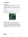
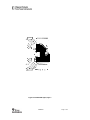
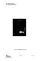
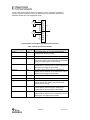
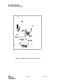
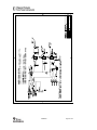
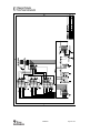
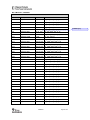
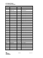
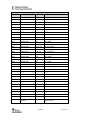
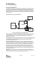
User Manual
Rev. 1.1
CC2400DK Development Kit
SWRU050
Page 1 of 35
Table of contents
INTRODUCTION ....................................................................................................................... 3
EVALUATION MODULE........................................................................................................... 4
CIRCUIT DESCRIPTION .............................................................................................................. 4
PCB LAYOUT ........................................................................................................................... 4
SCHEMATIC ............................................................................................................................ 10
EVALUATION BOARD ........................................................................................................... 12
POWER SUPPLY SECTION ........................................................................................................ 12
USB INTERFACE ..................................................................................................................... 14
RS-232 INTERFACE ................................................................................................................ 14
JUMPERS ............................................................................................................................... 14
MICROCONTROLLER AND FPGA.............................................................................................. 15
CONNECTORS ........................................................................................................................ 16
PCB LAYOUT ......................................................................................................................... 17
SCHEMATICS, CC2400EB...................................................................................................... 20
BILL OF MATERIALS, CC2400EB ............................................................................................ 25
USING THE DEVELOPMENT KIT.......................................................................................... 31
CC2400 RF EVALUATION USING SMARTRF® STUDIO............................................................... 31
USING THE CC2400DK FOR PROTOTYPING ............................................................................. 32
TROUBLESHOOTING ............................................................................................................ 33
IT DOES NOT WORK ................................................................................................................. 33
SMARTRF® STUDIO DOES NOT RECOGNIZE THE CC2400EB .................................................... 33
SWRU050
Page 2 of 35
Introduction
The CC2400 single-chip RF transceiver provides a highly integrated, flexible low-cost solution
for applications using the worldwide unlicensed 2.4 GHz frequency band. The CC2400DK
development kit is a powerful and flexible tool specifically designed to make it easy for the
user to evaluate the RF performance of the CC2400 and to minimize the time spent on
evaluation.
The Development Kit includes two Evaluation Boards and two Evaluation Modules. The
Evaluation Modules contain the CC2400 chip and required external components.
The Evaluation Board serves as a motherboard for the Evaluation Modules. The Evaluation
Board provides a USB port, a serial port, buttons, LEDs, voltage regulator, configuration
jumpers and connectors to make it easy to interface the CC2400 with the SmartRF® Studio
software and various test equipment.
This User Manual describes how to use the Development Kit. SmartRF® Studio is
documented in its own user manual.
Your SmartRF® CC2400DK Development Kit should contain the following items:
Kit contents
Item
Number of articles
Evaluation Board (CC2400EB)
2
Evaluation Module (CC2400EM)
2
Quick Start instructions
1
Antenna, 50Ω quarter-wave monopole, SMA male connector
2
SMA to BNC adapters
4
USB cable
2
CC2400 sample kit
1
SWRU050
Page 3 of 35
Evaluation Module
The Evaluation Module contains the CC2400 chip together with the needed external circuitry
for operation. Not all components are needed in an actual application. Please see the
datasheet for a typical application circuit.
The CC2400 operates in the 2.4 GHz frequency band. Although this frequency band is
usually described as “world-wide”, some countries do not allow unlicensed operation in this
band. Please refer to application note AN001 for more information about applicable
regulations.
Important: Contact your local telecommunication authorities before transmitting an RF signal.
Circuit description
The CC2400 RF section includes all the necessary components for correct operation.
The CC2400 is connected to a 16 MHz crystal.
The Evaluation Module can be plugged into the Evaluation Board. Two 2x10 pin pin row
connectors with 0.050-inch pitch are used for this purpose.
Figure 1: CC2400EM Evaluation Module
PCB layout
RF circuits operating at high frequencies are sensitive to the physical layout of the PCB.
Chipcon has carefully optimized the layout of the CC2400EM evaluation module and we
therefore recommend that the user copies it when making own PCB designs.
The PCB is of a 4-layer type in order to provide a well-defined ground plane as well as
adequate routing space. The laminate used is standard FR-4 board material. The PCB is
1.0mm thick, with layer 1 on the top side, layers 2 and 3 are internal layers and layer 4 is on
the bottom side. Layers 1 and 4 are used for routing, while layer 2 is a ground plane and layer
3 is used for power routing. All areas not utilized for routing are filled with copper connected
to ground to provide RF shielding. The ground planes on all layers are stitched together with
closely spaced vias.
SWRU050
Page 4 of 35
Figure 2: CC2400EM PCB layout, layer 1
SWRU050
Page 5 of 35
Figure 3: CC2400EM PCB layout, layer 2
SWRU050
Page 6 of 35
Figure 4: CC2400 PCB layout, layer 3
SWRU050
Page 7 of 35
Figure 5: CC2400EM PCB layout, layer 4
SWRU050
Page 8 of 35
Figure 6: CC2400EM component placement, top side (left) and bottom side (right)
SWRU050
Page 9 of 35
Schematic
SWRU050
Page 10 of 35
Bill of materials, CC2400EM
Bill of materials, CC2400EM
Reference
Description
Value
Part
C1
Capacitor 0603
2.2 µF, 10%
C_2U2_0603_X5R_K_10
C11
Capacitor 0402
100 nF, 10%
C_100N_0402_X5R_J_10
C61
Capacitor 0402
0.5 pF, ± 0.25 pF
C_0P5_0402_NP0_C_50
C62
Capacitor 0402
5.6 pF, ± 0.25 pF
C_5P6_0402_NP0_C_50
C71
Capacitor 0402
100 nF, 10%
C_100N_0402_X5R_J_10
C81
Capacitor 0402
0.5 pF, ± 0.25 pF
C_0P5_0402_NP0_C_50
C101
Capacitor 0402
10 nF, 10%
C_10N_0402_X7R_K_25
C161
Capacitor 0402
68 pF, 5%
C_68P_0402_NP0_J_50
C251
Capacitor 0402
100 nF, 10%
C_100N_0402_X5R_K_10
C261
Capacitor 0402
100 nF, 10%
C_100N_0402_X5R_K_10
C411
Capacitor 0402
68 pF, 5%
C_68P_0402_NP0_J_50
C421
Capacitor 0402
27 pF, 5%
C_27P_0402_NP0_J_50
C431
Capacitor 0402
27 pF, 5%
C_27P_0402_NP0_J_50
C481
Capacitor 0402
68 pF, 5%
C_68P_0402_NP0_J_50
L61
Inductor 0402
7.5 nH, 5%
L_7N5_0402_J
L62
Inductor 0402
5.6 nH, 5%
L_5N6_0402_J
L71
Inductor 0402
27 nH, 5%
L_27N_0402_J
L81
Inductor 0402
7.5 nH, 5%
L_7N5_0402_J
P1
SMD pinrow socket
SMD_SOCKET_2x10 (Samtec
SFM-110-02-S-D-A-K-TR)
P2
SMD pinrow socket
SMD_SOCKET_2x10 (Samtec
SFM-110-02-S-D-A-K-TR)
P4
Surface-mount
SMA, straight
SMA_SMD
R1
Resistor 0402
2.2 Ω, 5%
R2R2_0402_J
R451
Resistor 0402
43 kΩ, 1%
R_43K_0402_F
U1
Single-chip
transceiver
CC2400
X1
Crystal, ceramic
SMD 4x25mm
X_16.000/10/10/10/16 (Toyocom
TSX-10A 16M 16pF)
Note: The crystal X1 mounted on the EM board is a 16.000 MHz crystal, with ±10 ppm initial
tolerance, ± 10 ppm drift over temperature and a temperature range of -10˚ C to +60˚ C. The
crystal is designed for 16 pF load capacitance. In an actual application, the tolerance, drift
and temperature range of the crystal must be considered with application requirements in
mind. Please consult the data sheet and SmartRF® Studio for more information. It is possible
to choose a larger crystal package to save cost. The crystal should have an ESR of 60 Ω or
less.
SWRU050
Page 11 of 35
Evaluation Board
The Evaluation Board is used as a motherboard for the Evaluation Modules and provides
power and external connections.
Power
connections
Jumpers
Sockets for EM
Buttons
DC jack
LEDs
SMA connectors
Serial port
USB port
Test port
Reset button
Figure 7: CC2400EB Evaluation Board
Power supply section
The power supply section is configured by moving the jumpers located on the board. There
are three voltage regulators on the board, one for use by the FPGA, a 3.3 V regulator for
general use and a 1.8 V regulator for powering the CC2400. The voltage regulator for the
FPGA is turned on under software control when the USB controller has been properly
configured.
A diode prevents permanent damage if wrong polarity is applied to the non-regulated input.
There are two power connectors; a 3.5mm DC jack-type connector allows you to connect an
unregulated battery eliminator easily (the positive supply is on the center pin), and two 5-pin
terminal blocks can be used to connect either an unregulated or regulated power supply.
An amperemeter can also be connected in order to measure the DC current drawn by the
CC2400. Since the CC2400 has two voltage supplies (Core and I/O), there are separate
SWRU050
Page 12 of 35
current measurement loops for these two supplies. If you are not going to measure the
currents, short-circuit jumpers must be connected between the terminals, otherwise the
Evaluation Module will not be supplied with power.
A
IOC
IIC
ExtC
0V
P2
0V
IOI
A
III
ExtI
0V
P3
4-7V
Figure 8: Power terminal block with amperemeters attached
Table 1: Power connector connections
Connector and pin
Marking
Description
P3 pin 1
4-7V
Unregulated voltage in. Input to voltage regulators.
Equivalent with the DC jack input.
P3 pin 2
0V
Circuit ground.
P3 pin 3
ExtI
External I/O voltage. An externally applied voltage will
drive the I/O supply of the CC2400 (and the associated
FPGA pins) if the jumpers are set correctly.
P3 pin 4
III
I/O supply current input. Insert an amperemeter
between this pin and the IOI pin to measure the current
drawn by the I/O supply of the CC2400.
P3 pin 5
IOI
I/O supply current output. Insert an amperemeter
between this pin and the III pin to measure the current
drawn by the I/O supply of the CC2400.
P2 pin 1
0V
Circuit ground.
P2 pin 2
0V
Circuit ground.
P2 pin 3
Ext C
External core voltage. An externally applied voltage
that will drive the core supply of the CC2400 if the
jumpers are set correctly.
P2 pin 4
IIC
Core voltage current input. Insert an amperemeter
between this pin and the IOC pin to measure the
current drawn by the core supply of the CC2400.
P2 pin 5
IOC
Core voltage current output. Insert an amperemeter
between this pin and the IIC pin to measure the current
drawn by the core supply of the CC2400.
SWRU050
Page 13 of 35
USB interface
The CC2400EB connects to a PC via a USB interface. SmartRF® Studio uses the USB
interface to control the CC2400EB. The USB interface can be used both to configure the
CC2400 and transfer data. Chipcon provides a Windows driver that is installed as part of the
SmartRF® Studio installation process. This driver must be present for SmartRF® Studio to
communicate with the CC2400EB.
Because USB is used, the CC2400DK will only function with PCs running Windows 98,
Windows ME, Windows 2000, Windows XP or newer. Windows NT and Windows 95 cannot
be used since they do not support USB.
RS-232 interface
A serial port is included on the CC2400EB. This is intended for debugging purposes, and
cannot be used to connect the Evaluation Board to SmartRF® Studio.
Jumpers
The jumpers are used to configure the Evaluation Board. The factory default settings are
shown below, please return to these settings if you are experiencing any problems.
Figure 9 Default jumper settings
SWRU050
Page 14 of 35
Jumpers
Name
Default setting
Description
VIO
Between pins
6 and 8
Determines how the I/O supply of the CC2400 is supplied
with power. If the jumper is connected between pins 8 and
6, the 1.8V supply is used. If the jumper is connected
between pins 8 and 10, the 3.3V supply is used. If the
jumper is connected between pins 8 and 7, the I/O supply is
driven by the external voltage present on the ExtI pin on the
power connector.
VC
Between pins
3 and 5
Determines how the core supply of the CC2400 is supplied
with power. If the jumper is connected between pins 3 and
5, power is supplied by the 1.8V regulator. If the jumper is
connected between pins 3 and 1, the core supply is driven
by the external voltage present on the ExtC pin on the
power connector.
V
Between pins
4 and 6
Determines how power is supplied to the board. If the
jumper is connected between pins 4 and 6, the EB is
powered from the power connected to the power connector
or the power jack. If the jumper is connected between pins
6 and 8, the EB is powered from the USB bus. In this case,
the USB port the EB is connected to must be able to supply
500 mA current.
EEPROM
En.
Present
Determines if USB configuration information is loaded from
EEPROM memory. If removed, the CC2400EB will report
itself as a default USB device. This jumper should always
be present during normal operation.
Microcontroller and FPGA
The CC2400EB has been built around a Cypress USB microcontroller and a Xilinx Spartan II
200E FPGA. This has been done to ensure maximum flexibility and is not representative for a
low-cost CC2400 application.
Both the microcontroller and the FPGA are RAM-based devices, and their configuration is
loaded via the USB interface on power-up. The CC2400EB must therefore be connected to a
PC to function properly.
Four LEDs and two buttons are included on the board for user interface purposes. The LEDs
are driven by the FPGA, while the buttons are connected to both the FPGA and the
microcontroller.
A reset button is provided, which will reset both the microcontroller and the USB interface.
The LEDs are used to indicate status when the CC2400EB is used together with SmartRF®
Studio.
SWRU050
Page 15 of 35
Connectors
The Evaluation Board is furnished with many connectors for easy access to various signals.
Test Port 1 (P17) and Test Port 2 (P5) are 2x10 pin pin-row connectors that are connected to
the FPGA and can be used to monitor various signals, including all the CC2400 signals. The
pin-out of these connectors is compatible with logic analyzer probes from Agilent.
The DTEST1 (P6) and DTEST2 (P7) SMA connectors are also connected to the FPGA and
can be used to output or input signals from/to the CC2400, respectively.
The ATEST1 (P9) and ATEST2 (P8) provide access to analog test signals from the CC2400.
The selection of what signals are available at the different connectors is done in SmartRF®
Studio.
SWRU050
Page 16 of 35
PCB layout
The Evaluation Board is a 4-layer, 1.6 mm thick FR-4 PCB. Four layers are used because of
the routing requirements. Layers 1 and 4 are used for signal routing, layer 2 is a ground plane
and layer 3 is used for power routing. The majority of the components are mounted on the top
side of the PCB, while a few decoupling capacitors were put on the bottom side.
Figure 10: CC2400EB PCB layout, layer 1 (top left), layer 2 (top right), layer 3 (bottom left)
and layer 4 (bottom right)
SWRU050
Page 17 of 35
Figure 11: CC2400EB component placement, top side
SWRU050
Page 18 of 35
Figure 12: CC2400EB component placement, bottom side
SWRU050
Page 19 of 35
Schematics, CC2400EB
SWRU050
Page 20 of 35
SWRU050
Page 21 of 35
SWRU050
Page 22 of 35
SWRU050
Page 23 of 35
SWRU050
Page 24 of 35
Bill of Materials, CC2400EB
Bill of materials, CC2400EB Evaluation Board
Reference
Description
Value
Part
C1
Capacitor 1206
2.2 µF, 10%
C_2U2_1206_X7R_K_10
C2
Capacitor 0603
27 pF, 5%
C_27P_0603_NP0_J_50
C3
Capacitor 0603
27 pF, 5%
C_27P_0603_NP0_J_50
C4
Capacitor, tantal
3.3 µF
C_3U3_TAN_B
C5
Capacitor 1206
2.2 µF, 10%
C_2U2_1206_X7R_K_10
C6
Capacitor 0603
33 nF, 10%
C_33N_0603_X7R_K_25
C14
Capacitor 0603
100 nF, 10%
C_100N_0603_X7R_K_50
C15
Capacitor, tantal
3.3 uF
C_3U3_TAN_B
C16
Capacitor 0603
100 nF, 10%
C_100N_0603_X7R_K_50
C17
Capacitor 0603
100 nF, 10%
C_100N_0603_X7R_K_50
C18
Capacitor 0603
100 nF, 10%
C_100N_0603_X7R_K_50
C19
Capacitor 0603
100 nF, 10%
C_100N_0603_X7R_K_50
C20
Capacitor 0603
100 nF, 10%
C_100N_0603_X7R_K_50
C21
Capacitor 0603
100 nF, 10%
C_100N_0603_X7R_K_50
C22
Capacitor 0603
100 nF, 10%
C_100N_0603_X7R_K_50
C23
Capacitor 0603
100 nF, 10%
C_100N_0603_X7R_K_50
C24
Capacitor 0603
100 nF, 10%
C_100N_0603_X7R_K_50
C25
Capacitor 0603
100 nF, 10%
C_100N_0603_X7R_K_50
C26
Capacitor 0603
33 nF, 10%
C_33N_0603_X7R_K_25
C27
Capacitor 0603
33 nF, 10%
C_33N_0603_X7R_K_25
C28
Capacitor 0603
33 nF, 10%
C_33N_0603_X7R_K_25
C29
Capacitor 0603
33 nF, 10%
C_33N_0603_X7R_K_25
C30
Capacitor 0603
33 nF, 10%
C_33N_0603_X7R_K_25
C31
Capacitor 0603
33 nF, 10%
C_33N_0603_X7R_K_25
C32
Capacitor 0603
33 nF, 10%
C_33N_0603_X7R_K_25
C33
Capacitor 0603
33 nF, 10%
C_33N_0603_X7R_K_25
C34
Capacitor 0603
33 nF, 10%
C_33N_0603_X7R_K_25
C35
Capacitor 0603
33 nF, 10%
C_33N_0603_X7R_K_25
C36
Capacitor 0603
33 nF, 10%
C_33N_0603_X7R_K_25
C37
Capacitor 0603
33 nF, 10%
C_33N_0603_X7R_K_25
C38
Capacitor, tantal
47 µF
C_47U_TAN_D
C39
Capacitor 0603
33 nF, 10%
C_33N_0603_X7R_K_25
C40
Capacitor 0603
33 nF, 10%
C_33N_0603_X7R_K_25
C41
Capacitor 0603
33 nF, 10%
C_33N_0603_X7R_K_25
SWRU050
Comment [C1]:
Page 25 of 35
Bill of materials, CC2400EB Evaluation Board
Reference
Description
Value
Part
C42
Capacitor 0603
33 nF, 10%
C_33N_0603_X7R_K_25
C43
Capacitor 0603
33 nF, 10%
C_33N_0603_X7R_K_25
C44
Capacitor 0603
33 nF, 10%
C_33N_0603_X7R_K_25
C45
Capacitor 0603
33 nF, 10%
C_33N_0603_X7R_K_25
C46
Capacitor 0603
33 nF, 10%
C_33N_0603_X7R_K_25
C47
Capacitor 0603
33 nF, 10%
C_33N_0603_X7R_K_25
C48
Capacitor, tantal
47 µF
C_47U_TAN_D
C49
Capacitor, tantal
47 µF
C_47U_TAN_D
C50
Capacitor 0603
33 nF, 10%
C_33N_0603_X7R_K_25
C51
Capacitor 0603
33 nF, 10%
C_33N_0603_X7R_K_25
C52
Capacitor 0603
33 nF, 10%
C_33N_0603_X7R_K_25
C53
Capacitor, tantal
47 µF
C_47U_TAN_D
C54
Capacitor 0603
33 nF, 10%
C_33N_0603_X7R_K_25
C55
Capacitor 0603
33 nF, 10%
C_33N_0603_X7R_K_25
C56
Capacitor 0603
33 nF, 10%
C_33N_0603_X7R_K_25
C57
Capacitor, tantal
47 µF
C_47U_TAN_D
C58
Capacitor 0603
33 nF, 10%
C_33N_0603_X7R_K_25
C59
Capacitor 0603
33 nF, 10%
C_33N_0603_X7R_K_25
C60
Capacitor 0603
33 nF, 10%
C_33N_0603_X7R_K_25
C61
Capacitor, tantal
47 µF
C_47U_TAN_D
C62
Capacitor 0603
33 nF, 10%
C_33N_0603_X7R_K_25
C63
Capacitor 0603
33 nF, 10%
C_33N_0603_X7R_K_25
C64
Capacitor 0603
33 nF, 10%
C_33N_0603_X7R_K_25
C65
Capacitor, tantal
47 µF
C_47U_TAN_D
C66
Capacitor, tantal, low
ESR
100 µF
C_100U_TAN_D_KEMET (Kemet
T494D107M010AS)
C67
Capacitor, tantal
47 µF
C_47U_TAN_D
C68
Capacitor 0603
33 nF, 10%
C_33N_0603_X7R_K_25
C69
Capacitor 0603
33 nF, 10%
C_33N_0603_X7R_K_25
C70
Capacitor 0603
33 nF, 10%
C_33N_0603_X7R_K_25
C71
Capacitor 0603
33 nF, 10%
C_33N_0603_X7R_K_25
C100
Capacitor 0603
100 nF, 10%
C_100N_0603_X7R_K_50
C101
Capacitor 0603
100 nF, 10%
C_100N_0603_X7R_K_50
C102
Capacitor 0603
100 nF, 10%
C_100N_0603_X7R_K_50
C103
Capacitor low
impedance
470 µF,
electrolytic
C_470U_8_CVAX (Sanyo CV-AX
8x10,2)
SWRU050
Page 26 of 35
Bill of materials, CC2400EB Evaluation Board
Reference
Description
Value
Part
C104
Capacitor 0603
100 nF, 10%
C_100N_0603_X7R_K_50
C105
Capacitor 0603
33 nF, 10%
C_33N_0603_X7R_K_25
C106
Capacitor 1206
2.2 µF, 10%
C_2U2_1206_X7R_K_10
D1
Schottky diode, 2A
20BQ030, International Rectifier
D2
LED, green, SMD
LED_CL150GCD, Citizen
D3
LED, red, SMD
LED_CL150URCD, Citizen
D4
LED, yellow, SMD
LED_CL150YCD, Citizen
D5
LED, blue, SMD
LED_EL15-21UBC, Everlight
H1
Circuit board support
Distance 12.5mm
H2
Circuit board support
Distance 12.5mm
H3
Circuit board support
Distance 12.5mm
H4
Circuit board support
Distance 12.5mm
P1
D-SUB, 9 pin, female
DSUB_9F
P2
5-pin terminal, screw
SCREW_TERM_5
P3
5-pin terminal, screw
SCREW_TERM_5
P4
DC jack, 2.5mm center
pin
DC_JACK_2.5
P5
Pin row connector,
2x10
PINROW_2_10
P6
SMA connector
SMA (Right angle)
P7
SMA connector
SMA (Right angle)
P8
SMA connector
SMA (Right angle)
P9
SMA connector
SMA (Right angle)
P10
Pin row connector, 2x5
PINROW_2X5
P11
Pin row connector, 2x5
PINROW_2X5
P12
Pin row connector, 2x5
PINROW_2X5
P13
SMD pinrow header
SMD_HEADER_2x10 (Samtec TFM110-02-S-D-A-K-TR)
P14
SMD pinrow header
SMD_HEADER_2x10 (Samtec TFM110-02-S-D-A-K-TR)
P15
USB B-type connector
USB_B (AMP 787780-1)
P16
Low-profile pin row
connector, 1x6
CON6_FEMALE_LP (Preci-DIP 80191-006-10-012)
P17
Pin row connector,
2x10
PINROW_2X10
P18
Low-profile pin row
connector, 1x6
CON6_FEMALE_LP (Preci-DIP 80191-006-10-012)
SWRU050
Comment [C2]:
Page 27 of 35
Bill of materials, CC2400EB Evaluation Board
Reference
Description
Value
Part
P19
Do not mount
DNM
P20
Low-profile pin row
connector, 1x6
CON6_FEMALE_LP (Preci-DIP 80191-006-10-012)
Q1
PNP, general-purpose
BC857B (Philips)
Q2
NPN, small-signal
BC846B (Philips)
R1
Resistor 0603
10 kΩ, 2%
R_10K_0603_G
R2
Resistor 0603
22 Ω, 2%
R_22_0603_G
R3
Resistor 0603
22 Ω, 2%
R_22_0603_G
R4
Resistor 0603
1.5 kΩ, 2%
R_1K5_0603_G
R5
Resistor 0603
1 MΩ, 5%
R_1M0_0603_J
R6
Resistor 0603
47 kΩ, 2%
R_47K_0603_G
R7
Resistor 0603
47kΩ, 2%
R_47K_0603_G
R8
Resistor 0603
0Ω
R_0_0603
R9
Resistor 0603
0Ω
R_0_0603
R10
Do Not Mount
DNM
R11
Do Not Mount
DNM
R12
Resistor 0603
47kΩ, 2%
R_47K_0603_G
R13
Resistor 0603
47kΩ, 2%
R_47K_0603_G
R14
Resistor 0603
0Ω
R_0_0603
R15
Resistor 0603
47 kΩ, 2%
R_47K_0603_G
R16
Resistor 0603
47 kΩ, 2%
R_47K_0603_G
R17
Do Not Mount
R18
Resistor 0603
R19
Do Not Mount
R20
Resistor 0603
R21
Do Not Mount
R22
Resistor 0603
1 kΩ, 5%
R_1K0_0605_J
R23
Resistor 0805
270 Ω, 5%
R_270_0805_J
R24
Resistor 0805
330 Ω, 5%
R_330_0805_J
R25
Resistor 0805
270 Ω, 5%
R_270_0805_J
R26
Resistor 0805
270 Ω, 5%
R_270_0805_J
R27
Resistor 0603
1 kΩ, 5%
R_1K0_0605_J
R28
Resistor 0603
1 kΩ, 5%
R_1K0_0605_J
R29
Resistor 0603
0Ω
R_0_0603
R30
Do Not Mount
DNM
47kΩ, 2%
R_47K_0603_G
DNM
47 kΩ, 2%
R_47K_0603_G
DNM
DNM
SWRU050
Page 28 of 35
Bill of materials, CC2400EB Evaluation Board
Reference
Description
Value
Part
R31
Resistor 0603
0Ω
R_0_0603
R32
Do Not Mount
R33
Resistor 0603
R34
Do Not Mount
DNM
R35
Do Not Mount
DNM
R36
Do Not Mount
DNM
R37
Do Not Mount
DNM
R38
Do Not Mount
DNM
R39
Do Not Mount
DNM
R40
Resistor 0603
47 kΩ, 2%
R_47K_0603_G
R41
Resistor 0603
0Ω
R_0_0603
R42
Resistor 0603
47 kΩ, 2%
R_47K_0603_G
R43
Resistor 0603
47 kΩ, 2%
R_47K_0603_G
R44
Resistor 0603
47 kΩ, 2%
R_47K_0603_G
R45
Resistor 0603
1 kΩ, 5%
R_1K0_0605_J
R46
Resistor 0603
10 kΩ, 2%
R_10K_0603_G
R47
Resistor 0603
0Ω
R_0_0603
R100
Resistor 0603
0Ω
R_0_0603
R101
Resistor 0603
0Ω
R_0_0603
S1
Push button, SMD
SKHUAF, Alps
S2
Push button, SMD
SKHUAF, Alps
S3
Push button, SMD
SKHUAF, Alps
TP1
Test point
TESTPIN
TP2
Test point
TESTPIN
TP3
Test point
TESTPIN
TP4
Test point
TESTPIN
TP5
Test point
TESTPIN
TP6
Test point
TESTPIN
TP7
Test point
TESTPIN
TP8
Test point
TESTPIN
U1
EZ-USB MCU
CY7C64613-128NC, Cypress
U2
Spartan IIE FPGA
XC2S200E-6FT256I, Xilinx
U3
Do Not Mount
DNM
U4
3.3 V low drop-out
regulator
LP2981AIM5-3.3, National
Semiconductor
DNM
47 kΩ, 2%
SWRU050
R_47K_0603_G
Page 29 of 35
Bill of materials, CC2400EB Evaluation Board
Reference
Description
Value
U5
32 kB SRAM
IDT71V256SA20YI, IDT
U6
1.8 V low drop-out
regulator
XC6204B182MR, Torex
U7
1.8 V low drop-out
regulator, 800 mA
LP3961ES-1.8, National
Semiconductor
U8
16 byte I2C EEPROM
24LC00I/SN, Microchip
U9
Do Not Mount
DNM
U10
Do Not Mount
DNM
U11
Quad NAND gate
74HC00D, Philips
U100
RS-232 Transceiver,
3-5V
MAX3243EEWI, Maxim
X1
12 MHz crystal, HC49SMD, 50/50 ppm,
12 pF
X_12.000/50/50/10/12
SWRU050
Part
Page 30 of 35
Using the Development Kit
The Development Kit is useful for providing hands-on experience with the CC2400 for both
software and hardware developers. The plug-in Evaluation Module provides flexibility; it can
operate both in a stand-alone fashion and together with the Evaluation Board. Using the
Evaluation Board, it is easy to interface the CC2400 with both test equipment and additional
application circuitry without having to make a PCB from scratch. Below we will highlight the
most useful setups.
CC2400 RF Evaluation using SmartRF® Studio
Spectrum
analyzer / RF
Signal generator
CC2400
EM
PC running
SmartRF Studio
CC2400
Evaulation Board
Oscilloscope /
Function
generator
Figure 13: RF Evaluation using SmartRF® Studio
Using the setup shown in Figure 13, the RF performance of the CC2400 can be evaluated.
Use the supplied cable to connect the USB port of the CC2400EB to the USB port of a PC
running SmartRF® Studio. You can then use SmartRF® Studio to control all the RF
parameters of the CC2400.
SmartRF® Studio can be used to perform a wide variety of RF tests, including link tests. Using
two CC2400EBs, it is possible to send data from one PC to another. It is also possible to test
a frequency-hopping link in the same fashion. Please refer to the SmartRF® Studio
documentation for more information.
When the CC2400EB board is connected to a PC, the PC will load the USB driver for the
board (SmartRF® Studio must be installed on the PC). Once the driver has loaded, it will
update the FPGA and microcontroller, and the LEDs will start flashing. The LED flashing will
stop if one of the buttons on the board is pressed, or when SmartRF® Studio is started.
When SmartRF Studio is running, the LEDs are used to indicate the FH network ID for the
board. The ID is shown as a binary number, with the red LED representing the least
significant bit (LSB), the yellow LED representing bit 1, and the green LED representing the
most significant bit (MSB). When FH network is active, the blue LED toggles each time the
status is read from the PC.
Important: The use of radio transceivers is regulated by international and national rules.
Before transmitting an RF signal on an antenna, please contact your local telecommunication
authorities to make sure that you are licensed to operate the transceiver.
SWRU050
Page 31 of 35
Using the CC2400DK for prototyping
The CC2400EM module contains the CC2400 and all external components required. All
CC2400 signals are available at the SMD connectors on the bottom side of the module. The
modules can be easily plugged into a prototype PCB containing the rest of the system. The
SMD connectors used on the CC2400EM are manufactured by Samtec
(http://www.samtec.com/), please refer to the CC2400EB bill of materials for the part number
of the connector that will interface with the connectors on the EM.
It is also possible to do prototyping by connecting any microcontroller development kit to the
CC2400EB through Test Port 1. The FPGA must then be programmed using the SmartRF
Studio “Load FPGA Configuration” function at startup. The
“fpga_cc2400_uc_prototyping_1_0.bin” FPGA file is downloadable from the Chipcon website.
All LEDs will be turned off after programming this FPGA. The FPGA will give access to all
CC2400 digital pins on Test Port 1, as shown below.
Test Port 1 Pin Number
Test Port 1 (to / from uC)
1
N/C
2
N/C
3
N/C
4
DIO/PKT (to uC)
5
HighZ
6
HighZ
7
HighZ
8
DCLK/FIFO (to uC)
9
HighZ
10
HighZ
11
HighZ
12
CSn (from uC)
13
SCLK (from uC)
14
SI (from uC)
15
SO (to uC)
16
GIO1 (to uC)
17
GIO6 (to uC)
18
TX (from uC)
19
RX (from uC)
20
GND
Test Port 2 contains the same pins, except these are all outputs from the FPGA. Test Port 2
may be connected to a Logic Analyzer for software debugging purposes.
It should be noted that when using a ribbon cable from Test Port 1 to the MCU, one can
experience that some of the signals are interfering with each other.
A solution would be to use single wires instead, or use some form of shielded ribbon cable.
SWRU050
Page 32 of 35
Troubleshooting
It does not work
•
Make sure that either a jumper or an amperemeter is connected between the IOI and
II terminals and the IIC and IOC terminals on the power connector.
•
Make sure that the power supply is connected to the correct pins on the power
connector.
•
Is the supply voltage correctly polarized? If not, the protection diode will prevent any
current from flowing. + and – are indicated on the PCB. On the DC jack, the tip is +
and the ring is –.
•
Please note that the CC2400EB must be connected to a PC for proper operation. The
FPGA and microcontroller are RAM-based, and firmware must be loaded from a PC
when power is applied to the board.
•
If the USB driver is loaded correctly, you should see the LEDs on the CC2400EB
flash. The LEDs will stop flashing when one of the buttons on the CC2400EB is
pressed or when SmartRF® Studio is started.
SmartRF® Studio does not recognize the CC2400EB
•
Make sure that you have installed SmartRF® Studio using the installation program.
•
Make sure that the USB port on your computer is installed correctly (try another USB
device with the same port). Also note that USB only works correctly with Windows 98,
ME, 2000, XP or newer.
•
Please note that SmartRF® Studio can only communicate with the CC2400EB via the
USB port. The serial port cannot be used to communicate with the CC2400EB.
Document History
Revision
Date
Description/Changes
1.0
2003-10-01
Initial release.
1.1
2004-04-19
Added information about FPGA configuration for prototyping with an
external microcontroller.
Minor corrections.
C421 and C431 changed to 27 pF.
SWRU050
Page 33 of 35
Disclaimer
Chipcon AS believes the information contained herein is correct and accurate at the time of this printing. However,
Chipcon AS reserves the right to make changes to this product without notice. Chipcon AS does not assume any
responsibility for the use of the described product.; neither does it convey any license under its patent rights, or the
rights of others. The latest updates are available at the Chipcon website or by contacting Chipcon directly.
As far as possible, major changes of product specifications and functionality will be stated in product specific Errata
Notes published at the Chipcon website. Customers are encouraged to sign up for the Developer’s Newsletter in
order to receive the most recent updates on products and support tools.
When a product is discontinued this will be done according to Chipcon’s procedure for obsolete products as
described in Chipcon’s Quality Manual. This includes informing about last-time-buy options. The Quality Manual can
be downloaded from Chipcon’s website.
Trademarks
SmartRF® is a registered trademark of Chipcon AS. SmartRF® is Chipcon's RF technology platform with RF library
cells, modules and design expertise. Based on SmartRF® technology Chipcon develops standard component RF
circuits as well as full custom ASICs based on customer requirements and this technology.
All other trademarks, registered trademarks and product names are the sole property of their respective owners.
© 2003, Chipcon AS. All rights reserved.
SWRU050
Page 34 of 35
Address Information
Web site:
http://www.chipcon.com
E-mail:
[email protected]
Technical Support Email:
[email protected]
Technical Support Hotline:
+47 22 95 85 45
Headquarters:
Chipcon AS
Gaustadalléen 21
NO-0349 Oslo
NORWAY
Tel: +47 22 95 85 44
Fax: +47 22 95 85 46
E-mail: [email protected]
US Offices:
Chipcon Inc., Western US Sales Office
19925 Stevens Creek Blvd.
Cupertino, CA 95014-2358
USA
Tel: +1 408 973 7845
Fax: +1 408 973 7257
Email: [email protected]
Chipcon Inc., Eastern US Sales Office
35 Pinehurst Avenue
Nashua, New Hampshire, 03062
USA
Tel: +1 603 888 1326
Fax: +1 603 888 4239
Email: [email protected]
Sales Office Germany:
Chipcon AS
Riedberghof 3
D-74379 Ingersheim
GERMANY
Tel: +49 7142 9156815
Fax: +49 7142 9156818
Email: [email protected]
Strategic Automotive Center:
Chipcon AS
Hechtseestrasse 16
D-83022 Rosenheim
GERMANY
Tel: +49 8031 2227 660
Fax: +49 8031 2227 661
Email: [email protected]
Sales Office Asia :
Chipcon Asia Pacific
37F, Asem Tower
159-1 Samsung-dong, Kangnam-ku
Seoul 135-798 Korea
Tel: +82 2 6001 3888
Fax: +82 2 6001 3711
Email: [email protected]
SWRU050
Page 35 of 35