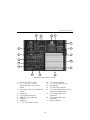
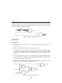
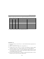
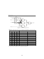
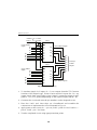
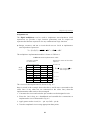
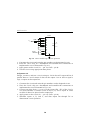
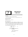
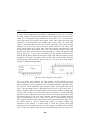
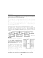
1
DIGITAL LOGIC DESIGN
DIGITAL
LOGIC DESIGN
Press No: 42
Second Edition
Qafqaz University Press
Bakı - 2010
Ministry of Education of
Azerbaijan Republic
“Çağ” Educational
Corporation
Institute of Educational
Problems
Qafqaz University
DIGITAL LOGIC DESIGN
LABORATORY MANUAL
Second Edition
Khalil Ismailov
Approved by the decision of the ScientificMethodical Commission’s “Informatics and
Computer Technologies” Section of the
Ministry of Education of Azerbaijan Republic
dated January 16, 2007 (minute No. 01)
Baku, 2010
DIGITAL LOGIC DESIGN
LABORATORY MANUAL
Second Edition
Prepared by
Kh. A. Ismailov, Professor
Department of Computer Engineering,
Qafqaz University
Reviewed by
T.A. Alizade, PhD
The Institute of Cybernetics of the National
Academy of Sciences of Azerbaijan Republic
S.B. Habibullaev, Associate Professor
Department of Computer Technologies and Programming,
Azerbaijan State Oil Academy
Editor
A.Z. Melikov, Professor
Associate Member of the National
Academy of Sciences of Azerbaijan Republic,
The Institute of Cybernetics of the National
Academy of Sciences of Azerbaijan Republic
Design
Sahib Kazimov
Is published as a Qafqaz University publication by the
proposal of the Publishing Committee dated from 04.10.2006
(minute No. Ç-QU-250-300/020) and decision of the Senate
dated from 11.10.2006 (minute No. Ç-QU-105-400/23)
Book is printed by “Sharg-Qarb” Publishing House.
© Qafqaz University 2010
Press No: 42
CONTENTS
Preface
1
Experiment Guidelines
2
Generating Digital Signals for Testing
2
Detecting Logic Signals
5
Logic Probes
7
Logic Pulsers
7
Power Supplies
7
Digital Logic Trainer Y-0039
8
Experiment 1. Digital Logic Circuits
11
Experiment 2. Simplification of Boolean Functions
19
Experiment 3. Basic Design of Combinational Circuits
27
Experiment 4. Karnaugh Maps and Design Minimization
33
Experiment 5. Code Converters
40
Experiment 6. Design with Multiplexers and Demultiplexers
48
Experiment 7. Arithmetic Circuits
63
Experiment 8. Properties of Latches/Flip-Flops
71
Experiment 9. Ripple Counter Design
82
Experiment 10. Synchronous Counter Analysis
91
Experiment 11. Registers
98
Experiment 12. Shift Register Counters
105
i
REFERENCES
113
APPENDIX A
114
APPENDIX B
120
APPENDIX C
130
APPENDIX D
150
APPENDIX E
165
ii
PREFACE
This manual is designed to provide practical laboratory experience for the
student of digital electronics. The manual includes experiments on digital
fundamentals and design. It is not intended that all the experiments be
completed or that every experiment be done in its intirety. Instructors will
probably want to make certain exercises optional to the student.
Each experiment begins with a set of stated objectives, text references, and
required equipment, followed by a procedure for meeting each objective.
Most experiments specify logic circuits needed to perform the experiment,
while a few require that the student design and draw the circuit(s).
This manual contains several appendixes at the end. The students is
encouraged to become familiar with the contents of the appendixes early,
even though serious reading of much of the information on troubleshooting
and digital faults can be deferred until it is needed.
Appendix A covers the types of circuit breadboards used in laboratory
experiments for temporary circuit testing.
Appendix B covers several topics which should be helpful to the student,
Included in the material are general hints on proper breadboarding, digital
troubleshooting, and information on typical digital system and IC faults.
The information about digital ICs and 74 series family cross-reference of 155
series Russian ICs are found in Appendix C.
The pin layout for digital ICs used in experiments are found in Appendix D of
this manual.
The information about seven segment displays of type HDSP is provided in
Appendix E.
1
Khalil Ismailov
EXPERIMENT GUIDELINES
Here are some guidelines to help you perform the experiments and to submit
the reports:
• Read all instructions carefully and carry them all out.
• Ask a demonstrator if you are unsure of anything.
• Record actual results (comment on them if they are unexpected!)
• Write up full and suitable conclusions for each experiment.
• If you have any doubt about the safety of any procedure, contact the
demonstrator beforehand.
• THINK about what you are doing!
Most experiments involve the use of the power supply, the oscilloscope, a
signal generator, the voltage measurement unit and your breadboard.
GENERATING DIGITAL SIGNALS FOR TESTING
The most common type of signal needed to test logic circuits is a static signal
that can be switched HIGH or LOW with a simple single throw (SPST) switch.
New students are often confused by how to do this correctly. The problems
involved, and the solution, are illustrated in Fig. 0.1.
The problem is illustrated in (a), which shows a logic circuit to be tested, a 5 V
power supply and a switch. The logic circuit will be connected to the power
supply, and the switch should be used to provide a signal input voltage, VIN, to
the circuit such that changing the switch position will change the signal input
voltage between logic HIGH and LOW. How should the switch be connected?
It cannot be connected directly across the supply since this would short the
supply when it is closed. An arrangement sometimes tried by new students is
shown in (b). In this case, when the switch is open, the input to the circuit is
an open circuit so that the input voltage is undefined, which will not produce
correct operation of the circuit to be tested.
There are two possible solutions, which are shown in Fig. 0.l (c) and (d). In
both of these the switch is in series with a resistor between the terminals of
the power supply, but the circuit shown in (c) will not usually be satisfactory
and the circuit in (d) is one that should be used. This circuit is referred to in the
Laboratories as a static logic level signal source. The reasons why the circuit
2
Digital Logic Design
in (c) will not operate correctly are due to the properties of the inputs to TTL
and other integrated circuits. In order for TTL circuits to function correctly the
LOW input level must be below 0.8 V while the HIGH input level must be
above 2.0 V. The circuit in (c) will always produce a correct HIGH level of 5.0
V when the switch is open and the logic under test draws its current directly
from the supply. However, when the switch is closed current will flow out of
the circuit input through the resistor, R, to ground (R is called a pull-down
resistor). This produces a voltage drop across R and a LOW level input
voltage, VL, which is above ground. In TTL circuitry current flow when the
input voltage is HIGH. Thus an appreciable current flowing through R when
the switch is closed can bring the input voltage above the allowable
maximum. The only way to avoid this is to make R very small, but this will
drain a large current from the power supply when the switch is closed.
Fig. 0.1. Generating a static logic level signal
The circuit shown in (d) functions much better the student still needs to
understand its limitations. In this circuit, when the switch is closed, the input to
the test circuit is connected directly to ground so that the LOW voltage is at
zero volts regardless of the magnitude of the input current. When the switch is
3
Khalil Ismailov
open, the test circuit input voltage is connected to the +5.0 V supply through
the resistor, R. Note that whatever input current, IH, is required by the circuit
under test must flow through R and will therefore produce a voltage drop
reducing the HIGH level input voltage, VH, to a value of (5 - RIH). There are two
factors to consider. First, HIGH level input currents are considerably lower than
LOW level input currents due to the nature of the circuitry used in the
integrated circuits. Second, the HIGH level input voltage can be allowed to
drop to as low as 2.0 V without violating circuit specifications. Both of these
mean that, in most applications, the resistor, R, can be made reasonably large
so that the HIGH level voltage is properly defined without drawing too much
current from the power supply when the switch is closed. The resistor, R, is
known as pull-up resistor. When designing static logic level sources its value
must be chosen to produce adequate voltage levels for the circuits to be tested.
In almost all cases, values between 1.0 kΩ and 10.0 kΩ will work well. The
student is cautioned, however, that if a single switch circuit is to be used to
provide multiple inputs to a test circuit, it may be necessary to adjust the value
of the pull-up resistor to maintain adequate HIGH level voltages. In building a
logic circuit facility the student will need multiple static signal sources. Eight
such circuits should be sufficient for most Assignments in the Laboratories.
The second type of signal generating requirement necessary for testing logic
circuits is the ability to generate a single pulse from a manual switch. This
type of circuit is referred to in the Laboratory equipment lists as a push button
manual pulser. The pulse produced by the pulser must be "clean" with sharp
edges. Also, for greatest versatility, the pulser should be able to produce both
HIGH-going as well as LOW-going pulses. A simple SPST switch circuit such
as that of Fig. 0.l (d) cannot be used because of the problems of switch
bounce. When the mechanical contacts of the switch are closed, they actually
bounce together a multiple and indeterminate number of times before coming
to rest in a closed position. This produces a voltage that switches between
HIGH and LOW before setting to a LOW level, so that rather than producing a
single pulse, multiple pulses would be produced. In order to avoid this, a
single pole double throw (SPDT) switch must be used with some type of a latch
circuit. One commonly used circuit is shown in Fig. 0.2.
4
Digital Logic Design
Fig. 0.2. Manual pulser circuit
For the push button SPDT switch the center pole is connected to ground. The
cross-coupled gates form a NAND latch which has the property that the
output level is determined by the last input to become LOW; this removes the
switch bounce effects. Note that both LOW-going and HIGH-going pulses are
provided at the outputs, with the HIGH-going pulse derived from the gate
with its input connected to the normally open (NO) pole of the switch. The
7400 integrated circuit contains four NAND gates. Using this single integrated
circuit package with two swatches and four resistors would provide the student
with the capability of having two independent pulse sources available for
testing circuit designs.
Fig. 0.3 shows a circuit for converting the output of a conventional square
wave generator (SWG) so that it is compatible with TTL levels.
+5 V
SWG IN
4.7 kΩ
2.2 kΩ
74LS14
TTL OUT
Fig. 0.3. Circuit for converting SWG output to TTL levels
DETECTING LOGIC SIGNALS
In testing their circuit designs students need to be able to determine logic
levels at circuit outputs. It is most convenient to have a visual display.
Although commercially available logic probes are ideal instruments for this
5
Khalil Ismailov
purpose, the discussion below shows how to use simple light emitting diode
(LED) circuits to satisfy most needs.
LEDs are semiconductor diodes that emit light when they are forward biased.
The light can be of various colors depending on the semiconductor used in
the diode. It is important to remember that LEDs are not made from silicon.
When they are forward biased the forward voltage drop is about 1.2 V to 1.4
V. Fig. 0.4 shows three possible ways of using LEDs as logic level indicators.
Fig. 0.4. LED indicating circuit
Simply connecting the LED between the signal line to be monitored and
ground, as shown in (a), is almost always unsatisfactory. The most serious
problem is that this connection drops the voltage on the signal line to the
diode forward bias voltage of 1.2 V to 1.4 V, which values are between the
HIGH and LOW threshold specifications for TTL logic. Thus any other device
that is using the signal as input will not function correctly. The circuit shown
in (b) connects the diode between the positive supply and the signal line
through a current limiting resistor, R. This works well electrically, but it has
the disadvantage of giving a negative logic indication of the logic level, i.e.
the light is ON when the signal line is LOW. The circuit in (c) is the preferred
way of using an LED indicator. In this circuit the LED is buffered from the
signal line by a 7404 or 7405 inverter. Thus the LED is ON when the logic
level of the signal is HIGH. Again, a current limiting resistor, R, is required. Its
value should be chosen to give adequate intensity for the size of LED being
used. A value of 330 Ω will give a forward bias current of about 10 mA. This
is the circuit that should be used for the Laboratory Assignments when the
Equipment and Supplies list calls for LED indicating circuits. Since the 7404
integrated circuit contains six inverters, the student will find it most convenient
to use a single 7404 or 7405 package with six resistors and six LEDs to build six
indicator circuits which can be kept on the breadboard for general use.
6
Digital Logic Design
LOGIC PROBES
A logic probe is a small, hand-held instrument used to indicate the logic level
at a point in a digital circuit. It is capable of indicating a logic 0, logic 1, and a
level floating between logic 0 and 1. In many cases it is capable of detecting
the presence of high-speed pulses. The red clip of the logic probe is to be
connected to the power supply (+5 V) of the device under test and the black
clip to power supply ground. If probe has a single LED to indicate logic levels
the LED should be blinking to indicate that the level at the probe tip is
floating. If probe has two LEDs to represent the two logic levels, both should
be out. If you have a DMM available, connect its leads between the logic
power ground and the probe tip. The DMM should read a value between 1.3
and 1.5 volts. This value is called by various names - "indeterminate", "bad",
"invalid", and "floating". All refer to the fact that if a voltage value falls into a
range of greater than 0.8 volts and less than 2.0 volts, the value cannot
represent a logic 0 or a logic 1. These values all have a tolerance of 20%.
Most logic probes have three LEDs for logic indicators. One lights for a logic 1
input and another for a logic low input. The third lights when the input is
pulsing.
LOGIC PULSERS
A logic pulser generates digital pulses. Like the logic probe, the pulser uses the
logic power supply to get its own power. The tip of the pulser is placed on a
circuit node where an injected pulse is desired. The pulser senses the logic state
of the node and generates a pulse that will attempt to drive the node to the
opposite state. For example, if the logic pulser is placed into the circuit where
there is a logic low signal level, it will automatically generate a high level
signal. It is a valuable aid in troubleshooting, since it permits the triggering of
gates and other devices without removing them from their circuits.
POWER SUPPLIES
Whenever possible a fixed 5 V power supply should be used. This is not only
more convenient but it avoids the possibility of circuit damage due to incorrect
voltage level settings. However, there are some assignments that require other
voltage levels (+15 V, -15 V) for the circuit under test, and the student may find
it necessary to use a dual variable supply for these. These should be used and
7
Khalil Ismailov
adjusted carefully because TTL digital circuits are easily damaged if the power
supply voltage varies significantly from the specified 5 V level.
TTL circuits require an accurate, well-regulated voltage supply of 5 V + 0.25 V.
DIGITAL LOGIC TRAINER Y-0039
Digital Logic Trainer Y-0039 (Fig. 05) provides all the basic functions necessary
for learning digital logic fundamentals and prototyping digital logic circuits.
Fig. 05. Digital Logic Trainer Y-0039
Function of Controls, Connectors, and Indicators
Before turning this trainer on, familiarize yourself with the controls, connectors,
indicators, and other features described below. The following descriptions are
keyed to the items called out in Fig. 0.6.
8
Digital Logic Design
1
4
5
6
7
2
8
3
9
17
10
16
15
11
14
13
12
Fig. 0.6 The front panel of Y-0039
1 – Power ON-OFF Switch
2 – 0 – (+18 V), 0 – (–18 V)
Adjustable DC Power Source
(PS04)
3 –1 Hz 100 Hz Function Generator
(FG04)
4 – Voltmeter
5 – 2x7-Segment Decoder
6 – 8-Bit TTL Logic Indicator
7 – Adapter 1
8 – Adapter 2
9 – (+5 V) TTL Power Source
10 – TTL Ground (GND)
11 – (–5 V) TTL Power Source
12 – Breadboard
13 – TTL Function Switches
14 – TTL One-Shuttle Pulse Circuit
(One-Shot Multivibrator)
15 – TTL Single-Edge Pulse
Generator
16 – TTL Single-Edge Pulse
Generator
17 – Binary Switches
9
Khalil Ismailov
Specifications
Fixed DC
Power Supply
Variable DC
Power Supply
Voltmeter
Voltage range (TTL): +5V and –5V.
Maximum current output: 1 A
Voltage range: +0 V ~ +18 V, 0 V ~ –18 V
Maximum current output: 0.5 A
Two 3½ digit LED displayed voltmeters with range from 0 to
99.9 V
Variable Clock Four frequency ranges:
Generator
1 Hz to 110 Hz
10 Hz to 1100 Hz
100 Hz to 11 kHz
950 Hz to 100 kHz
Output – sinusoidal, triangle and square waves. Sinusoidal
and triangle output range are adjustable from 0.1 Vpp to
+10 Vpp. TTL output level is a fixed 5 V.
Logic
Indicators
Data Switches
TTL Function
Switches
One-Shuttle
Pulse Circuit
Adapter
Output
Seven-Segment
Displays
Removable
Solderless
Breadboard
Accessories
Power Supply
8 sets of independent LEDs, indicating high and low logic
states
One 8-bit DIP switches giving 8-bit TTL level output
Two switches, each having debounced +5 V and -5 V
outputs (Up position +5 V, down position -5 V)
Produces negative and positive pulses for TTL applications
Allows to connect DMMs, oscilloscopes and function
generators to trainer elements and circuits
Two sets of independent 7-segment displays with BCD, 7segment decoder/driver and decimal point input terminal,
input with 8-4-2-1 code
2800 holes, accepting all DIP devices, components with
leads and solid wires (0.3 mm to 0.8 mm)
Power lead, connecting leads, fuse, dust cover, and user
manual
220V AC ±10%, 50 Hz
10
1
EXPERIMENT
DIGITAL
LOGIC CIRCUITS
OBJECTIVES
1. To determine by experiment the function table for the digital logic gates.
2. To construct a simple combinational logic circuit and prove its function
table.
EQUIPMENT REQUIRED
Digital Logic Trainer
Digital Multimeter (DMM)
Dual Trace Oscilloscope
1 each, 7400, 7402, 7404, 7408, and 7432 integrated circuits
BASIC INFORMATION
In digital circuitry a gate is a circuit with two or more inputs and a single
output. If the inverter is considered to be a gate, it is an exception to the rule
with a single input. Not all people consider the inverter to be a gate. There are
two basic gate circuits: OR and AND (Fig. 1.1).
A
B
A
B
X
X
Fig. 1.1. OR and AND gates
A
B
A
B
X
Fig. 1.2. NOR and NAND gates
11
X
Khalil Ismailov
When the inverter is added to the AND and OR gates, as in Fig. 1.2, NOT
AND (NAND) or NOT OR (NOR) circuits result, making two more types of
gates.
Combinations of basic gates can be used to perform complex logic operations
in computers and other digital equipment. Fig. 1.3 is an example of combining
AND and OR gates. To analyze this circuit, it would be necessary to consider
what happens for all possible inputs.
It would be rear today to find a logic gate built from discrete transistors.
Integrated circuits (ICs) have been used exclusively for logic gates for the past
several years. The most widely used digital circuit family is the transistortransistor logic (TTL) family. Examples are a 5400 or a 7400 series. The 5400
series is a military version of the commercial 7400 series. The AND gate is a
7408. The OR gate is a 7432. The 5 V VCC attaches to pin 14 in both devices.
Likewise, the ground pin is pin 7. This is not always true, so refer to data
manuals or published pin-outs before you make any connections. Also note
that, as in all other ICs, the location of pin 1 is indicated by either a dot over
the pin or the notch on one end of the package.
Note that in TTL, a disconnected input is equivalent to the input set at “high”.
Inputs
A
B
Output
C
Fig. 1.3. Combinational logic circuit
PROCEDURE
OR Gate
1. Connect the 7432 OR gate as shown in Fig. 1.4. Note that +5 V and ground
connections are not shown on logic diagrams, but you must be sure to
connect them.
For the reminder of this experiment you may use wire connections to the
switches on the Digital Logic Trainer Y-0039 to connect the inputs to “Logic
1” or ground for the 1 and 0 inputs.
12
Digital Logic Design
2. Connect the output to the DMM.
Y-0039 TTL
Trainer Binary
Switches
1
A
2 743
B
3
Output
X=A+B
Fig. 1.4. Experimental OR gate circuit
3. You will now verify the OR operation by setting inputs A and B to each set
of logic values listed in the Table 1.1. Record the output voltage observed
and convert the output voltage to a logic level. Use
0 V – 0.8 V = 0 and 2 V – 5 V = 1
for the conversions and record your observations in Table 1.1.
4. Disconnect the DMM from the circuit, and use a TTL Logic Indicator (LED
Monitor) to observe the output. Repeat step 3 using the conversion rule
LED OFF (unlighted) = 0 and LED ON (lighted) = 1. Record your
observations in Table 1.1.
5. Disconnect one of the inputs, and set the remaining one to 0. Is the output
level 0 or 1? Based on your observation and knowledge of the OR
operation, what level does the unconnected input act like? ___ .
Table 1.1. OR gate circuit experimental results
Data Switches
A
B
0
0
0
1
1
0
1
1
Output Logic
Level (0/1)
DMM (V)
AND Gate
1. Connect the circuit in Fig. 1.5. Do not forget the power supply connections.
Y-0039 TTL
Trainer Binary
Switches
1
A
2 740
B
3
Fig. 1.5. Experimental AND gate circuit
13
Output
X=A⋅B
Khalil Ismailov
2. Connect the output to the TTL Logic Indicator.
You will now verify the AND operation by setting inputs A and B to each
set of logic values listed in the Table 1.2. Record the output level observed
on the TTL Logic Indicator using Table 1.2.
Table 1.2. AND gate circuit experimental results
Data Switches
A
B
0
0
1
1
Output of TTL Logic
Indicator (ON/OFF)
Output Logic
Level (0/1)
0
1
0
1
3. Disconnect one of the inputs, and set the remaining one to 1. Note the
logic level indicated by the TTL Logic Indicator. Based on your
observation, what logic level does the unconnected input act like? ___ .
NOT Gate
1. Connect the circuit in Fig. 1.6. Do not forget the power supply connections.
2. Connect the output to the TTL Logic Indicator.
You will now verify the NOT operation by setting input A to each set of
logic values listed in the Table 1.3. Record the output level observed on
the TTL Logic Indicator using Table 1.3.
Y-0039 TTL
Trainer Binary
Switches
A
1
740
2
Output
X= A
Fig. 1.6. Experimental inverter circuit
Table 1.3. NOT gate circuit experimental results
Data Switch (A)
Output of TTL Logic Indicator
(ON/OFF)
0
1
14
Output Logic Level (0/1)
Digital Logic Design
NOR Gate
1. Connect the circuit in Fig. 1.7. Do not forget the power supply connections.
Y-0039 TTL
Trainer Binary
Switches
2
3 7402
A
B
1
Output
X=A+B
Fig. 1.7. Experimental NOR circuit
2. Connect the output to the TTL Logic Indicator. Set the toggle switches to
each input combination listed in the Table 1.4, observe and record the
output state of the TTL Logic Indicator in the Table 1.4.
Table 1.4. NOR gate circuit experimental results
Data Switches
A
B
0
0
0
1
1
0
1
1
Output LED Monitor
(ON/OFF)
Output Logic
Level (0/1)
Verify that your results agree with the truth table for NOR gate.
3. Disconnect input B from the toggle switch. Set toggle switch A alternately to
0 and 1, and observe the effect on the output. Based on your observation, the
disconnected NOR input acts like a ___ input level.
4. Connect the output (GND and TTL) of a FG04 Function Generator on the Y0039 Digital Logic Trainer to input B and set the generator to 1 kHz (×1k
position). Disconnect the TTL Logic Indicator from the NOR output, and
connect one of the vertical inputs of the oscilloscope in its place. Connect
the other vertical input to the output of the FG04 Function Generator, and
trigger on this channel. Set input A alternately to 0 and 1, and observe the
effect on the output. Sketch the waveform displayed on the oscilloscope for
both settings of switch A using Timing Diagrams 1.1 and 1.2.
15
Khalil Ismailov
5V
0V
Timing Diagram 1.1
5V
0V
Timing Diagram 1.2
NAND Gate
1. Connect the circuit in Fig. 1.8. Do not forget the power supply connections.
Y-0039 TTL
Trainer Binary
Switches
A
B
1
2 740
3
Output
X = A⋅B
Fig. 1.8. Experimental NAND circuit
2. Connect the output to the TTL Logic Indicator.
Set the toggle switches to each input combination listed in the Table 1.5,
and record your observations of the output monitor in the Table 1.5.
Table 1.5. NAND gate circuit experimental results
Data Switches
A
B
0
0
1
1
Output of the TTL Logic
Indicator (ON/OFF)
Output Logic
Level (0/1)
0
1
0
1
Verify that your results agree with the truth table for NAND gate.
16
Digital Logic Design
3. Disconnect the toggle switch from input B of the NAND gate. What will the
state of output X be when A = 0? ____ . When A = 1? ____ . Verify your
results.
4. Connect the output (GND and TTL) of a FG04 Function Generator on the Y0039 Digital Logic Trainer to input B and set the generator to 1 kHz (×1k
position)
Remove the output connection to the TTL Logic Indicator, and connect one
of the vertical inputs of the oscilloscope in its place. Connect the output of
the function generator to the other vertical input of the oscilloscope, and
trigger internally using this channel.
5. Set input A alternately to 0 and 1, and observe the effect on the output.
Draw the waveforms displayed on the oscilloscope for each setting of a
using Timing Diagrams 1.3 and 1.4.
5V
0V
Timing Diagram 1.3
5V
0V
Timing Diagram 1.4
Combinational Logic
1. Wire the circuit shown in Fig. 1.9. Do not forget the power supply
connections.
Y-0039 TTL
Trainer Binary
Switches
A
B
1
2
740
3
1
2 743
C
3
Output
X = (A⋅B) + C
Fig. 1.9. Experimental combinational logic circuit
17
Khalil Ismailov
2. Connect the TTL Logic Indicator to output.
3. Set the toggle switches to each input combination in Table 1.6 and observe
the output.
Table 1.6. Combinational circuit experimental results
A
0
0
0
0
1
1
1
1
Data Switches
B
C
0
0
0
1
1
0
1
1
0
0
0
1
1
0
1
1
Output LED Monitor
(ON/OFF)
18
Output Logic
Level (0/1)
2
EXPERIMENT
SIMPLIFICATION
OF BOOLEAN
FUNCTIONS
OBJECTIVE
To use Boolean theorems to simplify logic circuits.
EQUIPMENT REQUIRED
Digital Logic Trainer
1 each, 7400, 7402, 7404, 7408, 7410, 7411, 7427 and 7432 integrated circuits
BASIC INFORMATION
One of the more common tasks of digital design is circuit simplification.
Although formal techniques exist for the methodical simplification of Boolean
circuits and corresponding expressions, the designer should be able to use the
fundamental laws and basic relationships of Boolean algebra to analyze a
given circuit and find a simplified expression for its output which will lead to a
simpler circuit realization. These skills are developed by knowing the necessary
laws and relationships, and gaining experience in their application.
The fundamental laws and basic relationships are summarized below.
FUNDAMENTAL LAWS:
(1) COMMUTATION:
(a) A + B = B + A
(b) A ⋅ B = B ⋅ A
(2) ASSOCIATION:
(a) A + (B + C) = (A + B) + C
(b) A(BC) = (AB)C
(3) DISTRIBUTION:
(a) A + BC = (A + B)(A + C)
(b) A(B + C) = AB + AC
19
Khalil Ismailov
BASIC RELATIONSHIPS:
(4) OPERATIONS WITH 1 AND 0:
(a) A ⋅ 0 = 0
(b) A ⋅ 1 = A
(c) A + 0 = A
(d) A + 1 = 1
(5) OPERATIONS WITH A SINGLE VARIABLE:
(a) A ⋅ A = A
(b) A + A = A
(c) A ⋅ Ā = 0
(d) A + Ā = 1
(e) A = A
(6) MULTIVARIABLE OPERATIONS:
(a) A + AB = A
(b) A + ĀB = A + B
(c) Ā + AB = Ā + B
(d) (A + B)(C + D) = AC + AD + BC + BD
(7) DEMORGAN’S THEOREMS:
(a) A + B = A ⋅ B
(b) A ⋅ B = A + B
When applying these equations to the simplification of a given logic circuit it is
best to work your way from the inputs to the outputs developing simplified
expressions for the intermediate points in the circuit. This is especially
important as circuits get more complicated. If simplification is not done as the
circuit is analyzed the expressions for the outputs are often so complicated that
it is difficult to see the simplifying combinations.
Consider the circuit shown in Fig. 2.1 as an example. Note that intermediate
points in the circuit have been labelled as p, q, r, s, t. Logic expressions will be
derived and simplified at these points as we work our way from inputs to the
output, X. The process is outlined below.
20
Digital Logic Design
p=A+B
q = Ā(A + B) = ĀA +ĀB = ĀB
r = AB
s = BC
t = rs = (AB)(BC) = ABBC = ABC
X = q + t = ĀB + ABC = B(Ā + AC) = B(Ā + C) = ĀB + BC
p
A
q
r
X
B
s
t
C
Fig. 2.1. Example circuit simplification
A simplified circuit can now be drawn as shown in Fig. 2.2.
A
X
B
C
Fig. 2.2. Simplified circuit
Note that the circuit of Fig. 2.2 has 3 fewer gates than the original circuit. An
even simpler circuit could be realized if the parentheses had not been
removed in the last step of the analysis. In this case the output is represented as:
X = B(Ā + C)
The corresponding circuit is shown in Fig. 2.3 below.
21
Khalil Ismailov
The logical properties of all three circuits above are identical, which could be
demonstrated by comparing the truth tables of the outputs. However, their
electronic properties may be different.
A
C
X
B
Fig. 2.3. Further simplified circuit
PROCEDURE
Assignment 2.1
(a) Examine the logic circuit in Fig. 2.4, and write the Boolean expression for
output X: ______________ .
(b) Make a truth table for expression X using Table 2.1.
(c) Construct the circuit of Fig. 2.4 on the circuit board. Connect toggle
switches (TTL Binary Switches on Y-0039 Digital Logic Trainer) to inputs
A, B, and C. Connect X to a TTL Logic Indicator on Y-0039 Digital Logic
Trainer.
(d) Verify the operation of your circuit by setting the toggle switches to each
set of input values in Table 2.1 and comparing the outputs observed to the
corresponding outputs in the table.
(e) In the space provided below, simplify X using Boolean theorems. List the
theorem used in each step of the simplification.
A
X
B
C
Fig. 2.4. Circuit for Assignment 2.1
22
Digital Logic Design
Table 2.1. Output logic level at X for an original and simplified circuits (three inputs)
A
Inputs
B
C
0
0
0
0
1
1
1
1
0
0
1
1
0
0
1
1
0
1
0
1
0
1
0
1
Output Logic Level at X
For an Original Circuit
For a Simplified Circuit
(f) Draw the logic diagram for the simplified expression.
Assignment 2.2
(a) Examine the logic circuit in Fig. 2.5, and write the Boolean expression for
output X: ______________.
(b) Make a truth table for expression X using Table 2.2.
(c) Construct the circuit of Fig. 2.5 on the circuit board. Connect toggle
switches to inputs A, B, C, and D. Connect X to a TTL Logic Indicator.
(d) Verify the operation of your circuit by setting the toggle switches to each
set of input values in Table 2.2 and comparing the outputs observed to the
corresponding outputs in the table.
(e) In the space provided below, simplify X using Boolean theorems. List the
theorem used in each step of the simplification.
23
Khalil Ismailov
A
B
C
X
D
Fig. 2.5. Circuit for Assignment 2.2
Table 2.2. Output logic level at X for an original and simplified circuits (four inputs)
Inputs
A
0
B
0
C
0
D
0
0
0
0
0
0
0
0
1
1
1
1
1
1
1
1
0
0
0
1
1
1
1
0
0
0
0
1
1
1
1
0
1
1
0
0
1
1
0
0
1
1
0
0
1
1
1
0
1
0
1
0
1
0
1
0
1
0
1
0
1
Output Logic Level at X
For an Original Circuit
For a Simplified Circuit
(f) Draw the logic diagram for the simplified expression.
24
Digital Logic Design
Assignment 2.3
(a) Simplification using DeMorgan’s theorems: Draw a logic diagram for the
expression:
F = (A + B C ) ⋅ (A + B C )
(b) Construct the circuit using the diagram you drew in step (a). Connect
toggle switches to inputs A, B, and C and a TTL Logic Indicator to the
circuit output. Set the toggle switches to each input combination listed in
Table 2.3 and record the output value observed.
Table 2.3. Output logic level at F for an original and simplified circuits (three inputs)
A
Inputs
B
C
0
0
0
0
1
1
1
1
0
0
1
1
0
0
1
1
0
1
0
1
0
1
0
1
Output Logic Level at F
For an Original Circuit
For a Simplified Circuit
25
Khalil Ismailov
(c) Simplify F using the DeMorgan’s Theorems.
(d) Draw the logic diagram for the simplified expression.
(e) Construct the simplified circuit, and record the output values in the
appropriate column of Table 2.3. Verify the results in both columns for F.
26
3
EXPERIMENT
BASIC DESIGN OF
COMBINATIONAL
CIRCUITS
OBJECTIVES
1. Design combinational circuits using a verbal description of the requirements.
2. Design combinational circuits using truth tables to specify requirements.
EQUIPMENT REQUIRED
Digital Logic Trainer
Digital IC chips, as required
BASIC INFORMATION
Many simpler combinational circuits can be designed directly from a verbal
description of the requirements. For example, consider the following problem. A
circuit must be designed to start a pump motor. The motor will start if a HIGH
logic level is applied to a control relay. This motor runs in an environment
which is potentially hazardous due to the possibility of explosive vapors
collecting in the confined space in which the motor is located. For this reason, a
fume sensor has been installed in this space which produces a HIGH level
output if hazardous fumes are present. The motor controls the pumping of fluid
into a storage tank and it should operate automatically whenever the level in the
tank reaches a minimum value. There is a level detector in the tank which
produces a LOW output when the level reaches the minimum value. It must
also be possible for an operator to start the motor manually by activating a
switch which produces a HIGH output. However, the motor should not be
started under any conditions when hazardous fumes are present. All signal
levels are TTL compatible.
How can the motor control circuit be designed? If the situation above can be
described by an exact and concise statement, it will be possible to develop a
corresponding Boolean equation. When is it required to start the pump? The
27
Khalil Ismailov
pump must be started when the manual switch is activated AND there are NO
fumes OR when the level detector is activated AND there are NO fumes. Note
that a corresponding Boolean equation could be written by assigning symbols
to the signals involved and taking into account the assertion levels of the
signals. Assume the following:
P = circuit output to motor relay, HIGH for on.
M = output from manual switch, HIGH when activated.
L = output from level detector, LOW when at minimum.
F = output from fume sensor, HIGH when fumes present.
With these definitions, the requirements statement above can be translated
directly into the following equation.
P = M F+L F
(3.1)
A circuit could now be designed to realize this function. It should be noted in
the above equation that the L variable must be complemented since it is active
low.
One of the greatest difficulties in trying to use a verbal description as the basis
for design is insuring that the description is complete and accurate. This is
especially true as design requirements become more complex. In many cases
the best approach is to make an exhaustive list of the required output values
for all possible combinations of the inputs, i.e., to make a truth table for the
required outputs. Once the truth table is constructed, it is easy to write a
Boolean equation for the required outputs and design the circuits accordingly.
Table 3.1 shows the truth table constructed for the motor control problem
described above. This is easily obtained by analyzing each of the eight
possible combinations of the input variables to determine the required value of
the output.
Table 3.1. Motor control circuit truth table
M
0
0
0
0
1
1
1
1
L
0
0
1
1
0
0
1
1
F
0
1
0
1
0
1
0
1
28
P
1
0
0
0
1
0
1
0
Digital Logic Design
Once the truth table has been determined for a function, the Boolean equation
can be written by forming a product term for each input combination for
which the value of the function is one, and then logically adding the terms
together. Note that each variable is present in the product terms, in its
uncomplemented form if the value of the variable is zero. This produces a
functional expression in the standard sum of products form (SOP). Often this is
not the simplest possible expression. Equation (3.2) below shows the
expression derived from the motor control circuit truth table. Note that this is a
more complex expression than that derived from the verbal description.
P = M L F+M L F
(3.2)
When designing from truth tables it is sometimes found that the function has a
large number of 1’s as shown in Table 3.2 for a function, X, of three input
variables (A, B, C). If the procedure used above were applied in this case, the
SOP expression would contain many terms. A better approach is to generate
an expression for the complement of the function; this expression can then be
complemented to obtain the required function. This is shown in equation (3.3).
X = ABC
X = ABC = A + B + C
(3.3)
Table 3.2. Using function complement
A
0
0
0
0
1
1
1
1
B
0
0
1
1
0
0
1
1
C
0
1
0
1
0
1
0
1
29
X
1
1
1
0
1
1
1
1
Khalil Ismailov
PROCEDURE
For one of the assignment given by the instructor:
1. Write the Boolean equation
2. Simplify the Boolean function
3. Draw the logic diagram of the circuit using required logic gates with a
minimum number of ICs.
4. Obtain the necessary chips, construct the circuit and test it for proper
operation by verifying the conditions stated above.
LABORATORY ASSIGNMENTS
Assignment 3.1
Design a circuit to activate an alarm in an industrial process control application.
The alarm, which is activated by a HIGH level signal, is to depend on three
variables, pressure (P), temperature (T), and level (L), which are monitored in
the process. Assume that setpoint values have been assigned for each variable
so that the Boolean variables are either 1 or 0 as the physical quantities are
above or below the setpoint values. The alarm conditions are:
1. LOW level with HIGH pressure
2. HIGH level with HIGH temperature
3. HIGH level with LOW temperature and HIGH pressure
Design the corresponding alarm control circuit using NAND gates and inverters.
Assignment 3.2
The design of the control circuitry for the CPU (central processing unit) of a
computer requires that a control signal be generated which depends on a
clock signal, CLK, and two state signals, T1 and T2. The control signal must go
LOW only when CLK is HIGH and T1 is LOW, or when CLK is LOW and T2 is
HIGH.
Design the circuit to generate the control signal. Use only NOR gates and
inverters.
Assignment 3.3
Design a circuit to realize the function X in Table 3.3. Use only NAND gates
and inverters.
30
Digital Logic Design
Assignment 3.4
Repeat Assignment 3.3 for the function Y in Table 3.4. Use only NOR gates
and inverters.
Table 3.3
A
0
0
0
0
1
1
1
1
B
0
0
1
1
0
0
1
1
C
0
1
0
1
0
1
0
1
Table 3.4
X
0
0
0
1
0
1
1
0
A
0
0
0
0
1
1
1
1
B
0
0
1
1
0
0
1
1
C
0
1
0
1
0
1
0
1
Y
0
1
1
1
1
1
1
0
Assignment 3.5
Design a majority logic which is a digital circuit whose output is equal to 1 if
the majority of the inputs are 1’s. The output is 0 otherwise. Design and test a
3-input majority circuit using NAND gates with a minimum number of IC’s.
Assignment 3.6
An analog-to-digital converter is monitoring the DC voltage of a 12 V storage
battery on an orbiting spaceship. The converter’s output is a four-bit binary
number, ABCD, corresponding to the battery voltage in steps of 0.75 V, with A
as the MSB. The converters binary outputs are fed to a logic circuit (Fig. 3.1)
that is to produce a HIGH output as long as the binary value is greater than
10002 = 810, that is, the battery voltage is greater than 8 × 0.75 V = 6 V.
MSB
VB
+
A
B
Analog-to-Digital
Converter
C
LSB
–
Logic
Circuit
Y
D
Fig. 3.1. Circuit for Assignment 3.6
In the space provided below, write and simplify the Boolean expression, draw
corresponding circuit and define output function (assignments 3.5 and 3.6) for
the given assignment.
31
Khalil Ismailov
Assignment No ___ .
Boolean expression:
Designed logic circuit:
Truth tables:
For Assignment 3.5
A
0
0
0
0
1
1
1
1
B
0
0
1
1
0
0
1
1
C
0
1
0
1
0
1
0
1
For Assignment 3.6
X
A
0
0
0
0
0
0
0
0
1
1
1
1
1
1
1
1
32
B
0
0
0
0
1
1
1
1
0
0
0
0
1
1
1
1
C
0
0
1
1
0
0
1
1
0
0
1
1
0
0
1
1
D
0
1
0
1
0
1
0
1
0
1
0
1
0
1
0
1
Y
4
EXPERIMENT
KARNAUGH MAPS
AND DESIGN
MINIMIZATION
OBJECTIVES
1. Define circuit level and relate it to circuit speed.
2. Construct the Karnaugh map of any given function of 2, 3 or 4 variables.
3. Use Karnaugh map simplification to design minimized 2-level
combinational circuits.
EQUIPMENT REQUIRED
Digital Logic Trainer
Digital IC chips, as required
BASIC INFORMATION
In addition to providing problem solutions that are functionally correct, the
circuit design process must also provide solutions that satisfy other constraints.
In logic circuit design these constraints are typically minimized cost, minimized
power dissipation and maximized speed. Minimized cost and power dissipation
typically imply minimizing the chip count for any given logic family. In
combinational circuits, maximizing the circuit speed implies minimizing the
circuit “logic level”, again for any given logic family.
The logic level of a circuit is measured by the maximum number of gates
between inputs and outputs. The greater the logic level the slower the circuit
because each gate causes a timing delay, called the propagation delay, before
the output can respond to changes in the inputs. Fig. 4.1 (a) shows a 4-level
circuit which realizes the function, X = A(B + CD) + E. The circuit shown in
Fig. 4.1 (b) is a 2-level circuit which realizes the same function in the form X
= AB + ACD + E. This circuit would be faster than the circuit in (a) because
there are fewer propagation delays between inputs and output. It should be
noted that the 2-level circuit corresponds to a sum-of-products (SOP)
representation of the function. A design must often effect a compromise
33
Khalil Ismailov
between chip count and speed depending on the design environment. For
example, if the function, X, were being generated in a system which had
unused 2-input gates available, but no 3-input gates, the 4-level circuit of (a)
may be preferred since it could be built without requiring any additional chips.
C
D
B
A
X
E
(a)
A
B
C
D
E
X
(b)
Fig. 4.1. Circuit logic levels
All Boolean functions can always be represented as a SOP and, alternatively,
as a product of sums (POS). The Karnaugh map (K-map) is a graphical
representation of a Boolean function which is particularly useful in determining
the minimized (simplest) SOP or POS expressions for a function. The specific
arrangement of the K-map eliminates the need for extensive use of Boolean
algebra to simplify the equation. Instead, the simplification is done graphically
using the K-map.
The K-map contains a cell for each input combination. A logic function with n
input variables has 2n cells on the K-map. A two-variable K-map has 4 cells, a
three variable K-map has 8 cells, and a four-variable K-map has 16 cells.
Occasionally, five-variable K-maps are formed by using two four-variable
maps. Functions requiring larger K-maps are usually handled by computer
simulation and Boolean algebra techniques.
34
Digital Logic Design
Fig. 4.2 shows two alternative notations for a K-map for 4 variables. They are
equivalent. Each square corresponds to one of the possible combinations, or
minterms, of the 4 variables. The combination corresponding to any particular
square can be determined from the coordinates of the associated row and
column. Note that these coordinates are assigned in such a way that, in
moving from one square to the next, either horizontally or vertically, only one
variable changes from true to complemented, or complemented to true, form.
Two squares are defined to be “adjacent” if this condition applies. Note that
this property also applies to squares at opposite ends of rows and columns, so
that these squares are also adjacent. Similar maps can be formed for any
number of variables, though maps for more than 6 variables are generally too
unwieldy.
Boolean functions are mapped by first writing the function as a sum of
products (it may be necessary to remove parentheses) and then placing a “1”
in all squares corresponding to each product term. The map thus contains the
same information as the truth table of the function. Consider the function
shown in Equation (4.1) and its K-map shown in Fig. 4.3.
X = A + B C + BC D + A BC D
CD
CD
CD
(4.1)
CD
00
AB
00
CD
AB
AB
AB
01
AB
10
01
11
(a)
(b)
Fig. 4.2. Karnaugh maps for 4 variables
CD
AB
CD
CD
CD
1
1
1
AB
1
AB
1
1
1
1
AB
1
1
1
1
Fig. 4.3. K-map of Equation (4.1)
35
11
10
Khalil Ismailov
The way in which the various terms map onto the squares should be noted.
The single term, A, maps onto the 8 squares in the lower half on the map
which correspond to A = 1. The 2-variable term maps onto 4 squares (only
two of which are new in this case), the 3-variable term maps onto 2 squares,
and the 4-variable term maps onto a single square.
The procedure for finding the simplest expression for a given K-map is the
reverse of the mapping process described above. Adjacent squares are
combined so that they can be represented by a single term. An expression is
minimized if it has the fewest possible number of terms and each term has the
fewest possible number of variables. Thus, in deriving minimized expressions
from a given K-map, all function 1’s should be included by making the fewest
number of combinations in which each combination includes the maximum
number of squares.
CD
CD
CD
AB
AB
1
CD
CD CD
CD
CD
1
AB
1
AB
1
1
1
1
AB
1
1
AB
AB
1
1
AB
1
1
(a) Function X
1
1
(b) Function Y
Fig. 4.4. Simplifiable K-maps
As an example, consider the function mapped in Fig. 4.4 (a). The column of
1’s on the right can all be combined, the two 1’s in the lower left column can
be combined with the 1’s on the opposite ends of the rows, and the remaining
1 has no adjacent squares so that it cannot be combined. The minimized
functional expression is shown in (4.2).
X = C D + A D + A BC D
(4.2)
Equation (4.2) is the minimized 2-level SOP expression for the function, X. It
should be noted that any SOP or POS expression can be implemented by a 2level circuit; input inverters necessary to generate variable complements are
ignored in determining level since, in many practical applications, variables
are available in both true and complemented form.
To find the minimized POS form for a function it is simply necessary to find
the minimized SOP form for the function complement and then complement
36
Digital Logic Design
the result. Consider the function, Y, shown in Fig. 4.4 (b). Examining the empty
squares (these would be 1 for the complement of the function), it can be seen
that 2, 4-square combinations can be made (center and corners). The resulting
expression and corresponding minimized POS form are shown in Equation
(4.3).
Y = BD + B D
Y = BD + B D = ( B + D)( B + D)
(4.3)
LABORATORY ASSIGNMENTS
Assignment 4.1
Construct the K-map for the function given in Equation (4.4). Determine the
minimized SOP expression and design the corresponding circuit using NAND
gates. Breadboard the circuit and measure its truth table to confirm correct
operation.
Hint: Find a SOP expression for the function by removing the parentheses
before trying to map. The circuit can be implemented with a single 7400
chip.
X = [ A ( B C + D ) + A C] D
(4.4)
Assignment 4.2
Using the map constructed in Assignment 4.1, determine the minimized POS
expression for the function of Equation (4.4), by complementing the minimized
SOP expression for the function complement. Build the corresponding circuit
using NOR gates and measure its truth table to verify correct operation.
Hint: The circuit can be implemented with a single 7402 chip.
Assignment 4.3
Find the minimized SOP expression for the function shown in Fig. 4.5 (a).
Construct the corresponding 2-level circuit using NAND gates and inverters.
Measure and record its truth table to verify correct operation.
Assignment 4.4
Determine both minimized SOP and POS expressions for the map shown in Fig.
4.5 (b). There are two equally simple minimized expressions. Design circuits to
implement both expressions using only 2-input NAND gates and inverters.
37
Khalil Ismailov
Construct the simplest of these two circuits. Measure and record its truth table
to verify correct operation.
Hint Factor the minimized SOP expressions to avoid using a 3-input gate. The
best circuit will be a 3-level circuit, which can be built with one inverter
and one 7400 chip.
CD
CD
CD
AB
AB
1
AB
1
1
AB
1
1
CD
CD CD
CD
CD
1
AB
1
AB
1
1
AB
1
1
AB
1
(a) Function X
1
1
1
1
1
1
(b) Function Y
Fig. 4.5. K-maps for Assignment 4.3
In the space provided below, determine minimized SOP or/and POS
expressions, and design corresponding circuit for the given assignment using
required gates.
Assignment No ___ .
K-map:
CD
CD
AB
AB
AB
AB
38
CD
CD
Digital Logic Design
Minimized SOP or/and POS expressions:
Designed logic circuit:
Truth Table:
A
B
C
D
39
Output
5
EXPERIMENT
CODE
CONVERTERS
OBJECTIVES
1. Understand unit distance codes; design circuitry to convert between Gray
code and binary.
2. Exercising the design of combinational circuit to convert between different
BCD codes.
3. Use 7-segment displays and 7-segment decoder integrated circuits to design
BCD display circuitry.
EQUIPMENT REQUIRED
Digital Logic Trainer
Digital Multimeter (DMM)
Integrated circuits (See Assignments)
BASIC INFORMATION
Code conversion is frequently required in digital system design, particularly at
the interface between the internal circuitry and the devices to which the
system is connected. For example, many digital systems require that some
output be displayed using decimal numbers so that it is readily understood. In
this case, output quantities are most conveniently represented in BCD in order
to drive commonly used display devices. Another example is provided by
digital systems, typically in a control application, that receive input from
sensors which encode the position of a rotating shaft in such a way as to
minimize errors. In both of these cases, it is necessary to design circuitry to
convert between the codes used by the interface devices and the binary
number system used internally in the system.
Consider the problem of encoding the position of a rotating shaft. If shaft
position were encoded using the normal binary number system then, as the
shaft position changed, the binary numbers output from the encoder would
40
Digital Logic Design
change. Assuming a 4-bit representation, the situation might be encountered in
which the output changed from 0111 to 1000. Notice that all four bits would
have to change for one increment in position. Since it is impossible for all bits
to change simultaneously, there would be some periods of time when the
encoder output would be in error, for example 1111 or 1110. This could
introduce other errors in the system using this data input. To avoid the
problem what is needed is a binary representation, or code, in which only one
bit changes at a time as quantity is increased. Such a code is called a unit
distance code.
Fig. 5.1 shows a commonly used unit distance code, the Gray code. Although
this code is shown for four bits it can be extended to any number of bits for
more resolution. Fig. 5.1 (a) shows the truth table for the code while (b)
illustrates its relation to the K-map for four variables.
Decimal
0
1
2
3
4
5
6
7
8
9
10
11
12
13
14
15
Binary
0000
0001
0010
0011
0100
0101
0110
0111
1000
1001
1010
1011
1100
1101
1110
1111
Gray
0000
0001
0011
0010
0110
0111
0101
0100
1100
1101
1111
1110
1010
1011
1001
1000
00 01
11 10
00
01
11
10
(b) K-map generation
(a) Truth table
Fig. 5.1. Gray code
It should be noted that K-maps provide a unit distance representation of
Boolean functions; moving from any square to the next, either vertically or
horizontally or at opposite ends of rows or columns, causes only one bit to
change. The Gray code follows the path shown in the above figure beginning
with 0000.
41
Khalil Ismailov
One of the reasons that Gray code is commonly used is that it is easy to
convert between binary and Gray code representations. It can be seen from the
examination of the truth table in Fig. 5.1 (a) that the most significant bits of
both codes are the same. In the case of converting from binary to Gray, bit N
of the Gray code can be generated by the exclusive-OR of binary bits N and
N+1. The relationship for converting from Gray to binary is somewhat more
difficult to see, but careful examination of the truth table shows that binary bit
N can be generated by the exclusive-OR of Gray bit N with all more significant
bits. Hence, circuitry to convert between 4-bit binary and Gray code would be
designed as shown in Fig. 5.2. It should be noted that this algorithm can be
extended to binary and Gray codes of any length.
Conversion between binary and BCD is more difficult, but MSI chips are
available to use in this process. The 74184 and 74185 are integrated circuits
designed for conversion between binary and BCD. Both chips are custom readonly memory (ROM) chips that have been programmed to accomplish BCD to
binary conversion (74184) and binary to BCD conversion (74185).
Fig. 5.2. Binary and Gray code conversion
The last code conversion application to be discussed is conversion between
BCD and 7-segment code. Light emitting diode (LED) display devices are
available in DIP packages to permit a visual display of the ten decimal digits.
Eight LEDs are used, connected either in a common anode or common
cathode arrangement, to display the decimal point and the seven individual
segments. The decimal digits are displayed by selectively forward biasing the
segment diodes to create appropriate illuminated patterns. In the common
anode device, diodes are forward biased by applying a LOW level at the
segment inputs. This type of display is illustrated in Fig. 5.3 (a). To display a
42
Digital Logic Design
decimal digit it is thus necessary to have a circuit which will accept a 4-bit
BCD input and produce seven outputs which will cause the required segments
to be illuminated. An integrated circuit frequently used for common anode
display devices is the 7447 decoder/driver, the logic symbol for which is
shown in Fig. 5.3 (b).
(a) 7-segment LED dısplay device
(b) Decoder/driver
Fig. 5.3. Common anode LED display device
The BCD input is applied to pins, D to A, with D being the most significant bit.
The segment outputs, a to f, are active LOW so that they can forward bias the
corresponding diode to which they are connected. It should be noted that the
7447 uses open collector outputs and it is necessary to connect the 7447
outputs to the LED inputs through a current limiting resistor. For the LED
devices used in this laboratory, 5 to 10 mA forward current is required for
adequate light output and the specified forward voltage drop is 1.6 V. Therefore,
a series current-limiting resistors from 270 Ω to 680 Ω should be used.
In addition to the BCD inputs and 7-segment code outputs, three additional
pins are available on the 7447 to permit testing the display and expanding the
circuitry to drive multidigit displays with leading and/or trailing zero blanking.
When asserted, the active low LT input will turn on all outputs and their
corresponding LEDs. The B/R pin functions as both an input and an output. If it
used as an input and forced LOW, all outputs are off regardless of the state of
any other input. This pin functions as an output in response to the ripple
blanking input, RBI. If this pin is asserted active LOW, and the BCD input is
zero, the B/R output will be forced LOW and all segment outputs will be off.
This property makes it possible to blank either leading or trailing zeros in a
multidigit display by connecting the B/R output to the RBI input of adjacent
digit drivers.
43
Khalil Ismailov
LABORATORY ASSIGNMENTS
Assignment 5.1
Design, build and test circuits for converting 4-bit Gray code to binary and 4bit binary to Gray code using XOR gates and the algorithm described in the
Basic Information. (This can be done with one 7486 IC). Connect the circuit to
four switches and four indicator lamps and check for proper operation using a
truth table shown in Fig. 5.1, (a).
Assignment 5.2
The circuit shown in the Basic Information for converting Gray code to binary
is a multilevel circuit with propagation delays that become increasingly more
severe as the number of bits increases. Design a 2-level circuit using only
NAND gates and inverters that will convert a 3-bit Gray code to a 3-bit binary
output (Table 5.1). Use any of the gates 7400, 7402, 7404, 7408, 7410, 7420,
7432 and 7486, but minimize the total number of ICs used. Breadboard the
circuit and test its operation for all input conditions.
Hint: Construct K-maps for the three binary output bit functions.
Table 5.1
Decimal
0
1
2
3
4
5
6
7
Gray
G3 G2
0 0
0 0
0 1
0 1
1 1
1 1
1 0
1 0
G1
0
1
1
0
0
1
1
0
Table 5.2
B3
0
0
0
0
1
1
1
1
Binary
B2
0
0
1
1
0
0
1
1
Decimal
B1
0
1
0
1
0
1
0
1
0
1
2
3
4
5
6
7
8
9
A
0
0
0
0
0
0
0
0
1
1
8421 Code
B
C
0
0
0
0
0
1
0
1
1
0
1
0
1
1
1
1
0
0
0
0
D
0
1
0
1
0
1
0
1
0
1
a
0
0
0
0
0
1
1
1
1
1
2421 Code
b
c
0
0
0
0
0
1
0
1
1
0
0
1
1
0
1
0
1
1
1
1
d
0
1
0
1
0
1
0
1
0
1
Assignment 5.3
Design a combinational circuit with four input lines that represent a decimal
digit in BCD (8421) and four output lines that generate self-complementing
code 2421 (Table 5.2). Provide a fifth output that detects an error in the input
BCD number. This output should be equal to logic-1 when the four inputs
44
Digital Logic Design
have one of the unused combinations of the BCD code. Use any of the gates
7400, 7402, 7404, 7408, 7410, 7420, 7432 and 7486, but minimize the total
number of ICs used.
Assignment 5.4
a) Test circuit for converting BCD to seven-segment code using the 7447
decoder driver (Fig. 5.4). Use binary switches (on the left side of the Y0039 Digital Logic Trainer) to connect the four BCD inputs (A1, B1,
C1, D1 and A2, B2, C2, D2) to logic 1 or logic 0. Record in Table 5.3
the number you would expect to see on the display if each code were
placed on the 7447 inputs.
TTL
7 SEGMENT DECODER-DRIVER
A1 B1 C1 D1 A2 B2 C2 D2
LSB
MSB LSB
MSB
Fig. 5.4. Y-0039 2x7 Segment Decoder-Driver Section
Table 5.3. Decoder/Driver Observations
BCD Code
A1 B1 C1 D1 A2 B2 C2 D2
0000
0000
0010
0001
0011
0101
0100
0110
0111
1000
1001
1010
1011
1100
1101
1111
Number Expected
First
Second
45
Number Observed
First
Second
Khalil Ismailov
b) Test circuit for converting BCD to seven-segment code using the 7447
decoder driver (Fig. 5.5). Use binary switches (on the left side of the Y0039 Digital Logic Trainer) to connect the four BCD inputs (A, B, C, D)
to logic 1 or logic 0. Record in Table 5.3 the number you would expect
to see on the display (HDSP 5501) if each code were placed on the
7447 inputs. When a BCD input is connected, measure the sevensegment outputs, a to g, with a DMM. Record the measurements as high
or low in Table 5.4. Also record the number displayed on the LED.
1 kΩ
+5 V
From
Binary
Switches
4
5
3
6
2
1
7
7447
B/R
RBI
LT
D
C
B
A
g
f
e
d
c
b
a
330 Ω
14
15
9
10
11
12
13
g
f
e
d
c
b
a
HDSP 5501
+5 V
a
f
g
b
Common
Anode
c
e
d
8
Fig. 5.5. Experimental circuit
Table 5.4. Decoder/Driver Measurements
BCD Code
Number Expected
Number Observed
Outputs
a b c d e f
g
0000
0010
0100
0110
1000
1001
1100
1111
In the space provided below, determine minimized expressions, and design
corresponding circuit for the assignments 5.2 and 5.3 using required gates.
46
Digital Logic Design
Assignment No ___.
K-maps and minimized Boolean expressions:
Designed logic circuit:
47
6
EXPERIMENT
DESIGN WITH
MULTIPLEXERS AND
DEMULTIPLEXERS
OBJECTIVES
1. Understand the operation of integrated circuits used for multiplexing and
demultiplexing.
2. Design multiplexing and demultiplexing circuitry using appropriate
integrated circuits.
EQUIPMENT REQUIRED
Digital Logic Trainer
Integrated circuits (See Assignments)
BASIC INFORMATION
There are many applications where it is required to use one wire or other
transmission path to carry signals from two or more sources. This process is
called multiplexing and the circuits which accomplish this are called
multiplexer (MUX) circuits. Essentially, a multiplexer circuit is an electronic
switch which has the capability of connecting one line from a number of input
lines to an output line as determined by the binary input values supplied to a
few select lines. A number of chips are available to implement the more
commonly encountered multiplexer requirements. They vary from a 2 to 1
multiplexer (four in a package) to a 16 to 1 multiplexer.
All of these commonly used integrated circuits have a number of features in
common. Each has an active LOW enable (strobe) input(s), the purpose of
which is to allow for cascading devices.The remaining pins are divided
between data inputs, select lines and outputs. The binary code impressed on
the select inputs determines which input line is connected to the output line.
The 74157 is a quad arrangement of four identical 2 to 1 stages which share a
common select line (Fig. 6.1). Since input selection is from 1 to 2 lines for
each stage, only a single select line is required. For this device, the A inputs
48
Digital Logic Design
are selected for each stage when S = 0 (input A B ). Note that the outputs are
available in true form for all four stages.
74157
13
14
10
11
6
5
3
2
1
4B
4A
3B
3A
2B
2A
1B
1A
A/B
4Y
3Y
2Y
1Y
12
9
7
4
G
15
Fig. 6.1. 74157 quad 2:1 IC multiplexer
74153 is a dual 4 line-to-1 line multiplexer. It has the schematic representation
shown in Fig 6.2. Selection lines S1 and S0 select the particular input to be
multiplexed and applied to the output.
74153
6
5
4
3
10
11
12
13
2
14
1D0
1D1
1D2
1D3
2D0
2D1
2D2
2D3
S1
S0
1G
1Y
2Y
7
9
2G
1
15
Fig. 6.2. 74153 dual 4:1 IC multiplexer
Each of the strobe signals acts as an enable signal for the corresponding
multiplexer.
49
Khalil Ismailov
Table 6.1. shows the multiplex function of 74153 in terms of select lines. Note
that each of the on-chip multiplexers act independently from the other, while
sharing the same select lines S1 and S0.
Table 6.1. 74153 truth table
Strobe
1G
1
0
0
0
0
Multiplexer 1
Select lines
S1
S0
X
X
0
0
0
1
1
0
1
1
Output
1Y
0
1D0
1D1
1D2
1D3
Strobe
2G
1
0
0
0
0
Multiplexer 2
Select lines
S1
S0
X
X
0
0
0
1
1
0
1
1
Output
2Y
0
2D0
2D1
2D2
2D3
The 74151, an 8 to 1 MUX shown in Fig. 6.3, functions in an identical manner
except both true and complement outputs are available. Selection lines S2, S1
and S0 select the particular input to be multiplexed and applied to the output.
Strobe S acts as an enable signal. Table 6.2 shows the multiplex function of
74151 in terms of select lines.
74151
12
13
14
15
1
2
3
4
9
10
11
D7
D6
D5
D4
D3
D2
D1
D0
S2
S1
S0
Y
Y
5
6
G
7
Fig. 6.3. 74151 8:1 IC multiplexer
50
Digital Logic Design
Table 6.2. 74151 truth table
Strobe
G
1
0
0
0
0
0
0
0
0
S2
X
0
0
0
0
1
1
1
1
Select lines
S1
X
0
0
1
1
0
0
1
1
S0
X
0
1
0
1
0
1
0
1
Output
Y
0
D0
D1
D2
D3
D4
D5
D6
D7
The 74150 is a 16 to 1 MUX which therefore requires four select lines to select
one of the 16 inputs. Note that the output, Y, is inverted for this chip so that
the output in this case would be the complement of the level applied to D9.
No experiments using 74150 are assigned in this manual, so its schematic
diagram and truth table are not presented as well.
Multiplexers are versatile circuits that are used in applications such as data
selection, cascaded operation, binary word multiplexing, time-division
multiplexing, and logic function generation.
Using multiplexing circuitry allows a single line or small set of lines to be used
to carry multiple signals. Demultiplexing represents the reverse process. A
demultiplexer (DMUX) circuit has the capability of taking data on a single line
or small set of lines, and connecting that data selectively to one of a larger
number of output lines. The integrated circuit decoders previously studied can
accomplish this task. For this reason these integrated circuits are often called
decoder/demultiplexer circuits.
Consider the circuit shown in Fig. 6.4, which uses the 74138 3-bit decoder.
Assume that eight separate logic signals have been multiplexed onto the single
data input lines. Notice that the data input has been connected to the active
LOW enable, E2. If a select code is applied to the normal decoder data input
lines, the corresponding output line will be LOW if the chip is enabled (if the
chip is not enabled recall that all output lines remain HIGH). This circuit
would function in a similar way if the data input line were connected to the
active HIGH enable, E3, except the data at the output line would be the
inverse of the data at the input. Other decoder chips can be used in a similar
manner as demultiplexers. For example, the 74154 4-bit binary decoder can
be used to demultiplex a single line onto 1 of 16 outputs.
51
Khalil Ismailov
74138
6
Demultiplexed
data input
4
5
E3
Y7
E2
Y6
E1
Y5
Y4
Select lines
S2
S1
3
A2
2
A1
1
S0
Y3
Y2
Y1
A0
Y0
7
9
10
11
12
13
8
output
lines
14
15
Fig. 6.4. 74138 1 to 8 DMUX circuit
Table 6.3 shows the demultiplex function of 74138 in terms of select lines.
Table 6.3. 74138 truth table
Inputs
E3
0
X
X
1
1
1
1
1
1
1
1
Enable
E2
X
1
X
0
0
0
0
0
0
0
0
E1
X
X
1
0
0
0
0
0
0
0
0
A2
X
X
X
0
0
0
0
1
1
1
1
Outputs
Select
A1
A0
X
X
X
X
X
X
0
0
0
1
1
0
1
1
0
0
0
1
1
0
1
1
Y0
1
1
1
0
1
1
1
1
1
1
1
Y1
1
1
1
1
0
1
1
1
1
1
1
Y2
1
1
1
1
1
0
1
1
1
1
1
Y3
1
1
1
1
1
1
0
1
1
1
1
Y4
1
1
1
1
1
1
1
0
1
1
1
Y5
1
1
1
1
1
1
1
1
0
1
1
Y6
1
1
1
1
1
1
1
1
1
0
1
Y7
1
1
1
1
1
1
1
1
1
1
0
Demultiplexer circuits are multipurpose AND-array circuits used extensively in
data transmission and in data routing applications.
52
Digital Logic Design
LABORATORY ASSIGNMENTS
Assignment 6.1
Design a multiplexer which will multiplex one of two nibbles (4 bits) of data to
the output of the multiplexer. Use one 74157 integrated circuit.
Hint: For this device, the A inputs are selected for each stage when S = 0.
The nibble 1 (S0 - S3) is entered into the A inputs of 74157, and the
nibble 2 (R0 - R3) is entered into the B inputs of 74157 (Fig. 6.5).
Address 0 = S select
Select
1 = R select
Nibble 1
inputs
S0
S1
Nibble 2 S2
inputs
S3
R0
R1
R2
R3
74157
G
A/B
1A
2A
3A
4A
1B
2B
3B
4B
1Y
2Y
3Y
4Y
D0
D1 One nibble of
D2 data outputs
D3
Fig. 6.5. Nibble multiplexing
1. Construct the circuit and write the pin numbers on the designed circuit.
2. Place the 74157 chip on a breadboard and assemble the connections to
implement the circuit illustrated in Fig. 6.5.
3. Apply power to the circuit (VCC – pin 16, GND – pin 8).
4. Test the circuit using appropriate data points.
Assignment 6.2
Design a multiplexer which will multiplex one of two bytes of data to the
output of the multiplexer. Use two 74157 integrated circuits. Construct the
circuit and test it using appropriate data points.
Hint: The select inputs and enable inputs on the 74157s are tied common
and controlled by the same select and enable inputs, respectively. The
lower nibble of each byte is entered into one 74157, and the upper
nibble of each byte is entered into the other 74157 (Fig. 6.6).
53
Khalil Ismailov
Address 0 = S select
Select
1 = R select
Lower nibble
inputs
S
R0
R1
R2
R3
0
S1
S2
S3
74157
G
A/B
1A
2A
3A
4A
1B
2B
3B
4B
1Y
Lower nibble outputs
2Y
3Y
4Y
D0
D1
D2
D3
74157
Upper nibble
inputs
S4
S5
S6
S7
R4
R5
R6
R7
G
A/B
1A
2A
3A
4A
1B
2B
3B
4B
D4
D5
D6
D7
1Y
One byte
of data
outputs
2Y
3Y
4Y
Upper nibble outputs
Fig. 6.6. Byte multiplexing
1. To simulate signals for S inputs (S0 - S7) use outputs from the TTL Function
Switches of the Digital Logic Trainer Y-0039 and for R inputs (R0 - R7) use
output signals from 8 NOT gates of two 7404 IC connecting inputs of NOT
gates to +5 V or to ground (depending on the required input code R0 - R7).
2. Construct the circuit and write the pin numbers on the designed circuit.
3. Place the 74157 and 7404 chips on a breadboard and assemble the
connections to implement the circuit illustrated in Fig. 6.6.
4. Apply power to the circuit (VCC – pin 16, GND – pin 8 for 74157 and VCC –
pin 14, GND – pin 7 for 7404).
5. Test the completed circuit using appropriate data points.
54
Digital Logic Design
Assignment 6.3
The digital multiplexer can be used to implement sum-of-products (SOP)
expressions (to provide a logic function generation) and its ouiput can
represent the Boolean expression for any combinational logic function.
a) Design, construct, and test a circuit which uses an 74153 to implement a
sum-of-products expression:
Y = f ( A, B, C) = A B C + ABC + A B C + A B C
The multiplexer implementation table is shown in Table 6.4.
Table 6.4. MUX implementation table
Connect A and B
to select lines
MUX
Input 0
Express F in terms of the other
input (C)
A
0
0
B
0
0
C
0
1
F
1
0
0
0
1
1
1
1
1
0
0
1
0
1
0
1
0
0
1
0
0
1
1
1
1
1
F = C (So connect C to
MUX input 0)
F=C
F=0
F=1
The circuit can be implemented as shown in Fig. 6.7.
Keep in mind in the example above that bits A and B were connected to the
select lines. If any other bits are connected to the select lines, then the
implementation table needs to be rearranged.
1. Construct the circuit and write the pin numbers on the designed circuit.
2. Place the 74153 chip on a breadboard and assemble the connections to
implement the circuit illustrated in Fig. 6.7.
3. Apply power to the circuit (VCC – pin 16, GND – pin 8).
4. Test the completed circuit using appropriate data points.
55
Khalil Ismailov
74153
D0
C
4:1
MUX
D1
1
D2
0
D3
Y
S1
f(A,B,C)
S0
MSB A
B
Fig. 6.7. f(A,B,C) implemented using 4:1 multiplexer
b) Design, construct, and test a circuit which uses an 74151 to implement the
logic function specified in the truth table (Table 6.5). Compare this method
with a discrete logic gate implementation.
To use a multiplexer as a logic function generator, the logic function is formed
by srtting the data inputs to the appropriate logic level. The select inputs
become the inputs for the variables specified in the function.
Table 6.5. Logic function implementation table
R
0
0
0
0
1
1
1
1
Inputs
S
0
0
1
1
0
0
1
1
T
0
1
0
1
0
1
0
1
Output
M
1
0
1
1
1
1
0
0
Notice from the truth table that M is a 1 for the following input variable
combinations: 000, 010, 011, 100, 101. For all other combinations, M is 0.
For this function to be implemented with the multiplexer, the data input
selected by each of the above-mentioned combinations must be connected to
a HIGH (VCC) through pull-up resistor. All other data inputs must be connected
to a LOW (ground) as shown in Fig. 6.8. The logic function is described as
M = R S T + R S T + R ST + R S T + R S T
56
Digital Logic Design
The implementation of this function with logic gates would require five 3-input
AND gates, one 5-input OR gate, and three inverters unless the expression can
be simplified.
74151
VCC
1 kΩ
Input
variables
R
S
T
D7
D6
D5
D4
D3
D2
D1
D0
S2
S1
S0
Y
M
Y
G
Fig. 6.8. Three variable logic function generator
1. Construct the circuit and write the pin numbers on the designed circuit.
2. Place the 74151 chip on a breadboard and assemble the connections to
implement the circuit illustrated in Fig. 6.8.
3. Apply power to the circuit (VCC – pin 16, GND – pin 8).
4. Test the circuit using appropriate data points.
c) Consider the following sum-of-products expression:
Y = f ( A, B, C) = AB C + ABC + A B + B C
To implement this expression with a multiplexer, it must first be expanded into
each of its unique terms. It is advantageous to express the final argument in
summation form:
Y = f ( A, B, C) = AB C + ABC + A B(C + C ) + B C ( A + A )
Y = f ( A, B, C) = AB C + ABC + A B C + A B C + A B C
The implementation of this function is shown in Fig. 6.9. Note that the inputs
to the multiplexer that are identified as TRUE (logic 1) in the summation
expression are tied to a logic 1. The remaining inputs are tied to a logic 0.
57
Khalil Ismailov
74151
VCC
1 kΩ
Input
variables
A
B
C
D7
D6
D5
D4
D3
D2
D1
D0
S2
S1
S0
Y
Y
Y
G
Fig. 6.9. Three variable logic function generator
1. Construct the circuit and write the pin numbers on the designed circuit.
2. Place the 74151 chip on a breadboard and assemble the connections to
implement the circuit illustrated in Fig. 6.9.
3. Apply power to the circuit (VCC – pin 16, GND – pin 8).
4. Test the circuit using appropriate data points.
Assignment 6.4
Design, construct, and test a circuit using an 74151 that will convert 8 bits of
parallel data to a serial stream of data on the output. Use an LED to signal a
logic 1 output on the output line.
1. Construct the circuit and write the pin numbers on the designed circuit.
2. Place the 74151 chip on a breadboard and assemble the connections to
implement the circuit illustrated in Fig. 6.10.
3. Connect any data (logic 1’s or 0’s) to the inputs (D0 - D7) of the 74151.
You must simulate a counter circuit on the A, B, and C inputs to select
each bit of data to be placed on the output line
4. Apply power to the circuit (VCC – pin 16, GND – pin 8).
5. Stimulate inputs A, B, and C, and data inputs D0 through D7 to
demonstrate circuit operation.
58
Digital Logic Design
74151
D7
D6
D5
D4
D3
D2
D1
D0
Logic
switches
Logic
switches
or counter
output
signals
A
B
C
D7
D6
D5
D4
D3
D2
D1
D0
S2
S1
S0
Y
Y
Y
G
Fig. 6.10. Conversion of parallel data to a serial stream
Assignment 6.5
Using a 74151 and a 74138, design a multiplexer/demultiplexer circuit which
will take 8 data lines, multiplex them onto a single output line, and then
demultiplex the single data line onto 8 output lines (Fig.6.11). The selection of
the input and output data lines must be controlled by a single set of logic
signals, A, B, C, such that corresponding input and output lines are always
selected. For example, setting A, B, C, to 011 must select input line 3 and
output line 3. Build the circuit and test it by applying a pulse source to each
input line and confirming its transmission to the correct output line when the
appropriate code is input to the select lines.
1. Construct the circuit and write the pin numbers on the designed circuit.
2. Place the 74151 and 74138 chips on a breadboard and assemble the
connections to implement the circuit illustrated in Fig. 6.11.
3. Apply power to the circuit (VCC – pin 16, GND – pin 8 for both 74151 and
74138).
4. Test the circuit using appropriate data points.
59
Khalil Ismailov
Transmitted
data
D7
D6
D5
Input
D4
D3
data
D2
D1
D0
A
Select
B
inputs
C
Serial
transmission
line
74151
D7
D6
D5
D4
D3
D2
D1
D0
S2
S1
S0
≈
E3
E2
E1
Y
Y
A2
A1
A0
G
Received
data
74138
Y7
Y6
Y5
Y4
Y3
Y2
Y1
Y0
R7
R6
R5
R4
R3
R2
R1
R0
Fig. 6.11. Multiplexer/demultiplexer system
Assignment 6.6
Design, construct, and test a circuit which uses an 74138 demultiplexer to
implement a sum-of-products expression.
Y = f ( A, B, C) = ABC + B C
1. Convert the expression to summation form:
2. The demultiplexer output is selected, and will go low, by the address on
inputs A, B, and C when the IC is enabled. Therefore, we can create the
output function Y by summing together the outputs indicated by the
summation form of expression obtained in step 1. Since the outputs of the
demultiplexer are active-low, this is done with a NAND gate. Connect
each of the TRUE term outputs of the demultiplexer in Fig. 6.12 (indicated
by the summation equation) to an input of the NAND gate. Connect all
unused NAND inputs to a logic 1
3. Fill in the column labeled Y of Table 6.6 with the anticipated output
logic of the 1 to 8 demultiplexer/NAND circuit configured to generate
the function of above expression.
60
Digital Logic Design
4. Write the pin numbers on the designed circuit.
5. Place an 74138/7420 chip pair on a breadboard and assemble the
connections to implement the completed circuit illustrated in Fig. 6.12.
6. Apply power to the circuit (VCC – pin 16, GND – pin 8).
7. Stimulate inputs A, B, and C, to complete the Y column of Table 6.6.
74138
Logic 1
E3
Y7
E2
Y6
E1
Y5
Y4
Select lines
A
A2
B
A1
C
A0
Y
Y3
Y2
Y1
Y0
Fig. 6.12. SOP expression implementation using 74138 DMUX circuit
Table 6.6. Demultiplexer/NAND circuit implementation table
Inputs
Demultiplexer
NAND
output
output
A
B
C
0
0
0
0
0
1
0
1
0
0
1
1
1
0
0
1
0
1
1
1
0
1
1
1
61
Khalil Ismailov
In the space provided below, draw the corresponding designed circuit and
record the test results.
Assignment No ___.
Designed circuit:
Test results:
62
7
EXPERIMENT
ARITHMETIC
CIRCUITS
OBJECTIVES
1. Investigate the operation of a half and full adders.
2. Design circuits using typical medium scale integrated arithmetic circuits.
EQUIPMENT REQUIRED
Digital Logic Trainer
Integrated circuits (See Assignments)
BASIC INFORMATION
The fundamental binary arithmetic operation is the addition of two bits.
Consider adding two bits, A and B. The addition process produces two results:
a sum bit, S, and a carry bit, C. From the rules for binary addition, the carry bit
is 1 if A = B = 1, while the sum bit is 1 if (A, B) = (1, 0) or (0, 1), i.e., if A and
B are different. This basic operation is described algebraically in equations
(7.1). A circuit, which performs this operation, is called a “half adder”. One
possible implementation is shown in Fig. 7.1.
S = AB+ AB = A⊕B
C = AB
A
B
(7.1)
S
C
Fig. 7.1. Half adder
63
Khalil Ismailov
The operation of subtracting two bits is described similar to the above.
Consider finding the difference of two bits, X-Y. Again, there are two results of
this operation: the difference bit, D, and the borrow bit, B. The rules of binary
subtraction lead to the algebraic description shown in equation (7.2). One
possible circuit implementation is shown in Fig. 7.2.
D = XY + XY = X⊕Y
B= XY
(7.2)
X
Y
D
B
Fig. 7.2.
Half subtractor
The general problem of designing a circuit to add two N-bit numbers is solved
by the same process used for manual addition. Two corresponding bits from
the numbers are added together with the carry generated from the addition of
the two preceding less significant bits. Of course, no carry is used in the
addition of the least significant bits (a half adder could therefore perform this
addition). Therefore, the general design solution requires a basic circuit with
three binary inputs (two number bits and the carry input) and two outputs, the
sum bit and the carry bit. Such a circuit is called a full adder. K-maps for the
full adder output functions can be constructed as shown in Fig. 7.3 using the
rules of binary addition. In this figure, C represents the carry input while A and
B represent corresponding bits from the numbers to be added.
AB
C
C
AB
AB
1
1
AB
AB
1
C
1
C
(a) S = Sum bit
AB
1
AB
1
1
AB
1
(b) C0 = Carry out bit
Fig. 7.3. Full adder output functions
The sum and carry out functions are best analyzed using exclusive-OR
relationships. The minimized SOP expression is:
S = A B C + A B C + A B C + A B C = A (B C + B C) + A ( B C + BC) =
= A (B ⊕ C) + A (B ⊕ C) = A ⊕ (B ⊕ C)
64
Digital Logic Design
and
C 0 = A B C + A B C + ABC + A B C = A B( C + C) + C ( A B + A B) =
= A B + C(A ⊕ B)
The corresponding full adder circuit is shown in Fig. 7.4.
A
B
C
C0
S
Fig. 7.4. Full adder circuit
Using full adder circuits as building blocks, circuits can be designed for the
parallel addition of N-bit binary numbers. The most straightforward approach
is shown in Fig. 7.5 for a 4-bit adder. Note that a full adder is shown to add the
least significant bits, A0B0. This design would permit 4-bit adders to be cascaded
to form larger adding circuits. In this application, the most significant sum bit,
S4, would form the carry out to the next more significant 4-bit adder. Of
course, regardless of how many bits are added in a given application, the carry
input to the circuit adding the least significant bits of the numbers must be
zero.
Fig. 7.5. 4-bit full adder
The circuit shown in Fig. 7.5 is frequently called a ripple carry adder because
the sum does not become valid until the carry propagates or “ripples” through
the chain of full adders. This property is the major disadvantage of this circuit
since it makes the circuit slow to respond to changes in the inputs. For a long
65
Khalil Ismailov
ripple carry adder this problem can be very severe. From Fig. 7.4 it can be
seen that the carry output circuit is not a 2-level circuit. Since the exclusive-OR
is a complex gate, it has a longer propagation delay than other basic SSI gates,
so that the carry output function of the full adder circuit shown in the figure
cannot respond to changes in the inputs until after a delay in excess of three
gate propagation delays. In a 16-bit ripple carry adder, for example, the sum
would not be valid for a change in inputs until after a delay well in excess of
48 propagation delays. Where fast adder circuits are required, the ripple carry
adder is clearly not adequate. In practice, carry look ahead circuits are used
which produce the carry bits directly from the inputs rather than waiting for
the carry to propagate through the chain. This considerably increases the
speed of the adder circuit but it does require additional circuitry.
The above discussion focuses mainly on the design of addition circuitry. A full
subtractor circuit could be designed using the same process as was used for
the full adder. However, adder circuits can be used to perform subtraction if
the number being subtracted (subtrahend) is changed to its two’s-complement.
Many of the commonly required arithmetic functions are available as medium
scale integrated (MSI) circuits in both the TTL and CMOS families. Whenever
possible, these chips should be used in practical designs to minimize chip
count.
A typical example is the 7483/74283 adder chip
shown in Fig. 7.6 (CMOS equivalents are the
4008 and 74HC283). This chip adds two 4-bit
words, A and B, and a carry input, CI, to
produce a 4-bit sum, Σ, and a carry out, CO.
The carry out function is generated by carry
look ahead circuitry so that the maximum
specified propagation delay from carry in to
carry out is just 20 nsec. The CI and CO
connections permit the chip to be cascaded to
form longer adders. If the 7483 is used to add
only 4-bit words, the CI input must be held low.
16
1
4
3
7
8
11
10
14
CO
B4
A4
B3
A3
B2
A2
B1
A1
Σ4
15
Σ3
2
Σ2
6
Σ1
9
CI
13
Fig. 7.6. 7483/74283 adder
66
Digital Logic Design
LABORATORY ASSIGNMENTS
Assignment 7.1
1) Design the half adder. Build a corresponding 2-level circuit using only
NAND gates and inverters.
2) Connect toggle switches to the two inputs and LED monitors to both
outputs. Test the half adder, using Table 7.1 to record your observations on
the Sum and Carry outputs.
Table 7.1.
Test results for the half adder circuit
Inputs
Outputs
A
B
0
0
0
1
1
0
1
1
S
C
3) Design the full adder. Using the K-maps in Fig. 7-3, find minimized SOP
expressions for the sum and carry outputs. Build a corresponding 2-level
circuit using only NAND gates and inverters.
67
Khalil Ismailov
4) Connect toggle switches to each input and LED monitors to both outputs.
Test the full adder, using Table 7.2 to record your observations on the Sum
and Carry outputs.
Table 7.2.
A
0
0
0
0
1
1
1
1
Test results for the full adder circuit
Inputs
B
0
0
1
1
0
0
1
1
Outputs
Ci
0
1
0
1
0
1
0
1
S
C
5) Two-bit ripple adder. Connect the half adder and full adder together,
according to the diagram shown in Fig. 7.7 to form a two-bit ripple adder.
Toggle switches
A1 B1 C1
Toggle switches
A0
FA
HA
C0 S1
LED
monitor
B0
C0
LED
monitor
S0
LED
monitor
Fig. 7.7. 2-bit ripple adder
Test the operation of the adder by setting the toggle switches to several
different values and observing the sum and carry indicated by the LED
monitors. Demonstrate the circuit operation for your instructor.
6) 7483 IC adder operation. Install a 7483 IC on the circuit board, and
make the following connections:
a)
b)
c)
d)
Connect VCC to +5 V and GND to power ground.
Connect C0 to power ground.
Connect toggle switches to inputs A0 through A3 and B0 through B3.
Connect LED monitors to sum outputs S0 through S3 and also to C4.
68
Digital Logic Design
7) Verify that the adder is operating correctly by entering the input values
listed in Table 7.3 and recording your observations on the outputs in the
table.
Table 7.3. Test results for the 7483 IC
A3
0
0
1
1
A2
0
1
0
1
A1
1
1
1
1
Inputs
A0
B3
1
0
1
1
1
0
1
1
B2
0
0
1
1
B1
0
0
0
1
B0
1
1
1
1
C4
S3
Outputs
S2
S1
S0
Assignment 7.2
Construct the K-maps for the difference and borrow out functions of a full
subtractor. Design, build and test a corresponding circuit using XOR gates
wherever appropriate.
Assignment 7.3
Design a circuit using the 7483/74283 to add two binary numbers whose
values can range from 0 to 63. The adder must be able to add two 6-bit
numbers in order to compute values up to 63.
The adder must be able to add two 6-bit numbers in order to compute values up
to 63. This requires two 7483/74283 adders cascaded together. In the cascaded
operation the unused input bits must be tied to ground for a logic LOW,
equivalent to adding a 0. This is necessary to obtain the correct results since
unused TTL inputs float to a logic HIGH, which is equivalent to adding a 1.
Assignment 7.4
Design an adder/subtractor that can compute values between the range of
+63 and –63 and never result in an overflow condition, using the 7483/
74283, the 7486 and any additional circuitry.
The range of results that must be accommodated so that overflow does not
occur is (±63)×2, or +126 to –126. The result requires a total of 8-bits,
including the sign bit. The input values will require only 7 bits, including the
sign bit.
In the space provided below, draw the corresponding designed circuit and
record the test results.
69
Khalil Ismailov
Assignment No ___.
Designed circuit:
Test results:
70
8
EXPERIMENT
PROPERTIES
OF
LATCHES/FLIP-FLOPS
OBJECTIVES
1. Understand the operation and properties of commonly used latch and flipflop circuits.
2. Conduct laboratory tests to verify the operation of latch and flip-flop
circuits.
EQUIPMENT REQUIRED
Digital Logic Trainer
Dual trace oscilloscope
7400, 7402, 7474, 7475, 7476, 74LS76, 74279 integrated circuits
Other integrated circuits and components, as required
BASIC INFORMATION
All of the previous experiments have focused on combinational circuits, i.e.,
circuits in which the state of the output at any given time depends only on the
combination of values on the inputs at that time. More generally, digital
circuits are sequential in nature. In sequential circuits the state of the output at
any given time is determined by the combination of values on the inputs at
that time and at previous times. Sequential circuits are therefore characterized
by the property of memory.
The basic logic circuit component that provides the property of memory is the
flip-flop. The flip-flop is a fundamental digital circuit component that has two
stable states. Its output can be either HIGH or LOW depending on the
sequence of logic levels that has been previously applied to the inputs. There
are a variety of common flip-flop devices used in digital circuits.
Figures 8.1 (a) and (c) show two basic flip-flop circuits, called latches, which
are designed from gates. First consider the NOR latch in (a). Assume initially
that a logic LOW is applied to both the S and R inputs. If a logic HIGH is now
71
Khalil Ismailov
applied to the S input the Q output is forced LOW. This level is fed back to
the lower gate and the Q output is forced HIGH. Now assume that the S input
is allowed to return to a LOW level. Note that nothing changes in the outputs
due to the feedback. The Q output remains forced LOW and the Q output
remains HIGH. This is one of the two stable states of the circuit, usually
referred to as the SET state. By similar reasoning, if a high level is now applied
to the R input, the Q output is forced LOW and the Q output is forced HIGH.
If the R input is now returned to a LOW level, again there is no change in the
outputs. This is the second stable state, or RESET state, of the circuit. From the
above it follows that, if S and R are both LOW, the state of the outputs is
determined by which input was last asserted HIGH, i.e., the circuit has
“memory”. This condition on the inputs is usually referred to as the hold or
rest condition. If both inputs are asserted HIGH, both outputs are forced LOW;
this condition is not used in applications. The NAND latch shown in (c)
operates in a similar way except the inputs are active LOW. The hold
condition occurs when both inputs are HIGH; a LOW on the S input sets the
latch (Q = 1); a LOW on the R input resets the circuit. Logic symbols for these
latches are shown in (b) and (d).
R
Q
S
Q
S
Q
R
Q
(a) NOR latch
(c) AND latch
S
Q
S
Q
R
Q
R
Q
(d) Symbol
(b) Symbol
Fig. 8.1. Basic latch circuits
A number of latch circuits are available as integrated circuits. For example, the
74279 is a quad NAND latch chip providing four NAND latch circuits. The
7475 is a quad latch in which the latch circuits are “transparent”. Fig. 8.2
shows a logic symbol for one of the latch circuits contained in the integrated
72
Digital Logic Design
circuit. Data are applied to the D input. As long as the E (enable) input is
HIGH, the Q output is the same as the D input (in this sense, the latch is
transparent, since its input value can be seen from the outputs). When the E
input is forced LOW, however, the data value present at the D input is latched;
the Q output will remain equal to the D input value at the time the E input was
forced LOW.
D
Q
E
Q
Fig. 8.2. 7475 latch
Most integrated circuits in common use have a clock input which controls
when the outputs change state in response to the data inputs. There are
generally two classifications of sequential circuits, asynchronous and
synchronous. In asynchronous circuits outputs change as soon as the logic
inputs change, whereas in synchronous circuits outputs can only change in
response to a timing, or clock, signal. Asynchronous circuits are frequently
subject to operational errors due to the effects of circuit delays and the
unpredictable times at which circuit flip-flops change state. In contrast,
synchronous circuits can only change state when a clock pulse occurs; their
operation is more orderly and their design is more straight-forward.
An example of a clocked D-type flip-flop is the 7474 integrated circuit which
contains two flip-flops. The flip-flop logic symbol is shown in Fig. 8,3. This
flip-flop has most of the features found on current integrated circuit flip-flops.
There are two sets of inputs. The D and CP inputs are synchronous, whereas
the S D and R D inputs are asynchronous. If these inputs are inactive, the flipflop state is determined by CP and D: Q will become equal to the value (1 or
0) on the D input when the clock input (CLK) makes a LOW to HIGH
transition. This device is an example of an edge-triggered flip-flop since state
changes are synchronized to the leading (LOW to HIGH) edge of the clock
pulse. The edge triggered nature of the flip-flop is signified by the triangle on
the CP input. Edge triggered devices are also available which are triggered on
the trailing (HIGH to LOW) edge of the clock; in this case an inverting bubble
would be shown on the clock input line.
73
Khalil Ismailov
SD
D SD Q
CP
RD Q
RD
Fig. 8.3. 7474 flip-flop
The most versatile flip-flop is the JK flip-flop. The 74LS76 is an integrated
circuit containing two JK flip-flops. Fig. 8.4 (a) shows the logic symbol for the
flip-flop and (b) shows the function table summarizing its operation. Note that
the synchronous J and K inputs are triggered on the trailing clock edge. As
with the 7474, there are asynchronous, active low direct set and reset inputs
that over-ride the clock and J and K inputs. The main advantage of JK logic
compared to SR logic is that all four possible combinations of the levels on the
JK lines produce useful operation. It can be seen from the function table that,
in addition to hold, store 1 and store 0 operation, the input condition where J
= K = 1 produces a toggle mode of operation, i.e., the flip-flop changes state
after the active clock edge. It is important to note that the 7476 IC, in contrast
to the newer 74LS76, is not actually an edge triggered device but rather a
master-slave flip-flop.
LABORATORY ASSIGNMENTS
Assignment 8.1
a) NOR latch: Wire the NOR gate latch shown in Fig. 8.1 (a). Connect
normally LOW pushbutton switches to the R and S inputs of the circuit.
You will monitor circuit outputs Q and Q with LED monitors.
b) Turn the power supply on, and note the states of both LEDs:
Q=__ ; Q =__ .
Predicting the states of a latch when power is first applied is impossible, so the
values just recorded are random.
Clear Q by momentarily pulsing the R input HIGH. If Q is already HIGH,
pulsing the R input will have no effect on the circuit.
74
Digital Logic Design
SD
J SD Q
CP
K R Q
D
RD
(a) Logic symbol
Inputs
SD
RD
CP
J
K
Output
Q
Asynchronous set
Asynchronous reset
Hold
Store 0
Store 1
0
1
1
1
1
1
0
1
1
1
×
×
↓
↓
↓
×
×
0
0
1
×
×
0
1
0
1
0
Q
0
1
Toggle
1
1
↓
1
1
Q
Mode description
(b) Function table
Fig. 8.4. 74LS76 flip-flop
c) Pulse the S input HIGH, and observe the effects on the circuit outputs:
Q = __; Q = __.
Note that releasing the pushbutton does not cause Q to change from its new
state. Why? ______________________________________________________.
Now pulse the S input HIGH again. What effect does this have on the
circuit
outputs?_________________________________________________________.
d) Pulse the R input HIGH, and observe that Q changes back to LOW and
stays LOW even after the pushbutton is released.
e) Alternatively pulse the S and R inputs HIGH several times. Note that the
outputs are always at opposite states.
f) Press and hold the S and R inputs HIGH at the same time. Note that both
outputs are now LOW. Release the pushbuttons, and note the states of the
outputs. Are they both still LOW? _____.
75
Khalil Ismailov
Assignment 8.2
g) 7475 IC D latch operation. Note that the 7475 has four D latches. The latch
CLK inputs are tied together in pairs resulting in dual two-bit D latches. You
will use only one of the D latches for this experiment, so examine Fig. 8.5
closely for the proper connections to be made.
h) Install a 7475 IC on the circuit board, and make the connections shown in
Fig. 8.5. Connect a toggle switch to D1, a normally LOW pushbutton
switch to CLK, and LED monitors to Q1 and Q1 . When the circuit is
completed, perform the following steps:
Toggle switch +5 V
CLK
13
E1,2
2
5
D1
VCC
7475
Q1 Q1
1
16
GND
12
LED monitors
Fig. 8.5. The7475 IC D latch
1) Turn the power supply on and monitor the outputs of the latch. Change
the toggle switch back and forth a few times, and note that there is no
effect on Q1. This is because the latch is in the latch mode, and the data
inputs are not enabled. Set D1 = 0.
2) Press and hold the CLK input HIGH. Observe that Q1 is LOW. Change
D1 back and forth a few times. What happens to Q1? _______________.
Now set D1 = 1, and release the CLK pushbutton. What happens to Q1?
____________________.
3) Change D1 back and forth several times. Observe that Q1 does not
change. This proves that the data at D1 is latched on the negative-going
transition of the clock signal and that the output at Q1 follows the data at
D1 while the clock signal is HIGH.
76
Digital Logic Design
Assignment 8.3
i) Edge-triggered D flip-flop – 7474 IC. The 7474 IC has two individual
positive edge-triggered D flip-flops with separate clock inputs and DC SET
and DC RESET inputs.
Install a 7474 IC on the circuit board, and make the following connections
to one of the D flip-flops:
1) Connect Vcc and DC SET to +5 V, GND to power ground.
2) Connect a toggle switch to the D input.
3) Connect a normally HIGH pushbutton switch to the CLK input.
4) Connect a normally HIGH pushbutton switch to DC RESET.
5) Connect LED monitors to Q and Q (or monitor the outputs with a logic
probe).
j) 7474 synchronous operation: Apply power and monitor the Q output.
Observe that nothing happens when you toggle the D input switch back
and forth. This is because the D input is a synchronous input that operates
with the CLK input.
Clear Q to 0 by momentarily pulsing the DC RESET input LOW. Set D to 1,
and apply a negative-going transition at CLK. Do this by pressing and holding
the CLK pushbutton LOW. What happens to Q? _________________________.
Now apply a positive-going pulse at CLK by releasing the pushbutton switch.
What happens? _________________________________________. This proves
that the flip-flop responds only to positive-going transitions.
Make D = 0, and pulse CLK momentarily. This should clear Q back to 0.
k) 7474 asynchronous operation: For both DC SET and DC RESET, verify the
following:
1) The inputs are active LOW and do not require a pulse at CLK to
become activated.
2) The inputs override the synchronous input signals.
77
Khalil Ismailov
Assignment 8.4
Edge-triggered JK flip-flop 74LS76 IC. Install a 74LS76 IC on the circuit board,
and make the following connections:
1) Connect Vcc and DC SET to +5 V, GND to power ground.
2) Connect toggle switches to J and K inputs.
3) Connect a normally LOW pushbutton switch to the clock input.
4) Connect a normally HIGH pushbutton switch to DC RESET.
5) Connect LED monitors to outputs Q and Q (or use a logic probe to monitor
the outputs).
Turn the power supply on, and observe the states of Q and Q . If Q = 1, then
pulse DC RESET momentarily LOW. Note that this input clears the flip-flop
immediately without a clock signal and that the input is active LOW.
l) 74LS76 synchronous operation: In this step, you will observe that the J and
K inputs can be used to change the output state of the flip-flop. You will
also observe that in order for these inputs to effect a change, a clock pulse
must be applied. For this reason, the J, K, and CLK inputs are referred to as
synchronous inputs. Verify this by performing the following steps:
1) Change the J and K input switch settings, and observe that nothing
happens to Q.
2) Set J = 1 and K = 1, and apply a positive-going transition at CLK. Do
this by pressing and holding the CLK pushbutton switch. What happens
to Q? _________________.
3) Repeat step 2 using a negative-going transition at CLK. Do this by
releasing the pushbutton switch. What happens to Q? ______________.
This proves that the flip-flop responds to only negative-going
transitions. Apply several more pulses to the CLK input. What happens?
_________________.
4) If Q is LOW, pulse the CLK input so that Q is HIGH. Set J = K = 0, and
note that nothing happens to Q. Pulse the CLK input momentarily, and
observe that nothing happens to Q. Why? ________________________.
5) Set J = 0 and K = 1, and note that nothing happens to Q. Pulse the
CLK input momentarily. What happens to Q?______________________.
Apply several more pulses to the CLK input, and observe the Q remains
in the LOW state.
78
Digital Logic Design
6) Change J to 1 and then back to 0, and note that nothing happens to Q.
Pulse the CLK input momentarily. You should observe that Q remains
LOW. This proves that the J and K input states present at the time of the
proper clock transition are the ones transferred to the flip-flop output.
7) Set J = 1, K = 0. Note that nothing happens to Q. Apply a clock pulse,
and observe that Q will go HIGH. Apply several more clock pulses.
What happens to Q?
____________________________________________________________.
m) Disconnect the pushbutton switch at the CLK input, and replace it with the
output of a square wave generator set to 1 MHz (or the highest frequency
obtainable). Connect the oscilloscope to observe the clock signal and
output Q. Draw the waveforms displayed on the oscilloscope on Timing
Diagram 8.1.
Verify that the flip-flop changes states on the negative-going transitions and
does not change states on the positive-going transitions. What is the
frequency of the Q waveform compared to the clock waveform? __________.
Clock
Q
5V
1 2
3 4
5 6 7 8
9 10 11 12 13 14
0V
5V
0V
Timing diagram 8.1
n) 74LS76 asynchronous operation: The DC SET and DC RESET inputs are
asynchronous inputs that operate independently from the synchronous
inputs (J, K, and CLK). The asynchronous inputs override the synchronous
inputs when activated. Verify this by holding the DC RESET input LOW
and observe that the flip-flop output stops toggling even though clock
pulses are still being applied. Q will remain LOW, until the first clock pulse
after the DC RESET pushbutton is released.
o) Disconnect the jumper connection from DC SET to Vcc at the Vcc end only,
and touch this wire to ground. You should now observe that the flip-flop
output stops toggling and remains HIGH as long as DC SET is held LOW.
79
Khalil Ismailov
Assignment 8.5
p) 7476 master/slave J-k flip-flop operation: The 7476 IC identical to the
74LS76 IC that was tested in Assignment 4, except that the flip-flop circuits
are pulse-triggered instead of edge-triggered. This will permit you to observe
the differences between edge-triggered flip-flops and master/slave flip-flops.
Install a 7476 IC on the circuit board, and make the following connections
to one of the J-K flip-flops:
1) Connect Vcc and DC SET to +5 V, GND to power ground.
2) Connect toggle switches to the J and K inputs.
3) Connect a normally LOW pushbutton CLK.
4) Connect a normally HIGH pushbutton switch to DC RESET.
5) Connect LED monitors to Q and Q (or monitor the outputs with a logic
probe).
q) 7476 synchronous operation: To test the synchronous operation of the
7476, do the following steps:
1) Set J = 1 and K = 0. Turn the power on and note the states of Q and Q .
If the flip-flop is not cleared (Q = 0), then pulse the DC RESET input
LOW momentarily.
2) Press and hold the CLK input HIGH. You should observe that this has
no effect on the outputs. Now release the pushbutton. What happens to
Q? _________________.
Pulse the CLKinput several more times, and note that this has no effect
on the outputs.
3) Change J to 0. Note that this has no effect on the outputs. Pulse the
CLK input several times. You should observe that this also has no effect
on the outputs. Why?__________________________________________.
4) Change K to 1, and note that Q does not change. Press and hold the
CLK input HIGH. What happens to Q? _______________. Now release
the CLK pushbutton. What happens to Q now?_____________________.
Pulse the CLK input several more times, and note that Q does not
change.
5) Change J to 1. Note that Q remains LOW. Press and hold the CLK
pushbutton HIGH. What happens to Q? _______________________.
Release
the
pushbutton.
What
happens
to
Q
now
______________________. Pulse the CLK input several more times. You
should observe that Q changes states on each CLK pulse.
80
Digital Logic Design
r)
In step q, you should observed that the flip-flop loaded the J and K inputs
only when the CLK is high, and they were transferred to Q and Q on a
negative-going transition at CLK. Now you will observe the chief
disadvantage of the master/slave: data at the J and K inputs can affect the
flip-flop outputs any time while the CLK input is HIGH.
SET J = 0 and K = 1. Clear the flip-flop by momentarily pulsing DC RESET
to LOW. Press and hold the CLK pushbutton HIGH. Change J to 1 and
then back to 0. Noe release the pushbutton. You should observe that Q
changes to 1 even though J = 0 and K = 1 at the time of the negativegoing transition. This demonstrates that, should an unwanted glitch or
noise spike occur on J or K while the CLK input is HIGH, it may cause the
flip-flop outputs to be invalid when CLK goes LOW.
81
RIPPLE
COUNTER
DESIGN
9
EXPERIMENT
OBJECTIVES
1. Design and understand the basic operation of binary ripple counters.
Design ripple counters of any modulus.
2. Investigate the application of J-K flip-flops on counting circuits.
3. Investigate the operation and a method of changing the mod-number of the
7493 IC counter.
EQUIPMENT REQUIRED
Digital Logic Trainer
Dual trace oscilloscope
Integrated circuits and components, as required
BASIC INFORMATION
A counter is a circuit consisting of a number of flip-flops and gates working
together to count the number of clock pulses applied to its input. Counters are
available in two categories: ripple (asynchronous) counters and synchronous
counters. In a ripple counter the flip-flop output transition serves as a source
for triggering other flip-flops. Clock input is applied to only the first of the
series of flip-flops. Clock pulses for the other flip-flops come from the
preceding flip-flop. Thus, the clock pulse “ripples” through the circuit in series
fashion. In a synchronous (parallel) counter, the clock inputs of all of the flipflops receive the common clock pulse, and the change of state is determined
from the present state of the counter. Although ripple counters are subject to
timing constraints and glitch problems, they are often easier to design and
require less hardware than corresponding synchronous circuits (to be
considered in Experiment 10). As long as designers understand the problems
and limitations of ripple counter circuits, and use them appropriately, ripple
counter circuits offer simple and economical solutions to many practical
design problems.
82
Digital Logic Design
A basic 3-bit ripple counter circuit is shown in Fig. 9.1. CLK is the circuit
input and the outputs are labeled ABC. Note that the JK flip-flops are set to
toggle mode. Flip-flop C will toggle for every pulse arriving on the input.
However flip-flop B can toggle only when C makes a HIGH to LOW transition,
and the same characteristic is true for flip-flop A relative to B. Fig. 9.2 shows
the waveforms that would be observed at the outputs assuming that the input
is a symmetrical square wave.
Fig. 9.1. 3-bit ripple counter
Fig. 9.2. 3-bit ripple counter waveforms
A number of characteristics of this basic circuit are important to note. The
counter counts up in binary from 000 to 111 and then recycles. The number of
states of the circuit, referred to as the modulus or mod-number of the counter,
is 8, corresponding to 23. The Q output of each flip-flop is a square wave with
83
Khalil Ismailov
a frequency output of one half that of the input signal. The frequency output
from the final stage is 1/23. These characteristics can be generalized. For a
binary ripple counter with N flip-flops, the modulus is 2N, the terminal count is
(2N-1), and the final output frequency is the input frequency divided by 2N.
The number of output bits of a counter is equal to the flip-flop stages of the
counter. A MOD-2N counter requires N stages of flip-flops in order to produce
a count sequence of the desired length. The first stage of a counter is the least
significant bit (LSB). The last stage of a counter is the most significant bit
(MSB).
There are many applications where a down-counter is required, i.e., a counter
which counts downward in binary to a count of 0 before recycling to its initial
count. Note that in the above circuit down-counter operation would be
obtained if the counter outputs were taken from the Q outputs of the flip-flops.
Alternatively, the counter outputs could be taken from the Q outputs of the
flip-flops but each flip-flop could be clocked from the Q output of the
preceding flip-flop. This latter scheme is particularly useful in designing a dual
mode up/down counter in which the count direction can be changed by a
control signal.
The advantage of ripple counters is their simple hardware. But they are
asynchronous circuits and, with added logic, can be unreliable and delay
dependent. This is particularly true for logic that provides feedback paths from
counter outputs to counter inputs. Also, due to the length of time required for
the ripple to occur, large ripple counters are slow circuits. As a consequence,
synchronous binary counters are favored in all but low-power designs where
ripple counters have an advantage.
Counter applications often require decoding the output count states produced
by a counter. Counter decoding can be used to shorten a count sequence, to
enable other logic circuits when a specific count state is reached, or to display
the count state as a decimal number. The basic binary ripple counter is
restricted to a counter modulus which is a power of 2. Many applications,
however, require other moduli. There is a simple design solution which
permits the design of ripple counters of any modulus. If modulus N is
required, the terminal count will be (N-1), after which the counter should
recycle to state 0. This can be realized by decoding state N and applying the
output of the decoding gate, asserted active low, to the asynchronous reset
inputs of the flip-flops. This technique forces the counter back into state 0. Fig.
9.3 shows a mod-6 ripple counter designed in this way. Note that state 6 is
84
Digital Logic Design
decoded with the NAND gate by using just the two most significant bits of the
counter since this is the only state in which both bits would be high.
Fig. 9.3. Mod-6 ripple counter
LABORATORY ASSIGNMENTS
Assignment 9.1
a) Fig. 9.1 shows the circuit for a three-bit binary counter. Examine the circuit
closely, then construct it. Arrange the order of the flip-flops exactly as the
diagram shows it.
b) Connect a normally HIGH pushbutton switch to the clock input of flip-flop
C. Connect LED monitors to the Q outputs of each flip-flop. The order of
the LEDs is important, since the output of the leftmost flip-flop will
represent the LSB of the count and the rightmost the MSB. Connect all DC
SET inputs to Vcc and all DC RESET inputs to a single normally HIGH
pushbutton switch.
c) Turn the power on, and clear the counter by pulsing the DC RESETs LOW
momentarily. The number stored in the counter is indicated by the LEDs,
which should all be OFF (i.e., the number should be 0002). Test the counter
circuit by pulsing the clock input and observing the count indicated by the
LED monitors. Record your observations in Table 9.1.
Your results should indicate that the counter counts to a maximum of 7 and
recycles to 000 on the eighth clock pulse.
Disconnect the pushbutton switch from the clock input of the counter.
Connect the output of a square wave generator, set at 10 kHz, to the clock
85
Khalil Ismailov
input of the counter and to one vertical input of a dual trace oscilloscope.
Connect the other vertical input of the oscilloscope to the Q output of flipflop C. Trigger on output Q of flip-flop C. What is the frequency of the
signal at C? ________. Move the oscilloscope input from C to A. Trigger on
B. What is the frequency of this signal? ________. Finally, move the
oscilloscope input from B to A. Trigger on A. What is the frequency of this
signal? ________. Based on your observations, what is the mod-number of
this counter? _______.
Table 9.1. Test results for the 3-bit ripple counter
Clock pulse
0
1
2
3
4
5
6
7
8
A
Output state
B
C
0
0
0
Assignment 9.2
Changing the mod-number of a counter: Modify the counter circuit so that the
wiring is like that shown in Fig. 9.4.
Fig. 9.4. Circuit for Assignment 9.2
86
Digital Logic Design
1) Connect the pushbutton to the counter clock input. Connect LED monitors
to the Q outputs of each flip-flop.
2) Clear the counter by pulsing it until the LED monitors indicate a count of
000, or by lifting the DC RESET line connection from the NAND gate
output and grounding it momentarily, then reconnecting it to the NAND
gate.
3) Using Table 9.2, record the counter output states you observe as you pulse
the counter through its new count sequence. Determine the mod-number of
this counter by examining the counter sequence: ______.
Table 9.2. Determining the mod-number of the counter
Clock pulse
0
1
2
3
4
5
6
7
8
A
Output state
B
C
0
0
0
Assignment 9.3
a) Refer to the data sheet for the 7493 IC. This IC contains four flip-flops that
may be arranged as a mod-16 ripple counter. To do this, Q0 must be tied
externally to CP1 . The MSB of this counter is Q3 and the LSB is Q0. The
counter’s mod-number may be changed by making the appropriate external
connections.
b) 7493 IC operation: Connect the circuit of Fig. 9.5. Connect a normally
HIGH pushbutton switch to input CP 0 and LED monitors to outputs Q3
through Q 0 .
c) Pulse CP 0 and observe the counter sequence displayed on the LEDs. It
should be count from 0000 to 1111 and then recycle to 0000. Note that the
NAND gate inputs MR 1 and MR 2 have no effect on the counter, since
they are both tied LOW.
87
Khalil Ismailov
d) Disconnect the pushbutton switch at input CP 0 . Connect a square wave
generator to this input, and set the generator to 10 kHz. Monitor the Q 3
output with one vertical input of the oscilloscope and the generator output
with the other input. Set the horizontal sweep so that you can verify that
there is one Q 3 pulse for every 16 generator pulses. Is the signal at Q 3 a
square wave? ________.
CP1
7493
MR1
10 kHz
CP0
MR2
Q3 Q2 Q1 Q0
f = 10 kHz/16 = 625 kHz
Fig. 9.5. The 7493 IC counter
Changing the 7493 mod-number: Disconnect the pulse generator from the
counter, and reconnect the pushbutton switch in its place. Disconnect MR1 and
MR2 from ground and connect one of them to Q3 and the other to Q2.
e) Pulse CP 0 repeatedly, and observe the count sequence displayed on the
LEDs. Record this sequence of output states in Table 9.3.
88
Digital Logic Design
Table 9.3. Observing the count sequence
Input pulse applied
Q3
0
0
0
None
1
2
3
4
5
6
7
8
9
10
11
12
13
14
15
Output states
Q2
Q1
0
0
0
0
0
1
Q0
0
1
0
Decimal number
f) What is the mod-number of the counter in step j? _____. Verify the modnumber you gave by disconnecting the pushbutton switch at CP 0 and
applying a 10 kHz square wave to this input. Then measure the frequency
of the signal at Q3. Is this output a square wave? ____.
g) Now connect the 7493 IC as shown in Fig. 9.6. Repeat steps g-j, using
Table 9.4 to record your observations.
h) Based on the results recorded in Table 9.3, determine whether or not the
signal at Q3 is a square wave: _____.
CP1
7493
MR1
10 kHz
CP0
MR2
Q3
Q2 Q1 Q0
Fig. 9.6. The 7493 IC counter
89
f = 10 kHz/10 = 1 kHz
Khalil Ismailov
Table 9.4. Yest results for the 7493 IC counter
Input pulse applied
None
1
2
3
4
5
6
7
8
9
10
11
12
13
14
15
Q3
0
0
0
Output states
Q2
Q1
0
0
0
0
0
1
Q0
0
1
0
Decimal number
i) Cascading 7493 IC counters: Connect the circuit shown in Fig. 9.7. Apply a
6 kHz square wave to input CP 0 of the mod-10 counter. With the
oscilloscope, determine the frequency of the signal at Q3 of the mod-6
counter: ______. What is the mod-number of this counter arrangement?
____.
Fig. 9.6. Cascading 7493 IC counters
90
10
EXPERIMENT
SYNCHRONOUS
COUNTER
ANALYSIS
OBJECTIVES
1. Completely analyze synchronous counter circuits and represent their
operation using a state diagram.
2. Investigate the operation of the 74193 IC counter.
EQUIPMENT REQUIRED
Digital Logic Trainer
2, 74LS76 and 1, 74193 integrated circuits
Other integrated circuits and components, as required
BASIC INFORMATION
In synchronous sequential circuits all flip-flops are clocked from the same
signal source. In theory, state changes all occur at the same time and the glitch
problems common to asynchronous circuits due to propagation delay effects
are eliminated. For this reason synchronous circuits are almost always
preferable to asynchronous circuits.
The analysis of a synchronous circuit can be conducted in a simple and
orderly manner as follows. If there are N flip-flops in the circuit there are a
total of 2N states. For each state, following the logic of the circuitry, the logic
levels on the J and K inputs for each flip-flop can be determined. Once these
are known the next state can be determined. This analysis proceeds until all
possible states have been analyzed. It is best to conduct this analysis in tabular
form using a table to list the state transitions. The final results of the analysis
can best be presented by a state diagram.
The design of natural binary synchronous counters, in which the modulus is a
power of 2, is very routine. As binary is counted upward, the least significant
bit (LSB) toggles at every change. The next least significant bit toggles when
91
Khalil Ismailov
the LSB is 1. The third least significant bit toggles when both the preceding bits
are 1. This pattern continues for counts of any length. Therefore, to design an
N-bit binary counter, the design procedure is as follows for J-K flip-flops:
1. Tie the J and K inputs of the LSB flip-flop high so that it always toggles.
2. Tie the J and K inputs of the second least significant flip-flop to the Q output
of the LSB flip-flop so that it toggles when the LSB flip-flop is 1.
3. Tie the J and K inputs of any other flip-flop to the AND of the Q outputs of
all preceding flip-flops, so that it toggles only when all of them are 1.
The circuit diagram of a 4-bit binary synchronous counter designed with this
procedure is shown in Fig. 10.1. The most significant bit (MSB) and LSB flipflops have been labelled in the Figure. Note that the 3-input AND gate could
be replaced by a 2-input gate if the output from the preceding gate were used
as input. This procedure could be used for succeeding stages also in longer
counters so that only 2-input AND gates would be required. The disadvantage
of this practice is that the gate propagation delays accumulate and limit the
maximum operating speed of the circuit.
Fig. 10.1. 4-bit binary synchronous counter
Synchronous counter design follows a systematic procedure to specify the
count sequence required and to determine the input logic functions to obtain
the desired count sequence. The flip-flop excitation table describes the input
conditions that produce the output state from each individual J-K flip-flop. The
excitation table for J-K flip-flops is shown in Table 10.1.
With synchronous counters, the next output state from each flip-flop is
determined by the present state and the present inputs applied to that stage.
The J-K excitation table forms the basis of synchronous counter design. An
92
Digital Logic Design
excitation table for the counter is constructed by specifying the present state
and next state for each flip-flop in the order of the count sequence. For each
transition, the necessary J and K inputs to produce the required sequence are
listed. A logic function for each J and K input is then derived from the
excitation table.
Table 10.1. The excitation table for J-K flip-flops
Present state
QN
0
0
1
1
Next state
QN+1
0
1
0
1
J
0
1
x
x
Inputs
K
x
x
1
0
Condition
No change, reset
Toggle, set
Toggle, reset
No change, set
Synchronous counters can produce a count sequence that is not in counting
order. Digital security locks might need a counter that generates a random
sequence of numbers to serve as a password that must be matched by an
appropriate input. Other applications that can use a nonserial count feature are
ones where the counter output is decoded to enable certain circuits within a
digital system.
Integrated circuit counters are available for counter applications that require
serial up or down count sequences. The IC counters available are 4-bit binary
or decade counters that can be cascaded together for applications requiring
more than four output states. The IC counters have asynchronous inputs that
allow the flexibility of presetting the counter to an initial start value other than
zero or resetting the counter back to zero at any instant of time. The 74193 is a
4-bit synchronous, positive edge-triggered, binary counter capable of counting
up or down (two separate clock inputs are used to control up or down
counting). The counter has a maximum mod-16 count sequence that can be
shortened to any modulus less than 16 by using the asynchronous control
inputs. The clear input resets all count stages back to zero. The preset input
sets the counter stages to any 4-bit binary number loaded on the parallel
inputs of the 74193. The counter can be easily cascaded while counting up or
down through the carry output and borrow output to lengthen the modulus
and to provide additional counter output stages.
Selection of a counter circuit for a particular application should be based on
matching the requirements of the application to the capabilities of the counter.
Key parameters that should be checked include counter modulus, maximum
clock frequency, clock pulse requirements, cascade inputs and outputs, count
enable inputs, and asynchronous preset and clear inputs.
93
Khalil Ismailov
LABORATORY ASSIGNMENTS
Assignment 10.1
Theoretically analyze the circuit shown in Fig. 10.2 using a state table
technique to determine the circuit operation. Build and test the circuit to
confirm your analysis. Connect each of the asynchronous inputs of the flipflops to a static logic level source so that the circuit can be set to any desired
state. Use a push-button manual pulser to supply clock pulses. Use LED
indicating circuits on the Q outputs to indicate counter state. What is the
count sequence? ____. Theoretically and experimentally determine circuit
behaviour for all possible states.
1
LSB
MSB
J
Q
CP
A
K
Q
J
Q
B
K
Q
J
CP
K
Q
C
Q
Clock
Fig. 10.2. Counter circuit for Assignment 10.1
Assignment 10.2
Design, build and test a glitch-free synchronous mod-6 counter that counts
from 000 to 101 and then recycles to 000. Insure in the design that all unused
states transition to state 000. Test the circuit as described in Assignment 10.1.
Assignment 10.3
a) 74193 IC operation as a mod-16 UP counter: Construct the circuit of Fig.
10.3. Make the following connections to the 74193 IC:
1) Connect toggle switches to P3 through P0.
2) Connect normally LOW pushbutton switches to CPU and MR inputs.
(NOTE: if necessary, you may use a toggle switch for MR)
3) Connect LED monitors to Q3 through Q0 and also at TC U .
4) Connect a toggle switch to CPD.
94
Digital Logic Design
5) Connect a normally HIGH pushbutton switch to PL .
PL
Toggle switches
P3
P2 P1
P0
CPU
1
74193
CPD
MR
TC U
Q3 Q2 Q1 Q0
Fig. 10.3. Circuit for Assignment 10.3
b) Set the toggle switches to the parallel inputs so that P0 = P1 = P2 = P3 = 0.
Set CPD HIGH. Clear the counter to 0000 by pulsing MR HIGH. Note that
TC U (terminal count-up mode) is HIGH.
c) Pulse CPU HIGH a couple of times, and note that the counter counts UP.
Pulse the counter until a count of 1111 is displayed. Record the state
of TC U : ____. Now pulse the counter one more time. Now record the value
of TC U : ____. Record the observations you have made in Table 10.2.
95
Khalil Ismailov
Table 10.2. Test results for the 74193 IC UP counter
Input pulse
applied
None
1
2
3
4
5
6
7
8
9
10
11
12
13
14
15
16
Output states
Q3
0
Q2
0
Q1
0
Q0
0
Decimal
number
TC U
0
1
d) Set CPD LOW. Pulse the CPU input several times. What happens?
______________________. Return CPD to HIGH and pulse CPU a few more
times. You should observe that the counter does not count as long as CPD
is LOW.
e) Using the parallel inputs to preset the counter, set the toggle switches at the
parallel inputs so the P3 = P1 = 1 and P2 = P0 = 0 and pulse PL LOW.
The LEDs should now indicate 1010. Pulse the counter until the TC U
output LED indicates 0, observing the output LEDs as you do so. What
sequence of numbers does the counter count?
f)
_______________________________________________________________.
Pulse counter one more time. What is the count now? ________________.
g) 74193 IC operation as a mod-16 DOWN counter: Disconnect the toggle
switch from CPD and exchange it for the pushbutton switch at CPU and
vice versa. Disconnect the LED from TC U and reconnect it at TC D . Clear
the counter by pulsing MR HIGH momentarily. Pulse the counter through
its count sequence, and record your observations in Table 10.3.
96
Digital Logic Design
Table 10.3. Test results for the 74193 IC DOWN counter
Input pulse
applied
None
1
2
3
4
5
6
7
8
9
10
11
12
13
14
15
16
Output states
Q3
0
Q2
0
Q1
0
Q0
0
Decimal
number
TC D
0
0
h) Set the parallel input toggle switches to 1010 and pulse PL LOW. Note
that TC D is now at 1. Pulse the counter until TC D indicates 0, observing
the output LEDs as you do so. What sequence of numbers does the counter
count? ___________________________. Pulse the counter one more time.
What is the count now? _____.
97
11
EXPERIMENT
REGISTERS
OBJECTIVES
1. Understand the general operation of register circuits.
2. Design register circuits using D and J-K flip-flops.
3. Understand the operation and properties of integrated circuit registers.
EQUIPMENT REQUIRED
Digital Logic Trainer
2, 7474; 2, 74LS76 and 2, 74194 integrated circuits
Other integrated circuits and components, as required
BASIC INFORMATION
A register is a linear array of flip-flops that is used for storage and simple
processing of data. The general structure of hypothetical 5-bit register is shown
in Fig. 11.1.
Fig. 11.1. General register structure
The register structure outlined in Fig. 11.1 illustrates all of the capabilities that
can be found in a register circuit. In this example there are five flip-flops so
that the register can store five bits of data which can be input to the flip-flops
98
Digital Logic Design
in parallel fashion using the inputs D0 to D4, or one bit at a time in serial
fashion using the serial data input. Stored data are available either serially, at
serial data out, or in parallel at the Q0 to Q4 outputs. Serial operation of the
register is accomplished by shifting the data to the right with the bit on the
serial data input being stored in the least significant flip-flop, Q0, and the Q
output of the most significant flip-flop, Q4, being available at the serial data
output. Shift right operation is synchronous while parallel load operation can
be either synchronous or asynchronous depending on the register design.
Some registers are designed to shift left as well as right; these are known as
bidirectional shift registers. In any register circuit with multiple capabilities, the
action performed at any time is determined by control inputs.
Registers can be designed using any of the common flip-flop types. Fig. 11.2 (a)
shows a simple shift-right register circuit using D flip-flops with serial data input
and both serial and parallel data output capabilities. Fig. 11.2 (b) shows the
circuit modifications that could be made for each flip-flop to incorporate an
asynchronous parallel load capability. Note that in this circuit the asynchronous
parallel load control line would be active HIGH and override the clock.
Fig. 11.2. Register circuit design with D flip-flops
99
Khalil Ismailov
A wide variety of registers are available as integrated circuits. Fig. 11.3 shows
the logic symbols for two 8-bit integrated circuit registers that are especially
useful for serial-parallel and parallel-serial conversions. The 74164 features
serial data input and parallel data output. Serial data input and shift right
operation is synchronized to the leading edge of the clock, CP. Serial data
input is gated through the two inputs, DSA and DSB. These may be tied
together or one may be used as an active HIGH enable for the other. The
active LOW master reset input, MR, clears the register asynchronously and
overrides all other inputs when active. The 74165 device features serial and
parallel data input and serial data output through Q7. When the parallel load
control input, PL, is low, data are loaded into the register asynchronously
through the D inputs. When the PL input is high, data enter the register serially
through the DS input and shifts one bit to the right synchronously with the
positive-going clock transition. The CE input is an active low clock enable;
clocking is inhibited when HIGH.
Fig. 11.3. 8-bit integrated circuit registers
Fig. 11.3 shows two examples of 4-bit register circuits, which are more
versatile than the above devices. The 7495 shown in (a) has parallel and serial
input capability as well as parallel and serial output capability. Separate clocks
are used for serial input/shift right operation (CP0) and parallel data input
(CP1). The operating mode is determined by the level on the select line, S;
when S is HIGH data are parallel loaded synchronously with the trailing edge
of CP1 (CP0 is a don’t care) from the D inputs, but when S is LOW shift right
operation occurs with data input serially from the DS input synchronous with
the trailing edge of CPA. Even more versatile operation is available with the
74194 circuit shown in Fig. 11.4 (b). This circuit is a bidirectional universal
shift register with four distinct operating modes determined by the logic levels
on control inputs S1 and S0. When both inputs are HIGH parallel load
operation occurs. When S0 is HIGH with S1 LOW, the register shifts right
assuming serial data input from DSR. For the opposite condition with S1 HIGH
and S0 LOW, the register shifts left with serial data input from DSL into the Q3
100
Digital Logic Design
flip-flop. Finally, when both control lines are LOW the register is placed in a
hold or do nothing state; it maintains the stored data regardless of the activities
of the clock. Both serial and parallel operations are synchronized to the
leading edge of the clock. The active LOW master reset is asynchronous and
overrides all other inputs.
Fig. 11.4. Versatile 4-bit registers
The integrated circuit registers discussed above are just four examples of the
variety of capabilities available in integrated circuit packages. Although their
use simplifies the design of register applications, the designer must be aware
that there are generally restrictions on the timing of input transitions on the
control lines. For example, HIGH-to-LOW transitions on the control lines, S0
and S1, of the 74194 should only take place when the clock is at a HIGH
level. Violating the specified conditions will generally result in unpredictable
operation and loss of data.
LABORATORY ASSIGNMENTS
Assignment 11.1
Design a serial input shift right register circuit using 74LS76 flip-flops. The
circuit must have an asynchronous master reset input which will clear the
register when made LOW. Use the pushbutton manual pulser to clock the
circuit and static logic level switches to drive the serial data input and the
master reset input. Build the circuit and test it to verify correct operation by
clocking in a 4-bit combination of serial data and verifying that the correct data
have been stored in the register. Test at least 8 different input combinations
including the 0000 and 1111 combinations. Remember to test the master reset
operation.
101
Khalil Ismailov
Assignment 11.2
Design, build and test a 4-bit shift right register with a synchronous parallel
load capability using 7474 flip-flops. The parallel load must be synchronized
to the leading edge of the clock. The operating mode is to be determined by a
control input MODE which, when HIGH, will provide parallel load operation
but when LOW, will provide serial operation. Adequately test the circuit to
provide reasonable assurance of correct operation in both the serial input and
parallel load modes.
Hint: Base the design on the circuit shown in Fig. 11.2 (b). Synchronous
operation can be obtained by also using the clock as input to the NAND
gates driving the preset and clear flip-flop inputs.
Assignment 11.3
74194A serial operation
1) Install a 74194A IC on the circuit board, and make the following connections:
a) Connect toggle switches to A through D, SR SER, S0, and to S1.
b) Connect a normally HIGH pushbutton switch to CLK and CLR .
c) Connect LED monitors to QA through QD.
2) Set S1 and S0 to HIGH, SR SER to LOW, and A through D to LOW. Note
that this has no effect on the outputs. Pulse CLR LOW momentarily to
clear the register if it is not already cleared. Return S0 and S1 to LOW.
3) Verify that neither the serial data input (SR SER) nor the parallel data inputs
(A through D) have an effect on the register as long as both S0 and S1 are
LOW when CLK is pulsed LOW. Do this by setting SR SER = 1, D = A =
1, and C = B = 0 and momentarily pulsing CLK LOW.
4) Now set S0 to HIGH, and pulse CLK. You should observe that the LEDs
indicate 1000. Set SR SER to LOW, and pulse CLK three more times. You
should observe that the 1 is shifted one position to the right on each pulse.
The output now reads ______.
5) Set S1 HIGH, and pulse CLK LOW momentarily. Observe that the register
output changes to the value represented by the parallel data input switches
(1001). This type of data transfer is called ___________________.
74194A wired as a ring counter
6) Fig. 11.5 shows the 74194A wired as a ring counter. Examine the circuit,
then make the necessary changes to the 74194A so that it is the same as that
shown in the figure. Verify that the circuit operates as a four-bit ring counter.
102
Digital Logic Design
SR
SER
1
0
0
0
1
S0
A
B
C
D
QC
QD
CLK
+5 V
74194A
S1
CLR QA
QB
Fig. 11.5. Ring counter circuit
Assignment 11.4
Parallel-to-serial data conversion
1) Examine the circuit of Fig. 11.6. This circuit operates as a parallel-to-serial
data converter. It first loads the data present at A through D and then shifts
the data out of QD. The shifting of the loaded data is controlled by the
occurrence of a START pulse. Since the START pulse occurs asynchronously to
the clock pulses, the two flip-flops are used to synchronize the loading and
shifting of the 74194A.
Assume that the START pulse has been inactive and that clock pulses have
been continuously applied for a long time before t0 (see the waveform in
Fig. 11.6). Draw the waveforms you might expect to appear at QX, Q X ,
QY, and Qd in response to the START pulse shown in the figure. Use
Timing Diagram 11.1.
2) Wire the circuit in Fig. 11.6. Use a normally HIGH pushbutton switch for
the START pulse. Connect a square wave generator set at 100 Hz to input
CLK of the 74194A. Connect toggle switches to A through D, and set these
switches to 1101. Connect one vertical input of the oscilloscope to the
output of the generator. Use the other vertical input to monitor first QX,
Q X , QY, and QD, in that order. Do this by pulsing the START pushbutton
several times while connected to each output. You may have to slow the
clock down or speed it up so that the outputs are easily observed. Verify
that output waveform QD is the serial representation for the parallel data.
Demonstrate the circuit for your instructor.
103
Khalil Ismailov
Fig. 11.6. Parallel-to-serial data converter
5V
QX
0V
5V
QX
QY
0V
5V
0V
5V
QD
0V
Timing Diagram 11.1
104
12
EXPERIMENT
SHIFT REGISTER
COUNTERS
OBJECTIVES
1. Understand the operation and properties of ring and Johnson counters.
2. Design ring counters using flip-flops or integrated circuit registers including
provisions for self-starting and self-correction.
3. Design Johnson counters using flip-flops or integrated circuit registers
including provisions for self-starting and self-correction.
EQUIPMENT REQUIRED
Digital Logic Trainer
2, 7474; 1, 7496 and 1, 74194 integrated circuits
Other integrated circuits and components, as required
BASIC INFORMATION
Shift registers can easily be transformed into counters by feeding back some
function of the stored data into the serial data input. As the register is clocked
it will undergo a repetitive cycle of state transitions, i.e., it will function as a
counter, depending on the type of feedback used and the initial data stored in
the register.
The simplest and most widely used shift register counter is the ring counter in
which the serial output is fed back to the serial input. Ring counters can be
designed using flip-flops or integrated circuit registers. Fig. 12.1 shows a 3-bit
ring counter designed with J-K flip-flops. Since the serial output is connected to
the serial input, once the counter has been initialized to a given state, it will
continue to circulate that initial data as it is clocked (if there are no glitches or
noise induced state transitions – see below). Thus modulus of the counter
equals the number of flip-flops. Ring counters are frequently used in
applications which require sequencing a number of events. Although ting
counter circuits are somewhat inefficient in the use of flip-flops, requiring one
for each state, such circuits are simple, synchronous and need no additional
decoding circuitry.
105
Khalil Ismailov
Fig. 12.1. Basic 3-bit ring counter circuit
There is one problem associated with ring counter operation that should not
be overlooked by careful designs. For a ring counter with N flip-flops there
will be N states in the normally used count sequence. However, N flip-flops
have a total of 2N possible states so that in an N-bit ring counter there will be
2N-N unused states. For the basic circuit design shown in Fig. 12.1, if the ring
counter accidentally transitions into one of the unused states it will thereafter
malfunction since it will no longer circulate the correct data pattern. For
example, suppose the 3-bit ring counter of Fig. 12.1 were designed for active
HIGH operation. The asynchronous set and reset inputs could be used to
initialize the counter state to 100. Under normal operation the counter would
circulate the single 1 as shown in the top portion of the state diagram. But if a
glitch occurred that accidentally set another flip-flop to 1, the new data pattern
would circulate as shown in the middle portion of the figure. If all flip-flops
were accidentally cleared or set the counter would remain in the
corresponding state indefinitely.
Fortunately, there is an easy solution to the unused state problem associated
with ring counters. This is obtained by driving the serial input, not from the
serial output, but rather from either the NAND or the NOR of all flip-flop
outputs except for the last stage. An example of each circuit is shown in Fig.
12.2. Both circuits use a 7495 register operating in shift-right mode to form a
4-bit ring counter. First consider the circuit in Fig. 12.2 (a). Recall that the
output of a NOR gate is always LOW unless all inputs are LOW. Thus the
NOR gate in (a) operates as a “zero-stuffing” input to the register, continually
feeding zeros into the serial data input until all flip-flops except Q3 have been
cleared. At this point the NOR gate output goes HIGH and a 1 will be fed into
the register on the next active clock transition. Thus the circuit in Fig. 12.1 (a)
106
Digital Logic Design
is an active HIGH ring counter with self-correcting ability. If the register
accidentally transitions into an unused state it will eventually return to normal
operation and will not stay locked in an unused state sequence. Note that this
circuit also solves the problem of circuit initialization. When power is first
applied, no matter what the initial state of the flip-flops, the register will
become set to its normal state after several clock pulses. The circuit in Fig.
12.2 (b) operates in a similar fashion except the NAND gate acts as a “onestuffer”, filling the register with ones until all flip-flops but the last have been
set, after which condition a zero will be fed into the serial input. Thus this
circuit is an active LOW self-correcting ring counter.
Fig. 12.2. Self-correcting ring counter diagrams
Another popular shift register counter is the Johnson counter. In this type of
circuit the complement of the serial data output is fed back to the serial data
input. A 3-bit version of this circuit using D flip-flops is shown in Fig. 12.3.
The circuit illustrates the use of a simple RC circuit to provide power-up
initialization by briefly holding the direct reset lines LOW. (The values of R
and C are not critical; 1 kΩ and 0.01 μF work well.) Note that there are 6 states
for the 3-bit counter. In general, for an N-bit Johnson counter, there are 2N
normally used states, and therefore 2N–2N unused states. Although there are
fewer unused states than in a comparable length ring counter, they still present
a problem. If the counter transitions into an unused state, it will lock into some
count sequence other than that for which it was designed. This is shown in the
lower half of the state diagram. The simplest way to provide self-correction for
the Johnson counter is to fully decode one of the states in an unused state
107
Khalil Ismailov
sequence and use the decoded output to clear or set the register, thus
returning the counter to its normal state sequence. This technique also makes
the circuit self-starting.
Fig. 12.3. 3-bit Johnson counter
One disadvantage of the Johnson counter compared to the ring counter is that
the Johnson counter must include decoding circuitry if an output is required
for each state. However it is always possible to decode the normally used
states in a Johnson counter with 2-input AND gates. The all 1’s state and the
all 0’s state are decoded by gating opposite ends of the flip-flop chain while
the remaining states are decoded by suitably gating the adjacent 1 and 0 for
each of the bit patterns.
Johnson counters represent a middle ground between ring counters and binary
counters. A Johnson counter requires fewer flip-flops than a ring counter but
generally more than a binary counter; it has more decoding circuitry than a
ring counter but less than a binary counter. Thus, it sometimes represents a
logical choice for certain applications.
LABORATORY ASSIGNMENTS
Assignment 12.1
1) Ring counter: Construct the circuit of Fig. 12.4. Connect all clear inputs to a
single normally HIGH pushbutton switch. Connect the other two pushbutton
switches to the DC SET and the clock input of flip-flop 3. Connect LED
monitors to each flip-flop output.
108
Digital Logic Design
Fig. 12.4. Ring counter
2) Clear the counter by pulsing the clear line LOW momentarily. Pulse the
clock input LOW several times, and note that the counter outputs do not
change. Now preset flip-flop 3 to 1 by pulsing its DC SET input HIGH
momentarily. The LEDs should now indicate a count of 1000. Pulse the
clock input LOW momentarily. The counter output is now ____. Pulse the
clock input two more times. Observe that the 1 now occupies the rightmost
position of the counter display. Now pulse the clock input once more.
Where is the 1 positioned now? __________.
3) Verify that it does not matter which flip-flop is preset in order to get the
counter started. Do this by reconnecting the DC SET pushbutton switch to
any of the other flip-flops and repeating step 2.
4) Disconnect the clock input from the pushbutton switch, and replace it with
the output of a square wave generator set at 1 kHz. Display the generator
output and Q3 on the oscilloscope and observe the time relationship
between the two signals. Draw the waveforms on Timing Diagram 12.1.
Repeat this procedure for each of the other outputs of the counter.
The mod-number of this counter is ____. The outputs of the counter [are,
are not] square waves. The frequency of each output is _______.
5) Johnson counter: Rewire the ring counter so that it is a Johnson counter.
Disconnect the square wave generator, and reconnect the pushbutton
switch to the clock input of the counter. Clear the counter. Verify the
operation of the Johnson counter by pulsing the counter LOW eight times
while observing the output. Record your observations in Table 12.1.
109
Khalil Ismailov
Clock
Q0
Q1
Q2
Q3
1 2
5V
3 4
5 6 7 8
9 10 11 12 13 14
0V
5V
0V
5V
0V
5V
0V
5V
0V
Timing Diagram 12.1
Table 12.1. Test results for the Johnson counter
Shift pulse
0
1
2
3
4
5
6
7
8
Output state
Q2
0
Q3
0
Q1
0
Q0
0
6) Repeat step 4, using Timing Diagram 12.2.
The mod-number of this counter is ____. The outputs of the counter [are,
are not] square waves. The frequency of each output is ______.
110
Digital Logic Design
Assignment 12.2
Clock
Q0
Q1
Q2
Q3
5V
1 2
3 4
5 6 7 8
9 10 11 12 13 14
0V
5V
0V
5V
0V
5V
0V
5V
0V
Timing Diagram 12.2
Using 7474 integrated circuits, design an active HIGH self-correcting 4-bit ring
counter. Build the circuit and test its operation. Use static logic level switches
to control the direct set and reset inputs so that the counter can be set to any
state. Use a manual pulser for the clock. Determine the circuit operation for all
possible states and record the corresponding state diagram.
Assignment 12.3
Use a data manual to determine the properties of the 7496 5-bit shift register.
Using this integrated circuit design a 5-bit active LOW self-correcting ring
counter which has a control input, INIT, which when pulsed HIGH will set all
flip-flops to one, so that the first clock pulse following INIT will establish the
01111 state. Build the circuit and verify the operation of the INIT control as
well as the normal operating sequence of the counter.
Assignment 12.4
Using the 74194 integrated circuit, design a 4-bit self-correcting Johnson
counter circuit which will generate the waveform shown in Fig. 12.5. Build the
circuit and test its operation for the normal state sequence, confirming the
111
Khalil Ismailov
generation of the desired waveform. Using the parallel load capability of the
register, force the circuit into an unused state and clock the circuit until it
returns to the normal state sequence, thus confirming its self-correction ability.
Fig. 12.5. Johnson counter waveforms
112
REFERENCES
1. Thomas L. Floyd, Digital Fundamentals, 9/e, Pearson education, Inc., 2006.
2. Susan A. R. Garrod, Robert J. Borns, Digital Logic: Analysis, Application and
Design, Saunders College Publishing, 1991
3. M. Morris Mano, Digital Design, 2/e, Prentice-Hall, Inc., 1991
4. Ronald J. Tocci, Neal S. Widmer, Digital Systems: Principles and Applications,
7/e, Prentice-Hall, Inc., 1998
5. Jim C. DeLoach, Frank J. Ambrosio, Lab Manual (A Troubleshooting Approach) to
accompany DIGITAL SYSTEMS, Principles and Applications, 6/e, Ronald J. Tocci,
Prentice-Hall, Inc., 1995
6. David M. Perkins, Laboratory Manual (A Design Approach) DIGITAL
ELECTRONICS, A Practical Approach, 4/e, William Kleitz, Prentice-Hall, Inc.,
1996.
7. Wikipedia, The Free Encyclopedia, 7400 Series list,
http://en.wikipedia.org/wiki/List_of_7400_series_integrated_circuits, 18.11.2005
8. FreeStyle Reference, Fatal Error Technical Reference, 74xxx TTL Series,
http://www.fsref.com/Fatal/FE200201.SHTML, 18.11.2005.
9. J. Hewes 2006, Kelsey Park Sports College, The Electronics Club,
http://www.kpsec.freeuk.com/components/74series.htm, 18.11.2005.
10. Фирма Научно-производственное предприятие ИТИС, Site Map, Cross
References, Russian TTL Chips to 74-th Series, 17.01.2006
http://www.itis.spb.ru/win/tech/logic.htm
11. Semiconductor Logic Device Cross Reference,
http://matthieu.benoit.free.fr/cross/competitive/logic/chipxref.htm, 21.01.06
12. Agilent Technologies, 14.2 mm (0.56 inch) Seven Segment Displays,
http://www.datasheetcatalog.org/datasheet/HP/HDSP-5507.pdf, 21.01.06
113
APPENDIX A
The Breadboard
When building a “permanent circuit” the components can be “grown” together
(as in an integrated circuit), soldered together (as on a printed circuit board),
or held together by screws and clamps (as in house wiring). In lab, we want
something that is easy to assemble and easy to change. We also want
something that can be used with the same components that “real” circuits use.
This is a way of making a temporary circuit, for testing purposes or to try out
an idea. No soldering is required and all the components can be re-used
afterwards. To build a prototype of an electronic circuit a material or device
called breadboard is widely used.
The breadboard derives its name from an early form of point-to-point
construction. In the early days of radio, amateurs would nail copper wire or
terminal strips to a wooden board (often literally a board for cutting bread), and
solder electronic components to them. Sometimes a paper schematic diagram
was first glued to the board as a guide to placing terminals, components and
wires.
The heart of the solderless breadboard is a small metal clip that looks like as in
Fig. A.1:
Fig. A.1. Socket and bus strips
The clip is made of nickel silver (which like mock turtle soup, contains no
silver), a material which is reasonably conductive, reasonably springy, and
reasonably corrosion resistant. Because each of the pairs of fingers is
independent we can insert the end of a wire between any pair without
reducing the tension in any of the other fingers. Hence each pair can hold a
wire with maximum tension.
To make a breadboard, an array of these clips is embedded in a plastic block
which holds them in place and insulates them from each other (Fig. A.2).
114
Digital Logic Design
In general the breadboard consists of two terminal strips and two bus strips
(often broken in the centre). Each bus strip has two rows of contacts. Each of the
two rows of contacts are a node. That is, each contact along a row on a bus strip
is connected together (inside the breadboard). Bus strips are used primarily for
power supply connections, but are also used for any node requiring a large
number of connections. Each terminal strip has 60 rows and 5 columns of
contacts on each side of the centre gap. Each row of 5 contacts is a node.
Fig. A.2. Embedded clips
Depending on the size and arrangement of the clips, we get either a socket
strip or a bus strip. The socket strip is used for connecting components together.
It has two rows of short (5 contact) clips arranged one above another (Fig. A.3).
Fig. A.3.
Shorted socket and bus strips
The bus strip is used to distribute power and ground voltages through the
circuit. It has four long (25 contact) clips arranged lengthwise (Fig. A.4).
Fig. A.4. A bus strip
115
Khalil Ismailov
Note that in their infinite wisdom, the manufacturer elected not to join the
adjacent 25 contact strips into a single, full-length, 50 contact strip. If this is
what you want, you will have to bridge the central gap yourself.
When we combine two socket strips, three bus strips, and three binding posts
on a plastic base, we get the breadboard (Fig. A.5).
These strips connect the holes on the top of the board. This makes it easy to
connect components together to build circuits. To use the breadboard, the
legs of components are placed in the holes (the sockets). The holes are made
so that they will hold the component in place. Each hole is connected to one
of the metal strips running underneath the board.
Fig. A.5. The breadboard. The orange lines indicate connected holes
Each wire forms a node. A node is a point in a circuit where two components
are connected. Connections between different components are formed by
putting their legs in a common node. On the bread board, a node is the row
of holes that are connected by the strip of metal underneath.
The long top and bottom row of holes are usually used for power supply
connections.
116
Digital Logic Design
The rest of the circuit is built by placing components and connecting them
together with jumper wires. Then when a path is formed by wires and components from the positive supply node to the negative supply node, we can turn
on the power and current flows through the path and the circuit comes alive.
You will build your circuits on the terminal strips by inserting the leads of
circuit components into the contact receptacles and making connections with
22-26 gauge wire. There are wire cutter/strippers and a spool of wire in the
lab. It is a good practice to wire +5 V and 0 V power supply connections to
separate bus strips.
The 5V supply MUST NOT BE EXCEEDED since this will damage the integrated
circuits (ICs) used during the experiments. Incorrect connection of power to
the ICs could result in them exploding or becoming very hot - with the
possible serious injury occurring to the people working on the experiment!
Building the Circuit
Throughout these experiments we will use TTL chips to build circuits. The
steps for wiring a circuit should be completed in the order described below:
• Turn the power off before you build anything!
• Make sure the power is off before you build anything!
• Connect the +5 V and ground (GND) leads of the power supply to the
power and ground bus strips on your breadboard. Before connecting up,
use a voltmeter to check that the voltage does not exceed 5 V.
• Plug the chips you will be using into the breadboard. Point all the chips in
the same direction with pin 1 at the upper-left corner. (Pin 1 is often
identified by a dot or a notch next to it on the chip package).
• Connect +5 V and GND pins of each chip to the power and ground bus
strips on the breadboard.
• Select a connection on your schematic and place a piece of hook-up wire
between corresponding pins of the chips on your breadboard. It is better to
make the short connections before the longer ones. Mark each connection
on your schematic as you go, so as not to try to make the same connection
again at a later stage.
• Get one of your group members to check the connections, before you turn
the power on.
• If an error is made and is not spotted before you turn the power on. Turn
the power off immediately before you begin to rewire the circuit.
117
Khalil Ismailov
• At the end of the laboratory session, collect you hook-up wires, chips and
all equipment and return them to the demonstrator.
• Tidy the area that you were working in and leave it in the same condition
as it was before you started.
Common Causes of Problems
• Not connecting the ground and/or power pins for all chips.
• Not turning on the power supply before checking the operation of the circuit.
• Leaving out wires.
• Plugging wires into the wrong holes.
• Driving a single gate input with the outputs of two or more gates.
• Modifying the circuit with the power on.
In all experiments, you will be expected to obtain all instruments, leads,
components at the start of the experiment and return them to their proper
place after you have finished the experiment. Please inform the demonstrator
or technician if you locate faulty equipment. If you damage a chip, inform a
demonstrator, don’t put it back in the box of chips for somebody else to use.
Example Implementation of a Logic Circuit
Build a circuit to implement the Boolean function F = A ⋅ B .
Quad 2 Input 7400
Hex 7404 Inverter
118
Digital Logic Design
The complete designed and connected circuit
Sometimes the chip manufacturer may denote the first pin by a small indented
circle above the first pin of the chip. Place your chips in the same direction, to
save confusion at a later stage. Remember that you must connect power to the
chips to get them to work.
For chips with many legs (ICs), place them in the middle of the board so that
half of the legs are on one side of the middle line and half are on the other
side. A completed circuit might look like the following:
A completed circuit assembled on the breadboard
119
Khalil Ismailov
APPENDIX B
WIRING AND TROUBLESHOOTING DIGITAL CIRCUITS
Objectives
1. To discuss general wiring procedures for digital circuits.
2. To introduce the student to formalized troubleshooting procedures.
3. To list some of the common faults found in digital systems.
Discussion
The experiments in this manual are designed to give you hands-on experience
with digital circuits. More than that, they provide you with an opportunity to
develop sound breadboarding and troubleshooting skills that will be invaluable
to you whether you eventually become an engineer or a technician. This
appendix will present some very basic information and suggestions concerning
each area. It is not meant to replace any laboratory standards. However, much
of the information given here can be used as reference material that can be, and
should be, reviewed from time to time.
Most of the experiments contain operational testing of various ICs. At times,
this may appear to be a tedious undertaking on your part. Don’t fall into the
trap of treating this sort of experimentation mechanically, taking for granted
that an IC will operate just as it did in the classroom lecture. In the classroom,
you are working with the ideal. In the lab, you will occasionally work with ICs
that are less than ideal. In fact, they may not work at all, or at least not in the
manner they were designed to work. If you keep in mind that lab
experimentation is not only to verify principles but also to learn to recognize
common problems associated with the circuits, you will get more out of the
experiments. As you will learn, verification of a circuit’s operation is one of
the first steps taken in troubleshooting.
B.1. Prototype Circuit Wiring
It is assumed that you will be wiring circuits using a prototype circuit board.
Such boards come in different sizes, but most have the following features:
a) Two horizontal rows of holes, one at the top and one at the bottom. The
contacts underneath the holes on each of these rows are connected
together to form a bus. They are not directly connected to the other holes
on the board.
120
Digital Logic Design
b) At least two sections of holes, with each section arranged so that the holes
are in vertical groups called circuit blocks. Each circuit block is isolated
from all others. This permits several wires to be joined at common junctions.
The two sections are separated by a horizontal gap. This gap separates the
sections electrically as well as physically. Thus, a vertical circuit block in
the top section of the board is not connected to the block directly below it
in the bottom section. ICs will straddle this gap so that each IC pin will be
inserted into its own block. Connections to each pin will be brought to its
block.
Installing ICs: ICs should be installed or mounted on the board to permit wires
going from the top section of the board to the bottom to go between the ICs. It
is not advisable to pass wires over ICs, although sometimes it is hard to avoid.
Strapping ICs to the board in this manner will present problems if the IC has to
be removed. The consequences of this are obvious.
As you mount an IC, check to make sure that none of its pins are being tucked
beneath it. If it is necessary to remove an IC, always use an IC puller. Never
remove an IC with your fingers or with a pair of pliers. The first causes a definite
safety hazard, while the second will often result in eventual damage to the IC.
Wiring the circuit: Wires should be dressed so that 3/8" insulation is stripped
from each end and the length of wire is no more than needed to make a neat
connection between circuit blocks. If the wires are too long, some circuits will
malfunction, especially flip-flops and flip-flop devices such as counters. You
may have to rearrange the ICs on the board to solve this problem, if it occurs.
Another way to solve the problem is by inserting a 2 kΩ resistor in series with
the wire at the input end of the wire.
Have a lab partner call out each connection to be made. Route the wires
along the circuit board neatly, bending them smoothly wherever necessary.
Avoid bending the wire sharply, since this will increase the likelihood of
fracture beneath the insulation, resulting in an open circuit or an intermittent
open. Minimize the number of crossovers, that is, wires routed over other wires.
The overall appearance should be neat, not like a bowl of spaghetti. If you
have made all of your connections as outlined above, it may not be picture
perfect, but the neatness will pay off in reduced troubleshooting time and
easier IC replacement.
B.2. Testing the Circuit
Circuit testing is also known as troubleshooting. You are probably accustomed
to discrete circuit (e.g., a transistor amplifier) troubleshooting methods. Since
121
Khalil Ismailov
each circuit element of a discrete circuit is accessible to the troubleshooter,
faulty circuit elements can be isolated by making basic measurements such as
voltage, resistance, capacitance, and inductance, using conventional test
equipment. Modern digital circuits and systems, on the other hand, consist
mainly of digital ICs. The IC’s components are not accessible to the
troubleshooter, so the troubleshooter must rely on knowledge of the IC’s
operation(s) in order to isolate the IC as being faulty. The experiments in this
manual are designed to give you the necessary experience to test for and
recognize proper operation of ICs.
A digital IC is considered defective or faulty if its outputs do not respond
correctly, according to its truth table, for each set of input conditions and for
each of its various operating modes. A similar statement can be made for
digital circuits and systems. Once it has been verified that a circuit or system is
not responding correctly, a fault is said to exist, and further troubleshooting is
indicated. The next troubleshooting step is to isolate the cause of the fault,
which may be in one or more smaller circuits or subsystems. By progressively
isolating smaller circuits, and perhaps smaller subsystems, the troubleshooter
will eventually isolate the defective components, which may be one or more
ICs and/or discrete components. After replacing the defective components, the
circuit or system is tested for proper operation once more. Once proper
operation is established for all operating modes, the troubleshooter’s task is
completed.
Now that the student is acquainted with the nature of digital troubleshooting,
a procedure for fault isolation is presented. The student should, when
applying the procedure in the lab, perform each step in the order given. After
sufficient experience with digital circuits is attained, common sense and
intuition may lead the student directly to the faulty device and thereby reduce
the amount of troubleshooting time.
Step 1: Perform a visual inspection of the system or circuit. Look for loose or
damaged connecting wires, cables, and printed circuit (PC) boards, evidence
of burning or extreme overheating, missing components, and blown fuses. If
the circuit or system is mounted on prototype boards, look for wiring errors,
damaged boards, and digital ICs improperly inserted. Also check for incorrect
circuit design.
Step 2: Check all power source levels, and confirm that power is actually
being applied to the circuit or system.
Step 3: Study all relevant documentation on the circuit or system, such as
block diagrams, schematics, and operating instructions. Learn how the circuit
or system operates normally.
122
Digital Logic Design
Step 4: Verify all operating modes of the circuit by running tests.
Step 5: Record results of the tests run in step 4. Test results often show
patterns that may lead to the faulty device. Repeat steps 4 and 5 at least once
before proceeding to step 6.
Step 6: If the circuit passes all tests, end the procedure. If the circuit fails at
least one test, continue to the next step.
Step 7: Analyze the test results recorded above and select a possible location
for the fault.
Step 8: Check all signals and static logic levels at this location, and record
them. If nothing appears abnormal, return to step 7.
Step 9: Analyze the test results recorded above, and select a possible faulty
device.
Step 10: Check the device for proper functioning. If it is a discrete component,
take basic Ohm’s Law measurements and/or use a device tester to determine if
the device is faulty. If the device is an IC, check the IC for proper functioning.
This includes checking inputs and outputs for stuck-HIGH and stuck-LOW
conditions and other types of digital IC faults (see below, Common Digital IC
Faults). If the device passes all tests, then return to step 9.
Step 11: Repair or replace the faulty device and return to step 4.
B.3 Common Causes of Faults in Digital Systems
In this section, several common causes of faults in digital systems are listed
along with symptoms given for each cause and steps that may be taken to
correct or minimize its effects on the system.
Defective components: Components normally fail because of age, because the
maximum voltage or current rating of the device was exceeded due to
improper design or because of the breakdown of another component,
improper connections, or excessive ambient temperature. In the case of digital
ICs, overheating caused by improper connections (especially prototype
circuits), overvoltage, or ambient temperature may result in the IC operating
only sporadically. After cooling down, the IC will usually operate normally.
IC loading problems: Exceeding the fan-out of a TTL logic output may result in
the output voltage dropping below VOH(min) or rising above VOL(max). To verify
this condition, the output voltage should be checked for a level of 0 V – 0.8 V
for a LOW and 2 V – 5 V for a HIGH. If not, the excessive fan-out is causing a
problem.
123
Khalil Ismailov
CMOS and MOS logic outputs will not be affected significantly by exceeding
the fan-out limits. However, any transitions at the output will show an
increase in rise time and fall time. This is because each CMOS or MOS input
loads the output capacitively (5 pF each input).
Some common symptoms to look for are flip-flops, counters, and flip-flop
registers that do not respond to the signal at the clock input. Measure tR and tF
of the clock signal, and compare the measurements to the minimum required
by the flip-flop, counter, or register for proper triggering.
To correct the problem caused by excessive fan-out, a buffer should be used
or the fan-out reduced by load splitting. Another solution is to insert a pulseshaping circuit such as a Schmitt trigger between the overloaded output and
the clock input.
Improper signal characteristics: A digital IC may function improperly if logic
signals not meeting its requirements are applied to its inputs. Minimum
requirements are given for amplitude, pulse duration, and transition times. A
signal that fails to meet anyone of these requirements can cause the IC to
function incorrectly.
Common symptoms brought on by improper signal characteristics include flipflops, counters, and flip-flop registers that respond incorrectly to signals at
clock, clear, and preset inputs.
The characteristic(s) causing the problem must be determined and brought
back into specification.
Power supply-Improper levels: Since all IC logic devices use voltage to
represent logic levels, trouble with the output level of the supply can cause
ICs to function improperly. A common cause of improper power supply levels
is overload. This can be particularly true in prototype systems and circuits. ..
Symptoms of this type of trouble include the condition where logic HIGH at
circuit outputs is less than VOH. Disconnecting a few ICs from the power
supply will usually cause the level of VCC to rise if this is the case.
Using a larger power supply or redesigning the existing one for higher current
output will solve the problem.
Power supply-Poor regulation. Poor regulation in a power supply will cause
VCC to fluctuate when large numbers of logic circuits are switching states.
These fluctuations act like noise pulses and can cause false triggering of logic
devices. This problem is especially significant in TTL circuits.
124
Digital Logic Design
A symptom caused by this problem is flip-flops, counters, and registers
triggering when they are not supposed to, and triggering instead at the time
other devices in the system are changing states. To verify that poor regulation
is the problem, VCC should be examined with an oscilloscope. If spikes or
pulses are riding on the VCC level causing VCC to drop by more than 0.2 V,
then the power supply has poor regulation.
There are two ways to correct this problem: (1) improve the power supply
regulation by either replacing or redesigning the current one, or (2) use RF
decoupling capacitors.
Grounding problems: Poorly designed ground return circuits can cause the
voltage at IC ground pins to be nonzero. This is because currents flowing
through the ground system can cause resistive and inductive voltage drops
(see Fig. B.1). To avoid this problem, all ground wires should have low
resistance and inductance, and each IC ground pin should be connected to
the power supply separately. PC board ground returns should be large
conductive traces.
+5 V
DC
Power
Supply
VCC
VCC
VCC
IC #1
IC #2
IC #3
GND
GND
GND
x
Vx= 0 V
0V
y
Vy= 0 V
Fig. B.1. Grounding problems
Noise problems: Circuit noise can be externally or internally generated.
Internally generated noise was discussed earlier. Externally generated noise
can cause sporadic triggering of logic circuits. Common sources are electromechanical devices (e.g., motors and relays that produce electromagnetic
radiation) and electronic power control circuitry using SCRs and TRIACs. This
type of problem can be minimized by using special AC power line filtering
devices to prevent noise from entering through the AC lines and grounded
shields or conducting planes to short radiated noise signals to ground.
125
Khalil Ismailov
B.4 Common Digital IC Faults
Digital IC faults are classified as either internal or external faults. We begin
our discussion with internal faults.
Internal digital IC faults: There are four types of internal failures:
1)
2)
3)
4)
inputs or outputs shorted to ground or VCC
inputs or outputs open
shorts between pins (not to ground or VCC)
internal circuitry failure
These failures are corrected by replacing the faulty IC. A discussion on each
type of failure follows.
Short to ground or VCC: This failure causes the inputs or outputs to be either
permanently HIGH or permanently LOW (referred to as stuck-HIGH or stuckLOW). Fig. B.2(a) shows a NAND gate with a stuck-LOW input and a stuckHIGH output. The stuck-HIGH condition may be the result of an internal short
in input A, an internal short at output X, or both.
Fig. B.2. Types of failure
Connections to output X are also forced HIGH; connections to input A are
forced LOW. Shorts of this type in emitter-coupled logic (ECL) devices result
in neither a HIGH nor a LOW.
126
Digital Logic Design
In troubleshooting this type of failure, the student should be aware that signals
may not change beyond the point where the short is located.
Open inputs or outputs: An open output will result in an open input for all
inputs driven by the output. Open inputs in TTL logic devices generally act as
HIGHs, causing inputs that are tied to open outputs to resemble a stuck-HIGH
input, though not always. Open CMOS inputs do not generally act as a HIGH
or a LOW. This being the case, inputs tied to an open TTL or CMOS output
will resemble a stuck-LOW or stuck-HIGH input or may even oscillate
between HIGH and LOW. Open inputs for ECL devices, with inputs pulled
down by a resistor, are LOW.
Fig. B.2(b) illustrates an open output in a NAND gate. Fig. B.2(c) shows an
open input. In the latter diagram, the student should note that all signals
before point A are unaffected.
Short between two pins: Fig. B.2(d) shows two input pins shorted together.
This means that the outputs of the two driver gates are also shorted. This
condition will cause a fault in TTL and CMOS devices only if the two driver
outputs try to go to opposite levels, say, X to HIGH and Y to LOW. In this
case, if the device is TTL, X will be stuck-LOW. In other words, if one output
is LOW, both will be LOW. However, if the device is CMOS, this condition
typically produces an intermediate level (see Fig. B.3). There is obviously no
fault which occurs when both outputs are supposed to be at the same level.
ECL device outputs can normally be connected together, so no logic faults will
occur unless the driver gates are damaged by excessive currents.
Output 1
Output 2
VDD
0
VDD
0
Shorted VDD
outputs
0
VDD
2
Fig. B.3. CMOS: short between pins and intermediate levels
Internal circuitry failure: Failure in the circuits within a digital IC can cause its
inputs and outputs to be stuck-HIGH or stuck-LOW.
127
Khalil Ismailov
External digital IC faults: In addition to the four types of internal failure, there
are four types of external failures that can occur:
1)
2)
3)
4)
line shorted to ground or power supply
open signal line
short between signal lines
failure of a discrete component
To discover these faults, look for poor soldering joints, solder bridges, open
wires or traces, or test components such as capacitors and resistors for opens,
shorts, and/ or values that are out of tolerance.
Line shorted to ground or power supply: This type of failure will appear like
an internal short and can't be distinguished from it. Perform a careful visual
inspection to isolate this fault.
Open signal line: Fig. B.2(e) shows an open signal line that results in an open
input only for points beyond point B. All inputs before A are unaffected by the
open line. Signal tracing and/ or continuity checks are useful techniques for
discovering this type of fault.
Short between two signal lines: This type of fault cannot be distinguished from
an internal short. Often, poor soldering on PC boards results in solder bridges
across the signal lines. On prototype boards, look for bare connecting wires
(poorly dressed) too close together. In either case, a visual inspection is
necessary to locate this fault.
Shorted signal lines in TTL will appear different from shorts in CMOS circuits.
In TTL, if one signal is trying to go HIGH and the other is going LOW, the
level at the short will be about a V. This is because resistance at TTL outputs is
lower in the LOW state than in the HIGH state. For CMOS and MOS devices,
the level at the short will be about midway between a v and 5 V for this same
situation, because their output resistance is about the same in both states. See
Fig. B.3 for an example of how waveforms would look for shorted signal lines
in CMOS and MOS circuits. Note the 2.5 V levels. These levels would not
normally appear on the waveforms.
Failure of discrete components: While most digital components are ICs, there
is still circuitry that requires discrete components such as resistors, capacitors,
transistors, and diodes. These components can be tested either completely out
of the circuit or by unsoldering one or more of their leads and checking them
with an appropriate test instrument such as an ohmmeter, capacitance checker,
or transistor checker. Faulty discrete components could mean another circuit
caused the failure. Be sure and check around for other faults because, in the
long run, this avoids repeated failures in the device replaced.
128
Digital Logic Design
Common test equipment used in digital troubleshooting: Besides the usual
analog test equipment, such as VOMs, oscilloscopes, and the like, digital
troubleshooting requires some specialized equipment. A list of these
specialized instruments would include the following:
1)
2)
3)
4)
logic probe
logic pulser
current tracer
logic analyzer
Of the four, the logic probe is the most useful in general troubleshooting. The
pulser is useful when it is necessary to trigger gates, flip-flops, counters, or
other types of circuits to check for proper operation.
The current tracer is a more specialized test probe used in locating shorts in
digital circuits. Whenever a short circuit is suspected, the current tracer can
assist the troubleshooter in pinpointing the exact location of the short.
The logic analyzer is a complex instrument used to compare many different
logic signals at one time. However, it is expensive and is used mostly in
complex systems to solve the more difficult problems that occur in digital
systems.
The experiments in this manual provide opportunities to gain experience with
the logic probe, logic pulser, and the logic analyzer. It is recommended that
you become acquainted with the logic probe you will be using by reading the
user manual that should accompany the probe. If your laboratory has a logic
analyzer, it would also be to your advantage to learn as much as possible
about the instrument before you attempt to use it. If there is an operator's
manual for the analyzer, get it and read it.
Concluding Remarks
The material in this appendix will be of more use to you if you review it from
time to time. There is too much information relating to troubleshooting to
include all of it in a short appendix. Your learning resource center or library
may have some video tapes, journals, or books on the subject.
129
Khalil Ismailov
APPENDIX C
74 SERIES ICs and CROSS-REFERENCE of 155 SERIES RUSSIAN ICs
General characteristics
There are several families of logic chips numbered from 74xx00 onwards with
letters (xx) in the middle of the number to indicate the type of circuitry, e.g.
74LS00 and 74HC00. The original family (now obsolete) had no letters, e.g.
7400.
The 74LS (Low-power Schottky) family (like the original) uses TTL (TransistorTransistor Logic) circuitry which is fast but requires more power than later
families. The 74 series is often still called the “TTL series” even though the
latest chips do not use TTL!
The 74HC family has high-speed CMOS circuitry, combining the speed of TTL
with the very low power consumption of the 4000 series. They are CMOS
chips with the same pin arrangements as the older 74LS family. Note that
74HC inputs cannot be reliably driven by 74LS outputs because the voltage
ranges used for logic 0 are not quite compatible, use 74HCT instead.
The 74HCT family is a special version of 74HC with 74LS TTL-compatible
inputs so 74HCT can be safely mixed with 74LS in the same system. In fact
74HCT can be used as low-power direct replacements for the older 74LS ICs
in most circuits. The minor disadvantage of 74HCT is a lower immunity to
noise, but this is unlikely to be a problem in most situations.
For most new projects the 74HC family is the best choice.
The 74LS and 74HCT families require a 5V supply so they are not convenient
for battery operation.
74HC and 74HCT family characteristics:
• 74HC Supply: 2 to 6 V, small fluctuations are tolerated.
• 74HCT Supply: 5 V ±0.5 V, a regulated supply is best.
• Inputs have very high impedance (resistance), this is good because it
means they will not affect the part of the circuit where they are connected.
However, it also means that unconnected inputs can easily pick up
electrical noise and rapidly change between high and low states in an
unpredictable way. This is likely to make the chip behave erratically and it
130
Digital Logic Design
will significantly increase the supply current. To prevent problems all
unused inputs MUST be connected to the supply (either +Vs or 0V), this
applies even if that part of the chip is not being used in the circuit!
Note that 74HC inputs cannot be reliably driven by 74LS outputs because
the voltage ranges used for logic 0 are not quite compatible. For reliability
use 74HCT if the system includes some 74LS chips.
• Outputs can sink and source about 4 mA if you wish to maintain the
correct output voltage to drive logic inputs, but if there is no need to drive
any inputs the maximum current is about 20 mA. To switch larger currents
you can connect a transistor.
• Fan-out: one output can drive many inputs (50+), except 74LS inputs
because these require a higher current and only 10 can be driven.
• Gate propagation time: about 10 ns for a signal to travel through a gate.
• Frequency: up to 25 MHz.
• Power consumption (of the chip itself) is very low, a few µW. It is much
greater at high frequencies, a few mW at 1 MHz for example.
74LS family TTL characteristics:
• Supply: 5 V ±0.25 V, it must be very smooth, a regulated supply is best. In
addition to the normal supply smoothing, a 0.1 µF capacitor should be
connected across the supply near the chip to remove the “spikes”
generated as it switches state, one capacitor is needed for every 4 chips.
• Inputs “float” high to logic 1 if unconnected, but do not rely on this in a
permanent (soldered) circuit because the inputs may pick up electrical
noise. 1mA must be drawn out to hold inputs at logic 0. In a permanent
circuit it is wise to connect any unused inputs to +VS to ensure good
immunity to noise.
• Outputs can sink up to 16mA (enough to light an LED), but they can source
only about 2 mA. To switch larger currents you can connect a transistor.
• Fan-out: one output can drive up to 10 74LS inputs, but many more
74HCT inputs.
• Gate propagation time: about 10 ns for a signal to travel through a gate.
• Frequency: up to about 35 MHz (under the right conditions).
• Power consumption (of the chip itself) is a few mW.
131
Khalil Ismailov
Open Collector Outputs
Some 74 series ICs have open collector outputs, this means they can sink
current but they cannot source current. They behave like an NPN transistor
switch.
The diagram shows how an open collector output can be connected to sink
current from a supply which has a higher voltage than the logic IC supply. The
maximum load supply is 15 V for most open collector ICs.
Open collector outputs can be safely connected together to switch on a load
when any one of them is low; unlike normal outputs which must be combined
using diodes.
There are many ICs in the 74 series and this page only covers a selection,
concentrating on the most useful gates, counter, decoders and display drivers.
For each IC there is a diagram showing the pin arrangement and brief notes
explain the function of the pins where necessary. For simplicity the family
letters after the 74 are omitted in the diagrams below because the pin
connections apply to all 74 series gates with the same number. For example
7400 NAND gates are available as 74HC00, 74HCT00 and 74LS00.
If you are using another reference please be aware that there is some variation
in the terms used to describe pin functions, for example reset is also called
clear. Some inputs are “active low” which means they perform their function
when low. If you see a line drawn above a label it means it is active low, for
example: reset (say “reset-bar”).
Here is a comprehensive cross-reference of TTL and CMOS chips that are
readily available.
Tables of both TTL and CMOS devices are provided along with tables
grouping chips with the same functionality together.
132
Digital Logic Design
Logic ICs (chips)
Logic ICs process digital signals and there are many devices, including logic
gates, flip-flops, shift registers, counters and display drivers. They can be split
into two groups according to their pin arrangements: the 4000 series and the
74 series which consists of various families such as the 74HC, 74HCT and 74LS.
For most new projects the 74HC family is the best choice. The older 4000
series is the only family which works with a supply voltage of more than 6V.
The 74LS and 74HCT families require a 5V supply so they are not convenient
for battery operation.
The table below summarises the important properties of the most popular
logic families:
Property
4000 Series
74 Series
74HC
74 Series
74HCT
HighHighTechnology
CMOS
speed CMOS
speed CMOS
TTL compatible
Power Supply 3 to 15 V
2 to 6 V
5 V±0.5 V
Very high
impedance.
Very high impedance. Unused
Unused inputs
inputs must be connected to
must be
+VS or 0 V. Inputs cannot be
connected to
Inputs
reliably driven by 74LS outputs
+VS or 0 V.
unless a ‘pull-up’ resistor is
Compatible
used.
with 74LS
(TTL) outputs.
Can sink and
Can sink and
Can sink and
source about 5 source about
source about
mA (10 mA
20 mA,
20 mA,
with 9 V
enough to
enough to
supply),
light an LED.
light an LED.
Outputs
enough to light
To
switch
To switch
an LED. To
larger
currents
larger currents
switch larger
use a
use a
currents use a
transistor.
transistor.
transistor.
One output can
drive up to 50
One output can drive up to 50
CMOS, 74HC
Fan-out
CMOS, 74HC or 74HCT
or 74HCT
inputs, but only inputs, but only 10 74LS inputs.
one 74LS input
133
74 Series
74LS
TTL Lowpower
Schottky
5 V±0.25 V
‘Float’ high to
logic 1 if
unconnected.
1mA must be
drawn out to
hold them at
logic 0.
Can sink up to
16 mA
(enough to
light an LED),
but source
only about 2
mA. To switch
larger currents
use a
transistor.
One output
can drive up
to 10 74LS
inputs or 50
74HCT inputs.
Khalil Ismailov
Maximum
Frequency
Power
consumption
of the IC itself
about 1 MHz
about 25 MHz
about 25 MHz
about 35 MHz
A few µW
A few µW
A few µW
A few mW
TTL Device Summary
Device
Function
7400 Quad 2-Input NAND Gate
7402 Quad 2-Input NOR Gate
Quad 2-Input NAND Gate (Open
7403
collector)
7404 Hex Inverter
7405 Hex Inverter (Open collector)
7406 Hex Inverter (Open collector)
7407
Hex Buffer
7408
7410
7411
7414
7420
7421
7427
7430
7432
7447
7448
7473
7474
7476
7483
7485
7486
7490
7493
74121
Quad 2-Input AND Gate
Triple 3-Input NAND Gate
Triple 3-Input AND Gate
Hex Inverter (Schmitt trigger)
Dual 4-Input NAND Gate
Dual 4-Input AND Gate
Triple 3-Input NOR Gate
8-Input NAND Gate
Quad 2-Input OR Gate
BCD to 7-Segment decoder (15V)
BCD to 7-Segment decoder
Dual J-K Flip-Flop
Dual D-Type Flip-Flop
Dual J-K Flip-Flop
4-Bit Binary Full Adder
4-Bit Magnitude Comparator
Quad 2-Input XOR Gate
Decade Counter
4-Bit Binary Counter
Monostable Multivibrator
Quad 2-Input NAND Gate
74132
(Schmitt trigger)
134
Similar Devices
7403/74132/4011/4093/40107
4001
7400/74132/4011/4093/40107
7405/7406/7414/4009/4049/4069
7404/7406/7414/4009/4049/4069
7404/7405/7414/4009/4049/4069
74240/74241/74244/74365/74541/4050/
4503/40106
4081
4023
4073
7404/7405/7406/4009/4049/4069
4012
4082
4025
4068
4071
7448/4056/4511
7447/4056/4511
7476/4027
74175/74273/4013/40174
7473/4027
74283
4063/4585
74266/4030/4070/4077
74390/4017/4510
74161/74163/74193/74393/4029
74221/4098/4528
7400/7403/4011/4093/40107
Digital Logic Design
74137
74138
74154
74161
74163
74161
74164
74175
74193
74221
3 to 8 Line Decoder
3 to 8 Line Decoder
4 to 16 Line Decoder
4-Bit Binary Counter
4-Bit Binary Counter
8-Bit Shift Register
8-Bit Shift Register
Quad D-Type Flip-Flop
Dual 4-Bit Binary Counter
Dual Monostable Multivibrator
74240 Octal Buffer
74241 Octal Buffer
74244 Octal Buffer
74259
74266
74273
74283
8-Bit Addressable Latch
Quad 2-Input XOR Gate
Octal D-Type Flip-Flop
4-Bit Binary Full Adder
74365 Hex Buffer
74373
74374
74390
74393
74533
Octal D-Type Latch (Inverting/
Tri-State)
Octal D-Type Latch
Dual Decade Counter
Dual 4-Bit Binary Counter
Octal D-Type Latch
74138
74137
4514
7493/74163/74193/74393/4029
7493/74161/74193/74393/4029
74164/4014/4015
74161/4014/4015
7474/74273/4013/40174
7493/74161/74163/74393/4029
74121/4098/4528
7407/74241/74244/74365/74541/4050/
4503/40106
7407/74240/74244/74365/74541/4050/
4503/40106
7407/74240/74241/74365/74541/4050/
4503/40106
4099
7486/4030/4070/4077
7474/74175/4013/40174
7483
7407/74240/74241/74244/74541/4050/
4503/40106
74374/74533/74573/74574/4042
74373/74533/74573/74574/4042
7490/4017/4510
7493/74161/74163/74193/4029
74373/74374/74573/74574/4042
7407/74240/74241/74244/74365/4050/
4503/40106
74373/74374/74533/74574/4042
74373/74374/74533/74573/4042
74541 Octal Buffer
74573 Octal D-Type Latch
74574 Octal D-Type Latch
CMOS Device Summary
Device
4001
4009
4011
4012
Function
Quad 2-Input NOR Gate
Hex Inverter
Quad 2-Input NAND Gate
Dual 4-Input NAND Gate
Similar Devices
7402
7404/7405/7406/7414/4049/4069
7400/7403/74132/4093/40107
7420
135
Khalil Ismailov
4013
4014
4015
4016
4017
4018
4021
4023
4025
4026
4027
4029
4030
4033
4042
4047
4049
Dual D-Type Flip-Flop
8-Bit Shift Register
8-Bit Shift Register
4-Channel Analogue Multiplexer
Decade Counter
BCD Counter (Presettable)
8-Stage Shift Register
Triple 3-Input NAND Gate
Triple 3-Input NOR Gate
7-Segment Display Decade Counter
Dual J-K Flip-Flop (Master/Slave )
4-Bit Binary Counter
Quad 2-Input XOR Gate
7-Segment Display Decade Counter
Quad D-Type Latch (Clocked)
Multivibrator
Hex Inverter
4050
Hex Buffer
4094
4098
4099
Dual 4-Channel Analogue
Multiplexer
BCD to 7-Segment Decoder
4-Bit Magnitude Comparator
8-Input NAND Gate
Hex Inverter
Quad 2-Input XOR Gate
Quad 2-Input OR Gate
Triple 3-Input AND Gate
Quad 2-Input XOR Gate
Quad 2-Input AND Gate
Dual 4-Input AND Gate
Quad 2-Input NAND Gate (Schmitt
trigger)
8-Stage Shift Register
Dual Monostable Multivibrator
8-Bit Addressable Latch
4503
Hex Buffer
4510
Decade Counter
4052
4056
4063
4068
4069
4070
4071
4073
4077
4081
4082
4093
136
7474/74175/74273/40174
74161/74164/4015
74161/74164/4014
4052
7490/74390/4510
4518
4094
7410
7427
4033
7473/7476
7493/74161/74163/74193/74393
7486/74266/4070/4077
4026
74373/74374/74533/74573/74574
4538
7404/7405/7406/7414/4009/4069
7407/74240/74241/74244/74365/7
4541/4503/40106
4016
7447/7448/4511
7485/4585
7430
7404/7405/7406/7414/4009/4049
7486/74266/4030/4077
7432
7411
7486/74266/4030/4070
7408
7421
7400/7403/74132/4011/40107
4021
74121/74221/4528
74259
7407/74240/74241/74244/74365/7
4541/4050/40106
7490/74390/4017
Digital Logic Design
4511
4514
4516
4518
4520
4528
4538
4585
BCD to 7-Segment Decoder
4 to 16 Line Decoder
Binary Counter (Presetable)
Dual BCD Counter
Dual Binary Counter
Dual Monostable Multivibrator
Multivibrator
4-Bit Magnitude Comparator
40106
Hex Buffer (Schmitt trigger)
40107
40174
Dual 2-Input NAND Gate
Hex D-Type Flip-Flop
7447/7448/4056
74154
4520
4018
4516
74121/74221/4098
4047
7485/4063
7407/74240/74241/74244/74365/7
4541/4050/4503
7400/7403/74132/4011/4093
7474/74175/74273/4013
NAND Gates
Device
Function
7400 Quad 2-Input NAND Gate
Quad 2-Input NAND Gate (Open
7403
collector)
7410 Triple 3-Input NAND Gate
7420 Dual 4-Input NAND Gate
7430 8-Input NAND Gate
74132 Quad 2-Input NAND Gate (Schmitt trigger)
4011 Quad 2-Input NAND Gate
4012 Dual 4-Input NAND Gate
4023 Triple 3-Input NAND Gate
4068 8-Input NAND Gate
4093 Quad 2-Input NAND Gate (Schmitt trigger)
40107 Dual 2-Input NAND Gate
Similar Devices
7403/74132/4011/4093/40107
7400/74132/4011/4093/40107
4023
4012
4068
7400/7403/4011/4093/40107
7400/7403/74132/4093/40107
7420
7410
7430
7400/7403/74132/4011/40107
7400/7403/74132/4011/4093
NOR Gates
Device
7402
7427
4001
4025
Function
Quad 2-Input NOR Gate
Triple 3-Input NOR Gate
Quad 2-Input NOR Gate
Triple 3-Input NOR Gate
Similar Devices
4001
4025
7402
7427
137
Khalil Ismailov
AND Gates
Device
7408
7411
7421
4073
4081
4082
Function
Quad 2-Input AND Gate
Triple 3-Input AND Gate
Dual 4-Input AND Gate
Triple 3-Input AND Gate
Quad 2-Input AND Gate
Dual 4-Input AND Gate
Similar Devices
4081
4073
4082
7411
7408
7421
OR Gates
Device
Function
7432 Quad 2-Input OR Gate
4071 Quad 2-Input OR Gate
Similar Devices
4071
7432
XOR Gates
Device
7486
74266
4030
4070
4077
Function
Quad 2-Input XOR Gate
Quad 2-Input XOR Gate
Quad 2-Input XOR Gate
Quad 2-Input XOR Gate
Quad 2-Input XOR Gate
Similar Devices
74266/4030/4070/4077
7486/4030/4070/4077
7486/74266/4070/4077
7486/74266/4030/4077
7486/74266/4030/4070
Buffers
Device
7407
74365
4050
4503
Function
Hex Buffer
Hex Buffer
Hex Buffer
Hex Buffer
Hex Buffer
40106
(Schmitt trigger)
Similar Devices
74240/74241/74244/74365/74541/4050/4503/40106
7407/74240/74241/74244/74541/4050/4503/40106
7407/74240/74241/74244/74365/74541/4503/40106
7407/74240/74241/74244/74365/74541/4050/40106
7407/74240/74241/74244/74365/74541/4050/4503
138
Digital Logic Design
Inverters
Device
7404
7405
7406
7414
4009
4049
4069
Function
Hex Inverter
Hex Inverter (Open collector)
Hex Inverter (Open collector)
Hex Inverter (Schmitt trigger)
Hex Inverter
Hex Inverter
Hex Inverter
Similar Devices
7405/7406/7414/4009/4049/4069
7404/7406/7414/4009/4049/4069
7404/7405/7414/4009/4049/4069
7404/7405/7406/4009/4049/4069
7404/7405/7406/7414/4049/4069
7404/7405/7406/7414/4009/4069
7404/7405/7406/7414/4009/4049
Interface Devices
Device
Function
74240 Octal Buffer
74241 Octal Buffer
74244 Octal Buffer
Octal D-Type Latch
74373
(Inverting/Tri-State)
74374 Octal D-Type Latch
74533 Octal D-Type Latch
74541 Octal Buffer
74573 Octal D-Type Latch
74574 Octal D-Type Latch
Similar Devices
7407/74241/74244/74365/74541/4050/4503/40106
7407/74240/74244/74365/74541/4050/4503/40106
7407/74240/74241/74365/74541/4050/4503/40106
74374/74533/74573/74574/4042
74373/74533/74573/74574/4042
74373/74374/74573/74574/4042
7407/74240/74241/74244/74365 /4050/4503/40106
74373/74374/74533/74574/4042
74373/74374/74533/74573/4042
Counters
Device
7490
7493
74161
74163
74193
74390
74393
4017
4018
4029
4510
4516
4518
4520
Function
Decade Counter
4-Bit Binary Counter
4-Bit Binary Counter
4-Bit Binary Counter
Dual 4-Bit Binary Counter
Dual Decade Counter
Dual 4-Bit Binary Counter
Decade Counter
BCD Counter (Presettable)
4-Bit Binary Counter
Decade Counter
Binary Counter (Presetable)
Dual BCD Counter
Dual Binary Counter
Similar Devices
74390/4017/4510
74161/74163/74193/74393/4029
7493/74163/74193/74393/4029
7493/74161/74193/74393/4029
7493/74161/74163/74393/4029
7490/4017/4510
7493/74161/74163/74193/4029
7490/74390/4510
4518
7493/74161/74163/74193/74393
7490/74390/4017
4520
4018
4516
139
Khalil Ismailov
Latches and Flip-Flops
Device
7473
7474
7476
74175
74273
74373
74374
74533
74573
74574
4013
4027
4042
40174
Function
Dual J-K Flip-Flop
Dual D-Type Flip-Flop
Dual J-K Flip-Flop
Quad D-Type Flip-Flop
Octal D-Type Flip-Flop
Octal D-Type Latch (Inverting/Tri-State)
Octal D-Type Latch
Octal D-Type Latch
Octal D-Type Latch
Octal D-Type Latch
Dual D-Type Flip-Flop
Dual J-K Flip-Flop (Master/Slave)
Quad D-Type Latch (Clocked)
Hex D-Type Flip-Flop
Similar Devices
7476/4027
74175/74273/4013/40174
7473/4027
7474/74273/4013/40174
7474/74175/4013/40174
74374/74533/74573/74574/4042
74373/74533/74573/74574/4042
74373/74374/74573/74574/4042
74373/74374/74533/74574/4042
74373/74374/74533/74573/4042
7474/74175/74273/40174
7473/7476
74373/74374/74533/74573/74574
7474/74175/74273/4013
Decoders
Device
7447
7448
74137
74138
74154
74259
4026
4033
4056
4099
4511
4514
Function
BCD to 7-Segment decoder (15 V)
BCD to 7-Segment decoder
3 to 8 Line Decoder
3 to 8 Line Decoder
4 to 16 Line Decoder
8-Bit Addressable Latch
7-Segment Display Decade Counter
7-Segment Display Decade Counter
BCD to 7-Segment Decoder
8-Bit Addressable Latch
BCD to 7-Segment Decoder
4 to 16 Line Decoder
Similar Devices
7448/4056/4511
7447/4056/4511
74138
74137
4514
4099
4033
4026
7447/7448/4511
74259
7447/7448/4056
74154
Shift Registers
Device
74161
74164
4014
4015
4021
4094
Function
8-Bit Shift Register
8-Bit Shift Register
8-Bit Shift Register
8-Bit Shift Register
8-Stage Shift Register
8-Stage Shift Register
Similar Devices
74164/4014/4015
74161/4014/4015
74161/74164/4015
74161/74164/4014
4094
4021
140
Digital Logic Design
Computational Devices
Device
7483
7485
74283
4063
4585
Function
4-Bit Binary Full Adder
4-Bit Magnitude Comparator
4-Bit Binary Full Adder
4-Bit Magnitude Comparator
4-Bit Magnitude Comparator
Similar Devices
74283
4063/4585
7483
7485/4585
7485/4063
Monostables and Multivibrators
Device
74121
74221
4047
4098
4528
4538
Function
Monostable Multivibrator
Dual Monostable Multivibrator
Multivibrator
Dual Monostable Multivibrator
Dual Monostable Multivibrator
Multivibrator
Similar Devices
74221/4098/4528
74121/4098/4528
4538
74121/74221/4528
74121/74221/4098
4047
Comprehensive Cross-Reference of 74xx and 155xx ICs
IC
7400
7401
7402
7403
7404
7405
7406
7407
7408
7409
7410
7411
7412
7413
7414
7415
7416
Pins
14
14
14
14
14
14
14
14
14
14
14
14
14
14
14
14
14
#/IC
4
4
4
4
6
6
6
6
4
4
4
3
3
2
6
3
6
Function
Dual Input NAND
Dual Input NAND gate (Open Collector)
Dual Input NOR gate
Dual Input NAND gate (OC)
Inverter
Inverter (OC)
30 V/40 mA Inverter
Buffer/Driver (OC)
Dual Input AND gate
Dual Input AND gate (OC)
Triple Input NAND gate
Triple Input AND gate
Triple Input AND gate
Schmitt Trigger NAND
Schmitt Trigger Inverter
Tri-State AND gate
15 V/40 mA Inverter
141
K155ЛА3
K155ЛА8
K155ЛЕ1
K155ЛА9
K155ЛН1
K155ЛН2
K155ЛН3
K155ЛП9
K155ЛИ1
K155ЛИ2
K155ЛА4
K155ЛИ3
K155ЛА10
K155ТЛ1
K155ТЛ2
K155ЛИ4
K155ЛН5
Khalil Ismailov
7417
7420
7421
7422
7423
7424
7425
7426
7427
7428
7430
7432
7433
7437
7438
7439
7440
7442
7445
7446
7447
7448
7449
7450
7451
7453
7454
7455
14
14
14
14
14
14
14
14
14
14
14
14
14
14
14
14
14
16
16
16
16
16
14
14
14
14
14
•
6
2
2
2
2
2
2
4
3
4
1
4
4
4
4
4
2
•
•
•
1
•
•
2
2
•
4
•
7460
7464
7465
7470
7472
7473
7474
7475
7476
7477
•
•
•
14
14
14
14
16
16
16
•
•
•
•
•
2
2
1
2
2
15 V/40 mA Buffer
Quad Input NAND gate
Quad Input AND gate
Quad Input NAND gate (OC)
Quad Input NOR gate with strobe
Quad Input NOR gate
Quad Input NOR gate with strobe
Dual Input NAND gate
Triple Input NOR gate
Dual Input NOR Buffer
8 Input NAND gate
Dual Input OR gate
Dual Input NOR Buffer
Dual Input NAND Buffer
Dual Input NAND Buffer (OC)
Dual Input NAND Buffer (OC)
Quad Input NAND Buffer
BCD to Decimal Decoder/Driver
BCD to Decimal Decoder/Driver
BCD to 7 Segment LED Decoder/Driver
BCD to 7 Segment LED Decoder/Driver
BCD to 7 Segment LED Decoder
BCD to 7 Segment LED Decoder
Dual Input AND inverter gate
Dual Input AND/OR
4 Wide AND/OR inverter gate
Dual Input Inverter
2-Wide 4-Input AND-OR-INVERT Gate
(74H version is expandable)
Dual 4-input Expander
4-2-3-2 Input AND/OR inverter gate
4-2-3-2 Input AND/OR inverter gate
Gated edge-triggered J-K Flip-Flop
J-K Master/Slave Pulse-Triggered J-K FF
J-K Flip-Flop with Clear
D Flip-Flop With Preset and Clear
4-bit Bistable Latches
J-K Flip-Flop
4-bit Bistable Latches
142
K155ЛП4
K155ЛА1
K155ЛИ6
K155ЛА7
K155ЛЕ2
K155ЛЕ3
K155ЛА11
K155ЛЕ4
K155ЛЕ5
K155ЛА2
K155ЛЛ1
K155ЛЕ11
K155ЛА12
K155ЛА13
K155ЛА6
K155ИД6
K155ИД24
K155ПП4
K155ЛР1
K155ЛР11
K155ЛР3
K155ЛР13
K155ЛР4
K155ЛД1
K155ЛР9
K155ЛР10
K155ТВ1
K155ТМ2
K155ТМ7
K155ТК3
K155ТM5
Digital Logic Design
7478
7480
7481
7482
7483
7484
7485
7486
7489
7490
7491
7492
7493
7495
7496
7497
7498
74100
74107
74109
74112
74113
74114
74116
74120
74121
74122
74123
74125
74126
74128
74132
74133
74134
74135
74136
74137
74138
74139
14
14
•
16
16
•
16
14
16
14
14
•
14
14
•
16
•
•
14
16
16
14
•
24
16
14
•
16
14
14
14
14
16
16
16
•
16
16
16
2
•
•
1
1
•
•
4
1
•
•
•
•
•
•
•
•
•
2
2
2
2
2
2
2
•
•
•
•
•
4
4
1
1
4
4
•
•
2
Edge Triggered J-K Flip-Flop
Gated Full Adder
16-bit Random Access Memory
Single 2-bit Binary Full Adder
4-bit Binary Full Adder
16-bit Random Access Memory
4-bit Magnitude Comparator
Dual Input XOR gate
64-bit RAM, open collector output
Decade Counter
8-bit Shift Register
Divide by 12 Counter
Divide by 16 Counter
4-bit Right/Left Shift Register
5-bit Shift Register
6-bit Rate Multiplier
4-bit Data Selector/Storage Register
8-bit Bistable Latch
J-K Flip-Flop
J-K Pos. Flip-Flop
J-K Neg. Flip-Flop
J-K edge Triggered Flip-Flop w/ Preset
J-K Neg. Edge Flip-Flop w/Com Clk & Clr
4-bit with clear latch
Pulse Sync/Driver
Monostable Multivibrator
Retriggerable Monostable Multivibrator
Dual Reset Multivibrator
Quad Bus Buffer gate
Quad Bus Buffer gate
Dual Input Schmitt Trigger NOR Buffer
Dual Input Schmitt Trigger NAND gate
13 Input NAND gate
12 Input NAND gate Tri-State
XOR/NOR gate
XOR gate
3 to 8 line Decoder/Dmultiplexer
Expandable 3/8 Decoder
Expandable 2/4 Decoder
143
K155ТВ14
K155ИМ1
K155РУ1
K155ИМ2
K155ИМ3
K155РУ3
K155СП1
K155ЛП5
K155РУ2
K155ИЕ2
K155ИР2
K155ИЕ4
K155ИЕ5
K155ИР1
K155ИЕ8
K155ИР5
K155ТК7
K155ТB6
K155ТB15
K155ТB9
K155ТB10
K155ТB11
K155АГ1
K155АГ3
K155ЛП8
K155ЛП14
K155ЛЕ6
K155ТЛ3
K155ЛА19
K155ЛП12
K155ИД7
K155ИД14
Khalil Ismailov
74140
74141
74143
74145
74148
74150
74151
74152
74153
74154
74155
74156
74157
74158
74159
74160
74161
74162
74163
74164
74165
74166
74167
74168
74169
74170
74172
74173
74174
74175
74176
74177
74180
74181
74182
74183
74184
74185
74188
14
•
24
16
16
24
16
16
16
24
16
16
16
16
24
16
16
16
16
14
•
16
16
16
16
16
24
16
16
16
14
14
14
24
16
•
•
•
16
2
•
•
•
•
•
•
•
2
•
2
2
4
4
•
•
•
•
•
•
•
•
•
•
•
•
•
•
6
4
•
•
•
•
•
•
•
•
•
Quad Input NAND Line Driver
1 of 10 Decoder/Driver/Nixie
4-bit 7-segment counter/latch
10-4 Line Encoder
Octal Encoder
16 Input Multiplexer
8 Input Multiplexer
8 Line to 1-line Data Selector/Multiplexer
Quad Input Multiplexer
1 of 16 Decoder/Demultiplexer
2-4 Decoder/Demultiplexer
2-4 Decoder/Demultiplexer
Dual Input Multiplexer
2/1 Multiplexer
1 of 16 decoder/demultiplexer (OC)
BCD Decade Counter
Synchronous Binary Counter 4-bit
BCD Decade Counter
Synchronous Binary Counter
Serial In/Parallel Out Register
8-bit Parallel to Serial Converter
8-bit Shift Register
Sync Decade Rate Multiplier
4-bit Up/Down Sync Decade Counter
4-bit Up/Down Sync Binary Counter
4x4 Register File
16-bit Mult Port Register File
4-bit D Register 3-State
D Flip-Flop
D Flip-Flop
Preset Decade Counter 35 MHz
Preset Binary Counter 35 MHz
9-bit Odd/Even Parity Generator
4-bit Arithmetic Logic
Look ahead Carry Generator
Dual Carry-Save Full Adder
BCD to Binary Converter
Binary to BCD Converter
256-bit PROM
144
K155ЛА16
K155ИД1
K155ИД10
K155ИВ1
K155КП1
K155КП7
K155КП5
K155КП2
K155ИД3
K155ИД4
K155ИД5
K155КП16
K155КП18
K155ИД19
K155ИЕ9
K155ИЕ10
K155ИЕ11
K155ИЕ18
K155ИР8
K155ИР9
K155ИР10
K155ИЕ16
K155ИЕ17
K155ИР32
K155РП3
K155ИР15
K155ТМ9
K155ТМ8
K155ИП2
K155ИП3
K155ИП4
K155ИM5
K155ПР6
K155ПР7
Digital Logic Design
74189
74190
74191
74192
74193
74194
74195
74196
74197
74198
74219
74221
74238
74240
74241
74242
74243
74244
74245
74247
74248
74249
74251
74253
74257
74258
74259
74260
74265
74266
74273
74278
74279
74280
74283
74287
74288
74289
74290
16
16
16
16
16
16
16
16
14
24
•
16
16
20
20
•
14
20
20
16
16
16
16
16
16
16
16
14
16
14
20
14
16
14
16
16
16
16
14
•
•
•
•
•
•
•
•
•
•
•
2
•
•
•
•
•
8
•
•
•
•
•
2
4
4
•
2
4
4
8
•
•
•
•
•
•
•
•
16x4 SRAM
BCD/Decade Up/Down Counter
Up/Down Binary Converter 4-bit
Up/Down Decade Counter BCD
Up/Down Binary Counter 4-bit
4-bit Bidirectional Universal Shift Register
Universal 4-bit Shift Register
Preset Decade Counter
Preset Binary Counter
8-bit Bidirectional Universal Shift Reg
64-Bit RAM w/ Tristate Outputs
Monostable Multivibrator
3 to 8 line Decoder/Demultiplexer
Tri-State Octal Line Driver
Tri-State Octal Line Driver
Quad Bus Transceiver
Tri-State Quad Bus Transceiver
Tri-State Octal Line Driver
Tri-State Octal Transcender
BCD to 7-Segment Decoder/Driver
BCD to 7-Segment Decoder/Driver
BCD to 7-Segment Decoder/Driver
Tri-State 8/1 Multiplexer
Tri-State 4/1 Multiplexer
2/1 Multiplexer
2/1 Multiplexer
8-bit Addressable Latch
5 Input NOR gate
Comp-Out Element
Dual Input XNOR gate (OC)
D Flip-Flop
4-bit Priority Register
Quad Set/Reset Latch
Octal D Flip-Flop
4-bit Full Adder
1024-bit PROM
256-bit PROM
64-bit RAM Open Collector Outputs
Decade Counter
145
K155РУ8
K155ИЕ12
K155ИЕ13
K155ИЕ6
K155ИЕ7
K155ИР11
K155ИР12
K155ИЕ14
K155ИЕ15
K155ИР13
K155AГ4
K155ИД19
K155AП3
K155AП4
K155ИП6
K155ИП7
K155AП5
K155AП6
K155ИД18
K155KП15
K155KП12
K155KП11
K155KП14
K155ИP30
K155ЛE7
K155ИP35
K155TP2
K155ИП5
K155ИM8
K155PУ9
Khalil Ismailov
74293
74298
74299
74322
74323
14
16
20
•
•
•
4
•
8
8
74348
74350
74352
74353
74365
74366
74367
74368
74373
74374
74375
74377
74378
74379
74381
74382
74385
74386
74387
74390
74393
74395
16
•
•
16
16
16
16
16
20
20
16
20
16
16
20
•
•
14
16
16
14
•
•
•
2
2
6
6
6
6
•
8
•
8
6
4
•
•
•
4
•
2
2
•
74396
74398
74399
74401
16
•
16
•
8
4
4
•
74402
74413
74425
74426
74433
•
•
14
14
•
•
•
•
•
•
4-bit Binary Ripple Counter
Two Port Register
8 Input Shift/Storage Register
Serial/Parallel Register with Sign Extend
Shift/Storage Reg w/Sync Rst & Common
I/O
8 to 3 Priority Register
4-bit Shifter with 3-state Outputs
4 input Multiplexer (MUX)
4-bit Multiplexer, Inverting Output
Three State Buffer
Three State Inverting Buffer
Three State Buffer
Three State Inverting Buffer
Octal Transparent (D) Latch
D Flip-Flop Tri-State
4-bit Bisettable Latch
D Flip-Flop With Clock Enable
D Flip-Flop With Clock Enable
D Flip-Flop With Clock Enable
ALU/Function Generator
4-bit Arithmetic Logic Unit (ALU)
Quad 4-bit Adder/Subtractor
Dual Input XOR gate
1024-bit PROM (OC)
Decade Ripple Counter
Modulo 16 Counter
4-bit Universal Shift Registers with ThreeState Outputs
Storage Register
2-port Register
Dual Input Multiplexer, Dual Port Register
Cyclic Redundancy Check (CRC)
Gen/Check
Serial Data Polynomial Generator/Checker
64x4 FIFO w/Parallel I/O
Quad Bus Buffer
Quad Bus Buffer
FIFO
146
K155KП13
K155ИP24
K155ИP28
K155ИP29
K155ИB2
K155ИP42
K155KП19
K155KП17
K155ЛП10
K155ЛH6
K155ЛП11
K155ЛH7
K155ИP22
K155ИP23
K155ИP27
K155TM10
K155ИK2
K155ИM7
K155ИE20
K155ИE19
K155ИР25
K155ИP43
K155KП20
Digital Logic Design
74450
•
•
74451
74452
74465
74472
74474
74490
74521
74524
74533
74534
74537
74538
74539
74540
74541
74543
74544
74545
74552
74563
74564
74569
74571
74573
74574
74579
74583
74590
74593
•
•
•
20
24
16
20
•
•
8
•
•
•
20
20
•
•
•
•
•
•
•
16
20
20
•
•
16
•
•
•
•
•
•
2
•
•
•
•
•
2
8
8
8
8
8
8
8
8
•
•
8
8
•
•
1
•
74595
74620
74623
74624
74626
16
•
•
14
•
•
8
8
1
•
74629
74640
16
20
2
•
16-to-1 Multiplexer with Complementary
Outputs
Dual 8-to-1 Multiplexer
Dual Decade Counter, Synchronous
Octal Buffer with Three-State Outputs
512x8 3-state PROM
512x8 3-state PROM
BCD decade ripple counter
Octal Comparator
Octal Registered Comparator
Octal Transparent Latch w/tristate output
D Flip-Flop
1 of 10 decoder w/tristate outputs
1 of 8 decoder w/tristate outputs
1 of 4 decoder w/tristate outputs
Tri-State Inverter Buffer
Non-Inverting Buffer/Line Driver
Registered Transceiver
Registered Transceiver (Inverting)
Bidirectional Transceiver w/tristate outputs
Registered Transceiver w/parity & flags
D Latch w/tristate outputs
D Flip-Flop w/tristate outputs
4-bit bidirectional counter w/tristate out
512x4 3-State PROM
D Latch w/tristate outputs
D Flip-Flop w/tristate outputs
8-bit binary counter w/tristate outputs
4-bit BCD Adder
8-bit Three-State Binary Counter
8-Bit Binary Counter with Input Registers
and Three-State Outputs
8-bit Serial to Parallel Shift Register
Inverting bus transceiver w/tristate outputs
Inverting bus transceiver w/tristate outputs
Voltage Controlled Oscillator
Dual Voltage-Controlled Oscillator with
Enable Control, Two-Phase Outputs
Voltage Controlled Oscillator
Tri-State Octal Bus Transceiver
147
K155ЛР7
K155ЛИ5
K155ЛA18
K155AП14
K155ИP40
K155ИP41
K155ИД22
K155AП12
K155AП13
K155ИP33
K155ИP37
K155ИE21
K155AП25
K155AП26
K155ГГ6
K155ГГ2
K155AП9
Khalil Ismailov
74641
74643
•
•
•
•
74644
74645
74646
74648
74651
74652
74657
74670
74673
74675
74676
74682
74684
74685
74688
74779
74794
74804
74805
74808
74821
74823
74825
74827
74828
74832
74841
74843
74845
74881
•
20
24
•
•
•
•
16
•
•
•
20
20
20
20
•
•
•
•
•
•
•
•
•
•
•
•
•
•
•
•
•
8
8
•
•
8
•
•
•
•
•
•
•
•
•
•
•
•
•
•
•
•
•
•
•
•
•
•
•
74882
74899
74900
74902
74903
74905
•
•
•
14
14
24
•
•
•
6
6
•
Octal Bus Transceiver (OC)
Octal Bus Transceiver with Mix of Inverting
and Noninverting Three-State Outputs
Octal Bus Transceiver (OC)
Tri-State Octal Bus Transceiver
Trans/Reg Three-State (.3" Wide)
Bus transceiver w/tristate output
transceiver/register
transceiver/register
bidir xceive w/8-bit parity gen/chk & 3-state
4x4 Register File 3-State
16-bit Ser/Parallel shift reg w/com ser i/o
16-bit Serial/Parallel shift register
16-bit Parallel/Serial shift register
8-bit Comparator
8-bit Comparator
8-bit Comparator
8-bit Magnitude Comparator
8-bit bidir binary counter w/tristate outputs
8-bit register w/readback
Hex 2-input NAND Drivers
Hex 2-input NOR Drivers
Hex 2-input AND Drivers
10-bit D Flip Flop
10-bit D Flip Flop
8-bit D Flip Flop
10-bit buffer/line driver
10-bit buffer/line driver
Hex 2-input OR Drivers
10-bit transparent latch
9-bit transparent latch
8-bit transparent latch
4-bit Arithmetic/Logic Unit/Function
Generator
32-bit Lookahead Carry Generator
9-bit latchable transceiver w/parity gen/chk
9-bit 3port latchable datapath multiplexer
Non-Inverting TTL Buffer
Inverting Buffer
12-bit Successive Approximation Register
148
K155AП7
K155AП16
K155AП8
K155BA1
K155BA2
K155AП17
K155AП24
K155ИP26
K155ЛA20
K155ЛE8
K155ЛИ7
K155ЛЛ3
K155ИП14
K155ИП16
Digital Logic Design
74906
74907
74911
74921
74922
74923
74925
74928
14
14
28
22
18
20
16
18
6
6
•
•
•
•
1
1
Open Drain N-Channel Buffer
Open Drain P-Channel Buffer
4-digit expandable Display Cont
1024-bit Static SG CMOS RAM
16-key Encoder
20-key Encoder
4-digit Counter/Multiplexer/7-Seg Display
4-digit Counter/Multiplexer/7-Seg Display
149
Khalil Ismailov
APPENDIX D
74 SERIES IC PIN ASSIGNMENTS
Gates
Quad 2-input gates
•
•
•
•
•
•
•
7400 quad 2-input NAND
7403 quad 2-input NAND with
open collector outputs
7408 quad 2-input AND
7409 quad 2-input AND with open
collector outputs
7432 quad 2-input OR
7486 quad 2-input EX-OR
74132 quad 2-input NAND with
Schmitt trigger inputs
The 74132 has Schmitt trigger inputs to
provide good noise immunity. They are
ideal for slowly changing or noisy
signals.
•
7402 quad 2-input NOR
Note the unusual gate layout.
Triple 3-input gates
•
•
•
•
7410 triple 3-input NAND
7411 triple 3-input AND
7412 triple 3-input NAND with
open collector outputs
7427 triple 3-input NOR
Notice how gate 1 is spread across the
two sides of the package.
150
Digital Logic Design
Dual 4-input gates
•
•
7420 dual 4-input NAND
7421 dual 4-input AND
NC = No Connection (a pin that is not
used).
7430 8-input NAND gate
NC = No Connection (a pin that is not
used).
Hex NOT gates
•
•
•
7404 hex NOT
7405 hex NOT with open collector
outputs
7414 hex NOT with Schmitt trigger
inputs
The 7414 has Schmitt trigger inputs to
provide good noise immunity. They
are ideal for slowly changing or noisy
signals.
151
Khalil Ismailov
Counters
7490 decade (0-9) ripple counter
7493 4-bit (0-15) ripple counter
These are ripple counters so beware
that glitches may occur in any logic
gate systems connected to their
outputs due to the slight delay
before the later counter outputs
respond to a clock pulse.
The count advances as the clock
NC = No Connection (a pin that is not used).
input becomes low (on the falling# on the 7490 pins 6 and 7 connect to an
edge), this is indicated by the bar
internal AND gate for resetting to 9.
over the clock label. This is the usual
clock behaviour of ripple counters and it means a counter output can directly
drive the clock input of the next counter in a chain.
The counter is in two sections: clock A-QA and clock B-QB-QC-QD. For
normal use connect QA to clock B to link the two sections, and connect the
external clock signal to clock A.
For normal operation at least one reset0 input should be low, making both
high resets the counter to zero (0000, QA-QD low). Note that the 7490 has a
pair of reset9 inputs on pins 6 and 7, these reset the counter to nine (1001) so
at least one of them must be low for counting to occur.
Counting to less than the maximum (9 or 15) can be achieved by connecting
the appropriate output(s) to the two reset0 inputs. If only one reset input is
required the two inputs can be connected together. For example: to count 0 to
8 connect QA (1) and QD (8) to the reset inputs.
74390 dual decade (0-9) ripple
counter
The 74390 contains two separate
decade (0 to 9) counters, one on each
side of the chip. They are ripple
counters so beware that glitches may
occur in any logic gate systems
connected to their outputs due to the
slight delay before the later counter
outputs respond to a clock pulse.
152
Digital Logic Design
The count advances as the clock input becomes low (on the falling-edge), this
is indicated by the bar over the clock label. This is the usual clock behaviour
of ripple counters and it means a counter output can directly drive the clock
input of the next counter in a chain.
Each counter is in two sections: clock A-QA and clock B-QB-QC-QD. For
normal use connect QA to clock B to link the two sections, and connect the
external clock signal to clock A.
For normal operation the reset input should be low, making it high resets the
counter to zero (0000, QA-QD low).
Counting to less than 9 can be achieved by connecting the appropriate
output(s) to the reset input, using an AND gate if necessary. For example: to
count 0 to 7 connect QD (8) to reset, to count 0 to 8 connect QA (1) and QD
(8) to reset using an AND gate.
Connecting ripple counters in a chain: please see 74393 below.
74393 dual 4-bit
(0-15) ripple counter
The 74393 contains two separate 4-bit
(0 to 15) counters, one on each side of
the chip. They are ripple counters so
beware that glitches may occur in
logic systems connected to their
outputs due to the slight delay before
the later outputs respond to a clock
pulse.
The count advances as the clock input becomes low (on the falling-edge), this
is indicated by the bar over the clock label. This is the usual clock behaviour
of ripple counters and it means a counter output can directly drive the clock
input of the next counter in a chain.
For normal operation the reset input should be low, making it high resets the
counter to zero (0000, QA-QD low).
Counting to less than 15 can be achieved by connecting the appropriate
output(s) to the reset input, using an AND gate if necessary. For example to
count 0 to 8 connect QA (1) and QD (8) to reset using an AND gate.
153
Khalil Ismailov
Connecting ripple counters in a chain
The diagram below shows how to link ripple counters in a chain, notice how
the highest output QD of each counter drives the clock input of the next
counter.
74160-3 synchronous counters
74160 synchronous decade counter
(standard reset)
• 74161 synchronous 4-bit counter
(standard reset)
• 74162 synchronous decade counter
(synchronous reset)
• 74163 synchronous 4-bit counter
(synchronous reset)
•
These are synchronous counters so
* reset and preset are both active-low
their outputs change precisely together
preset
is also known as parallel enable (PE)
on each clock pulse. This is helpful if
you need to connect their outputs to
logic gates because it avoids the glitches which occur with ripple counters.
The count advances as the clock input becomes high (on the rising-edge). The
decade counters count from 0 to 9 (0000 to 1001 in binary). The 4-bit counters
count from 0 to 15 (0000 to 1111 in binary).
For normal operation (counting) the reset, preset, count enable and carry in
inputs should all be high. When count enable is low the clock input is ignored
and counting stops.
The counter may be preset by placing the desired binary number on the
inputs A-D, making the preset input low, and applying a positive pulse to the
clock input. The inputs A-D may be left unconnected if not required.
154
Digital Logic Design
The reset input is active-low so it should be high (+Vs) for normal operation
(counting). When low it resets the count to zero (0000, QA-QD low), this
happens immediately with the 74160 and 74161 (standard reset), but with the
74162 and 74163 (synchronous reset) the reset occurs on the rising-edge of
the clock input.
Counting to less than the maximum (15 or 9) can be achieved by connecting
the appropriate output(s) through a NOT or NAND gate to the reset input. For
the 74162 and 74163 (synchronous reset) you must use the output(s)
representing one less than the reset count you require, e.g. to reset on 7
(counting 0 to 6) use QB (2) and QC (4).
Connecting synchronous counters in a chain
The diagram below shows how to link synchronous counters such as 74160-3,
notice how all the clock (CK) inputs are linked. Carry out (CO) is used to feed
the carry in (CI) of the next counter. Carry in (CI) of the first 74160-3 counter
should be high.
74192 up/down decade (0-9) counter
74193 up/down 4-bit (0-15) counter
These are synchronous counters so
their outputs change precisely together
on each clock pulse. This is helpful if
you need to connect their outputs to
logic gates because it avoids the
glitches which occur with ripple
counters.
These counters have separate clock
inputs for counting up and down. The
count increases as the up clock input
becomes high (on the rising-edge). The
155
* preset is active-low
Khalil Ismailov
count decreases as the down clock input becomes high (on the rising-edge). In
both cases the other clock input should be high.
For normal operation (counting) the preset input should be high and the reset
input low. When the reset input is high it resets the count to zero (0000, QAQD low)
The counter may be preset by placing the desired binary number on the
inputs A-D and briefly making the preset input low. Note that a clock pulse is
not required to preset, unlike the 74160-3 counters. The inputs A-D may be
left unconnected if not required.
Connecting counters with separate up and down clock inputs in a chain
The diagram below shows how to link 74192-3 up/down counters with
separate up and down clock inputs, notice how carry and borrow are
connected to the up clock and down clock inputs respectively of the next
counter.
Decoders
7442 BCD to decimal (1 of 10) decoder
The 7442 outputs are active-low which
means they become low when selected
but are high at other times. They can
sink up to about 20 mA.
The appropriate output becomes low in
response to the BCD (binary coded
decimal) input. For example an input of
binary 0101 (=5) will make output Q5
low and all other outputs high.
The 7442 is a BCD (binary coded
decimal) decoder intended for input values 0 to 9 (0000 to 1001 in binary).
With inputs from 10 to 15 (1010 to 1111 in binary) all outputs are high.
Note that the 7442 can be used as a 1-of-8 decoder if input D is held low.
156
Digital Logic Design
7-segment Display Drivers
7447 BCD to 7-segment display driver
The appropriate outputs a-g become
low to display the BCD (binary coded
decimal) number supplied on inputs AD. The 7447 has open collector
outputs a-g which can sink up to 40
mA. The 7-segment display segments
must be connected between +Vs and
the outputs with a resistor in series
(330 Ω with a 5 V supply). A common
anode display is required.
Display test and blank input are active-low so
they should be high for normal operation. When
display test is low all the display segments
should light (showing number 8).
If the blank input is low the display will be blank
when the count input is zero (0000). This can be
used to blank leading zeros when there are
several display digits driven by a chain of
counters. To achieve this blank output should be
connected to blank input of the next display
down the chain (the next most significant digit).
The 7447 is intended for BCD (binary coded decimal) which is input values 0
to 9 (0000 to 1001 in binary). Inputs from 10 to 15 (1010 to 1111 in binary)
will light odd display segments but will do no harm.
157
Khalil Ismailov
Pin Assignments of 74 Series ICs
From: http://www.fsref.com/Fatal/FE200202.SHTML
7400 Quad Dual-Input NAND Gate
A1
1
14 Vcc
X = A NAND B
NAND: A B X
B1
2
13 A4
0 0 1
X1
3
12 B4
0 1 1
A2
4
11 X4
1 0 1
B2
5
10 A3
1 1 0
X2
6
9
B3
GND 7
8
X3
7402 Quad Dual-Input NOR Gate
X1
1
14 Vcc
X = A NOR B
NOR:
A B X
A1
2
13 X4
0 0 1
B1
3
12 B4
0 1 0
X2
4
11 A4
1 0 0
A2
5
10 X3
1 1 0
B2
6
9
B3
GND 7
8
A3
7404 Hex Inverter
A1
1
14 Vcc
X1
2
13 A6
X = -A
0 1
A2
3
12 X6
1 0
X2
4
11 A5
A3
5
10 X5
X3
6
9
A4
GND 7
8
X4
158
INV: A X
Digital Logic Design
7408 Quad Dual-Input AND Gate
A1
1
14 Vcc
X = A AND B
AND: A B X
B1
2
13 B4
0 0 0
X1
3
12 A4
0 1 0
A2
4
11 X4
1 0 0
B2
5
10 B3
1 1 1
X2
6
9
A3
GND 7
8
X3
7410 Tri Triple-Input NAND Gate
A1
1
14 Vcc
X = A NAND B NAND C
NAND: A B C X
B1
2
13 C1
0 0 0 1
A2
3
12 X1
0 0 1 1
B2
4
11 C3
0 1 0 1
C2
5
10 B3
0 1 1 1
X2
6
9
A3
1 0 0 1
GND 7
8
X3
1 0 1 1
1 1 0 1
1 1 1 0
7411 Tri Triple-Input AND Gate
A1
1
14 Vcc
X = A AND B AND C
AND: A B C X
B1
2
13 C1
0 0 0 0
A2
3
12 X1
0 0 1 0
B2
4
11 C3
0 1 0 0
C2
5
10 B3
0 1 1 0
X2
6
9
A3
1 0 0 0
GND 7
8
X3
1 0 1 0
1 1 0 0
1 1 1 1
159
Khalil Ismailov
7420 Dual Quad-Input NAND Gate
A1
1
14 Vcc
X = A NAND B NAND C NAND
DNAND:
A B C D X
A B C D X
B1
2
13 A2
0 0 0 0 1
1 0 0 0 1
NC
3
12 B2
0 0 0 1 1
1 0 0 1 1
C1
4
11 NC
0 0 1 0 1
1 0 1 0 1
D1
5
10 C2
0 0 1 1 1
1 0 1 1 1
X1
6
9
D2
0 1 0 0 1
1 1 0 0 1
GND 7
8
X2
0 1 0 1 1
1 1 0 1 1
0 1 1 0 1
1 1 1 0 1
0 1 1 1 1
1 1 1 1 0
7427 Tri Triple-Input NOR Gate
B1
1
14 Vcc
A1
2
13 C1
X = A NOR B NOR C
NOR: A B C X
0 0 0 1
C2
3
12 X1
0 0 1 0
B2
4
11 C3
0 1 0 0
A2
5
10 B3
0 1 1 0
X2
6
9
A3
1 0 0 0
GND 7
8
X3
1 0 1 0
1 1 0 0
1 1 1 0
7432 Quad Dual-Input OR Gate
A1
1
14 Vcc
B1
2
13 B4
X = A OR B
0 0 0
X1
3
12 A4
0 1 1
A2
4
11 X4
1 0 1
B2
5
10 B3
1 1 1
X2
6
9
A3
GND 7
8
X3
160
OR: A B X
Digital Logic Design
7447 BCD to 7-Segment LED Decoder
7448 BCD to 7-Segment Decoder
B
1
16 Vcc
C
2
15 f
-Lt
3
14 g
-BI/-RBO
4
13 a
-RBI
5
12 b
D
6
11 c
A
7
10 d
GND
8
9
e
7474 Dual D-Type Flip-Flop
-RD1
1
14
D1
2
13 -RD2
Vcc
CP1
3
12
D2
-SD1
4
11
CP2
Q1
5
10 -SD2
-Q1
6
9
Q2
GND
7
8
-Q2
7476 Dual J-K Flip-Flop
-CP1
1
16 K1
-SD1
2
15 Q1
-RD1
3
14 -Q1
J1
4
13 GND
Vcc
5
12 K2
-CP2
6
11 Q2
-SD2
7
10 -Q2
-RD2
8
9
J2
161
Khalil Ismailov
7483 4-Bit Full Adder With Fast Carry
A4
1
16 B4
Sum3
2
15 Sum4
A3
3
14 Co
B3
4
13 Ci
Vcc
5
12 GND
Sum2
6
11 B1
B2
7
10 A1
A2
8
9
Sum1
7493 4-Bit binary Ripple Counter
-CPI
1
14 -CPO
MR1
2
13 NCf
MR2
3
12 Q0
NC
4
11 Q3
Vcc
5
10 GND
NC
6
9
Q1
NC
7
8
Q2
7495 4-Bit Shift Register
Ds
1
14 Vcc
D0
2
13 Q0
D1
3
12 Q1
D2
4
11 Q2
D3
5
10 Q3
S
6
9
-CP1
GND
7
8
-CP2
162
Digital Logic Design
74138 3 Line to 8 Line Decoder
A0
1
16 Vcc
A1
2
15 -0
A2
3
14 -1
-E1
4
13 -2
-E2
5
12 -3
E3
6
11 -4
-7
7
10 -5
GND
8
9
-6
74139 Dual 4-Line Demultiplexer
Ea
1
16 Vcc
A0a
2
15 Eb
A1a
3
14 A0b
0a
4
13 A1b
1a
5
12 0b
2a
6
11 1b
3a
7
10 2b
GND
8
9
3b
74151 Multiplexer
I3
1
16 Vcc
I2
2
15 I5
I1
3
14 I5
I0
4
13 I6
Y
5
12 I7
-Y
6
11 S0
-E
7
10 S1
GND
8
9
S2
163
Khalil Ismailov
74192 BCD Decade Up/Down Counter
74193 4-bit Binary Up/Down Counter
D1
1
16 Vcc
Q1
2
15 D0
Q0
3
14 MR
CPd
4
13 -TCd
CPu
5
12 -TCu
Q2
6
11 -PL
Q3
7
10 D2
GND
8
9
D3
74194 4-Bit BiDirectional Shift Register
-MR
1
16 Vcc
DSR
2
15 Q0
D0
3
14 Q1
D1
4
13 Q2
D2
5
12 Q3
D3
6
11 CP
DSL
7
10 S1
GND
8
9
S0
164
Digital Logic Design
APPENDIX E
165
Khalil Ismailov
These displays are ideal for most applications. Pin for pin equivalent displays
are also available in a low current design. The low current displays are ideal
for portable applications. For additional information see the Low Current
Seven Segment Displays data sheet.
166
Digital Logic Design
167
Khalil Ismailov
168
Digital Logic Design
169
Khalil Ismailov
170