1
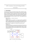
EITF35 - Introdution to Strutured VLSI Design (Fall 2015)
Course projets
v.1.0.0
1 Introduction
This document describes the course projects provided in EITF35 “Introduction to Structured VLSI Design” conducted at EIT, LTH. The projects are extensions to the lab assignments 2 and 3, where the ALU and PS/2 keyboard controller need to be integrated to
the whole system along with additional components. The basic requirement for projects
is that the result obtained by performing some functions such as addition, multiplication,
and other ALU operations is to be displayed on a computer screen interfaced to the FPGA
using the VGA port.
NOTE: Completion of project 1 gives a grade 4 and completion of both will result
in a grade 5.
Students interested in developing their own project to obtain a grade 5 instead of the
suggested project are welcome to discuss their proposals with the TAs. There are several
sensors on the Nexys 4 board which could be used to perform interesting projects. One
example would be to use the microphone or to use the accelerometers to implement a
simple video game.
2 Objectives
At the end of these projects the student will have learnt
• How to use the IP generator from Xilinx to instantiate IP cores
• How to perform fixed point programming and compare results from an algorithm
in Matlab with the output from the hardware design
• How to optimize code to obtain minimum area and hardware resource consumption
and how to meet hardware constraints
3 Assignments
* Project 1 - A calculator with memory:
Deadline Oct. 21
Instantiate an 8 kB, 8 bit wide RAM in your design using Xilinx IP generator. Integrate the keyboard, ALU, VGA controller and the newly created IP into your
design. The design should be able to input operands from the keyboard, store them
into the RAM and later calculate the result and display the result on the VGA.
1
* Project 2 - Integrated ALU with memory and a square root unit:
Deadline Oct. 30
The design should be able to get operands from the keyboard and store them in
the RAM. Along with performing the already implemented operations, the ALU
should be able to compute the square root of one operand with upto 3 decimal
digits in accuracy after the decimal point. The result should be displayed on the
seven segment display as well as the VGA screen. The square root unit should be
synthesized separately and should occupy less than 6% of the total number of slices
in the FPGA.
A typical block diagram for the top level with both project 1 and 2 integrated is
shown in Fig 1.
Figure 1: An overview on the course projects
Lab preparation
- Read this manual and try to understand the given tasks. Make sure that you have
understood what is expected from the projects. Consult the lab assistants, if the
functionality or any task is not expressed clear enough.
- Read the VGA section of the digilent Nexys 4 FPGA user manual, and go through
the provided VGA controller reference design. Understand how a VGA controller
works. Read about generation of IP cores using Xilinx IP generator.
Equipment
- A Digilent Nexys-4 FPGA board.
- A PC monitor with a standard VGA port.
- A PS/2 interfaced keyboard.
2
4 The VGA reference design
To ease the start of the project, a reference design of a VGA controller on the target
FPGA board is provided, where a course welcome message is loaded from FPGA’s block
memories and displayed on the monitor. The student can modify this design to suit the
requirements of whichever project he/she chooses to implement.
In both course projects, a VGA display with pixel resolution of 640×480@60 Hz
is used. The VGA port connections, VGA color signals and basic timing specification
may be found in the user guide of the FPGA board provided by Digilent. Therefore,
descriptions for these parts are not repeated in this manual, whereas only the VGA signal
timing diagram is illustrated here as shown in Fig. 2.
Video line
Horizontal
blanking
internal
Horizontal
blanking
internal
Horizontal
Synch.
25.6 us (640 clocks)
26.24 us (656 clocks)
30.08 us (752 clocks)
32 us (800 clocks)
Video
frame
Vertical
blanking
internal
Vertical
blanking
internal
Vertical
Synch.
15.36 ms (480 lines)
15.424 ms (490 lines)
15.744 ms (492 lines)
16.672 ms (521 lines)
Figure 2: Signal timing diagram for a 60 Hz, 640×480 VGA display.
To illustrate the use of the given signal timing information, a reference design of
the VGA controller is provided in this course and is briefly described in this manual.
The reference design displays a course welcome message on a VGA display, where the
message is saved as an image file stored in the block memories of the FPGA. An overview
of the provided VGA controller is shown in Fig. 3.
A) Clocking wizard (DCM) : This module divides the input clock frequency by a factor of 4, as the provided VGA controller is designed based on a system clock of
25 MHz. The clocking wizard is a primitive component available in Xilinx’s FPGAs, which may be generated from Xilinx Vivado environment with the use of IP
generator. The way of generating and properly configuring the Xilinx Clocking
wizard is shown as a video clip, placed under:
3
Figure 3: Block diagram of the VGA controller reference design.
“S:\tutorials\ise_clock_rom.wmv”,
NOTE: The video clip uses an older version of the IP generator, but the newer
Vivado tool makes it a lot easier. Several example videos can be found online
which describe the IP generator.
B) Picture ROM: This is the place where the welcome message is stored. The message
is saved as a bitmap image and is stored inside FPGA’s data ROMs. Data ROMs
may be generated with the use of Xilinx IP cores, however, the input data files have
to be loaded in a “.coe” file format during the ROM generation. This may be accomplished by using the software provided - “imageConverter”, placed under:
“S:\course_projects\imageConverter\”.
A bitmap image conversion is shown in a video clip “image_converter.wmv”, and
ROM generation is shown in “ise_clock_rom.wmv”, both placed under:
“S:\tutorials\".
C) VGA controller: This module contains two binary counters, used for tracking on
the horizontal video pixels and vertical video lines, respectively. Horizontal and
vertical synchronization pulses for the VGA display are generated based on the
counters, and an additional blank signal is provided as an output to indicate the
VGA blanking time interval.
D) Controller: The system controller keeps tracking on the current VGA pixel position
by using the horizontal and vertical counter values provided from the VGA controller. This module also controls the address of picture ROM, and reads out the
image data at the desired pixel locations. 3-bit color codes with one bit each for
red, green, and blue are sent to the VGA display, resulting in having 8 different
color tones.
Notice that physical pins mappings of the system I/O signals on an FPGA are accomplished with the use of a constraint file, namely the “.xdc” file, which is added in the
4
project structure.
5 Course project 1 (Grade 4) - A calculator with memory
In this project, the ALU implemented in lab assignment 3 and PS/2 keyboard controller
designed in lab assignment 2 will be reused. A new IP will be generated using the Xilinx
IP generator tool.
5.1 Task 1
Start by first understanding how the given VGA controller works. Try assigning your own
rgb colors to the display instead of ROM data. Figure out how the vertical and horizontal
counters can be used in order to emulate the seven segment display on the LCD. An illustration of the LCD display required is shown in a screen capture, placed under:
“S:\course_projects\rtl_ref_designs\project_1.jpg”.
Integrate the VGA controller to the keyboard and the ALU. Use a top level file to instantiate these three IPs as components in order to keep them functionally in separate
files. Reuse as much code as possible from your previous designs.
5.2 Task 2
In this step, you will generate your own memory module. The basic steps of generating
an IP core are listed below.
* Click on the IP Catalog in the Project Manager.
* Search for RAM. In Memories & Storage elements, choose RAMs & ROMs. Then
choose Block memory generator.
* In the new window that opens up, examine the memory block that will be generated.
* Choose a Single port RAM with the Algorithm set to Minimum Area.
* Set Memory write width to 8 bits and write depth to 8 kB.
* Leave all other options unchanged. Generate memory.
Once this is done, a new IP will appear in your design hierarchy window. Examine the
HDL files generated by clicking on + beside the IP and choosing the HDL files. The
component instantiation that needs to be used in your calculator design can be found in
this HDL instantiation file.
5
5.3 Task 3
Integrate the memory module into your design by instantiating it as a component and
verify that integration has succeeded. Refer to Fig 4 and the following steps for some
suggested ways to verify the memory controller. We will perform read and write operations to the memory using the basic pins and switches available on the board.
RESET
Latch Data
Latch Data
Increment
Address
Increment Address
Address UP/Down
Figure 4: FPGA with memory controls
* Assign CPU RESET to reset your system. Check whether the reset is active high
or low and make appropriate changes to your code. If you have a different polarity,
instead of changing the whole code, you can create a local reset signal with the
required polarity in your top level and use this as the reset for the rest of your
system.
* Even though the mem_data bus generated from the IP will be 8 bits, for testing we
will now use only 4 bits. Assign the mem_data[3 downto 0] bits to your keyboard
out data. Assign the upper 4 bits to zero.
* Design a counter and connect the mem_address to this counter. When BTNL is
pressed and if SWITCH[12] is set to 0, the address should increment. The address
6
should decrement if BTNL is pressed when SWITCH[12] is set to 1. Remember to
use debouncing logic on the BTN, if not the memory address might increment by
more than one at each press of BTNL. It would be a good idea to also connect the
mem_write_enable to this button.
* Try and use the LED0-7 present on the board for debugging. Check whether after
adding debouncing logic the address increments by the required steps.
* Assign BTNC to enable data latching. The keyboard data should be registered to
the memory input only when BTNC is pressed.
* Connect the memory_out data to the seven segment display, either on the FPGA or
on the LCD screen for debugging.
It is always a good idea to look at the warnings tab when synthesizing the design.
Understand the warnings shown and see if they are OK for your design. It may happen
that the memory block is not connected properly and your system does not work.
5.4 Task 4
The next step is to write code to enable data storage in the memory along with the operators. Use the same BTNC-BTNL logic described above to store a string of data into the
memory along with the operands. The input data range is from 0 to 255 and the inputs are
considered to be unsigned. At the end of entering data values along with operands, the
ALU should be started. This can be done by pressing the <Enter> key on your keyboard.
A) At the press of every <Enter> key the memory controller should be able to pop the
top three memory locations (the two data operands and the operator), compute the
result and display it on the VGA screen.
B) On the next <Enter> key the next two data operands and the operator have to popped
out from the memory and result should be displayed on the VGA screen. Do not
forget to take into account that for the mod 3 operator we need to enter only one
data and the operand. Remember also that the result could be either a positive or a
negative number. Therefore it is required to display the sign of the result before the
result as shown in the example in Fig. 5.
C) Since the data RAM created will be 8 bits wide and we need to store some operands
along with data, some of the bit patterns can be assigned for these operators(e.g.
“+”, “-”, “=” “mod”). Choose the range of 130 to 135 for operators. This also
means that input data in the range of 130 to 135 shall not be considered as operands.
D) The values should be stored into the RAM only when proper operands and operators
have been entered. There should be an option to use the back space key to input
a different set of operators and operands. For example, if a mistake is done while
entering the operands, one could use the backspace key to delete the already entered
numbers and start over. A detailed description of operators and operands is as
follows:
7
E) Both data operands must be displayed in at least 3 digits (hundreds, tens, units) on
the VGA screen and the computation results must also be represented in three digits
(hundreds, tens, units) along with the sign. The operands, computation result along
with the operator must be shown on the emulated 7-segments on a VGA monitor.
For example if one has to compute the sum of 98 and 99 the VGA display should
look like the ouput in Fig. 5. The inputs will be entered in the 3 digits format,
meaning if one wants to use 9 as an operand, the input from the keyboard shall
be 009. If the data entered is above the limit, then the number shall be stored as
255. For example if the user enters 1234 as the first input operator, the calculator
shall store this number as 255 when the data latch button is pressed. Note that the
backspace key should be operational to fix the data before the data latch button is
pressed.
F) If you plan on performing project 2, consider that the maximum width of the result
displayed on the monitor should be 5 digits, which corresponds to the square root
of 255 = 15.968.
Figure 5: Example VGA Output
Remember that the result is signed and the operands are unsigned. This will enable
one to design a simple state machine to accept the right amount of inputs before
storing them in the memory.
G) The design must be able to perform the following different computation operations:
addition, subtraction, multiplication and modulo 3. An indication of overflow/underflow should also be displayed when it happens.
H) The emulated 7-segments have to be shown in a visible size. It is allowed to load
digits and operators from data ROMs, however, you have to consider the available
memory capacity in the FPGA. It is recommended to design a display engine for
one 7-segment, and use it to generate digits at all locations during system run-time.
Using either logics or data memories is always a design trade off, where a common
practice is to use a mixed design approach to find a balanced point between them.
You may, for instance, store all data operators (e.g. “+”, “-”, “=”) in ROMs, and
generate all digits by using one 7-segment display engine.
An example output of the memory operation is shown in Fig 6. Refer to the presentations uploaded along with this manual for details on how to fill in the memory and reading
the memory. To begin with, the write address is “0". When data and operands are entered,
the memory will fill up in a way similar to a stack. Once the user decides to compute the
results, the <Enter> key will be pressed. This should result in popping data from the top
of the stack and displaying results on the VGA screen. Further <Enter> keys should pop
data correctly in order to display the corresponding result. The calculator should also be
8
able to accept data inputs in the middle of displays. For example in Fig. 6 after the third
<Enter> key has been pressed resulting in a display of +049 on the VGA monitor, the
user should be able to input more operands and operators. This should result in the memory being filled up again until the user decides to evaluate the results using the <Enter>
key. Contact the teaching assistant if you have any questions on the operation of the
memory.
Initial position
Direction of POP
Direction of memory fill
(similar to a stack)
13
%
10
*
0
7
*
7
On first enter key
013%003 = +001
On second enter key
100*000 = +000
On third enter key
007*007 = +049
On fourth enter key
006-030 = -024
On fifth enter key
003*054 = +162
On sixth enter key
098+010 = +108
6
30
3
*
54
98
+
10
Figure 6: Example output
9
6 Course project 2 (Grade 5) - ALU with square root and
Memory
In this project an additional operation namely the computation of the square root of an
unsigned number will be added to the ALU. The computed result should be displayed on
the emulated seven segment display on the VGA monitor with upto three decimal digits
in accuracy. The detailed requirements are as follows
A) Interface the keyboard, ALU and the VGA as explained in the previous sections.
Emulate a seven segment display on the VGA screen.
B) The square root unit is to be designed which should accept an unsigned integer
as its input and produce the square root of the number with at least three digits in
accuracy after the decimal point. The input range for the square root number will be
[0-255]. The square root unit has to be integrated into the ALU. The design should
be capable of accepting data from keyboard, compute results for different operands
like addition, multiplication and square root, then display the result on the VGA
screen. You can assign the key of your choice to perform the square root, such as
the ‘s’ button from the keyboard.
C) Find an algorithm to calculate the square root or use the algorithm such as the
Newton-Rhaphson method. An introduction to algorithms implementing square
root can be found on Wikipedia. Use a lookup table to find the closest square root
and start with that as the seed to the algorithm. Several iterations can be done to
obtain a reasonably accurate square root of a number with Newton’s method.
D) Start by writing a Matlab script which uses the fixed point (fi) notation tool. Understand what widths of inputs and outputs are required to produce the desired
accuracy in the final result. Think about number of bits needed by the divisor and
choose correct widths appropriately.
E) Discuss the algorithm implementation and the bit widths that you have chosen with
the TA.
F) The final implementation of the square root unit should be able to fit inside 6%
of the total number of slices.
G) You will probably need a divider unit to perform the square root algorithm. Instantiate a divider core generator IP from the IP generator tool. Select the algorithm
to be of type “fixed” with dividend and divisor widths to be of X and Y bits respectively. The values of X and Y should be obtained from Matlab simulations or
by calculations. Since you need 3 decimal digits of accuracy, this would probably
correspond to a fraction binary width of 10 bits.
H) Read the divider IPs manual to understand the number of cycles it takes to produce
one division output. Construct a small testbench and verify that you understand the
divider’s operation.
10
I) The next step is to design the algorithm and integrate it into the system. From
simulations done in Matlab you will be able to understand the number of iterations
required to reach the desired accuracy for all the numbers in the range from [0-255].
Once this is fixed, design a state machine which will start when lets say BTNC is
pressed and process the square root of the input number. For testing purposes, you
can input the number from the SWITCH buttons. Remember to wait for the division
operation to complete before proceeding to the next iteration. Construct a testbench
and verify that the state machine is functioning as required. The divider IP returns
the integer and fractional part of the quotient. Make sure you design your adders to
take care that the fractional bits are added correctly and the integer bits are updated.
J) The final result obtained will contain an integer part and a fractional part. The
integer part and the fractional part needs to be displayed as a BCD number. Design
a small function to do this.
K) Integrate the square root unit to the ALU with memory designed in Project 1. The
final result should be displayed on the CRT monitor using the VGA controller and
the input should come from the keyboard instead of the SWITCH keys.
L) Remember to do things step by step. Create modules based on functionality and
integrate in the top level. For example, you should have a separate module which
accepts a seven segment coded number and displays on the VGA, one separate
module to perform square root, one to do all the other ALU operations etc.
11