1
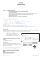
EE254L
Divider design
Objective: To introduce to students
-- RTL coding style for state machine and datapath coding
-- Testbench with a “task”
-- debouncing mechanical Push Buttons and generating DPB, SCEN, MCEN, CCEN
-- Single-stepping and Multi-stepping using the push-button debounce unit
-- Introduce Epp protocol
-- Exploit the I/O resources in Adept 2.0 I/O Expansion
References (for the TAs, not for students):
1. Nexys-3 board reference manual (Nexys3_rm.pdf) and schematic
http://digilentinc.com/Products/Detail.cfm?NavPath=2,400,897&Prod=NEXYS3
http://digilentinc.com/Data/Products/NEXYS3/Nexys3_rm.pdf
http://digilentinc.com/Data/Products/NEXYS3/NEXYS3_sch.pdf
2. Epp protocol
First 4 pages of the Digilent Parallel Interface Model Reference Manual
http://www.digilentinc.com/Data/Products/ADEPT/DpimRef%20programmers%20manual.pdf
Files provided:
A zip file is provided containing source files for four sample designs in four folders. Please read the notes
at the top of each file to get to know important aspects of the design to note.
1. ee254_divider_simple
2. ee254_divider_with_debounce
3. ee254_divider_with_single-step
4. ee254_divider_with_VIO_multi_step
Extract from divider_combined_cu_dpu.v
A short description of each of the above 3 designs
follows.
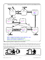
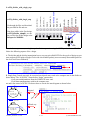
3. ee254_divider_simple:
Points to note:
The datapath elements shall be inferred by the synthesis tool. So we do not code OFL explicitly. See the
diagram on the next page.
LD7
SW7
LD0
SSD3 SSD2 SSD1 SSD0
BtnU
SW0
BtnU
BtnL
The datapath and the control unit can be combined in
one case statement under clock as shown in
divider_combined_cu_dpu.v. Notice the lines on
the side which avoid unnecessary recirculating
muxes.
We have also provided another file:
divider_separate_cu_dpu.v.
EE254L_divider.fm 7/19/14
1 / 15
BtnR
BtnL
BtnC
BtnD
BtnD
BtnR
BtnC
BtnC
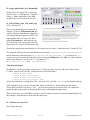
(C) 2014 Gandhi Puvvada
Division between DPU and
Traditional division
CU for HDL coding
between DPU and CU
I0
Y
I1 S
Y_Reg
I0
Y
I1 S
Y_Reg
I0
Y
I1 S
X_Reg
DPU
I0
Y
I1 S
X_Reg
OFL (combinational logic)
is moved to DPU. It is
NOT coded explicitly.
The OFL is implicit in the
DPU’s RTL in the CASE
statement.
DPU
OFL (combinational logic)
is in the CU.
OFL
NSL
OFL
SM
Current_State
NSL
SM
Current_State
CU
BtnC
REMINDER
QUOTIENT
ACK
DIVISOR
DIVDND
BtnL
BtnR
ACK
DIVISOR
BtnU
START
DIVIDEND
RESET
START
BtnD
BtnR(ACK)
BtnU
BtnL(START)
DONE
Qd (DONE_S)
Go through the files and download
the provided bit file and test.
Qc (COMPUTE)
ee254_divider_simple
Qi (INITIAL)
CU
BtnC
BtnD
RESET
Questions for the ee254_divider_simple design:
A. What happens if you divide by zero? Is the behavior of the quotient digit display on SSD1 different if
you attempt to divide 3 by 0 vs. if you attempt to divide F by 0. How about 0 divided by 0?
B. If you improve the divider design to move from compute state to done state if X is equal or less than Y
(instead of the current X less than Y), will the above behavior change? Does your answer to Q#1 above
change?
C. Why does the behavior of the next design (ee254_divider_with_debounce) appear to be quite different
from this design for division by zero? Is it just appearance only or is it really different? Note: Look at the
rate at which sysclk runs in both designs
EE254L_divider.fm 7/19/14
2 / 15
(C) 2014 Gandhi Puvvada
4. Bouncing of mechanical Switches and Push Buttons:
BtnU
VCC = 5V
VCC = 5V
BtnL
OPEN
SW
BtnR
OPEN
10K
High when
SW is ope
SW
Low when
SW is open
BtnD
10K
Works for TTL and CMOS logics
BtnC
(C for Center)
Works for CMOS but not TTL logic
Buttons on Nexys-3:
When pressed, they produce high.
PB
0.084s
0.084s
DPB
SCEN
5. Debouncing State Machines:
Debouncing State Machine (To start with just produce DPB and SCEN)
PB T=0.084
PB
RESET
INI
WQ
PB
I <= 0;
PB
SCEN_St
I <= 0;
DPB = 1
SCEN = 1
1
CCR
PB
DPB = 1
I <= I + 1;
PB
PB T=0.084
PB
T=
WFCR
0.0
84
I <= I + 1;
PB T=0.084
I <= 0;
DPB = 1
PB = Push Button
PB =1 => Push Button pressed
PB
WQ = Wait for a Quarter Second (actually 0.084ms)
SCEN = Single Clock Enable
(enable the RTL transfer operation and/or state transfer operation for one clock of the 100 MHz system clock)
CCR - Clear Counter
WFCR = Wait For Complete Release
DPB = 1 in all states except for INI and WQ states.
SCEN = 1 in SCEN_St only. Hence SCEN is a single-clock wide pulse.
EE254L_divider.fm 7/19/14
3 / 15
(C) 2014 Gandhi Puvvada
Debouncing State Machine (Now produce MCEN and CCEN besides DPB and SCEN)
PB T=0.084
PB
RESET
INI
WQ
PB
I <= 0;
I <= I + 1;
PB
PB T=0.084
PB
T=
WFCR
0.0
84
I <= I + 1;
1
DPB = 1
PB
PB T=0.084
SCEN_St
I <= 0;
DPB = 1
SCEN = 1
MCEN = 1
CCEN = 1
CCR
1
I <= 0;
DPB = 1
PB
PB
CCEN_St
MCEN_St
1
I <= I + 1;
I <= 0;
PB T=0.084
WH
PB T=0.168
I <= I + 1;
DPB = 1
DPB = 1
DPB = 1
MCEN = 1
CCEN = 1
CCEN = 1
PB T=0.168
PB T=0.084
MCEN = Multiple Clock Enable (of course with 0.084 sec. gap)
CCEN = Continuous Clock Enable (with no gap)
MCEN is active in SCEN_St and MCEN_St.
CCEN is active in SCEN_St, MCEN_St, and CCEN_St states.
6. How to produce glitch-free outputs from a state machine:
Earlier, in class, we showed how easily glitches are produced by a combinational logic such as a mux or an
equality checker. If we can avoid the OFL (Output Function Logic) in a Moore kind of state machine by
cleverly coding symbolic states using output coding, then the output control signals come out of state flipflops and they will be glitch free!
NSL
SM
NSL
OFL
PI
SM
PI
DNS
CS
DNS
CLK
CS
Original State Machine with OFL
EE254L_divider.fm 7/19/14
CLK
Output-coded State Machine with no OFL
4 / 15
(C) 2014 Gandhi Puvvada
7. ee254_divider_with_debounce:
Let us go through the debouncer design, ee254_debounce_DPB_SCEN_CCEN_MCEN.v. It debounces a
given push button and produces 4 outputs: DPB, SCEN, CCEN, MCEN.
Output coding (for the states in the state machine) is used to produce glitch free outputs.
TB1 and TB0
are the tie-breakers
to break aliasing in
output codes.
One more state added
to improve the utility
of the earlier MCEN.
ISE => Help => Software Manuals => Click on
Design Synthesis in the diagram (copy shown on
the side) => XST User guide => Search for FSM
Encoding
As shown here, we used verilog attributes to
enforce our output coding. Through these attributes,
we are informing the tool-vendor (Xilinx here) that
we want the tool to honor and retain our user encoding.
It is possible to set FSM Encoding option under
ISE => Synthesis XST => Properties => HDL
options => FSM Encoding Algorithm = User.
But this will apply to the entire design!
Verilog attributes are placed in parentheses
between asterisks. Another example:
EE254L_divider.fm 7/19/14
5 / 15
(C) 2014 Gandhi Puvvada
Read the code (ee254_debounce_DPB_SCEN_CCEN_MCEN.v) and complete the state diagram on the
next page. Simulate it using ee254_debounce_DPB_SCEN_CCEN_MCEN_tb.v for 9 us.
Notice that, the testbench
has instantiated the UUT
with N_dc of 4 in the
generic map
#1
#2
8 pulses? Shouldn’t they be six?
#3?
BtnL
BtnC
REMINDER
QUOTIENT
DIVISOR
DIVDND
BtnU
BtnR
START/ACK
DIVISOR
START/ACK
DIVIDEND
RESET
Note that, unlike in the earlier design,
(ee254_divider_simple), we run
the core divider in this design at the
full speed of 100Mhz.
BtnD
BtnR
BtnU
(START/ACK)
BtnL
DONE
Qd (DONE_S)
Go through the files and download
the provided bit file and test.
Qc (COMPUTE)
ee254_divider_with_debounce
Qi (INITIAL)
A simple (rather construed) example of the SCEN pulse of debouncer is as follows. Suppose, we are running short of the buttons on the board and we wish to use a single button (BtnL) both as a START button
and an ACK button, Then DPB pulse does not help as our divider is running at full speed (100MHz) and
one operation of the BtnL (say 0.2 sec) will be considered as several hundred thousands of these START
and ACK operations. So when you let the BtnL go, you can not tell whether the state machine is waiting in
the Initial state or Done state! But with SCEN, only one-clock wide pulse per operation is applied to the circuitry!
BtnC
BtnD
RESET
Questions on the debouncer and the divider with debouncer:
1. Briefly explain why the N_dc parameter was changed to 4 during simulation (from the actual value of 25
for synthesis and implementation). Use words such as “inefficient”, “wasteful”, “readability of waveform”,
etc.
2. When you simulate, zoom into the area of above waveform extract and arrive at your answer for the
above question in the waveform extract (why do we see 8 more pulses on MCEN after already seeing two
pulses.
3. Did we use the DPB (Debounced Push-Button) pulse or SCEN (Single-Clock enable) pulse to act as the
Start signal and the Acknowledge signal? Could we have used anyone of them?
EE254L_divider.fm 7/19/14
6 / 15
(C) 2014 Gandhi Puvvada
Complete the Debouncing State Machine with the added state MCEN_cont
Complete the missing state transition conditions and also any RTL in the state MCEN_Cont
PB T=0.084
PB
RESET
INI
WQ
PB
I <= 0;
PB T=0.084
I <= I + 1;
PB
SCEN_St
I <= 0;
DPB = 1
SCEN = 1
MCEN = 1
CCEN = 1
MC <= 0;
MC <= MC + 1;
PB T=0.084
PB
T=
WFCR
0.0
84
I <= I + 1;
1
DPB = 1
PB
CCR
I <= 0;
1
Note
DPB = 1
MC <= 0;
PB
CCEN_St
MCEN_St
1
I <= 0;
I <= I + 1;
DPB = 1
DPB = 1
MCEN = 1
CCEN = 1
CCEN = 1
WH
PB T=0.168
I <= I + 1;
DPB = 1
MC <= MC + 1;
PB T=0.168
MC stands for MCEN count.
After certain count of MCN,
control is transferred to
MCEN_Cont.
count[0]
MCEN_Cont
count[1]
count[2]
MCEN_Continuous state
count[3]
Here MCEN behaves like CCEN.
See the output coding table given before.
count[3] becomes 1 after 8 (=23) clocks of the CLOCK.
count[23] becomes 1 after 223 clocks of the CLOCK.
223 clocks each of 10 ns make 0.084 sec. Hence T1 = 0.084 sec
224 clocks each of 10 ns make 0.168 sec. Hence T2 = 0.168 sec
Names of the students submitting:
Nexys3 board clock is at 100MHz.
100MHz frequency corresponds to 10ns clock period.
1.
2.
EE254L_divider.fm 7/19/14
7 / 15
(C) 2014 Gandhi Puvvada
8. Single-stepping:
Single-stepping and break-point setting are used in software or hardware debugging. Here we wish to show a
hardware debugging mechanism involving single-stepping and multi-stepping, which will lead to setting break
points. This will be useful particularly when you are interfacing your design with an external system which can
not be simulated and proven in simulation. Also sometimes there will be simulation/synthesis mismatches and
this helps in debugging in those situations. In later labs, we will also show you chipscope to gather hardware
signal activity at full speed. Chipscope is essentially a logic analyzer placed inside the FPGA chip to sample
and gather signals and show them to us on the PC monitor as waveforms or state listings.
Let us first talk about single-stepping. Most common idea is to apply one clock pulse at a time whenever the
single-step PB is pressed. One can think of using a clean (glitch-free) pulse such as DPB as the clock to the
system. However the problem in FPGA is to put this derived clock on global routing resources in FPGA.
Spartan-6 FPGA Clocking Resources
http://www.xilinx.com/support/documentation/user_guides/ug382.pdf
If we can not use the global routing resources for our DPB, then this
DPB reaches different registers in our design at different times and the
D
Q
relative skew (difference in the arrival times of these clock pulses)
CLK
causes the circuit to fail. For example consider a simple right-shift regisCLK
SCEN
ter, with progressively delayed clock sent to the right-side flip-flops.
CLK
Multi-stepping occurs and the shift register fails. Hence we designed a
SCE
better way to implement single-stepping. We do not use DPB or SCEN SCEN with
glitches
as “the clock” but we use SCEN as the clock enable. SCEN stands for
Single Clock Enable and it is nominally equal in width to a single clock
cycle. Since it is the clock enable and control the data-recirculating mux, even if SCEN has some glitches, they
do not hurt the circuit operation. The glitches are in the beginning of the clock and die down by the end of the
clock. It is the responsibility of the STA (Static Timing Analyzer, which is part of any synthesis tool) to make
sure that the glitches die down before the arrival of the next clock-edge. So, if the circuit passed timing-design,
we can be assured that the glitches do not hurt our circuit.
I0
Y
I1 S
Single-stepping is not a complete solution for debugging as very often, we need thousands or millions of
clocks needed before the suspected malfunctioning part of the circuit behavior can be encountered. For example, a real-time clock (a wall-clock) may misbehave at the roll-over from 23:59:59 to 00:00:00. So, it is a good
idea to produce MCEN and CCEN. We can easily modify the above state diagram to terminate the CCEN or
MCEN to force the debounce state machine go back to initial state under any break-point condition (such as
time = 23:59:59).
EE254L_divider.fm 7/19/14
8 / 15
(C) 2014 Gandhi Puvvada
Note that, unlike in the first design,
(ee254_divider_simple), we run
the core divider in this design at the
full speed of 100MHz.
REMINDER
QUOTIENT
DIVISOR
DIVDND
BtnD
BtnR(ACK)
BtnU(SINGLE-STEP)
BtnL(START)
DONE
Go through the files and download
the provided bit file and test.
Qd (DONE_S)
ee254_divider_with_single_step
Qc (COMPUTE)
Qi (INITIAL)
9. ee254_divider_with_single_step
SINGLE-STEP
DIVISOR
BtnL
BtnU
BtnC
ACK
DIVIDEND
START
SINGLE-STEP
BtnR
BtnC
BtnD
RESET
Here, in the compute state, we single-step the division operation using the SCEN produced out of BtnU.
Notice the following aspects of the design.
A. The divider and the divider instantiation have a new port pin called SCEN for the top-level design to generate and pass SCEN pulses (Single-Clock-wide clock enable pulses) (more accurately data-enable pulses as
the clock itself is not inhibited).
B. Single-Step Control can easily be exercised on selected states such as the compute state in the divider as
shown below. The “if (SCEN)” clause before “begin” ensures that
(i) all state transformations from the COMPUTE state and
(ii) all data transformations with-in the compute state,
are under the control of SCEN. We do not have to rewrite the state diagram as shown below.
X
>=
Y
COMPUTE
if X >= Y
X <= X - Y;
Q <= Q + 1;
X
Original
<
Y
Ea
sy
W
ay
SCEN + (X >= Y)
Difficult way
COMPUTE
if (X >= Y) . SCEN
X <= X - Y;
Q <= Q + 1;
SC
EN
EE254L_divider.fm 7/19/14
.(
X<
Y)
9 / 15
(C) 2014 Gandhi Puvvada
Questions on ee254_divider_with_single_step:
B. Can we choose to place all three states of the divider design under single-stepping control and simultaneously combine Start and Ack under one button (say BtnL)?
Is this just not possible or it works if we produce a BtnL_ SCEN and use it as START as well
as ACK, or ...?
Can you press two buttons exactly at the same time to 10ns or 5ns accuracy? Even if you
press at the same time to that accuracy, can you guarantee that they bounce for the same
length of time and the two instances of the debouncing state machine would produce their
respective SCEN pulses at the same time?
START/ACK
A. Is it possible to use SCEN to control one state (or a few states), MCEN to control another state, and further
CCEN to control yet another state? When we say “control a state” here, we mean control the RTL operations in
the state and also the state-transitions going away from the state (excluding looping-around state transitions). If
we are not going away from the state (because of absence of the SCEN pulse) then we will remain in the state,
whether originally there is a loop-around state-transition or not.
BtnL
SINGLE-STEP
BtnU
BtnC
BtnR
BtnC
BtnD
RESET
C. We took time to design output-coded state machine with no OFL at all, there by avoiding any glitches in the
SCEN, MCEN, etc. Are glitches really harmful in our design or we have just shown a way to produce glitchfree outputs?
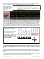
10. Epp Interface on Nexys-3 board for communication with the PC
EE254L_divider.fm 7/19/14
10 / 15
Spartan 6 FPGA
Cypress USB
interface chip
Epp stands for Enhanced Parallel Port. Epp interface was
used to interface PC-XT to a dot-matrix printer in 1980’s.
Epp
(http://en.wikipedia.org/wiki/IEEE_1284). It is a very simple
CY7C68013A
interface and easy to use though obsolete. Since USB interface is a fairly complex interface, and since current PCs do
Nexys-3 Board
USB
not support Epp interface, Cypress (http://www.cypress.com)
PC
Cable
offer USB interface chips, which convert the USB interface to
simple interfaces such as Epp. Since Epp is a very simple
interface, Digilent chose to use a Cypress interface chip
CY7C68013A on their Nexys-3 boards to convert communications from and to a PC on USB to Epp for us to deal with on
the FPGA. Digilent has also provided the Adept software to
run on the PC and communicate with the Cypress chip on
USB. They have also provided IOExpansion.vhd (which we
translated to Verilog for EE254L as IOExpansion.v) for
instantiation in FPGA-side designer’s top file. The UCF file
for such project should include the pins associated with the
Epp interface. On the Adept GUI, the Register I/O, the File I/
O and the I/O Ex. Here, in this lab we explore the I/O Ex tab,
which we refer to as Virtual I/O. We call it Virtual I/O as it
adds several addition Switches, Push Buttons, LEDs on the
GUI to the limited number of these on the Nexys-3 board. Besides these, we can exchange 32-bit data using the
two boxes labeled as “To FPGA” and “From FPGA”. After instantiating the IO Expansion module (defined in
IOExpansion.v), the user logic can send data to the LEDs in the I/O Ex tab very much in the same fashion as he
would send data to the LEDs on the Nexys-3 board. He can read from data on the Virtual switches very much
like he reads switches on the Nexys-3 board. The Adept GUI uses program driven I/O (not interrupt driven I/O)
to exchange data. It sends and receives data very frequently.
(C) 2014 Gandhi Puvvada
A short extract from Digilent manuals:
Net
Net
Net
Net
"EppAstb"
"EppDstb"
"EppWait"
"EppWr"
LOC
LOC
LOC
LOC
=
=
=
=
H1
K4
C2
F5
Some of the
Epp pins in
the .ucf file.
(The Address Read perhaps is not used in Adept software)
Instead of viewing this as a low active wait, it may be easier to view it as a high-active GOT signal.
Notice that the Epp protocol implements the full (4-way) handshake.
Nexys-3 Board
Spartan 6 FPGA
divider_top
IOExpansion.v
(from IOExpansion.vhd)
EppDstb
EppWr
8 EppDB
regEppAdr
EppAstb
Cypress USB
interface chip
PC
USB
Cable
#1
#2-4
#5-6
Sw
EppWait
EppWr
#7-8
Btn
#9-c
dwOut
#0d-0f,10
#0
regVer
EE254L_divider.fm 7/19/14
11 / 15
Led[7:0]
Lbar[23:0]
Sw[15:0]
Btn[15:0]
dwOut[31:0]
dwIn[31:0]
divider_combined_cu_dpu_with_VIO_multi_step.v
File: divider_top_with_VIO_multi_step.v
(C) 2014 Gandhi Puvvada
11. Epp Protocol in short
64Kx8
(
1 Take it 2 Got it
3 I see you got it 4 I see that you saw that you got it
A15-A0
D7-D0
de
A19-A16
co
de
r
Intel
8088
RD
used in
OE
WE
WR
PC-XT
CS
D7-D0
EppAstb
EppDstb
Epp Slave
Epp Master
Let us understand a simple processor to memory interface.
The processor puts out address and a control strobe (RD or WR)
and exchanges data with the addressed location in memory.
But this involves several signal wires. In the case of (simplified) 8088 to memory interface, we need 20 address lines
(A19-A0), 8 data lines (D7-D0), two control strobes (RD and
WR). In the case of Epp, it is desired that the interface has less
wires. So instead of separate address lines and separate data
lines, Epp uses one set of 8 data lines which carry data if Dstb
is active and address if Astb is active. Since these strobes
carry timing information also, we do not need the strobes to
carry timing information. Instead, in Epp, we have WR line,
which can be viewed as indicating the direction of transfer (WR
= 0 means write and WR = 1 means read). In microprocessormemory interface, we have a READY line (not shown on the
side) which allows a slow memory to request for more time to
respond. Here we have Wait to implement a 4-way handshake
protocol
A15-A0
A15-A0
EppWr
8 EppDB
EppWait
).
3
1
How does the Epp protocol provide for multiple data transfers
in the absence of an address bus?
The Epp master can convey an address first using DB[7:0] and
Astb and then later data using DB[7:0] and Dstb for that
addressed location. Oh, it means we can at most exchange 256
bytes because using 8-bit address you can only generate 28 =
256 addresses! No, it is not like that. The Epp master and the
Epp slave can have a common understanding that the master
always sends address in two parts, high part followed by low
part before data is transmitted. This increases the number of
bytes that can be transferred to 64KB (216 = 65536 = 64K).
= GOT
4
2
4
Extract of
IOExpansion.v
Epp Address Register is written
at the end of the Epp Address Strobe
because Epp Write control line is
low indicating intent to write.
Adept 2.0 or higher running on your PC control the Cypress interface chip and causes communication
between the Adept GUI on your PV display and the Cypress chip.
The Cypress chip is the Epp master, which drives the three control lines:
EppAstb: Epp Address Strobe (active low, ending edge is posedge),
EppDstb: Epp Data Strobe (active low, ending edge is posedge),
EppWr: Epp Write Control (active low, low means intent to write, high means intent to read).
The EppDB is the Epp 8-bit data bus. During an active address or data strobe, Epp master drives data
if write is true (EppWr = 0) else slave drives data if read is true (EppWr = 1).
Active-low WAIT (= active-high GOT) acts like a hand-shake signal between the two parties.
Address Read Cycle is not implemented in Adept Virtual I/O protocol.
EE254L_divider.fm 7/19/14
12 / 15
(C) 2014 Gandhi Puvvada
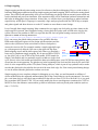
12. Adept Application User's Manual.pdf
Please refer to the Adept User’s manual on
your PC (Start => All Programs => Digilent =>
Adept => Adept Application User's Manual.pdf. Extract of it is shown on the side.
13. ee254_divider_with_VIO_multi_step
(VIO = Virtual I/O)
Here we are interfacing to the virtual I/O in
Adept 2.0. The file, IOExpansion.vhd, provided by Digilent, implements the Epp slaveside address and data registers in FPGA. We
translated the same to Verilog. The file is
called IOExpansion.v. Note that now, the
UCF file needs to have pins associated with
Epp to talk to the Cypress USB interface chip.
The next two pages show the utilization of I/O resources on the Nexys-3 board and in the Virtual I/O GUI.
One important difference between the debouncer user earlier (ee254_debounce_DPB_SCEN_CCEN_MCEN.v)
and the debouncer used in this part (ee254_debounce_DPB_SCEN_CCEN_MCEN_r1.v) is that here (in _r1
version), we have increased the time gap between consecutive MCEN pulses to 1.342 sec. Hence instantiations of the debouncer uses here an N_dc parameter of 28:
ee254_debouncer #(.N_dc(28)) ee254_debouncer_2
Task to be performed
Download the .zip file provided to you into your C:\xilinx_projects\ directory and extract files to form
C:\Xilinx_projects\ee254_divider_verilog directory with 4 sub-folders:
1.
2.
3.
4.
ee254_divider_simple
ee254_divider_with_debounce
ee254_divider_with_single-step
ee254_divider_with_VIO_multi_step
All the four folders have verilog source files, .ucf source file, a .bit file (with TAs_ prefix) of the completed design
.
After reading the code, you can download the .bit file to the Nexys-3 board and operate the divider.
The bit files provided to you have a “TAs_” prefix so that you do not overwrite when you compile the
sample designs to get practice in forming a xilinx project and implementing the same.
When you are done, you will submit a report to your TA with your answers to questions posted under first
three designs. No questions are posted for this last design.
14. Celebrate your success!!!
Don’t forget this step!
EE254L_divider.fm 7/19/14
13 / 15
(C) 2014 Gandhi Puvvada
Adept Virtual I/O resource utilization for this part of the lab (unused resources are crossed out):
ee254_divider_with_VIO_multi_step
Multiplexing the two displays on the
four 7-seg displays using Btn1.
DIVIDEND
DIVISOR
QUOTIENT REMAINDER
Go through the files and download
the provided bit file and test.
when btnR is not pressed
when btnR is pressed
BtnD
START/ACK
The switches on the board
are not used here.
8-bit dividend and 8-bit
divisor are set using the
16 switches on Adept IOExpansion.
BtnL
MULTI-STEP
BtnU
DISPLAY
SELECT
START/
ACK
Multi-Step
DONE
Qd
Qc
Qi
DISPLAY
SELECT
BtnC
BtnR
BtnC
RESET
BtnD
BtnD
BtnC
Order of Buttons:
BtnL
BtnR
BtnC
BtnD
RESET
RESET
BtnC
BtnD
BtnU
BtnR
Display Select
BtnC
MULTI-STEP
BtnL
START/ACK
BtnU
MULTI-STEP
DISPLAY
SELECT
START/ACK
The push button mapping is as follows:
Though not
used in this lab
BtnL, BtnU, BtnR, BnD, BtnC
EE254L_divider.fm 7/19/14
14 / 15
(C) 2014 Gandhi Puvvada
In this example 58H is the dividend and 04H is the divisor.
The quotient is 16H and the remainder is 00H.
{8{BtnR_combined}};
Can be used to send the Dividend (Xin) and the Divisor (Yin)
Dividend, Divisor, Quotient, Remainder
assign lbar_to_VIO[7:0]
=
Qd Done
Replica of Nexys-3 LEDs
Can be used to set Dividend
of Nexys-3 Buttons
box.
START/ACK
Note: The 16 switches shall be in down (off)
position, if you want to send Xin, Yin via the
Replica
facility. Similarly, if you want to
use the switches to send Xin, Yin, send 0x0 through the
Light Bar when not lit
BtnL
Btn U
Btn L
EE254L_divider.fm 7/19/14
15 / 15
MULTI-STEP
BtnU
DISPLAY
SELECT
Can be used to set Divisor
assign {Ld3, Ld2, Ld1, Ld0} = {BtnL_combined, BtnU_combined, BtnR_combined, BtnD_combined};
ee254_divider_with_VIO_multi_step
BtnC
BtnR
BtnC
Btn R
BtnD
RESET
(C) 2014 Gandhi Puvvada