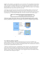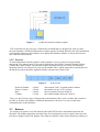
1
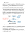
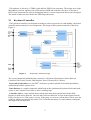
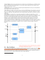
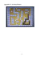
Find Pennies GAme
2012-10-25
Emil Selinder, [email protected]
Daniel Lehtonen, [email protected]
Fredrik Johnson, [email protected]
1
Abstract
? is this a sequel from the proposal?
This project will be about implementing a game on the Digilent Nexys 3 FPGA-board. The game
is called Find Pennies GAme and the objective is to guide a character through a maze and collect
coins. When the character moves from one floor-tile to another, the floor-tile will disappear behind
the character, which means you will have to plan your path carefully.
The game is implemented using both hardware and software components. The hardware part is
specified using VHDL and the software is written in C. The hardware consist of components
storing the graphics and the matrices containing the details on how the output to the VGA should
be built. There is also a controller for the VGA that controls the counters and the output signals
using the matrices stored in the custom made components and logic for storing the values from the
on-board buttons. These buttons were mainly used since the keyboard controller written did not
synthesize as expected, which is a problem we will discuss later in the report.
The software components were fairly simple and the main objective of the software is to run the
actual game that was implemented as well as read input from the button registers and decode these
into proper outputs for the matrices controlling the behavior of the VGA-output.
The conclusions made during this project was that using the new tools together with our own
components and pre-defined components in the XPS was a very struggling and tedious task,
something which will also be discussed in the problem section. We also came to the conclusion that
with the experience given from doing this fairly small seven week project can easily be applied to
making larger and more interesting projects once you are accustomed to the problems that may
arise.
2
Table of Contents
Table of Contents..................................................................................................................................3
1. Introduction.....................................................................................................................................4
2. Hardware Solution...........................................................................................................................4
2.1 Keyboard Controller.................................................................................................................5
2.2 The VGA Block........................................................................................................................6
2.2.1 VGA Controller................................................................................................................7
2.2.2 Hardware Matrix..............................................................................................................7
2.2.3 Picture Matrix...................................................................................................................7
2.2.4 Hardware Matrix Controller.............................................................................................8
2.2.5 Protocol.............................................................................................................................9
2.3 Buttons......................................................................................................................................9
2.4 Device Occupancy..................................................................................................................10
2.5 Block Schematics...................................................................................................................10
3. Software Solution..........................................................................................................................11
3.1 User Input...............................................................................................................................11
3.2 Game Logic............................................................................................................................11
3.3 Graphics..................................................................................................................................11
3.4 Memory Size Requirements...................................................................................................12
4. Problems and Solutions.................................................................................................................12
5. Lessons Learned............................................................................................................................14
6. Contribution...................................................................................................................................14
Appendix 1: Installation and User Manual.........................................................................................15
Appendix 2: In-Game Picture.............................................................................................................16
3
1.
Introduction
In this project we set out to construct a game which we call Find Pennies Game, the game was a
fairly simple idea of a single player collecting coins while running through a maze. The challenge at
hand was that once you leave a floor tile it would break and you would not be able to return the
same way you came. This forced you to think out a strategy before moving or you would fail
collecting all the coins or get stuck somewhere.
For this we used a Digilent Nexys 3 board running Spartan 6. The board was fairly new to us since
we only had experience using the older Digilent Nexys 2 board. We also encountered some
problems using the board when trying to use a keyboard, all this is discussed in the problem section
of the report.
Our final product was a bit different from the original proposal. In the proposal we discussed
having an interrupt handler and two kinds of interrupts, timer interrupts and keyboard interrupts.
The timer interrupts was a game feature where we would use a time to restrict the player from
standing to long at the same tile, in that case the tile would break and they would lose the game. The
keyboard interrupts was for receiving data from the keyboard. These were not implemented in the
final solution, the keyboard interrupts was skipped since we could not get the keyboard to work.
The timer interrupts was skipped since we lacked the time to do it and instead focused to solve the
problems we had with other parts of the project. So the final product ended up having the system
design shown in Figure 1.
This figure could have been
made better by displaying the
interfaces (the PLB bus).
It is also not clear what is on
the FPGA, on the board or
outside the Nexys3 board.
Figure 1. Final system design
2.
Hardware Solution
The hardware is divided into two parts, one for the buttons input and one for VGA output to a
VGA screen. The input from the buttons is stored in a register and simply just tells us which button
has been pressed. This value is read from the software to determine in which direction we would
like to move. The VGA block is responsible to read the data from the matrices and then send
synchronized data via the VGA output to the screen.
We also designed a keyboard controller to read input from a keyboard and write data into registers
which could be used in the software to control the game. The controller did not work as expected,
which is a problem that will be discussed in problems section of this report. However we will
present the design of the keyboard controller in this section to at least give an overview of our ideas
and design concerning the controller.
4
The hardware is driven by a 75MHz clock and has 32KB of local memory. The design use a single
MicroBlaze processor together with a PLB and two LMB and controllers for these. It also has a
RS232 Uart component for software debugging and five custom components that we have designed.
The details of those are described in the following subsections.
2.1
Keyboard Controller
The keyboard controller was designed according to earlier experiences we had making a keyboard
controller and consisted of seven components. The design of the keyboard controller is shown in
Figure 2.
Figure 2.
Keyboard Controller design.
The seven components included in the controller is a Keyboard Synchronizer, Pulse Detector,
Controller Unit, Parity Checker, Shift Register, Store Unit and a Key Checker.
Keyboard Synchronizer uses two DFF1 elements to get the keyboard clock and keyboard data
synchronized with the system clock.
Pulse Detector is a simple component which looks at the synchronized keyboard clock and sends
a pulse to the Controller Unit when we detect a falling edge.
Controller Unit is a state machine that reads the data from the keyboard and tells the Shift
Register to shift in nine data bits. Once the nine bits been shifted in we look at the output from the
Parity Checker to see if the parity is correct. If the parity is correct we tell the Store Unit to store the
eight bits which represents the key stroke. The Controller then starts over and continue reading the
next input from the keyboard.
1 Digital Flip-Flop
5
Parity Checker takes the nine bits that has been shifted in by the Shift Register and XOR2 all nine
bits to see if the data in the Shift Register is correct then sends a single bit to the Controller Unit
telling it that the data is correct.
Shift Register shifts in nine data bits from the Keyboard Synchronizer one-by-one and send them
to the Parity Checker and the Store Unit.
Store Unit stores eight out of the nine bits received by the Shift Register, the parity bit is removed
since it is no longer of interest at this point. The storing takes place when the Controller Unit sends
a logic one to the Store Unit and the Store Unit in turn sends the data to the Key Checker as well as
a logic one.
Key Checker is a block of five components responsible for making sure that all keys on the
keyboard that is not defined in the game will be filtered out. It also responsible for making sure that
a key stroke is followed by the proper break sequence and release sequence. In short the Key
Checker is a state machine that looks at the given bit-sequence of data, sends it forward if the
Validator does not catch it and then wait for a break. Once the Break Comparator get a break
sequence the State Machine is signaled and it can continue waiting for the release sequence. Once a
release sequence is received it will be compared to the last sequence to see if the release sequence is
consistent with our start sequence. A simple overview of the Key Checker design is shown in
Figure 3.
Figure 3.
2.2
The VGA Block
Key Checker design
Is there a reason why you chose to implement this as 4 separate
components? Wouldn't have been easier to implement these as
one component and import it in XPS?
The VGA block consists of four components which together controls the output to the VGA. They
are each imported to XPS and connected via XPS ports interface. The overall functionality is based
on the horizontal and vertical counters generated in the vga-synchronization component which are
used to get the picture content and the picture pixel in the peripherals.
2 Exclusive OR
6
2.2.1 VGA controller
VGA controller is responsible for sending out the color signals and the horizontal and vertical
synchronization signals to the VGA port. The signals is operating at 60Hz and the resolution is
640x480 pixels. To generate the synchronization signals we have used a predefined component
created by Ulrich Zoltán from Diligent and integrated this into our peripheral. This core is driven by
a 25MHz clock and since our system is based on a 75MHz clock we decrease the clock signal by a
factor three for that component. This component also generates horizontal and vertical counters
which indicates what pixel on the screen that is about to be displayed. It is these signals we use to
gather the pixel color from the Hardware Matrix and the Picture Data blocks. This is explained in
more detail in the following subsections.
2.2.2 Hardware Matrix
The Hardware Matrix is a component that stores the current state of the game in hardware. Its
purpose is to do a look-up based on two input signals and respond with a number that corresponds
to the picture type in that position, visualized in Figure 4. To represent the matrix we used an array
with the size 15 by 20 and each element is a std_logic_vector(0 to 3). The content in the vectors is a
number that we use to identify the content at that position at the current state of the game. The
actual data in this component can be visualized by displaying a color for each content type, then the
VGA output would look like Figure 5.
Figure 4. Communication view
Figure 5. Visualization of the Hardware
Matrix content mapped to a color.
To do the look-up we use the horizontal and vertical counters from the VGA controller and convert
them to integers. In this way we can use them as index numbers and set the output signal to that
content. Since the counters are 11 bit vectors and the pictures are 32 by 32 pixels, we only use the
six most significant bits of the signals in the integer conversion. In that way we get the offset in a
scale from 0 to 14 in the vertical position and 0 to 19 in the horizontal position.
img_type <= matrix( conv_integer( v_count( 10 downto 5) ),
conv_integer( h_count( 10 downto 5) ));
2.2.3 Picture Matrix
The purpose of the Picture Matrix components to store the five images we use to represent the
content of the game area. The pictures are 32 by 32 pixels and is stored in the same way as the
Hardware Matrix by using an array of standard logic with the size of eight bit each; three for red,
three for green and two for blue. Each picture was drawn in an image editor and then converted to
7
eight bits color coding by a java application we wrote ourselves. The java application also produces
VHDL code which we manually imports into the component before generating the bitstream and it
sets the content for each matrix. This makes it easy to change the pictures if we were to have more
detailed graphics or a new kind of environment. The content of the Picture Matrix is never changed
during run time and is only used for pixel color look-ups.
The image type signal sent to the VGA controller from the Hardware Matrix is passed on to the
Picture Matrix together with the horizontal and vertical counters. Which picture to do the color
look-up from is decided by the image type signal. To get the correct pixel of the image the counters
is used in the way as in the Hardware Matrix, but we use the lower bits of the counters instead.
rgb
<=
matrix( conv_integer( v_count( 4 downto 0) ),
conv_integer( h_count( 4 downto 0) ));
This way we get the offset in the scale 0 to 31 for both the horizontal position and the vertical
position. The eight bit color value is sent back to the VGA controller which passes it on together
with the synchronization signals to the VGA monitor. The process is visualized in Figure 6 below.
Figure 6.
Visualization of pixel look-up.
2.2.4 Hardware Matrix Controller
The content of the Hardware Matrix is changeable during run time and it is handled by the
Hardware Matrix Controller. It is designed to read instructions sent by the software via the PLB bus
and send instructions to change the content of the Hardware Matrix. The communication is based on
a protocol and is explained in the Protocols section.
When the controller has detected a command that is valid it will parse out the information based
on the protocol and send signals to the Hardware Matrix. The signals contain information about
which row and column that should be updated and what kind of picture data that it should store.
Together with these signals a do-change pulse is sent to trigger the actions in the Hardware Matrix.
The communication is displayed in Figure 7.
8
Figure 7.
Update the Hardware Matrix signals.
This controller has only one type of instruction to handle but it is designed in such way that
increased number of different instructions could be parsed if needed. But since the only information
sent from the software to the hardware is to update the Hardware Matrix we do not need to have
more than this functionality.
2.2.5 Protocol
To send information from the software to the hardware we use a protocol to represent the
instruction. The protocol uses 32 bits and is divided into four blocks; Protocol Number, Picture
Content, Row and Column. The protocol number describes how the rest of the bits should be
interpreted and in our software we only use the number '0011' which means that a certain block in
the hardware matrix should be updated with the content in the Picture field.
Figure 8.
Protocol Number
Picture Content
Row
Column
(4 bits):
(4 bits):
(4 bits):
(5 bits):
Protocol bits
data content. '0011' to update matrix content.
the number on one of five pictures.
the row number between 0 and 14.
the column number between 0 and 19.
Since we only send one type of instruction to the hardware this is a bit overdone but it makes it
possible to increase the number of different instructions with ease if we were to add more
communications to the hardware.
2.3
Buttons
For input to our game we use the buttons pad on the FPGA where each button represent one
direction. The button component stores the state for each button in a slave register where the last
four bits is mapped to the four buttons. The software reads the value in this register by polling via
9
the PLB bus and takes action based of that value.
2.4
Device Occupancy
The device occupancy for our custom components is presented in Table 1.
Component
Flip Flops
VGA controller
LUTs
BRAM
61
80
0
1337
2097
0
Picture Matrix
33
460
0
Hardware Matrix Controller
77
41
0
48
29
Table 1. Device occupancy
0
Hardware Matrix
Buttons
The total amount of occupied slices for the whole design, including the MicroBlaze processor and
bus controllers is 1643 out of total 2278 which is around 72% of the board capacity and the amount
of slice LUTs is 4361 of 9112 which is around 47% of the board. The components that takes the
most space is our matrices which store a lot of information. We do not use any BRAM blocks for
our custom components. So the picture matrix and the Hw matrix are implemented as what?
Distributed memory?
2.5
Block Schematics
The system overview of how the hardware parts and the software is related can be seen in Figure
9. It shows how all components communicate and in which direction the data flows. The software
polls the data from the button register and sends data to the Hardware Matrix Controller which
sends update signals to the Hardware Matrix. The VGA controller does look-ups in the Hardware
Matrix and the Picture Data and then sends signals to the VGA monitor.
This is a better picture, showing
how your custom blocks are
connected. I also assume you
are using PLB to connect these
to the Microblaze… but this is not
shown here.
Figure 9.
System overview.
10
3.
Software Solution
The software part of the project is responsible for handling the user input, the game logic and
updating the graphics. The principle is simple, depending on the user input, the game logic trigger
various events which are handled by the game logic and updates the graphics accordingly. It is only
running one thread and one process and as mentioned before we do not use any interrupts.
3.1
User input
The user interacts with the game via the on-board buttons. There are four buttons placed in each
direction (up, down, left and right), each button moves the character in the corresponding direction
and in the center is a button that resets the game. The buttons are read using polling with a slight
delay to decrease bounce. It is the user input solemnly that decides what will happen in the game.
3.2
Game Logic
As previously mentioned it is the user input that causes the game to actually do anything. Since
there are no artificial intelligence nor any objects that are non-static besides the character the game
depends on the user input to display any output. When the user push a button we calculate which
tile the character should move to. Using the software matrix, we check what the destination contains
and react correspondingly. If the new tile is a wall the character cannot move to that tile and his
position will not be updated. If it is a hole the game is over and if it is a coin the coin will disappear
and we update how many coins that are left. If it is the last remaining coin the player has won.
Every time the player moves to another tile the old one is replaced with a hole, making it impossible
to revisit it.
The input is read using polling, basically a while-true loop runs in the main method that reads from
the input register. Depending on the value in the register we can tell which button that has been
pressed and update the game accordingly.
3.3
Graphics
The map is represented by a matrix which contains information about each tile in the map. The
software matrix is updated as mentioned before depending on the user input. The hardware matrix is
then updated via a our protocol in which we define what image should go to which tile.
It is the content of the software matrix that decides the game map and it can with ease be changed
to a new map if we would like to implement several different levels of the game. An example of this
is how we generate the content we show when the game is won or lost. We change the content of
the software matrix, freeze the game and then updates the hardware matrix so the VGA controller
can draw the new data on the screen. When we change the content to the game won matrix we
would be able to play that as a new level if we had not frozen the game. The new matrix content can
be viewed in Figure 10.
11
Figure 10. The content of the VGA monitor after the game is won or lost.
Nice with in-game pictures!
3.4
Memory Size Requirements
Since we only have 32KB of local memory for the software we have to be careful with the included
libraries since they can be quite large. The printf function from the standard C library is much
bigger than the library containing the xil_printf which is a smaller version of printf. So we use the
library containing the xil_printf instead when we send data via the UART for debugging.
The amount of allocated data on the heap and the stack has to be within reasonable size since the
stack size and heap size are only 1024KB each. It is the matrix in the software that needs the most
space but we represent it as a short-array to reduce the memory load. Apart from that there is only
around 30 variables that needs to be stored on the stack so we do not exceed the memory size.
4.
Problems and Solutions
During the project we had several problems and we will discuss the main issues in this section of
the report. The first and biggest issue we had was regarding not getting the keyboard controller to
work at all.
Did you try to synthesize this in ISE by itself? I do not remember whether I
- Keyboard Controller Problem
asked you this.
The problem we had with the keyboard controller was when generating the bit-stream using XPS,
doing this removed all the signals in the controller saying they were not loaded. We could not figure
out what the problem was and could not get it to work even after several hours of help from the
supervisor. Our next move was to use the predefined keyboard controller from XPS both with
polling and with interrupt control. The result of this was the same as when using our own and the
XPS refused to generate a bit-stream with our signals in it.
Our solution to this problem was to use the on-board buttons of the FPGA to at least get the project
running. Once the project was finished we went back to trying to solve the keyboard problem
without any luck so we kept Emil's idea of using the buttons as our final solution.
- Hardware Matrix Problem
Our initial idea was to store the hardware matrix in 38 slave registers of 32 bit each. In these 32 bit
registers we would store eight four-bit numbers representing which picture to be drawn on the
screen. However we encountered a problem with this solution when we realized that a 32 bit
register updated all 32 bits at the same time and a offset could not be used. In that case we would
have to send seven pictures extra for each updated picture.
Well, you could have read, mask, change and
write back in order to modify just one part.
12
We solved this by constructing the two components Hardware Matrix and Hardware Matrix
Controller together with a protocol. These components are described more in detail in the Hardware
Solution section. The initial solution was an idea Daniel had but we ended up using Emil's idea to
bypass the problem.
- Polling Buttons Problem
When using the on-board buttons to generate input for the software we encountered two problems.
The first being that a player could hold down a button to move several steps, something we did not
intend in the game idea. We quickly solved this by adding a debouncer as Fredrik suggested which
solved it as expected.
You could eliminate glitches by reading N successive values and only react when all are 0 (or 1).
The second problem was that the buttons was either too sensitive or glitching since a single quick
button press could generate several instances of that button push. We solved this by adding a delay
so the same button could only be detected every 1000 clock cycles.
- Storing Picture Matrix Problem
Our initial idea of storing the picture matrix was based on Daniel's idea of using the CoreGenerator
tool from Xilinx to create a custom Block RAM which was initialized with the picture matrix.
However we encountered problems doing this since the CoreGenerator did not support our FPGA
model.
We solved this by using an idea that Daniel and Emil had, writing a java program. The program
take all the pictures as input, read the 24-bit RGB-values of the pictures and convert them to 8-bit
RGB-values. Once this was done the program would generate a block of VHDL code which used
these RGB-values. Once we had this we could easily create a new component where we added the
code. Nice solution.
- Shifted Map Problem
When we first created the matrix in the software and then printed it out via the debugging UART
we got a correct matrix. But when we sent the same content to the hardware we noticed that the
game area was shifted one block to the left. We spent a lot of time trying to figure out where the
problem were introduced. One of the ideas was that it might be how we use the counters from the
VGA synchronization component and that it were 32 steps too high and therefore the look-up were
wrong. We tried to correct that by subtracting 32 from the signal but that resulted that the counter
signals and the blank signal came out of synch.
The solution ended up as a software fix as Emil suggested. When we send the content of the
software matrix to the hardware matrix we start by sending the last column and sends the rest
starting from the first column. The result is a correct game play area displayed on the VGA monitor
and the software logic works as intended. It probably has to do with the delay introduced by reading the
matrices.
Anything we would do differently?
If we were to change some of the hardware design we would have the image type signal sent
directly to the picture matrix component rather than sending it back to the VGA controller who only
sends it further to the picture matrix.
We would also like to have more levels for our game, especially since the game is designed to be
able to have more levels without much effort. If we were to have more time we would also like to
have a timer to prevent the hero of standing still too long calculating the correct path.
13
5.
Lessons Learned
At the beginning of the project we spent a lot of time working together on the same part of the
project. This turned out to be very time inefficient and we should have divided the work between
the members better from the start.
We had some issues using the different development tools but we gained a lot of experience that
can be applied to similar projects. The final results of this project became a simple game, but using
the same “platform” developed we would have a good starting point to create more complex
products.
A lot of the work was done in pairs which worked very well. We kept each other motivated and
could spot obvious bugs that the other otherwise would have missed.
Communication between the group members worked very well and we did not encounter any
problems with planning when to work with the project.
6.
Contribution
In this project we worked mainly in pairs and since we had different schedules it ended up with
Emil being involved with almost every component made in VHDL. The keyboard controller we
designed was mainly designed by Daniel and Emil and that includes the testing with a test bench.
The rest of the hardware were created in pairs by Emil and Fredrik as well as Daniel and Emil
depending on the schedule.
The software is developed and tested by everyone where Daniel designed the game play area and
Fredrik designed the win and loose screens.
In this report Daniel is responsible for the final structure of the report and mainly the keyboard
controller part and most of the problems and solutions. Emil is responsible for the rest of the
hardware part and the contribution part and Fredrik is mainly responsible for the software part. Note
that we still worked together with this report and all contributed in some manner to each part.
Well done. A good report and nice result.
14
Appendix 1: Installation and User Manual
Requirements:
•
VGA-monitor
•
VGA-cable
•
USB-cable for power and download
•
Digilent Nexys 3 FPGA board
•
Digilent Adept (software, for downloading the .bit-file)
Start with connecting the USB-cable to the micro-USB port labled “USB-prog” and to the PC, and
connect the VGA-cable from the VGA-port on the FPGA to a VGA-monitor. To install the game
simply download the corresponding download .bit-file using Digilent Adept onto the FPGA-board
and the game will start immediately. To control the character use the buttons on the FPGA-board.
The center button restarts the game and the other moves the character in the corresponding
direction. The game will end either when you get all the coins or fall down a hole.
15
Appendix 2: In-Game Picture
16