1
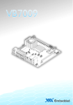
CES-471
COM Express Module
User’s Manual
Edition 1.0
2008/06/16
CES-471 User’s Manual
Copyright
Copyright 2008, all rights reserved. This document is copyrighted and all rights are
reserved. The information in this document is subject to change without prior notice to
make improvements to the products.
This document contains proprietary information and protected by copyright. No part of
this document may be reproduced, copied, or translated in any form or any means
without prior written permission of the manufacturer.
All trademarks and/or registered trademarks contains in this document are property of
their respective owners.
Disclaimer
The company shall not be liable for any incidental or consequential damages resulting
from the performance or use of this product.
The company does not issue a warranty of any kind, express or implied, including
without limitation implied warranties of merchantability or fitness for a particular purpose.
The company has the right to revise the manual or include changes in the specifications
of the product described within it at any time without notice and without obligation to
notify any person of such revision or changes.
Trademark
All trademarks are the property of their respective holders.
Any questions please visit our website at http://www.commell.com.tw
TU
2
UT
CES-471 User’s Manual
Packing List:
Please check the package content before you starting using the board.
Hardware:
CES-471 COM Express module x 1
Attached:
CES-471 heat sink x 1
CD Content:
Drivers & User’s Manual
3
CES-471 User’s Manual
Index
Chapter 1 <Introduction> ............................................................... 6
1.1 <Product Overview> ................................................................. 6
1.2 <Product Specification> ............................................................ 7
1.3 <Mechanical Drawing>............................................................. 9
1.4 <Block Diagram> .................................................................... 10
Chapter 2 <Hardware Setup> .................................................... 12
2.1 <Connector Location>............................................................. 12
2.2 <Connector Reference>........................................................... 13
2.2.1 <Internal Connectors> ......................................................... 13
2.3 <CPU and Memory Setup> ..................................................... 13
2.3.1 <CPU Setup> ..................................................................... 13
2.3.2 <Memory Setup> ................................................................ 14
2.4 <CMOS Setup> ....................................................................... 15
Chapter 3 <System Configuration> ...................................... 16
3.1 <Video Memory Setup> .......................................................... 16
Chapter 4 <BIOS Setup>............................................................... 17
Appendix A <Flash BIOS> ........................................................... 19
A.1 <Flash Tool>........................................................................... 19
A.2 <Flash BIOS Procedure>........................................................ 19
Appendix B <COM Express Pin assignment> .............. 20
Contact Information ......................................................................... 24
4
CES-471 User’s Manual
(This Page is Left for Blank)
5
CES-471 User’s Manual
Chapter 1 <Introduction>
1.1 <Product Overview>
CES-471 is the new generation of the COM express module, with supporting last Intel
Core 2 Duo socket-P processors for 533/800 MHz front side bus, Intel GME965 and
ICH8-M chipset, integrated GMA X3100 graphics, DDR2 SO-DIMM memory, support
High Definition Audio, Serial ATA, PCI Express x16, x1 interface and one Gigabit LAN
Intel Merom dual core Processor
The board supports last Intel Core 2 Duo socket-P processors with 533/800MHz front
side, 2MB L2 cache, to provide more powerful performance than before.
New features for Intel GME965 chipset
The module integrates Intel GME965 and ICH8-M chipset, to provide new generation of
the mobile solution, supports Intel GMA X3100 graphics, DDR2 SO-DIMM 533/667
memory, built-in high speed mass storage interface of serial ATA, High Definition Audio
interface.
All in One multimedia solution
Based on Intel GME965 and ICH8-M chipset, the module provides high performance
onboard graphics, 24-bit dual channel LVDS interface, to meet the very requirement of
the multimedia application.
Flexible Extension Interface
The module support one PCI-Express x16 slot, five PCI-Express x1, it also support four
PCI slots, one Mini PCI.
6
CES-471 User’s Manual
1.2 <Product Specification>
General Specification
Form Factor
CPU
Memory
Chipset
BIOS
Green Function
Watchdog Timer
Real Time Clock
Enhanced IDE
Serial ATA
COM Express Module
Intel® Core 2 Duo Mobile processor
Package type: FCPGA478
L2 Cache: 512KB/1MB/2MB
Front side bus: 533/800 MHz
1 x 200-pin DDR2 SO-DIMM 533/667MHz SDRAM up to 2GB
Unbufferred, none-ECC memory supported only
Intel® GME965 (Northbridge) and ICH8-M (Southbridge)
Phoenix-Award v6.00PG 8Mb SPI flash BIOS
Power saving mode includes doze, standby and suspend
modes. ACPI version 1.0 and APM version 1.2 compliant
System reset programmable watchdog timer.
Intel® ICH8-M built-in RTC
Support UltraDMA100 IDE interface supports up to 2 ATAPI
devices
Intel® ICH8-M integrates support 3 x Serial ATA interfaces
Up to 300MB/s of transfer rate
VGA Display Interface
Chipset
Frame Buffer
Display Type
Intel GME965 GMCH (Graphic Memory Controller Hub)
Up to 384MB shared with system memory
Support CRT, LCD monitor with analog display
Support 24-bit dual channel LVDS interface, HDTV
Ethernet Interface
Controller
Type
Intel 82573L Gigabit Ethernet controller
Triple speed 10/100/1000Base-T
Auto-switching Fast Ethernet
Full duplex, IEEE802.3U compliant
Expansive Interface
PCI-Express
PCI
Audio
Support one x16 PCI-Express slot (compatible with x1 slot)
and five x1 PCI-Express slots
PCI-Express x16 Up to 8GB/s of transfer bandwidth
PCI-Express x1 Up to 5Gb/s of transfer bandwidth
Power supply: +3.3V, +12V
Support four PCI slots, Power supply: +12V, +5VSB
Support ICH8-M HD Audio
Power and Environment
Dimension
Temperature
125(L) x 95 (W) mm
Operating within 0 ~ 60PoPC (32 ~ 140PoPF)
Storage within -20 ~ 85PoPC (-4 ~ 185PoPF)
7
CES-471 User’s Manual
Ordering Code
CES-471
COM Express module for Intel Core 2 Duo Processor
The specifications may be different as the actual production.
For further product information please visit the website at
TUhttp://www.commell.com.twUT
8
CES-471 User’s Manual
‘
‘
‘
‘
‘
‘
‘
1.3 <Mechanical Drawing>
9
CES-471 User’s Manual
1.4 <Block Diagram>
Intel Core 2 Duo Mobile Processors
Intel GMA X3100 Graphics
PCI-Express x16
1 x 200-pin DDR2
LVDS
GME965
SoDIMM 533/667 MHz
up to 2GB
HDTV
UltraDMA100 IDE
3 x Serial ATA ports
8 x USB2.0 ports
HD Audio Interface
Five PCI Express x1
ICH8-M
Four PCI
SPI
BIOS
10
CES-471 User’s Manual
(This Page is Left for Blank)
11
CES-471User’s Manual
Chapter 2 <Hardware Setup>
2.1 <Connector Location>
DDRII SoDIMM
CPU
12
CES-471 User’s Manual
2.2 <Connector Reference>
2.2.1 <Internal Connectors>
Connector
CPU
DDRII
Function
Socket478 for CPU
200 -pin DDR2 SoDIMM slot
Remark
Standard
Standard
2.3 <CPU and Memory Setup>
2.3.1 <CPU Setup>
The module comes with the socket478 for Intel Core 2 Duo Mobile processor, it supports
new generation of Intel Core 2 Duo Mobile processors with 533/800 MHz of front side
bus and 2MB L2 cache. Please follow the instruction to install the CPU properly.
Unlock way
1. Use the flat-type
screw drive to unlock
the CPU socket
Check point
2. Follow the pin direction to install
the processor on the socket
3. Lock the socket
13
CES-471User’s Manual
2.3.2 <Memory Setup>
The module provides one 200-Pin DDRII SoDIMM slot 533/667 memory modules up to
2GB of capacity. Non-ECC, unbuffered memory is supported only.
(1. Insert the DDRII So-DIMM module into the socket at 45 degree)
(2. Press down the module with a click sound)
14
CES-471 User’s Manual
2.4 <CMOS Setup>
The board’s data of CMOS can be setting in BIOS. If the board refuses to boot due to
inappropriate CMOS settings, here is how to proceed to clear (reset) the CMOS to its
default values.
Jumper: JRTC
Type: Onboard 3-pin jumper
JRTC
1-2
2-3
Default setting
Mode
Clear CMOS
Normal Operation
1
3
2.5 <Ethernet Interface>
The Intel 82573L supports triple speed of 10/100/1000Base-T, with IEEE802.3
compliance and Wake-On-LAN supported.
Memory Setup
15
CES-471 User’s Manual
Chapter 3 <System Configuration>
3.1 <Video Memory Setup>
Based on Intel® GME965 chipset with GMA (Graphic Media Accelerator) X3100, the
board supports Intel® DVMT (Dynamic Video Memory Technology) 4.0, which would
allow the video memory be triggered up to 384MB.
To support DVMT, you need to install the Intel® GMA X3100 Driver with supported OS.
BIOS Setup:
On-Chip Video Memory Size: This option combines three items below for setup.
On-Chip Frame Buffer Size:
This item can let you select video memory which been allocated for legacy VGA and
SVGA graphics support and compatibility. The available option is 1MB and 8MB.
DVMT Mode: This item can let you select graphics memory which Fixed or DVMT.
DVMT/FIXED Memory Size:
This item can let you select a maximum size of dynamic amount usage of video memory,
the system would configure the video memory depends on your application, this item is
strongly recommend to be selected as MAX.
16
CES-471 User’s Manual
Chapter 4 <BIOS Setup>
The motherboard uses the Award BIOS for the system configuration. The Award BIOS
in the single board computer is a customized version of the industrial standard BIOS for
IBM PC AT-compatible computers. It supports Intel x86 and compatible CPU
architecture based processors and computers. The BIOS provides critical low-level
support for the system central processing, memory and I/O sub-systems.
The BIOS setup program of the single board computer let the customers modify the
basic configuration setting. The settings are stored in a dedicated battery-backed
memory, NVRAM, retains the information when the power is turned off. If the battery
runs out of the power, then the settings of BIOS will come back to the default setting.
The BIOS section of the manual is subject to change without notice and is provided here
for reference purpose only. The settings and configurations of the BIOS are current at
the time of print, and therefore they may not be exactly the same as that displayed on
your screen.
To activate CMOS Setup program, press <DEL> key immediately after you turn on
the system. The following message “Press DEL to enter SETUP” should appear in the
lower left hand corner of your screen. When you enter the CMOS Setup Utility, the Main
Menu will be displayed as Figure 4-1. You can use arrow keys to select your function,
press <Enter> key to accept the selection and enter the sub-menu.
Figure 4-1 CMOS Setup Utility Main Screen
17
CES-471 User’s Manual
(This Page is Left for Blank)
18
CES-471 User’s Manual
Appendix A <Flash BIOS>
A.1 <Flash Tool>
The board is based on Award BIOS and can be updated easily by the BIOS auto
flash tool. You can download the tool online at the address below:
http://www.phoenix.com/en/home/
http://www.commell.com.tw/Support/Support_SBC.htm
File name of the tool is “awdflash.exe”, it’s the utility that can write the data into the
BIOS flash ship and update the BIOS.
A.2 <Flash BIOS Procedure>
1. Please make a bootable floppy disk.
2. Get the last .bin files you want to update and copy it into the disk.
3. Copy awardflash.exe to the disk.
4. Power on the system and flash the BIOS. (Example: C:/ awardflash XXX.bin)
5. Restart the system.
Any question about the BIOS re-flash please contact your distributors or visit the
web-site at below:
http://www.commell.com.tw/support/support.htm
UT
19
CES-471 User’s Manual
Appendix B <COM Express Pin assignment>
COM A
A1 GND
A26 SATA2RX-
A51 GND
A76 ATX2-
A101 +12V
A2 MDI13-
A27 BATLOW#
A52 N/C
A77 LVDD EN A102 +12V
A3 MDI13+
A28 ATA_ACT#
A53 N/C
A78 ATX3+
A103 +12V
A4 RLINK100#
A29 AC_SYNC
A54 N/C
A79 ATX3-
A104 +12V
A5 RLINK1000# A30 AC_RST#
A55 PCIE_TX5+ A80 GND
A105 +12V
A6 MDI12-
A31 GND
A56 PCIE_TX5- A81 ACLK+
A106 +12V
A7 MDI12+
A32 AC_BITCLK
A57 GND
A107 +12V
A8 RLINK#
A33 AC_SDOUT
A58 PCIE_TX4+ A83 LVDDCLK A108 +12V
A9 MDI11-
A34 N/C
A59 PCIE_TX4- A84 LVDDDAT A109 +12V
A10 MDI11+
A35 -THERMTRIP A60 GND
A11 GND
A36 USBP6-
A61 PCIE_TX3+ A86 -RCIN
A12 MDI10-
A37 USBP+
A62 PCIE_TX3- A87 A20GATE
A13 MDI10+
A38 -USBOC6
A63 N/C
A82 ACLK-
A85 N/C
A88 PCIECLK
A14 GBE_CTREF A39 USBP4-
A64 PCIE_TX2+ A89 -PCIECLK
A15 -SLPS3
A40 USBP4+
A65 PCIE_TX2- A90 GND
A16 SATA0TX+
A41 GND
A66 GND
A91 N/C
A17 SATA0TX-
A42 USBP2-
A67 N/C
A92 N/C
A18 -SLPS4
A43 USBP2+
A68 PCIE_TX+1 A93 N/C
A19 SATA0RX+
A44 -USBOC2
A69 PCIE_TX-1 A94 N/C
A20 SATA0RX-
A45 USBP0-
A70 GND
A95 N/C
A21 GND
A46 USBP0+
A71 ATX0+
A96 GND
A22 SATA2TX+
A47 RTCVCC
A72 ATX0-
A97 +12V
A23 SATA2TX-
A48 N/C
A73 ATX1+
A98 +12V
A24 -SLPS5
A49 N/C
A74 ATX1-
A99 +12V
A25 SATA2RX-
A50 LPC_SERIRQ A75 ATX2+
A100 GND
20
A110 GND
CES-471 User’s Manual
COM B
B1 GND
B26 NC
B51 GND
B76 BTX2-
B101 +12V
B2 ACTLED
B27 WDT
B52 N/C
B77 BTX3+
B102 +12V
B3 -LFRAME
B28 AC SDIN2 B53 N/C
B78 BTX3-
B103 +12V
B4 LAD0
B29 AC SDIN1 B54 N/C
B79 BKL EN
B104 +12V
B5 LAD1
B30 AC SDIN0 B55 PCIE_RX5+ B80 GND
B105 +12V
B6 LAD2
B31 GND
B106 +12V
B7 LAD3
B32 ICHSPKR B57 N/C
B8 -LDRQ0
B33 I2C_CK
B9 -LDRQ1
B34 I2C_DAT B59 PCIE_RX4- B84 5VDU
B56 PCIE_RX5- B81 BCLK+
B82 BCLK-
B58 PCIE_RX4+ B83 BKL CRTL B108 +12V
B10 LPC33CLK B35 THERM# B60 GND
B85 5VDU
B11 GND
B36 USBP7-
B61 PCIE_RX3+ B86 5VDU
B12 -ICHBTN
B37 USBP7+
B62 PCIE_RX3- B87 5VDU
B13 SMBCLK
B38 -USBOC4 B63 N/C
B64 PCIE_RX2+ B89 CRT R
B15 GPI11
B65 PCIE_RX2- B90 GND
B16 SATA1TX+ B41 GND
B66 -PCIEWK
B91 CRT G
B17 SATA1TX- B42 USBP3-
B67 -LPCME
B92 CRT B
B18 -SUSTAT
B68 PCIE RX1+ B93 CRT HS
B43 USBP3+
B109 +12V
B110 GND
B88 N/C
B14 SMBDATA B39 USBP5B40 USBP5+
B107 +12V
B19 SATA1RX+ B44 -USBOC0 B69 PCIE RX1- B94 CRT VS
B20 SATA1RX- B45 USBP1-
B70 GND
B95 CRTDCLK
B21 GND
B46 USBP1+
B71 BTX0+
B96 CRTDDAT
B22 NC
B47 N/C
B72 BTX0-
B97 TVA PB
B23 NC-
B48 N/C
B73 BTX1+
B98 TVB Y
B24 PWR_GD
B49 -SYSRST B74 BTX1-
B99 TVC PR
B25 NC
B50 -CBRST
B100 GND
B75 BTX2+
21
CES-471 User’s Manual
COM C
C1 GND
C26 AD4
C51 GND
C76 GND
C2 PDD7
C27 AD6
C52 PEG RX0+ C77 N/C
C3 PDD6
C28 AD8
C53 PEG RX0- C78 PEG RX8+ C103 GND
C4 PDD3
C29 AD10
C54 N/C
C5 PDD15
C30 AD12
C55 PEG RX1+ C80 GND
C6 PDD8
C31 GND
C56 PEG RX1- C81 PEG RX9+ C106 +12V
C7 PDD9
C32 AD14
C57 N/C
C8 PDD2
C33 -CBE1
C58 PEG RX2+ C83 N/C
C108 +12V
C9 PDD13
C34 -PERR
C59 PEG RX2- C84 GND
C109 +12V
C10 PDD1
C35 -PLOCK C60 GND
C11 GND
C36 -DEVSEL C61 PEG RX3+ C86 PEG RX10-
C12 PDD14
C37 -IRDY
C79 PEG RX8-
C82 PEG RX9-
C102 PEG RXN16
C104 +12V
C105 +12V
C107 +12V
C85 PEG RX10+ C110 GND
C62 PEG RX3- C87 GND
C13 PIORDY C38 -CBE2
C63 N/C
C88 PEG RX11+
C14 -PDIOR C39 AD17
C64 N/C
C89 PEG RX11-
C15 -PME
C40 AD19
C65 PEG RX4+ C90 GND
C16 -GNT2
C41 GND
C66 PEG RX4- C91 PEG RX12+
C17 -REQ2
C42 AD21
C67 N/C
C18 -GNT1
C43 AD23
C68 PEG RX5+ C93 GND
C19 -REQ1
C44 -CBE3
C69 PEG RX5- C94 PEG RX13+
C20 -GNT0
C45 AD25
C70 GND
C21 GND
C46 AD27
C71 PEG RX6+ C96 GND
C22 -REQ0
C47 AD29
C72 PEG RX6- C97 N/C
C92 PEG RX12-
C95 PEG RX13-
C23 -PCIRST C48 AD31
C73 SDVODAT C98 PEG RX14+
C24 AD0
C49 -PIRQA
C74 PEG RX7+ C99 PEG RX14-
C25 AD2
C50 -PIRQB
C75 PEG RX7- C100 GND
22
C101 PEG RXP15
CES-471 User’s Manual
COM D
D1 GND
D26 -CBE0
D51 GND
D76 GND
D2 PDD5
D27 AD9
D52 PEG TX0+ D77 P66DET
D3 PDD10
D28 AD11
D53 PEG TX0- D78 PEG TX8+ D103 GND
D4 PDD11
D29 AD13
D54 CFG9
D5 PDD12
D30 AD15
D55 PEG TX1+ D80 GND
D6 PDD4
D31 GND
D56 PEG TX1- D81 PEG TX9+ D106 +12V
D7 PDD0
D32 PAR
D57 N/C
D79 PEG TX8-
D82 PEG TX9-
D101 PEG TX15+
D102 PEG TX15-
D104 +12V
D105 +12V
D107 +12V
D8 PDDREQ D33 -SERR
D58 PEG TX2+ D83 N/C
D108 +12V
D9 -PDIOW
D59 PEG TX2- D84 GND
D109 +12V
D34 -STOP
D10 -PDDACK D35 -TRDY
D60 GND
D85 PEG TX10+ D110 GND
D11 GND
D36 -FRAME D61 PEG TX3+ D86 PEG TX10-
D12 IDEIRQ
D37 AD16
D62 PEG TX3- D87 GND
D13 PAD0
D38 AD18
D63 N/C
D88 PEG TX11+
D14 PAD1
D39 AD20
D64 N/C
D89 PEG TX11-
D15 PAD2
D40 AD22
D65 PEG TX4+ D90 GND
D16 -PCS1
D41 GND
D66 PEG TX4- D91 PEG TX12+
D17 -PCS3
D42 AD24
D67 GND
D18 IDERST
D43 AD26
D68 PEG TX5+ D93 GND
D19 -GNT3
D44 AD28
D69 PEG TX5- D94 PEG TX13+
D20 -REQ3
D45 AD30
D70 GND
D21 GND
D46 -PIRQC
D71 PEG TX6+ D96 GND
D22 AD1
D47 -PIRQD
D72 PEG TX6- D97 N/C
D23 AD3
D48 N/C
D73 SDVOCLK D98 PEG TX14+
D24 AD5
D49 N/C
D74 PEG TX7+ D99 PEG TX14-
D25 AD7
D50 PCISCLK D75 PEG TX7- D100 GND
D92 PEG TX12-
D95 PEG TX13-
23
CES-471 User’s Manual
Contact Information
Any advice or comment about our products and service, or
anything we can help you please don’t hesitate to contact with us.
We will do our best to support you for your products, projects a
business.
Taiwan Commate Computer Inc.
Address
8F, No. 94, Sec. 1, Shin Tai Wu Rd., Shi Chih
Taipei Hsien, Taiwan
TEL
+886-2-26963909
FAX
+886-2-26963911
http://www.commell.com.tw
Website
TU
UT
[email protected] (General Information)
E-Mail
TU
UT
[email protected] (Technical Support)
TU
UT
Commell is our trademark of industrial PC division
24