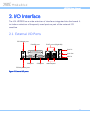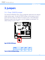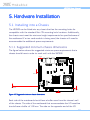
1
USER MANUAL VB7009 Mini-ITX embedded board 1.15-07012013-172200 Copyright Copyright © 2013 VIA Technologies Incorporated. All rights reserved. No part of this document may be reproduced, transmitted, transcribed, stored in a retrieval system, or translated into any language, in any form or by any means, electronic, mechanical, magnetic, optical, chemical, manual or otherwise without the prior written permission of VIA Technologies, Incorporated. Trademarks All trademarks are the property of their respective holders. Disclaimer No license is granted, implied or otherwise, under any patent or patent rights of VIA Technologies. VIA Technologies makes no warranties, implied or otherwise, in regard to this document and to the products described in this document. The information provided in this document is believed to be accurate and reliable as of the publication date of this document. However, VIA Technologies assumes no responsibility for the use or misuse of the information (including use or connection of extra device/equipment/add-on card) in this document and for any patent infringements that may arise from the use of this document. The information and product specifications within this document are subject to change at any time, without notice and without obligation to notify any person of such change. VIA Technologies, Inc. reserves the right the make changes to the products described in this manual at any time without prior notice. Regulatory Compliance FCCFCC-A Radio Frequency Interference Statement This equipment has been tested and found to comply with the limits for a class A digital device, pursuant to part 15 of the FCC rules. These limits are designed to provide reasonable protection against harmful interference when the equipment is operated in a commercial environment. This equipment generates, uses, and can radiate radio frequency energy and, if not installed and used in accordance with the instruction manual, may cause harmful interference to radio communications. Operation of this equipment in a residential area is likely to cause harmful interference, in which case the user will be required to correct the interference at his personal expense. Notice 1 The changes or modifications not expressly approved by the party responsible for compliance could void the user's authority to operate the equipment. Notice 2 Shielded interface cables and A.C. power cord, if any, must be used in order to comply with the emission limits. Notice 3 The product described in this document is designed for general use, VIA Technologies assumes no responsibility for the conflicts or damages arising from incompatibility of the product. Check compatibility issue with your local sales representatives before placing an order. Tested To Comply With FCC Standards FOR HOME OR OFFICE USE Battery Recycling and Disposal Only use the appropriate battery specified for this product. Do not re-use, recharge, or reheat an old battery. Do not attempt to force open the battery. Do not discard used batteries with regular trash. Discard used batteries according to local regulations. Safety Precautions Always read the safety instructions carefully. Keep this User's Manual for future reference. All cautions and warnings on the equipment should be noted. Keep this equipment away from humidity. Lay this equipment on a reliable flat surface before setting it up. Make sure the voltage of the power source and adjust properly 110/220V before connecting the equipment to the power inlet. Place the power cord in such a way that people cannot step on it. Always unplug the power cord before inserting any add-on card or module. If any of the following situations arises, get the equipment checked by authorized service personnel: The power cord or plug is damaged. Liquid has penetrated into the equipment. The equipment has been exposed to moisture. The equipment has not worked well or you cannot get it work according to User's Manual. The equipment has dropped and damaged. The equipment has obvious sign of breakage. Do not leave this equipment in an environment unconditioned or in a storage temperature above 60°C (140°F). The equipment may be damaged. Do not leave this equipment in direct sunlight. Never pour any liquid into the opening. Liquid can cause damage or electrical shock. Do not place anything over the power cord. Do not cover the ventilation holes. The openings on the enclosure protect the equipment from overheating VB7009 User Manual Box Contents and Ordering Information VB7009VB7009-16 1 x VB7009 embedded board (with C7®-D 1.6 GHz NanoBGA2 processor) 1 x I/O bracket 1 x SATA cable VB7009VB7009-10E 1 x VB7009 embedded board (with C7® 1.0 GHz NanoBGA2 processor) 1 x I/O bracket 1 x SATA cable VB7009VB7009-12XC 1 x VB7009 embedded board (with NanoX2 1.2 GHz NanoBGA2 processor) 1 x I/O bracket 1 x SATA cable iv VB7009 User Manual Table of Contents 1. Product Overview ................................................................ ................................................................................................ ................................................................ 1 1.1. Key Features and Benefits........................................................................... 1 1.1.1. VIA C7®-D / C7® / Nano X2 NanoBGA2 Processor ........................ 1 1.1.2. VIA VX900 Chipset................................................................................. 2 1.1.3. Modular Expansion Options................................................................. 2 1.2. Product Specifications................................................................................. 3 1.3. Layout Diagram ............................................................................................. 6 1.4. Product Dimensions..................................................................................... 7 1.5. Height Distribution....................................................................................... 8 2. I/O Interface................................ Interface................................................................ ................................................................................................ .......................................................................... .......................................... 9 2.1. External I/O Ports ......................................................................................... 9 2.1.1. PS/2 Port.................................................................................................. 10 2.1.2. VGA Port................................................................................................. 10 2.1.3. COM Port................................................................................................ 12 2.1.4. Parallel Port............................................................................................ 13 2.1.5. RJ45 LAN port: Gigabit Ethernet ....................................................... 14 2.1.6. USB 2.0 Port ........................................................................................... 15 2.1.7. Audio Ports............................................................................................. 16 2.2. Onboard Connectors ................................................................................ 17 2.2.1. ATX Power Connector......................................................................... 17 2.2.2. CMOS Battery Slot................................................................................ 18 2.2.3. Front Panel Pin Header ........................................................................ 19 2.2.4. Front Audio Pin Header....................................................................... 20 2.2.5. SMBus Pin Header................................................................................. 21 2.2.6. CPU and System Fan Connectors ...................................................... 22 2.2.7. SATA Connectors ................................................................................. 23 2.2.8. USB 2.0 Pin Headers............................................................................. 24 2.2.9. COM Pin Headers ................................................................................. 25 2.2.10. PS/2 Keyboard and Mouse Pin Header ............................................ 26 v VB7009 User Manual 2.2.11. 2.2.12. 2.2.13. 2.2.14. 2.2.15. 2.2.16. 2.2.17. LVDS Connector.................................................................................... 27 Inverter Connector................................................................................ 29 SPDIF Connector ................................................................................... 30 SPI Pin Header ....................................................................................... 31 LPC Pin Header ...................................................................................... 32 Digital I/O Pin Header.......................................................................... 33 Temperature Sensor Pin Header........................................................ 34 3. Jumpers ................................................................ ................................................................................................ ............................................................................... ............................................... 35 3.1. Clear CMOS Jumper.................................................................................. 35 3.2. COM Voltage Select Jumpers................................................................. 37 3.2.1. COM2 Voltage Select Jumper........................................................... 37 3.2.2. COM3 and COM4 Voltage Select Jumper ..................................... 38 3.2.3. COM5 and COM6 Voltage Select Jumper ..................................... 39 3.3. SATA DOM Voltage Select Jumper ...................................................... 40 3.4. Panel Power Select Jumper ..................................................................... 41 3.5. Backlight Power Select Jumper............................................................... 42 4. Expansion Slots ................................................................ ................................................................................................ .................................................................. .................................. 43 4.1. DDR3 Memory Slots .................................................................................. 43 4.1.1. Installing a Memory Module .............................................................. 44 4.1.2. Removing a Memory Module............................................................. 46 4.1.3. PCI Slot.................................................................................................... 47 5. Hardware Installation ................................................................ ........................................................................................ ........................................................ 49 5.1. Installing into a Chassis............................................................................. 49 5.1.1. Suggested minimum chassis dimensions ......................................... 49 5.1.2. Suggested minimum chassis height................................................... 50 5.1.3. Suggested keepout areas .................................................................... 51 6. BIOS Setup Utility ................................................................ .............................................................................................. .............................................................. 53 6.1. Entering the BIOS Setup Utility............................................................... 53 6.2. Control Keys................................................................................................ 53 vi VB7009 User Manual 6.3. Navigating the BIOS Menus ..................................................................... 54 6.4. Getting Help................................................................................................ 54 6.5. Main Menu ................................................................................................... 55 6.5.1. Standard CMOS Features .................................................................... 55 6.5.2. Advanced BIOS Features..................................................................... 55 6.5.3. Advanced Chipset Features ................................................................ 55 6.5.4. Integrated Peripherals.......................................................................... 55 6.5.5. Power Management Setup.................................................................. 56 6.5.6. PnP/PCI Configurations......................................................................... 56 6.5.7. PC Health Status.................................................................................... 56 6.5.8. Frequency/Voltage Control ................................................................ 56 6.5.9. Load Optimized Defaults.................................................................... 56 6.5.10. Set Supervisor Password ..................................................................... 56 6.5.11. Set User Password ................................................................................ 56 6.5.12. Save & Exit Setup .................................................................................. 56 6.5.13. Exit Without Saving............................................................................... 56 6.6. Standard CMOS Features ......................................................................... 57 6.6.1. Date.......................................................................................................... 57 6.6.2. Time ......................................................................................................... 57 6.6.3. Video ....................................................................................................... 57 6.6.4. Halt On ................................................................................................... 57 6.7. IDE Channels ............................................................................................... 58 6.8. Advanced BIOS Features .......................................................................... 60 6.8.1. Quick Power On Self-Test .................................................................. 60 6.8.2. First/Second/Third Boot Device ......................................................... 60 6.8.3. Boot Other Device................................................................................ 61 6.8.4. Boot Up NumLock Status .................................................................... 61 6.8.5. Security Option ..................................................................................... 61 6.8.6. Full Screen Logo Show........................................................................ 61 6.8.7. Summary Screen Show ........................................................................ 61 6.9. CPU Feature ................................................................................................. 62 6.9.1. Thermal Management .......................................................................... 62 6.9.2. PMON support ...................................................................................... 62 vii VB7009 User Manual 6.10. Hard Disk Boot Priority.............................................................................. 63 6.11. Advanced Chipset Features ..................................................................... 64 6.11.1. LCD Clock Source Control ................................................................. 64 6.11.2. LCD Backlight Control ......................................................................... 64 6.12. PCIE Bus Control ........................................................................................ 65 6.12.1. PCIE Root Port........................................................................................ 65 6.12.2. PCIE Target Link Speed........................................................................ 65 6.12.3. PCIE PE0 Control................................................................................... 65 6.12.4. PCIE Hot-Reset Enable......................................................................... 65 6.12.5. PCIE Root-Port-Reset Enable.............................................................. 65 6.12.6. Maximum Payload Size........................................................................ 65 6.12.7. PCIE ASPM Function ............................................................................. 66 6.13. UMA & P2P Bridge Control...................................................................... 67 6.13.1. UMA Enable ........................................................................................... 67 6.13.2. VGA Share Memory Size ..................................................................... 67 6.13.3. CPU Direct Access FB .......................................................................... 67 6.13.4. Select Display Device.......................................................................... 67 6.13.5. Select Display Device 1 ...................................................................... 67 6.13.6. Select Display Device 2 ...................................................................... 68 6.13.7. Panel Type .............................................................................................. 68 6.13.8. Engine Clock Control........................................................................... 68 6.14. CPU & PCI Bus Control ............................................................................. 69 6.14.1. PCI Master 0 WS Write ........................................................................ 69 6.14.2. PCI Delay Transaction .......................................................................... 69 6.14.3. SB P2P Bridge......................................................................................... 69 6.15. Integrated Peripherals ............................................................................... 70 6.16. VIA OnChip IDE Device............................................................................ 71 6.16.1. OnChip SATA ........................................................................................ 71 6.17. VIA OnChip PCI Device ............................................................................ 72 6.17.1. Onboard PCIE LAN............................................................................... 72 6.17.2. Hide D1F1............................................................................................... 72 6.17.3. OnChip HDAC Device......................................................................... 72 6.17.4. Clear HDA Wake Enable bit .............................................................. 72 viii VB7009 User Manual 6.17.5. NB HD Audio Codec 1........................................................................ 72 6.18. SuperIO Device .......................................................................................... 73 6.18.1. Onboard Serial Ports 1 ~ 4 ................................................................ 73 6.18.2. Onboard Parallel Port ......................................................................... 73 6.18.3. Parallel Port Mode................................................................................ 73 6.18.4. ECP Mode Use DMA ............................................................................ 74 6.19. USB Device Setting .................................................................................... 75 6.19.1. USB 1.0 Controller................................................................................ 75 6.19.2. USB 2.0 Controller................................................................................ 75 6.19.3. USB Operation Mode........................................................................... 75 6.19.4. USB Keyboard Function ....................................................................... 75 6.19.5. USB Mouse Function............................................................................. 76 6.19.6. USB Storage Function........................................................................... 76 6.20. Power Management Setup ....................................................................... 77 6.20.1. EuP/ErP Lot6 ........................................................................................... 77 6.20.2. ACPI Suspend Type .............................................................................. 77 6.20.3. Soft-Off by PWRBTN............................................................................ 78 6.20.4. Run VGABIOS if S3 Resume ............................................................... 78 6.20.5. AC Loss Auto Restart ........................................................................... 78 6.20.6. HPET Support ........................................................................................ 78 6.20.7. WDRT Support ...................................................................................... 78 6.20.8. WDRT Run/Stop..................................................................................... 78 6.20.9. WDRT Count .......................................................................................... 79 6.21. Wakeup Event Detect................................................................................ 80 6.21.1. PS2KB Wakeup Select.......................................................................... 80 6.21.2. PS2KB Wakeup Key Select.................................................................. 80 6.21.3. PS2MS Wakeup Key Select................................................................. 80 6.21.4. PS2 Keyboard Power ON.................................................................... 81 6.21.5. PS2 Mouse Power ON ......................................................................... 81 6.21.6. RTC Alarm Resume............................................................................... 81 6.21.7. Date (of Month)..................................................................................... 81 6.21.8. Resume Time (hh:mm:ss) .................................................................... 81 6.22. PnP/PCI Configurations.............................................................................. 82 ix VB7009 User Manual 6.22.1. Init Display First ..................................................................................... 82 6.22.2. Resources Controlled By..................................................................... 82 6.23 PC Health Status ................................................................................................ 83 6.24 Frequency/Voltage Control ..................................................................... 84 6.24.1 DRAM Clock........................................................................................... 84 6.24.2 Spread Spectrum................................................................................... 84 6.25 Load Optimized Defaults ......................................................................... 85 6.26 Set Supervisor/User Password................................................................. 86 6.27 Save & Exit Setup ....................................................................................... 88 6.28 Exit Without Saving.................................................................................... 89 7 Driver Installation................................ Installation................................................................ ............................................................................................... ............................................................... 91 7.1 Microsoft Driver Support ............................................................................... 91 7.2 Linux Driver Support....................................................................................... 91 Appendix A. Power Consumption Report................................ Report............................................................... ............................................................... 93 A.1. VB7009-16............................................................................................................ 93 A.1.1. System Idle – Windows 7 32-bit ............................................................ 93 A.1.2. S3 Status – Windows 7 Sleep.................................................................. 94 A.1.3. MP3 Playback – Windows Media Player10........................................... 94 A.1.4. DVD Playback – PowerDVD 8.0.............................................................. 94 A.1.5. Graphics – Run 3DMarks’06...................................................................... 94 A.1.6. Functional Test – Run Passmark BurnIn test 6.0 ................................... 95 A.1.7. Network Access <Single LAN> – Gigabit Ethernet File Transmitting .................................................................................................................................... 95 A.1.8. Network Access <Dual LAN> – Gigabit Ethernet File Transmitting. 96 A.2. VB7009-10E ......................................................................................................... 97 A.2.1. System Idle – Windows 7 32-bit ............................................................ 97 A.2.2. S3 Status – Windows 7 Sleep.................................................................. 97 A.2.3. MP3 Playback – Windows Media Player10........................................... 98 A.2.4. DVD Playback – PowerDVD 8.0.............................................................. 98 A.2.5. Graphics – Run 3DMarks’06...................................................................... 98 A.2.6. Functional Test – Run Passmark BurnIn test 6.0 ................................... 99 x VB7009 User Manual A.2.7. Network Access <Single LAN> – Gigabit Ethernet File Transmitting .................................................................................................................................... 99 A.2.8. Network Access <Dual LAN> – Gigabit Ethernet File Transmitting. 99 A.3. VB7009-12XC ....................................................................................................100 A.3.1. System Idle – Windows 7 32-bit ..........................................................100 A.3.2. S3 Status – Windows 7 Sleep................................................................100 A.3.3. MP3 Playback – Windows Media Player10.........................................101 A.3.4. DVD Playback – Windows Media Player10........................................101 A.3.5. Graphics – Run 3DMarks’06....................................................................101 A.3.6. Functional Test – Run Passmark BurnIn test 6.0 .................................102 A.3.7. Network Access <Single LAN> – Gigabit Ethernet File Transmitting ..................................................................................................................................102 A.3.8. Network Access <Dual LAN> – Gigabit Ethernet File Transmitting ..................................................................................................................................102 A.3.9. S5 Status – Windows 7 Shut down ...........................................................103 Appendix B. Mating Connector Vendor Lists................................ Lists........................................................ ........................................................ 105 xi VB7009 User Manual Lists of Figures Figure 1: Layout diagram of the VB7009 mainboard (top view) ............................ 6 Figure 2: Mounting holes and dimensions of the VB7009 mainboard .................. 7 Figure 3: External I/O port dimensions of the VB7009 mainboard........................ 7 Figure 4: Height distribution of the VB7009 mainboard........................................... 8 Figure 5: External I/O ports............................................................................................. 9 Figure 6: PS/2 port pinout diagram ............................................................................. 10 Figure 7: VGA port pinout diagram............................................................................. 10 Figure 8: COM port pinout diagram............................................................................ 12 Figure 9: Parallel port pinout diagram ....................................................................... 13 Figure 10: Gigabit Ethernet port pinout diagram ..................................................... 14 Figure 11: USB port pinout diagram............................................................................ 15 Figure 12: Audio jack receptacle stack....................................................................... 16 Figure 13: ATX power connector ................................................................................ 17 Figure 14: CMOS battery slot....................................................................................... 18 Figure 15: Front panel pin header ............................................................................... 19 Figure 16: Front audio pin header ............................................................................... 20 Figure 17: SMBus pin header pinout ........................................................................... 21 Figure 18: Fan connectors.............................................................................................. 22 Figure 19: SATA connectors ......................................................................................... 23 Figure 20: USB 2.0 pin headers .................................................................................... 24 Figure 21: COM pin header........................................................................................... 25 Figure 22: PS/2 keyboard and mouse pin header .................................................... 26 Figure 23: LVDS connector ........................................................................................... 27 Figure 24: Inverter connector ....................................................................................... 29 Figure 25: SPDIF connector ........................................................................................... 30 Figure 26: SPI pin header ............................................................................................... 31 Figure 27: LPC pin header.............................................................................................. 32 Figure 28: Digital I/O pin header ................................................................................. 33 Figure 29: Temperature sensor pin header................................................................ 34 Figure 30: CLEAR CMOS jumper ................................................................................. 35 Figure 31: COM2 voltage select jumper.................................................................... 37 xii VB7009 User Manual Figure 32: Voltage select jumpers for COM3 and COM4 ..................................... 38 Figure 33: Voltage select jumpers for COM5 and COM6 ..................................... 39 Figure 34: SATA DOM voltage select jumper.......................................................... 40 Figure 35: LVDS power select jumper........................................................................ 41 Figure 36: Backlight power select jumper................................................................. 42 Figure 37: DDR3 memory slots .................................................................................... 43 Figure 38: Unlocking the memory DIMM slot........................................................... 44 Figure 39: Inserting the memory module................................................................... 44 Figure 40: Locking the memory module .................................................................... 45 Figure 41: Removing the memory module ................................................................ 46 Figure 42: PCI slot ........................................................................................................... 47 Figure 43: Suggested minimum chassis dimensions ................................................ 49 Figure 44: Suggested minimum internal chassis ceiling height............................. 50 Figure 45: Suggested keepout areas ........................................................................... 51 Figure 46: Illustration of the Main menu screen....................................................... 55 xiii VB7009 User Manual Lists of Tables Table 1: PS/2 port pinout .............................................................................................. 10 Table 2: VGA port pinout ............................................................................................. 11 Table 3: COM port pinout ............................................................................................ 12 Table 4: Parallel port pinout ........................................................................................ 13 Table 5: Gigabit Ethernet port pinout ........................................................................ 14 Table 6: Gigabit Ethernet LED color definition ........................................................ 14 Table 7: USB 2.0 port pinout........................................................................................ 15 Table 8: Audio jack receptacle pinout....................................................................... 16 Table 9: ATX power connector pinout...................................................................... 17 Table 10: CMOS battery slot pinout .......................................................................... 18 Table 11: Front panel pin header pinout................................................................... 19 Table 12: Front audio pin header pinout................................................................... 20 Table 13: SMBus pin header ......................................................................................... 21 Table 14: Fan connector pinouts ................................................................................. 22 Table 15: SATA connector pinouts............................................................................. 23 Table 16: USB 2.0 pin header pinouts........................................................................ 24 Table 17: COM pin header pinout.............................................................................. 25 Table 18: PS/2 keyboard and mouse pin header pinout........................................ 26 Table 19: LVDS connector pinout............................................................................... 28 Table 20: Inverter connector pinout........................................................................... 29 Table 21: SPDIF connector pinout .............................................................................. 30 Table 22: SPI pin header pinout .................................................................................. 31 Table 23: LPC pin header pinout................................................................................. 32 Table 24: Digital I/O pin header pinout .................................................................... 33 Table 25: Temperature sensor pin header pinout ................................................... 34 Table 26: CLEAR CMOS jumper settings................................................................... 35 Table 27: COM2 voltage select jumper settings ..................................................... 37 Table 28: Jumper settings for COM3 and COM4 .................................................... 38 Table 29: Jumper settings for COM5 and COM6 .................................................... 39 Table 30: SATA DOM voltage select jumper settings ........................................... 40 Table 31: LVDS power select jumper settings ......................................................... 41 xiv VB7009 User Manual Table 32: Backlight power select jumper settings .................................................. 42 Table 33: VB7009 mating connector vendor lists .................................................105 xv VB7009 User Manual 1. Product Overview The VIA VB7009 Mini-ITX mainboard is an entry-level native x86 mainboard designed mainly for embedded and thin client applications. It can also be used for various domain applications such as desktop PC, industrial PC, etc. The mainboard is based on the VIA VX900 Unified Digital Media IGP chipset that features the VIA Chrome™ 9 HC with 2D/3D graphics and video accelerators for rich digital media performance. The VIA VB7009 includes a secure and power efficient VIA C7®-D / C7® / Nano X2 NanoBGA2 processor. The VIA C7®-D / C7® / Nano X2 NanoBGA2 processor includes the VIA Padlock Security Engine, VIA StepAhead™ Technology Suite, VIA PowerSaver™, and VIA CoolStream™ technology. The VIA VB7009 has one 1066 MHz DDR3 DIMM slot that support up to 4 GB memory size. The VIA VB7009 provides support for high fidelity audio with its included VIA VT1708S High Definition Audio codec. In addition it supports two SATA 3Gb/s storage devices. The VIA VB7009 is compatible with a full range of Mini-ITX chassis as well as FlexATX and MicroATX enclosures and power supplies. The VIA VB7009 is fully compatible with Microsoft® and Linux operating systems. 1.1. Key Features and Benefits 1.1.1. VIA C7®-D / C7® / Nano X2 NanoBGA2 Processor The VIA C7®-D / C7® / Nano X2 NanoBGA2 is an x86 processor packed into an ultra compact NanoBGA2 package (measuring 21mm x 21mm). It delivers an energy-efficient yet powerful performance, with cool and quiet operation that makes it ideal for embedded system applications. The VIA C7®-D / C7® is a single core 32-bit processor based on 90 nanometer process technology, and it is the world’s first Carbon Free processor. 1 VB7009 User Manual The VIA Nano X2 is a 64-bit dual core processor that can deliver an improved multitasking ability without consuming more power. It is based on the latest 40 nanometer process technology. 1.1.2. VIA VX900 Chipset The VIA VX900 Unified Digital Media Chipset is designed to enable high quality digital video streaming and DVD playback in a new generation of fanless, small form factor PCs and IA devices. The VIA VX900 features VIA Chrome™ 9 HC3 with 2D/3D graphics and video acceleration, DDR3 1066/800 support, motion compensation and dual display support to ensure a rich overall entertainment experience. 1.1.3. Modular Expansion Options The VIA VB7009 ensures long-term usability with its support for industry standard expansion options. Its support for legacy PCI expansion cards helps to smooth and reduce the costs of transitioning to newer expansion technologies. The VIA VB7009 enables companies to slowly roll out upgrades as necessary instead of having to replace everything all at once. This ensures that companies using the VB7009 obtain the maximum benefits from its past investments in PCI expansion cards. 2 VB7009 User Manual 1.2. Product Specifications Processor ® 1 VIA C7 -D 1.6 GHz NanoBGA2 (for VB7009-16 SKU ) Supports 800MHz Front Side Bus 21 x 21 mm FCBGA ® 2 VIA C7 1.0 GHz NanoBGA2 (for VB7009-10E SKU ) Supports 400MHz Front Side Bus 21 x 21 mm FCBGA 1 VIA Nano X2 1.2 GHz NanoBGA2 (for VB7009-12XC SKU ) Supports 800MHz Front Side Bus 21 x 21 mm FCBGA Chipset VIA VX900 Unified Digital Media IGP chipset 31 mm x 31 mm FCBGA System Memory 1 x DIMM slot supporting DDR3 1066 MHz Supports up to 4 GB memory size Graphics Integrated VIA Chrome™ 9 HC3 3D/2D AGP graphics MPEG2, WMV9/VC1, H.264 Full HD video decoder DirectX 9 support Onboard Peripherals Serial ATA 2 SATA connectors Supports up to 3 Gb/s Onboard LAN VIA VT6130 PCIe Gigabit Ethernet controller Onboard LVDS VIA VT1636 LVDS transmitter Onboard Audio VIA VT1708S High Definition Audio Codec Onboard Super II/ /O Fintek F81865F-I Super I/O controller Supports up to four COM ports 3 VB7009 User Manual Onboard I/O Connectors 2 x USB 2.0 pin headers for 4 USB ports 2 x SATA 2.0 HDD connectors 1 x Front audio pin header for Line-Out and MIC-In 1 x Front panel pin header 1 x PS/2 Keyboard and Mouse pin header 1 x Digital I/O (GPI x 4 + GPO x 4) 1 x CPU fan connector 1 x System fan connector 3 x COM pin headers by F81865-I, with 5V/12V select 5 x COM pin headers by F81865-I, with 5V/12V select (available only for VB7009-12XC) 1 x PCI slot 1 x Dual-channel LVDS connector (18/24 bit) 1 x LVDS inverter pin header 1 x LPC pin header 1 x SPDIF connector 1 x SPI pin header 1 x SMBus pin header 1 x Temperature Sensor pin header 1 x Clear CMOS jumper 1 x COM2 voltage selector jumper 1 x COM3 and COM4 voltage selector jumper 1 x COM5 and COM6 voltage selector jumper (available only for VB7009-12XC) 1 x SATA DOM voltage select jumper 1 x LVDS panel power selector jumper (5V/3.3V) 1 x LVDS inverter power selector jumper (5V/12V) 1 x Buzzer 1 x ATX (20-pin) power connector Back Panel I/O 1 x VGA port 1 x COM port 1 x Parallel port 2 x RJ45 (GigaLAN) port 4 x USB 2.0 ports 1 x PS/2 Keyboard port 1 x PS/2 Mouse port 3 x Audio jacks: Line-In, Line-Out, MIC-In (Vertical, Smart 5.1 support) 4 VB7009 User Manual BIOS Award BIOS 8 Mbit SPI flash memory Supported Operating System Windows 7 Windows Embedded Standard 7 Windows Embedded POSReady 7 Windows Embedded Standard Windows XP Windows CE Linux System Monitoring Monitoring & Management Wake-on-LAN Wake-on-Keyboard Wake-on-Mouse RTC Timer to Power On AC power failure recovery Operating Conditions Operating Temperature 0°C up to 60°C Operating Humidity 0% ~ 95% (relative humidity; non-condensing) Form Factor Mini-ITX 17 cm x 17 cm Compliance CE FCC RoHS Notes: 1. The VB7009-16 and VB7009-12XC SKUs uses heatsink with fan. 2. The VB7009-10E SKU uses heatsink only. 5 VB7009 User Manual 1.3. Layout Diagram Figure 1: Layout diagram of the VB7009 mainboard (top view) view) Notes: The additional COM pin headers labeled as “COM5” and “COM6” are available only in VB7009-12XC SKU. 6 VB7009 User Manual 1.4. Product Dimensions 170.00 mm 7.92 mm 10.16 mm 33.02 mm 39.37 mm 170.00 mm 4.97 mm 6.17 mm 6.35 mm Figure 2: Mounting holes and dimensions of the VB7009 mainboard 31.50 mm 25.55 mm 21.75 mm 19.00 mm 6.25 mm 6.50 mm 6.50 mm 143.61 mm 121.86 mm 100.21 mm 73.99 mm 55.99 mm 37.98 mm 0.00 11.90 mm 0.00 Figure 3: External I/O port dimensions of the VB7009 mainboard 7 VB7009 User Manual 1.5. Height Distribution Height: 38.50 mm Height: 32.00 mm Height: 33.00 mm Height: 35.00 mm Height: 34.60 mm Figure 4: Height distribution of the VB7009 mainboard 8 VB7009 User Manual 2. I/O Interface The VIA VB7009 has a wide selection of interfaces integrated into the board. It includes a selection of frequently used ports as part of the external I/O coastline. 2.1. External I/O Ports PS2 Mouse port Parallel port RJ-45 ports (GigaLAN) Line-In Line-Out MIC-In VGA port COM port USB 2.0 ports PS2 Keyboard port Figure 5: External I/O ports 9 VB7009 User Manual 2.1.1. PS/2 Port The mainboard has two integrated PS/2 ports for keyboard and mouse. Each port is using the 6-pin Mini-DIN connector. The color purple is use for a PS/2 keyboard while the color green is use for a PS/2 mouse. The pinout of the PS/2 port are shown below. Pin Signal 1 Data 2 NC 3 GND 4 +5V 5 Clock 6 NC 5 6 4 3 2 1 Table 1: PS/2 port pinout Figure 6: PS/2 port pinout diagram 2.1.2. VGA Port The integrated 15-pin VGA port uses a female DE-15 connector. The VGA port is for connecting to analog displays. The pinout of the VGA port is shown below. Figure 7: VGA port pinout diagram Pin Signal Pin Signal 1 VGA-R 9 +5V 2 VGA-G 10 GND 3 VGA-B 11 NC 10 VB7009 User Manual 4 NC 12 VGA-SPD 5 GND 13 VGA_HS 6 GND 14 VGA_VS 7 GND 15 VGA-SPCLK 8 GND Table 2: VGA port port pinout 11 VB7009 User Manual 2.1.3. COM Port The integrated 9-pin COM port uses a male DE-9 connector. The COM (COM1) port supports the RS-232 standard. The pinout of the COM port is shown below. Figure 8: COM port pinout diagram Pin Signal Pin Signal 1 RIN11/-DCD1 6 RIN21/-DSR1 2 RIN31/SIN1 7 DOUT11/-RTS1 3 DOUT21/SOUT1 8 RIN41/-CTS1 4 DOUT31/-DTR1 9 -XRI1/-RI1 5 GND Table 3: COM port pinout 12 VB7009 User Manual 2.1.4. Parallel Port The integrated 25-pin parallel port uses a female DB-25 connector. A parallel port is a standard printer port that supports Enhanced Parallel Port (EPP) and Extended Capabilities Parallel Port (ECP) modes. The pinout of the Parallel port is shown below. 13 12 25 9 10 11 24 23 22 8 21 7 20 5 6 19 18 4 17 3 16 2 15 1 14 Figure 9: Parallel port pinout diagram diagram Pin Signal Pin Signal 1 -LPSTB 2 LPD0 3 LPD1 4 LPD2 5 LPD3 6 LPD4 7 LPD5 8 LPD6 9 LPD7 10 -LPACK 11 LPBUSY 12 LPPE 13 LPSLCT 14 -LPAFD 15 -LPERR 16 -LPINIT 17 -LPSLIN 18 GND 19 GND 20 GND 21 GND 22 GND 23 GND 24 GND 25 GND Table 4: Parallel port pinout 13 VB7009 User Manual 2.1.5. RJ45 LAN port: Gigabit Ethernet The two integrated 8-pin Gigabit Ethernet ports are using an 8 Position 8 Contact (8P8C) receptacle connector (commonly referred to as RJ45). The Gigabit Ethernet ports are controlled by VIA Gigabit Ethernet controller. The pinout of the Gigabit Ethernet port is shown below. Pin Signal 1 Signal pair 1+ 2 Signal pair 1- 3 Signal pair 2+ 4 Signal pair 3+ 5 Signal pair 3- 6 Signal pair 2- 7 Signal pair 4+ 8 Signal pair 4- Table 5: Gigabit Ethernet port pinout Figure 10: 10: Gigabit Ethernet port pinout diagram The RJ-45 port has two individual LED indicators located on the front side to show its Active/Link status and Speed status. Link LED (Left LED on RJRJ-45 connector) Active LED (Right LED on RJRJ-45 connector) Link Off Off Off Speed_10Mbit The LED is always On and flashing in colors Green and Orange Flash in Yellow color Speed_100Mbit The LED is always On in Green color Flash in Yellow color Speed_1000Mbit The LED is always On in Orange color Flash in Yellow color Table 6: Gigabit Ethernet LED color definition definition 14 VB7009 User Manual 2.1.6. USB 2.0 Port There are four integrated USB 2.0 ports located below the two RJ45 LAN port at the external I/O panel. The USB 2.0 interface port gives complete Plug and Play and hot swap capability for external devices and it complies with USB UHCI, rev. 2.0. Each USB port is using the USB Type A receptacle connector. The pinout of the typical USB port is shown below. Pin Signal 1 +5VSUS 2 Data- 3 Data+ 4 GND Table 7: USB 2.0 port pinout Figure 11: 11: USB port pinout diagram 15 VB7009 User Manual 2.1.7. Audio Ports There are three audio jack receptacles integrated into a single stack on the I/O coastline. Each receptacle can fit a 3.5 mm Tip Ring Sleeve (TRS) connector to enable connections to Line-Out Line-In, and MIC-in. The Line-Out jack is for connecting to external speakers or headphones. The Line-In jack is for connecting an external audio devices such as CD player, tape player and etc.. The MIC-In jack is for connecting to a microphone. Line-In Line-Out MIC-In Figure 12: 12: Audio jack receptacle stack Wiring LineLine-In LineLine-Out MICMIC-In Tip Left channel in Left channel Left channel Ring Right channel in Right channel Right channel Sleeve Ground Ground Ground Table 8: Audio jack receptacle pinout 16 VB7009 User Manual 2.2. Onboard Connectors 2.2.1. ATX Power Connector The mainboard has a 20-pin ATX power connector onboard. The ATX power connector is labeled as “ATX_POWER1”. The pinout of the ATX power connector is shown below. 20 10 11 1 Figure 13: 13: ATX power connector Pin Signal Pin Signal 1 +3.3V 11 +3.3V 2 +3.3V 12 -12V 3 GND 13 GND 4 +5V 14 Power Supply On 5 GND 15 GND 6 +5V 16 GND 7 GND 17 GND 8 Power OK 18 NC 9 +5VSUS 19 +5V 10 +12V 20 +5V Table 9: ATX power connector pinout 17 VB7009 User Manual 2.2.2. CMOS Battery Slot The mainboard is equipped with a CMOS battery slot, which is compatible with CR2032 coin batteries. The CMOS battery slot is labeled as “BAT2”. When inserting a CR2032 coin battery, be sure that the positive side is facing the locking clip. - + Figure 14: 14: CMOS battery slot Pin Signal 1 GND 2 +3V 3 GND Table 10: 10: CMOS battery slot pinout 18 VB7009 User Manual 2.2.3. Front Panel Pin Header The front panel pin header consists of 15 pins in a 16-pin block. Pin 15 is keyed. The front panel pin header is labeled as “F_PANEL1”. It provides access to system LEDs, power, reset, system speaker and HDD LED. The pinout of the front panel pin header is shown below. 2 16 1 15 Figure 15: 15: Front panel pin header Pin Signal Pin Signal 1 +5VDUAL 2 +5V 3 +5VDUAL 4 SATA_LED 5 PWR_LED 6 PWR_BTN 7 +5V 8 GND 9 NC 10 -RST_SW 11 NC 12 GND 13 SPEAK 14 +5V 15 Key 16 -SLEEP_LED Table 11: 11: Front panel pin header pinout 19 VB7009 User Manual 2.2.4. Front Audio Pin Header In addition to the TRS audio jacks on the external I/O coastline, the mainboard has a pin header for Line-Out and MIC-In. The pin header is labeled as “F_AUDIO1”. The pinout of the pin header is shown below. 10 9 2 1 Figure 16: 16: Front audio pin header Pin Signal Pin Signal 1 MIC2IN_L 2 AGND 3 MIC2IN_R 4 AGND 5 HPOUTR 6 MIC2_JD 7 F_AUDIO_SENSE 8 Key 9 HPOUTL 10 HPOUT_JD Table 12: 12: Front audio pin header pinout 20 VB7009 User Manual 2.2.5. SMBus Pin Header The SMBus pin header consists of three pins that allow connecting the SMBus devices. Devices communicate with a SMBus host and/or other SMBus devices using the SMBus interface. It is labeled as “SMBUS1”. The pinout of the SMBus pin header is shown below. 1 Figure 17: 17: SMBus pin header pinout Pin Signal 1 SMB_CK 2 SMB_DT 3 GND Table 13: 13: SMBus pin header 21 VB7009 User Manual 2.2.6. CPU and System Fan Connectors There are two fan connectors on board: one for the CPU and one for the chassis. The fan connector for the CPU is labeled as “CPUFAN1” and the fan connector for the system is labeled as “SYSFAN1”. The fans provide variable fan speeds controlled by the BIOS. The pinout of the fan connectors is shown below. CPUFAN1 1 SYSFAN1 1 Figure 18: 18: Fan connectors CPU fan (CPUFAN1 (CPUFAN1) PUFAN1) Pin Signal 1 F_IO2 / Fan speed detection 2 F_PWM2 / Fan speed control 3 GND System fan (SYSFAN1) Pin Signal 1 F_IO1 / Fan speed detection 2 F_PWM1 / Fan speed control 3 GND Table 14: 14: Fan connector pinouts 22 VB7009 User Manual 2.2.7. SATA Connectors The two SATA connectors on board can support up to 3 Gb/s transfer speeds, enabling fast data file transfer with independent DMA operation. The SATA connectors are labeled as “SATA1” and “SATA2”. The pinout of the SATA connectors are as shown below. SATA1 Pin Signal 1 GND 2 STXP_0 3 STXN_0 4 GND 5 SRXN_0 6 SRXP_0 7 GND/+5V SATA2 Pin Signal 1 GND 2 STXP_1 3 STXN_1 4 GND 5 SRXN_1 6 SRXP_1 7 GND/+5V SATA2 SATA1 Table 15: 15: SATA connector pinouts Figure 19: 19: SATA connectors Note: SATA connector pin 7: 1. GND is for SATA HDD (default setting). 2. +5V is for SATA DOM. To enable the +5V on pin 7, set the SATA DOM voltage select jumper. 23 VB7009 User Manual 2.2.8. USB 2.0 Pin Headers The mainboard has two USB 2.0 pin headers blocks that support up to four USB 2.0 ports. The pin header blocks are labeled as USB_4, and “USB_5”. The pinout of the USB pin headers are shown below. USB_5 USB_4 1 1 2 2 10 10 Figure 20: 20: USB 2.0 pin headers USB_4 USB_4 Pin Signal Pin 1 +5VDUAL 2 Signal +5VDUAL 3 USBD_T1- 4 USBD_T0- 5 USBD_T1+ 6 USBD_T0+ 7 GND 8 GND 9 Key 10 GND Signal USB_5 USB_5 Pin Signal Pin 1 +5VDUAL 2 +5VDUAL 3 USBD_T6- 4 USBD_T7- 5 USBD_T6+ 6 USBD_T7+ 7 GND 8 GND 9 Key 10 GND Table 16: 16: USB 2.0 pin header pinouts 24 VB7009 User Manual 2.2.9. COM Pin Headers There are COM pin headers on the mainboard in addition to the COM port 1 on the external I/O. Each COM pin header supports the RS-232 standard. The COM pin headers labeled as “COM2, COM3 and COM4” are available in VB7009-16 and VB7009-10E SKUs, while the additional “COM5” and “COM6” pin headers are offered only in VB7009-12XC SKU. All of the COM pin headers can support +5V or +12V. See page 37 for details on setting the voltage. The pinout of the COM pin headers are shown below. Figure 21: 21: COM pin pin header Pin Signal Pin Signal 1 COM_DCD 2 COM_RXD 3 COM_TXD 4 COM_DTR 5 GND 6 COM_DSR 7 COM_RTS 8 COM_CTS 9 COM_RI 10 Key Table 17: 17: COM pin header pinout 25 VB7009 User Manual 2.2.10. PS/2 Keyboard and Mouse Pin Header The mainboard has a pin header for a PS/2 keyboard and mouse. The pin header is labeled as “JKB/MS1”. The pinout of the pin header is shown below. 10 2 9 1 Figure 22: 22: PS/2 keyboard and mouse pin header Pin Signal Pin Signal 1 +5VDUAL 2 GND 3 KB_CLK 4 KB_DATA 5 EKBCLK 6 EKBDATA 7 MS_CLK 8 MS_DATA 9 EMSCLK 10 EMSDATA Table 18: 18: PS/2 keyboard and mouse pin header pinout Note: When the pin header is not in use, please short pin 3&5, pin 4&6, pin 7&9 and pin 8&10 26 VB7009 User Manual 2.2.11. LVDS Connector The mainboard has one 40-pin LVDS connector on the bottom side. The LVDS connector is labeled as “PANEL_CONN1”. The pinout of the connector is shown below. 1 Figure 23: 23: LVDS connector Pin Signal Pin Signal 1 -A4_L 2 PVDD 3 A4_L 4 PVDD 5 GND 6 GND 7 -A5_L 8 GND 9 A5_L 10 -A0_L 11 GND 12 A0_L 13 -A6_L 14 GND 15 A6_L 16 -A1_L 17 GND 18 A1_L 19 -CLK2_L 20 GND 21 CLK2_L 22 -A2_L 23 GND 24 A2_L 25 -A7_L 26 GND 27 A7_L 28 -CLK1_L 29 NC 30 CLK1_L 31 NC 32 GND 27 VB7009 User Manual 33 NC 34 -A3_L 35 NC 36 A3_L 37 NC 38 SPCLK1 39 NC 40 SPD1 Table 19: 19: LVDS connector pinout 28 VB7009 User Manual 2.2.12. Inverter Connector The mainboard has one Inverter connector on the bottom side. The Inverter connector is labeled as “INVERTER1”. The pinout of the connector is shown below. 1 Figure 24: 24: Inverter connector Pin Signal 1 IVDD 2 IVDD 3 BAKLITE_EN 4 LVDS_PWM 5 BAKLITE_EN 6 LVDS_DA 7 GND 8 GND Table 20: 20: Inverter connector pinout 29 VB7009 User Manual 2.2.13. SPDIF Connector The mainboard has one 3-pin SPDIF (Sony Philips Digital Interface) connector. The SPDIF output provides digital audio to external speakers or compressed AC3 data to an external Dolby Digital Decoder. The connector is labeled as “SPDIF”. The pinout of the connector is shown below. 1 Figure 25: 25: SPDIF connector Pin Signal 1 +5V 2 SPDIFO 3 GND Table 21: 21: SPDIF connector pinout 30 VB7009 User Manual 2.2.14. SPI Pin Header The mainboard has one 8-pin SPI pin header. The SPI (Serial Peripheral Interface) pin-header is used to connect to the SPI BIOS programming fixture. The pin header is labeled as “SPI1”. The pinout of the pin header is shown below. 8 2 1 Figure 26: 26: SPI pin header Pin Signal Pin Signal 1 SPIVCC 2 GND 3 MSPISS0 4 MSPICLK 5 MSPIDI 6 MSPIDO 7 key 8 -PCIRST Table 22: 22: SPI pin header pinout 31 VB7009 User Manual 2.2.15. LPC Pin Header The mainboard has one LPC pin header for connecting LPC devices. The pin header is labeled as “LPC1”. The pinout of the pin header is shown below. 2 1 19 Figure 27: 27: LPC pin header Pin Signal Pin Signal 1 LPCAD1 2 LPC33CLK 3 -LPCRST 4 GND 5 LPCAD0 6 LPC48CLK 7 LPCAD2 8 -LPCFRAME 9 SERIRQ 10 LPCAD3 11 -LPCDRQ1 12 -EXTSMI 13 +5V 14 +3.3V 15 +5V 16 +3.3V 17 GND 18 GND 19 GND 20 Key Table 23: 23: LPC pin header pinout 32 VB7009 User Manual 2.2.16. Digital I/O Pin Header The onboard Digital I/O pin header supports up to four GPO and four GPI signals. The pin header is labeled as “DIO1”. The pinout of the pin headers are shown below. 1 2 11 Figure 28: 28: Digital I/O pin header Pin Signal Pin Signal 1 +5V 2 +12V 3 GPO_23 4 GPI_03 5 GPO_22 6 GPI_02 7 GPO_21 8 GPI_01 9 GPO_20 10 GPI_00 11 GND 12 Key Table 24: 24: Digital I/O pin header pinout pinout 33 VB7009 User Manual 2.2.17. Temperature Sensor Pin Header The mainboard supports a pin header (3-pin) that allows the connection of a temperature sensor cable for detecting the system’s internal air temperature. The temperature reading can be seen in the BIOS Setup Utility. The pin header is labeled as “J5”. The pin out of the temperature sensor pin header is shown below. 1 Figure 29: 29: Temperature sensor pin header Pin Signal 1 TMPIN2 2 TMPIN2 3 HWMGND Table 25: 25: Temperature sensor sensor pin header pinout 34 VB7009 User Manual 3. Jumpers 3.1. Clear CMOS Jumper The onboard CMOS RAM stores system configuration data and has an onboard battery power supply. To reset the CMOS settings, set the jumper on pins 2 and 3 while the system is off. Return the jumper to pins 1 and 2 afterwards. Setting the jumper while the system is on will damage the mainboard. The default setting is on pins 1 and 2. 1 Figure 30: 30: CLEAR CMOS jumper Setting Pin 1 Pin 2 Pin 3 Regular (default) On On Off Clear CMOS Off On On Table 26: 26: CLEAR CMOS jumper settings 35 VB7009 User Manual Note: Except when clearing the RTC RAM, never remove the cap from the CLEAR_CMOS jumper default position. Removing the cap will cause system boot failure. Avoid clearing the CMOS while the system is on; it will damage the mainboard. 36 VB7009 User Manual 3.2. COM Voltage Select Jumpers Each of the additional COM ports (available through the onboard COM pin headers, see page 25) can support both +5V and +12V. COM2 has its own pin header block. COM3 and COM4 share a single pin header block. COM5 and COM6 also share a single pin header block. 3.2.1. COM2 Voltage Select Jumper The voltage for COM2 is controlled by the jumper labeled as “J12”. The voltage can be either +5V or +12V. +5V is the default setting. The jumper settings are shown below. 1 Figure 31: 31: COM2 voltage select jumper Setting Pin 1 Pin 2 Pin 3 +5V (default) On On Off +12V Off On On Table 27: 27: COM2 voltage select jumper settings 37 VB7009 User Manual 3.2.2. COM3 and COM4 Voltage Select Jumper The voltage for COM3 and COM4 is controlled by the jumper labeled as “J13”. Refer to Figure 32 for the location of the jumper. The voltage can be either +5V or +12V. +5V is the default setting. The even pin numbers correspond to COM3. The odd pin numbers correspond to COM4. The jumper settings are shown below. 2 1 6 5 Figure 32: 32: Voltage select jumpers for COM3 and COM4 COM4 COM4 Setting Pin 1 Pin 3 Pin 5 +5V (default) On On Off +12V Off On On COM3 COM3 Setting Pin 2 Pin 4 Pin 6 +5V (default) On On Off +12V Off On On Table 28: 28: Jumper settings for COM3 and COM4 38 VB7009 User Manual 3.2.3. COM5 and COM6 Voltage Select Jumper The voltage for COM5 and COM6 is controlled by the jumper labeled as “J14”. Refer to Figure 33 for the location of the jumper. The voltage can be either +5V or +12V. +5V is the default setting. The even pin numbers correspond to COM5. The odd pin numbers correspond to COM6. The jumper settings are shown below. Figure 33: 33: Voltage select jumpers for COM5 COM5 and COM6 COM6 COM6 COM6 Setting Pin 1 Pin 3 Pin 5 +5V (default) On On Off +12V Off On On COM5 COM5 Setting Pin 2 Pin 4 Pin 6 +5V (default) On On Off +12V Off On On Table Table 29: 29: Jumper settings for COM5 and COM6 Note: If the mainboard is not equipped with COM5 and COM6, then the J14 jumper will not be on the mainboard either. 39 VB7009 User Manual 3.3. SATA DOM Voltage Select Jumper The SATA connectors (see page 23) can be used to support Disk-on-Module (DOM) flash drives. When the jumpers are set, +5V will be delivered to the 7th pin of the SATA connectors. The pin jumper is labeled as “J2”. The jumper settings are shown below. 2 6 1 5 Figure 34: 34: SATA DOM voltage select jumper SATA1 Setting Pin 1 Pin 3 DOM support On On Pin 5 Off Regular (default) Off On On SATA2 Setting Pin 2 Pin 4 Pin 6 DOM support On On Off Regular (default) Off On On Table 30: 30: SATA DOM voltage select jumper settings Note: The default settings of “SATA DOM Voltage Select Jumper”: short pin 3&5 and pin 4&6 40 VB7009 User Manual 3.4. Panel Power Select Jumper The mainboard has a jumper that controls the voltage delivered to the LVDS panel connector. The jumper is labeled as “PVDD1”. The jumper settings are shown below. 1 Figure 35: 35: LVDS power select jumper Panel Voltage Pin 1 Pin 2 +5V On On Pin 3 Off +3.3V (default) Off On On Table 31: 31: LVDS power select jumper settings 41 VB7009 User Manual 3.5. Backlight Power Select Jumper The mainboard has a jumper that controls the input voltage delivered to the LVDS inverter connector. The jumper is labeled as “IVDD_SEL1”. The jumper settings are shown below. 1 Figure 36: 36: Backlight power select jumper Panel Voltage Pin 1 Pin 2 +5V On On Pin 3 Off +12V (default) Off On On Table 32: 32: Backlight power select jumper settings 42 VB7009 User Manual 4. Expansion Slots 4.1. DDR3 Memory Slots The mainboard provide one DDR3 DIMM memory slot. The memory slot can accommodate up to 4 GB of 1066 MHz memory. The memory slot is labeled as “DIMM1”. The location of the DDR3 memory slot is shown below. DIMM1 Figure 37: 37: DDR3 memory slots slots 43 VB7009 User Manual 4.1.1. Installing a Memory Module Step 1 Disengage the locking mechanism at both ends of the DIMM slot by pressing the retaining clips outward. Figure 38: 38: Unlocking the memory DIMM slot Step 2 Align the notch on the DIMM memory module with the counter part on the DIMM slot. Figure 39: 39: Inserting Inserting the memory module 44 VB7009 User Manual Step 3 Insert the DIMM memory module into the slot and push down at both ends until the locking clips lock the DIMM memory module into place. Figure 40: 40: Locking the memory module 45 VB7009 User Manual 4.1.2. Removing a Memory Module Step 1 To disengage the locking clips, push outward the locking clips on both ends of memory slot. When the locking clips have cleared, the DIMM memory module will automatically pop up. Remove the memory module. Figure 41: 41: Removing the memory module 46 VB7009 User Manual 4.1.3. PCI Slot The onboard PCI slot, labeled as “PCI_SLOT1”, supports 5V 32-bit PCI cards. It is not compatible with PCI cards requiring 3.3V signaling. The location of the PCI slot is shown below. key notch Figure 42: 42: PCI slot Note: 1. The orientation of PCI card can be changed from vertical to horizontal using a riser card module. 2. When adding or removing expansion card, unplug first the power supply. 47 VB7009 User Manual 5. Hardware Installation 5.1. Installing into a Chassis The VB7009 can be fitted into any chassis that has the mounting holes for compatible with the standard Mini-ITX mounting hole locations. Additionally, the chassis must meet the minimum height requirements for specified areas of the mainboard. If a riser card module is being used, the chassis will need to accommodate the additional space requirements. 5.1.1. Suggested minimum chassis dimensions The figure below shows the suggested minimum space requirements that a chassis should have in order to work well with the VB7009. 1.00 mm 10.00 mm 100.00 mm 10.00 mm 5.00 mm Figure 43: 43: Suggested minimum chassis dimensions Each side of the mainboard should have a buffer zone from the internal wall of the chassis. The side of the mainboard that accommodates the I/O coastline should have a buffer of 1.00 mm. The side on the opposite end of the I/O 49 VB7009 User Manual coastline should have a buffer of at least 5.00 mm. The two sides adjacent to the I/O coastline should have at least a 10.00 mm buffer. For the side that is close to the PCI slot, the buffer should be at least 100.00 mm if a riser card module will be used. 5.1.2. Suggested minimum chassis height The figure below shows the suggested minimum height requirements for the internal space of the chassis. It is not necessary for the internal ceiling to be evenly flat. What is required is that the internal ceiling height must be strictly observed for each section that is highlighted. The highest part of the ceiling will be above the PCI slot. 47.00 mm 45.00 mm 100.00 mm (70.00 mm if using riser card) 50.00 mm 56.00 mm Figure 44: 44: Suggested minimum internal chassis ceiling height 50 VB7009 User Manual 5.1.3. Suggested keepout areas The figure below shows the areas of the mainboard that is highly suggested to leave unobstructed. Keep out area Figure 45: 45: Suggested keepout areas 51 VB7009 User Manual 52 VB7009 User Manual 6. BIOS Setup Utility 6.1. Entering the BIOS Setup Utility Power on the computer and press Delete during the beginning of the boot sequence to enter the BIOS Setup Utility. If the entry point has passed, restart the system and try again. 6.2. Control Keys Up Move up one row Down Move down one row Left Move to the left in the navigation bar Right Move to the right in the navigation bar Enter Access the highlighted item / Select the item Esc Jumps to the Exit screen or returns to the previous screen Page up / +1 Increase the numeric value Page down / -1 Decrease the numeric value F1 General help2 F5 Restore the previous CMOS value F7 Load optimized defaults F10 Save all the changes and exit Note: 1. 2. Must be pressed using the 10-key pad. The General help contents are only for the Status Page and Option Page setup menus. 53 VB7009 User Manual 6.3. Navigating the BIOS Menus The main menu displays all the BIOS setup categories. Use the <Left Left>/<Right Right> Left Right and <Up Up>/<Down Down> Up Down arrow keys to select any item or sub-menu. Descriptions of the selected/highlighted category are displayed at the bottom of the screen. The small triangular arrowhead symbol next to a field indicates that a submenu is available (see figure below). Press <Enter Enter> Enter to display the sub-menu. To exit the sub-menu, press <Esc Esc>. Esc 6.4. Getting Help The BIOS Setup Utility provides a “General General Help” Help screen. This screen can be accessed at any time by pressing F1. F1 The help screen displays the keys for using and navigating the BIOS Setup Utility. Press Esc to exit the help screen. 54 VB7009 User Manual 6.5. Main Menu The Main Menu contains thirteen setup functions and two exit choices. Use arrow keys to select the items and press <Enter Enter> Enter to accept or enter Sub-menu. Phoenix - AwardBIOS CMOS Setup Utility Standard CMOS Features Frequency/Voltage Control Advanced BIOS Features Load Optimized Defaults Advanced Chipset Features Set Supervisor Password Integrated Peripherals Set User Password Power Management Setup Save & Exit Setup PnP/PCI Configurations Exit Without Saving PC Health Status Esc: Quit F10: Save & Exit Setup : Select Item Time, Date, Hard Disk Type... Figure 46: 46: Illustration of the Main menu screen 6.5.1. Standard CMOS Features Use this menu to set basic system configurations. 6.5.2. Advanced BIOS Features Use this menu to set the advanced features available on your system. 6.5.3. Advanced Chipset Features Use this menu to set chipset specific features and optimize system performance. 6.5.4. Integrated Peripherals Use this menu to set onboard peripherals features. 55 VB7009 User Manual 6.5.5. Power Management Setup Use this menu to set onboard power management functions. 6.5.6. PnP/PCI Configurations Use this menu to set the PnP and PCI configurations. 6.5.7. PC Health Status This menu shows the PC health status. 6.5.8. Frequency/Voltage Control Use this menu to set the system frequency and voltage control. 6.5.9. Load Optimized Defaults Use this menu option to load BIOS default settings for optimal and high performance system operations. 6.5.10. Set Supervisor Password Use this menu option to set the BIOS supervisor password. 6.5.11. Set User Password Use this menu option to set the BIOS user password. 6.5.12. Save & Exit Setup Save BIOS setting changes and exit setup. 6.5.13. Exit Without Saving Discard all BIOS setting changes and exit setup 56 VB7009 User Manual 6.6. Standard CMOS Features Phoenix - AwardBIOS CMOS Setup Utility Standard CMOS Features Date (mm:dd:yy) Time (hh:mm:ss) Mon, Sept 26 2011 3 : 17 : 8 IDE Channel 0 Master IDE Channel 0 Slave [None] [None] Video Halt On [EGA/VGA] [All, But Keyboard] Base Memory Extended Memory Total Memory 640K 784384K 785408K Item Help Menu Level : Move Enter: Select +/-/PU/PD: Value F5: Previous Values Change the day, month, year and century F10: Save ESC: Exit F1: General Help F7: Optimized Defaults 6.6.1. Date The date format is [Day, Month Date, Year] 6.6.2. Time The time format is [Hour : Minute : Second] 6.6.3. Video Settings: [EGA/VGA, CGA 40, CGA 80, MONO] 6.6.4. Halt On Set the system’s response to specific boot errors. Below is a table that details the possible settings. Settings Description All Errors System halts when any error is detected No Errors System does not halt for any error All, But Keyboard System halts for all non-key errors 57 VB7009 User Manual 6.7. IDE Channels Channel 0 Master Phoenix - AwardBIOS CMOS Setup Utility IDE Channel 0 Master IDE HDD Auto-Detection [Press Enter] IDE Channel 0 Master Access Mode [Auto] [Auto] Item Help Menu Level Capacity 0 MB Cylinder Head Precomp Landing Zone Sector 0 0 0 0 0 : Move Enter: Select +/-/PU/PD: Value F5: Previous Values To auto-detect the HDD's size, head... on this channel F10: Save ESC: Exit F1: General Help F7: Optimized Defaults Channel 0 Slave Phoenix - AwardBIOS CMOS Setup Utility IDE Channel 0 Slave IDE HDD Auto-Detection [Press Enter] IDE Channel 0 Slave Access Mode [Auto] [Auto] Item Help Menu Level Capacity 0 MB Cylinder Head Precomp Landing Zone Sector 0 0 0 0 0 : Move Enter: Select +/-/PU/PD: Value F5: Previous Values To auto-detect the HDD's size, head... on this channel F10: Save ESC: Exit F1: General Help F7: Optimized Defaults 58 VB7009 User Manual The specifications of your drive must match with the drive table. The hard disk will not work properly if you enter incorrect information in this category. Select “Auto” whenever possible. If you select “Manual” “Manual”, make sure the information is from your hard disk vendor or system manufacturer. Below is a table that details required hard drive information when using the “Manual” mode. Settings Description [storage] Channel The name of this match the name of the menu. Settings: [None, Auto, Manual] Access Mode Settings: [CHS, LBA, Large, Auto] Capacity Formatted size of the storage device Cylinder Number of cylinders Head Number of heads Precomp Write precompensation Landing Zone Cylinder location of the landing zone Sector Number of sectors 59 VB7009 User Manual 6.8. Advanced BIOS Features Phoenix - AwardBIOS CMOS Setup Utility Advanced BIOS Features CPU Feature Hard Disk Boot Priority Quick Power On Self Test First Boot Device Second Boot Device Third Boot Device Boot Other Device Boot Up NumLock Status Security Option Full Screen LOGO Show Summary Screen Show : Move [Press Enter] [Press Enter] [Enabled] [None] [None] [None] [On] [Disabled] [Setup] [Disabled] [Disabled] Enter: Select +/-/PU/PD: Value F5: Previous Values Item Help Menu Level F10: Save ESC: Exit F1: General Help F7: Optimized Defaults The Advanced BIOS Features section includes the following submenus: CPU Feature Hard Disk Boot Priority 6.8.1. Quick Power On Self-Test Shortens Power On Self-Test (POST) cycle to enable shorter boot up time. Settings Description Disabled Standard Power On Self Test (POST) Enabled Shorten Power On Self Test (POST) cycle and boot up time 6.8.2. First/Second/Third Boot Device Set the boot device sequence as BIOS attempts to load the disk operating system. Settings Description Removable Boot from external drive Hard Disk Boot from the HDD CDROM Boot from CDROM Legacy LAN Boot from network drive 60 VB7009 User Manual VIA Networking Boot from network drive Disabled Disable the boot device sequence 6.8.3. Boot Other Device Enables the system to boot from alternate devices if the system fails to boot from the “First/Second/Third Boot Device” lists. Settings Description Disabled No alternate boot device allowed Enabled Enable alternate boot device 6.8.4. Boot Up NumLock Status Set the NumLock status when the system is powered on. Settings Description Description Off Forces keypad to behave as arrow keys On Forces keypad to behave as 10-key 6.8.5. Security Option Selects whether the password is required every time the System boots, or only when you enter Setup. Settings Description Setup Password prompt appears only when end users try to run BIOS Setup System Password prompt appears every time when the computer is powered on and when end users try to run BIOS Setup 6.8.6. Full Screen Logo Show Show full screen logo during BIOS boot up process. Settings: [Disabled, Enabled] 6.8.7. Summary Screen Show Show summary screen. Settings: [Disabled, Enabled] 61 VB7009 User Manual 6.9. CPU Feature Phoenix - AwardBIOS CMOS Setup Utility CPU Features Thermal Management PMON support [Thermal Monitor 3] [Disabled] Item Help Menu Level Thermal Monitor 3 Dynamic Ratio & VID transition : Move Enter: Select +/-/PU/PD: Value F5: Previous Values F10: Save ESC: Exit F1: General Help F7: Optimized Defaults 6.9.1. Thermal Management This item sets CPU’s thermal control rule to protect CPU from overheating. Settings Description Thermal Monitor 3 Dynamic Ratio & VID Transition Disabled Disable this feature 6.9.2. PMON support This feature controlled the CPU speed to perform automatically at best performance to comply with the given system applications. Settings Description Disabled Turn off this feature. Auto Automatically control the CPU speed to perform at best performance. 62 VB7009 User Manual 6.10. Hard Disk Boot Priority Phoenix - AwardBIOS CMOS Setup Utility Hard Disk Boot Priority Item Help 1. Bootable Add-in Cards Menu Level Use < > or < > to select a device, then press < + > to move it up, or < - > to move it down the list. Press <ESC> to exit this menu. Enter: Select : Move F5: Previous Values +/-/PU/PD: Change Priority F6: Fail-Safe Defaults F10: Save ESC: Exit F7: Optimized Defaults This is for setting the priority of the hard disk boot order when the “Hard Disk” option is selected in the “[First/Second/Third] Boot Device” menu item. 63 VB7009 User Manual 6.11. Advanced Chipset Features Phoenix - AwardBIOS CMOS Setup Utility Advanced Chipset Features PCIE Bus Control UMA & P2P Bridge Control CPU & PCI Bus Control LCD Clock Source Control LCD Backlight Control : Move [Press Enter] [Press Enter] [Press Enter] [14KHz] [Level 0] Enter: Select +/-/PU/PD: Value F5: Previous Values Item Help Menu Level F10: Save ESC: Exit F1: General Help F7: Optimized Defaults Caution: The Advanced Chipset Features menu is used for optimizing the chipset functions. Do not change these settings unless you are familiar with the chipset. The Advanced Chipset Features section includes the following submenus: PCIE Bus Control UMA & P2P Bridge Control CPU & PCI Bus Control 6.11.1. LCD Clock Source Control Settings: [14 KHz, 7 KHz, 110 Hz, 55 Hz] 6.11.2. LCD Backlight Control Settings: [Level 0, Level 1, Level 2, Level 3, Level 4, Level 5, Level 6, Level 7, Level 8] 64 VB7009 User Manual 6.12. PCIE Bus Control Phoenix - AwardBIOS CMOS Setup Utility PCIE Bus Control PCIE Root Port PCIE Target Link Speed PCIE PE0 Control PCIE Hot-Reset Enable PCIE Root-Port-Reset Enable Maximum Payload Size PCIE ASPM Function : Move 6.12.1. [Enable] [Auto] [Enable] [Disabled] [Disabled] [Auto] [Auto] Enter: Select +/-/PU/PD: Value F5: Previous Values Item Help Menu Level F10: Save ESC: Exit F1: General Help F7: Optimized Defaults PCIE Root Port Settings: [Disabled, Enabled] 6.12.2. PCIE Target Link Speed Settings: [Auto, Force Gen1] 6.12.3. PCIE PE0 Control Settings: [Disabled, Enabled] 6.12.4. PCIE Hot-Reset Enable Settings: [Disabled, Enabled] 6.12.5. PCIE Root-Port-Reset Enable Settings: [Disabled, Enabled] 6.12.6. Maximum Payload Size Settings: [Auto, 128 Byte] 65 VB7009 User Manual 6.12.7. PCIE ASPM Function Settings: [Force Disable, Auto] 66 VB7009 User Manual 6.13. UMA & P2P Bridge Control Phoenix - AwardBIOS CMOS Setup Utility UMA & P2P Bridge Control UMA Enable VGA Share Memory Size CPU Direct Access FB Select Display Device Select Display Device 1 Select Display Device 2 Panel Type Engine Clock Control x ECLK Frequency in MHz : Move 6.13.1. [Enable] [256M] [Enable] [Manual] [CRT1] [TV] [02] [Disabled] 00 Enter: Select +/-/PU/PD: Value F5: Previous Values Item Help Menu Level F10: Save ESC: Exit F1: General Help F7: Optimized Defaults UMA Enable Settings: [Disabled, Enabled] 6.13.2. VGA Share Memory Size This setting allows you to select the amount of system memory that is allocated to the integrated graphics processor. Settings: [64M, 128M, 256M] 6.13.3. CPU Direct Access FB Settings: [Disabled, Enabled] 6.13.4. Select Display Device This setting refers to the type of display being used with the system. Settings: [Auto, Manual] 6.13.5. Select Display Device 1 This setting refers to the type of display device 1 being used with the system. Settings: [CRT, LCD] 67 VB7009 User Manual 6.13.6. Select Display Device 2 This setting refers to the type of display device 2 being used with the system. Settings: [CRT, LCD] 6.13.7. Panel Type Key in a HEX number. Settings: [Min = 0000, Max = 0000F] 6.13.8. Engine Clock Control Settings: [Disabled, Enabled] 68 VB7009 User Manual 6.14. CPU & PCI Bus Control Phoenix - AwardBIOS CMOS Setup Utility CPU & PCI Bus Control PCI Master 0 WS Write PCI Delay Transaction SB P2P Bridge : Move 6.14.1. Item Help [Enabled] [Enabled] [Disabled] Enter: Select +/-/PU/PD: Value F5: Previous Values Menu Level F10: Save ESC: Exit F1: General Help F7: Optimized Defaults PCI Master 0 WS Write Settings: [Enabled, Disabled] 6.14.2. PCI Delay Transaction Settings: [Disabled, Enabled] 6.14.3. SB P2P Bridge Settings: [Disabled, Enabled] 69 VB7009 User Manual 6.15. Integrated Peripherals Phoenix - AwardBIOS CMOS Setup Utility Integrated Peripherals VIA OnChip IDE Device VIA OnChip PCI Device SuperIO Device USB Device Setting : Move [Press [Press [Press [Press Enter] Enter] Enter] Enter] Enter: Select +/-/PU/PD: Value F5: Previous Values Item Help Menu Level F10: Save ESC: Exit F1: General Help F7: Optimized Defaults The Integrated Peripherals section includes the following submenus: VIA OnChip IDE Device VIA OnChip PCI Device SuperIO Device USB Device Setting 70 VB7009 User Manual 6.16. VIA OnChip IDE Device Phoenix - AwardBIOS CMOS Setup Utility VIA OnChip IDE Device OnChip SATA [Enabled] Item Help Menu Level : Move 6.16.1. Enter: Select +/-/PU/PD: Value F5: Previous Values F10: Save ESC: Exit F1: General Help F7: Optimized Defaults OnChip SATA Settings: [Disabled, Enabled] 71 VB7009 User Manual 6.17. VIA OnChip PCI Device Phoenix - AwardBIOS CMOS Setup Utility VIA OnChip PCI Device Onboard PCIE LAN Hide D1F1 OnChip HDAC Device Clear HDA Wake Enable bit NB HD Audio Codec 1 : Move 6.17.1. Item Help [Enabled] [Disabled] [Enabled] [Enabled] [Enabled] Enter: Select +/-/PU/PD: Value F5: Previous Values Menu Level F10: Save ESC: Exit F1: General Help F7: Optimized Defaults Onboard PCIE LAN Settings: [Enabled, Disabled] 6.17.2. Hide D1F1 Settings: [Enabled, Disabled] 6.17.3. OnChip HDAC Device Settings: [Enabled, Disabled] 6.17.4. Clear HDA Wake Enable bit Settings: [Enabled, Disabled] 6.17.5. NB HD Audio Codec 1 Settings: [Enabled, Disabled] 72 VB7009 User Manual 6.18. SuperIO Device Phoenix - AwardBIOS CMOS Setup Utility SuperIO Device Onboard Serial Port 1 Onboard Serial Port 2 Onboard Serial Port 3 Onboard Serial Port 4 Onboard Parallel Port Parallel Port Mode x ECP Mode Use DMA : Move Enter: Select +/-/PU/PD: Value F5: Previous Values 6.18.1. Item Help [3F8/IRQ4] [2F8/IRQ3] [3E8/IRQ4] [2E8/IRQ4] [378/IRQ7] [SPP] 3 Menu Level F10: Save ESC: Exit F1: General Help F7: Optimized Defaults Onboard Serial Ports 1 ~ 4 Set the base I/O port address and IRQ for the onboard serial ports. Selecting “Auto” allows the BIOS to automatically determine the correct base I/O port. Port Address IRQ 1 Disabled, 3F8, 2F8, 3E8, 2E8, 338, 348, Auto 4 2 Disabled, 3F8, 2F8, 3E8, 2E8, 338, 348, Auto 4 3 Disabled, 3F8, 2F8, 3E8, 2E8, 338, 348, Auto 4 4 Disabled, 3F8, 2F8, 3E8, 2E8, 338, 348, Auto 4 6.18.2. Onboard Parallel Port This specifies the I/O port address and IRQ of the onboard parallel port. Settings: [Disabled, 378/IRQ7, 278/IRQ5, 3BC/IRQ7] 6.18.3. Parallel Port Mode Set the parallel port mode. To operate the onboard parallel port as Standard Parallel Port, choose SPP. To operate the onboard parallel port in the EPP mode, choose EPP. By choosing ECP, the onboard parallel port will operate in 73 VB7009 User Manual ECP mode. Choosing ECP + EPP will allow the onboard parallel port to support both the ECP and EPP modes simultaneously. Settings: [SPP, EPP, ECP, ECP + EPP] 6.18.4. ECP Mode Use DMA ECP (Extended Capabilities Port) has two DMA channels that it can use. The default channel is 3. However, some expansion cards may use channel 3 as well. To solve this conflict, change the ECP channel to 1. Select a DMA channel for the port. Settings: [1, 3] 74 VB7009 User Manual 6.19. USB Device Setting Phoenix - AwardBIOS CMOS Setup Utility USB Device Setting USB USB USB USB USB USB 1.0 Controller 2.0 Controller Operation Mode Keyboard Function Mouse Function Storage Function Item Help [Enabled] [Enabled] [High Speed] [Enabled] [Enabled] [Enabled] Menu Level [Enabled] or [Disabled] Universal Host Controller Interface for Universal Serial Bus *** USB Mass Storage Device Boot Setting *** : Move 6.19.1. Enter: Select +/-/PU/PD: Value F5: Previous Values F10: Save ESC: Exit F1: General Help F7: Optimized Defaults USB 1.0 Controller Enable or disable Universal Host Controller Interface for Universal Serial Bus. Settings: [Disabled, Enabled] 6.19.2. USB 2.0 Controller Enable or disable Enhanced Host Controller Interface for Universal Serial Bus. Settings: [Disabled, Enabled] 6.19.3. USB Operation Mode Auto decide USB device operation mode. Settings Description Full/Low Speed All of USB Device operated on full/low speed mode High Speed If USB device was high speed device, then it operated on high speed mode. 6.19.4. USB Keyboard Function Enable or disable legacy support of USB keyboard. 75 VB7009 User Manual Settings: [Disabled, Enabled] 6.19.5. USB Mouse Function Settings: [Disabled, Enabled] 6.19.6. USB Storage Function Enable or disable legacy support of USB mass storage. Settings: [Disabled, Enabled] 76 VB7009 User Manual 6.20. Power Management Setup Phoenix - AwardBIOS CMOS Setup Utility Power Management Setup EuP/ErP Lot6 ACPI Suspend Type Soft-Off by PWRBTN Run VGABIOS if S3 Resume AC Loss Auto Restart HPET Support WDRT Support WDRT Run/Stop WDRT Count Wakeup Event Detect : Move [Disabled] [S1&S3] [Instant-Off] [Auto] [Off] [Enabled] [Enabled] [Run] [1023] [Press Enter] Enter: Select +/-/PU/PD: Value F5: Previous Values Item Help Menu Level [Enable] or [Disable] EuP/ErP Lot6 support used GPIO0, for MB VT8595C and later. F10: Save ESC: Exit F1: General Help F7: Optimized Defaults The Power Management Setup section includes the following submenus: Wakeup Event Detect 6.20.1. EuP/ErP Lot6 This feature determines whether to let the system consume less power ACPI S3/S4/S5 state. Settings: [Disabled, Enabled] Note: When EuP/ErP Lot6 support is enabled, the Wake on LAN from system OS ACPI S3/S4/S5 state will be disabled. 6.20.2. ACPI Suspend Type Settings Description S1(POS) S1/Power On Suspend (POS) is a low power state. In this state, no system context (CPU or chipset) is lost and hardware maintains all system contexts. S3(STR) S3/Suspend To RAM (STR) is a power-down state. In this state, power is supplied only to essential components such as main memory and 77 VB7009 User Manual wakeup-capable devices. The system context is saved to main memory, and context is restored from the memory when a "wakeup" event occurs. S1 & S3 Depends on the OS to select S1 or S3. 6.20.3. Soft-Off by PWRBTN Settings Description Delay 4 Sec System is turned off if power button is pressed for more than four seconds. Instant-Off Power button functions as a normal power-on/-off button. 6.20.4. Run VGABIOS if S3 Resume Select whether to run VGA BIOS if resuming from S3 state. This is only necessary for older VGA drivers. Settings: [Auto, Yes, No] 6.20.5. AC Loss Auto Restart The field defines how the system will respond after an AC power loss during system operation. Settings Description Off Keeps the system in an off state until the power button is pressed On Restarts the system when the power is back Former-Sts Former-Sts 6.20.6. HPET Support Settings: [Disabled, Enabled] 6.20.7. WDRT Support Settings: [Disabled, Enabled 6.20.8. WDRT Run/Stop Settings: [Stop, Run] 78 VB7009 User Manual 6.20.9. WDRT Count Key in a DEC number. Settings: [Min = 0, Max = 1023] 79 VB7009 User Manual 6.21. Wakeup Event Detect Phoenix - AwardBIOS CMOS Setup Utility Wakeup Event Detect PS2KB Wakeup Select PS2KB Wakeup Key Select PS2MS Wakeup Key Select PS2 Keyboard Power ON PS2 Mouse Power ON RTC Alarm Resume x Date (of Month) x Resume Time (hh:mm:ss) : Move 6.21.1. Item Help [Hot Key] [Any Key] [Any Button] [Disabled] [Disabled] [Disabled] 0 0 : 0 : 0 Enter: Select +/-/PU/PD: Value F5: Previous Values Menu Level When Select Password, Please press ENTER key to change Password Max. 8 numbers F10: Save ESC: Exit F1: General Help F7: Optimized Defaults PS2KB Wakeup Select This feature has two settings: Hot Key and Password. To select the Password option, press <Page Up> or <Page Down>. To set the password, enter up to eight digits and press <Enter>. Settings: [Hot Key] 6.21.2. PS2KB Wakeup Key Select This feature is only available when “Hot Key” is chosen in “PS2KB Wakeup Select”. Settings: [Ctrl+F1, Ctrl+F2, Ctrl+F3, Ctrl+F4, Ctrl+F5, Ctrl+F6, Ctrl+F7, Ctrl+F8, Ctrl+F9, Ctrl+F10, Ctrl+F11, Ctrl+F12, Power, Wake, Any Key] 6.21.3. PS2MS Wakeup Key Select Enables any mouse activity to restore the system from the power saving mode to an active state. Settings: [Any Button, Left Button, Right Button] 80 VB7009 User Manual 6.21.4. PS2 Keyboard Power ON Settings: [Disabled, Enabled] 6.21.5. PS2 Mouse Power ON Settings: [Disabled, Enabled] 6.21.6. RTC Alarm Resume Set a scheduled time and/or date to automatically power on the system. Settings: [Disabled, Enabled] 6.21.7. Date (of Month) This field can only be set if “RTC Alarm Resume” is enabled. The field specifies the date for “RTC Alarm Resume”. 6.21.8. Resume Time (hh:mm:ss) This field can only be set if “RTC Alarm Resume” is enabled. The field specifies the time for “RTC Alarm Resume”. 81 VB7009 User Manual 6.22. PnP/PCI Configurations Phoenix - AwardBIOS CMOS Setup Utility PnP/PCI Configurations Init Display First Resources Controlled By x IRQ Resources : Move Item Help [PCIEx] Menu Level [Auto(ESCD)] Press Enter Enter: Select +/-/PU/PD: Value F5: Previous Values F10: Save ESC: Exit F1: General Help F7: Optimized Defaults Note: This section covers some very technical items and it is strongly recommended to leave the default settings as is unless you are an experienced user. 6.22.1. Init Display First Settings: [PCI slot, Onboard, PCIEx] 6.22.2. Resources Controlled By Enables the BIOS to automatically configure all the Plug-and-Play compatible devices. Settings Description Auto(ESCD) BIOS will automatically assign IRQ, DMA and memory base address fields Manual Unlocks “IRQ Resources” for manual configuration 82 VB7009 User Manual 6.23 PC Health Status Phoenix - AwardBIOS CMOS Setup Utility PC Health Status VCore +3.3V +5V +12V 1.000V 3.200V 5.100V 11.880V SYSTEM Temp. 30°C CPU FAN System FAN 0 RPM 0 RPM : Move Enter: Select +/-/PU/PD: Value F5: Previous Values Item Help Menu Level F10: Save ESC: Exit F1: General Help F7: Optimized Defaults The PC Health Status displays the current status of all of the monitored hardware devices/components such as CPU voltages, temperatures and fan speeds. 83 VB7009 User Manual 6.24 Frequency/Voltage Control Phoenix - AwardBIOS CMOS Setup Utility Frequency/Voltage Control Current FSB Frequency Current DRAM Frequency DRAM Clock Spread Spectrum : Move 6.24.1 100 MHz 533 MHz [By SPD] [+/-0.1%] Enter: Select +/-/PU/PD: Value F5: Previous Values Item Help Menu Level F10: Save ESC: Exit F1: General Help F7: Optimized Defaults DRAM Clock This chipset supports synchronous and asynchronous mode between host clock and DRAM clock frequency. Settings: [By SPD, 400 MHz, 533 MHz] 6.24.2 Spread Spectrum When the mainboard's clock generator pulses, the extreme values (spikes) of the pulses create EMI (Electromagnetic Interference). The Spread Spectrum function reduces the EMI generated by modulating the pulses so that the spikes of the pulses are reduced to flatter curves. Settings: [Disabled, +/- 0.1%, +/- 0.2%, +/- 0.3%, +/- 0.4%, +/- 0.5%, +/- 0.6%, +/- 0.7%, +/- 0.8%, +/- 0.9%] 84 VB7009 User Manual 6.25 Load Optimized Defaults Phoenix - AwardBIOS CMOS Setup Utility Standard CMOS Features Frequency/Voltage Control Advanced BIOS Features Load Optimized Defaults Advanced Chipset Features Set Supervisor Password Integrated Peripherals Set User Password Power Management Setup Load Optimized Defaults (Y/N)? N Save & Exit Setup PnP/PCI Configurations Exit Without Saving PC Health Status Esc: Quit F10: Save & Exit Setup : Select Item Load Optimized Defaults This option is for restoring all the default optimized BIOS settings. The default optimized values are set by the mainboard manufacturer to provide a stable system with optimized performance. Entering “Y Y” and press <Enter> to load the default optimized BIOS values. Entering ”N N” will cancel the load optimized defaults request. 85 VB7009 User Manual 6.26 Set Supervisor/User Password Phoenix - AwardBIOS CMOS Setup Utility Standard CMOS Features Frequency/Voltage Control Advanced BIOS Features Load Optimized Defaults Advanced Chipset Features Set Supervisor Password Integrated Peripherals Set User Password Power Management Setup PnP/PCI Configurations Enter Password: Save & Exit Setup Exit Without Saving PC Health Status Esc: Quit F10: Save & Exit Setup : Select Item Change/Set/Disable Password This option is for setting a password for entering BIOS Setup. When a password has been set, a password prompt will be displayed whenever BIOS Setup is run. This prevents an unauthorized person from changing any part of your system configuration. There are two types of passwords you can set. A supervisor password and a user password. When a supervisor password is used, the BIOS Setup program can be accessed and the BIOS settings can be changed. When a user password is used, the BIOS Setup program can be accessed but the BIOS settings cannot be changed. To set the password, type the password (up to eight characters in length) and press <Enter>. <Enter> The password typed now will clear any previously set password from CMOS memory. The new password will need to be reentered to be confirmed. To cancel the process press <Esc> <Esc>. To disable the password, press <Enter> when prompted to enter a new password. A message will show up to confirm disabling the password. To cancel the process press <Esc> <Esc>. 86 VB7009 User Manual Additionally, when a password is enabled, the BIOS can be set to request the password each time the system is booted. This would prevent unauthorized use of the system. See “Security Option” in the “Advanced BIOS Features” section for more details. 87 VB7009 User Manual 6.27 Save & Exit Setup Phoenix - AwardBIOS CMOS Setup Utility Standard CMOS Features Frequency/Voltage Control Advanced BIOS Features Load Optimized Defaults Advanced Chipset Features Set Supervisor Password Integrated Peripherals Set User Password Power Management Setup SAVE to CMOS and EXIT (Y/N)? Y Save & Exit Setup PnP/PCI Configurations Exit Without Saving PC Health Status Esc: Quit F10: Save & Exit Setup : Select Item Save Data to CMOS Entering “Y Y” saves any changes made, and exits the program. Entering “N N” will cancel the exit request. 88 VB7009 User Manual 6.28 Exit Without Saving Phoenix - AwardBIOS CMOS Setup Utility Standard CMOS Features Frequency/Voltage Control Advanced BIOS Features Load Optimized Defaults Advanced Chipset Features Set Supervisor Password Integrated Peripherals Set User Password Power Management Setup Quit Without Saving (Y/N)? N Save & Exit Setup Exit Without Saving PnP/PCI Configurations PC Health Status Esc: Quit F10: Save & Exit Setup : Select Item Abandon all Data Entering “Y Y’ discards any changes made and exits the program. Entering “N N” will cancel the exit request 89 VB7009 User Manual 7 Driver Installation 7.1 Microsoft Driver Support The VIA VB7009 mainboard is compatible with Microsoft operating systems. The latest Windows drivers can be downloaded from the VIA Embedded website at www.viaembedded.com. For embedded operating systems, the related drivers can be found in the VIA Embedded website at www.viaembedded.com. 7.2 Linux Driver Support The VIA VB7009 mainboard is highly compatible with many Linux distributions. Support and drivers are provided through various methods including: Drivers provided by VIA Using a driver built into a distribution package Visiting www.viaembedded.com for the latest updated drivers Installing a third party driver (such as the ALSA driver from the Advanced Linux Sound Architecture project for integrated audio) For OEM clients and system integrators developing a product for long term production, other code and resources may also be made available. Contact VIA Embedded to submit a request. 91 VB7009 User Manual Appendix A. Power Consumption Report Power consumption tests were performed on the VIA VB7009. The following tables represent the breakdown of the voltage, amp and wattage values while running common system applications. A.1. VB7009-16 The tests were performed based on the following additional components: CPU: CPU: VIA C7®-D 1.6 GHz Chipset: Chipset: VX900 Memory: DDR3 DIMM Kingston HyperX 1600 MHz 4GB HDD SATA: SATA: Fujitsu MJA2250BH 250GB DVDDVD-ROM: ROM: Sony CRX890S Power supply: supply: ATX power supply SevenTeam ST-350GL 350W Operating System: System: Windows 7 32-bit A.1.1. System Idle – Windows 7 32-bit Power Plane Volts Amperes Watts +3.3V 3.161 0.650 2.055 +5V 4.845 3.080 14.923 +5VSB 5.033 0.068 0.342 +12V 11.975 0.086 1.030 Total Power Consumption 18.350 93 VB7009 User Manual A.1.2. S3 Status – Windows 7 Sleep Power Plane Volts Amperes Watts +3.3V -0.019 0.000 0.000 +5V -0.010 0.011 0.000 +5VSB 5.080 0.370 1.880 +12V -0.020 0.009 0.000 Total Power Consumption 1.880 A.1.3. MP3 Playback – Windows Media Player10 Power Plane Volts Amperes Watts Watts +3.3V 3.192 0.680 2.171 +5V 4.917 2.240 11.014 +5VSB 5.104 0.057 0.291 +12V 11.998 0.086 1.032 Total Power Consumption 14.508 A.1.4. DVD Playback – PowerDVD 8.0 Power Plane Volts Amperes Watts +3.3V 2.955 0.650 1.921 +5V 4.675 4.153 19.415 +5VSB 4.857 0.112 0.544 +12V 11.905 0.078 0.929 Total Power Consumption 22.809 A.1.5. Graphics – Run 3DMarks’06 Power Plane Volts Amperes Watts +3.3V 2.979 0.660 1.966 +5V 4.576 4.950 22.651 94 VB7009 User Manual +5VSB 4.786 0.227 1.086 +12V 11.884 0.065 0.772 Total Power Consumption 26.475 A.1.6. Functional Test – Run Passmark BurnIn test 6.0 Power Plane Volts Amperes Watts +3.3V 2.797 0.630 1.762 +5V 4.390 6.450 28.316 +5VSB 4.620 0.361 1.668 +12V 11.762 0.074 0.870 Total Power Consumption 32.616 A.1.7. Network Access <Single LAN> – Gigabit Ethernet File Transmitting Power Plane Plane Volts Amperes Watts +3.3V 2.798 0.640 1.791 +5V 4.420 6.254 27.643 +5VSB 4.636 0.424 1.966 +12V 11.774 0.071 0.836 Total Power Consumption 32.236 95 VB7009 User Manual A.1.8. Network Access <Dual LAN> – Gigabit Ethernet File Transmitting Power Plane Volts Amperes Watts +3.3V 2.966 0.730 2.165 +5V 4.489 7.204 32.339 +5VSB 4.710 0.452 2.129 +12V 11.880 0.090 1.069 Total Power Consumption 37.702 96 VB7009 User Manual A.2. VB7009-10E The tests were performed based on the following additional components: CPU: CPU: VIA C7® 1.0 GHz Chipset: Chipset: VX900 Memory: DDR3 DIMM Kingston HyperX 1600 MHz 4GB HDD SATA: SATA: Fujitsu MJA2250BH 250GB DVDDVD-ROM: ROM: Sony CRX890S Power supply: supply: ATX power supply SevenTeam ST-350GL 350W Operating System: System: Windows 7 32-bit A.2.1. System Idle – Windows 7 32-bit Power Plane Volts Amperes Watts +3.3V 3.248 0.700 2.274 +5V 4.969 1.545 7.677 +5VSB 5.173 0.053 0.274 +12V 12.052 0.035 0.422 Total Power Consumption 10.647 A.2.2. S3 Status – Windows 7 Sleep Power Plane Volts Amperes +3.3V -0.016 0.000 Watts 0.000 +5V -0.008 0.009 0.000 +5VSB 5.071 0.365 1.851 +12V -0.017 0.005 0.000 Total Power Consumption 1.851 97 VB7009 User Manual A.2.3. MP3 Playback – Windows Media Player10 Power Plane Volts Amperes Watts +3.3V 3.233 0.710 2.295 +5V 4.942 1.827 9.029 +5VSB 5.145 0.062 0.319 +12V 12.051 0.031 0.374 Total Power Consumption 12.017 A.2.4. DVD Playback – PowerDVD 8.0 Power Plane Volts Amperes Watts +3.3V 3.186 0.700 2.230 +5V 4.880 2.060 10.053 +5VSB 5.085 0.071 0.361 +12V 12.030 0.040 0.481 Total Power Consumption 13.125 A.2.5. Graphics – Run 3DMarks’06 Power Plane Volts Amperes Watts +3.3V 3.175 0.700 2.223 +5V 4.863 2.191 10.655 +5VSB 5.071 0.074 0.375 +12V 12.002 0.040 0.480 Total Power Consumption 13.733 98 VB7009 User Manual A.2.6. Functional Test – Run Passmark BurnIn test 6.0 Power Plane Volts Amperes Watts +3.3V 3.221 0.710 2.287 +5V 4.918 2.050 10.082 +5VSB 5.124 0.068 0.348 +12V 12.049 0.033 0.398 Total Power Consumption 13.115 A.2.7. Network Access <Single LAN> – Gigabit Ethernet File Transmitting Power Plane Volts Amperes Watts +3.3V 3.083 0.700 2.158 +5V 4.700 3.573 16.793 +5VSB 4.868 0.147 0.716 +12V 11.961 0.045 0.538 Total Power Consumption 20.205 A.2.8. Network Access <Dual LAN> – Gigabit Ethernet File Transmitting Power Plane Volts Amperes Watts +3.3V 3.078 0.690 2.124 +5V 4.695 3.606 16.930 +5VSB 4.864 0.144 0.700 +12V 11.954 0.040 0.478 Total Power Consumption 20.232 99 VB7009 User Manual A.3. VB7009-12XC The tests were performed based on the following additional components: CPU: CPU: VIA NanoX2 1.2 GHz Chipset: Chipset: VX900 Memory: DDR3 DIMM Kingston HyperX 1600 MHz 4GB HDD SATA: SATA: Fujitsu MJA2250BH 250GB DVDDVD-ROM: ROM: Sony CRX890S Power supply: supply: ATX power supply SevenTeam ST-350GL 350W Operating System: System: Windows 7 32-bit A.3.1. System Idle – Windows 7 32-bit Power Plane Volts Amperes Watts +3.3V 3.065 0.656 2.011 +5V 4.725 2.378 11.236 +5VSB 4.890 0.096 0.469 +12V 12.032 0.072 0.866 Total Power Consumption 14.582 A.3.2. S3 Status – Windows 7 Sleep Power Plane Volts Amperes +3.3V -0.016 -0.026 Watts 0.000 +5V -0.005 -0.040 0.000 +5VSB 5.040 0.317 1.598 +12V -0.017 -0.019 0.000 Total Power Consumption 1.598 100 VB7009 User Manual A.3.3. MP3 Playback – Windows Media Player10 Power Plane Volts Amperes Watts +3.3V 2.998 0.658 1.973 +5V 4.664 2.577 12.019 +5VSB 4.811 0.098 0.471 +12V 11.971 0.075 0.898 Total Power Consumption 15.361 A.3.4. DVD Playback – Windows Media Player10 Power Plane Volts Amperes Amperes Watts +3.3V 2.990 0.653 1.952 +5V 4.673 2.345 10.958 +5VSB 4.846 0.078 0.378 +12V 11.928 0.077 0.918 Total Power Consumption 14.206 A.3.5. Graphics – Run 3DMarks’06 Power Plane Volts Amperes Watts +3.3V 3.000 0.621 1.863 +5V 4.665 3.205 14.951 +5VSB 4.846 0.075 0.363 +12V 11.990 0.063 0.755 Total Power Consumption 17.932 101 VB7009 User Manual A.3.6. Functional Test – Run Passmark BurnIn test 6.0 Power Plane Volts Amperes Watts +3.3V 2.993 0.567 1.697 +5V 4.599 6.052 27.833 +5VSB 4.715 0.108 0.509 +12V 11.992 0.038 0.456 Total Power Consumption 30.495 A.3.7. Network Access <Single LAN> – Gigabit Ethernet File Transmitting Power Plane Volts Amperes Watts +3.3V 2.889 0.591 1.707 +5V 4.526 4.192 18.973 +5VSB 4.666 0.114 0.532 +12V 11.899 0.052 0.619 Total Power Consumption 21.831 A.3.8. Network Access <Dual LAN> – Gigabit Ethernet File Transmitting Power Plane Volts Amperes Watts +3.3V 0.001 0.608 0.001 +5V 4.637 4.340 20.125 +5VSB 4.779 0.122 0.583 +12V 12.020 0.054 0.649 Total Power Consumption 21.358 102 VB7009 User Manual A.3.9. S5 Status – Windows 7 Shut down Power Plane Volts Amperes Watts +3.3V -0.028 -0.019 0.000 +5V -0.020 -0.027 0.000 +5VSB 5.031 0.361 1.816 +12V -0.028 -0.012 0.000 Total Power Consumption 1.816 103 VB7009 User Manual Appendix B. Mating Connector Vendor Lists The following tables listed the mating connector vendor lists of VB7009 mainboard. Connectors Part No. Mating Vendor & P/N Neltron F_Audio 99G30-05126I 2214S-XXG-85 SAMTEC SSW Series 2214R-XXG-85 Neltron F_PANEL FAN Inverter LVDS SAMTEC 99G30-05009I 2214S-XXG-85 SSW Series 2214R-XXG-85 99G30-020035 99G30-020537 99G30-170152 Neltron N/A 2218H-03 N/A ACES MOLEX 85206-0800 51021-**00 ACES HRS 44002-4000 DF13-**DS-1.258C Neltron USB 99G30-05072K 2214S-XXG-85 2214R-XXG-85 SAMTEC SSW Series Table 33: 33: VB7009 VB7009 mating connector vendor lists 105 Taiwan Headquarters USA Europe 1F, 531 Zhong-Zheng Road Xindian District, New Taipei City 231, Taiwan 940 Mission Court Fremont, CA 94539 USA In den Dauen 6 53117 Bonn Germany TEL: 886.2.2218.5452 FAX: 886.2.2218.5453 Email: [email protected] TEL: 1.510.683.3300 FAX: 1.510.687.4654 Email: [email protected] TEL: 49.228.688565.0 FAX: 49.228.688565.19 Email: [email protected] China Japan Korea Tsinghua Science Park Bldg. 7 No. 1 Zongguancun East Road Haiden District, Beijing, 100084 China 3-15-7 Ebisu MT Bldg. 6F Higashi, Shibuya-ku Tokyo 150-0011 Japan 2F, Sangjin Bldg., 417 Dogok Dong, Gangnam-Gu Seoul 135-854 South Korea TEL: 86.10.59852288 FAX: 86.10.59852299 Email: [email protected] TEL: 81.3.5466.1637 FAX: 81.3.5466.1638 Email: [email protected] TEL: 82.2.571.2986 FAX: 82.2.571.2987 Email: [email protected]