1
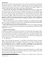
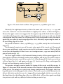
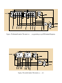
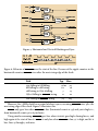
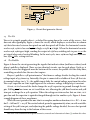
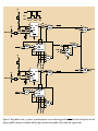
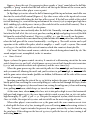
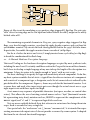
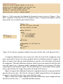
Reconstructing Pong on an FPGA
Stephen A. Edwards
Department of Computer Science, Columbia University
cucs–023–12, December 2012
Abstract
I describe in detail the circuitry of the original 1972 Pong video arcade game and how I
reconstructed it on an fpga—a modern-day programmable logic device. In the original
circuit, I discover some sloppy timing and a previously unidentified bug that subtly affected
gameplay. I emulate the quasi-synchronous behavior of the original circuit by running a
synchronous “simulation” circuit with a 2× clock and replacing each flip-flop with a circuit
that effectively simulates one. The result is an accurate reproduction that exhibits many
idiosyncracies of the original.
1
Pong Circuit Description
1.1 The Main Clock . . . . . . .
1.2 The Horizontal Counter . . .
1.3 The Vertical Counter . . . .
1.4 Horizontal and Vertical Sync
1.5 The Net . . . . . . . . . . . .
1.6 The Paddles . . . . . . . . . .
1.7 The Score . . . . . . . . . . .
1.8 Horizontal Ball Control . . .
1.9 Vertical Ball Control . . . . .
1.10 Video Generation . . . . . .
1.11 Sound . . . . . . . . . . . . .
1.12 Game Control . . . . . . . .
.
.
.
.
.
.
.
.
.
.
.
.
2
2
2
5
5
7
7
9
11
15
17
17
19
2
Reconstructing Pong on an FPGA
2.1 Handling Quasi-Synchronous Circuits . . . . . . . . . . . . . . . . . . . . . .
2.2 A Minimal Hardware Description Language . . . . . . . . . . . . . . . . . . .
2.3 I/O on the Terasic de2 board . . . . . . . . . . . . . . . . . . . . . . . . . . . .
21
21
22
25
3
Conclusions
26
.
.
.
.
.
.
.
.
.
.
.
.
.
.
.
.
.
.
.
.
.
.
.
.
.
.
.
.
.
.
.
.
.
.
.
.
.
.
.
.
.
.
.
.
.
.
.
.
.
.
.
.
.
.
.
.
.
.
.
.
.
.
.
.
.
.
.
.
.
.
.
.
.
.
.
.
.
.
.
.
.
.
.
.
.
.
.
.
.
.
.
.
.
.
.
.
.
.
.
.
.
.
.
.
.
.
.
.
.
.
.
.
.
.
.
.
.
.
.
.
.
.
.
.
.
.
.
.
.
.
.
.
.
.
.
.
.
.
.
.
.
.
.
.
.
.
.
.
.
.
.
.
.
.
.
.
.
.
.
.
.
.
.
.
.
.
.
.
.
.
.
.
.
.
.
.
.
.
.
.
.
.
.
.
.
.
.
.
.
.
.
.
.
.
.
.
.
.
.
.
.
.
.
.
.
.
.
.
.
.
.
.
.
.
.
.
.
.
.
.
.
.
.
.
.
.
.
.
.
.
.
.
.
.
.
.
.
.
.
.
.
.
.
.
.
.
.
.
.
.
.
.
.
.
.
.
.
.
.
.
.
.
.
.
.
.
.
.
.
.
.
.
.
.
.
.
.
.
.
.
.
.
.
.
.
.
.
.
.
.
.
.
.
.
.
.
.
.
.
.
.
.
.
.
.
.
.
.
.
.
.
.
.
.
.
.
.
.
.
.
.
.
.
.
Introduction
This work started with a desire to play Pong, Atari’s 1972 video arcade game that effectively
launched the industry [11]. While I could have sought out one of the few remaining machines,
I chose instead to reconstruct it on an fpga, much as I had done for the Apple II computer [7]
and others have done for various other classic video arcade games [8].
Pong and other early games were implemented largely with discrete ttl chips, hence
my choice of an fpga. By contrast, most later games were processor-based and have been
successfully emulated in software using an instruction-set simulator interacting with a highlevel ad hoc simulator for the video hardware [9]. While modern processors are vastly
faster than the roughly 7 MHz clock frequency of Pong and many have written Pong-like
programs in software, my goal was precise (cycle-accurate) emulation. I ruled out doing so in
software because I expect it would be difficult to implement a software circuit simulator able
to consistently run this fast.
However, while the Pong circuit is ostensibly synchronous, it is actually littered with ripple
counters, rs latches built from discrete nand gates, and flip-flops clocked from combinational
logic, all of which are anathema to robust fpga designs.
Below, I describe the circuit of the original Pong with a focus on its timing and analog
components (§ 1), then describe my technique for reconstructing it on a modern-day, fully
synchronous fpga (§ 2).
1
Pong Circuit Description
In addition to reading the schematics for Pong that can be found online (they appear to have
been scanned from service manuals), Dan Boris [4] presents an extensive description of the
circuit; much of what I write here is derived from his work, especially his division of the
circuit into sections. Arkush [15] also describes part of the circuitry in Pong, focusing closely
on how counters are used to control the position of the ball.
1.1 The Main Clock
Figure 1 shows the main clock generator: a 14.318 MHz crystal oscillator1 driving a nand gate
driving a jk flip-flip that halves the frequency and generates a 50% duty-cycle square wave:
the 7.159 MHz master clock. 14.318 MHz is a common crystal frequency in video circuits
because it is four times the ntsc colorburst frequency of 315/88 MHz = 3.579545 MHz. Pong,
however, is black-and-white so another frequency could have been used.
1.2 The Horizontal Counter
The horizontal counter (Figure 2), built from two 7493s (f8 and f9) and a 74107 (f6), keeps
track of the horizontal position of the video beam. The 7493 is a four-bit ripple counter built
from four negative-edge-triggered t flip-flops.
1
The frequency is not labeled on the schematic, but multiple sources, including schematics of Pong clones,
confirm this value.
14.318 MHz
100pF
330 Ω
330 Ω
11
C9e
10
0.1 µ F
9
7404
C9d
8
7404
12
E6d
13 7400
11
1
3
1
J Q
12 F6a
4 74107 2
1
K Q
13
CLK
1
Figure 1: The main clock oscillator. This generates a 7.159 MHz square wave.
Abstractly, the eight-input nand f7 detects the count 256 + 128 + 64 + 4 + 2 = 454 and
causes the counter to reset, but the behavior is slightly more subtle, as shown in Figure 4.
Because the ripple counters are triggered on the negative edge of the clock but the output of
f7 is buffered by the positive-edge-triggered d flip-flip e7b, the count 454 is only seen for half
a clock period while the count 0 is seen for one-and-a-half clock periods because the hreset
signal only rises after the next rising edge of the clock, effectively surpressing the count on
the next falling edge of the clock.
The period of hreset is thus 7.159 MHz/455 = 15.734 kHz, exactly the ntsc horizontal
frequency.
The horizontal counter is one of the most active parts of the circuit, yet Alcorn used
slower, more problematic ripple counters instead of synchronous counters. Why he did this
is not clear; one hypothesis is that it was a cost-saving measure: 7493s were nearly half the
price of 74161s in 1975 [10].
The use of ripple counters in the horizontal timing circuitry of these games appears to be
characteristic of Alcorn. Bushnell’s earlier, more complex, and far less successful Computer
Space (Nutting Associates, 1973) did use 74161s [12]. Alcorn designed [6] Atari’s 1973 successor
to Pong, Space Race [11], and again used 7493s [3]. Atari’s 1974 Pin Pong, not designed by
Alcorn, used synchronous counters (9316s) [2].
The presence of ripple counters makes the timing of this circuit worth discussing. In
Figure 2, I drew some of the internal structure of the counters to help explain the behavior
of this circuit. The outputs 1h...256h do not change simultaneously: they ripple, which can
be problematic for decoding particular columns. To decode 454 as needed, fortunately, the
delay is effectively modest because it is triggered by 2h going high, which occurs only two
flip-flop delays after the falling edge of the 7.159 MHz clock—all the other signals went high
in a previous cycle and stay stable just before reaching a count of 454.
CLK
14
3
7493
12
2
F8
1
9
8
11
14
3
7493
12
2
1
F9
9
8
1
8
5
J Q
9 F6b
11 74107 6
K Q
256H
10
11
1
256H
128H
64H
32H
16H
8H
4H
2H
1H
1
11
12
5
F7
6 7430
2
3
4
10
812
9
D Q
11 E7b
7474 8
Q
HRESET
HRESET
13
Figure 2: The horizontal counter: This counts 0, 1, . . . , 454, generating a 15.734 kHz horizontal frequency.
HRESET
14
1
3
2
3
2
R02 R01
R02 R01
14
CKA E8
CKA E9
1
CKB 7493
CKB 7493
QA QB QC QD
QA QB QC QD
12 9 8 11
12 9 8 11
1
8
5
J Q
9 D9b
11 74107 6
K Q
256V
10
9
10 D8c
11 7410
4
82
5
D Q
3 E7a
7474 6
Q
1
256V
128V
64V
32V
16V
8V
4V
2V
1V
Figure 3: The vertical counter: This counts 0, 1, . . . , 261
1
VRESET
VRESET
CLK 7M
1H-256H
451
452
453
454
0
2
3
HRESET
HBLANK
1V-256V
261
0
VRESET
1V-256V
0
1
1
2
VRESET
1V-256V
VRESET
Figure 4: Behavior of the horizontal and vertical counters at the end of a horizontal line
1.3 The Vertical Counter
The vertical counter (Figure 3) is similar to the horizontal counter, but is clocked once per
field by the hreset signal generated by the horizontal counter and resets on a count of
1 + 4 + 256 = 261. This gives a vertical refresh frequency of 15.734 kHz/262 = 60.05 Hz, which
is certainly close enough to 60 Hz for most monitors. A strictly compliant (interlaced) ntsc
signal actually has 525/2 = 262.5 horizontal line periods per field.
Again the 7493s are negative-edge triggered, so the vertical count changes when hreset
falls and is reset when hreset rises—see Figure 4.
1.4
Horizontal and Vertical Sync
Figure 5 shows the circuits for generating horizontal and vertical blanking and synchronization
signals. These are two rs latches built from discrete gates with some extra gating logic.
Part of the timing of the horizontal blanking latch is problematic. The hreset signal
is not a problem because it comes directly from a flip-flop triggered by the clock (e7b, see
Figure 2, so hblank falls quickly after the rising edge of the clock. However, for hblank to
rise, 64h must be high and nand g5b looks for the rising edge of 16h (a count of 64 + 16 = 80).
This is initiated by a falling edge on the 7 MHz clock and occurs after passing through five
flip-flop stages (all of the f8 ripple counter and the first stage of f9). Below is an accounting
of delays based on numbers from ti’s 1988 data book [14].
16H
64H
3
4 G5b
5 7410
HRESET
64
H5b
5 7400
6
9
H5c
10 7400
8
32H
VRESET
16V
8
9
F5c 10
7402
11
12
F5d 13
7402
4V
8V
1
H5a
2 7400
3
HBLANK
12
H5d
13 7400
HBLANK
11
HSYNC
VBLANK
1
2 G5a
13 7410
VBLANK
12
VSYNC
Figure 5: Horizontal and Vertical Blanking and Sync
CLK 7M
1H-256H
77
78
79
80
81
82
HBLANK
Figure 6: Behavior of hblank near the start of the line. Because of the ripple counters in the
horizontal counter, hblank rises after the next rising edge of the clock.
Path
Typ.
Max.
clk falling to 8H falling
8H falling to 16H rising
16H rising to G5b-6 falling
G5b-6 falling to hblank rising
46 ns
10
7
11
70
16
15
22
clk falling to hblank rising
74
123
However, the 7 MHz clock has a period of about 140 ns, meaning hblank rises after the
next rising edge of the clock. Figure 6 illustrates this.
hsync only goes low when hblank is low (horizontal counts 0–79) and 32h is high, i.e.,
from horizontal counts 32 to 63 inclusive.
Using similar reasoning, vblank goes low when vreset goes high: during line 0, and
high again at the start of line 16. vsync is only low when vblank is low, 4v is high, and 8v is
low: lines 4 through 7 inclusive.
VBLANK
V4
256H
CLK
256H
4
G3b
5 7400
5
8
J Q
9 F3b
11 74107 6
K Q
10
6
3
4
5
G2b 6
7427
NET
1
Figure 7: Circuit that generates the net
1.5
The Net
The net is a simple graphic object—a dashed line going down the center of the screen—that
does not affect gameplay. Figure 7 shows the circuit, which displays a vertical line in column
256 that alternates between four pixels on and four pixels off. Before the horizontal counter
reaches 256, 256h is low and 256h is high, so f3b’s q is high. When the horizontal counter
reaches 256, 256h goes high, sending the output of g3b low, enabling g2b to pass v4 as the
net signal when out of vertical blanking. In the next cycle, since 256h was high and 256h was
low, f3b’s q falls, setting net low.
1.6 The Paddles
Figure 8 shows the circuit generating the signals that indicate when (and hence where) each
player’s paddle is displayed. There are two identical circuits, one for each player. Each 555 is
wired as a one-shot triggered near the bottom of the screen; the paddle sets the delay time,
controlling on which line the one-shot expires.
Player 1’s paddle is a 5K potentiometer2 that forms a voltage divider feeding the control
voltage input of 555 timer b9. Internally, this pin is connected to a ladder of three 5K that sets
its nominal voltage to 2/3 Vcc ; the paddle input shifts the control voltage away from this value.
The 0.1µF capacitor on ctrl input bypasses the reference voltage to help keep it constant.
At rest, out is low and the diode clamps the 0.1µF capacitor to ground through the dis
pin. Pulling trg low turns on out and floats dis, allowing the 56K fixed resistor and 50K
trim pot to charge the 0.1µF capacitor. When the voltage on thr reaches that on ctrl, out
goes low and the capacitor is again discharged through dis for another cycle. Figure 8 shows
a rough diagram of these waveforms.
While the exact period of the one-shot is a complex, nonlinear function, it is ≈ RC = 8.1ms
for R = 81K and C = 0.1µF. The vertical refresh period is approximately 16ms, so with a suitable
setting of the 50K trim pot, and adjusting the paddle voltage divided, the one-shot period
should vary from the top to the bottom of the screen.
2
This value is not marked on the original schematics; manuals and schematics of clones [1] confirm this value.
+5
TRG
50K
OUT
THR
56K
PADDLE 1
5K
0.1 µ F
+5
14
470 Ω 256V
0.1 µ F
C9b
6
3 3
4 1
THR
OUT
B7a
7
2 7400
7404
DIS B9
2
TRG 555
5
CTRL
RST
HSYNC
5
B7b
4 7400
4
6 14
1
128H
4H
8
9
B7c
10 7400
8 14
1
11
10
9
G2c 8
7427
PAD1
13
2
1
G2a 12
7427
PAD2
8
2
5
D Q
3 H3a
7474 6
Q
1
D1
0.1 µ F
6
3 1
2 13
THR
OUT
B7d
7
7404 12 7400
DIS A9
2
TRG 555
5
CTRL
RST
4
10
G3c
9 7400
4
1
C9a
470 Ω 256V
HSYNC
C1
B1
0.1 µ F
18
ATTRACT
9
10
A7b
12 7420
13
56K
5K
256H
3
2
R02 R01
CKA B8
CKB 7493
QA QB QC QD
12 9 8 11
50K
PADDLE 2
VPAD1
1
+5
+5
3
11
VPAD2
256H
1
3
2
R02 R01
CKA A8
CKB 7493
QA QB QC QD
12 9 8 11
1
2
A7a
4 7420
5
6
D2
C2
B2
Figure 8: The paddle circuit. 555 timers a9 and b9 operate as one-shots triggered by 256v that select the top line of each
player’s paddle. Counters a8 and b8 and flip-flop h3a make each paddle 15 lines high and 4 pixels wide.
However, Alcorn explains,
The other—not hack—but, one of my lessons learned, is that if you can’t fix it,
call it a feature. The paddles on the original Pong didn’t go all the way to the top.
There was a defect in the [circuit]—I used a very simple circuit, I had to, to make
the paddles, but they didn’t go to the top. I could have fixed it, but it turned out
to be important, because if you get two good players they could just volley and
play the game forever. And the game has to end in about three or four minutes
otherwise it’s a failure as a game. So that gap at the top, again—a feature. So that
was sort of a happy accident. [13]
Going higher on the screen corresponds to a shorter timeout, which in this circuit is
limited in part by how low the voltage can go on ctrl, which is affected by the internal 5K
resistor ladder.
While the 555’s out is high, the paddle is not displayed because the the output of B7a
stays high, pad1 stays low, and the four-bit ripple counter b8 is reset.
The paddle starts to be displayed on the line where out first goes low and continues to be
displayed for the next fourteen lines. Here, both the output of inverter c9b and the output of
a7b are high, so vpad1 is low. The output of a7b stays high until the counter reaches fifteen.
b7b clocks it on the rising edge of hsync. On the count of fifteen, the output of a7b falls
sending b8’s clock a high. This is a glitch: the output of b7b falls, causing qa to rise, causing
the output of a7b to fall, which finally causes the output of b7b to rise again. However, the
7493 only requires a 15 ns pulse on clka for proper operation and the delay from clka to qa
is typically 10 ns and the delay through a 7420 is typically 8 ns, so it should work.
The three higher-order output bits of each paddle’s vertical counter are used to determine
the angle at which the ball bounces off the paddle; see § 1.9.
Together, h3a and g3c determine the horizontal width and position of the paddle: the
output of g3c goes low between the rising edge of 128h (horizontal counts 128 and 384) and
the next rising edge of 4h (horizontal counts 132 and 388) to give a four-pixel-wide paddle.
This occurs twice per line, once when 256h is low, displaying the left paddle through g2c, and
once when 256h is high, displaying the right through g2a.
1.7
The Score
Pong displays two two-digit scores in “seven-segment” style on the upper part of the screen.
Each player’s score is held in a decade ripple counter for the first digit augmented with a jk
flip-flop to represent the tens digit. A switch controls whether the game ends when either
player reaches a score of 11 or 15.
At the core of the circuit is a 7448 bcd-to-seven-segment decoder, which was originally
designed to drive seven-segment led displays. In Pong, a pair of four-to-one multiplexers
steer one of the four score digits to the 7448, which feeds the decoded number into a bank of
seven nand gates that are each activated during a “segment” region on the screen. Finally,
HVID
1
2
H6a
4 7420
5
MISS
D1f
8 13
12 1
E1a
2 7400
7404
6 9
E6c
10 7400
11 SW1A S1A
S1C
3
HBLANK
ATTRACT
L
6
5
MISSED
F5b 4
7402
SRST
0
0
S1E
3
11 SW1B S2A
4 D8b
S2C
5 7410
15
S2E
F5a 1
0 0
7402
3
2
R
15
1
2 D8a
13 7410
2 3
6 7
1
3
J Q
S1E
14 R01 R02 R91 R92 1
CKA C7
12 C8a
1
CKB 7490
4 74107 2
K Q
S1E
QA QB QC QD 1
12 9 8 11
13
12
1
B2a
2 7400
3
STOP G
6
2 3
6 7
8
5
J Q
S2E
14 R01 R02 R91 R92 1
CKA D7
9 C8b
1
CKB 7490
11 74107 6
K Q
S2E
QA QB QC QD 1
12 9 8 11
10
SRST
S1A S1B S1C S1D
S2B
S2E
S1A
S1B
1
S1E
6 5 4 3
10 11 12 13
0 1 2 3
0 1 2 3
14
1
0
A
1G
C6
2
15
74153
0
B
2G
1Y
2Y
7
9
1
32H
64H
S2A
32V
256H
64H
128H
1
2
13
3
4
5
E3a 12
7427
E3b 6
7427
9
10 E2c
11 7410
9
8 10
11
E3c 8
7427
E4c
7404
12
C3d
13 7400
4H
8H
3
E4b
7404
11
5
6
3
4
5
4
1
2 E2a
13 7410
12 1
E5c 8
7427
D2b 4
7402
E5b 6
7427
E4a
7404
G1a 1
7402
64V
128V
5
9
10
11
4V
8V
S2C
S2D
S2E
S2E
S1C
S1D
S1E
S1E
6 5 4 3
10 11 12 13
0 1 2 3
0 1 2 3
14
1
0
A
1G
D6
2
15
74153
0
B
2G
1Y
2Y
7
9
2
3
16V
16H
S2A S2B S2C S2D
2
6
8
9
D2c 10
7402
1
2
f
13
e 9
10
11
9
10
11
b
1
c 2
13
a 9
10
11
g 3
4
5
3
4
5
d
1
2
4
5
F2a 6
7425
4
5
0
3
0
64H 32H
0
0
1
1
0
1
0
1
D C B A
1111, 0001 when player one ≥ 10
Low four bits of player one's score
1111, 0001 when player two ≥ 10
Low four bits of player two's score
7 1 2 6
A B C D
BI/RBO
C5
RBI
7448
LT
a b c d e f g
13 12 11 10 9 15 14
a b c d e f g
4H
D4a
7410
12
D5c
7410
8
C4c
7410
8
D5a
7410
12
D4c
7410
8
D4b
7410
6
D5b
7410
6
4H
a
4V
f
4V
12
4V
5
4
1
8
D3
2 7430
1
11
6
3
b
g
4V
e
8V
c
8V
d
16V
8H
SCORE
Figure 9: Score circuitry: the outputs of f5b and f5a pulse when a player has scored; c7, c8a, d7, and c8b maintain the score; the
remainder displays the score as two two-digit seven-segment decimal numbers.
the output of these gates are fed into an eight-input nand gate that effectively sums them to
produce the final score display signal, which is mixed to produce a slightly dimmer display
than the signal for the ball, paddles, and net.
Starting from the top left of Figure 9, hvid is low where the ball is present (see § 1.8), so
miss goes low when the ball reaches the horizontal blanking region (i.e., off the left or right
of the screen). When the game is not in attract mode, this causes the missed signal to go low,
sending the clock of either c7 or d7 high. If the ball was moving left when this happens (i.e.,
past player one), R will be low, pulsing the clock of d7 high. When it falls, player two’s score
counter (d7) will increment.
Player one’s score counter consists of the four-bit ripple decade counter c6 and jk flip-flop
c8a. After c7 reaches a count of nine, it will reset itself to zero on the next cycle, dropping qd
and causing c8a to toggle, indicating a score of ten. Player two’s score counter (d7 and c8b) is
wired similarly.
Nand gates d8a and d8b detect the end-of-game condition, dictated by sw1. In its “11”
position, the inputs to d8a and d8b float high, meaning stop g will rise when either player
reaches a score of 11. Similarly, when sw1 is in the “15” position, the first, third, and fifth bits
of the score must be one: a score of 15.
Depending on horizontal counter values 32h and 64h, four-input muxes d6 and c6 steer
either the low digit of each player’s score, 1 when the high-order bit of a player’s score is 1,
or 15 when it is zero, to the seven-segment decoder c5. The 7448 turns off all digits when fed
an input of 15, so this logic disables a leading zero.
Gates e3a, e3b, e2c, e3c, g1a, d2a, and f2a enable the outputs of c5 when the beam is over
the score area at the top of the screen.
Gates e4b, c3d, e5c, d2b, e5b, e4a, and e4c compute functions for displaying the segments
as shown on the map on the left of Figure 9. Consider the output of d4b. It drives the output
of d3 high when g is high, 4v and 8v are high, 16v is low, and 16h is high. This produces the
horizontal bar that appears above the midpoint as shown in the diagram. It turns out 16h
must be high for any segment to be visible; the constraints on 4v, 8v, 16v, 4h, and 8h vary
depending on the segment.
1.8
Horizontal Ball Control
To control the position of the ball, Pong uses a clever technique described in Bushnell’s 1974
patent [5] that involves running “position” counters at almost the same frequency as the
horizontal and vertical counters. In such a situation, the phase of these “position” counters
relative to the main horizontal counters determine where on the screen the ball will appear;
slight perturbations to the period of the position counters cause the ball to move.
Figure 10 shows the circuit responsible for the horizontal position of the ball. This is built
around a nine-bit counter built from g7, h7, and g6b, which reloads itself when it reaches a
count of 511.
8
9
256H
VRESET
RST SPEED
HIT SOUND
12
E1d
13 7400
Hits
3
2
R02 R01
11 14
CKA F1
1
CKB 7493
QA QB QC QD
12 9 8 11
11
12
8
1
G1d 13
H1a
2 7400
7402
1
H4a
8
5
1
3 2 7400
J Q
J Q
9 H2b
12 H2a
11 74107 6
4 74107 2
K Q
K Q
11/MOVE
10
0 13
H1-8 6
03
411
12
9
E1c
10 7400
G1c 10
7402
1
01
10
00
13
H1d
12 7400
9
H1c
11 10 7400
8
4
H1b
5 7400
6
3
3
01/MOVE
10/MOVE
00/MOVE
MOVE
HIT2
SC
ATTRACT
HIT1
10
12
C1d
13 7400
D1a 12 D Q 9
11 1
2 11 H3b
7474 8
7404
Q
L
12
H4d
13 7400
4
H4b
5 7400
13
11 9
H4c
10 7400
6
Ba
R
HBLANK
CLK
ATTRACT
SERVE
9
1
3 4 5 6
A B C D
7 LD
ENP
2
15
7
G7
CLK 9316 RCO
10
2
ENT
10
CLRQA QB QC QD
1
1 14 13 12 11
4
E1b
5 7400
6
LR
Aa Ba
Range
Period
Movement
0
1
1
10
01
01
11
10
138,. . . ,511
139,. . . ,511
137,. . . ,511
374
373
375
Stationary
Left
Right
Aa
0
1
MOVE
8
0
0
0
1
9
3 4 5 6
LD A B C D
8
1
ENP
15
9
H7
CLK 9316 RCO
11
1
ENT
CLRQA QB QC QD
1 14 13 12 11
5
Q
G6b
74107 6
K Q
J
9
10 G5c
11 7410
8
9
10
H6b
12 7420
13
8
10
HVID
Figure 10: Ball horizontal circuit. The output, hvid, is asserted when the ball is visible in the current column. Four-bit counter F1
counts hits and speeds up the ball in response. The duration of the MOVE signal controls how many pixels to move the ball left or right.
Finally, the phase of the nine-bit counter formed by G7, H7, and G6b determines the horizontal position of the ball.
When the move signal is low, the horizontal ball counter stays in phase with the master
horizontal counters, in effect keeping the ball in the same horizontal position. When move is
low. h4b, h4c, and h4d set Aa and Bb, inputs to the synchronous four-bit counter g7 (a 9316,
pin compatible with the more familiar 74161 chip), to 0 and 1 respectively. Thus, when the
horizontal ball counter reaches 511, the output of g5c goes low and the counter is loaded with
the value 010001010 = 128 + 8 + 2 = 138 on the next rising edge of the clock (h7’s rco falls
when this value is loaded, toggling G6b, which becomes a 0 because it was a 1 to activate g5c).
In this mode, therefore, it counts 138, 139, . . . , 511: a period of 374.
The horizontal ball counter only advances on rising edges of the clock when hblank is
high since hblank drives g7’s ent input. From the discussion in § 1.4, this occurs during
horizontal counts 81, 82, . . . , 454: 374 times per line. Thus, when move is low, the horizontal
ball counter stays in sync with the horizontal counters.
The hvid signal indicates the position of the ball. It is asserted when the horizontal ball
counter has values 111111100–111111111, i.e., 508, 509, . . . , 511, making the ball four pixels wide.
When move is high, the horizontal ball counter resets to a slightly different value, effectively making the ball move left or right. h3b, a d flip-flop, controls the direction. When l is 1,
r is 0, Ba is 1, and Aa is 1, making the counter reset to 128 + 8 + 2 + 1 = 139. This makes the
period one less then the duration of hblank, moving the ball to the left.
Conversely, when move is high and l is 0, r is 1, Ba is 0 and Aa is 1, making the counter
reset to 128 + 8 + 1 = 137 and moving the ball to the right.
H3b makes the ball bounce off the players’ paddles. When the left paddle (player one)
touches the ball, hit1 goes low, setting h3B into a state where L=0 and R=1, thus sending the
ball right. Similarly, colliding with player two’s paddle sends the ball left. Note that because
these signals set the direction of the ball, rather than change it, there is no danger of the ball
becoming trapped inside a paddle that suddenly appears from being moved very quickly.
H3b also makes the ball bounce off the left and right edges of the screen in attract mode.
The sc signal pulses high for a few clock cycles when the ball goes off the screen horizontally
(i.e., causing a score if the game were being played). In attract mode, c1d passes this pulse
through to h3b’s clock, causing it to toggle once when the ball hits the edge of the screen.
Ripple counter f1 counts the number of hits, which is used to increase the (horizontal)
speed of the ball. rst speed goes high briefly during game play when one player scores a
point, resetting counter f1. After reset, qc and qd are low, setting e1c’s output high. Thereafter,
when hit sound pulses high (when the ball hits either paddle), it clocks f1. Once f1 reaches
a count of 8 + 4 = 12, e1c’s output goes low, inhibiting further counts until the next point.
The output of counter f1 is decoded to control the clear inputs of jk flip-flops h2a and
h2b, which form a state machine that controls whether move is asserted on one, two, or three
lines per field, controlling the horizontal speed of the ball. Figure 10 shows the state transition
diagram for this machine, which is clocked on the falling edge of 256h except on the first
line of each field (when vreset is high), when nand gates h1b and h1c set the state of this
machine.
1
3
J Q
12 A2a
4 74107 2
K Q
VVID
VBLANK
HIT
D1
256H
D2
256H
C1
C2
B2
B1
ATTRACT
HIT
A2B5A5A5
a a a b
13
3
2 B6b
4
5 7450
6
6
7404
0
0
0
0
0
0
0
0
1
1
1
1
1
1
1
1
8
1
4
2
5
D Q
3 A5a
7474 6
Q
4
A4b 6
5 7486
1
1
13 A6a
9
10 7450
5
1
13 B6a
9
10 7450
1
3
2 A6b
4
5 7450
D1c
1
4
2
5
D Q
3 B5a
7474 6
Q
8
6
10
12
9
D Q
11 A5b
7474 8
Q
13
1
2 C4a
13 7410
1
9
A4c 8
10 7486
12
0
1 1 0
10 8 3 1
11 7 4 16
A1 A2 A3 A4 B1 B2 B3 B4
13
14
B4
0
C0
C4
7483
Σ1 Σ2 Σ3 Σ4
9 6 2 15
0
0
0
0
1
1
1
1
0
0
0
0
1
1
1
1
0
0
1
1
0
0
1
1
0
0
1
1
0
0
1
1
0
1
0
1
0
1
0
1
0
1
0
1
0
1
0
1
B4-A
4321
B4-B
4321
Range
0000
0001
0010
0011
0100
0101
0110
0111
0111
0110
0101
0100
0011
0010
0001
0000
0111
0111
0111
0111
0110
0110
0110
0110
0110
0110
0110
0110
0111
0111
0111
0111
7,. . . ,255
8,. . . ,255
9,. . . ,255
10,. . . ,255
10,. . . ,255
11,. . . ,255
12,. . . ,255
13,. . . ,255
13,. . . ,255
12,. . . ,255
11,. . . ,255
10,. . . ,255
10,. . . ,255
9,. . . ,255
8,. . . ,255
7,. . . ,255
Ab Bb Cb Db
9
HSYNC
VBLANK
3 4 5 6
A B C D
LD
7
1
ENP
2
15
B3
CLK 9316 RCO
10
ENT
CLRQA QB QC QD
1 14 13 12 11
1
0 0 0 0
3 4 5 6
A B C D
7 LD
ENP
2
15
A3
CLK 9316 RCO
10
1
ENT
CLRQA QB QC QD
1 14 13 12 11
9
4
B2b
5 7400
5
4 E2b
3 7410
1
6
VBALL240
VVID
6
11
12
D2d 13
7402
VVID
VBALL32
VBALL16
Figure 11: Ball vertical circuit. The output, vvid, is asserted when the ball is visible on the current line. Flip-flops b5a, a5b, and a5b remember the position at
which the ball last hit a paddle; a2a toggles to rebound the ball off the top or bottom. Four-bit adder b4 translates the ball motion signals into a reset value for the
eight-bit counter formed by a3 and b3, which determines the vertical position of the ball.
1.9
Vertical Ball Control
Figure 11 shows the circuit responsible for the vertical position of the ball. Like the horizontal
circuit, it consists of a counter (only eight bits for the vertical counter: a3 and b3) whose
period, and hence vertical ball speed, is set by a state machine affected by a ball hitting a
paddle or the top or bottom of the screen.
When the game is in attract mode, the paddles are hidden and the ball travels at one
speed diagonally, bouncing off the sides of the screen. In this state, inverter d1c drives the
clear inputs of d flip-flops b5a, a5a, and a5b, setting their q’s to all 0.
Jk flip-flop a2a, together with exclusive-or gates a4b, a4c, and b6a (an and-or-invert
gate wired to compute exclusive-or) are responsible for bouncing the ball off the top and
bottom of the screen. When a2a’s q is low, the exclusive-or gates pass the outputs of the three
d flip-flops unchanged and invert them when the q output is high. The state of a2a toggles
when the ball hits the screen top or bottom: when vvid is high (i.e., when the ball is visible
on the current line) at the end of vertical blanking (when vblank falls).
As in the horizontal circuit, the phase of the vertical counter (formed by synchronous
four-bit counters a3 and b3) affects the vertical position of the ball and the period of the
counter affects the ball’s vertical velocity. Here, however, the counter is clocked by the rising
edge of hsync and gated by vblank. As discussed in § 1.4, there are 262 lines per field and
vblank is active for 16 of them, giving the ball vertical counter 262 − 16 = 246 counts per
field. Thus loading the vertical ball counter with 10 will hold the ball in the same position
vertically; smaller numbers increase the period, causing the ball to move down on the screen;
larger numbers will cause it to move up. In attract mode, the counter is loaded with 7 or 13
depending on a2a, so it will move at the maximum speed vertically.
During gameplay, the ball rebounds off the paddle at an angle determined by where the
ball hit the paddle. d flip-flops b5a, a5a, and a5b remember this collision location; binary
adder b4 transforms it into a value with which to load the ball vertical counter.
When the ball hits the paddle, hit pulses high, resetting a2a and loading d flip-flops b5a,
a5a, and a5b with the one’s complement of the top three bits of one of the paddle counters
(see § 1.6). And-or-invert gates a6a, a6b, and b6b are wired as two-input multiplexers that
pass the top three bits of player one’s paddle position (b1, c1, and d1) when 256h is low (i.e.,
the ball is to the left of the net) and player two’s paddle position when 256h is high.
In the table in Figure 11, note that the range 10,. . . ,255 appears four times instead of two.
This makes it easier to rebound the ball purely horizontally—there is a large area in the center
of the paddle where this will happen.
It appears the inputs to a6a are wired incorrectly. While b6b and a6b select data from
player one when 256h is low as we would expect, a6a selects data from player two. The
schematic in Figure 11 is consistent with the original schematics (Figure 12) as well as the
board.3 Even the schematic for an (unauthorized) clone of Pong has this error [1].
3
I traced the signals on a high-resolution photo of the front and back of the two-layer board.
Figure 12: Part of Pong’s original schematic: the vertical ball counter. The intention of the top
and-or-invert gate (a6) is clear: pass b1 under the same conditions as c1 and d1, but pins 1
and 10 are swapped: pins 1 and 13 are one group; 9 and 10 are the other.
1.2K
SCORE
E4e
12
10 2.2K
A4d 11 11
13 7486
7404
HSYNC
VSYNC
9
10
12
13
PAD1
NET
PAD2
HVID
VVID
5
6
G1b 4
7402
F2b 8 13
7425
1
G3a
2 7400
12
G3d
13 7400
E4f
12
B2d
13 7400
3
11
20 Video Out
12 1K
7404
9
10
5 µ F 10V
11
HIT
HIT2
B2c
7400
8
HIT
HIT1
Figure 13: Video generation circuitry. F2b combines the signal from the two paddles, the net,
and the ball. The score display is mixed with a 1.2K resistor, making it slightly dimmer.
1.10
Video Generation
Figure 13 shows the circuit that combines the horizontal and vertical synchronization signals
(§ 1.4), the net (§ 1.5), paddles (§ 1.6), score (§ 1.7), and the ball (§§ 1.8 and 1.9) to produce
the final composite (black-and-white) video signal. A resistor summing network combines
the score, sync, and other video elements. Note a higher-value resistor is used for the score
(1.2K); this makes it slightly dimmer than the paddles, ball, and net. A 5µF coupling capacitor
removes any dc bias.
Also in Figure 13 is the logic generating hit, hit1, and hit2, used, e.g., by the ball vertical
circuit.
1.11
Sound
The sound in Pong is legendarily simple, perfect, and almost serendipitous, as Alcorn relates:
Now the issue of sound . . . People have talked about the sound and I’ve seen
articles written about how intelligently the sound was done and how appropriate
the sound was. The truth is, I was running out of parts on the board. Nolan
wanted the roar of a crowd of thousands—the approving roar of cheering people
when you made a point. Ted Dabney told me to make a boo and a hiss when you
lost a point, because for every winner there’s a loser.
I said, “Screw it, I don’t know how to make any one of those sounds. I don’t
have enough parts anyhow.” Since I had the wire wrapped on the scope, I poked
around the sync generator to find an appropriate frequency or a tone. So those
sounds were don in half a day. They were the sounds that were already in the
machine. [11]
ATTRACT
4
C3b 6
1
3
5 7400
J Q
12 F3a
4 74107 2 Top Hit Sound
K Q
VBALL32
VVID
VBLANK
VVID
6
4
C1b
5 7400
6
16 SOUND
13
SERVE
4
1
VBALL240
1
2
5
D Q
3 C2a
7474 6
Q
Hit Sound
1
C3a
2 7400
1
HIT
VBALL16
+5
3
4 C4b
5 7410
HIT SOUND
3
32V
220K
1.0
MISS
0.1
6
3
THR
OUT
7
DIS G4
2
TRG 555
5
CTRL
RST
4
9
C3c
10 7400
8
SC
Score Sound
0
Figure 14: Sound Circuitry
Figure 14 bears this out. Pong generates three sounds: a “ping” sound when the ball hits
a paddle, a “pong” sound when the ball reflects off the top or bottom of the screen, and a
similar sound when either player scores a point.
Jk flip-flop f3a is active when the ball is bouncing off the top or bottom, much like a2a
does for the vertical ball control (Figure 11). F3a takes a new value at the top of each screen
(i.e., when vblank falls before the first line of the screen). If the ball was visible at the end of
vertical blanking (i.e., went off the top or bottom of the screen), f3a’s q output goes high for a
field, enabling c3b, which passes vball32 (the sixth bit of the vertical ball counter). This is
15.734 kHz / 16 = 980 Hz, near B5 on the piano.
D flip-flop c2a turns on briefly after the ball is hit. Normally, c2a’s q is low, disabling c3a,
but when the ball is hit, the c2a’s reset goes low, sending q high and gating vball16 (the fifth
bit from the vertical ball counter). This is 15.734 kHz / 32 = 490 Hz, near B4 on the piano.
Timer g4 activates the score sound for a period of time after miss pulses low, which occurs
when the ball goes off the screen horizontally—see Figure 9. The 220K resistor and 1.0µF
capacitor set the width of the pulse, which is roughly 1.1 ⋅ 220K ⋅ 1.0µF = 240 ms. This sound
is set by 32v, the sixth bit of the vertical counter, which also counts at about 980 Hz.
C4b “sums” the three sound sources, which are silenced during attract mode by c1b. The
sound output is sent, unamplified, to the tv monitor.
1.12
Game Control
Figure 15 shows the game control circuitry. It consists of a debouncing circuit for the coin
switch (inverters c9c and c9f), a latch/power-on reset circuit built from discrete transistors
(q1, q2, and associated resistors and capacitors), and the serve timer (f4).
When the game powers up, the coin switch pulls srst low, srst high, and transistors q1
and q2 remain off, allowing the 100Ω and 300Ω resistors to pull run high, so attract falls
and the game enters attract mode (paddles are hidden, ball bounces off the sides of the screen
instead of causing a score).
Inserting a coin flips the state of the q1-q2 latch to indicate the game is being played: srst
briefly pulses low, resetting the score and pulling q1’s collector low through the 1n914 diode.
This drops the voltage on q2’s base and turns it on, raising the voltage on q1’s base and turning
it on, pulling run down, which keeps q2 turned on after srst rises.
At the same time, when srst pulses low, rst speed pulses high to reset the horizontal
ball speed and triggers 555 f4, the serve timer, which is wired as a one-shot, so f4’s out pulses
high for roughly 1.1 ⋅ 330K ⋅ 4.7µF = 1.7s. This puts the output of e5a low, which asserts serve.
Once out falls, the output of e5a rises and serve falls on the next rising edge of pad1.
When either player’s score reaches 11 or 15, the game ends: the score counters assert stop
g, which pulls the base of q1 low, turning off q2 as well, raising run and asserting attract.
The “Antenna” input is intended to prevent free games initiated by a static shock to, say,
the coin logic. If the voltage on the base of q3 rises, it pulls the base of q1 low, turning it off
and letting run rise.
+5
0.1 µ F
100 Ω
6
SRST
7404
10 12
2
D2a
3 7402
4.7 µ F
E6b 6
7400
1
E6a
2 7400
3
0.1
6
3
THR
OUT
7
DIS F4
2
TRG 555
5
CTRL
RST
4
RST SPEED
15 Antenna
D1b
4
7404
330K
COIN SW
MISS
4
5
3
RUN
+5
Q3
100 Ω
7404
C9c
Q1
SRST
1N914
1N4001
7404
1N914
5
1N914
8
0.1 µ F
12
E4d
220 Ω
C9f
9
STOP G
100 Ω
300 Ω
+5
13
Q2
1
2
13
1
E5a 12
7427
PAD1
1
10
12
9
D Q
11 B5b
7474 8
Q
13
SERVE TIMER
1
Figure 15: Game Control Circuitry
ATTRACT
ATTRACT
SERVE
SERVE
2
Reconstructing Pong on an FPGA
Virtually all of Pong is digital so implementing it on a modern fpga is feasible, but not
straightforward. First, there are a handful of analog sections: the master oscillator; the oneshot timers for the paddles, score, and serve; and the final video output circuitry. Fpgas
typically use external clock oscillators anyway, so this part is easy. The timers can be emulated
with counters. The video circuitry is a primitive d/a converter with four levels: sync, black,
gray, and white. Gray is used for displaying the score; the ball, paddles, and net are all white.
As described earlier, Pong’s sound is actually digital: a 1-bit output produces square waves at
three frequencies.
2.1
Handling Quasi-Synchronous Circuits
Despite utilizing a 7.159 MHz master oscillator, Pong is not classically synchronous. Deviations
from this ideal (i.e., acyclic combinational logic between flip-flips driven by a global clock)
include the ripple counters in the horizontal and vertical circuits, which cause the unexpected
timing of hblank that I described in § 1.4; r-s latches built from discrete gates that generate
horizontal and vertical sync (Figure 5); and numerous flip-flops driven by clocks driven
by derived signals and employing asynchronous set and reset signals. Most of these were
reasonable shortcuts to take in 1972, but are anathema in modern fpga designs.
My solution for reconstructing Pong in a purely synchronous style was to construct
synchronous circuits that essemtially simulate the asynchronous aspects of the original Pong
circuit. My goal was to make the behavior of the reconstructed circuit match the original on
the edges of the 7.159 MHz clock (since parts of Pong are sensitive to both rising and falling
edges) and to assume the absence of glitches on the generated clocks in the original circuit,
i.e., that any switch more quickly than the global clock.
Figure 16 shows the circuit I use to emulate the 7474: a positive-edge-triggered dual d
flip-flop with asynchronous set and reset inputs. I replace each original d flip-flop with three
flip-flops: “q” to hold the current state, “d” to capture the (possibly irrelevant) next state, and
“c” to remember the previous value of the (asynchronous) clock.
This circuit assumes it is clocked fast enough so that neither the clock nor the “d” input
transitions more than once per cycle. The and gate marked “rise” and the “c” flip-flop detect
whether clk has risen since it was last sampled. If clk rose, the mux supplies the value of the
d input sampled before the rising edge by the “d” flip-flop. Otherwise, clk was stable and the
mux delivers the previous value of q, held by the “q” flip-flop. Combinational inputs clr
and pre set and clear the output regardless of the behavior of clk; the feedback loop ensures
their effect is felt in the next cycle even if clk did not rise.
This circuit can simulate the original flip-flop provided it is run at least twice as fast. In
the exactly twice-as-fast case, the clk input is high in alternate cycles and makes the mux
alternate between the “d” and “q” flip-flops, which latches the d input in cycles when clk is
low.
Q
D
CLK
0
1
D
RISE
C
Q
Q
CLR
PRE
Figure 16: My circuit for emulating a 7474 positive-edge-triggered D flip-flop. The and gate
“rise” detects a rising edge on the clk input and either delivers the old Q output or the newly
latched value of D.
The remaining sequential elements in Pong are 74107 negative-edge-triggered jk flipflops, 7493 four-bit ripple counters, 7490 four-bit ripple decade counters, and 9316 four-bit
synchronous counters. My circuits for each closely parallel that for the 7474 I describe above.
In particular, I assemble the ripple counters from a cascade of jk flip-flops.
For the r-s latches for hsync and vsync, I simply inserted a one-cycle delay (a d flip-flop)
to break the combinational feedback loop.
2.2
A Minimal Hardware Description Language
Vhdl and Verilog are the hardware description languages accepted by most synthesis tools,
including the ones I used. I certainly could have written the Pong netlist in one of these formats,
but I chose to develop a simple language of my own to keep the length of the description to a
minimum. I chose its syntax to be simple enough to “parse” with an awk script.
The basic challenge is to specify the type and connectivity of each component. To do this,
my basic syntax resembles that of spice: a typical line describes an instance of a component
and consists of a component type, a designator, and a list of connected nets ordered by the
pins defined for the component. Figure 17 shows my code for the horizontal counter. I cut
a corner here and used a five-input nand gate even though the actual circuit uses a 7430
eight-input nand with three inputs tied high.
A net name is any sequence of printable characters (not space, newline, or control characters). This allows the use of existing, natural names such as “64h” (horizontal counter
bit representing sixty-four), notation such as /HRESET to represent the complement of the
hreset signal, and “0” and “1” to represent logical false and true.
Nets are never explicitly defined; their first reference in an instance line brings them into
scope. Each is assumed to carry a single bit.
One special rule: the “underscore” net (_) means “unconnected;” it is intended for representing unconnected outputs since I do not provide a connect-by-name syntax. I adopted
this from the ml-derived functional languages.
# Horizontal counter
SN7493 F8 CLK7M 1H HRESET HRESET 1H 2H 4H 8H
SN7493 F9 8H 16H HRESET HRESET 16H 32H 64H 128H
SN74107 F6B 1 1 128H /HRESET 256H /256H
TTLNAND5 F7 256H 4H 2H 64H 128H n13
SN7474 E7B n13 1 CLK7M 1 /HRESET HRESET
Figure 17: Code in my hdl for defining the horizontal counter circuit; cf. Figure 2. The #
line is a comment. Each other line lists a component name, a component designator, and the
names of the nets to which its pins should connect.
library ieee;
use ieee.std_logic_1164.all;
use ieee.numeric_std.all;
:TTLINV A !Y
Y <= not A;
entity TTLINV is
port (
clk : in std_logic;
A : in std_logic;
Y : out std_logic
);
end TTLINV;
architecture ttl of TTLINV is
begin
Y <= not A;
end ttl;
Figure 18: An inverter component defined in my hdl and the vhdl code I generate for it.
A component definition line starts consists of a colon, the name of the component, and a
space-separated list of pins. Pin names prefixed with an exclamation mark are outputs; all
others are inputs. Lines after the initial definition are treated as vhdl that defines the body of
the component. The body definition continues until the next non-empty line that does not
start with a space (e.g., a comment, another component definition, or an instance). The lines
containing the vhdl keyword “signal” after the initial space are understood to define signals
and are placed before the “begin” keyword for the body of the instance.
Figure 18 compares the definition of an inverter component in my hdl to one my translator
generates for one in vhdl. Note that the clk input is added automatically to each component
to support sequential elements; it goes unused on this entity.
Figure 19 show some simple component definitions followed by a more complicated one.
Note the use of the vhdl \. . . \ extended identifier notation.
:XOR2 A B !Y
Y <= A xor B;
:TTLNAND2 A B !Y
Y <= A nand B;
:TTLNAND5 A B C D E !Y
Y <= not (A and B and C and D and E);
# Delta delay to break feedback loops (e.g., in RS latches)
:DELTA D !Q
process (clk)
begin
if rising_edge(clk) then
Q <= D;
end if;
end process;
# (Dual) D-type positive-edge-triggered flip-flops with preset and clear
:SN7474 D /PRE CLOCK /CLR !Q !/Q
signal next_d, last_d, next_q1, next_q, last_q, last_clock : std_logic := ’0’;
process (clk)
begin
if rising_edge(clk) then
last_d <= next_d;
last_q <= next_q;
last_clock <= CLOCK;
end if;
end process;
next_q1 <= last_d when clock = ’1’ and last_clock = ’0’ else
last_q;
next_q <= (next_q1 and \_CLR\) or not \_PRE\;
next_d <= d;
Q <= next_q;
\_Q\ <= not next_q;
Figure 19: Definition of some combinational gates, a “delta” delay component, and the definition for an “asynchronously clocked” D flip-flop; cf. Figure 16.
2.3
I/O on the Terasic de2 board
I targeted a Terasic de2 board as the emulation platform for Pong. Pong has limited I/O: a
coin input, two paddle inputs, and audio and video out.4 Each of these needs to be emulated
on the board.
The coin input was the simplest: the de2 has a number of keyswitches that provide one-bit
inputs. I coded a small synchronous module that emulates the discrete components of the
game control circuitry, basically the top half of Figure 15, that generates srst and run from
the coin input and stop g.
The video output was probably second hardest. The de2 has a video dac driving a standard
15-pin vga jack and I had plenty of vga-capable lcd panels around. One problem is that
Pong generates ntsc-speed video (15.734 kHz horizontal refresh), while vga expects exactly
twice that (31.4686 kHz). I implemented a line doubler that uses a double-ported 1024 × 2bit
ram. The line doubler fills half of the buffer with video data from Pong (two bits per pixel: one
representing the brightness for the score; the other representing all others) while displaying
the other half. Every other ntsc line, the roles of the two halves of the buffer are swapped.
The line doubler expects exactly the horizontal timing produced by Pong, generates a
vga-speed horizontal sync signal, and passes the vertical sync signal directly to the monitor.
The audio output, ironically, was even more difficult. The de2 has a Wolfson wm8731
24-bit stereo audio codec connected to 3.5mm headphone jacks, which is certainly overkill
for Pong’s 1-bit digital audio output, but I chose to use it anyway because I did not want to
build additional hardware.
The wm8731 must be configured through an I2 C bus interface, so I took a circuit from
other projects that generates the appropriate I2 C signals to configure the codec along with
the logic necessary to generate the timing signals it desires (clocks, framing, left/right). After
all of this, I simply feed the single bit from the Pong audio output into the most significant bit
of both channels of the codec. It beeps.
The two paddle inputs presented a conundrum: while perhaps the most authentic route
would have been to build the 555-based timing circuitry and communicate appropriate timing
pulses to/from the Pong core, I wanted to avoid adding anything but off-the-shelf peripherals. I
settled on connecting a mechanical ps/2 mouse to the de2 because it had the proper connector
and is fairly easy to interface, but manually spinning the two optical encoders in the mouse
hardly makes for convenient game play.
I instantiated an open-source ps/2 controller block and created a fairly complicated state
machine that reset the mouse and sent an “enable data reporting” byte to it so it would start
sending back movement information that my fsm could interpret and convert to coordinates.
Finally, the raw coordinates are converted into counts for a 555 timer emulator circuit that
waits for a “start” pulse to start a counter that times out based on the coordinates from the
mouse controller.
4
It also has an antenna input and a coin counter output, which I ignore.
Alcorn’s comments about the upper range of the paddle timers suggest that it would be
worthwhile to have a more careful understanding of exactly the low and high ranges of the
paddle timers; in my current design, they are sufficient to make the game playable, but may
provide a wider range of motion than the original game.
There are two more 555 timers in Pong: one that sets the duration of the “score” sound,
and one that controls the serve delay. Each are configured as digitally triggered one-shots
whose period is set by rc networks. To emulate these, I created digital counters whose delays
roughly match those of the 555’s. I did not attempt to match the delays precisely because of
Pong’s use of low-tolerance components (an rc network with an electrolytic capacitor) and
because they do not drastically affect game play.
3
Conclusions
It was great fun going through and understanding the circuitry of the original Pong in such
detail, although it took far longer to redraw the schematics and write about them than I
expected. The fpga reconstruction was easier since someone else had already digitized the
schematic, but it was still puzzling at times, largely because of timing anomalies arising from
imperfectly synchronous behavior.
The use of a ps/2 mouse as a controller is unsatisfactory, although it could be reasonable
if there was a convenient way to remove and separate the two optical interrupters.
Acknowledgements
I must thank Andrew Welburn [16], who subjected his own Syzyzy Pong board to a logic
analyzer to verify my hypothesis about the horizontal timing, the delays of the various 555s
on the board. He also pointed out value of the 5K pots, supplied photos, confirmed my
observation about the odd wiring around a6, and confirmed my reconstruction exhibited
many of the same odd behaviors as the original.
References
[1] Allied Leisure Industries, Inc., 245 West 74th Place, Hialeah, Floria 33010. Allied’s Paddle
Battle Parts & Wiring Catalog, 1973.
[2] Atari, Inc., 14600 Winchester Boulevard, Los Gatos, California. Pin Pong Operation and
Maintenance Manual, 1974. Part Number TM-007.
[3] Atari, Inc. Space Race Service Manual, 1976. Part number TM-008. Schematics dated
8/5/74.
[4] Dan Boris. Dan boris’ tech blog. Online, 2007. http://www.atariage.com/forums/
blog/52-danboris-tech-blog/.
[5] Nolan K. Bushnell. Video image positioning control system for amusement device. US
Patent 3,794,383, February 1974.
[6] Brian Deuel. Interview with Al Alcorn. Online, 2000? http://atari.vg-network.
com/aainterview.html.
[7] Stephen A. Edwards. Retrocomputing on an FPGA. Circuit Cellar, 233:24–35, December
2009.
[8] Mike Johnson et al. fpga arcade. Online. http://fpgaarcade.com.
[9] Nicola Salmoria et al. mame: The multiple arcade machine emulator. Online, 1997–.
http://mamedev.org.
[10] James Electronics. Advertisement. Byte Magazine, 1(1):83, 1975. An SN7493N was $0.82;
an SN74161N was $1.45.
[11] Steven L. Kent. The Ultimate History of Video Games. Prima Publishing, 2001.
[12] Nutting Associates. Two-Player Computer Space Trouble-Shooting Guide, April 1973.
Nolan K. Bushnell, Chief Engineer.
[13] Cam Shea. Al alcorn interview. Online, March 2008. http://retro.ign.com/
articles/858/858351p1.html.
[14] Texas Instruments. The TTL Logic Data Book, 1988.
[15] William Arkush (uncredited). The Textbook of Video Game Logic, volume I. Kush N’
Stuff Amusement Electronics, 60 Dillon Avenue, Campbell, California, 1976.
[16] Andrew Welburn. Andys-arcade. Online. http://www.andysarcade.net.