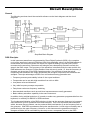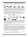
1
MAINTENANCE MANUAL
Model 29
10 MHz DDS
Function Generator
© 1997 Wavetek Ltd
This document contains information proprietary to
Wavetek and is provided solely for instrument
operation and maintenance. The information in this
document may not be duplicated in any manner
without the prior approval in writing from Wavetek.
Wavetek Ltd
Test and Measurement Division
Hurricane Way
Norwich Airport Industrial Estate
Norwich, Norfolk NR6 6JB, U.K.
Tel: 44 1603 256 600
Fax: 44 1603 483 670
Manual Issue: 1.1
Manual Part Number:
Table of Contents
Specifications
2
Safety
6
EMC
7
Installation
7
General
9
Circuit Descriptions
10
Calibration
15
Parts List
18
Circuit Diagrams
25
1
Specifications
Specifications apply at 18°-28°C after one hour warm-up, at maximum output into 50Ω
WAVEFORMS
STANDARD
Sine, square, positive pulse, negative pulse, multi-level squarewave, triangle, ramp up, ramp
down, DC and pseudo-random noise.
ARBITRARY
Sampling Frequency:
Waveform Length::
Vertical Resolution:
27.48MHz
1024 points maximum
10 bits
FREQUENCY
Frequency ranges for standard waveform are listed below. In Arbitrary mode all waveform points
are output up to approximately 27 kHz beyond which they are sampled.
Sine:
Square:
Positive/Negative Pulse:
Triangle:
Positive/Negative Ramp:
Multi-level square:
Pseudo-random noise:
Resolution:
Accuracy:
Stability:
100 µHz to 10 MHz
100 µHz to 10 MHz
100 µHz to 10 MHz
100 µHz to 100 kHz
100 µHz to 100 kHz
100 µHz to 100 kHz
30 mHz to 700 kHz
7 digits (limited by 100 µHz)
Typically 10 ppm for 1 year, 18°C to 28°C
Typically 1ppm per °C outside 18°C to 28°C
WAVEFORM CHARACTERISTICS
Sine Distortion:
Non-harmonic spurs:
Square Rise/Fall Time:
Square Aberrations:
Square Symmetry Control:
Triangle Linearity Error:
Triangle Symmetry Control:
Pulse Rise/Fall Time:
Pulse Aberrations:
Pulse Symmetry Control:
Multi-level Square:
2
<0.3% to 500 kHz
<-50 dBc to 1 MHz
<-35 dB to 10 MHz
typically -50 dBc to 10 MHz
<25 ns
<5% + 2 mV
1 to 99% (0.1% resolution) 100 µHz to 30 kHz
20 to 80% (0.1% resolution) 30 kHz to 10 MHz
<0.5% to 30 kHz
1 to 99% (0.1% resolution) 100 µHz to 100 kHz
<25 ns
<5% + 2 mV
1 to 99% (0.1% resolution) 100 µHz to 30 kHz
20 to 80% (0.1% resolution) 30 kHz to 10 MHz
Maximum of 16 steps of discrete amplitude and duration (1 to 1,024
points). Allows generating 3 level square, staircase, multiplexed
LCD driver signals, etc.
OUTPUT CHARACTERISTICS
Output Impedance:
Amplitude:
DC Offset:
Resolution:
Accuracy:
Flatness:
50Ω or 600Ω switchable
2.5 mVpp to 10 Vpp into 50Ω/600Ω
5 mVpp to 20 Vpp into open circuit
±5V (limited by offset plus signal peak) into 50Ω/600Ω
±10V (limited by offset plus signal peak) into open circuit
3 digits (limited by 1 mV)
3% + 1 mV at 1 kHz into 50Ω/600Ω
±0.2 dB to 500 kHz, ±1 dB to 5 MHz, ±2.5 dB to 10 MHz
OPERATING MODES
CONTINUOUS
Continuous cycles of the selected waveform are output at the programmed frequency.
TRIGGER/BURST
Phase coherent triggering of the programmed number of cycles of the selected waveform.
Waveforms start and stop at the phase angle specified in the Start/Stop phase parameter.
Trigger Sources:
Burst Count:
Trigger Repetition Rate:
External signal, manual (front panel key), internal trigger generator or
remote command.
1 to 1023 cycles
dc to 50 kHz (internal trigger generator)
dc to 1 MHz (external trigger signal)
GATE
Cycles of the selected waveform are continuously output while the trigger signal is present.
Trigger Sources:
Trigger Repetition Rate:
External signal, manual (front panel key), internal trigger generator or
remote command
dc to 50 kHz (internal trigger generator)
dc to 1 MHz (external trigger signal)
SWEEP
Sweep Mode:
Frequency Range:
Markers:
Trigger Sources:
Linear or logarithmic, single triggered cycle or continuous
100 µHz to the maximum frequency for selected waveform
Two variable markers during sweep
External signal, manual (front panel key), or remote command
FREQUENCY HOP
Up to 16 different hop waveforms, each with independently setable frequency, amplitude, offset,
waveform (except noise), and duration for each waveform. Phase continuous switching between
frequencies can be executed via software or manually (front panel key). Waveform duration can
be set from 2 ms to 65 s in 1 ms increments. HOP can be externally triggered from the EXT TRIG
input.
3
AMPLITUDE MODULATION
Carrier Frequency Range 100 µHz to the maximum frequency for selected waveform.
Carrier Waveforms:
Depth:
Internal Source:
External Source:
External Sensitivity:
All
Typically variable from 0% to 100% in 1% increments
1 kHz fixed sinewave or 5 mHz to 50 kHz squarewave
DC to 100 kHz (4 quadrant)
Approximately 2 Vpp for 50% modulation
FREQUENCY SHIFT KEYING (FSK)
Phase coherent switching between two selected frequencies at a rate defined by the switching
signal source.
Carrier Frequency:
Carrier Waveforms:
Switch Repetition Rate:
Switching Signal Source:
100 µHz to the maximum frequency for selected waveform
All
dc to 50 kHz (internal trigger generator)
dc to 1 MHz (external trigger signal)
Internal from front panel key or internal trigger generator
External from Trig/Gate input or remote interface
START/STOP PHASE
Phase relationship between MAIN OUT and AUX OUT is determined by the START/STOP
PHASE setting.
Carrier Frequency:
Carrier Waveforms:
Range:
Resolution:
100 µHz to 1 MHz
All
0 to 360 degrees
1 degree
TRIGGER GENERATOR
Internal source 5 mHz to 50 kHz squarewave adjustable in 20 µs steps with 3 digit resolution.
Available for output at the sweep/marker connector (except during sweep or HOP operation).
OUTPUTS/INPUTS
FRONT PANEL CONNECTIONS
MAIN OUT
AUX OUT:
EXT TRIG:
4
Waveform output at 50Ω or 600Ω (selectable) impedance.
Short circuit protection for up to 60 seconds is provided.
CMOS/TTL level signal at the frequency and symmetry of main output.
Phase relationship between MAIN OUT and AUX OUT is determined
by the START/STOP PHASE setting.
External trigger input for Trigger, Gate, Sweep and FSK operating
modes. It is also used to synchronize one Model 29 (as a slave) to
another Model 29 (as a master).
Maximum input voltage is ±10V.
REAR PANEL CONNECTIONS
CLOCK IN/OUT
CLOCK IN
CLOCK OUT
PHASE LOCK
VCA IN
SYNC OUT
TRIG/SWEEP OUT
The function of the CLOCK IN/OUT connector is set from the front
panel SYS (system) menu as follows:
The connector serves as an input for an external clock
This is the default setting. The internal clock is made available as an
output. When two or more Model 29s are synchronized the CLOCK
OUT is used as a master to drive the CLOCK IN of the slave units.
For use as a slave unit phase locked to the master unit.
Input connector for externally controlled Amplitude Modulation (AM).
Impedance is nominally 6 kΩ.
When two or more generators are syncronized the SYNC OUT
connector on the master generator is connected to the EXT TRIG
inputs of the slave generators. SYNC OUT logic levels are nominally
0V and 5V with 50Ω output impedance.
The function of this output is automatically determined by the generator
operating mode. Except in sweep and HOP modes the output is that of
the internal trigger generator, a fixed amplitude squarewave whose
frequency is set in the TRIG of GATE menus. The rising edge of the
trigger generator initiate trigger, gate and burst modes. In sweep mode
the output is a 3-level waveform, changing from high (4V) to low (0V) at
the start of the sweep, with narrow 1V pulses at marker points. In HOP
mode the output goes low on entry to each waveform step and high
after the new frequency and waveshape of that step have been set.
Output impedance is 1kΩ.
INTERFACES
Full remote control facilities are provided through RS232 and IEEE-488 (GPIB) interfaces.
RS232:
IEEE-488:
Variable baud rate, 9600 baud max;, 9-pin D connector.
Conforms with IEEE-488.1 and IEEE.488.2
STORED SETTINGS
Up to 9 complete instrument set-ups may be stored and recalled from battery backed memory.
GENERAL
Display:
Size:
Weight:
Power
Operating Range:
Storage Range:
Options:
Safety:
EMC:
20 character by 4 row alphanumeric display.
130 mm (height), 212 mm (width), 330 mm (depth)
9 pounds (4.1 kg)
115 V or 230 V nominal 50/60 Hz, adjustable internally,
operating range ±14% of nominal, 30 VA maximum.
5°C to 40°C, 20-80%RH
-20°C to 60°C
19” Rack Mount Kit
Complies with EN61010-1
Complies with EN55011 and EN50082-1.
5
Safety
This function generator is a Safety Class I instrument according to IEC classification and has
been designed to meet the requirements of EN61010-1 (Safety Requirements for Electrical
Equipment for Measurement, Control and Laboratory Use). It is an Installation Category II
instrument intended for operation from a normal single phase supply.
This instrument has been tested in accordance with EN61010-1 and has been supplied in a safe
condition. This service manual contains some information and warnings which have to be
followed by the user to ensure safe operation and to retain the instrument in a safe condition.
This instrument has been designed for indoor use in a Pollution Degree 1 environment (no
pollution, or only dry non-conductive pollution) in the temperature range 5°C to 40°C, 20% - 80%
RH (non-condensing). It may occasionally be subjected to temperatures between +5° and -10°C
without degradation of its safety.
Use of this instrument in a manner not specified by these instructions may impair the safety
protection provided. Do not operate the instrument outside its rated supply voltages or
environmental range. In particular excessive moisture may impair safety.
WARNING! THIS INSTRUMENT MUST BE EARTHED
Any interruption of the mains earth conductor inside or outside the instrument will make the
instrument dangerous. Intentional interruption is prohibited. The protective action must not be
negated by the use of an extension cord without a protective conductor.
When the instrument is connected to its supply, terminals may be live and opening the covers or
removal of parts (except those to which access can be gained by hand) is likely to expose live
parts. The apparatus shall be disconnected from all voltage sources before it is opened for any
adjustment, replacement, maintenance or repair.
Any adjustment, maintenance and repair of the opened instrument under voltage shall be avoided
as far as possible and, if inevitable, shall be carried out only by a skilled person who is aware of
the hazard involved.
If the instrument is clearly defective, has been subject to mechanical damage, excessive moisture
or chemical corrosion the safety protection may be impaired and the apparatus should be
withdrawn from use and returned for checking and repair.
Make sure that only fuses with the required rated current and of the specified type are used for
replacement. The use of makeshift fuses and the short-circuiting of fuse holders is prohibited.
This instrument uses a Lithium button cell for non-volatile memory battery back-up; typical life is 5
years. In the event of replacement becoming necessary, replace only with a cell of the correct
type, i.e. 3V Li/Mn02 20mm button cell type 2032. Exhausted cells must be disposed of carefully
in accordance with local regulations; do not cut open, incinerate, expose to temperatures above
60°C or attempt to recharge.
Do not wet the instrument when cleaning it and in particular use only a soft dry cloth to clean the
LCD window. The following symbols are used on the instrument and in this manual:Caution - refer to the accompanying documentation, incorrect
operation may damage the instrument.
terminal connected to chassis ground.
mains supply OFF.
l
mains supply ON.
alternating current.
6
EMC
This function generator has been designed to meet the requirements of the EMC Directive
89/336/EEC.
Compliance was demonstrated by meeting the test limits of the following standards:
Emissions
EN55011 (1991) for industrial, scientific and medical (ISM) radio-frequency equipment;
Group 1 Class B limits were applied.
Immunity
EN50082-1 (1992) Generic immunity standard for residential, commercial and light
industry. Test methods and limits used were:
a) EN60801-2 (1993) Electrostatic Discharge, 8 kV air discharge.
b) IEC801-3 (1984) RF Field, 3 V/m.
c) IEC801-4 (1988) Fast Transient, 1 kV peak.
Cautions
To ensure continued compliance with the EMC directive the following precautions should be
observed:
a) connect the generator to other equipment using only high quality, double-screened cables.
b) after opening the case for any reason ensure that all signal and ground connections are
remade correctly before replacing the cover. Always ensure all case screws are correctly
refitted and tightened.
c) In the event of part replacement becoming necessary, only use components of an identical
type, see the Parts List.
Installation
Check that the instrument operating voltage marked on the rear panel is suitable for the local
supply. Should it be necessary to change the operating voltage, proceed as follows:
1) Disconnect the instrument from all voltage sources.
2) Remove the screws which retain the top cover and lift off the cover.
3) Change the transformer connections as follows:
for 230V operation connect the live (brown) wire to pin 15
for 115V operation connect the live (brown) wire to pin 14
for 100V operation connect the live (brown) wire to pin 13.
4) Refit the cover and the secure with the same screws.
5) To comply with safety standard requirements the operating voltage marked on the rear panel
must be changed to clearly show the new voltage setting.
6) Change the fuse to one of the correct rating, see below.
7
Fuse
Ensure that the correct mains fuse is fitted for the set operating voltage. The correct mains fuse
types are:
for 230V operation:
250 mA (T) 250 V HRC
for 110V/115V operation:
500 mA (T) 250 V HRC
To replace the fuse, disconnect the mains lead from the inlet socket and release the fuse drawer
below the socket pins by depressing both clips together, with miniature screwdrivers, so that the
drawer can be eased open. Change the fuse and replace the drawer.
The use of makeshift fuses or the short-circuiting of the fuse holder is prohibited.
Mains Lead
When a three core mains lead with bare ends is provided it should be connected as follows:Brown Mains Live
Blue Mains Neutral
Green / Yellow Mains Earth
WARNING! THIS INSTRUMENT MUST BE EARTHED
Any interruption of the mains earth conductor inside or outside the instrument will make the
instrument dangerous. Intentional interruption is prohibited. The protective action must not be
negated by the use of an extension cord without a protective conductor.
Mounting
This instrument is suitable both for bench use and rack mounting. It is delivered with feet for
bench mounting. The front feet include a tilt mechanism for optimal panel angle.
A rack kit for mounting one or two of these Half-width 3U high units in a 19” rack is available from
the Manufacturers or their overseas agents.
8
General
Service Handling Precautions
Service work or calibration should only be carried out by skilled engineers. Please note the
following points before commencing work.
Most of the integrated circuits are CMOS devices and care should be taken when handling to
avoid damage by static discharge.
Many of the devices are miniature surface mount components with very fine leads on small
pitches; these components must be removed and replaced with great care to avoid damage to
the pcb. It is essential that only tools and soldering equipment specifically designed for surface
mount components are used.
The decoupling capacitors associated with the integrated circuits are surface mounted on the
solder side of the pcb.
Dismantling the Instrument
WARNING
Disconnect the instrument from all voltage sources before it is opened for adjustment or repair. If
any adjustment or repair of the opened instrument is inevitable it shall be carried out only by a
skilled person who is aware of the hazards involved.
1.
Remove the six screws retaining the top cover.
2.
The rear panel may be removed as follows. Disconnect the gray ribbon cable from PJ4
on the GPIB pcb and remove the 2 screwjacks which secure the RS232 connector to the
rear panel. Invert the instrument and remove the three screws securing the rear panel;
the panel may now be tilted back to allow access. If the panel is to be completely
removed unplug connectors from PJ4, PJ7 & PJ8 and the blue and brown wires from the
mains inlet filter; desolder the blue and brown wires from the mains transformer. The
panel can now be lifted free of the instrument.
3.
The front panel assembly may be removed as follows. Unplug the connectors from PJ2,
PJ3, PJ5 & PJ6 and desolder the screened cable from PJ10. Remove the nut securing
the front panel earthing strap and the four nuts securing the front panel assembly. The
panel may now be drawn clear of the instrument.
4.
Main pcb removal. Remove all connectors from the pcb and desolder the screened cable
from PJ10. Tilt the rear panel back as described in 2 above. Remove the pcb fixing screw
nearest PJ10; invert the instrument and remove the 5 screws retaining the pcb fixing
pillars to the case lower. The main pcb can now be lifted free, complete with its fixing
pillars.
5.
When re-assembling the instrument ensure that the correct fastenings are used.
9
Circuit Descriptions
General
The following sections should be read with reference to the block diagram and the circuit
diagrams.
Simplified Block Diagram
DDS Principles
In this instrument waveforms are generated by Direct Digital Synthesis (DDS). One complete
cycle of the waveform is stored in RAM as 1024 10-bit amplitude values. As the RAM address is
incremented, the waveform values are output to a Digital-to-Analog Converter (DAC) which
reconstructs the waveform. Sinewaves and triangles are subsequently filtered to smooth the
steps in the DAC output. The frequency of the waveform is determined by the rate at which the
RAM addresses are changed. Further details of how this rate is varied, i.e. how the frequency is
changed, are given later in the DDS Operation section; it is sufficient to know that at low
frequencies the addresses are output sequentially but at higher frequencies the addresses are
sampled. The major advantages of DDS over conventional analog generation are:
•
Frequency accuracy and stability is that of the crystal oscillator.
• Frequencies can be set with high resolution from mHz to MHz.
• Low phase noise and distortion.
• Very wide frequency sweeps are possible.
• Fast phase continuous frequency switching.
• Non-standard waveforms such as multi-level squarewaves are easily generated.
• Basic arbitrary waveform capability in the same instrument.
In addition, being a digital technique, it is easier to make every parameter programmable from the
keyboard, or remotely via RS232 or GPIB interfaces.
The fundamental limitation of the DDS technique is that, as the generator frequency is increased,
each waveform cycle is constituted from fewer samples. This is not a problem with sinewaves
which, because they are filtered, can be produced with low distortion up to the frequency limit of
the generator. With DDS squarewaves and pulse waveforms the 1 clock edge uncertainty sets a
practical limit to the upper frequency. However, on this instrument the generation technique
changes at 30kHz (but is overridable by the user) to use a comparator driven by the DDS
10
sinewave; this ensures jitter-free squarewaves and pulses up to the frequency limit of the
generator. Ramp and staircase waveforms are by default, unfiltered (although filtering can be
selected) and therefore become degraded above the frequencies indicated in the Specification;
all waveforms are, however, available up to the maximum frequency of the generator.
DDS Operation
One complete cycle of the selected waveform is stored in RAM as 1024 10-bit amplitude values.
As the RAM address is incremented the waveform values are output sequentially to a Digital-toAnalog Converter (DAC) which reconstructs the waveform as a series of voltage steps.
Sinewaves and triangles are subsequently filtered to smooth the steps in the DAC output.
The frequency of the output waveform is determined by the rate at which the RAM addresses are
changed; in a DDS system the address changes are generated as follows.
The RAM contains the amplitude values of all the individual points of 1 cycle (360°) of the
waveform; each sequential address change corresponds to a phase increment of the waveform of
360°/1024. Instead of using a counter to generate sequential RAM addresses, a phase
accumulator is used to increment the phase.
On each clock cycle the phase increment, which has been loaded into the phase increment
register by the CPU, is added to the current result in the phase accumulator; the 10 most
significant bits of the phase accumulator drive the RAM address lines. The output waveform
frequency is now determined by the size of the phase increment at each clock. If each increment
is the same size then the output frequency is constant; if it changes, the output frequency
changes but with phase continuity.
The generator uses a 38-bit accumulator and a clock frequency which is 238 x 10-4
(~27.487MHz); this yields a frequency resolution (corresponding to the smallest phase increment)
of fCLK/238 = 0.1mHz.
Only the 10 most significant bits of the phase accumulator are used to address the RAM. At a
waveform frequency of fCLK/1024 (~26.84kHz), the ‘natural’ frequency, the RAM address
increments on every clock. At all frequencies below this (i.e. at smaller phase increments) one or
more addresses are output for more than one clock period because the phase increment is not
big enough to step the address at every clock. Similarly at waveform frequencies above the
natural frequency the larger phase increment causes some addresses to be skipped, giving the
effect of the stored waveform being ‘sampled’; different points will be sampled on successive
cycles of the waveform. The minimum number of points required to accurately reproduce a
waveshape will determine the maximum useful output frequency:
fmax = fCLK/No. of points
For sinewaves the filter permits the waveform to be reproduced accurately up to the Nyquist limit
(fCLK/2), although in this generator a practical limit of 10MHz is set.
11
MPU and Memory
The majority of the digital hardware in the instrument is contained in 3 LSI devices, these being a
MicroProcessor Unit, IC36, and 2 Field Programmable Gate Arrays, IC41 and IC44.
The Z80180 MPU contains an 8 bit Z80 core, 2x16 bit counter-timers, 2x8 bit serial interfaces and
a memory management unit. The MPU is clocked at 12MHz by XTL1.
The MPU provides up to 20 memory address lines but only the lower 18 are used to provide
access to 256k bytes of memory This comprising a 256k byte EPROM, IC38, with the top 32k
bytes overlaid by SRAM, IC39. The MPU selects between the memory devices via a decoder
located in the FPGA at IC44.
The RS232 interface is provided directly by the MPU and is buffered to the rear panel connector,
PJ1, by IC34 and IC35.
One of the counter-timers provides a constant 125us 'tick' to the MPU which is used to time all
the housekeeping functions, e.g. keyboard scan, knob control, as well as some generator
functions, e.g. frequency sweep. The second counter-timer is used by the Trigger generator.
Keyboard, LCD and Leds
The keyboard is interrogated every 10ms. This is done by reading the registers in IC19 and IC45.
If a key is down then one of the transistors Q15-Q20 will be on and the corresponding bits read
from IC19/IC45 will be high. The MPU decodes this to produce a key code which is passed to the
software. Multiple keys down are ignored. IC44 provides the port decode signals for access to
IC19 and IC45.
The knob is connected directly to the FPGA, IC44. This decodes the 4 states of the switches and
increments/decrements a counter. The counter is read and cleared every 10ms and the value and
sign passed to the software.
The 16 leds are driven directly from the latches in the shift registers IC14 and IC15. These
latches are updated as required via the FPGA, IC44.
The LCD is accessed via a bi-directional 4 bit port in IC44
GPIB
The FPGA, IC44, provides the port select signals to the GPIB board if fitted. The software
automatically detects the presence of the GPIB board at power up and allows the user to select it
on the REMOTE menu.
DDS FPGA
The FPGA, IC41, provides the complete DDS system including 38-bit phase accumulator, two 38bit registers to hold the frequency values for FSK, trigger/gate control logic, 10-bit re-loadable
burst counter, multi-instrument phase synchronization logic and an 8-bit 16-port bi-directional
MPU interface. Access is provided to the waveform RAM to allow the patterns to be written and
the AUX output signal is generated or selected.
All internal operations of the FPGA are clocked by the signal DDSCLK. Note that if this signal is
interrupted it is possible for the FPGA to become non-functional requiring that the FPGA be
completely reset. The clock could be interrupted by a fault condition or by setting the CLOCK
BNC to INPUT and then providing an unacceptable clock. An unacceptable clock is any signal
which overrides the internal clock but produces a replacement which is less than 5MHz or greater
than 27.5MHz; one way to accidentally accomplish this is to connect a 50Ω pad across the clock
input.
Pseudo random noise may also be generated by the FPGA. Each time the user turns noise ON or
OFF the FPGA is re-programmed to the required function. Note that this also has the effect of
completely resetting the FPGA.
12
Trigger Generator
This is created from the second counter-timer in the MPU and a programmable divide by
1/10/100/1000 counter in the FPGA, IC44. The counter-timer produces a squarewave in the
range 50kHz to 5Hz and the divider extends this to 0.005Hz.
Waveform DAC and filter
IC1 is a high speed 10-bit DAC whose data is latched on the rising edge of the clock. The DAC
output is 1Vp-p and is referred to the +5VA rail. IC1 has an internal 2V reference at pin 16
referred to +5VA.
L3, L4, L5 and associated components form a 7-stage elliptic filter with sinx/x correction. The
inductors L3,L4 and L5 are factory preset before manufacture and must not be adjusted. Relay
RL1 allows the filter to be switched in and out.
Amplifier and Level Shift
IC7 is a current feedback amplifier. The output of IC7 is approximately 4Vp-p and is centered
around 0VA. IC11C selects the waveform source and IC11A selects low pass filter R3/C17 when
in noise mode.
High Frequency Squarewaves
Low frequency squarewaves are generated via the RAM and DAC, high frequency squarewaves
are generated by converting the sinewave to square with comparator IC6. Adjusting the
comparator threshold varies high frequency symmetry. The comparator output drives IC4 which
gives squarewaves above, below or about 0VA.
Amplitude Control and Modulation
IC2 is a 4-quadrant multiplier. Amplitude is voltage controlled via IC8A. AM is selected by IC11B
and IC25C. The internal squarewave modulation source is generated by IC25B; the amplitude is
adjusted by varying the levels that IC25B switches between. The internal sinewave modulation
source is fixed at 1kHz and is achieved by passing the output of IC25B through a Sallen and Key
low pass filter. The current output of IC2 is converted to a voltage by R44 giving approximately
900mVp-p at maximum output. IC46 amplifies this to give approximately 3.6Vp-p.
Output Amplifier and Attenuators
IC3 is an intermediate switched attenuator giving 0dB, -12dB and -20dB. IC10 is a current
feedback amplifier with a gain of approximately 5.5 and gives 20Vp-p at maximum output. DC
offset control is via R33 and IC8B. Relays RL2 and RL3 select -20dB 50Ω attenuators. Relay RL4
selects 50 or 600 Ω output impedance and RL5 output on/off.
DAC and Sample and Holds
IC18 is a 12-bit serial DAC with internal 2V reference. IC31 provides a bipolar output. IC20
multiplexes the DAC output voltage onto the appropriate hold capacitor. FET input amplifiers IC12
and IC24 buffer the voltages on the hold capacitors. The voltage at each sample and hold is
controlled by the MCU which calculates each value from a combination of the instrument set up
and the calibration constants stored in EEPROM.
13
Power Supply
The transformer has two separate secondaries, one for the digital supply the other for the analog
supplies. The digital 5V is supplied by low drop-out regulator IC27. The display backlight current
is sourced from the unregulated side of IC27. The backlight current is controlled by a 200mA
current source Q8/IC26A. IC28 and IC29 provide the analog +/-15V rails and IC30 the -5V. IC5
provides local regulation for the waveform DAC IC1. Digital and analog grounds join at the
waveform DAC IC1. PJ11 is a test point for the supply rails. Three PCB mounted fuses protect
the transformer secondaries under fault conditions.
Required values measured at PJ11:
pin 1: +15V +/-0.6V
pin 5: -15V +/-0.6V
pin 2: +5VA +/-0.2V
pin 6: +5VCPU +/-0.2V
pin 4: -5VA +/-0.2V
14
Calibration
All parameters can be calibrated without opening the case, i.e. the generator offers ‘closed-box’
calibration. All adjustments are made digitally with calibration constants stored in EEPROM. The
calibration routine requires only a DVM and a frequency counter and takes no more than a few
minutes.
The crystal in the timebase is pre-aged but a further aging of up to ± 5ppm can occur in the first
year. Since the aging rate decreases exponentially with time it is an advantage to recalibrate after
the first 6 month’s use. Apart from this it is unlikely that any other parameters will need
adjustment.
Calibration should be carried out only after the generator has been operating for at least an hour
in normal ambient conditions.
Equipment Required
• 3½ digit DVM with 0.25% DC accuracy and 0.5% AC accuracy at 1kHz.
• Frequency counter capable of measuring 10.00000MHz and 50µs ±0.1µs pulsewidths.
The DVM is connected to the MAIN OUT and the counter to the AUX OUT.
Frequency meter accuracy will determine the accuracy of the generator’s clock setting and
should ideally be ±1ppm.
It may be quicker to use an oscilloscope for steps 05 and 15 (see next section).
Calibration Procedure
The CALibration procedure is accessed by pressing the blue EDIT key followed by CAL, the
shifted function of 6. At each step the display changes to prompt the user to adjust the rotary
control or FIELD/DIGIT keys, until the reading on the specified instrument is at the value given.
The FIELD keys provide very coarse adjustment, the DIGIT keys coarse adjustment and the
rotary control fine adjustment. Pressing ENTER increments the procedure to the next step;
pressing CE decrements back to the previous step. Alternatively, pressing ESCAPE exits to the
last CAL display at which the user can choose to either keep the new calibration values (ENTER),
return to the old values (ESCAPE) or restart the calibration procedure (CE).
The first two displays (CAL 00 and CAL 01) specify the connections and adjustment method. The
subsequent displays, CAL 02 to CAL 20, permit all adjustable parameters to be calibrated.
The full procedure is listed below; the name of the control signal being adjusted at each step and
the default DAC value are shown in brackets. The display itself shows a summary of the step
adjustment procedure and the actual DAC value.
CAL 02
Output DC offset zero; adjust for 0V ± 5mV (DCOFFSET, 2060).
CAL 03
Output DC offset +ve full scale; adjust for 10V ± 20mV (DCOFFSET, 4000).
CAL 04
Output DC offset -ve full scale; check for -10V ± 20mV (DCOFFSET, 0120).
CAL 05
Multiplier control zero offset; adjust for minimum output (AMPL, 2060).
CAL 06
HF squarewave, IC4 grounded; note offset.
CAL 07
Waveform DAC at mid-scale; adjust for CAL06 value ± 10mV (WAVOFST, 1820).
CAL 08
Waveform DC offset; adjust for 0V ± 5mV (DCOFFSET, 2058).
CAL 09
Waveform DAC at full scale; adjust for 10V ± 10mV (AMPL, 0300).
CAL 10
HF squarewave full scale; adjust for 10V ± 10mV (SQLEVEL, 1100).
CAL 11
–20dB output attenuator; adjust for 1V ± 1mV (AMPL, 4000).
15
CAL 12
–40dB output attenuator; adjust for 0.1V ± 0.1mV (AMPL, 4000).
CAL 13
–12dB intermediate attenuator; adjust for 1.768VAC ± 5mV (AMPL, 0300).
CAL 14
–20dB intermediate attenuator; adjust for 0.707VAC ± 1mV (AMPL, 0300).
CAL 15
AM squarewave zero; adjust for minimum output, (+AMSQ, 2050).
CAL 16
AM squarewave full scale; adjust for 10V ± 10mV (+AMSQ, 1000).
CAL 17
AM sinewave full scale; adjust for 3.54VAC ± 10mV (+AMSQ, 0650).
Check for a good sinewave on the scope.
CAL 18
HF squarewave symmetry (50%); adjust for 50us ± 0.1us (SYM, 2060).
CAL 19
HF squarewave symmetry (75%); adjust for 75us ± 0.1us (SYM, 2741).
CAL 20
Clock calibrate. 10MHz at main and aux outputs or 27.48779MHz at clock in/out
when set as an output; adjust to ±1ppm. Fail if outside these limits. 300-3700
shown on the display (2000).
Press ENTER twice to store new values and exit calibration mode.
Each adjustment step allows the MCU to calculate a calibration constant which is stored in
EEPROM. Because each step allows a very wide adjustment range it is possible to stop the
instrument functioning completely; if this is suspected the default values listed above should be
set and a complete recalibration should then be performed.
When CAL is first entered and the confirmation screen is displayed, pressing the CE key will
invoke a set of hardware tests. Follow the on-screen prompts to execute these tests. Note: The
RAM test will not function correctly if SWEEP is active when CAL is entered.
CALIBRATION PASSWORD
V1.6 and later firmware provides for a 4-digit password in the range 0000 to 9999 to be used to
access the calibration procedure. If the password is left at the factory default of 0000 no
messages are shown and calibration is accessed exactly as described in the Calibration section;
only if a non-zero password has been set will the user be prompted to enter the password.
Setting the Password
Press the blue EDIT key followed by CAL (the shifted function of 6) to show the opening screen of
the calibration routine. With this screen displayed press EDIT again to show the password
screen:
ENTER NEW PASSWORD
---Enter a 4-digit password from the keyboard; the display will show the message NEW
PASSWORD STORED! for two seconds and then revert to the Main menu. If any keys other than
0-9 are pressed while entering the password the message INCORRECT PASSWORD! will be
shown.
16
Using the Password to Access Calibration or Change the Password
With the password set, pressing EDIT following by CAL will now change the screen to:
ENTER PASSWORD
---When the correct password has been entered from the keyboard the display changes to the
opening screen of the calibration routine and calibration can proceed as described in the
Calibration section. If an incorrect password is entered the message INCORRECT PASSWORD!
is shown for two seconds before the display reverts to the Main menu.
With the opening screen of the calibration routine displayed after correctly entering the password,
the password can be changed by pressing the EDIT key and following the procedure described in
Setting the Password. If the password is set to 0000 again, password protection is removed.
The password is held in EEPROM and will not be lost when the memory battery back-up is lost.
In the event of the password being forgotten, contact the manufacturer for help in resetting the
instrument.
17
Parts List
PCB ASSY MAIN - (44912-0270)
Part Number
Description
Position
20234-0011
SCREW M3 X 10 PNHDPZ NPST
FOR PJ1
20613-9401
WASHER TO220 ADHESIVE
FOR SK1-4
20670-0130
HEATSINK PCB MTG 25MM HIGH
SK1
20670-0135
CLIP GP02 FOR PCB MTG H/SINKS
FOR SK1-4
20670-0200
HEATSINK PCB MTG 50MM HIGH
SK2,3,4
20670-0340
T0220 CLIP ON HEATSINK 29DEG/W
FOR Q8
22010-0610
BATTERY 3V LITH 20MM BUTTON
BATT
22040-0920
BEAD FERRITE LEADED
FB1-6
22042-0181
INDUCTOR 4.3UH
L5
22042-0182
INDUCTOR 4.8UH
L4
22042-0183
INDUCTOR 5.0UH
L3
22160-0002
CHOKE 1 AMP VHF SUPP
L1
22240-0020
RELAY TYPE 53/5 (24V)
RL1,2,3
22240-0050
RELAY TYPE 47 (24V)
RL4,5
22315-0450
FUSE 500Mat SUBMIN PCB MNT
FS1,3
22315-0453
FUSE 1.5AT SUBMIN PCB MNT
FS2
22469-0203
VERO PIN 18-0223K
FOR PJ10
22573-0041
HEADER 2 WAY STRAIGHT
LK1,2
22573-0202
HEADER 2 WAY STRAIGHT .156P
PJ5,8,9
22573-0205
HEADER 5 WAY STRAIGHT .156P
PJ7
22573-0206
HEADER 6 WAY STRAIGHT .156P
PJ4
22574-0400
SKT 9W R/A D-TYPE (RS232)
PJ1
22575-0009
SHORTING BLOCK RED
FOR BATTERY
22575-0038
HEADER 6 WAY STR 0.1P
PJ11
22575-0065
HEADER 20 WAY (2X10) STR SKELN
PJ6
22575-0066
HEADER 40 WAY (2X20) STR SKELN
PJ2
22575-0100
HEADER 34 WAY (2X17) STR SKELN
PJ3
23185-0000
RES ZERO OHM
R58
23202-0100
RES 10R0F W25 MF 50PPM
R121,147
23202-0102
RES 10R2F W25 MF 50PPM
R53,56
23202-0360
RES 36R0F W25 MF 50PPM
R37,40,185
23202-0470
RES 47R0F W25 MF 50PPM
R23,32
23202-0560
RES 56R0F W25 MF 50PPM
R39
23202-0680
RES 68R0F W25 MF 50PPM
R36
18
PCB ASSY MAIN – (44912-0270) continued/…
Part Number
Description
Position
23202-1100
RES 100RF W25 MF 50PPM
R2,22,24,45,46,81,82,103,165,167,186
23202-1120
RES 120RF W25 MF 50PPM
R85,86,87,88,90,91,97,98,99,159
23202-1150
RES 150RF W25 MF 50PPM
R67
23202-1191
RES 191RF W25 MF 50PPM
R176
23202-1220
RES 220RF W25 MF 50PPM
R3,113
23202-1270
RES 270RF W25 MF 50PPM
R38,168,169,170
23202-1330
RES 330RF W25 MF 50PPM
R16,62
23202-1360
RES 360RF W25 MF 50PPM
R149
23202-1470
RES 470RF W25 MF 50PPM
R44,63,65
23202-1510
RES 510RF W25 MF 50PPM
R31,33
23202-1549
RES 549RF W25 MF 50PPM
R57
23202-1680
RES 680RF W25 MF 50PPM
R21,71,77,89,93,134-140,175
23202-1750
RES 750RF W25 MF 50PPM
R15
23202-2100
RES 1K00F W25 MF 50PPM
R4-13,61,83,120,152,153,156-158,
163,173,174
23202-2137
RES 1K37F W25 MF 50PPM
R142
23202-2150
RES 1K50F W25 MF 50PPM
R66
23202-2200
RES 2K00F W25 MF 50PPM
R68,164
23202-2270
RES 2K70F W25 MF 50PPM
R184
23202-2330
RES 3K30F W25 MF 50PPM
R35,116,179
23202-2470
RES 4K70F W25 MF 50PPM
R34,70,72,73,74,75,154,155,162, 166,172,
177,178
23202-2820
RES 8K20F W25 MF 50PPM
R60
23202-2910
RES 9K10F W25 MF 50PPM
R59, 130
23202-3100
RES 10K0F W25 MF 50PPM
R80,84,101,102,106-109,111,112,
114,115,123,124,127,129,143,180,181
23202-3120
RES 12K0F W25 MF 50PPM
R17,20,25,27,28
23202-3180
RES 18K0F W25 MF 50PPM
R148
23202-3200
RES 20K0F W25 MF 50PPM
R132,160,161,171
23202-3270
RES 27K0F W25 MF 50PPM
R144,150
23202-3330
RES 33K0F W25 MF 50PPM
R151
23202-3430
RES 43K0F W25 MF 50PPM
R133
23202-3470
RES 47K0F W25 MF 50PPM
R117,118,146
23202-4100
RES 100KF W25 MF 50PPM
R14,92,104,110,125
23202-5100
RES 1M00F W25 MF 50PPM
R105
23206-0033
RES 3R3F W60 MF 100PPM MRS25
R141
23206-0412
RES 41R2F W60 MF 50PPM MRS25
R51,52,54,55
23206-1200
RES 200RF W60 MF 50PPM MRS25
R47,48,49,50
19
PCB ASSY MAIN - (44912-0270) continued/...
Part Number
Description
Position
23206-6100
RES 10M0F W60 MF 50PPM MRS25
R126,128
23222-0047
RES 4R7J W33 MF FUSIBLE NFR25
R29,30,76,95,96,145
23301-0435
RES NETWK SIL 1K0 X 5
RP1,2
23301-0443
RES NETWK SIL 22K X 8
RP3,4,5
23427-0268
CAP 22PG 100V CER NPO P2.5
C10,39,45-48,64,103,104
23427-0325
CAP 10NZ 63V CER HI K P5
C73-75,81-84,92-95,99,121,136,138
23427-0357
CAP 33PG 63V CER N150 P2.5
C21,32,101
23427-0374
CAP 100PG 100V CER N150 P2.5
C16,20,62
23427-0385
CAP 39PG 100V CER N150 P2.5
C22,90
23427-9205
CAP 47PG 100V CER NPO P2.5
C14,98,149
23427-9206
CAP 15PG 100V CER NPO P2.5
C63,91
23427-9210
CAP 3P3C 100V CER NPO P2.5
C38
23427-9218
CAP 330PK 100V CER MED K P2.5
C61
23427-9221
CAP 12PG 100V CER NPO P2.5
C15,18
23461-0020
CAP SM0805 100NZ 50V CER Y5V
SC1-37
23557-0530
CAP 100U 16V ELEC RC2 P2.5
C87
23557-0550
CAP 10U 16V ELEC BIPOLAR P2
C29,56,57,58,148
23557-0612
CAP 1U0 50V ELEC RE2 P2
C105
23557-0647
CAP 10U 35V ELEC RE2 P2
C1-9,33,34,78,79,80,89,119,120,135
23557-0664
CAP 1000U 35V ELEC RE2 P5
C76,77
23557-0673
CAP 22U 35V ELEC RE2 P2
C102
23557-9122
CAP 4700U 16V ELEC RE2 P7.5
C85
23620-0236
CAP 1N0K 100V P/E 435/1 P5
C17
23620-0242
CAP 22NJ 100V 5% P/E P5
C59
23620-0246
CAP 100NK 63V P/E P5
C11-13,24-28,35-37,41-44,49,52-54,60,
72,88,96,97,117,118,124,127,131,132,
134,137
23620-0249
CAP 330NK 63V P/E P5
C65-71,147
25021-0901
DIO 1N4148 B/R
D3,5,6,8-13,24-26
25061-0200
LED - T1 ROUND (3mm) - RED
LED1
25115-0907
DIO 1N4002 B/R
D14-21
25130-0903
DIO ZEN 5V1 W4
D1,2
25131-0224
DIO ZEN 18V 1W3
D22,23
25131-0226
DIO ZEN 6V2 1W3
D27
25174-0222
DIO VARICAP BB909B
D4
25336-5590
TRAN PNP BC559C
Q10,15-20
25341-0214
TRAN PNP ZTX214L/BC559
Q12
PCB Assy Main - (44912-0270) continued/...
20
Part Number
Description
Position
25380-0229
TRAN NPN BC549
Q3-7,11,13,14
25380-0230
TRAN NPN MPS2369
Q9
25386-9300
TRAN TIP31A
Q8
27103-0040
IC NE529N14 PIN
IC6
27106-0513
IC LM358N 8 PIN
IC26
27106-0517
IC NE5532N8 PIN
IC8
27106-0606
IC TL072CP8 PIN
IC31
27106-0628
IC TL074 14 PIN
IC9,12,24
27106-0633
IC EL2099CT 5 PIN TO-220
IC10
27106-0634
IC 2020 8 PIN
IC7,46
27151-1000
IC SM HA9P2557-9
IC2
27153-0080
IC LTC1257CN88 PIN
IC18
27153-0180
IC DAC MB4076020 PIN
IC1
27160-0009
IC V/REG 7805 TO220
IC5
27160-0012
IC V/REG 79L05 TO92
IC30
27160-0013
IC V/REG 7815 TO220
IC28
27160-0020
IC V/REG 7915 TO220
IC29
27160-0440
IC V/REG LM2940CT5 TO220
IC27
27239-0000
IC SM 74HC00
IC23
27239-0140
IC SM 74HC14
IC37
27239-0320
IC SM 74HC32
IC40
27239-0510
IC SM 74HC4051
IC3,20
27239-0530
IC SM 74HC4053
IC11,25
27239-1000
IC SM 74HCT244
IC21
27239-1010
IC SM 74HCT4051
IC4
27239-2440
IC SM 74HC244
IC22
27239-3730
IC SM 74HC373
IC19,45
27253-0020
IC SM 64180
IC36
27253-0050
IC SM 14C88
IC34
27253-0060
IC SM 14C89
IC35
27256-0020
IC SM CD4094
IC14,15,16,17
27400-0130
IC 27C2001 256Kx8 EPROM
IC38
27403-0010
IC SM 93C46 1K(64x16) EEPROM
IC13
27412-0030
IC SM XC4002A-6
IC41
27412-0040
IC SM XC2064-50
IC44
27413-0080
IC SM 8Kx8 CMOS RAM 15ns
IC42,43
21
PCB ASSY MAIN - (44912-0270) continued/...
Part Number
Description
Position
27413-0420
IC SM 32Kx8 CMOS RAM 70-120ns
IC39
28151-0010
BUZZER
BUZZ
28500-1030
XTAL - 27.48779MHZ
XTL2
28502-0020
RESONATOR CERAMIC 12MHZ
XTL1
31331-9030
SCREEN
S2
35555-2320
PCB - MAIN
PCB ASSY KEYBOARD - (44912-0260)
Part Number
Description
Position
22224-0010
ENCODER ROTARY 36 POSITION
SW1
22226-0130
KEYSWITCH DARK BLUE
K15
22226-0140
KEYSWITCH DARK GRAY
K1-14,16-43
23185-0000
RES ZERO OHM
LK1-5,8,9,R187,188
23202-1680
RES 680RF W25 MF 50PPM
R76,78,79,94,131
23382-2470
RES PS/H 5K0 CERMET MIN
VR3
25061-0200
LED - T1 ROUND (3mm) - RED
LED1-16
35515-1410
PCB - KEYBOARD
43171-1380
CONN ASSY 40W MAIN/KEYBOARD
PJ8 TO PJ2 MAIN
PCB ASSY GPIB - (44912-0250)
Part No.
Description
Position
20234-0011
SCREW M3 X 10 PNHDPZ NPST
J5/PCB
22574-0430
SKT 24W R/A IEEE
J5
22575-0065
HEADER 20W (2X10) STRAIGHT
J4
23620-0246
CAP 100NK 63V P/E P5
52-54,122,123
27163-1600
IC 75160
C32
27163-1620
IC 75162
C31
27250-0410
IC UPD7210C
C33
35555-2310
PCB - GPIB
FRONT PANEL ASSY - (46912-0610)
Part Number
Description
Position
20030-0264
WASHER M2.5 ZPST
LCD
20038-9501
WASHER M3 SPRING
KEYBOARD PCB/F.PANEL
20210-0104
NUT M2.5 ZPST
LCD
20234-0027
SCREW M3 X 6 PNHDPZ ZPST
KEYBOARD PCB/F.PANEL
20234-0040
SCREW M2.5 X 12MML PNHDPZ ZPST
LCD
20612-0011
WASHER FIBER M3
22
FRONT PANEL ASSY - (46912-0610) continued/...
Part Number
Description
Position
20620-0010
CLIP - ENCODER KNOB
KNOB
22573-0056
HEADER 16 WAY STR SIL (6.8MM)
22219-0050
SWITCH ROCKER DPST SOLDER LUGS
22588-0004
BNC SKT BKHD 50R STANDARD
26100-0160
LCD 20 X 4 BACKLIT
33331-3550
FRONT PANEL
33331-3580
OVERLAY FRONT PANEL- MODEL 29
35358-0520
EARTHING STRIP
37151-0320
KNOB - ENCODER
REAR PANEL ASSY - (46912-0600)
Part Number
Description
Position
20030-0263
WASHER M3 ZPST
MAINS INLET
20030-0266
WASHER M4 ZPST
TRANSFORMER, EARTH
20037-0401
SOLDER TAG SHAKEPROOF - 4BA
EARTH
20038-9501
WASHER M3 SPRING
MAINS INLET
20038-9502
WASHER M4 SPRING
TRANSFORMER, EARTH
20210-0101
NUT M3 ZPST
MAINS INLET
20210-0102
NUT M4 ZPST
TRANSFORMER, EARTH
20213-0010
CAPTIVE NUT SNU-1219-17-00
20223-9001
SCREW M3 X 8 RAISED CKHDPZ
MAINS INLET
20234-0032
SCREW M4 X 25 PNHDPZ ZPST
TRANSFORMER
20236-0010
SCREW M4 X 12 TAMPERPROOF
EARTH
20661-0272
SPACER RND 21mmIDx15.8mmL NYL
TRANSFORMER
22115-0280
TRANSFORMER
22520-0170
FILTER - IEC INLET + FUSE
22588-0004
BNC SKT BKHD 50R STANDARD
33331-3570
REAR PANEL PRINTED
CASED PARTS - (59120-0801)
Part Number
Description
Position
20030-0263
WASHER M3 ZPST
CHASSIS/EARTH STRIP
20030-0266
WASHER M4 ZPST
FEET
20037-0301
WASHER M3 SHK/PROOF I/T ZPST
CHASSIS/FRONT PANEL
20038-9501
WASHER M3 SPRING
CHASSIS/SPACERS,
PCB/SPACERS,
CHASSIS/EARTH STRIP
20062-0700
SCREW NO 6 X 3/8 RFLNGPZ ST/AB
CHASSIS/REAR PANEL
23
CASED PARTS - (59120-0801) continued/...
Part No.
Description
Position
20063-0010
SCREW NO6 X 3/8 NIB HDPZ ST/AB
CASE UPPER
20210-0101
NUT M3 ZPST
FRONT PANEL, EARTH STRIP
20213-0010
CAPTIVE NUT SNU-1219-17-00
CHASSIS
20234-0012
SCREW M3 X 8 PNHDPZ ZPST
EARTH STRIP/CHASSIS
20234-0027
SCREW M3 X 6 PNHDPZ ZPST
CHASSIS/SPACERS,
PCB/SPACERS
20234-0029
SCREW M4 X 12 PNHDPZ ZPST
FEET
20612-0011
WASHER FIBER M3
PCB/SPACERS
20661-0219
SPACER Hex M3 x 15 NPBR
20662-0201
BRACKET PLAS FOOT 3786-7001
20662-0520
FOOT PVC PV2629 BLACK
22315-0232
FUSE 250MA TL HRC S/F
UK/EURO
22315-0233
FUSE 500MA TL HRC S/F
USA
22491-0010
MAINS LEAD
UK
22491-0020
MAINS LEAD
EUROPE
22491-0040
MAINS LEAD
USA
22575-0202
SKT 2W .156 20AWG (YELLOW)IDT
PJ5,8,9 ON MAIN
22575-0205
SKT 5W .156 20AWG (YELLOW)IDT
PJ7 ON MAIN
22575-0206
SKT 6W .156 20AWG (YELLOW)IDT
PJ4 ON MAIN
31711-0080
BEZEL HALF RACK - 3U CASE
33171-0130
SPRING FOOT
33537-0720
CASE UPPER
33537-0730
CASE LOWER
43171-1390
CONN ASSY 34W MAIN/DISPLAY
43171-1400
CONN ASSY 2W 270MM
48591-0450
INSTRUCTION BOOK - MODEL 29
MANUFACTURING CHANGES
August 2000: Main PCB becomes issue 4 to accommodate IC2 (Multiplier HA2557) in a DIP
package on a sub-board mounted on a pin-header; the original, surface-mount,
HA2557 is obsolete.
Details of the change are as follows:
Add:
22575-0038 Header 6-way straight (PJ12)
35555-3280 PCB-Multiplier
27151-0150 IC HA2557 (IC2)
Delete:
27151-1000 IC SM HA9P2557-9 (IC2)
Note that the following components move to the multiplier PCB:
FB1, FB5, R45, R46, R165, R167, C30, C31, C117, C118, IC2.
24
Component Layouts
M odel29 M ain P cb
25
M odel29 K eyboard P cb
26
Circuit Diagrams
27
Model 29 GPIB Interface Pcb
Model 29 Main Pcb - Sheet 1 of 3
- Digital Section and GPIB
Model 29 Main PCB - Sheet 2 of 3
Analogue Section
Model 29 Main Pcb - Sheet 3 of 3
- Power Supplies and Clock
Model 29 Keyboard Pcb