1
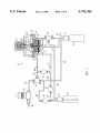
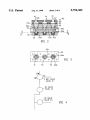
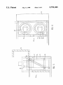
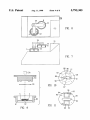
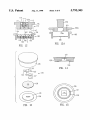
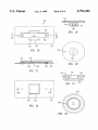
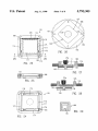
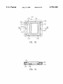
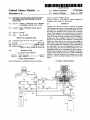
5 .792.305
9
10
cal and electrical operations of a typical decapsulator are in
the Model 250 Operation. Installation and Service Manual.
the content of which are incorporated herein by reference.
All components. other than springs. screws. and selected
valve components. are made of Te?on® plastic. glass.
(FIG. 19) with the etch cup 144. As in the earlier
embodiment. plug number 141 containing the device pack
age is slid into cavity 147 of cup 144 and an integral
depending ring 146 seals the cup to the etch head de?nition
gasket. The cup 144 ?ts snugly over the etch head outer
diameter.
PIGS. 16-18 show a ?xture for a plastic ball grid array
polypropylene. or PVC or other acid-resistant material. The
only metal components utilized are the springs and screws
which. where possible. are made of stainless steel. All ?ve
valves are pneumatically activated when decapsulation is
being performed as described above. All manifold ports are
the standard l/4-28 thread.
FIG. 12 illustrates a varient of the etch cup ?xmre seen in
FIG. 9. An electronic device package 3 in mounted within a
circular etch cup 100. particularly in a central aperture 102
of a Viton® or Te?on® circular alignment gasket 103 placed
against a bottom etch cup wall 105 in a ?rst cavity 104 of the
etch cup. The bottom etch cup wall 105 is apertured at 106
to receive acid ?ow from the etch head ori?ce 27 (FIG. 1).
A circular blank (unapertured) Viton or Te?on disk 107.
notched at 107a on its periphery for easy removal by a
tweezer or pry implement. covers alignment gasket 103.
Plug 110 slides into the cavity 104. Plug 110 includes a
(PBGA) package (illustrated as package 136 in FIG. 28)
which has package contact pads on the surface of the
10
overforce on the disk gasket and the package 3 in cavity 102.
while e?’ectively sealing the die package 3 except at the
aperture 106 through which the etchant ?ows. An O-ring
may be placed in groove 117. The etch cup 100. plunger 110
and other elements may be of various sizes. shapes and
thicknesses to accommodate various sized device packages.
FIG. 12A shows a vented etch cup assembly including etch
by etching. in the form of solder balls. A?xture 150 includes
an alignment plate or frame 151 specially pocketed for
solder ball clearance. The rim or peripheral edge of the
PBGA matches an internal mm 153 of the frame 151. The
15
20
PBGA is placed into the pocket 154 from the underside of
the frame (arrow 160). The halls face upward directly under
the plane of the frame top surface and spaced vertically
under a 90° angle bar 155 spanning the frame pocket and
connected to the frame by fasteners 149. The PBGA may be
held in the pocket preventing drop out by a I/:" (0.64 cm)
strip of Kapton® tape (not shown) on opposite sides of the
PBGA adjacent to the PBGA underside wall to be decapsu
lated by etching. Aram 230. as in FIG. 1. presses against the
horizontal portion 156 of angle bar 155 which with the
plunger 111 having an upper end 112 which is pressed by
spring 114 and ram 23a against disk 107 and in turn against
alignment gasket 103 to seal cavity 102. A ?ange stop 115
acting against ?ange 116 of the etch cup 100 prevents any
package opposite the package side wall to be decapsulated
25
alignment plate distributes the compressive force around the
PBGA edges and seals the frame with the cavity de?nition
gasket provided on the etch head as in the other embodi
ments. The vertical portion 157 of the angle bar serves as a
30
handle for removal of the ?xture from the etch head. using
tweezers or the like. After etching has decapsulated the
PBGA. it is preferred to leave the device in the frame until
after post-etch solvent cleaning. The back (top) of the
package containing the balls is completely protected and the
decapsulated device package is in an opened condition on
cup 100 and a modi?ed plug 100a and where apertures 119
the underside of the ?xture so that the device can be tested
and the absence of blank 107 allows for venting of the 35 and inspected. Alignment apertures 158 and 159 are pro
positive pressure in the bell jar 22 (FIG. 1) to stop acid ?ow
vided which with pins (not shown) on the etch plate.
properly align ?xture 150 with respect to the etch head.
FIGS. 23-26 and 30-31 illustrate a universal positioning
?xture 170 including a frame 171 which is capable of
when a chip sidewall is breached. Aram 23a is pushed down
through aperture 119a to hold the chip against the top edges
of acid aperture 106.
FIG. 13-15 illustrate an etch cup kit 120 for decapsulating
a transistor package 121 while providing containment for
extended cavities beyond the package side walls. The tran
sistor package 121 normally includes a die section 122. a
heat sink 123. and leads 124 extending therefrom. The
device package is placed in well 125 (FIG. 14) of the etch
cup 126 after leads 124 have been excised. Rubber or Te?on
blocks 127 may be positioned. after the package has been
placed in well 125. to ?ll the space between the package heat
sink and the etch head 131 in the etch plate 130. Ade?nition
gasket 128 may be used to reduce the initial etch cavity size
accurately locating medium (about 14 mm maximum length)
to large (about 40-63 mm maximum length) sized devices to
relieve the ongoing demand for custom ?xturing. This
?xture is expressly designed for multiple chip modules in
45
and slides provided can ?oat with adjustable friction or be
locked down for repeated usage. Components are made of
50
produced by the etching action. In this embodiment. the etch
cup 120 further includes an integral depending ring 129 for
sealing against the etch head 131. The well 125 acts as a
Te?on box creating an arti?cial side wall preventing the
etchant from exiting into the interior of hood cover 22 (FIG.
The embodiment disclosed provides for a device dimension
plus offset outlines up to 63 mm (2.50 inch) square; PBGA.
55
FIGS. 19 and 20 show a ?xture to decapsulate a dual-in
line package (DIP) or other array of leads extending from a
side or edge of the package opposite to the package side wall
to be etched. The well 140 in the etch cup cap 141 is
QFP. TQFP. DIP. SIP (single inline plastic) and PLCC
packages are easily accommodated; accuracy and repeat
ability of 0.2 mm (0.008 inch) is possible; and a 0.1 cm
graduated scale is supplied for user reference and adjust
ment.
As seen in FIG. 26 a sheet metal such as a stainless steel
sheet metal template rectangle 188 is placed ?ush on the etch
plate adjacent to etch head 130. locating the positioner on
center to the etch head. Pins 187 extend from the etch plate
189 through apertures 190. one aperture being oval and the
other circular. The edges 191 of the template abut a rim 192
provided with apertures 142 matching the lead pattern of the
package to be decapsulated. The etch cup surface mating
with the de?nition gasket may be lightly coated with high
reduce acid damage. A location pin 145 (FIG. 21) is
employed to accurately align hole(s) 143 in the cap 141
corrosion-resistant materials such as Te?on and stainless
steel. Fixturing is easily disassembled for routine cleaning.
1).
vacuum grease available from Dow Corning Chemical Co.
of Midland. Mich. Device leads may be similarly coated to
PBGA. QFP (quad ?at pack). TQFP (thin QFP). D11’. SIP
and PLCC (plastic leaded chip carrier) packages. These
multiple-die packages require ?exible ?xtun'ng and 01T
center alignment capabilities. Operator setups are simple
65
on the etch plate 185. the rim also forming a side wall of a
gasket groove surrounding the rim. The template is left on
the etch head and the ?xture is mounted thereon.