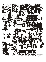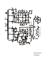
1
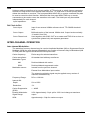
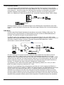
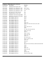
MAINTENANCE MANUAL
Model 39A
40MHz Arbitrary
Waveform Generator
October 2005 - Issue 1
This document contains information proprietary to
Wavetek and is provided solely for instrument
operation and maintenance. The information in this
document may not be duplicated in any manner
without the prior approval in writing from Wavetek.
Wavetek-Datron
Test and Measurement Division
Hurricane Way
Norwich
Norfolk NR6 6JB, U.K.
Tel: 44 1603 256600
Fax: 44 1603 256688
Table of Contents
Specifications
2
Safety
10
Installation
11
General
12
Circuit Descriptions
13
Calibration
18
Parts List
21
Component Layouts
29
Circuit Diagrams
31
1
Specifications
Note: This specification covers the whole series which includes 2- and 4- channel instruments;
the interchannel specifications only apply to the multi-channel instruments.
Specifications apply at 18−28ºC after 30 minutes warm−up, at maximum output into 50Ω
WAVEFORMS
Standard Waveforms
Sine, square, triangle, DC, positive ramp, negative ramp, sin(x)/x, pulse, pulse train, cosine,
haversine and havercosine.
Sine, Cosine, Haversine, Havercosine
Range:
0.1mHz to 16 MHz
Resolution:
0.1mHz or 7 digits
Accuracy:
10 ppm for 1 year
Temperature Stability:
Typically <1 ppm/ºC.
Output Level:
2.5mV to 10Vp−p into 50Ω
Harmonic Distortion:
<0.1% THD to 100kHz; <–65dBc to 20kHz
<–50dBc to 1MHz,
<−35dBc to 10MHz
<−30dBc to 16MHz
Non−harmonic Spurii:
<–65dBc to 1MHz, <–65dBc + 6dB/octave 1MHz to 16MHz
Range:
1mHz to 16MHz
Resolution:
1mHz (4 digits)
Accuracy:
± 1 digit of setting
Output Level:
2.5mV to 10Vp−p into 50Ω
Rise and Fall Times:
<25ns
Square
Triangle
Range:
0.1mHz to 100kHz
Resolution:
0.1mHz or 7 digits
Accuracy:
10 ppm for 1 year
Output Level:
2.5mV to 10Vp−p into 50Ω
Linearity Error:
<0.1% to 30 kHz
Ramps and Sin(x)/x
2
Range:
0.1mHz to 100kHz
Resolution:
0.1mHz (7 digits)
Accuracy:
10 ppm for 1 year
Output Level:
2.5mV to 10Vp−p into 50Ω
Linearity Error:
<0.1% to 30 kHz
Pulse and Pulse Train
Output Level:
2.5mV to 10Vp−p into 50Ω
Rise and Fall Times:
<25ns
Period:
Range:
Resolution:
Accuracy:
100ns to 100s
4-digit
±1 digit of setting
Range:
Resolution:
−99.99s to +99.99s
0.002% of period or 25ns, whichever is greater
Range:
Resolution:
25ns to 99.99s
0.002% of period or 25ns, whichever is greater
Delay:
Width:
Note that the pulse width and absolute value of the delay may not exceed the pulse period at any
time.
Pulse trains of up to 10 pulses may be specified, each pulse having independently defined width,
delay and level. The baseline voltage is separately defined and the sequence repetition rate is set
by the pulse train period.
Arbitrary
Up to 100 user defined waveforms may be stored in the 256K point non−volatile RAM.
Waveforms can be defined by front panel editing controls or by downloading of waveform data via
RS232 or GPIB.
Waveform Memory Size:
64k points per channel. Maximum waveform size is 64k
points, minimum waveform size is 4 points
Vertical Resolution:
12 bits
Sample Clock Range:
100mHz to 40MHz
Resolution:
4 digits
Accuracy:
± 1 digit of setting
Sequence
Up to 16 waveforms may be linked. Each waveform can have a loop count of up to 32,768.
A sequence of waveforms can be looped up to 1,048,575 times or run continuously.
Output Filter
Selectable between 16MHz Elliptic, 10MHz Elliptic, 10MHz Bessel or none.
3
OPERATING MODES
Triggered Burst
Each active edge of the trigger signal will produce one burst of the waveform.
Carrier Waveforms:
Maximum Carrier Frequency:
All standard and arbitrary
The smaller of 1MHz or the maximum for the selected
waveform.
40Msamples/s for ARB and Sequence.
Number of Cycles:
1 to 1,048,575
Trigger Repetition Rate:
0.005Hz to 100kHz internal
dc to 1MHz external.
Trigger Signal Source:
Internal from keyboard, previous channel, next channel or
trigger generator.
External from TRIG IN or remote interface.
Trigger Start/Stop Phase:
± 360° settable with 0.1° resolution, subject to waveform
frequency and type.
Gated
Waveform will run while the Gate signal is true and stop while false.
Carrier Waveforms:
All standard and arbitrary.
Maximum Carrier Frequency:
The smaller of 1MHz or the maximum for the selected
waveform. 40Msamples/s for ARB and Sequence.
Trigger Repetition Rate:
0.005Hz to 100kHz internal
dc to 1MHz external.
Gate Signal Source:
Internal from keyboard, previous channel, next channel or
trigger generator.
External from TRIG IN or remote interface.
Gate Start/Stop Phase:
± 360° settable with 0.1° resolution, subject to waveform
frequency and type.
Sweep
Frequency sweep capability is provided for both standard and arbitrary waveforms. Arbitrary
waveforms are expanded or condensed to exactly 4096 points and DDS techniques are used to
perform the sweep.
4
Carrier Waveforms:
All standard and arbitrary except pulse, pulse train and sequence.
Sweep Mode:
Linear or logarithmic, triggered or continuous.
Sweep Direction:
Up, down, up/down or down/up.
Sweep Range:
From 1mHz to 16 MHz in one range. Phase continuous.
Independent setting of the start and stop frequency.
Sweep Time:
30ms to 999s (3 digit resolution).
Marker:
Variable during sweep.
Sweep Trigger Source:
The sweep may be free run or triggered from the following
sources: Manually from keyboard. Externally from TRIG IN input or
remote interface.
Sweep Hold:
Sweep can be held and restarted by the HOLD key.
Multi channel sweep:
Any number of channels may be swept simultaneously but the
sweep parameters will be the same for all channels. Amplitude,
Offset and Waveform can be set independently for each channel.
Tone Switching
Capability provided for both standard and arbitrary waveforms. Arbitrary waveforms are expanded
or condensed to exactly 4096 points and DDS techniques are used to allow instantaneous
frequency switching.
Carrier Waveforms:
All waveforms except pulse, pulse train and sequence.
Frequency List:
Up to 16 frequencies from 1mHz to 10MHz.
Trigger Repetition Rate:
0.005Hz to 100kHz internal
dc to 1MHz external.
Usable repetition rate and waveform frequency depend on the tone
switching mode.
Source:
Internal from keyboard, previous channel, next channel or trigger
generator.
External from TRIG IN or remote interface.
Tone Switching Modes:
Gated:
The tone is output while the trigger signal is true and stopped, at the
end of the current waveform cycle, while the trigger signal is false.
The next tone is output when the trigger signal is true again.
Triggered:
The tone is output when the trigger signal goes true and the next
tone is output, at the end of the current waveform cycle, when the
trigger signal goes true again.
FSK:
The tone is output when the trigger signal goes true and the next
tone is output, immediately, when the trigger signal goes true again.
Using 2 channels with their outputs summed together it is possible to generate DTMF test
signals.
Trigger Generator
Internal source 0.005 Hz to 100kHz square wave adjustable in 10us steps. 3 digit resolution.
Available for external use from any SYNC OUT socket.
OUTPUTS
Main Output - One for each channel
Output Impedance:
50Ω
Amplitude:
5mV to 20Vp−p open circuit (2.5mV to 10Vp−p into 50Ω). Amplitude
can be specified open circuit (hi Z) or into an assumed load of 50Ω or
600Ω in Vpk−pk, Vrms or dBm.
Amplitude Accuracy:
2% ±1mV at 1kHz into 50Ω.
Amplitude Flatness:
±0.2dB to 200 kHz; ±1dB to 10 MHz; ±2.5dB to 16 MHz.
DC Offset Range:
±10V.DC offset plus signal peak limited to ±10V from 50Ω.
DC Offset Accuracy:
Typically 3% ±10mV, unattenuated.
Resolution:
3 digits or 1mV for both Amplitude and DC Offset.
5
Sync Out - One for each channel
Multifunction output user definable or automatically selected to be any of the following:
Waveform Sync:
(all waveforms)
A square wave with 50% duty cycle at the main waveform frequency, or
a pulse coincident with the first few points of an arbitrary waveform.
Position Markers:
(Arbitrary only)
Any point(s) on the waveform may have associated marker bit(s) set
high or low.
Burst Done:
Produces a pulse coincident with the last cycle of a burst.
Sequence Sync:
Produces a pulse coincident with the end of a waveform sequence.
Trigger:
Selects the current trigger signal. Useful for synchronizing burst or
gated signals.
Sweep Sync:
Outputs a pulse at the start of sweep to synchronize an oscilloscope or
recorder.
Phase Lock Out:
Used to phase lock two generators. Produces a positive edge at the 0°
phase point.
Output Signal Level:
TTL/CMOS logic levels from typically 50Ω.
Cursor/Marker Out
Adjustable output pulse for use as a marker in sweep mode or as a cursor in arbitrary waveform
editing mode. Can be used to modulate the Z−axis of an oscilloscope or be displayed on a
second ‘scope channel.
Output Signal Level:
Adjustable from nominally 2V to 14V, normal or inverted; adjustable
width as a cursor.
Output Impedance:
600Ω typical
INPUTS
Trig In
Frequency Range:
DC − 1MHz.
Signal Range:
Threshold nominally TTL level; maximum input ±10V.
Minimum Pulse Width:
50ns, for Trigger and Gate modes; 50us for Sweep mode.
Polarity:
Selectable as high/rising edge or low/falling edge.
Input Impedance:
10kΩ
Modulation In
Frequency Range:
DC – 100kHz.
Signal Range:
VCA: Approximately 1V pk−pk for 100% level change at maximum
output.
SCM: Approximately ± 1Vpk for maximum output.
Input Impedance:
Typically 1 kΩ.
Sum In
6
Frequency Range:
DC − 8 MHz.
Signal Range:
Approximately 2 Vpk−pk input for 20Vpk−pk output.
Input Impedance:
Typically 1kΩ.
Hold
Holds an arbitrary waveform at its current position. A TTL low level or switch closure causes the
waveform to stop at the current position and wait until a TTL high level or switch opening which
allows the waveform to continue. The front panel MAN HOLD key or remote command may also
be used to control the Hold function. While held the front panel MAN TRIG key or remote
command may be used to return the waveform to the start. The Hold input may be enabled
independently for each channel.
Input Impedance:
10kΩ
Ref Clock In/Out
Set to Input:
Input for an external 10MHz reference clock. TTL/CMOS threshold
level.
Set to Output:
Buffered version of the internal 10MHz clock. Output levels nominally
1V and 4V from 50Ω.
Set to Phase Lock:
Used together with SYNC OUT on a master and TRIG IN on a slave to
synchronise (phase lock) two separate generators.
INTER-CHANNEL OPERATION
Inter-channel Modulation:
The waveform from any channel may be used to Amplitude Modulate (AM) or Suppressed Carrier
Modulate (SCM) the next channel. Alternatively any number of channels may be Modulated (AM
or SCM) with the signal at the MODULATION input socket.
Carrier frequency:
Entire range for selected waveform.
Carrier waveforms:
All standard and arbitrary waveforms.
Modulation Types:
AM:
Double sideband with carrier.
SCM:
Double sideband suppressed carrier.
Modulation source:
Internal from the previous channel.
External from Modulation input socket.
The external modulation signal may be applied to any number of
channels simultaneously.
Frequency Range:
DC to >100 kHz.
Internal AM:
Depth:
0% to 105%
Resolution:
1%.
Carrier Suppression
(SCM):
> −40dB.
External Modulation
Signal Range:
VCA: Approximately 1V pk−pk for 100% level change at maximum
output.
SCM:
Approximately ± 1Vpk for maximum output.
7
Inter-channel Analog Summing:
Waveform Summing sums the waveform from any channel into the next channel.
Alternatively any number of channels may be summed with the signal at the SUM input socket.
Carrier frequency:
Entire range for selected waveform.
Carrier waveforms:
All standard and arbitrary waveforms.
Sum source:
Internal from the previous channel.
External from SUM IN socket.
Frequency Range:
DC to >8MHz.
External Signal Range:
Approximately 5Vpk−pk input for 20Vpk−pk output.
Inter-channel Phase locking:
Two or more channels may be phase locked together. Each locked channel may be assigned a
phase angle relative to the other locked channels. Arbitrary waveforms and waveform sequences
may be phase locked but certain constraints apply to waveform lengths and clock frequency
ratios. With one channel assigned as the Master and other channels as Slaves a frequency
change on the master will be repeated on each slave thus allowing multi−phase waveforms at the
same frequency to be easily generated.
DDS waveforms are those with 7 digits of frequency setting resolution, while Non−DDS
waveforms have 4 digits
Phase Resolution:
DDS waveforms:
0.1 degree
Non−DDS waveforms:
0.1 degree or 360 degrees/number of points whichever is the greater.
Phase Error:
All waveforms:
<±10ns
The signals from the REF IN/OUT socket and the SYNC OUT socket can be used to phase lock
two instruments where more than 4 channels are required.
Inter-channel Triggering:
Any channel can be triggered by the previous or next channel.
The previous/next connections can be used to ’daisy chain’ a trigger signal from a ‘start’ channel,
through a number of channels in the ‘chain’ to an ‘end’ channel. Each channel receives the trigger
out signal from the previous (or next) channel, and drives its selected trigger out to the next (or
previous) channel. The ‘end’ channel trigger out can be set up to drive the ‘start’ channel, closing
the loop.
In this way, complex and versatile inter−channel trigger schemes may be set up. Each channel
can have its trigger out and its output waveform set up independently. Trigger out may be
selected from Waveform End, Position Markers, Sequence Sync or Burst Done.
Using the scheme above it is possible to create a sequence of up to 64 waveform segments,
each channel producing up to 16 segments and all channels being summed to produce the
complete waveform at the output of channel 4.
INTERFACES
Full remote control facilities are available through the RS232 or GPIB interfaces.
8
RS232:
Variable Baud rate, 9600 Baud maximum. 9−pin D−connector.
IEEE−488:
Conforms with IEEE488.1 and IEEE488.2
GENERAL
Display:
20 character x 4 row alphanumeric LCD.
Data Entry:
Keyboard selection of mode, waveform etc.; value entry direct by
numeric keys or by rotary control.
Stored Settings:
Up to 9 complete instrument set−ups may be stored and recalled
from battery−backed memory. Up to 100 arbitrary waveforms can
also be stored independent of the instrument settings.
Size:
3U (130mm) height; 350mm width (2 and 4 channels),
212mm (½−rack) single channel; 335mm long.
Weight:
7.2 kg. (16 lb), 2 and 4 channels; 4.1kg (9lb) 1 channel.
Power:
230V, 115V or 100V nominal 50/60Hz, adjustable internally;
operating range ±14% of nominal; 100VA max. for 4 channels,
75VA max. for 2 channel, 40VA max. for 1 channel. Installation
Category II.
Operating Range:
+5°C to 40°C, 20−80% RH.
Storage Range:
−20°C to + 60°C.
Environmental:
Indoor use at altitudes up to 2000m, Pollution Degree 2.
Options:
19 inch rack mounting kit.
Safety:
Complies with EN61010−1.
EMC:
Complies with EN50081−1 and EN50082−1.
9
Safety
This generator is a Safety Class I instrument according to IEC classification and has been
designed to meet the requirements of EN61010−1 (Safety Requirements for Electrical Equipment
for Measurement, Control and Laboratory Use). It is an Installation Category II instrument
intended for operation from a normal single phase supply.
This instrument has been tested in accordance with EN61010−1 and has been supplied in a safe
condition. This instruction manual contains some information and warnings which have to be
followed by the user to ensure safe operation and to retain the instrument in a safe condition.
This instrument has been designed for indoor use in a Pollution Degree 2 environment in the
temperature range 5°C to 40°C, 20% − 80% RH (non−condensing). It may occasionally be
subjected to temperatures between +5° and −10°C without degradation of its safety. Do not
operate while condensation is present.
Use of this instrument in a manner not specified by these instructions may impair the safety
protection provided. Do not operate the instrument outside its rated supply voltages or
environmental range.
WARNING! THIS INSTRUMENT MUST BE EARTHED
Any interruption of the mains earth conductor inside or outside the instrument will make the
instrument dangerous. Intentional interruption is prohibited. The protective action must not be
negated by the use of an extension cord without a protective conductor.
When the instrument is connected to its supply, terminals may be live and opening the covers or
removal of parts (except those to which access can be gained by hand) is likely to expose live
parts. The apparatus shall be disconnected from all voltage sources before it is opened for any
adjustment, replacement, maintenance or repair.
Any adjustment, maintenance and repair of the opened instrument under voltage shall be avoided
as far as possible and, if inevitable, shall be carried out only by a skilled person who is aware of
the hazard involved.
If the instrument is clearly defective, has been subject to mechanical damage, excessive moisture
or chemical corrosion the safety protection may be impaired and the apparatus should be
withdrawn from use and returned for checking and repair.
Make sure that only fuses with the required rated current and of the specified type are used for
replacement. The use of makeshift fuses and the short−circuiting of fuse holders is prohibited.
This instrument uses a Lithium button cell for non−volatile memory battery back−up; typical life is
5 years. In the event of replacement becoming necessary, replace only with a cell of the correct
type, i.e. 3V Li/Mn02 20mm button cell type 2032. Exhausted cells must be disposed of carefully
in accordance with local regulations; do not cut open, incinerate, expose to temperatures above
60°C or attempt to recharge.
Do not wet the instrument when cleaning it and in particular use only a soft dry cloth to clean the
LCD window. The following symbols are used on the instrument and in this manual:−
Caution −refer to the accompanying documentation,
incorrect operation may damage the instrument.
terminal connected to chassis ground.
mains supply OFF.
l
mains supply ON.
alternating current.
10
Installation
Mains Operating Voltage
Check that the instrument operating voltage marked on the rear panel is suitable for the local
supply. Should it be necessary to change the operating voltage, proceed as follows:
1)
2)
3)
4)
5)
Disconnect the instrument from all voltage sources.
Remove the screws which retain the top cover and lift off the cover.
Change the transformer connections following the diagram below.
Refit the cover and the secure with the same screws.
To comply with safety standard requirements the operating voltage marked on the rear panel
must be changed to clearly show the new voltage setting.
6) Change the fuse to one of the correct rating, see below.
for 230V operation connect the live (brown) wire to pin 15
for 115V operation connect the live (brown) wire to pin 14
for 100V operation connect the live (brown) wire to pin 13
Fuse
Ensure that the correct mains fuse is fitted for the set operating voltage. The correct mains fuse
types are:
for 230V operation:
250 mA (T) 250V HRC
for 100V or 115V operation:
500 mA (T) 250V HRC
To replace the fuse, disconnect the mains lead from the inlet socket and withdraw the fuse drawer
below the socket pins. Change the fuse and replace the drawer.
The use of makeshift fuses or the short−circuiting of the fuse holder is prohibited.
Mains Lead
When a three core mains lead with bare ends is provided it should be connected as follows:−
Brown −
Mains Live
Blue −
Mains Neutral
Green / Yellow −
Mains Earth
WARNING! THIS INSTRUMENT MUST BE EARTHED
Any interruption of the mains earth conductor inside or outside the instrument will make the
instrument dangerous. Intentional interruption is prohibited. The protective action must not be
negated by the use of an extension cord without a protective conductor.
Mounting
This instrument is suitable both for bench use and rack mounting. It is delivered with feet for
bench mounting. The front feet include a tilt mechanism for optimal panel angle.
A rack kit for mounting in a 19” rack is available from the Manufacturers or their overseas agents.
11
General
Service Handling Precautions
Service work or calibration should only be carried out by skilled engineers. Please note the
following points before commencing work.
Most of the integrated circuits are CMOS devices and care should be taken when handling to
avoid damage by static discharge. Also most devices are surface mounted miniature components
with very fine leads on small pitches. These components must be removed and replaced with
great care to avoid damage to the PCB. It is essential that only the proper tools and soldering
equipment as recommended for surface mount components are used.
The decoupling capacitors associated with the integrated circuits are surface mounted on the
solder side of the PCB.
Dismantling the Instrument
WARNING!
Disconnect the instrument from all voltage sources before it is opened for adjustment or repair. If
any adjustment or repair of the opened instrument is inevitable it shall be carried out only by a
skilled person who is aware of the hazards involved.
12
1.
Remove the six screws retaining the top cover.
2.
The rear panel may be removed as follows. Disconnect the grey ribbon cable from PJ6 on
the GPIB PCB. Invert the instrument and remove the three screws securing the rear panel
and the nuts securing the 9-way RS232 connector to the rear panel. The panel may now
be tilted back to allow access. If the panel is to be completely removed the connectors
must be removed from PJ3, PJ7, PJ8 and PJ11, the blue and brown wires disconnected
from the mains inlet filter and the blue and brown wires unsoldered from the mains
transformer. Cut the ties holding the cable assembly to the side instrument chassis. The
panel is then completely free of the instrument.
3.
The front panel assembly may be removed as follows. Remove the connectors from PJ2,
PJ4, PJ12, PJ13 and PJ200 and desolder the screened cable from PJ202. Remove the
two nuts and bolts in the sides and two screws in the bottom of the instrument securing
the front panel assembly. The panel may now be drawn clear of the instrument.
4.
Main pcb removal. Remove all connectors from the pcb and desolder the screened cable
from PJ10. Tilt the rear panel away as in 2 above. Remove six screws and lift away the
main pcb. When re-assembling the instrument ensure that all fixings use the correct
fastenings.
Circuit Descriptions
General
The following sections should be read with reference to the block diagram and the circuit
diagrams.
Trig Out From
Previous Channel
Sync
Out
Trig Out From
Next Channel
Common
Hold In
Common
Remote
Control
GPIB/
RS232
Trig Out
Waveform
FPGA
INT
TRIG
Common
Cursor/
Marker
Out
16MHz
Elliptic
Filter
Lock Clock In/Out To
Other Channels
Bessel
Filter
12 bit
DAC
Waveform
RAM
Common
CPU
PLL
10MHz
CLK
DC Offset
Control
DAC,s
Common
Ext
Trig
Common
VCA
In
Common
SUM
In
Amp
10MHz
Elliptic
Filter
Zero Crossing
Comparator
Common
CLK
In/Out
VCA
SUM
Amplitude
Control
Main
Out
Amp
Output
Amp
Attenuators
Attenuators
DC
Offset
0-50dB
Attenuator
Amp
Sum Out
SUM Out
From Previous
Channel
Simplified Block Diagram
Principles of Operation
The instrument operates in one of two different modes depending on the waveform selected.
DDS mode is used for sine, cosine, haversine, triangle, sinx/x and ramp waveforms. Clock
Synthesis mode is used for square, pulse, pulse train, arbitrary and sequence.
In both modes the waveform data is stored in RAM. As the RAM address is incremented the
values are output sequentially to a Digital-to-Analogue Converter (DAC) which reconstructs the
waveform as a series of voltages steps which are subsequently filtered before being passed to
the main output connector.
The main difference between DDS and Clock Synthesis modes is the way in which the addresses
are generated for the RAM and the length of the waveform data.
13
Clock Synthesis Mode
In Clock Synthesis mode the addresses are always sequential (an increment of one) and the
clock rate is adjusted by the user in the range 40MHz to 0.1Hz. The frequency of the waveform is
clock frequency ÷ waveform length, thus allowing short waveforms to be played out at higher
repetition rates than long waveforms, e.g. the maximum frequency of a 4 point waveform is
40e6÷4 or 10MHz but a 1000 point waveform has a maximum frequency of40e6÷1000 or 40kHz.
Arbitrary waveforms have a user defined length of 4 to 65536 points. Squarewaves use a fixed
length of 2 points and pulse and pulse train have their length defined by the user selected period
value.
DDS Mode
In DDS mode (Direct Digital Synthesis) all waveforms are stored in RAM as 4096 points. The
frequency of the output waveform is determined by the rate at which the RAM addresses are
changed. The address changes are generated as follows:
The RAM contains the amplitude values of all the individual points of one cycle (360º) of the
waveform; each sequential address change corresponds to a phase increment of the waveform of
360º/4096. Instead of using a counter to generate sequential RAM addresses, a phase
accumulator is used to increment the phase.
On each clock cycle the phase increment, which has been loaded into the phase increment
register by the CPU, is added to the current result in the phase accumulator; the 12 most
significant bits of the phase accumulator drive the lower 12 RAM address lines, the upper 4 RAM
address lines are held low. The output waveform frequency is now determined by the size of the
phase increment at each clock. If each increment is the same size then the output frequency is
constant; if it changes, the output frequency changes as in sweep mode.
The generator uses a 38 bit accumulator and a clock frequency which is 238 x 10-4(~27.4878
MHz); this yields a frequency resolution of 0.1 mHz.
Only the 12 most significant bits of the phase accumulator are used to address the RAM. At a
waveform frequency of FCLK/4096 (~6.7MHz), the natural frequency, the RAM address increments
at every clock. At all frequencies below this (i.e. at smaller phase increments) one or more
addresses are output for more than one clock period because the phase increment is not big
enough to step the address at every clock. Similarly at frequencies above the natural frequency
the larger phase increment causes some addresses to be skipped, giving the effect of the stored
waveform being sampled; different points will be sampled on successive cycles of the waveform.
14
MPU and Memory
The majority of the digital hardware in the instrument is contained in 3 LSI devices, these being a
MicroProcessor Unit, IC3, and 2 Field Programmable Gate Arrays, IC10 and IC221.
The Z80180 MPU contains an 8 bit Z80 core, 2x16 bit counter-timers, 2x8 bit serial interfaces and
a memory management unit. The MPU is clocked at 12MHz by XTL1.
The MPU provides 20 memory address lines which are used to provide access to a total of 1M
bytes of memory, this comprising a 512k byte EPROM (IC4) and 5 128k byte rams IC5 – 9. The
EPROM is located at address 00000h and extends to 07FFFFh. The top 128k bytes are shared
by IC5 and the selection of ram or EPROM is controlled by the FPGA, IC10. The other 4 rams are
located at addresses 080000h to 0FFFFFh. IC9 is the system ram which contains all the essential
variables and work areas including the software stack. IC5 -8 is the non volatile store for all the
arbitrary waveforms and is not used for any other purpose. The MPU selects between the
memory devices via address decoders located in the FPGA at IC10.
The RS232 interface is provided directly by the MPU and is buffered to the rear panel connector
(PJ1) by IC1 and IC2.
One of the counter-timers provides a constant 0.5ms 'tick' to the MPU which is used to time all
the housekeeping functions, e.g. keyboard scan, knob control, as well as some generator
functions, e.g. frequency sweep. The second counter-timer is not used.
The FPGA, IC10, provides the port select signals to the GPIB board.
Keyboard, LCD and LEDs
The keyboard is interrogated every 10ms. This is done by reading the registers in IC12 and IC13.
If a key is down then one of the transistors Q6-Q13 will be on and the corresponding bits read
from IC12/IC13 will be high. The MPU decodes this to produce a key code which is passed to the
software. Multiple keys down are ignored. IC10 provides the port decode signals for access to
IC12 and IC13.
The knob is connected directly to the FPGA, IC10. This decodes the 4 states of the switches and
increments/decrements a counter. The counter is read and cleared every 10ms and the value and
sign passed to the software.
The 6 LEDs are driven directly from the outputs of IC18 and IC19 which are shift registers loaded
under CPU control by IC10.
The LCD is accessed via a bi-directional 4 bit port in IC10.
FPGA Waveform Generation
The FPGA, IC221, provides the complete waveform generation system including a 38-bit phase
accumulator (for DDS operation), a programmable divide-by-n register (for arbitrary waveform
playback), a 16-segment waveform sequencer, trigger/gate control logic, 20 bit re-loadable burst
counter, multi-instrument phase synchronisation logic and an 8-bit 16 port bi-directional MPU
interface.
Access is provided to the waveform RAM to allow the patterns to be written and the Sync and
Cursor/Marker output signals are generated.
All internal operations of the FPGA are clocked by the signal ARBCLK. Note that if this signal is
interrupted it is possible for the FPGA to become non-functional requiring the FPGA be
completely reset. The clock could be interrupted by a fault condition or by setting the CLOCK
BNC to INPUT and then providing an unacceptable clock. An unacceptable clock is any signal
which overrides the internal clock but produces a replacement which is less than 9MHz or greater
than 10.5MHz. This would happen if, for example, a DC voltage >2V was connected to the clock
input.
15
Trigger Generator
This is created by a counter-timer in IC10. The counter-timer produces a squarewave in the range
100kHz to 0.005Hz. The FPGA, IC221, may be set to use this as the internal trigger.
Power Supply
The transformer has two separate secondaries; one provides ± 15V by IC30 and IC31, the other
provides +5V by low drop-out regulator IC32 and −5V by IC33. The display backlight is driven by
a current source made up of Q22 and associated components and is approximately 150mA. IC34
provides local regulation for the +5V analogue. IC204 provides local regulation for the VCO.
IC226 provides local regulation for the PLL. PJ5 is a test point for the supply rails. Four PCB
mounted fuses protect the transformer secondaries under fault conditions.
Required values measured at PJ5:
pin 1: +5VCPU ± 0.2V
pin 2: 0V
pin 3: −5V ± 0.2V
pin 4: −15V ± 0.6V
pin 5: +5VA ± 0.2V
pin 6: +15V ± 0.6V
Waveform DAC and Filters
IC210 is a high speed 12-bit DAC whose data is latched on the rising edge of DACCLK. The
output current is 20mA fullscale giving 1Vp-p into 50Ω, from 0V to −1V. The DAC has an internal
−1.23V (−1.27V to −1.17V) reference. R218 sets the full-scale output current. An internal control
amplifier mirrors this with respect to the −5V rail.
L201,L202,L203 and associated components form the 16MHz 7-stage elliptic filter. The inductors
are factory set before board assembly and must not be adjusted. L204 provides sinx/x correction
and is adjusted at initial calibration.
L205,L206,L207 and associated components form the 10MHz 7-stage elliptic filter. The inductors
are factory set before board assembly and must not be adjusted. L208 provides sinx/x correction
and is adjusted at initial calibration.
L209, C252 and C253 form a Bessel filter. L209 is also factory preset.
Amplitude Control, Sum and Modulation
IC215 is a 4-quadrant multiplier driven differentially via IC211. The main signal is at M and is 0V
to −1V; a dc reference, M1, of half this is generated by IC200-A. Amplitude is controlled by
IC218-A; with the output set to maximum the voltage at its output is approximately 1V.
External AM is selected by IC214-A and is summed with the amplitude control voltage at the input
of IC218-A.
Sum is selected by IC214-C and the external signal is summed at the multiplier output via its
Z input.
IC212 and IC213 form the sum input attenuator.
Amplifiers and Attenuators
With the amplitude at maximum the signal at the output of the multiplier is approximately 1Vp-p.
IC219 gives a gain of 5.5 to give 5.5Vp-p and IC220 gives a gain of 3.8 to give 20Vp-p.
IC218-B provides DC offset for the main output; when set to maximum, i.e. +10V, IC218-B’s
output will be approximately −10V and its input approximately –3.6V.
Relays RL201 and RL202 select 20dB output attenuators and IC217 selects an intermediate
−10dB attenuator.
16
Zero Crossing Detector
IC201 is a comparator with positive feedback via R203. M is the signal selected by IC211 and M2
is the signals dc mid-point which is buffered by IC200-B. This circuit is used to detect zero
crossing of high frequency DDS waveforms of sine, ramp or triangle and sent to the FPGA.
Control DACs
IC27 is a 12-bit voltage output DAC with internal 2V reference. IC115 provides a bi-polar output of
± 3.3V. IC28 multiplexes the DAC output voltage onto the appropriate hold capacitor. FET input
amplifiers IC29 buffer the voltages on the hold capacitors.
IC208 is a quad 8-bit DAC. IC209D provides a 3.3V reference to give 0 to 3.3V DAC output.
IC209-A, -B and -C give gain and/or offset. VR200 gives coarse adjustment of the multiplier offset
and is only adjusted at initial calibration with the default calibration values present.
The voltage at each DAC output is controlled by the MPU which calculates each value from a
combination of the instrument set up and the calibration constants stored in EEPROM.
Reference Clock
IC105 is an integrated 10MHz voltage controlled crystal oscillator. If an external clock is applied,
C48 is charged up via D5 blocking the internal clock.
Phase-Locked-Loop and VCO
IC203 is a VCO tuned by varicap diodes D209-212. The range is 20MHz to 40MHz for square
and arbitrary waveforms and fixed at 27.48779MHz in the DDS mode. Comparator IC205 gives
TTL output levels.
IC206 is a PLL IC and has internal dividers for both inputs which are set by the MPU. Phase
comparison is done at 3kHz in PLL mode and slightly higher in DDS mode. IC15 is the loop filter
which drives the VCO. LED2 is out when the loop is in lock.
Inputs and Outputs
IC21 is a hex Schmitt; -A, -B, -D and -E are used for the Trig In and Hold In inputs. The Sync
output has four gates in parallel, IC202.
IC23 is an octal 3-state buffer. When Clock In/Out is an output the top four buffers are enabled
and the bottom four disabled. When Clock In/Out is an input the top four buffers are disabled and
the bottom four enabled.
The Zmod output high is set by the three digital signals at the input of IC16-A. IC16-A provides
gain to give a maximum output high of 14V. When Q14 is on, the output is low; when turned off
the output goes high until D2 conducts, clamping output high to the required level.
17
Calibration
All parameters can be calibrated without opening the case, i.e. the generator offers ‘closed−box’
calibration. All adjustments are made digitally with calibration constants stored in EEPROM. The
calibration routine requires only a DVM and a frequency counter and takes no more than a few
minutes.
The crystal in the timebase is pre−aged but a further ageing of up to ±5ppm can occur in the first
year. Since the ageing rate decreases exponentially with time it is an advantage to recalibrate
after the first 6 month’s use. Apart from this it is unlikely that any other parameters will need
adjustment.
Calibration should be carried out only after the generator has been operating for at least 30
minutes in normal ambient conditions.
Equipment Required
• 3½ digit DVM with 0.25% DC accuracy and 0.5% AC accuracy at 1kHz.
• Frequency counter capable of measuring 10.00000MHz.
The DVM is connected to the MAIN OUT of each channel in turn and the counter to any SYNC
OUT.
Frequency meter accuracy will determine the accuracy of the generator’s clock setting and
should ideally be ±1ppm.
Calibration Procedure
The calibration procedure is accessed by pressing the calibration… soft−key on the
UTILITY screen.
CALIBRATION SELECTED
Are you sure ?
◊password… tests…◊
◊exit continue◊
The software provides for a 4−digit password in the range 0000 to 9999 to be used to access the
calibration procedure. If the password is left at the factory default of 0000 no messages are
shown and calibration can proceed as described in the Calibration Routine section; only if a
non−zero password has been set will the user be prompted to enter the password.
Setting the Password
On opening the Calibration screen press the password… soft−key to show the password
screen:
ENTER NEW PASSWORD
−−−−
Enter a 4−digit password from the keyboard; the display will show the message NEW PASSWORD
STORED! for two seconds and then revert to the UTILITY menu. If any keys other than 0−9
are pressed while entering the password the message ILLEGAL PASSWORD! will be shown.
Using the Password to Access Calibration or Change the Password
With the password set, pressing calibration… on the UTILITY
ENTER PASSWORD
----
18
screen will now show:
When the correct password has been entered from the keyboard the display changes to the
opening screen of the calibration routine and calibration can proceed as described in the
Calibration Routine section. If an incorrect password is entered the message INCORRECT
PASSWORD! is shown for two seconds before the display reverts to the UTILITY menu.
With the opening screen of the calibration routine displayed after correctly entering the password,
the password can be changed by pressing password... soft−key and following the procedure
described in Setting the Password. If the password is set to 0000 again, password protection is
removed.
The password is held in EEPROM and will not be lost when the memory battery back−up is lost.
In the event of the password being forgotten, contact the manufacturer for help in resetting the
instrument.
Calibration Routine
The calibration procedure proper is entered by pressing continue on the opening Calibration
screen; pressing exit returns the display to the UTILITY menu. Pressing tests… calls a
menu of basic hardware checks used at production test which are self-explanatory. At each step
the display changes to prompt the user to adjust the rotary control or cursor keys, until the
reading on the specified instrument is at the value given. The cursor keys provide coarse
adjustment, and the rotary control fine adjustment. Pressing next increments the procedure to
the next step; pressing CE decrements back to the previous step. Alternatively, pressing exit
returns the display to the last CAL screen at which the user can choose to either save new
values, recall old values or calibrate again.
The first two displays (CAL 00 and CAL 01) specify the connections and adjustment method. The
next display (CAL 02) allows the starting channel to be chosen in multi-channel instruments;
ignore CAL02 in this instrument and step on to CAL03. The subsequent displays, CAL 03 to
CAL 55, permit all adjustable parameters to be calibrated.
The full procedure is as follows:
CAL 03
CH1. DC offset zero.
Adjust for 0V ± 5mV.
CAL 04
CH1. DC offset at + full scale.
Adjust for + 10V ± 10mV.
CAL 05
CH1. DC offset at − full scale.
Check for –10V ± 3%
CAL 06
CH1. Multiplier zero.
Adjust for minimum Volts AC
CAL 07
CH1. Multiplier offset.
Adjust for 0V ± 5mV.
CAL 08
CH1. Waveform offset.
Adjust for 0V ± 5mV.
CAL 09
CH1. Output level at full−scale
Adjust for 10V ± 10mV.
CAL 10
CH1. 20dB attenuator
Adjust for 1V ± 1mV.
CAL 11
CH1. 40dB attenuator
Adjust for 0.1V ± .1mV.
CAL 12
CH1. 10dB attenuator
Adjust for 2.236V AC ± 10mV.
CAL 13
CH1. Not used.
CAL 14
CH1. Not used.
CAL 15
CH1. Not used.
CAL 55
Clock calibrate
Adjust for 10.00000 MHz at SYNC OUT.
Service Adjustments
The following 3 sections contain information about adjustments which are normally done once
only at the factory. These may need to be repeated if a component in the relevant area is
changed.
19
VCO Adjustment
This should not normally be necessary and L6 is sealed at the factory. However if a problem is
suspected or components in this circuit have been changed carry out the following test first.
Set the output to 10MHz squarewave and check that the voltage at TP200.3 is −9.5V to −10.5V.
Check LED 200 is off.
Only if the voltage is outside these limits should L200 be adjusted to −10V ±0.2V. L6 core must
then be resealed again to reduce phase noise caused by mechanical vibration. Use only noncorrosive silicon rubber.
VR200 Adjustment
Not normally necessary. Must only be adjusted with the default calibration values loaded or
CAL07 set to 0128. At CAL07 adjust VR200 for 0Vdc ± 5mV.
Amplitude Flatness
This should not normally be necessary. Set to 20Vpk-pk and use a 50Ohm terminator, frequency
to 100kHz sinewave. Adjust oscilloscope to show exactly 6 divisions. Frequency to 10.00000MHz
and adjust L208 for exactly 6 divisions. Frequency to 10.1MHz and adjust L204 for exactly 6
divisions. These two adjustments should only be done using a high quality oscilloscope with a
bandwidth of at least 100MHz.
Remote Calibration
Calibration of the instrument may be performed over the RS232 or GPIB interface. To completely
automate the process the multimeter and frequency meter will also need to be remote controlled
and the controller will need to run a calibration program unique to this instrument.
The remote calibration commands allow a simplified version of manual calibration to be
performed by issuing commands from the controller. The controller must send the CALADJ
command repeatedly and read the dmm or frequency meter until the required result for the
selected calibration step is achieved. The CALSTEP command is then issued to accept the new
value and move to the next step.
While in remote calibration mode very little error checking is performed and it is the controllers
responsibility to ensure that everything progresses in an orderly way. Only the following
commands should be used during calibration.
WARNING: Using any other commands while in calibration mode may give unpredictable results
and could cause the instrument to lock up, requiring the power to be cycled to regain control.
CALIBRATION <cpd> [,nrf]
The calibration control command. <cpd> can be one of three
sub−commands:−
START
Enter calibration mode; this command must be issued before any other
calibration commands will be recognised.
SAVE
Finish calibration, save the new values and exit calibration mode.
ABORT
Finish calibration, do not save the new values and exit calibration mode.
<nrf> represents the calibration password. The password is only required
with CALIBRATION START and then only if a non−zero password has
been set from the instrument’s keyboard. The password will be ignored,
and will give no errors, at all other times.
It is not possible to set or change the password using remote commands.
CALADJ <nrf>
Adjust the selected calibration value by <nrf>. The value must be in the
range −100 to +100. Once an adjustment has been completed and the
new value is as required the CALSTEP command must be issued for the
new value to be accepted.
CALSTEP
Step to the next calibration point.
For general information on remote operation and remote command formats, refer to the Instrument
instruction manual remote operation sections.
20
Parts List
PCB ASSY - KEYBOARD (44912-0710)
Part Number
Description
Position
22224-0010
ENCODER ROT 36 POS W/O DETENT
SW1
22226-0101
KEYSWITCH - ALPS SKHHBW
K5-12, 20, 21, 30, 31, 48
22226-0150
KEYSWITCH LIGHT GREY
K1, 2, 4, 13-19, 22-29, 32-47, 49
23202-1680
RES 680RF W25 MF 50PPM
R1-3,5,11,12
23382-2470
RES PS/H 5K0 CERMET MIN
VR3
25061-0200
LED - T1 ROUND (3mm) - RED
LD1-5,11
35555-3010
PCB - KEYBOARD
43171-2230
CONN ASSY KB/MAIN 34W
PCB ASSY – MAIN (44912-0720)
Part Number
Description
Position
10366-9701
ADHESIVE MTG PADS 25 x 12MM
FOR BATTERY
20613-0006
WASHER (SIL-PAD) TO220
FOR SK200
20613-0007
WASHER (SIL-PAD) TO220 PLAIN
FOR SK2
20670-0135
CLIP GP02 FOR PCB MTG H/SINKS
FOR SK2-5,200
20670-0310
HEATSINK PCB MTG 38MM PLAIN
SK200 FOR IC220
20670-0320
HEATSINK PCB MTG 50MM PLAIN
SK2,3,4,5
20670-0340
HEATSINK TO220 CLIP-ON 29DEG/W
SK8
22010-0610
BATTERY 3V LITH 20MM BUTTON
BATT
22040-0920
BEAD FERRITE – LEADED
FB1,200-206
22042-0260
INDUCTOR 2.7UH
L208
22042-0261
INDUCTOR 2.07UH BLK
L205
22042-0262
INDUCTOR 2.0UH WHT
L206
22042-0263
INDUCTOR 1.78UH GRN
L207
22042-0271
INDUCTOR 1.545UH RED
L209
22042-0290
INDUCTOR 1.2UH
L204
22042-0291
INDUCTOR 1.322UH YEL
L201
22042-0292
INDUCTOR 1.157UH RED
L202
22042-0293
INDUCTOR 1.06UH BLUE
L203
22042-0300
INDUCTOR 0.47UH
L200
22240-0020
RELAY TYPE 53/5 (24V)
RL201,202
22240-0050
RELAY TYPE 47 (24VDC)
RL200,203,204,205
22315-0450
FUSE 500mAT SUBMIN PCB MNT
FS3,4
22315-0453
FUSE 1.5AT SUBMIN PCB MTG
FS1, 2
22573-0041
HEADER 2WAY STR SIL STD/GOLD
LK1, 2, TP1, TP201/202
22573-0048
HEADER 3WAY STR SIL STD/GOLD
PJ202 (CENTRE PIN REMOVED)
21
PCB ASSY – MAIN (44912-0720) continued/...
Part Number
Description
Position
22573-0070
HEADER 4WAY STR SIL STD
TP200
22573-0202
HEADER 2 WAY STRAIGHT .156P
PJ3, 7, 200
22573-0204
HEADER 4 WAY STRAIGHT .156P
PJ11/12, PJ13
22573-0206
HEADER 6 WAY STRAIGHT .156P
PJ8
22574-0450
SKT 9W R/A D-TYPE (CLIP IN)
PJ1
22575-0038
HEADER 6WAY STR SIL STD
PJ5
22575-0065
HEADER 20 WAY(2X10) STR SKEL
PJ6
22575-0100
HEADER 34 WAY(2X17) STR SKEL
PJ2, 4
23105-0010
RES SM0805 1R00F W1
R276
23105-0022
RES SM0805 2R20F W1
R275
23105-0068
RES SM0805 6R80F W1
R274
23105-0100
RES SM0805 10R0F W1
R25
23105-0215
RES SM0805 21R5F W1
R204, 273
23105-0510
RES SM0805 51R0F W1
R200, 237, 238, 239, 244, 253, 278, 300
23105-0620
RES SM0805 62R0F W1
R219
23105-0680
RES SM0805 68R0F W1
R247, 250, 272, 277
23105-0820
RES SM0805 82R0F W1
R269
23105-1100
RES SM0805 100RF W1
R7, 225, 227, 229, 230, 249
23105-1110
RES SM0805 110RF W1
R48-51, 251, 266
23105-1130
RES SM0805 130RF W1
R58, 62
23105-1150
RES SM0805 150RF W1
R201, 213-216
23105-1180
RES SM0805 180RF W1
R220, 294, 309
23105-1215
RES SM0805 215RF W1
R248, 271
23105-1220
RES SM0805 220RF W1
R3, 59, 223, 312
23105-1470
RES SM0805 470RF W1
R36, 37, 252, 281, 293
23105-1510
RES SM0805 510RF W1
R226, 297
23105-1620
RES SM0805 620RF W1
R24, 307
23105-1680
RES SM0805 680RF W1
R311
23105-2100
RES SM0805 1K00F W1
R5,10,27,33,34,56,57,60,61,202,218,228,304-305
23105-2130
RES SM0805 1K30F W1
R268
23105-2150
RES SM0805 1K50F W1
R292
23105-2180
RES SM0805 1K80F W1
R267, 291
23105-2200
RES SM0805 2K00F W1
R222, 231, 287
23105-2220
RES SM0805 2K20F W1
R280
23105-2240
RES SM0805 2K40F W1
R19, 28, 243
23105-2270
RES SM0805 2K70F W1
R18, 22, 26, 232, 299
22
PCB ASSY – MAIN (44912-0720) continued/...
Part Number
Description
Position
23105-2300
RES SM0805 3K00F W1
R30, 310
23105-2470
RES SM0805 4K70F W1
R23, 282, 288, 289, 290, 295, 296, 298
23105-2510
RES SM0805 5K10F W1
R233, 242, 306
23105-2560
RES SM0805 5K60F W1
R240, 270
23105-3100
RES SM0805 10K0F W1
R1, 2,4,6,11-14,32, 35 55,205,207,209-211,235
23105-3120
RES SM0805 12K0F W1
R217
23105-3150
RES SM0805 15K0F W1
R221, 236, 241, 279
23105-3200
RES SM0805 20K0F W1
R53, 54, 154
23105-3270
RES SM0805 27K0F W1
R206, 212
23105-3330
RES SM0805 33K0F W1
R155
23105-3470
RES SM0805 47K0F W1
R29, 203, 208, 234, 301, 302, 303
23105-3510
RES SM0805 51K0F W1
R17
23105-4100
RES SM0805 100KF W1
R8, 16, 20, 21, 38
23105-4200
RES SM0805 200KF W1
R15
23105-5100
RES SM0805 1M00F W1
R9
23105-6100
RES SM0805 10M0F W1
R45, 52, 224
23202-0039
RES 3R90F W25 MF 50PPM
R72
23202-0100
RES 10R0F W25 MF 50PPM
R70
23202-0102
RES 10R2F W25 MF 50PPM
R262, 265
23202-1240
RES 240RF W25 MF 50PPM
R40
23202-1750
RES 750RF W25 MF 50PPM
R39
23202-2220
RES 2K20F W25 MF 50PPM
R71
23206-0412
RES 41R2F W60 MF 50PPM
R260, 261, 263, 264
23206-1200
RES 200RF W60 MF 50PPM
R256-259
23222-0047
RES 4R70J W33 MF FUSIBLE
R254, 255
23301-0443
RES NETWK SIL 22K X 8
RP1-3
23377-2220
RES PS/H 2K2 CF 10MM
VR200
23424-0443
CAP10NZ 1KV CER D10 P5
C70, 71
23427-0268
CAP22PJ 100V CER NPO P2.5
C1, 4, 50, 51, 206, 207
23427-0331
CAP1N0K 63V CER HI K P5
C311
23427-0593
CAP82PG 100V CER NPO P2.5
C233
23427-9205
CAP47PJ 100V CER NPO P2.5
C245, 276, 293, 318
23427-9209
CAP33PJ 100V CER NPO P2.5
C8, 246, 248, 250, 251
23427-9218
CAP 330PK 100V CER MED K P2.5
C253
23428-0082
CAP8P2C 100V CER NPO P2.5
C232, 234, 270, 319
23428-0390
CAP39PG 100V CER N150 P2.5
C240, 242, 244, 252, 254
23
PCB ASSY – MAIN (44912-0720) continued/...
Part Number
Description
Position
23428-0560
CAP56PG 100V CER N150 P2.5
C239, 247
23428-1100
CAP 100PG 100V CER NPO P2.5
C12, 235, 241, 249
23428-1150
CAP 150PG 100V CER N150 P2.5
C236
23428-1180
CAP 180PG 100V CER N750 P2.5
C238, 243
23461-0015
CAP SM0805 10NK 50V CER X7R
C48, 210, 213, 216, 218, 219, 221, 224, 225,
271, 288, 289, 290, 292, 320, 322
23461-0020
CAP SM0805 100NZ 50V CER Y5V
C3, 6, 9-11,16-41,52-57,60-63,66,67, 81, 141,
155, 200, 201,203, 204, 205,208, 209,211, 214,
215, 217, 220, 229, 230, 255, 256, 257, 261,
262, 263, 265, 267-269, 272-275, 277-279, 281,
283, 291, 294, 295,300-310, 312-317, 321
23557-0612
CAP 1U0 100V ELEC RE2 P2
C15
23557-0647
CAP 10U 35V ELEC RE2 P2
C2, 5, 13, 14, 42, 43, 76, 77, 79, 212, 264, 266,
280, 282, 285, 286
23557-0658
CAP 100U 25V ELEC RE2 P2.5
C78, 80
23557-0660
CAP 2200U 16V ELEC RE2 P5
C75
23557-0664
CAP 1000U 35V ELEC RE2 P5
C72, 73
23557-0673
CAP 22U 35V ELEC RE2 P2
C7, 202, 231
23557-9122
CAP 4700U 16V ELEC RE2 P7.5
C74
23620-0242
CAP 22NJ 100V P/E P5
C227
23620-0246
CAP 100NK 63V P/E P5
C228
23620-0249
CAP 330NK 63V P/E P5
C64, 65
23620-0252
CAP 2N2K 63V P/E P5
C226
25021-0901
DIO 1N4148 B/R
D1-3, 5-9, 200-207, 213, 214
25061-0200
LED - T1 ROUND (3mm) - RED
LED1, LD200
25115-0907
DIO 1N4002 B/R
D10-13
25130-9201
DIO ZEN 6V2 W5
D208
25131-0224
DIO ZEN 18V 1W3
D14, 15
25131-0227
DIO ZEN 6V8 5W
D16-18
25174-0224
DIO SM VARICAP BB148
D209-212
25211-9302
RECTIFIER BRIDGE W02G
BR1
25334-0011
TRAN PNP TIP30
Q22
25336-5590
TRAN PNP BC559C
Q1, 3, 6-13
25377-5490
TRAN NPN BC549C
Q2, 4, 5, 14, 15, 20, 21, 200-205
27103-0041
IC NE527N
IC201
27103-1020
IC SM AD8561AR
IC205
27106-0517
IC NE5532N
IC218
24
PCB ASSY – MAIN (44912-0720) continued/...
Part Number
Description
Position
27106-0633
IC EL2099CT
IC220
27106-1110
IC SM LM358M DUAL OP AMP
IC16, 200
27106-1160
IC SM LM324M OP AMP
IC209
27106-1170
IC SM AD8055AR OP AMP
IC219
27106-1180
IC SM AD8056AR OP AMP
IC25, 216
27106-1210
IC SM LMC662CM
IC29, 115
27107-0071
IC SM TL071 BIFET OP AMP
IC207
27151-1010
IC AD835AN
IC215
27153-1050
IC SM LTC1257CS8
IC27
27153-1060
IC SM TLC5620CD DAC
IC208
27153-1070
IC SM HI5735KCB DAC
IC210
27158-0020
IC SM MC145170D
IC206
27158-0030
IC SM MC12148D
IC203
27160-0011
IC V/REG 78L05 TO92
IC108, 204, 226
27160-0013
IC V/REG 7815 TO220
IC30
27160-0020
IC V/REG 7915 T0220
IC31
27160-0210
IC V/REG LM337 TO220
IC33
27160-0460
IC V/REG L4941BV
IC32, 34
27227-0510
IC SM 4051
IC28
27227-0940
IC SM 4094
IC18, 19
27236-0520
IC SM 74HC4052
IC211, 212, 217
27236-0530
IC SM 74HC4053
IC213, 214
27238-0000
IC SM 74HCT00
IC202
27238-0140
IC SM 74HCT14
IC11, 21
27239-0000
IC SM 74HC00
IC22
27239-0320
IC SM 74HC32
IC14, 15, 20
27239-2400
IC SM 74HC240
IC23
27239-3730
IC SM 74HC373
IC12, 13
27253-0020
IC SM 64180
IC3
27253-0050
IC SM 14C88
IC1
27253-0060
IC SM 14C89
IC2
27400-0140
IC 27C4001 512Kx8 EPROM
IC4
27403-0010
IC SM 93C46 1K(64x16) EEPR
IC17
27410-0460
IC SM 32KX8 RAM 15ns
IC222-225
27412-0080
IC SM XCS10-4TQ144C
IC221
27412-0090
IC SM XCS05-3VQ100C
IC10
27413-0430
IC SM 128Kx8 RAM 70ns
IC5-9
25
PCB ASSY – MAIN (44912-0720) continued/...
Part Number
Description
Position
28151-0010
BUZZER
BUZZ
28502-0020
RESONATOR CERAMIC 12MHZ
XTL1
28515-0070
OSC MODULE 10MHz VCXO
IC105
31331-9030
SCREEN PCB MOUNT
S205, 206
35555-3210
PCB - MAIN
FRONT PANEL ASSY
Part Number
Description
Position
20030-0263
WASHER M3 ZPST
BEZEL
20030-9201
WASHER 6BA x 1/32in. FIBRE
LCD FIXING
20030-9202
WASHER 6BA x 1/16in. FIBRE
LCD FIXING
20038-9501
WASHER M3 SPRING
KEYBOARD PCB/FRONT PANEL
20065-0090
SCREW K22 X 5 PT LN1442 PNHDZ
BEZEL FIXING
20210-0104
NUT M2.5 ZPST
LCD FIXING
20234-0027
SCREW M3 X 6 PNHDPZ ZPST
KEYBOARD PCB/FRONT PANEL, BEZEL
20234-0040
SCREW M2.5 X 12MML PNHDPZ ZPST
LCD FIXING
20612-0011
WASHER FIBRE M3
KEYBOARD PCB/FRONT PANEL
20620-0010
CLIP - ENCODER KNOB
22219-0090
SWITCH ROCKER DPST GREY
22573-0056
HEADER 16WAY STR SIL STD
FOR DISPLAY
22575-0202
SKT 2W .156 20AWG (YELLOW) IDT
MAIN PCB PJ200A & PJ200B, PJ7
22575-0204
SKT 4W .156 20AWG (YELLOW) IDT
INTERFACE 1 PJ6
22588-0004
BNC SKT BKHD 50R STANDARD
26100-0160
LCD 20 X 4 BACK LIT
31711-0180
BEZEL
33331-7210
FRONT PANEL
33331-7290
OVERLAY FRONT PANEL
37113-2030
KEYCAP 8X3MM LIGHT GREY
37151-0430
KNOB ENCODER LIGHT GREY
43171-1400
CONN ASSY 2 WAY 285MM
PJ12, 200 (MAIN)
43171-1401
CONN ASSY 2 WAY 195MM
PJ13 (MAIN)
43171-2210
CONN ASSY CRIMPED
26
REAR PANEL ASSY
Part Number
Description
Position
20037-0401
SOLDER TAG SHAKEPROOF - 4BA
EARTH
20038-9502
WASHER M4 SPRING EARTH
20063-0010
SCREW NO6 X 3/8 NIB HDPZ ST/AB
20210-0102
NUT M4 ZPST EARTH
20213-0040
CAPTIVE NUT SPIRE NO.6
20223-9001
SCREW M3 X 8 RAISED CKHDPZ
MAINS INLET
20236-0010
SCREW M4 X 12 TAMPERPROOF
EARTH
22115-0340
TRANSFORMER
22520-0170
FILTER - IEC INLET + FUSE - 1A
20037-0401
SOLDER TAG SHAKEPROOF - 4BA
EARTH
20038-9502
WASHER M4 SPRING
EARTH
20063-0010
SCREW No 6 x 3/8 NIB HDPZ ST/AB
TRANSFORMER
22588-0004
BNC SKT BKHD 50R STANDARD
33331-7430
REAR PANEL PRINTED
43171-1401
CONN ASSY 2 WAY 195MM
TRANSFORMER
PJ1, 3, 11 MAIN
CASING AND OTHER ITEMS
Part Number
Description
Position
10144-0007
CABLE COAX 50Ω 2.6MM RG316/U
BNC TO PCB MAIN (PJ202)
20030-0266
WASHER M4 ZPST
RUBBER FEET
20037-0301
WASHER M3 SHK/PROOF I/T ZPST
CHASSIS/F. PANEL
20038-9501
WASHER M3 SPRING
CHASSIS/SPACERS, PCB/SPACERS,
FRONT PANEL
20062-0700
SCREW NO 6 X 3/8 RFLNGPZ ST/AB
CHASSIS/REAR PANEL
20063-0010
SCREW NO6 X 3/8 NIB HDPZ ST/AB
CASE UPPER
20210-0101
NUT M3 ZPST
FRONT PANEL
20213-0040
CAPTIVE NUT SPIRE NO.6
CHASSIS
20234-0012
SCREW M3 X 8 PNHDPZ ZPST
CHASSIS
20234-0027
SCREW M3 X 6 PNHDPZ ZPST
CHASSIS/SPACERS, PCB/SPACERS
20234-0029
SCREW M4 X 12 PNHDPZ ZPST
FEET
20612-0011
WASHER FIBRE M3
PCB/SPACERS
20661-0219
SPACER HEX M3 x 15 NPBR
20662-0201
BRACKET PLAS FOOT 3786-7001
20662-0520
FOOT PVC PV2629 BLACK
22315-0232
FUSE 250MA TL HRC S/F
230V VERSIONS
22315-0233
FUSE 500MA TL HRC S/F
115V VERSIONS
27
CASING AND OTHER ITEMS continued/...
Part Number
Description
Position
22491-0120
MAINS LD 2M ST IEC/UK PLUG 5A
UK VERSIONS
22491-0270
MAINS LD 2M ST IEC/EURO PLUG
EURO VERSIONS
22491-0040
MAINS LD 2M ST IEC/USA PL
USA VERSIONS
22469-0203
SOLDER TERMINAL PIN (18-0223K)
DISPLAY CABLE
22575-0202
SKT2W .156 20AWG (YELLOW )IDT
PJ3, 7,11,12,200 ON MAIN
22575-0204
SKT4W .156 20AWG (YELLOW) IDT
PJ13 ON MAIN
22575-0206
SKT6W .156 20AWG (YELLOW) IDT
PJ8 ON MAIN
33171-0130
SPRING FOOT
33537-0900
CASE UPPER
33537-0910
CASE LOWER
43171-1430
CONN ASSY GPIB/MAIN 20W
43171-2250
CONN ASSY DIS/MAIN 34W
48584-0221
CONN ASSY RS232/PC SCRND 2M
28
Component Layouts
Main Pcb
29
Keyboard Pcb
GPIB Pcb
30
Circuit Diagrams
31
Gpib Interface Pcb
Keyboard Pcb
Main Pcb Sheet 1 of 4
MPU and Interfaces
Main Pcb Sheet 2 of 4
Analogue Section
Main Pcb Sheet 3 of 4
Waveform FPGA and Memory
Main Pcb Sheet 4 of 4
Power Supplies