1
Illllllllllllllllllllllllllllilllllllllllllllllllllllllllllllllllllllllllll
US005220312A
United States Patent [191
Patent Number:
Date of Patent:
[11]
[45]
Lumelsky et al.
[54] PIXEL PROTECTION MECHANISM FOR
MIXED GRAPHICS/VIDEO DISPLAY
ADAPTORS
5,220,312
Jun. 15, 1993
OTHER PUBLICATIONS
Digital Video Signal Processing, Philips, pp. 1-40,
9-89.'
[75] Inventors: Leon Lumelsky, Stamford, Conn.;
Primary Examiner-Alvin E. Oberley
Alan W. Peevers, Peekskill; Sung M.
Assistant Examiner—Steve Saras
Choi, White Plains, both of NY.
Attorney, Agent, or Firm—-Roy R. Schlemmer, Jr.; Louis
J. Percello
[73] Assignee:
International Business Machines
Corporation, Armonk, NY.
[57]
ABSTRACT
A locking mechanism is incorporated in a high-resolu
tion video display system including a monitor, a com
[21] Appl. No.: v414,967
puter for providing controls signals to said display sys
tem and two frame buffers, one for storing computer
[22] Filed:
[51]
[52]
generated graphics images and one for storing video
data both of said buffers being operable under control of
said computer for reading out data to the monitor. The
locking mechanism includes an output lock functionally
Sep. 29, 1989
Int. Cl.5 ........................ .. G09G 1/28; H04N 9/74
U.S.‘C1. .................................. .. 340/721; 340/747;
located between the output of both of the frame buffers
and the monitor for preventing video data from over
writing graphics data on said monitor screen. An input
lock is also provided for preventing static video data
340/799; 358/22
Field of Search ............... .. 358/22, 183, 188, 150,
358/148; 340/721, 723, 734, 747, 799, 203, 725,
726
[56]
stored in predetermined regions of the video frame
buffer from being continually overwritten by motion
video data being continually supplied to the video
References Cited
U.S. PATENT DOCUMENTS
4,303,986 12/1981 Lang .
4,317,114 2/1982 Walker .
frame buffer. The output lock utilizes an extra bit-plane
in the video buffer which stores a predetermined lock
pattern and utilizes the normal monitor output port of
the buffer operating under control of standard frame
4,651,146 3/1987 Lucash et a1. .................... .. 340/721
4,782,462 11/1988 Kaplinsky e! 81
---- -‘ 340/799
buffer addressing circuitry in combination with
straight-forward combinational logic to achieve the
2M0“
,
,
- ~ - - - -‘ - - - -~ - -
ruong
locking function. The input lock utilizes a small DRAM
which stores theinput lock pattern data and utilizes this
- - - --
. . . . . . .. . . .
. . . . ..
4947,25? 8/1990 Fernandez e! a].
-
...... “ 358/22
4 , 9 54,819
9/1990
Watkins ............................. .. 340/799
4,994,912
2/1991
Lumelsky
.
4,996,598
2/1991 Hara ........................... ..
5,001,469
3/1991
358/22
6 Claims, 9 Drawing Sheets
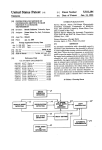
600
/
604
/
VIDEEI BUFFER
INPUT
DIGITAL
vmgu RAM
(1)
601
TV
RGB
IJUTPUT
CIRCUIT
VIDEO
DLDDUT
{610
&
f
602
GRAPHICS
TNT‘"
606
‘8’ OVERLAY
]
{612
CIRCUIT
(3)
s
_.-p 1
VGA GRAPHICS
BUFFER
MUX m
640 x 480 x 8
[608
DAC
(8)
'
funcncm "1 Predetermmed “Ems °f the v1de° buffer
.. 340/721
1024 x 512 x 1a (12) (11)
'
data
in conjunction with normal
write operations
in the
.
.
.
.
.
5,065,231 11/1991 Greaves et a1. ................... ,. 340/734
VIDED
-
video. buffer
to control
circuitry
to disable
the write
.
.
.
.
.
Pappas et a1. ..
t
0
RG3
GRAPHICS
<3)
MUNITDR
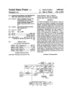
US. Patent
CGTI.‘
June 15, 1993
28
SE:_
Sheet 1 of 9
5,220,312
5328 82> :2;
82:> ESlMsEaS
32:563 °
SEE;238
1 5:;
/
8:3: 5 w
it
=52I
D_UU253'1
35:w52
5 $ 38
SE238E!
9.071
US. Patent
June 15, 1993
Sheet 2 of 9
5,220,312
ENFH.ZD
E
.w
N
5. 52
mom
QZHU wuHIm¢U
wow
I250 mwEm
A8502m9 l.2 06 5 >Al.2 06
8m
v
_
IGXE
US. Patent
June 15, 1993
Sheet 3 of 9
5,220,312
3:5 6 E52;
ME.S:
5m
252
.
l
.
l
.
-
'
.
.
.
.
I
.
-.
.
.
..
.
.
.
.
-
m.0_n
?m.ew3z:am
2 E: 32>
Q235;
U.S. Patent
June 15, 1993
Sheet 5 of 9
and-u
. P7.
.....-
..
1.l
US. Patent
June 15, 1993
Sheet 9 of 9
5,220,312
m.w_n
\\
o2J.\|I0
l
935(I.
2(:I
mg
b
L
mg
1
5,220,312
2
monitor unmodi?ed. This same method can be used to
PIXEL PROTECTION MECHANISM FOR MIXED
GRAPHICS/VIDEO DISPLAY ADAPTORS
show video “objects” in the foreground, on a graphics
background. Here, the objects (which could be rectan
gular video “windows” or arbitrarily shaped objects)
FIELD OF THE INVENTION
The present invention relates to the ?eld of computer
that are to be seen as video are drawn in the keying
color, which is some color other than that of the graph
ics background (refer to FIG. 1B). Graphics objects can
display devices. More speci?cally it is directed to inter
active display device architectures in which standard
video data and high-resolution computer generated
graphics data may each be displayed in different combi
also be shown in the foreground, provided they are not
drawn using the keying color.
nations on a high-resolution graphics monitor. The
invention provides a mechanism for preventing un
wanted data from overwriting predetermined windows
on the display.
15
CROSS REFERENCE TO RELATED
APPLICATIONS
US. patent number 4,994,912, ?led Feb. 23, 1989
of Lumelsky et al., Entitled "Audio Video
Interactive Display” discloses a video adapter architec
ture which allows the simultaneous viewing of video
and graphics data via “windowing” split images or the
like. Two frame buffers are provided, one for storing
video data and one for storing graphics. By utilizing
appropriate control architecture the outputs of both
buffers are matched to each other and to a high-resolu
tion monitor on which composite displays may be gen
erated.
FIG. 2 illustrates a typical circuit for implementing
the color keying scheme. It is comprised of a register
200 to hold the digital value of the keying color, a digi
tal comparator 202, and a fast (pixel speed) analog mul
tiplexer 204. The n-bit key register is constantly com
pared with the n-bit digital representation of the graph
ics pixels that are about to be displayed. N is typically a
number between 1 and 8 in todays graphics displays.
When one of these incoming pixels has the same value
as the key color, the output of the comparator is as
serted. This causes the analog switch 204 to output the
voltage of the video signal at that instant. For any other
color of input pixel the comparator will output the
voltage of the analog graphics signal. The circuit shown
is adequate for monochrome systems, where there is
only one color component. With color graphics sys
tems, one analog switch is necessary for each color
component (typically three-one for each of Red,
Green and Blue).
Typically, these overlay schemes are employed by
BACKGROUND OF THE INVENTION
30
dedicated, video-based application programs that con
There have been several systems in recent years such
trol external video sources such as videodisk players,
VCR’s, etc. The user would start the application, which
would in turn initialize the key register with a speci?c
tion of the infowindow product, reference should be
made to one of the following publications describing 35 color and subsequently draw the graphics screen with
the appropriate areas drawn with the keying color.
same.
as IBM’s Infowindow product that integrates graphics .
with live video on one monitor. For a detailed descrip
1) “Infowindow Guide to Operations” Order No.:
SK2T0297 and, I
2) “Infowindow Enhanced Graphics Adapter: Hard
Several problems are encountered when one con
siders windowing, i.e., non-full-screen systems. These
systems may have more than one application shown on
the screen at a given time, especially with today’s win
ware Maintenance and Service Manual" Order
No.: SK2T0298, Both are available from IBM
dowing, multitasking operating systems (e.g., the IBM
Corp. Mechanisburg, Pa.
Typically, the graphics information is “overlayed”
A first problem is encountered when the screen is
05/2 with Presentation Manager).
shared by both video-based and non-video applications.
image, with the foreground being comprised of various 45 The non-video applications typically know nothing at
on top of the video; the background is a moving video
graphic objects, such as icons, menus, or text.
In order to display both elements on a single monitor,
all about color keying, much less what color the current
key is. They draw their various objects on the screen
assuming that any color may be drawn and will be seen
on the screen unmodi?ed. As the video applications
graphics signal, so that both rasters are the same size
and are displayed at exactly the same rate. Furthermore, 50 attempt to utilize the color key, various colored graphic
objects in the non-video application will suddenly be
each video pixel should correspond one to one with a
it is necessary to synchronize the video signal with the
graphics pixel so that both types may be addressed in
replaced by video. Clearly, this is an unacceptable situa
the same manner. One way to achieve these require
tion.
ments is through the use of two separate frame buffers,
one for graphics, and one for video, as described fully in
video applications are run concurrently on one screen.
US patent application Ser. No. 4,314,623 of Lumelsky
Essentially, the multiple applications will contend for
This problem is further complicated when multiple
one resource: the color key register. When a given
and Peevers, entitled “Audio Video Interactive Dis
application is running, it may modify the key register
play”, ?led on Feb. 23, 1989, “Audio Video Interactive
Display”. The video information is read out of the dual
for its own purposes. This may cause disturbing effects
port VRAM based video buffer using the same synchro 60 in other application windows, since they may have
nization and clock signals as are used for the graphics
drawn graphic objects in the same color as the new
Frame Buffer.
keying color. When the key register is modi?ed, these
The most common method for overlaying is known
objects will suddenly appear as video objects on the
as “color keying”, where the background color for the
screen, which is almost certain to be undesirable from
graphics information is de?ned as the “keying” color, 65 the user’s standpoint.
with all pixels of that special color being replaced by
A second problem is encountered when it is desired
live video in these positions on the monitor (refer to
to use static video images on a common screen along
FIG. 1A). Pixels of all other colors are shown on the
with motion video and graphics. An example of this is
3
5,220,312
shown in FIG. 3, where a still video snapshot is placed
in a graphics window which is presented on a motion
video background. The same buffer is being viewed in
both the still video window and the moving video back
ground, i.e., video overlay is taking place in both of
5
dressing circuitry in combination with straight-forward
combinational logic to achieve the locking function.
these regions of the screen. In general, this situation
may result whenever the high-color content capabilities
The input lock mechanism utilizes a RAM which
stores the input lock pattern data and utilizes said data in
of the video buffer are desired to present quality static
conjunction with normal write operations in the video
images along with graphics while motion video is oc
curring in the background.
4
The output lock mechanism utilizes an extra bit-plane
in the video buffer which stores a predetermined “lock”
pattern and utilizes the serial output port of the buffer
operating under control of standard frame buffer ad
10 buffer to control the column address strobe (CAS) cir
cuitry to disable the write function in predetermined
regions of the video buffer.
The difficulty is that the still region must somehow be
protected from being overwritten by the surrounding
process of sampling the live video background. As the
BRIEF DESCRIPTION OF THE DRAWINGS
FIGS. 1A and 1B are diagrammatic representations
new video information is stored into successive loca
tions of the video buffer, those locations that store the
of a display monitor illustrating various “windowing”
operations possible on a monitor display which illus
trate the various types of graphic and video data which
may be combined to form a composite display which
static image will be corrupted, unless the sampling pro
cess is somehow prevented in this region.
Accordingly there is a need for a system that will
solve these problems which is effective, reasonable in
cost and, most importantly, can achieve these results in 20 illustrates the problems addressed by the present inven
tion.
mixed application systems as described above.
FIG. 2 comprises a functional diagram of a typical
prior art “color key” circuit by which graphics data
having a particular color is automatically displayed in
SUMMARY AND OBJECTS
It is a primary object of the present invention to pro
vide a mechanism, which is both cost-effective and
reliable, for preventing predetermined areas on a moni
tor screen from being overwritten by unwanted mate
25 predetermined windows based on the background color
of the graphics data.
FIG. 3 comprises an illustration of a monitor display
similar to FIGS. 1A and 1B, illustrating a further type '
rial.
of “window” presentation illustrating the function per
It is a further object of the invention to provide an 30
formed by the input lock mechanism of the present
output lock mechanism which prevents a graphics win
invention.
dow on the monitor screen from being overwritten by
FIG. 4 comprises a functional block diagram illustrat
video data.
ing how a more complex “color key” mechanism may
It is another object of the invention to provide such
be incorporated in the present invention for automati
an output lock mechanism which utilizes “color key” 35 cally allowing up to 15 different graphics windows to
controls and existing frame buffer architecture to
be automatically displayed on the monitor screen based
achieve the output lock function.
on a table driven “color key” architecture, while at the
It is another object of the invention to provide an
same time retaining the attributes of the present output
input lock mechanism which is effective to prevent a
lock mechanism.
static video window from being overwritten by motion 40 FIGS. 5A-5D are illustrative drawings similar to
video.
FIGS. 1A, 1B and FIG. 3, illustrating the types of mul
It is another object of the invention to provide such
ti-windowed mixed displays controlled by the output
an input lock mechanism which uses much of the exist
lock mechanism of the present invention.
ing frame buffer hardware to achieve the locking func
FIG. 6 comprises a high level of functional block
tion.
45 diagram illustrating the overall architecture of the pre
Other objects features and advantages of the inven
ferred embodiment of the output lock mechanism of the
tion will be apparent from the subsequent description of
the invention, the drawings and the claims.
present invention.
FIG. 7 is a diagrammatic illustration of the video
The objects of the present invention are accom
buffer memory organization showing the various drive
lines connected thereto and further illustrating the loca
tion of the input lock mechanism of the present inven
tion and its control of the column address strobes (CAS)
as well as clearly indicating that the output lock data is
plished in general by a locking mechanism which may
be readily incorporated into a high-resolution video
display system including a high-resolution monitor, a
computer for providing controls signals to said display
system and including a high-resolution frame buffer for
storing computer generated graphics images and read
read as a single bit from the output port of the buffer
55 memory separate from the video data.
ing out said graphics images at a rate controlled by said
control signals, and a video data system including a
video frame buffer which reads out video data under
control of said computer. An output locking mechanism
is functionally located between the output of both said
frame buffers and the high-resolution monitor and in
cludes means for preventing video data from overwrit
ing graphics data on said monitor screen with video
data. An input locking mechanism includes means for
preventing static video data stored in predetermined 65
regions of the video frame buffer from being continu
ally overwritten by motion TV data being continually
input to said video frame buffer.
FIGS. 8A, 8B and 8C comprise functional schematic
diagrams of the input lock circuitry shown in FIG. 7
which produce the controlling column address strobe
pulses CAS 0’ and CAS 1'.
FIG. 9 comprises a series of characteristic signal
wave forms produced by the system during operation of
' the input lock mechanism of the present invention as
shown in FIGS. 7 and 8.
DESCRIPTION OF THE DISCLOSED
EMBODIMENT
The present invention provides pixel protection
mechanisms to address these problems. The ?rst prob
5
5,220,312
lem is solved using an “Output Lock” mechanism,
whereby speci?c regions of the screen are prevented
6
video keying over window operation to take place in
that window.
An extension of the present invention is shown in
FIG. 4. If multiple bits are used in the Output Lock
from being overlayed by video keying operations, re
gardless of the color of the graphics objects in those
regions. This effectively solves the problem of running
both video and non-video applications simultaneously
memory, a more ?exible overlay scheme can be imple
on one screen. An extension to the Output Lock mecha
mented, wherein each of several active video windows
can have a dedicated overlay color independent of the
nism solves the problem of having multiple active video
applications, by allowing each to have an independent
keying color, without affecting the others. Also dis
overlay colors used by the other windows. Here, the
Output Lock memory would have, for example, four
bit entries, with each entry specifying a “window num
her” from 1 to 15. When a video window is opened, it is
closed is an efficient means for loading the Output Lock
protection mechanism.
assigned a window number and the region in the Output
Lock memory corresponding to the video window is
mechanism, whereby speci?c regions of the frame
?lled with this number. The number “0” is interpreted
buffer can be prevented from being updated by the 15 as before, i.e., no video overlay allowed. If it is desired
process of sampling live video, thus allowing static
to support more than 15 active windows, more bits must
video images to remain on a dynamic video back
be used in the Output Lock memory.
ground. An efficient means for loading the Input Lock
Referring brie?y to FIG. 4, as video pixels are being
mechanism, similar to that for loading the Output Lock
read out from the video buffer, the corresponding 4-bit
mechanism, is also disclosed. In the sections that follow,
locations of the multi-bit Output Lock memory 603
the Output Lock and Input Lock mechanisms will be
(included in the video buffer) are also read out. The
described and discussed separately.
4-bit number is used to address a l5-element “keying
Thus, to recapitulate, the input and output locks of
color” table 40. The keying color thus addressed is then
the present invention broadly function to establish
used in the color keying operation as described earlier
blocks to the presentation of incorrect data in certain 25 with reference to FIG. 2. The keying color used is
designated windows on the display screen. The former
hence dependent on the window number currently
prevents the overwriting of a static video window and
being displayed on the graphics screen. Each active
the latter prevents overwriting a graphics window.
window (up to 15 in all) therefore can de?ne its own
They are functionally located at the input to and output
keying color, without regard for the keying colors used
from the video frame buffer. In the above context a
by other application windows currently on the screen.
window is usually understood to be smaller than the
The output lock is activated to force graphics data, only
whole display screen, however, if the proper address
when OL=00O0. Otherwise when OL¢O the color key
parameters were given to the Input Lock and Output
is active and graphics data will be displayed only when
Lock mechanisms, they would be effective to control
there is a match. For a detailed explanation of the opera
the whole screen as will be apparent from the subse 35 tion of the Output Lock, reference should be made to
quent description.
the subsequent description of FIG. 6. The reference
numbers in FIG. 4 correspond to those in FIG. 6 for
Output Lock
convenience of reference.
The protection scheme implemented involves the use
There is some overhead involved in the process of
of an additional Output Lock memory means to store 40 updating the output lock memory 603 each time a
information about which regions of the screen may
graphics window is opened or closed. The window
utilize video overlay, with the other regions having
manager must'typically update each location in the
video overlay defeated. This memory has the same
Output Lock memory that is affected by the update.
The second problem is solved using an “Input Lock”
height and width as the video buffer, and contains one
This problem becomes more serious as more and more
or more bits of information corresponding to each pixel. 45 windows become active on the screen. Consider the
The basic technique requires only one bit per pixel in
the display memory. An extension to the technique
involving the use of multiple-bit entries will be de
case where there are 5 video-based windows on the
screen and a sixth graphics-only application is opened
that has a large window (shown within the dotted lines)
overlapping the other ?ve windows, as in FIG. 5A. The
scribed below. The one bit scheme is used to determine
on a pixel-by-pixel basis whether or not a given high 50 region (shown in FIG. 5B) in the Output Lock memory
resolution pixel may have the video keying operations
corresponding to the large graphics window must be
outlined above performed on it. If the bit is set, video
reset by the window manager in order to prevent video
keying operations are enabled for that pixel. If it is not
set, that pixel will be displayed from the graphics frame
overlay in that region. This requires one large-area data
buffer regardless of the color of the graphics pixel, i.e.,
the video overlay operation is defeated.
In a windowing environment supporting multiple
applications, the window manager would initially clear
move in software initializing a large area to all O’s
55
(area=window). Now, consider that this graphics win
dow is closed, producing a screen like that shown in
FIG. 5C. The previously overlapped video windows
are now uncovered, and the video overlay operation
must be re-enabled in each uncovered region. Here, the
tions altogether. When a subsequent application is 60 window manager must update the regions shown in
this memory so as to disable keying (color key) opera
started, the window manager would open a window on
the high-resolution screen for that application to display
its output. If the application doesn’t employ or support
video, nothing more needs to be done. However, if a
FIG. SD, reinitializing all ?ve regions separately. The
performance of the system may be compromised by
these update operations.
The performance degradation described can be mini
video application is started, the window manager would 65 mized if some form of hardware assistance is provided
open (draw) the application window in the graphics
to allow the window manager to quickly update the
buffer and at the same time place ones in the corre
appropriate sections of the screen. The present inven
sponding region of the Output Lock memory, enabling
tion provides such assistance with minimal additional
7
5,220,312
8
hardware expense by using the same address control
circuitry that is used to address video data regions of
ips digital T.V. chip circuit family including a 12 bit.
The frame buffer is of conventional design utilizing
the video buffer during video sampling. By using this
standard off the shelf video RAMS. All of the RAS,
address control hardware to address the output lock
memory instead of the video buffer, rectangular regions
of this memory can be loaded very rapidly (at video
CAS, data ports (in and out) address ports and registers
etc.. operate as in a standard frame buffer design com
prised of such standard video RAMS chips. The Input
Lock and Output Lock of the present invention would
rates). In the actual 0L accessing (writing) operation
the video-containing bits of each pixel would be
be connected to the conventional frame buffer architec
blocked out (protected) by any well known means
ture as disclosed herein.
(write per bit) allowing only the desired 0L bit(s) in
As will be described subsequently, the input lock
each pixel to be written. It will be appreciated by those
mechanism performs an external modi?cation to the
skilled in the art that any windowing mechanism or
method resident in the computer may be used to gener
ate the window coordinates which establish the Input
Lock and Output Lock data patterns of “l”s and “O”s.
column address strobe pulses. The output lock mecha
nism in the simplest (1 bit) embodiment disclosed
herein, utilizes an extra bit plane already existing in the
One such method is shown in previously referenced
frame buffer. The extra bit in this plane must of course
be accessed for read/write ops, however, this circuit
copending patent application Ser. No.: 314623.
Accordingly details of the operation of the lock data
capability is also present.
Accordingly, details of the operation and construc
generating mechanism is not shown as the details form
tion of the frame buffer and its support circuitry are not
no part of the present invention.
20 shown as they form no part of the present invention and
the inclusion of such detail would obfuscate same.
Input Look
The following sections describe in detail how the
The Input Lock mechanism provides an effective
Input Lock and Output Lock functions are imple
means for protecting speci?c static video regions
mented in the preferred embodiment of the invention.
through the use of a special Input Lock memory. This is 25 In this embodiment, the graphics information is pro
a one-bit memory having the same height and width as
vided by the Video Graphics Array (VGA) display
the video buffer, where the bits stored selectively con
trol whether or not corresponding pixels in the video
controller 602 (FIG. 6) that is integrated with IBM’s
PS/2 line of personal computers. See for example IBM
buffer get updated by the video sampling process.
PS/2 Model 80, Technical Reference #68X2256 avail
Where there are zeroes in this memory, corresponding 30 able from the IBM Corp. Mechanicsburg, Pa. It has a
locations in the video buffer may be updated by the
resolution of 640 pixels per scanline by 480 scanlines.
incoming live video; where there are ones, the corre
Each pixel has eight bits of data describing its color.
sponding locations in the video buffer are prevented
The video buffer 600 (FIG. 6) has the same height and
from being overwritten.
width as the graphics buffer. It should be clearly under
As was the case with the Output Lock memory out
stood that these speci?c dimensions or parameters are
lined above, there is some software overhead involved
not in any way critical to the invention and that other
in maintaining the Input Lock memory, as various static
resolutions are readily implemented (to suit other
and moving video regions are manipulated on the
graphics displays, for example) without departing from
screen. Again, hardware assistance can be provided by
the spirit and scope of the invention. In the following
ef?cient use of the video sampling address control hard 40 pages the ?rst section‘ will describe the implementation
ware. Using this hardware to address the Input Lock
and operation of the Output Lock circuitry, and the
memory allows rectangular regions to be set and reset
second will describe the same aspects of the Input Lock
very quickly (at video rates).
circuitry.
Before proceeding with a description of the embodi
The structure of the Output Lock circuitry is illus
ment, it should be noted, in general that the synchroni 45 trated in FIG. 6.
'
zation of incoming motion (or still) video data with the
There are 2 buffers in the basic system. The video
high-resolution graphics output from a host computer is
buffer 600 is comprised of 6 l-Megabit Video RAMs
normally done by using the unique dual-port properties
(e.g., Toshiba TC524256) organized to yield a 1,024 by
of VRAM technology. The secondary (serial) port of
512 by 12-bit structure. Eleven of the twelve bits are
these special-purpose VRAMs can be operated com 50 used to store motion video as it comes in from a video
pletely asynchronously to the primary (random) port.
source (not shown). The remaining bit is the Output
Hence, the primary port can be used to store incoming
video information synchronously, as it comes in, while
the secondary port can read the video data out of the
Lock bit described below. Note that only a 640x480
region of this buffer is actually used to store video; the
remainder is unused, off-screen memory. This video
frame buffer synchronously with the high-resolution
information is read out of the second serial port 601
found on all Video RAM devices, and converted to
RGB form via a Digital TV Output Circuit 604, such as
graphics display. Thus, time base correction can be
achieved by appropriate use of the independent I/O
properties of the video RAM’s two ports. The present
invention assumes the use of appropriately synchro
nized frame buffers, one for graphics data and one for
video data. The synchronization of the data out parts is,
of course, necessary for “windowing" operations as
tion of the VGA Graphics Buffer 602, refer to the IBM
well as being required for properly driving the high
Personal System/2 Technical References, such as man
that found in the Philips digital TV chip set. (See for
example the manual entitled “Digital Video Signal Pro
cessing” Philips Components, #9398 063 30011)
For detailed information on the structure and opera
resolution monitor.
ual number 68X2256. The 8-bit pixels from the Graphics
It should also be clearly understood that the circuitry 65 Buffer go to the Overlay Circuit_606 to generate the
and controls of the present invention as set forth and
described herein are intended to function in cooperation
with and require no signi?cant modi?cation of the Phil
overlay signal, and to the Palette/DAC chip 608 (Inmos
IMS-Gl7l in this disclosed embodiment). The Palette/
DAC 608 converts the 8-bit'pixels to RGB form.
9
5,220,312
The RGB MUX 612 is a 3-channel 2 to l Multiplexer
10
register 702 via the host computer data bus BPCDB,
that switches between the RGB signals from the Video
write control signal IOW-, and register address decode
LD OLDR. A normal “video sampling” operation is
Buffer 600 and those from the Graphics Buffer 602 on a
pixel-by-pixel basis, as determined by the select input
allowed to take place for one frame, after which all
which is driven by the AND gate 610. When the select
input is a logic 1, video information is sent to the RGB
monitor. When it is a 0, graphics information is dis
locations within the desired region in the Output Lock
memory 603 will have been set or reset, depending on
the contents of the register.
At the video buffer serial output port 704 the ll bit
video data output VIDDOUT and 1 bit Output Lock
played. The Output Lock mechanism is implemented by
making use of the 12th bit of the Video Buffer 600 as an
Output Lock bit, known as Output Lock Data Out
(OLDOUT). As each 11-bit video pixel is read out of
the video buffer, the corresponding Output Lock bit is
Data Output OLDOUT are shown. They are used as
shown in FIG. 6.
In order to access this bit as though it were a separate
memory, a means must be provided whereby only the
12th bit or only the ?rst 11 bits are modi?ed. During
read out as well. This bit will affect the operation of the
overlay circuit described earlier. When the bit is a one,
overlay operations take place as normal. However, if 15
normal video sampling operations, the ll video bits
the Output Lock bit is zero, the AND gate 610 will be
must be constantly updated by the incoming video in
forced to 0, forcing graphics data to be selected by the
formation, while the l2th (Output Lock) bit must be
RGB Multiplexer 612, regardless of the overlay signal.
Output Lock Flash Write
As mentioned above, it is important to improve the
performance of writing data to the Output Lock mem
ory 603. By cleverly sharing the function of the video
address generation hardware, it is possible to set and
clear rectangular portions of the Output Lock memory 25
at the same speed as video is sampled (one location
every 70 nsec). This performance is adequate for most
preserved. However, when the Output Lock memory
603 is modi?ed, only the 12th bit should be updated,
leaving the 11 video bits intact.
This can be accomplished through the use of the
“write-per-bit” capability found on most commercially
available video RAM chips. By the proper use of the
control signals to these RAM chips, it is possible to
mask out individual bits during an access, preventing
them from being modified, while the other bits get up
common windowing environments. This function re
dated normally. Hence, when video sampling opera
quires a hardware mechanism that allows the system to
tions take place, the write-per-bit function will mask the
address a rectangular array in the frame buffer in ap 30 12th bit of the frame buffer 600, preserving the Output
proximately 1/30 of a second. A mechanism for doing
Lock information. Conversely, when the output lock
this is disclosed in detail in previously referenced co
memory 603 is accessed, write-per-bit is used to allow
pending US. patent application #314623.
only the 12th bit to be modi?ed, preserving the 11 bits
A simpli?ed block diagram of the video buffer mem
ory organization can be seen in FIG. 7.
Before proceeding with a description of this ?gure,
reference should be made to the following table in
which various abbreviations used in the ?gure are de
?ned.
of video information.
35
Input Look
The Input Lock circuit 706 in FIG. 7 is shown in
detail FIGS. 8A, B and C with a timing diagram there
for in FIG. 9.
Before proceeding with a description of FIG. 8, ref
erence should be made to the following table in which
various abbreviations used in the ?gure are defined.
BPCDB - Buffered PC Data Bus
LDOLDR - Load Output Lock Data Register
10W - I/O Write Strobe
CASG
CAS 1
CAS 01
CAS 11
OLDIN
-
Column Address Strobe (Block 0)
Column Address Strobe (Block 1)
CAS a’ Modi?ed CAS w
CAS l'Modi?ed CAS 1’ Modi?ed CAS 1
Output Lock Data Input
45
HS -
CAS 1 -
VIDDIN - Video Data Input
FBADDR
RAS
CAS
DAT
ADDR
-
Frame Buffer Address
Row Address Strobe
Column Address Strobe
Frame Buffer Data
Frame Buffer Address
CAS 0 -
INLK D OUT -
BPCDB -
IOW ~
50
LDILCR -
SAMPLE/PC -
Column Address Strobe 6
Input Lock Data Out
Horizontal Sync
Column Address Strobe 1
Buffered PC Data Bus
I/O Write Strobe
Load Input Lock Control Register
Sample Video/Load from PC
FB ADDR - Frame Buffer Address
INLKDIN - Input-Lock Data Input
- Row Address Strobe
The buffer 600 is 12 bits deep, with 11 bits used for
video (7 luminance, 4 chrominance), and 1 bit for Out
put Lock information. This simple list plane of Output
lock memory is designated in the ?gure by the reference
numeral 603. Hence, the same addressing circuitry used
for rapid (real-time) sampling of video into the frame
buffer can be used to quickly load rectangular regions in 60
this “12th bit” or Output Lock memory 603.
The Output Lock Data Input (OLDIN) register 702
Input Lock Write Enable
D: Flip-Hop Data Input
C: Flip~Flop Clock Input
RD: Flip-Flop Reset Direct Input
CE: Flip'Flop Clock Enable Input
W: RAM Write Enable
Flash Write Input Lock Write Enable
PC Input Lock Write Enable
Input Lock Data Output
- Input Lock Flip-Flop 0 output
Input Lock Flip-Flop 1 output
is wired directly to the 12th data bit of the frame buffer
600, while the other 11 bits are connected to the 11-bit
It consists of a 256K><1 dynamic RAM 800 (e.g., T.I.
video data input bus (V IDDIN). To quickly load a 65 TMS4256), and associated control logic. There are 3
rectangular region in the Output Lock memory 603, the
basic sections in the circuit. The bottom portion 8C is
sample addressing circuitry is ?rst set up to access the
the Input Lock memory itself (INLKMEM). The mid
desired region and a O or 1 is written to the OLDIN
dle portion FIG. 8B is used when loading the Input
11
5,220,312
Lock memory, and the upper portion FIG. 8A is used
when the memory is accessed, i.e., during video sam
12
tively. The output of the second flip-?op 804 is then
used to determine whether the next two pixels will be
pling operations.
protected or not. This protection is done by OR’ing the
2nd ?ip-?op with the CAS timing pulses CASO- and
CASI- in OR circuits 806 and 808 before they go to the
frame buffer. If the 2nd ?ip-?op 804 (INLKl) is 0, then
The address to the dynamic RAM 800 is the same
address as the one applied to the frame buffer 600
(FBADDR) in FIG. 7. Since the same address is used,
the content of the Input Lock memory can be thought
of as another “layer” behind the frame buffer pixels,
mapping each pixel. This is conceptionally the same as
for the OL memory plane. Therefore, as will be appre
ciated by those skilled in the art, the same hardware that
is used to address rectangular regions of the video
buffer, 600 is used to address rectangular regions in the
Input Lock Memory 800. Since the DRAM is 512x 512
(256K), each location affects 2 consecutive samples in
the next two samples will not be written into the frame
buffer 700, since the CAS timing pulses CASO- and
CASl- will not get through the ?nal OR gates, and
without a CAS pulse, data cannot be written. If the 2nd
?ip-?op (INLKI) is 1, then the next two samples will be
written. Horizontal Sync (HS-, active low) is inverted
to produce signal HS, which in turn is used to clear both
?ip-?ops 802 and 804 at the beginning of each scan line
using their Reset Direct (RD) inputs.
the 1024x512 frame buffer array 600, one in Bank 0
controlled by CAS 0 and one in Bank 1 controlled by
CAS 1.
Referring to FIG. 7, the signals CAS 0’ - and CAS 1’
- are separate CAS- signals to each of two banks (0 and 20
FIG. 9 is an example illustrating the timing of this
circuit. In this example, the sequence of bits from the
will resume, with the new Input Lock memory contents
CAS1-' and data is written.
Input Lock memory 800 is assumed to be 0,1,0, . . . so
that the 1st and 3rd sample will be written, and the 2nd
will be protected. This sequence will be repeated for
l) of the video buffer 700. Two banks are required in
each scan line, with Input Lock memory 800 determin
order to realize a 1K wide memory using memory chips
ing the particular pattern of 1's and O’s each time. At the
which are organized as 512x 512. These two signals are
beginning of a scan line, Horizontal Sync (HS-) will go
produced by the Input Lock circuit 706 in response to
active low, resetting INLKO and ILNKI once. Some
the CAS- timing pulses CAS 0- and CAS 1- which are 25 time later, in interval 1, the ?rst 0 is read out from the
in turn produced by a generic memory controller.
Input Lock memory 800 on INLKDOUT. Halfway
When the CAS pulses are passed through the Input
through that interval, this 0 is clocked into the ?rst
Lock circuit and appropriately modi?ed (or not), nor
?ip-?op 802 (INLKO). At the beginning of. interval 2,
mal memory cycles take place. When they are blocked
this 0 is clocked into the second ?ip-?op 804(INLK1).
through the action of the Input Lock memory, the
Since INLKl is 1, the CASO- and CASl- pulses are
memory cycles will be prevented or inhibited.
allowed through OR gates 806 and 808 to produce
FIGS. 8 A-C illustrate the implementation of the
pulses CASO -’ and CAS1-’, thus writing data into the
Input Lock controls. To load the Input Lock memory,
frame buffer 600. Also in interval 2, the next data is read
a static value (0 or 1) is placed in the Input Lock Data
out on INLKDOUT, which is now a 1. This gets
Input Register 810 (INLKDIN) (input D of the INL 35 clocked through ?ip-?ops 802 and 804 in the second
KMEM 800) by the host computer via the host com
half of interval 2 and the beginning of interval 3 respec
puter data bus BPCDB, write control signal IOW-, and
tively. At this point, INLKl is low, which prevents
address decode LDILCR. This value will be written
CASO- and CASl- from getting through OR gates 806
into a rectangular region of the input lock memory 800.
and 808 so CASO-' and CAS1-’ stay high (inactive).
As addressed by the current sampling operation, when
Therefore, no data is written. Again, the next data
the Flash Write Input Lock Write Enable register 812
comes out on INLKDOUT in the same interval (3).
(FWILWE) is reset to 0. Once the desired region is
This time, it is another 0, so that in interval 4, CASO
loaded, INLKFWE is set to 1, and normal operation
and CASl- are allowed to pass through on CASO-' and
preserved.
The Input Lock memory 800 can also be loaded di
rectly by the host computer by resetting the PC Input
Lock Write Enable (PCILWE) register 814. In this
case, an arbitrarily shaped region in the Input Lock
45
CONCLUSIONS
The system herein described has many of its func
tional characteristics generalized to accommodate fu
ture improvements in mixed digital television/personal
memory 800 can be loaded, as the host computer drives 50 computer graphics display technologies without depart
FBADDR directly. When the host computer accesses
ing from the spirit and scope of the invention. In this
the video buffer 600 in this way, the mode signal Sam
ple/PC- will be low, selecting PCILWE- to drive the
?nal Input Lock Write Enable signal INLKWE- (via
multiplexer 816).
Typically, the Input Lock memory 800 would ?rst be
cleared (set INLKDIN to 0 and set up the sample ad
dressing to address the full memory) and then a small
region would be set (set INLKDIN to l and set up
sample addressing to address the desired sub-region).
In operation, Input Lock Data Output bits (INLK
embodiment, the digital television subsystem is based on
a chip set manufactured by Philips as stated previously.
The host system is illustrated as an IBM Personal Sys
55 tem/2 with MCA, which includes a VGA graphics
(640x480X4 bit pixel) subsystem. The high-resolution
video system described need not be limited to the band
width and bits/pixel provided by the VGA. Future
digital TV and graphics technologies can readily be
incorporated without departing from the spirit of this
invention.
It is accordingly not intended to limit the present
invention to the speci?c embodiments described above.
It is recognized that many changes may be made in the
modify the CAS- signals before they are applied to the 65 circuits and processes speci?cally described herein
video buffer 600.
without departing from the scope and teaching of the
The INLKDOUT data is passed through 2 flip-flops
present invention, and it is intended to encompass all
802 and 804, clocked by CASO- and CASl- respec
other embodiments, alternatives, and modi?cations con
DOUT) are read out of the Input Lock memory 800 one
at a time, as video sampling takes place. The INLK
DOUT data is then used by the circuit in FIG. 8A to
5,220,312
l3
14
sistent with the invention as set forth in the appended
claims.
We claim:
entering predetermined patterns of ones and zeroes
the video data to be displayed on the monitor when
there is a match, and
an input locking mechanism including means for se
lecting one of two lock modes the ?rst mode for
currently address predetermined regions of said
provided, by a host computer at addresses provided .
by said host computer and
1. In a high-resolution video display system including
means for inhibiting the writing of any data into pixel
a high-resolution monitor, a computer for providing 5
data storage locations of said memory while said
control signals to said display system, a high-resolution
output lock data is being stored therein.
graphics frame buffer for storing computer generated
3. A high-resolution video display system as set forth
graphics images and supplying said graphics data im
in claim 1, wherein said input lock memory comprises a
ages to the monitor at a rate controlled by said com
dynamic random access memory (DRAM) having as
puter generated control signals, and a video data system
many bit storage locations as there are pixels in the
including a video frame buffer for supplying video data
video frame buffer for storing input lock pattern data
to the monitor under control of said computer the im
and
provement which comprises,
means for utilizing ‘said input lock pattern data in
an output locking mechanism functionally located
conjunction with normal write operations in the
between the output of both said frame buffers and
video frame buffer to control the addressing and
the high-resolution monitor including combinato
accessing circuitry of the video frame buffer to
rial and switching circuit means for allowing
disable
the accessing function in predetermined
graphics data to overwrite video data 1) under
regions thereof, and
control of a bit pattern stored in an output lock
means for accessing by a host computer for loading
memory having a bit set to a predetermined state 20
said DRAM with an input lock data pattern indica
for every pixel of graphics data to be displayed or
tive
of the region on the monitor on which moving
2) under control of a color key circuit including
video data is not to be displayed,
means for comparing a predetermined color key
said means for loading comprising utilizing the ad
?eld associated with each graphics data pixel with
dressing circuitry of the video frame buffer to con
a color key provided by the computer and causing 25
DRAM to store said input lock data patterns in said
predetermined regions thereof.
4. A high-resolution video display system as set forth
preventing static video data stored in predeter 30 in claim 2 wherein said output lock memory further
includes a plurality of reserved bit planes in the video
mined regions of the video frame buffer as de?ned
by an input lock pattern from being overwritten by ~ frame buffer wherein a predetermined bit pattern repre
sents said output lock function and other bit patterns
motion TV data being continually input to said
video frame buffer and the second mode for pre
represent “color key”,
venting data written into said video frame buffer by 35
enabling means operable when there is no output lock
active for utilizing said color key to control graph
ics data display and
means for utilizing said color key for enabling the
display of selected video data rather than graphics
data at those pixel locations for which the color of
the graphics data matches the “color key”.
5. A high-resolution video display system as set forth
in claim 4 wherein said means utilizing said “color key
the computer from being overwritten by such mo
tion TV data,
said input lock mechanism means including input lock
memory means for storing a pattern of those bit
locations in ‘the video frame buffer which are pro
tected and
means for automatically causing the input lock mem
ory to be loaded concurrently with the writing of
.
” includes a comparator circuit for continuously com
data into said video frame buffer by a single com
mand from the computer,
45 paring the color signal accompanying graphics pixel
data with a predetermined color key, a successful com
' 2. A high-resolution video display system as set forth
pare enabling a "video output” of a multiplexer circuit
in claim 1 wherein
means which selectively functions to pass graphics data
said output lock memory comprises at least one re
or video data whereby said video data will be displayed
served bit-plane in the video frame buffer which
stored a predetermined output lock pattern and 50 on the monitor screen when said multiplexer is so en
further including
abled,
said means utilizing said "color key" bit patterns
stored in the reserved bit planes of said output lock
means for utilizing the serial output port of the video
frame buffer operating under control of the video
frame buffer addressing circuitry operating in the
monitor display mode for accessing the output lock
bit ?eld of the video frame buffer in parallel with
the video data bit ?eld,
,.
,
said combinatorial and switching circuit means in
cluding means for determining if the bit pattern in
the output lock memory represents an "output
lock" and if so disabling the output 'of the video
frame buffer and enabling the output of the graph
ics frame buffer on the data path to the monitor,
, memory further including means for utilizing said
55
color key'bit pattern to access a color key table
where an expanded color key is stored, and
further means operable under control of said output
lock pattern to enable the graphics output of said
multiplexer irrespective of the output of said “color
key” comparator circuitry.
6. In a high-resolution video display system including
a high-resolution monitor, a computer for providing
control signals to said display system, a high-resolution
and
graphics frame buffer for storing computer generated
means for loading a predetermined lock pattern into 65 graphics images and supplying said graphics data im
said output lock memory including.
means utilizing the addressing and memory accessing
controls of the video frame buffer for sequentially
ages to the monitor at a rate controlled by said com
puter generated control signals. and a video data system
including a video frame buffer for supplying video data
15
5,220,312~
to the monitor under control of said computer the im
16
means utilizing the serial output port of the video
frame buffer operating under control of the video
provement which comprises,
an output locking mechanism-functionally located
’ between the output of both said frame buffers and
the high-resolution monitor including means for 5
frame buffer addressing circuitry operating in the
monitor display mode for accessing the output lock
bit ?eld of the video frame buffer in parallel with
allowing graphics data to overwrite video data 1)
under control of a bit pattern stored in an output
lock memory having a bit set to a predetermined
state for every pixel of graphics data to be displayed or 2) under control of a color key circuit 10
the video data bit ?eld,
.
a combinatorial and switching circuit means includ
ing means for determining if the bit pattern in the
including means for comparing a predetermined
color key ?eld associated with each graphics data
pixel with a color key provided by the computer
and causing the video data to be displayed on the
monitor when there is a match;
15
said output lock memory comprising a plurality of
reserved bit-planes in the video frame buffer
wherein apredetermined bit pattern represents said
output lock function and other bit patterns repre-
buffer and enabling the output of the graphics
frame buffer on the data path to the monitor, and
enabling means operable when there is no output lock
active for utilizing said bit pattern for accessing a
color key to control graphics data display and
means utilizing said color key for enabling the display
of selected video data rather than graphics data at
those pixel locations for which the color of the
graphics data matches the "color key”.
sent color keys;
20
output lock memory represents an “output lock”
and if so disabling the output of the video frame
'
"
'
'
'
25
30
35
45
50
55
65
‘