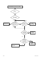
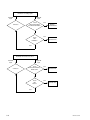
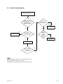
1
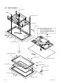
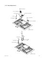
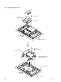
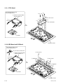
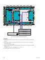
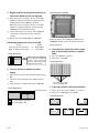
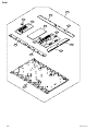
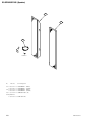
FLAT PANEL DISPLAY
PFM-42X1
PFM-42X1N
COMPONENT/RGB ACTIVE THROUGH ADAPTOR
BKM-V12
SPEAKER SYSTEM
SS-SP20B
SS-SP20S
REMOTE COMMANDER
RM-971
SERVICE MANUAL
1st Edition
! WARNING
This manual is intended for qualified service personnel only.
To reduce the risk of electric shock, fire or injury, do not perform any servicing other than that
contained in the operating instructions unless you are qualified to do so. Refer all servicing to
qualified service personnel.
! WARNUNG
Die Anleitung ist nur für qualifiziertes Fachpersonal bestimmt.
Alle Wartungsarbeiten dürfen nur von qualifiziertem Fachpersonal ausgeführt werden. Um die
Gefahr eines elektrischen Schlages, Feuergefahr und Verletzungen zu vermeiden, sind bei
Wartungsarbeiten strikt die Angaben in der Anleitung zu befolgen. Andere als die angegeben
Wartungsarbeiten dürfen nur von Personen ausgeführt werden, die eine spezielle Befähigung
dazu besitzen.
! AVERTISSEMENT
Ce manual est destiné uniquement aux personnes compétentes en charge de l’entretien. Afin
de réduire les risques de décharge électrique, d’incendie ou de blessure n’effectuer que les
réparations indiquées dans le mode d’emploi à moins d’être qualifié pour en effectuer d’autres.
Pour toute réparation faire appel à une personne compétente uniquement.
PFM-42X1/42X1N
CAUTION
ADVARSEL
Danger of explosion if battery is incorrectly replaced.
Lithiumbatteri - Eksplosjonsfare.
Ved utskifting benyttes kun batteri som
anbefalt av apparatfabrikanten.
Brukt batteri returneres
apparatleverandøren.
Replace only with the same or equivalent type
recommended by the manufacturer.
Dispose of used batteries according to the
manufacturer’s instructions.
VARNING
Vorsicht!
Explosionsgefahr bei unsachgemäßem Austausch
der Batterie.
Ersatz nur durch denselben oder einen vom
Hersteller empfohlenen ähnlichen Typ. Entsorgung
gebrauchter Batterien nach Angaben des
Herstellers.
Explosionsfara vid felaktigt batteribyte.
Använd samma batterityp eller en likvärdig typ
som rekommenderas av apparattillverkaren.
Kassera använt batteri enligt gällande
föreskrifter.
VAROITUS
ATTENTION
Il y a danger d’explosion s’il y a remplacement
incorrect de la batterie.
Paristo voi räjähtää jos se on virheellisesti
asennettu.
Vaihda paristo ainoastaan laitevalmistajan
suosittelemaan tyyppiin.
Hävitä käytetty paristo valmistajan ohjeiden
mukaisesti.
Remplacer uniquement avec une batterie du même
type ou d’un type équivalent recommandé par le
constructeur.
Mettre au rebut les batteries usagées conformément
aux instructions du fabricant.
ADVARSEL!
Lithiumbatteri-Eksplosionsfare ved fejlagtig
håndtering.
Udskiftning må kun ske med batteri
af samme fabrikat og type.
Levér det brugte batteri tilbage til leverandøren.
PFM-42X1/42X1N
1 (P)
For the customers in the Netherlands
Voor de klanten in Nederland
Hoe u de batterijen moet verwijderen, leest u in de tekst
van deze handleiding.
Gooi de batterij niet weg maar lever deze in als klein
chemisch afval (KCA).
Für Kunden in Deutschland
Entsorgungshinweis: Bitte werfen Sie nur entladene
Batterien in die Sammelboxen beim Handel oder den
Kommunen. Entladen sind Batterien in der Regel dann,
wenn das Gerät abschaltet und signalisiert “Batterie
leer” oder nach längerer Gebrauchsdauer der Batterien
“nicht mehr einwandfrei funktioniert”. Um
sicherzugehen, kleben Sie die Batteriepole z.B. mit
einem Klebestreifen ab oder geben Sie die Batterien
einzeln in einen Plastikbeutel.
2 (P)
PFM-42X1/42X1N
Table of Contents
1. Service Overview
1-1.
1-2.
1-3.
1-4.
Appearance Figure ...................................................................................... 1-1
Board Locations .......................................................................................... 1-1
Disassembly ................................................................................................ 1-2
1-3-1. BKM-V10 .................................................................................. 1-4
1-3-2. Rear Cover Assembly ................................................................ 1-4
1-3-3. Bezel Assembly 1 ....................................................................... 1-5
1-3-4. Bezel Assembly 2 ....................................................................... 1-6
1-3-5. Plasma Display Panel 1 .............................................................. 1-7
1-3-6. Plasma Display Panel 2 .............................................................. 1-8
1-3-7. Litium Battery ............................................................................ 1-9
1-3-8. A Board ...................................................................................... 1-9
1-3-9. CTRL Board ............................................................................. 1-10
1-3-10. XRB Board and XLB Board .................................................... 1-10
1-3-11. XRT Board and XLT Board ..................................................... 1-11
1-3-12. YDB Board and YDT Board .................................................... 1-12
1-3-13. Z-SUS Board ............................................................................ 1-12
1-3-14. Y-SUS Board ........................................................................... 1-13
Warning on Power Connection ................................................................. 1-13
2. Electrical Adjustment
2-1.
2-2.
2-3.
2-4.
PFM-42X1/42X1N
Setup Adjustment ........................................................................................ 2-1
White Balance Adjustment ......................................................................... 2-1
2-2-1. Initialization ............................................................................... 2-1
2-2-2. AD Calibration ........................................................................... 2-1
2-2-3. White Balance Adjustment ........................................................ 2-2
2-2-4. Shipment Condition Setting ....................................................... 2-2
Panel Adjustment ........................................................................................ 2-3
2-3-1. Application Object ..................................................................... 2-3
2-3-2. Notes .......................................................................................... 2-3
2-3-3. Adjustment Items ....................................................................... 2-3
2-3-4. Adjusting the Board Group (Applying the Tools) ..................... 2-3
2-3-5. Adjustment after Assembling (PDP Module Adjustment) ......... 2-4
Troubleshooting .......................................................................................... 2-7
2-4-1. Checking for No Picture ............................................................. 2-7
2-4-2. Hitch Diagnosis Based on the Display Condition ...................... 2-9
2-4-3. Checking for Component Damage ........................................... 2-12
1
3. Troubleshooting Guide
3-1.
3-2.
3-3.
Out of Order on Power ................................................................................ 3-1
No Raster State ............................................................................................ 3-3
Sound Troubleshooting ............................................................................... 3-7
4. Spare Parts
4-1.
4-2.
2
Notes on Repair Parts .................................................................................. 4-1
Exploded Views .......................................................................................... 4-2
PFM-42X1/42X1N
Section 1
Service Overview
1-1. Appearance Figure
1-2. Board Locations
TEMP
H2 (User control)
G (Power)
DDC CI
T (R) (SP)
XRT
CTRL
T (L) (SP)
L (Audio)
BKM-V10
XLT
Z-SUS
H1 (SW)
A (Main)
YDT
XRB
YDB
XLB
Y-SUS
PFM-42X1/42X1N
1-1
1-3. Disassembly
1-3-1. BKM-V10
1-3-2. Rear Cover Assembly
A
1-3-3. Bezel Assembly 1
Upper
Side
Upper
Side
1-3-5. Plasma Display Panel 1
1-3-4. Bezel Assembly 2
Upper
Side
Upper
Side
Upper
Side
Upper
Side
1-3-6. Plasma Display Panel 2
Upper
Side
1-2
Upper
Side
Upper
Side
PFM-42X1/42X1N
1-3-11. XRT Board and XLT Board
A
1-3-7. Lithium Battery
Upper
Side
Upper
Side
1-3-12. YDB Board and YDT Board
1-3-8. A Board
Upper
Side
1-3-14. Y-SUS Board
Upper
Side
Upper
Side
For removal procedure, refer to
"Plasma Display Panel 1.2".
1-3-10. XRB Board and XLB Board
1-3-13. Z -SUS Board
For removal procedure, refer to
"Plasma Display Panel 2".
Upper
Side
1-3-9. CTRL Board
Upper
Side
PFM-42X1/42X1N
Upper
Side
1-3
1-3-1. BKM-V10
CN7
A (Main) board
2 BKM-V10
1 Loosen the two screws.
1-3-2. Rear Cover Assembly
2 Four hooks
1 Four screws
4 Fourteen screws
3 Ten screws
5 Rear cover assembly
Upper
Side
Conductive cushion
1-4
PFM-42X1/42X1N
1-3-3. Bezel Assembly 1
2 Peel off the four tapes.
Upper
Side
1 Peel off the four tapes.
Conductive cushion
5 Three screws
6 T board (R),
Two brackets
CN1302
7 Four screws
3 Two screws
8 Two brackets
9 Two screws
CN1304
4 T board (L),
Two brackets
P501
0 Temp board
CN1101
Upper
Side
Conductive cushion
!- Multi button,
H2 board, Bracket
PFM-42X1/42X1N
1-5
1-3-4. Bezel Assembly 2
2 Screw
1 Four
screws
3 Four screws
4 Connector
Note : When removing the main chassis,
be sure that the two persons or
more must work together for removal.
Place the removed main chassis on the
conductive cushion.
Upper
Side
H1 board
CN201
5 Main chassis
Bezel assembly, etc.
Conductive cushion
7 Frame front assembly
Upper
Side
6 Nine screws
Conductive cushion
0 Screw
!= Filter glass
!- Power button
8 Two screws
9 H1 board
![ Bezel assembly
Upper
Side
Conductive cushion
1-6
PFM-42X1/42X1N
1-3-5. Plasma Display Panel 1
7 Two screws
8 D.C. fan, Bracket
6 AC inlet, AC socket cover
5 Three screws
P501
3 Screw
1 Two screws
4 Temp board
2 D.C. fan, Bracket
CN800
Upper
Side
Conductive cushion
CN302
CN303
CN301
!- Four screws
CN901
!= L (Audio)
board
9 Two screws
0 DDC CI board
Upper
Side
Conductive cushion
PFM-42X1/42X1N
1-7
1-3-6. Plasma Display Panel 2
CN801
CN803
CN802
CN808
CN806
CN807
1 Eight screws
2 Holder
3 G board
Upper
Side
Conductive cushion
4 Two screws
6 Four screws
5 Four screws
7 A board, Two frame module
metal assemblies, etc.
P9
8 Plasma display panel
Upper
Side
Conductive cushion
1-8
PFM-42X1/42X1N
1-3-7. Litium Battery
1 Four screws
Lithium battery removal
3 Four screws
2 Two fans and brackets
Lithium battery
(CR2032)
4 Shield
Battery holder
Remove the lithium battery in the
direction of arrow.
5 Lithium battery
Upper
Side
Conductive cushion
1-3-8. A Board
CN2
CN5
CN9
1 Seven screws
CN1
CN8
CN23
CN19
CN3
CN22
3 Shield
CN501
3 A board
2 Six hexagon
screws
Upper
Side
Conductive cushion
PFM-42X1/42X1N
1-9
1-3-9. CTRL Board
For removal procedure, refer to
"Plasma Display Panel 2".
P2
P300
P201
2 A board, Two frame module
metal assemblies, etc.
P106
P102
3 Five screws
P105
P103
4 CTRL board
P200
1 G board
Upper
Side
Conductive cushion
1-3-10. XRB Board and XLB Board
For removal procedure, refer to
"Plasma Display Panel 1.2".
1 AC inlet, AC socket cover
4 Three screws
3 A board, Two frame module
metal assemblies, etc.
5 XRB board
P750
P720
P710
6 Three screws
P730
P740
P510
P700
P520
P530
7 XLB board
P540
P550
2 G board
Upper
Side
Conductive cushion
1-10
PFM-42X1/42X1N
1-3-11. XRT Board and XLT Board
1 Nine screws
Conductive cushion
Upper
Side
0 Remove the XLT board
in the direction of the arrow B.
G board
5 Two screws
9 Three screws
6 Temp board
P100
7 Multi button,
H2 board, Bracket
P140
P150
P130
P120
A
XLT Board
P110
B
Upper
Side
XRT Board
8 Open the G board in the
direction of the arrow A.
3 Three screws
P350
P340
P330
P320
Conductive cushion
4 Remove the XRT board
in the direction of the arrow B.
P310
P300
B
A
Upper
Side
Conductive cushion
2 Open the G board in the
direction of the arrow A.
PFM-42X1/42X1N
1-11
1-3-12. YDB Board and YDT Board
3 Two screws
5 Screw
4 D.C. fan,
Fan Bracket
A
9 Two screws
B
0 Remove the YDT board
in the direction of the arrow B.
P19
P18
Conductive cushion
P20
6 Remove the YDB board
in the direction of the arrow A.
P28
P27
P26
P25
P23
P24
P15
P21
P22
1 Two screws
P5
Upper
Side
2 T board (L),
Two brackets
P4
7 Two screws
8 Bracket
1-3-13. Z-SUS Board
3 Three screws
4 T board (R),
Two brackets
1 Two screws
5 Five screws
P1
2 Bracket
P4
P5
P3
P2
6 Z-SUS board
P6
Upper
Side
Conductive cushion
1-12
PFM-42X1/42X1N
1-3-14. Y-SUS Board
P5
P2
1 Five screws
P3
2 Y-SUS board
P1
Conductive cushion
Upper
Side
1-4. Warning on Power Connection
Use the proper power cord for your local power supply.
PFM-42X1 series
United State, Canada
Continental Europe
United Kingdom, Ireland, Austria,
New Zealand
Japan
Plug type
VM0233
COX-07
636
_ a)
VM1296
Female end
VM0089
COX-02
VM0310B
VM0303B
VM1313
Cord type
SVT
H05VV-F
CEE (13) 53rd (O, C)
HVCTF
Minimum cord set rating
10A/125V
10A/250V
10A/250V
10A/125V
Safety approval
UL/CSA
VDE
VDE
DENAN-HO
a) Note : Use an appropriate rating plug which complies with local regulations.
PFM-42X1/42X1N
1-13
Section 2
Electrical Adjustment
2-1. Setup Adjustment
. Required equipments
Remote commander (RM-971)
Digital voltmeter
Luminance meter : Minolta CA-110 or equivalent
If Minolta CA-110 or equivalent is
not available, make adjustment by
comparing the monitor with the
reference LCD monitor that has
already been calibrated correctly.
Signal generator : VG-854 or equivalent
. Preparation of the luminance meter
Place the light receptor block of the luminance meter
about 50 cm away from the monitor screen as shown.
3) Place the luminance meter (e.g. CA-110) 50 cm away
from the monitor. Align it with the vertical center of
the display, and adjust the focus to the optimum level
by using an eyepiece.
4) Place the monitor and the luminance meter (e.g. CA110) in a light-shielded room for adjustment.
5) Set up [SERVICE MODE] of the monitor.
3. Operation
For quick setup, set the data manually. Set Brightness,
Contrast, and Backlight to 50, 70, and 100 respectively.
Then, set the color temperature by adjusting its default
value.
4. Warm up time
Warm up for 30 minutes or more before performing any
adjustment.
1. How to enter the service mode
Luminance meter
about 50 cm
Monitor
2-2. White Balance Adjustment
2-2-1. Initialization
1) Turn on the power.
2) Input Enter → 1 → 8 → 2 from the remote controller
in this order to display SERVICE MODE OSD.
3) Select INITIALIZATION menu, and execute FILL
0xFF.
(When the initialization is completed, the power turns
off and restarts automatically.)
n
W/B readjustment is required after the panel, board or
microprocessor is replaced. However, before W/B adjustment, be sure to perform aging for more than 30 minutes
after RGB reset.
2. Setup
1) Set the timing and pattern data for the signal generator
according to the Sony timing specifications.
2) Connect the monitor video cable to the signal generator.
PFM-42X1/42X1N
1) Input Enter → 1 → 8 → 2 from the remote controller
in this order to display SERVICE MODE OSD.
2) Select INITIALIZATION menu and, execute FILL
0xFF. (When the initialization is completed, the power
turns off and restarts automatically.)
2-2-2. AD Calibration
Execute Auto Calibration as follows by using a PC (1024
x 768 60 Hz) signal.
1. PC signal
1) Display SERVICE MODE OSD and select the AD
CALIBRATION menu.
2) Input Full Black (no video) pattern.
3) Execute PC. CUTOFF.
4) Input Full White pattern.
5) Execute PC.GAIN.
2-1
2-2-3. White Balance Adjustment
After aging the unit about 30 minutes, adjust the color
matrix of each one of the color temperatures of 11000 K,
9300 K, and 6500 K as follows.
1. Preparation of adjustment
1) Equipment : Signal generator (e.g. : VG-854), luminance meter (e.g. : CA-110)
2) Signals type : If a detailed timing is needed, refer to
Sony Timing Specifications.
PC XGA (1024 x 768 60 Hz)
1080I (Y/Pb/Pr)
480P (Y/Pb/Pr)
NTSC Composite
PAL Composite
480I (NTSC Composite)
575I (PAL Composite)
3) Signal level : 700 mVpp
4) Signal pattern : Full White, 16-step gray pattern
4) Adjust the color matrix by changing the values of GGAIN and B-GAIN. (Refer to SONY Color Matrix
Specifications)
11000 K : x=276 (± 15), y=282 (± 15)
9300 K : x=283 (± 15), y=298 (± 15)
6500 K : x=313 (± 15), y=329 (± 15)
5) Adjust each of the color temperatures of 11000 K,
9300 K, and 6500 K by repeating steps 3) and 4).
2-2-4. Shipment Condition Setting
Set the shipment condition (Refer to SONY Color Matrix
Specifications.).
1) Display the SERVICE MODE OSD menu.
2) Select the FOR TEST menu, and execute INIT
GOODS.
(When INIT GOODS is completed, the power turns
off and restarts automatically.)
2. Color matrix adjustment
Execute the following programs in the following sequence
: PC → 1080i → 480p → 480i → 575i → NTSC Composite → PAL Composite.
1) After inputting each signal, adjust Sub-Offset.
. Input 16-step gray pattern.
. Display SERVICE MODE OSD and select the
WHITE BALANCE menu.
. Change Sub-Offset, and adjust the brightness of the
second step of the 16 steps of gray to be 0.5 cm/m2
or less.
(Sub-Offset : ± 0.1)
2) Input Full White pattern.
3) Set the values of R-GAIN and R/G/B-OFFSET in the
WHITE BALANCE menu as shown in the following
figure.
PC
1080I 480P
480I
575I
NTSC PAL
R-GAIN
33
34
34
34
34
34
34
R-OFFSET
61
51
51
52
51
57
53
G-OFFSET
60
53
52
52
52
62
57
B-OFFSET
63
52
51
52
51
60
55
2-2
PFM-42X1/42X1N
2-3. Panel Adjustment
2-3-3. Adjustment Items
2-3-1. Application Object
1.
1)
2)
3)
This standard is applied to the PDP42X1##7# PDP
Module, which is manufactured by the manufacturing team
of PDP promotion department or elsewhere.
2-3-2. Notes
1) Without any special indication, the module should be
at the preliminary condition more than 10 minutes
before adjustment.
. Service signal : 100% Full White signal
. Service DC voltage : Vcc : 5 V, Va : 65 V, Vs : 190 V
. DC/DC Pack voltage : V1st : 115 V, Vscw : 110 V,
_Vy : _175 V, Vzb=105 V
. Preliminary environment : Temperature (25 ± 5dC),
relative humidity (65 ± 10%)
2) After assembling the module, perform aging under the
following conditions for stabilizing its operation before
starting the adjustment.
. Service signal : 100% Full White, Red, Green, Blue
pattern signals (Service time of each pattern : within
5 minutes/cycle)
. Service DC voltage : Match the voltage with the
setup voltage at the first adjustment.
. Aging period : 4 hours or more
. Aging environment : Temperature (60 ± 2dC),
relative humidity 75% or less
3) Module adjustment should be performed in the
following sequence.
. Set the initial voltage and adjust the voltage waveform of Vsetup.
. Measure the margin of the Vs voltage and determine
the voltage.
. Adjust and check the voltage of DC/DC pack (V1st,
Vsc, _Vy, _Vzb).
. Adjust the voltage waveform of Vset-down.
. Measure the margin of the Vset-up voltage and
determine the voltage.
. Adjust the waveform of the final voltage. The
adjustment value above may vary depending on
individual units.
4) Without any special indication, adjust the module
under the ambient temperature of 25 ± 5dC and the
relative humidity of 65 ± 10%.
c
If you leave the still image displayed for more than 10
minutes (especially the digital pattern or cross hatch
pattern, which has a clear gradation), afterimage may
remain in the black level part of screen.
PFM-42X1/42X1N
Adjusting the board group
Adjusting the voltage waveform of Vset-up
Adjusting the voltage waveform of Vset-down
Adjusting the voltage waveform of Vzb
2. Adjustment after assembling (PDP module
adjustment)
1) Set the initial voltage and adjust the voltage waveform
of Vsetup.
2) Measure the margin of Vs voltage and determine the
voltage.
3) Adjust and check the voltage of DC/DC pack (V1st,
Vsc, _Vy, _Vzb).
4) Adjust the voltage waveform of Vset-down.
5) Measure the margin of the Vset-up voltage and
determine the voltage.
6) Adjust the waveform of the final voltage.
2-3-4. Adjusting the Board Group (Applying
the Tools)
1.
1)
2)
3)
4)
Required tools
Digital oscilloscope : 200 MHz or more
DVM (Digital Multimeter) : Fluke 87 or equivalent
Signal generator : VG-854 or equivalent
DC power supply
. DC power supply for Vs (1) : Should be changeable
more than 0-200 V/ more than 10 A.
. DC power supply for Va (1) : Should be changeable
more than 0-100 V/ more than 5 A.
. DC power supply for 5 V (1) : Should be changeable
more than 0-10 V/ more than 10 A.
. DC-DC converter tool (1) : The tool that can output
the voltage equivalent to that of the PDF42x1##7#
module by using the Vs, Va, or 5 V voltage.
. Voltage stability of the power supply : Within ± 1%
for Vs/Va, within ± 3% for 5 V
2. Connection diagram of the measuring
instrument and setting up the initial voltage
1) Connection diagram of measuring instrument
Refer to Fig. 1 (Connection diagram of measuring
instrument that adjusts the voltage waveform).
2) Setting up the initial voltage
Initial-setup voltage : Vcc : 5 V, Va : 65 V, Vs : 190 V
Adjust, the initial-setup voltage within the setup range
according to the module’s characteristics.
2-3
3. How to adjust
1) Adjusting the voltage waveform of Vsetup
1 Connect the measuring instrument as shown in the
connection diagram Fig. 1.
2 Turn on the power of the measuring instrument as
described in c under Fig. 1.
3 Connect the oscilloscope probe to the P4 connecter (80-pin) of Y-SUS PCB and GND.
4 Turn the VR1 of Y-SUS PCB to adjust the
waveform “A” in the following figure to be 10 ± 5
µs.
2) Adjusting the Vset-down voltage waveform
1 Turn the VR2 of Y-SUS PCB to adjust the
waveform “B” in the following figure to be 120
± 5 µs.
3) Adjusting the Vzb voltage waveform
1 Turn the VR2 of Z-SUS PCB to adjust the waveform “C” in the following figure to be 33 ± 5 µs.
A 10 ±5 us
Vset-up = Vs
Vs
140 us
_Vy: 175 ±1 V
VSC: 110 ±1 V
B 120 ±5 us
Vzb: 105 ±1 V
Z B/D waveform
C 33 ±5c us
Y, Z set-up waveform
2-4
2-3-5. Adjustment after Assembling (PDP
Module Adjustment)
1.
1)
2)
3)
4)
Required Tools
Digital oscilloscope : 200 MHz or more
DVM (Digital multimeter) : Fluke 87 or equivalent
Signal generator : VG-854 or equivalent
DC power supply
. DC power supply for Vs (1) : Should be changeable
more than 0-200 V/ more than 10 A.
. DC power supply for Va (1) : Should be changeable
more than 0-100 V/ more than 5 A.
. DC power supply for 5 V (1) : Should be changeable
more than 0-10 V/ more than 10 A.
. DC-DC converter tool (1) : The tool that can output
the voltage equivalent to that of the PDF42x1##7#
module by using the Vs, Va, or 5 V voltage.
. Voltage stability of the power supply : Within ± 1%
for Vs/Va, within ± 3% for 5 V.
2. Connection diagram of the measuring
instrument and setting up the initial voltage
1) Refer to fig 1. (Connection diagram of measuring
instrument that adjusts the voltage waveform).
2) Initial-setup Voltage : Vcc : 5 V, Va : 65 V, Vs : 190 V
Adjust the initial-setup voltage within the setup range
according to the module’s characteristics.
3. How to adjust
1) Adjusting the initial voltage waveform
Check the voltage waveform by following the steps in
2-3-4 (3. How to adjust), and readjust the waveform
when it is out of range.
2) Checking the DC/DC pack voltage
1 Switch the signal of the signal generator to the
100% Full White signal.
2 Connect the GND probe of DVM to the R16’s
right leg of the Y B/D, and connect the positive
probe to the left leg of R30 to check the V1st
voltage (115 ± 1 V). When there is abnormality in
the voltage, turn the variable resistor PS1 of DC/
DC Pack (V1st) on Y B/D to adjust it.
3 Connect the GND probe of DVM to P4 of the Y
B/D, and connect the positive probe to the lower
leg of R37 (or R50) to check the Vsc voltage (115
± 1 V). When there is abnormality in the voltage,
turn the variable resistor (PS3) of DC/DC Pack
(Vsc) on Y B/D to adjust it.
PFM-42X1/42X1N
4 Connect the GND probe of DMV to the GND of
the Y B/D, and connect the positive probe to the
lower leg of R44 to check the _Vy voltage (_175
± 1 V). When there is abnormality in the voltage,
turn the variable resistor (PS2) of DC/DC Pack
(_Vy) on Y B/D to adjust it.
5 Connect the GND probe of DVM to the GND of
the Z B/D, and connect the positive probe to the
upper leg of B34 to check the Vzb voltage (_105
± 1 V). When there is abnormality in the voltage
turn the variable resistor (A2) of DC/DC Pack
(_Vzb) on Z B/D to adjust it.
3) Measuring the Vs voltage margin and determining the
voltage
1 Switch the signal of the signal generator to the
100% Full Red signal.
2 Turn the voltage adjusting knob of the Vs DC
power supply in the voltage-down direction, and
turn off the cells of the screen.
3 Turn the voltage adjusting knob of the Vs DC
power supply in the voltage-up direction until the
cells of the screen turn on. The first voltage, which
turns on the cells of the entire screen, is named as
Vsmin1. Record the value of Vsmin.
4 Turn the voltage adjusting knob of the Vs DC
power supply in the voltage-up direction slowly
until the cells of the screen turn off or until overelectric discharge happens. The first voltage,
which turns off the cells of the screen or causes
over-electric discharge, is named as Vsmax1.
Record the value of Vsmax1. (Note that the Vs
voltage variable should exceed the maximum of
195 V.)
5 Switch the signal of the signal generator to the
100% Full Green signal.
6 Repeat the previous adjustment step (2), and
record each voltage as Vsmin2/Vsmax2.
7 Switch the signal of the signal generator to 100%
Full Blue signal.
8 Repeat the previous adjustment step (2), and
record each voltage as Vsmin3/Vsmax3.
9 Switch the signal of the signal generator to 100%
Full White signal.
0 Repeat the previous adjustment step (2), and
record each voltage as Vsmin4/Vsmax4.
!- Switch the signal of the signal generator to 100%
Full Black signal.
!= Repeat the previous adjustment step (2), and
PFM-42X1/42X1N
record each voltage as Vsmin5/Vsmax5.
![ At this time, the maximum voltage is set by
adding 6 V to the Vs voltage (Vsmin1 to Vsmin5).
Set the voltage within the setting range (180 V <
Vs < 195 V) while considering other characteristics as well.
!] Turn the voltage adjusting knob of the Vs DC
power supply, and determine the Vs voltage.
!\ Adjust the Vset-down waveform by setting the Vs
voltage as described in 2-3-4.
4) Adjusting the final voltage waveform
1 Check the voltage waveform as described in 2-3-4
(3. How to adjust), and readjust the waveform
when it is out of range.
5) DC-DC Pack voltage setup range
V1st : 100V to 160 V
Vsc : 100 V to 160 V
_Vy : _160 V to _200 V
_Vzb : 100 V to 160 V
2-5
Rigid left top
Rigid right top
5V, Va
5V
Vs
Va
5V, Va
5V, Va, Vs
Controller
Z_SUS
5V
Y SUS
5V, Va
5V, Va
Rigid right bot
Rigid left bot
+5 V power supply (Vcc)
Va power supply
Power
Signal generator (VG-854 )
Vs power supply
External power supply (5V, Va, Vs)
Fig. 1 Connection diagram of the measuring instrument
c
1) The power of the signal generator should be turned on before turning on the power of the DC power
supply.
2) The voltage of the DC power supply should be preset as below in the same way as the standard
module input voltage.
Vcc : 5 V, Va : 65 V, Vs : 190 V
3) The power supply must be turned on in the following sequence. Reverse the sequence when turning
off the power.
* Module on : 5 V → Va → Vs, Module off : Vs → Va → 5 V
4) Select the 1024 x 768 mode for the signal generator.
2-6
PFM-42X1/42X1N
2-4. Troubleshooting
2-4-1. Checking for No Picture
Check the following points if the monitor shows the Full Black pattern or the power is off and no picture
appears on screen.
1)
2)
3)
4)
5)
Check whether the CTRL B/D LED (D10, D11, D12, D13, D17) is turned on or not.
Check the power and signal cable of the CTRL B/D.
Check whether the X B/D, Y B/D, and Z B/D are plugged securely.
Check the connection of the X B/D, Y B/D and Z B/D to the CTRL B/D.
Measure the output wave of the X, Y, and Z B/D with the oscilloscope (200 MHz or more) and check
if there is any problem on the boards by comparing the output wave with the following figure.
. Measurement point for the Y B/D : TP (Bead B50)
. Measurement point for the Z B/D : TP (Bead B35)
. Measurement point for the X B/D : COF TP
6) Check the SCAN (Y side) IC.
7) Check the DATA (X side) COF IC.
8) Replace the CTRL B/D.
<A: Y B/D Output wave - 1 FRAME>
<B: Y B/D Output wave - 1 SF>
<A: Y B/D Output wave - 1 FRAME>
<B: Y B/D Output wave - 2,4 to 12 SF>
PFM-42X1/42X1N
2-7
< A: Y B/D Output wave - 1 FRAME >
< B: Y B/D Output wave - 3 SF >
< A: Y B/D Output wave - 1 FRAME >
< B: Z B/D Output wave - 1 FRAME >
< C: Z B/D Output wave – 1 to 12 SF>
< X B/D Output wave - 1 FRAME >
< X B/D Output wave - 1 SF >
< X B/D Output wave - Enlarged >
2-8
PFM-42X1/42X1N
2-4-2. Hitch Diagnosis Based on the Display
Condition
1. 4/7 or 3/7 of the screen is not displayed
1) Check if the power connector of the X B/D that
corresponds to the screen portion with no picture is
securely connected.
2) Check whether the connector that connects the CTRL
B/D and the X B/D that correspond to the screen
portion with no picture is securely connected.
3) Replace the corresponding X B/D.
Relationship between the screen and X B/D
Screen
X B/D
Left 4/7 portion of the screen
↔ Right X B/D
Right 3/7 portion of the screen
↔ Left X B/D
Screen display forms
Left of the screen (4/7)
Right of the screen (3/7)
Displayed
Not displayed
2. Data COF is not shown on screen (Including
the case where a part of Data COF is not
shown)
1) When Data COF is not shown, in many cases a
problem resides between Data COF and the X B/D.
2) Check if the Data COF and the X B/D that correspond
to the screen portion with no picture are securely
connected.
3) Check if the Data COF is not damaged, and replace the
X B/D.
Examples of the screen display form
(Any one of the 7 Data COF can be seen next to the below
pictures.)
: All
: Partial
: Not at all
PFM-42X1/42X1N
How to examine Data COF IC
2 Resistance
1 GND
. Change “1 GND” into ANODE, “2 Resistance” into
CATHODE, and then examine the diode in the forward
or backward direction.
. Measure the resistance value (10 Ω).
3. An unusual pattern corresponding to the Data
COF IC unit is shown
1) If an unusual pattern corresponding to the Data COF
IC unit is displayed as shown below, the input to the
Data COF IC has a problem.
2) In the case of <Case 1, 2, 3>
. Check the connection of the Data COF connector.
. Replace the corresponding X B/D.
3) In the case of <Case 4, 5>
. Check the connector that connects the CTRL to the
X B/D.
. Replace the corresponding XB/D or CTRL B/D.
Screen display forms
<Case 1>
An unusual screen that
corresponds to one IC
appears in one COF.
<Case 2>
An unusual screen that
corresponds to two ICs
appears in one COF.
<Case 3>
An unusual screen that
corresponds to four ICs
appears in one COF.
<Case 4>
An unusual screen that
corresponds to one Data
COF IC unit appears in
an entire X B/D.
<Case 5>
An unusual screen that
corresponds to one Data
COF IC unit appears in
the entire upper or lower
part of the screen.
2-9
4. Regular stripes that correspond to the area of
one or more DATA COF ICs are displayed
1) If the stripes that correspond to the area of one Data
COF IC are displayed regularly, the output from the
output platform of the X B/D has a problem.
If the stripes that correspond to the area of two Data
COF ICs are displayed regularly, the data from the
CTRL B/D is not transmitted correctly.
2) Check if the connection connector of the X B/D that
corresponds to the unusual screen is connected
securely.
3) Replace the corresponding XB/D or CTRL B/D.
Relationship between the screen and X B/D
Screen
X B/D
Left 4/7 portion of the screen
↔ Right X B/D
Right 3/7 portion of the screen
↔ Left X B/D
Screen display form
A stripe that corresponds to
one IC may split, or a group of
stripes may be bundled
t o g e t h e r a n d d i s p l aye d o n
another part of the screen.
5. The scan FPC has a problem for screen
display.
1) There may be a problem between the Scan FPC and Y
B/D.
2) Check the connection between the Y B/D and Scan
FPC.
3) If the Scan IC has a failure, replace the Y DRV B/D.
Screen display forms
One eighth of screen
Checking method of SCAN IC
Change the Vpp pin into ANODE and GND pin into
CATHODE, and then test the diode in the forward or
backward direction.
6. The screen has vertical lines with a regular
gap. (A vertical stripe flashes in a specific
color)
1) The control B/D has a problem.
2) Replace the control B/D.
Screen display form
The screen shows vertical
lines with a regular gap
7. A data copy occurs in the vertical direction.
1) This is due to the incorrect marking of a scan wave.
2) Replace the Y DRV B/D or Y SUS B/D.
Screen display forms
The screen display is very good
The screen display is poor
Display Pattern
Case 2 : Top Copy
2-10
Case 1 : Entire Copy
Case 3 : Bottom Copy
Case 4 : Entire Copy
PFM-42X1/42X1N
8. The screen shows one or several vertical lines
1) This is not the problem of the controller B/D or XB/D.
2) It may be due to following reasons.
. The panel has a failure.
. The DATA COF FPC that is attached to the panel is
open or shorted.
. The DATA COF that is attached to the panel has a
failure.
3) Replace the module.
Screen display form
Several vertical lines appear
in the quar ter or another
portion of the screen as the
case shown on the left.
11. Another color may appear partially in the full
white screen, or a signal appears on the full
black screen
1) Check the inclination of the waveform at the Y B/D
setup, and reduce the waveform.
2) Check the inclination of the Z B/D ramp wave.
3) Measure each output waveform with the oscilloscope
(200 MHz or more) and compare the data with the data
shown in the following figure.
Adjust the Y B/D setup (Test-up : B/C[µs/µs]),
setdown (Test-down : D[µs]) and Z B/D ramp (Tramp
: F/G[µs/µs]) inclination by changing VR1/VR2/VR3.
. Measuring point of the Y B/D : B50 (SUS_UP)
. Measuring point of the Z B/D : B35 (SUS_OUT)
Vset-up = Vs
9. The screen has one or several horizontal lines
1) This is not the problem of the controller B/D or XB/D.
2) It may be due to one of the following reasons.
. The panel has a failure.
. The SCAN FPC that is attached to the panel is open
or shorted.
. The SCAN IC that is attached to the panel has a
failure.
3) Replace the Y DRV B/D
Screen display form
Several horizontal lines may
appear as the case shown on
the left.
10 ±5 us
Vzb: 105 ±1 V
Vs
140 us
Vsc: 110 ±1 V
_Vy: 175 ±1 V
33 ±5 us
120 ±5 us
12. A center of the screen is darker than the
edges at full white pattern
1) The Z B/D has a failure.
2) Check the connection cable between the Z B/D and
CTRL B/D.
3) Replace the Z B/D.
Screen display form
10. The screen displays an input signal pattern
but the brightness is low
1) In this case, the Z B/D operation has a failure.
2) Check the power cable of the Z B/D.
3) Check the connector that connects the Z B/D and
controller B/D.
4) Replace the controller B/D or Z B/D.
PFM-42X1/42X1N
13. A specific color does not have a specific
brightness.
1) Check the connector of the CTRL B/D input signal.
2) Replace the CTRL B/D.
2-11
2-4-3. Checking for Component Damage
1. Y IPM (IC100, 101) or Z IPM (IC4, 5) damage
1) When the internal Sustain_FET of Y IPM or ZIPM is
damaged, the screen is not displayed or electric
discharge occurs.
. Test point : GND to B50 (Y B/D), GND to B35 (Z B/D).
. Waveform : B50 (Y B/D) or B35 (Z B/D) has no
wave output.
2) When the internal ER_FET of Y IPM or Z IPM is
damaged, Y IPM or Z IPM emission increases.
. Test point : GND to B50 (Y B/D), GND to B35 (Z B/D).
. Waveform : As shown in Fig. 2.
2. FET ass’y (Y B/D : HS1) damage
1) When Set_Up FET is damaged, screen is not displayed.
. Test point : Enlarged after measuring GND through
B50 (YB/D).
. Waveform : As shown in Fig. 3.
Set-up wave does not occur.
Fig. 3 When the Set_Up FET is damaged
2) When Set_Down FET is damaged, electric discharge
occurs over the entire screen.
. Test point : Enlarged after measuring GND through
B50 (YB/D).
. Waveform : As shown in Fig. 4.
Crushed pulse ocurrance
Fig. 2 When the ER_FET is damaged
Set-down wave does
not occur.
Fig. 4 When the Set_Down FET is damaged
Set-up
<IPM normal output wave>
. Measuring position : Sustain the enlarged picture after
measuring the B50 waveform of
the Y B/D and the B35 waveform
of the Z B/D (Full White pattern).
Set-down
<FET Ass’y normal output wave>
. Measuring position : Enlarged wave of the reset section
of TP B50 (Y B/D) (Full White
pattern).
2-12
PFM-42X1/42X1N
3. SCAN IC (Y drv B/D : IC1 to 12) damage
1) If the SCAN IC has a failure, one horizontal line may
not be display on the screen.
. Test point : ICT measurement of GND through Y
drive B/D output.
. Waveform : As shown in Fig. 5.
SCAN pulse does not occur
When the internal output FET
of IC is damaged
4) If the SCAN IC output is shorted by a dust or a foreign
substance, two horizontal lines may overlap on screen.
. Test point : ICT measurement of GND through Y
drive B/D.
. Output waveform : As shown in Fig. 7.
Widen the pulse width
Enlarge the scan pulse
Decrease voltage of the
scan pulse
Fig. 7 When SCAN ID output is shorted
Fig. 5 When SCAN IC is poor
2) The screen may not be displayed when the SCAN IC is
damaged due to the SCAN IC failure, external electricity or spark.
. Test point : ICT measurement of GND through Y
drive B/D output.
. Waveform : Output waveform is not output (The
damage can be seen in the SCAN IC on
the top or bottom of the Y drive B/D).
3) The screen may fluctuate horizontally when the cable
on the top or bottom of the Y B/D is damaged.
. Test point : ICT measurement of GND through Y
drive B/D output.
. Waveform : As shown in Fig. 6.
SCAN section
SCAN PULSE
Normal scan pulse
Noise occurance at scan section
Fig. 6 When the Y drv B/D top or bottom cable is damaged
<SCAN IC normal output wave>
PFM-42X1/42X1N
. Measuring position : The enlarged SCAN section after
measuring the output ICT of the Y
drive B/D. (Full White pattern).
2-13
Section 3
Troubleshooting Guide
3-1. Out of Order on Power
NO POWER
Check 5V-ST
CN (Pin#3)
Fail
Fail
Fail
Check
IC8 Pin #6
Fail
Replace
the Power Board
Check
IC2 Pin #3
Fail
Replace
the Power Board
Fail
Replace
the Power Board
Pass
Pass
Check Ctrl signal
CN9 (Pin#5)
‘VS07’
Replace
the Power Board
Pass
Pass
Check Ctrl signal
CN9 Pin#1
‘ACD ’
Fail
Pass
Pass
Check Ctrl signal
CN9 Pin#2
‘RLY’
Check
Connector or
5V-ST Output
On Power Board
Fail
Check
IC8 Pin #9
Pass
Check the Power
Cable connection
PFM-42X1/42X1N
3-1
NO RASTER ON DIGITAL
SIGNAL (DV1)
Repeat
‘A ’ Process
Pass
Check The
EDID Data
3-2
Fail
Rewrite EDID
Data
PFM-42X1/42X1N
3-2. No Raster State
NO RASTER ON ANALOG
SIGNAL
‘ A ’ Process
Check LED
Status on
Display Head
Check
Power Line
IC21, IC45,
IC20, IC22,
IC23, IC24
Green
3.3 V
2.5 V
Check
Ctrl signal
IC44 Pin#32
(LVDS583)
Fail
Replace
the Main Board
Fail
Replace
the Power Board
Pass
Amber
Check
U12(AD9888)
.HSYNC-ADC
.VSYNC-ADC
.DCLK-ADC
.DATA
Fail
Replace Device
IC21, IC30, IC4
Check
Scaler (IC14)
Output
. PCLOCK
. PVSYNC
. PHSYNC
. PVALID
.DATA
Fail
Replace
the Main Board
Pass
Pass
Check
Control Signal
‘ DISPEN ’
CN501 Pin #27
Fail
Replace
the Main Board
Pass
. Check the D-sub Connection
- Y/Pb/Pr Jack check
. Check the other Device
- IC26, IC27 (SD RAM)
- IC44 (LVDS83) Pin#32
PFM-42X1/42X1N
Fail
Find a
Soldering Error
or check the
Fail
Replace
the Main Board
oscillator (X5)
3-3
NO RASTER ON Y, Pb, Pr/Y,Cb Cr SIGNAL
Repeat
‘A ’ Process
Input Select
Input 1, Option
Pass
Replace Device
Q53, 54, 55, 50, 51, 52
480P
480i
Check
Microvision Copy
Protection & Input Select
IC43(CXA2171)
Pass
720P
1080i
Check
Analog Switch DTV
IC4(BA7657)
Fail
Replace
the Main Board
Pass
Pass
Check
IC12(AD9888)
. In/Out H/V Sync
. Output Data
Fail
Replace
the Main Board
Pass
Check
IC10(FLI2310)
. S2310-RESET
. In/Out H/V Sync
. Output Data
Power S/W off and on
after removing the Input
signal cable
3-4
Pass
Fail
Replace
the Main Board
PFM-42X1/42X1N
NO RASTER ON AV SIGNAL
(CVBS, S-VIDEO)
Repeat
‘A ’ Process
Pass
Check
Input Select for AV
IC41(CXA2069)
Fail
Replace
the Main Board
Pass
Check
3D Comb Filter
IC31(uPD64083)
Fail
Replace
the Main Board
Pass
Check
U601(VPC3230D)
. In/Out H/V Sync
. Output Data
. Input Signal
Fail
Replace
the Main Board
Pass
Check
U302(FLI2310)
. VPC-RESET
. In/Out H/V Sync
. Output Data
Fail
Replace
the Main Board
Pass
Check the Input jack and cable
PFM-42X1/42X1N
3-5
No Raster On analog Signal
VS-Board
Input
Option #2
Input
A Process
Check
CN207(44Pin Wafer)
B12,B13,B14,B15,B16
Fail
Check
CN2
R/G/B/H/V
Fail
Replace
the Main Board
Connector Line
Pass
No Raster On Y, Pb, Pr/Y, Cb, Cr
VS-Board
Input
A Process
Option #2
Input
Check
CN207(44Pin Wafer)
B12,B13,B14
Fail
Check
CN2
Pb/Y/Pr
Fail
Connector Line
Connector Line
Pass
3-6
PFM-42X1/42X1N
3-3. Sound Troubleshooting
NO SOUND OUTPUT
Check Connector
Main Board:CN12, CN14
Video Board:CN103
Option Board:CN206
Check
Audio Process
IC301(TA1343N)
Fail
Pass
Pass
Fail
Replace
the Main board
Replace
the Audio board
Check
Audio Amp.
IC351
(TPA3002D2)
n
Check
Audio Input Select
IC41 (CXA2069)
Replace
the Audio board
Pass
Sound B,d Check
Pass
Pass
Check Connector
Sound Board:CN301
Pin#1,3
n
Sound output device (IC351) has over lod protection circuit.
If speaker terminal is shorted in a moment.
Sound function is stopped until the power switch off and on.
PFM-42X1/42X1N
3-7
Section 4
Spare Parts
4-1. Notes on Repair Parts
1. Safety Related Components Warning
w
Components marked ! are critical to safe operation.
Therefore, specified parts should be used in the case of
replacement.
[WARNHINWEIS]
Les composants identifiés par la marque ! sont
critiques pour la sécurité.
Ne les remplacer que par une pièce portant le numéro
spécifié.
2. Standardization of Parts
Some repair parts supplied by Sony differ from those
used for the unit. These are because of parts commonality and improvement.
Parts List has the present standardized repair parts.
3. Stock of Parts
Parts marked with “o” at SP (Supply Code) column of
the Spare Parts list may not be stocked. Therefore, the
delivery date will be delayed.
Items with no part number and no description are not
stocked because they are seldom required for routine
service.
4. Units for Capacitors, Inductors and Resistors
The following units are assumed in Schematic Diagrams, Electrical Parts List and Exploded Views
unless otherwise specified.
Capacitors
: µF
Inductors
: µH
Resistors
:Ω
PFM-42X1/42X1N
4-1
Screw Kit
4-2. Exploded Views
18
1
7
2
5
2
2
2 5
2
1
6
4
6
4
2
2
13
2
7
6
13
6
6
6
2
6
12
12
12
6
6
6
6
7
6
6
6
2
11
13
13
6
2
12 11
3
2
4
6
4
2
6
8
1
2
5
7
2
6
a
2
9
b
10
2 5
2
7
1
19
14
14
1
14
14
14
14
14
14
14
14
14
4-2
15
14
15
14
15
15
14
PFM-42X1/42X1N
Screw Kit
20
16 17
Note : The screws can be ordered in units of screw kit. (Sony part No. 20 to 22)
No. Part No.
18
SP Description
X-2022-846-1 s SCREW KIT, INSIDE
INSIDE SCREW KIT
1 1SZZTMP007C
2 332-102C
3 339-006B
4 339-009C
5 1SZZTMP007A
No. Part No.
19
SP Description
X-2022-848-1 s SCREW KIT, OUTSIDE
OUTSIDE SCREW KIT
!] 332-102R
!\ 339-008K
No. Part No.
20
SP Description
X-2022-847-1 s SCREW KIT, WALL MOUNT
WALL MOUNT SCREW KIT
!; 1WZZTKK004B
!' 1SZZTMH003B
• The numbers encircled by round corresponds to numbers in illustrations.
6 339-008H
7 339-008K
8 339-008L
9 1SZZTMF012A
0 332-113E
!!=
![
a
b
332-113D
339-008F
1SZZTMB005B
1NHB0302118
1WZZTKK005A
PFM-42X1/42X1N
4-3
Cover
102
123
113
119
124
105
117
118
107
108
122
104
111
114
106
115
121
110
103
112
UPPER
SIDE
116
120
101
109
4-4
PFM-42X1/42X1N
Cover
No.
101
Part No.
SP Description
X-2022-844-1
X-2022-849-1
X-2022-845-1
X-2022-852-1
X-2024-229-1
1-576-300-12
1-417-398-11
s
s
s
s
s
s
s
ASSY, BEZEL (BLACK)
ASSY, BEZEL (SILVER)
ASSY, REAR COVER (BLACK)
ASSY, REAR COVER (SILVER)
ASSY,FRONT FRAME
FUSE H.B.C. (8A/250V)
AC INLET
108
109
110
1-761-969-11
1-761-970-11
1-761-982-11
1-761-971-11
1-761-972-11
1-761-973-11
s
s
s
s
s
s
MOUNTED
MOUNTED
MOUNTED
MOUNTED
MOUNTED
MOUNTED
111
112
113
114
115
1-761-974-11
1-761-975-11
1-761-976-11
1-787-207-11
1-787-254-11
s
s
s
s
s
MOUNTED CIRCUIT BOARD, TEMP
MOUNTED CIRCUIT BOARD, T (L)
MOUNTED CIRCUIT BOARD, T (R)
FAN,DC
DC FAN
2-159-847-01
2-318-610-01
2-318-610-11
2-318-611-01
2-318-611-11
2-318-611-21
2-990-241-01
4-101-215-01
s
s
s
s
s
s
s
s
GLASS, FILTER
AC SOCKET COVER (BLACK)
AC SOCKET COVER (SILVER)
MAIN FLAME COVER (BLACK)
MAIN FLAME COVER (SILVER)
MAIN FLAME COVER (PFM-42X1N)
HOLDER (A), PLUG
BUTTON, POWER
4-101-217-01
4-101-217-11
1-789-070-11
1-528-174-11
1-761-816-11
s
s
s
s
s
MULTI BUTTON (GRAY)
MULTI BUTTON (BLACK)
MOUNTED CIRCUIT BOARD DDC CI
BATTERY, LITHIUM (CR2032 TYPE)
MOUNTED CIRCUIT BOARD, OP-1
102
103
104
105
106
107
!
!
!
!
!
!
!
!
!
116
117
118
119
120
121
122
123
124
!
PFM-42X1/42X1N
CIRCUIT
CIRCUIT
CIRCUIT
CIRCUIT
CIRCUIT
CIRCUIT
BOARD,
BOARD,
BOARD,
BOARD,
BOARD,
BOARD,
G
A
A (PFM-42X1N)
L
H1
H2
4-5
Panel
210
206
211
202
208
209
201
211
204
207
203
205
UPPER
SIDE
4-6
PFM-42X1/42X1N
Panel
No.
Part No.
201
202
203
204
205
1-761-977-11
1-761-978-11
1-761-979-11
1-761-980-11
1-761-988-11
s
s
s
s
s
MOUNTED
MOUNTED
MOUNTED
MOUNTED
MOUNTED
CIRCUIT
CIRCUIT
CIRCUIT
CIRCUIT
CIRCUIT
BOARD,
BOARD,
BOARD,
BOARD,
BOARD,
Y-SUS
Z-SUS
YDT
YDB
XLT
206
207
208
209
1-761-989-11
1-761-990-11
1-761-991-11
1-761-992-11
s
s
s
s
MOUNTED
MOUNTED
MOUNTED
MOUNTED
CIRCUIT
CIRCUIT
CIRCUIT
CIRCUIT
BOARD,
BOARD,
BOARD,
BOARD,
XRB
XRT
XLB
CTRL
210
211
!
!
SP Description
1-805-659-11 s DISPLAY PANEL, PLASMA
1-576-233-12 s FUSE (H.B.C.) 6.3A/250V
PFM-42X1/42X1N
4-7
SS-SP20B/SP20S (Speaker)
301
302
303
PSW 4X10
No.
Part No.
301 1-825-627-11
1-825-628-11
302 1-825-627-21
1-825-628-21
303 1-900-276-27
SP Description
s
s
s
s
s
LOUDSPEAKER L (BLACK)
LOUDSPEAKER L (SILVER)
LOUDSPEAKER R (BLACK)
LOUDSPEAKER R (SILVER)
CONNECTOR ASSY (SP)
Screws/Washers
7-682-962-09 s SCREW PSW 4X10
4-8
PFM-42X1/42X1N
Packing
407
405
404
403
414
408
401
412
410
406
409
413
411
407
PFM-42X1/42X1N
402
No.
Part No.
401
402
403
404
405
1-477-278-12
1-827-782-11
2-990-242—01
3-613-640-01
2-176-251-01
406
407
408
409
410
2-149-020-01 s MANUAL, INSTRUCTION
(JAPANESE,ENGLISH,FRENCH,GERMAN,
SPANISH,ITALIAN,SIMPLIFIED CHINESE)
4-101-220-01 o CUSHION, TOP& BOTTOM
4-101-222-01 o CARTON, INSIDE
4-101-224-01 o ACCESSORY BOX
4-101-223-01 o BAG, PROTECTION
411
412
413
414
4-101-219-01
4-978-977-01
4-101-214-01
------------
!
SP Description
s
s
s
o
o
o
s
s
s
REMOTE COMMANDER (RM-971)
CABLE, DVI
HOLDER (B), PLUG
HOLDER (C), PLUG
INDIVIDUAL CARTON
TRAY, BOTTOM
LID, BATTERY (BLACK)
HOLDER, CABLE
CORD, SET POWER (See 1-4. Warning on
Power Connection.)
4-9
Board Connections
H1 (SW) board
CN201
T (L) SP
board
YDT board
YDB board
CN1304
XLT
board
7
0
!]
Y-SUS board
TEMP
board
P501
H2 (User control)
board
1
P2
XLB
board
CN1101
9
P9
CTRL board
CN801 CN803 CN802 CN808
CN501
![
CN807
CN806
5
4
3
2
!-
UPPER
SIDE
P300
A (Main)
board
CN22
CN3
!]
CN19
G (Power) board
CN8
BKM-V10
CN1
CN2
CN15 CN9
CN808
8
6
XRB
board
CN303
AC inlet
TEMP
board
!]
P501
CN901
L (Audio)
board
CN301
CN302
DDC CI
board
!]
P1
XRT
board
!=
P501
CN1302
T (R) SP board
4-10
Z-SUS
board
TEMP
board
PFM-42X1/42X1N
Board Connections
No.
Part No.
SP Description
1
2
3
4
5
1-910-002-73
1-910-002-74
1-910-002-75
1-910-002-76
1-910-002-77
o
o
o
o
o
CONNECTOR
CONNECTOR
CONNECTOR
CONNECTOR
CONNECTOR
ASSY,
ASSY,
ASSY,
ASSY,
ASSY,
Y SUS 9P
X SUS 8P
MAIN 4P
MAIN 12P
MAIN 7P
6
7
8
9
0
1-910-002-78
1-910-002-79
1-910-002-80
1-910-002-81
1-910-002-82
o
o
o
o
o
CONNECTOR
CONNECTOR
CONNECTOR
CONNECTOR
CONNECTOR
ASSY,
ASSY,
ASSY,
ASSY,
ASSY,
AU 12P
RMT 8P
DDC CI 11P
KEY 4P
SPKL 4P
!!=
![
!]
1-910-002-83
1-910-002-84
1-910-002-85
1-910-002-86
o
o
o
o
CONNECTOR
CONNECTOR
CONNECTOR
CONNECTOR
ASSY,
ASSY,
ASSY,
ASSY,
Z-SUS 8P
SPK R 4P
LVDS
SENS 9P
. The numbers encircled by round corresponds to those
of the left illustration.
PFM-42X1/42X1N
4-11
SAFETY CHECK-OUT
After correcting the original service problem,
perform the following safety checks before
releasing the set to the customer :
Check the metal trim, “metallized” knobs,
screws, and all other exposed metal parts for AC
leakage. Check leakage as described below.
LEAKAGE TEST
The AC leakage from any exposed metal part to
earth ground and from all exposed metal parts to
any exposed metal part having a return to
chassis, must not exceed 0.5 mA. Leakage
current can be measured by any one of three
methods.
1. A commercial leakage tester, such as the
Simpson 229 or RCA WT-540A. Follow the
manufacturers’ instructions to use these
instruments.
2. A battery-operated AC milliammeter. The
Data Precision 245 digital multimeter is
suitable for this job.
3. Measuring the voltage drop across a resistor
by means of a VOM or battery-operated AC
voltmeter. The “limit” indication is 0.75 V, so
analog meters must have an accurate lowvoltage scale. The Simpson 250 and Sanwa
SH-63Trd are examples of a passive VOM
that is suitable. Nearly all battery operated
digital multimeters that have a 2 V AC range
are suitable. (See Fig. A)
To Exposed Metal
Parts on Set
0.15 µF
1.5 kZ
AC
voltmeter
(0.75V)
Earth Ground
Fig A. Using an AC voltmeter to check AC leakage.
PFM-42X1/42X1N
PFM-42X1 (SY)
PFM-42X1N (SY) E
9-968-071-01
Sony Corporation
B&P Company
Printed in Japan
2004. 8 16
©2004