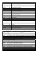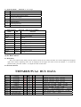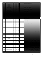
1
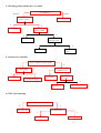
TMPA 8823-5VA4 SERVICE MANUAL
CONTENT
(1) General-----------------------------------------------------------------------------1
(2) Frame Chart-------------------------------------------------------------------fig.1
(3) IC Function Introduction ------------------------------------------------------1
3.1 N501 TMPA8823-----------------------------------------------------2
3.2 N002 ST4053 ----------------------------------------------------------3
3.3 N301 LA78040 ------------------------------------------------------------4
3.4 N601 AN7522----------------------------------------------------------4
(4) I2C Bus Control ------------------------------------------------------------------5
4.1 Menu Entry -------------------------------------------------5
4.2 Item Introduction -----------------------------------------------------------5
(5) IC Voltage --------------------------------------------------------------8
(6) Trouble shorting------------------------------------------------------------------9
1
(1) General
This chassis is consists of main IC TMPA8823-5VA4, ST4053. TMPA8823-5VA4 is an integrated circuit for a
PAL TV. A MCU and a TV signal processor (SP) are integraed in a 64-pin shrink DIP package. The MCU contains 8-bit
CPU,ROM,RAM,I/O ports,timer/counters, A/D converters,an on-screen display controller,remoter control interfaces,IIC
bus interfaces. The TV signal processor contains PIF,SIF,Video,multi-standard chroma,Sync,RGB processors.
(2) Frame Chart (see fig.1)
AV/TV SWITCH
ST4053
→
TUNER
TDL-3N1
PIF/SIF
AUDIO POWER
AN7522
VM
R, G, B
TMPA 8823
VT/BL BH/RF AGC
CRT
OSCILLLLATION
2SC3619 X 3
V-OUT
LA78040
H-OUT
ST1803DF
+115V +25V +19V
∽220V
SCAN
TRANSFORMER
BSC24-3360-4P
ON/OFF POWER
C5299 +13
fig.1
1
(3) IC Function Introduction
3.1 N501 TMPA8823-5VA4
Icon
PIN
Function: MCU and SP
Description
SDA2
1
IIC bus serial data input/output
MUTE
2
Mute Output
KEY
3
Key input
DVSS
4
GND connection
RESET
5
Reset signal input
XOUT
6
8 MHz oscillator connection
XIN
7
8 MHz oscillator connection
TEST
8
GND connection
DVDD
9
5V power supply
VVSS
10
GND connection
TV GND
11
GND terminal for Analog block
FBP IN
12
Input terminal for FBP
H.OUT
13
Horizontal driving pulse output
H.AFC1
14
H AFC filter connection
V.SAW
15
Terminal to be connected capacitor to generate V saw signal
V.OUT
16
Vertical driving pulse output
H.Vcc(9V)
17
Vcc terminal for DEF circuit
NC
18
No use
Cb in
19
Input terminal for Cb signal
Y in
20
Input terminal for Y signal
Cr in
21
Input terminal for Cr signal
DIG GND
22
GND terminal for Digital block
C in
23
Input terminal for Chroma signal
V2 in
24
Input terminal for Video signal
DIG Vdd
25
Vcc terminal for Digital block
CW out
26
Output terminal for fsc wave signal
ABCL in
27
Input terminal for ABL/ACL control
EW out
28
Output terminal for east-west correction singal
IF Vvv(9V)
29
Vcc terminal for IF circuit
TV out
30
Detected PIF signal output terminal
SIF out
31
Detected SIF signal output terminal
DC NF
34
Terminal to be connected capacitor for DC Negative feedback
PIF PLL
35
Loop filter for PIF PLL connection
IF Vvv(5V)
36
Vcc terminal for IF circuit
REG FIL
37
Terminal to be connected capacitor for stabilizing internal bias
DE-EMP
38
Terminal to be connected capacitor for SIF Det De-Emphasis
IF AGC
39
IF AGC filter connection
IF GND
40
GND terminal for IF circuit
2
IF IN
41
Input terminals for IF signals
IF IN
42
Input terminals for IF signals
RF AGC
43
RF AGC control level output
YC Vcc
44
Vcc terminal for Y/C circuit
Vsm out
45
Output terminal for Vsm signal
Black DET
46
Terminal to be connected with Black Det filter for black stretch
APC Filter
47
Terminal to be connected with APC filter for Chroma demodulation
IK IN
48
Sense ACB cathode current input
RGB Vcc
49
Vcc terminal for RGB circuit
R OUT
50
Output terminal for R signal
G OUT
51
Output terminal for G signal
B OUT
52
Output terminal for B signal
TV GND
53
GND terminal for Analog block
A GND
54
GND connection
A VDD
55
5V power supply
NC
56
SDA1
57
IIC bus serial data input/output
SCL1
58
IIC bus serial clock input
NC
59
VT
60
VT output
SCL2
61
IIC bus serial clock input
SYNC
62
Horizontal sync signal input
REMOTE
63
Remote controller signal input
POWER
64
Power control (On=Hi. Off=L)
3.2 N001\N002 ST4053
Name
Function: I2C bus control , Audio/Video switching IC
Pin
Function
RinV2
1
This pin is for input a right audio signal from an external source(V2 channel)
RinV1
2
This pin is for input a right audio signal from an external source(V1 channel)
VinV2
3
This pin is for input a composite video signal from an external source(V2 channel)
Vout
4
This pin is for output main channel composite video signal.
VinV1
5
This pin is for input a composite video signal from an external source(V1 channel)
BAND1
6
This pin is for output band1 to control tuner.
GND
7
This is the GND pin.
GND
8
This is the GND pin.
BAND2
9
This pin is for output band2 to control tuner.
BAND2
10
This pin is for output band2 to control tuner.
BAND2
11
This pin is for output band2 to control tuner.
LinV1
12
This pin is for input a left audio signal from an external source(V1 channel)
LinV2
13
This pin is for input a left audio signal from an external source(V2 channel)
Lout TV
14
This pin is for output left audio signal.
Rout TV
15
This pin is for output right audio signal.
Vcc
16
This is the power supply pin. Apply 9V to this pin.
3
3.3 N301 LA78040
PIN
Function: V-scan output
FUNCTION
1
Vertical feedback
2
Vertical working power supply
3
Pump power supply
4
Ground
5
Vertical output
6
Vertical protection
7
Vertical drive signal input
3.4 N601 AN7522
Name
Vcc
L Out
Function: Audio power amplifier
Pin
1
2,4
Function
Sound working voltage (+12V)
Sound siqnal output
Gnd
3
Ground
Mute
5
Standby
L In
6
Audio signal L input
Gnd
7
Ground
R In
8
Audio signal R input
Volume
9
Sound volume DC level 1 control
R Out
Gnd
10,12
11
Sound siqnal output
Ground
(4) I2C Bus Control
4.1 Menu Entry
Press “D” button on the factory remote control to enter the “D” mode, the letter “D” will be displayed at the upper
right coner and the adjusting items will be displayed at the upper left conrer. Press the channel +/- to select the
preferred item; press the volume +/- to adjust the value of each item.
4.2 Item introduction
TMPA8823/5VA4 BUS DATA
Comment
int
Max
1
RCUT
R CUTOFF
2C
FF
20
GCUT
G CUTOFF
20
FF
20
G Cut off
00:-0.65V,
80:0V,
FF:0.65V
BCUT
B CUTOFF
47
FF
20
B Cut off
00:-0.65V,
80:0V,
FF:0.65V
GDRV
G DRIVE
3B
7F
40
G Drive Gain
00:-4.5dB,
40:0dB,
7F:3.5dB
BDRV
B DRIVE
37
7F
40
B Drive Gain
00:-4.5dB,
40:0dB,
7F:3.5dB
CNTX
SUB CONTRAST
7F
7F
7F
Unicolor
BRTC
SUB BRIGHT CEN
COLC
2
R Cut off
51
7F
50
Brightness
2C
7F
40
Color
Tint:
TNTC
SUB TINT CEN
40
7F
40
COLP
PAL SUB COLOR
00
7F
00
00:-0.65V,
00:-20dB,
80:0V,
40:-5dB,
FF:0.65V
7F:0dB
00:1.5V(pedestal level),
00:color mute,
00:-35°,
01:-22dB or less,
40:0°,
7F:35°
4
40:2.5V,
7f:5.7dB
COLS
SECAM SUB COLOR
32
7F
40
SCOL
SUB COLOR(for
07
07
07
UV converter,
SCNT
SUB CONTRAST
09
0F
0A
Sub-Contrast
For Y Cr Cb input
0: -4.3dB,
CNTC
SUB CONTRAST CEN
3F
7F
48
CNTN
SUB CONTRAST MIN
08
7F
08
BRTX
BRIGHT MAX
20
7F
20
Difference form center
BRTN
BRIGHT MIN
20
7F
30
Difference form center
COLX
COLOR MAX
35
7F
3F
Difference form center
COLN
COLOR MIN
00
7F
00
TNTX
TINT MAX
TNTN
ST3
NTSC SHARP CEN
8:0dB,
F:3.8dB
28
7F
3F
Difference form center
28
7F
3F
Difference form center
20
3F
28
Sharpness
00:-9dB,
20:0dB,
3F:10dB
SV3
NTSC SHARP CEN
20
3F
28
Sharpness
00:-9dB,
20:0dB,
3F:10dB
ST4
OTHER SHARP CEN
20
3F
28
Sharpness
00:-9dB,
20:0dB,
3F:10dB
SV4
OTHER SHARP CEN
20
3F
28
Sharpness
00:-9dB,
20:0dB,
3F:10dB
SVD
SHARP CENTER in
19
3F
28
Sharpness
00:-9dB,
20:0dB,
3F:10dB
ASSH
Asymmetry-sharpness
09
07
04
Asymmetric sharpness
0:0dB,
4:4.5dB,
SHPX
SHARP MAX
1A
3F
3F
Difference form center
SHPN
SHARP MIN
1A
12
Difference form center
TXCX
UV COLOR MAX.
1F
1F
1F
UV SUB COLOR
For YcrCb input
RGCN
UV COLOR MIN.
16
1F
1F
UV SUB COLOR
For YcrCb input
7:8.5dB
Bit7: Nouse
Bit6: Nouse
ABL
ABL data
27
FF
35
Bit5: RGB OSD ABL
Bit4: YPL
0:ABL active for OSD
0:Y peak limiter on,105IRE,
Bit3,2:ABL Start Point
Bit1,0:ABL Gain
00:0V
01:-0.15V
10:-
00:-0.17V
01:-0.35V
10:-
0:H,V blanking on,
Bit7:Blank SW
1: Y peak
1:H,V blanking
Bit6:No use
DCBS
A part of video data
22
FF
24
Bit5,4:OSD Level
00:50IRE,
Bit3,2:Yγpoint,-3dB
00:off,
01:60IRE,
10:70IRE,
01:90IRE,
10:82IRE,
Bit1,0:No use
The data when TV mode
Bit7: F-ID
0:Normal,
Bit6: P/N ID Sens
CLTM
The data when TV
mode
04
FF
28
0:NTSC killer sensitivity,1.5mVp-
Bit5:color gamma off
Bit4,3:NTSC
1:Always killer off,i.e.
0:off,
1:on
00:NTSC1(93 ° ),
matrix
10/11:DVD for U/V inputs
Bit2,0:Y D.L.
000:-40ns
001:0ns
100:+120ns
101:+160ns
010:+40ns
110:+200ns
The data when AV mode
Bit7: F-ID
CLVO
The data when AV
mode
FF
2F
43
0:Normal,
Bit6: P/N ID Sens
Bit5:color gamma off
Bit4,3:
NTSC
1:Always killer off,i.e.
0:NTSC killer sensitivity,1.5mVp0:off,
1:on
00:NTSC1(93 ° ),
matrix
10/11:DVD for U/V inputs
Bit2,0:Y D.L.
CLVD
DEF
The data when DVD
40
FF
40
01
01
01
000:-40ns
001:0ns
100:+120ns
101:+160ns
V AGC reference, depends on
5
010:+40ns
110:+200ns
0:YC Vcc,
03
3F
00
RSNS
R SENSE
28
3F
00
GSNS
G SENSE
30
3F
00
BSNS
B SENSE
2D
3F
00
HPOS
60Hz Horizontal
17
1F
10
VP50
00
07
04
HIT
1E
3F
26
HPS
50Hz Horizontal
00
VP60
60Hz Vertical phase
02
AKB system mode(No use)
00:-3us,
10:0,
00:-47%,
1F:3us
20:0%,
3F:49%
00
7
02
0: 0H,
7:7H
HITS
50Hz Vertical size
00
VLIN
60Hz Vertical linearity
0A
F
0C
00
0:-13%,
8:0%,
F:16%
VSC
Vertical S correction
06
F
08
0:-18%,
8:0%,
F:11%
VLIS
50Hz Vertical linearity
00
00
VSS
Shift data of
00
00
BRTS
SUB BRIGHT
00
3F
00
RAGC
RF AGC
3C
3F
28
HAFC
HAFC GAIN
09
0F
09
AGCC
AGCC(Nouse))
1C
F2
1C
00:IF mute,
01:67dBu,
3F:107dBu
Bit7,6,5,4:Nouse
Bit3,2:AFC gain for AV
Bit1,0: AFC gain for TV
Bit7:VCO readjust when position select
0:enable,
Bit6,5,4,3:Nouse
FLG0
52
FF
52
Bit2:Buzz reducer
Bit1:AFT
0:on,
Window
1:off
SW
Bit0:Over Mod SW:
0:wide(-/+250kHz),
0:Normal,
1:PIF over
Bit7,6,5:Nouse
Bit4:SIF F0 Shift
FLG1
04
1F
05
Bit3:Nouse
Bit2:Mix gain:
0:SIF 1MHz convert gain, Low gain,
Bit1:Nouse
Bit0:CW SW
REFP
AKB REF pulse
0:off,
1:on,CW output form “TV
04
07
00
Nouse
00
0F
00
Bit3,2:VCD Standby
11: VCD Standby,
Bit1,0:IF Standby 11: IF Standby, other:
Bit7,6,5,4:Nouse
STBY
Bit 7-4:Nouse
SVM
VSM data
10
1F
06
Bit3,2: VSM delay
00:off,
Bit1,0: VSM Gain
00:-6dB,
01:-100ns,
10:-60ns,
01:0dB,
10:6dB,
Bit7,6,5,4:Nouse
BLK
VCEN
V centering
00
0F
00
00
3F
10
Bit3,2: V BLK start
Bit1,0: V BLK stop
00:-32%,
20:0%,
00:263H,
00:22H,
01:254H,
01:30H,
3F:30%
Bit7,6,5,4,3: Nouse
MOD
MODE
03
0F
03
Bit2:CO MAX
0:Cutoff range:-0.65 to +0.65
1:-0.65
Bit1,0: AKB cutoff sensitivity
Bit7,6,5: Chroma APC setting,
UCOM
Chroma APC Setting
00
FF
60
Bit1,0: Internal ADC,
00:GND,
10:B output,
MODE3
80
FF
011:normal
Bit4,3,2: Nouse
80
6
01:R output,
11:Monitor RF
setting
Bit7,6: No use
Bit5: Video mute type
0:R\G\B mute,
1:Y mute
Bit4,3,2,1,0: Mute time (×8ms)
Bit7,6,5,4,3: No use
NOIS
HAFC control
01
07
01
Bit2: AFC fix
Bit1,0: Noise threshold
SYCT
PYNX
08
FF
08
H.SYNC MAX in
28
PYNN
H.SYNC MIN in
18
3F
18
PYXS
H.SYNC MAX in
22
3F
22
PYNS
H.SYNC MIN in search
1E
Nouse
28
3F
1E
ONTM
00
FF
00
Video mute time setting when Power On(×16ms)
NSHP
1A
3F
10
Sharpness data offset when Noise Reduction is On.
V01A
VOLUME 1%
04
3F
09
Volume output data when volume=1
V25A
VOLUME 25%
3D
7F
24
Volume output data when volume=25
V50A
VOLUME 50%
57
7F
40
Volume output data when volume=50
V100A
VOLUME 100%
72
7F
72
Volume output data when volume=100
Bit7: Nouse
Bit6: bass boost SW
WCTL
APRO mode data
01
7F
41
0:off,
Bit5: input attenuator
Bit4: ALS SW
1:on
0:0dB,
0:off,
Bit3,2: ALS start point
Bit1,0: woofer fc
1:-5dB
1:on
00:220mv,
00:100Hz,
01:125Hz,
01:380mv,
10:170Hz,
Bit7,6,5: No use
SUR1
Surround data (mono)
07
1F
06
Bit4,3: Input matrix 00:normal,
01:R ch,
Bit2,1,0: Surround level: 000:off,
10:L ch,
001-111:surround
Bit7,6,5,4: Nouse
SUR2
Surround data (stereo1)
07
0F
0C
Bit3: Surround mode1:
0:φ
1:4φ
Bit2,1,0: Surround level: 000:off,
001-111:surround
Bit7,6,5,4: Nouse
SUR3
Surround data (stereo2)
0F
0F
0F
BASC
BASS Center
40
72
40
Bit3: Surround mode1:
0:φ
1:4φ
Bit2,1,0: Surround level: 000:off,
001-111:surround
User Bass Level
BASX
BASS MAX
72
72
72
User Bass Level
TREC
TREBLE Center
40
72
40
User Treble Level
BALC
BALANCE Center
3F
72
40
User Balance Level
WOFC
WOOFER Center
39
7F
40
User Woffer Level
BAS1
BASS data in “Music”
68
CB
Bit0-6: Bass level,
bit7:Surround select.0
BAS2
BASS data in “News”
40
FF
3C
Bit0-6: Bass level,
bit7:Surround select.0
BAS3
BASS data in “Theater”
4A
FF
CB
Bit0-6: Bass level,
bit7:Surround select.0
TRE1
TREBLE data in
68
FF
55
Bit0-6: Treble level,
bit7:Surround select.1
TRE2
TREBLE data in
40
FF
37
Bit0-6: Treble level,
bit7:Surround select.1
bit7:Surround select.1
TRE3
TREBLE data in
54
FF
A8
Bit0-6: Treble level,
WFL1
Woofer data in “Music”
F2
FF
CB
Bit0-6: Woofer level,
bit7:Woofer On/Off
1:On
WFL2
Woofer data in “News”
31
FF
99
Bit0-6: Woofer level,
bit7:Woofer On/Off
1:On
WFL3
Woofer data in
D9
FF
E4
Bit0-6: Woofer level,
bit7:Woofer On/Off
1:On
WON1
Woofer output level
0A
FF
05
For the calculation of the Woofer output value.
WON2
Woofer output level
09
FF
09
For the calculation of the Woofer output value.
WOFF
Woofer output level
00
FF
00
A Woofer output level in Woofer off.
AUCON1
Stereo/SAP noise
88
FF
88
Bit0-3: ST0-ST3
7
threshold
Bit4-7: SP0-SP3
Bit0-3: L0-L3
AUCON2
Level adjust setting
08
FF
03
Bit4-6: Nouse
Bit7: STS
AUALI1
For wideband expander
10
FF
00
AUALI2
For spectral expander
10
FF
00
03
FF
03
AUTIM
Timing current
AUSTP
alignment data
Audio step
01
0F
01
VPCT
X-ray protection
02
FF
02
Bit0-4: A10-A14
Bit5-7: Nouse
Bit0-4: A20-A24
Bit5-7: Nouse
Bit0-2: TC0-TC2
Bit3-7: Nouse
Nouse
TUNR
01
02
00
0:Toshbia, 1:ACOM,
CCDOSD
2E
7F
22
OSD horizontal position for CCD
2:ALPS
CCDOSDF
59
FF
59
OSD frequency for CCD
OSDF
51
69
53
OSD frequency
OSD
10
7F
22
OSD horizontal position
PANDA OPTION0
Bit7: Nouse
Bit6: Fjp snd menu 0:off, 1:on 关闭立体声菜单
PDOPT0
PANDA
OPTION0
FF
Bit4: Fjp vchip 0:off,
Curce
curste
1:on
Bit3: Flang portguese: 0:off,
Bit2: Flang Spanish
Waiting time
1:on 南美三制式
Bit5: Fmulti colorsys 0:off,
03
2F
FF
58
Curtain center
A5
FF
A5
Curtain open/close step
02
08
02
PWR
Self check data
00
FF
00
BUS
Self check data
00
03
00
MEM
Self check data
00
FF
00
0:off,
1:on
1:on
Bit1: Fjp close screen
0:off, 1:on
Bit0: Fjp open screen
0:off, 1:on
Waiting time before curtain open
Bit7: Fsync det blue back (set 1)
Bit6: Nouse
Bit5: Fsync det ( set 0)
OPT
Optional setting
1F
FF
Bit4: When B.B,OSD frequence
0:50Hz,
1:60Hz
Bit3: Ftb1231n audio gain(au gain VCD 14h)
Bit2: Fymute use
Bit1: F bb exmute
Bit0: F bb mute
Bit7: Fjp stereo (select 1343) 1:select 0:unselect 立体
Bit6: set 0
Bit5 :Fdvd audio av2
OPTM1
Optional setting1
22
FF
Bit4: no use
Bit3: set 0
Bit2: Fjp pwm balance
Bit1: Fjp pwm8 volume
Bit0: Fsel video2
OPTM2
Optional setting
02
FF
Bit7: Fjp sanyokey
Bit6: Fjp swoofer
8
Bit5 :set 0
Bit4: Fselect tda9850 打开
Bit3: Fslice level,
Bit2: F lan s out (shop out spanlish)
Bit1: F lan p out (shop out portguese)
Bit0: Fmono avout 0:mono 1: stereo
OPTM3
Option setting
01
FF
Note: the bold date cannot be changed
(5) IC voltage
N501 TMPA8823
PIN
1
2
3
4
5
6
7
8
9
10
11
12
13
Voltage
/
/
/
0
5
2.4
2.3
0
5
0
0
1.1
1.9
PIN
14
15
16
17
18
19
20
21
22
23
24
25
26
Voltage
6.6
4.2
4.7
9
/
2.5
2.5
2.5
0
2.5
2.5
3.3
/
PIN
27
28
29
30
31
32
33
34
35
36
37
38
39
Voltage
4.9
4.6
9
5.1
1.8
4.1
3
2.3
2.4
5
2.2
4.4
4.2
PIN
40
41
42
43
44
45
46
47
48
49
50
51
52
Voltage
0
0
0
4.5
2.7
2.7
1.9
2.6
0
9
2.5
2.5
2.5
PIN
53
54
55
56
57
58
59
60
61
62
63
64
Voltage
0
0
5
/
4.8
4.8
/
/
/
4.4
2.5
/
N001\N002 ST4053
PIN
1
2
3
4
5
6
7
8
9
10
11
12
13
Voltage
4.4
4.4
0
0
0
0
0
0
0
0
0
3.3
3.3
PIN
14
15
16
Voltage
3.1
4.4
9
N301 LA78040
PIN
1
2
3
4
5
6
7
Voltage
2.9
23.6
2.1
0
10.7
23.8
2.9
N601 AN7522
PIN
1
2
3
4
5
6
7
8
9
10
11
12
Voltage
12
5.4
0
5.4
3.7
1.46
0
1.46
3.5
5.4
0
5.4
9
(6). Trouble shorting
T804
9
Rectifying
and
Detection
B1
+115V
H.OUT
Power supply
12
Rectifying
and
Detection
B2
+27V
V.OUT
Power supply
16
Rectifying
and
Detection
B3
+12V
Audio
Power
supply
Power supply outline
6.1 No grating, no picture, no sound
General, these failures are produced by power sources, because of which refer to a wider area, so that can be divided them
two conditions to explain: no B1 115 V and existing B1 115V.
(1) No B1 (115 V) voltage (voltage of network 220 V ac)
These failures may be caused by power supply switch.
Check voltage+B
0V
Check C807(+) voltage
0V
300V
Check V813 b
voltage
Check C807,V813
at
condition of
short-circuit?
Replace the
parts of
failure
0.5V
0V
Y
Check V813 b voltage
Check R820 R811
V813
0.7V
Check T804
(2) Existing B1 115 V
0
Check VD814 VD817
VD818 C814 C815
C817
These failures may be caused by abnormal operation of horizontal scan, to confirm which can observe the filament of
10
tube whether bright on. If determined horizontal scan in abnormal operation, look for the failure start from the horizontal
drive stage. Search upward to TMPA8821 with method of checking DC voltage and waveform according to sequence:
PIN13/H.OUT port→ PIN17 power supply→ N802/9V output.
Check voltage at 17 pin of
TMPA8821 =9 V
N
Y
Check voltage at 13
pin of TMPA8821
=1.9 V
Check B2(27V)
voltage
0
Check VD853
N
Y
27V
Check N501
Check V431 T402
Check V898 R850
6.2 Existing grating and no picture
Check OSD on screen
Y
N
Check N501 N701 G701
Check the voltage of PIN29
36 44 49 of N501
Normal
Abnormal
Check V2in waveform
Check N001
existed at PIN24 of N501
* : Whenever open or
N
Y
interconnect on the bus from
CPU to E2PROM and main
chip, no picture can occur.
Check TVin waveform
at N001/PIN14
Check N501
Y
Check N001
N
Check circuit between
PIN41~PIN42 of N501
11
6.3 Existing grating and picture, no sound
Check the audio signal of + pins of
two loudspeaker
Normal
Abnormal
Check waveform at
pin2 4 of N501
Check loudspeaker
Y
N
Check N501
Check waveform at
pin15 of N002
N
Y
Check waveform
at pin 4of N002
Check N501
Y
N
Check
C010
Check R023
N002
6.4 Cannot save channels
When searching automatically channels,
observe whether can display picture
N
Y
Check SYNC waveform
at N501/PIN62
Y
Check VT voltage of
TUNER=0--30 V
N
Y
N
Check 33 V of
voltage
Check tuner
Check N501
Check SYNC waveform at
V708 V709 V710
N
Y
Check N501 V713
Check R723 and N721
6.5 CPU non-operating
Check voltage at PIN9 54 of N501 =5V
N
Y
Check voltage at
N501/PIN5(RESET)=5V
Check N803 T804
Y
Check N501 G701
N
Check V703 VD701
12
13
N° Boletín
Fecha
2166
21/06/2006
Identificación del Producto
TELEVISOR COLOR
Modelos
TVS-1430 MA
TVS-2142MA
TVS-2152PF
Procedencia / Marca
SANYO
Falla Reportada / Motivo :
METODO PARA ENTRAR AL MODO DE SERVICIO
DEL TELEVISOR.
Solución aplicada :
La “D” en el Manual de Servicios significa Modo “D”. Los modos de fábrica son el Modo “S” y el
Modo “D”. En el modo “S” sólo se pueden ajustar algunos parámetros; mientras que en el modo
“D” se pueden ajustar todos los parámetros. Para los Chasis TMPA8823 (TV´s de 14” hasta
21”) y TMPA8859 (TV´s de 25” hasta 34”), se puede acceder al modo “S” utilizando el control
remoto del usuario siguiendo los siguientes pasos:
Presione el botón VOL - en el panel de la TV hasta 0 (no suelte el botón VOL -), luego presione
el botón DISPLAY en el control remoto para entrar al modo S.
Si se quiere acceder al modo “D”, para el Chasis TMPA8823 (TV´s de 14” hasta 21”), siga los
siguientes pasos utilizando el control remoto:
Primero siga los pasos para entrar al modo “S”.
Presione el botón DISPLAY en el Control Remoto.
Presione el botón VOL - en el panel de la TV hasta 0 (no suelte el botón VOL -), luego presione
el botón DISPLAY en el control remoto para entrar al modo D.
Técnico emisor
Uso interno
Roberto Quiñones M.
Revisado por
V°B°
J C. Zambrano.
INCLUYA ESTA INFORMACIÓN EN SU MANUAL DE SERVICIO
J.C.Z.B.
TMPA8821 AV STEREO DVD 2 IN 1
R OUT
W OUT
R
R721
22KΩ
R763
15K
1
N706
GP1UX511QS
KEY
2
R201
150
R204
150
V704
2SC1815Y
VD763
1N4148
R701
1KΩ
R702
10KΩ
VD762
1N4148
C411
0.01
L105
TRF0459
C233
1uF
16V
38
39
I F GND
I F AGC
40
41
I F IN
42
43
I F IN
RF AGC
44
YC 5V
45
46
BLACK DET
MONI T-O UT
48
47
I K-I N
C228
1000
C231
22uF
16V
C232
0.01
37
C506
0.01
C527
10uF
16V
C129
0.47uF
16V
R523
100KΩ
R221
150
SIF
C226
10uF
16V
C227
0.47uF
16V
C529
10uF
16V C131
10uF
16V
+
SCK
SDA
STB
C870
10uF
16V
ON
1
AGC
4
2
VT
BAND1
N001
TC4053BP
AV1/AV2
2
3
3
2
C010
1uF
16V
C007
1uF
16V
3
2
1
R015
100
8
7
6
5
3
1
R023
100
L-IN 2
1
8
7
6
5
4
XS003
V-IN 2
4
9
10
11
12
13
14
15
5
1
R-IN 2
R030
100
C221
0.1
TV-R
EXT-A UDIO
R135
220
V106
2SA1015Y
TV-L
R040
22kΩ
R033
22KΩ
4
R032
22KΩ
R029
22KΩ
2
1
L111
8.2uH
R134
100
R130
220
R129
100
C133
47uF R241
47
16V
R132
330
R133
390
X102
X5.5MHz
2Vp-p
X101
X6.5MHz
XS202
V105
2SC1815Y
R619
3.3KΩ
V902
2SC2482
R902
100
R914
RGB_OUT
XS201
XP201
5
9V
2
C-IN
R
3
4
G
2
5
B
1
C904
470
L201
100uH
4
3
2
1
1
VD902
1SS133
R916
4.7K
GND
1
H.VCC
XP202
2
2W18K
R131
1KΩ
L109
10uH
1Vp-p
R857
12
0.5W
R037
22KΩ
3
C018
47uF
16V
C132
0.01
V104
2SC1815Y
C130
0.01
R136
3.3KΩ
5
R
R041
2.2KΩ
R858
470
OFF
16
9
10
11
12
13
1
C551
100uF
16V
R031
1KΩ
32
31
30
SIF- OUT
TV- OUT
I F- VCC(9V)
AUDI O-O UT
VD509
1SS133
29
28
27
26
TV- IN
DI GI 3.3V
25
EXT-I N
24
C-I N
TV GN D
23
22
Cr
Cb
Y- IN
20
19
21
C523
0.47uF
16V
C530
0.1
R528
270
0.5W
V855
2SC2655
R582
10KΩ
NEXT
L508
27uH
R238
1KΩ
VD420
MTZJ-6.2B
VD701
HZ3.6V
NC
H- VCC
18
17
C410
1000uF
16V
C527
0.01
R525
100
L402
47uH
R737
470
R710
4.7KΩ
R522
100
C521
0.1
C522
22
R301
15KΩ
N002
TC4053BP
AV/TV
V005
2SC1815Y
S-REG
C509
1uF
16V
R509
220KΩ
APC FIL
50
49
V- OUT
V- SAW
16
15
C309
0.47uF
16V
C408
0.47uF
16V
R446
10KΩ
AV-2 Board
C006
1uF R013
16V 100
XP004
XS002C
L
R128
3.3KΩ
C507
100uF
16V
R510
30KΩ
R-O UT
G- OUT
14
H.A FC
H- OUT
SCP- OUT
13
12
GND
11
GND
+5V
9
10
C706
0.01
R411
8.2KΩ
R-IN 1
R035
22KΩ
XS004
C511
0.22
16V
C510
2200
R516
270
RGB 9V
52
51
53
GND
GND
B-O UT
55
54
56
TV/AV 1/AV2
R517
270
C407
8200
L701
10uH
R736
8.2KΩ
14
16
C704
22
V856
2SC1815Y
1.8K
10uF/16V
C705
10uF
16V
R709
1KΩ
V703
2SA1015Y
R881
10KΩ
V761
2SA1015
VD707A
FR205
R769
C783
C701
0.01
R708
33KΩ
R770
470
R771
470
STOP
VD764
1N4148
R761
10KΩ
TEST
X- TAL
8
7
G701
8M
C702
0.01
C703
22
OPEN
S710
5V
58
SCL1
57
60
X- TAL
RESET
R207
1KΩ
6
GND
5
1
R751
47
KEY
BAND1
R765
110K
S707
S709
R518
270
3
C552
0.01uF
C229
470uF
16V
C615
0.01uF
MENU
PLAY
C744
0.01
R743
100
R745
1KΩ
59
63
RMT- IN
C741
100
R231
1KΩ
C513
100uF
16V
C514
0.01
R703
1KΩ
+
TV/AV
S706
R704
10KΩ
4
C781
47uF/16V
3
R764
30K
S705
C747
27
C230
0.01uF
AV_1
C009
1uF
16V
R011
100
AV2
R036
22KΩ
TV
+5V-2
L204
12uH
R265
3.3KΩ
3
BAND2
V-
2
V+
S704
POWER
R715
47
R762
11K
S703
C516
10
TMPA 8821
P-
C746
330
V705
2SC1815Y
N501
S702
C517
10
C745
10uF
16V
R744
10KΩ
VT
RI
R232
1KΩ
R705
10KΩ
VOL
GND
5
100PF
62
KEY
4
R733
10KΩ
61
3
R235
1KΩ
64
C751
XS1702
MUTE
5V
+
47uF/16V
S701
XP701
2
H.SYNC
9V
1
R761
5.6K
C518
10
C015
0.01
C013
0.01
N504
AN7805
L707
10uH
R746
10KΩ
L-IN 1
AV1
A
C016
47uF
16V
V-IN 1
C005
1uF
16V
R025
100
AV
Sync.
R728
10KΩ
SDA1
470
P+
R729
10KΩ
L503
10uH
R734
22KΩ
R101
120
R104
910
R108
33
RMT-IN
R753
0
2SC388ATM
R756
12KΩ
3
8
R730
47
R752
360
C782
R254
open
C014
47uF
16V
C004
1uF
16V
R008
100
AV1/AV2
R022
1KΩ
R034
10
2
VCC
C749 C750
10uF
0.01 16V
R-OUT
R005
2.2KΩ
1
A0
C764
6
7
XP1301
C011
10uF
16V
R006
1KΩ
R727
2.2MΩ
IF
33
TEST
R102
100
SIF- IN
1
SCL
A1
R758 1500
3.9KΩ
5
SDA
A2
33KΩ
C723 C724
0.1 0.1
R021
1KΩ
C102
1000
V101
R259
100
R028
100
L
R726
33KΩ
R103
3.3KΩ
V708
2SA1015Y
35
2
R751
680
R752
560KΩ
R725
C722
0.1
R
C105
0.01
34
VSS
3
R760
2.2KΩ
DC NF
4
R753
68KΩ
V709
2SA1015Y
C761
1uF
16V
33KΩ
TV/AV
PIF PLL
VOL
R757
3.9KΩ
XP001
AV_OUT
L-OUT
C002
10uF
16V
R027
2.2KΩ
C721
220
R107
560
R?
36
MUTE
C765
2700
C104
0.1
Z101
D2959M
R724
220
V002
2SC1815Y
15
C763
33uF
16V
V710
2SC1815Y
BAND
R755
470
C762
180
R722
V703
2SC1815Y
L103
1uH
R100
220
AV2
R026
1KΩ
VD721
1SS133
33KΩ
N721
upc574
VT
AV1
VD707
FOG205
C125
4.7uF
V701
2SC1815Y
N701
AT24C08A
XP002C
R009
75
V004
2SC1815Y
R723
+33V
C126
0.1
C608
1uF
16V
TV
R750
R128
12KΩ
2W
+110V
TV/AV
R787
10KΩ
1
R004
100
2
R730
3.9KΩ
VD603
1SS133
2
XS802
R003
220
AV1/AV2
I F- VCC(5V)
R607
10KΩ
R002
75
C001
470uF
16V
V-OUT
V702
2SC1815Y
R606
22KΩ
C609
4.7uF
16V
S708
3
1
C000
100uF
16V
R764
10KΩ
R788
1.5KΩ
C611
2.2uF
16V
R609
47KΩ
4
2
V108
2SC1815Y
4
R747
10KΩ
R620
10KΩ
R612
10KΩ
R610
1KΩ
BAND2
R000
100
0.5W
Audio out
R
+9V
VD602
1SS133
V601
2SC2878A
6
8
R
VD601
1SS133
+9V
1
3
3
L
DVD UNIT
2
12
C625 C626 C627
2.2uF 4.7uF 0.027
16V 16V
XP1502 5
2
C624
2.2uF
16V
C643 C623
0.039 0.015
XS001
DE- EM PH
C612
1uF
16V
MB
IF
HPF ( L)
HPF ( R)
11
10
9
GND
L IN
7
8
Por t 4 (Φ2)
O.C (Φ1)
6
5
4
Por t 3 (Φ3)
C643
0.01
3
R007
75
1
C644
0.039
5
2
XS602
C109
4.7uF
16V
C003
C-IN
0.01
ABCL-I N
XP602
C621
47uF
16V
R114
56kΩ
C111
0.47UF
4
C-IN
R108
100
V602
2SA1015Y
15KΩ
C110
0.47UF
BAND
L
2
C107
220uF
16V
C108
0.01
1
L-OUT
5W/8Ω
R113
+5V-2
2
5W/8Ω
U101
TUNER-5V
L101
47uH
W271
open
13
16
14
LPF (L)
LPF ( R)
18
17
L OUT
Filter
19
15
LPF1
V.F
LPF2
21
20
LPF3
Vcc(9V)
24
23
22
W.F
SCL
W270
open
C628
8200
C602
2.2uF
16V
R603
2.2KΩ
3
N603
C645
10uF
16V
Por t 2 (Φ4)
VD682
HZ6V2
1
R-OUT
C632
0.01
TA1304N (TA1343N)
Por t 1 (O.C)
VD681
HZ6V2
2
R680
5.6KΩ
+5V-2
C601
2.2uF
16V
1
L
R602
5.6KΩ
R618
100
R
C630 C629
0.027 8200
XP702
R605
68KΩ
R
C631
0.01
L
C634 C633
0.047 0.033
R IN
C619
0.01
R608
270KΩ
R601
5.6KΩ
TA1343N
R683
18KΩ
C637
3.3uF
16V C636 C635
0.01 0.022
R615 R616
100 100
SDA
VCC
GND
OUT1
STANDBY
OUT1
1
2
3
I N1
GND
I N2
VOL
OUT2
GND
OUT2
V682
2SC2878A
R682
18KΩ
+12V
C607
47uF
16V
C606
4.7uF
16V
R604
2.2KΩ
XS601
4
5
6
7
8
9
10
11
12
XP601
V681
2SC2878A
C618
470uF
25V
C605
4.7uF
16V
SDA
VD683
HZ5V6
C604
0.01
C603
0.01
SCL
R617
100
C621
100uF
16V
C622
0.01
+9V
5
R614
10
N601
AN7522N
R913
470
VE1
R915
1.2K
R920 1.2K
VD870
10BSA
R925 1.2K
V903
2SC2482
ABL
R903
100
SCP
2
3
XP702
SDA
SCK
SCS
5
IRINT
6
VDD
C868
220uF
16V
1
4
L407
HXC-3AB
N301
LA78040
XP802
!
XS802
3
2
T803
LQ 0002
C803-C806
1000
1KV
!
3
C807
150uF
450V
R820
120KΩ
0.5W
1
1
R802
3.9
7W
!
XP801
!
!
T802
LQ0002
R811
5.6KΩ
R822
15KΩ
C501
0.1µF
250VAC
SW801
KDC-A06
R824
39
2W
C814
0.047
VD817
ES1
C851
470
C816
680
2KV
1KV
9
!
V898
B892
R896
10KΩ
! F801
3.15A/250V
V811
2SA1015Y
VD819
HZ7.5
R823
2.2KΩ
VD816
1SS133
R817
1KΩ
R826
2.7KΩ
R815
22KΩ
C815
0.015
!
14
C817
0.015
2
!
C864
1000uF
25V
8
R831
0.5W12MΩ
!
C831
2200
AC400V
C855
470
500V
Ref erence
7
Out Vcc
6
Output
5
GND
Punp Up
4
3
C302
open
R448
1W12K
R869
1
1W
V899
B892
R862
1
1W
C865
1000uF
25V
1
C820
0.01
+12V
H.VCC
R870
27
2W
R898
10KΩ
VD855
ES1
!
+13V
R899
1.2KΩ
N802
AN7809
C821
470uF
3 16V
R308
150
2W
V431
R432 2SC2383
330
R434
1KΩ
0.5W
+9V
T402
AD0002
C436
7n2
1.6KV
C305
2.2uF
R306
15KΩ
R307
10KΩ
C306
1000uF
25V
R433
330
!
5
C435
2n7
2KV
3
4
1
L405
TEM2011Y
C431
390
500V
2
10
C433
47uF
35V
R435
270
+110V
2W
R460
0.5W220K
XS402
1
+180V
VD901
1SS133
R921
4.7K
2
XP402
3
4
1 180V
R923
470
C902
470
2 HEAT
R444
220KΩ
0.5W
T401
BSC-3360-4P
R924
2W 18K
V910
2SC2482
XP402
R205
10K
V905
C2120
3 GND
4
6
L404
TEM2011Y
C432
1000
500V
R312
1
1W
C822
0.01
V432
2SD1555
!
C308
0.22
VD301
EU2A
C441
250V10u
R445
RF10-1W2.2
C440
2200
500V
H-OUT
C307
100uF
35V
C309
220uF
35V
1
1
HEAT
C443
0.39uF
400V
C303
0.22
R305
47KΩ
VD854
EU2Z
V812
2SC3807
Vcc
I nput
+24V
1
R801
! 3.3MΩ
0.5W
C301
1500
R897
3.9KΩ
C854
470
500V
2
2
R904
100
VD410 EU1C
R304
2.7KΩ
R302
1
0.5W
R850
0.22
0.5W
3
R450
1KΩ
1W
C304
10uF R303
16V 3.9KΩ
VD888
R2M130V
VD861
HZ6.2
C863
470uF
35V
C853
470
1KV
+110V
R863
47KΩ
0.5W
R856
22KΩ
R853
5.6KΩ
VD853
RU3Y×1SF22
13
V853
2SC1815Y
RP851
B-2K
12
V813
2SC4236
R819
22
VD818
1SS133
R852
100KΩ
0.5W
11
10
7
VD814
1SS133
!
T801
BCK-70-01D-2
R825
68
2W
2
VD803~VD806
TVR4N
RT801
MZ73B-18Ω
1
2
!
R854
150KΩ
0.5W
C861
220uF
160V
1
VD851
BYT56M
C902
2KV2000P
R918
470
C906
470
3
V-OUT
N801
PC817
C834
AC400V470p
LHDY
4
5
+9V
C869
0.01
StandBy
!
L410
XS401
3
+5V-1
R919
2W 18K
VD903
1SS133
R917
4.7K
N803
AN7805
4
2
1
R766 ~ R768
220K×3
GND
C909
470uF
C444
1uF
160V
HV
16V
R909
82
C907
0.47uF
KFC
C908
0.47u
VD905
1SS133
KSC
7
C423
0.056
100V
R436
3.9
6W
R1302
C400
33uF
160V
R1507
R442
10KΩ
R439
20KΩ
XS1501
VD1501
RU4YX
22K
C1302
V1500
3DD880
XP1502
1
+
VD899
1SS133
C1500
470
R1503
120
C1504
0.01
+
C1503
1000uF/16V
VD1502
6B1
B1
XS1503
1
B2
GND
2
3
OPTICAL
68
+5V-2
C1501 C1502
1000uF/16V0.01
GND
2
5V-2
3
GND
4
5V
5
NC
0.1
R1304
330
COAXIAL
R1303
91
S1301
XP1302
C1301
0.1
VD1506
6B2
V1501
2SC1815
+ C1505
10uF
1
2
1
R1501
8.2K
2
R1301
10K
XS1301