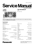
1
HT-ST9 SA-ST9 SERVICE MANUAL Ver. 1.1 2015.06 • All of the units included in the HT-ST9 (SAST9/SA-WST9/Remote control) are required to confirming operation of SA-ST9. Check in advance that you have all of the units. Photo: SA-ST9 US Model Canadian Model AEP Model UK Model Australian Model Chinese Model Singapore Model Taiwan Model Latin American Model Note: Be sure to keep your PC used for service and checking of this unit always updated with the latest version of your anti-virus software. In case a virus affected unit was found during service, contact your Service Headquarters. COMPONENT MODEL NAME HT-ST9 Bar Speaker (Active Speaker System) SA-ST9 Subwoofer (Active Subwoofer) SA-WST9 • Please refer to service manual separately issued for Subwoofer. SPECIFICATIONS Amplifier section BLUETOOTH section U.S. models: POWER OUTPUT AND TOTAL HARMONIC DISTORTION: (FTC) Front L + Front R: With 6 ohms loads, both channels driven, from 200 - 20,000 Hz; rated 25 Watts per channel minimum RMS power, with no more than 1% total harmonic distortion from 250 milliwatts to rated output. POWER OUTPUT (reference) Front L/Front R speaker blocks: 75 Watts (per channel at 6 ohms, 1 kHz) Center speaker block: 75 Watts (per channel at 6 ohms, 1 kHz) Center tweeter block: 75 Watts (per channel at 6 ohms, 10 kHz) Communication system BLUETOOTH Specification version 3.0 Output BLUETOOTH Specification Power Class 1 Maximum communication range Line of sight approx. 30 m (98.4 ft) 1) Maximum number of devices to be registered 9 devices Frequency band 2.4 GHz band (2.4GHz - 2.4835 GHz) Modulation method FHSS (Freq Hopping Spread Spectrum) Compatible BLUETOOTH profiles 2) A2DP 1.2 (Advanced Audio Distribution Profile) AVRCP 1.5 (Audio Video Remote Control Profile) Supported Codecs 3) SBC 4) , AAC 5) , LDAC Transmission range (A2DP) 20 Hz - 20,000 Hz (Sampling frequency 44.1 kHz) Canadian models: POWER OUTPUT (rated) Front L + Front R: 45 W + 45 W (at 6 ohms, 1 kHz, 1% THD) POWER OUTPUT (reference) Front L/Front R speaker blocks: 75 Watts (per channel at 6 ohms, 1 kHz) Center speaker block: 75 Watts (per channel at 6 ohms, 1 kHz) Center tweeter block: 75 Watts (per channel at 6 ohms, 10 kHz) 1) Chinese model: POWER OUTPUT Front L/Front R speaker blocks: 30 Watts (per channel at 6 ohms, 1 kHz) Center speaker block: 30 Watts (per channel at 6 ohms, 1 kHz) Center tweeter block: 30 Watts (per channel at 6 ohms, 10 kHz) Other models: POWER OUTPUT (rated) Front L + Front R: 50 W + 50 W (at 6 ohms, 1 kHz, 1% THD) POWER OUTPUT (reference) Front L/Front R speaker blocks: 75 Watts (per channel at 6 ohms, 1 kHz) Center speaker block: 75 Watts (per channel at 6 ohms, 1 kHz) Center tweeter block: 75 Watts (per channel at 6 ohms, 10 kHz) Inputs HDMI IN 1*/2/3 DIGITAL IN (TV) ANALOG IN Output HDMI OUT* (ARC) * HDMI IN 1 and HDMI OUT (ARC) jacks support HDCP 2.2 protocol. HDCP 2.2 is newly enhanced copyright protection technology that is used to protect content such as 4K movies. HDMI section Connector Type A (19pin) USB section (USB) port: Type A (For connecting USB memory, memory card reader, digital still camera) LAN section LAN (100) terminal 100BASE-TX Terminal Wireless LAN section Standards Compliance IEEE 802.11 a/b/g/n Frequency band (Except Chinese model) 2.4 GHz, 5 GHz Frequency band (Chinese model) 2.4 GHz - 2.4835 GHz 5.15 GHz - 5.35 GHz 5.725 GHz - 5.85 GHz 9-896-148-02 2015F33-1 © 2015.06 2) 3) 4) 5) The actual range will vary depending on factors such as obstacles between devices, magnetic fields around a microwave oven, static electricity, cordless phone use, reception sensitivity, the operating system, software applications, etc. BLUETOOTH standard profiles indicate the purpose of BLUETOOTH communication between devices. Codec: Audio signal compression and conversion format Subband Codec Advanced Audio Coding Front L/Front R speaker blocks Speaker system 2-way coaxial speaker system, Acoustic suspension Speaker Woofer: 65 mm (2 5/8 in) cone type, Magnetic fluid speaker Tweeter: 18 mm (23/32 in) soft dome type Center speaker block Speaker system Center 2-way coaxial speaker system, Acoustic suspension Satellite Full range speaker system, Acoustic suspension Speaker (5 speakers) Center Woofer: 65 mm (2 5/8 in) cone type, Magnetic fluid speaker Tweeter: 18 mm (23/32 in) soft dome type Satellite 65 mm (2 5/8 in) cone type, Magnetic fluid speaker General Power requirements 120 V AC, 60 Hz (US and Canadian models) 120 V AC, 50 Hz/60 Hz (Taiwan model) 120 V - 240 V AC, 50 Hz/60 Hz (Latin American model) 220 V - 240 V AC, 50 Hz/60 Hz (Other models) Power consumption On: 60 W Standby mode: 0.5 W or less BLUETOOTH Standby mode: 0.5 W or less (Except AEP and UK models) Networked Standby (all wired network ports connected, all wireless network ports activated): 7.3 W (AEP and UK models) Sony Corporation Published by Sony Techno Create Corporation Dimensions (approx.) (w/h/d) 1,130 mm × 88 mm × 128 mm (44 1/2 in × 3 1/2 in × 5 1/8 in) (without grille frame, without stands, including projection portion) 1,130 mm × 88 mm × 133 mm (44 1/2 in × 3 1/2 in × 5 1/4 in) (with grille frame, without stands) 1,130 mm × 100 mm × 129 mm (44 1/2 in × 4 in × 5 1/8 in) (without grille frame, with stands, including projection portion) 1,130 mm × 101 mm × 136 mm (44 1/2 in × 4 in × 5 3/8 in) (with grille frame, with stands) Mass (approx.) 6.8 kg (14 lb 15 7/8 oz) (without grille frame, without stands) Compatible iPod/iPhone models The compatible iPod/iPhone models are as follows. Update your iPod/ iPhone with the latest software before using with the system. BLUETOOTH technology works with: iPhone 6 Plus/iPhone 6/iPhone 5s/iPhone 5c/iPhone 5/iPhone 4s/ iPhone 4/iPhone 3GS iPod touch (5th generation)/iPod touch (4th generation) Wireless transmitter section Communication system Wireless Sound Specification version 3.0 Frequency band (Russian model) 5.2 GHz (5.180 GHz - 5.240 GHz) Frequency band (Chinese model) 5.15 GHz - 5.25 GHz Frequency band (Latin American, Singapore and Taiwan models) 5.8 GHz (5.736 GHz - 5.814 GHz) Frequency band (Other models) 5.2 GHz (5.180 GHz - 5.240 GHz) 5.8 GHz (5.736 GHz - 5.814 GHz) Modulation method DSSS – Continued on next page – HT-ST9 SOUND BAR SA-ST9 ACTIVE SPEAKER SYSTEM HT-ST9 Ver. 1.1 Apple, the Apple logo, iPhone, iPod, iPod touch, and Retina are trademarks of Apple Inc., registered in the U.S. and other countries. App Store is a service mark of Apple Inc. Video formats supported by the system Input/Output (HDMI Repeater block) 3D Format 2D Frame packing Side-bySide (Half) Over-Under (Top-andBottom) 4096 × 2160p @ 59.94/60Hz 1) 4096 × 2160p @ 50 Hz 1) 4096 × 2160p @ 23.98/24 H z 2) 3840 × 2160p @ 59.94/60Hz 1) 3840 × 2160p @ 50 Hz 1) 3840 × 2160p @ 29.97/30 Hz 2) 3840 × 2160p @ 25 Hz 2) 3840 × 2160p @ 23.98/24 Hz 2) 1920 × 1080p @ 59.94/60 Hz 1920 × 1080p @ 50 Hz 1920 × 1080p @ 29.97/30 Hz 1920 × 1080p @ 25 Hz “Made for iPod,” and “Made for iPhone” mean that an electronic accessory has been designed to connect specifically to iPod or iPhone, respectively, and has been certified by the developer to meet Apple performance standards. Apple is not responsible for the operation of this device or its compliance with safety and regulatory standards. Please note that the use of this accessory with iPod or iPhone may affect wireless performance. “BRAVIA” logo is a trademark of Sony Corporation. “ClearAudio+” is a trademark of Sony Corporation. “x.v.Color” and “x.v.Color” logo are trademarks of Sony Corporation. “PlayStation ® ” is a registered trademark of Sony Computer Entertainment Inc. MPEG Layer-3 audio coding technology and patents licensed from Fraunhofer IIS and Thomson. 1920 × 1080p @ 23.98/24 Hz 1920 × 1080i @ 59.94/60 Hz 1920 × 1080i @ 50 Hz 1280 × 720p @ 59.94/60 Hz 1280 × 720p @ 50 Hz 1280 × 720p @ 29.97/30 Hz 1280 × 720p @ 23.98/24 Hz 720 × 480p @ 59.94/60 Hz Windows Media is either a registered trademark or trademark of Microsoft Corporation in the United States and/or other countries. This product is protected by certain intellectual property rights of Microsoft Corporation. Use or distribution of such technology outside of this product is prohibited without a license from Microsoft or an authorized Microsoft subsidiary. Opera® Devices SDK from Opera Software ASA. Copyright 1995-2013 Opera Software ASA. All rights reserved. 720 × 576p @ 50 Hz 640 × 480p @ 59.94/60 Hz 1) 2) YCbCr 4:2:0/Supports 8-bit only Supports 8-bit only Supplied accessories Grille frame (1) Remote control (1) R03 (size AAA) batteries (2) HDMI cable (High Speed type) (1) (Except AEP and UK models only) Optical digital cable for a TV (1) (AEP and UK models only) Stands* (2) and screws* (2) * Refer to the Operating Instructions on how to use these items. Startup Guide (1) Operating Instructions (1) Design and specifications are subject to change without notice. Copyrights This system incorporates Dolby* Digital and the DTS** Digital Surround System. * Manufactured under license from Dolby Laboratories. Dolby, and the double-D symbol are trademarks of Dolby Laboratories. ** For DTS patents, see http://patents.dts.com. Manufactured under license from DTS Licensing Limited. DTS, DTS-HD, the Symbol, & DTS and the Symbol together are registered trademarks, and DTS-HD Master Audio is a trademark of DTS, Inc. © DTS, Inc. All Rights Reserved. The BLUETOOTH ® word mark and logos are registered trademarks owned by Bluetooth SIG, Inc. and any use of such marks by Sony Corporation is under license. Other trademarks and trade names are those of their respective owners. This system incorporates High-Definition Multimedia Interface (HDMI™) technology. The terms HDMI and HDMI High-Definition Multimedia Interface, and the HDMI Logo are trademarks or registered trademarks of HDMI Licensing LLC in the United States and other countries. The N Mark is a trademark or registered trademark of NFC Forum, Inc. in the United States and in other countries. Wi-Fi®, Wi-Fi Protected Access®, Wi-Fi Alliance® and Wi-Fi CERTIFIED Miracast® are registered trademarks of Wi-Fi Alliance. Wi-Fi CERTIFIED™, WPA™, WPA2™, Wi-Fi Protected Setup™ and Miracast™ are trademarks of Wi-Fi Alliance. LDAC™ and LDAC logo are trademarks of Sony Corporation. LDAC is an audio coding technology developed by Sony that enables the transmission of High-Resolution (Hi-Res) Audio content, even over a Bluetooth connection. Unlike other Bluetooth compatible coding technologies such as SBC, it operates without any down-conversion of the Hi-Res Audio content*, and allows approximately three times more data** than those other technologies to be transmitted over a Bluetooth wireless network with unprecedented sound quality, by means of efficient coding and optimized packetization. * excluding DSD format contents ** in comparison with SBC (Subband Coding) when the bitrate of 990 kbps (96/48 kHz) or 909 kbps (88.2/44.1 kHz) is selected This product contains software that is subject to the GNU General Public License (“GPL”) or GNU Lesser General Public License (“LGPL”). These establish that customers have the right to acquire, modify, and redistribute the source code of said software in accordance with the terms of the GPL or the LGPL. For details of the GPL, LGPL and other software licenses, please refer to [Software License Information] in [System Settings] of the [Setup] menu on the product. The source code for the software used in this product is subject to the GPL and LGPL, and is available on the Web. To download, please access the following: URL: http://oss.sony.net/Products/Linux Please note that Sony cannot answer or respond to any inquiries regarding the content of this source code. “DSEE HX” is a trademark of Sony Corporation. All other trademarks are trademarks of their respective owners. Android and Google Play are trademarks of Google Inc. Google Cast is a trademark of Google Inc. Google Cast Ready and the Google Cast Ready badge are trademarks of Google Inc. “Xperia” is a trademark of Sony Mobile Communications AB. 2 HT-ST9 Ver. 1.1 NOTES ON CHIP COMPONENT REPLACEMENT • Never reuse a disconnected chip component. • Notice that the minus side of a tantalum capacitor may be damaged by heat. FLEXIBLE CIRCUIT BOARD REPAIRING • Keep the temperature of soldering iron around 270 °C during repairing. • Do not touch the soldering iron on the same conductor of the circuit board (within 3 times). • Be careful not to apply force on the conductor when soldering or unsoldering. SAFETY CHECK-OUT After correcting the original service problem, perform the following safety check before releasing the set to the customer: Check the antenna terminals, metal trim, “metallized” knobs, screws, and all other exposed metal parts for AC leakage. Check leakage as described below. LEAKAGE TEST The AC leakage from any exposed metal part to earth ground and from all exposed metal parts to any exposed metal part having a return to chassis, must not exceed 0.5 mA (500 microamperes.). Leakage current can be measured by any one of three methods. 1. A commercial leakage tester, such as the Simpson 229 or RCA WT-540A. Follow the manufacturers’ instructions to use these instruments. 2. A battery-operated AC milliammeter. The Data Precision 245 digital multimeter is suitable for this job. 3. Measuring the voltage drop across a resistor by means of a VOM or battery-operated AC voltmeter. The “limit” indication is 0.75 V, so analog meters must have an accurate low-voltage scale. The Simpson 250 and Sanwa SH-63Trd are examples of a passive VOM that is suitable. Nearly all battery operated digital multimeters that have a 2 V AC range are suitable. (See Fig. A) To Exposed Metal Parts on Set 0.15 μF 1.5 kΩ AC voltmeter (0.75 V) Earth Ground Fig. A. Using an AC voltmeter to check AC leakage. SAFETY-RELATED COMPONENT WARNING! ATTENTION AU COMPOSANT AYANT RAPPORT À LA SÉCURITÉ! LES COMPOSANTS IDENTIFIÉS PAR UNE MARQUE 0 SUR LES DIAGRAMMES SCHÉMATIQUES ET LA LISTE DES PIÈCES SONT CRITIQUES POUR LA SÉCURITÉ DE FONCTIONNEMENT. NE REMPLACER CES COMPOSANTS QUE PAR DES PIÈCES SONY DONT LES NUMÉROS SONT DONNÉS DANS CE MANUEL OU DANS LES SUPPLÉMENTS PUBLIÉS PAR SONY. COMPONENTS IDENTIFIED BY MARK 0 OR DOTTED LINE WITH MARK 0 ON THE SCHEMATIC DIAGRAMS AND IN THE PARTS LIST ARE CRITICAL TO SAFE OPERATION. REPLACE THESE COMPONENTS WITH SONY PARTS WHOSE PART NUMBERS APPEAR AS SHOWN IN THIS MANUAL OR IN SUPPLEMENTS PUBLISHED BY SONY. 3 HT-ST9 TABLE OF CONTENTS 1. SERVICING NOTES ............................................. 2. DISASSEMBLY 2-1. 2-2. 2-3. 2-4. 2-5. 2-6. 2-7. 2-8. 2-9. 2-10. 2-11. 2-12. 2-13. 2-14. 2-15. 2-16. 2-17. 2-18. 2-19. 2-20. 2-21. 2-22. 2-23. 2-24. 2-25. 2-26. 2-27. 2-28. 2-29. 2-30. 2-31. 2-32. 2-33. 2-34. 2-35. 2-36. Disassembly Flow ........................................................... Cover (Rear) Block ......................................................... Rear Panel (L) Block ...................................................... Rear Panel (R) Assy, Base Cover (Rear) ........................ KEY Board, Button Assy ................................................ Panel (Side L, R) ............................................................. Panel (Bottom) Block ..................................................... Chassis Block-1 .............................................................. Chassis Block-2 .............................................................. AMP Board ..................................................................... IO Board ......................................................................... MB1406 Board ............................................................... Power Cord (AC1) .......................................................... POWER Board ................................................................ RF Modulator Block-1 .................................................... RF Modulator Block-2 .................................................... RF Modulator Block-3 .................................................... USB Board ...................................................................... WS Board, RF Modulator (RF1) .................................... Card WLAN/BT Combo (WIFI1)................................... Center Speaker Block ..................................................... Front Speaker (R) Block ................................................. Front Speaker (L) Block ................................................. Grille Assy ...................................................................... NFC Module (NFC1) ...................................................... DISPLAY Board Block-1 ............................................... DISPLAY Board Block-2 ............................................... DISPLAY Board, OLED Display (OLED1) ................... Loudspeaker (SP3, SP4) (R-ch)-1 .................................. Loudspeaker (SP3, SP4) (R-ch)-2 .................................. Loudspeaker (SP1, SP2) (L-ch)-1 ................................... Loudspeaker (SP1, SP2) (L-ch)-2 ................................... Loudspeaker (SP5, SP6, SP7, SP8) (Center) .................. Loudspeaker (SP9, SP10) (Center)-1.............................. Loudspeaker (SP9, SP10) (Center)-2.............................. Connection Cable with Speaker (SPC3, SPC4) .............. 4 5 10 12 13 14 14 15 16 17 18 19 20 21 22 23 24 25 26 27 28 29 30 31 32 33 33 34 35 36 37 38 39 40 41 42 43 44 3. TEST MODE ............................................................ 45 4. TROUBLESHOOTING .......................................... 53 5. DIAGRAMS 5-1. 5-2. 5-3. 5-4. 5-5. 5-6. 5-7. 5-8. 5-9. 5-10. 5-11. 5-12. 5-13. 5-14. 5-15. 5-16. Block Diagram - HDMI Section -................................... Block Diagram - MEMORY/MAIN Section - ................ Block Diagram - AMP Section - ..................................... Block Diagram - PANEL/POWER SUPPLY Section - ............................ Printed Wiring Board - MB1406 Board - ....................... Printed Wiring Board - AMP Board - ............................. Schematic Diagram - AMP Section (1/2) - ..................... Schematic Diagram - AMP Section (2/2) - ..................... Printed Wiring Boards - IO/USB Section - ..................... Schematic Diagram - IO/USB Section - ......................... Printed Wiring Board - WS Board - ................................ Schematic Diagram - WIRELESS Section - ................... Printed Wiring Boards - DISPLAY Section - ................. Schematic Diagram - DISPLAY Section - ...................... Printed Wiring Board - POWER Board -........................ Schematic Diagram - POWER Board - .......................... 6. EXPLODED VIEWS 6-1. 6-2. 6-3. 6-4. 6-5. 6-6. 6-7. 6-8. 6-9. Rear Panel Section .......................................................... Side Panel Section .......................................................... Chassis Section ............................................................... Front Block Section ........................................................ Center Speaker Section ................................................... Speaker (L-ch) Section ................................................... DISPLAY Board Section ................................................ Speaker (R-ch) Section ................................................... Front Panel Section ......................................................... 7. ELECTRICAL PARTS LIST .............................. 82 Accessories are given in the last of the electrical parts list. 57 58 59 60 62 63 64 65 66 66 67 67 68 69 70 71 73 74 75 76 77 78 79 80 81 HT-ST9 Ver. 1.1 SECTION 1 SERVICING NOTES The SERVICING NOTES contains important information for servicing. Be sure to read this section before repairing the unit. UNLEADED SOLDER Boards requiring use of unleaded solder are printed with the leadfree mark (LF) indicating the solder contains no lead. (Caution: Some printed circuit boards may not come printed with the lead free mark due to their particular size) : LEAD FREE MARK Unleaded solder has the following characteristics. • Unleaded solder melts at a temperature about 40 °C higher than ordinary solder. Ordinary soldering irons can be used but the iron tip has to be applied to the solder joint for a slightly longer time. Soldering irons using a temperature regulator should be set to about 350 °C. Caution: The printed pattern (copper foil) may peel away if the heated tip is applied for too long, so be careful! • Strong viscosity Unleaded solder is more viscous (sticky, less prone to flow) than ordinary solder so use caution not to let solder bridges occur such as on IC pins, etc. • Usable with ordinary solder It is best to use only unleaded solder but unleaded solder may also be added to ordinary solder. NOTE OF PERFORMING THE OPERATION CHECK IN THE STATE THAT HEAT SINK WAS REMOVED When performing the operation check in the state that this unit was disassembled, it is possible to perform the operation check in the state that heat sink was removed. But don’t perform the operation check in the long time, and perform the operation check in the volume state as low as possible. CAPACITOR ELECTRICAL DISCHARGE PROCESSING When checking the board, for the electric shock prevention, connect the resistors to both ends of respective capacitor to discharge the capacitor. – POWER Board (Conductor Side) – 800 :/2 W C914 (US, Canadian and Taiwan models) – POWER Board (Conductor Side) – C915 (Except US, Canadian and Taiwan models) 800 :/2 W MODEL IDENTIFICATION Distinguish by Part No. and Destination code on the rear side of a main unit. – Rear view – MODEL NUMBER LABEL Part No. Destination code Destination Part No. US and Canadian models 4-562-118-0[] (UC2) Destination code AEP model 4-562-118-2[] (CEL) UK model 4-562-118-3[] (CEK) Russian model 4-562-118-4[] (RU3) Singapore model 4-562-118-7[] (SP1) Chinese model 4-562-118-8[] (CN4) Australian model 4-562-118-9[] (AU1) Taiwan model 4-562-119-1[] (TW2) Latin American model 4-562-119-2[] (LA9) DESTINATION ABBREVIATIONS The following abbreviations for model destinations are used in this service manual. • Abbreviations AUS : Australian model CH : Chinese model CND : Canadian model LA : Latin American model RU : Russian model SP : Singapore model TW : Taiwan model ADVANCE PREPARATION WHEN CONFIRMING OPERATION All of the units included in the HT-ST9 (SA-ST9/SA-WST9/Remote control) are required to confirming operation of SA-ST9. Check in advance that you have all of the units. NOTE OF REPAIRING THE REPEATER_REP1, REPEATER_REP2 OR KEY BOARDS When the REPEATER_REP1, REPEATER_REP2 or KEY boards installed by this unit are defective, replace the complete mounted board. The mounted parts cannot replace with single. NOTE OF REPAIRING THE MB1406 BOARD When MB1406 board installed by this unit are defective, replace the complete mounted board. The mounted parts cannot replace with single. Block diagram and printed wiring board that have been described on this service manual are for reference. Schematic diagram have not described. 5 HT-ST9 NOTE OF REPLACING THE IC7004, IC7005, IC7007 AND IC7008 ON THE AMP BOARD AND THE COMPLETE AMP BOARD When IC7004, IC7005, IC7007 and IC7008 on the AMP board and the complete AMP board are replaced, it is necessary to spread the compound between the AMP board and the heat sink. Spread the compound referring to the figure below. – AMP Board (Side A) – 11. Press the [ ] button on the remote commander, wait until the display show “Status: Bluetooth Enable Successful!” (Screen 4). 12. Press the [v] button on the remote commander to select “(3) Write Bluetooth device address to Registry”. 13. Press the [ ] button on the remote commander, wait until the display show “Status: Write Successful!” (Screen 5). 14. Press the [@/1] button to turn the power off. Diag IC7007 Category: IC7005 IC7008 Wireless LAN Test IC7004 Diag compound compound NOTE OF REPLACING THE COMPLETE MB1406 BOARD OR CARD WLAN/BT COMBO When the complete MB1406 board or card WLAN/BT combo is replaced, you must perform the following item. When replacing the complete MB1406 board: • NETWORK INFORMATION WRITING AND CHECKING OF NETWORK/NFC OPERATION (refer to this page) • NOTICE OF MAC ADDRESS CHANGE TO CUSTOMERS (refer to page 8) • NOTES ON THE WIRELESS CONNECTION (LINK) AFTER REPAIRS ARE COMPLETE (refer to page 8) Category: P2P device address: ee:0e:c4:18:43:d1 Status: Write Successful! (Screen 1) (Screen 2) 1. Network information writing Procedure: 1. Connect this unit with TV monitor. 2. Press the [@/1] button to turn the power on. 3. Press button in order of the [x] → [DISPLAY] → [X] → [V] on the remote commander. (Make the interval when each button is pressed within one second) 4. Enter the BD service mode. The OSD menu on TV monitor can be operated by remote commander. 5. Press the [v] button on the remote commander to select “Diag”, and press the [ ] button on the remote commander. 6. Press the [b] button on the remote commander to select “Wireless LAN Test”. (Screen 1) 7. Press the [v] button on the remote commander to select “[5] Write P2P address to Registry”. 8. Press the [ ] button on the remote commander, wait until the display show “Status: Write Successful!” (Screen 2). 9. Press the [BACK] button on the remote commander to return to category select screen, and press the [b] button on the remote commander to select “Bluetooth Device Test”. (Screen 3) 10. Press the [ ] button on the remote commander to select “(1) Bluetooth Enable”. 6 HELP: [UP] [DOWN] [ENT] [RET] Diag Category: When replacing the card WLAN/BT combo: • NETWORK INFORMATION WRITING AND CHECKING OF NETWORK/NFC OPERATION (refer to this page) • NOTICE OF MAC ADDRESS CHANGE TO CUSTOMERS (refer to page 8) NETWORK INFORMATION WRITING AND CHECKING OF NETWORK/NFC OPERATION When the complete MB1406 board or card WLAN/BT combo are replaced, execute the below BD service mode. And check the operation of wireless/wired LAN and NFC. Wireless LAN Test [1] Show WLAN HwInfo [2] Connect to AccessPoint [3] Start Display RSSI Value [4] Start Ping Test [5] Write P2P address to Registry [6] P2P Registry Check Bluetooth Device Test Diag Category: Bluetooth Device Test (1) Bluetooth Enable (2) Bluetooth Disable (3) Write Bluetooth device address to Registry (4) Bluetooth Inquiry Test (Screen 3) (Screen 4) Status: Bluetooth Enable Successful! HELP: [UP] [DOWN] [ENT] [RET] Diag Category: Bluetooth Device Test (1) Bluetooth Enable (2) Bluetooth Disable (3) Write Bluetooth device address to Registry (4) Bluetooth Inquiry Test Bluetooth Device address: EC:0E:C4:18:43:D2 Status: Write Successful! (Screen 5) HELP: [UP] [DOWN] [ENT] [RET] – Continued on next page – HT-ST9 2. Checking method of wireless LAN operation Necessary Equipment: • Access point supporting WPS 12. When wired LAN connection is completed, “Physical Connection: OK” and “Internet Access: OK” is displayed. Note: Refer to the instruction manual about details of the setting method. Procedure: 1. Connect this unit with TV monitor. 2. Press the [@/1] button to turn the power on. 3. Press the [HOME] button on the remote commander, display the home screen. 4. Press the [V]/[v] buttons on the remote commander to select the “Setup”, and press the [ ] button on the remote commander. 5. Press the [V]/[v] buttons on the remote commander to select the “Network Settings”, and press the [ ] button on the remote commander. 6. Press the [V]/[v] buttons on the remote commander to select the “Internet Settings”, and press the [ ] button on the remote commander. 7. Press the [V]/[v] buttons on the remote commander to select the “Wireless Setup(built-in)”, and press the [b] button on the remote commander. 8. Press the [V]/[v] buttons on the remote commander to select the “Wi-Fi Protected Setup (WPS)”, and press the [b] button on the remote commander. 9. The “Start” screen is display, and press the [WPS] key on the access point. 10. Press the [b] button on the remote commander, setup is start. 11. The message “Next, check the network connection” is display, and press the [b] button on the remote commander. 12. When wireless LAN connection is completed, “Wireless Connection: OK” and “Internet Access: OK” is displayed. 4. Checking method of NFC operation Note: Refer to the instruction manual about details of the setting method. 5. Factory initialize Return all of the unit setting to their factory defaults. 3. Checking method of wired LAN operation Note 1: Disconnect the following connections when you use this mode. USB LAN HDMI IN 1 HDMI IN 2 HDMI IN 3 Note 2: The operation in this mode must use a remote commander and TV monitor. Necessary Equipment: • Router • Network LAN cable Procedure: 1. Connect this unit with TV monitor. 2. Connect the unit to the router with the network LAN cable. 3. Press the [@/1] button to turn the power on. 4. Press the [HOME] button on the remote commander, display the home screen. 5. Press the [V]/[v] buttons on the remote commander to select the “Setup”, and press the [ ] button on the remote commander. 6. Press the [V]/[v] buttons on the remote commander to select the “Network Settings”, and press the [ ] button on the remote commander. 7. Press the [V]/[v] buttons on the remote commander to select the “Internet Settings”, and press the [ ] button on the remote commander. 8. Press the [V]/[v] buttons on the remote commander to select the “Wired Setup”, and press the [b] button on the remote commander. 9. Press the [V]/[v] buttons on the remote commander to select the “Auto”, and press the [b] button on the remote commander. 10. The “The network will be configured with the following settings” screen is display, and press the [b] button on the remote commander. 11. Press the [V]/[v] buttons on the remote commander to select the “Save & Connect”, and press the [ ] button on the remote commander. Necessary Equipment: Smartphones, tablets, or music players with the NFC function built-in (OS: Android™ 2.3.3 or later, excluding Android 3.x) Procedure: 1. Press the [@/1] button to turn the power on. 2. Touch the N mark of the Bar Speaker with the Bluetooth device. – Front view – Bluetooth indicator (blue) 3. Make sure that the indicator (blue) of the Bar Speaker lights up. (This indicates that a connection has been established) 4. Start playback of an audio source on the Bluetooth device. Note: After checking of NFC operation, be sure to delete the pairing information before returning this unit to the customer. Procedure: 1. Connect this unit with TV monitor. 2. Press the [?/1] button to turn the power on. 3. Press the [HOME] button on the remote commander, and the home menu is displayed. 4. Press the [V]/[v] buttons on the remote commander to select the “Setup”, and press the [ ] button on the remote commander. 5. Press the [V]/[v] buttons on the remote commander to select the “Resetting”, and press the [ ] button on the remote commander. Input Skip Setting Easy Setup Easy Network Settings Resetting Setup – Continued on next page – 7 HT-ST9 6. Select “Reset to Factory Default Settings”, and press the [ button on the remote commander. ] Setup Reset to Factory Default Settings Restor each setting to the factory setting. Initialize Personal Information 7. Press the [V]/[v] buttons on the remote commander to select the “All Settings”, and press the [ ] button on the remote commander. Reset to Factory Default Settings Audio Settings Bluetooth Settings System Settings Input Skip Settings Network Settings All Settings Link method: When you turn on the Bar speaker (SA-ST9) and Subwoofer (SAWST9), and then automatically link. If do not to link, there is a possibility that the customer is perform the secure link. In that case, perform the following procedure. Procedure of secure link: 1 2 3 4 6 All Settings Restore all settings to the factory default settings. The system will turn off after reset. Cancel 9. Turn the power off automatically, and initialization ends. NOTICE OF MAC ADDRESS CHANGE TO CUSTOMERS When the MB1406 board or card WLAN/BT combo is replaced, the MAC address has been changed. Print the following explanations, and pass it to the customer with the repaired unit when you return the customer repaired unit. Note of the MAC address change: The MAC address of this unit was changed along with this repair. Please set it again if you are using the MAC address filtering function of access point device of connection destination. MAC address can be confirmed from the settings menu screen of this unit. Please refer to the “Settings and Adjustment” of Operating Instructions for details. 8 Parts in which the LINK will be disconnected due to replacement: • Complete MB1406 board 5 8. Press the [B]/[b] buttons on the remote commander to select the “Start”, and press the [ ] button on the remote commander. Start NOTES ON THE WIRELESS CONNECTION (LINK) AFTER REPAIRS ARE COMPLETE When the following replacing repair is performed, the link of the Bar speaker (SA-ST9) and Subwoofer (SA-WST9) is cut. Return the Bar speaker (SA-ST9) and Subwoofer (SA-WST9) to the customer after performing the link according to the following procedure. Select [Wireless Sound Connection] in [System Settings] Select [Secure Link]. Select [On]. Press SECURE LINK on the rear of the subwoofer. Proceed to the next step within a few minutes. Select [Start]. To return to the previous display, select [Cancel]. After the message [Secure Link setting is complete.] appears, press . The on/standby indicator on the subwoofer lights in orange. If the message [Cannot set Secure Link.] appears, follow the onscreen instructions. Note: If customer had perform a secure link, only the Bar speaker is brought in for repair and the MB1406 board is replaced, be sure to inform the customer when returning the repaired products that the customer must secure link again the Bar speaker and Subwoofer. (Indicate that the secure link procedure is described in the operating instructions) “PRTCT,” “PUSH” AND “POWER” FLASH ALTERNATELY IN THE FRONT PANEL DISPLAY Press (on/standby) to turn off the system. After the indicator disappears, disconnect the AC power cord (mains lead) and make sure nothing is obstructing the ventilation holes of the system. HT-ST9 Ver. 1.1 BOND FIXATION OF ELECTRIC PARTS When the following parts are replaced, fix the parts by using the bond (SC608Z2) (Refer to the figure below). Target parts: • AMP board: C7017, C7020, C7038, C7051, C7069, C7097, C7117, C7132, C7146, C7166 • POWER board: C902, C903, C905, C907, C914, C939, C967, C970, C988, C989, C990, C994, D901, R944, TH901, VDR901 – AMP Board (Side A) – C7166 C7146 C7132 C7117 C7097 C7069 C7051 C7038 C7020 C7017 – POWER Board (Component Side) – TH901 VDR901 D901 C907 or C988 – Side view – C939 C905 C967 C903 or C990 R944 C914 C970 C902 or C989 C994 (US, Canadian and Taiwan model only) 9 HT-ST9 SECTION 2 DISASSEMBLY • This set can be disassembled in the order shown below. 2-1. DISASSEMBLY FLOW Note: When disassembling with the speaker side face down, make sure to install the grille assy. Disassembling with the speaker side face down without installing the grille assy will damage the protrusion of the tweeter. If the grille assy cannot be installed, make sure not to disassemble with the speaker side face down. speaker side face grille assy SET 2-2. COVER (REAR) BLOCK (Page 12) 2-24. GRILLE ASSY (Page 33) 2-3. REAR PANEL (L) BLOCK (Page 13) 2-5. KEY BOARD, BUTTON ASSY (Page 14) 2-4. REAR PANEL (R) ASSY, BASE COVER (REAR) (Page 14) 2-6. PANEL (SIDE L, R) (Page 15) 2-7. PANEL (BOTTOM) BLOCK (Page 16) 2-8. CHASSIS BLOCK-1 (Page 17) 2-9. CHASSIS BLOCK-2 (Page 18) to page 11 2-10. AMP BOARD (Page 19) 10 2-11. IO BOARD (Page 20) 2-12. MB1406 BOARD (Page 21) 2-13. POWER CORD (AC1) (Page 22) 2-14. POWER BOARD (Page 23) HT-ST9 from page 10 2-15. RF MODULATOR BLOCK-1 (Page 24) 2-16. RF MODULATOR BLOCK-2 (Page 25) 2-17. RF MODULATOR BLOCK-3 (Page 26) 2-20. CARD WLAN/BT COMBO (WIFI1) (Page 29) 2-18. USB BOARD (Page 27) 2-19. WS BOARD, RF MODULATOR (RF1) (Page 28) 2-21. CENTER SPEAKER BLOCK (Page 30) 2-22. FRONT SPEAKER (R) BLOCK (Page 31) 2-23. FRONT SPEAKER (L) BLOCK (Page 32) 2-33. LOUDSPEAKER (SP5, SP6, SP7, SP8) (CENTER) (Page 41) 2-25. NFC MODULE (NFC1) (Page 33) 2-31. LOUDSPEAKER (SP1, SP2) (L-ch)-1 (Page 39) 2-26. DISPLAY BOARD BLOCK-1 (Page 34) 2-32. LOUDSPEAKER (SP1, SP2) (L-ch)-2 (Page 40) 2-27. DISPLAY BOARD BLOCK-2 (Page 35) 2-29. LOUDSPEAKER (SP3, SP4) (R-ch)-1 (Page 37) 2-28. DISPLAY BOARD, OLED DISPLAY (OLED1) (Page 36) 2-30. LOUDSPEAKER (SP3, SP4) (R-ch)-2 (Page 38) 2-34. LOUDSPEAKER (SP9, SP10) (CENTER)-1 (Page 42) 2-35. LOUDSPEAKER (SP9, SP10) (CENTER)-2 (Page 43) 2-36. CONNECTION CABLE WITH SPEAKER (SPC3, SPC4) (Page 44) 11 HT-ST9 Note: Follow the disassembly procedure in the numerical order given. 2-2. COVER (REAR) BLOCK How to install the connector Insert the connector straight into the interior. There is a possibility that using this unit without the connector correctly installed will damage it. 2 two step screws (BVTP3 u 8) 6 cover (rear) block 3 eight screws (BVTP3 u 8) OK Insert straight into the interior. connector NG Insert only part way. connector connector 1 two screws (BVTP3 u 8) 5 KEY board connector (CN1901) Right side NG Insert at a slant. connector connector connector 4 Lift up the cover (rear) block in the direction of the arrow. Top side :ire settinJ KEY board Bottom side Note 1: Lay a soft piece of cloth under the unit to avoid damaging the grille assy. Left side Note 3: When installing the cover (rear) block, push the KEY board cable into the unit. – Rear view – Note 2: When installing screws (BVTP3 × 8), follow the installing procedure in the numerical order given. 8 9 12 0 7 6 1 2 3 4 5 HT-ST9 2-3. REAR PANEL (L) BLOCK Note 4: When installing screws (B3 × 6), follow the installing procedure in the numerical order given. qf qg 2 1 6 7 qd :ire VeWWiQJ Note 6: Draw out the KEY board cable before installation. 3 0 9 8 4 qa 5 qs 1 two step screws (B3 u 6) +ow Wo iQVWaOO WKe FoQQeFWor Insert the connector straight into the interior. There is a possibility that using this unit without the connector correctly installed will damage it. OK Insert straight into the interior. connector connector 1 six step screws (B3 u 6) NG NG Insert only part way. Insert at a slant. connector connector Note 5: When installing the rear panel (L) block, push the REPEATER_REP1 board cable into the unit. connector Right side connector 1 seven step screws (B3 u 6) 6 rear panel (L) block 2 Lift up the rear panel (L) block in the direction of the arrow. Top side 3 Draw the power cord out of the groove. :ire VeWWiQJ groove power cord 5 REPEATER_REP1 board connector (CN1601) Bottom side Note 5: When installing the rear panel (L) block, push the REPEATER_REP2 board cable into the unit. Note 1: Lay a soft piece of cloth under the unit to avoid damaging the grille assy. 4 REPEATER_REP2 board connector (CN1651) :ire VeWWiQJ – Top view – Left side power cord Note 2: Pass the REPEATER_REP2 board cable over the top of the power cord. – Rear view – Note 3: When installing the rear panel (L) block, be careful not to pinch the REPEATER_REP2 board cable. OK REPEATER_REP2 board cable NG REPEATER_REP2 board cable 13 HT-ST9 2-4. REAR PANEL (R) ASSY, BASE COVER (REAR) 1 two step screws (B3 u 6) 2 two screws (BVTP3 u 8) Note 2: When installing screws, follow the installing procedure in the numerical order given. 4 3 rear panel (R) assy Right side 3 2 1 4 two screws (BVTP3 u 8) 5 base cover (rear) Top side 6 5 Bottom side Note 1: Lay a soft piece of cloth under the unit to avoid damaging the grille assy. Left side – Rear view – 2-5. KEY BOARD, BUTTON ASSY Note 1: When installing screws, follow the installing procedure in the numerical order given. 2 1 1 three screws (BVTP2.6) hole 3 3 KEY board Note 2: When installing the KEY board, align the two guide pins and two holes. hole 4 button (VOL) assy 2 Remove the KEY board in the direction of the arrow. 5 button (rear) assy 5 button (rear) assy 5 button (rear) assy 5 button (rear) assy cover (rear) assy guide pin guide pin – Cover (rear) block front bottom view – 14 HT-ST9 2-6. PANEL (SIDE L, R) 1 Open the USB cover. Note 2: When installing screws (BVTP3 × 8), follow the installing procedure in the numerical order given. 3 two screws (BVTP3 u 8) 1 3 6 panel (side R) 5 cushion (ABSO panel side) 4 Remove the panel (side R) block in the direction of the arrow. Right side 2 panel (side R) block 2 screw (BVTP3 u 8) 4 panel (side L) block Top side 4 Remove the panel (side L) block in the direction of the arrow. – Rear view – +RZWRLQVWDOOWKHSDQHOVLGH5EORFN Note 3: When installing the panel (side R) block, push it in the numerical order given, and then align the position of the holes. hole hole Left side Bottom side 3 two screws (BVTP3 u 8) Note 1: Lay a soft piece of cloth under the unit to avoid damaging the grille assy. 2 screw (BVTP3 u 8) 2 5 cushion (ABSO panel side) 6 panel (side L) hole hole 1 panel (side R) block +RZWRLQVWDOOWKHSDQHOVLGH/EORFN Note 3: When installing the panel (side L) block, push it in the numerical order given, and then align the position of the holes. hole hole 2 hole hole 1 panel (side L) block 15 HT-ST9 2-7. PANEL (BOTTOM) BLOCK 3 two screws (BVTP3 u 8) Note 3: For the bracket (arm), install the screws in the numerical order given in the figure below. 1 two screws (BVTP3 u 8) 4 bracket (wall) assy Top side Right side 5 screw (BV/ring) 2 2 bracket (arm) 5 3 1 1 two screws (BVTP3 u 8) 2 bracket (arm) 6 4 Right side Left side 1 two screws (BVTP3 u 8) 5 screw (BV/ring) 2 bracket (arm) 5 screw (BV/ring) 3 two screws (BVTP3 u 8) 4 bracket (wall) assy 5 seven screws (BV/ring) Note 2: For the bracket (wall) assy, install the screws in the numerical order given in the figure below. 1 – Rear view – Left side 3 5 five screws (BV/ring) 2 Right side Note 1: Lay a soft piece of cloth under the unit to avoid damaging the grille assy. 5 screw (BV/ring) 4 5 screw (BV/ring) Left side 6 panel (bottom) block 1RWHVZKHQDVVHPEOLQJRUGLVDVVHPEOLQJWKHSDQHOERWWRPEORFN Disassembling: Removing the nine screws at the Ÿ mark screws is not necessary. Assembling: Align the guide pin and two ribs with three holes, and then fasten with seventeen screws at the numerical order (1 to qj) given. Draw out the REPEATER_REP1 board cable and REPEATER_REP2 board cable before installation. rib hole rib hole REPEATER_REP1 board cable REPEATER_REP2 board cable panel (bottom) block 8 qg qh 0 qj 4 Ÿ Ÿ 3 Ÿ2 Ÿ 9 1 hole 16 –%RWWRPYLHZ– qa Ÿ Ÿ guide pin qs qf 5 Ÿ 6 Ÿ qd Ÿ 7 HT-ST9 2-8. CHASSIS BLOCK-1 • Continued on 2-9 (page 18). 3aVWiQJ SRViWiRQ RI WKe FXVKiRQ + two cushions (H15) 1 cushion (H15) Right side Top side 1 cushion (H15) 2 cushion (T05) – Rear view – 3aVWiQJ SRViWiRQ RI WKe FXVKiRQ 7 Bottom side 1 three cushions (H15) 1 two cushions (H15) 3aVWiQJ SRViWiRQ RI WKe FXVKiRQ + cushion (T05) Left side Note: Lay a soft piece of cloth under the unit to avoid damaging the grille assy. 3aVWiQJ SRViWiRQ RI WKe FXVKiRQ + three cushions (H15) two cushions (H15) 17 HT-ST9 2-9. CHASSIS BLOCK-2 9 DISPLAY board FFC (22P) (FFC4) (CN3003) 8 WLAN/BT card cable connector (CN502) 7 WS board cable connector (CN702) terminal side Right side 0 five screws (BVTP3 u 8) qa chassis block 6 USB board cable connector (CN501) 1 L-ch speaker cable connector (CN7002) 5 REPEATER_REP board cable connector (CN1703) :ire settinJ 4 center speaker Note 2: When installing the chassis block, pass cable connector the REPEATER_REP board cable (CN7007) underneath the bracket (I/O) assy. 3 center speaker cable OK connector (CN7005) 2 R-ch speaker cable connector Bottom side (CN7003) bracket (I/O) – Rear view – NG assy Top side Left side Note 1: Lay a soft piece of cloth under the unit to avoid damaging the grille assy. cushion wires How to install the connector Insert the connector straight into the interior. There is a possibility that using this unit without the connector correctly installed will damage it. OK Insert straight into the interior. connector connector NG Insert only part way. connector NG Insert at a slant. connector connector connector How to install the flexible flat cable When installing the flexible flat cable, ensure that the colored line is parallel to the connector after insertion. OK Insert straight into the interior. flexible flat cable colored line connector NG Insert at a slant. flexible flat cable colored line connector Note 3: When installing screws (BVTP3 × 8), follow the installing procedure in the numerical order given. 1 18 2 3 4 5 HT-ST9 2-10. AMP BOARD Note 2: When installing screws, follow the installing procedure in the numerical order given. 3 1 2 4 three screws (transistor) 7 three screws (BV3 u 8 CU) 6 screw (BVTP3 u 8) IC7008 IC7007 hole 8 Remove the AMP board in the direction of the arrow. 5 heat sink (AMP) Note 1: When installing the heat sink (AMP), spread the compound referring to “NOTE OF REPLACING THE IC7004, IC7005, IC7007 AND IC7008 ON THE AMP BOARD AND THE COMPLETE AMP BOARD” on page 6. 6 screw (BVTP3 u 8) IC7005 Right side hole qa AMP board Note 3: When installing the AMP board, align the two guide pins and two holes. 2 connector (CN7004) IC7004 terminal side guide pin 1 connector (CN7001) Bottom side 3 FFC (28P) (FFC1) (CN7006) Top side 0 radiation sheet 9 radiation sheet guide pin Left side How to install the connector Insert the connector straight into the interior. There is a possibility that using this unit without the connector correctly installed will damage it. OK Insert straight into the interior. connector connector NG Insert only part way. connector connector – Chassis block rear view – NG Insert at a slant. connector connector How to install the flexible flat cable When installing the flexible flat cable, ensure that the colored line is parallel to the connector after insertion. OK Insert straight into the interior. flexible flat cable colored line connector NG Insert at a slant. flexible flat cable colored line connector 19 HT-ST9 2-11. IO BOARD 3astinJ Sosition of the cXshion 7 CN1701 cushion (T05) IO board Note 1: When installing screws (BVTP3 × 8), follow the installing procedure in the numerical order given. guide line 5 cushion (T05) – ,O boaUG blocN toS Yiew – 1 6 screw (BVTP3 u 8) 2 3astinJ Sosition of the cXshion H bracket (I/O) assy 9 IO board 1 cushion (H15) FFC (28P) (FFC1) 6 screw (BVTP3 u 8) 8 bracket (I/O) assy 3 screw (BVTP3 u 8) 3 screw (BVTP3 u 8) 4 Remove the IO board block in the direction of the arrow. Right side 7 hook cushion (H15) How to install the flexible flat cable When installing the flexible flat cable, ensure that the colored line is parallel to the connector after insertion. OK Insert straight into the interior. flexible flat cable colored line Bottom side connector 2 FFC (9P) (FFC2) (CN1702) NG Insert at a slant. flexible flat cable colored line connector Top side The lower side is the terminal side. :iUe settinJ – &hassis blocN UeaU Yiew – IO board Note 2: When installing screws (BVTP3 × 8), follow the installing procedure in the numerical order given. 2 AMP board MB1406 board hook 1 20 HT-ST9 2-12. MB1406 BOARD Note 1: When the complete MB1406 board is replaced, refer to “NOTE OF REPLACING THE COMPLETE MB1406 BOARD OR CARD WLAN/BT COMBO” on page 6. Note 3: When installing screws (BVTP3 × 8), follow the installing procedure in the numerical order given. 2 5 two screws (BVTP3 u 8) hole 1 FFC (9P) (FFC2) (CN701) 5 screw (BVTP3 u 8) 4 3 1 5 6 terminal side hole 5 screw (BVTP3 u 8) 5 screw (BVTP3 u 8) 4 three screws (B3 u 6) 8 MB1406 board Note 2: When installing the MB1406 board, align the two guide pins and two holes. 5 screw (BVTP3 u 8) Right side 4 screw (B3 u 6) 6 Remove the MB1406 board in the direction of the arrow. guide pin The lower side is the terminal side. 2 FFC (28P) (FFC1) (CN703) 4 screw (B3 u 6) 7 radiation sheet Top side guide pin 3 connector (CN301) Bottom side – Chassis block rear view – How to install the connector Insert the connector straight into the interior. There is a possibility that using this unit without the connector correctly installed will damage it. OK Insert straight into the interior. connector connector NG Insert only part way. connector connector NG Insert at a slant. connector connector How to install the flexible flat cable When installing the flexible flat cable, ensure that the colored line is parallel to the connector after insertion. OK Insert straight into the interior. flexible flat cable colored line connector NG Insert at a slant. flexible flat cable colored line connector 21 HT-ST9 2-13. POWER CORD (AC1) 2 power cord connector (CN901) 1 Remove the power cord from the wiring stopper. 3RZHUFRUG$&VHWWLQJ 86&1' power board wiring stopper groove power cord (AC1) Bottom side Left side 3 two claws –&KDVVLVEORFNWRSYLHZ– ([FHSW86&1' wiring stopper power board – Chassis block rear view – groove power cord (AC1) 7 power cord (AC1) 6 cord bushing (FBS001) claw claw –&KDVVLVEORFNWRSYLHZ– ,QVWDOODWLRQSRVLWLRQRIWKHFRUGEXVKLQJ)%6 5 claw claw cord bushing (FBS001) power cord (AC1) 150 +5, -0 mm hole 4 Draw the power cord block out of the hole in chassis assy. to POWER board +RZWRLQVWDOOWKHFRQQHFWRU Insert the connector straight into the interior. There is a possibility that using this unit without the connector correctly installed will damage it. 22 OK Insert straight into the interior. connector NG Insert only part way. connector connector connector NG Insert at a slant. connector connector HT-ST9 Ver. 1.1 2-14. POWER BOARD (Except US, CND, TW) ,nstallation position oI the sheet (insXlation -W) POWER board bond 6 sheet (insulation JW905) JW905 sheet (insulation JW905) 2 screw (BV3 u 8 CU) 8 POWER board Note 1: When installing the POWER board, align the two guide pins and two holes. 1 connector (CN7001) 3 screw (BVTP3 u 8) 3 screw (BVTP3 u 8) 4 wiring stopper hole 3 screw (BVTP3 u 8) hole ,nstallation position oI the cXshion (=) 7 cushion (Z) Bottom side cushion (Z) 5 Remove the POWER board block in the direction of the arrow. guide pin POWER board guide pin Left side – Chassis block rear view – cushion (Z) Note 2: When installing screws, follow the installing procedure in the numerical order given. Fix with the bond. 4 3 POWER board How to install the connector Insert the connector straight into the interior. There is a possibility that using this unit without the connector correctly installed will damage it. 1 2 OK Insert straight into the interior. connector NG Insert only part way. connector connector connector NG Insert at a slant. connector connector 23 HT-ST9 2-15. RF MODULATOR BLOCK-1 • Continued on 2-16 (page 25). :LUHVHWWLQJ guide line guide line :LUHVHWWLQJ Note 3: When installing the REPEATER_REP2 board cable, pass the underneath of the L-ch speaker cable. REPEATER_REP2 board cable guide line REPEATER_REP1 board cable guide line Right side Note 2: When installing the REPEATER_REP2 board cable, pressed into the groove. Note 2: When installing the REPEATER_REP2 board cable, pressed into the groove. Top side 3 REPEATER_REP board cable 2 two cushions (H15) Note 1: Lay a soft piece of cloth under the unit to avoid damaging the grille assy. 2 cushion (H15) 1 cushion (H15) Left side Bottom side – Rear view – 3DVWLQJSRVLWLRQRIWKHFXVKLRQ+ 1 two cushions (H15) REPEATER_REP board cable 3DVWLQJSRVLWLRQRIWKHFXVKLRQ+ REPEATER_REP2 board cable cushion (H15) two cushions (H15) cushion (H15) two cushions (H15) 24 HT-ST9 2-16. RF MODULATOR BLOCK-2 • Continued on 2-17 (page 26). +Rw WR iQVWaOO WKe VKeeW R groove guide line sheet (R) groove 3 sheet (R) Note 2: The sheet (R) is affixed using adhesive sheet. guide pin guide pin – 7RS view – 2 two canoe clips (small) 2 two canoe clips (small) Top side Note 1: Lay a soft piece of cloth under the unit to avoid damaging the grille assy. 1 cushion (H15) 1 cushion (H15) Right side – Rear view – 3aVWiQJ SRViWiRQ RI WKe FXVKiRQ + cushion (H15) USB wire cushion (H15) 25 HT-ST9 2-17. RF MODULATOR BLOCK-3 +RZWRLQVWDOOWKHOHDIVSULQJFDEOH leaf spring (cable) –5LJKWYLHZ– 2 Peel off the wire (WS) from the cushion (wire WS1). 3 cushion (wire WS1) Top side Note 3: When installing the leaf spring (cable), install so that it does touch the copper foil part of the wire. 4 Peel off the wire (WS) from the cushion (wire WS2). 5 cushion (wire WS2) 6 screw (BVTP3 u 8) Note 1: Lay a soft piece of cloth under the unit to avoid damaging the grille assy. 7 leaf spring (cable) 6 screw (BVTP3 u 8) 9 RF modulator block Right side 8 screw (BVTP3 u 8) –5HDUYLHZ– Note 2: When installing screws (BVTP3 × 8), follow the installing procedure in the numerical order given. 1 Draw the USB board cable out of the groove. 86%ERDUGFDEOHVHWWLQJ 1 Note 4: When installing the USB board cable, pressed into the groove. 2 26 HT-ST9 2-18. USB BOARD 2 two screws (BVTP3 u 8) 3 USB board Note 1: When installing the USB board, align the hole and groove with the two guide pins. groove Note 2: When installing screws (BVTP3 × 8), follow the installing procedure in the numerical order given. hole 2 1 1 connector (CN1501) guide pin guide pin How to install the connector Insert the connector straight into the interior. There is a possibility that using this unit without the connector correctly installed will damage it. – RF modulator block rear bottom view – OK Insert straight into the interior. connector NG Insert only part way. connector connector connector NG Insert at a slant. connector connector 27 HT-ST9 2-19. WS BOARD, RF MODULATOR (RF1) Copper covered side. 1 connector (CN1401) 2 screw (BVTP3 u 8) Note: When installing screws (BVTP3 × 8), follow the installing procedure in the numerical order given. 2 1 – RF modulator block rear bottom view – 9 WS board 4 screw (BVTP3 u 8) 3 Open the WS board in the direction of the arrow. 5 bracket (USB) assy terminal side terminal side 8 FFC (26P) (FFC3) WS board 4 screw (BVTP3 u 8) 0 RF modulator (RF1) 6 Remove the RF modulator block in the direction of the arrow. How to install the connector Insert the connector straight into the interior. There is a possibility that using this unit without the connector correctly installed will damage it. OK Insert straight into the interior. connector connector 28 NG Insert only part way. connector connector NG Insert at a slant. connector connector 7 holder (WS) assy How to install the flexible flat cable When installing the flexible flat cable, ensure that the colored line is parallel to the connector after insertion. OK Insert straight into the interior. flexible flat cable colored line connector NG Insert at a slant. flexible flat cable colored line connector HT-ST9 2-20. CARD WLAN/BT COMBO (WIFI1) Note 1: When the card WLAN/BT combo is replaced, refer to “NOTE OF REPLACING THE COMPLETE MB1406 BOARD OR CARD WLAN/BT COMBO” on page 6. ,QVWDOODWLRQSRVLWLRQRIWKHFXVKLRQZLUH:,), guide line cushion (wire WIFI) –7RSYLHZ– Right side Top side 1 cushion (wire WIFI) 2 Draw the WIFI/BT wire out of the groove. Bottom side 3 Draw the WIFI/BT wire out of the groove. Note 2: Lay a soft piece of cloth under the unit to avoid damaging the grille assy. 4 connector 8 bracket (WIFI) 5 two screws (BVTP3 u 8) :,),%7ZLUHVHWWLQJ Left side –5HDUYLHZ– groove 6 screw (BVTP3 u 8) 7 Remove the card WLAN/BT combo (WIFI1) in the direction of the arrow. 9 card WLAN/BT combo (WIFI1) $SSOLFDWLRQSRVLWLRQRIWKHERQG bracket (WIFI) Note 3: When installing the WIFI/BT wire, pressed into the groove. bond card WLAN/BT combo (WIFI1) 29 HT-ST9 2-21. CENTER SPEAKER BLOCK Note 2: When installing the center speaker block, align the three guides and three grooves. guide guide groove guide groove groove 3 center speaker block 1 two step screws (B3 u 6) guide pin Right side Bottom side guide guide guide Note 2: When installing the center speaker block, align the guide pin and groove. guide pin Top side 2 three screws (BVTP3 u 8) Left side Note 1: Lay a soft piece of cloth under the unit to avoid damaging the grille assy. groove – Rear view – Note 3: When installing screws (BVTP3 × 8), follow the installing procedure in the numerical order given. 3 30 2 1 HT-ST9 2-22. FRONT SPEAKER (R) BLOCK 1 two step screws (B3 u 6) Note 2: When installing the front speaker (R) block, align the guide and groove. 3 front speaker (R) block guide guide pin guide Right side groove Top side 2 three screws (BVTP3 u 8) Note 1: Lay a soft piece of cloth under the unit to avoid damaging the grille assy. Note 2: When installing the front speaker (R) block, align the guide pin and groove. Bottom side guide pin Left side – Rear view – groove Note 3: When installing screws (BVTP3 × 8), follow the installing procedure in the numerical order given. 3 2 1 31 HT-ST9 2-23. FRONT SPEAKER (L) BLOCK Note 2: When installing the front speaker (L) block, align the guide and groove. guide Right side groove 3 front speaker (L) block 1 two step screws (B3 u 6) Top side Bottom side guide pin Note 1: Lay a soft piece of cloth under the unit to avoid damaging the grille assy. guide 2 three screws (BVTP3 u 8) Note 3: When installing screws (BVTP3 × 8), follow the installing procedure in the numerical order given. Left side – Rear view – Note 2: When installing the front speaker (L) block, align the guide pin and groove. guide pin groove 1 2 3 32 HT-ST9 2-24. GRILLE ASSY 1 boss 1 boss 1 two bosses 2 grille assy 1 two bosses 1 two bosses 2-25. NFC MODULE (NFC1) Left side speaker (R-ch) block Top side 1 Peel the NFC module block off of the speaker (R-ch) block. Bottom side 4 cushion (NFC) 5 NFC module (NFC1) – Speaker (R-ch) block front view – 2 filament tape How to install the flexible flat cable When installing the flexible flat cable, ensure that the colored line is parallel to the connector after insertion. OK Insert straight into the interior. flexible flat cable colored line connector NG Insert at a slant. flexible flat cable terminal side Right side 3 FFC (6P) (FFC5) colored line connector 33 HT-ST9 2-26. DISPLAY BOARD BLOCK-1 • Continued on 2-27 (page 35). Note: When installing screws (BVTP3 × 12), follow the installing procedure in the numerical order given. ,nVtallation poVition of the cXVhion (wire ',S3) guide line 3 2 1 4 5 four screws (BVTP3 u 12) cushion (wire DISP) 4 cushion (wire DISP) – Speaker (R-ch) block top view – 6 DISPLAY board block 3 saranet cushion Left side Top side 2 cushion (wire NFC) 1 saranet cushion Bottom side speaker (R-ch) block – Speaker (R-ch) block front view – Right side +ow to inVtall the Varanet cXVhion anG cXVhion (wire 1)&) guide line guide line guide line cushion (wire NFC) – Speaker (R-ch) block top view – saranet cushion – Speaker (R-ch) block top view – saranet cushion guide line – Speaker (R-ch) block right view – 34 cushion (wire NFC) HT-ST9 2-27. DISPLAY BOARD BLOCK-2 How to install the bXshinJ damSer NG Shape is not round. OK Shape is round. bushing (damper) bushing (damper) 2 FFC (6P) (FFC5) (CN1305) 4 collar (damper) 7 holder (EL) block 6 claw The lower side is the terminal side. 6 claw 3 FFC (22P) (FFC4) (CN1304) 1 connector (CN1303) 5 bushing (damper) 8 DISPLAY board block 4 collar (damper) 5 bushing (damper) 4 collar (damper) 4 collar (damper) The lower side is the terminal side. 5 bushing (damper) – DISPLAY board block front bottom view – 5 bushing (damper) How to install the connector Insert the connector straight into the interior. There is a possibility that using this unit without the connector correctly installed will damage it. OK Insert straight into the interior. connector connector NG Insert only part way. connector connector NG Insert at a slant. connector connector How to install the flexible flat cable When installing the flexible flat cable, ensure that the colored line is parallel to the connector after insertion. OK Insert straight into the interior. flexible flat cable colored line connector NG Insert at a slant. flexible flat cable colored line connector 35 HT-ST9 2-28. DISPLAY BOARD, OLED DISPLAY (OLED1) 2 Open the OLED display block in the direction of the arrow. 1 claw 1 claw 1 claw 1 claw 4 DISPLAY board 3 OLED display flexible board (CN1306) The lower side is the terminal side. – DISPLAY board block front bottom view – 5 cushion (window) 5 cushion (window) PastinJ position of the cXshion window) guide line holder (LED) OLED display (OLED1) 8 OLED display (OLED1) guide line two cushions (window) 6 Peel the OLED display off of the tape (OLED). 7 holder (LED) block – OLED display block front bottom view – How to install the flexible board When installing the flexible board, ensure that the colored line is parallel to the connector after insertion. OK Insert straight into the interior. flexible board colored line connector NG Insert at a slant. flexible board colored line connector 36 HT-ST9 2-29. LOUDSPEAKER (SP3, SP4) (R-ch)-1 • Continued on 2-30 (page 38). 2 seven screws (3.5) 1 two screws (3.5) 1 screw (3.5) Left side 1 screw (3.5) 1 two screws (3.5) 2 screw (3.5) 1 screw (3.5) Top side 2 screw (3.5) 1 screw (3.5) Bottom side Right side – Right speaker block front view – Note: When installing screws, follow the installing procedure in the numerical order given. 3 1 7 5 6 9 8 0 qd qh qf qg qs qj qa 2 4 37 HT-ST9 2-30. LOUDSPEAKER (SP3, SP4) (R-ch)-2 7 loudspeaker (18 mm) (tweeter (front Rch)) (SP3) Installation direction for the woofer speaker wire Note 1: When installing the speaker wire, make the position of caulking of terminals is outside. OK 6 terminal [black] 1 Lift up the loudspeaker (SP3) in the direction of the arrow. NG 4 loudspeaker (6.5 cm) (woofer (front Rch)) (SP4) 6 terminal [blue] 3 terminal (narrow side) [black] Caulking is outside. Caulking is inside. 2 Lift up the loudspeaker (SP4) in the direction of the arrow. 5 baffle (R) Left side 3 terminal (wide side) [red] Top side Bottom side – Right speaker block front view – Right side +ow to install the speaker wire Note 2: When installing the speaker wire, make the position of caulking of terminals is upside. Caulking is upside. groove screw boss speaker wire (woofer) groove groove terminal [black] (tweeter) groove – Cabinet (R) block top view – 38 terminal [blue] (MOUNTED board) terminal [blue] (tweeter) HT-ST9 2-31. LOUDSPEAKER (SP1, SP2) (L-ch)-1 • Continued on 2-32 (page 40). 2 seven screws (3.5) 1 screw (3.5) 1 screw (3.5) 1 two screws (3.5) Right side 1 two screws (3.5) 2 screw (3.5) 1 screw (3.5) Top side 2 screw (3.5) 1 screw (3.5) Bottom side Left side – Left speaker block front view – Note: When installing screws, follow the installing procedure in the numerical order given. qa 4 qs qg qh 2 qf qj qd 0 9 8 5 7 6 3 1 39 HT-ST9 2-32. LOUDSPEAKER (SP1, SP2) (L-ch)-2 7 loudspeaker (18 mm) (tweeter (front Lch)) (SP1) Installation direction for the woofer speaker wire Note 1: When installing the speaker wire, make the position of caulking of terminals is outside. 1 Lift up the loudspeaker (SP1) in the direction of the arrow. 6 terminal [black] OK NG Caulking is outside. Caulking is inside. 4 loudspeaker (6.5 cm) (woofer (front Lch)) (SP2) 6 terminal [blue] 3 terminal (wide side) [red] 3 terminal (narrow side) [black] 2 Lift up the loudspeaker (SP2) in the direction of the arrow. 5 baffle (L) Right side Top side Left side Bottom side – Left speaker block front view – +ow to install the speaker wire terminal [blue] (tweeter) Note 2: When installing the speaker wire, make the position of caulking of terminals is upside. Caulking is upside. screw boss groove groove terminal [blue] (MOUNTED board) 40 – Cabinet (L) block top view – groove terminal [black] (tweeter) speaker wire (woofer) groove HT-ST9 2-33. LOUDSPEAKER (SP5, SP6, SP7, SP8) (CENTER) Installation direction for the woofer speaker wire Note 1: When installing the speaker wire, make the position of caulking of terminals is outside. 4 loudspeaker (6.5 cm) (surround (Lch)) (SP6) 1 four screws (3.5) 4 loudspeaker (6.5 cm) (surround back (Lch)) (SP7) NG Caulking is outside. Caulking is inside. 1 four screws (3.5) 4 loudspeaker (6.5 cm) (surround back (Rch)) (SP8) 3 terminal (narrow side) [black] OK 3 terminal (narrow side) [black] 1 four screws (3.5) 4 loudspeaker (6.5 cm) (surround (Rch)) (SP5) 3 terminal (wide side) [gray] 3 terminal (narrow side) [black] 3 terminal (wide side) [gray] 1 four screws (3.5) Left side 3 terminal (wide side) [red] 2 Lift up the loudspeaker (SP6) in the direction of the arrow. 3 terminal (narrow side) [black] 2 Lift up the loudspeaker (SP7) in the direction of the arrow. Top side – Center speaker block front view – Right side Bottom side 3 terminal (wide side) [red] 2 Lift up the loudspeaker (SP8) in the direction of the arrow. 2 Lift up the loudspeaker (SP5) in the direction of the arrow. Note 2: When installing screws, follow the installing procedure in the numerical order given. qg qd qf qh 9 qa 0 qs 3 1 2 4 7 5 6 8 41 HT-ST9 2-34. LOUDSPEAKER (SP9, SP10) (CENTER)-1 • Continued on 2-35 (page 43). 2 cushion (absorbent) 2 cushion (absorbent) 1 two screws (3.5) 1 screw (3.5) Left side 1 two screws (3.5) 1 screw (3.5) 2 cushion (absorbent) 2 cushion (absorbent) 1 screw (3.5) 1 screw (3.5) Top side – Center speaker block front view – Right side Bottom side Note: When installing screws, follow the installing procedure in the numerical order given. 3 2 42 6 7 5 8 1 4 HT-ST9 2-35. LOUDSPEAKER (SP9, SP10) (CENTER)-2 8 loudspeaker (18 mm) (tweeter (center)) (SP10) 1 Lift up the loudspeaker (SP10) in the direction of the arrow. 4 loudspeaker (6.5 cm) (woofer (center)) (SP9) 7 terminal [blue] 3 terminal (wide side) [white] Installation direction for the woofer speaker wire Note 1: When installing the speaker wire, make the position of caulking of terminals is outside. OK NG Caulking is outside. Caulking is inside. 7 terminal [black] 3 terminal (narrow side) [black] 2 Lift up the loudspeaker (SP9) in the direction of the arrow. guide Left side 6 cushion (absorbent) Top side Bottom side 5 baffle (center) Note 2: When installing the baffle (center), install so that the guide is at the bottom side. Right side – Center speaker block front view – +ow to install the tweeter speaker wire Note 3: When installing the speaker wire, make the position of caulking of terminals is upside. terminal [blue] (tweeter) terminal [blue] (connection cable with speaker) Caulking is upside. terminal [black] (connection cable with speaker) two grooves screw boss terminal [black] (tweeter) two grooves terminal [blue] screw boss terminal [black] – Cabinet center block top view – 43 HT-ST9 2-36. CONNECTION CABLE WITH SPEAKER (SPC3, SPC4) Left side cabinet (center) 1 Remove three cord bushings of connection cable with speaker in the direction of the arrow. Top side 2 connection cable with speaker (SPC4) Bottom side Right side – Cabinet (center) block front view – +RZWRLQVWDOOWKHFRUGEXVKLQJ Insert the cord bushing straight into the interior. There is a possibility that using this unit without the cord bushing correctly installed will damage it. 4 connection cable with speaker (SPC3) 3 Remove two cord bushings of connection cable with speaker in the direction of the arrow. OK NG NG Insert straight into the interior. Insert only part way. Insert at a slant. bushing bushing cabinet cabinet :LUHVHWWLQJ Note 1: Press the connection cable with speaker into the cabinet (center). terminal terminal (wide side) [blue] [gray] terminal [black] terminal (wide side) [gray] terminal (narrow side) [black] terminal (wide side) [white] terminal (narrow side) [black] terminal (wide side) [red] terminal (narrow side) [black] – Cabinet (center) block top view – 44 terminal (narrow side) [black] terminal (wide side) [red] Note 2: When installing the cord bushing, install so that the line is horizontal. – Bottom view – cabinet Note 1: Press the connection cable with speaker into the cabinet (center). terminal (narrow side) [black] cord bushing bushing HT-ST9 SECTION 3 TEST MODE COLD RESET It can initialize various backup information. Releasing method: Perform the “COLD RESET”. Note 3: The demo mode does not release by unplug the AC cord. Procedure: 1. Press the [@/1] button to turn the power on. 2. Press the two buttons of the [VOLUME –] and [@/1] simultaneously for five seconds. 3. The message “WAIT” → “RESET” is displayed on the OLED display and then turn the power off. WAIT RESET DEMO MODE1 The demo mode1 can be performed. Procedure: 1. Press the [@/1] button to turn the power on. 2. Press the two buttons of the [INPUT] and [VOLUME –] simultaneously for five seconds. Or press the buttons on the remote commander in the order of [BACK] → [ ] → [INPUT] → [%] → [INPUT] → [%]. 3. The message “DMON” is displayed on the OLED display, and enter the demo mode, then changed to the setting of initial value for demo mode1. DMON Initial value for demo mode1: Function : TV (optical) Volume : 32 Muting : OFF Sound field : CLEAR AUDIO+ Night mode : OFF Voice : Type 1 Subwoofer volume : 10 A/V SYNC : OFF Dual mono : MAIN Auto standby : OFF Note 1: When the non-operation and no sound after a predetermined time is followed, setting will return to the initial value for demo mode. Auto pairing: Auto pairing starts when function is changed to BT function. Bluetooth pairing stop after five min automatically, and change to HOME screen. DEMO MODE2 The demo mode2 can be performed. Procedure: 1. Press the [@/1] button to turn the power on. 2. Press the buttons on the remote commander in the order of [x] → [DISPLAY] → [INPUT] → [V]. 3. The message “Vol 32” is displayed on the OLED display, then changed to setting of initial value for demo mode2. Initial value for demo mode2: Function : HDMI1 Volume : 32 Auto standby : OFF Valid key operation: [VOLUME +/–] (unit) [2 +/–] (remote commander) [%] (remote commander) [SOUND FIELD+] (remote commander) [CLEAR AUDIO+] (remote commander) [FOOTBALL] (remote commander) Note: Key operation other than the above are invalid. Releasing method: Unplug the AC cord. PANEL TEST It can confirm the lighting of OLED display and LED, operation of buttons, display of model name, destination and software version. Procedure: 1. Press the [@/1] button to turn the power on. 2. Press the buttons on the remote commander in the order of [x] → [DISPLAY] → [v] → [V]. 3. LED is lighted up, and repeatedly changes display of OLED display in order from high-brightness → low-brightness → lights off. High-brightness Low-brightness Lights off Auto power on: Insert the AC cord, automatically become turn the power on. Valid key operation: [INPUT] (unit and remote commander) [PAIRING] (unit and remote commander) [VOLUME +/–] (unit) [2 +/–] (remote commander) [MIRRORING] (remote commander) [%] (remote commander) [SOUND FIELD+] (remote commander) [CLEAR AUDIO+] (remote commander) [FOOTBALL] (remote commander) 4. In the state of step 3, press the [INPUT] button on the remote commander and “K 0” is displayed on the OLED display. K 0 Each time a button on the unit is pressed, “K 0” value increases. However, once a button is pressed, it is no longer taken into account. – Continued on next page – Note 2: Key operation other than the above are invalid. 45 HT-ST9 Ver. 1.1 When pressing the all buttons, “OK” and “K 5” are alternately displayed on the OLED display. OK K 5 MSURE 4. Each time the [DIMMER] button on the remote commander is pressed, the swap mode changes from FULL → THRU → F2S → F2SB → F2CW in this order, and returns to the “FULL” setting. 5. Press the [2 –] button on the remote commander and return to the state of step 3. 6. In the state of step 3, press the [2 +] button on the remote commander and “QZ_A” (model name) is displayed on the OLED display. (“A” will display differs depending on the destination) QZ_A QZ_A Destination NA System version 1. 06a IFCon audio coefficient version IF0. 16 BD coefficient version BD0. 25 SPC version SPC. 00 Display NA CE2 RU CEK AU CN SP TW LATIN Releasing method: Press the [@/1] button and return to the normal mode. AMP TEST It can the AMP setting and measurement. Procedure: 1. Press the [@/1] button to turn the power on. 2. Press the buttons on the remote commander in the order of [x] → [DISPLAY] → [2 –] → [V]. 46 F2S F2CW (Displayed characters/values in the above figure are example) Destination US and Canadian models (UC2) AEP model (CEL) Russian model (RU3) UK model (CEK) Australian model (AU1) Chinese model (CN4) Singapore model (SP1) Taiwan model (TW2) Latin American model (LA9) Display FULL THRU F2SB (Displayed characters in the above figure are example) Each time the [2 +] button on the remote commander is pressed, the display changes from destination → system version → IFCon audio coefficient version → BD coefficient version → SPC version in this order, and returns to the model name display. Model name 3. The message “MSURE” is displayed on the OLED display and enter the AMP setting and measurement mode. Output speaker The front L/R input is output to all speakers. Each channel is directly output (through). The front L/R input is output to surround L/R speakers. The front L/R input is output to surround back L/R speakers. The front R input is output to center/subwoofer speakers. 5. Each time the [m] button on the remote commander is pressed, attenuate on/off setting is changed. A. OFF A. ON 6. Each time the [%] button on the remote commander is pressed, volume setting is changed. V. N V. MSM The setting “V.N” is normal volume mode. The setting “V.MSM”, press the [VOLUME +]/[VOLUME –] buttons, the message is changed with “Vol Min” ↔ “Vol 1” ↔ “Vol 20” ↔ “Vol Max” on the OLED display and volume setting is changed. Vol Min Vol 1 Vol 20 Vol Max HT-ST9 7. Each time the [CLEAR AUDIO+] button on the remote commander is pressed, VACS on/off setting is changed. VAOFF VAON 8. Each time the [VOICE] button on the remote commander is pressed, gain value increase. Each time the [NIGHT] button on the remote commander is pressed, gain value decrease. (Gain value is +3.0 to –3.0) G+0. 3 (Displayed values in the above figure are example) Releasing method: Releasing method are two kinds. • Press the [@/1] button, the message “WAIT” → “RESET” is displayed on the OLED display and then turn the power off. • Unplug the AC cord. WIRELESS SOUND COLD RESET It can initialize various backup information of Subwoofer (SAWST9). Preparation: Connect the Subwoofer (SA-WST9) and the Bar Speaker (SAST9) by wireless. Note: Refer to “NOTES ON THE WIRELESS CONNECTION (LINK) AFTER REPAIRS ARE COMPLETE”on page 8 for details of wireless connection. Procedure: 1. Press the [@/1] button to turn the power on. 2. Press the buttons on the remote commander in the order of [x] → [DISPLAY] → [BACK] → [V]. 3. The on/standby indicator on the Subwoofer (SA-WST9) turns red and flashes, then turns on orange. BD SERVICE MODE Note: The operation in this mode must use a remote commander and TV monitor. Setting method of the BD service mode: 1. Connect this unit with TV monitor. 2. Press the [?/1] button to turn the power on. 3. Press button in order of the [x] → [DISPLAY] → [X] → [V] on the remote commander. (Make the interval when each button is pressed within one second) 4. Enter the BD service mode. The OSD menu on TV monitor can be operated by remote commander. 1. Main Functions • Diag Performs unit test of devices installed on the board. • Log Error log is displayed. Displayed contents can also be saved in an USB memory device. • Factory Initialize Not used. • Network Not used. • Version Up Not used. • System Information Displays the system information of the unit. Displays information such as the software version, drive information, etc. • EMC Test Mode Not used. • Drive Not used. • HDD mode Not used. • RF TEST MODE Not used. Releasing method: Turn off the power by pressing the [@/1] button. On/standby indicator Red (flash) t Orange (light up) 4. Unplug the AC cord on the Subwoofer (SA-WST9) from an outlet and insert the AC cord again. 47 HT-ST9 2. Menu Tree Service ServiceMode Mode Menu Menu [1] [1] Diag Diag [2] Log [2] Log [3] [3] Factory FactoryInitialize Initialize [4] [4] Network Network [5] [5] Version VersionUp Up [6] [6] System System Information Information [7] EMC Test Mode [8] Drive [9] HDD Mode [10] RF TEST MODE Diag 'LDJ7HVW Device Test 86%WHVW Video Test Not used Audio Test Not used Audio Input Test Not used Wireless LAN Test Wireless LAN test Mic Test Not used HDMI Input Test Not used Transcoder Test Not used %OXHWRRWK'HYLFH7HVW %OXHWRRWKGHYLFHWHVW Log Displays Error Log Error Log Displays error log HDD log Not used Factory Initialize 1RWXVHG Start Initialize Not used Network 1RWXVHG Version Up Not used System Information Displays system information EMC Test Mode Not used Drive Not used HDD Mode Not used RF TEST MODE Not used 48 Start Update Not used HT-ST9 3. Service Mode Menu (Top Menu) This is the top menu of service mode. Each function is accessed from this screen. Operation: [M]/[m] Moves the cursor Moves to the screen of the item selected with the cursor [ ] * Diag Device Test Category: Diag Cursor is not displayed when the menu is first displayed. Service Mode Menu [1] Diag Category: Device Test Device: USB HOST Front USB Media check ... [2] Log [3] Factory Initialize [4] Network [5] Version Up [ENT] Test Start (Screen 1) [6] System Information [7] EMC Test Mode [8] Drive-->Not Supported In This Model [9] HDD mode [10] RF TEST MODE HELP : [UP] [DOWN] [ENT] [NUM] HELP (currently available keys, etc.) is displayed 4. Diag (Device Test) This screen is used for test of each devices mounted on the board. Screen 1: Selects the test category Operation: [<]/[,] Selects the category [m]/[ ] Moves to the selected category [BACK] Returns to the service top menu (Screen 2) HELP: [RIGHT] [UP] [ENT] [RET] • Device test : List of devices USB HOST : USB media check. Only one time. D/A Converter : Not used in this unit. Ifcon : Not used in this unit. MIC : Not used in this unit. MFI : Not used in this unit. IPC : Not used in this unit. External HDMI : Not used in this unit. Transcorder : Not used in this unit. 5. Diag (Video/Audio Test) Note: Not used in this unit. 6. Diag (Audio Input Test) Note: Not used in this unit. Screen 2: Device test Selects the device to test after selecting “Device Test” in screen 1. Operation: [<]/[,] Selects the device to test [ ] Executes the test [M] Returns to selection of test category [BACK] Returns to selection of test category • List of test categories Device Test Video Test (Not used) Audio Test (Not used) Audio Input Test (Not used) Wireless LAN Test Mic Test (not used) HDMI Input Test (not used) Transcoder Test (not used) Bluetooth Device Test 49 HT-ST9 7. Diag (Wireless LAN Test) This screen performs wireless LAN/Miracast test. Diag Category: Screen 1: Selects the wireless LAN test category Operation: [<]/[,] Selects the category [m]/[ ] Moves to the selected category [BACK] Returns to the service top menu Screen 2: Wireless LAN test [1] Show WLAN HwInfo [2] Connect to AccessPoint [3] Start Display RSSI Value [4] Start Ping Test [5] Write P2P address to Registry [6] P2P Registry Check Operation: [M]/[m] Selects the item [ ] Executes the test [BACK] Returns to selection of test category Diag Category: Serial : 201407220100276 Hard : 18 Mac : ec:0e:c4:18:43:d1 (Screen 1) (Screen 2) (Screen 3) HELP: [UP] [DOWN] [ENT] [RET] Diag Category: Screen 6: Select [5] Write P2P address to Registry • Viewing the display P2P device address : xx:xx:xx:xx:xx:xx When write P2P address to registry is OK: “Write Successful!” is displayed When write P2P address to registry is NG: “Write Fail!” is displayed Screen 7: Select [6] P2P Registry Check Check the P2P Registry address is the same as displayed in Screen 6. 50 Wireless LAN Test [1] Show WLAN HwInfo [2] Connect to AccessPoint [3] Start Display RSSI Value [4] Start Ping Test CERT: NO-ENCRYPT WEPKEY: abcdef1234 PMK: ABCDE12345 SSID: SONY-Test-R IPADDR: 192.168.1.100 NETMASK: 255.255.255.0 BROADCAST: 192.168.1.10 Status: Conncted! HELP: [UP] [DOWN] [ENT] [RET] (Screen 4) Diag Category: Wireless LAN Test [1] Show WLAN HwInfo [2] Connect to AccessPoint [3] Start Display RSSI Value [4] Start Ping Test [5] Write P2P address to Registry [6] P2P Registry Check Screen 4: Select [3] Start Display RSSI Value (Displayed characters/values in the following figure are example) RSSI value is displayed. Screen 5: Select [4] Start Ping Test Ping test is executed (IP address use the value of “192.168.1.10”). OK: “192.168.1.10 OK!” is displayed NG: “192.168.1.10 failed!” is displayed Wireless LAN Test [1] Show WLAN HwInfo [2] Connect to AccessPoint [3] Start Display RSSI Value [4] Start Ping Test [5] Write P2P address to Registry [6] P2P Registry Check Screen 2: Select [1] Show WLAN HwInfo (Displayed characters/values in the following figure are example) • Viewing the display Serial : Serial number Hard : Hardware version Mac : Mac address Screen 3: Select [2] Connect to AccessPoint Connect access point only with the following AP settings. CERT : NO-ENCRYPT WEPKEY : abcdef1234 PMK : ABCDE12345 SSID : SONY-Test-R IPADDR : 192.168.1.100 NETMASK : 255.255.255.0 BROADCAST : 192.168.1.10 When connect to AP, Status is “Connected!” When cannot connect to AP, Status is “Can’t connect!” Wireless LAN Test RSSI Value: 0 HELP: [UP] [DOWN] [ENT] [RET] (Screen 5) Diag Category: Wireless LAN Test [1] Show WLAN HwInfo [2] Connect to AccessPoint [3] Start Display RSSI Value [4] Start Ping Test [5] Write P2P address to Registry [6] P2P Registry Check Ping To 192.168.1.10 PING 192.168.1.10 OK! HELP: [UP] [DOWN] [ENT] [RET] HT-ST9 (Screen 6) Diag Category: Wireless LAN Test [1] Show WLAN HwInfo [2] Connect to AccessPoint [3] Start Display RSSI Value [4] Start Ping Test [5] Write P2P address to Registry [6] P2P Registry Check Screen 4: Select (3) Write Bluetooth device address to Registry (Displayed characters/values in the following figure are example) It records the address of the Bluetooth device. • Viewing the status display OK: “Write Successful!” is displayed NG: “Write Fail!” is displayed Diag P2P device address: ee:0e:c4:18:43:d1 Status: Write Successful! Category: Bluetooth Device Test Diag (Screen 7) HELP: [UP] [DOWN] [ENT] [RET] Category: Diag (1) Bluetooth Enable (2) Bluetooth Disable (3) Write Bluetooth device address to Registry (4) Bluetooth Inquiry Test Category: Wireless LAN Test [1] Show WLAN HwInfo [2] Connect to AccessPoint [3] Start Display RSSI Value [4] Start Ping Test [5] Write P2P address to Registry [6] P2P Registry Check (Screen 1) Bluetooth Device Test Status: Bluetooth Enable Successful! P2P device address: ee:0e:c4:18:43:d1 (Screen 2) HELP: [UP] [DOWN] [ENT] [RET] Diag HELP: [UP] [DOWN] [ENT] [RET] Category: Bluetooth Device Test (1) Bluetooth Enable (2) Bluetooth Disable (3) Write Bluetooth device address to Registry (4) Bluetooth Inquiry Test 8. Diag (MIC Test) Note: Not used in this unit. 9. Diag (HDMI Input Test) Note: Not used in this unit. Status: Bluetooth Disable Successful! 10. Diag (Transcoder Test) Note: Not used in this unit. 11. Diag (Bluetooth Device Test) This screen performs Bluetooth device test. (Screen 3) Screen 1: Selects the Bluetooth device test category Operation: [<]/[,] Selects the category Moves to the selected category [m]/[ ] [BACK] Returns to the service top menu Screen 2: Bluetooth device test (1) Bluetooth Enable (2) Bluetooth Disable (3) Write Bluetooth device address to Registry (4) Bluetooth Inquiry Test (Not used for the servicing) Operation: [M]/[m] Selects the item [ ] Executes the test [BACK] Returns to selection of test category HELP: [UP] [DOWN] [ENT] [RET] Diag Category: Bluetooth Device Test (1) Bluetooth Enable (2) Bluetooth Disable (3) Write Bluetooth device address to Registry (4) Bluetooth Inquiry Test Bluetooth Device address: EC:0E:C4:18:43:D2 Status: Write Successful! (Screen 4) HELP: [UP] [DOWN] [ENT] [RET] Screen 2: Select (1) Bluetooth Enable • Viewing the status display OK: “Bluetooth Enable Successful!” is displayed NG: “Bluetooth Enable Fail!” is displayed Screen 3: Select (2) Bluetooth Disable • Viewing the status display OK: “Bluetooth Disable Successful!” is displayed NG: “Bluetooth Disable Fail!” is displayed 51 HT-ST9 12. Log: Error Log (Output of each Log) This screen displays the contents of each log. 16. Version UP Note: Not used for the servicing. Note: Do not refer to the displayed date. Screen 1: Selects log Operation: Moves to the Error Log output screen [ ] [BACK] Returns to the top menu of the service mode Screen 2: Displays the Error Log (Displayed characters/values in the following figure are example) Operation: [<] Returns to the previous page [,] Moves to the next page [BACK] Returns to the screen (Screen 1) that selects the log type [RED] Writes the log contents to an USB memory device • Viewing the log display Error Log: [001] 2010/01/01 00:00:05 [ErrCode:0902A4053002] [Index number] [Date] [Time] [Error code] About copying log to USB memory device: Press the [RED] button in each log display screen with the USB memory device inserted into the unit. Note: Don’t press the [RED] button immediately after USB memory is inserted. Don’t pull out USB memory immediately after the [RED] button was pressed. Error Log: When “getErrLogFile.trm file” exists in the USB memory device, errlog.log file is output. Select Log 17. System Information (System Information Display) This screen displays system information. Screen 1: Basic Information Operation: [,] Drive information (delta IOP of a drive is measured) and wireless device information displayed (go to Screen 2) [BACK] Returns to the top menu of the service mode Screen 2: Drive and Wireless Information Menu Operation: Basic Information displayed (go to Screen 1) [<] [BACK] Returns to the top menu of the service mode For drive not equipped, information of drive does not appear. (Screen 1) System Information Main LSIname : Model : Destination : Sequence Number : MAC : IP : IF-con Main Version : Sub Version : IFCon ADSP Coeff Version : Bootloader Version : Host Main Version : MicroBE Version : Host Sub Version : Middleware Version : ADSP Version : ADSP Coeff Version : 2nd DSP Version : ADSP Version : HELP: [RET] [RIGHT] [1] Error Log (Screen 2) [2] HDD Log System Information Error Log (Screen 1) [000] 2010/01/01 00:00:00 [ErrCode:0A0100000000] [001] 2010/01/01 00:00:05 [ErrCode:0902A4053002] [002] 2010/01/01 00:00:04 [ErrCode:0902A4053002] [003] 2010/01/01: 00:00:06 [ErrCode:0902A4053002] [004] 2010/01/01: 00:00:01 [ErrCode:0A0100000000] [005] 2010/01/01 00:00:01 [ErrCode:0A0100000000] [006] 2010/01/01 00:00:05 [ErrCode:0902A4053002] HELP : [DOWN][ENT][(NUM)] [007] 2010/01/01 00:00:01 [ErrCode:0A0100000000] [008] 2010/01/01 00:00:01 [ErrCode:0A0100000000] [009] 2010/01/01 00:00:05 [ErrCode:0902A4053002] [010] 2010/01/01 00:00:01 [ErrCode:0A0100000000] [011] 2010/01/01 00:00:01 [ErrCode:0A0100000000] [012] 2010/01/01 00:00:06 [ErrCode:0902A4053002] [013] 2010/01/01 00:00:01 [ErrCode:0A0100000000] IF_MODEL : IF_DEST : WLAN module Serial : WLAN module hw version : WLAN module MAC Address : Drive Firm Revision : Bluetooth Device Address: <Page 1/3> (Screen 2) HELP : Press [RED] key to store log to Udisc. 13. Log (HDD Log) HELP: [RET] [LEFT] 18. EMC Test Mode Note: Not used for the servicing. Note: Not used for the servicing. 14. Factory Initialize (Factory Settings) Return all of the unit setting to their factory defaults (Refer to “5. Factory initialize” on page 7). 19. Drive 15. Network (Network Test Diagnosis) Note: Not used for the servicing. Note: Not used in this unit 20. HDD Mode Note: Not used in this unit 21. RF TEST MODE Note: Not used in this unit 52 HT-ST9 SECTION 4 TROUBLESHOOTING 1. “PRTCT” is displayed on the OLED display after turning the power on “PRTCT”, “PUSH” and “POWER” display alternately in the OLED display after turning the power on. Yes IC7004, IC7005, IC7007, IC7008 on the AMP board is burned out. Yes Replace the IC7004, IC7005, IC7007, IC7008 on the AMP board. Yes Check and replace the speakers (SP1 to SP10) and connection cable (SPC1 to SPC4). No “PRTCT”, “PUSH” and “POWER” is not displayed alternately in the OLED display, when removing the speakers (SP1 to SP10) and turning the power on. A – From the page 54 – No The voltage of the following is 3.3 V. Yes MB1406 board: IC3004 pin 96 (DRIVER_SD) No The voltage of the following is 3.3 V. MB1406 board: IC3004 pin 50 (DC_DET) No OUT_D line (pin 27, 28), OUT_C line (pin 32), OUT_B line (pin 35) and OUT_A line (pin 39, 40) of IC7004, IC7005, IC7007, IC7008 on the AMP board do not short-circuits or opens. If there is no abnormality, replace the IC7004, IC7005, IC7007, IC7008 on the AMP board. The voltage of the following is 12 V. Yes AMP board: IC7004, IC7005, IC7007, IC7008 pin 2 No Mounted parts on the INPUT_D line (pin 15), INPUT_C line (pin 14), Yes INPUT_B line (pin 6) and INPUT_A line (pin 5) of IC7004, IC7005, IC7007, IC7008 on the AMP board short-circuits or opens. Repair the short-circuit and opening of mount parts. No Check and repair the IC7001 and surrounding circuit on the AMP board. The PWM signal is inputted INPUT_D line (pin 15), INPUT_C Yes line (pin 14), INPUT_B line (pin 6) and INPUT_A line (pin 5) of IC7004, IC7005, IC7007, IC7008 on the AMP board. Replace the IC7004, IC7005, IC7007, IC7008 on the AMP board. No Check and repair the IC7006 and surrounding circuit on the AMP board. 53 HT-ST9 2. The sound is not outputted The sound is not outputted. Yes In the following settings, it is checked whether the sound outputted. (Connect this unit with TV monitor) Home screen to display, to enter the setting screen by selecting the “Setup”. Select the “Audio Settings”ĺ“Audio output”, set the output type to the “Speaker + HDMI” or “Speaker”. No A – Continued the page 53 – 3. The video of HDMI is not displayed normally The video of HDMI is not displayed normally. 54 Yes Check and replace the MB1406 board. HT-ST9 4. Power is not turned on (OLED display does not appear) Power is not turned on. (OLED display does not appear) Yes The voltage of the following is 28 V. POWER board: CN904 pin 3 to 5 The voltage of the following is 12 to 18 V. POWER board: CN904 pin 9 No Fuse (F901) on the POWER board conduct the electricity. No Replace the fuse (F901) on the POWER board. No Replace the fusible resistor (R914), IC930 on the POWER board. Yes Yes Fusible resistor (R914) on the POWER board conduct the electricity. Yes Replace the POWER board. The voltage of the following is 3.3 V. No MB1406 board: IC3004 pin 1, 46 Check the IC304 and surrounding circuit on the MB1406 board, and replace the MB1406 board. Yes Vibrator (X3001) on the MB1406 board is oscillated after AC input. No Yes The reset signal is inputted to pin 49 of IC3004 on the MB1406 board after AC input. No Check the IC3004 or state of vibrator (X3001) on the MB1406 board, and replace the MB1406 board. Check the IC3005 and surrounding circuit on the MB1406 board, and replace the MB1406 board. Yes The voltage of the following is 3.3 V. No MB1406 board: IC3004 pin 11 (PCONT_FL (O-LED)) Check the state of IC3004 on the MB1406 board, and replace the MB1406 board. Yes The voltage of the following is 12 V. MB1406 board: IC303 pin 1 No Check the IC303 and surrounding circuit on the MB1406 board, and replace the MB1406 board. Yes Check and repair the DISPLAY board. 55 HT-ST9 MEMO 56 HT-ST9 SECTION 5 DIAGRAMS 5-1. BLOCK DIAGRAM - HDMI Section HDMI TRANSCEIVER IC3506 HDMI RECEIVER IC5001 7 9 4 6 1 3 10 12 16 15 19 18 13 12 11 14 13 16 15 8 7 76 75 38 3 RX0P RX0N RX1P RX1N RX2P RX2N RXCP RXCN DSDA DSCL TX_HPD RPWR5V TX0P TX0N TX1P TX1N TXCP TXCN TX2P TX2N 43 42 45 44 41 40 47 46 SPI_MISO SPI_MOSI SPI_CLK SPI_CS0 64 63 60 61 CSDA CSCL INT RESETN DATA0+ DATA0– DATA1+ DATA1– CN5001 DATA2+ DATA2– HDMI CLOCK+ IN 1 HDCP 2.2 CLOCK– SDA (5V) SCL (5V) HOT PLUG DET +5V POWER CEC 2 5 6 1 DO (IO1) DI (IO0) CLK CS 32 33 30 31 34 35 28 29 84 85 86 87 R2X1– R2X1+ R2X0– R2X0+ R2X2– R2X2+ R2XC– R2XC+ DSDA2 DSCL2 CBUS_HPD2 R2PWR5V SERIAL FLASH IC5000 HDMI TRANSMITTER IC5010 SoC IC101 (1/3) T1X1– T1X1+ T1X0– T1X0+ T1XC– T1XC+ T1X2– T1X2+ TXDSDA1 TXDSCL1 P27 P28 N27 N28 M27 M28 R27 R28 AF27 AF28 146 147 144 145 142 143 148 149 109 110 TX_HPD1 108 SWITCHING Q602 HDMI_RX_0 HDMI_RX_0B HDMI_RX_1 HDMI_RX_1B HDMI_RX_2 HDMI_RX_2B HDMI_RX_C HDMI_RX_CB DDC_SDA_RX DDC_SCL_RX CH0_P CH0_M CH1_P CH1_M CH2_P CH2_M CLK_P CLK_M HDMISD HDMISCK HTPLG F27 F28 E27 E28 D27 D28 G27 G28 AB26 AB25 AD28 60 59 62 61 64 63 58 57 97 98 99 R5X0+ R5X0– R5X1+ R5X1– R5X2+ R5X2– R5XC+ R5XC– DSDA5 DSCL5 CBUS_HPD5 T0X1– T0X1+ T0X0– T0X0+ T0XC– T0XC+ T0X2– T0X2+ TXDSDA0 TXDSCL0 TX_HPD0 156 157 154 155 152 153 158 159 106 107 105 12 11 14 13 16 15 8 7 76 75 4 RX0P RX0N RX1P RX1N RX2P RX2N RXCP RXCN DSDA DSCL RX_HPD TX0P TX0N TX1P TX1N TX2P TX2N TXCP TXCN TDSDA TDSCL TX_CBUS_HPD 43 42 45 44 47 46 41 40 67 66 38 AE25 HTPLG_RX X3501 28.224MHz VCC33OUT XTALIN 114 RESET XTALOUT 113 CSDA CSCL INT 69 68 20 34 67 66 68 69 102 R3X0+ R3X0– R3X1+ R3X1– R3X2+ R3X2– R3XC+ R3XC– DSDA3 DSCL3 CBUS_HPD3 R3PWR5V 98 97 99 104 HDMI (9575)_REEST 42 41 44 43 46 45 40 39 88 89 90 91 HDMI (9575+9679)_SDA HDMI (9575+9679)_SCL HDMI (9575)_INT 7 9 4 6 1 3 10 12 16 15 19 18 13 DATA0+ DATA0– DATA1+ DATA1– CN3503 DATA2+ HDMI DATA2– IN 3 CLOCK+ CLOCK– SDA (5V) SCL (5V) HOT PLUG DET +5V POWER CEC 7 9 4 6 1 3 10 12 16 15 19 18 13 50 49 52 51 54 53 48 47 92 93 94 95 R4X0+ R4X0– R4X1+ R4X1– R4X2+ R4X2– R4XC+ R4XC– DSDA4 DSCL4 CBUS_HPD4 R4PWR5V SYSTEM CONTROLLER IC3004 (1/4) CEC_TX_RX 140 58 HDMI_IN1_INT SIGNAL PATH RESET SWITCH Q3004 : AUDIO : VIDEO HT-ST9 57 57 59 HDMI_IN1_RESET 14 RESERVE (NC) 13 CEC >001B (Page 58) SERIAL FLASH IC5009 69 CSDA 68 CSCL 20 INT HDMI (9678)_SDA 20 HDMI (9678)_SCL 21 HDMI (9678)_INT 23 HDMI (9678)_RESET 22 DATA0+ DATA0– DATA1+ DATA1– DATA2+ CN5012 DATA2– HDMI OUT CLOCK+ ARC CLOCK– HDCP 2.2 SDA (5V) SCL (5V) HOT PLUG DET ARC_SPDIF RESET SWITCH Q3002 DATA0+ DATA0– DATA1+ DATA1– CN3502 DATA2+ HDMI DATA2– IN 2 CLOCK+ CLOCK– SDA (5V) SCL (5V) HOT PLUG DET +5V POWER CEC 7 9 4 6 1 3 10 12 16 15 19 RESET SWITCH Q3003 34 RESETN SPI_MISO SPI_MOSI SPI_CLK SPI_CS0 64 63 60 61 2 5 6 1 DO (IO1) DI (IO0) CLK CS HT-ST9 5-2. BLOCK DIAGRAM - MEMORY/MAIN Section - X401 27MHz SD-RAM IC102 DQL0 - DQL7, DQU0 - DQU7 C27 NS_XTALI RDQ0 - RDQ15 D0A0 - D0A14 A0 - A13, NC BA0 BA1 BA2 WE CS CAS RAS ODT CKE CK CK DMU DQSU DQSU DML DQSL DQSL RESET SoC IC101 (2/3) C28 NS_XTALO M2 N8 M3 L3 L2 K3 J3 K1 K9 J7 K7 D3 C7 B7 E7 F3 G3 T2 AC10 AC15 AG10 AE9 AF13 AD10 AE11 AE10 AH13 AG17 AH17 AE17 AH18 AG18 AH19 AG16 AH16 AD9 RBA0 RBA1 RBA2 RWE_ RCS_ RCAS_ RRAS_ RODT RCKE RCLK0 RCLK0_ RDQM1 RDQS1 RDQS1_ RDQM0 RDQS0 RDQS0_ RRESET >001B ARC_SPDIF CN1502 J503 LAN (100) 3 2 A4 USB_DP_P1 B4 USB_DM_P1 1 2 3 6 AB28 AB27 AC28 AC27 M2 N8 M3 L3 L2 K3 J3 K1 K9 J7 K7 D3 C7 B7 E7 F3 G3 T2 DP DM EEPROM IC410 13 VinL 14 VinR SIGNAL PATH : AUDIO : USB 2 SDA 6 SCL : LAN : WIRELESS LAN/Bluetooth AA27 USB_DP_P2 AA28 USB_DM_P2 A/D CONVERTER IC703 J1701 ANALOG IN A0 - A13, NC TXVP_0 TXVN_0 TXVP_1 TXVN_1 SDA A3 SCL B3 RDQ16 - RDQ31 D0A0 D0A14 DOUT 9 U24 VOUTD7 D24 MCIN BCK 8 LRCK 7 SCKI 6 A25 AOBCK B27 AOLRCK A24 AOMCLK BUFFER IC710 AOSDATA3 B26 D3 D4 LRCK AG6 AH6 AH4 AH7 AG7 AC8 AG5 AH5 JIG_MODE1 BD_SDO (IF_SDI) BD_SDI (IF_SDO) BD_CLK BD_CS BD_IF_START BD_IF_REQ UPG_Status Update UART Rx Update UART Tx OPWRSB WOL_WLAN BD_RESET NFD0 - NFD7 I/O1 - I/O8 WE RE CE RY/BY ALE CLE 18 8 9 7 17 16 AE24 AE21 AF22 AD21 AF24 AD22 BUFFER IC711 SYSTEM CONTROLLER IC3004 (2/4) RCLK1 RCLK1_ RDQM3 RDQS3 RDQS3_ RDQM2 RDQS2 RDQS2_ NFWEN NFREN NFCEN NFRBN NFALE NFCLE 132 16 17 18 19 136 135 134 78 79 137 105 131 BD_TEMP 82 WP 19 138 NAND_RESET X3001 4MHz WS_SDA WS_SCL WS_INT WS_RST 71 X1 70 X0 58 58 85 86 83 84 H2 AG28 AG27 AG26 D3 D1 C1 E3 E2 E1 AH25 AC24 AF26 TH3001 GPIO5 LCDRD VDATA VCLK GPIO17 GPIO1 GPIO15 GPIO6 GPIO2 GPIO3 OPWRSB GPIO27 RESET_ >002B (Page 59) D2 AOSDATA1 B25 AOSDATA2 A26 D1, D2, D3, D4, MCK, LRCK, BCK D1 AOSDATA0 B24 BCK NAND FLASH IC2001 HT-ST9 C24 ARC WIFI1 CARD WLAN/BT COMBO DQL0 - DQL7, DQU0 - DQU7 B23 OPTICAL (Page 57) SD-RAM IC103 BA0 BA1 BA2 WE CS CAS RAS ODT CKE CK CK DMU DQSU DQSU DML DQSL DQSL RESET OPTICAL RECEIVER CN1701 TV DIGITAL IN RA0 - RA14 MCK RF1 RF MODULATOR (WS001) WS_DATA_X WS_BCK WS_LRCK WS_SDA WS_SCLK WS_INT WS_RST HT-ST9 5-3. >002B BLOCK DIAGRAM - AMP Section STREAM PROCESSOR IC7006 D1, D2, D3, D4, MCK, LRCK, BCK D1 D2 D3 D4 (Page 58) MCK LRCK BCK 24 25 26 27 SDIN1 SDIN2 SDIN3 SDIN4 SP1 TWEETER (FRONT L-CH) DIGITAL POWER AMP IC7004 PWM_P_6 PWM_M_6 PWM_P_5 PWM_M_5 56 55 54 53 5 6 14 15 11 MCLK 22 LRCLK 23 SCLK DRIVER_SD INPUT_A INPUT_B INPUT_C INPUT_D 16 FAULT 4 RESET OUT_A 39 OUT_A 40 OUT_B 35 L.P.F. OUT_C 32 OUT_D 27 OUT_D 28 L.P.F. SP2 WOOFER (FRONT L-CH) L.P.F. SP3 TWEETER (FRONT R-CH) L.P.F. OVER LOAD DETECT Q7002 SIGNAL PATH : AUDIO OVER LOAD DETECT Q7005 SP4 WOOFER (FRONT R-CH) DIGITAL POWER AMP IC7005 PWM_P_8 PWM_M_8 PWM_P_7 PWM_M_7 49 48 47 46 5 6 14 15 DRIVER_SD INPUT_A INPUT_B INPUT_C INPUT_D 17 OTW 16 FAULT 4 RESET OUT_A 39 OUT_A 40 OUT_B 35 L.P.F. OUT_C 32 OUT_D 27 OUT_D 28 L.P.F. SP5 SURROUND R-CH L.P.F. SP6 SURROUND L-CH L.P.F. OVER LOAD DETECT Q7007 OVER LOAD DETECT Q7008 DIGITAL POWER AMP IC7007 PWM_P_4 PWM_M_4 PWM_P_3 PWM_M_3 45 44 43 42 5 6 14 15 DRIVER_SD INPUT_A INPUT_B INPUT_C INPUT_D 17 OTW 16 FAULT 4 RESET OUT_A 39 OUT_A 40 OUT_B 35 L.P.F. OUT_C 32 OUT_D 27 OUT_D 28 L.P.F. L.P.F. OVER LOAD DETECT Q7009 55 54 56 48 53 20 21 19 18 16 SDA SCL MUTE PDN RESET PWM_P_2 PWM_M_2 PWM_P_1 PWM_M_1 41 40 39 38 5 6 14 15 DRIVER_SD DRIVER_SD/POWER_DET 96 OVER LOAD DETECT Q7010 DIGITAL POWER AMP IC7008 VALID 37 INPUT_A INPUT_B INPUT_C INPUT_D 16 FAULT 4 RESET OUT_A 39 OUT_A 40 OUT_B 35 L.P.F. OUT_C 32 OUT_D 27 OUT_D 28 L.P.F. SP9 WOOFER (CENTER) L.P.F. SP10 TWEETER (CENTER) L.P.F. OVER LOAD DETECT Q7012 DRIVER_SD DC DETECT Q7001 DC_DET 50 HT-ST9 SP8 SURROUND BACK R-CH L.P.F. SYSTEM CONTROLLER IC3004 (3/4) TAS5538_SDA TAS5538_SCL TAS5538_XMUTE TAS5538_XPDN TAS5538_XRST SP7 SURROUND BACK L-CH 59 59 OVER LOAD DETECT Q7011 HT-ST9 Ver. 1.1 5-4. BLOCK DIAGRAM - PANEL/POWER SUPPLY Section SYSTEM CONTROLLER IC3004 (4/4) OLED1 OLED DISPLAY SDIN SCLK CSB DC RSTB VCC VDD 14 15 12 5 13 FL (O-LED)_DOUT FL (O-LED)_CLK FL (O-LED)_CS OLED_DS OLED_RESET SP_3.3V B+ SWITCH Q307, 312 SW3.3V B+ SWITCH Q306, 311 D3.3V B+ SWITCH Q305, 310 3.3V B+ SWITCH Q304, 309 DC/DC CONVERTER IC305 SPARTA_PCONT 65 OLED_12V UNSW_3.3V VREF_0.75V DDR_1.5V 1.2V 1.2V_DDR 3 SW1 14 SW2 VIN1 1 VIN2 16 5 EN1 12 EN2 PCONT1 119 REMOTE CONTROL RECEIVER IC1301 24 SIRCS_IN HDMI OUT +5V +5V REGULATOR IC5014 D303 +5V REGULATOR IC302 D304 SP_5V PCONT3 123 5VPWR 63 IR REPEATER IC3002 B+ SWITCH Q303, 308 MTKSTB_3.3V IR_3.3V +3V REGULATOR IC3001 IR_3V LED DRIVE Q001 +12V REGULATOR IC303 OLED_12V PCONT_IR 74 PCONT_FL (O-LED) 11 REPEATER_REP1 BOARD DC/DC CONVERTER IC304 UNSW_3.3V REPEATER_REP2 BOARD AC_CUT 103 RESET SWITCH Q3005 INITX 49 89 KEY0 94 KEY1 96 KEY2 VOLTAGE DETECT IC3005 +3.3V REGULATOR IC7002 +3.3V (FOR IC7006) (Former type) D1302 (Bluetooth INDICATOR) LED DRIVE Q1302 D302 PCONT_WOL_STDBY 80 SWITCHING IC3003 KEY BOARD D301 S3001 (RESET) D7001 33 BD_LED (NJ) POWER CONTROL IC930 DC/DC CONVERTER IC301 SP_1.3V RG_1V NFC1 NFC MODULE (RC-S730) NFC_SDA NFC_SCL NFC_IRQ NFC_RFDET 39 40 35 38 NFC_DATA NFC_CLK NFC_IRQ NFC_RFDET 3 SW1 14 SW2 DC/DC CONVERTER IC7003 VIN1 1 VIN2 16 DC/DC CONVERTER IC7001 SHUNT REGULATOR IC931 F7001 ISOLATOR PH930 5 FB/OLP 5 EN1 12 EN2 PROTECT DETECT Q931 B+ SWITCH Q7004, 7006 PCONT_AMP 75 PCONT_ON 76 DRIVER_TH_WARN 62 WLAN/BT VBUS F931 D942 RECT D967 D932 REGULATOR Q930 3 VCC D934 +5V REGULATOR IC503 6 BD D975 D974 GPIO08 AG25 SoC IC101 (3/3) USB VBUS 1 D/ST VBUS SWITCH IC502 +12V GPIO16 D2 GPIO07 F3 +5V (FOR IC703) LED_5V F7002 +28V (FOR FRONT) F7003 +28V (FOR SURROUND) F7005 +28V (FOR SURROUND BACK) F7007 +28V (FOR CENTER) F7009 DIGITAL POWER AMP B+ +5V REGULATOR IC701 B+ SWITCH Q301, 302 D937 RECT D965 RECT D901 F7004 OVERFLOW DETECT Q7003 HT-ST9 D936 TH901 LINE FILTER LF901 F901 AC1 (AC IN) T901 POWER TRANSFORMER F7006 F7008 VOLTAGE DETECT Q951 D952 D951 Note: Refer to the “NEW/FORMER DISCRIMINATION” on page 1 of service manual supplement-1 for how to distinguish New/ Former type. 60 60 HT-ST9 Ver. 1.1 THIS NOTE IS COMMON FOR PRINTED WIRING BOARDS AND SCHEMATIC DIAGRAMS. (In addition to this, the necessary note is printed in each block.) For Printed Wiring Boards. For Schematic Diagrams. Note: • X : Parts extracted from the component side. • Y : Parts extracted from the conductor side. • f : Internal component. • : Pattern from the side which enables seeing. (The other layers’ patterns are not indicated.) Note: • All capacitors are in μF unless otherwise noted. (p: pF) 50 WV or less are not indicated except for electrolytics and tantalums. • All resistors are in Ω and 1/4 W or less unless otherwise specified. • f : Internal component. • 2 : Nonflammable resistor. • 5 : Fusible resistor. • C : Panel designation. Caution: Pattern face side: (Conductor Side) Parts face side: (Component Side) Caution: Pattern face side: (SIDE B) Parts face side: (SIDE A) Parts on the pattern face side seen from the pattern face are indicated. Parts on the parts face side seen from the parts face are indicated. Parts on the pattern face side seen from the pattern face are indicated. Parts on the parts face side seen from the parts face are indicated. • MB1406 board is multi-layer printed board. However, the patterns of intermediate layers have not been included in diagrams. • Indication of transistor. C Q These are omitted. B E • Lead layouts Lead layout of conventional IC surface CSP (Chip Size Package) Note 1: When the MB1406 board is defective, replace the complete mounted board. Note 2: When the complete MB1406 board is replaced, refer to “NOTE OF REPLACING THE COMPLETE MB1406 BOARD OR CARD WLAN/BT COMBO” on page 6. Note 3: When the complete AMP board is replaced, refer to “NOTE OF REPLACING THE IC7004, IC7005, IC7007 AND IC7008 ON THE AMP BOARD AND THE COMPLETE AMP BOARD” on page 6. HT-ST9 • Circuit Boards Location REPEATER_REP2 board POWER board AMP board IO board Note: The components identified by mark 0 or dotted line with mark 0 are critical for safety. Replace only with part number specified. CARD WLAN/BT COMBO (WIFI1) KEY board Note: Les composants identifiés par une marque 0 sont critiques pour la sécurité. Ne les remplacer que par une piéce portant le numéro spécifié. REPEATER_REP1 board WS board MB1406 board • A : B+ Line. • Voltages and waveforms are dc with respect to ground under no-signal conditions. no mark : POWER ON • Voltages are taken with VOM (Input impedance 10 M). Voltage variations may be noted due to normal production tolerances. • Waveforms are taken with a oscilloscope. Voltage variations may be noted due to normal production tolerances. • Circled numbers refer to waveforms. • Signal path. F : AUDIO L : USB d : LAN G : WIRELESS LAN/Bluetooth E : VIDEO DISPLAY board NFC module (RC-S730) (NFC1) RF modulator (RF1) Note 1: When the MB1406 board is defective, replace the complete mounted board. Note 2: When the complete MB1406 board is replaced, refer to “NOTE OF REPLACING THE COMPLETE MB1406 BOARD OR CARD WLAN/BT COMBO” on page 6. Note 3: When the complete AMP board is replaced, refer to “NOTE OF REPLACING THE IC7004, IC7005, IC7007 AND IC7008 ON THE AMP BOARD AND THE COMPLETE AMP BOARD” on page 6. 61 61 USB board HT-ST9 5-5. PRINTED WIRING BOARD - MB1406 Board - • See page 61 for Circuit Boards Location. • 1 2 3 4 5 6 : Uses unleaded solder. 7 8 9 10 11 12 13 14 15 S3001 FFC4 R740 1 C355 R610 R609 1 TH3001 JL2127 JL2128 CL2105 CL2107 C349 JL316 CN3503 R508 C514 R507 E 5 1 R3043 (Page 63) 2 FB708 C723 FFC2 (Page 66) 9 3 4 R319 JL313 C333 C346 R320 8 1 6 IC305 C340 9 L502 JL314 1 6 8 C325 L306 C342 R329 C338 FB302 C329 16 R334 R333 L305 C334 C343 R330 JL322 R327 4 C337 3 6 1 IC304 R428 6 1 1 CN301 C359 CN3002 11 CN501 HDMI IN 3 1-893-894- WR1 USB BOARD CN1501 >05P (CHASSIS) LAN (100) J503 4 T502 C341 1 1 T501 L501 3 JL321 C323 8 C335 CL3094 R3080 1 IO BOARD CN1702 R3006 IC3003 RB3005 7 R730 CN701 R3001 C3026 R3005 5 4 L3001 3 CL3101 CL3099 CL3097 C3029 R3094 C3028 R3093 R738 R736 R734 2 R318 CL3096 CL3095 CL3080 CL3084 CL3086 C3022 C3021 R737 R735 C3003 JL315 6 CN401 IC3001 1 CL3102 Q303 R429 1 R3091 R3002 R3004 5 8 C3002 CL3001 C3005 1 4 C3004 C3001 2 3 R3087 R3092 CL3048 CL3054 R3053 CL3052 R3046 R3047 R3069 R3064 R349 6 4 R336 E Q308 1 3 R343 RB3511 1 C3027 >02P AMP BOARD CN7006 >04P 1 IC3002 L307 R3019 CL2106 ET304 R509 R3045 CL3055 R3041 R3042 R3055 CL3057 R3052 R3056 R3060 R3061 CL3007 CL3002 CL3005 CL3004 C3008 R3039 R3008 R3020 C3010 R3025 E R3009 Q3002 IC103 K C328 JL2121 CL3012 CL3010 C3023 C3024 C324 A9 B9 C9 D9 E9 F9 G9 H9 J9 K9 L9 M9 N9 P9 R9 T9 A8 B8 C8 D8 E8 F8 G8 H8 J8 K8 L8 M8 N8 P8 R8 T8 JL2122 A7 B7 C7 D7 E7 F7 G7 H7 J7 K7 L7 M7 N7 P7 R7 T7 JL2124 CL126 CL129 CL128 A3 B3 C3 D3 E3 F3 G3 H3 J3 K3 L3 M3N3 P3 R3 T3 JL2123 JL2125 A2 B2 C2 D2 E2 F2 G2 H2 J2 K2 L2 M2N2 P2 R2 T2 JL2126 CL2113 A1 B1 C1 D1 E1 F1 G1 H1 J1 K1 L1 M1N1 P1 R1 T1 CL2112 CL2111 CL125 CL107 CL2102 CL133 CL2110 CL131 CL2117 CL2115 CL3013 CL3011 CL704 CL701 R3098 D3001 C3031 A R3003 C3032 R3097 4 1 Q3005 R3099 C3025 R3096 CL3117 E CL3082 CL3116 CL3115 R3007 CL3112 CL3111 R3095 CL3110 E CL3109 Q3004 CL3108 CL3106 CL3105 R3079 C3014 JL2120 CL109 CL3067 FFC1 CN703 RB701 CL705 S3001 (RESET) R3048 R3051 CL3059 CL3063 R3057 R3037 R3038 R3058 R3040 C3012 JL165 CL2114 CL127 4 C363 Q312 R341 JL184 CL115 CL122 CL108 CL123 JL126 CL130 CL132 ET301 JL318 CL3053 CL3056 CL3058 CL3061 CL3065 JL2109 JL2111 JL2112 JL2113 JL2108 CL2101 JL2107 JL2106 JL2104 JL2105 Q310 R338 6 1 JL320 CL3047 R353 C3009 4 6 C353 CL3028 JL2115 A3 B3 C3 D3 E3 F3 G3H3 J3 K3 L3 M3N3 P3 R3 T3 E CL3023 C3007 CL3026 A2 B2 C2 D2 E2 F2 G2H2 J2 K2 L2 M2N2 P2 R2 T2 R3116 JL2116 R3014 A1 B1 C1 D1 E1 F1 G1 H1 J1 K1 L1 M1N1 P1 R1 T1 CL3024 JL2117 R3013 CL124 JL125 CL3022 R3010 CL117 CL3021 CL3020 R3021 R3023 JL120 JL119 CL118 JL2118 CL3019 CL3018 JL171 CL3017 R3018 JL2119 IC102 JL2129 C507 RB3510 E R347 34 R351 1 R724 L308 19 IC410 JL431 JL419 JL420 C356 L303 JL441 JL409 JL440 R465 JL411 R420 8 5 JL2110 A9 B9 C9 D9 E9 F9 G9 H9 J9 K9 L9 M9 N9 P9 R9 T9 JL2114 A8 B8 C8 D8 E8 F8 G8 H8 J8 K8 L8 M8 N8 P8 R8 T8 A7 B7 C7 D7 E7 F7 G7 H7 J7 K7 L7 M7 N7 P7 R7 T7 CL116 Q307 CL3049 CL3051 R725 28 C336 R310 D301 L304 JL439 Q305 R345 3 R728 R726 R739 R3044 Q3003 C345 RB3512 RB3513 JL447 JL433 JL443 CL120 RB3001 C351 27 R729 R727 CL709 CL3068 CL3071 CL3075 R3066 R3063 CL3079 CL3077 CL3081 R3073 R3072 CL3085 CL3089 R3084 CL3087 C3019 R312 JL311 C320 C321 R311 C312 16 C317 CL739 CL706 E CL3066 CL3070 CL3073 R314 D302 9 JL2102 JL2101 CL121 R105 CL3030 CL3032 CL3034 CL3036 CL3038 CL3040 CL3044 CL3046 CL3050 C314 C322 ET305 JL414 J28 K28 L28 M28 N28 P28 R28 U28 V28 W28 AA28 AB28 AC28 AD28 AF28 AG28 AH28 J27 K27 L27 M27 N27 P27 R27 T27 U27 W27 AA27 AB27 AC27 AD27 AF27 AG27 AH27 P26 R26 T26 U26 W26 Y26 AB26 AC26 AD26 AE26 AF26 AG26 AH26 P25 R25 U25 V25 W25 AA25 AB25 AC25 AD25 AE25 AF25 AG25 AH25 J25 L25 P24 R24 U24 V24 AA24 AB24 AC24 AD24 AE24 AF24 L24 K23 N23 P23 R23 U23 V23 Y23 AB23 AD23 AE23 AF23 AG23 AH23 AD22 AE22 AF22 AG22 AH22 L22 M22 P22 R22 T22 U22 V22 Y22 AA22 U21 V21 AB21 AC21 AD21 AE21 AF21 AG21 N20 P20 R20 T20 U20 V20 W20 Y20 AB20 AD20 AE20 AF20 AG20 AH20 J19 K19 L19 M19 N19 P19 R19 T19 U19 V19 W19 AB19 AC19 AD19 AE19 AG19 AH19 J18 K18 L18 M18 N18 P18 R18 T18 U18 V18 W18 Y18 AA18 AB18 AC18 AD18 AE18 AF18 AG18 AH18 AA17 AB17 AC17 AD17 AE17 AF17 AG17 AH17 J17 K17 L17 M17 N17 P17 R17 T17 U17 V17 AD16 AE16 AF16 AG16 AH16 J16 K16 L16 M16 N16 P16 R16 T16 U16 V16 W16 J15 K15 L15 M15 N15 P15 R15 T15 U15 V15 W15 AA15 AB15 AC15 AD15 AF15 J14 K14 L14 M14 N14 P14 R14 T14 U14 V14 W14 AB14 AC14 AD14 AE14 AF14 AG14 AH14 J13 K13 L13 M13 N13 P13 R13 T13 U13 V13 W13 AB13 AD13 AE13 AF13 AG13 AH13 AB12 AC12 AD12 AE12 AF12 J12 K12 L12 M12 N12 P12 R12 T12 U12 V12 W12 AB11 AC11 AD11 AE11 AF11 AG11 AH11 J11 K11 L11 M11 N11 P11 R11 T11 V11 W11 AC10 AD10 AE10 AF10 AG10 AH10 L10 M10 N10 P10 R10 T10 U10 V10 W10 K9 AB9 AC9 AD9 AE9 AF9 M8 N8 P8 R8 T8 U8 V8 W8 AB8 AC8 AD8 AE8 AF8 AG8 AH8 N7 R7 T7 U7 V7 Y7 AA7 AC7 AE7 AF7 AG7 AH7 K7 J6 K6 M6 N6 P6 T6 U6 V6 W6 AA6 AB6 AE6 AF6 AG6 AH6 J5 K5 L5 M5 N5 P5 R5 T5 U5 V5 W5 AA5 AB5 AC5 AE5 AF5 AG5 AH5 J4 K4 L4 M4 N4 P4 R4 T4 U4 V4 W4 Y4 AA4 AB4 AC4 AD4 AF4 AG4 AH4 J3 K3 L3 M3 N3 P3 R3 T3 U3 V3 W3 Y3 AA3 AB3 AC3 AD3 AE3 AF3 AG3 AH3 J2 K2 L2 M2 N2 R2 T2 V2 W2 AA2 AB2 AC2 AD2 AF2 AG2 AH2 J1 K1 L1 M1 N1 R1 T1 V1 W1 AA1 AB1 AC1 AD1 AF1 AG1 AH1 JL124 JL121 JL122 R3774 R3775 R3596 R3516 R3517 R3758 R3583 R3584 R3585 JL309 1 8 IC301 1 R316 A R302 C303 3 A C311 R303 R325 R5055 C5054 R5289 4 5 D304 K A R321 D303 K A KK R5145 IC302 R301 C304 RB702 CL703 L309 HDMI IN 2 R5150 R5154 R5155 CN3502 88 C326 C327 L302 89 45 CL605 44 R5124 R3769 R3772 R3771 FB3522 R3597 C3527 D 19 C3541 C315 C619 C3536 R5107 38 39 R5075 FB5002 FB707 C3550 C3540 CL601 IC101 E28 F28 G28 H28 E27 F27 G27 H27 E26 F26 G26 H26 H25 E24 E23 F23 E22 G22 E21 G21 F20 E19 F19 E18 F18 G18 E17 F17 F16 F15 E14 F14 G14 H14 E13 F13 E12 F12 G12 G11 E10 F10 F9 E8 G8 H8 F7 H7 E6 H6 F5 G5 H5 E4 F4 G4 H4 E3 F3 G3 H3 E2 G2 H2 E1 G1 H1 CL112 CL101 CL102 R3624 R3625 IC3506 C431 JL741 JL742 A28 B28 C28 D28 R416 A27 B27 C27 D27 JL739 A26 B26 C26 D26 R410 A25 B25 C25 A24 B24 C24 D24 B23 R414 A22 B22 C22 D22 C21 D21 A20 B20 C20 D20 A19 B19 C19 D19 C18 D18 A17 B17 C17 D17 A16 B16 C16 D16 A15 B15 C15 D15 A14 B14 C14 D14 C13 D13 A12 B12 C12 A11 B11 C11 ET303 C10 D10 A9 B9 C9 D9 CL604 A8 B8 D8 CL602 C7 D7 D6 A6 A5 B5 C5 A4 B4 C4 D4 A3 B3 C3 D3 A2 B2 C2 D2 C316 A1 B1 C1 D1 JL436 CL114 CL113 C3549 X3501 C5078 IC5001 C5070 3 CL708 CL134 CL135 C3548 FB5004 57 19 20 R5042 C5040 R5039 1 11 R723 R789 R790 R3050 R427 CL2116 132 C5064 1 R453 R454 R462 R463 1 X401 C430 CL603 C5120 C5104 FB3504 RB5007 1 C512 R516 IC503 C313 R5212 176 FB5006 FB5008 58 RB5006 C5119 C5118 76 76 R514 4 CL707 R3764 133 R3636 R5098 R5006 R5028 C5019 CN5001 R515 5 R5164 C5050 R5080 R5088 R5091 R5019 R5178 1 R5216 R5239 R5236 R5228 R5222 HDMI IN 1 HDCP 2.2 C535 FB3005 1 R517 CL3006 CL3003 JL442 JL444 JL407 JL430 JL429 R5180 R3588 5 ET302 57 C5175 C5172 58 R5226 R5203 C5164 C RB3004 RB3003 R611C3538 1 19 R3076 IC5010 RB5004 B CL3008 (Page 67) CN702 C511 1 R3115 WR2 CN502 CL3009 1 R5157 R5160 R5152 CN5012 R5297 R5296 HDMI OUT ARC HDCP 2.2 R5147 2 CN3003 21 WS BOARD CN1401 >06P WR3 C339 22 IC5014 (CHASSIS) R3075 C3018 3 1 R5267 C5184 R5260 R5243 R5264 C5190 C5154 4 5 R5278 R5279 C5182 R5231C5192 C5092 R5223 C5161 R5356 R5277 R5273 C5177 R5199 20 C5158 R5195 39 38 19 RB5005 19 WIFI1 CARD WLAN/BT COMBO (Page 68) C536 MB1406 BOARD (SIDE A) A DISPLAY BOARD CN1304 >07P (Page 66) (NC) (CHASSIS) (NC) >03P F AMP BOARD CN7004 (11) (Page 63) X3001 MB1406 BOARD (SIDE B) 73 109 CL2109 R3016 IC3004 C3006 JL708 JL710 IC701 12 37 1 C729 R733 36 R3067 R3074 C743 1 5 3 4 R777 R732 L707 1 IC711 K/A JL702 D701 A C709 1 C707 IC703 14 7 C741 C740 20 JL701 K C706 CL702 8 JL729 L709 25 JL2012 JL2011 JL2010 JL736 R753 JL746 JL747 JL718 R757 R756 R335 C2001 JL2013 JL723 C720 R340 4 Q311 6 JL319 JL745 E JL728 JL733 JL731 JL732 JL726 JL735 JL744 JL711 Q306 3 1 R346 R352 C352 JL716 24 R773 R774 JL720 R2009 JL734 L708 JL719 FB3002 FB3001 11 JL721 JL3009 IC2001 C2002 JL2007 JL2006 JL3016 C3020 JL2017 JL2016 JL2015 JL2014 R2008 JL2005 JL2002 JL3008 10 JL725 48 1 JL748 JL724 JL727 JL730 JL505 JL3030 JL3012 JL3014 C307 C711 R769 4 C702 3 C708 R722 R792 K A 144 D3002 C703 FB705 JL706 R3077 R3078 R3083 C710 R3015 R787 R3117 FB3004 FB301 C331 C527 CL2103 JL2003 FB3003 FB303 RB501 IC710 JL3010 C330 C525 FB3523 R307 5 R3082 R3089 R3090 C742 CL2104 1 4 R717 R3017 3 C526 C354 R721 R720 CL2108 JL305 JL307 JL308 R3011 JL2004 R3647 R3644 FB5010 E Q301 R305 Q302 3 1 R304 4 6 JL306 JL325 72 JL3526 R5176 C5112 C5134 C306 C360 X3001 IC303 R315 R324 R3054 R3088 R3036 JL303 R361 R362 C305 C301 JL302 R322 C3033 IC3005 R363 R323 L301 JL5129 R5182 C5111 R5183 JL301 JL304 JL323 C358 C357 R3031 R3035 R3029 C3015 R3102 R3103 2 1 C3034 3 4 C730 JL168 JL169 JL167 JL166 JL426 JL424 JL423 JL422 JL416 JL417 R430 JL404 JL406 JL401 JL2135 JL2134 JL2132 RB402 JL3007 R3101 R3034 JL134 JL132 JL127 JL131 JL136 JL138 R443 JL707 JL3527 JL2133 R418 R419 E JL3002 JL432 JL415 JL448 R402 C3011 108 JL177 JL172 JL182 JL178 JL114 JL2139 JL101 JL2148 JL109 JL107 C179 C406 CL740 JL743 C423 JL2140 JL105 JL103 JL106 JL117 JL115 C417 C418 C415 C407 C425 R3519 R3522 R612 C3532 R3601 R3600 R3759 C3558 C3559 C3557 C3555 FB3508 R432 JL3006 JL3004 JL3001 R431 JL425 JL402 R3100 R468 R467 R408 JL437 JL438 R3589 R3590 C3525 C3518 C3519 R631 R608 R607 R742 JL3021 JL5134 C3551 JL3024 R5207 C5142 C5125 C3562 C3563 C3564 C3565 FB3511 Q602 JL3029 JL3028 C5122 C5106 C5123 C3553 FB3505 C3543 R3518 R613 R3763 R630 R3602 R3762 R3768 R3760 R3767 R3766 R3765 R3685 R3761 R629 C3546 R628 FB3501 R634 FB3521 R3645 R3646 JL5014 JL5057 JL5009 C3552 FB3520 C3554 R5078 C5038 1 C5039 C5121 JL5076 JL5121 R5025 R5027 R5026 C3545 C3534 FB3512 C3560 R3595 JL3026 C5226 JL3525 JL3031 JL3027 JL3025 JL3023 C3030 JL3022 R3085 JL3015 JL3032 JL3013 JL3011 C5222 R5381 C5170 4 C3523 JL310 R5377 R5382 HT-ST9 R5186 C5152 R5383 JL5012 JL5067 C5223 R5045 8 JL5008 C5140 C5110 R5380 C5224 IC5000 5 C5109 C5176 R5379 C3544 R5074 R3599 R3591 C3533 C3542 C5108 C5174 C3529 R5044 C5144 R5189 C3517 R3582 R3757 R3586 R3573 JL5078 C5124 JL5071 C5139 8 R5190 R5246 R5259 C5160 C5150 5 C3520 C3528 R5041 JL5077 JL5011 C5138 JL5074 J C5091 1 IC5009 R5187 R5082 JL5075 JL5010 JL5072 C3526 JL5066 C5006 R5163 4 JL5073 C5061 C5079 C5084 R5103 C5018 R5168C5036 R5054 C5043 C5017 C3515 R3580 R3587 R5016 FB5000 C5076 C5077 C5000 R5062 C5074 R5066 C5060 C5005 C5016 R5166 R5096 C5007 C362 C3649 C104 R337 R344 Q304 C156 R101 E Q309 C414 C115 4 3 C103 JL2136 3 R510 6 1 R449 C350 1 JL179 JL174 C139 JL2130 R350 C106 JL181 C176 JL317 JL183 C102 JL156 R106 JL2152 R421 JL2153 C138 C173 C140 JL176 CL2118 JL435 JL449 JL410 JL180 JL173 JL186 JL413 JL112 JL434 CL514 R107 JL2103 JL446 C501 C203 C202 JL113 C175 R504 C530 JL116 C118 CL513 C101 JL502 C503 C404 C119 C408 JL102 C180 C424 JL118 C413 C419 C529 JL2137 JL104 C412 JL129 C533 C409 R701 JL111 C161 R707 JL108 C531 C411 C181 C405 R526 JL170 C532 JL110 C420 C433 C121 C534 R703 C422 C178 C182 C528 R525 C428 C522 C520 JL2009 R104 JL139 JL2145 C421 C427 JL501 R752 JL135 JL2008 JL738 C608 JL185 JL2138 C521 R708 C120 JL2142 JL133 C162 JL137 R741 JL445 C618 R423 1 JL737 C435 JL128 R466 C502 R412 JL418 R518 C603 C606 C122 JL2143 C434 C177 R505 C137 R452 C601 C504 JL2141 JL2144 C402 IC502 JL5013 C5021 C5008 R5021 C5002 C5020 R5004 R5005 JL3513 R5083 JL5065 C5023 R5022 R5357 C5052 R5014 R506 4 C505 5 C510 C506 JL312 C5057 C5009 C5022 JL5058 R502 JL428 JL324 C364 C5032 R102 JL2131 R3770 I RB401 C426 R3773 H JL503 JL506 JL5061 R3504 R3505 R3515 R3510 R3520 G JL507 JL5060 JL5059 JL504 JL405 R5007 JL403 JL3005 JL3003 11 1-893-894- (11) Note: When the card WLAN/BT combo (WIFI1) is replaced, refer to “NOTE OF REPLACING THE COMPLETE MB1406 BOARD OR CARD WLAN/BT COMBO” on page 6. 62 62 HT-ST9 Ver. 1.1 PRINTED WIRING BOARD - AMP Board - • See page 61 for Circuit Boards Location. • 2 3 4 5 AMP BOARD (SIDE A) C7107 28 L7015 L7013 C7088 B C7158 1 22 1 R7030 R7026 C7064 R7108 C7106 R7109 22 (CHASSIS) L7001 CL7005 IC7008 C7188 C7028 1 C7024 C7035 C7056 1 R7046 R7057 LN7005 ET7002 IC7007 CL7006 C7027 22 IC7005 CN7001 JL7007 CL7004 C7014 1 R7054 28 27 LN7003 C7008 C7007 R7040 R7037 56 C7114 C7137 22 29 R7051 R7047 R7081 R7078 R7087 R7084 C7143 ET7003 LN7008 R7069 R7068 R7067 R7097 R7093 R7106 R7105 CN7006 (Page 62) CL7015 FB7002 C7083 IC7006 1 2 10 C7003 >02P MB1406 BOARD CN703 9 C7189 R7042 L7002 CL7028 R7043 R7045 C7093 C7077 C7078 C7068 1 R7074 R7073 R7071 R7070 FFC1 8 R7023 R7020 R7048 R7058 (CHASSIS) 7 (CHASSIS) LN7006 A : Uses unleaded solder. 6 C7071 1 C7075 5-6. ET7001 LN7001 IC7004 >01P F7001 POWER BOARD CN904 CL7003 (Page 70) CL7002 23 44 23 44 23 44 23 44 9 (CHASSIS) (CHASSIS) L7026 C L7025 L7024 L7023 L7021 L7020 L7019 L7018 L7016 L7014 L7012 L7011 L7009 L7007 L7008 L7006 CL7017 LN7007 C7117 C7097 C7051 C7038 C7020 CL7024 CL7030 CL7034 8 1 CN7007 CL7020 LN7004 CL7035 CL7021 CL7022 6 CL7009 CL7011 CL7013 CL7023 1 CN7005 CL7012 CL7032 CL7036 5 1 CN7003 4 LN7002 11 SPC3 SPC2 (CHASSIS) (CHASSIS) MOUNTED BOARD SP10 TWEETER (CENTER) SP9 WOOFER (CENTER) SP8 SURROUND BACK R-CH SP7 SURROUND BACK L-CH SP6 SURROUND L-CH SP4 WOOFER (FRONT R-CH) F JL7042 JL7043 1 R7034 C7058 4 Q7008 C7066 3 JL7016 SP2 WOOFER (FRONT L-CH) SP1 TWEETER (FRONT L-CH) CL7007 R7010 C7021 4 C7049 3 R7028 C7030 R7018 6 C7042 1 R7024 JL7010 JL7011 JL7020 JL7040 JL7041 SP3 TWEETER (FRONT R-CH) 6 Q7002 C7052 1 R7029 R7039 JL7045 C7096 JL7022 R7033 C7057 4 6 Q7007 3 1 6 R7053 JL7046 JL7015 Q7011 6 C7149 1 JL7044 R7095 JL7013 R7076 C7109 4 C7116 3 JL7039 R7050 C7089 C7080 R7041 C7108 R7072 4 6 Q7010 3 1 6 R7080 R7091 C7138 4 6 Q7009 3 1 R7086 C7130 C7122 R7082 R7102 C7169 4 Q7012 3 C7171 1 C7170 R7104 R7103 JL7051 R7096 C7144 C7133 R7088 CL7039 C7190 MOUNTED BOARD SP5 SURROUND R-CH AMP BOARD (SIDE B) JL7050 1-893-928- (11) SPC1 Q7005 (CHASSIS) C7060 CN7002 1 CL7008 SPC4 E C7017 CL7010 CL7031 CL7029 CL7038 C7069 F7003 F7002 C7132 CL7041 CL7016 6 C7146 CL7040 C7009 R7001 CN7004 D C7166 D7003 A R7005 K C7006 E A D7002 Q7001 K CL7018 F7005 F7004 CL7019 1 F7007 F7006 (Page 62) F7009 F7008 >03P MB1406 BOARD CN301 4 3 C7037 R7022 JL7008 JL7003 JL7009 JL7017 JL7006 C7087 C7072 JL7028 R7038 R7032 CL7026 R7064 R7062 CL7027 R7031 R7063 R7065 R7056 L7005 L7003 FB7003 IC7002 JL7036 IC7003 3 1 C7016 C7019 4 C7010 5K A D7001 JL7002 C7015 HT-ST9 JL7004 C7031 CL7014 L7010 C7011 6 CL7025 JL7047 R7021 C7034 C7048 C7040 C7074 JL7023 Note 1: When the IC7004, IC7005, IC7007 and IC7008 on the AMP board are replaced, refer to “NOTE OF REPLACING THE IC7004, IC7005, IC7007 AND IC7008 ON THE AMP BOARD AND THE COMPLETE AMP BOARD” on page 6. C7054 C7059 L7017 R7066 JL7038 C7063 C7099 1 R7006 4 3 R7013 R7012 Note 2: When the C7017, C7020, C7038, C7051, C7069, C7097, C7117, C7132, C7146 and C7166 on the AMP board are replaced, refer to “BOND FIXATION OF ELECTRIC PARTS” on page 9. 63 63 FB7001 C7001 SDD CL7001 Q7006 E C7029 Q7003 E GDD C7012 C7023 R7089 R7059 C7002 1 8 4 C7005 5 C7004 IC7001 JL7048 FB7004 JL7049 L7004 JL7001 R7004 JL7035 CL7033 L7022 C7118 R7077 C7139 CL7037 R7079 C7110 JL7005 C7032 R7009 C7018 R7008 C7113 C7128 C7119 C7055 C7061 R7017 C7026 C7135 R7025 C7041 C7050 R7016 R7090 C7076 C7101 C7111 C7033 C7043 C7044 C7025 C7136 C7090 C7047 C7036 C7046 C7039 R7019 R7094 C7082 C7121 C7045 R7027 R7044 C7086 C7067 R7007 C7022 C7142 C7168 R7099 R7049 C7115 C7129 C7140 C7155 C7148 JL7019 JL7029 JL7030 JL7031 JL7032 JL7033 JL7034 R7075 C7176 R7055 JC7007 R7101 C7151 C7156 JL7024 H C7177 C7085 C7079 C7065 C7157 C7100 JL7021 JL7026 R7052 JL7037 C7178 C7124 C7104 R7061 R7060 C7127 C7126 C7153 JL7027 C7102 C7179 R7083 R7085 C7154 C7145 C7147 R7092 JL7018 C7180 C7070 R7036 R7098 C7164 G C7181 C7053 R7100 JL7025 C7182 R7003 C7013 C7183 C7184 Q7004 C7185 C7186 JC7016 C7187 R7011 11 1-893-928- (11) HT-ST9 Ver. 1.1 SCHEMATIC DIAGRAM - AMP Section (1/2) - 11 12 AMP BOARD (2/2) 14 15 16 17 18 19 21 (Page 65) 20 9 8 7 6 5 4 3 1 A 2 >001S 13 19 10 9 18 8 17 7 16 6 15 5 14 4 13 3 12 2 11 1 • See page 72 for Waveforms. • See page 72 for IC Block Diagrams. 10 5-7. AMP BOARD (1/2) CN7001 9P CL7002 VACS_REQ B >01S POWER BOARD CN904 (Page 71) PVDD_28V 9 8 PVDD_28V 7 PVDD_28V 6 P_GND 5 P_GND 4 P_GND 3 UN12V 2 GND 1 JL7047 CL7003 JL7003 JL7005 F7001 2A 32V CL7004 JL7004 JL7006 CL7005 JL7048 CL7006 JL7049 C7188 1000p C 0 C7014 1000p C7017 470 35V C7020 470 35V C7013 0.1 JL7007 3.1 Q7003 LTC044TUBFS8TL OVERFLOW DETECT Q7004 QM2401C1 12.1 S 12.1 FB7004 R7016 100k IC7001 C7060 1000p 5.3 4 12.1 5 5.2 6 EN FB VIN GND SW BOOT 3 0.5 2 1 FB7002 H CL7015 LN7003 (CHASSIS) C7008 22 C7007 22 C7003 100 10V C7189 1000p 30 29 SDOUT 31 TEST SCLKO LRCLKO 26 27 28 0 0 1.7 VR_DIG 25 0 SDIN4 24 0 SDIN3 23 1.5 SDIN2 3.1 32 34 33 PSVC BKND_ERR 22 1.5 SCLK 21 2.5 SDIN1 3.2 35 DVDD1_CORE 20 2.5 LRCLK 36 3.2 37 VALID DVSS1_CORE 1.6 38 19 3.1 MUTE 18 3.1 SCL 1.6 39 17 3.1 PDN 16 3.1 HP_SEL PWM_M_1 1.6 40 PWM_P_1 1.6 41 RESET PWM_M_2 1.6 42 EMO1 15 DVDD2_CORE PWM_P_2 1.6 43 3.2 14 DVSS2_CORE PWM_P_3 1.6 44 13 PWM_M_3 1.6 45 OSC_RES 12 0.9 PWM_M_4 1.6 46 MCLK ASEL_EMO2 AVDD PWM_P_4 1.6 47 PWM_P_7 1.6 48 PWM_M_7 1.6 49 PWM_M_8 3.2 50 AVDD_PWM PWM_P_8 VR_ANA PLL_FLTP 51 1.7 SCL SDA R7012 18k C7068 0.0047 MUTE PDN R7042 470 RESET C7071 0.047 C7078 0.0047 R7013 4.7k D7001 RB520SM-30T2R C7083 470 6.3V C7015 1 C7088 470 6.3V L7013 10uH L7015 10uH 5 4 C7107 10 C7093 10 D2 R7073 47 JL7035 D3 R7071 47 JL7034 D1 R7070 47 LRCK R7069 47 BCK R7068 47 MCK R7067 47 RESET IC7002 E ET7001 (CHASSIS) 3.2 J 4.8 4 5 VOUT NC GND VIN CONT 2 1 D4 D3 D2 D1 JL7028 JL7026 JL7024 1k JL7023 R7056 100 SDA R7052 100 SCL R7054 100 JL7019 JL7021 JL7018 R7046 1k 3 JL7030 JL7029 PCON_1 3 JL7031 JL7027 R7057 PDN IC7002 MM1836A33NRE JL7032 JL7025 PCON_AMP +3.3V REGULATOR LN7001 JL7033 R7065 100 DC_PRT PCON_1 (CHASSIS) BCK E LN7005 JL7037 R7061 100 R7060 100 DRIVER_SD ET7002 LRCK (CHASSIS) R7063 100 MUTE MCK I JL7036 R7074 47 C7016 0.001 3 LN7008 CN7006 28P JL7038 D4 R7058 10k C7075 0.047 R7043 470 C7100 0.01 R7075 1k PCON_ON E ET7003 C7011 10 R7007 18k C7102 1 (Except LA) 0.01 (LA) 10 C7022 39p JL7002 VR_PWM C7077 10 C7019 0.1 L7002 4.7uH 52 2 IC7003 RT7295CGJ6F IC7006 STREAM PROCESSOR IC7006 TAS5538DGGR CL7025 L7003 2.2uH DC/DC CONVERTER 11 1 JL7015 IC7003 R7006 22k 1.7 DD_GND CL7019 FB7003 10 2 FB7001 R7003 4.7k 0.2 DD_GND JL7013 9 3 JL7051 CL7018 8 4 E5.2V JL7050 CL7017 0.6 E5.2V CL7016 CL7001 1 5 JL7001 R7048 18k G 6 C7190 1000p C7002 22 R7045 15k MB1406 BOARD (1/6) GND V2_12-17V C7001 22 7 PCON_ON CN7004 6P 3.2 C7025 0.1 F 1.7 C7027 47 25V C7029 0.001 1.1 C7023 1000p AVSS_PWM C7024 10 50V PLL_FLTM R7009 47k 6 R7011 47k PWM_M_5 R7008 3.3k PWM_HPM_L R7004 47k AVSS PCON_AMP PWM_HPP_R C7079 0.1 C7018 0.0027 5 C7005 0.001 1.6 C7074 10 2.9 Q7004, 7006 B+ SWITCH 53 0.7 4 1 5 1.6 6 C7104 10 R7066 10k 0 1.6 FB 0.3 PWM_P_5 GND COMP 28 7 PWM_HPM_R EN 8 1.6 4 VIN RLIM 54 3 BOOT 55 3.1 SW 56 2 PWM_P_6 1 16.5 C7065 1 PWM_M_6 12.1 Q7006 LTC014EUBFS8TL R7017 10k PWM_HPP_L L7001 22uH IC7001 RT7272BGSP 3 C7004 0.1 R7062 47 DC/DC CONVERTER 1 E C7028 100 16V C7026 0.1 1 SDA L7004 2.2uH CL7027 C7012 10 2 D 1 PCON_ON 2 DGND 3 AMP_D4(SRB) 4 DGND 5 AMP_D2(SL/SR) 6 DGND 7 AMP_D3(C/SW) 8 DGND 9 AMP_D1(FL/FR) 10 DGND 11 AMP_LRCK 12 DGND 13 AMP_BCK 14 DGND 15 AMP_MCK 16 DGND 17 AMP_MUTE 18 OVF1 19 AMP_INIT 20 FFC1 MB1406 BOARD (2/6) DRIVER_SD 21 DC_PRT 22 PCON_AMP 23 AMP_PDN 24 DGND 25 AMP_SDA 26 DGND 27 AMP_SCL 28 PCON_1 C7010 1 Note: When the C7017 and C7020 on the AMP board are replaced, refer to “BOND FIXATION OF ELECTRIC PARTS” on page 9. HT-ST9 64 64 HT-ST9 Ver. 1.1 SCHEMATIC DIAGRAM - AMP Section (2/2) 3 4 SP2 WOOFER (FRONT L-CH) 6 SP3 TWEETER (FRONT R-CH) 7 8 9 SP4 WOOFER (FRONT R-CH) SP5 SURROUND R-CH A 11 12 13 SP6 SURROUND L-CH 14 SP7 SURROUND BACK L-CH SP8 SURROUND BACK R-CH SP9 WOOFER (CENTER) SPC2 SPC3 C+ SBR+ SBR– SBL+ SBL– C– 6 JL7045 JL7044 5 4 JL7043 JL7042 3 1 2 JL7041 JL7040 CN7007 8P JL7039 SL– NC SL+ 6 5 JL7020 (CHASSIS) LN7004 JL7022 NC SR– 3 2 1 4 SR+ JL7011 JL7016 CN7005 6P JL7017 FR+ FR+ NC FR– FR– (CHASSIS) LN7002 5 4 3 FL– 4 2 FL– 3 1 FL+ 2 JL7010 FL+ 1 CN7003 5P JL7009 JL7008 17 18 19 SP10 TWEETER (CENTER) SPC4 B CN7002 4P 16 MOUNTED BOARD SPC1 AMP BOARD (2/2) 15 CTW– MOUNTED BOARD 10 CTW+ SP1 TWEETER (FRONT L-CH) 5 (CHASSIS) LN7007 8 2 JL7046 1 • See page 72 for IC Block Diagrams. 7 5-8. C R7029 100k R7010 100k C7021 2.2 C7080 1000p C7066 1000p CL7012 C7096 1000p C7089 1000p C7122 1000p CL7023 C7116 1000p C7130 1000p C7133 1000p CL7035 CL7038 C7170 1000p C7144 1000p C7149 1000p CL7039 C7171 1000p CL7041 CL7040 CL7036 L7026 8.2uH R7094 10 R7101 10 C7140 0.047 C7157 0.047 C7154 1 25.3 GND BST_C BST_D M2 M3 GVDD_CD 14 14 26 27 28 OUT_D GND OUT_D M1 PVDD_CD CLIP FAULT OTW 28 28 28 29 30 31 PVDD_CD OUT_C PVDD_CD INPUT_D AVDD INPUT_C 14 GND GND 32 GND GND 33 14 28 OUT_B GND 34 PVDD_AB GND 35 PVDD_AB DVDD 36 28 28 14 PVDD_AB 37 14 C-START 38 39 40 OUT_A INPUT_B GND OUT_A INPUT_A RESET 25.3 25.3 41 42 43 44 BST_B 25.3 23 L7022 10uH 0.1 1 1 47 47 0 C7147 C7148 C7155 R7105 R7106 R7099 22 20 19 18 21 12.1 CL7037 47 JC7016 47 0 R7089 R7097 47 R7087 R7093 47 R7084 C7139 10 30k 1 C7128 C7143 0.01 R7092 1 C7119 0 0.1 C7118 C7137 1 17 16 3.2 14 15 1.6 1.6 13 12 7.6 11 9 10 8 3.2 7 2.3 5 6 1.6 1.6 4 2 3.2 1 3 12.1 1.1 12.1 GVDD_CD 12.1 22 M3 21 M2 20 M1 CLIP 19 18 OTW FAULT 17 3.2 3.2 16 INPUT_D INPUT_C AVDD 14 15 1.6 1.6 GND 12 13 7.6 GND 11 GND GND DVDD 9 10 C-START 8 3.2 7 2.3 47 CL7033 L7017 10uH 47 C7110 10 R7064 10k L7010 10uH C7168 470p C7156 0.047 GND BST_A VDD IC7008 GVDD_AB 25.3 C7151 0.047 BST_D GND 14 27 26 14 28 OUT_D 28 29 OUT_D 28 30 PVDD_CD 28 31 OUT_C PVDD_CD PVDD_CD 14 32 14 33 GND GND 28 35 34 36 OUT_B 28 37 PVDD_AB 28 38 PVDD_AB 14 39 PVDD_AB 14 40 GND OUT_A INPUT_B INPUT_A RESET 5 6 1.6 1.6 3.2 OC_ADJ 3 4 1.1 2 12.1 GVDD_AB 1 12.1 VDD GVDD_CD M3 12.1 JC7007 R7109 2.7k R7081 0 R7055 C7114 0.01 R7078 47 R7051 C7106 1 30k 47 R7047 C7187 1 25.3 C7145 1 C7164 470p R7100 10 23 C7127 1 L7025 8.2uH C7166 470 35V 24 C7142 470p L7024 8.2uH C7146 470 35V C7186 1 25 C7135 470p R7098 10 F7009 5A 32V L7023 8.2uH C7184 1 F7008 5A 32V C7129 0.047 OUT_A 25.3 43 42 25.3 44 BST_B 25.3 C7183 1 OVER LOAD DETECT OC_ADJ C7136 0.047 R7077 1 C7087 0 C7153 470p CL7034 CL7032 CL7029 CL7031 C7111 0.047 CL7026 1 C7072 0 0.1 Q7011 HN1A01FU 6 DIGITAL POWER AMP IC7008 TAS5624ADDVR 22 21 M2 M1 20 19 CLIP OTW 18 3.2 17 FAULT 3.2 16 INPUT_D 1.6 15 INPUT_C AVDD 14 13 7.6 1.6 GND GND 12 GND GND DVDD 9 11 10 C-START 8 3.2 2.3 7 INPUT_B INPUT_A RESET 5 4 6 1.6 1.6 3.2 OC_ADJ GVDD_AB 2 12.1 VDD 1 12.1 3 GVDD_CD M2 M1 M3 22 12.1 1.1 C7070 0 R7031 C7059 10 47 47 R7030 R7108 2.7k 47 47 R7026 C7064 0.01 R7040 1 C7048 C7056 1 R7037 1 C7040 BST_A 25.3 23 14 27 26 GND 14 28 OUT_D 28 29 OUT_D 28 30 PVDD_CD 28 PVDD_CD 14 31 14 35 32 OUT_C PVDD_CD GND 28 36 33 GND 28 34 28 OUT_B 14 37 PVDD_AB IC7007 2 C C 3 C7126 470p DIGITAL POWER AMP IC7007 TAS5624ADDVR 30k 0.1 C7039 R7090 10 C7121 0.047 24 C7090 0.047 R7096 100k 13.9 B 0 OVER LOAD DETECT C7185 1 24 C7115 1 5 Q7012 HN1A01FU 0 C7182 1 BST_C C7086 1 R7079 10 25 C7113 470p R7085 10 GND C7099 470p L7020 8.2uH C7132 470 35V 2 6 13.9 1 E E B L7021 8.2uH C7180 1 L7019 8.2uH C7117 470 35V 13.9 R7095 100k C7138 2.2 13.9 4 13.9 B C C 3 0 R7091 100k R7103 100k 1 E E B 5 F7007 5A 32V L7018 8.2uH C7179 1 R7083 10 41 C7101 0.047 14 25.3 C7124 470p OVER LOAD DETECT F7006 5A 32V GND C7061 0.047 38 25.3 43 42 44 C7085 470p CL7030 CL7024 CL7022 CL7021 CL7020 L7011 8.2uH R7059 10 R7036 47 R7023 CL7014 47 R7020 L7005 10uH 21 20 19 CLIP 18 OTW FAULT 17 16 3.2 AVDD INPUT_D INPUT_C 14 15 1.6 1.6 GND 12 13 7.6 GND GND 11 10 GND 9 DVDD C-START 8 3.2 2.3 7 INPUT_B INPUT_A RESET 5 6 1.6 1.6 OC_ADJ 4 3.2 VDD 2 12.1 3 1 12.1 1.1 30k GVDD_AB C7006 0.0022 C7031 10 R7019 C7035 0.01 0 C7181 1 DIGITAL POWER AMP IC7005 TAS5624ADDVR C7009 0.1 R7001 100k BST_B 14 25.3 BST_D IC7005 DIGITAL POWER AMP IC7004 TAS5624ADDVR J R7038 10 C7076 0.047 23 14 27 26 GND 28 28 OUT_D 28 29 OUT_D 30 PVDD_CD 28 31 OUT_C PVDD_CD PVDD_CD 14 14 35 32 28 36 33 GND 28 34 GND 28 OUT_B 14 37 PVDD_AB 38 PVDD_AB 14 39 GND OUT_A 40 C7050 0.047 Q7010 HN1A01FU 6 13.9 4 13.9 2 C C 3 C7169 2.2 13.9 13.9 B 0 OVER LOAD DETECT R7102 100k R7080 100k 1 E E B 5 Q7009 HN1A01FU 0 BST_D C7067 1 4 2 6 13.9 13.9 13.9 R7082 100k C7109 2.2 C7178 1 BST_C C7047 1 R7049 10 GND C7063 470p L7014 8.2uH C7097 470 35V R7086 100k 13.9 B C C 3 0 25 C7054 470p L7012 8.2uH C7069 470 35V 39 C7055 0.047 OUT_A 25.3 C7176 1 R7044 10 5 F7005 5A 32V 40 C7032 0.047 41 C7053 1 F7004 5A 32V 41 R7032 10 GND 25.3 43 42 44 BST_B BST_A IC7004 C7082 470p OVER LOAD DETECT GND R7021 10 C7041 0.047 H C7046 470p BST_C C7036 1 0 C7177 1 25.3 C7034 470p Q7008 HN1A01FU 6 C7045 1 24 G 2 C C 3 0 OVER LOAD DETECT 13.9 1 E E B R7076 100k L7016 8.2uH R7027 10 0 13.9 R7104 100k C7108 2.2 13.9 4 13.9 B L7009 8.2uH L7008 8.2uH C7051 470 35V L7006 8.2uH C7033 1 L7007 8.2uH C7038 470 35V 5 Q7007 HN1A01FU 6 R7072 100k R7039 100k 1 E E B PVDD_AB R7025 10 25 C7044 470p F7003 5A 32V 13.9 2 C C 3 0 13.9 13.9 4 13.9 B C7058 2.2 PVDD_AB F7002 5A 32V C7043 1 F 5 R7050 100k 1 E E B R7034 100k R7041 100k OUT_A OVER LOAD DETECT GND 0 CL7013 Q7005 HN1A01FU 6 CL7011 2 C C 3 0 13.9 13.9 4 13.9 CL7010 5 E R7022 100k 13.9 B C7057 2.2 OUT_A 13.9 1 E E B R7033 100k GND C7030 2.2 13.9 4 13.9 R7024 100k BST_A R7018 100k 0 I R7088 100k R7053 100k 2 6 CL7009 3 OVER LOAD 0 DETECT K CL7008 13.9 B C C Q7002 HN1A01FU CL7007 1 E E B 5 PVDD_AB 13.9 C7052 1000p R7028 100k 13.9 13.9 4 D C7049 1000p C7042 1000p C7037 1000p C7158 1 CL7028 0 Q7001 LSCR523UBFS8TL DC DETECT 3.1 D7003 DZ2J300M0L R7005 15k DRIVER_SD D7002 DA2J10100L DC_PRT L M >001S HT-ST9 Note 1: When the IC7004, IC7005, IC7007 and IC7008 on the AMP board are replaced, refer to “NOTE OF REPLACING THE IC7004, IC7005, IC7007 AND IC7008 ON THE AMP BOARD AND THE COMPLETE AMP BOARD” on page 6. AMP BOARD (1/2) 21 20 19 18 17 16 15 14 13 12 11 10 9 8 7 6 5 4 3 2 1 LN7006 (CHASSIS) (Page 64) Note 2: When the C7038, C7051, C7069, C7097, C7117, C7132, C7146 and C7166 on the AMP board are replaced, refer to “BOND FIXATION OF ELECTRIC PARTS” on page 9. 65 65 HT-ST9 5-9. PRINTED WIRING BOARDS - IO/USB Section - • See page 61 for Circuit Boards Location. 1 • 5-10. SCHEMATIC DIAGRAM - IO/USB Section - 2 3 IO BOARD (COMPONENT SIDE) A C1704 REPEATER_REP1 BOARD JL1709 C1707 CN1702 JL1705 JL1707 R1707 C1706 C1705 R1710 R1708 9 R1721 E R1709 R1716 Q001 R1720 C1702 R1719 JL1711 4 R1722 JL1713 R1703 JL1708 1 R1711 CN1703 C1701 TV DIGITAL IN VOUT VCC JL1701 2 R1704 100 JL1704 JL1702 1 C1705 C1704 0.1 R1707 15k 1 JL1705 JL1706 R1708 15k JL1707 C1706 1 JL1708 JL1709 JL1714 R1702 2.2k JL1713 C1701 1000p 100V C1702 220p C1703 220p JL1710 (CHASSIS) JL1712 1-893-922- R1711 33 D (11) OPT 3 DGND 4 Lch 5 AGND 6 Rch 7 AGND 8 IR3.3V 9 IR FFC2 MB1406 BOARD (3/6) CN1703 4P C1707 10 ANALOG IN (11) D3.3V 2 R1720 18k CA1701 11 1 JL1715 C J1701 7 R1721 18k R1703 2.2k JL1715 1-893-922- 6 CN1702 9P B 1 11 CA1701 5 JL1703 JL1706 JL1714 C1703 R1702 REPEATER_REP2 BOARD GND ANALOG IN JL1710 B MB1406 BOARD CN701 CN1701 2 3 4 IO BOARD J1701 JL1712 >04P TV DIGITAL IN 1 FFC2 (Page 62) A 3 3 CN1701 JL1704 R1704 JL1703 2 4 IO BOARD (CONDUCTOR SIDE) JL1701 JL1702 1 : Uses unleaded solder. R1709 100 R1722 33 R1719 10 1 IR3.3V 2 REMOTE_REP1 3 IR3.3V 4 REMOTE_REP2 REPEATER_REP1 BOARD REPEATER_REP2 BOARD R1716 10 JL1711 0.6 0 (CHASSIS) C R1710 10k R1504 R1502 C1502 D1502 4 CN1502 WR1 (CHASSIS) F K/A A/K D1501 A K 1 C1501 CL1501 C1503 FB1502 CL1502 5 USB BOARD (Page 62) CN1501 5P FB1501 1 K A CN1501 D MB1406 BOARD CN501 CL1503 C1501 220p C1502 220 6.3V FB1501 GND 1 4 DP 2 3 DM 3 VBUS 4 SHIELD GND 5 CN1502 2 CL1501 CL1502 1 FB1502 C1503 220p R1502 0 CL1503 (CHASSIS) 11 1-893-926- (11) Note: When the REPEATER_REP1 or REPEATER_REP2 boards are defective, replace the complete mounted board. 11 1-893-926- (11) Note: When the REPEATER_REP1 or REPEATER_REP2 boards are defective, replace the complete mounted board. HT-ST9 MB1406 BOARD (4/6) R1504 0 D1502 BAV99-215 WR1 >05P E USB BOARD (SIDE B) D1501 BAV99-215 USB BOARD (SIDE A) Q001 2SCR502UBTL LED DRIVE 66 66 HT-ST9 5-11. PRINTED WIRING BOARD - WS Board - • See page 61 for Circuit Boards Location. • 1 2 3 4 WS BOARD (SIDE A) : Uses unleaded solder. 5 WS BOARD (SIDE B) RF1 RF MODULATOR (WS001) A FFC3 CN1402 26 JL1411 1 C1404 R1426 B JL1422 JL1418 JL1415 JL1413 JL1417 R1424 JL1420 R1411 C1408 JL1419 JL1421 C1412 JL1412 C1403 L1401 C1415 R1422 C1402 C1409 R1417 R1402 R1425 R1423 JL1416 C1406 R1421 JL1414 R1413 R1409 R1418 JL1406 JL1403 JL1402 C1414 R1420 R1403 JL1404 JL1405 JL1409 LND001 JL1407 JL1401 JL1408 R1414 R1432 C 11 1-893-92711 11 (CHASSIS) (11) 1-893-927- (11) 1 CN1401 WR2 >06P MB1406 BOARD CN702 (Page 62) 5-12. SCHEMATIC DIAGRAM - WIRELESS Section - 1 2 3 4 5 WS BOARD A 6 7 CN1402 26P L1401 2.2uH JL1411 JL1412 C1406 1 R1432 0 B LND001 R1418 0 R1403 0 C1409 0.1 C1402 1 C1403 22 R1414 10k C1404 22 C1414 220 6.3V C1415 220 6.3V C1408 0.1 R1411 10k R1417 0 JL1413 JL1414 R1413 22 R1402 0 (CHASSIS) JL1415 CN1401 11P JL1401 C WR2 MB1406 BOARD (5/6) WR3 D HT-ST9 WIFI1 CARD WLAN/BT COMBO SW3.3V 11 WS_INT 10 WS_RST 9 WS_SCKL 8 WS_SDA 7 WS_LRCK 6 GND 5 WS_BCK 4 GND 3 WS_DATA_X 2 GND_SHIELD 1 JL1402 R1421 22 JL1403 JL1404 JL1416 R1422 22 JL1417 JL1405 JL1418 JL1406 R1424 22 JL1407 R1423 22 JL1419 JL1408 JL1409 JL1420 R1409 0 R1420 0 8 R1425 22 R1426 22 JL1421 C1412 47p 67 JL1422 67 1 VDD 2 GND 3 MCLK 4 NC 5 NC 6 NC 7 PU(TX)_PD(RX) 8 WS_INT 9 NC 10 NC 11 GND 12 GND 13 Debug 14 NC 15 VDD 16 VDD 17 WS_RST 18 WS_SCLK 19 WS_SDA 20 WS_DATA_Z 21 WS_DATA_X 22 WS_LRCK 23 GND 24 WS_BCK 25 WS_DATA_Y 26 WS_DATA_W FFC3 RF1 RF MODULATOR (WS001) Note: When the card WLAN/BT combo (WIFI1) is replaced, refer to “NOTE OF REPLACING THE COMPLETE MB1406 BOARD OR CARD WLAN/BT COMBO” on page 6. HT-ST9 5-13. PRINTED WIRING BOARDS - DISPLAY Section - • See page 61 for Circuit Boards Location. • 1 A 2 1 JL1316 JL1311 JL1307 6 7 NFC1 NFC MODULE (RC-S730) KEY BOARD FFC5 JL1315 JL1314 JL1313 JL1327 JL1312 JL1304 5 FFC4 CN1304 22 4 MB1406 BOARD (Page 62) CN3003 >07P DISPLAY BOARD (SIDE A) JL1305 3 : Uses unleaded solder. 4 CN1303 1 JL1301 R1302 R1303 R1305 R1306 JL1302 6 C1302 1 JL1323 C1303 C1301 JL1322 JL1324 JL1303 R1312 CN1305 JL1325 JL1320 JL1321 JL1317 JL1318 C1304 C1305 JL1310 JL1309 C1310 JL1308 R1309 Q1302 JL1306 D1302 A Bluetooth INDICATOR K 1 C1308 R1307 JL1326 C1306 B C1309 CN1306 JL1319 14 R1318 R1317 R1316 R1315 R1314 E R1319 C1307 C1316 IC1301 1 4 R1311 2 3 C1311 R1310 11 C D1302 A DISPLAY BOARD (SIDE B) 1-893-921- (11) 1-893-921- (11) OLED1 OLED DISPLAY K D E 11 HT-ST9 Note: When the KEY board is defective, replace the complete mounted board. 68 68 HT-ST9 5-14. SCHEMATIC DIAGRAM - DISPLAY Section - 1 2 3 4 5 6 7 DISPLAY BOARD A CN1303 4P KEY BOARD KEY2 4 KEY1 3 KEY0 2 DGND 1 B R1314 R1315 JL1302 R1316 JL1303 CN1304 22P JL1304 C FFC4 MB1406 BOARD (6/6) D OLED_DC 22 PCON_OLED 21 OLED_CS 20 OLED_RST 19 OLED_DAT 18 OLED_GND 17 OLED_CLK 16 OLED_12V 15 SIRCS 14 E3.3V 13 KEY0 12 KEY1 11 KEY2 10 LED_BT 9 LED_GND 8 LED_TX 7 NFC_CLK 6 NFC_GND 5 NFC_SDA 4 LED_5V 3 NFC_IRQ 2 NFC_DET 1 E JL1305 FFC5 NFC1 NFC MODULE (RC-S730) E3.3V 1 NFC_SCL 2 GND 3 NFC_SDA 4 NFC_IRQ 5 NFC_RFDET 6 100 100 R1317 100 R1318 100 C1306 0.1 R1319 0 R1307 C1308 4.7 C1309 4.7 JL1308 0 Q1302 LTC023JUBFS8TL LED DRIVE JL1309 JL1310 JL1311 R1312 0 JL1312 C1310 4.7 C1307 4.7 JL1326 3.7 C1316 1 D1302 CL-194S-HB8SP-SD-T (Bluetooth INDICATOR) JL1313 JL1314 JL1315 JL1316 R1309 120 JL1327 JL1317 JL1318 JL1319 JL1320 JL1321 IC1301 R1302 47 R1303 47 R1305 47 R1306 47 REMOTE CONTROL RECEIVER IC1301 RS-770N JL1322 R1311 47 JL1323 1 3.1 2 GND_1 GND_4 OUT VCC 4 3 3.1 C1311 10 JL1324 JL1325 C1302 220p C1303 220p C1304 220p C1305 220p R1310 47 C1301 10 69 69 14 GND 13 SDIN 12 SCLK 11 DC 10 620k JL1307 Note: When the KEY board is defective, replace the complete mounted board. HT-ST9 100 JL1306 CN1305 6P 9 CN1306 14P JL1301 F 8 RSTB 9 CSB 8 VDD 7 GND 6 NC 5 VCC 4 IREF 3 VSL 2 VCOMH 1 VSEGM OLED1 OLED DISPLAY HT-ST9 Ver. 1.1 5-15. PRINTED WIRING BOARD - POWER Board - • See page 61 for Circuit Boards Location. • 1 2 3 : Uses unleaded solder. 4 5 6 7 8 C902 (Except US, CND, TW) C989 (US, CND, TW) JL904 2 A932 1 R901 LF901 LINE FILTER 2 1 2 JL902 1 + R990 2 C TH901 3 D939 JL937 R936 6 JW903 R991 C934 R989 JW905 A C941 D932 K A Q931 C933 D937 C977 E 10 10 B R935 D972 A K K R937 C D967 A 3 2 D942 3 PH930 K A E R947 D930 A K K A D934 R938 JL936 K A A R992 K D975 A D941 D974 K C932 R945 2 2 R965 R987 R976 C971 R971 R977 3 1 D965 1 >01P AMP BOARD CN7001 JL976 A931 12 4 C968 JL975 L966 D936 A JW906 7 JL973 8 K K R997 L967 C967 K 5 R956 IC930 C930 (US, CND, TW) JW901 C976 D938 C937 C907 (Except US, CND, TW) D901 C988 (US, CND, TW) 4 C992 JL974 Q930 JW909 C931 JL903 F901 (Except US, CND, TW) C905 B VDR901 (US, CND, TW) JW907 LND001 ET932 A 1 1 C936 3 C994 A (CHASSIS) T901 POWER TRANSFORMER 7 - CN901 C970 (US, CND, TW) C939 D931 JL901 C903 (Except US, CND, TW) C990 (US, CND, TW) LND001 PATTERN SPARK-GAP R944 R914 C915 (AEP, RU, UK, AUS, CH, SP) C993 (LA) JW908 C914 C935 (US, CND, TW) C938 (Except US, CND, TW) (CHASSIS) AC1 (AC IN) K F931 JW904 A C940 JW902 ET931 D973 POWER BOARD 3 R955 JL977 (Page 63) 1 CN904 14 1 IC9312 D952 K A C980 R953 R951 A K R978 D951 C952 3 C951 E R952 Q951 13 1-893-929- (13) Note: When C902, C903, C905, C907, C914, C939, C967, C970, C988 to C990, C994, D901, R944, TH901 and VDR901 on the POWER board are replaced, refer to “BOND FIXATION OF ELECTRIC PARTS” on page 9. HT-ST9 70 70 HT-ST9 Ver. 1.1 5-16. SCHEMATIC DIAGRAM - POWER Board - 1 2 • See page 72 for IC Block Diagrams. 3 4 5 6 7 8 9 10 11 12 13 POWER BOARD A ET931 E JL904 (Except US, CND, TW) (US, CND, TW) C902 0.0022 250V (CHASSIS) F901 5A 250V CN901 3P JL901 (AC IN) B LIVE 1 NC 2 NEUTRAL 3 C990 0.001 250V TH901 LINE FILTER C907 0.33 310V LND001 PATTERN SPARK-GAP C989 0.001 250V LF901 JL902 C988 0.1 310V D901 D3SB60F3 (US, CND, TW) ~ – + ~ VDR901 AC1 C903 0.0022 250V R901 1.5M 0.5W C905 0.22 310V (LA) C915 100 450V C993 180 450V C914 390 200V R914 0.33 1W JL903 C992 0.01 D/ST VCC S/OCP 1 2 0 IC930 STR-Y6735 (US, CND, TW) STR-Y6766B (Except US, CND, TW) R956 0.11 2W (US, CND, TW) 0.18 2W (Except US, CND, TW) (US, CND, TW) C935 2200p 1.5kV C930 0.1 R991 0 R990 4.7 R989 4.7 (US, CND, TW) Q930 2SC5053T100Q D931 UDZSUSTE-1730B 6 9 5 10 4 11 3 12 2 13 1 14 C970 2200 25V C994 1000 25V C967 2200 35V C976 47 35V D973 UDZSUSTE-1730B C977 47 35V CN904 10P C968 0.1 JL974 JL975 JL976 L966 10uH JL977 REGULATOR 21.2 20.7 D942 CRH02(T5R,SONY,XM) R947 4.7 21.2 D932 DZ2J15000L R935 2.2k C971 0.01 C937 10 D939 DZ2J24000L D934 DA2J10100L R938 27k F R977 47k R971 220k UN12V 8 P_GND 7 P_GND 6 P_GND 5 PVDD_28V 4 PVDD_28V 3 PVDD_28V 2 NC 1 VACS_REQ >01S AMP BOARD (1/2) CN7001 (Page 64) R951 22k C952 100p D951 DA2J10100L D974 DZ2J220M0L (US, CND, TW) DZ2J24000L (Except US, CND, TW) (US, CND, TW) D952 DZ2J24000L IC931 SHUNT REGULATOR C940 470p 250V C936 0.1 IC931 MM1431FNRE 0 JL936 0.5 3 A R945 100 R936 47k GND 9 R955 100 R953 100 D975 DA2J10100L R992 1k (US, CND, TW) 10k (Except US, CND, TW) C931 150p (US, CND, TW) 180p (Except US, CND, TW) R976 2.2k 2.4 C941 330 25V R987 1k 25.6 R937 4.7k D972 KDZTR18B G 10 JL973 D965 LQA20T200C 2 E D930 DZ2J10000L 8 1 R956 7 D936 RR264M-400 Except US, CND, TW C938 820p 1.5kV F931 2.5A 250V T901 POWER TRANSFORMER D938 SARS10 K (HEATSINK) L967 4.7uH VREF D R997 0 D937 RR264M-400 (CHASSIS) D967 RB068L100TE25 POWER CONTROL 170.5 GND 20.6 3 BD FB/OLP 4 5 0.7 6 0 7 NF C C939 0.0033 400V R944 47k 3W (US, CND, TW) 100k 3W (Except US, CND, TW) IC930 ET932 E (AEP, RU, UK, AUS, CH, SP) C933 10 R978 4.7k C980 47 35V C951 0.47 R952 47k Q951 2SCR502UBTL VOLTAGE DETECT 0 5.8 H Q931 LTC044EUBFS8TL PROTECT DETECT PH930 EL816S1(B)(TA)(DTE-S) C934 2.2 C932 0.0047 ISOLATOR 0.7 D941 UDZSUSTE-1730B 26.6 3 1 4 2 JL937 25.6 R965 1k Note: When C902, C903, C905, C907, C914, C939, C967, C970, C988 to C990, C994, D901, R944, TH901 and VDR901 on the POWER board are replaced, refer to “BOND FIXATION OF ELECTRIC PARTS” on page 9. HT-ST9 71 71 HT-ST9 Ver. 1.1 IC7004, 7005, 7007, 7008 TAS5624ADDVR • Waveforms • IC Block Diagrams – AMP Board – – AMP Board – IC7001 RT7272BGSP 1 IC7001 2 (BOOT) 44 43 42 41 40 39 38 37 36 GVDD_AB 1 VDD 2 OC_ADJ 3 RESET 4 VA PWM RECEIVER INPUT_A 5 VCC ANALOG LOOP FILTER + – PWM & TIMING CONTROL GATEDRIVE ANALOG LOOP FILTER + – PWM & TIMING CONTROL GATEDRIVE 8 VIN CURRENT SENSE AMPLIFIER SW 1 BOOT 2 SLOPE COMP + Q 890 ns 6 VA VCC FOLDBACK CONTROL S 0.4V + UV UV COMPARATOR 10 V/DIV, 1 Ps/DIV EN 3 IC7003 1 (BOOT) Q DVDD GND GND GND GND AVDD 7 RLIM 0.8V + EA + PWM RECEIVER PWM RECEIVER INPUT_D 15 ANALOG LOOP FILTER ANALOG LOOP FILTER + – + – PWM & TIMING CONTROL PWM & TIMING CONTROL 5 VIN IC7006 qa (MCLK) BIAS CURRENT LIMIT – + CB3C OVER-LOAD PROTECTION 4 IC7006 ws (LRCLK) IC7003 RT7295CGJ6F VIN REGULATOR PVCC BOOT 1 VREF 3.5 Vp-p VIBIAS 20.8 Ps MIN OFF PVCC UGATE IC7006 wd (SCLK) OC DRIVER CONTROL LGATE GND 2 UV & OV GND SW 3.1 Vp-p SW RIPPLE GENERATOR PVCC UVP PWM_HPM_L PWM_HPP_L PWM_HPM_R PWM_HPP_R AVSS PLL_FLTM PLL_FLTP VR_ANA AVDD ASEL_EMO2 MCLK OSC_RES DVSS2_CORE DVDD2_CORE 1 2 3 4 5 6 7 8 9 10 11 12 13 14 BST_X GVDD_X AVDD DVDD EMO1 RESET HP_SEL PDN MUTE 15 16 17 18 19 POWER SUPPLY SDA 20 SCL 21 ON-TIME FB 3 I2C SERIAL CONTROL INTERFACE SW 4 EN LRCLK SCLK SDIN1 SDIN2 SDIN3 SDIN4 VR_DIG + 1 V/DIV, 200 ns/DIV DEVICE CONTROL VIN EN 324 ns HT-ST9 POWER-UP RESET 6 SW 5 VIN 1 mV/DIV, 10 Ps/DIV 5 PROTECTION & I/O LOGIC IC7006 TAS5538DGGR GND 2 NC 3 1 V/DIV, 20 ns/DIV 16 17 18 19 20 21 22 4 VOUT 2.5 Vp-p 40.2 ns GATEDRIVE PVDD_CD PVDD_CD PVDD_CD OUT_D OUT_D GND GND BST_C BST_D REGULATOR THERMAL SHUTDOWN VOLTAGE REFERENCE 31 30 29 28 27 26 25 24 23 TEMP SENSE FAULT OTW CLIP M1 M2 M3 GVDD_CD COMPARATOR 72 DRIVER 32 OUT_C 5 FB STARTUP CONTROL CONT 1 GATEDRIVE SS IC7002 MM1836A33NRE 22 23 24 25 26 27 28 72 STARTUP OVERCURRENT PROTECTION/ BOTTOM-SKIP 33 GND AVDD 1.9 Ps 3 D/ST 1 S/OCP 2 17.6 Vp-p 5 V/DIV, 1 Ps/DIV 35 OUT_B DVDD 8 9 10 11 12 13 INPUT_C 14 LOCKOUT COMPARATOR + 1.7V CURRENT COMPARATOR GND 4 SHUTDOWN COMPARATOR 1.2V + 6 COMP + R PWM RECEIVER INPUT_B 6 C_START 7 VCC 34 GND 33.6 Vp-p 2 INTERNAL REGULATOR OSCILLATOR BST_A BST_B GND GND OUT_A OUT_A PVDD_AB PVDD_AB PVDD_AB – POWER Board – IC930 STR-Y6735 (US, Canadian and Taiwan models) IC930 STR-Y6766B (Except US, Canadian and Taiwan models) CLOCK, PLL, AND SERIAL DATA INTERFACE DIGITAL AUDIO PROCESSOR PWM SECTION 56 55 54 53 52 51 50 49 48 47 46 45 44 43 42 41 40 39 38 37 36 35 34 33 32 31 30 29 PWM_P_6 PWM_M_6 PWM_P_5 PWM_M_5 VR_RWM AVSS_PWM AVDD_PWM PWM_P_8 PWM_M_8 PWM_P_7 PWM_M_7 PWM_P_4 PWM_M_4 PWM_P_3 PWM_M_3 PWM_P_2 PWM_M_2 PWM_P_1 PWM_M_1 VALID DVSS1_CORE DVDD1_CORE BKND_ERR PSVC TEST LRCLKO SCLKO SDOUT VCC 3 UNDER VOLTAGE LOCK OUT/ REGULATOR/ CONSTANT CURRENT GND 4 LATCH LOGIC FB/OLP 5 FEEDBACK/ STANDBY OVERLOAD PROTECTION BD 6 BOTTOM DETECTION NF 7 OSCILLAOTR HT-ST9 Ver. 1.1 SECTION 6 EXPLODED VIEWS Note: • -XX and -X mean standardized parts, so they may have some difference from the original one. • Items marked “*” are not stocked since they are seldom required for routine service. Some delay should be anticipated when ordering these items. 6-1. • The mechanical parts with no reference number in the exploded views are not supplied. • Color Indication of Appearance Parts Example: KNOB, BALANCE (WHITE) . . . (RED) Parts Color Cabinet’s Color The components identified by mark 0 or dotted line with mark 0 are critical for safety. Replace only with part number specified. Les composants identifiés par une marque 0 sont critiques pour la sécurité. Ne les remplacer que par une pièce portant le numéro spécifié. REAR PANEL SECTION • Rear bottom view 9 9 8 The components identified by mark 9 contain confidential information. Strictly follow the instructions whenever the components are repaired and/or replaced. #1 #1 #1 10 #1 6 6 #1 7 B 2 6 11 2 #1 not supplied 2 2 Les composants identifiés par la marque 9 contiennent des informations confidentielles. Suivre scrupuleusement les instructions chaque fois qu’un composant est remplacé et / ou réparé. #1 #1 2 #1 2 4 #1 2 3 #1 #1 2 2 4 2 2 2 A 14 13 #1 2 2 not supplied A 1 2 4 #1 4 B 5 2 2 12 side panel section 13 Note: Cushion (T05) on the cover (rear) has been deleted from the midway of production. When replacing new parts (Ref. No. 8), please check the presence or absence of the cushion (T05) and replace for the same parts. Former type : There is a cushion (T05). New type : There is no cushion (T05). Ref. No. Part No. Description Remark 1 2 3 4 5 4-477-465-21 4-537-542-01 X-2591-445-1 4-559-566-01 X-2590-752-1 HI-RES LABEL STEP SCREW B3X6 PANEL, REAR (R) ASSY CUSHION (REAR) PANEL, REAR (L) ASSY 6 7 8 8 3-087-053-01 A-2058-288-A 4-546-567-01 X-2591-446-2 +BVTP2.6 (3CR) KEY BOARD, COMPLETE COVER (REAR) (New type) (See Note) COVER (REAR) ASSY (Including cushion (T05)) (Former type) (See Note) Ref. No. Part No. Description 9 4-567-311-01 SCREW, STEP +BVTP3X8 10 11 12 13 14 X-2590-755-1 X-2590-754-1 A-2058-292-A 4-218-254-02 A-2054-816-A BUTTON (VOL) ASSY BUTTON (REAR) ASSY REPEATER_REP2 BOARD, COMPLETE SCREW, +PWH B2.6 REPEATER_REP1 BOARD, COMPLETE #1 7-685-646-79 SCREW +BVTP 3X8 TYPE2 IT-3 Remark 73 HT-ST9 Ver. 1.1 6-2. SIDE PANEL SECTION • Rear bottom view #2 #2 not supplied chassis section #2 #2 #2 #2 #2 #2 #2 not supplied #2 #2 55 57 #2 not not supplied supplied not supplied #2 #2 not supplied #2 51 51 not supplied #1 54 51 51 #2 51 52 #2 not supplied not supplied not supplied 51 not supplied 51 51 not supplied 51 53 #2 #2 not supplied 51 51 54 not supplied 51 51 51 front block section 57 51 56 51 #1 52 Ref. No. 51 52 53 54 55 74 Part No. Description 3-704-515-22 4-563-584-01 4-567-511-01 4-566-464-01 X-2590-685-2 SCREW (BV/RING) CUSHION (FOOT FRONT) CUSHION (FOOT CENTER) FOOT (Z) PANEL (SIDE R) ASSY (for R-ch) Remark Ref. No. 56 57 #1 #2 51 Part No. Description X-2591-153-1 4-571-335-01 7-685-646-79 7-685-646-71 PANEL (SIDE L) ASSY (for L-ch) CUSHION (ABSO PANEL SIDE) SCREW +BVTP 3X8 TYPE2 IT-3 SCREW +BVTP 3X8 TYPE2 IT-3 Remark HT-ST9 Ver. 1.1 6-3. CHASSIS SECTION • Rear bottom view not supplied (IO board) FFC2 (9 pin) #2 not supplied #2 not supplied #2 #2 D 104 not supplied E #2 not supplied #2 104 C #2 #3 104 FFC1 (28 pin) #3 103 not supplied #2 #2 #2 #3 E #2 102 not supplied 101 #3 #2 101 C 101 not supplied #3 (Except US, CND, TW) D 101 not supplied #2 AC1 105 #2 not supplied not supplied #2 not supplied Note 1: When the complete MB1406 board is replaced, refer to “NOTE OF REPLACING THE COMPLETE MB1406 BOARD OR CARD WLAN/ BT COMBO” on page 6. not supplied 106 Note 2: As for WIRE KIT (FFC/SA-ST9), all flat flexible cables (Ref. No. FFC1, FFC2, FFC3, FFC4, FFC5) will be 1 set. Note 3: When the complete AMP board is replaced, refer to “NOTE OF REPLACING THE IC7004, IC7005, IC7007 AND IC7008 ON THE AMP BOARD AND THE COMPLETE AMP BOARD” on page 6. Ref. No. Part No. Description 101 102 4-974-510-11 A-2054-809-A 102 9 103 A-2080-753-A A-2071-285-A 9 103 A-2071-287-A SCREW (+BV 3X8 CU) AMP BOARD, COMPLETE (Except LA) (See Note 3) AMP BOARD, COMPLETE (LA) (See Note 3) MB1406 BOARD, COMPLETE (SV) (US, CND) (See Note 1) MB1406 BOARD, COMPLETE (SV) (AEP) (See Note 1) 9 103 A-2071-288-A 9 103 A-2071-289-A 9 103 A-2071-290-A 9 103 A-2071-291-A 9 103 A-2071-293-A 9 103 A-2071-294-A Remark MB1406 BOARD, COMPLETE (SV) (UK) (See Note 1) MB1406 BOARD, COMPLETE (SV) (RU) (See Note 1) MB1406 BOARD, COMPLETE (SV) (SP) (See Note 1) MB1406 BOARD, COMPLETE (SV) (AUS) (See Note 1) MB1406 BOARD, COMPLETE (SV) (CH) (See Note 1) MB1406 BOARD, COMPLETE (SV) (TW) (See Note 1) Ref. No. Part No. Description 9 103 A-2071-298-A 104 105 3-905-609-13 A-2054-811-A 105 A-2059-212-A MB1406 BOARD, COMPLETE (SV) (LA) (See Note 1) SCREW (TRANSISTOR) POWER BOARD, COMPLETE (AEP, RU, UK, AUS, CH, SP) POWER BOARD, COMPLETE (US, CND, TW) 105 106 AC1 AC1 AC1 A-2075-345-A 4-966-267-12 1-834-966-42 1-835-068-21 1-837-308-12 POWER BOARD, COMPLETE (LA) BUSHING (FBS001), CORD POWER-SUPPLY CORD (AEP, RU, LA, SP) CORD, POWER (AUS) CORD, POWER-SUPPLY (US, CND) 0 AC1 0 AC1 0 AC1 FFC1 FFC2 1-837-345-11 1-837-822-21 1-839-999-21 9-833-606-99 9-833-606-99 CORD, POWER-SUPPLY (TW) CORD, POWER-SUPPLY (CH) POWER-SUPPLY CORD (UK) WIRE KIT (FFC/SA-ST9) (28P) (See Note 2) WIRE KIT (FFC/SA-ST9) (9P) (See Note 2) #2 #3 7-685-646-71 7-682-547-09 SCREW +BVTP 3X8 TYPE2 IT-3 SCREW +B 3X6 0 0 0 0 Remark 75 HT-ST9 6-4. FRONT BLOCK SECTION • Rear bottom view 153 153 153 153 WR2 152 #2 #2 not supplied (USB board) #2 not supplied WR1 G 151 not supplied not supplied not supplied (WS board) #2 #2 not supplied not supplied 151 #2 #2 WR3 151 #2 not supplied G RF1 F not supplied FFC3 (26 pin) not supplied center speaker section 151 not supplied not supplied not supplied DISPLAY board section not supplied 151 speaker (L-ch) section 151 #1 not supplied #1 #1 #1 not supplied #2 front panel section #2 WIFI1 #1 #2 F #1 Note 1: When the card WLAN/BT combo is replaced, refer to “NOTE OF REPLACING THE COMPLETE MB1406 BOARD OR CARD WLAN/BT COMBO” on page 6. #1 #1 Note 2: As for WIRE KIT (FFC/SA-ST9), all flat flexible cables (Ref. No. FFC1, FFC2, FFC3, FFC4, FFC5) will be 1 set. Ref. No. Part No. Description 151 152 153 FFC3 RF1 4-537-542-01 4-546-429-01 2-249-250-00 9-833-606-99 1-492-700-61 STEP SCREW B3X6 SHEET (R) CLIP (SMALL), CANOE WIRE KIT (FFC/SA-ST9) (26P) (See Note 2) RF MODULATOR (WS001) WIFI1 1-458-765-21 CARD WLAN/BT COMBO (See Note 1) 76 Remark #1 Ref. No. Part No. Description WR1 WR2 WR3 #1 9-833-606-82 9-833-606-84 9-833-606-83 7-685-646-79 WIRE KIT (USB) WIRE KIT (WS) WIRE KIT (WIFI/BT) SCREW +BVTP 3X8 TYPE2 IT-3 #2 7-685-646-71 SCREW +BVTP 3X8 TYPE2 IT-3 Remark HT-ST9 6-5. CENTER SPEAKER SECTION • Front bottom view 201 201 201 201 201 201 201 201 201 201 SP6 201 201 H O SP7 not supplied J I 201 not supplied 201 201 SP10 201 201 201 201 201 201 201 201 201 S SP8 SP9 Q not supplied P L K R SP5 N M not supplied not supplied not supplied O H I J P R Q S K not supplied L M N SPC3 Ref. No. SPC4 Part No. Description 201 SP5 SP6 SP7 4-986-971-02 1-859-076-11 1-859-076-11 1-859-076-11 SP8 1-859-076-11 SCREW (3.5) LOUDSPEAKER (6.5 cm)-076-11 (Surround (R-ch)) LOUDSPEAKER (6.5 cm)-076-11 (Surround (L-ch)) LOUDSPEAKER (6.5 cm)-076-11 (Surround back (L-ch)) LOUDSPEAKER (6.5 cm)-076-11 (Surround back (R-ch)) Remark Ref. No. Part No. Description SP9 SP10 1-859-076-21 1-859-073-21 SPC3 1-848-698-11 SPC4 1-848-697-11 LOUDSPEAKER (6.5 cm)-076-21 (Woofer (Center)) LOUDSPEAKER (18 mm, WITH BRIDGE) (Tweeter (Center)) CONNECTION CABLE WITH SPEAKER (for Surround L/R) CONNECTION CABLE WITH SPEAKER (for Center, Surround back L/R) Remark 77 HT-ST9 6-6. SPEAKER (L-ch) SECTION • Front bottom view 251 251 251 251 SP1 251 251 251 251 251 251 251 251 251 SP2 251 251 251 not supplied 251 not supplied not supplied (MOUNTED board) #2 #2 #2 #2 not supplied #2 #2 not supplied not supplied SPC1 not supplied Ref. No. Part No. Description 251 SP1 4-986-971-02 1-859-073-11 SP2 1-859-076-21 SCREW (3.5) LOUDSPEAKER (18 mm, WITH BRIDGE) (Tweeter (Front L-ch)) LOUDSPEAKER (6.5 cm)-076-21 (Woofer (Front L-ch)) 78 Remark Ref. No. SPC1 #2 Part No. Description Remark 1-848-696-11 7-685-646-71 CONNECTION CABLE WITH SPEAKER (for L-ch) SCREW +BVTP 3X8 TYPE2 IT-3 HT-ST9 6-7. DISPLAY BOARD SECTION • Front bottom view 306 T 306 not supplied FFC4 (22 pin) OLED1 not supplied not supplied not supplied #4 305 304 not supplied not supplied 301 #4 #4 T 305 304 303 305 304 #4 not supplied U FFC5 (6 pin) 305 304 301 302 speaker (R-ch) section U NFC1 Note: As for WIRE KIT (FFC/SA-ST9), all flat flexible cables (Ref. No. FFC1, FFC2, FFC3, FFC4, FFC5) will be 1 set. Ref. No. Part No. Description * 301 302 303 304 305 3-378-109-01 4-546-431-01 A-2054-813-A 4-453-877-01 4-453-878-01 CUSHION, SARANET CUSHION (NFC) DISPLAY BOARD, COMPLETE BUSHING (DAMPER) COLLAR (DAMPER) 306 4-559-873-01 CUSHION (WINDOW) Remark Ref. No. Part No. Description Remark FFC4 FFC5 NFC1 OLED1 9-833-606-99 9-833-606-99 8-989-602-00 1-812-047-11 WIRE KIT (FFC/SA-ST9) (22P) (See Note) WIRE KIT (FFC/SA-ST9) (6P) (See Note) RC-S730 (NFC module) OLED DISPLAY #4 7-685-648-79 SCREW +BVTP 3X12 TYPE2 IT-3 79 HT-ST9 6-8. SPEAKER (R-ch) SECTION • Front bottom view 351 351 351 351 SP3 351 351 351 351 351 351 351 351 351 SP4 351 351 351 not supplied 351 not supplied not supplied (MOUNTED board) #2 #2 #2 #2 not supplied #2 #2 not supplied not supplied SPC2 not supplied Ref. No. Part No. Description 351 SP3 4-986-971-02 1-859-073-11 SP4 1-859-076-21 SCREW (3.5) LOUDSPEAKER (18 mm, WITH BRIDGE) (Tweeter (Front R-ch)) LOUDSPEAKER (6.5 cm)-076-21 (Woofer (Front R-ch)) 80 Remark Ref. No. SPC2 #2 Part No. Description Remark 1-848-696-21 7-685-646-71 CONNECTION CABLE WITH SPEAKER (for R-ch) SCREW +BVTP 3X8 TYPE2 IT-3 HT-ST9 6-9. FRONT PANEL SECTION • Rear bottom view not supplied 404 not supplied not supplied 404 not supplied not supplied not supplied 403 not supplied 404 not supplied not supplied 404 403 not supplied not supplied not supplied not supplied 402 403 404 403 not supplied 404 not supplied not supplied 405 not supplied not supplied 403 403 not supplied not supplied not supplied not supplied 403 not supplied 403 401 Ref. No. 401 402 403 Part No. Description X-2590-684-1 4-546-430-01 4-546-418-01 GRILLE ASSY (Grille frame) WINDOW (DISPLAY) CATCHER (FLEX-G) Remark Ref. No. 404 405 Part No. Description 4-558-986-01 4-546-417-01 SLEEVE PANEL (FRONT) Remark 81 HT-ST9 Ver. 1.1 AMP SECTION 7 ELECTRICAL PARTS LIST Note: • Due to standardization, replacements in the parts list may be different from the parts specified in the diagrams or the components used on the set. • -XX and -X mean standardized parts, so they may have some difference from the original one. • Items marked “*” are not stocked since they are seldom required for routine service. Some delay should be anticipated when ordering these items. • RESISTORS All resistors are in ohms. METAL: Metal-film resistor. METAL OXIDE: Metal oxide-film resistor. F: nonflammable • CAPACITORS uF: μF • COILS uH: μH Ref. No. • SEMICONDUCTORS In each case, u: μ, for example: uA. . : μA. . , uPA. . , μPA. . , uPB. . : μPB. . , uPC. . , μPC. . , uPD. . : μPD. . When indicating parts by reference number, please include the board name. The components identified by mark 0 or dotted line with mark 0 are critical for safety. Replace only with part number specified. Les composants identifiés par la marque 9 contiennent des informations confidentielles. Suivre scrupuleusement les instructions chaque fois qu’un composant est remplacé et / ou réparé. Les composants identifiés par une marque 0 sont critiques pour la sécurité. Ne les remplacer que par une pièce portant le numéro spécifié. Part No. Description A-2054-809-A AMP BOARD, COMPLETE (Except LA) (See Note 1) AMP BOARD, COMPLETE (LA) (See Note 1) ******************** A-2080-753-A The components identified by mark 9 contain confidential information. Strictly follow the instructions whenever the components are repaired and/or replaced. Remark < CAPACITOR > Ref. No. Part No. Description C7036 C7037 C7038 1-118-952-11 1-112-692-11 1-120-061-11 CERAMIC CHIP 1uF CERAMIC CHIP 1000PF ELECT CHIP 470uF 10% 5% 20% Remark C7039 * C7040 1-118-386-11 1-116-735-11 CERAMIC CHIP 0.1uF CERAMIC CHIP 1uF 10% 10% 50V 50V 35V (See Note 2) 16V 16V C7001 C7002 C7003 C7004 C7005 1-116-711-11 1-116-711-11 1-165-492-21 1-118-361-11 1-118-403-11 CERAMIC CHIP CERAMIC CHIP ELECT CHIP CERAMIC CHIP CERAMIC CHIP 22uF 22uF 100uF 0.1uF 0.001uF 20% 20% 20% 10% 10% 16V 16V 10V 50V 50V C7041 C7042 C7043 C7044 C7045 1-118-365-11 1-112-692-11 1-120-003-11 1-114-214-81 1-120-003-11 CERAMIC CHIP CERAMIC CHIP FILM CHIP CERAMIC CHIP FILM CHIP 0.047uF 1000PF 1uF 470PF 1uF 10% 5% 20% 5% 20% 50V 50V 35V 50V 35V C7006 C7007 C7008 C7009 C7010 1-118-399-11 1-118-418-11 1-118-418-11 1-118-386-11 1-116-737-11 CERAMIC CHIP CERAMIC CHIP CERAMIC CHIP CERAMIC CHIP CERAMIC CHIP 0.0022uF 22uF 22uF 0.1uF 1uF 10% 20% 20% 10% 20% 50V 6.3V 6.3V 16V 10V C7046 C7047 * C7048 C7049 C7050 1-114-214-81 1-118-952-11 1-116-735-11 1-112-692-11 1-118-365-11 CERAMIC CHIP CERAMIC CHIP CERAMIC CHIP CERAMIC CHIP CERAMIC CHIP 470PF 1uF 1uF 1000PF 0.047uF 5% 10% 10% 5% 10% 50V 50V 16V 50V 50V C7011 C7012 C7013 C7014 C7015 1-116-716-11 1-116-874-11 1-118-386-11 1-112-692-11 1-116-737-11 CERAMIC CHIP CERAMIC CHIP CERAMIC CHIP CERAMIC CHIP CERAMIC CHIP 10uF 10uF 0.1uF 1000PF 1uF 10% 10% 10% 5% 20% 16V 35V 16V 50V 10V C7051 1-120-061-11 ELECT CHIP 470uF 20% C7052 C7053 C7054 C7055 1-112-692-11 1-120-003-11 1-114-214-81 1-118-365-11 CERAMIC CHIP FILM CHIP CERAMIC CHIP CERAMIC CHIP 1000PF 1uF 470PF 0.047uF 5% 20% 5% 10% C7016 C7017 1-118-403-11 1-120-061-11 CERAMIC CHIP 0.001uF ELECT CHIP 470uF 10% 20% C7018 C7019 C7020 1-118-398-11 1-118-386-11 1-120-061-11 CERAMIC CHIP 0.0027uF CERAMIC CHIP 0.1uF ELECT CHIP 470uF 10% 10% 20% * C7056 C7057 C7058 C7059 C7060 1-116-735-11 1-116-732-11 1-116-732-11 1-116-716-11 1-112-692-11 CERAMIC CHIP CERAMIC CHIP CERAMIC CHIP CERAMIC CHIP CERAMIC CHIP 1uF 2.2uF 2.2uF 10uF 1000PF 10% 20% 20% 10% 5% 16V 6.3V 6.3V 16V 50V C7021 C7022 C7023 C7024 C7025 1-116-732-11 1-164-864-11 1-112-692-11 1-128-991-21 1-118-386-11 CERAMIC CHIP CERAMIC CHIP CERAMIC CHIP ELECT CHIP CERAMIC CHIP 2.2uF 39PF 1000PF 10uF 0.1uF 20% 5% 5% 20% 10% 6.3V 50V 50V 50V 16V C7061 C7063 C7064 C7065 C7066 1-118-365-11 1-114-214-81 1-118-391-11 1-116-737-11 1-112-692-11 CERAMIC CHIP CERAMIC CHIP CERAMIC CHIP CERAMIC CHIP CERAMIC CHIP 0.047uF 470PF 0.01uF 1uF 1000PF 10% 5% 10% 20% 5% 50V 50V 50V 10V 50V C7026 C7027 C7028 C7029 C7030 1-118-386-11 1-128-992-21 1-114-484-11 1-118-403-11 1-116-732-11 CERAMIC CHIP ELECT CHIP ELECT CHIP CERAMIC CHIP CERAMIC CHIP 0.1uF 47uF 100uF 0.001uF 2.2uF 10% 20% 20% 10% 20% 16V 25V 16V 50V 6.3V C7067 C7068 C7069 1-118-952-11 1-127-948-21 1-120-061-11 CERAMIC CHIP 1uF FILM CHIP 0.0047uF ELECT CHIP 470uF 10% 5% 20% C7070 C7071 1-118-386-11 1-118-388-11 CERAMIC CHIP 0.1uF CERAMIC CHIP 0.047uF 10% 10% C7031 C7032 C7033 C7034 C7035 1-116-716-11 1-118-365-11 1-120-003-11 1-114-214-81 1-118-391-11 CERAMIC CHIP CERAMIC CHIP FILM CHIP CERAMIC CHIP CERAMIC CHIP 10uF 0.047uF 1uF 470PF 0.01uF 10% 10% 20% 5% 10% 16V 50V 35V 50V 50V * C7072 * C7074 C7075 C7076 * C7077 1-116-735-11 1-116-720-11 1-118-388-11 1-118-365-11 1-116-720-11 CERAMIC CHIP CERAMIC CHIP CERAMIC CHIP CERAMIC CHIP CERAMIC CHIP 10% 20% 10% 10% 20% 50V 35V (See Note 2) 50V 16V 35V (See Note 2) Note 1: When the complete AMP board is replaced, refer to “NOTE OF REPLACING THE IC7004, IC7005, IC7007 AND IC7008 ON THE AMP BOARD AND THE COMPLETE AMP BOARD” on page 6. 82 1uF 10uF 0.047uF 0.047uF 10uF 35V (See Note 2) 50V 35V 50V 50V 50V 16V 35V (See Note 2) 16V 25V 16V 6.3V 25V 50V 6.3V Note 2: When C7017, C7020, C7038, C7051 and C7069 on the AMP board are replaced, refer to “BOND FIXATION OF ELECTRIC PARTS” on page 9. HT-ST9 Ver. 1.1 AMP Ref. No. Part No. Description C7078 C7079 C7080 C7082 C7083 1-127-948-21 1-118-386-11 1-112-692-11 1-114-214-81 1-114-385-11 FILM CHIP CERAMIC CHIP CERAMIC CHIP CERAMIC CHIP ELECT CHIP 0.0047uF 0.1uF 1000PF 470PF 470uF 5% 10% 5% 5% 20% 16V 16V 50V 50V 6.3V Remark C7085 C7086 * C7087 C7088 C7089 1-114-214-81 1-118-952-11 1-116-735-11 1-114-385-11 1-112-692-11 CERAMIC CHIP CERAMIC CHIP CERAMIC CHIP ELECT CHIP CERAMIC CHIP 470PF 1uF 1uF 470uF 1000PF 5% 10% 10% 20% 5% 50V 50V 16V 6.3V 50V C7090 * C7093 C7096 C7097 1-118-365-11 1-116-720-11 1-112-692-11 1-120-061-11 CERAMIC CHIP CERAMIC CHIP CERAMIC CHIP ELECT CHIP 0.047uF 10uF 1000PF 470uF 10% 20% 5% 20% C7099 1-114-214-81 CERAMIC CHIP 470PF 5% 50V 6.3V 50V 35V (See Note) 50V C7100 C7101 C7102 1-118-391-11 1-118-365-11 1-116-737-11 CERAMIC CHIP 0.01uF CERAMIC CHIP 0.047uF CERAMIC CHIP 1uF 10% 10% 20% C7102 * C7104 1-118-391-11 1-116-720-11 CERAMIC CHIP 0.01uF CERAMIC CHIP 10uF 10% 20% * C7106 * C7107 C7108 C7109 C7110 1-116-735-11 1-116-720-11 1-116-732-11 1-116-732-11 1-116-716-11 CERAMIC CHIP CERAMIC CHIP CERAMIC CHIP CERAMIC CHIP CERAMIC CHIP 1uF 10uF 2.2uF 2.2uF 10uF 10% 20% 20% 20% 10% 16V 6.3V 6.3V 6.3V 16V C7111 C7113 C7114 C7115 C7116 1-118-365-11 1-114-214-81 1-118-391-11 1-118-952-11 1-112-692-11 CERAMIC CHIP CERAMIC CHIP CERAMIC CHIP CERAMIC CHIP CERAMIC CHIP 0.047uF 470PF 0.01uF 1uF 1000PF 10% 5% 10% 10% 5% 50V 50V 50V 50V 50V C7117 1-120-061-11 ELECT CHIP 470uF 20% C7118 * C7119 C7121 C7122 1-118-386-11 1-116-735-11 1-118-365-11 1-112-692-11 CERAMIC CHIP CERAMIC CHIP CERAMIC CHIP CERAMIC CHIP 0.1uF 1uF 0.047uF 1000PF 10% 10% 10% 5% 35V (See Note) 16V 16V 50V 50V C7124 C7126 C7127 * C7128 C7129 1-114-214-81 1-114-214-81 1-118-952-11 1-116-735-11 1-118-365-11 CERAMIC CHIP CERAMIC CHIP CERAMIC CHIP CERAMIC CHIP CERAMIC CHIP 470PF 470PF 1uF 1uF 0.047uF 5% 5% 10% 10% 10% 50V 50V 50V 16V 50V C7130 C7132 1-112-692-11 1-120-061-11 CERAMIC CHIP 1000PF ELECT CHIP 470uF 5% 20% C7133 C7135 C7136 1-112-692-11 1-114-214-81 1-118-365-11 CERAMIC CHIP 1000PF CERAMIC CHIP 470PF CERAMIC CHIP 0.047uF 5% 5% 10% 50V 35V (See Note) 50V 50V 50V * C7137 C7138 C7139 C7140 C7142 1-116-735-11 1-116-732-11 1-116-716-11 1-118-365-11 1-114-214-81 CERAMIC CHIP CERAMIC CHIP CERAMIC CHIP CERAMIC CHIP CERAMIC CHIP 1uF 2.2uF 10uF 0.047uF 470PF 10% 20% 10% 10% 5% 16V 6.3V 16V 50V 50V C7143 C7144 C7145 C7146 1-118-391-11 1-112-692-11 1-118-952-11 1-120-061-11 CERAMIC CHIP CERAMIC CHIP CERAMIC CHIP ELECT CHIP 0.01uF 1000PF 1uF 470uF 10% 5% 10% 20% C7147 1-118-386-11 CERAMIC CHIP 0.1uF 10% 50V 50V 50V 35V (See Note) 16V * C7148 1-116-735-11 CERAMIC CHIP 1uF 10% 16V Ref. No. Part No. Description C7149 C7151 C7153 C7154 1-112-692-11 1-118-365-11 1-114-214-81 1-118-952-11 CERAMIC CHIP CERAMIC CHIP CERAMIC CHIP CERAMIC CHIP 1000PF 0.047uF 470PF 1uF 5% 10% 5% 10% 50V 50V 50V 50V * C7155 C7156 C7157 * C7158 C7164 1-116-735-11 1-118-365-11 1-118-365-11 1-116-735-11 1-114-214-81 CERAMIC CHIP CERAMIC CHIP CERAMIC CHIP CERAMIC CHIP CERAMIC CHIP 1uF 0.047uF 0.047uF 1uF 470PF 10% 10% 10% 10% 5% 16V 50V 50V 16V 50V C7166 1-120-061-11 ELECT CHIP 470uF 20% C7168 C7169 C7170 C7171 1-114-214-81 1-116-732-11 1-112-692-11 1-112-692-11 CERAMIC CHIP CERAMIC CHIP CERAMIC CHIP CERAMIC CHIP 470PF 2.2uF 1000PF 1000PF 5% 20% 5% 5% 35V (See Note) 50V 6.3V 50V 50V C7176 C7177 C7178 C7179 C7180 1-120-003-11 1-120-003-11 1-120-003-11 1-120-003-11 1-120-003-11 FILM CHIP FILM CHIP FILM CHIP FILM CHIP FILM CHIP 1uF 1uF 1uF 1uF 1uF 20% 20% 20% 20% 20% 35V 35V 35V 35V 35V C7181 C7182 C7183 C7184 C7185 1-120-003-11 1-120-003-11 1-120-003-11 1-120-003-11 1-120-003-11 FILM CHIP FILM CHIP FILM CHIP FILM CHIP FILM CHIP 1uF 1uF 1uF 1uF 1uF 20% 20% 20% 20% 20% 35V 35V 35V 35V 35V C7186 C7187 C7188 C7189 C7190 1-120-003-11 1-120-003-11 1-112-692-11 1-112-692-11 1-112-692-11 FILM CHIP FILM CHIP CERAMIC CHIP CERAMIC CHIP CERAMIC CHIP 1uF 1uF 1000PF 1000PF 1000PF 20% 20% 5% 5% 5% 35V 35V 50V 50V 50V 50V 50V 10V (Except LA) 50V (LA) 6.3V Remark < CONNECTOR > CN7001 CN7002 CN7003 CN7004 CN7005 1-816-296-21 1-764-250-21 1-779-993-11 1-770-470-21 1-770-470-21 PIN, CONNECTOR (PC BOARD) 9P PIN, CONNECTOR (PC BOARD) 4P PIN, CONNECTOR (PWB) 5P PIN, CONNECTOR (PC BOARD) 6P PIN, CONNECTOR (PC BOARD) 6P CN7006 CN7007 1-820-841-31 1-779-992-11 CONNECTOR, FFC/FPC (LIF) 28P PIN, CONNECTOR (PWB) 8P < DIODE > * D7001 D7002 D7003 6-503-578-01 6-502-961-01 6-503-040-01 DIODE RB520SM-30T2R DIODE DA2J10100L DIODE DZ2J300M0L < FUSE > 0 0 0 0 0 F7001 F7002 F7003 F7004 F7005 1-576-415-31 1-523-144-31 1-523-144-31 1-523-144-31 1-523-144-31 FUSE (2 A/32 V) FUSE (5 A/32 V) FUSE (5 A/32 V) FUSE (5 A/32 V) FUSE (5 A/32 V) 0 0 0 0 F7006 F7007 F7008 F7009 1-523-144-31 1-523-144-31 1-523-144-31 1-523-144-31 FUSE (5 A/32 V) FUSE (5 A/32 V) FUSE (5 A/32 V) FUSE (5 A/32 V) < FERRITE BEAD > FB7001 FB7002 FB7003 FB7004 1-400-180-21 1-400-179-21 1-400-180-21 1-400-180-21 INDUCTOR, EMI FERRITE (1608) INDUCTOR, EMI FERRITE (1608) INDUCTOR, EMI FERRITE (1608) INDUCTOR, EMI FERRITE (1608) Note: When C7097, C7117, C7132, C7146 and C7166 on the AMP board are replaced, refer to “BOND FIXATION OF ELECTRIC PARTS” on page 9. 83 HT-ST9 AMP Ref. No. Part No. Description Remark < IC > IC7001 IC7002 IC7003 IC7004 IC7005 6-721-694-01 6-716-993-01 6-721-874-01 6-721-021-01 6-721-021-01 IC IC IC IC IC RT7272BGSP MM1836A33NRE RT7295CGJ6F TAS5624ADDVR (See Note) TAS5624ADDVR (See Note) IC7006 IC7007 IC7008 6-718-103-01 6-721-021-01 6-721-021-01 IC TAS5538DGGR IC TAS5624ADDVR (See Note) IC TAS5624ADDVR (See Note) < JUMPER RESISTOR > JC7007 JC7016 1-216-864-11 1-216-864-11 SHORT CHIP SHORT CHIP 0 0 < COIL > L7001 * L7002 L7003 L7004 L7005 1-457-850-11 1-460-599-11 1-400-789-21 1-400-789-21 1-469-555-21 CHOKE COIL COIL, CHOKE INDUCTOR INDUCTOR INDUCTOR 22uH 4.7uH 2.2uH 2.2uH 10uH L7006 L7007 L7008 L7009 L7010 1-460-758-11 1-460-758-11 1-460-758-11 1-460-758-11 1-469-555-21 COIL, CHOKE COIL, CHOKE COIL, CHOKE COIL, CHOKE INDUCTOR 8.2uH 8.2uH 8.2uH 8.2uH 10uH L7011 L7012 L7013 L7014 L7015 1-460-758-11 1-460-758-11 1-469-555-21 1-460-758-11 1-469-555-21 COIL, CHOKE COIL, CHOKE INDUCTOR COIL, CHOKE INDUCTOR 8.2uH 8.2uH 10uH 8.2uH 10uH L7016 L7017 L7018 L7019 L7020 1-460-758-11 1-469-555-21 1-460-758-11 1-460-758-11 1-460-758-11 COIL, CHOKE INDUCTOR COIL, CHOKE COIL, CHOKE COIL, CHOKE 8.2uH 10uH 8.2uH 8.2uH 8.2uH L7021 L7022 L7023 L7024 L7025 1-460-758-11 1-469-555-21 1-460-758-11 1-460-758-11 1-460-758-11 COIL, CHOKE INDUCTOR COIL, CHOKE COIL, CHOKE COIL, CHOKE 8.2uH 10uH 8.2uH 8.2uH 8.2uH L7026 1-460-758-11 COIL, CHOKE 8.2uH Ref. No. Part No. Description R7004 R7005 R7006 1-218-973-11 1-218-967-11 1-218-969-11 METAL CHIP METAL CHIP METAL CHIP 47K 15K 22K 5% 5% 5% 1/16W 1/16W 1/16W Remark R7007 R7008 R7009 R7010 R7011 1-208-713-11 1-218-959-11 1-218-973-11 1-218-977-11 1-218-973-11 METAL CHIP METAL CHIP METAL CHIP METAL CHIP METAL CHIP 18K 3.3K 47K 100K 47K 0.5% 5% 5% 5% 5% 1/16W 1/16W 1/16W 1/16W 1/16W R7012 R7013 R7016 R7017 R7018 1-208-713-11 1-208-699-11 1-218-977-11 1-218-965-11 1-218-977-11 METAL CHIP METAL CHIP METAL CHIP METAL CHIP METAL CHIP 18K 4.7K 100K 10K 100K 0.5% 0.5% 5% 5% 5% 1/16W 1/16W 1/16W 1/16W 1/16W R7019 R7020 R7021 R7022 R7023 1-208-922-11 1-218-937-11 1-216-001-00 1-218-977-11 1-218-937-11 METAL CHIP METAL CHIP METAL CHIP METAL CHIP METAL CHIP 30K 47 10 100K 47 0.5% 5% 5% 5% 5% 1/16W 1/16W 1/10W 1/16W 1/16W R7024 R7025 R7026 R7027 R7028 1-218-977-11 1-216-001-00 1-218-937-11 1-216-001-00 1-218-977-11 METAL CHIP METAL CHIP METAL CHIP METAL CHIP METAL CHIP 100K 10 47 10 100K 5% 5% 5% 5% 5% 1/16W 1/10W 1/16W 1/10W 1/16W R7029 R7030 R7031 R7032 R7033 1-218-977-11 1-218-937-11 1-218-990-81 1-216-001-00 1-218-977-11 METAL CHIP METAL CHIP SHORT CHIP METAL CHIP METAL CHIP 100K 47 0 10 100K 5% 5% 1/16W 1/16W 5% 5% 1/10W 1/16W R7034 R7036 R7037 R7038 R7039 1-218-977-11 1-208-922-11 1-218-937-11 1-216-001-00 1-218-977-11 METAL CHIP METAL CHIP METAL CHIP METAL CHIP METAL CHIP 100K 30K 47 10 100K 5% 0.5% 5% 5% 5% 1/16W 1/16W 1/16W 1/10W 1/16W R7040 R7041 R7042 R7043 R7044 1-218-937-11 1-218-977-11 1-218-949-11 1-218-949-11 1-216-001-00 METAL CHIP METAL CHIP METAL CHIP METAL CHIP METAL CHIP 47 100K 470 470 10 5% 5% 5% 5% 5% 1/16W 1/16W 1/16W 1/16W 1/10W R7045 R7046 R7047 R7048 R7049 1-218-967-11 1-218-953-11 1-218-937-11 1-208-713-11 1-216-001-00 METAL CHIP METAL CHIP METAL CHIP METAL CHIP METAL CHIP 15K 1K 47 18K 10 5% 5% 5% 0.5% 5% 1/16W 1/16W 1/16W 1/16W 1/10W R7050 R7051 R7052 R7053 R7054 1-218-977-11 1-218-937-11 1-218-941-81 1-218-977-11 1-218-941-81 METAL CHIP METAL CHIP METAL CHIP METAL CHIP METAL CHIP 100K 47 100 100K 100 5% 5% 5% 5% 5% 1/16W 1/16W 1/16W 1/16W 1/16W R7055 R7056 R7057 R7058 R7059 1-218-990-81 1-218-941-81 1-218-953-11 1-218-965-11 1-216-001-00 SHORT CHIP METAL CHIP METAL CHIP METAL CHIP METAL CHIP 0 100 1K 10K 10 5% 5% 5% 5% 1/16W 1/16W 1/16W 1/10W R7060 R7061 R7062 R7063 R7064 1-218-941-81 1-218-941-81 1-218-937-11 1-218-941-81 1-218-965-11 METAL CHIP METAL CHIP METAL CHIP METAL CHIP METAL CHIP 100 100 47 100 10K 5% 5% 5% 5% 5% 1/16W 1/16W 1/16W 1/16W 1/16W R7065 R7066 1-218-941-81 1-218-965-11 METAL CHIP METAL CHIP 100 10K 5% 5% 1/16W 1/16W < TRANSISTOR > Q7001 Q7002 Q7003 Q7004 Q7005 6-552-892-01 8-729-013-22 6-552-446-01 6-553-470-01 8-729-013-22 TRANSISTOR TRANSISTOR TRANSISTOR FET TRANSISTOR LSCR523UBFS8TL HN1A01FU DRC5144T0L QM2401C1 HN1A01FU Q7006 Q7007 Q7008 Q7009 Q7010 6-552-936-01 8-729-013-22 8-729-013-22 8-729-013-22 8-729-013-22 TRANSISTOR TRANSISTOR TRANSISTOR TRANSISTOR TRANSISTOR LTC014EUBFS8TL HN1A01FU HN1A01FU HN1A01FU HN1A01FU Q7011 Q7012 8-729-013-22 8-729-013-22 TRANSISTOR TRANSISTOR HN1A01FU HN1A01FU < RESISTOR > R7001 R7003 1-218-977-11 1-218-961-11 METAL CHIP METAL CHIP 100K 4.7K 5% 5% 1/16W 1/16W Note: When IC7004, IC7005, IC7007 and IC7008 on the AMP board are replaced, refer to “NOTE OF REPLACING THE IC7004, IC7005, IC7007 AND IC7008 ON THE AMP BOARD AND THE COMPLETE AMP BOARD” on page 6. 84 HT-ST9 AMP Ref. No. Remark Ref. No. Part No. Description 1-218-937-11 1-218-937-11 1-218-937-11 METAL CHIP METAL CHIP METAL CHIP 47 47 47 5% 5% 5% 1/16W 1/16W 1/16W R7070 R7071 R7072 R7073 R7074 1-218-937-11 1-218-937-11 1-218-977-11 1-218-937-11 1-218-937-11 METAL CHIP METAL CHIP METAL CHIP METAL CHIP METAL CHIP 47 47 100K 47 47 5% 5% 5% 5% 5% 1/16W 1/16W 1/16W 1/16W 1/16W R7075 R7076 R7077 R7078 R7079 1-218-953-11 1-218-977-11 1-208-922-11 1-218-937-11 1-216-001-00 METAL CHIP METAL CHIP METAL CHIP METAL CHIP METAL CHIP 1K 100K 30K 47 10 5% 5% 0.5% 5% 5% 1/16W 1/16W 1/16W 1/16W 1/10W R7080 R7081 R7082 R7083 R7084 1-218-977-11 1-218-937-11 1-218-977-11 1-216-001-00 1-218-937-11 METAL CHIP METAL CHIP METAL CHIP METAL CHIP METAL CHIP 100K 47 100K 10 47 5% 5% 5% 5% 5% 1/16W 1/16W 1/16W 1/10W 1/16W R7085 R7086 R7087 R7088 R7089 1-216-001-00 1-218-977-11 1-218-937-11 1-218-977-11 1-218-990-81 METAL CHIP METAL CHIP METAL CHIP METAL CHIP SHORT CHIP 10 100K 47 100K 0 5% 5% 5% 5% 1/10W 1/16W 1/16W 1/16W R1302 R1303 R1305 R1306 R1307 1-218-937-11 1-218-937-11 1-218-937-11 1-218-937-11 1-220-216-81 METAL CHIP METAL CHIP METAL CHIP METAL CHIP METAL CHIP 47 47 47 47 620K 5% 5% 5% 5% 5% 1/16W 1/16W 1/16W 1/16W 1/16W R7090 R7091 R7092 R7093 R7094 1-216-001-00 1-218-977-11 1-208-922-11 1-218-937-11 1-216-001-00 METAL CHIP METAL CHIP METAL CHIP METAL CHIP METAL CHIP 10 100K 30K 47 10 5% 5% 0.5% 5% 5% 1/10W 1/16W 1/16W 1/16W 1/10W R1309 R1310 R1311 R1312 R1314 1-218-942-11 1-218-937-11 1-218-937-11 1-218-990-81 1-218-941-81 METAL CHIP METAL CHIP METAL CHIP SHORT CHIP METAL CHIP 120 47 47 0 100 5% 5% 5% 1/16W 1/16W 1/16W 5% 1/16W R7095 R7096 R7097 R7098 R7099 1-218-977-11 1-218-977-11 1-218-937-11 1-216-001-00 1-218-990-81 METAL CHIP METAL CHIP METAL CHIP METAL CHIP SHORT CHIP 100K 100K 47 10 0 5% 5% 5% 5% 1/16W 1/16W 1/16W 1/10W R7100 R7101 R7102 R7103 R7104 1-216-001-00 1-216-001-00 1-218-977-11 1-218-977-11 1-218-977-11 METAL CHIP METAL CHIP METAL CHIP METAL CHIP METAL CHIP 10 10 100K 100K 100K 5% 5% 5% 5% 5% 1/10W 1/10W 1/16W 1/16W 1/16W DISPLAY BOARD, COMPLETE *********************** Remark < CONNECTOR > CN1303 CN1304 CN1305 CN1306 1-580-057-11 1-816-649-51 1-816-654-61 1-816-645-61 PIN, CONNECTOR (SMD) 4P FFC/CONNECTOR, FPC (LIF) 22P FFC/CONNECTOR, FPC (LIF) 6P FFC/CONNECTOR, FPC (LIF) 14P < LED > D1302 A-2054-813-A Description IO R7067 R7068 R7069 R7105 1-218-937-11 METAL CHIP 47 5% 1/16W R7106 1-218-937-11 METAL CHIP 47 5% 1/16W R7108 1-216-826-11 METAL CHIP 2.7K 5% 1/10W R7109 1-216-826-11 METAL CHIP 2.7K 5% 1/10W ************************************************************* Part No. DISPLAY 6-503-196-01 LED CL-194S-HB8SP-SD-T (Bluetooth INDICATOR) < IC > IC1301 6-600-681-01 IC RS-770N ( ) < TRANSISTOR > Q1302 6-552-941-01 TRANSISTOR LTC023JUBFS8TL < RESISTOR > R1315 1-218-941-81 METAL CHIP 100 5% 1/16W R1316 1-218-941-81 METAL CHIP 100 5% 1/16W R1317 1-218-941-81 METAL CHIP 100 5% 1/16W R1318 1-218-941-81 METAL CHIP 100 5% 1/16W R1319 1-218-990-81 SHORT CHIP 0 ************************************************************* IO BOARD ******** < CAPACITOR > C1701 C1702 C1703 C1704 * C1705 1-118-354-11 1-164-882-11 1-164-882-11 1-118-347-11 1-116-738-11 CERAMIC CHIP CERAMIC CHIP CERAMIC CHIP CERAMIC CHIP CERAMIC CHIP 1000PF 220PF 220PF 0.1uF 1uF * C1706 * C1707 1-116-738-11 1-116-720-11 CERAMIC CHIP 1uF CERAMIC CHIP 10uF 5% 5% 5% 10% 10% 100V 16V 16V 25V 6.3V 10% 20% 6.3V 6.3V < JACK/CONNECTOR > < CAPACITOR > * C1301 C1302 C1303 C1304 C1305 1-116-720-11 1-118-412-11 1-118-412-11 1-118-412-11 1-118-412-11 CERAMIC CHIP CERAMIC CHIP CERAMIC CHIP CERAMIC CHIP CERAMIC CHIP 10uF 220PF 220PF 220PF 220PF 20% 10% 10% 10% 10% 6.3V 50V 50V 50V 50V C1306 C1307 C1308 C1309 C1310 1-118-347-11 1-118-046-11 1-118-046-11 1-118-046-11 1-118-046-11 CERAMIC CHIP CERAMIC CHIP CERAMIC CHIP CERAMIC CHIP CERAMIC CHIP 0.1uF 4.7uF 4.7uF 4.7uF 4.7uF 10% 10% 10% 10% 10% 25V 25V 25V 25V 25V * C1311 C1316 1-116-720-11 1-118-952-11 CERAMIC CHIP 10uF CERAMIC CHIP 1uF 20% 10% 6.3V 50V CN1701 CN1702 CN1703 1-843-541-11 1-817-201-51 1-573-290-21 OPTICAL RECEIVER JACK (TV DIGITAL IN) CONNECTOR, FFC/FPC 9P PIN, CONNECTOR (1.5 mm) (SMD) 4P < JACK > * J1701 1-842-576-11 MINI JACK (RA) (ANALOG IN) < TRANSISTOR > Q001 6-553-292-01 TRANSISTOR 2SCR502UBTL < RESISTOR > R1702 1-218-957-11 METAL CHIP 2.2K 5% 1/16W 85 HT-ST9 Ver. 1.1 IO KEY Ref. No. MB1406 POWER Part No. Description R1703 R1704 R1707 R1708 1-218-957-11 1-218-941-81 1-218-967-11 1-218-967-11 METAL CHIP METAL CHIP METAL CHIP METAL CHIP 2.2K 100 15K 15K 5% 5% 5% 5% 1/16W 1/16W 1/16W 1/16W Remark R1709 R1710 R1711 R1716 R1719 1-218-941-81 1-218-965-11 1-218-935-11 1-218-929-11 1-218-929-11 METAL CHIP METAL CHIP METAL CHIP METAL CHIP METAL CHIP 100 10K 33 10 10 5% 5% 5% 5% 5% 1/16W 1/16W 1/16W 1/16W 1/16W R1720 1-218-968-11 METAL CHIP 18K 5% 1/16W R1721 1-218-968-11 METAL CHIP 18K 5% 1/16W R1722 1-218-935-11 METAL CHIP 33 5% 1/16W ************************************************************* A-2058-288-A KEY BOARD, COMPLETE ******************* When the KEY board is defective, replace the complete mounted board. ************************************************************* 9 A-2071-285-A 9 A-2071-287-A 9 A-2071-288-A 9 A-2071-289-A 9 A-2071-290-A 9 A-2071-291-A 9 A-2071-293-A 9 A-2071-294-A 9 A-2071-298-A MB1406 BOARD, COMPLETE (SV) (US, CND) (See Note 1) MB1406 BOARD, COMPLETE (SV) (AEP) (See Note 1) MB1406 BOARD, COMPLETE (SV) (UK) (See Note 1) MB1406 BOARD, COMPLETE (SV) (RU) (See Note 1) MB1406 BOARD, COMPLETE (SV) (SP) (See Note 1) MB1406 BOARD, COMPLETE (SV) (AUS) (See Note 1) MB1406 BOARD, COMPLETE (SV) (CH) (See Note 1) MB1406 BOARD, COMPLETE (SV) (TW) (See Note 1) MB1406 BOARD, COMPLETE (SV) (LA) (See Note 1) ********************** Ref. No. Part No. Description 0 C931 1-164-218-91 CERAMIC CHIP 180PF 0 C932 1-162-968-91 5% 50V (Except US, CND, TW) CERAMIC CHIP 0.0047uF 10% 50V 0 C933 0 C934 0 C935 1-116-717-11 1-116-729-11 1-117-824-11 CERAMIC CHIP 10uF CERAMIC CHIP 2.2uF FILM 2200PF 0 C936 0 C937 1-118-361-11 1-116-874-11 CERAMIC CHIP 0.1uF CERAMIC CHIP 10uF 0 C938 1-112-841-11 FILM 0 C939 1-116-034-92 0 C940 1-112-869-51 0 C941 C951 1-112-235-21 1-116-739-11 3% 1.5KV (Except US, CND, TW) FILM 0.0033uF 5% 400V (See Note 2) CERAMIC 470PF 10% 250V (US, CND, TW) ELECT 330uF 20% 25V CERAMIC CHIP 0.47uF 10% 50V C952 C967 1-118-291-11 1-114-994-11 CERAMIC CHIP 100PF ELECT 2200uF 5% 20% C968 C970 1-118-361-11 1-112-244-11 CERAMIC CHIP 0.1uF ELECT 2200uF 10% 20% C971 1-118-345-11 CERAMIC CHIP 0.01uF 10% C976 C977 C980 0 C988 1-112-245-21 1-112-245-21 1-112-245-21 1-114-721-21 ELECT ELECT ELECT FILM 0 C989 1-112-870-51 CERAMIC 0 C990 1-112-870-51 CERAMIC C992 0 C993 C994 1-118-373-11 1-116-772-11 1-112-241-11 When the MB1406 board is defective, replace the complete mounted board. ************************************************************* A-2054-811-A A-2059-212-A A-2075-345-A 7-685-646-71 POWER BOARD, COMPLETE (AEP, RU, UK, AUS, CH, SP) POWER BOARD, COMPLETE (US, CND, TW) POWER BOARD, COMPLETE (LA) ********************** SCREW +BVTP 3X8 TYPE2 IT-3 < CAPACITOR > 0 C902 1-112-871-51 CERAMIC 0.0022uF 20% 250V (Except US, CND, TW) (See Note 2) 0.0022uF 20% 250V (Except US, CND, TW) (See Note 2) 0.22uF 10% 310V (See Note 2) 0.33uF 10% 310V (Except US, CND, TW) (See Note 2) 390uF 20% 200V (US, CND, TW) (See Note 2) 0 C903 1-112-871-51 CERAMIC 0 C905 1-114-594-21 FILM 0 C907 1-116-397-21 FILM 0 C914 1-118-996-11 ELECT 0 C915 1-118-715-11 0 C930 0 C931 1-118-361-11 1-164-217-91 ELECT (BLOCK) 100uF 20 % 450V (AEP, RU, UK, AUS, CH, SP) CERAMIC CHIP 0.1uF 10% 50V CERAMIC CHIP 150PF 5% 50V (US, CND, TW) Note 1: When the complete MB1406 board is replaced, refer to “NOTE OF REPLACING THE COMPLETE MB1406 BOARD OR CARD WLAN/BT COMBO” on page 6. 86 Remark 20% 20% 3% 10V 10V 1.5KV (US, CND, TW) 10% 50V 10% 35V 820PF 50V 35V (See Note 2) 50V 25V (See Note 2) 25V 47uF 20% 35V 47uF 20% 35V 47uF 20% 35V 0.1uF 10% 310V (US, CND, TW) (See Note 2) 0.001uF 20% 250V (US, CND, TW) (See Note 2) 0.001uF 20% 250V (US, CND, TW) (See Note 2) CERAMIC CHIP 0.01uF 10% 50V ELECT (BLOCK) 180uF 20% 450V (LA) ELECT 1000uF 20% 25V (See Note 2) < CONNECTOR > 0* CN901 1-793-660-11 PIN, CONNECTOR (PC BOARD) 3P < DIODE > 0 0 0 0 0 D901 D930 D931 D932 D934 8-719-077-77 6-503-021-01 8-719-083-71 6-502-975-01 6-502-961-01 DIODE DIODE DIODE DIODE DIODE D3SB60F3 (See Note 2) DZ2J10000L UDZSUSTE-1730B DZ2J15000L DA2J10100L 0 0 0 0 0 D936 D937 D938 D939 D941 6-501-119-01 6-501-119-01 6-503-731-01 6-503-037-01 8-719-083-71 DIODE DIODE DIODE DIODE DIODE RR264M-400 RR264M-400 SARS10 DZ2J24000L UDZSUSTE-1730B 0 D942 D951 D952 D965 D967 6-503-775-01 6-502-961-01 6-503-037-01 6-504-084-01 6-503-978-01 DIODE DIODE DIODE DIODE DIODE CRH02 (T5R, SONY, XM) DA2J10100L DZ2J24000L LQA20T200C RB068L100TE25 0 D972 D973 0 D974 0 D974 0 D975 6-502-264-01 8-719-083-71 6-503-036-01 6-503-037-01 6-502-961-01 DIODE DIODE DIODE DIODE DIODE KDZTR18B UDZSUSTE-1730B DZ2J220M0L (US, CND, TW) DZ2J24000L (Except US, CND, TW) DA2J10100L Note 2: When C902, C903, C905, C907, C914, C939, C967, C970, C988, C989, C990, C994 and D901 on the POWER board are replaced, refer to “BOND FIXATION OF ELECTRIC PARTS” on page 9. HT-ST9 POWER Ref. No. Part No. Description Remark < FUSE > 0 F901 0 F931 1-523-067-51 1-523-085-11 6-720-460-01 6-721-976-01 6-716-865-01 1-456-606-11 1-481-175-21 1-445-944-11 0 LF901 1-460-693-11 6-600-883-01 1-697-327-11 0 T901 1-697-427-11 8-729-056-46 6-552-949-01 6-553-292-01 CONVERTER TRANSFORMER (01C313) (US, CND, TW) CONVERTER TRANSFORMER (01C421) (Except US, CND, TW) POWER THERMISTOR (See Note) 0 VDR901 1-811-165-31 VARISTOR (TVR10471-D) (See Note) ************************************************************* PHOTO COUPLER EL816S1 (B) (TA) (DTE-S) A-2054-816-A A-2058-292-A 2SC5053T100Q LTC044EUBFS8TL 2SCR502UBTL 1-240-938-51 1-248-270-15 1-216-825-91 1-216-841-91 1-216-829-91 METAL FUSIBLE METAL CHIP METAL CHIP METAL CHIP 1.5M 0.33 2.2K 47K 4.7K 0 R938 0 R944 1-216-838-91 1-215-927-51 METAL CHIP METAL OXIDE 27K 47K 0 R944 1-215-929-51 0 R945 0 R947 1-216-809-91 1-216-793-91 5% 1/10W 5% 3W F (US, CND, TW) (See Note) METAL OXIDE 100K 5% 3W F (Except US, CND, TW) (See Note) METAL CHIP 100 5% 1/10W METAL CHIP 4.7 5% 1/10W R951 R952 R953 R955 0 R956 1-216-837-11 1-216-841-11 1-216-809-11 1-216-809-11 1-257-620-11 METAL CHIP METAL CHIP METAL CHIP METAL CHIP RES-CHIP 5% 5% 5% 5% 1% USB BOARD ********** 0.5W F 1W F 1/10W 1/10W 1/10W < CAPACITOR > C1501 C1502 C1503 1-257-631-11 RES-CHIP 0.18 1% 2W (Except US, CND, TW) 5% 1/10W 5% 1/10W 0.5% 1/10W 0.5% 1/10W R965 R971 R976 R977 1-216-821-11 1-216-849-11 1-218-855-11 1-218-887-11 METAL CHIP METAL CHIP METAL CHIP METAL CHIP 1K 220K 2.2K 47K R978 R987 0 R989 0 R990 0 R991 1-218-863-11 1-216-821-11 1-216-793-91 1-216-793-91 1-216-864-91 METAL CHIP METAL CHIP METAL CHIP METAL CHIP SHORT CHIP 4.7K 1K 4.7 4.7 0 0.5% 5% 5% 5% 0 R992 1-216-821-91 METAL CHIP 1K 5% 0 R992 1-216-833-91 METAL CHIP 10K 1-118-412-11 1-100-354-21 1-118-412-11 CN1501 * CN1502 1-779-993-11 1-843-199-11 10% 20% 10% 50V 6.3V 50V PIN, CONNECTOR (PWB) 5P USB CONNECTOR ( ) < DIODE > D1501 D1502 6-500-400-01 6-500-400-01 DIODE BAV99-215 DIODE BAV99-215 < FERRITE BEAD > FB1501 FB1502 1-481-467-11 1-481-467-11 BEAD, FERRITE (CHIP) BEAD, FERRITE (CHIP) < RESISTOR > R1502 1-218-990-81 SHORT CHIP 0 R1504 1-216-864-11 SHORT CHIP 0 ************************************************************* 1/10W 1/10W 1/10W 1/10W 1/10W (US, CND, TW) 5% 1/10W (Except US, CND, TW) CERAMIC CHIP 220PF ELECT CHIP 220uF CERAMIC CHIP 220PF < CONNECTOR > 1/10W 1/10W 1/10W 1/10W 2W (US, CND, TW) 0 R956 REPEATER_REP2 BOARD, COMPLETE ****************************** When the REPEATER_REP2 board is defective, replace the complete mounted board. ************************************************************* R901 R914 R935 R936 R937 22K 47K 100 100 0.11 5% 10% 5% 5% 5% REPEATER_REP1 BOARD, COMPLETE ****************************** When the REPEATER_REP1 board is defective, replace the complete mounted board. ************************************************************* < RESISTOR > 0 0 0 0 0 0 (US, CND, TW) < VARISTOR > TRANSFORMER, LINE FILTER (Except US, CND, TW) LINE FILTER TRANSFORMER (US, CND, TW) TRANSISTOR TRANSISTOR TRANSISTOR 1-811-315-31 10uH 4.7uH < TRANSISTOR > 0 Q930 0 Q931 Q951 SHORT CHIP 0 T901 0 TH901 < PHOTO COUPLER > 0 PH930 1-216-864-91 Remark < THERMISTOR > < LINE FILTER > 0 LF901 Description Ver. 1.1 USB WS < TRANSFORMER > IC STR-Y6735 (US, CND, TW) IC STR-Y6766B (Except US, CND, TW) IC MM1431FNRE COIL, CHOKE INDUCTOR REPEATER_REP2 Part No. FUSE (5 A/250 V) FUSE (2.5 A/250 V) < COIL > L966 L967 Ref. No. 0 R997 < IC > 0 IC930 0 IC930 IC931 REPEATER_REP1 WS BOARD ********* < CAPACITOR > * * * * * C1402 C1403 C1404 C1406 C1408 1-116-738-11 1-116-714-11 1-116-714-11 1-116-738-11 1-118-035-11 CERAMIC CHIP CERAMIC CHIP CERAMIC CHIP CERAMIC CHIP CERAMIC CHIP 1uF 22uF 22uF 1uF 0.1uF 10% 20% 20% 10% 10% 6.3V 6.3V 6.3V 6.3V 25V Note: When R944, TH901 and VDR901 on the POWER board are replaced, refer to “BOND FIXATION OF ELECTRIC PARTS” on page 9. 87 HT-ST9 Ver. 1.1 WS Ref. No. * C1409 C1412 C1414 C1415 Part No. Description 1-118-035-11 1-164-866-11 1-100-354-21 1-100-354-21 CERAMIC CHIP CERAMIC CHIP ELECT CHIP ELECT CHIP Remark 0.1uF 47PF 220uF 220uF 10% 5% 20% 20% 25V 50V 6.3V 6.3V < CONNECTOR > * CN1401 CN1402 1-793-152-21 1-843-711-11 CONNECTOR 11P CONNECTOR, FFC/FPC (LIF) 26P 1-400-789-21 INDUCTOR 2.2uH Part No. Description Remark MISCELLANEOUS ************** 0 0 0 0 0 AC1 AC1 AC1 AC1 AC1 1-834-966-42 1-835-068-21 1-837-308-12 1-837-345-11 1-837-822-21 POWER-SUPPLY CORD (AEP, RU, LA, SP) CORD, POWER (AUS) CORD, POWER-SUPPLY (US, CND) CORD, POWER-SUPPLY (TW) CORD, POWER-SUPPLY (CH) 1-839-999-21 9-833-606-99 9-833-606-99 9-833-606-99 9-833-606-99 POWER-SUPPLY CORD (UK) WIRE KIT (FFC/SA-ST9) (28P) (See Note 2) WIRE KIT (FFC/SA-ST9) (9P) (See Note 2) WIRE KIT (FFC/SA-ST9) (26P) (See Note 2) WIRE KIT (FFC/SA-ST9) (22P) (See Note 2) FFC5 NFC1 OLED1 RF1 SP1 9-833-606-99 8-989-602-00 1-812-047-11 1-492-700-61 1-859-073-11 WIRE KIT (FFC/SA-ST9) (6P) (See Note 2) RC-S730 (NFC module) OLED DISPLAY RF MODULATOR (WS001) LOUDSPEAKER (18 mm, WITH BRIDGE) (Tweeter (Front L-ch)) SP2 1-859-076-21 SP3 1-859-073-11 LOUDSPEAKER (6.5 cm)-076-21 (Woofer (Front L-ch)) LOUDSPEAKER (18 mm, WITH BRIDGE) (Tweeter (Front R-ch)) LOUDSPEAKER (6.5 cm)-076-21 (Woofer (Front R-ch)) LOUDSPEAKER (6.5 cm)-076-11 (Surround (R-ch)) LOUDSPEAKER (6.5 cm)-076-11 (Surround (L-ch)) 0 AC1 FFC1 FFC2 FFC3 FFC4 < COIL > L1401 Ref. No. < RESISTOR > R1402 R1403 R1409 R1411 R1413 1-218-990-81 1-218-990-81 1-218-990-81 1-218-965-11 1-218-933-11 SHORT CHIP SHORT CHIP SHORT CHIP METAL CHIP METAL CHIP 0 0 0 10K 22 R1414 R1417 R1418 R1420 R1421 1-218-965-11 1-218-990-81 1-218-990-81 1-218-990-81 1-218-933-11 METAL CHIP SHORT CHIP SHORT CHIP SHORT CHIP METAL CHIP 10K 0 0 0 22 5% 1/16W SP4 1-859-076-21 R1422 R1423 R1424 R1425 R1426 1-218-933-11 1-218-933-11 1-218-933-11 1-218-933-11 1-218-933-11 METAL CHIP METAL CHIP METAL CHIP METAL CHIP METAL CHIP 22 22 22 22 22 5% 5% 5% 5% 5% 1/16W 1/16W 1/16W 1/16W 1/16W SP5 SP6 1-859-076-11 1-859-076-11 SP7 1-859-076-11 SP8 1-859-076-11 SP9 SP10 1-859-076-21 1-859-073-21 SPC1 1-848-696-11 SPC2 SPC3 1-848-696-21 1-848-698-11 SPC4 1-848-697-11 WIFI1 WR1 1-458-765-21 9-833-606-82 5% 5% 1/16W 1/16W 5% 1/16W R1432 1-218-990-81 SHORT CHIP 0 ************************************************************* LOUDSPEAKER (6.5 cm)-076-11 (Surround back (L-ch)) LOUDSPEAKER (6.5 cm)-076-11 (Surround back (R-ch)) LOUDSPEAKER (6.5 cm)-076-21 (Woofer (Center)) LOUDSPEAKER (18 mm, WITH BRIDGE) (Tweeter (Center)) CONNECTION CABLE WITH SPEAKER (for L-ch) CONNECTION CABLE WITH SPEAKER (for R-ch) CONNECTION CABLE WITH SPEAKER (for Surround L/R) CONNECTION CABLE WITH SPEAKER (for Center, Surround back L/R) CARD WLAN/BT COMBO (See Note 1) WIRE KIT (USB) WR2 9-833-606-84 WIRE KIT (WS) WR3 9-833-606-83 WIRE KIT (WIFI/BT) ************************************************************* Note 1: When the card WLAN/BT combo is replaced, refer to “NOTE OF REPLACING THE COMPLETE MB1406 BOARD OR CARD WLAN/BT COMBO” on page 6. Note 2: As for WIRE KIT (FFC/SA-ST9), all flat flexible cables (Ref. No. FFC1, FFC2, FFC3, FFC4, FFC5) will be 1 set. 88 HT-ST9 Ver. 1.1 Ref. No. Part No. Description Remark ACCESSORIES ************ 4-558-496-12 4-558-496-22 4-558-496-32 4-558-496-42 4-558-496-51 4-558-496-61 4-558-496-81 4-558-497-15 4-558-497-24 4-558-497-34 4-558-497-44 4-558-497-53 4-558-497-63 4-558-497-82 4-558-498-31 STARTUP GUIDE (ENGLISH, FRENCH) (US, CND) STARTUP GUIDE (ENGLISH) (UK) STARTUP GUIDE (FRENCH, SPANISH, DUTCH) (AEP) STARTUP GUIDE (GERMAN, ITALIAN, POLISH) (AEP) STARTUP GUIDE (ENGLISH, TRADITIONAL CHINESE) (SP, TW) STARTUP GUIDE (RUSSIAN, UKRAINIAN) (RU) STARTUP GUIDE (SPANISH) (LA) MANUAL, INSTRUCTION (ENGLISH, FRENCH) (US, CND) MANUAL, INSTRUCTION (ENGLISH) (UK) MANUAL, INSTRUCTION (FRENCH, SPANISH, DUTCH) (AEP) MANUAL, INSTRUCTION (GERMAN, ITALIAN, POLISH) (AEP) MANUAL, INSTRUCTION (ENGLISH, TRADITIONAL CHINESE) (SP, TW) MANUAL, INSTRUCTION (RUSSIAN, UKRAINIAN) (RU) MANUAL, INSTRUCTION (SPANISH) (LA) STARTUP GUIDE (SIMPLIFIED CHINESE) (CH) 501 502 Grille frame (1) Remote control (1) (Except AEP, UK) (AEP, UK) 503 504 505 (LA) HDMI cable (High Speed type) (1) Stand assy Stands (2) Optical digital cable for a TV (1) 507 Conversion Adaptor (2) 506 Screws (2) 4-558-498-42 4-558-499-34 4-558-499-44 501 502 X-2590-684-1 1-492-935-11 502 1-492-937-11 503 1-835-855-31 504 1-837-197-31 505 506 0 507 A-2066-536-A 7-682-561-09 1-569-008-33 STARTUP GUIDE (ENGLISH) (AUS) MANUAL, INSTRUCTION (SIMPLIFIED CHINESE) (CH) MANUAL, INSTRUCTION (ENGLISH) (AUS) GRILLE ASSY (Grille frame) REMOTE COMMANDER (RMT-AH111U) (Remote control) (US, CND) REMOTE COMMANDER (RMT-AH111E) (Remote control) (Except US, CND) CORD WITH CONNECTOR (HDMI CABLE) (HDMI cable (High Speed type)) (Except AEP, UK) CORD, LIGHT PLUG (Optical digital cable for a TV) (AEP, UK) STAND ASSY (Including Screws) (2 pieces, 1 set) SCREW +B 4X8 (1 piece) ADAPTOR, CONVERSION 2P (1 piece) (LA) 89 HT-ST9 MEMO 90 HT-ST9 SA-ST9 US Model Canadian Model AEP Model UK Model Australian Model Chinese Model Singapore Model Taiwan Model Latin American Model SERVICE MANUAL Ver. 1.1 2015.06 HT-ST9 2. DIAGRAMS THIS NOTE IS COMMON FOR PRINTED WIRING BOARDS. (In addition to this, the necessary note is printed in each block.) For Printed Wiring Boards. Note: • X : Parts extracted from the component side. • Y : Parts extracted from the conductor side. • : Pattern from the side which enables seeing. (The other layers’ patterns are not indicated.) Caution: Pattern face side: (SIDE B) Parts face side: (SIDE A) Parts on the pattern face side seen from the pattern face are indicated. Parts on the parts face side seen from the parts face are indicated. • Indication of transistor. C Q These are omitted. B E SUPPLEMENT-1 File this supplement with the service manual. Note1: When the MB1406 board is defective, replace the complete mounted board. Note2: When the complete MB1406 board is replaced, refer to “NOTE OF REPLACING THE COMPLETE MB1406 BOARD OR CARD WLAN/BT COMBO” on page 6 on original service manual. Subject: Change of MB1406 board (Suffix-12) The MB1406 board has been changed in the midway of production. New/former discrimination and printed wiring board of the MB1406 board of New type are described in this service manual SUPPLEMENT-1. Printed wiring board that has been described on this service manual SUPPLEMENT-1 is for reference. Schematic diagram have not described. Refer to original service manual for information of Former type. 1. NEW/FORMER DISCRIMINATION Distinguish by the part number of the engraved. – MB1406 Board (Side A) – Former : 1-893-894-11 New : 1-893-894-12 9-896-148-81 HT-ST9 1 HT-ST9 R5157 D301 19 L304 L303 C355 R610 R609 1 ET301 TH3001 4 C507 R509 RB3510 CN3503 R508 C514 R507 E R3043 5 1 IC3001 1 CL3102 R3002 7 R738 R736 R734 R730 1 2 IO BOARD CN1702 CN701 Refer to page 66 on original service manual C3003 5 8 C3002 CL3001 C3005 4 C3004 C3001 3 5 4 L3001 3 CL3101 CL3099 CL3097 C3029 R3094 C3028 R3093 R737 R735 2 R3004 1 2 >02P AMP BOARD CN7006 Refer to page 63 on original service manual >04P 1 8 9 3 IC3003 1 R318 R319 JL313 C333 C323 C346 R320 8 IC305 C340 9 R333 L502 JL314 1 6 8 C325 L306 C342 R329 C338 FB302 C329 16 R334 L305 C334 C343 R330 JL322 R327 4 C337 3 6 1 IC304 6 1 1 CN301 C359 CN3002 12 CN501 HDMI IN 3 1-893-894- WR1 Refer to page 66 on original service manual USB BOARD CN1501 >05P (CHASSIS) LAN (100) J503 4 T502 C341 1 1 6 3 JL321 JL315 4 T501 L501 R3006 R428 6 CN401 R3087 R3092 R3091 FFC1 CN703 FFC2 IC3002 L307 IC103 R3001 C3026 R3005 R3080 CL3094 CL3055 R3041 R3042 R3055 CL3057 R3052 R3056 R3060 R3061 R341 Q312 IC102 R724 FB708 C723 CL3096 CL3095 CL3080 CL3084 CL3086 R3098 D3001 C3031 K A R3003 C3032 R3097 R3099 4 1 Q3005 C3025 R3096 CL3117 E R3057 CL3082 R353 C3023 4 6 C353 CL3028 JL2115 A3 B3 C3 D3 E3 F3 G3H3 J3 K3 L3 M3N3 P3 R3 T3 E CL3023 C3007 C3024 CL3026 A2 B2 C2 D2 E2 F2 G2H2 J2 K2 L2 M2N2 P2 R2 T2 R3116 JL2116 R3014 A1 B1 C1 D1 E1 F1 G1 H1 J1 K1 L1 M1N1 P1 R1 T1 CL3024 C3027 JL2117 R3013 CL124 JL125 CL3022 R3010 CL117 CL3021 CL3116 CL3020 R3021 R3023 JL120 JL119 CL118 JL2118 CL3019 CL3018 CL3115 R3007 JL171 CL3112 CL3017 R3018 JL2119 CL3111 R3095 CL3110 E CL123 JL165 CL3109 JL126 JL2120 CL3013 Q3004 JL2129 CL130 CL3012 CL3108 CL3011 CL109 CL3106 CL132 CL3010 CL3105 JL2121 R3079 A9 B9 C9 D9 E9 F9 G9 H9 J9 K9 L9 M9 N9 P9 R9 T9 CL2114 CL3007 B8 C8 D8 E8 F8 G8 H8 J8 K8 L8 M8 N8 P8 R8 T8 CL3002 CL127 A8 CL3005 JL2122 A7 B7 C7 D7 E7 F7 G7 H7 J7 K7 L7 M7 N7 P7 R7 T7 C3022 CL2117 JL2124 CL3004 C3008 R3039 C3021 CL126 CL2115 R3008 CL129 CL128 A3 B3 C3 D3 E3 F3 G3 H3 J3 K3 L3 M3N3 P3 R3 T3 JL2123 JL2125 R3020 C3010 CL3048 A2 B2 C2 D2 E2 F2 G2 H2 J2 K2 L2 M2N2 P2 R2 T2 JL2126 R3025 CL3054 CL2113 A1 B1 C1 D1 E1 F1 G1 H1 J1 K1 L1 M1N1 P1 R1 T1 E R3053 CL2112 CL2111 CL125 R3009 Q3002 CL107 CL3052 CL2102 CL133 CL2110 CL131 R3046 R349 R3047 CL2106 C349 JL2127 JL2128 CL2105 CL2107 R3069 6 4 R336 R3064 JL316 E Q308 ET304 Q303 1 3 RB3005 R343 JL2101 R429 1 CL3067 CL3047 C3009 RB3511 1 R3045 CL3053 CL3056 CL3058 CL3061 CL3065 Q310 R338 JL2109 JL2111 JL2112 JL2113 JL2108 CL2101 JL2107 JL2106 JL2104 JL2105 CL112 CL101 CL102 C363 C328 IC410 JL431 JL419 JL420 C356 1 JL441 JL409 JL440 R465 JL411 R420 8 5 CL3049 CL3051 C324 RB3512 RB3513 16 C317 P6 P5 P4 P3 6 1 JL320 JL318 C345 R314 D302 JL439 P8 L5 L4 L3 L2 L1 M8 N8 N7 M6 N6 M5 N5 M4 N4 M3 N3 M2 N2 M1 N1 E R347 34 R351 1 CL704 CL701 L309 9 R312 JL311 C320 C321 R311 C322 C312 K7 K6 K5 K4 K3 K2 K1 P20 P19 P18 P17 P16 P15 P14 P13 P12 P11 P10 CL120 JL2110 A9 B9 C9 D9 E9 F9 G9 H9 J9 K9 L9 M9 N9 P9 R9 T9 JL2114 A8 B8 C8 D8 E8 F8 G8 H8 J8 K8 L8 M8 N8 P8 R8 T8 A7 B7 C7 D7 E7 F7 G7 H7 J7 K7 L7 M7 N7 P7 R7 T7 CL116 Q307 R726 R725 28 RB701 CL705 CL3068 CL3071 CL3075 R3066 R3063 CL3077 CL3081 CL3079 R3073 R3072 CL3085 CL3089 R3084 CL3087 C3019 C314 C7 C5 C4 C3 C2 C1 N20 N19 N18 N17 N16 N15 N14 N13 N12 N11 N10 Q305 R345 3 R728 R727 R739 R3044 Q3003 R3048 R3051 CL3059 CL3063 27 R729 CL709 CL3066 CL3070 CL3073 IC301 1 JL436 JL447 JL433 JL443 B5 B4 B3 B2 B1 M19 M18 M17 M16 M15 M14 M13 M12 M11 M10 CL121 RB3001 C351 C3014 C316 A6 A5 A4 A3 A2 A1 K9 L19 L18 L17 L16 L15 L14 L13 L12 L11 L10 JL2102 R105 R3037 R3038 R3058 R3040 C3012 JL309 1 8 A9 B9 A8 B8 K19 K18 K17 K16 K15 K14 K13 K12 K11 ET305 JL414 R28 U28 V28 W28 AA28 AB28 AC28 AD28 AF28 AG28 AH28 R27 T27 U27 W27 AA27 AB27 AC27 AD27 AF27 AG27 AH27 R26 T26 U26 W26 Y26 AB26 AC26 AD26 AE26 AF26 AG26 AH26 R25 U25 V25 W25 AA25 AB25 AC25 AD25 AE25 AF25 AG25 AH25 R24 U24 V24 AA24 AB24 AC24 AD24 AE24 AF24 R23 U23 V23 Y23 AB23 AD23 AE23 AF23 AG23 AH23 AD22 AE22 AF22 AG22 AH22 R22 T22 U22 V22 Y22 AA22 U21 V21 AB21 AC21 AD21 AE21 AF21 AG21 R20 T20 U20 V20 W20 Y20 AB20 AD20 AE20 AF20 AG20 AH20 R19 T19 U19 V19 W19 AB19 AC19 AD19 AE19 AG19 AH19 R18 T18 U18 V18 W18 Y18 AA18 AB18 AC18 AD18 AE18 AF18 AG18 AH18 R17 T17 U17 V17 AA17 AB17 AC17 AD17 AE17 AF17 AG17 AH17 R16 T16 U16 V16 W16 AD16 AE16 AF16 AG16 AH16 R15 T15 U15 V15 W15 AA15 AB15 AC15 AD15 AF15 R14 T14 U14 V14 W14 AB14 AC14 AD14 AE14 AF14 AG14 AH14 R13 T13 U13 V13 W13 AB13 AD13 AE13 AF13 AG13 AH13 R12 T12 U12 V12 W12 AB12 AC12 AD12 AE12 AF12 R11 T11 V11 W11 AB11 AC11 AD11 AE11 AF11 AG11 AH11 R10 T10 U10 V10 W10 AC10 AD10 AE10 AF10 AG10 AH10 AB9 AC9 AD9 AE9 AF9 R8 T8 U8 V8 W8 AB8 AC8 AD8 AE8 AF8 AG8 AH8 R7 T7 U7 V7 Y7 AA7 AC7 AE7 AF7 AG7 AH7 T6 U6 V6 W6 AA6 AB6 AE6 AF6 AG6 AH6 R5 T5 U5 V5 W5 AA5 AB5 AC5 AE5 AF5 AG5 AH5 R4 T4 U4 V4 W4 Y4 AA4 AB4 AC4 AD4 AF4 AG4 AH4 R3 T3 U3 V3 W3 Y3 AA3 AB3 AC3 AD3 AE3 AF3 AG3 AH3 R2 T2 V2 W2 AA2 AB2 AC2 AD2 AF2 AG2 AH2 R1 T1 V1 W1 AA1 AB1 AC1 AD1 AF1 AG1 AH1 CL3030 CL3032 CL3034 CL3036 CL3038 CL3040 CL3044 CL3046 CL3050 C303 A12 B12 A11 B11 K28 L28 M28 N28 P28 K27 L27 M27 N27 P27 P26 P25 L25 P24 L24 K23 N23 P23 L22 M22 P22 R3019 C311 R302 R310 A A ET303 CL604 CL602 R303 R325 C304 3 5 D304 K A R321 D303 K A KK R5145 IC302 R3774 R3775 R3596 R3516 R3517 R3758 88 R3583 R3584 R3585 C5054 R5289 45 4 L302 R301 B17 B16 B15 B14 D28 E28 F28 G28 H28 J28 D27 E27 F27 G27 H27 J27 D26 E26 F26 G26 H26 H25 J25 D24 E24 E23 F23 D22 E22 G22 D21 E21 G21 D20 F20 D19 E19 F19 J19 D18 E18 F18 G18 J18 D17 E17 F17 J17 D16 F16 J16 D15 F15 J15 D14 E14 F14 G14 H14 J14 J13 D13 E13 F13 E12 F12 G12 J12 G11 J11 D10 E10 F10 D9 F9 D8 E8 G8 H8 D7 F7 H7 D6 E6 H6 J6 F5 G5 H5 J5 D4 E4 F4 G4 H4 J4 D3 E3 F3 G3 H3 J3 D2 E2 G2 H2 J2 D1 E1 G1 H1 J1 JL184 A17 A16 A15 A14 89 C326 R5150 R5154 R5155 FB3522 C22 C21 C20 C19 C18 C17 C16 C15 C14 C13 C12 C11 C10 C9 CL739 CL706 E CL115 CL122 CL108 44 R316 R5055 A20 B20 A19 B19 R3597 C3527 C327 HDMI IN 2 C3541 C28 C27 C26 C25 C24 JL124 JL121 JL122 C619 C3536 C5078 D CN3502 R740 CL114 CL113 C3550 C3540 IC3506 R5124 R3769 R3772 R3771 FB707 B28 B27 B26 B25 B24 B23 B22 CL601 IC101 JL741 RB702 CL703 CL134 CL135 R3624 R3625 38 39 R5075 FB5002 3 11 CL708 CL2116 C3549 X3501 RB5007 C5070 C431 JL742 A28 R416 A27 JL739 A26 R410 A25 A24 R414 A22 Refer to page 67 on original service manual R723 R789 R790 R3050 R427 R462 R463 D3501 (Except US, CND, LA) C3548 A CL605 132 R453 R454 CL603 1 D5001 K D5002 K A FB5004 (Except US, CND, LA) R5107 57 X401 C430 A C315 C5120 C5104 C5119 C5118 R5297 R5296 R5212 FB3504 K C5064 58 1 19 20 R5042 C5040 R5039 1 R516 CL707 R3764 133 176 FB5006 FB5008 IC5001 1 C512 4 IC503 JL442 JL444 JL407 JL430 JL429 R3636 76 76 R514 5 R5164 R5098 R5006 RB5006 19 R515 1 R517 C535 15 CN702 5 CL3006 FB3005 WS BOARD CN1401 WR2 ET302 R5178 C5050 R5080 R5088 R5091 R5019 R5028 C5019 CN5001 RB3004 RB3003 14 >06P C511 1 CL3003 13 CN502 CL3009 R3115 R3076 12 WR3 1 CL3008 11 L308 R5147 2 10 WIFI1 CARD WLAN/BT COMBO (CHASSIS) CN3003 21 1 R5216 R5239 R5236 R5228 R5222 HDMI IN 1 HDCP 2.2 22 R5180 57 C5175 C5172 58 R5226 R5203 C5164 R3588 9 Refer to page 68 on original service manual C313 1 19 8 IC5010 RB5004 B 1 R5267 3 R5160 R5152 CN5012 7 FFC4 IC5014 HDMI OUT ARC HDCP 2.2 DISPLAY BOARD CN1304 >07P C5184 R5260 R5243 R5264 C5190 C5154 4 5 C5192 R5278 R5279 C5182 R5231 C5092 R5223 C5161 R5356 R5277 R5273 C5177 R5199 20 C5158 R5195 39 38 19 RB5005 19 6 C336 5 MB1406 BOARD (SIDE A) A C 4 C335 3 C339 2 : Uses unleaded solder. R3075 C3018 1 • C536 PRINTED WIRING BOARD - MB1406 Board - R611C3538 2-1. (NC) (CHASSIS) (NC) >03P F (12) Refer to page 63 on original service manual AMP BOARD CN7004 X3001 MB1406 BOARD (SIDE B) HT-ST9 CL2109 R3016 IC3004 C3006 JL708 JL710 CL2103 IC701 1 C729 R733 36 R3067 R3074 C743 1 5 3 4 R777 R732 L707 1 IC711 C711 R769 4 C702 3 C708 K/A JL702 D701 A C709 1 C707 IC703 14 7 C741 C740 20 JL701 K C706 R722 R792 37 C742 K A 144 D3002 R3077 R3078 R3083 C710 R3015 1 2 C703 FB705 JL706 CL702 8 JL729 24 R773 R774 25 R753 JL718 JL747 JL746 C2001 JL2013 JL2012 JL2011 JL2010 JL736 JL326 R757 R756 L709 JL723 C720 R335 R340 4 Q311 6 JL319 JL745 E JL728 JL733 JL731 JL732 JL726 JL735 JL744 JL711 Q306 3 1 R346 R352 C352 JL716 R2009 JL734 L708 JL719 FB3002 FB3001 11 JL720 C3020 IC2001 C2002 JL2007 JL2006 JL3016 JL3030 JL2017 JL2016 JL2015 JL2014 R2008 JL2005 JL2002 JL3008 10 JL725 48 1 JL748 JL724 JL727 JL730 JL505 JL3009 JL3029 JL3028 R307 JL3012 C307 FB301 C331 C527 R787 FB3003 FB303 RB501 IC710 JL3010 C330 C525 JL2003 R3117 5 C526 C354 FB3523 FB3004 1 4 R3082 R3089 R3090 C730 CL2104 3 R717 R3017 JL305 JL307 JL308 JL325 R721 R720 CL2108 JL2004 R3647 R3644 FB5010 E Q301 R305 Q302 3 1 R304 4 6 JL306 R3011 JL3526 R5176 C5112 C5134 C360 X3001 72 JL5129 R5182 C5111 R5183 C306 R315 R324 R3088 73 IC303 R323 JL426 JL424 JL423 JL422 JL416 JL417 R430 R3054 JL303 R361 R362 C305 C301 JL302 R322 R3031 R3035 IC3005 R363 C358 C357 JL406 JL404 JL405 JL403 JL168 JL169 JL167 JL166 L301 R3036 C3011 108 JL301 JL304 JL323 JL721 JL3527 R3102 R3103 2 1 C3034 3 4 JL707 E R3034 JL134 JL132 JL127 JL131 JL136 JL138 R3029 C3015 JL3002 JL3007 R3101 109 JL177 JL172 JL182 JL178 JL114 JL2139 JL101 JL2148 JL109 JL107 C179 C406 JL2140 JL105 JL103 JL106 JL117 JL115 C417 C418 C415 C407 RB402 JL401 JL2135 JL2134 JL2133 JL2132 R418 R419 Q602 C3551 R432 R402 R443 JL432 JL415 R742 C423 FB3508 D601 C425 R3519 R3522 R612 C3532 R3601 R3600 R3759 C3558 C3559 C3557 C3555 C3554 R631 JL3001 R431 JL425 JL402 R3100 R468 R467 R408 JL437 JL438 R3589 R3590 C3525 C3518 C3519 C3562 C3563 C3564 C3565 FB3511 R608 R607 JL3014 JL5121 R3763 R630 R3602 R3762 R3768 R3760 R3767 R3766 R3765 R3685 R3761 R629 C3546 R628 FB3501 R634 FB3521 R3645 R3646 C5038 C5122 C5106 JL5134 JL5076 C3553 FB3505 C3543 R3518 R613 JL3021 C5226 C5125 FB3520 FB3512 C3560 JL3024 C5222 R5381 JL5009 C3552 C3534 JL3026 R5382 C5170 JL3525 JL3031 JL3027 JL3025 JL3023 C3030 JL3022 R3085 JL3015 JL3032 JL3013 JL3011 R5377 R5383 JL5014 JL5057 C3545 C3523 JL310 C5223 C5039 C5123 C5152 C5224 1 C5121 R5207 C5142 R5379 R5186 C5110 R5380 J R5045 8 JL5008 C5140 C5109 C5176 R5025 R5027 R5026 JL5067 C5174 4 R5044 C5144 R5189 JL5074 C3544 JL5012 R3595 R3599 R3591 C3533 C3542 IC5000 5 C5124 JL5071 C5139 8 R5190 R5246 R5259 C5160 C5150 5 C3529 R5041 JL5077 JL5011 C5138 IC5009 R5187 C5091 1 C3517 R3582 R3757 R3586 R3573 JL5078 C5108 4 C3520 C3528 R5074 JL5075 JL5010 JL5072 JL5073 R5082 R5078 R5163 C3526 JL5066 C5006 C5018 R5168C5036 R5054 C5043 C5017 C3649 C3515 R3580 R3587 C5061 C5079 C5084 R5103 R5016 FB5000 C5076 C5077 C5000 R5062 C5074 R5066 C5060 C5005 C5016 R5166 R5096 C5007 C362 C104 R337 R344 Q304 C156 R101 E Q309 C414 C115 4 3 C103 JL2136 3 R510 6 1 R449 C350 1 JL179 JL174 C139 JL2130 R350 C106 JL181 C176 JL317 JL183 C102 JL156 R106 JL2152 R421 JL2153 C138 C173 C140 JL176 CL2118 JL435 JL449 JL410 JL180 JL173 JL186 JL413 JL112 JL434 CL514 R107 JL2103 JL446 C501 C203 C202 JL113 C175 R504 C530 JL116 C118 CL513 C101 JL502 C503 C404 C119 C408 JL102 C180 C424 JL118 C413 C419 C529 JL2137 JL104 C412 JL129 C533 C409 R701 JL111 C161 R707 JL108 C531 C411 C181 C405 R526 JL170 C532 JL110 C433 C420 C121 C534 R703 C422 C178 C182 C528 C421 C428 R525 C522 C520 JL2009 R104 JL139 JL2145 JL501 A R752 JL135 JL2008 C427 JL738 JL2138 JL185 C521 R708 C120 JL2142 JL133 C162 JL137 R741 JL445 JL737 C608 C618 R423 1 C502 JL128 R466 CL740 R412 C435 K C606 JL418 R518 C122 JL2143 C177 JL743 C434 R505 C137 R452 C603 C601 C504 JL2141 JL2144 C402 A JL448 (Except US, CND, LA) D401 K (Except US, CND, LA) IC502 JL5013 C5021 C5008 R5021 C5002 C5020 R5004 R5005 JL3513 R5083 JL5065 C5023 R5022 R5357 C5052 R5014 R506 4 C505 5 C510 C506 JL312 C5057 C5009 C5022 JL5058 R502 JL428 JL324 C364 C5032 R102 JL2131 R3770 I RB401 C426 R3773 H JL503 JL506 JL5061 R3504 R3505 R3515 R3510 R3520 G JL504 JL507 JL5060 JL5059 JL3006 JL3004 C3033 JL3005 JL3003 R5007 12 1-893-894- 2 2 (12) HT-ST9 MEMO 3 HT-ST9 REVISION HISTORY Ver. Date Description of Revision 1.0 2015.02 New 1.1 2015.06 Addition of Chinese, Russian, Singapore, Taiwan and Latin American models Addition of BOND FIXATION OF ELECTRIC PARTS Change of Part for COVER (REAR) (Ref. No. 8) Change of Part No. for PANEL (SIDE R) ASSY (for R-ch) (Ref. No. 55) Change of Part No. for STARTUP GUIDE and INSTRUCTION MANUAL Change of MB1406 board (Suffix-12) (SUPPLEMENT-1) (SMR-15003) How to search for a contact point of signal lines or the like in DIAGRAMS SECTION If a contact point of a BLOCK DIAGRAM, PRINTED WIRING BOARD or SCHEMATIC DIAGRAM is shown in a different page, use the PDF file search function to find one. e.g.) If a contact point is shown as , follow the procedure below. Procedure: 1. Press the [F] key while pressing the [Ctrl] key. 2. Input “>001Z” in the search box and press the [Enter] key. 3. The relevant part (page), where the contact point is shown, appears. Note: If you still see the original page, press the [Enter] key again.