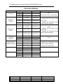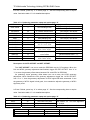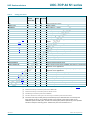
1
SERVICE MANUAL MODEL: 29M62S CHASSIS: NX56-LA 1、CAUTION: Use of controls, adjustments or procedures other than those specified herein may result in hazardous radiation exposure. CA UTION: TO REDUCE THE RISK OF ELECTRICAL SHOCK, DO NOT REMOVE COVER (OR BACK). NO USER SERVICEABLE PARTS INSIDE. REFER SER VICING TO QUALIFIED SERVICE PERSONNEL. CAUTION RISK OF ELECTRI ELECTRIC C SHOCK DO NOT OPEN. The lighting flash with arrowhead symbol, with an equilateral triangle is intended to alert the user to the presence of uninsulated dangerous voltage within the products enclosure that may be of sufficient magnitude to constitute a risk of electric shock to the person. The exclamation point within an equilateral triangle is intended to alert the user to the presence of important operating and maintenance (servicing) instructions in the literature accompanying the appliance. WARNING: TO REDUCE RISK OF FIRE OR ELECTRIC SHOCK, DO NOT EXPOSE THIS APPLIANCE TO RAIN OR MOISTURE. 2 IMPORTANT SAFETY INSTRUCTIONS CAUTION: Read all of these instructions. Save these instructions for later use. Follow all Warnings and Instructions marked on the audio equipment. 1. Read Instructions- All the safety and operating instructions should be read before the product is operated. 2. Retain Instructions- The safety and operating instructions should be retained for future reference. 3. Heed Warnings- All warnings on the product and in the operating instructions should be adhered to. 4. Follow Instructions- All operating and use instructions should be followed. FOR YOUR PERSONAL SAFETY 1. When the power cord or plug is damaged or frayed, unplug this television set from the wall outlet and refer servicing to qualified service personnel. 2. Do not overload wall outlets and extension cords as this can result in fire or electric shock. 3. Do not allow anything to rest on or roll over the power cord, and do not place the TV where power cord is subject to traffic or abuse. This may result in a shock or fire hazard. 4. Do not attempt to service this television set yourself as opening or removing covers may expose you to dangerous voltage or other hazards. Refer all servicing to qualified service personnel. 5. Never push objects of any kind into this television set through cabinet slots as they may touch dangerous voltage points or short out parts that could result in a fire or electric shock. Never spill liquid of any kind on the television set. 6. If the television set has been dropped or the cabinet has been damaged, unplug this television set from the wall outlet and refer servicing to qualified service personnel. 7. If liquid has been spilled into the television set, unplug this television set from the wall outlet and refer servicing to qualified service personnel. 8. Do not subject your television set to impact of any kind. Be particularly careful not to damage the picture tube surface. 9. Unplug this television set from the wall outlet before cleaning. Do not use liquid cleaners or aerosol cleaners. Use a damp cloth for cleaning. 10.1. Do not place this television set on an unstable cart, stand, or table. The television set may fall, causing serious injury to a child or an adult, and serious damage to the appliance. Use only with a cart or stand recommended by the manufacturer, or sold with the television set. Wall or shelf mounting should follow the manufacturer s instructions, and should use a mounting kit approved by the manufacturer. 10.2. An appliance and cart combination should be moved with care. Quick stops, excessive force, and uneven surfaces may cause the appliance and cart combination to overturn. 3 PROTECTION AND LOCATION OF YOUR SET 11. Do not use this television set near water ... for example, near a bathtub, washbowl, kitchen sink, or laundry tub, in a wet basement, or near a swimming pool, etc. Never expose the set to rain or water. If the set has been exposed to rain or water, unplug the set from the wall outlet and refer servicing to qualified service personnel. 12. Choose a place where light (artificial or sunlight) does not shine directly on the screen. 13. Avoid dusty places, since piling up of dust inside TV chassis may cause failure of the set when high humidity persists. 14. The set has slots, or openings in the cabinet for ventilation purposes, to provide reliable operation of the receiver, to protect it from overheating. These openings must not be blocked or covered. Never cover the slots or openings with cloth or other material. Never block the bottom ventilation slots of the set by placing it on a bed, sofa, rug, etc. Never place the set near or over a radiator or heat register. Never place the set in a built-in enclosure, unless proper ventilation is provided. PROTECTION AND LOCATION OF YOUR SET 15.1. If an outside antenna is connected to the television set, be sure the antenna system is grounded so as to provide some protection against voltage surges and built up static charges, Section 810 of the National Electrical Code, NFPA No. 70-1975, provides information with respect to proper grounding of the mast and supporting structure, grounding of the lead-in wire to an antenna discharge unit, size of grounding conductors, location of antenna discharge unit, connection to grounding electrode, and requirements for the grounding electrode. EXAMPLE OF ANTENNA GROUNDING AS PER NATIONAL ELECTRICAL CODE INSTRUCTIONS EXAMPLE OF ANTENNA GROUNDING AS PER NATIONAL ELECTRICAL CODE ANTENNA LEAD- IN WIRE GROUND CLAMP ANTENNA DISCHARGE UNIT (NEC SECTION 810-20) GROUNDING CONDUCTORS (NEC SECTION 810-21) ELECTRIC SERVICE EQUIPMENT GROUND CLAMPS POWER SERVICE GROUNDING ELECTRODE SYSTEM (NEC ART 250. PART H) NEC-NATIONAL ELECTRICAL CODE 15.2. Note to CATV system installer : (Only for the television set with CATV reception) This reminder is provided to call the CATV system installer s attention to Article 820-40 of the NEC that provides guidelines for proper grounding and, in particular, specifies that the cable ground shall be connected to the grounding system of the building, as close to the point of cable entry as practical. 16. An outside antenna system should not be located in the vicinity of overhead power lines or other electric lights or power circuits, or where it can fall into such power lines or circuits. When installing an outside antenna system, extreme care should be taken to keep from touching such power lines or circuits as contact with them might be fatal. 17. For added protection for this television set during a lightning storm, or when it is left unattended and unused for long periods of time, unplug it from the wall outlet and disconnect the antenna. This will prevent damage due to lightning and power-line surges. 4 OPERATION OF YOUR SET 18. This television set should be operated only from the type of power source indicated on the marking label. If you are not sure of the type of power supply at your home, consult your television dealer or local power company. For television sets designed to operate from battery power, refer to the operating instructions. 19. If the television set does not operate normally by following the operating instructions, unplug this television set from the wall outlet and refer servicing to qualified service personnel. Adjust only those controls that are covered in the operating instructions as improper adjustment of other controls may result in damage and will often require extensive work by a qualified technician to restore the television set to normal operation. 20. When going on a holiday : If your television set is to remain unused for a period of time, for instance, when you go on a holiday, turn the television set off and unplug the television set from the wall outlet. IF THE SET DOES NOT OPERATE PROPERLY 21. If you are unable to restore normal operation by following the detailed procedure in your operating instructions, do not attempt any further adjustment. Unplug the set and call your dealer or service technician. 22. Whenever the television set is damaged or fails, or a distinct change in performance indicates a need for service, unplug the set and have it checked by a professional service technician. 23. It is normal for some TV sets to make occasional snapping or popping sounds, particularly when being turned on or off. If the snapping or popping is continuous or frequent, unplug the set and consult your dealer or service technician. FOR SERVICE AND MODIFICATION 24. Do not use attachments not recommended by the television set manufacturer as they may cause hazards. 25. When replacement parts are required, be sure the service technician has used replacement parts specified by the manufacturer that have the same characteristics as the original part. Unauthorized substitutions may result in fire, electric shock, or other hazards. 26. Upon completion of any service or repairs to the television set, ask the service technician to perform routine safety checks to determine that the television is in safe operating condition. 5 TCL-Thomson Electronics R&D Center (Shen’Zhen Lab) Product Functional Specification Chassis Name Issued On Updated On NX56 2008-1-18 Serial No. Page Version 1 of 7 1.0 TTE Corporation R&D Center (Shen’Zhen Lab) Disclosure Proprietary Information: These drawings and specifications are the property of TCL-Thomson Electronics and shall not be reproduced or copied or used as the basis for the manufacture or sale of apparatus or devices without the written permission of TCL-Thomson Electronics. Version Information: Version states by two Arabic Numbers, which is separated by one dot, e.g. 1.2. The first number “1” means the version of approved file, the second one ”2” means the version of draft. Chassis Name Issued On Updated On NX-56 2008-1-18 Serial No. Page Version 2 of 7 1.0 TTE Corporation R&D Center (Shen’Zhen Lab) Revision History Model No. Status Comment V1.0 03-BA41UAE-TH32 Prepared by 29A41 Date Checked by Released by: Revised by Checked by Released by: Revised by Checked by Released by: Revised by Checked by Released by: Chassis Name Issued On Updated On NX-56 2008-1-18 Serial No. Page Version 3 of 7 1.0 TTE Corporation R D Center (Shen’Zhen Lab) Model NX-56-AP 29A41 Item Master Data -Destination 1 EM EM -Brand -BOM NO. 03-BA41UAE-TH32 -Version -Customer ID -Chassis Reception -Tuning [Channels Amt.] -Tuning [Technology] -Tuning [Indication] -Frequency Bands -IF Frequency -TV Systems (Color+ Sound) -AV Systems Picture-Processing -SCAN -Wide Screen Switching 255 PLL Digital and Bar Full Cable 38.9MHz PAL SECAM BG DK I NTSC PAL SECAM Standard -Comb filter -Picture Enhancement LTI / CTI X Black Stretch Dynamic Skin Others -Picture Control [General] X X X X X Brightness Sharpness Contrast Tint Color -Picture Control [Special] Smart Pictures * modes 7 modes VM Color Temperature 3 modes Others -Picture Noise Reduction X Picture – Display -CRT Type Normal Flat X Pure Flat Super Flat -Deflection system X 1Fh 2Fh -Tube Technology Iron X AK Black Matrix Others -CRT Deflection ( * Deg.) -CRT Magnetic Field -Screen Type -Screen Size / Vis. Size 110 4:3 29' Sound -Audio Power Consumption 5W+5W -Surround Sound Chassis: NX-56 Version: 1.0 Page 1 of 4 TTE Corporation R D Center (Shen’Zhen Lab) Model NX-56-AP 29A41 Item -Nicam -America Stereo (MTS,BTSC,MPS) -America SAP -Korea Stereo -Thai Bilingual X -Super Woofer -AVL -Sound Control [General] Volume Mute X X -Sound Control [Special] X X X Treble Bass Balance Equalizer Smart Sound * modes 7 modes Others -Speakers Quantity 2X1 User Interface -Menu Language English/Vietnam/Thai -Features [General] X AT Biological Clock Calendar Clock Channel Swap X Channel Naming Child Lock Favorite Channel X X Game Hotel Mode X High Sensitive Notebook On/Off Timer Preset Recall X X X Rotation X Sleep AVC -Features [Special] V-chip / CCD Teletext *Pages Others New Features Smart signal Voltage display X X 环境光检测 Easy search X Tuning Features -Auto Channel Program -Auto/Manual Tuning -Auto/Manual Store -Fine Tuning -Factory Mode X X X X X -Service Mode Cabinet -Cabinet Name Chassis: NX-56 Version: 1.0 Page 2 of 4 TTE Corporation R D Center (Shen’Zhen Lab) Model Item NX-56-AP 29A41 -Front Cabinet Color -Middle Cabinet Color -Rear Cabinet Color -Local Controls Front Mains Switch CH+ CH- VOL+ VOLTV/AV Menu X X X X Auto Search -Local Controls Top CH+ CH- VOL+ VOLTV/AV Menu Auto Search -Indicator RC Received LED Standby LED X X Remote Controller -Type -Batteries Connectors Rear -SCART Full w/o Y/C -SCART Full with Y/C -SCART Single (CVBS) -Component In (YPbPr) Cinch for 50Hz -In Y/C+Cinch(CVBS+ Stereo) RC166 1+2 -In Y/C+Cinch (CVBS+ Mono) -In Cinch(CVBS+ Stereo) -In Cinch (CVBS+ Mono) -Out Cinch(CVBS+ Stereo) -Out Cinch(CVBS+ Mono) - Y,Cb,Cr input -Super Woofer -Digital Audio Out -Loudspeakers -Control Busses -Feature Slot -ITV Smart Port - Antenna in 75 Ohms (IEC Type) 1(follow TV) X X Connectors Front/Side -In Y/C+Cinch(CVBS+ Stereo) -In Y/C+Cinch (CVBS+ Mono) -In Cinch(CVBS+ Stereo) -In Cinch (CVBS+ Mono) -Out Headphone Mini-Jack 3.5mm Final Equipment -Packing –Methods 2 Color Printing Carton Color -Documents and Manuals Instruction Book Screen Sticker Plastic Bag Warranty Card Chassis: NX-56 Version: 1.0 Page 3 of 4 TTE Corporation R D Center (Shen’Zhen Lab) Model Item Guarantee Doc. Warning Label Approbation Label Others -Languages DFU -Indication on BACKOVER Made-in in family sheet FCC/Elect Shock Caution Label CE/Elect Shock Caution Label Warning Label Others Approbation NX-56-AP 29A41 IEC65 Miscellaneous -Mains Voltage -Mains Frequency 100-240V 50/60Hz -Type Mains Cord -Power Consumption TV in ON -Power Consumption TV in Standby Chassis: NX-56 75W <3W Version: 1.0 Page 4 of 4 TCL Multimedia Technology Holding CRT BU R&D Center NX56-AP&NX56B-AP Chassis Alignment Procedure Disclosure Proprietary Information: These drawings and specifications are the Chassis Name NX56-AP&NX56B-AP Serial No. Issued on 2008-01-18 Page Page 1 of 17 Updated on 2009-04-24 Version 4.0 TCL Multimedia Technology Holding CRT BU R&D Center property of TCL-Thomson Electronics and shall not be reproduced or copied or used as the basis for the manufacture or sale of apparatus or devices without the written permission of TCL-Thomson Electronics. Version Information: Version states by two Arabic Numbers, which is separated by one dot, e.g. 1.2. The first number “1” means the version of approved file, the second one ”2” means the version of draft. Chassis Name NX56-AP&NX56B-AP Serial No. Issued on 2008-01-18 Page Page 2 of 17 Updated on 2009-04-24 Version 4.0 TCL Multimedia Technology Holding CRT BU R&D Center Revision History Model No. Status Prepared by 29A41/NX56 Date Luo MJ 2008-01-18 Prepared by Luo MJ 2008-01-18 Checked by Guo Guangyuan 2008-01-23 Released by Zhou Songming 2008-01-23 Prepared by Luo MJ 2008-07-04 Checked by Guo Guangyuan 2008-07-04 Released by Zhou Songming 2008-07-04 Prepared by GUO HQ 2009-02-09 Checked by Released by All NX56-AP chassis All NX56-AP chassis 14F1 21NCM86 29E64S All NX56-AP& NX56B-AP chassis Comment Ver0.1 03-BA41UAE-TH32(29A41/NX56) Ver1.0 1. Updated the B+ specs accord with 21” tube. 2. Updated the description accord with the software changing. Ver2.0 1. Updated the B+ specs accord with 25” tube. 2. Updated the description accord with the software changing. Ver3.0 Checked by Released by Zhou Songming 2009-02-09 Prepared by Luo MJ 2009-04-24 Checked by Released by Ver4.0 1. Updated the description accord with the software changing. 2. Updated the chassis name. Prepared by Checked by Released by Prepared by Checked by Released by Chassis Name NX56-AP&NX56B-AP Serial No. Issued on 2008-01-18 Page Page 3 of 17 Updated on 2009-04-24 Version 4.0 TCL Multimedia Technology Holding CRT BU R&D Center 1.1. The way to enter P-Mode a) Method one A) Switch on the TV set. B) Press the “MENU” key on RC to show the “PICTURE” OSD menu. C) Move the cursor to “Contrast” item then press the “9”, “7”, “3”, “5” key continuously on RC within 3 seconds then enter P-Mode. The “P” letter will appear on the left low corner of the screen when enter P-Mode. Also the “FACTORY HOTKEY” will be set to “ON (= 1)”. b) Another method Press the “RECALL” key on RC to enter P-mode directly. Note: 1. This will be active only when the “FACTORY HOTKEY” had set to “ON (= 1)”. 2. When the power on with “FACTORY HOTKEY” had set to “ON (= 1)”, the set will enter the P-Mode automatically. 1.2. Exit the P-Mode Press the “RECALL” or “MENU” key on RC to exit the P-Mode. 1.3. Keys’ function on RC at the P-Mode Use the RC to navigate in P-Mode: Press “0” or “AT” key for screen voltage adjustment. Press “1” to “8” and “FAV” key to select factory adjustment page. Press “9” key to switch the I2C bus off/on. Press “▲▼” or “CH+ CH-”key to select option. Press “►◄” or “VOL+ VOL-” key to adjust or select option. Press “DISPLAY” key to display software version. Press “MENU” key to close the factory menu or return to the previous menu or exit the P-Mode. Press “RECALL” key to enter or exit the P-Mode. Note: All change in P-Mode will be saved in EEPROM automatically. Chassis Name NX56-AP&NX56B-AP Serial No. Issued on 2008-01-18 Page Page 4 of 17 Updated on 2009-04-24 Version 4.0 TCL Multimedia Technology Holding CRT BU R&D Center 1.4. The adjustment page list an RC key function on P-Mode: RC key Item Description 0 Screen voltage adjustment Adjust the VG2 voltage 1 Vertical geometry Vertical geometry page 2 Horizontal geometry Horizontal geometry page 3 White Balance Adjustment 4 White Balance page Setup and option page 4 5 Setup and option page 5 6 Setup and option page select 7 Setup and option page 6 Setup and option page 7 8 Setup and option page 8 FAV Setup and option page 9 9 I2C Bus OFF/ON Press this key to enter or exit BUS OFF mode DISPLAY Software version Display software version Close menu or exit the P-Mode Close the factory menu or return to the previous menu or exit the P-Mode P-Mode hotkey Enter or exit the P-Mode Screen voltage adjustment with AKB Adjust the VG2 voltage MENU RECALL AT Chassis Name NX56-AP&NX56B-AP Serial No. Issued on 2008-01-18 Page Page 5 of 17 Updated on 2009-04-24 Version 4.0 TCL Multimedia Technology Holding CRT BU R&D Center 2. Flowchart of alignment procedure B+ adjustment Electrical properties checking for chassis RF AGC adjustment Adjustment of screen voltaget Parameter setup White balance Adjustment Aging Adjustment of focus voltage PAL geometry adjustment NTSC geometry adjustment Set shopping status QC checking 1) B+ Adjustment 2) RF AGC Adjustment 3) Screen & Focus adjustment 4) White balance adjustment 5) Producing parameter setup and option 6) Picture Geometry adjustment ( Vertical first) 7) Set Shopping status 8) QC Chassis Name NX56-AP&NX56B-AP Serial No. Issued on 2008-01-18 Page Page 6 of 17 Updated on 2009-04-24 Version 4.0 TCL Multimedia Technology Holding CRT BU R&D Center 3. Adjustment description Note: Alignment should be done after 3 minutes warm up of TV. 3.1 B+ Voltages 1. All relevant connectors and modules must be connected and inserted. 2. Main voltage is at 220VAC, 50Hz.(voltage range:110VAC~240VAC,50Hz) 3. Connect a voltmeter to B+ (Cathode of D808 for NX56 chassis or cathode of D833 for NX56B chassis) and switch on the set. 4. Input Philips test pattern signal and standard mode. 5. Adjust VR801, it should as the value in below form B+ Voltage. Table 3.1.1: The B+ value for vary tubes CRT type (Part Number) B+ Voltage A68ERF185X013/M (44-29RFLN-HFCA) 125V+/-0.5V A51ERF135X90 (44-21RFLW-HF2A) 105V+/-0.5V A51ERS357X440(44-21RFLM-HF4A) 108V+/-0.5V CRTA68AGA20X99(44-29OFLW-TS4A) 125V+/-0.5V A59EEJ04X60(44-25OFLP-HF5A) 125V+/-0.5V A59ERF181X03(44-25RFLN-HF1A) 125V+/-0.5V Chassis Name NX56-AP&NX56B-AP Serial No. Issued on 2008-01-18 Page Page 7 of 17 Updated on 2009-04-24 Version 4.0 TCL Multimedia Technology Holding CRT BU R&D Center 3.2 RF AGC alignment 3.2.1 Method 1 A. Connect the detector as shown below (Picture 3.2) to collector of Q101. B. Receive a grey scale signal with 70dBμV amplitude. C. Enter P-Mode, press “6” key on RC to select “AGCT”. D. Adjust AGCT item until the output of the detector becomes 0.8Vpp Collector of Q101 To CRO Picture 3.2 3.2.2 Method 2 A. Receive a grey scale signal with 60dBμV amplitude. B. Enter P-Mode, press “6” key on RC to select “AGCT”. C. Adjust the “AGCT” value until the hint display “AGC” just change between “0” and “1”. 3.3 Screen & Focus adjustment Note: Alignment below should be done after 15 minutes warm up of TV. 1. Input cross hatch pattern signal to RF input. 2. Enter P-Mode. 2. Press “0” key on the RC and the screen will become a horizontal line. 3. Adjust the “SCREEN” VR of the FBT until the horizontal line can just be seen barely (minimum visible intensity). 4. Press “0” key again on the RC to exit the screen voltage adjustment mode. 5. Adjust the “FCOUS” VR of the FBT until the vertical line and horizontal line becomes clear, like picture 3.3. Picture 3.3 Chassis Name NX56-AP&NX56B-AP Serial No. Issued on 2008-01-18 Page Page 8 of 17 Updated on 2009-04-24 Version 4.0 TCL Multimedia Technology Holding CRT BU R&D Center 3.4 White Balance Adjustment 1. Input a black and white pattern to RF input. 2. Enter P-Mode, press key “3” to select white balance adjustment menu. 3. Use the color analyzer to measure the black side of the screen. Adjust the value of “RC”,”GC” and “BC” to set the reading of the color analyzer to x=274, y=280. (11500 K). 4. Then measure the white side of the screen. Adjust the value of “RD”, “GD” and “BD” to set the reading of the color analyzer to x=274, y=280. (11500 K). 5. Repeat step 3&4 until you can get the correct reading for both black and white sides. Note: A. The “SubBRI” and “SubCON” items are used to assistant the white balance adjustment. It is the same function as the user OSD menu “Brightness” and “Contrast” items. You can adjust these items to get the expect intensity when adjusting the white balance. B. The “BLOR-Y”, “BLOG-Y” and “BLOB-Y” items are used for the YUV white balance black level offset setup. When the TV white balance adjustment is done, connect a black and white pattern to YUV input terminal. Use the color analyzer to measure the black side of the screen. Adjust the value of the “BLOR-Y”, “BLOG-Y” and “BLOB-Y” to set the reading of the color analyzer to x=274, y=280. Table 3.4.1: The White Balance adjustment OSD menu OSD menu Default Value Description Remark RC 32 R cut-off setting(BLOR) Adjust to right value GC 32 G cut-off setting(BLOG) Adjust to right value BC 32 B cut-off setting(BLOB) Adjust to right value RD 37 R drive setting(WPR) Adjust to right value GD 32 G drive setting(WPG) Adjust to right value BD 37 B drive setting(WPB) Adjust to right value BLOC 8 Black level offset course(BLOC) Adjust to right value accord with the tube. Recommended value= “8” PWL 8 Peak White Limiting Adjust to right value accord with the tube. Recommended value= “8” BriVSD 32 Brightness of horizontal line when adjust G2 Don’t adjust, use default value “32” for producing SubBRI 32 Brightness SubCON 32 Contrast Same as user “Brightness” and “Contrast” adjust BLOR-Y 64 BLOG-Y 62 BLOB-Y 64 BRTC 31 YUV white balance black level offset. Adjust to right value accord with the difference tube and lot Sub-Brightness See section 3.5 for detailed Chassis Name NX56-AP&NX56B-AP Serial No. Issued on 2008-01-18 Page Page 9 of 17 Updated on 2009-04-24 Version 4.0 TCL Multimedia Technology Holding CRT BU R&D Center 3.5 Sub brightness adjustment 1. Input eight steps gray signal. 2. Press key “3” to enter sub-brightness adjustment. 3. At dynamic state, adjust “BRTC” until the secondary gray bar just to be seen. (like picture 3.5.) The 2nd gray scale Picture 3.5 3.6 Picture Geometry adjustment 3.6.1 Vertical geometry adjustment 1. Input a PAL crosshatch pattern signal to RF input. 2. Enter P-Mode, press key “1” to select vertical geometry adjustment. (The OSD menu for this adjustment as below table 3.6.1. For NTSC signal, the “-50” will be replaced with “-60”.) 3. Adjust the value of the corresponding item to make the vertical geometry of the pattern look good. 4. Apply NTSC signal to adjust these value for NTSC vertical geometry. Table 3.6.1: The vertical geometry adjustment OSD menu OSD menu Default Value Description Remark VSLOPE-50 32 Vertical slope(VS) Adjust to right value VCEN-50 32 Vertical shift (VSH) Adjust to right value VSIZE-50 32 Vertical amplitude(VA) Adjust to right value VZOOM-50 25 Vertical zoom(VX) Adjust to right value VSC-50 32 S-correction(SC) Adjust to right value VSCROLL-50 32 Vertical Scroll(VCS) Adjust to right value Note: 1. For NTSC signal, the “-50” will be replaced with “-60”. 2. For NTSC signal, only the “VCEN-60” and “VSIZE-60” items need the adjustment, the other items use the same data as PAL signal. Chassis Name NX56-AP&NX56B-AP Serial No. Issued on 2008-01-18 Page Page 10 of 17 Updated on 2009-04-24 Version 4.0 TCL Multimedia Technology Holding CRT BU R&D Center 3. On producing, please use the “AUTO OFFSET” (On page “2”) function to easy the geometry adjustment of NTSC signal. When finished the PAL signal geometry adjustment, press “2” key to enter page “2” to select “AUTO OFFSET” item, press “►” key to active the automatic offset function. Then the geometry adjustment of NTSC signal will finish automated. If the geometry of NTSC signal is look good, you don’t need to adjust the geometry of NTSC signal any more. 3.6.2 Horizontal geometry adjustment 1. Input a PAL crosshatch pattern signal to RF input. 2. Enter P-Mode, press key “2” to select horizontal geometry adjustment. (The OSD menu for this adjustment as below table 3.6.2. For NTSC signal, the “-50” will be replaced with “-60”.) 3. Adjust the value of the corresponding item to make the horizontal geometry of the pattern look good. 4. Apply NTSC signal to adjust these value for NTSC horizontal geometry. Table 3.6.2: The horizontal geometry adjustment OSD menu OSD menu Default Value Description Remark HCEN-50 32 Horizontal shift(HSH) Adjust to right value HSIZE-50 32 EW width(EWW) Adjust to right value HPARA-50 32 EW parabola width(PW) Adjust to right value HTRAP-50 32 EW trapezium(TC) Adjust to right value HCNRT-50 32 EW upper corner parabola(UCP) Adjust to right value HCNRB-50 32 EW lower corner parabola(LCP) Adjust to right value HBOW-50 32 Horizontal bow(HB) Adjust to right value HPARALLEL 32 Horizontal parallelogram(HP) Adjust to right value AUTO OFFSET 0 Automatic offset NTSC geometry See below description for detailed Note: 1. For NTSC signal, the “-50” will be replaced with “-60”. 2. For NTSC signal, only the “HCEN-60” and “HSIZE-60” items need the adjustment, the other items use the same data as PAL signal. 3. On producing, please use the “AUTO OFFSET” (On page “2”) function to easy the geometry adjustment of NTSC signal. When finished the PAL signal geometry adjustment, press “2” key to enter page “2” to select “AUTO OFFSET” item, press “►” key to active the automatic offset function. Then the geometry adjustment of NTSC signal will finish automated. If now the geometry of NTSC signal is look good, it not needed to adjust the geometry of NTSC signal any more. 3.7 Producing parameter setup and option Chassis Name NX56-AP&NX56B-AP Serial No. Issued on 2008-01-18 Page Page 11 of 17 Updated on 2009-04-24 Version 4.0 TCL Multimedia Technology Holding CRT BU R&D Center 1. Enter P-Mode, press key “4” to select page “4”.Set the corresponding item to require value. See below table 3.7.1 for detailed description. Table 3.7.1: Producing parameter setup and option page “4” OSD menu Default Value Description WARM UP STATUS 0 Set aging mode SHOP INIT 0 Set the shopping status 0=>1= Set the shopping status Adjust this value to get the max color synchronization range. Don’t adjust, use default value for producing DCXO 2 Crystal oscillator frequency adjustment FACTORY HOTKEY 1 Set factory hotkey Remark 0=Aging mode off 1=Aging mode on 0=”FACTORY HOTKEY” off 1=”FACTORY HOTKEY” on ON=On when power on POWER ON MODE LAST Set the power on mode STB=Standby when power on LAST=Last power off status EEPROM INIT 0 EEPROM initial 0=>1=Active EEPROM initial POWER LOW 101 Recommended value= “16” POWER HIGH 176 Set the “Voltage display” “LOW” and “HIGH” threshold DEFAULT SND. SYS DK Set the default sound system when auto store Set the right value according to the sales area Recommended value= “168” 0= Blue background for TV and AV while no signal BLUE BACK OPT 2 Set the Background option while no signal BLACK BRI 40 Set the black background brightness while no signal BRI CURVE >> Set the brightness curve CON CURVE >> Set the contrast curve COL CURVE >> Set the colour curve VOL CURVE >> Set the volume curve 1=Black background for TV and AV while no signal 2=Snowy background for TV and black background for AV while no signal Recommended value= “20” Press “►◄” or “VOL+ VOL-” key to enter a sub-menu to do the setup, and press “MENU” key the previous menu Description: 1). Set the shopping status When trigger the “SHOP INIT” item form “0” to “1”, the TV will be put on selling status. The TV status after shopping status: A. “FACTORY HOTKEY” had set to “OFF”. Chassis Name NX56-AP&NX56B-AP Serial No. Issued on 2008-01-18 Page Page 12 of 17 Updated on 2009-04-24 Version 4.0 TCL Multimedia Technology Holding CRT BU R&D Center B. Picture set to “Standard” status. (Brightness=50, Contrast=50, Colour=50, White tone=Normal.) C. Sound set normal.(Volume=30,Balance=50.) D. 2). Set the user picture and sound curve value A. Brightness curve: OSD menu Default Value Description Remark BRI0 0 Set the minimal brightness when user Brightness=0 Set to 3 BRI50 32 Set the brightness when user Brightness=50 Use default value BRI100 63 Set the maximal brightness when user Brightness=0 B. Contrast curve: OSD menu Default Value Description Remark CON0 0 Set the minimal contrast when user Contrast=0 Set to 3 CON50 32 Set the contrast when user Contrast=50 Use default value CON100 63 Set the maximal contrast when user Contrast=0 C. Colour curve: OSD menu Default Value Description Remark COL0 0 Set the minimal colour when user Colour=0 Set to 3 COL50 32 Set the colour when user Color=50 Use default value COL100 63 Set the maximal colour when user Colour=0 D. Volume curve: OSD menu Default Value Description Remark VOL0 0 Set the volume when user Volume=0 Use default value VOL10 38 Set the volume when user Volume=10 VOL30 65 Set the volume when user Volume=30 Set to 63 VOL50 71 Set the volume when user Volume=50 Set to 69 VOL80 77 Set the volume when user Volume=80 Set to 75 VOL100 83 Set the volume when user Volume=100 Set to 81 3). Set the value for “POWER LOW” and “POWER HIGH” A. Connect the main voltage at low threshold 95VAC/50Hz. B. Select item “POWER LOW”. C. Adjust the value until the hint display just change between “AC: NORMAL” and “AC: LOW”. D. Connect the main voltage at high threshold 255VAC/50Hz. E. Select item “POWER HIGH. F. Adjust the value until the hint display just change between “AC: NORMAL” and “AC: HIGH”. Chassis Name NX56-AP&NX56B-AP Serial No. Issued on 2008-01-18 Page Page 13 of 17 Updated on 2009-04-24 Version 4.0 TCL Multimedia Technology Holding CRT BU R&D Center 2. Enter P-Mode, press key “5” to select page “5”. Set the corresponding item to require value. See below table 3.7.2 for detailed description. Table 3.7.2: Producing parameter setup and option page “5” OSD menu Default Value Description Remark Track. Mode 1 EHT tracking mode VX Normal 25 4:3 mode vertical zoom Don’t adjust, use default VX Compr. 0 16:9 mode vertical zoom Don’t adjust, use default WBF 5 Wide blanking start Don’t adjust, use default WBR 8 Wide blanking end Don’t adjust, use default GET OFFSET 0 Get offset See below description for detailed ColdRC 61 Recommended value= “61” ColdGC 56 Cold color temperature R and G cut-off offset ColdRD 61 ColdGD 66 WarmRC 72 WarmGC 71 WarmRD 65 WarmGD 64 0=EHT tracking only on vertical 1=EHT tracking on vertical and EW Recommended value= “56” Recommended value= “61” Cold color temperature R and G drive offset Recommended value= “66” Recommended value= “72” Warm temperature R and G cut-off offset Recommended value= “71” Recommended value= “65” Warm color temperature R and G drive offset Recommended value= “64” Description for AUTO OFFSET and GET OFFSET: The “GET OFFSET” can use to make the EEPROM copy by PE engineer. When the PAL and NTSC geometry adjustment had finished, trigger the “GET OFFSET” from “0” to “1” to store the geometry offset datum between PAL and NTSC in EEPROM. On producing, these geometry offset datum can use to easy the NTSC geometry adjustment. When finished the PAL geometry adjustment, trigger the “AUTO OFFSET” from “0” to “1”, then the geometry adjustment of NTSC signal will finish automated. If now the geometry of NTSC signal is look good, it not needed to adjust the geometry of NTSC signal any more. 3. Enter P-Mode, press key “6” to select page “6”. Set the corresponding item to require value. See below table 3.7.3 for detailed description. Table 3.7.3: Producing parameter setup and option page “6” OSD menu Default Value Description AGCT 32 AGC take over point AGC 0 AGC take over point indicate OIF 32 IF demodulator offset Remark See section “3.2 for detailed. RF AGC alignment” Don’t adjust, use default Chassis Name NX56-AP&NX56B-AP Serial No. Issued on 2008-01-18 Page Page 14 of 17 Updated on 2009-04-24 Version 4.0 TCL Multimedia Technology Holding CRT BU R&D Center IF 38.90 IF frequency Select the IF frequency AGCS 1 AGC speed Don’t adjust, use default AGNE 3 Audio gain Don’t adjust, use default 4. Enter P-Mode, press key “7” to select page “7”. Set the corresponding item to require value. See below table 3.7.4 for detailed description. Table 3.7.4: Producing parameter setup and option page “7” OSD menu Default Value Description Remark EVG 0 Enable vertical guard(RGB blanking) 1= RGB blanking DFL 0 Disable flash protection from deflection timer Don’t adjust, use default XDT 0 X-ray detection Don’t adjust, use default AKB 1 Black current stabilization Don’t adjust, use default NBL 1 Black current loop application Don’t adjust, use default OSVE 0 Black current measuring lines in over scan(for vertical zoom setting <1) Don’t adjust, use default CL 8 Set the cathode drive level Adjust to right value accord with the tube. Recommended value= “12” NTSCM 0 RF NTSC M enable NTSC443 0 AV NTSC443 enable ONE SPEAK 0 Mono speaker output setup (Note: this item is available on AP3 version) 0=Disable 1= Enable 0=Stereo speaker 1=Mono speaker 5. Enter P-Mode, press key “8” to select page “8”. Set the corresponding item to require value. See below table 3.7.5 and table 3.7.6 for detailed description. Table 3.7.5: Producing parameter setup and option page “8”(For AP2 version) OSD menu Default Value Description Remark HOTEL 0 Hotel mode enable A2 THAI 1 Thailand dual language enable PIC PRESET 1 Picture preset enable AV ALIGMENT 1 Rear AV terminal align SHVS ENABLE 1 S-Video terminal enable YUV ENABLE 1 YUV terminal enable NOCOMMAND ENABLE 0 No operation within 2 hours automatic standby enable ARABIC* 1 Arabic enable Chassis Name NX56-AP&NX56B-AP Serial No. Issued on 2008-01-18 Page Page 15 of 17 Updated on 2009-04-24 Version 4.0 0=Disable 1= Enable 0=3 x 3 1=4 x 3 0=Disable 1=Enable TCL Multimedia Technology Holding CRT BU R&D Center RUSSIAN* 1 Russian enable FRENCH* 1 French enable FARSI* 1 Farsi enable TUNER TYPE* 1 Select tuner type 0=ALPS tuner 1=TCL tuner AV STANDB 0 AV no signal within 10 minutes automatic standby AVOUT FOLLOW 0 AV output source follow 0=Disable 1=Enable 0=Follow TV 1=Follow source Table 3.7.6: Producing parameter setup and option page “8”(For AP3 version) OSD menu Default Value Description Remark HOTEL 0 Hotel mode enable A2 THAI 1 Thailand dual language enable HEALTH FLAT 1 Health platform TV enable AC DISPLAY 1 AC voltage checking enable AV ALIGMENT 1 Rear AV terminal align AV2 ENABLE 1 AV2 input enable SHVS ENABLE 1 S-Video terminal enable YUV ENABLE 1 YUV terminal enable NOCOMMAND ENABLE 0 No operation within 2 hours automatic standby enable THAI* 1 Thai enable VIET* 1 Vietnamese enable TUNER TYPE* 1 Select tuner type 0=Disable 1= Enable 0=3 x 3 1=4 x 3 0=Disable 1=Enable 0=ALPS tuner 1=TCL tuner AV STANDB 0 AV no signal within 10 minutes automatic standby AVOUT FOLLOW 0 AV output source follow 0=Disable 1=Enable 0=Follow TV 1=Follow source *Note: When change the Language or the tuner type, you must AC restart the TV set to make it active. 6. Enter P-Mode, press key “FAV” to select page “9”. Set the corresponding item to require Chassis Name NX56-AP&NX56B-AP Serial No. Issued on 2008-01-18 Page Page 16 of 17 Updated on 2009-04-24 Version 4.0 TCL Multimedia Technology Holding CRT BU R&D Center value. See below table 3.7.7 for detailed description. Table 3.7.7: Producing parameter setup and option page “9” OSD menu Default Value Description BKS 1 Black stretch enable BSD 0 Black Stretch depth Remark 0=Disable 1=Enable 0=15IRE 1=30IRE 0=12% AAS 0 Black area to switch off the black stretch 1=20% 2=6% 3=8% 0=1:1 RPA 1 Ratio of pre- and after shoot 1=1.5:1 2=2:1 0=1:1 RPO Ratio of positive and negative peaks 1 1=1:1.3 3=1:1.7 4=1:0.7 0=0% SOC Soft clipping level above PWL 2 1=5% 2=10% 3=Soft clipping off 0=off COR 0 Video peaking active range 1= between 0 and 20 IRE 2= between 0 and 40 IRE 3= between 0 and 100 IRE 3.8 Screen voltage (VG2) adjustment with AKB function 1. Put the TV in AV source without input signal. 2. Enter P-Mode, press RC key "AT", there will display 3. Adjust the "SCREEN" VR of the FBT until VG2 hint display (LOW/OK/HIGH) display "OK" stably. 4. Press “MENU” return to P-Mode. Chassis Name NX56-AP&NX56B-AP Serial No. Issued on 2008-01-18 Page Page 17 of 17 Updated on 2009-04-24 Version 4.0 Chapter II 220VAC INPUT ▽ Block Diagram of NX56 Bridge Rectifier DB801DB804 Antenna July5,2008 Power Transistor Q801 2SK2996 Transformer T801 IC801 NCP1337 Photo-Coupler IC803 B 33V +-14V 12V 9V Q501 Q503 Q505 AMP CRT R/G/B P201 Tuner TU101 IF AMP Q101 V.AMP. IC301 STV8172A SAW Z2O1 Pin44-46 Pin14/15 VDA/B SCA/SDL EEPROM IC001 H.Driver AMP Q401 Q402 Pin 56 H.OUT UOC IC201 P901 TV/AV/SV B+ P202 pin21 IC701 AN5832SA Aout KEY &IR001 SENSOR -L/R IC702 74HC4053 Audio AMP. IC601 TDA7266SA 200V FBT T401 24V 6.3V speakerX2 NX56 Chassis Signal Processing Introduction Brief introduction For different market requirements, our design it in two versions, one is for Latin America, we call the chassis as NX56-LA, the another one is for Asia Pacific Area, we call the chassis as NX56-AP. NX56-LA and NX56-AP adopt different UOC, The UOC for Latin America have CCD-Chip and BTSC function, so added AN5832SA to realize BTSC, but the UOC for Asia Pacific region does not have the two functions but SECAM system is necessary. NX56 Chassis not only match 21inches CRT, but also match 25 and 29inches CRT. Due to different screen sizes, maybe adopt different audio power amplifiers. The others should be the same. No matter NX56-AP what NX56-LA, they are use same main PCB board, just different peripheral components. RF Section Tuner Tu101 receive the radio frequency signal, after inside circuit to do signal receiving, and signal amplifying. The amplified high frequency signal accompany with the high frequency oscillation voltage oscillated by set oscillator input to the mixer. The IF picture signal and sound signal formed in mixer and output from mixer, then send to picture IF processing circuit. VGA (Fig. 1. Tuner section) Small Signal Processing Section Small signal processing section is the IF (intermediate frequency) signal across saw filter send in the pin12 and pin13 of IC201. The VIFIN signal through built-in PLL DEMOD, sound trap, video amplifier and synchronous detector processing, get the color video broadcast signal and 2nd sound IF signal. Video signal processing section is CVBS across video filter and delay line and horizontal & vertical synchronous separation circuit processing and get H-drive (pin56 of IC201)and V-drive signal (pin15/pin15 of IC201). IF sound signal across the sound-down-mixer and AM demodulator processing, send out the AVL/ SSIF OUT signal. ( Refer to Fig2 and Fig 3.) (Fig 2. Small Signal Processing Section) (Fig3. Block Diagram of IC201.) Horizontal Scanning Section The horizontal drive signal send out from pin 56 of IC201, Q401 is horizontal driving transistor, coupled by horizontal driving transformer T402 , to control the horizontal output transistor working in switch on and off situation, get good linearly and enough amplitude of saw-tooth wave current to drive horizontal deflection yoke scanning. L456 is horizontal width coil and L458 is horizontal linearly coil. D455 is damping diode, C453,C455,C457 are retrace capacitors. T401 is FBT. Pin2 of T401 is B+ voltage input, Pin 10 of T401 get 200 Volt video amplifying voltage supply for CRT board. Pin11 of T401 sends out heater voltage supply for CRT heater. Vertical Scanning Section Vertical scanning section adopted STV8172A vertical deflection booster, we use as differential-output driver. The vertical raw-tooth wave signal sends out from pin14/15 of IC201 VDA/VDB. The two differential signal input pin 1 and 7 of STV8172A IC301. Pin2(+14v) and Pin7(-14v) of IC301 is power supply which come from the main power transformer. Pin 6 is boost voltage, rectified by D301. C309,C301 and R305 makes up a voltage feedback network, R306 is a damping resistor. C306 is correction capacitor, R308 is current feedback resistor. Fig 4. Vertical Scanning Processing Section CRT Scanning Section Q507,D501,D502 and D503 makes up a light eliminate circuit network. When the TV is playing mode, +8V voltage across R533 charge for C512, Q507 is cut off. At the right of turn off the TV, Q507 is turn-on, the current across D501, D502 and D503 send to R.G. B to discharge the electronic quickly. Audio Power Amplifying Section Power Supply Section AC supply 220V/110v through filtering network and rectifying circuit and get 300Vdc voltage. LF801/LF801A and CX802 makes up a differential mode rejection, LF802 and CY801,CY802 makes up a common mode rejection network. D801-D804 is rectifying network. 300Vdc voltage supply pin3 of T801, also through R804 send to pin8 of IC801 NCP1337. Pin5 of IC801 sends out the PWM signal to control Q801 working in switch on and off situation. IC803 is optocoupler. UOC-TOP-64 N1 series Versatile signal processor for CRT TV applications Rev. 0.11 — 25 January 2007 Product data sheet 1. General description The UOC-TOP-64 series is a very flexible concept which offers attractive solutions for 1fH TV receivers with CRTs. This new concept offers a complete range of products with the right price level to cover TV receivers from basic mono 14 inch sets up to the best featured large and/or wide screen AV-stereo TV sets. The UOC-TOP-64 concept can also be used as front-end for 2fH and LCD TV receivers. The UOC-TOP-64 concept is mounted in a SDIP64 package and is split up in the following ranges: • AV-110 (AV-stereo) concept. It contains a video processor with many features and it has an analog audio control circuit with balance, treble, bass and loudness control. Two different micro processor are available for this concept, one with OSD and Closed Captioning or Teletext and Closed Captioning features (UOCTOP_1PTXT version), the other with (extended) OSD features (UOCTOP_OSD version). The block diagram is given in Figure 1. • AV-90 concept. This concept is nearly identical to the AV-110 concept. The only difference that it does not contain an East-West and Scan Velocity Modulation (SVM) output. This concept is intended for 90× picture tubes. • Mono-110 concept. The functional content of this concept is comparable with that of the AV 110 concept, however, it has just stereo input switch and no audio control circuit. The block diagram is given in Figure 1. • Mono-90 concept. This concept is intended for 90× picture tubes. The circuit has an audio switch for mono signals but the mono inputs can also be used as a stereo input. In this range most of the video and audio processing features have been omitted. Also this concept can be supplied with one of the two micro processors (UOCTOP_1PTXT or UOCTOP_OSD version). The block diagram is given in Figure 2. The most important features of the complete IC series are given in the following feature lists. All packages are according to the ROHS legislation, which also means that these packages are lead-free. The ICs have supply voltages of 8V, 5V and 3.3V. UOC-TOP-64 is supported by a comprehensive Global TV Software Development kit to enable easy programming and fast time-to-market (see also Section 20.4 “Licenses”). UOC-TOP-64 N1 series NXP Semiconductors Signal processor for CRT TV 2. Features 2.1 Analog Video Processing 2.1.1 Overview of available features (AV-110/90 and Mono-110 concept) Multi-standard vision IF circuit with alignment-free PLL demodulator Internal (switchable) time-constant for the IF-AGC circuit Switchable group delay correction and sound trap (with switchable centre frequency) for the demodulated CVBS signal Separate Second Sound IF output or FM demodulator output without de-emphasis available, which can be used as input for an external BTSC decoder or as input for external sound band-pass filter for second language processing. Separate SSIF input available as input for the FM-PLL demodulator to demodulate FM-radio with an IF frequency of 10.7 MHz, or as input from an external sound band-pass filter for second language processing. AM demodulator without extra reference circuit The mono intercarrier sound circuit has a selective FM-PLL demodulator which can be switched to the different FM sound frequencies (4.5/5.5/6.0/6.5 MHz). The quality of this system is such that the external band-pass filters can be omitted. The FM-PLL demodulator can be set to centre frequencies of 4.72/5.74 MHz so that a second sound channel can be demodulated. In such an application it is necessary that an external bandpass filter is inserted. Audio switch circuit with 2 stereo inputs (1 stereo input can also be switched into two mono sound inputs) and a stereo output which can be used for the drive of for audio power amplifiers (with volume and tone-control) or as SCART/CINCH output. The second stereo input is only available via the combined C2/C3/C4/AUDIOIN5R pin for the right channel and via the combined CVBS4/Y4/AUDIOIN5L pin for the left channel. Video switch with 3 external CVBS inputs. All CVBS inputs can be used as Y-input for Y/C signals. However, only 1 Y/C source can be selected because the circuit has 1 chroma input. CVBS3/Y3 input available in combination with the G/Y-3 input pin. 1 CVBS output, this output can be used as monitor video output or as front-end video output or as independent selectable video output. Automatic Y/C signal detector. Integrated luminance delay line with adjustable delay time Only one reference (24.576 MHz) crystal required for the m-Controller, Teletext- and the color decoder Multi-standard color decoder with automatic search system and various “forced mode” possibilities Internal base-band delay line Indication of the Signal-to-Noise ratio of the incoming CVBS signal Linear RGB/YPBPR input. Scan Velocity Modulation output. The SVM circuit is active for all the incoming CVBS, Y/C and RGB/YPBPR signals. The SVM output is combined with the black current input of the black current stabilisation circuit. By means of a small application adaptation both functions can be operational in parallel. <Document ID> Product data sheet © NXP B.V. 2007. All rights reserved. Rev. 0.11 — 25 January 2007 2 of 230 NXP Semiconductors UOC-TOP-64 N1 series Signal processor for CRT TV Picture improvement features with peaking (with switchable centre frequency, depeaking, variable positive/negative peak ratio, variable pre-/overshoot ratio and video dependent coring), dynamic skin tone control, gamma control and blue- and black stretching. All features are available for CVBS, Y/C and RGB/YPBPR signals The effect of the various features can de demonstrated by means of a ‘split screen’ mode in which the features are activated in one half of the picture and switched off in the other half Switchable DC transfer ratio for the luminance signal Tint control for external RGB/YPBPR signals Contrast reduction possibility during mixed-mode of OSD and Text signals. Option to make a colored and in contrast reduced window. RGB control circuit with ‘Continuous Cathode Calibration’, white point and black level off-set adjustment so that the color temperature of the dark and the light parts of the screen can be chosen independently. When this ‘Continuous Cathode Calibration’ is not used, simple alignment of the cutoff level is possible. Adjustable ‘wide blanking’ of the RGB outputs Horizontal synchronization with two control loops and alignment-free horizontal oscillator Vertical count-down circuit Vertical driver optimized for DC-coupled vertical output stages Horizontal and vertical geometry processing with horizontal parallelogram and bow correction and horizontal and vertical zoom The IC can be used as front-end for Progressive Scan or LCD TV receivers Low-power start-up of the horizontal drive circuit 2.1.2 Features of the AV-110/90 concept which are not available in the Mono-110 concept Analog audio tone control circuit with treble, bass and loudness controls 2.1.3 Features of the AV-110 and Mono-110 concept which are not available in the AV-90 concept Horizontal geometry processing and Scan Velocity Modulation output 2.1.4 Differences in feature list for the MONO-90 concept compared with AV-110/90 and Mono-110 concept Audio switch circuit with 1 stereo input, which can also be switched into two mono sound inputs, a mono output for SCART/CINCH with the possibility to serve as front/monitor audio output. Stereo output (with volume and AVL) for audio power amplifiers. This stereo output can also be switched to one mono loudspeaker output and one fixed mono sound output. CVBS output, this output can only be used as monitor video output or as front-end video output. Only basic video processing. The remaining video features are peaking with coring, black stretching and gamma control. No horizontal geometry processing and Scan Velocity Modulation output. <Document ID> Product data sheet © NXP B.V. 2007. All rights reserved. Rev. 0.11 — 25 January 2007 3 of 230 NXP Semiconductors UOC-TOP-64 N1 series Signal processor for CRT TV 2.2 Micro-Controller 80C51 m-controller core standard instruction set and timing 0.9766 ms machine cycle maximum of 80 k x 8-bit late programmed ROM maximum of 3 k x 8-bit Auxiliary RAM I2C byte level bus interface. Interrupt controller for individual enable/disable with two level priority Two 16-bit Timer/Counter registers One 24-bit Timer (16-bit timer with 8-bit Pre-scaler) 16-bit Data pointer WatchDog timer Auxiliary RAM page pointer Stand-by, Idle and Power Down modes Up to 13 general-purpose I/O pins 14 bits PWM for Voltage Synthesis Tuning 8-bit A/D converter with 4 multiplexed inputs 4 PWM (6-bits) outputs for analogue control functions 2.3 Data Capture (Teletext and Closed Caption devices) Text memory for 1 page Inventory of transmitted Teletext pages stored in the Transmitted Page Table (TPT) and Subtitle Page Table (SPT) Data Capture for US Closed Caption Data Capture for 525/625 line WST, VPS (PDC system A) and 625 line Wide Screen Signalling (WSS) bit decoding Automatic selection between 525 WST/625 WST Automatic selection between 625 WST/VPS on line 16 of VBI Real-time capture and decoding for WST Teletext in Hardware, to enable optimized m-processor throughput Automatic detection of FASTEXT transmission Real-time packet 26 engine in Hardware for processing accented, G2 and G3 characters Signal quality detector for video and WST/VPS data types Comprehensive teletext language coverage Vertical Blanking Interval (VBI) data capture of WST data <Document ID> Product data sheet © NXP B.V. 2007. All rights reserved. Rev. 0.11 — 25 January 2007 4 of 230 UOC-TOP-64 N1 series NXP Semiconductors Signal processor for CRT TV 2.4 Display 2.4.1 Features of the OSD-only devices Up to 4 character sets with 256 characters each (size 16 pixels x 18 lines) Enhanced OSD modes 50Hz/60Hz display timing modes Serial and Parallel Display Attributes Single/Double Width and Height for characters Scrolling of display region Variable flash rate controlled by software Enhanced display features including overlining, underlining and italics Soft colors using CLUT with 4096 color palette Global selectable matrix: (12/16) By attribute selectable: 1.5x characters (18/24) Globally selectable character spacing Fringing (Shadow) selectable from N-S-E-W direction Fringe color selectable Contrast reduction of defined area with option of coloration Programmable Cursor Special Graphics Characters with two planes, allowing four colors per character 2.4.2 Features of the Teletext and Closed Caption devices Four character sets Up to 576 characters with a size of 12 pixels x 16 lines are supported Teletext and Enhanced OSD modes 50Hz/60Hz display timing modes Serial and Parallel Display Attributes Scrolling of display region Variable flash rate controlled by software Soft colors using CLUT with 4096 color palette Global selectable matrix: (12) Features of level 1.5 WST and US Close Caption Single/Double/Quadruple Width and Height for characters 64 software redefinable On-Screen display characters G1 Mosaic graphics, Limited G3 Line drawing characters WST Character sets and Closed Caption Character set in single device Curtaining effect via software Fringing (Shadow) selectable from N-S-E-W direction Fringe color selectable Contrast reduction of defined area with option of coloration Programmable Cursor Special Graphics Characters with two planes, allowing four colors per character <Document ID> Product data sheet © NXP B.V. 2007. All rights reserved. Rev. 0.11 — 25 January 2007 5 of 230 UOC-TOP-64 N1 series NXP Semiconductors Signal processor for CRT TV 3. Quick reference data Table 1: Quick reference data SYMBOL PARAMETER MIN. TYP. MAX. UNIT VP analogue supply voltage VSP 4.7 5.0 5.3 V IP supply current (5.0 V) − 160 − mA VDDA digital supply VSP / analogue supply periphery 3.0 3.3 3.6 V IDDA supply current (3.3 V); Mono90 version − 50 − mA IDDA supply current (3.3 V); AV110/90 and Mono110 versions − 70 − mA VPAudio[1] audio supply voltage 4.7 8.0 8.4 V IPAudio[1] supply current (5.0/8.0 V); mono-90 version − 0.5 − mA IPAudio supply current (8.0 V); AV-110/90 and mono-110 version − 10 − mA Ptot total power dissipation − − 1.1 W ViVIFrms) video IF amplifier sensitivity (RMS value) − 75 150 µV ViSSIF(rms) sound IF amplifier sensitivity (RMS value) − 1.0 − mV Supply Input voltages ViAUDIO(rms) external audio input (RMS value) − 1.0 1.3 V ViCVBS(p-p) external CVBS/Y input (peak-to-peak value) − 1.0 1.4 V ViCHROMA(p-p) external chroma input voltage (burst amplitude) (peak-to-peak value) − 0.3 1.0 V ViRGB(p-p) RGB inputs (peak-to-peak value) − 0.7 0.8 V ViY(p-p) luminance input signal (peak-to-peak value) − 1.0 − V ViPB(p-p) PB input signal (peak-to-peak value)[2] − 0.7 − V ViPR(p-p) value)[2] − 0.7 − V PR input signal (peak-to-peak Output signals Vo(IFVO)(p-p) demodulated CVBS output (peak-to-peak value) − 2.0 − V Vo(QSSO)(rms) sound IF intercarrier output (RMS value) − 100 − mV Vo(AMOUT)(rms) demodulated AM sound output (RMS value) − 250 − mV Vo(AUDIO)(rms)[1] non-controlled audio output signals (RMS value) 1.0 − − V Vo(CVBSO)(p-p) selected CVBS output (peak-to-peak value) − 2.0 − V Io(AGCOUT) tuner AGC output current range 0 − 1 mA VoRGB(p-p) RGB output signal amplitudes (peak-to-peak value) − 1.2 − V IoHOUT horizontal output current 10 − − mA IoVERT vertical output current (peak-to-peak value) − 1 − mA IoEWD EW drive output current − − 1.2 mA [1] The supply voltage for the analogue audio part of the mono-90 version can be 5V or 8V. For a supply voltage of 5V the maximum signal amplitudes at in and outputs are 1Vrms. For a supply voltage of 8V the maximum output signal amplitude is 2 Vrms. The AV-110/90 and Mono-110 versions need a supply voltage of 8 V. [2] The YPBPR input signal amplitudes are based on a color bar signal with 100% saturation. <Document ID> Product data sheet © NXP B.V. 2007. All rights reserved. Rev. 0.11 — 25 January 2007 6 of 230 Fig 1. Product data sheet CVBS4/Y4 AUDIOIN5L C2/C3/C4/ AUDIOIN5R CVBS2/Y2 YSYNC VIFIN AGCOUT IFVO/SVO/PIP <Document ID> Rev. 0.11 — 25 January 2007 H-OSC. + PLL 2nd LOOP H-SHIFT H-DRIVE H/V SYNC SEP. VIDEO FILTERS VIDEO SWITCH VIDEO IDENT. H/V H-OUT VISION IF/AGC/AFC PLL DEMOD. SOUND TRAP GROUP DELAY VIDEO AMP. SOUND-DOWNMIXER EHTO REF // R RGB/YPRPB SWITCH AM FM B3/ PB-3 GAMMA CONTROL BRI CON. U/V TINT SATURATION RGB MATRIX BLUE/BLACK-STRETCH SKIN TONE AVL LS AUDIO OUTPUT VOLUME/TONE**) CONTROL SAT G3/ Y-3 EWD/AVL R3/ CVBS3/ PR-3/ Y3 C2/C3/C4 V-DRIVE GEOMETRY & EAST-WEST VERTICAL Y DELAY ADJ. DELAY LINE BASE-BAND DECODER PAL/SECAM/NTSC DEEMPHASIS SOUND PLL SECAM L LS/SCART/CINCH -OUT /// CLKI // RO/ GO/ BO/ PR Y PB IREFO RGB CONTROL OSD/TEXT INSERT /// CONTR/BRIGHTN INS. CCC/BLACK ADJ. CIRN WHITE-P. ADJ. CSO // H/VDISPO MODULATION SCAN VELOCITY PEAKING I2C-BUS RESET CLK GENERATION AUDIO SELECT SCART/CINCH IN IREF CORB VDS R/G/B IREFRGB H/VDISPI CSI CVBS IN CVBSREF SDA/SCL TMSEL CLKO I/Os 5. AM DEMODULATOR AVL/SSIFOUT/FMDEMOUT NXP Semiconductors UOC-TOP-64 N1 series Signal processor for CRT TV Block diagram µ-PROCESSOR / TELETEXT DECODER / OSD BCLIN BLKIN/SVM/ VGUARD **) The mono-110 version has only volume control and no tone control functions Block diagram of the “AV-110/90” and “MONO-110” TV processor © NXP B.V. 2007. All rights reserved. 9 of 230 Fig 2. Product data sheet CVBS4/Y4 C2/C3/C4/ CVBS2/Y2 YSYNC VIFIN AGCOUT IFVO/SVO <Document ID> Rev. 0.11 — 25 January 2007 H-OSC. + PLL 2nd LOOP H-SHIFT H-DRIVE H/V SYNC SEP. VIDEO FILTERS VIDEO SWITCH VIDEO IDENT. H/V H-OUT VISION IF/AGC/AFC PLL DEMOD. SOUND TRAP GROUP DELAY VIDEO AMP. SOUND-DOWNMIXER AM DEMODULATOR AVL/SSIFOUT/FMDEMOUT V-DRIVE VERTICAL Y DELAY ADJ. DELAY LINE BASE-BAND DECODER REF // L AVL RGB/YPRPB SWITCH SAT B3/ PB-3 GAMMA CONTROL BLACK-STRETCH RGB MATRIX SATURATION LS AUDIO OUTPUT VOLUME/AVL CONTROL G3/ Y-3 R3/ CVBS3/ PR-3/ Y3 C2/C3/C4 EHTO PAL/SECAM/NTSC DEEMPHASIS SOUND PLL SECAM LS/SCART/CINCH -OUT BRI CON. AM FM /// CLKI // RO GO BO IREFO RGB CONTROL OSD/TEXT INSERT /// CONTR/BRIGHTN INS. CCC/BLACK ADJ. CIRN WHITE-P. ADJ. CSO // H/VDISPO CORING PEAKING I2C-BUS RESET CLK GENERATION AUDIO SELECT SCART/CINCH IN IREF CORB VDS R/G/B IREFRGB H/VDISPI CSI CVBS IN CVBSREF SDA/SCL TMSEL CLKO I/Os NXP Semiconductors UOC-TOP-64 N1 series Signal processor for CRT TV µ-PROCESSOR / TELETEXT DECODER / OSD BCLIN BLKIN/VGUARD Block diagram of the “MONO-90” TV processor © NXP B.V. 2007. All rights reserved. 10 of 230 UOC-TOP-64 N1 series NXP Semiconductors Signal processor for CRT TV 6. Pinning information Table 6: Pinning information SYMBOL IFVO/SVO/PIP [3] IFVO/SVO [3] VP2 VCC8V PLLIF GND2 DECSDEM AVL/SSIFOUT/SNDDEMOUT[2] EHTO AGCOUT IREF VSC VIFIN2 VIFIN1 VDRA VDRB EWD/AVL AVL DECBG SECPLL GND1 PH1LF PH2LF VP1 DECDIG XTALOUT XTALIN P1.5 P3.3/ADC3/PWM3 P3.2/ADC2/PWM2 P3.1/ADC1/PWM1 P3.0/ADC0/PWM0 P2.1/PWM0 P2.0/TPWM VDDP(3.3V) P1.7/SDA P1.6/SCL P1.3/T1 P1.1/T0 P1.0/INT1 INT0/P0.5 AV-110 Mono-110 1 − 2 3 4 5 6 7 8 9 10 11 12 13 14 15 16 − 17 18 19 20 21 22 23 24 25 26 27 28 29 30 31 32 33 34 35 36 37 38 39 VDDC(3.3V) 40 SDIP64 DESCRIPTION AV-90 Mono-90 1 − 2 3 4 5 6 7 8 9 10 11 12 13 14 15 − 16 17 18 19 20 21 22 23 24 25 26 27 28 29 30 31 32 33 34 35 36 37 38 39 − 1 2 3 4 5 6 7 8 9 10 11 12 13 14 15 − 16 17 18 19 20 21 22 23 24 25 26 27 28 29 30 31 32 33 34 35 36 37 38 39 40 40 IF video output / selected CVBS output / PIP output IF video output / selected CVBS output 2nd supply voltage TV processor (+5 V) 8 Volt supply for audio switches IF-PLL loop filter ground 2 for TV processor decoupling sound demodulator AVL / Second sound IF output / sound demodulator output EHT/overvoltage protection input tuner AGC output reference current input vertical sawtooth capacitor IF input 2 IF input 1 vertical drive A output vertical drive B output East-West drive output / AVL capacitor AVL capacitor bandgap decoupling SECAM PLL decoupling ground 1 for TV-processor phase-1 filter phase-2 filter 1st supply voltage TV-processor (+5 V) decoupling digital supply crystal oscillator output crystal oscillator input port 1.5 port 3.3 or ADC3 input or PWM3 output port 3.2 or ADC2 input or PWM2 output port 3.1 or ADC1 input or PWM1 output port 3.0 or ADC0 input or PWM0 output port 2.1 or PWM0 output port 2.0 or Tuning PWM output supply to periphery (3.3V) port 1.7 or I2C-bus data line port 1.6 or I2C-bus clock line port 1.3 or Counter/Timer 1 input port 1.1 or Counter/Timer 0 input port 1.0 or external interrupt 1 external interrupt 0 or port 0.5 (4 mA current sinking capability for direct drive of LEDs) supply <Document ID> Product data sheet © NXP B.V. 2007. All rights reserved. Rev. 0.11 — 25 January 2007 11 of 230 UOC-TOP-64 N1 series NXP Semiconductors Signal processor for CRT TV Table 6: Pinning information SYMBOL GND5 VPE VDDA1(3.3V) BO/PBOUT BO GO/YOUT GO RO/PROUT RO BLKIN/VGUARD/SVM [1][6] AV-110 Mono-110 41 42 43 44 − 45 − 46 − 47 BLKIN/VGUARD [1][6] BCLIN B3/PB3 G3/Y3/CVBS3/Y3 [1] R3/PR3/C2/C3/C4 [1] YOUT YSYNC VP3 GND3 HOUT FBISO/SANDCA AUDOUTSM2/LSR SDIP64 DESCRIPTION AV-90 Mono-90 41 42 43 44 − 45 − 46 − − 41 42 43 − 44 − 45 − 46 − − 48 49 50 51 52 53 54 55 56 57 58 47 48 49 50 51 52 53 54 55 56 57 58 47 48 49 50 51 52 53 54 55 56 57 58 AUDOUTLSM1/LSL 59 59 59 C2/C3/C4/AUDIOIN5R [1] C2/C3/C4 AUDIOIN3/IN1R [5] CVBS2/Y2 AUDIOIN2/IN1L/SSIF [4][5] CVBS4/Y4/AUDIOIN5L [1] CVBS4/Y4 60 − 61 62 63 64 − 60 − 61 62 63 64 − 60 61 62 63 − 64 ground OTP Programming Voltage supply voltage Blue output / PB output Blue output Green output / Y output Green output Red output / PR output Red output black current input / vertical guard / scan velocity modulation output black current input / vertical guard beam current limiter input 3rd B input / PB input 3rd G input / Y input / CVBS input / Y input 3rd R input / PR input / C2/3/4 input Y-output (for YUV interface) Y-input for sync separator supply voltage (5 V) ground connection horizontal output flyback input/sandcastle output audio output for audio power amplifier (right signal) or fixed audio output for mono applications audio output for audio power amplifier (left signal) or speaker output for mono applications chroma-2/3/4 input / audio 5 right input chroma-2/3/4 input audio 3 input / right stereo input CVBS2/Y2 input audio 2 input / left stereo input / sound IF input CVBS4/Y4 input / audio 5 left input CVBS4/Y4 input [1] The function of these pins is dependent on some I2C-bus control bits. More details are given in Table 7. [2] The function of this pin is selected by means of the CMB2-0 bits [3] The function of this pin is selected by means of the SVO1-0 bits [4] The SSIF input is selected by means of the SSIFM bit [5] The choice between two mono inputs or one stereo input is realized by means of the bits SAS3-0 [6] The black current input, vertical guard input and SVM output (AV-110/90 and Mono-110 versions) have been combined on this pin. For a reliable operation of the protection system and the black current stabilization system or SVM system, the end of the vertical guard protection pulse during normal operation should not overlap the measuring pulses. Therefore this pulse must end before line 14. <Document ID> Product data sheet © NXP B.V. 2007. All rights reserved. Rev. 0.11 — 25 January 2007 12 of 230 STV8172A ® Vertical Deflection Booster for 3-APPTV/Monitor Applications with 75-V Flyback Generator PRODUCT PREVIEW Main Features ■ Power Amplifier HEPTAWATT (Plastic Package) ORDER CODE: STV8172A ■ Flyback Generator ■ Stand-by Control ■ Output Current up to 3 App ■ Thermal Protection Description This device, supplied with up to 35 V, provides up to 2.5 App output current to drive the vertical deflection yoke. The internal flyback generator delivers flyback voltages up to 75 V. Input (Non Inverting) Output Stage Supply Output Ground Or Negative Supply Flyback Generator Supply Voltage Input (Inverting) 7 6 5 4 3 2 1 The STV8172A is a vertical deflection booster designed for TV and monitor applications. Tab connected to pin 4 In double-supply applications, a stand-by state will be reached by stopping the (+) supply alone. Non-Inverting Input Output Stage Supply Flyback Generator Supply Voltage 6 3 2 Flyback Generator 7 + Power Amplifier Inverting Input 5 Output - 1 Thermal Protection STV8172A 4 Ground or Negative Supply August 2003 Revision 1.0 ADCS No. 7564264 STMicroelectronics Confidential This is preliminary information on a new product now in development. Details are subject to change without notice. 1/14 Absolute Maximum Ratings 1 STV8172A Absolute Maximum Ratings Symbol Parameter Value Unit Supply Voltage (pin 2) - Note 1 and Note 2 40 V Flyback Peak Voltage - Note 2 70 V -0.4 to (VS + 3) V - 0.4 to (VS + 2) or +40 V Voltage VS V5, V6 V3 V1, V7 Voltage at Pin 3 - Note 2, Note 3 and Note 6 Amplifier Input Voltage - Note 2, Note 6 and Note 7 Current I0 (1) Output Peak Current at f = 50 to 200 Hz, t £ 10µs - Note 4 ±5 A I0 (2) Output Peak Current non-repetitive - Note 5 ±2 A Sink Current, t<1ms - Note 3 2 A Source Current, t < 1ms 2 A Flyback pulse current at f=50 to 200 Hz, t£10ms - Note 4 ±5 A ESD1 Human body model (100 pF discharged through 1.5 kW) 2 kV ESD2 EIAJ Standard (200 pF discharged through 0 W) 300 V I3 Sink I3 Source I3 ESD Susceptibility Temperature Ts Storage Temperature -40 to 150 °C Tj Junction Temperature +150 °C Note:1. Usually the flyback voltage is slightly more than 2 x VS. This must be taken into consideration when setting VS. 2. Versus pin 4 3. V3 is higher than VS during the first half of the flyback pulse. 4. Such repetitive output peak currents are usually observed just before and after the flyback pulse. 5. This non-repetitive output peak current can be observed, for example, during the Switch-On/SwitchOff phases. This peak current is acceptable providing the SOA is respected (Figure 8 and Figure 9). 6. All pins have a reverse diode towards pin 4, these diodes should never be forward-biased. 7. Input voltages must not exceed the lower value of either VS + 2 or 40 volts. 2 Thermal Data Symbol RthJC 2/14 Parameter Junction-to-Case Thermal Resistance Value Unit 3 °C/W TT Temperature for Thermal Shutdown 150 °C TJ Recommended Max. Junction Temperature 120 °C STMicroelectronics Confidential STV8172A 3 Electrical Characteristics Electrical Characteristics (VS = 34 V, TAMB = 25°C, unless otherwise specified) Symbol Parameter Test Conditions Min. Typ. Max. Unit Fig. 35 V 5 20 mA 1 19 50 mA 1 1 Supply VS Operating Supply Voltage Range (V2-V4) Note 8 I2 Pin 2 Quiescent Current I3 = 0, I5 = 0 I6 Pin 6 Quiescent Current I3 = 0, I5 = 0, V6 =35v I1 Input Bias Current V1 = 1 V, V7 = 2.2 V - 0.6 -1.5 µA I7 Input Bias Current V1 = 2.2 V, V7 = 1 V - 0.6 -1.5 µA VS - 2 V 10 8 Input VIR Operating Input Voltage Range VI0 Offset Voltage 2 mV Offset Drift versus Temperature 10 µV/°C DVI0/dt 0 Output I0 Operating Peak Output Current 0o<Tcase<125oC V5L Output Saturation Voltage to pin 4 I5 = 1.5 A V5H Output Saturation Voltage to pin 6 I5 = -1.5 A Output Voltage in Stand-by V1 = V7 = VS = 0 See Note 9 ±1.5 A 1 1.7 V 3 1.8 2.3 V 2 Stand-by V5STBY VS - 2 V 80 dB Miscellaneous G Voltage Gain VD5-6 Diode Forward Voltage Between pins 5-6 I5 = 1.5 A 1.8 2.3 V VD3-2 Diode Forward Voltage between pins 3-2 I3 = 1.5 A 1.6 2.2 V V3SL Saturation Voltage on pin 3 I3 = 20 mA 0.4 1 V V3SH Saturation Voltage to pin 2 (2nd part of flyback) I3 = -1.5 A 2.1 2.8 V 3 8. In normal applications, the peak flyback voltage is slightly greater than 2 x (VS - V4). Therefore, (VS - V4) = 35 V is not allowed without special circuitry. 9. Refer to Figure 4, Stand-by condition. STMicroelectronics Confidential 3/14 Electrical Characteristics STV8172A Figure 1: Measurement of I1, I2 and I6 +Vs I2 I6 6 2 5 7 2.2V 39kW STV8172A (a) S 1 (b) 4 I1 (a): I2 and I6 measurement 5.6kW 1V (b): I1 measurement Figure 2: Measurement of V5H +Vs 6 2 V5H 7 2.2V 5 STV8172A 1 - I5 1V 4 Figure 3: Measurement of V3L and V5L +Vs I3 or I5 6 2 7 (b) (a) 3 1V STV8172A 5 1 2.2V V3L 4 (a): V5L measurement (b): V3L measurement 4/14 STMicroelectronics Confidential V5L STV8172A 4 Application Hints Application Hints The yoke can be coupled either in AC or DC. 4.1 DC-coupled Application When DC coupled (see Figure 4), the display vertical position can be adjusted with input bias. On the other hand, 2 supply sources (VS and -VEE) are required. A Stand-by state will be reached by switching OFF the positive supply alone. In this state, where both inputs are the same voltage as pin 2 or higher, the output will sink negligible current from the deviation coil. Figure 4: DC-coupled Application +Vs 470µF 6 Vref Vertical Position Adjustment Output Voltage CF (47 to 100µF) 0.1µF 3 2 Output Current Flyback Generator Ip Power Amplifier 7 + 5 VM - Thermal Safety 1.5W Vm -VEE 4 470µF Rd(*) Yoke Ly 0.22µF 1 R3 0.1µF R2 R1 (*) recommended: 4.1.1 Ly Ly ------------- < Rd < ------------50ms 20ms Application Hints For calculations, treat the IC as an op-amp, where the feedback loop maintains V1 = V7. STMicroelectronics Confidential 5/14 Application Hints STV8172A 4.1.1.1 Centering Display will be centered (null mean current in yoke) when voltage on pin 7 is (R1 is negligible): VM + Vm æ R2 ö V 7 = ------------------------ ´ ç ----------------------÷ 2 è R 2 + R 3ø 4.1.1.2 Peak Current ( VM – V m ) R2 I P = ----------------------------- ´ ------------------2 R xR 1 3 Example: for Vm = 2 V, VM = 5 V and IP = 1 A Choose R1 in the1 W range, for instance R1=1 W R2 2 ´ IP ´ R1 2 ------- = ----------------------------- = --R3 3 V M – Vm From equation of peak current: Then choose R2 or R3. For instance, if R2 = 10 kW, then R3 = 15 kW Finally, the bias voltage on pin 7 should be: VM + Vm 7 1 1 V 7 = ------------------------ ´ ----------------- = ---- ´ -------- = 1.4V 2 2.5 2 R 3 1 + ------R2 4.1.2 Ripple Rejection When both ramp signal and bias are provided by the same driver IC, you can gain natural rejection of any ripple caused by a voltage drop in the ground (see Figure 5), if you manage to apply the same fraction of ripple voltage to both booster inputs. For that purpose, arrange an intermediate point in the bias resistor bridge, such that (R8 / R7) = (R3 / R2), and connect the bias filtering capacitor between the intermediate point and the local driver ground. Of course, R7 should be connected to the booster reference point, which is the ground side of R1. Figure 5: Ripple Rejection 6 3 2 Flyback Generator Reference Voltage Power Amplifier 7 R9 R8 + 5 R7 1 - Thermal Safety Rd 4 Ramp Signal R3 R2 Driver Ground 6/14 STMicroelectronics Confidential Source of Ripple R1 Yoke Ly STV8172A 4.2 Application Hints AC-Coupled Applications In AC-coupled applications (See Figure 6), only one supply (VS) is needed. The vertical position of the scanning cannot be adjusted with input bias (for that purpose, usually some current is injected or sunk with a resistor in the low side of the yoke). Figure 6: AC-coupled Application +Vs CF (47 to 100µF) 0.1µF 470µF 6 3 Output Voltage 2 Output Current Flyback Generator Ip Power Amplifier 7 + 5 VM Vm - Thermal Safety 1.5W 4 R5 (*) recommended: 4.2.1 Rd(*) Yoke Ly 0.22µF 1 R3 Ly Ly ------------- < Rd < ------------20ms 50ms Cs R4 CL R2 R1 Application Hints Gain is defined as in the previous case: R V –V 2 M m I p = ------------------------ ´ ---------------------R1 ´ R3 2 Choose R1 then either R2 or R3. For good output centering, V7 must fulfill the following equation: V +V V M m S -------- – V 7 V – ------------------------ V 7 2 7 2 ---------------------- = -------------------------------------- + ------R3 R2 R4 + R5 or 1 1 1 V 7 ´ æ ------- + ------- + ---------------------- ö = èR R2 R + R ø 3 4 5 V +V ö V æ M m S ç ------------------------------ + ------------------------÷ 2 ´ R 2 ( R + R ) è 3 ø 4 5 STMicroelectronics Confidential 7/14 Application Hints STV8172A CS performs an integration of the parabolic signal on CL, therefore the amount of S correction is set by the combination of CL and Cs. 4.3 Application with Differential-output Drivers Certain driver ICs provide the ramp signal in differential form, as two current sources i+ and i- with opposite variations. Figure 7: Using a Differential-output Driver +Vs 470µF Output Voltage CF (47 to 100µF) 0.1µF 6 3 2 Differential output driver IC Output Current Flyback Generator Ip Power Amplifier ip icm + 7 + 5 R7 -ip icm - Thermal Safety 1.5W - -VEE 4 470µF Rd(*) 0.22µF 1 Yoke Ly 0.1µF R2 (*) recommended: R1 Ly Ly -------------- < Rd < -------------20ms 50ms Let us set some definitions: 1 i cm = --- ( i + + i - ) 2 ● icm is the common-mode current: ● at peak of signal, i+ = icm + ip and i- = icm - ip, therefore the peak differential signal is ip - (ip) = 2 ip, and the peak-peak differential signal, 4ip. The application is described in Figure 7 with DC yoke coupling. The calculations still rely on the fact that V1 remains equal to V7. 8/14 STMicroelectronics Confidential 2009.11.10 MATERIAL BOM PRINT MATERIAL NO.: MATERIAL NAME: WERK:1034 parent 03-BM62SAE-CL12S T6-016W31-AAT1X 03-BM62SAE-CL12S T8-29M62AE-FC4 T8-29M62AE-FC4 T8-29M62AE-FC4 T8-29M62AE-FC4 T8-29M62AE-FC4 T8-29M62AE-FC4 T8-29M62AE-FC4 T8-29M62AE-FC4 T8-29M62AE-FC4 T8-29M62AE-FC4 T8-29M62AE-FC4 T8-29M62AE-FC4 T8-29M62AE-FC4 T8-29M62AE-FC4 T8-29M62AE-FC4 child T6-016W31-AAT1X 06-016W31-A012X T8-29M62AE-FC4 41-GND029-LX0 36-DEG290-XX2L 42-61608F-XX1G 42-61608F-XX1G 46-35197H-02XG 46-CT048T-03H01G 54-113970-0U0 54-205140-000 54-314740-0X0 57-10654X-00F 59-130460-00X 59-377680-000 62-216340-0UN 62-321780-0HG 62-444980-0CN 03-BM62SAE-CL12S FORCAST BOM BOM APPLICATION:PP01 description TV ASY - REMOTE 016W31-A012X LOGO:RCA RCT NX56&NX56B JY-T03101-018 ASS'Y - FRONT CABINETASY B121 DEGAUSSING COIL XC-29" SPEAKER YDP616-5A SPEAKER YDP616-5A HS 2P22 700/7 TJC3-2Y HS 3PIN TCL1073 TV RAW INSULATOR SLEEVE AWG#5 -- 00 00 R SPACER CRT MOUNTING T=2MM CRT FIBRE SHEET (22MMX22MMX0.8MM) TWIST TIE NY66 RUBBER PAD (25MMX7MM) RUBBER PAD (22X22X5MM) TCL62-216340-0UN= BLOCK R=N TV RAW FASTENER CRT DEGAUSSING COIL 25"" CRT SUPPORT T8-29M62AE-FC4 63-B40150-AB4G SCREW-ST 4MM 15MM ISO 62 R=Y MTG CRT SUPPORT TO FC T8-29M62AE-FC4 T8-29M62AE-FC4 T8-29M62AE-FC4 63-S40120-BT4G 63-W30100-AB4G 63-W30100-AB4G MACHINE SCREW S/T SCREW W 3 X 10 AB S/T SCREW W 3 X 10 AB MTG SPEAKER TO FC MTG LENS PCB TO FC MTG LENS TO FC T8-29M62AE-FC4 63-W30120-AB4G S/T SCREW W 3 X 12 AB MTG PUSH BUTTON TO FC T8-29M62AE-FC4 63-W30120-AB4G S/T SCREW W 3 X 12 AB MTG SIDE AV BRK TO FC T8-29M62AE-FC4 T8-29M62AE-FC4 T8-29M62AE-FC4 T8-29M62AE-FC4Z T8-29M62AE-FC4Z T8-29M62AE-FC4Z T8-29M62AE-FC4Z T8-29M62AE-FC4Z T8-29M62AE-FC4Z T8-29M62AE-FC4 T8-29M62AE-FC4 T8-29M62AE-FC4 T8-29M62AE-FC4 03-BM62SAE-CL12S T8-29M62AE-RC5 T8-29M62AE-RC5 T8-29M62AE-RC5 T8-29M62AE-RC5 T8-29M62AE-RC5 T8-29M62AE-RC5Z T8-29M62AE-RC5Z T8-29M62AE-RC5Z 03-BM62SAE-CL12S T8-29M62AE-PA3 T8-29M62AE-PA3 T8-29M62AE-PA3 63-Z60300-AB4G 67-X21679-0E0 T8-29M62AE-FC4Z 55-BM62FC-2CL9B 56-445230-4HN6R 56-B192LE-0HC5Z 56-LM62FB-0HA6M 58-LM62FI-2UI9E 67-L82843-0N01A 54-114000-00X 62-455090-0UN 62-455100-0UN 62-407210-0UN T8-29M62AE-RC5 54-114000-00X 63-B40150-AB4G 63-B40200-AB3G 63-F30100-BT3G T8-29M62AE-RC5Z 55-BM62RC-5CL6R 58-456790-2UI9A 58-BM62MP-JKC9K T8-29M62AE-PA3 75-450400-EC0 75-450410-EC0 75-450420-EC0 S/T SCREW HA 6X30 SPRING CRT 6MMX50MMX0.6MM ASS'Y - FRONT CABINET(ART)ASY DEC BACKCOVER -- Q0003 01 9B 00 R=N TV PRI FASTENER CABLE-STRAP -- 00 00 R=N LENS TV DEC KEY CLUSTER 29M76S -- 00 6M 00 R= TV DEC OVERLAY 29M62 -- 00 00 00 R=Y RCA LOGO TV RAW FELT PAPER 150MMX19MMX0.3MM BK 01 TV RAW BRACKET -- -- 00 00 R=N TV RAW BRACKET -- -- 00 00 R=N POWER SUPPLY BRACKET ASS'Y - REAR CABINETASY TV RAW FELT PAPER 150MMX19MMX0.3MM BK 01 SCREW-ST 4MM 15MM ISO 62 R=Y SCREW-ST 4MM 20MM JIS B 1122 12 R=Y SCREW-ST 3MM 10MM ISO 65 0 0 R=Y ASS'Y - REAR CABINET(ART)ASY DEC BACKCOVER -- A8252 01 00 00 R=N TV DEC OVERLAY 29M62S -- 00 R=Y TV PRI OVERLAY REAR AV BLACK&WHITE 00 00 ASS'Y - PACKINGASY POLYFOAM POLYFOAM POLYFOAM MTG CRT TO FC BOM text SP601 SP602 S601A TO R_SPK S602 TO L_SPK FOR SPEAKER WIRE MTG CRT & FC MTG CRT & FC STICK ON FC FOOT FOR CRT SUPPORT MTG TO FRONT.CAB MTG TO FRONT.CAB MTG CRT&F.CAB MTG FBT MTG FC&RC MTG RC&R AV BKT T8-29M62AE-PA3 T8-29M62AE-PA3 T8-29M62AE-PA3 T8-29M62AE-PA3 T8-29M62AE-PA3Z T8-29M62AE-PA3Z T8-29M62AE-PA3Z T8-29M62AE-PA3Z T8-29M62AE-PA3Z T8-29M62AE-PA3Z T8-29M62AE-PA3Z 03-BM62SAE-CL12S T8-29RFLT-LGHAE1 T8-29RFLT-FLGHAE 75-450430-EC0 75-450450-EC0 49-R03P80-BAT T8-29M62AE-PA3Z 74-022032-6WEEM 74-130130-80HEM 76-450440-0AT8H 71-BM62SA-ODF1A 72-BM62LA-S129C 71-RCACHI-SER7L 71-RCACHI-SER7M T8-29RFLT-LGHAE1 T8-29RFLT-FLGHAE 44-29RFLT-LGHA POLYFOAM POLYFOAM BATTERY 1.5V ASS'Y - PACKING(ART)ASY PRI BAG -- RED 186C 01 00 00 R=N DEC BAG 130X130CM RED 186C 00 EM 00 R=Y DEC CARTON-BOX 29M62 CA 00 8H 00 R=Y TV PRI LABEL 29M62 WHITE&BLACK R=Y IB OPERATION MANUAL RCA SPANISH R=Y PRI LABEL 29M62 WHITE&BLACK R=Y PRI LABEL 29M62 WHITE&BLACK R=Y ASS'Y - MATCH TUBEKIT ASS'Y - MATCH TUBE (F.CAB)KIT CRT A68QGU820X 08T SH RF UD T8-29RFLT-LGHAE1 T8-29RFLT-MLGHAE1 ASS'Y - MATCH TUBE (MAIN BD)KIT T8-29RFLT-MLGHAE1 27-AHQ223-JSX CAP. M.PP 0.022 UF 400V +/-5% C454 T8-29RFLT-MLGHAE1 27-ALQ332-J0X CAP. M.PP 3300PF 1.6KV +/-5% C453 T8-29RFLT-MLGHAE1 27-ALR722-J0X CAP. M.PP 0.0072UF 1.6KV +/-5% C455 T8-29RFLT-MLGHAE1 36-LIN150-XX1 COIL LINEARITY 15 UH L458 T8-29RFLT-MLGHAE1 37-FCAT01-EAA9A FBT SANHUA NX56 BSC27-0109X T401 T8-29RFLT-MLGHAE1 36-WID801-XX1 TCL36-WID801-XX1= COIL WIDTH 800 UH R=N L451 T8-29RFLT-MLGHAE1 18-CB0563-JNX RES. C.F. 56K OHM 1/6W +/-5% R459 T8-29RFLT-MLGHAE1 18-CB0332-JNX RES. C.F. 3.3K OHM 1/6W +/-5% R416 T8-29RFLT-MLGHAE1 18-CE0271-JNX TCL18-CE0271-JNX= RES. C.F. 270 OHM 1/2W R306 T8-29RFLT-MLGHAE1 20-TR102H-5CX TCL20-TR102H-5CX= TRIMMER B1K HORIZ TYPE VR801 T8-29RFLT-MLGHAE1 18-DB0392-FNX RES.M.F 3.9K 1/6W+/-1% R833 T8-29RFLT-MLGHAE1 18-EE0102-JS2 RES.FUSE 1K OHM 1/2W +/-5% R455A T8-29RFLT-MLGHAE1 41-WJ0050-B00 TCL41-WJ0050-B00= WIRE BARE JUMPER 5MM R R319 T8-29RFLT-MLGHAE1 41-WJ0050-B00 TCL41-WJ0050-B00= WIRE BARE JUMPER 5MM R R320 T8-29RFLT-MLGHAE1 18-FF0270-JSX RES.MOF 27 OHM 1W +-/5% R402 T8-29RFLT-MLGHAE1 18-CB0331-JNX RES. C.F. 330 OHM 1/6W +/-5% R420 T8-29RFLT-MLGHAE1 27-ALR912-J0X CAP. M.PP 9100 PF 1.6KV +/-5% C457 T8-29RFLT-MLGHAE1 18-FG0159-JSX RMOF 1.5OHM +/-5% 2W R=Y R317 T8-29RFLT-MLGHAE1 18-FG0159-JSX RMOF 1.5OHM +/-5% 2W R=Y R318 T8-29RFLT-MLGHAE1 18-FG0399-JSX RMOF 3.9OHM +/-5% 2W R=Y R425A T8-29RFLT-MLGHAE1 18-RF0828-JSX RESISTOR WIRE WOUND 0.82OHM +/-5% 1W KN1 R308A T8-29RFLT-MLGHAE1 27-PBC222-J0X CAP. P.E 0.0022UF 63V +/-5% C406 T8-29RFLT-LGHAE1 T8-29RFLT-DLGHAE1 ASS'Y - MATCH TUBE (DPC BD)KIT T8-29RFLT-DLGHAE1 27-AHR474-JSX CAP. M.PP 0.47UF 400V +/-5% C431 T8-29RFLT-DLGHAE1 27-AHR684-JSX CAP.PP 680NF 400V +/-5% C433 T8-29RFLT-LGHAE1 T8-0NX56B-CR2K T8-0NX56B-CR2K T8-0NX56B-CR2K T8-0NX56B-CR2K T8-0NX56B-CR2K T8-0NX56B-CR2K T8-0NX56B-CR2K T8-0NX56B-CR2K T8-0NX56B-CR2K T8-0NX56B-CR2K T8-0NX56B-CR2K T8-0NX56B-CR2K T8-0NX56B-CR2K T8-0NX56B-CR2K T8-0NX56B-CR2K T8-0NX56B-CR2K T8-0NX56B-CR2K T8-0NX56B-CR2K T8-0NX56B-CR2K T8-0NX56B-CR2K T8-0NX56B-CR2K T8-0NX56B-CR2K T8-0NX56B-CR2K T8-0NX56B-CR2K T8-0NX56B-CR2K T8-0NX56B-CR2K T8-0NX56B-CR2K T8-0NX56B-CR2K T8-0NX56B-CR2K T8-0NX56B-CR2K T8-0NX56B-CR2K T8-0NX56B-CR2K T8-0NX56B-CR2K T8-0NX56B-CR2K T8-0NX56B-CR2K T8-0NX56B-CR2K T8-0NX56B-CR2K T8-0NX56B-CR2K T8-0NX56B-CR2K T8-0NX56B-CR2K T8-0NX56B-CR2K T8-0NX56B-CR2K T8-0NX56B-CR2K T8-0NX56B-CR2K T8-0NX56B-CR2K T8-0NX56B-CR2K T8-0NX56B-CR2K T8-0NX56B-CR2K T8-0NX56B-CR2K T8-0NX56B-CR2K T8-0NX56B-CR2K T8-0NX56B-CR2K T8-0NX56B-CR2K 29"CRT BDEQU TRANSISTOR BF422 (NPN) 126 TRANSISTOR BF422 (NPN) 126 TRANSISTOR BF422 (NPN) 126 TRANSISTOR BF423 (PNP) 126 TRANSISTOR BF423 (PNP) 126 TRANSISTOR BF423 (PNP) 126 TR 50VV 150MA_A NPN 0.4W 80MHZ TO-92 2SC TR 50VV 150MA_A NPN 0.4W 80MHZ TO-92 2SC TR 50VV 150MA_A NPN 0.4W 80MHZ TO-92 2SC TRANSISTOR 2SC4544 TRANSISTOR 2SC4544 TRANSISTOR 2SC4544 RES. C.F. 220 OHM 1/6W +/-5% RES. C.F. 220 OHM 1/6W +/-5% RES. C.F. 220 OHM 1/6W +/-5% RES. C.F. 47 OHM 1/6W +/-5% RES. C.F. 47 OHM 1/6W +/-5% RES. C.F. 47 OHM 1/6W +/-5% RES. C.F. 470 OHM 1/6W +/-5% RES. C.F. 470 OHM 1/6W +/-5% RES. C.F. 470 OHM 1/6W +/-5% RES. C.F. 1K OHM 1/4W +/-5% RES. C.F. 470 OHM 1/4W +/-5% RES. C.F. 470 OHM 1/4W +/-5% RES. C.F. 470 OHM 1/4W +/-5% RES. C.F. 470 OHM 1/4W +/-5% RES. C.F. 470 OHM 1/4W +/-5% RES. C.F. 470 OHM 1/4W +/-5% RES. C.F. 220K OHM 1/2W +/-5% RESISTOR METAL OXIDE FILM 2K7OHM 5% 1/2W RESISTOR METAL OXIDE FILM 2K7OHM 5% 1/2W RESISTOR METAL OXIDE FILM 2K7OHM 5% 1/2W CAP.CER 1N0F 2KVV CAP. CER 390PF 50V +/-5% CAP. CER 390PF 50V +/-5% CAP. CER 470 PF 50V +/-5% 1 R=N 1 R=N 1 R=N WIREBAREJUMPER9MM WIREBAREJUMPER10MM SMD PIN BASE *1 TJC1-1A PIN BASE *6 TJC3-6A PIN BASE TJC3-4A SOCKER CRT GZS10-2-AD2 COIL CHOKE 47 UH +/-10% RMOF 15KOHM +/-5% 2W R=Y RMOF 15KOHM +/-5% 2W R=Y RMOF 15KOHM +/-5% 2W R=Y WIREBAREJUMPER7.5MM RES. C.F. 750 OHM 1/6W +/-5% RES. C.F. 750 OHM 1/6W +/-5% RES. C.F. 750 OHM 1/6W +/-5% Q512 Q522 Q532 Q513 Q523 Q533 Q501 Q502 Q503 Q531A Q521A Q511A R513 R523 R533 R511 R521 R531 R532 R522 R512 R541 R538 R536 R528 R526 R518 R516 R506 R539 R529 R519 C505 C521 C511 C531 D531 D521 D511 J502 J503 P503 P501 P502 S501 L501 R515A R525A R535A J504 R501 R502 R503 T8-0NX56B-CR2K 11-0BF422-0BX 11-0BF422-0BX 11-0BF422-0BX 11-0BF423-0BX 11-0BF423-0BX 11-0BF423-0BX 11-SC1815-YBX 11-SC1815-YBX 11-SC1815-YBX 11-SC4544-0AX 11-SC4544-0AX 11-SC4544-0AX 18-CB0221-JNX 18-CB0221-JNX 18-CB0221-JNX 18-CB0470-JNX 18-CB0470-JNX 18-CB0470-JNX 18-CB0471-JNX 18-CB0471-JNX 18-CB0471-JNX 18-CD0102-JNX 18-CD0471-JNX 18-CD0471-JNX 18-CD0471-JNX 18-CD0471-JNX 18-CD0471-JNX 18-CD0471-JNX 18-CE0224-JNX 18-FE0272-JNX 18-FE0272-JNX 18-FE0272-JNX 26-AMM102-KRX 26-EBP391-JCS 26-EBP391-JCS 26-EBP471-JCS 41-WJ0065-B00 41-WJ0065-B00 41-WJ0065-B00 41-WJ0090-B00 41-WJ0100-B00 46-10967W-01XG 46-33079W-06XG 46-35179W-04XG 47-CRT004-XX3G 34-A470K0-1IX 18-FG0153-JSX 18-FG0153-JSX 18-FG0153-JSX 41-WJ0075-B00 18-CB0751-JNX 18-CB0751-JNX 18-CB0751-JNX T8-0NX56B-CR2K T8-0NX56B-CR2K 03-BM62SAE-CL12S T8-BM62SAE-MA3SM T8-29M62AE-IR1 T8-29M62AE-IR1 T8-29M62AE-IR1 T8-29M62AE-IR1 T8-29M62AE-IR1 T8-29M62AE-IR1 T8-29M62AE-IR1 T8-29M62AE-IR1 40-0NX56B-CRD1XG 26-EBP561-JCS T8-BM62SAE-MA3SM T8-29M62AE-IR1 02-IRR001-XX1 11-SC1815-YBX 14-LED03R-XX1 18-CB0100-JNX 18-CB0103-JNX 18-CB0681-JNX 25-HCB470-M1X 40-00TB97-IRA1XG TV PCB CR BD R=Y CAP. CEP 560PF 50V +/-5% ASS'Y - CHASSIS BDKIT ASS'Y - RECEIVE BDEQU IR RECEIVER MODULE HRM380017 TR 50VV 150MA_A NPN 0.4W 80MHZ TO-92 2SC LED RED Φ3MM FO203 RES. C.F. 10 OHM 1/6W +/-5% RES. C.F. 10K OHM 1/6W +/-5% RES. C.F. 680 OHM 1/6W +/-5% CAP. ELEC 47 UF 16V +/-20% TV PCB IR BD R=Y T8-29M62AE-IR1 46-CE035T-04K01G WIRE 导电 350MM 04 TJC3 JC25 2.5MM UL#24 T8-BM62SAE-MA3SM T8-29F5AE-SI1 T8-29F5AE-SI1 T8-29F5AE-SI1 T8-BM62SAE-MA3SM T8-DM63SAE-BT1 T8-DM63SAE-BT1 T8-DM63SAE-BT1 T8-DM63SAE-BT1 T8-DM63SAE-BT1 T8-DM63SAE-BT1 T8-DM63SAE-BT1 T8-DM63SAE-BT1 T8-DM63SAE-BT1 T8-DM63SAE-BT1 T8-DM63SAE-BT1 T8-DM63SAE-BT1 T8-DM63SAE-BT1 T8-DM63SAE-BT1 T8-DM63SAE-BT1 T8-DM63SAE-BT1 T8-DM63SAE-BT1 T8-DM63SAE-BT1 T8-DM63SAE-BT1 T8-DM63SAE-BT1 T8-DM63SAE-BT1 T8-DM63SAE-BT1 T8-DM63SAE-BT1 T8-DM63SAE-BT1 T8-DM63SAE-BT1 T8-DM63SAE-BT1 T8-DM63SAE-BT1 T8-DM63SAE-BT1 T8-DM63SAE-BT1 T8-DM63SAE-BT1 T8-DM63SAE-BT1 T8-DM63SAE-BT1 T8-DM63SAE-BT1 T8-DM63SAE-BT1 T8-DM63SAE-BT1 T8-DM63SAE-BT1 T8-DM63SAE-BT1 T8-DM63SAE-BT1 T8-DM63SAE-BT1 T8-DM63SAE-BT1 T8-DM63SAE-BT1 T8-29F5AE-SI1 40-029M71-SIA1XG 46-CD055T-05K01G 47-RCA020-XX1G T8-DM63SAE-BT1 12-BC847B-0BX 13-74HC40-53B 13-AN5832-SAB 19-AB0100-JTX 19-AB0101-JTX 19-AB0101-JTX 19-AB0103-JTX 19-AB0103-JTX 19-AB0104-JTX 19-AB0104-JTX 19-AB0184-JTX 19-AB0332-JTX 25-BCB101-M1X 25-BFB100-M1X 25-BFB100-M1X 25-BFB100-M1X 25-BFB229-M1X 25-BFB229-M1X 25-BFB479-M1X 25-BFB229-M1X 25-BFB339-M1X 25-BFB229-M1X 28-AA0224-KBX 28-AB0104-ZFX 28-AB0104-ZFX 28-AB0104-ZFX 28-AB0104-ZFX 28-AB0104-ZFX 28-AB0104-ZFX 28-AB0104-ZFX 28-AB0223-ZFX 28-AB0333-ZFX 28-AB0470-JCX 28-AB0470-JCX 28-AC0334-ZFX 28-AC0334-ZFX 19-AB0104-JTX 19-AB0104-JTX 19-AB0101-JTX 25-BCB101-M1X 45-FIL4M5-0Y1 ASS'Y - SIDE AV BDEQU TV PCB SI BD R=Y WIRE 导线 550MM 05 TJC3 SCN 2.5MM UL#246 RCA SOCKET Y/W/R ASS'Y - BTSC BDEQU TR-SMD NPN 45VV 100MA_A 100HZ 0.25W SOT2 IC 74HC4053D IC AN5832SA RES SMD 10 OHM 1/10W +/-5% RES SMD 100 OHM 1/10W 0603 RES SMD 100 OHM 1/10W 0603 RES SMD 10K OHM 1/10W 0603 RES SMD 10K OHM 1/10W 0603 SMD. RES 100K OHM 1/10W 0603 SMD. RES 100K OHM 1/10W 0603 RES SMD 180K OHM 1/10W +/-5% 0603 SMD RES 3.3K OHM 1/10W 0603 CAP.ELE 5MM 100UF 16VV 5X11 85 / CAP. ELEC 10 UF 50V +/-20% CAP. ELEC 10 UF 50V +/-20% CAP. ELEC 10 UF 50V +/-20% CAP. ELEC 2.2 UF 50V +/-20% CAP. ELEC 2.2 UF 50V +/-20% CAP. ELEC 4.7 UF 50V +/-20% CAP. ELEC 2.2 UF 50V +/-20% CAP.ELE 5MM 3.3UF 50V 5X11 85 / CAP. ELEC 2.2 UF 50V +/-20% CAP.CER,SMD 220N0F 10.0V 0603 -CAP.CER,SMD 100N0F 50V DCV 0603 CAP.CER,SMD 100N0F 50V DCV 0603 CAP.CER,SMD 100N0F 50V DCV 0603 CAP.CER,SMD 100N0F 50V DCV 0603 CAP.CER,SMD 100N0F 50V DCV 0603 CAP.CER,SMD 100N0F 50V DCV 0603 CAP.CER,SMD 100N0F 50V DCV 0603 CAP.CER,SMD 22N0F 50.0V 0603 CAP.CER,SMD 33N0F 50.0V 0603 CAP.SMD 47PF 50V +/-5% 0603 CAP.SMD 47PF 50V +/-5% 0603 SMD. CAP 0.33UF 16VDC +80%/-20% SMD. CAP 0.33UF 16VDC +80%/-20% SMD. RES 100K OHM 1/10W 0603 SMD. RES 100K OHM 1/10W 0603 RES SMD 100 OHM 1/10W 0603 CAP.ELE 5MM 100UF 16VV 5X11 85 / CERAMIC FILTER SFSH4.5MDB C541 IR1001 Q111 D1012 R1011 R013 R1012 C1012 S1001 TO P202(PIN1PIN4) P1903 TO P902 P1901 Q703 IC702 IC701 R704 R701 R702 R717 R708 R715 R714 R703 R706 C710 C736 C735 C723 C705 C706 C708 C716 C721 C707 C713 C720 C737 C734 C733 C718 C712 C709 C719 C717 C703 C702 C714 C722 R718 R719 R720 C738 X701 T8-DM63SAE-BT1 T8-DM63SAE-BT1 T8-DM63SAE-BT1 T8-DM63SAE-BT1 T8-BM62SAE-MA3SM T8-BM62SAE-MA3HM T8-NX56LA-MA11 T8-NX56LA-MA11 T8-NX56LA-MA11 T8-NX56LA-MA11 T8-NX56LA-MA11 T8-NX56LA-MA11 T8-NX56LA-MA11 T8-NX56LA-MA11 T8-NX56LA-MA11 T8-NX56LA-MA11 T8-NX56LA-MA11 T8-NX56LA-MA11 T8-NX56LA-MA11 T8-NX56LA-MA11 T8-NX56LA-MA11 T8-NX56LA-MA11 T8-NX56LA-MA11 T8-NX56LA-MA11 T8-NX56LA-MA11 T8-NX56LA-MA11 T8-NX56LA-MA11 T8-NX56LA-MA11 T8-NX56LA-MA11 T8-NX56LA-MA11 T8-NX56LA-MA11 T8-NX56LA-MA11 T8-NX56LA-MA11 T8-NX56LA-MA11 T8-NX56LA-MA11 T8-NX56LA-MA11 T8-NX56LA-MA11 T8-NX56LA-MA11 T8-NX56LA-MA11 T8-NX56LA-MA11 T8-NX56LA-MA11 T8-NX56LA-MA11 T8-NX56LA-MA11 T8-NX56LA-MA11 T8-NX56LA-MA11 T8-NX56LA-MA11 T8-NX56LA-MA11 T8-NX56LA-MA11 T8-NX56LA-MA11 T8-NX56LA-MA11 T8-NX56LA-MA11 T8-NX56LA-MA11 T8-NX56LA-MA11 T8-NX56LA-MA11 T8-NX56LA-MA11 T8-NX56LA-MA11 T8-NX56LA-MA11 T8-NX56LA-MA11 T8-NX56LA-MA11 T8-NX56LA-MA11 40-00NX56-BTE2XG 46-40362W-16XG 25-BCB101-M1X 09-BAS316-ATX T8-BM62SAE-MA3HM T8-NX56LA-MA11 10-0FR104-FBX 10-0FR104-FBX 10-0FR104-FBX 10-0FR104-FBX 10-1N4148-ABX 10-1N4148-ABX 10-1N4148-ABX 10-1N4148-ABX 10-1N4148-ABX 10-1N4148-ABX 10-1N4148-ABX 10-1N4148-ABX 10-1N4148-ABX 10-1N4148-ABX 10-79C33V-DBX 10-79C4V7-DBX 10-79C4V7-DBX 10-79C4V7-DBX 10-79C7V5-DBX 11-DD1556-0AX 11-SA1015-YBX 11-SA1015-YBX 11-SC1815-YBX 11-SC1815-YBX 11-SC1815-YBX 11-SD667A-CBX 13-00M24C-16P 13-DA7266-SAS 13-STV817-2AS 18-CB0101-JNX 18-CB0101-JNX 18-CB0101-JNX 18-CB0101-JNX 18-CB0101-JNX 18-CB0101-JNX 18-CB0101-JNX 18-CB0101-JNX 18-CB0101-JNX 18-CB0101-JNX 18-CB0101-JNX 18-CB0101-JNX 18-CB0101-JNX 18-CB0101-JNX 18-CB0102-JNX 18-CB0102-JNX 18-CB0102-JNX 18-CB0102-JNX 18-CB0102-JNX 18-CB0102-JNX 18-CB0102-JNX 18-CB0102-JNX 18-CB0102-JNX 18-CB0102-JNX 18-CB0102-JNX TV PCB BT BD R=Y CONN 250单打 16 MALE ST R=N CAP.ELE 5MM 100UF 16VV 5X11 85 / D,SMD 75VV 250MA_A 715MVV 4N 0.4W SOD323 ASS'Y - MAIN BDKIT ASS'Y - MAIN BDEQU DIODE FR104 (FAST RECTIFIER) DIODE FR104 (FAST RECTIFIER) DIODE FR104 (FAST RECTIFIER) DIODE FR104 (FAST RECTIFIER) DIODE 1N4148 (SWITCHING) DIODE 1N4148 (SWITCHING) DIODE 1N4148 (SWITCHING) DIODE 1N4148 (SWITCHING) DIODE 1N4148 (SWITCHING) DIODE 1N4148 (SWITCHING) DIODE 1N4148 (SWITCHING) DIODE 1N4148 (SWITCHING) DIODE 1N4148 (SWITCHING) DIODE 1N4148 (SWITCHING) DIODE ZENER 33V 1/2W 5% D-PR /A /_V 4.7V BZX79C4V7 D-PR /A /_V 4.7V BZX79C4V7 D-PR /A /_V 4.7V BZX79C4V7 TCL10-79C7V5-DBX= DIODE ZENER 7V5 1/2W 5 TRANSISTOR 3DD1556 TR 50VV 150MA_A PNP 0.4W 80MHZ TO-92 ST2 TR 50VV 150MA_A PNP 0.4W 80MHZ TO-92 ST2 TR 50VV 150MA_A NPN 0.4W 80MHZ TO-92 2SC TR 50VV 150MA_A NPN 0.4W 80MHZ TO-92 2SC TR 50VV 150MA_A NPN 0.4W 80MHZ TO-92 2SC TRANSISTOR 2SD667A-C IC-EEPROM M24C16-WBN6 R=N TCL13-DA7266-SAS= IC TDA7266SA R=N IC-DEFLECT STV8172A VERTICAL DEFLECTION RES. C.F. 100 OHM 1/6W +/-5% RES. C.F. 100 OHM 1/6W +/-5% RES. C.F. 100 OHM 1/6W +/-5% RES. C.F. 100 OHM 1/6W +/-5% RES. C.F. 100 OHM 1/6W +/-5% RES. C.F. 100 OHM 1/6W +/-5% RES. C.F. 100 OHM 1/6W +/-5% RES. C.F. 100 OHM 1/6W +/-5% RES. C.F. 100 OHM 1/6W +/-5% RES. C.F. 100 OHM 1/6W +/-5% RES. C.F. 100 OHM 1/6W +/-5% RES. C.F. 100 OHM 1/6W +/-5% RES. C.F. 100 OHM 1/6W +/-5% RES. C.F. 100 OHM 1/6W +/-5% RES. C.F. 1K OHM 1/6W +/-5% RES. C.F. 1K OHM 1/6W +/-5% RES. C.F. 1K OHM 1/6W +/-5% RES. C.F. 1K OHM 1/6W +/-5% RES. C.F. 1K OHM 1/6W +/-5% RES. C.F. 1K OHM 1/6W +/-5% RES. C.F. 1K OHM 1/6W +/-5% RES. C.F. 1K OHM 1/6W +/-5% RES. C.F. 1K OHM 1/6W +/-5% RES. C.F. 1K OHM 1/6W +/-5% RES. C.F. 1K OHM 1/6W +/-5% P701 C711 D701 D301 D401 D454 D404 D316 D315 D207 D206 D210 D406 D601 D412 D204 D205 D101 D201 D202 D203 D411 Q402 Q601 Q403 Q901 Q210 Q602 Q401 IC202(CP) IC601 IC301 R239 R215 R214 R208 R102 R101 R241 R246 R250 R604A R603A R272 R256 R240 R228 R213 R302 R303 R258 R257 R415 R254 R255 R614 R242 T8-NX56LA-MA11 T8-NX56LA-MA11 T8-NX56LA-MA11 T8-NX56LA-MA11 T8-NX56LA-MA11 T8-NX56LA-MA11 T8-NX56LA-MA11 T8-NX56LA-MA11 T8-NX56LA-MA11 T8-NX56LA-MA11 T8-NX56LA-MA11 T8-NX56LA-MA11 T8-NX56LA-MA11 T8-NX56LA-MA11 T8-NX56LA-MA11 T8-NX56LA-MA11 T8-NX56LA-MA11 T8-NX56LA-MA11 T8-NX56LA-MA11 T8-NX56LA-MA11 T8-NX56LA-MA11 T8-NX56LA-MA11 T8-NX56LA-MA11 T8-NX56LA-MA11 T8-NX56LA-MA11 T8-NX56LA-MA11 T8-NX56LA-MA11 T8-NX56LA-MA11 T8-NX56LA-MA11 T8-NX56LA-MA11 T8-NX56LA-MA11 T8-NX56LA-MA11 T8-NX56LA-MA11 T8-NX56LA-MA11 T8-NX56LA-MA11 T8-NX56LA-MA11 T8-NX56LA-MA11 T8-NX56LA-MA11 T8-NX56LA-MA11 T8-NX56LA-MA11 T8-NX56LA-MA11 T8-NX56LA-MA11 T8-NX56LA-MA11 T8-NX56LA-MA11 T8-NX56LA-MA11 T8-NX56LA-MA11 T8-NX56LA-MA11 T8-NX56LA-MA11 T8-NX56LA-MA11 T8-NX56LA-MA11 T8-NX56LA-MA11 T8-NX56LA-MA11 T8-NX56LA-MA11 T8-NX56LA-MA11 T8-NX56LA-MA11 T8-NX56LA-MA11 T8-NX56LA-MA11 T8-NX56LA-MA11 T8-NX56LA-MA11 T8-NX56LA-MA11 18-CB0102-JNX 18-CB0102-JNX 18-CB0102-JNX 18-CB0103-JNX 18-CB0103-JNX 18-CB0103-JNX 18-CB0103-JNX 18-CB0103-JNX 18-CB0103-JNX 18-CB0104-JNX 18-CB0123-JNX 18-CB0152-JNX 18-CB0153-JNX 18-CB0183-JNX 18-CB0202-JNX 18-CB0222-JNX 18-CB0222-JNX 18-CB0223-JNX 18-CB0223-JNX 18-CB0223-JNX 18-CB0223-JNX 18-CB0223-JNX 18-CB0223-JNX 18-CB0223-JNX 18-CB0223-JNX 18-CB0333-JNX 18-CB0333-JNX 18-CB0391-JNX 18-CB0563-JNX 18-CB0393-JNX 18-CB0470-JNX 18-CB0470-JNX 18-CB0470-JNX 18-CB0471-JNX 18-CB0471-JNX 18-CB0471-JNX 18-CB0472-JNX 18-CB0472-JNX 18-CB0472-JNX 18-CB0472-JNX 18-CB0473-JNX 18-CB0274-JNX 18-CB0513-JNX 18-CB0562-JNX 18-CB0562-JNX 18-CB0680-JNX 18-CB0681-JNX 18-CB0820-JNX 18-CB0820-JNX 18-CB0820-JNX 18-CB0820-JNX 18-CD0100-JNX 18-CD0121-JNX 18-CD0189-JNX 18-EE0478-JNX 18-EE0478-JNX 25-BCB101-M1X 25-BCB101-M1X 25-BCB101-M1X 25-BCB101-M1X RES. C.F. 1K OHM 1/6W +/-5% RES. C.F. 1K OHM 1/6W +/-5% RES. C.F. 1K OHM 1/6W +/-5% RES. C.F. 10K OHM 1/6W +/-5% RES. C.F. 10K OHM 1/6W +/-5% RES. C.F. 10K OHM 1/6W +/-5% RES. C.F. 10K OHM 1/6W +/-5% RES. C.F. 10K OHM 1/6W +/-5% RES. C.F. 10K OHM 1/6W +/-5% RES. C.F. 100K OHM 1/6W +/-5% RES. C.F. 12K OHM 1/6W +/-5% RES. C.F. 1.5K OHM 1/6W +/-5% RES. C.F. 15K OHM 1/6W +/-5% RES. C.F. 18K OHM 1/6W +/-5% RES. C.F. 2K OHM 1/6W +/-5% RES. C.F. 2.2K OHM 1/6W +/-5% RES. C.F. 2.2K OHM 1/6W +/-5% RES. C.F. 22K OHM 1/6W +/-5% RES. C.F. 22K OHM 1/6W +/-5% RES. C.F. 22K OHM 1/6W +/-5% RES. C.F. 22K OHM 1/6W +/-5% RES. C.F. 22K OHM 1/6W +/-5% RES. C.F. 22K OHM 1/6W +/-5% RES. C.F. 22K OHM 1/6W +/-5% RES. C.F. 22K OHM 1/6W +/-5% RES. C.F. 33K OHM 1/6W +/-5% RES. C.F. 33K OHM 1/6W +/-5% RES. C.F. 390 OHM 1/6W +/-5% RES. C.F. 56K OHM 1/6W +/-5% RES. C.F. 39K OHM 1/6W +/-5% RES. C.F. 47 OHM 1/6W +/-5% RES. C.F. 47 OHM 1/6W +/-5% RES. C.F. 47 OHM 1/6W +/-5% RES. C.F. 470 OHM 1/6W +/-5% RES. C.F. 470 OHM 1/6W +/-5% RES. C.F. 470 OHM 1/6W +/-5% CARBON RES. C.F. 4.7K OHM 1/6W +/-5% CARBON RES. C.F. 4.7K OHM 1/6W +/-5% CARBON RES. C.F. 4.7K OHM 1/6W +/-5% CARBON RES. C.F. 4.7K OHM 1/6W +/-5% RES. C.F. 47K OHM 1/6W +/-5% TCL18-CB0274-JNX= RES. C.F. 270K OHM 1/6 TCL18-CB0513-JNX= RES. C.F. 51K OHM 1/6W RES. C.F. 5.6K OHM 1/6W +/-5% RES. C.F. 5.6K OHM 1/6W +/-5% RES. C.F. 68 OHM 1/6W +/-5% RES. C.F. 680 OHM 1/6W +/-5% RES. C.F. 82 OHM 1/6W +/-5% RES. C.F. 82 OHM 1/6W +/-5% RES. C.F. 82 OHM 1/6W +/-5% RES. C.F. 82 OHM 1/6W +/-5% RES. C.F. 10 OHM 1/4W +/-5% RES. C.F. 120 OHM 1/4W +/-5% RES. C.F 1.8 OHM 1/4W +/-5% RES. FUS 0.47 OHM 1/2W +/-5% RES. FUS 0.47 OHM 1/2W +/-5% CAP.ELE 5MM 100UF 16VV 5X11 85 / CAP.ELE 5MM 100UF 16VV 5X11 85 / CAP.ELE 5MM 100UF 16VV 5X11 85 / CAP.ELE 5MM 100UF 16VV 5X11 85 / R271 R923 R409 R421 R238 R613 R612 R610 R428 R417 R216 R251 R201 R926 R407 R301 R304 R406 R905 R611 R902 R903 R249 R906 R332 R209 R210 R204 R607 R212 R220 R223 R224 R401 R202 R924 R231 R219 R229 R270 R206 R410 R925 R605 R606 R203 R207 R901 R269 R904 R278 J410 R403 R305 R418 R408 C219 C252 C253 C243 T8-NX56LA-MA11 T8-NX56LA-MA11 T8-NX56LA-MA11 T8-NX56LA-MA11 T8-NX56LA-MA11 T8-NX56LA-MA11 T8-NX56LA-MA11 T8-NX56LA-MA11 T8-NX56LA-MA11 T8-NX56LA-MA11 T8-NX56LA-MA11 T8-NX56LA-MA11 T8-NX56LA-MA11 T8-NX56LA-MA11 T8-NX56LA-MA11 T8-NX56LA-MA11 T8-NX56LA-MA11 T8-NX56LA-MA11 T8-NX56LA-MA11 T8-NX56LA-MA11 T8-NX56LA-MA11 T8-NX56LA-MA11 T8-NX56LA-MA11 T8-NX56LA-MA11 T8-NX56LA-MA11 T8-NX56LA-MA11 T8-NX56LA-MA11 T8-NX56LA-MA11 T8-NX56LA-MA11 T8-NX56LA-MA11 T8-NX56LA-MA11 T8-NX56LA-MA11 T8-NX56LA-MA11 T8-NX56LA-MA11 T8-NX56LA-MA11 T8-NX56LA-MA11 T8-NX56LA-MA11 T8-NX56LA-MA11 T8-NX56LA-MA11 T8-NX56LA-MA11 T8-NX56LA-MA11 T8-NX56LA-MA11 T8-NX56LA-MA11 T8-NX56LA-MA11 T8-NX56LA-MA11 T8-NX56LA-MA11 T8-NX56LA-MA11 T8-NX56LA-MA11 T8-NX56LA-MA11 T8-NX56LA-MA11 T8-NX56LA-MA11 T8-NX56LA-MA11 T8-NX56LA-MA11 T8-NX56LA-MA11 T8-NX56LA-MA11 T8-NX56LA-MA11 T8-NX56LA-MA11 T8-NX56LA-MA11 T8-NX56LA-MA11 T8-NX56LA-MA11 25-BFB100-M1X 25-BDB470-M1X 25-BDB470-M1X 25-BDB102-M1X 25-BDB102-M1X 25-BDB470-M1X 25-BDB471-M1X 25-BEB101-M1X 25-BFB100-M1X 25-BFB100-M1X 25-BFB100-M1X 25-BFB100-M1X 25-BFB100-M1X 25-BFB100-M1X 25-BFB100-M1X 25-BFB109-M1X 25-BFB109-M1X 25-BFB109-M1X 25-BFB109-M1X 25-BFB109-M1X 25-BFB109-M1X 25-BFB109-M1X 25-BFB109-M1X 25-BFB109-M1X 25-BFB109-M1X 25-BFB109-M1X 25-BDB470-M1X 25-BFB479-M1X 25-BJG101-M1X 25-DFA479-M1XR 26-AIC391-KBX 26-EBP102-KBS 26-EBP102-KBS 26-EBP102-KBS 26-EBP102-KBS 26-EBP103-ZFS 26-EBP103-ZFS 26-EBP103-ZFS 26-EBP103-ZFS 26-EBP104-ZFS 26-EBP104-ZFS 26-EBP104-ZFS 26-EBP104-ZFS 26-EBP104-ZFS 26-EBP104-ZFS 26-EBP104-ZFS 26-EBP104-ZFS 26-EBP104-ZFS 26-EBP104-ZFS 26-EBP104-ZFS 26-EBP104-ZFS 26-EBP104-ZFS 26-EBP104-ZFS 26-EBP104-ZFS 26-EBP104-ZFS 26-EBP104-ZFS 26-EBP104-ZFS 26-EBP104-ZFS 26-EBP223-ZFS 26-EBP223-ZFS CAP. ELEC 10 UF 50V +/-20% CAP.ELE 5MM 47UF 25VV 5X11 85 / CAP.ELE 5MM 47UF 25VV 5X11 85 / CAP.ELE 5MM 1000UF 25V 10*20 85 CD110 CAP.ELE 5MM 1000UF 25V 10*20 85 CD110 CAP.ELE 5MM 47UF 25VV 5X11 85 / CAP. ELEC 470 UF 25V +/-20% CAP. ELEC 100 UF 35V +/-20% CAP. ELEC 10 UF 50V +/-20% CAP. ELEC 10 UF 50V +/-20% CAP. ELEC 10 UF 50V +/-20% CAP. ELEC 10 UF 50V +/-20% CAP. ELEC 10 UF 50V +/-20% CAP. ELEC 10 UF 50V +/-20% CAP. ELEC 10 UF 50V +/-20% CAP. ELEC 1 UF 50V +/-20% CAP. ELEC 1 UF 50V +/-20% CAP. ELEC 1 UF 50V +/-20% CAP. ELEC 1 UF 50V +/-20% CAP. ELEC 1 UF 50V +/-20% CAP. ELEC 1 UF 50V +/-20% CAP. ELEC 1 UF 50V +/-20% CAP. ELEC 1 UF 50V +/-20% CAP. ELEC 1 UF 50V +/-20% CAP. ELEC 1 UF 50V +/-20% CAP. ELEC 1 UF 50V +/-20% CAP.ELE 5MM 47UF 25VV 5X11 85 / CAP. ELEC 4.7 UF 50V +/-20% CAP. ELEC 100 UF 160V +/-20% CAP.ELEC 4.7UF 50V +/-20% CAP. CER 390 PF 500V +/-10% B CAP.CER 1NF 50V - +/-10% B% CAP.CER 1NF 50V - +/-10% B% CAP.CER 1NF 50V - +/-10% B% CAP.CER 1NF 50V - +/-10% B% CAP.CER 10NF 50V +80% -20% CAP.CER 10NF 50V +80% -20% CAP.CER 10NF 50V +80% -20% CAP.CER 10NF 50V +80% -20% CAP. CER 0.1UF 50V +80%/-20% CAP. CER 0.1UF 50V +80%/-20% CAP. CER 0.1UF 50V +80%/-20% CAP. CER 0.1UF 50V +80%/-20% CAP. CER 0.1UF 50V +80%/-20% CAP. CER 0.1UF 50V +80%/-20% CAP. CER 0.1UF 50V +80%/-20% CAP. CER 0.1UF 50V +80%/-20% CAP. CER 0.1UF 50V +80%/-20% CAP. CER 0.1UF 50V +80%/-20% CAP. CER 0.1UF 50V +80%/-20% CAP. CER 0.1UF 50V +80%/-20% CAP. CER 0.1UF 50V +80%/-20% CAP. CER 0.1UF 50V +80%/-20% CAP. CER 0.1UF 50V +80%/-20% CAP. CER 0.1UF 50V +80%/-20% CAP. CER 0.1UF 50V +80%/-20% CAP. CER 0.1UF 50V +80%/-20% CAP. CER 0.1UF 50V +80%/-20% CAP. CER 22NF 50V +80%/-20% CAP. CER 22NF 50V +80%/-20% C237 C104 C605 C305 C303 C402 C601 C307 C221 C902 C211 C203 C202 C230 C101 C106 C250 C609 C251 C249 C248 C247 C246 C245 C226 C216 C425 C205 C419 C452 C412 C306 C301 C213 C212 C108 C207 C218 C311 C105 C107 C239 C238 C235 C244 C217 C304 C611 C240 C241 C210 C233 C302 C901 C242 C608 C220 C222 C225 C206 T8-NX56LA-MA11 T8-NX56LA-MA11 T8-NX56LA-MA11 T8-NX56LA-MA11 T8-NX56LA-MA11 T8-NX56LA-MA11 T8-NX56LA-MA11 T8-NX56LA-MA11 T8-NX56LA-MA11 T8-NX56LA-MA11 T8-NX56LA-MA11 T8-NX56LA-MA11 T8-NX56LA-MA11 T8-NX56LA-MA11 T8-NX56LA-MA11 T8-NX56LA-MA11 T8-NX56LA-MA11 T8-NX56LA-MA11 T8-NX56LA-MA11 T8-NX56LA-MA11 T8-NX56LA-MA11 T8-NX56LA-MA11 T8-NX56LA-MA11 T8-NX56LA-MA11 T8-NX56LA-MA11 T8-NX56LA-MA11 T8-NX56LA-MA11 T8-NX56LA-MA11 T8-NX56LA-MA11 T8-NX56LA-MA11 T8-NX56LA-MA11 T8-NX56LA-MA11 T8-NX56LA-MA11 T8-NX56LA-MA11 T8-NX56LA-MA11 T8-NX56LA-MA11 T8-NX56LA-MA11 T8-NX56LA-MA11 T8-NX56LA-MA11 T8-NX56LA-MA11 T8-NX56LA-MA11 T8-NX56LA-MA11 T8-NX56LA-MA11 T8-NX56LA-MA11 T8-NX56LA-MA11 T8-NX56LA-MA11 T8-NX56LA-MA11 T8-NX56LA-MA11 T8-NX56LA-MA11 T8-NX56LA-MA11 T8-NX56LA-MA11 T8-NX56LA-MA11 T8-NX56LA-MA11 T8-NX56LA-MA11 T8-NX56LA-MA11 T8-NX56LA-MA11 T8-NX56LA-MA11 T8-NX56LA-MA11 T8-NX56LA-MA11 T8-NX56LA-MA11 26-EBP333-KBS 26-EBP333-KBS 27-MBC104-J0X 27-MBC104-J0X 27-MBC104-J0X 27-MBC154-J0X 27-MBC224-J0X 27-MBC224-J0X 27-MBC224-J0X 27-PBC563-J0X 27-PBC563-J0X 27-PBC682-J0X 34-A100K0-1IX 34-A100K0-1IX 34-A100K0-1IX 34-A100K0-1IX 34-A100K0-1IX 34-R100J2-0EX 34-R100J2-0EX 36-HDR020-XX0 41-WJ0050-B00 41-WJ0050-B00 41-WJ0050-B00 41-WJ0050-B00 41-WJ0060-B00 41-WJ0060-B00 41-WJ0060-B00 41-WJ0060-B00 41-WJ0075-B00 41-WJ0075-B00 41-WJ0075-B00 41-WJ0075-B00 41-WJ0075-B00 41-WJ0075-B00 41-WJ0075-B00 41-WJ0075-B00 41-WJ0075-B00 41-WJ0075-B00 41-WJ0075-B00 41-WJ0075-B00 41-WJ0075-B00 41-WJ0075-B00 41-WJ0075-B00 41-WJ0075-B00 41-WJ0075-B00 41-WJ0075-B00 41-WJ0075-B00 41-WJ0075-B00 41-WJ0075-B00 41-WJ0075-B00 41-WJ0075-B00 41-WJ0075-B00 41-WJ0085-B00 41-WJ0085-B00 41-WJ0085-B00 41-WJ0085-B00 41-WJ0085-B00 41-WJ0085-B00 41-WJ0090-B00 41-WJ0090-B00 CAP.CER 33NF 50V +/-10% CAP.CER 33NF 50V +/-10% CAP. M.P.E 0.1 UF 63V +/-5% CAP. M.P.E 0.1 UF 63V +/-5% CAP. M.P.E 0.1 UF 63V +/-5% CAP. M.P.E. 0.15UF 63V +/-5% CAP. M.P.E 0.22UF 63V +/-5% CAP. M.P.E 0.22UF 63V +/-5% CAP. M.P.E 0.22UF 63V +/-5% CAP. P.E 0.056 UF 63V +/-5% CAP. P.E 0.056 UF 63V +/-5% CAP. P.E 0.0068UF 63V +/-5% COIL CHOKE 10 UH +/-10% COIL CHOKE 10 UH +/-10% COIL CHOKE 10 UH +/-10% COIL CHOKE 10 UH +/-10% COIL CHOKE 10 UH +/-10% COIL PL - 10 UH +/-5% COIL PL - 10 UH +/-5% TRANSFORMER HORIZ DRIVE BCT-1621 TCL41-WJ0050-B00= WIRE BARE JUMPER TCL41-WJ0050-B00= WIRE BARE JUMPER TCL41-WJ0050-B00= WIRE BARE JUMPER TCL41-WJ0050-B00= WIRE BARE JUMPER WIRE-BARE WIRE-BARE WIRE-BARE WIRE-BARE WIREBAREJUMPER7.5MM WIREBAREJUMPER7.5MM WIREBAREJUMPER7.5MM WIREBAREJUMPER7.5MM WIREBAREJUMPER7.5MM WIREBAREJUMPER7.5MM WIREBAREJUMPER7.5MM WIREBAREJUMPER7.5MM WIREBAREJUMPER7.5MM WIREBAREJUMPER7.5MM WIREBAREJUMPER7.5MM WIREBAREJUMPER7.5MM WIREBAREJUMPER7.5MM WIREBAREJUMPER7.5MM WIREBAREJUMPER7.5MM WIREBAREJUMPER7.5MM WIREBAREJUMPER7.5MM WIREBAREJUMPER7.5MM WIREBAREJUMPER7.5MM WIREBAREJUMPER7.5MM WIREBAREJUMPER7.5MM WIREBAREJUMPER7.5MM WIREBAREJUMPER7.5MM WIREBAREJUMPER7.5MM WIREBAREJUMPER8.5MM WIREBAREJUMPER8.5MM WIREBAREJUMPER8.5MM WIREBAREJUMPER8.5MM WIREBAREJUMPER8.5MM WIREBAREJUMPER8.5MM WIREBAREJUMPER9MM WIREBAREJUMPER9MM 5MM 5MM 5MM 5MM R R R R C612 C613 C309 C214 C204 C208 C602 C603 C310 C414 C420 C215 L204 L202 L101 L203 L201 L205 L206 T402 J417 J416 J415 J412 J609 J910 J244 J202 J907 J222 J411 J235 J242 J902 J223 J307 J303 J301 JB601 JB602 J212 J610 J605 J409 J311 J102 J107 J231 J229 J227 J243 J208 J309 J214 J602 J228 J310 J305 JB603 JB604 T8-NX56LA-MA11 T8-NX56LA-MA11 T8-NX56LA-MA11 T8-NX56LA-MA11 T8-NX56LA-MA11 T8-NX56LA-MA11 T8-NX56LA-MA11 T8-NX56LA-MA11 T8-NX56LA-MA11 T8-NX56LA-MA11 T8-NX56LA-MA11 T8-NX56LA-MA11 T8-NX56LA-MA11 T8-NX56LA-MA11 T8-NX56LA-MA11 T8-NX56LA-MA11 T8-NX56LA-MA11 T8-NX56LA-MA11 T8-NX56LA-MA11 T8-NX56LA-MA11 T8-NX56LA-MA11 T8-NX56LA-MA11 T8-NX56LA-MA11 T8-NX56LA-MA11 T8-NX56LA-MA11 T8-NX56LA-MA11 T8-NX56LA-MA11 T8-NX56LA-MA11 T8-NX56LA-MA11 T8-NX56LA-MA11 T8-NX56LA-MA11 T8-NX56LA-MA11 T8-NX56LA-MA11 T8-NX56LA-MA11 T8-NX56LA-MA11 T8-NX56LA-MA11 T8-NX56LA-MA11 T8-NX56LA-MA11 T8-NX56LA-MA11 T8-NX56LA-MA11 T8-NX56LA-MA11 T8-NX56LA-MA11 T8-NX56LA-MA11 T8-NX56LA-MA11 T8-NX56LA-MA11 T8-NX56LA-MA11 T8-NX56LA-MA11 T8-NX56LA-MA11 T8-NX56LA-MA11 T8-NX56LA-MA11 T8-NX56LA-MA11 T8-NX56LA-MA11 T8-NX56LA-MA11 T8-NX56LA-MA11 T8-NX56LA-MA11 T8-NX56LA-MA11 T8-NX56LA-MA11 T8-NX56LA-MA11 T8-NX56LA-MA11 T8-NX56LA-MA11 41-WJ0090-B00 41-WJ0090-B00 41-WJ0095-B00 41-WJ0100-B00 41-WJ0100-B00 41-WJ0100-B00 41-WJ0100-B00 41-WJ0100-B00 41-WJ0100-B00 41-WJ0100-B00 41-WJ0100-B00 41-WJ0100-B00 41-WJ0100-B00 41-WJ0100-B00 41-WJ0100-B00 41-WJ0100-B00 41-WJ0100-B00 41-WJ0100-B00 41-WJ0100-B00 41-WJ0100-B00 41-WJ0100-B00 41-WJ0105-B00 41-WJ0110-B00 41-WJ0110-B00 41-WJ0115-B00 41-WJ0115-B00 41-WJ0115-B00 41-WJ0115-B00 41-WJ0115-B00 41-WJ0125-B00 41-WJ0125-B00 41-WJ0125-B00 41-WJ0125-B00 41-WJ0125-B00 41-WJ0125-B00 41-WJ0125-B00 41-WJ0125-B00 41-WJ0125-B00 41-WJ0150-B00 41-WJ0150-B00 41-WJ0150-B00 41-WJ0150-B00 41-WJ0175-B00 41-WJ0175-B00 41-WJ0175-B00 41-WJ0200-B00 45-OSC24M-5N6BR 46-33079W-02XG 46-33079W-03XG 46-33079W-04XG 46-39402W-04XG 63-B30100-AB4G 64-P30080-104G 64-P30080-104G 63-B30080-BT4G 66-343730-0B0 66-343730-0B0 66-343730-0B0 66-343740-0B0 67-H27292-1A0 WIREBAREJUMPER9MM WIREBAREJUMPER9MM WIREBAREJUMPER9.5MM WIREBAREJUMPER10MM WIREBAREJUMPER10MM WIREBAREJUMPER10MM WIREBAREJUMPER10MM WIREBAREJUMPER10MM WIREBAREJUMPER10MM WIREBAREJUMPER10MM WIREBAREJUMPER10MM WIREBAREJUMPER10MM WIREBAREJUMPER10MM WIREBAREJUMPER10MM WIREBAREJUMPER10MM WIREBAREJUMPER10MM WIREBAREJUMPER10MM WIREBAREJUMPER10MM WIREBAREJUMPER10MM WIREBAREJUMPER10MM WIREBAREJUMPER10MM WIREBAREJUMPER10.5MM WIREBAREJUMPER11MM WIREBAREJUMPER11MM WIREBAREJUMPER11.5MM WIREBAREJUMPER11.5MM WIREBAREJUMPER11.5MM WIREBAREJUMPER11.5MM WIREBAREJUMPER11.5MM WIREBAREJUMPER12.5MM WIREBAREJUMPER12.5MM WIREBAREJUMPER12.5MM WIREBAREJUMPER12.5MM WIREBAREJUMPER12.5MM WIREBAREJUMPER12.5MM WIREBAREJUMPER12.5MM WIREBAREJUMPER12.5MM WIREBAREJUMPER12.5MM WIREBAREJUMPER15MM WIREBAREJUMPER15MM WIREBAREJUMPER15MM WIREBAREJUMPER15MM WIREBAREJUMPER17.5MM WIREBAREJUMPER17.5MM WIREBAREJUMPER17.5MM WIREBAREJUMPER20MM CRYSTAL 24.576MHZ 30PPM R=Y PIN BASE *2 TJC3-2A PIN BASE *3 TJC3-3A PIN BASE *4 TJC3-4A BASE SCREW-ST 3MM 10MM JIS B 1122 53 0 0 R=Y M/C SCREW P 3 X 8 M/C SCREW P 3 X 8 S/T SCREW B 3 X 8 BT HOLLOW RIVET 1.6MMX3.0MMX3.2MM HOLLOW RIVET 1.6MMX3.0MMX3.2MM HOLLOW RIVET 1.6MMX3.0MMX3.2MM HOLLOW RIVET (2.3MMX4.0MMX3.5MM) HEAT SINK J234 J221 J403 J225 J230 J105 J104 J205 J206 J308 J414 J109 J110 J607 J606 J237 J238 J601 J101 J201 J220 J413 J407 J908 J216 J215 J219 J217 J218 J608 J404 J203 J240 J241 J304 J210 J204 J906 J211 J006 J224 J918 J406 J408 J402 J405 X201 P602 P603 P203 P401 FOR IC301 FOR IC601 FOR Q451 FOR Q402 FOR L451 FOR Q402 FOR L458 FOR P401 Y451 T8-NX56LA-MA11 T8-NX56LA-MA11 T8-NX56LA-MA11 T8-NX56LA-MA11 T8-NX56LA-MA11 T8-NX56LA-MA11 T8-NX56LA-MA11 T8-NX56LA-MA11 T8-NX56LA-MA11 T8-NX56LA-MA11 T8-NX56LA-MA11 T8-NX56LA-MA11 T8-NX56LA-MA11 T8-NX56LA-MA11 T8-NX56LA-MA11 T8-NX56LA-MA11 T8-NX56LA-MA11 T8-NX56LA-MA11 T8-NX56LA-MA11 T8-NX56LA-MA11 T8-NX56LA-MA11 T8-NX56LA-MA11 T8-NX56LA-MA11 T8-NX56LA-MA11 T8-NX56LA-MA11 T8-NX56LA-MA11 T8-NX56LA-MA11 T8-NX56LA-MA11 T8-NX56LA-MA11 T8-NX56LA-MA11 T8-NX56LA-MA11 T8-NX56LA-MA11 T8-NX56LA-MA11 T8-NX56LA-MA11 T8-NX56LA-MA11 T8-NX56LA-MA11 T8-NX56LA-MA11 T8-NX56LA-MA11 T8-NX56LA-MA11 T8-NX56LA-MA11 T8-NX56LA-MA11 T8-NX56LA-MA11 T8-NX56LA-MA11 T8-NX56LA-MA11 T8-NX56LA-MA11 T8-NX56LA-MA11 T8-NX56LA-MA11 T8-NX56LA-MA11 T8-NX56LA-MA11 T8-NX56LA-MA11 T8-NX56LA-MA11 T8-NX56LA-MA11 T8-NX56LA-MA11 T8-NX56LA-MA11 T8-NX56LA-MA11 T8-NX56LA-MA11 T8-NX56LA-MA11 T8-NX56LA-MA11 T8-NX56LA-MA11 T8-NX56LA-MA11 67-H30752-GA0 67-H40390-4A0 67-H40390-4A0 67-M40068-2E4 10-79C5V6-DBX 62-227680-0UA 62-227680-1UA 41-WJ0060-B00 41-WJ0050-B00 26-ABC103-ZFX 18-CB0332-JNX 18-CB0332-JNX 25-BLB100-M1X 41-WJ0100-B00 18-CB0272-JNX 11-KTD863-0BX 11-KTD863-0BX 11-SC1815-YBX 26-EBP103-ZFS 11-SC1815-YBX 26-EBP470-JCS 11-SC1815-YBX 26-EBP470-JCS 18-CB0100-JNX 18-CB0101-JNX 26-EBP103-ZFS 18-CB0101-JNX 25-BFB220-M1X 25-BFB479-M1X 25-BFB220-M1X 18-CB0102-JNX 27-PBC103-J0X 18-CB0391-JNX 25-BFB100-M1X 18-CB0331-JNX 18-FG0180-JSX 41-WJ0075-B00 18-CB0101-JNX 10-79C5V6-DBX 10-1N4148-ABX 18-CB0152-JNX 10-79C4V7-DBX 18-CB0221-JNX 18-CB0103-JNX 10-79C18V-DBX 18-CB0562-JNX 10-0FR104-FBX 18-CB0102-JNX 66-343730-0B0 18-CB0102-JNX 18-FF0399-JSX 41-WJ0100-B00 18-CB0393-JNX 41-WJ0100-B00 18-CB0471-JNX 18-CB0102-JNX 18-CB0102-JNX 41-WJ0080-B00 41-WJ0065-B00 41-WJ0100-B00 RAW HEATSINK -- GA0 00 R=N HEAT SINK HEAT SINK TV RAW SUPPORT -- -- 00 00 00 R=N DIODE ZENER 5V6 1/2W 5% TV RAW SUPPORT CABLE CHASSIS -- 00 00 00 TV RAW SUPPORT CABLE FBT -- 01 00 00 R=N WIRE-BARE TCL41-WJ0050-B00= WIRE BARE JUMPER 5MM R CAP. CER 0.01 UF 50V +80-20% F RES. C.F. 3.3K OHM 1/6W +/-5% RES. C.F. 3.3K OHM 1/6W +/-5% CAP. ELEC 10 UF 250V +/-20% WIREBAREJUMPER10MM RES. C.F. 2.7K OHM 1/6W +/-5% TRANSISTOR KTD863 TRANSISTOR KTD863 TR 50VV 150MA_A NPN 0.4W 80MHZ TO-92 2SC CAP.CER 10NF 50V +80% -20% TR 50VV 150MA_A NPN 0.4W 80MHZ TO-92 2SC CAP. CER 47 PF 50V +/-5% TR 50VV 150MA_A NPN 0.4W 80MHZ TO-92 2SC CAP. CER 47 PF 50V +/-5% RES. C.F. 10 OHM 1/6W +/-5% RES. C.F. 100 OHM 1/6W +/-5% CAP.CER 10NF 50V +80% -20% RES. C.F. 100 OHM 1/6W +/-5% CAP. ELEC 22 UF 50V +/-20% CAP. ELEC 4.7 UF 50V +/-20% CAP. ELEC 22 UF 50V +/-20% RES. C.F. 1K OHM 1/6W +/-5% CAP. P.E. 0.01UF 63V +/-5% RES. C.F. 390 OHM 1/6W +/-5% CAP. ELEC 10 UF 50V +/-20% RES. C.F. 330 OHM 1/6W +/-5% RMOF 18OHM +/-5% 2W R=Y WIREBAREJUMPER7.5MM RES. C.F. 100 OHM 1/6W +/-5% DIODE ZENER 5V6 1/2W 5% DIODE 1N4148 (SWITCHING) RES. C.F. 1.5K OHM 1/6W +/-5% D-PR /A /_V 4.7V BZX79C4V7 RES. C.F. 220 OHM 1/6W +/-5% RES. C.F. 10K OHM 1/6W +/-5% D-PR /A /_V 18V BZX79C18 RES. C.F. 5.6K OHM 1/6W +/-5% DIODE FR104 (FAST RECTIFIER) RES. C.F. 1K OHM 1/6W +/-5% HOLLOW RIVET 1.6MMX3.0MMX3.2MM RES. C.F. 1K OHM 1/6W +/-5% RMOF 3.9OHM +/-5% 1W R=Y WIREBAREJUMPER10MM RES. C.F. 39K OHM 1/6W +/-5% WIREBAREJUMPER10MM RES. C.F. 470 OHM 1/6W +/-5% RES. C.F. 1K OHM 1/6W +/-5% RES. C.F. 1K OHM 1/6W +/-5% WIREBAREJUMPER8MM 1 R=N WIREBAREJUMPER10MM Y402 Y1 Y2 Y301 D004 JP103 JP202 C209 R221 R222 C413 R004 R211 Q201 Q202 Q301 C256 Q903 C102 Q904 C103 R217 R245 C257 R247 C317 C318 C319 R253 C401 R259 C421 R260 R262 D220 R274 D251 D313 R311 D314 R314 R315 D408 R316 D410 R423 FOR T401 R429 R460 J001 R608 J002 R921 R927 R928 J007 J008 J108 T8-NX56LA-MA11 T8-NX56LA-MA11 T8-NX56LA-MA11 T8-NX56LA-MA11 T8-NX56LA-MA11 T8-NX56LA-MA11 T8-NX56LA-MA11 T8-NX56LA-MA11 T8-NX56LA-MA11 T8-NX56LA-MA11 T8-NX56LA-MA11 T8-NX56LA-MA11 T8-NX56LA-MA11 T8-NX56LA-MA11 T8-NX56LA-MA11 T8-NX56LA-MA11 T8-NX56LA-MA11 T8-NX56LA-MA11 T8-NX56LA-MA11 T8-NX56LA-MA11 T8-NX56LA-MA11 T8-NX56LA-MA11 T8-NX56LA-MA11 T8-NX56LA-MA11 T8-NX56LA-MA11 T8-NX56LA-MA11 T8-NX56LA-MA11 T8-NX56LA-MA11 T8-NX56LA-MA11 T8-NX56LA-MA11 T8-NX56LA-MA11 T8-NX56LA-MA11 T8-NX56LA-MA11 T8-NX56LA-MA11 T8-NX56LA-MA11 T8-NX56LA-MA11 T8-NX56LA-MA11 T8-NX56LA-MA11 T8-NX56LA-MA11 T8-NX56LA-MA11 T8-NX56LA-MA11 T8-BM62SAE-MA3HM T8-NX56LA-PW7 T8-NX56LA-PW7 T8-NX56LA-PW7 T8-NX56LA-PW7 T8-NX56LA-PW7 T8-NX56LA-PW7 T8-NX56LA-PW7 T8-NX56LA-PW7 T8-NX56LA-PW7 T8-NX56LA-PW7 T8-NX56LA-PW7 T8-NX56LA-PW7 T8-NX56LA-PW7 T8-NX56LA-PW7 T8-NX56LA-PW7 T8-NX56LA-PW7 T8-NX56LA-PW7 T8-NX56LA-PW7 67-H82981-7A0 41-WJ0100-B00 41-WJ0185-B00 41-WJ0100-B00 41-WJ0055-B00 41-WJ0075-B00 41-WJ0100-B00 41-WJ0100-B00 41-WJ0100-B00 41-WJ0065-B00 41-WJ0050-B00 41-WJ0050-B00 41-WJ0050-B00 41-WJ0050-B00 41-WJ0050-B00 41-WJ0055-B00 41-WJ0075-B00 41-WJ0055-B00 41-WJ0085-B00 41-WJ0170-B00 41-WJ0100-B00 41-WJ0085-B00 41-WJ0085-B00 41-WJ0085-B00 41-WJ0115-B00 41-WJ0120-B00 41-WJ0055-B00 18-CB0102-JNX 18-CB0101-JNX 18-CB0471-JNX 10-79C8V2-DBX 26-EBP221-JCS 10-GBY228-FPX 11-RFS630-0CXB 18-CE0229-JNX 10-79C9V1-DBX 18-FG0180-JSX 18-CB0103-JNX 26-EBP103-ZFS 26-EBP221-JCS 40-00NX56-MAO1XG T8-NX56LA-PW7 10-0FR104-FBX 10-0FR104-FBX 10-0FR104-FBX 10-0FR104-FBX 10-0FR107-FBX 10-1N4007-EBX 10-1N4148-ABX 10-79C3V9-DBX 10-79C3V9-DBX 10-HER108-FBX 10-HS16VC-DBX 11-TC144E-0BX 11-SC1815-YBX 11-SK2996-0AX 13-000TL4-31T 13-NCP133-7PP 13-PC123X-9YP 18-CB0102-JNX RAW HEATSINK -- 05 00 R=N WIREBAREJUMPER10MM WIREBAREJUMPER18.5MM WIREBAREJUMPER10MM WIREBAREJUMPER5.5MM WIREBAREJUMPER7.5MM WIREBAREJUMPER10MM WIREBAREJUMPER10MM WIREBAREJUMPER10MM 1 R=N TCL41-WJ0050-B00= WIRE BARE JUMPER 5MM R TCL41-WJ0050-B00= WIRE BARE JUMPER 5MM R TCL41-WJ0050-B00= WIRE BARE JUMPER 5MM R TCL41-WJ0050-B00= WIRE BARE JUMPER 5MM R TCL41-WJ0050-B00= WIRE BARE JUMPER 5MM R WIREBAREJUMPER5.5MM WIREBAREJUMPER7.5MM WIREBAREJUMPER5.5MM WIREBAREJUMPER8.5MM WIREBAREJUMPER17MM WIREBAREJUMPER10MM WIREBAREJUMPER8.5MM WIREBAREJUMPER8.5MM WIREBAREJUMPER8.5MM WIREBAREJUMPER11.5MM WIREBAREJUMPER12MM WIREBAREJUMPER5.5MM RES. C.F. 1K OHM 1/6W +/-5% RES. C.F. 100 OHM 1/6W +/-5% RES. C.F. 470 OHM 1/6W +/-5% D-ZENER BZX55C8V2 8.2V 500MI0W R=N CAP. CER 220 PF 50V +/-5% D-FSR GBY228 1500V 2.5A R=Y N-CHANNEL MOSFET IRFS630B TCL18-CE0229-JNX= RES. C.F. 2.2 OHM 1/2W D-PR /A /_V 9.1V BZX79C9V1 RMOF 18OHM +/-5% 2W R=Y RES. C.F. 10K OHM 1/6W +/-5% CAP.CER 10NF 50V +80% -20% CAP. CER 220 PF 50V +/-5% TV PCB MA BD R=Y ASS'Y - POWER PARTSASYKIT DIODE FR104 (FAST RECTIFIER) DIODE FR104 (FAST RECTIFIER) DIODE FR104 (FAST RECTIFIER) DIODE FR104 (FAST RECTIFIER) D-PIN 1.3V 1_A 1000VV 500NS /W DO-15 FR1 D-PIN 1.1V 1_A 1000V / /W DO-41 1N4007 DIODE 1N4148 (SWITCHING) D-PR /A /_V 3.9V BZX79C3V9 D-PR /A /_V 3.9V BZX79C3V9 DIODE HER108 DIODE 500MW 16HSC TRANSISTOR DTC144ESA TR 50VV 150MA_A NPN 0.4W 80MHZ TO-92 2SC TRANSISTOR 2SK2996 (MOS) IC-REGSPECKT TL431ACLP R=N OPTICOUP NCP1337P TCL13-PC123X-9YP= PHOTOCOUPLER PC123X9YF RES. C.F. 1K OHM 1/6W +/-5% Y601 J207 J213 J226 J232 J245 J246 J247 J248 J249 J419 J420 J421 J423 J424 J425 J426 J427 J904 J905 J911 J913 J914 J915 J916 J917 JZ903 R252 R275 R922 D407 C308 D455 Q451 J233 D250 R261 R205 C005 C002 D813 D811 D810 D804 D809 D802 D807 ZD803 ZD802 D803 ZD801 Q808 Q806 Q801 IC802 IC801 IC803 R852 T8-NX56LA-PW7 T8-NX56LA-PW7 T8-NX56LA-PW7 T8-NX56LA-PW7 T8-NX56LA-PW7 T8-NX56LA-PW7 T8-NX56LA-PW7 T8-NX56LA-PW7 T8-NX56LA-PW7 T8-NX56LA-PW7 T8-NX56LA-PW7 T8-NX56LA-PW7 T8-NX56LA-PW7 T8-NX56LA-PW7 T8-NX56LA-PW7 T8-NX56LA-PW7 T8-NX56LA-PW7 T8-NX56LA-PW7 T8-NX56LA-PW7 T8-NX56LA-PW7 T8-NX56LA-PW7 T8-NX56LA-PW7 T8-NX56LA-PW7 T8-NX56LA-PW7 T8-NX56LA-PW7 T8-NX56LA-PW7 T8-NX56LA-PW7 T8-NX56LA-PW7 T8-NX56LA-PW7 T8-NX56LA-PW7 T8-NX56LA-PW7 T8-NX56LA-PW7 T8-NX56LA-PW7 T8-NX56LA-PW7 T8-NX56LA-PW7 T8-NX56LA-PW7 T8-NX56LA-PW7 T8-NX56LA-PW7 T8-NX56LA-PW7 T8-NX56LA-PW7 T8-NX56LA-PW7 T8-NX56LA-PW7 T8-NX56LA-PW7 T8-NX56LA-PW7 T8-NX56LA-PW7 T8-NX56LA-PW7 T8-NX56LA-PW7 T8-NX56LA-PW7 T8-NX56LA-PW7 T8-NX56LA-PW7 T8-NX56LA-PW7 T8-NX56LA-PW7 T8-NX56LA-PW7 T8-NX56LA-PW7 T8-NX56LA-PW7 T8-NX56LA-PW7 T8-NX56LA-PW7 T8-NX56LA-PW7 T8-NX56LA-PW7 T8-NX56LA-PW7 18-CB0102-JNX 18-CB0103-JNX 18-CB0153-JNX 18-CB0183-JNX 18-CB0122-JNX 18-CB0222-JNX 18-CB0331-JNX 18-CD0100-JNX 18-CD0101-JNX 18-DD0184-FNX 18-DB0103-FNX 18-DB0223-FNX 18-DB0393-FNX 18-FE0102-JNX 18-FG0223-JSX 18-FH0473-JLX 18-KE0105-JNX 18-KE0475-JNX 18-KF0825-JH3 18-MJ0108-JDX 22-NTC479-XX0 22-PTC909-3A5 25-BCB101-M1X 25-BCB101-M1X 25-BCB102-M1X 25-BDB470-M1X 25-BDA222-M1S 25-BDB102-M1X 25-BDB102-M1X 25-BDB470-M1X 25-BFB100-M1X 25-BFB100-M1X 25-BJG331-M1X 25-BMJ221-M1S 26-AIC103-MEX 26-AIC103-MEX 26-AKC331-KBX 26-AKC471-KRX 26-AKC472-MEX 26-AKC472-MEX 26-AKL103-MFX 26-APL222-MEX 26-APL471-KBX 26-APL471-KBX 26-EBP102-KBS 26-EBP102-KBS 26-EBP104-ZFS 26-EBP104-ZFS 26-EBP104-ZFS 26-EBP104-ZFS 26-EBP104-ZFS 26-EBP104-ZFS 26-EBP104-ZFS 27-AQT474-MV3 27-MHW104-K0X 35-392170-0IX 35-392170-0IX 36-LIF005-XX1 36-LIF087-JX1 41-WJ0050-B00 RES. C.F. 1K OHM 1/6W +/-5% RES. C.F. 10K OHM 1/6W +/-5% RES. C.F. 15K OHM 1/6W +/-5% RES. C.F. 18K OHM 1/6W +/-5% RES. C.F. 1.2K OHM 1/6W +/-5% RES. C.F. 2.2K OHM 1/6W +/-5% RES. C.F. 330 OHM 1/6W +/-5% RES. C.F. 10 OHM 1/4W +/-5% RES. C.F. 100 OHM 1/4W +/-5% RES. M.F. 180K OHM 1/4W +/-1% TCL18-DB0103-FNX= RES. M.F. 10K OHM 1/6W TCL18-DB0223-FNX= RES. M.F. 22K OHM 1/6W RES. M.F. 39K OHM 1/6W +/-1% RESISTOR METAL OXIDE FILM 1K0OHM 5% 1/2W RMOF 2W +-5%22KΩ RESISTOR METAL OXIDE FILM 47K0OHM 5% 3WW RES. GLASS GLAZE 1M OHM 1/2W +/-5% RES. GLASS GLAZE 4.7M OHM 1/2W +/-5% RES. H.VOLT.CC 8.2M OHM 1W +/-5% RESISTOR CEMENTED 0R1OHM 5% 5WW NTC 4.7D2-14 PTC MZ73BHL-9Ω±20% CAP.ELE 5MM 100UF 16VV 5X11 85 / CAP.ELE 5MM 100UF 16VV 5X11 85 / CAP.ELE 5MM 1000UF 16V 10X16 85 / CAP.ELE 5MM 47UF 25VV 5X11 85 / CAP.ELE 5MM 2200UF 25VV 12.5X25 85 / CAP.ELE 5MM 1000UF 25V 10*20 85 CD110 CAP.ELE 5MM 1000UF 25V 10*20 85 CD110 CAP.ELE 5MM 47UF 25VV 5X11 85 / CAP. ELEC 10 UF 50V +/-20% CAP. ELEC 10 UF 50V +/-20% CAP. ELEC 330 UF 160V +/-20% (18X40) CAP.ELE 10MM 200UF 400V 30*30 85 \ CC 10NF +20% 500V E CC 10NF +20% 500V E CAP.CER 330P0F 1K0V CAP.CER 470P0F 1KVV CAP. CER 4700 pF 1KV +/-20% CAP. CER 4700 pF 1KV +/-20% CAP. CER 10 NF 1KVDC +/-20% CAP. CER 2200PF 400VAC+/-20% E CAP. CER 470PF 400VAC +/-10% B CAP. CER 470PF 400VAC +/-10% B CAP.CER 1NF 50V - +/-10% B% CAP.CER 1NF 50V - +/-10% B% CAP. CER 0.1UF 50V +80%/-20% CAP. CER 0.1UF 50V +80%/-20% CAP. CER 0.1UF 50V +80%/-20% CAP. CER 0.1UF 50V +80%/-20% CAP. CER 0.1UF 50V +80%/-20% CAP. CER 0.1UF 50V +80%/-20% CAP. CER 0.1UF 50V +80%/-20% CAP.M.PP0.47UF275VAC+/-20% CAP. M.P.E 0.1 UF 400V +/-10% FERR BEAD BF-I35050R-730 FERR BEAD BF-I35050R-730 LINE FILTER LCL-2826A LINE FILTER LGH2V-40UH TCL41-WJ0050-B00= WIRE BARE JUMPER 5MM R R844 R808 R810 R831 R805 R820 R819 R840 R809 R829 R830 R803 R832 R804 R837 R812 R839 R801 R838 R806 RT802 RT801 C844 C842 C833 C850 C832 C829 C827 C812 C816 C861 C824 C803 C804 C825 C817 C805 C801 C802 C809 CY803 CY801 CY802 C814 C838 C831 C830 C828 C813 C839 C851 C834 CX802 C810 L802 L804 LF802 LF801 J826 T8-NX56LA-PW7 T8-NX56LA-PW7 T8-NX56LA-PW7 T8-NX56LA-PW7 T8-NX56LA-PW7 T8-NX56LA-PW7 T8-NX56LA-PW7 T8-NX56LA-PW7 T8-NX56LA-PW7 T8-NX56LA-PW7 T8-NX56LA-PW7 T8-NX56LA-PW7 T8-NX56LA-PW7 T8-NX56LA-PW7 T8-NX56LA-PW7 T8-NX56LA-PW7 T8-NX56LA-PW7 T8-NX56LA-PW7 T8-NX56LA-PW7 T8-NX56LA-PW7 T8-NX56LA-PW7 T8-NX56LA-PW7 T8-NX56LA-PW7 T8-NX56LA-PW7 T8-NX56LA-PW7 T8-NX56LA-PW7 T8-NX56LA-PW7 T8-NX56LA-PW7 T8-NX56LA-PW7 T8-NX56LA-PW7 T8-NX56LA-PW7 T8-NX56LA-PW7 T8-NX56LA-PW7 T8-NX56LA-PW7 T8-NX56LA-PW7 T8-NX56LA-PW7 T8-NX56LA-PW7 T8-NX56LA-PW7 T8-NX56LA-PW7 T8-NX56LA-PW7 T8-NX56LA-PW7 T8-NX56LA-PW7 T8-NX56LA-PW7 T8-NX56LA-PW7 T8-NX56LA-PW7 T8-NX56LA-PW7 T8-NX56LA-PW7 T8-NX56LA-PW7 T8-NX56LA-PW7 T8-NX56LA-PW7 T8-NX56LA-PW7 T8-NX56LA-PW7 T8-NX56LA-PW7 T8-NX56LA-PW7 T8-NX56LA-PW7 T8-NX56LA-PW7 T8-NX56LA-PW7 T8-NX56LA-PW7 T8-NX56LA-PW7 T8-NX56LA-PW7 41-WJ0050-B00 41-WJ0050-B00 41-WJ0050-B00 41-WJ0050-B00 41-WJ0050-B00 41-WJ0050-B00 41-WJ0050-B00 41-WJ0050-B00 41-WJ0050-B00 41-WJ0050-B00 41-WJ0050-B00 41-WJ0050-B00 41-WJ0050-B00 41-WJ0050-B00 41-WJ0050-B00 41-WJ0050-B00 41-WJ0050-B00 41-WJ0050-B00 41-WJ0050-B00 41-WJ0075-B00 41-WJ0095-B00 41-WJ0095-B00 41-WJ0100-B00 41-WJ0100-B00 41-WJ0125-B00 46-10962W-02XG 50-04000D-1GS1G 64-P30080-104G 66-20517X-0B7 66-343740-0B0 67-H38012-VA0 71-DYP000-WX1 41-WJ0125-B00 46-35063W-03XG 66-343740-0B0 18-CE0332-JNX 26-AIC221-KBX 26-EBP681-JCS 18-CB0472-JNX 18-CB0470-JNX 26-EBP473-ZFS 36-TRF325-AX1 41-WJ0075-B00 26-EBP561-JCS 25-BDB470-M1X 25-BDB470-M1X 10-1N4148-ABX 10-1N4148-ABX 66-343730-0B0 66-343730-0B0 41-WJ0075-B00 41-WJ0085-B00 41-WJ0050-B00 41-WJ0050-B00 41-WJ0050-B00 41-WJ0050-B00 41-WJ0050-B00 41-WJ0050-B00 41-WJ0055-B00 41-WJ0100-B00 TCL41-WJ0050-B00= WIRE BARE JUMPER 5MM R TCL41-WJ0050-B00= WIRE BARE JUMPER 5MM R TCL41-WJ0050-B00= WIRE BARE JUMPER 5MM R TCL41-WJ0050-B00= WIRE BARE JUMPER 5MM R TCL41-WJ0050-B00= WIRE BARE JUMPER 5MM R TCL41-WJ0050-B00= WIRE BARE JUMPER 5MM R TCL41-WJ0050-B00= WIRE BARE JUMPER 5MM R TCL41-WJ0050-B00= WIRE BARE JUMPER 5MM R TCL41-WJ0050-B00= WIRE BARE JUMPER 5MM R TCL41-WJ0050-B00= WIRE BARE JUMPER 5MM R TCL41-WJ0050-B00= WIRE BARE JUMPER 5MM R TCL41-WJ0050-B00= WIRE BARE JUMPER 5MM R TCL41-WJ0050-B00= WIRE BARE JUMPER 5MM R TCL41-WJ0050-B00= WIRE BARE JUMPER 5MM R TCL41-WJ0050-B00= WIRE BARE JUMPER 5MM R TCL41-WJ0050-B00= WIRE BARE JUMPER 5MM R TCL41-WJ0050-B00= WIRE BARE JUMPER 5MM R TCL41-WJ0050-B00= WIRE BARE JUMPER 5MM R TCL41-WJ0050-B00= WIRE BARE JUMPER 5MM R WIREBAREJUMPER7.5MM WIREBAREJUMPER9.5MM WIREBAREJUMPER9.5MM WIREBAREJUMPER10MM WIREBAREJUMPER10MM WIREBAREJUMPER12.5MM PIN BASE *2 TJC2-2A FUSE T4AL/250V M/C SCREW P 3 X 8 FUSE HOLDER HOLLOW RIVET (2.3MMX4.0MMX3.5MM) RAW HEATSINK -- 01 00 R=Y LABEL WIREBAREJUMPER12.5MM PIN BASE *3 VH-3A HOLLOW RIVET (2.3MMX4.0MMX3.5MM) RES. C.F. 3.3K OHM 1/2W +/-5% CAP.CER 220P0F 500VV CAP. CER 680 PF 50V +/-5% CARBON RES. C.F. 4.7K OHM 1/6W +/-5% RES. C.F. 47 OHM 1/6W +/-5% TCL26-EBP473-ZFS= CAP. CER 47NF 50V +80/ TRANSFORMER BCK-4216 WIREBAREJUMPER7.5MM CAP. CEP 560PF 50V +/-5% CAP.ELE 5MM 47UF 25VV 5X11 85 / CAP.ELE 5MM 47UF 25VV 5X11 85 / DIODE 1N4148 (SWITCHING) DIODE 1N4148 (SWITCHING) HOLLOW RIVET 1.6MMX3.0MMX3.2MM HOLLOW RIVET 1.6MMX3.0MMX3.2MM WIREBAREJUMPER7.5MM WIREBAREJUMPER8.5MM TCL41-WJ0050-B00= WIRE BARE JUMPER 5MM R TCL41-WJ0050-B00= WIRE BARE JUMPER 5MM R TCL41-WJ0050-B00= WIRE BARE JUMPER 5MM R TCL41-WJ0050-B00= WIRE BARE JUMPER 5MM R TCL41-WJ0050-B00= WIRE BARE JUMPER 5MM R TCL41-WJ0050-B00= WIRE BARE JUMPER 5MM R WIREBAREJUMPER5.5MM WIREBAREJUMPER10MM J827 J828 J829 J818 J832 J830 J831 J835 J836 J834 J823 J821 J819 J833 J824 J813 J806 J807 J825 J814 J810 J809 J802 J801 J820 CN802 F801 FOR Q801 FOR F801 FOR C803 Y801 FOR Y801 J811 CN803 FOR CN803 R841 C822 C815 R851 R811 C806 T801 C823 C807 C843A C847 D814 D815 FOR C824 FOR T801 J822 J837 J839 J840 J841 J842 J843 J844 J845 JP807 T8-NX56LA-PW7 T8-NX56LA-PW7 T8-NX56LA-PW7 T8-NX56LA-PW7 T8-NX56LA-PW7 T8-NX56LA-PW7 T8-NX56LA-PW7 T8-NX56LA-PW7 T8-NX56LA-PW7 T8-NX56LA-PW7 T8-NX56LA-PW7 T8-NX56LA-PW7 T8-NX56LA-PW7 T8-NX56LA-PW7 T8-NX56LA-PW7 T8-NX56LA-PW7 T8-NX56LA-PW7 T8-NX56LA-PW7 T8-NX56LA-PW7 T8-NX56LA-PW7 T8-NX56LA-PW7 T8-NX56LA-PW7 T8-NX56LA-PW7 41-WJ0100-B00 41-WJ0100-B00 11-2N5551-CBX 11-KTD863-0BX 11-SA1015-YBX 18-FG0183-JSX 18-FF0221-JSX 18-FF0680-JSX 18-CB0821-JNX 18-FG0569-JSX 18-CB0472-JNX 10-79C4V7-DBX 41-WJ0075-B00 26-AIC221-KBX 26-AIC221-KBX 18-FE0100-JNX 26-AIC681-KBX 18-CB0273-JNX 26-AKC152-KRX 25-BDB470-M1X 26-EBP103-ZFS 18-RG0478-JSX 25-BHB470-M1X WIREBAREJUMPER10MM WIREBAREJUMPER10MM TR 160V 0.6_A NPN 0.625W 100MHZ TO-92 2N TRANSISTOR KTD863 TR 50VV 150MA_A PNP 0.4W 80MHZ TO-92 ST2 RMOF 18KOHM +/-5% 2W R=Y RES.M.O.F 1.0W 1.0W 220 OHM +/-5% RESISTOR 金属氧化膜 68OHM +/-5% 1W RS1FS RES. C.F. 820 OHM 1/6W +/-5% RMOF 5.6OHM +/-5% 2W R=Y CARBON RES. C.F. 4.7K OHM 1/6W +/-5% D-PR /A /_V 4.7V BZX79C4V7 WIREBAREJUMPER7.5MM CAP.CER 220P0F 500VV CAP.CER 220P0F 500VV RESISTOR METAL OXIDE FILM 10R0OHM 5% 1/2 CAP. CER 680 PF 500V +/-10% B RES. C.F. 27K OHM 1/6W +/-5% CAP. CER 1500 pF 1KV +/-10% CAP.ELE 5MM 47UF 25VV 5X11 85 / CAP.CER 10NF 50V +80% -20% RESISTOR 线绕电阻 0.47OHM +/-5% 2W KN2W/ CAP.ELE 5MM 47UF 100V 10*16 85 B41827系 T8-NX56LA-PW7 10-79C18V-DBX D-PR /A /_V 18V BZX79C18 T8-NX56LA-PW7 T8-NX56LA-PW7 T8-NX56LA-PW7 T8-NX56LA-PW7 T8-NX56LA-PW7 T8-NX56LA-PW7 T8-NX56LA-PW7 T8-NX56LA-PW7 T8-BM62SAE-MA3HM T8-NX56LA-AV1 T8-NX56LA-AV1 T8-NX56LA-AV1 T8-NX56LA-AV1 T8-NX56LA-AV1 T8-NX56LA-AV1 T8-NX56LA-AV1 T8-BM62SAE-MA3HM T8-BM62SAE-OT3 T8-BM62SAE-OT3 T8-BM62SAE-OT3 T8-BM62SAE-OT3 T8-BM62SAE-OT3 T8-BM62SAE-OT3 T8-BM62SAE-OT3 T8-BM62SAE-OT3 T8-BM62SAE-OT3 T8-BM62SAE-OT3 T8-BM62SAE-OT3 10-1N5407-FPX 10-1N5407-FPX 10-1N5407-FPX 10-1N5407-FPX 10-00RU4C-FPX 10-0RU4YX-FPX 25-BDB470-M1X 10-79C8V2-DBX T8-NX56LA-AV1 41-WJ0050-B00 41-WJ0050-B00 41-WJ0050-B00 41-WJ0050-B00 41-WJ0050-B00 47-RCA243-XX1G 41-WJ0075-B00 T8-BM62SAE-OT3 07-457FF5-NA9G 45-SAWD15-39C0D 13-TDA111-45P 70-271510-00A 71-270870-0A9 90-0DSTG1-SR1U 46-33079W-04XG 46-33079W-02XG 46-33079W-05XG 51-DC0220-0CN01G 18-EE0109-JSX D-FSR 1N5407 800V 3A R=Y D-FSR 1N5407 800V 3A R=Y D-FSR 1N5407 800V 3A R=Y D-FSR 1N5407 800V 3A R=Y D-FSR RU4C 1000V 2.5A R=Y D-FSR GRU4YX 100V 4A R=Y CAP.ELE 5MM 47UF 25VV 5X11 85 / D-ZENER BZX55C8V2 8.2V 500MI0W R=N ASS'Y - AV PARTSKIT TCL41-WJ0050-B00= WIRE BARE JUMPER 5MM TCL41-WJ0050-B00= WIRE BARE JUMPER 5MM TCL41-WJ0050-B00= WIRE BARE JUMPER 5MM TCL41-WJ0050-B00= WIRE BARE JUMPER 5MM TCL41-WJ0050-B00= WIRE BARE JUMPER 5MM SOCKET-RCA 9 RD-BU-GN-RD-WH-YW R WIREBAREJUMPER7.5MM ASS'Y - OTHER PARTSKIT TUNER F07GP-4ND-E SAW FILTER 45.75MHZ D1539C IC MCU(WRITE) SERVICE CARD LABEL HEAT SINK DSTG-1 PIN BASE *4 TJC3-4A PIN BASE *2 TJC3-2A PIN BASE *5 TJC3-5A POWER CORD 2200MM Y B05899 FR 1OHM 1/2W 立式编带 ≤30S N RF10S T8-BM62SAE-OT3 46-40331H-04XG WIRE UL1007 300MM 4 T8-BM62SAE-OT3 T8-BM62SAE-OT3 T8-BM62SAE-MA3SM T8-BM63SAE-DP2 T8-BM63SAE-DP2 46-CD045T-06K01G 46-CD040T-04K01G T8-BM63SAE-DP2 10-0FR104-FBX 10-0FR104-FBX WIRE CRT板 RGB 6排线 450MM 6 TJC3 SCN 2. WIRE UL2468#26 400MM 4 2.5MM ASS'Y - DPC PARTSEQU DIODE FR104 (FAST RECTIFIER) DIODE FR104 (FAST RECTIFIER) R R R R R JP808 JP809 Q802 Q804 Q805 R814 R816A R817 R818 R846 R854 ZD804 J803 C819 C820 R842 C821 R853 C811A C835 C845 R845 C846 '-' TO C847'+','+' TO C847 '-' DB804 DB803 DB802 DB801 D808 D812 C826 ZD805 JE901 JE902 JE903 JE904 JE905 P901 JE906 TU101 Z201 IC201(CP) FOR PRODUCTION USE P202(PIN1-PIN4) P204 P902 R465 RED-A/BLUE-C/GREENB/YELLOW-D P201 S402 D410 D411 T8-BM63SAE-DP2 T8-BM63SAE-DP2 T8-BM63SAE-DP2 T8-BM63SAE-DP2 T8-BM63SAE-DP2 T8-BM63SAE-DP2 T8-BM63SAE-DP2 T8-BM63SAE-DP2 T8-BM63SAE-DP2 T8-BM63SAE-DP2 T8-BM63SAE-DP2 T8-BM63SAE-DP2 T8-BM63SAE-DP2 T8-BM63SAE-DP2 T8-BM63SAE-DP2 T8-BM63SAE-DP2 T8-BM63SAE-DP2 T8-BM63SAE-DP2 T8-BM63SAE-DP2 T8-BM63SAE-DP2 T8-BM62SAE-MA3SM T8-BM63SAE-KE5 T8-BM63SAE-KE5 T8-BM63SAE-KE5 T8-BM63SAE-KE5 T8-BM63SAE-KE5 T8-BM63SAE-KE5 T8-BM63SAE-KE5 T8-BM63SAE-KE5 T8-BM63SAE-KE5 T8-BM63SAE-KE5 T8-BM63SAE-KE5 T8-BM63SAE-KE5 T8-BM63SAE-KE5 T8-BM63SAE-KE5 T8-BM63SAE-KE5 T8-BM63SAE-KE5 03-BM62SAE-CL12S 18-FG0332-JHX 18-FG0399-JHX 18-FG0399-JHX 27-AGQ394-JSX 27-AHQ154-JSX 36-WID102-XX1 36-WID153-XX1 36-WID171-XX3 40-29M76S-DPB1XG 46-39402W-04XG 48-SLI001-XX0 66-343730-0B0 66-343730-0B0 66-343730-0B0 66-343730-0B0 66-343730-0B0 66-343730-0B0 66-343730-0B0 66-343740-0B0 27-ALR912-J0X T8-BM63SAE-KE5 18-CB0471-JNX 18-CB0561-JNX 18-CB0102-JNX 18-CB0271-JNX 18-CB0331-JNX 40-N29M71-KEG1XG 48-TAC002-XX0 48-TAC002-XX0 48-TAC002-XX0 48-TAC002-XX0 48-TAC002-XX0 48-TAC002-XX0 41-WJ0075-B00 18-CB0222-JNX 48-TAC002-XX0 46-CE060T-02K01G V8-NX56BLATM4V508 RESISTOR METAL OXIDE FILM 3K3OHM 5% 2WW RESISTOR METAL OXIDE FILM 3R9OHM 5% 2WW RESISTOR METAL OXIDE FILM 3R9OHM 5% 2WW TCL27-AGQ394-JSX= CAP. M.PP 0.39UF 250VA CAP. M.PP 0.15UF 400V +/-5% COIL WIDTH 1 MH COIL CHOKE 15 MH COIL WIDTH L171AHA TV PCB DP BD R=Y BASE SW. CHANNEL BAND SELECTOR KFC-G02 HOLLOW RIVET 1.6MMX3.0MMX3.2MM HOLLOW RIVET 1.6MMX3.0MMX3.2MM HOLLOW RIVET 1.6MMX3.0MMX3.2MM HOLLOW RIVET 1.6MMX3.0MMX3.2MM HOLLOW RIVET 1.6MMX3.0MMX3.2MM HOLLOW RIVET 1.6MMX3.0MMX3.2MM HOLLOW RIVET 1.6MMX3.0MMX3.2MM HOLLOW RIVET (2.3MMX4.0MMX3.5MM) CAP. M.PP 9100 PF 1.6KV +/-5% ASS'Y - KEY BDEQU RES. C.F. 470 OHM 1/6W +/-5% RES. C.F. 560 OHM 1/6W +/-5% RES. C.F. 1K OHM 1/6W +/-5% RES. C.F. 270 OHM 1/6W +/-5% RES. C.F. 330 OHM 1/6W +/-5% TV PCB KEY BD R=Y TACT SWITCH TACT SWITCH TACT SWITCH TACT SWITCH TACT SWITCH TACT SWITCH WIREBAREJUMPER7.5MM RES. C.F. 2.2K OHM 1/6W +/-5% TACT SWITCH WIRE UL2468#26 600MM 2 2.5MM R412 R440 R411 C435 C432 L406 L407 L405 SOFTWARE SOFTWARE SOFTWARE CODE IC201(CP) P401 K401 FOR L407 FOR L406 FOR L405 FOR C434 FOR C433 FOR C432 FOR C431 FOR P401 C434 R1001 R006 R1005 R1003 R1002 K004 K005 K006 K001 K002 K003 J1001 R1009 K007 P1003 TO M.BD P204