1
-
M Z-1EI4
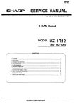
SHARP
SERVICE MANUAL
CODE: OOZMZIE14//-E
MODEL
MZ-1E14
r-----------------------CONTENTS----------------------~
1. Specification . . . . . . . . . . . . . . . . . . . . . . . . . . . . . . . . . . . . . . . . . . . . . . . . . . . . . . . .
'-1. General specification . . . . . . . . . . . . . . . . . . . . . . . . . . . . . . . . . . . . . . . . . . . . . . . .
1-2. Buffered signals . . . . . . . . . . . . . . . . . . . . . . . . . . . . . . . . . . . . . . . . . . . . . . . . . . .
2. Block diagram . . . . . . . . . • • • . . . . . . . . . . . . . . . . . . . . . . . . . . . . . . . . . . . . . . . . . . .
2·1. Block diagram . . . . . . . . . . . • . . . . . . . . . . . . . . . . . . . . . • . . . . . . . . . . . . . . . . . .
2·2. Description . . . . • . . . • . . . . . . . . . . . . . . . . . . . . . . . . . . . . . . . . . . . . . . . . . . . ..
3. Troubleshooting. . . . . . . . . . . . . . . . . . • . . . . . . . . . . . . . . • . . . . . . . . . . . . . . . . . . ..
3·1. Troubleshooting procedure. . . . . . . . . . . . . . . . . . . . . . . . . . . . . . . . . . • . . . . . . . ..
3-2. Problem caused by the 1 E14 . . . . . . . . . . . . . . . . . . . . . . . . . . . . . . . . . . . . . . . . . ..
4. Circuit diagram
1
2
2
2
2
......................"................................
6
5. Parts & signal layout . . • . . . . . . . . . . . . . . . . . . . . . . . . • . . . . . . . . . . . . . . . • . . . . . . .
6. Parts guide . . . . . . . . . • . . . . . . . . . . . . • . . . . . . . . . . . • . . . . . . . . . . . . . . . . . . . . . .
7
8
SHARP CORPORATION
---------
-
MZ-IEI4
1. SPECIFICATION
1·1. General specification
See the wiring diagram for detail of
bus line connector and the 510
Pin configuration
connector.
TTL level
I nput/output electrical characteristics
Signal level
shall conform to the le used.
ICs used:
SN74LSOO SN74LS02 SN74LS04
SN74LS10 SN74LS30 SN74LS74
SN74LS138 SN74LS541 2732(ROM)
Input/output
specification
Operating temperature
5°C'" 35°C
Storage temperature
-15°C ...... 600 e
Supply voltage
5V±5%
(external power supply not needed
when used in conjunction with the 1 F11,
MZ-700).
Physical dimensjons
1·2. Buffered signals
The following signals are buffered by the SN74LA541.
IORO, RESET, RD, CE, 51, SO, <p, Ml
2. BLOCK DIAGRAM
2· 1. Block diagram
CPU DO-D7~~----------------------------------__~~~~~~__~----------__~DO-D7
CPU CLKO
" !F!!
Ml
CYCLE
CE
io<--...,..-J->/OE
ROM 4KB
ROM READ
1 WAIT
CPU WAIT
DO~D7
M!
CPU Ml
AO-A15
All ~12A13!A14Jtu5
ROM ADDRESS
TO !F!!
DECODER
CPU MERQ
......._ _ _-!-_ _-''""
,
CPU RD
i--------.... cPU
t,-_~
~------""CPU
BUFFER
AO
DRIVER
AI1A2 AB A4 A5 AS A7
I-------~S!
MEMORY BANK
r-----------~SO
SELECTOR
CPU WR
RESET
CPU lORQ
~L_J----.CE
"~-;===±=~r
!!L===~J
r---r-i~~~~~::~~~~----~
I
I I \1
AO\AdA2\AB\A4 A5 A6A7
QD I/O SELECTOR
t
-1-
CLK(BUS~)
Mi
~------------.CPU RD
r-------------.RESET
r-------------iOcPU !ORQ
MZ:,.IE14
---
-------
3.
2-2. Description
1) ROM
TROUBLESHOOTING-.o,~
I
__' . " '
_~J~..'".-,,_.
--I
The MZ disk monitor routine program is contained in
1) Troubleshooting procedure.~j, :.: I~'.
, - , ; :,_~", _;::> • ;
the ROM. It locates on the MZ·700 VRAM. key'side
In the first place .it become!_necessary to fine! out on
bank, dominating the 2 KB addresses of $E800 through
Which' sidethetrouble',;s; lE14 or 1 FH. GeNhe pro$EFFF. Even though the 2732, ROM has a 4 KB capaperlyiul1~tidriin'illEj:4':and'lFll connected with the
city, only 2 KB are used actually.
u"nit one-Oat --if time to fin~- .OU~ ~hich conne~~i~~ j.S~~~,es
The MZ-700 monitor ROM reads the contents of $E800
'"thetrouble;-,',---, """":,'
to check if it is $00. If so, the control advances to
2} Describ~d ~:ej(i are' 'p:osslb'le bills_as which may occur
__ _ _ _:::-~$~E"?8~0~0,.!f~0_':r~e~xe"!c~u~t~io~n!o._;_::_:_=_:_;:;:_--------_ _~__ wtten_e,ttte<_.tbe.-1-E.1_4_<l"_tE.1_1_is;.i"_c'mnectfuri...'~'_'i,',_'_.,-.- '-'- : -.' .. -. -, ,:::-.. - .. - ,- :-.;', - -':' i
,,-_J, 11 '
2) Ml CYCLE ROM READ 1 WAIT
This block is used to insert a single wait during the M1
g;1.' problem,c8uses.byjhe_tEt4,_
.,
cycle (op code fetch) of the Z·80 CPU in executing the
--~1) ROM·starts - -- - - _ _ __ '
"
contents of the above ROM, as it uses the memory of
The message, '''MAKE' READV"OD,"MONITOR
relatively sl6w access while a faster memory is required
•. 9Z·503M~,·,'~ does appear Oh,the display'whorf power is
for the memory read in the Ml cycle.
'i~,';ed ~ri"';ithth'ediskloaded'in the drive unit.
3) ROM ADDRESS DECODER
(2) , No operation.can tak~ 'place (including program wild
;i-i'iJi:i' :;':1
This block enables data output of the ROM when the
run)."
VRAM side bank has been assigned at 4) and that the
CPU has executed the read operation to the address
3-2. P~oblem .caused by the 1 Fit'
$E800 through $EFFF.
(1) ,
driei~.6t startiC' ruri. '
4) MEMORY BANK SELECTOR
(2) Write does take" place;"
, "
Performs to select the
o Write protect error occurs at all times.
memory bank. Only
o The message "NOT READY ERROR" displayed.
when the MZ·700 has $DO 0 0
o The data written
th~-disk can nc)t be read.
V-RAM
chosen the VRAM side
(3)
Read
is
not
enabled.
-- - --- -- --bank, it makes bank
V-RAM
$EOOO
output enabled.
Troubleshooting procedure -1 E14_,!(]:,L1.LM.MJl:!L
- (-1) RQMdoes not start.,
, -$E800
~
,
therri"to;
on
$FOOO
j
MZdisk
ROM
,
'
i
i
NO
$FFFF
YES
5) MZ DISK I/O SELECTOR.'
.
The SIO of the IFll is emibled only wh~n the CPU
accesses the I/O address of ihe MZ disk.
'
The table below shows the relatiori among address •. Sl,
SO, and CE.
I/O port
C/E
S1
SO
$F.4
$F5
$F6
$F7
0
0
0
0
0
0
0
1
1
0
I
1
1
NO
The MZ-700 monitor is
"HMONITOR lZ-013A**".
SIO register
Channel A
8
Channel A
Channel 8
~'Channel
DATA
,DATA
:CWR
CWR
6) BUFFER DRIVER
Not ,o-nly ehhances signal driving capacity to the signal
sent to the IFll, bUTr"doted influences to the,CPU as
much as pos_sit'Ie:.
7) 1 F 11 interfacing signals
a. CPU CLOCK (BUS <P) ••••.•• MZ·700 CPU clock
(3.85 MHz).
b. CPUMl . . . . . . . . Ml signal from the MZ-700 CPU"
c. CPURD . . . . . . . . . . RD signal from the MZ·780.
d. CPUIORO ...••••. 10RO signal from the MZ·7~0.
e. RESET . . . . . . . . • . . . MZ-700 system reset signal.
f. CE . • . . . . . . . . . . . . 1 Fll SIO chip enable' signal.
g. Sl . . . . . . . . • 1 F 11 SIO control/data select signal.
h. SO .....••.• 1 Fll SIO channel A/B select signal.
Examine the LS245
and wait circuit.
",==:7.====,
Check'if the
"OE" of,the ROM
~ea after, #EBOO does not appear. Examine the p-eriphery
.
-- ,
of the LS30
'(bank address decoder).
can be r.ead With the
,
- M command.........
,
, _All areas after $,E~OO should b
YES
L.
"7E" when power is not on.
~
.
,
ROM is in t.rouble. ,Replace the ROM
, with; the new ()lie.
MZ-IEI4
(2) No operation can take place
Proceed to examine
the ROM (Step (111.
NO
Check if the
ROM starts.
(b) Write is not enabled.
(1) Write protect error occurs at all times.
Set the disk in
the drive.
YES
Check if the.
~
rite protect~ab
NO
Check if the
SID access is
successful.
of the disk is
broken.
Examine the LS541
and bus line.
NO
VES <Check if CTSA
NO
of the SIO is low::.:>""---,
YES
Replace with the d i s l f V E S
whose write protect
tab is not broken.
Failure on the
1F11 side,
Check if WRPR
of T-4 is low.
CheCk i~ ot~e~rNO
~
operation IS
permitted.
NO
VES
r-==-=-L,-C7=-.--,
Replace the LS14
with the new one.
-1 F11{a} The motor does not start to run.
Conduct test while the LOAD command is in execution.
~
<Check if DTRB
Check if the
cableisin
connection.
<
NO
NO
>:::e..-i
Put the cable
into connection.
VES
Y
Examine the write
protect switch of
the drive unit.
Check if MTON
of T-4 is low.
NO
(2) The message "NOT READY ERROR" displayed.
Set the disk in
the drive.
VES
circuit pattern.
Check if the
BUSY lamp is on.
NO
<Check if DCDA~
YES
~
ay"
Check if MDST
NO
of T-4 is low
. . . . . Check if CPU ..........
bus line is functioning
A motor failure.
properly./'
VES
CheCk
~
if #2 pin ......
of the Control Boardl>---i
IC6islow./
Examine the
IC11 and IC12.
Defect in the SIO.
Check if
the cable is in
connection.
~3-
NO
Put the cable
into connection.
,---,
----IMZ"'-lcE144------------
(3) Write is not enabled.
";j,
)"; :'i
"-.
Check jf
(c) Read is not enabled.
".: " ,;
, ': •.:" c
Set the disk in the MZ disk and conduct test while the
LOACLc9mJTl~J:1d is in execution.
·,;i·
::-i:::;'
NO
read is enabled. : ; , : ; ; : ' - - - - - - - - - - - ,
Check if the
YES
clock is on.
;:N",O,,-_ _,
...
P'rocee'd'id
traubleshoo1: the
~e~q t"u:nct1ion.
YES
<
Check if the
disk has b~!I]._
set proper,ly.
YES
Check if R DDT
inp:ut is on.
" i~
NO
')1':
1'1 I )
,\r!
NO
1
Check if RTS B
is turning on
and off.
"J:','l
~~heck if the
~Y5tal clo'ck is
r-I-:~.,.:-;~.l:"~":-d-,--, 'X~'<
6'~:"",:~;'
NO
_~~place the crystal
with the new one.
outp~,t ~s !-9wY~'>"---'
YES
Check if
<RXCA and RXDA
.......... mputs are on.
ExamiJiEi'the read
amplifier
cftgital"'CirC'uit.
or
NO
>"-_--,
YES
Failure in the 510.
Failure in the 510.
ES
Failure in' the LS04.
NO
Examine the periphery
ES
NO
J
of the LS393.
_Check if
r--'""""'C CL 01 'he LS74
is}ligH; .
. YES
r
_ _....!:!N~OCCheck if WRPR
, of Tl4' is on.
YES
';"
Examine·.the
write line_of
th~ M"Z "dis~ dri,ve.
-'4-
or
replace the- pad.
YES
'T
NO
"Adjust·off~track
NO
Y~S
Procedure after this need to
conduct test while writing.
Check if RTSA
Check a proper
"- -<waveform is seen NO
on the test point 1.
YES
- --
-
MZ-IEI4
* Procedure to examine the SIO bus line (with the MZ700,1 E14, 1 Fll in connection).
An example to test proper connection of the bus line up
to the 510.
Write the interrupt vector in the write register 2 of the
channel 8 and read it out of the read register 2.
**
01
02
03
04
05
06
07
08
09
10
11
12
13
14
15
16
17
18
19
20
21
22
23
24
0000
0000
0000
0000
0003
0006
0009
OOOB
0000
OOOF
0011
0013
0015
0016
0018
OOlA
001C
001E
0020
0021
0023
0026
0026
0026
Z80 ASSEMBLER 2Z-004C
(QSCK-O>
PAGE 01
QOC SIO CHECK PROGRAM
•
210001
11 AA55
01F702
E061
E069
E041
E051
E041
E078
BA
20E8
E041
E059
E041
E078
BB
2000
C304E8
•
START: LO
LO
LO
OUT
OUT
OUT
OUT
OUT
IN
CP
HL.0100H
OE.55AAH
BC.02F7H
(C) • H
(C)
(C)
(C)
(C)
•L
•B
.0
•B
A. (C)
o
JR
NZ.START
OUT
OUT
OUT
IN
CP
(C) • B
(C) • E
(C) • B
A. (C)
E
JP
NZ.START
E804H
JR
END
Immediately after the above test, the control goes into
the state of ready for monitor command, if the SIO data
have been read correctly, that is, the control jumps to
$OOAD. If there is any failure, the control goes to
execute indefinite program looping. In this case, there
may be a failure like open cable, buffer failure, or SIO
failure in the worst case.
-5-
?????
.-,.
---_~¥Z=lEl""4l__-----------
-------
-- - -
4. CIRCUIT DIAGRAM
, '"
"
,,-
r
J;
:
,.,-: ,
,
;:
,;
~
",D?,,_:
"'
~~
"'
,--;;;---c r "'
"'
,
,-"
1,1:
"
_ n.
,--,I, ';;'.
"
,
~lt: i"
:1" ,
' D'
"
A"
rMERQ
, ,'.
';
, ,
;C.
", "
5
",4
2 ;PIf i
,
~,ICIO
: 12dP~~
"n: oS:
"
,
6 le?
LSD-I
-J
;
, '".
,
LSD'I
"
~
,
,
,
M'
".
D'
~
,
L_t}3
D4
,"'-=-
D,
D,
Q!U
L'D6
eK
LS~O
D
LS14
'"r
" 'Q
r-'-'
--
,-
Q
4C 10 I ,
~
.,
'1
-J
~-
"
:.tt::
'
~
-,
_.
,
.r@y],
~b'
l;rg;~Cll '):C9 ' i
... '" "" - <>
00_0 0
0000
,e,
2732K
lA
"'''''''''''''''_'''' _o~12
««««<-«,<'
",J;'~""" ;,.:,1,1,:::~'"
~
.-_.
M<
,,-,
'
lOOpF
--
"
"
"'.
" "
,
LSCO
~
I~
~."
LS14
;c
,
a
EXWAIT
:,
,
17 16 [5 14 13 11 10
5e
K
5C' -" 11
;l . ..
[CIO
1
'-"
','
,
,
.'\:
i' j
+OV
;-,
['CS 56
. .
,
rAiii"""l-
,
•
••
, '" ,o
.e
I.SD2
,c.
"{S04
,,<
"'.
~
=,
'~3
'c.
'" , "
~
...
~w
,
'\VR
,e
[~
,
6 LS!38
LS02
"'
A
[ca
AO
,
M
L~1l4
10
LSIO
[ca
IC8 LS02
~~~a~ ~w
,e
"
, 4B~
MW
AO
AO
,e,
LSOO
~Lsa2
ac
"
,~
". "
"
A'
~
M
..
.,"
'.
"
"
"
",
,
•
,•
U
CNO
CND
OND
J::X-\VAlT
AO
~'
,
NC
OND
MERQ
" 1m
" '"
"
'" -.rr
"
..
'" "
~
,
Ne
..
"
AO
' AO
OND
AO
'A I'
A 0"
Busi"
D ,
D •
D •
D ,
D ,
D •
D'
D •
M
NC
""
Ne
, RESET
Hi'
GND
"
"
",
'"
,•
,
GND
GND
GNO
GNO
GND
GND
GND
GND
T-'
~
~
SO
"
"
"
,,,"
, AID
A'9"
'--
cooo
::J
"
"
,
" M'
" M'
M'
"" M.
A"
.,""
" ."
"
A
'" ."
Yr--l6
~
,lOHQ:.J
T-'
~p..L
CM
.p
.~
CONNECTOR-7
PARTS _SIDE SOLDER 5 [DE
,
G"
J
I
RD
I
,
"1~ " ,
,c. "". "
.~
,, , "p::-.
,"
,, ,, "
"
•"
, C
MI
~
" •'
~oo
I , '"
.
"
"
"
~
"
"
"AO
"
2~19
,n-
COM
~
.~
B~12'
"
r;;-;
CONNECTOR-G
PARST-SIDE SOLDER-S I DE
M
+OV
"
" ",
"
"
"
"
"
L"
r:w-
RES[n
1fT
D'
D'
U
D'
D.
D'
D'
DJ
D,
-;.]6-
....
..
~
GND
"'0
""
" 'TIiRil"
"
"
"co,
GND
GND
"D
"D
"D
GND
"D
GND
-
M Z-1EI4
5. PARTS & SIGNAL LAYOUT
-7-
,-,
----,M~1E_14___---
---"'\ ' J
6. PARTS GUIDE
ITl
EXTERIORS
NO.
PARTS CODE
I o C F 6 9 5001///
2 o C F 6 9 5000///
3 oC F 6 9 5021///
4 OCF69 5 0 2 6 / / /
5 o C F 6 9 0005///
6 o C-EJ; '1.=0 0
PRICE NEW
RANK MARK
AM
N
AH
N
AB
N
AB
N
AA
N
PART
DESCRIPTION
RANK
C
[/F Ca binet u er
C
[iF Cabinet lower
C
Insulator
C
Leg For Cabinet
C
Screw (M3X6
1
...-c-\-SGrew-fMJ..X-6
!
[2J ELECTRONIC PARTS
NO.
I
2
3
4
5
6
7
8
9
PARTS CODE
VHiSN74LSOO
VHiSN74LS02
I
I
I
I
I
VHiSN74LS04
VHiSN74LSIO
VHiSN74LS30
VHiSN74LS74AN
VHiSN74LSI38N
VHiSN74LS541N
VHi 2732//AC88
10 o C F 6 9 5 1 0 5 / / /
11 o C F 6 9 5 1 0 3 / / /
12 o C F 6 9 5 1 0 4 / / /
13 o C F 6 9 5 0 9 5 / / /
14 o C F 6 9 5 0 9 2 / / /
15 o C F 6 9 5 0 2 3 / / /
PRICE
RANK
AE
AE
AE
AE
AE
AG
AG
AP
BK
AF
AM
AT
AC
AC
AA
NEW
MARK
N
N
N
N
N
N
N
PART
RANK
B
B
B
B
B
B
B
B
B
B
C
C
C
C
C
DESCRIPTION
IC
IC
IC
IC
IC
IC
IC
IC
EP
Rom
re socket'
-
-
-
[IC4,IC9]
[lCB]
[lC6]
[lC3]
[lC7l
[ICID]
[lC2]
[IC5]
[lCI]
.'-'
[T6]
Connector
Connector
Capacitor
Capacitor
[T7]
[C3]
[CI-2 C4 9]
Screw
W PACKING,INST.BOOK,OTHER
NU
PARTS CODE
I RMEMRI028AC73
2 TiNSE1140ACZZ
3
TiNSE1215ACZZ
4
5
6
7
8
9
10
11
TiNSEI216ACZZ
TSELFI002ACZZ
SPAKAI467ACZZ
SPAKCI562ACZZ
SSAKAOOOISCZZ
SSAKAO 3 0 2CCZZ
SSAKB0002YDEO
QCNW 1I05ACZZ
PRICE NEW
RANK MARK
BF
N
BB
N
AL
N
AP
N
AA
AM
N
AT
N
AA
AA
AA,
AK
N
PART
RANK
E
D
D
-D
D
D
D
D
D
D
C
DESCRIPTION
Master Disk
Instruction book Disk basic) (Disk Basic
Instruction Book Installation
Instruction book COD Basic)
Label
Packing Cushion _
Packin Case
Pol Ba: Instruction Book
Polv Sag(I/F unit
Poly Bag(Media
Cable for CMT
-
6-+---1[.'?~
I
@
-....'-,g.-
\
~~
-
_ _~MZ=1_Eu~14",--_ _ _~_ _ _ _ _ _ _ _ _ _ _ _ _ _ _ _ _ _ _ _ _ _ _ _ _ _ _ _ _ _ _ _ _ _ _ _ _
SHARP
SHARP CORPORATION
Industri~_llnstruments Group
Reliability & Quality Control Department
Yamatokoriyama, Nara 639-11, Japan
1984 August Printed in Japan
®