1
OpenSPARC™ T1 Microarchitecture
Specification
Sun Microsystems, Inc.
www.sun.com
Part No. 819-6650-10
August 2006, Revision A
Submit comments about this document at: http://www.sun.com/hwdocs/feedback
Copyright © 2006 Sun Microsystems, Inc., 4150 Network Circle, Santa Clara, California 95054, U.S.A. All rights reserved.
Sun Microsystems, Inc. has intellectual property rights relating to technology embodied in the product that is described in this document. In
particular, and without limitation, these intellectual property rights may include one or more of the U.S. patents listed at
http://www.sun.com/patents and one or more additional patents or pending patent applications in the U.S. and in other countries.
U.S. Government Rights - Commercial software. Government users are subject to the Sun Microsystems, Inc. standard license agreement and
applicable provisions of the FAR and its supplements.
Use is subject to license terms.
This distribution may include materials developed by third parties.
Sun, Sun Microsystems, the Sun logo, Solaris, OpenSPARC T1 and UltraSPARC are trademarks or registered trademarks of Sun Microsystems,
Inc. in the U.S. and other countries.
All SPARC trademarks are used under license and are trademarks or registered trademarks of SPARC International, Inc. in the U.S. and other
countries. Products bearing SPARC trademarks are based upon architecture developed by Sun Microsystems, Inc.
UNIX is a registered trademark in the U.S. and other countries, exclusively licensed through X/Open Company, Ltd.
The Adobe logo is a registered trademark of Adobe Systems, Incorporated.
Products covered by and information contained in this service manual are controlled by U.S. Export Control laws and may be subject to the
export or import laws in other countries. Nuclear, missile, chemical biological weapons or nuclear maritime end uses or end users, whether
direct or indirect, are strictly prohibited. Export or reexport to countries subject to U.S. embargo or to entities identified on U.S. export exclusion
lists, including, but not limited to, the denied persons and specially designated nationals lists is strictly prohibited.
DOCUMENTATION IS PROVIDED "AS IS" AND ALL EXPRESS OR IMPLIED CONDITIONS, REPRESENTATIONS AND WARRANTIES,
INCLUDING ANY IMPLIED WARRANTY OF MERCHANTABILITY, FITNESS FOR A PARTICULAR PURPOSE OR NON-INFRINGEMENT,
ARE DISCLAIMED, EXCEPT TO THE EXTENT THAT SUCH DISCLAIMERS ARE HELD TO BE LEGALLY INVALID.
Copyright © 2006 Sun Microsystems, Inc., 4150 Network Circle, Santa Clara, California 95054, Etats-Unis. Tous droits réservés.
Sun Microsystems, Inc. détient les droits de propriété intellectuels relatifs à la technologie incorporée dans le produit qui est décrit dans ce
document. En particulier, et ce sans limitation, ces droits de propriété intellectuelle peuvent inclure un ou plus des brevets américains listés à
l’adresse http://www.sun.com/patents et un ou les brevets supplémentaires ou les applications de brevet en attente aux Etats - Unis et dans les
autres pays.
L’utilisation est soumise aux termes de la Licence.
Cette distribution peut comprendre des composants développés par des tierces parties.
Sun, Sun Microsystems, le logo Sun, Solaris, OpenSPARC T1 et UltraSPARC sont des marques de fabrique ou des marques déposées de Sun
Microsystems, Inc. aux Etats-Unis et dans d’autres pays.
Toutes les marques SPARC sont utilisées sous licence et sont des marques de fabrique ou des marques déposées de SPARC International, Inc.
aux Etats-Unis et dans d’autres pays. Les produits portant les marques SPARC sont basés sur une architecture développée par Sun
Microsystems, Inc.
UNIX est une marque déposée aux Etats-Unis et dans d’autres pays et licenciée exlusivement par X/Open Company, Ltd.
Le logo Adobe. est une marque déposée de Adobe Systems, Incorporated.
Les produits qui font l’objet de ce manuel d’entretien et les informations qu’il contient sont regis par la legislation americaine en matiere de
controle des exportations et peuvent etre soumis au droit d’autres pays dans le domaine des exportations et importations. Les utilisations
finales, ou utilisateurs finaux, pour des armes nucleaires, des missiles, des armes biologiques et chimiques ou du nucleaire maritime,
directement ou indirectement, sont strictement interdites. Les exportations ou reexportations vers des pays sous embargo des Etats-Unis, ou
vers des entites figurant sur les listes d’exclusion d’exportation americaines, y compris, mais de maniere non exclusive, la liste de personnes qui
font objet d’un ordre de ne pas participer, d’une facon directe ou indirecte, aux exportations des produits ou des services qui sont regi par la
legislation americaine en matiere de controle des exportations et la liste de ressortissants specifiquement designes, sont rigoureusement
interdites.
LA DOCUMENTATION EST FOURNIE "EN L’ETAT" ET TOUTES AUTRES CONDITIONS, DECLARATIONS ET GARANTIES EXPRESSES
OU TACITES SONT FORMELLEMENT EXCLUES, DANS LA MESURE AUTORISEE PAR LA LOI APPLICABLE, Y COMPRIS NOTAMMENT
TOUTE GARANTIE IMPLICITE RELATIVE A LA QUALITE MARCHANDE, A L’APTITUDE A UNE UTILISATION PARTICULIERE OU A
L’ABSENCE DE CONTREFACON.
Please
Recycle
Contents
Preface
1.
xix
OpenSPARC T1 Overview
1–1
1.1
Introducing the OpenSPARC T1 Processor
1.2
Functional Description
1.3
OpenSPARC T1 Components
1.3.1
SPARC Core
1–1
1–2
1–4
1–4
1.3.1.1
Instruction Fetch Unit
1.3.1.2
Execution Unit
1.3.1.3
Load/Store Unit
1.3.1.4
Floating-Point Frontend Unit
1.3.1.5
Trap Logic Unit
1.3.1.6
Stream Processing Unit
1.3.2
CPU-Cache Crossbar
1.3.3
Floating-Point Unit
1.3.4
L2-Cache
1.3.5
DRAM Controller
1.3.6
I/O Bridge
1.3.7
J-Bus Interface
1.3.8
Serial System Interface
1–6
1–6
1–6
1–7
1–7
1–8
1–8
1–9
1–10
1–11
1–11
1–11
1–12
iii
1.3.9
2.
SPARC Core
1–12
2–1
2.1
SPARC Core Overview and Terminology
2.2
SPARC Core I/O Signal List
2.3
Instruction Fetch Unit
2.4
iv
Electronic Fuse
2–2
2–5
2–6
2.3.1
SPARC Core Pipeline
2.3.2
Instruction Fetch
2.3.3
Instruction Registers and Program Counter Registers
2.3.4
Level 1 Instruction Cache
2.3.5
I-Cache Fill Path
2.3.6
Alternate Space Identifier Accesses, I-Cache Line Invalidations,
and Built-In Self-Test Accesses to the I-Cache 2–11
2.3.7
I-Cache Miss Path
2.3.8
Windowed Integer Register File
2.3.9
Instruction Table Lookaside Buffer
2.3.10
Thread Selection Policy
2.3.11
Thread States
2.3.12
Thread Scheduling
2.3.13
Rollback Mechanism
2.3.14
Instruction Decode
2.3.15
Instruction Fetch Unit Interrupt Handling
2.3.16
Error Checking and Logging
Load Store Unit
2–7
2–8
2–9
2–9
2–10
2–12
2–13
2–15
2–15
2–16
2–18
2–19
2–20
2–21
2–21
2.4.1
LSU Pipeline
2–22
2.4.2
Data Flow
2.4.3
Level 1 Data Cache (D-Cache)
2.4.4
Data Translation Lookaside Buffer
2.4.5
Store Buffer
2–22
2–25
OpenSPARC T1 Microarchitecture Specification • August 2006
2–23
2–24
2–20
2.4.6
Load Miss Queue
2–26
2.4.7
Processor to Crossbar Interface Arbiter
2.4.8
Data Fill Queue
2.4.9
ASI Queue and Bypass Queue
2.4.10
Alternate Space Identifier Handling in the Load Store Unit
2.4.11
Support for Atomic Instructions (CAS, SWAP, LDSTUB)
2.4.12
Support for MEMBAR Instructions
2.4.13
Core-to-Core Interrupt Support
2.4.14
Flush Instruction Support
2.4.15
Prefetch Instruction Support
2.4.16
Floating-Point BLK-LD and BLK-ST Instructions Support
2.4.17
Integer BLK-INIT Loads and Stores Support
2.4.18
STRM Load and STRM Store Instruction Support
2.4.19
Test Access Port Controller Accesses and Forward Packets
Support 2–31
2.4.20
SPARC Core Pipeline Flush Support
2.4.21
LSU Error Handling
2–27
2.5
Execution Unit
2.6
Floating-Point Frontend Unit
2.7
2–28
2–28
2–29
2–29
2–29
2–30
2–30
2–31
2–31
2–32
2–32
2–33
2–35
Functional Description of the FFU
2.6.2
Floating-Point Register File
2.6.3
FFU Control (FFU_CTL)
2.6.4
FFU Data-Path (FFU_DP)
2.6.5
FFU VIS (FFU_DP)
2.7.1
2.8
2–27
2.6.1
Multiplier Unit
2–26
2–35
2–36
2–36
2–37
2–37
2–37
Functional Description of the MUL
Stream Processing Unit
2–37
2–38
2.8.1
ASI Registers for the SPU
2–38
2.8.2
Data Flow of Modular Arithmetic Operations
2–40
Contents
v
2.9
2.10
2.8.3
Modular Arithmetic Memory (MA Memory)
2.8.4
Modular Arithmetic Operations
Memory Management Unit
2–41
2–43
2.9.1
The Role of MMU in Virtualization
2.9.2
Data Flow in MMU
2.9.3
Structure of Translation Lookaside Buffer
2.9.4
MMU ASI Operations
2.9.5
Specifics on TLB Write Access
2–48
2.9.6
Specifics on TLB Read Access
2–48
2.9.7
Translation Lookaside Buffer Demap
2.9.8
TLB Auto-Demap Specifics
2.9.9
TLB Entry Replacement Algorithm
2.9.10
TSB Pointer Construction
Trap Logic Unit
2–40
2–44
2–45
2–45
2–47
2–48
2–49
2–49
2–49
2–50
2.10.1
Architecture Registers in the Trap Logic Unit
2.10.2
Trap Types
2.10.3
Trap Flow
2.10.4
Trap Program Counter Construction
2.10.5
Interrupts
2.10.6
Interrupt Flow
2.10.7
Interrupt Behavior and Interrupt Masking
2.10.8
Privilege Levels and States of a Thread
2.10.9
Trap Modes Transition
2–52
2–53
2–55
2–57
2–57
2–58
2.10.10 Thread States Transition
2–61
2–61
2–62
2–63
2.10.11 Content Construction for Processor State Registers
2.10.12 Trap Stack
2–65
2.10.13 Trap (Tcc) Instructions
2–66
2.10.14 Trap Level 0 Trap for Hypervisor
vi
OpenSPARC T1 Microarchitecture Specification • August 2006
2–66
2–64
2.10.15 Performance Control Register and Performance Instrumentation
Counter 2–66
3.
CPU-Cache Crossbar
3.1
Functional Description
3–1
3.1.1
CPU-Cache Crossbar Overview
3–1
3.1.2
CCX Packet Delivery
3.1.3
Processor-Cache Crossbar Packet Delivery
3–3
3.1.4
Cache-Processor Crossbar Packet Delivery
3–4
3.1.5
CPX and PCX Packet Formats
3–2
3–5
3.2
CCX I/O List
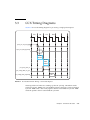
3.3
CCX Timing Diagrams
3.4
PCX Internal Blocks Functional Description
3.5
4.
3–1
3–13
3.4.1
PCX Overview
3.4.2
PCX Arbiter Data Flow
3.4.3
PCX Arbiter Control Flow
3.5.1
CPX Overview
3.5.2
CPX Arbiters
3–17
3–17
3–18
3–19
CPX Internal Blocks Functional Description
Level 2 Cache
4.1
3–9
3–20
3–20
3–20
4–1
L2-Cache Functional Description
4–1
4.1.1
L2-Cache Overview
4–1
4.1.2
L2-Cache Single Bank Functional Description
4.1.2.1
Arbiter
4–4
4.1.2.2
L2 Tag
4–4
4.1.2.3
L2 VUAD States
4–4
4.1.2.4
L2 Data (scdata)
4–5
4.1.2.5
Input Queue
4.1.2.6
Output Queue
4–2
4–5
4–6
Contents
vii
4.1.3
4.1.4
4.1.5
4.2
5.
Snoop Input Queue
4.1.2.8
Miss Buffer
4.1.2.9
Fill Buffer
4.1.2.10
Writeback Buffer
4.1.2.11
Remote DMA Write Buffer
4.1.2.12
L2-Cache Directory
L2-Cache Pipeline
4–6
4–7
4–8
4–8
4–8
4–9
L2-Cache Transaction Types
4.1.3.2
L2-Cache Pipeline Stages
L2-Cache Instruction Descriptions
4–9
4–10
4–12
4.1.4.1
Loads
4–12
4.1.4.2
Ifetch
4–12
4.1.4.3
Stores
4–13
4.1.4.4
Atomics
4.1.4.5
J-Bus Interface Instructions
4.1.4.6
Eviction
4.1.4.7
Fill
4.1.4.8
Other Instructions
4–13
4–14
4–16
4–16
4–16
L2-Cache Memory Coherency and Instruction Ordering
L2-Cache I/O LIST
4–18
5–1
Functional Description
5–1
5.1.1
IOB Interfaces
5–2
5.1.2
UCB Interface
5–4
5.1.3
4–6
4.1.3.1
Input/Output Bridge
5.1
viii
4.1.2.7
5.1.2.1
UCB Request and Acknowledge Packets
5.1.2.2
UCB Interrupt Packet
5.1.2.3
UCB Interface Packet Example
IOB Address Map
5–7
OpenSPARC T1 Microarchitecture Specification • August 2006
5–6
5–6
5–4
4–17
5.2
6.
5.1.4
IOB Block Diagram
5.1.5
IOB Transactions
5.1.6
IOB Interrupts
5.1.7
IOB Miscellaneous Functionality
5.1.8
IOB Errors
5.1.9
Debug Ports
6.1
6.2
7.
5–12
5–12
6–1
6–1
J-Bus Requests to the L2-Cache
6–3
6.1.1.1
Write Requests to the L2-Cache
6–3
6.1.1.2
Read Requests to the L2-Cache
6–4
6.1.1.3
Flow Control
6–4
6.1.2
I/O Buffer Requests to the J-Bus
6.1.3
J-Bus Interrupt Requests to the IOB
6.1.4
J-Bus Interface Details
6.1.5
Debug Port to the J-Bus
6.1.6
J-Bus Internal Arbitration
6.1.7
Error Handling in JBI
6.1.8
Performance Counters
I/O Signal list
Floating-Point Unit
7.1
5–11
5–11
Functional Description
6.1.1
5–9
5–10
I/O Bridge Signal List
J-Bus Interface
5–8
6–4
6–5
6–5
6–6
6–6
6–7
6–7
6–8
7–1
Functional Description
7–1
7.1.1
Floating-Point Instructions
7.1.2
FPU Input FIFO Queue
7.1.3
FPU Output Arbitration
7.1.4
Floating-Point Adder
7–4
7–5
7–6
7–6
Contents
ix
7.2
8.
Floating-Point Multiplier
7.1.6
Floating-Point Divider
7.1.7
FPU Power Management
7.1.8
Floating-Point State Register Exceptions and Traps
8.2
9.2
9.3
7–9
7.1.8.2
IEEE Exception List
I/O Signal list
7–12
7–13
7–15
8–1
Functional Description
8–1
8.1.1
Arbitration Priority
8.1.2
DRAM Controller State Diagrams
8.1.3
Programmable Features
8.1.4
Errors
8.1.5
Repeatability and Visibility
8.1.6
DDR-II Addressing
8.1.7
DDR-II Supported Features
I/O Signal List
8–3
8–5
8–6
8–6
8–7
8–8
8–9
9–1
Error Handling Overview
9–1
9.1.1
Error Reporting and Logging
9.1.2
Error Traps
9–2
SPARC Core Errors
9–3
9–2
9.2.1
SPARC Core Error Registers
9.2.2
SPARC Core Error Protection
9–4
9.2.3
SPARC Core Error Correction
9–4
L2-Cache Errors
9.3.1
x
7–8
Overflow and Underflow
Error Handling
9.1
7–7
7.1.8.1
DRAM Controller
8.1
9.
7.1.5
9–3
9–5
L2-Cache Error Registers
OpenSPARC T1 Microarchitecture Specification • August 2006
9–5
8–4
7–10
9.4
10.
9.3.2
L2-Cache Error Protection
9.3.3
L2-Cache Correctable Errors
9.3.4
L2-Cache Uncorrectable Errors
DRAM Errors
9–7
9–8
DRAM Error Registers
9.4.2
DRAM Error Protection
9.4.3
DRAM Correctable Errors
9.4.4
DRAM Uncorrectable and Addressing Errors
10.1.2
9–8
9–9
9–9
10–1
OpenSPARC T1 Processor Clocks
10–1
10.1.1.1
Phase-Locked Loop
10.1.1.2
Clock Dividers
10.1.1.3
Clock Domain Crossings
10.1.1.4
Clock Gating
10.1.1.5
Clock Stop
10.1.1.6
Clock Stretch
10–8
10.1.1.7
Clock n-Step
10–8
10.1.1.8
Clock Signal Distribution
10–3
10–4
10–5
10–7
10–7
OpenSPARC T1 Processor Resets
10–8
10–10
10.1.2.1
Power-On Reset (PWRON_RST_L)
10.1.2.2
J-Bus Reset (J_RST_L)
10.1.2.3
Reset Sequence
10.1.2.4
Debug Initialization
I/O Signal list
9–9
10–1
Functional Description
10.1.1
10.2
9–6
9.4.1
Clocks and Resets
10.1
9–6
10–10
10–11
10–11
10–15
10–15
Contents
xi
xii
OpenSPARC T1 Microarchitecture Specification • August 2006
Figures
FIGURE 1-1
OpenSPARC T1 Processor Block Diagram
1–3
FIGURE 1-2
SPARC Core Pipeline 1–5
FIGURE 1-3
CCX Block Diagram
FIGURE 2-1
SPARC Core Block Diagram 2–2
FIGURE 2-2
Physical Location of Functional Units on an OpenSPARC T1 SPARC Core
FIGURE 2-3
Virtualization of Software Layers 2–4
FIGURE 2-4
SPARC Core Pipeline and Support Structures 2–7
FIGURE 2-5
Frontend of the SPARC Core Pipeline
FIGURE 2-6
I-Cache Fill Path
FIGURE 2-7
I-Cache Miss Path 2–12
FIGURE 2-8
IARF and IWRF File Structure
FIGURE 2-9
Basic Transition of Non-Active States 2–16
FIGURE 2-10
Thread State Transition of an Active Thread 2–17
FIGURE 2-11
State Transition for a Thread in Speculative States
FIGURE 2-12
Rollback Mechanism Pipeline Graph 2–19
FIGURE 2-13
LSU Pipeline Graph 2–22
FIGURE 2-14
LSU Data Flow Concept 2–23
FIGURE 2-15
Execution Unit Diagram
FIGURE 2-16
Shifter Block Diagram 2–34
FIGURE 2-17
ALU Block Diagram
1–9
2–3
2–8
2–10
2–14
2–18
2–33
2–34
xiii
FIGURE 2-18
IDIV Block Diagram
FIGURE 2-19
Top-Level FFU Block Diagram 2–36
FIGURE 2-20
Multiplexor (MUL) Block Diagram 2–37
FIGURE 2-21
Layout of MA_ADDR Register Bit Fields
FIGURE 2-22
Data Flow of Modular Arithmetic Operations 2–40
FIGURE 2-23
State Transition Diagram Illustrating MA Operations
FIGURE 2-24
Multiply Function Result Generation Sequence Pipeline Diagram
FIGURE 2-25
MMU and TLBs Relationship 2–44
FIGURE 2-26
Virtualization Diagram
FIGURE 2-27
Translation Lookaside Buffer Structure
FIGURE 2-28
TLU Role With Respect to All Other Backlogs in a SPARC Core 2–51
FIGURE 2-29
Trap Flow Sequence 2–55
FIGURE 2-30
Trap Flow With Respect to the Hardware Blocks
FIGURE 2-31
Flow of Hardware and Vector Interrupts
FIGURE 2-32
Flow of Reset or Idle or Resume Interrupts 2–59
FIGURE 2-33
Flow of Software and Timer Interrupts 2–60
FIGURE 2-34
Trap Modes Transition
FIGURE 2-35
Thread State Transition 2–63
FIGURE 2-36
PCR and PIC Layout
FIGURE 3-1
CPU Cache-Crossbar (CCX) Interface
FIGURE 3-2
Processor Cache-Crossbar (PCX) Interface 3–2
FIGURE 3-3
Cache-Processor Crossbar (CPX) Interface 3–4
FIGURE 3-4
PCX Packet Transfer Timing – One Packet Request 3–13
FIGURE 3-5
PCX Packet Transfer Timing – Two-Packet Request
FIGURE 3-6
CPX Packet Transfer Timing Diagram – One Packet Request 3–15
FIGURE 3-7
CPX Packet Transfer Timing Diagram – Two Packet Request
FIGURE 3-8
PCX and CPX Internal Blocks
FIGURE 3-9
Data Flow in PCX Arbiter
FIGURE 3-10
Control Flow in PCX Arbiter 3–19
FIGURE 4-1
Flow Diagram and Interfaces for an L2-Cache Bank 4–3
xiv
2–35
2–38
2–41
2–43
2–44
2–46
2–56
2–58
2–62
2–67
3–2
3–14
3–17
3–18
OpenSPARC T1 Microarchitecture Specification • August 2006
3–16
FIGURE 5-1
IOB Interfaces
5–2
FIGURE 5-2
IOB UCB Interface to and From the Cluster
FIGURE 5-3
IOB Internal Block Diagram
FIGURE 6-1
JBI Functional Block Diagram
FIGURE 7-1
FPU Functional Block Diagram 7–2
FIGURE 8-1
DDR-II DRAM Controller Functional Block Diagram 8–2
FIGURE 8-2
DDR-II DRAM Controller Top-Level State Diagram
FIGURE 8-3
DIMM Scheduler State Diagram
FIGURE 10-1
Clock and Reset Functional Block Diagram 10–2
FIGURE 10-2
PLL Functional Block Diagram 10–3
FIGURE 10-3
Clock Divider Block Diagram 10–4
FIGURE 10-4
Sync Pulses Waveforms 10–6
FIGURE 10-5
Clock Signal Distribution 10–9
5–4
5–8
6–2
8–4
8–5
Figures
xv
xvi
OpenSPARC T1 Microarchitecture Specification • August 2006
Tables
TABLE 2-1
SPARC Core Terminology 2–4
TABLE 2-2
SPARC Core I/O Signal List
TABLE 2-3
Modular Arithmetic Operations
TABLE 2-4
Error Handling Behavior
TABLE 2-5
Supported OpenSPARC T1 Trap Types
TABLE 2-6
Privilege Levels and Thread States 2–61
TABLE 3-1
CPX Packet Format – Part 1 3–5
TABLE 3-2
CPX Packet Format – Part 2 3–6
TABLE 3-3
PCX Packet Format – Part 1 3–7
TABLE 3-4
PCX Packet Format – Part 2 3–8
TABLE 3-5
CCX I/O Signal List
TABLE 4-1
SCDATA I/O Signal List 4–18
TABLE 4-2
SCBUF I/O Signal List
TABLE 4-3
SCTAG I/O Signal List 4–21
TABLE 5-1
UCB interfaces to Clusters
TABLE 5-2
UCB Request/Acknowledge Packet format
TABLE 5-3
UCB Request/ACK Packet Types
TABLE 5-4
UCB Data Size
TABLE 5-5
UCB Interrupt Packet Format
TABLE 5-6
UCB Interrupt Packet Types 5–6
2–5
2–39
2–42
2–54
3–9
4–19
5–3
5–4
5–5
5–5
5–6
xvii
TABLE 5-7
UCB No Payload Over an 8-Bit Interface Without Stalls 5–6
TABLE 5-8
UCB No Payload Over an 8-Bit Interface With Stalls 5–7
TABLE 5-9
IOB Address Map
TABLE 5-10
I/O Bridge I/O Signal List 5–12
TABLE 6-1
JBI I/O Signal List 6–8
TABLE 7-1
OpenSPARC T1 FPU Feature Summary
TABLE 7-2
SPARC V9 Single and Double Precision FPop Instruction Set
TABLE 7-3
FPA Datapath Stages
TABLE 7-4
FPM Datapath Stages 7–8
TABLE 7-5
FPD Datapath Stages 7–9
TABLE 7-6
IEEE Exception Cases
TABLE 7-7
FPU I/O Signal List
TABLE 8-1
DDR-II Addressing 8–7
TABLE 8-2
Physical Address to DIMM Address Decoding
TABLE 8-3
DDR-II Commands Used by OpenSPARC T1 Processor
TABLE 8-4
DRAM Controller I/O Signal List 8–9
TABLE 9-1
Error Protection for SPARC Memories 9–4
TABLE 9-2
Error Protection for L2-Cache Memories 9–6
TABLE 10-1
Clock Domain Dividers
TABLE 10-2
CTU I/O Signal List 10–15
xviii
5–7
7–3
7–7
7–13
7–15
10–5
OpenSPARC T1 Microarchitecture Specification • August 2006
8–7
8–8
7–4
Preface
This OpenSPARC T1 Microarchitecture Specification includes detailed functional
descriptions of the core OpenSPARC™ T1 processor components. This manual also
provides the I/O signal list for each component. This processor is the first chip
multiprocessor that fully implements the Sun™ Throughput Computing initiative.
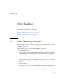
How This Document Is Organized
Chapter 1 introduces the processor and provides a brief overview of each processor
component.
Chapter 2 provides a detailed description of the functional units of a SPARC® Core.
Chapter 3 describes the CPU-cache crossbar (CCX) unit and includes detailed CCX
block and timing diagrams.
Chapter 4 provides a functional description of the L2-cache and describes the
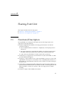
L2-cache pipeline and instructions.
Chapter 5 describes the processor’s input/output bridge (IOB).
Chapter 6 gives a functional description of the J-Bus interface (JBI) block.
Chapter 7 provides a functional description of the floating-point unit (FPU).
Chapter 8 describes the dynamic random access memory (DRAM) controller.
Chapter 9 provides a detailed overview of the processor’s error handling
mechanisms.
Chapter 10 gives a functional description of the processor’s clock and test unit
(CTU).
xix
Using UNIX Commands
This document might not contain information about basic UNIX® commands and
procedures such as shutting down the system, booting the system, and configuring
devices. Refer to the following for this information:
■
Software documentation that you received with your system
■
Solaris™ Operating System documentation, which is at:
http://docs.sun.com
Shell Prompts
Shell
Prompt
C shell
machine-name%
C shell superuser
machine-name#
Bourne shell and Korn shell
$
Bourne shell and Korn shell superuser
#
Typographic Conventions
Typeface1
Meaning
Examples
AaBbCc123
The names of commands, files,
and directories; on-screen
computer output
Edit your.login file.
Use ls -a to list all files.
% You have mail.
AaBbCc123
What you type, when contrasted
with on-screen computer output
% su
Password:
AaBbCc123
Book titles, new words or terms,
words to be emphasized.
Replace command-line variables
with real names or values.
Read Chapter 6 in the User’s Guide.
These are called class options.
You must be superuser to do this.
To delete a file, type rm filename.
1 The settings on your browser might differ from these settings.
xx
OpenSPARC T1 Microarchitecture Specification • August 2006
Related Documentation
The documents listed as online or download are available at:
http://www.opensparc.net/
Application
Title
Part Number
Format
Location
OpenSPARC T1 instruction set
UltraSPARC® Architecture 2005
Specification
950-4895
PDF
Online
OpenSPARC T1 processor’s internal
registers
UltraSPARC T1 Supplement to the
UltraSPARC Architecture 2005
819-3404
PDF
Online
OpenSPARC T1 megacells
OpenSPARC T1 Processor Megacell
Specification
819-5016
PDF
Download
OpenSPARC T1 signal pin list
OpenSPARC T1 Processor Datasheet
819-5015
PDF
Download
OpenSPARC T1 microarchitecture
OpenSPARC T1 Microarchitecture
Specification
819-6650
PDF
Download
OpenSPARC T1 processor
J-Bus and SSI interfaces
OpenSPARC T1 Processor External
Interface Specification
819-5014
PDF
Download
Documentation, Support, and Training
Sun Function
URL
OpenSPARC T1
http://www.opensparc.net/
Documentation
http://www.sun.com/documentation/
Support
http://www.sun.com/support/
Training
http://www.sun.com/training/
Preface
xxi
Third-Party Web Sites
Sun is not responsible for the availability of third-party web sites mentioned in this
document. Sun does not endorse and is not responsible or liable for any content,
advertising, products, or other materials that are available on or through such sites
or resources. Sun will not be responsible or liable for any actual or alleged damage
or loss caused by or in connection with the use of or reliance on any such content,
goods, or services that are available on or through such sites or resources.
xxii OpenSPARC T1 Microarchitecture Specification • August 2006
CHAPTER
1
OpenSPARC T1 Overview
This chapter contains the following topics:
■
■
■
1.1
Section 1.1, “Introducing the OpenSPARC T1 Processor” on page 1-1
Section 1.2, “Functional Description” on page 1-2
Section 1.3, “OpenSPARC T1 Components” on page 1-4
Introducing the OpenSPARC T1
Processor
The OpenSPARC T1 processor is the first chip multiprocessor that fully implements
the Sun Throughput Computing Initiative. The OpenSPARC T1 processor is a highly
integrated processor that implements the 64-bit SPARC V9 architecture. This
processor targets commercial applications such as application servers and database
servers.
The OpenSPARC T1 processor contains eight SPARC® processor cores, which each
have full hardware support for four threads. Each SPARC core has an instruction
cache, a data cache, and a fully associative instruction and data translation lookaside
buffers (TLB). The eight SPARC cores are connected through a crossbar to an on-chip
unified level 2 cache (L2-cache).
The four on-chip dynamic random access memory (DRAM) controllers directly
interface to the double data rate-synchronous DRAM (DDR2 SDRAM). Additionally,
there is an on-chip J-Bus controller that provides an interconnect between the
OpenSPARC T1 processor and the I/O subsystem.
1-1
1.2
Functional Description
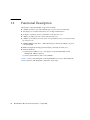
The features of the OpenSPARC T1 processor include:
■
8 SPARC V9 CPU cores, with 4 threads per core, for a total of 32 threads
■
132 Gbytes/sec crossbar interconnect for on-chip communication
■
16 Kbytes of primary (Level 1) instruction cache per CPU core
■
8 Kbytes of primary (Level 1) data cache per CPU core
■
3 Mbytes of secondary (Level 2) cache – 4 way banked, 12 way associative shared
by all CPU cores
■
4 DDR-II DRAM controllers – 144-bit interface per channel, 25 GBytes/sec peak
total bandwidth
■
IEEE 754 compliant floating-point unit (FPU), shared by all CPU cores
■
External interfaces:
■
J-Bus interface (JBI) for I/O – 2.56 Gbytes/sec peak bandwidth, 128-bit
multiplexed address/data bus
■
Serial system interface (SSI) for boot PROM
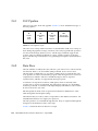
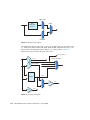
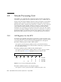
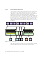
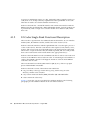
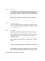
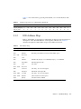
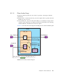
FIGURE 1-1 shows a block diagram of the OpenSPARC T1 processor illustrating the
various interfaces and integrated components of the chip.
1-2
OpenSPARC T1 Microarchitecture Specification • August 2006
OpenSPARC T1
FIGURE 1-1
OpenSPARC T1 Processor Block Diagram
Chapter 1
OpenSPARC T1 Overview
1-3
1.3
OpenSPARC T1 Components
This section provides further details about the OpenSPARC T1 components.
1.3.1
SPARC Core
Each SPARC core has hardware support for four threads. This support consists of a
full register file (with eight register windows) per thread, with most of the address
space identifiers (ASI), ancillary state registers (ASR), and privileged registers
replicated per thread. The four threads share the instruction, the data caches, and the
TLBs. Each instruction cache is 16 Kbytes with a 32-byte line size. The data caches
are write through, 8 Kbytes, and have a 16-byte line size. The TLBs include an
autodemap feature which enables the multiple threads to update the TLB without
locking.
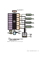
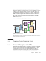
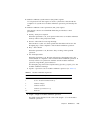
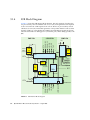
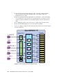
Each SPARC core has single issue, six stage pipeline. These six stages are:
1. Fetch
2. Thread Selection
3. Decode
4. Execute
5. Memory
6. Write Back
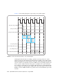
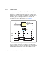
FIGURE 1-2 shows the SPARC core pipeline used in the OpenSPARC T1 Processor.
1-4
OpenSPARC T1 Microarchitecture Specification • August 2006
Fetch
Thrd Sel
Decode
Execute
Memory
Regfile
x4
ICache
Itlb
Inst
buf x 4
Thrd
Sel
Mux
Thread selects
Thrd
Sel
Mux
FIGURE 1-2
Decode
Thread
select
logic
WB
Crypto
Coprocessor
Alu
Mul
Shft
Div
DCache
Dtlb
Stbuf x 4
Crossbar
Interface
Instruction type
Misses
Traps and interrupts
Resource conflicts
PC logic
x4
SPARC Core Pipeline
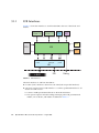
Each SPARC core has the following units:
1. Instruction fetch unit (IFU) includes the following pipeline stages – fetch, thread
selection, and decode. The IFU also includes an instruction cache complex.
2. Execution unit (EXU) includes the execute stage of the pipeline.
3. Load/store unit (LSU) includes memory and writeback stages, and a data cache
complex.
4. Trap logic unit (TLU) includes trap logic and trap program counters.
5. Stream processing unit (SPU) is used for modular arithmetic functions for crypto.
6. Memory management unit (MMU).
7. Floating-point frontend unit (FFU) interfaces to the FPU.
Chapter 1
OpenSPARC T1 Overview
1-5
1.3.1.1
Instruction Fetch Unit
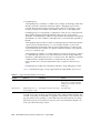
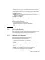
The thread selection policy is as follows – a switch between the available threads
every cycle giving priority to the least recently executed thread. The threads become
unavailable due to the long latency operations like loads, branch, MUL, and DIV, as
well as to the pipeline stalls like cache misses, traps, and resource conflicts. The
loads are speculated as cache hits, and the thread is switched-in with lower priority.
Instruction cache complex has a 16-Kbyte data, 4-way, 32-byte line size with a single
ported instruction tag. It also has dual ported (1R/1W) valid bit array to hold cache
line state of valid/invalid. Invalidates access the V-bit array, not the instruction tag.
A pseudo-random replacement algorithm is used to replace the cache line.
There is a fully associative instruction TLB with 64 entries. The buffer supports the
following page sizes: 8 Kbytes, 64 Kbytes, 4 Mbytes, and 256 Mbytes. The TLB uses
a pseudo least recently used (LRU) algorithm for replacement. Multiple hits in the
TLB are prevented by doing an autodemap on a fill.
Two instructions are fetched each cycle, though only one instruction is issued per
clock, which reduces the instruction cache activity and allows for an opportunistic
line fill. There is only one outstanding miss per thread, and only four per core.
Duplicate misses do not issue requests to the L2-cache.
The integer register file (IRF) of the SPARC core has 5 Kbytes with 3 read/2 write/1
transport ports. There are 640 64-bit registers with error correction code (ECC). Only
32 registers from the current window are visible to the thread. Window changing in
background occurs under the thread switch. Other threads continue to access the IRF
(the IRF provides a single-cycle read/write access).
1.3.1.2
Execution Unit
The execution unit (EXU) has a single arithmetic logic unit (ALU) and shifter. The
ALU is reused for branch address and virtual address calculation. The integer
multiplier has a 5 clock latency, and a throughput of half-per-cycle for area saving.
One integer multiplication is allowed outstanding per core. The integer multiplier is
shared between the core pipe (EXU) and the modular arithmetic (SPU) unit on a
round-robin basis. There is a simple non-restoring divider, which allows for one
divide outstanding per SPARC core. Thread issuing a MUL/DIV will be rolled back
and switched out if another thread is occupying the MUL/DIV units.
1.3.1.3
Load/Store Unit
The data cache complex has an 8-Kbyte data, 4-way, 16-byte line size. It also has
single ported data tag. There is a dual-ported (1R/1W) valid bit array to hold cache
line state of valid or invalid. Invalidates access the V-bit array but not the data tag. A
1-6
OpenSPARC T1 Microarchitecture Specification • August 2006
pseudo-random replacement algorithm is used to replace the data cache line. The
loads are allocating, and the stores are non-allocating. The data TLB operates
similarly to the instruction TLB.
The load/store unit (LSU) has an 8 entry store buffer per thread, which is unified
into a single 32 entry array, with RAW bypassing. Only a single load per thread
outstanding is allowed. Duplicate requests for the same line are not sent to the L2cache. The LSU has interface logic to interface to the CPU-cache crossbar (CCX). This
interface performs the following operations:
■
Prioritizes the requests to the crossbar for floating-point operation (Fpops),
streaming operations, I$ and D$ misses, stores and interrupts, and so on.
■
Request priority: imiss>ldmiss>stores,{fpu,stream,interrupt}.
■
Assembles packets for the processor-cache crossbar (PCX).
The LSU handles returns from the CPX crossbar and maintains the order for cache
updates and invalidates.
1.3.1.4
Floating-Point Frontend Unit
The floating-point frontend unit (FFU) decodes floating-point instructions and it also
includes the floating-point register file (FRF). Some of the floating-point instructions
like move, absolute value, and negate are implemented in the FFU, while the others
are implemented in the FPU. The following steps are taken when the FFU detects a
floating-point operation (Fpop):
1.3.1.5
■
The thread switches out.
■
The Fpop is further decoded and the FRF is read.
■
Fpops with operands are packetized and shipped over the crossbar to the FPU.
■
The computation is done in the FPU and the results are returned by way of the
crossbar.
■
Writeback completed to the FRF and the thread restarts.
Trap Logic Unit
The trap logic unit (TLU) has support for six trap levels. Traps cause pipeline flush
and thread switch until trap program counter (PC) becomes available. The TLU also
has support for up to 64 pending interrupts per thread.
Chapter 1
OpenSPARC T1 Overview
1-7
1.3.1.6
Stream Processing Unit
The stream processing unit (SPU) includes a modular arithmetic unit (MAU) for
crypto (one per core), and it supports asymmetric crypto (public key RSA) for up to
a 2048-byte size key. It shares an integer multiplier for modular arithmetic
operations. MAU can be used by one thread at a time. The MAU operation is set up
by the store to control register, and the thread returns to normal processing. The
MAU unit initiates streaming load/store operations to the L2-cache through the
crossbar, and compute operations to the multiplier. Completion of the MAU can be
checked by polling or issuing an interrupt.
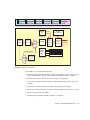
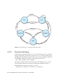
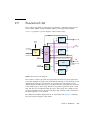
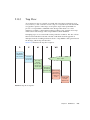
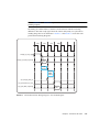
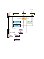
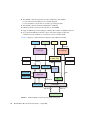
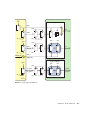
1.3.2
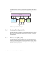
CPU-Cache Crossbar
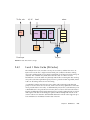
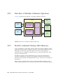
The eight SPARC cores, the four L2-cache banks, the I/O Bridge, and the FPU all
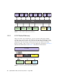
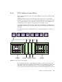
interface with the crossbar. FIGURE 1-3 displays the crossbar block diagram. The CPUcache crossbar (CCX) features include:
1-8
■
Each requester queues up to two packets per destination.
■
Three stage pipeline – request, arbitrate, and transmit.
■
Centralized arbitration with oldest requester getting priority.
■
Core-to-cache bus optimized for address plus doubleword store.
■
Cache-to-core bus optimized for 16-byte line fill. 32-byte I$ line fill delivered in
two back-to-back clocks.
OpenSPARC T1 Microarchitecture Specification • August 2006
Core 0
Core 1
Core 7
Core to L2 Cache, Shared FPU/CRI
C1
C7
FPU/CRI
Bank 0
Bank 1
C0
Core 7
Core 1
Core o
L2 Cache, FPU, CRI to Core
Bank 0
L2 Bank 0
FIGURE 1-3
1.3.3
L2 Bank 3
FPU
CRI
FPU
CRI
CCX Block Diagram
Floating-Point Unit
A single floating-point unit (FPU) is shared by all eight SPARC cores. The shared
floating-point unit is sufficient for most commercial applications in which typically
less than one percent of the instructions are floating-point operations.
Chapter 1
OpenSPARC T1 Overview
1-9
1.3.4
L2-Cache
The L2-cache is banked four ways, with the bank selection based on the physical
address bits 7:6. The cache is 3-Mbyte, 12-way set-associative with pseudo-least
recently used (LRU) replacement (the replacement is based on a used bit scheme).
The line size is 64 bytes. Unloaded access time is 23 cycles for an L1 data cache miss
and 22 cycles for an L1 instruction cache miss.
L2-cache has a 64-byte line size, with 64 bytes interleaved between banks. Pipeline
latency in the L2-cache is 8 clocks for a load, 9 clocks for an I-miss, with the critical
chunk returned first. 16 outstanding misses per bank are supported for a 64 total
misses. Coherence is maintained by shadowing the L1 tags in an L2-cache directory
structure (the L2-cache is a point of global visibility). DMA from the I/O is serialized
with respect to the traffic from the cores in the L2-cache.
The L2-cache directory shadows the L1 tags. The L1 set index and the L2-cache bank
interleaving is such that one forth of the L1 entries come from an L2-cache bank. On
an L1 miss, the L1 replacement way and set index identifies the physical location of
the tag which will be updated by the miss address. On a store, the directory will be
cammed. The directory entries are collated by set, so only 64 entries need to be
cammed. This scheme is quite power efficient. Invalidates are a pointer to the
physical location in the L1-cache, eliminating the need for a tag lookup in the L1cache.
Coherency and ordering in the L2-cache are described as:
■
Loads update directory and fill the L1-cache on return
■
Stores are non-allocating in the L1-cache
■
There are two flavors of stores: total store order (TSO) and read memory order
(RMO).
Only one outstanding TSO store to the L2-cache per thread is permitted in
order to preserve the store ordering. There is no such limitation on RMO
stores.
■
1-10
■
No tag check is done at a store buffer insert
■
Stores check directory and determines an L1-cache hit
■
Directory sends store acknowledgements or invalidates to the SPARC core
■
Store updates happens to D$ on a store acknowledge
Crossbar orders the responses across cache banks.
OpenSPARC T1 Microarchitecture Specification • August 2006
1.3.5
DRAM Controller
The OpenSPARC T1 processor DRAM controller is banked four ways, with each L2
bank interacting with exactly one DRAM controller bank (a two-bank option is
available for cost-constrained minimal memory configurations). The DRAM
controller is interleaved based on physical address bits 7:6, so each DRAM controller
bank must have identical dual in-line memory modules (DIMM) installed and
enabled.
The OpenSPARC T1 processor uses DDR2 DIMMs and can support one or two ranks
of stacked or unstacked DIMMs. Each DRAM bank/port is two-DIMMs wide (128bit + 16-bit ECC). All installed DIMMs must be identical, and the same number of
DIMMs (that is, ranks) must be installed on each DRAM controller port. The DRAM
controller frequency is an exact ratio of the core frequency, where the core frequency
must be at least three times the DRAM controller frequency. The double data rate
(DDR) data buses transfer data at twice the frequency of the DRAM controller
frequency.
The OpenSPARC T1 processor can support memory sizes of up to 128 Gbytes with a
25 Gbytes/sec peak bandwidth limit. Memory access is scheduled across 8 reads
plus 8 writes, and the processor can be programmed into a two-channel mode for a
reduced configuration. Each DRAM channel has 128 bits of data and 16 bytes of ECC
interface, with chipkill support, nibble error correction, and byte error detection.
1.3.6
I/O Bridge
The I/O bridge (IOB) performs an address decode on I/O-addressable transactions
and directs them to the appropriate internal block or to the appropriate external
interface (J-Bus or the serial system interface). Additionally, the IOB maintains the
register status for external interrupts.
1.3.7
J-Bus Interface
The J-Bus interface (JBI) is the interconnect between the OpenSPARC T1 processor
and the I/O subsystem. The J-Bus is a 200 MHz, 128-bit wide, multiplexed address
or data bus, used predominantly for direct memory access (DMA) traffic, plus the
programmable input/output (PIO) traffic used to control it.
The J-Bus interface is the functional block that interfaces to the J-Bus, receiving and
responding to DMA requests, routing them to the appropriate L2 banks, and also
issuing PIO transactions on behalf of the processor threads and forwarding
responses back.
Chapter 1
OpenSPARC T1 Overview
1-11
1.3.8
Serial System Interface
The OpenSPARC T1 processor has a 50 Mbyte/sec serial system interface (SSI) that
connects to an external application-specific integrated circuit (ASIC), which in turn
interfaces to the boot read-only memory (ROM). In addition, the SSI supports PIO
accesses across the SSI, thus supporting optional control status registers (CSR) or
other interfaces within the ASIC.
1.3.9
Electronic Fuse
The electronic fuse (e-Fuse) block contains configuration information that is
electronically burned-in as part of manufacturing, including part serial number and
core available information.
1-12
OpenSPARC T1 Microarchitecture Specification • August 2006
CHAPTER
2
SPARC Core
An OpenSPARC T1 processor contains eight SPARC cores, and each SPARC core has
several function units. These SPARC core units are described in the following
sections:
■
Section 2.1, “SPARC Core Overview and Terminology” on page 2-2
■
Section 2.2, “SPARC Core I/O Signal List” on page 2-5
■
Section 2.3, “Instruction Fetch Unit” on page 2-6
■
Section 2.4, “Load Store Unit” on page 2-21
■
Section 2.5, “Execution Unit” on page 2-33
■
Section 2.6, “Floating-Point Frontend Unit” on page 2-35
■
Section 2.7, “Multiplier Unit” on page 2-37
■
Section 2.8, “Stream Processing Unit” on page 2-38
■
Section 2.9, “Memory Management Unit” on page 2-43
■
Section 2.10, “Trap Logic Unit” on page 2-50
2-1
2.1
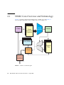
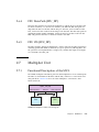
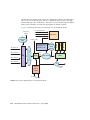
SPARC Core Overview and Terminology
FIGURE 2-1 presents a high-level block diagram of a SPARC core, and FIGURE 2-2
shows the general physical location of these units on an example core.
I-Cache
Strand
Instruction
Registers
Strand
Scheduler
Decode
ALU
Register
Files
Store Buffers
D-Cache
External
Interface
FIGURE 2-1
2-2
SPARC Core Block Diagram
OpenSPARC T1 Microarchitecture Specification • August 2006
MUL
EXU
IFU
MMU
LSU
Trap
FIGURE 2-2
0
2
4
6
1
3
5
7
Physical Location of Functional Units on an OpenSPARC T1 SPARC Core
Chapter 2
SPARC Core
2-3
TABLE 2-1 defines acronyms and terms that are used throughout this chapter.
SPARC Core Terminology
TABLE 2-1
Term
Description
Thread
A thread is a hardware strand (thread and strand will be used
interchangeably in this chapter). Each thread, or strand, enjoys a
unique set of resources in support of its execution while multiple
threads, or strands, within the same SPARC core will share a set of
common resources in support of their execution.
The per-thread resources include registers, a portion of I-fetch datapath, store buffer, and miss buffer. The shared resources include the
pipeline registers and data-path, caches, translation lookaside
buffers (TLB), and execution unit of the SPARC Core pipeline.
ST
Single threaded.
MT
Multi-threaded.
Hypervisor (HV)
The hypervisor is the layer of system software that interfaces with
the hardware.
Supervisor (SV)
The supervisor is the layer of system software such as operation
system (OS) that executes with privilege.
Long latency
instruction (LLI)
LLI represents an instruction that would take more than one SPARC
core clock cycle to make its results visible to the next instruction.
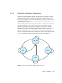
FIGURE 2-3 shows the view from virtualization, which illustrates the relative
privileges of the various software layers.
Applications
OS instance 1
OS instance 2
Hypervisor
OpenSPARC T1
FIGURE 2-3
2-4
Virtualization of Software Layers
OpenSPARC T1 Microarchitecture Specification • August 2006
2.2
SPARC Core I/O Signal List
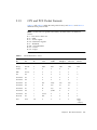
TABLE 2-2 lists and describes the SPARC Core I/O signals.
TABLE 2-2
SPARC Core I/O Signal List
Signal Name
I/O
Source/
Destination
Description
pcx_spc_grant_px[4:0]
In
CCX:PCX
PCX to processor grant info
cpx_spc_data_rdy_cx2
In
CCX:CPX
CPX data in-flight to SPARC
cpx_spc_data_cx2[144:0]
In
CCX:CPX
CPX to SPARC data packet
const_cpuid[3:0]
In
Hard wired
CPU ID
const_maskid[7:0]
In
CTU
Mask ID
ctu_tck
In
CTU
To IFU of sparc_ifu.v
ctu_sscan_se
In
CTU
To IFU of sparc_ifu.v
ctu_sscan_snap
In
CTU
To IFU of sparc_ifu.v
ctu_sscan_tid[3:0]
In
CTU
To IFU of sparc_ifu.v
ctu_tst_mbist_enable
In
CTU
To test_stub of test_stub_bist.v
efc_spc_fuse_clk1
In
EFC
efc_spc_fuse_clk2
In
EFC
efc_spc_ifuse_ashift
In
EFC
efc_spc_ifuse_dshift
In
EFC
efc_spc_ifuse_data
In
EFC
efc_spc_dfuse_ashift
In
EFC
efc_spc_dfuse_dshift
In
EFC
efc_spc_dfuse_data
In
EFC
ctu_tst_macrotest
In
CTU
To test_stub of test_stub_bist.v
ctu_tst_scan_disable
In
CTU
To test_stub of test_stub_bist.v
ctu_tst_short_chain
In
CTU
To test_stub of test_stub_bist.v
global_shift_enable
In
CTU
To test_stub of test_stub_two_bist.v
ctu_tst_scanmode
In
CTU
To test_stub of test_stub_two_bist.v
spc_scanin0
In
DFT
Scan in
spc_scanin1
In
DFT
Scan in
Chapter 2
SPARC Core
2-5
TABLE 2-2
SPARC Core I/O Signal List (Continued)
Signal Name
I/O
Source/
Destination
Description
cluster_cken
In
CTU
To spc_hdr of cluster_header.v
gclk
In
CTU
To spc_hdr of cluster_header.v
cmp_grst_l
In
CTU
Synchronous reset
cmp_arst_l
In
CTU
Asynchronous reset
ctu_tst_pre_grst_l
In
CTU
To test_stub of test_stub_bist.v
adbginit_l
In
CTU
Asynchronous reset
gdbginit_l
In
CTU
Synchronous reset
spc_pcx_req_pq[4:0]
Out
CCX:PCX
processor to pcx request
spc_pcx_atom_pq
Out
CCX:PCX
processor to pcx atomic request
spc_pcx_data_pa[123:0]
Out
CCX:PCX
processor to pcx packet
spc_sscan_so
Out
DFT
Shadow scan out
spc_scanout0
Out
DFT
Scan out
spc_scanout1
Out
DFT
Scan out
tst_ctu_mbist_done
Out
CTU
MBIST done
tst_ctu_mbist_fail
Out
CTU
MBIST fail
spc_efc_ifuse_data
Out
EFC
From IFU of sparc_ifu.v
spc_efc_dfuse_data
Out
EFC
From IFU of sparc_ifu.v
2.3
Instruction Fetch Unit
The instruction fetch unit (IFU) is responsible for maintaining the program counters
(PC) of different threads and fetching the corresponding instructions. The IFU also
manages the level 1 I-cache (L1I) and the instruction translation lookaside buffer
(ITLB), as well as managing and scheduling the four threads in a SPARC core. The
SPARC core pipeline resides in the IFU, which controls instruction issue and
instruction flow in the pipeline. The IFU decodes the instructions flowing through
the pipeline, schedules interrupts, and it implements the idle/resume states of the
pipeline. The IFU also logs the errors and manages the error registers.
2-6
OpenSPARC T1 Microarchitecture Specification • August 2006
2.3.1
SPARC Core Pipeline
There are six stages in a SPARC core pipeline:
■
■
■
■
■
■
Fetch – F-stage
Thread selection – S-stage
Decode – D-stage
Execute – E-stage
Memory – M-stage
Writeback – W-stage
The I-cache access and the ITLB access take place in fetch stage. A selected thread
(hardware strand) will be picked in the thread selection stage. The instruction
decoding and register file access occur in the decode stage. The branch evaluation
takes place in the execution stage. The access to memory and the actual writeback
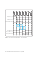
will be done in the memory and writeback stages. FIGURE 2-4 illustrates the SPARC
core pipeline and support structures.
Fetch
Thrd Sel
Decode
Execute
Regfile
x4
ICache
Itlb
Inst
buf x 4
Thrd
Sel
Mux
Thread selects
Thrd
Sel
Mux
FIGURE 2-4
Decode
Thread
select
logic
Memory
WB
Crypto
Coprocessor
Alu
Mul
Shft
Div
DCache
Dtlb
Stbuf x 4
Crossbar
Interface
Instruction type
Misses
Traps and interrupts
Resource conflicts
PC logic
x4
SPARC Core Pipeline and Support Structures
Chapter 2
SPARC Core
2-7
The instruction fill queue (IFQ) feeds into the I-cache. The missed instruction list
(MIL) stores the addresses that missed the I-cache and the ITLB, and the MIL feeds
into the load store unit (LSU) for further processing. The instruction buffer is two
levels deep, and it includes the thread instruction (TIR) and next instruction (NIR)
unit. Thread selection and scheduler (S-stage) resolves the arbitration among the
TIR, NIR, branch-PC, and trap-PC to pick one thread send it to the decode stage
(D-stage). FIGURE 2-5 shows the support structure for this portion of the thread
pipeline.
I-Cache
4x
TIR/
NIR
DEC
Schedule
ITLB
IFQ
4x
PC
MIL
br-pc/trap-pc
From
LSU
FIGURE 2-5
2.3.2
To
LSU
Frontend of the SPARC Core Pipeline
Instruction Fetch
The instruction fetch unit (IFU) maintains the program counters (PC) and the nextprogram counters (NPC) of all live instructions executed on the OpenSPARC T1
processor. For every SPARC core clock cycle, two instructions are fetched for every
instruction issued. This two fetches per one issue relationship is intended to reduce
the I-cache access in order to allow the opportunistic I-cache line fill. Each thread is
allowed to have one outstanding I-cache miss, and the SPARC core allows a total of
four I-cache misses. Duplicated I-cache misses do not induce the redundant fill
request to the level 2 cache (L2-cache).
2-8
OpenSPARC T1 Microarchitecture Specification • August 2006
2.3.3
Instruction Registers and Program Counter
Registers
In the instruction buffer, there are two instruction registers per thread – the thread
instruction register (TIR) and the next instruction register (NIR). The TIR contains
the current thread instruction in the thread selection stage (S-stage), and the NIR
contains the next instruction. An I-cache miss fill bypasses the I-cache and writes
directly to the TIR, but it never writes to the NIR.
The thread scheduler selects a valid instruction from the TIR. After selecting the
instruction, the valid instruction will be moved from the NIR to the TIR. If no valid
instruction exists in the TIR, a no operation (NOP) instruction will be inserted.
There is one program counter (PC) register per thread. The next-program counter
(NPC) could come from one of these sources:
1. Branch
2. TrapPC
3. Trap NPC
4. Rollback (a thread rolled back due to a load miss)
5. PC + 4
The IFU tracks the PC and NPC through W-stage. The last retired PC will be saved
in the trap logic unit (TLU), and, if a trap occurs, it will also be saved in the trap
stack.
2.3.4
Level 1 Instruction Cache
The instruction cache is commonly referred to as the level 1 instruction cache (L1I).
The L1I is physically indexed and tagged and is 4-way set associative with 16 Kbytes
of data. The cache-line size is 32 bytes. The L1I data array has a single port, and the
I-cache fill size is 16 bytes per access. The characteristics of cached data include –
32-bit instructions, 1-bit parity, and 1-bit predecode. The tag array also has a single
port.
There is a separate array for valid bit (V-bit). This V-bit array holds the cache line
state of either valid or invalid, and the array has one read port and one write port
(1R1W). The cache line invalidation only accesses the V-bit array, and the cache line
replacement policy is pseudo-random.
Chapter 2
SPARC Core
2-9
The read access to the I-cache has a higher priority over the write access. The ASI
read and write accesses to the I-cache are set to lower priorities. The completion of
the ASI accesses are opportunistic, and there is fairness mechanism built in to
prevent the starvation of service to ASI accesses.
The maximum wait period for a write access to the I-cache is 25 SPARC core clock
cycles. A wait longer than 25 clock cycles will stall the SPARC core pipeline in order
to allow the I-cache write access completion.
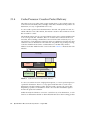
2.3.5
I-Cache Fill Path
I-cache fill packets come from the level 2 cache to processor interface (CPX) by way
of the load store unit (LSU). Parity and predecode bits will be calculated before the
I-cache fills up. CPX packets include invalidations (invalidation packets are nonblocking), test access point (TAP) reads and writes, and error notifications. The valid
bit array in the I-cache has a dedicated port for servicing the invalidation packets.
FIGURE 2-6 illustrates the I-cache fill path.
To
Vbit Ary
INV
To
Bypass
I-Cache to TIR
IFQ
bist>asi>cpx
bist asi
cpxpkt
from LSU
FIGURE 2-6
I-Cache Fill Path
The I-cache line size is 32 bytes, and a normal I-cache fill takes two CPX packets of
16 bytes each. The instruction fill queue (IFQ) has a depth of two. An I-cache line
will be invalidated when the first CPX packet is delivered and filled in the I-cache.
2-10
OpenSPARC T1 Microarchitecture Specification • August 2006
That cache line will be marked as valid when the second CPX packet is delivered
and filled. I-cache control guarantees the atomicity of the I-cache line fill action
between the two halves of the cache line being filled.
An instruction fetch from the boot PROM, by way of the system serial interface (SSI),
is a very slow transaction. The boot prom is a part of the I/O address space. All
instruction fetches from the I/O space are non-cacheable. The boot PROM fetches
only one 4-byte instruction at a time. This 4-byte instruction is replicated four times
during the formation of the CPX packet. Only one CPX packet of non-cacheable
instructions will be forwarded to the IFQ. The non-cacheable instructions fetched
from the boot PROM will not be filled in the I-cache. They will be sent to (or,
bypassed to) the thread instruction register (TIR) directly.
2.3.6
Alternate Space Identifier Accesses, I-Cache Line
Invalidations, and Built-In Self-Test Accesses to
the I-Cache
Alternate space identifiers (ASI) accesses to the I-cache, and the built-in self-test
(BIST) accesses to the I-cache, go through the IFQ data-path to the I-cache. All ASI
accesses and BIST accesses will cause the SPARC core pipeline to stall, so these
accesses are serviced almost immediately.
The load store unit (LSU) initiates all ASI accesses. The LSU serializes all ASI
accesses so that the second access will not be launched until the first access has been
acknowledged. ASI accesses tend to be slow, and data for an ASI read will be sent
back later.
A BIST operation requires atomicity, and it assumes and accommodates no
interruptions until it completes.
Level 2 cache invalidations will always undergo a CPU-ID check in order to ensure
that this invalidation packet is indeed meant for the specified SPARC core. In the
following cases, an invalidation could be addressing anyone:
■
A single I-cache line invalidation due to store acknowledgements, or due to a
load exclusivity requiring that the invalidation of the other level 1 I-caches
resulted from the self-modifying code.
■
Invalidating two I-cache lines because of a cache-line eviction in the level 2 cache
(L2-cache).
■
Invalidating all ways in a given set due to error conditions, such as encountering
a tag ECC error in a level 2 cache line.
Chapter 2
SPARC Core
2-11
2.3.7
I-Cache Miss Path
A missed instruction list (MIL) is responsible for sending the I-cache miss request to
the level 2 cache (L2-cache) in order to get an I-cache fill. The MIL has one entry per
thread, which supports a total of four outstanding I-cache misses for all four threads
in the same SPARC core at the same time. Each entry in the MIL contains the
physical address (PA) of an instruction that missed the I-cache, the replacement way
information, the MIL state information, the cacheability, the error information, and
so on. The PA tracks the I-fetch progress from the indication of an I-cache miss until
the I-cache has been filled. The dispatch of I-cache miss requests from different
threads follow a fairness mechanism based on a round-robin algorithm.
FIGURE 2-7 illustrates the I-cache miss path.
PA
Cmp
MIL
RR arb
pcxpkt
to LSU
FIGURE 2-7
I-Cache Miss Path
The MIL keeps track of the physical address (PA) of an instruction that missed the
I-cache. A second PA that matches the PA of an already pending I-cache miss will
cause the second request to be put on hold and marked as a child of the pending
I-cache miss request. The child request will be serviced when the pending I-cache
miss receives its response. The MIL uses a linked list to track and service the
duplicated I-cache miss request. The depth for such a linked list is four.
2-12
OpenSPARC T1 Microarchitecture Specification • August 2006
The MIL cycles through the following states:
1. Make request.
2. Wait for an I-cache fill.
3. Fill the first 16 bytes of data. The MIL sends a speculative completion notification
to the thread scheduler at the completion of filling the first 16 bytes.
4. Fill the second 16 bytes of data. The MIL sends a completion notification to the
thread scheduler at the completion of filling the second 16 bytes.
5. Done.
An I-cache miss request could be canceled because of, for example, a trap. The MIL
still goes through the motions of filling a cache line but it does not bypass it to the
thread instruction register (TIR). A pending child request must be serviced even if
the original parent I-cache miss request was cancelled.
When a child I-cache miss request crosses with a parent I-cache miss request, the
child request might not be serviced before the I-cache fill for the parent request
occurs. The child instruction fetch shall be retired (rolled back) to the F-stage to
allow it to access the I-cache. This kind of case is referred to as miss-fill crossover.
2.3.8
Windowed Integer Register File
The integer register file (IRF) contains 5 Kbytes of storage, and has three read ports,
2 write ports, and one transfer port (3R/2W/1T). The IRF houses 640 64-bit registers
that are protected by error correcting code (ECC). All read or write accesses can be
completed in one SPARC core clock cycle.
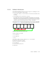
FIGURE 2-8 illustrates the structure of an integer architectural register file (IARF) and
an integer working register file (IWRF).
Chapter 2
SPARC Core
2-13
Architectural Set
(compact sram cells)
Working Set
(fast RF cells)
outs[0-7]
w(n+1)
call
locals[0-7]
outs[0-7]
ins[0-7]
w(n)
outs[0-7]
locals[0-7]
locals[0-7]
outs[0-7]
ins[0-7]
w(n-1)
locals[0-7]
Transfer
port
ins[0-7]
return
ins[0-7]
Read/Write
Access from pipe
FIGURE 2-8
IARF and IWRF File Structure
Each thread requires 128 registers for the eight windows (with 16 registers per
window), and four sets of global registers with eight global registers per set. There
are 160 registers per thread, and there are four threads per SPARC core. There are a
total of 640 registers per SPARC core.
Only 32 registers from the current window are visible to the thread. A window
change occurs in the background under thread switching while the other threads
continue to access integer register file.
Please refer to OpenSPARC T1 Processor Megacell Specification for additional details on
the IRF.
2-14
OpenSPARC T1 Microarchitecture Specification • August 2006
2.3.9
Instruction Table Lookaside Buffer
The instruction table lookaside butter (ITLB) is responsible for address translation
and tag comparison. The ITLB is always turned-on for non-hypervisor mode
operations, and the ITLB is always turned-off for hypervisor mode operations.
The ITLB contains 64 entries. The replacement policy is a pseudo least recently used
(pseudo-LRU) policy, which is the same policy as that for the I-cache.
The ITLB supports page sizes of 8 Kbytes, 64 Kbytes, 4 Mbytes, and 256 Mbytes.
Multiple hits in the ITLB are prevented by the autodemap feature in an ITLB fill.
2.3.10
Thread Selection Policy
Thread switching takes place during every SPARC core clock cycle. At the time of a
thread selection, the priority is given to the least recently executed yet available
thread. Load instructions will be speculated as cache hits and the thread executing a
load instruction will be deemed as available and allowed to be switched-in with a
low priority.
A thread could become unavailable due to one of these reasons:
1. The thread is executing one of the long latency instructions, such as load, branch,
multiplication, division, and so on.
2. The SPARC core pipeline has been stalled due to one of the long latency
operations, such as encountering a cache miss, taking a trap, or experiencing a
resource conflict.
Chapter 2
SPARC Core
2-15
2.3.11
Thread States
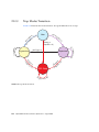
A thread cycles through these three different states – idle, active, and halt. FIGURE 2-9
illustrates the basic transition of non-active states.
es
um
e/
re s
et
Idle
intr
le
Id
int
r
Idle
r
any intr
Halt
Active
Halt inst
FIGURE 2-9
Basic Transition of Non-Active States
A thread is in an idle state at power-on. An active thread will only be transitioned to
an idle state after a wait mask for an I-cache fill has been cleared.
A thread in the idle state should not receive the resume command without a previous
reset. When a thread is violated, the integrity of the hardware behavior cannot be
guaranteed.
FIGURE 2-10 illustrates the thread state transition of an active thread.
2-16
OpenSPARC T1 Microarchitecture Specification • August 2006
d
is s
ld m
p/
tra
ule
ed
he
FIGURE 2-10
it c
Wait
sc
h
sw
com
ple
tio
n
Ready
ou
long lat/rsrc conflict
t
Run
Thread State Transition of an Active Thread
An active thread could be placed in the wait state because of any of the following
reasons:
1. Wait for an I-cache fill.
2. Wait due to store buffer full.
3. Wait due to long latency, or a resource conflict where all resource conflicts arise
because of long latency.
4. Wait due to any combination of the preceding reasons.
The current wait state is tracked in the IFU wait masks.
FIGURE 2-11 illustrates the state transition for a thread in speculative states.
Chapter 2
SPARC Core
2-17
schedule
Rdy
Run
lly done
Rea
Really d
one
s w it c h e d o u t
schedule
Wron
g
SpecRdy
sp
ec
SpecRun
S
pe
spec
g
n
ro
W
FIGURE 2-11
2.3.12
cu
la t
ed
one
Wait
rsrc
long lat/
t
flic
n
co
State Transition for a Thread in Speculative States
Thread Scheduling
A thread can be scheduled when it is in one of the following five states – idle (which
happens infrequently, and generally results from a reset or resume interrupt), Rdy,
SpecRdy, Run, and SpecRun. The thread priority in each state is different at the time
for scheduling. The priority scheme can be characterized as follows:
Idle > Rdy > SpecRdy > (Run = SpecRun)
The fairness scheme for threads in the Run state or the SpecRun state is a roundrobin algorithm with the least recently executed thread winning the selection.
Within Idle threads, the priority scheme is as follows:
T0 (thread 0) > T1 (thread 1) > T2 (thread 2) > T3 (thread 3)
2-18
OpenSPARC T1 Microarchitecture Specification • August 2006
2.3.13
Rollback Mechanism
The rollback mechanism provides a way of recovering from a scheduling error. The
two reasons for performing a rollback include:
1. All of the stall conditions, or switch conditions, were not known at the time of the
scheduling.
2. The scheduling was done speculatively on purpose.
For example, after issuing a load, the scheduler will speculate a level 1 D-cache
hit performance reasons. If the speculation was incorrect (because of encountering
a load miss), all of the instructions after the speculative load instruction must be
rolled back. Otherwise, the performance gain would be a substantial.
Rolled back instructions must be restarted from the S-stage or F-stage of the SPARC
core pipeline. FIGURE 2-12 illustrates the pipeline graph for the rollback mechanism.
F
FIGURE 2-12
S
D
E
M
W
Rollback Mechanism Pipeline Graph
The three rollback cases include:
1. E to S and D to F
2. D to S and S to F
3. W to F
The possible conditions causing a rollback case 1 or a case 2 include:
■
Instruction(s) following a load miss
■
Resource conflict due to long latency
■
Store buffer full
■
I-cache instruction parity error
■
I-fetch retry
Chapter 2
SPARC Core
2-19
The possible conditions causing rollback case 3 include:
2.3.14
■
Encountering an ECC error during the instruction register file access.
■
The floating-point store instruction encountering an ECC error during the
floating-point register file access.
■
Instruction(s) following a load hits the store buffer and the level 1 D-cache, where
the data has not been bypassed from the store buffer to the level 1 D-cache.
■
Encountering D-cache parity errors.
■
Launching an idle or resume interrupt where the machine states must be restored.
■
An interrupt has been scheduled but not yet taken.
Instruction Decode
The IFU decodes the SPARC V9 instructions, and the floating-point frontend unit
(FFU) decodes the floating-point instructions. Unimplemented floating-point
instructions will cause an fp_exception_other trap with a FSR.ftt=3
(unimplemented_FPop). These operations will be emulated by the software.
The privilege is checked in D-stage of the SPARC core pipeline. Some instructions
can only be executed with hypervisor privilege or with supervisor privilege.
The branch condition is also evaluated in the D-stage, and the decision for annulling
a delay slot is made in this stage as well.
2.3.15
Instruction Fetch Unit Interrupt Handling
All interrupts are delivered to the instruction fetch unit (IFU). For each received
interrupt, the IFU shall check the bit’s pstate.ie (the interrupt enable bit in the
processor state register) and hpstate (the hypervisor state) before scheduling the
interrupt. All interrupts will be prioritized (refer to the Programmer’s Reference
Manual for these priority assignments). Once prioritized, the interrupts will be
scheduled just like the instructions.
When executing in the hypervisor (HV) state, an interrupt with a supervisor (SV)
privilege will not be serviced at all. An hypervisor state execution shall not be
blocked by anything with supervisor privilege.
Nothing could block the scheduling of a reset, idle, or resume interrupt.
Some interrupts are asserted by a level while others are asserted by a pulse. The IFU
remembers the form the interrupts were originated in order to preserve the integrity
of the scheduling.
2-20
OpenSPARC T1 Microarchitecture Specification • August 2006
2.3.16
Error Checking and Logging
Parity protects the I-cache data and the tag arrays. The error correction action is to
re-fetch the instruction from the level 2 cache.
The instruction translation lookaside buffer (ITLB) array is parity decoded without
an error-correction mechanism, so all errors are fatal.
All on-core errors, and some of the off-core errors, are logged in the per-thread error
registers. Refer to the Programmer’s Reference Manual for details.
The instruction fetch unit (IFU) maintains the error injection and the error enabling
registers, which are accessible by way of ASI operations.
Critical states (such as program counter (PC), thread state, missed instruction list
(MIL), and so on) can be snapped and scanned out on-line. This process is referred
to as a shadow scan.
2.4
Load Store Unit
The load store unit (LSU) processes memory referencing operation codes (opcodes)
such as various types of loads, various types of stores, cas, swap, ldstub, flush,
prefetch, and membar. The LSU interfaces with all of the SPARC core functional
units, and acts as the gateway between the SPARC core units and the CCX. Through
the CCX, data transfer paths can be established with the memory subsystem and the
I/O subsystem (the data transfers are done with packets).
The threaded architecture of the LSU can process four loads, four stores, one fetch,
one FP operation, one stream operation, one interrupt, and one forward packet.
Therefore, thirteen sources supply data to the LSU.
The LSU implements the ordering for memory references, whether locally or not.
The LSU also enforces the ordering for all the outbound and inbound packets.
Chapter 2
SPARC Core
2-21
2.4.1
LSU Pipeline
There are four stages in the LSU pipeline. FIGURE 2-13 shows the different stages of
the LSU pipeline.
E
Cache
TLB
setup
FIGURE 2-13
M
Cache/Tag
TLB
read
W
stb lookup
traps
bypass
W2
pcx rcq gcn.
and writeback
LSU Pipeline Graph
The cache access set-up and the translation lookaside buffer (TLB) access set-up are
done during the pipeline’s E-stage (execution). The cache/tag/TLB read operations
are done in the M-stage (memory access). The W-stage (writeback) supports the
look-up of the store buffer, the detection of traps, and the execution of the data
bypass. The W2-stage (writeback-2) is for generating PCX requests and writebacks to
the cache.
2.4.2
Data Flow
The LSU includes an 8-Kbyte D-cache, which is a part of the level 1 cache shared by
four threads. There is one store buffer (STB) per thread. Stores are total store
ordering (TSO) ordered, that is to say that no membar #sync is required after each
store operation in order to maintain the program order among the stores. Non-TSO
compliant stores include – blk-store and blk-init. Bypass data are reported
asynchronously, and they are supported by the bypass queue.
Load misses are kept in the load miss (LSM) queue, which is shared by other
opcodes such as atomics and prefetch. The LSM queue supports one outstanding
load miss per thread. Load misses with duplicated physical addresses (PA) will not
be sent to the level 2 (L2) cache.
Inbound packets from the CCX are queued and ordered for distribution to other
units through the data fill queue (DFQ).
The DTLB is fully associative, and it is responsible for the address translations. All
CAM/RAM translations are single-cycle operations.
The ASI operations are serialized through the LSU. They are sequenced through the
ASI queue to the destination units on the chip.
FIGURE 2-14 illustrates the LSU data flow concept.
2-22
OpenSPARC T1 Microarchitecture Specification • August 2006
To ifu, etc
irf, frf
load
store
stb
dfq
array
tag
vld
tlb
pcx gen
From cpx
FIGURE 2-14
2.4.3
To pcx
LSU Data Flow Concept
Level 1 Data Cache (D-Cache)
The 8-Kbyte level 1 (L1) D-cache is 4-way set-associative, and the line size is 16
bytes. The D-cache has a single read and write port (1 RW) for the data and tag
array. The valid bit (V-bit) array is dual ported with one read port and one write port
(1R/1W). The valid bit array holds the cache line state of valid or invalid.
Invalidations access the V-bit array directly without first accessing the data and tag
array. The cache line replacement policy follows a pseudo-random algorithm, where
loads are allocating and stores non-allocating.
A cacheable load-miss will allocate a line, and it will execute the write-through
policy for stores. Stores do not allocate, and local stores may update the L1 D-cache
if it is present in the L1 D-cache, as determined by L2 (Level 2) cache directory. If it
is deemed that it is not present in L1 D-cache, the local stores will cause the lines to
become invalidated. The line replacement policy is pseudo random based on a linear
shift register. The data from the bypass queues will be multiplexed into the L1 Dcache in order to be steered to the intended destination. The D-cache supports up to
four simultaneous invalidates from the data evictions.
Chapter 2
SPARC Core
2-23
The L2-cache is always inclusive of the L1 D-cache. The exclusivity of the D-cache
dictates that a line present in the L1 D-cache will not be present in the L1 I-cache.
The data valid array is dual ported with one read port and one write port (1R1W).
Each line in the L1 D-cache is parity protected. A parity error will cause a miss in the
L1 D-cache which, in turn, will cause the correct data to be brought back from the
L2-cache.
In addition to the pipeline reads, the L1 D-cache can also be accessed by way of
diagnostic ASI operations, BIST operations, and RAMtest operations through the test
access port (TAP).
2.4.4
Data Translation Lookaside Buffer
The data translation lookaside buffer (DTLB) is the TLB for the D-cache. The DTLB
caches up to the 64 most-recently-accessed translation table entries (TTE) in a fully
associative array. The DTLB has one CAM port and one read-write port (1 RW). All
four threads share the DTLB. The translation table entries of each thread are kept
mutually exclusive from the entries of the other threads.
The DTLB supports the following 32-bit address translation operations:
■
VA -> PA [virtual address (VA) to physical address (PA) translation]
■
VA = PA [address bypass for hypervisor mode operations]
■
RA -> PA [Real Address (RA) to Physical Address (PA) bypass translation for
supervisor mode operations]
The TTE tag and the TTE data are both parity protected and errors are uncorrectable.
TTE access parity errors for load instructions will cause a precise trap. TTE access
parity errors for store instructions will cause a deferred trap (that is, the generation
of the trap will be deferred to the instruction following the store instruction).
However, the trap PC delivered to the system software still points to the store
instruction that encountered the parity error in the TTE access. Therefore, the
deferred action of the trap generation will still cause a precise trap from the system
software perspective.
2-24
OpenSPARC T1 Microarchitecture Specification • August 2006
2.4.5
Store Buffer
The physical structure of the store buffer (STB) consists of a store buffer CAM (SCM)
and a store buffer data array (STBDATA). Each thread is allocated with eight fixed
entries in the shared data structures. The SCM has one CAM port and one RW port,
and the STBDATA has one read (1R) port and one write (1W) port.
All stores reside in the store buffer until they are ordered following a total store
ordering (TSO) model and have updated the L1D (level 1 D-cache). The lifecycle of a
TSO compliant store follows these four stages:
1. Valid
2. Commit (issued to L2-cache)
3. Acknowledged (L2-cache sent response)
4. Invalidated or L1D updated
Non-TSO complaint stores, such as blk-init and other flavors of bst (block store), will
not follow the preceding life-cycle. A response from the L2-cache is not required
before releasing the non-TSO complaint stores from the store buffer.
Atomic instructions such as CAS, LDSTUB, and SWAP, as well as flush instructions,
can share the store buffer.
The store buffer implements partial and full read after write (RAW) checking. FullRAW data will be returned to the register files from the pipe. Partial RAW hits will
force the load to access the L2-cache while interlocked with the store issued to the
CCX. Multiple hits in the store buffer will always force access to the L2-cache in
order to enforce data consistency.
If a store hits any part of a quad-load (16-byte access), the quad-load checking will
force the serialization of the issue to the CCX. This forced serialization enforces that
there will be no bypass operation.
Instructions such as a blk-load (64-byte access) will not detect the potential store
buffer hit on the 64-byte boundary. The software must guarantee the data
consistency using membar instructions.
Chapter 2
SPARC Core
2-25
2.4.6
Load Miss Queue
The load miss queue (LMQ) contains four entries in its physical structure, and the
queue supports up to one load miss per thread. Instructions similar to load (such as
atomics and prefetches) may also reside in the load miss queue.
A load instruction speculates on a D-cache miss to reduce the latency in accessing
the CCX. The load instruction may also speculate on the availability of a queue entry
in the CCX. If the speculation fails, the miss-speculated load instruction can be
replayed out of LMQ.
Load requests to the L2-cache from different addresses can alias to the same L2cache line. Primary versus secondary checking will be performed in order to prevent
potential duplication in the L2-cache tags.
The latencies for completing different load instructions may differ (for example, a
quad-load fill will have to access integer register file (IRF) twice).
The LMQ is also leveraged by other instructions. For example, the first packet of a
CAS instruction will be issued out of the store buffer while the second packet will be
issued out the LMQ.
2.4.7
Processor to Crossbar Interface Arbiter
The processor-to-crossbar interface (PCX) is the interface between the processor and
the CCX. The arbiter takes on 13 sources to produce one arbitrated output in one
cycle. The 13 sources include – four load-type instructions, four store-type
instructions, one instruction cache (I-cache) fill, one floating-point unit (FPU) access,
one stream processing unit (SPU) access, one interrupt, and one forward-packet.
The 13 sources are further divided into four categories of different priorities. The
I-cache miss handling is one category. The load instructions (one outstanding per
thread) are in one category. The store instructions (one outstanding per thread) are in
another category. The rest of accesses are lumped into one category, and include –
the FPU access, SPU access, interrupt, and the forward-packet.
The arbitration is done within the category first and then among the other
categories. An I-cache fill is at the highest priority, while all other categories have an
equal priority. The priorities can be illustrated in this order:
1. I-cache miss
2. Load miss
3. Stores
4. {FPU operations, SPU operations, Interrupts}
2-26
OpenSPARC T1 Microarchitecture Specification • August 2006
The use of a two-level history allows a fair, per-category scheduling among the
different categories. The arbiter achieves a resolution in every cycle. Requests from
atomic instructions take two cycles to finish the arbitration.
There are five possible targets, which include four L2-cache banks and one I/O
buffer (IOB). The FPU access shares the path through the IOB.
Speculation on the PCX availability does occur, and a history will be established
once the speculation is known to be correct.
2.4.8
Data Fill Queue
A SPARC core communicates with memory and I/O using packets. The incoming
packets, destined to a SPARC core, are queued in the data fill queue (DFQ) first.
These packets can be acknowledgement packets or data packets from independent
sources. The DFQ maintains a predefined ordering requirement for all the inbound
packets. The targets for the DFQ to deliver the packets to include the instruction
fetch unit (IFU), load store unit (LSU), trap logic unit (TLU), and stream processing
unit (SPU).
A store to the D-cache is not allowed to bypass another store to the D-cache. Store
operations to different caches can bypass each other without violating the total store
ordering (TSO) model.
Interrupts are allowed to be delivered to TLU only after all the prior invalidates
have been visible in their respective caches. An acknowledgement to a local I-flush is
treated the same way as an interrupt.
Streaming stores will be completed to the D-cache before the acknowledgement is
sent to the SPU.
2.4.9
ASI Queue and Bypass Queue
Certain SPARC core internal alternate space identifier (ASI) accesses, such as the
long latency MMU ASI transactions and all IFU ASI transactions, are queued in the
ASI queue. The ASI queue is a FIFO that supports one outstanding ASI transaction
per thread. For all read-type ASI transactions, regardless whether they originated
from the LSU or not, must have their the return data routed through the LSU and be
delivered to the register file by way of the bypass queue.
The bypass queue handles all of the load reference data, other than that received
from the L2-cache, that must be asynchronously written to the integer register file
(IRF). This kind of read data includes full-RAW data from the store buffer, ldxa to the
internal ASI data, store data for casa, a forward packet for the ASI transactions, as
well as the pending precise traps.
Chapter 2
SPARC Core
2-27
2.4.10
Alternate Space Identifier Handling in the Load
Store Unit
In addition to sourcing alternate space identifier (ASI) data to other functional units
of a SPARC core, the load store unit (LSU) decodes and supports a variety of ASI
transactions, which include:
2.4.11
■
Defining the behavior of ld/st ASI transactions such as blk-ld, blk-st, quad-ASI,
and so on
■
Defining an explicit context for address translation at all levels of privilege, such
as primary, secondary, as_if_user, as_if_supv, and so on
■
Defining special attributes, such as non_faulting and endianness, and so on
■
Defining address translation bypassed, such as [RA=PA], [VA=PA], and so on,
where VA stands for virtual address, PA stands for physical address, and RA
stands for real address
Support for Atomic Instructions (CAS, SWAP,
LDSTUB)
CAS is issued as a two-packet sequence to the Processor to L2-cache Interface (PCX).
Packet 1 contains the compare address (rs1) and the data (rs2). Packet 2 contains the
swap data (rd). Packet 1 resides in the store buffer in order to be compliant to the
TSO ordering, while Packet 2 occupies the thread’s entry into the load miss queue
(LMQ).
Packet 1 and Packet 2 are issued in back-to-back order to the PCX. An
acknowledgement to the load is returned to the CPX in response to Packet 1.
This acknowledgment contains the data in memory from the address-in (rs1). An
acknowledgement to the store is returned on the CPX in response to Packet 2. This
acknowledgement will cause an invalidation at address-in (rs1) if the cache line is
present in the level 1 D-cache.
SWAP and LDSTUB are single packet requests to the PCX, and they reside in the
store buffer.
2-28
OpenSPARC T1 Microarchitecture Specification • August 2006
2.4.12
Support for MEMBAR Instructions
MEMBAR instructions ensure that the store buffer of a thread has been drained
before the thread gets switched back in. The completion of draining the store buffer
implies that all stores prior to the MEMBAR instruction have reached a global
visibility, in compliance with TSO ordering. Before a MEMBAR is released, it ensures
that all blk-init and blk-st instructions have also reached global visibility. This is
accomplished by making sure that st-ack counter has been cleared.
There are several flavors of MEMBAR instructions. The implementation for
#storestore, #loadstores, and #loadload is to make them behave like NOPs. The
implementation for #storeload, #memissue, and #lookaside is to make them to
behave like #sync. membar #sync is fully implemented to help enforce the compliance
to TSO ordering.
A parity error on a store to the DTLB will cause a deferred trap. It will be reported
on the follow-up membar #sync. The trap PC in this case will point to the store
instruction encountering the parity error when storing to the DTLB. The deferred
trap will look like a precise trap to the system software because of the way the
hardware supports the recording of the precise trap PC.
2.4.13
Core-to-Core Interrupt Support
A core-to-core interrupt is initiated by a write to the interrupt dispatch register
IINT_VEC_DIS ASI) in Trap Logic Unit (TLU). It will generate a request to LSU for
access to PCX. LSU only supports one outstanding interrupt request at any time.
An interrupt is treated similar to a membar. It will be sent to PCX once the store
buffer of the corresponding thread has been drained. This interrupt will then
immediately be acknowledged to TLU.
After the interrupt packet has been dispatched by way of the L2-cache to Core
Interface (CCX), the packet would be executed on the destination thread of a SPARC
core. It can be invalidated after all prior invalidates have completed and results
arrived at L1 D-cache (L1D).
2.4.14
Flush Instruction Support
A flush instruction does not actually flush the instruction memory. It instead, it acts
as a barrier to ensure that all of the prior invalidations for a thread have been visible
in the level 1 I-cache (L1I) before causing the thread to be switched back in.
The flush is issued as an interrupt with the flush bit set, which causes the L2-cache
to broadcast the packet to all SPARC cores.
Chapter 2
SPARC Core
2-29
For the SPARC core that issued the flush, an acknowledgement from the DFQ upon
receiving the packet will cause all of the prior invalidations to complete with the
results arrived at the level 1 I-cache and the level 1 D-cache (L1 I/D).
For the SPARC cores that did not issue the flush, the DFQ will serialize the flushes
so that the order of the issuing threads actions, relative to the flushes, will be
preserved.
2.4.15
Prefetch Instruction Support
A prefetch instruction is treated as a non-cacheable load. A prefetch that misses in
the TLB, or accesses I/O space, will be treated as a NOP. The issuing thread will be
switched back in without accessing the processor to L2-cache interface (PCX).
The LSU supports a total of eight outstanding prefetch instructions across all four
threads. The LSU keeps track of the number of outstanding prefetches per thread,
which limits the number of outstanding prefetches.
2.4.16
Floating-Point BLK-LD and BLK-ST Instructions
Support
Floating-point blk-ld and blk-st instructions are non-TSO compliant. Only one
outstanding blk-ld or blk-st instruction is allowed per SPARC core. These
instructions will bypass the level 1 caches and will not allocate in the level 1 caches
either. On a level 1 D-cache (L1D) hit, a blk-st instruction will cause an invalidation
to the L1D. Both blk-st and blk-ld instructions can access the memory space and the
I/O space.
The LSU breaks up a the 64-byte packet of a blk-ld instruction into four of 16-byte
load packets so that they can access the processor and L2-cache interface (PCX). The
Level 2 cache returns four of the 16-byte packets, which in turn, will cause eight of 8byte data transfers to the floating-point register file (FRF). Errors are reported on the
last packet. A blk-ld instruction could cause a partial update to the FRF. Software
must be written to retry the instruction later.
A blk-st instruction will be unrolled into eight helper instructions by the floatingpoint functional unit (FFU) for a total of a 64-byte data transfer. Each 8-byte data
gets an entry of the corresponding thread in the store buffer. The blk-st instructions
are non-TSO compliant, so the software must do the ordering.
2-30
OpenSPARC T1 Microarchitecture Specification • August 2006
2.4.17
Integer BLK-INIT Loads and Stores Support
The blk-init load and blk-init store instructions were introduced as the substitute for
blk-ld and blk-st in block-copy routines. They can access both the memory space and
the I/O space. The blk-init loads do not allocate in the level 1 D-cache. On a level 1
D-cache hit, the blk-init stores will invalidate the level 1 D-cache (L1D).
The blk-init load instructions must be quad-word accesses, and violating this rule
will cause a trap. Like quad-load instructions, blk-init loads also send double-pump
writes (8-byte access) to the integer register file (IRF) when a blk-init load packet
reaches the head of the data fill queue (DFQ).
The blk-init stores are also non-TSO compliant, which allows for greater write
throughput and higher-performance yields for the block-copy routine.
Up to only eight of all non-TSO compliant instructions can be allowed outstanding
for each SPARC core. The LSU keeps a counter per thread to enforce this limit.
2.4.18
STRM Load and STRM Store Instruction Support
Instructions such as strm-ld and strm-st make requests from the stream processing
unit (SPU) to memory by way of the LSU.
The Store buffer will not be looked-up by the strm-ld instructions, and the store
buffer will not buffer strm-st data. Software must be written to enforce the ordering
and the maintenance of the data coherency.
The acknowledgements for strm-st instructions will be ordered through the data fill
queue (DFQ) upon the return to the stream processing unit (SPU). The
corresponding store acknowledgement (st ack) will be sent to the SPU once the
level 1 D-cache (L1D) invalidation, if any, has been completed.
2.4.19
Test Access Port Controller Accesses and Forward
Packets Support
Test access port (TAP) controller can access any SPARC core by way of the SPARC
interface of the I/O bridge (IOB). A forward request to the SPARC core might take
any of the following actions:
■
■
■
■
Read or write level 1 I-cache or D-cache
Read or write BIST control
Read or write margin control
Read or write de-feature bits to the de-feature any, or all, of L1I, L1D, ITLB, DTLB
in order to take a cache off-line, or a TLB offline, for diagnostic purposes
Chapter 2
SPARC Core
2-31
A forward reply will be sent back to the I/O bridge (IOB) once the data is read or
written. A SPARC core might further forward the request to the L2-cache for an
access to the control status register (CSR). The I/O bridge only supports one
outstanding forward access at any time.
2.4.20
SPARC Core Pipeline Flush Support
A SPARC core pipeline flush is reported through the LSU since the LSU is the source
of the latest traps in the pipeline.
The trap logic unit (TLU) gathers traps from all functional units except the LSU, and
it then sends them to the LSU. the LSU performs the or function for all of them (plus
its own) and then it broadcasts across the entire chip.
The LSU can also send a truncated flush for the internal ASI ld/st to the TLU, the
MMU, and the SPU.
2.4.21
LSU Error Handling
Errors can be generated from any, or all, of the following memory arrays – DCACHE
(D-cache), D-cache tag array (DTAG), D-cache valid bit array (DVA), DTLB, data fill
queue (DFQ), store buffer CAM array (SCM), and store buffer data array
(STBDATA). Only the DCACHE, DTAG, and DTLB arrays are parity protected.
2-32
■
A parity error on a load reference to the DCACHE will be corrected by way of the
reloading the correct data from the L2-cache as if there were a D-cache miss.
■
A DTAG parity error will result in a correction packet, followed by the actual load
request, to the L2-cache. The correction packet synchronizes the L2 directory and
the L1 D-cache set. On the load request acknowledgement, the level 1 D-cache
will be filled.
■
A parity error on the DTLB tte-data will cause an uncorrectable error trap to the
originating loads or stores.
■
A parity error on the DTLB tte-data can also cause an uncorrectable error trap for
ASI reads.
■
A parity error on the DTLB tte-tag can only cause an uncorrectable error trap for
ASI reads.
OpenSPARC T1 Microarchitecture Specification • August 2006
2.5
Execution Unit
The execution unit (EXU) contains these four subunits – arithmetic and logic unit
(ALU), shifter (SHFT), integer multiplier (IMUL), and integer divider (IDIV).
FIGURE 2-15 presents a top level diagram of the execution unit.
WR
MUL
rd to RF
Load
data
data
to LSU
rs3
reg addr
rs1
Register
file
rs2
rs3
thread,
window controls
rs1, rs2
DIV
Bypass
Logic
W
M
E
imn
ALU
oncode
addr
to LSU
rd to RF
ECL
SHFT
FIGURE 2-15
Execution Unit Diagram
The execution control logic (ECL) block generates the necessary select signals that
control the multiplexors, keeps track of the thread and reads of each instruction, and
implements the bypass logic. The ECL also generates the write-enables for the
integer register file (IRF). The bypass logic block does the operand bypass from the
E, M, and W stages to the D stage. Results of long latency operations such as load,
mul, and div, are forwarded from the W stage to the D stage. The condition codes
are bypassed similar to the operands, and bypassing of the FP results and writes to
the status registers are not allowed.
The shifter block (SHFT) implements the 0 - 63-bit shift, and FIGURE 2-16 illustrates
the top level block diagram of the shifter.
Chapter 2
SPARC Core
2-33
right shift
32b
mask/sign
extend
selec
left shift
FIGURE 2-16
Shifter Block Diagram
The arithmetic and logic unit (ALU) consists of an adder and logic operations such
as – ADD, SUB, AND, NAND, OR, NOR, XOR, XNOR, and NOT. The ALU is also
reused when calculating the branch address or a virtual address. FIGURE 2-17
illustrates the top level block diagram of the ALU.
Exu_ifu_brpc_e
Add/sub
Result Select Mux
cc. C, V
sum
Sum predict
shft result
PR or SR output
logic
Logic
=0?
=0?
FIGURE 2-17
2-34
regz
ALU Block Diagram
OpenSPARC T1 Microarchitecture Specification • August 2006
cc.Z
MUL is the integer multiplier unit (IMUL), and DIV is the integer divider unit
(IDIV). IMUL includes the accumulate function for modular arithmetic. The latency
of IMUL is 5 cycles, and the throughput is 1-half per cycle. IMUL supports one
outstanding integer multiplication operation per core, and it is shared between a
SPARC core pipeline and the modular arithmetic unit (MAU). The arbitration is
based on a round-robin algorithm.
IDIV contains a simple non-restoring divider, and it supports one outstanding
divide operation per core.
FIGURE 2-18 illustrates the top level diagram of the IDIV.
1 bit left shift
Dividend/
Quotient
Input
Queue
FIGURE 2-18
XOR
+
Divisor
IDIV Block Diagram
When either IMUL or IDIV is occupied, a thread issuing a MUL or DIV instruction
will be rolled back and switched out.
2.6
Floating-Point Frontend Unit
2.6.1
Functional Description of the FFU
The floating-point frontend unit (FFU) is responsible for dispatching floating-point
operations (FP ops) to the floating-point unit (FPU) through the LSU, as well as
executing simple FP ops (mov, abs, neg) and VIS instructions. The FFU also
maintains the floating-point state register (FSR) and the graphics state register
(GSR). There can be only one outstanding instruction in the FFU at a time.
Chapter 2
SPARC Core
2-35
The FFU is composed of four blocks – the floating-point register file (FFU_FRF), the
control block (FFU_CTL), the data-path block (FFU_DP), and the VIS execution block
(FFU_VIS). FIGURE 2-19 shows a block diagram of the FFU illustrating these four subblocks.
FFU_CTL
ren
wen
addr
2
7
78
FRF
dout
78
FFU_DP
FFU_VIS
din
ST/FPop Load
Data to data
LSU
FIGURE 2-19
2.6.2
FPU
result
Top-Level FFU Block Diagram
Floating-Point Register File
The floating-point register file (FRF) has 128 entries of 64-bits of data, plus 14-bits of
ECC. The write port has an enable for each half of the data. Bits [38:32] are the ECC
bits for the lower word (data[31:0]) and bits [77:71] are the ECC bits for the upper
word (data[70:39]).
2.6.3
FFU Control (FFU_CTL)
The FFU control (FFU_CTL) block implements the control logic for the FFU, and it
generates the appropriate multiplexor selects and data-path control signals. The FFU
control also decodes the fp_opcode and contains the state machine for the FFU
pipeline. It also generates the FP traps and kill signals, as well as signalling the LSU
when the data is ready for dispatch.
2-36
OpenSPARC T1 Microarchitecture Specification • August 2006
2.6.4
FFU Data-Path (FFU_DP)
This FFU data-path block contains the multiplexors and the flops for the data that
has been read from, or is about to be written to, the FRF. The FFU data-path also
dispatches the data for the STF and the FPops to the LSU, receives LDF from the
LSU, and receives the results from the FPops from the CPX. The FFU data-path also
implements FMOV, FABS, and FNEG, checks the ECC for the data read from the
FRF, and generates the ECC for the data written to the FRF.
2.6.5
FFU VIS (FFU_DP)
The FFU VIS (FFU_DP) block implements a subset of the VIS graphics instructions,
including partitioned addition/subtraction, logical operations, and faligndata. All
the operations are implemented in a single cycle, and the data inputs and outputs
are connected to the FFU_DP.
2.7
Multiplier Unit
2.7.1
Functional Description of the MUL
The SPARC multiplier unit (MUL) performs the multiplication of two 64-bit inputs.
The MUL is shared between the EXU and the SPU, and it has a control block and
data-path block. FIGURE 2-20 shows how the multiplier is connected to other
functional blocks.
sparc_mul_top
Data In/Control
EXU
FIGURE 2-20
Data Out
Data In/Control
SPU
Multiplexor (MUL) Block Diagram
Chapter 2
SPARC Core
2-37
2.8
Stream Processing Unit
Each SPARC core is equipped with a stream processing unit (SPU) supporting the
asymmetric cryptography operations (public-key RSA) for up to a 2048-bit key size.
The SPU shares the integer multiplier with the execution unit (EXU) for the modular
arithmetic (MA) operations. The SPU itself supports full modular exponentiation.
While the SPU facility is shared among all threads of a SPARC core, only one thread
can use the SPU at a time. The SPU operation is set up by a storing a thread to a
control register and then returning to normal processing. The SPU will initiate
streaming load or streaming store operations to the level 2 cache (L2) and compute
operations to the integer multiplier. Once the operation is launched, it can operate in
parallel with SPARC core instruction execution. The completion of the operation is
detected by polling (synchronous fashion) or by interrupt (asynchronous fashion).
2.8.1
ASI Registers for the SPU
All alternate space identifier (ASI) registers for the SPU are 8 bytes in length. Access
to all of the ASI registers for the SPU have hypervisor privilege, so they can only be
accessed in hypervisor mode. The following list highlights those ASI registers.
■
Modular arithmetic physical address (MPA) register
This register carries the physical address used to access the main memory.
MA_LD requests must be on the 16-byte boundary while MA_ST requests must
be on the 8-byte boundary.
■
Modular arithmetic memory addresses (MA_ADDR) register
This register carries the memory address offsets for various operands, and the
size of the exponent. FIGURE 2-21 highlights the layout of the bit fields.
[63:48]
RSVD
[47:40] [39:32]
ES
E
X
FIGURE 2-21
■
[31:24] [23:16]
X
M
[15:8]
[7:0]
N
M
A
MA_EXP
N
B
A
MA_MUL
R
N
A
MA_RED
Layout of MA_ADDR Register Bit Fields
Modular arithmetic N-prime value (MA_NP) register
This register is used to specify the modular arithmetic N-prime value.
2-38
OpenSPARC T1 Microarchitecture Specification • August 2006
■
Modular arithmetic synchronization (MA_SYNC) register
A load operation from this register is used to synchronize a thread with the
completion of asynchronous modular arithmetic operations performed by the
SPU.
■
Modular arithmetic control parameters (MA_CTL) register
This register contains several bit-filed fields that provide these control
parameters:
■
PerrInj – Parity error injection
When this parameter is set, each operation that writes to modular arithmetic
memory will have the parity bit inverted.
■
Thread – Thread ID for receiving interrupt
If the Int bit is set, this set of bits specifies the thread that will receive the
disrupting trap on the completion of the modular arithmetic operation.
■
Busy – SPU is BUSY
When this parameter is set, the SPU is busy working on the specified
operation.
■
Int – Interrupt enable
When this parameter is set, the SPU will generate a disrupting trap to the
current thread on completion of the current modular arithmetic operation. If
cleared, software can synchronize with the current modular arithmetic
operation using the MA_Sync instruction.
The disrupting trap will use the implementation_dependent_exception_20 as the
modular arithmetic interrupt.
■
Opcode – Operation code of modular arithmetic operation (see TABLE 2-3)
TABLE 2-3
Modular Arithmetic Operations
Opcode Value
Modular Arithmetic Operation
0
Load from modular arithmetic memory
1
Store to modular arithmetic memory
2
Modular multiply
3
Modular reduction
4
Modular exponentiation loop
5-7
Reserved
■
Length – Length of modular arithmetic operations
This field contains the bits for the value of the (length - 1) for the modular
arithmetic operations.
Chapter 2
SPARC Core
2-39
2.8.2
Data Flow of Modular Arithmetic Operations
FIGURE 2-22 illustrates the data flow of modular arithmetic operations.
SPU
MUL
IFU
SPU_MAMEM
(bw_r_idct)
SPU_CTL
EXU
TLU
SPU_MADP
LSU
CPX
FIGURE 2-22
2.8.3
Data Flow of Modular Arithmetic Operations
Modular Arithmetic Memory (MA Memory)
A total of 1280 bytes of local memory with a single read/write port (1RW) is used to
supply operands to modular arithmetic operations. The modular arithmetic memory
(MA memory) will house 5 operands with 32 words each, which supports a
maximum key size of 2048 bits. This MA memory is parity protected with a 2-bit
parity for each 64-bit word.
MA memory requires software initialization prior to the start of MA memory
operations. Three MA_LD operations are required to initialize all 160 words of
memory because the MA_CTL length field allows up to 64 words to be loaded into
MA memory.
Write accesses to the MA memory can be on either the 16-byte boundary or the
8-byte boundary. Read accesses to the MA memory must be on the 8-byte boundary.
2-40
OpenSPARC T1 Microarchitecture Specification • August 2006
2.8.4
Modular Arithmetic Operations
All modular arithmetic registers must be initialized prior to launching a modular
arithmetic operation. Modular arithmetic operations (MA ops) start with a stxa to
the MA_CTL register if the store buffer for that thread is empty. Otherwise, the
thread will wait until the store buffer is emptied before sending stx_ack to the LSU.
An MA operation that is in progress can be aborted by another thread by way of a
stx to the MA_CTL register.
An ldxa to MA registers are blocking. All except ldxa to the MA_Sync register will
respond immediately. An ldxa to the MA_Sync register will return a 0 to the
destination register upon the operation completion. The thread ID of this ldxa
should be equal to that stored in the thread ID field of the MA_CTL register.
Otherwise, the SPU will respond immediately and send signals to the LSU to not
update the register file. In case of aborting an MA operation, the pending ldxa to
MA_Sync is unblocked, and the SPU signals the LSU will not update the register file.
FIGURE 2-23 illustrates the MA operations using a state transition diagram.
ma_op
Idle
Abort
Wait
FIGURE 2-23
State Transition Diagram Illustrating MA Operations
Chapter 2
SPARC Core
2-41
The state transitions are clarified by the following set of equations:
tr2_maop_frm_idle = cur_idle & stxa_2ctlreq & ~wait_4stb_empty & ~wait_4trapack_set;
tr2_abort_frm_maop = cur_maop & stxa_2ctlreg;
tr2_wait_frm_abort = cur_abort & ma_op_complete;
tr2_maop_frm_wait = cur_wait & ~(stxa_2ctlreg | wait_4stb_empty | wait_4trapack_set);
tr2_idl_frm_maop = cur_maop & ~stxa_2cltreg & ma_op_complete;
tr2_wait_frm_idle = cur_idle & stxa_2ctlreg & (wait_4stb_empty | wait_4trapack_set);
A MA_ST operation is started with a stxa to the MA_CTL register opcode equals the
MA_ST, and the length field specifies the number of words to send to the level 2
cache (L2-cache). The SPU sends a processor to cache interface (PCX) request to the
LSU and waits for an acknowledgement from the LSU prior to sending another
request. If needed, store acknowledgements, which are returned from the L2-cache
on level 2 cache to processor interface (CPX), will go to the LSU in order to
invalidate the level 1 D-cache (L1D). The LSU will then send the SPU an
acknowledgement. The SPU then decrements a local counter and waits for all the
stores sent out to be acknowledged and transitioned to the done state.
On a read from the MA Memory, the operation will be halted if a parity error is
encountered. The SPU waits for all posted stores to be acknowledged. If the Int bit is
cleared (Int = 0), the SPU will signal the LSU and the IFU on all ldxa to the MA
registers.
An MA_LD operation is started with a stxa to MA_CTL register opcode equals
MA_LD, and the length field specifies the number of words to be fetched from the
L2-cache. The SPU sends a PCX request to the LSU and waits for an
acknowledgement from the LSU before sending out another request. The L2-cache
returns data to the SPU directly on CPX.
Any data returned with an uncorrectable error will halt the operation. If the Int bit is
cleared (Int = 0), the SPU will send a signal to the LSU and the IFU on any ldxa to
MA register.
Any data returned with a correctable error will cause the error address to be sent to
IFU and be logged, while the operation will continue until completion.
TABLE 2-4 illustrates the error handling behavior.
TABLE 2-4
2-42
Error Handling Behavior
NCEEN
Int
LSU
IFU
0
0
-
error_log
0
1
-
error_log
1
0
precise trap
error_log
1
1
-
error_log
OpenSPARC T1 Microarchitecture Specification • August 2006
The MA_MUL, MA_RED, and the MA_EXP operations all started with a stxa to
MA_CTL register with an opcode equal to the respective operation, and the length
field specifies the number of 64-bit words for each operation. The maximum length
of these operations should never exceed 32 words.
The MA_MUL operates on A, B, M, N and N operands. The result will be stored in
the X operand.
The MA_RED operates on A and N operands and the result will be stored in the R
operand.
The MA_EXP performs the inner loop of modular exponentiation of A, M, N, X, E,
operands stored in the MA Memory. This is the binary approach where the
MA_MUL, followed by MA_RED functions, are called and will have the results
stored in X operand.
The parity error encountered on an operand read will cause the operation to be
halted. The LSU and the IFU will be signaled.
FIGURE 2-24 shows a pipeline diagram that illustrates the sequence of the result
generation of the multiply function.
oprnd1
oprnd2
mul_ack
mul_res
oprnd1
oprnd2
mul_res
mul_ack
FIGURE 2-24
2.9
Multiply Function Result Generation Sequence Pipeline Diagram
Memory Management Unit
The memory management unit (MMU) maintains the contents of the instruction
translation lookaside buffer (ITLB) and the data translation lookaside buffer (DTLB).
The ITLB resides in instruction fetch unit (IFU), and the DTLB resides in load and
store unit (LSU). FIGURE 2-25 shows the relationship among the MMU and the TLBs.
Chapter 2
SPARC Core
2-43
IFU
LSU
ITLB
DTLB
MMU
FIGURE 2-25
2.9.1
MMU and TLBs Relationship
The Role of MMU in Virtualization
The OpenSPARC T1 processor provides hardware support for the virtualization
where multiple images and/or instances of the operating system (OS) coexist on top
of the underlying chip multiple threading (CMT) microprocessor.
FIGURE 2-26 illustrates the view of virtualization.
Applications
OS instance 1
OS instance 2
Hypervisor
OpenSPARC T1
FIGURE 2-26
2-44
Virtualization Diagram
OpenSPARC T1 Microarchitecture Specification • August 2006
The hypervisor (HV) layer virtualizes the underlying central processing units (CPU).
The multiple instances of the OS images form multiple partitions of the underlying
virtual machine. The hypervisor improves the OS portability to the new hardware
and insures that failure in one domain would not affect the operation in the other
domains. The OpenSPARC T1 processor supports up to eight partitions, and the
hardware provides 3 bits of partition ID in order to distinguish one partition from
another.
The hypervisor (HV) layer uses physical addresses (PA) while the supervisor (SV)
layer views real addresses (RA) where the RAs represent a different abstraction of
the underlying PAs. All applications use virtual addresses (VA) to access memory.
(The VA will be translated to RA and then to PA by TLBs and the MMU.)
2.9.2
Data Flow in MMU
The MMU interacts with TLBs to maintain the content of TLBs. The system software
manages the content of MMU by way of three kinds of operations – reads, writes,
and demap. All TLB entries are shared among the threads, and the consistency
among the TLB entries is maintained through auto-demap. The MMU is responsible
for generating the pointers to the software translation storage buffers (TSB), and it
also maintains the fault status for the various traps.
The access to the MMU is through the hypervisor-managed ASI operations such as
ldxa and stxa. These ASI operations can be asynchronous or in-pipe, depending on
the latency requirements. Those asynchronous ASI reads and writes will be queued
up in LSU. Some of the ASI operations can be updated through faults or by a data
access exception. Fault data for the status registers will be sent by trap logic unit
(TLU) and the load and store unit (LSU).
2.9.3
Structure of Translation Lookaside Buffer
The translation lookaside buffer (TLB) consists of content addressable memory
(CAM) and randomly addressable memory (RAM). CAM has one compare port and
one read-write port (1C1RW), and RAM has one read-write port (1RW). The TLB
supports the following mutually exclusive events.
1. CAM
2. Read
3. Write
4. Bypass
5. Demap
Chapter 2
SPARC Core
2-45
6. Soft-reset
7. Hard-reset
CAM consists of the following field of bits – partition ID (PID), real (identifies a RAto-PA translation or a VA-to-PA translation), context ID (CTXT), and virtual address
(VA). The VA field is further broken down to page-size based fields with individual
enables. The CTXT field also has its own enable in order to allow the flexibility in
implementation. The CAM portion of the fields are for comparison purposes. RAM
consists of the following field of bits, namely, physical address (PA) and attributes.
The RAM portion of the fields are for read purposes, where a read could be caused
by a software read or a CAM based 1-hot read.
FIGURE 2-27 illustrates the structure of the TLB.
cam
0 pid
r/w
r/w
r va3 va2 va1 va0 ctxt
pa
attributes
63
cam rd data
address
FIGURE 2-27
2-46
Translation Lookaside Buffer Structure
OpenSPARC T1 Microarchitecture Specification • August 2006
ram rd data
2.9.4
MMU ASI Operations
The types of regular MMU ASI operations are as follows:
■
Writes
■
■
■
■
■
Reads
■
■
■
■
■
■
■
■
■
■
■
IMMU Invalidate All (including locked pages)
DMMU Invalidate All (including locked pages)
Fault Related ASI Accesses to Registers
■
■
■
■
■
■
■
■
IMMU Demap Page
DMMU Demap Page
IMMU Demap Context
DMMU Demap Context
IMMU Demap All (cannot demap locked pages)
DMMU Demap All (cannot demap locked pages)
Soft-Reset
■
■
IMMU Data-In
DMMU Data-In
IMMU Tag-Read
DMMU Tag-Read
Demap
■
■
IMMU Data-In
DMMU Data-In
IMMU Data-Access
DMMU Data-Access
IMMU Synchronous Fault Status Register (SFSR)
DMMU Synchronous Fault Status Register (SFSR)
DMMU Synchronous Fault Address Register (SFAR)
IMMU Tag Access
DMMU Tag Access
IMMU Tag Target
DMMU Tag Target
ASI Accesses to Registers as Miss Handler Support
■
■
■
■
■
■
■
■
■
■
IMMU TSB Page Size 0
IMMU TSB Page Size 1
DMMU TSB Page Size 0
DMMU TSB Page Size 1
IMMU Context 0 TSB Page Size 0
IMMU Context 0 TSB Page Size 1
DMMU Context 0 TSB Page Size 0
DMMU Context 0 TSB Page Size 1
IMMU Context non-0 TSB Page Size 0
IMMU Context non-0 TSB Page Size 1
Chapter 2
SPARC Core
2-47
■
■
■
■
■
■
2.9.5
DMMU Context non-0 TSB Page Size 0
DMMU Context non-0 TSB Page Size 1
IMMU Context 0 Config
DMMU Context 0 Config
IMMU Context non-0 Config
DMMU Context non-0 Config
Specifics on TLB Write Access
A stxa to data-in or data-access causes a write operation that is asynchronous to the
pipeline flow. Write requests are originated from the four-entry FIFO in the LSU. The
LSU passes the write request to the MMU, which forwards it to the ITLB or the
DTLB. A handshake from the target completes the write operation, which in turn
enables the four-entry FIFO in the LSU to proceed with the next entry.
Write access to the data-in algorithmically places the translation table entry (TTE) in
the TLB. Writes occur to the least significant unused entry. In contrast, write access
to the data-access places the TTE in the specified entry in the TLB. For diagnostics
purposes, a single bit parity error can be injected on writes.
A page may be specified as a real-on write, and a page will have a partition assigned
to it on a write.
2.9.6
Specifics on TLB Read Access
TLB read operations follow the same handshake protocol as TLB write operations.
The ASI data-access operations will read the RAM portion (that is, the TTE data).
The ASI tag-read access operations will read the TTE tag from the RAM. The TLB
read data will be returned to the bypass queue in the LSU. If no parity error is
detected, the LSU will forward the data. Otherwise, the LSU will take a trap.
2.9.7
Translation Lookaside Buffer Demap
The system software can invalidate entries in the translation lookaside buffer (TLB)
selectively using demap operations in any one of the following forms for the ITLB
and the DTLB respectively and distinctly. Each demap operation is partition specific.
2-48
■
Demap by page real – Match VA-tag and translate RA to PA
■
Demap by page virtual – Match VA-tag and translate VA to PA
■
Demap by context – Match context only (has no effect on real pages)
■
Demap all – Demap all but the locked pages
OpenSPARC T1 Microarchitecture Specification • August 2006
The system software can clear the entire TLB distinctly through an invalidate all
operation, which includes all of the locked pages.
2.9.8
TLB Auto-Demap Specifics
Each TLB is shared by all four threads. The OpenSPARC T1 processor provides a
hardware auto-demap to prevent the threads from writing to overlapping pages.
Each auto-demap operation is partition specific. The sequence of an auto-demap
operation is as follows.
1. Schedule a write from the four entry FIFO in the LSU.
2. Construct an equivalent auto-demap key.
3. Assert demap and complete with a handshake.
4. Assert write and complete with a handshake.
2.9.9
TLB Entry Replacement Algorithm
Each entry has a Used bit. An entry is picked to be a candidate for a replacement if it
is the least significant unused bit among all 64 entries.
A used bit can be set on a write, or on a CAM hit, or when locked. A locked page
will have its used bit always set. An invalid entry has its used bit always cleared. All
used bits will be cleared when the TLB reaches a saturation point (that is, when all
entries have their used bit set while a new entry needs to be put in a TLB). If a TLB
remains saturated because all of the entries have been locked, the default
replacement candidate (entry 0x63) will be chosen and an error condition will be
reported.
2.9.10
TSB Pointer Construction
An MMU miss will cause the write of the faulting address and the context in the tag
access. The tag access has a context 0 copy or a context non-0 copy, which is updated
depending on the context of the fault. The miss handler will read the pointer of
page-size 0 or page-size 1. The hardware will continue with the following sequence
in order to complete the operation.
Chapter 2
SPARC Core
2-49
1. Read zero_ctxt_cfg or nonzero_ctxt_cfg to determine the page size.
2. Read zero_ctxt_tsb_base_ps0 or zero_ctxt_tsb_base_ps1 on
nonzero_ctxt_tsb_base_ps0 or nonzero_ctxt_tsb_base_ps1 to get the TSB base
address and size of the TSB.
3. Access tag.
Software will then generate a pointer into the TSB based on the VA, the TSB base
address, the TSB size, and the Tag.
2.10
Trap Logic Unit
The trap logic unit (TLU) supports six trap levels. A trap can be in one of the
following four modes – reset-error-debug (RED) mode, hypervisor (HV) mode,
supervisor (SV) mode, and user mode. Traps will cause the SPARC core pipeline to
be flushed, and a thread-switch to occur, until the trap vector (redirect PC) has been
resolved.
Software interrupts are delivered to each of the virtual cores using the
interrupt_level_n trap through the SOFTINT_REG register. I/O and CPU cross-call
interrupts are delivered to each virtual core using the interrupt_vector trap. Up to 64
outstanding interrupts can be queued up per thread—one for each interrupt vector.
Interrupt vectors are implicitly prioritized, with vector 0x63 being at the highest
priority, while vector 0x0 is at the lowest priority. Each I/O interrupt source has a
hardwired interrupt number that is used as the interrupt vector by the I/O bridge
block.
The TLU is in a logically central position to collect all of the traps and interrupts and
forward them. FIGURE 2-28 illustrates the TLU role with respect to all other backlogs
in a SPARC core.
2-50
OpenSPARC T1 Microarchitecture Specification • August 2006
Sync.Trap
tcl
Interrupts
TrapPC
Sync.Trap
Instruction
PC/NPC
IFU
tpd
Sync.Trap
Async.Trap
Async.Trap
hyperv
EXU
tsa
Deferred Trap
LSU
Interrupt.PKT
CWP_CCR_REG
TLU
ASI_REG
Ld/St Addr (ASI regs)
intctl
FFU
FIGURE 2-28
Async.Trap
intdp
pib
Rd/Ld data
Sync.Trap
SPU
TLU Role With Respect to All Other Backlogs in a SPARC Core
The following list highlights the functionality of the TLU:
■
Collects traps from all units in the SPARC core
■
Detects some types of traps internal to the TLU
■
Resolves the trap priority and generates the trap vector
■
Sends flush-pipe to other SPARC units using a set of non-LSU traps.
■
Maintains processors state registers
■
Manages the trap stack
■
Restores the processor state from the trap stack on done or retry instructions
■
Implements an inter-thread interrupt delivery
■
Receives and processes all types of interrupts
■
Maintains tick, all tick-compares, and the SOFTINT related registers
■
Generates timer interrupts and software interrupts (interrupt_level_n type)
■
Maintains performance instrumentation counters (PIC)
Chapter 2
SPARC Core
2-51
2.10.1
Architecture Registers in the Trap Logic Unit
The following list highlights the architecture registers maintained by the trap logic
unit (TLU). Only supervisor (SV) or hypervisor (HV) privileged code can access
these registers.
1. Processor state and control registers
■
PSTATE (processor state) register
■
TL (trap level) register
■
GL (global register window level) register
■
PIL (processor interrupt level) register
■
TBA (trap base address) register
■
HPSTATE (Hypervisor processor state) register
■
HTBA (Hypervisor trap base address) register
■
HINTP (Hypervisor interrupt pending) register
■
HSTICK_CMPR_REG (Hypervisor system tick compare) register
2. Trap stack (six-deep)
■
TPC (trap PC) register
■
TNPC (trap next PC) register
■
TTYPE (trap type) register
■
TSTATE (trap state) register
■
HTSTATE (Hypervisor trap state) register
3. Ancillary state registers
2-52
■
TICK_REG (tick) register
■
STICK_REG (system tick) register
■
TICK_CMPR_REG (tick compare) register
■
STICK_CMPR_REG (system tick compare) register
■
SOFTINT_REG (software interrupt) register
■
SET_SOFTINT (set software interrupt register) register
■
CLEAR_SOFTINT (clear software interrupt register) register
■
PERF_CONTROL_REG (performance control) register
■
PERF_COUNTER (performance counter) register
OpenSPARC T1 Microarchitecture Specification • August 2006
4. ASI mapped registers
2.10.2
■
Scratch-pad registers (eight of them)
■
CPU and device mondo registers
■
Head and tail pointers of resumable and non-resumable error queue
■
CPU interrupt registers
■
Interrupt receive register
■
Incoming vector register
■
Interrupt dispatch registers (for cross-calls)
Trap Types
Traps can be generated from the user code, the supervisor code, or from the
hypervisor code. A trap will be delivered to different trap handler levels for further
processing, namely the supervisor level (SV level; otherwise known as the privileged
level) or the hypervisor level (HV level). The way the traps are generated can help
categorize a trap into either an asynchronous trap (asynchronous to the SPARC core
pipeline operation) or a synchronous trap (synchronous to the SPARC core pipeline
operation).
There are three defined categories of traps – precise trap, deferred trap, and
disrupting trap. The following paragraphs briefly describe the nature of each
category of trap.
1. Precise trap
A precise trap is induced by a particular instruction and occurs before any
program-visible state has been changed by the trap-inducing instruction. When a
precise trap occurs, several conditions must be true:
■
The PC saved in TPC[TL] points to the instruction that induced the trap, and
NPC saved in NTPC[TL] points to the instruction that was to be executed next.
■
All instructions issued before the one that induced the trap must have
completed their execution.
■
Any instructions issued after the one that induced the trap remain unexecuted.
2. Deferred trap
A deferred trap is induced by a particular instruction. However, the trap may
occur after the program-visible state has been changed by the execution of either
the trap inducing instruction itself, or one or more other instructions.
If an instruction induces a deferred trap, and a precise trap occurs simultaneously,
the deferred trap may not be deferred past the precise trap.
Chapter 2
SPARC Core
2-53
3. Disrupting trap
A disrupting trap is caused by a condition (for example, an interrupt), rather than
directly caused by a particular instruction. When a disrupting trap has been
serviced, the program execution resumes where it left off. A reset type of trap
resumes execution at the unique reset address and it is not a disrupting trap.
Disrupting traps are controlled by a combination of the processor interrupt level
(PIL) and the interrupt enable (IE) bit field of the processor state register
(PSTATE). A disrupting trap condition is ignored when the interrupts are disabled
(PSTATE.IE = 0) or the condition’s interrupt level is lower than that specified in
the PIL.
A disrupting trap may be due to either an interrupt request not directly related to
a previously executed instruction, or to an exception related to a previously
executed instruction. Interrupt requests may be either internal or external, and
can be induced by the assertion of a signal not directly related to any particular
processor or memory state.
A disrupting trap, related to an earlier instruction causing an exception, is similar
to a deferred trap in that it occurs after instructions, follows the trap-inducing
instruction, and modifies the processor or memory state. The difference is that the
condition which caused the instruction to induce the trap may lead to
unrecoverable errors, since the implantation may not preserve the necessary
states.
Disrupting trap conditions should persist until the corresponding trap is taken.
TABLE 2-5 illustrates the type of traps supported by the OpenSPARC T1 processor.
TABLE 2-5
Supported OpenSPARC T1 Trap Types
Trap Type
Deferred
Disrupting
Precise
Asynchronous
None
None
Spill traps, FPU traps, DTLB
parity error on loads, SPU-MA
memory error return on load to
SYNC reg
Synchronous
DTLB parity error on
stores (precise to SW)
Interrupts and some error traps
All other traps
Asynchronous traps are taken opportunistically. They will be pending until the TLU
can find a trap bubble in the SPARC core pipeline. A maximum of one asynchronous
trap per thread can be pending at a time. When the other three threads are taking
traps back-to-back, an asynchronous trap may wait a maximum three SPARC core
clock cycles before the trap is taken.
2-54
OpenSPARC T1 Microarchitecture Specification • August 2006
2.10.3
Trap Flow
An asynchronous trap is normally associated with long latency instructions and
saves/restores, so the occurrence of such a trap is not synchronous with the SPARC
core pipeline operation. These traps are all precise traps in the OpenSPARC T1
processor. A trap bubble is identified in the W-stage when there is no valid
instruction available, or the instruction there is taking a trap. Asynchronous traps
will be taken at the W-stage when a trap bubble has been identified.
Disrupting traps are associated with certain particular conditions. The TLU collects
them and forward them to the IFU. The IFU sends them down the pipeline as
interrupts instead of sending instructions down. A trap bubble is thus guaranteed at
the W-stage, and the trap will be taken.
FIGURE 2-29 illustrates the trap flow sequence.
D
E
Reg. RD/WR,
DONE/RETRY
Inst. from IFU
FIGURE 2-29
Alt. LD/ST
Inst. from IFU
VA from EXU
M
W
W2
Async. Traps
Sync. Traps,
Interrupts
from IFU, EXU,
SPU and TLU
internal Traps
Synchronous
and Deferred
Traps from LSU
Resolve priority,
save states in
Stack and send
TrapPC_vld
to IFU
Update States
and send
TrapPC to IFU
Trap Flow Sequence
Chapter 2
SPARC Core
2-55
All the traps from the IFU, EXU, SPU, LSU, and the TLU will be sorted through in
order to resolve the priority first, and also to determine the following – trap type
(TTYPE) and trap vector (redirect PC). After these are resolved, the trap base address
(TBA) will be selected to travel down the pipeline for further execution.
FIGURE 2-30 illustrates the trap flow with respect to the hardware blocks.
Early Trap
to EXU
PC, NOC from IFU
CWP, CCR from EXU
ASI_REGs from LSU
TLU
detected
Traps
FFs
SPU Traps (m)
Resolve Priority
MUX
Final
TType
TBA Select
LSU Traps (m)
FP-Traps
SpillTraps
FIGURE 2-30
2-56
Trap Flow With Respect to the Hardware Blocks
OpenSPARC T1 Microarchitecture Specification • August 2006
TBA
MUX
+
Pend
Async
Traps
Reset Vect.
IFU Traps (m)
and Interrupts
Update
State
Regs.
HTBA
Flush to LSU
Processor State:
HPSTATE, TL,
PSTATE, etc.
EXU Traps (m)
Trap Stack
Redirect
PC/NPC
to IFU
2.10.4
Trap Program Counter Construction
The following list highlights the algorithm for constructing the trap program counter
(TPC).
■
Supervisor trap (SV trap)
Redirect PC <= {TBA[47:15], (TL>0), TTYPE[8:0], 5’b00000}
■
Hypervisor trap (HV trap)
Redirect PC <= {TBA[47:14], TTYPE[8:0], 5’b00000}
■
Traps in non-split mode
Redirect PC <= {TBA[47:15], (TL>0), TTYPE[8:0], 5’b00000}
■
Reset trap
Redirect PC <= {RSTVAddr[47:8], (TL>0), RST_TYPE[2:0], 5’b00000}
■
■
RSTVAddr = 0xFFFFFFFFF0000000
Done instruction
Redirect PC <= TNPC[TL]
■
Retry instruction
Redirect PC <= TPC[TL]
Redirect NPC <= TNPC[TL]
2.10.5
Interrupts
The software interrupts are delivered to each virtual core using the interrupt_level_n
traps (0x41-0x4f) through the SOFTINT_REG register. I/O and CPU cross-call
interrupts are delivered to each virtual core using the interrupt_vector trap (0x60).
Interrupt_vector traps for software interrupts have a corresponding 64-bit
ASI_SWVR_INTR_RECEIVE register.
I/O devices and CPU cross-call interrupts contain a 6-bit identifier, which
determines which interrupt vector (level) in the ASI_SWVR_INTR_RECEIVE register
the interrupt will target. Each strand’s ASI_SWVR_INTR_RECEIVE register can
queue up to 64 outstanding interrupts, one for each interrupt vector. Interrupt
vectors are implicitly prioritized with vector 63 being the highest priority and vector
0 being the lowest priority.
Each I/O interrupt source has a hard-wired interrupt number, which is used to
index a table of interrupt vector information (INT_MAN) in the I/O bridge unit.
Generally, each I/O interrupt source will be assigned a unique virtual core target
and vector level. This association is defined by the software programming of the
Chapter 2
SPARC Core
2-57
interrupt vector and the VC_ID fields in the INT_MAN table of the I/O bridge
(IOB). The software must maintain the association between the interrupt vector and
the hardware interrupt number in order to index the appropriate entry in the
INT_MAN and the INT_CTL tables.
2.10.6
Interrupt Flow
State and
Ctrl Regs,
Trap Stack
Decode
63
.
.
.
0
Gen. TrapPC
Update Stack
and State Regs
5
.
.
.
0
HV SW write
Pending INTR to IFU (level)
Incoming Vector
Register
INTR. (CPX) PKT
from LSU
Interrupt Packet to LSU
LSU
Interrupt Receive Register
PCX Intr. PKT
to CCX
CPU Interrupt
Vector Dispatch
Register
FIGURE 2-31 illustrates the flow of hardware interrupts and vector interrupts.
FFs
5
.
.
.
0
INTR cmd (m-stage)
with "nop" from IFU
Redirect PC/NPC to IFU
FIGURE 2-31
2-58
Flow of Hardware and Vector Interrupts
OpenSPARC T1 Microarchitecture Specification • August 2006
FIGURE 2-32 illustrates the flow of reset, idle, or resume interrupts.
INTR. (CPX) PKT
from LSU
Decode
INTR to IFU (pulse)
Reset Type
(Vector)
State and
Ctrl Regs,
Stack
Gen. Trap Vector
Update TSA
and State Regs
FFs
RESET INTR cmd (m)
with "nop" from IFU
Redirect PC/NPC to IFU
FIGURE 2-32
Flow of Reset or Idle or Resume Interrupts
Chapter 2
SPARC Core
2-59
FIGURE 2-33 illustrates the flow of software and timer interrupts.
SW write to [SOFTINT_REG, SET_SOFTINT, CLEAR_SOFTINT]
(TICK==STICK_CMPR)
PIC_Overflow
(TICK==TICK_CMPR)
16 15 14
0
+
SOFTINT_REG[SV]
Level_<1...15>
(Bits 0 and
16 also map
to Level_14)
State and
Ctrl Regs,
Stack
CPU_mondoQ
Head!= Tail [SV]
Resolve priority
Gen. Trap Vector
Update TSA
and State Regs
Dev_mondoQ
Head!= Tail [SV]
FFs
SV Intr. to
IFU (level)
ResumableError
_mondoQ
Head!= Tail [SV]
INTR cmd (m) with "nop" from IFU
Redirect PC/NPC to IFU
HINTP
+
(TICK==HSTICK_CMPR) [HV]
FIGURE 2-33
2-60
SV Intr. to
IFU (level)
Flow of Software and Timer Interrupts
OpenSPARC T1 Microarchitecture Specification • August 2006
HV Intr. to IFU (level)
SW write
2.10.7
Interrupt Behavior and Interrupt Masking
The following list highlights the behavior and the masking of interrupts.
1. Hypervisor interrupts cannot be masked by the supervisor nor the user and can
only be masked by the hypervisor by way of the PSTATE.IE bit. Such interrupts
include hardware interrupts, HINTP, and so on.
2. Normal inter-core or inter-thread interrupts such as cross-calls can be sent by
software writing to the CPU INT_VEC_DIS_REG register.
3. Special inter-core or inter-thread interrupts (such as reset, idle, or resume) can
only be sent by software through the I/O bridge (IOB) by writing to the IOB
INT_VEC_DIS_REG register.
4. Hypervisor will always suspend supervisor interrupts.
5. Some supervisor interrupts such as Mondo-Qs can only be masked by the
PSTATE.IE bit.
6. Interrupts of Interrupt_level_n-type can only be masked by the PIL and the
PSTATE.IE bit at the supervisor or user level.
2.10.8
Privilege Levels and States of a Thread
Split mode is referred to as the operating mode where hypervisor and supervisor
modes are uniquely distinguished. Otherwise, the mode is referred to as non-split
mode.
TABLE 2-6 illustrates the privilege levels and states of a thread.
TABLE 2-6
Privilege Levels and Thread States
Split Mode
Non-Split Mode
Red
Hypervisor
Supervisor
User
Privileged
User
HPSTATE.enb
X
1
1
1
0
0
HPSTATE.red
1
0
0
0
0
0
HPSTATE.priv
1
1
0
0
X(1)
0
PSTATE.priv
1
X
1
0
1
0
Chapter 2
SPARC Core
2-61
2.10.9
Trap Modes Transition
FIGURE 2-34 illustrates the mode transitions among the different levels of traps.
(SV
-Tr
ap
@T
L<
User
(S (H
V- V
Tr
a
2)
r
)
) o TL<5
p
=
ra
-T @2<
p
(Reset) or
(Trap@TL>=5)
ap @TL< 5
V-
Supervisor
Trap @ T L <
2)
Tr
(HV-Trap) or
(Trap@TL>=2)
Hypervisor
(
RED State
(R
es
FIGURE 2-34
2-62
e t) o r ( T r
a
Trap Modes Transition
OpenSPARC T1 Microarchitecture Specification • August 2006
s
Re
(Tr
)
et
@
ap
>=
p@
)
TL or
>=
5)
p)
ra
es
or
(R
(T
et
5)
(S
TL
2.10.10
Thread States Transition
A thread can be in any one of these four states – RED (reset, error, debug),
supervisor (SV), hypervisor (HV), or user. The privilege level is very different in
each different states. FIGURE 2-35 illustrates the state transition of a thread.
User
1
4
2
8
12
10
7
Supervisor
RED State
1
11
13
5
1a
3
6
Hypervisor
9
1
(Reset) | (Trap@TL>=5)
9
(Any Trap@=TL<5)
1a
(Reset) | (Trap@TL>=5) | (HPSTATE.red->1)
10
(SV-Trap@TL<2)
2
(SV-Trap@TL<2)
11
(Any Trap or Reset)
3
(HV-Trap@2<=TL<5) | [SV-Trap@(2<=TL<5)]
12
4
(Done/Retry @ HTSTATE[TL].priv=0)
| (HPSTATE.priv->0) @ PSTATE.priv=0
(HV-Trap) | (SV-trap@2<=TL<3)
5
(Done/Retry when TSTATE[TL].priv=1&
13
HTSTATE[TL].priv->0) | (PSTATE.priv->0)
(Done/Retry @ HTSTATE[TL].priv=0&TSTATE[TL].priv=1) | (HPSTATE.red->0)
6
(Done/Retry @ HTSTATE[TL].{red,priv}=01) | (HPSTATE.red->0)
7
(Done/Retry @ HTSTATE[TL].{red,priv}=00&TSTATE[TL].priv=1)
| (HPSTATE.{red,priv}->00)@PSTATE.priv=1)
(Done/Retry @ HTSTATE[TL].{red,priv}=00&TSTATE[TL].priv=0)
| (HPSTATE.{red,priv}->00)@PSTATE.priv=0)
8
FIGURE 2-35
Thread State Transition
Chapter 2
SPARC Core
2-63
2.10.11
Content Construction for Processor State Registers
Processor state registers (PSRs) carry different content in different situations, such
as, traps, interrupts, done instructions, or retry instructions. The following list
highlights the register contents.
1. On traps or interrupts – save states in the trap stack and update them
a. Update trap level (TL) and global level (GL)
i. On normal traps or interrupts
TL = min(TL+1, MAXTL)
GL = min(GL+1, MAXGL) for hypervisor
GL = min(GL+1, 2) for supervisor
ii. On power-on reset (POR) or warm reset
TL = MAXTL (=6)
GL = MAXGL (=3)
iii. On software write
For hypervisor:
TL <= min(wr-data[2:0], MAXTL) for hypervisor
GL <= min(wr-data[3:0], MAXGL) for hypervisor
For supervisor:
TL <= min(wr-data[2:0], 2) for supervisor
GL <= min(wr-data[3:0], 2) for supervisor
b. PC => TPC[TL]
c. NPC => TNPC[TL]
d. {ASI_REG, CCR_REG, GL, PSTATE} => TSTATE[TL]
e. Final_Trap_Type => TTYPE[TL}
f. HPSTATE => HTSTATE[TL]
g. Update HPSTATE[enb, red, priv, and so on] register
h. Update PSTATE[priv, ie, and so on] register
2-64
OpenSPARC T1 Microarchitecture Specification • August 2006
2. On done or retry instructions – restore states from trap stack
a. Update the trap level (TL) and the global level (GL)
TL <= TL -1
GL <= Restore from trap stack @TL and apply CAP
b. Restore all the registers including PC, NPC, HPSTATE, PSTATE, from the trap
stack @[TL]
c. Send CWP and CCR register updates to the execution unit (EXU)
d. Send ASI register update to load store unit (LSU)
e. Send restored PC and NPC to the instruction fetch unit (IFU)
f. Decrement TL
2.10.12
Trap Stack
The OpenSPARC T1 processor supports a six deep trap stack for six trap levels. The
trap stack has one read port and one write port (1R1W), and it stores the following
registers:
■
PC
■
NPC
■
HPSTATE (Note: The HPSTATE.enb bit is not saved)
■
PSTATE
■
GL
■
CWP
■
CCR
■
ASI_REG
■
TTYPE
Synchronization based on the HTSTATE.priv bit and the TSTATE.priv bit for the
non-split mode is not enforced on software writes, but synchronized while restoring
done and retry instructions.
Software writes in supervisor mode to the TSTATE.gl bit do not cap at two. The cap
is applied while restoring done and retry instructions.
Chapter 2
SPARC Core
2-65
2.10.13
Trap (Tcc) Instructions
Traps number 0x0 to 0x7f are all SPARC V9 compliant. They can be used by user
software or by privileged software. The trap will be delivered to the supervisor if
TL < MAXPTL(2). Otherwise, it will be delivered to the hypervisor.
Traps number 0x80 to 0xff can only be used by privileged software. These traps are
always delivered to hypervisor. User software using trap number 0x80 to 0xff will
result in an illegal instruction trap if the condition code evaluates to true. Otherwise, it
is just a NOP.
The instruction decoding and condition code evaluation of Tcc instructions are done
by the instruction fetch unit (IFU) and the seventh bit of the Trap# is checked by the
TLU.
2.10.14
Trap Level 0 Trap for Hypervisor
Whenever the trap level (TL) changes from non-zero to zero, and if the HPSTATE.tlz
bit is set to 1, and the thread is not at Hypervisor privilege level, then a precise trap
level 0 (TLZ) trap will be delivered to the hypervisor on the next following
instruction.
The trap level can be changed by the done or the retry instructions or a WRPR
instruction to TL. The trap is taken on the instruction immediately following these
instructions. The change could be stepping down the trap level, or changing the TL
from >0 to 0. The HPSTATE.tlz bit will not be cleared by the hardware when a trap
is taken so the TLZ trap (tlz-trap) handler has to clear this bit before returning in
order to avoid the infinite tlz-trap loop.
2.10.15
Performance Control Register and Performance
Instrumentation Counter
Each thread has a privileged performance control register (PCR). Non-privileged
accesses to this register causes a privileged_opcode trap.
Each thread has a performance instrumentation counter (PIC) register. The access
privileged is controlled by the setting the PERF_CONTROL_REG.PRIV bit. When
PERF_CONTROL_REG.PRIV=1, non-privileged accesses to this register cause a
privileged_action trap.
FIGURE 2-36 highlights the layout of PCR and PIC.
2-66
OpenSPARC T1 Microarchitecture Specification • August 2006
H
Upper 32-bits: Inst. Counter
PIC
PCR
-63
OVFH
10
OVFL
9
8
7
L
Lower 32-bits: Event Counter
SL
6
-4
SL
FIGURE 2-36
3
UT
ST
PRIV
2
1
0
EVENT
'b000
Store buffer full
'b001
FP instruction count
'b010
Icache-miss
'b011
Dcache_miss
'b100
ITLB-miss
'b101
DTLB-miss
'b110
L2-Imiss
'b111
L2-Dmiss
PCR and PIC Layout
If the PCR.OVFH bit is set to 1, the PIC.H has overflowed and the next event will
cause a disrupting trap that appears to be precise to the instruction following the
event.
If the PCR.OVFL bit is set to 1, the PIC.L has overflowed and next event will cause a
disrupting trap that appears to be precise to the instruction following the event.
If the PCR.UT bit is set to 1, it counts events in user mode. Otherwise, it will ignore
user mode events.
If the PCR.ST bit is set to 1 and HPSTATE.ENB is also set to 1, it counts events in
supervisor mode. Otherwise, it will ignore supervisor mode events.
If the PCR.ST bit is set to 1 and HPSTATE.ENB is also set to 0, it counts events in
hypervisor mode. Otherwise, it will ignore hypervisor mode events.
If the PCR.PRIV bit is set to 1, it prevents user code access to the PIC counter.
Otherwise, it allows the user code to access the PIC counter.
The PIC.H bits form the instruction counter. Trapped or canceled instructions will
not be counted. The Tcc instructions will be counted even if some other trap is taken
on them.
Chapter 2
SPARC Core
2-67
The PIC.L bits form the event counter. The TLU includes only the counter control
logic, while the other functional units in the SPARC core provide the logic to signal
any event. An event counter overflow will generate a disrupting trap, while a
performance counter overflow will generate a disrupting but precise trap (of a type
level_15 interrupt) on the next following instruction and set the PCR.OVFH or the
PCR.OVFL bits and bit-15 of the SOFTINT_REG register.
Software writes to the PCR that set one of the overflow bits (OVFH, OVFL) will also
cause a disrupting but precise trap on the instruction following the next
incrementing event.
2-68
OpenSPARC T1 Microarchitecture Specification • August 2006
CHAPTER
3
CPU-Cache Crossbar
This chapter contains the following topics:
■
Section 3.1, “Functional Description” on page 3-1
■
Section 3.2, “CCX I/O List” on page 3-9
■
Section 3.3, “CCX Timing Diagrams” on page 3-13
■
Section 3.4, “PCX Internal Blocks Functional Description” on page 3-17
■
Section 3.5, “CPX Internal Blocks Functional Description” on page 3-20
3.1
Functional Description
3.1.1
CPU-Cache Crossbar Overview
The CPU-cache crossbar (CCX) manages the communication among the eight CPU
cores, the four L2-cache banks, the I/O bridge, and the floating-point unit (FPU).
These functional units communicate with each by sending packets, and the CCX
arbitrates the packet delivery.
Each SPARC CPU core can send a packet to any one of the L2-cache banks, the I/O
bridge, or the FPU. Conversely, packets can also be sent in the reverse direction,
where any of the four L2-cache banks, the I/O bridge, or the FPU can send a packet
to any one of the eight CPU cores.
FIGURE 3-1 shows that each of the eight SPARC CPU cores can communicate with
each of the four L2-cache banks, the I/O bridge, and the FPU. The cache-processor
crossbar (CPX) and the processor-cache crossbar (PCX) packet formats are described
in Section 3.1.5, “CPX and PCX Packet Formats” on page 3-5.
3-1
CPU0
CPU1
CPU2
CPU3
CPU4
CPU5
CPU6
CPU7
CCX
L2Bank 0 L2Bank 1 L2Bank 2 L2Bank 3
FIGURE 3-1
3.1.2
IOBridge
FPU
CPU Cache-Crossbar (CCX) Interface
CCX Packet Delivery
The CCX consists of two main blocks – processor-cache crossbar (PCX) and the
cache-processor crossbar (CPX). The PCX block manages the communication from
any of the eight CPUs (source) to any of the four L2-cache banks, I/O bridge, or FPU
(destination). The CPX manages communication from any of the four L2-cache
banks, I/O bridge, or FPU (source), to any of the eight CPUs (destination). FIGURE 3-2
illustrates the PCX interface and FIGURE 3-3 illustrates the CPX interface.
CPU (8)
PCX
L2Cache (4)
FIGURE 3-2
3-2
CCX
IOBridge
CPX
FPU
Processor Cache-Crossbar (PCX) Interface
OpenSPARC T1 Microarchitecture Specification • August 2006
When multiple sources send a packet to the same destination, the CCX buffers each
packet and arbitrates its delivery to the destination. The CCX does not modify or
process any packet.
In one cycle, only one packet can be delivered to a particular destination. The CCX
handles two types of communication requests. The first type of requests contain one
packet and it is delivered in one cycle. The second type of request contains two
packets, and these two packets are delivered in two cycles.
The total number of cycles required for a packet to travel from the source to the
destination may be more than the number of cycles required to deliver a packet. This
issue occurs when the PCX (or the CCX) uses more than one cycle to deliver the
packet. The PCX (or the CCX) uses more than one cycle to deliver a particular packet
if multiple sources can send packets for the same destination.
3.1.3
Processor-Cache Crossbar Packet Delivery
The processor-cache crossbar (PCX) accepts packets from a source (any of eight
SPARC CPU cores) and delivers the packet to its destination (any one of the four L2cache banks, the I/O bridge, or the FPU).
A source sends a packet and a destination ID to the PCX. These packets are sent on
a 124-bit wide bus. Out of the 124 bits, 40 bits are used for address, 64 bits for data,
and rest of the bits are used for control. The destination ID is sent on a separate 5-bit
bus. Each source connects with its own separate bus to the PCX. Therefore, there are
eight buses that connect from the CPUs to the PCX.
The PCX connects to each destination by way of a separate bus. However, the FPU
and I/O bridge share the same bus. Therefore, there are five buses that connect the
PCX to the six destinations. The PCX does not perform any packet processing and
therefore the bus width from the PCX to each destination is 124-bits wide, which is
identical to the PCX packet width. FIGURE 3-2 illustrates this PCX interface.
Since both the FPU and the I/O bridge share a destination ID, the packets intended
for each get routed to both. The FPU and I/O bridge each decode the packet to
decide whether to consume or discard the packet.
A source can send at most two single-packet requests or one two-packet request to a
particular destination. There is a 2 deep queue inside the PCX for each sourcedestination pair that holds the packet. The PCX sends a grant to the source after
dispatching a packet to its destination. Each source uses this handshake signal to
monitor the queue full condition.
The L2-caches and the I/O bridge can process a limited number of packets. When a
destination reaches its limit, it sends a stall signal to the PCX. This stall signal
prevents the PCX from sending the grant to a source (CPU core). The FPU, however,
cannot stall the PCX.
Chapter 3
CPU-Cache Crossbar
3-3
3.1.4
Cache-Processor Crossbar Packet Delivery
The cache-processor crossbar (CPX) accepts packets from a source (which can be one
of the four L2-cache banks, the I/O bridge, or the FPU) and delivers the packet to its
destination (one any of eight SPARC CPU cores).
A source sends a packet and a destination ID to the CPX. The packets are sent on a
145-bit wide bus. Out of the 145 bits, the 128 bits is used for data and the rest of the
bits are used for control.
The destination ID is sent on a separate 8-bit bus. Each source connects with the CPX
on its own separate bus. Therefore, there are six buses that connect from the four
L2-caches, the I/O bridge, and the FPU to the CPX. The CPX connects by way of a
separate bus to each destination. Therefore, there are eight buses from the PCX that
connect it to the six destinations. The CPX does not perform any packet processing,
so the bus width from the CPX to each destination is 145-bits wide, which is
identical to the bus width from the source to the CPX. FIGURE 3-3 illustrates the CPX
interface.
CPU (8)
PCX
L2Cache (4)
FIGURE 3-3
CCX
IOBridge
CPX
FPU
Cache-Processor Crossbar (CPX) Interface
A source can send at most two single-packet requests, or one two-packet request, to
a particular destination. There is a 2 deep queue inside the CPX for each sourcedestination pair that holds the packet. The CPX sends a grant to the source after
dispatching a packet to its destination. Each source uses this handshake signal to
monitor the queue full condition.
Unlike the PCX, the CPX does not receive a stall from any of its destinations, as each
CPU has an efficient mechanism to drain the buffer that stores the incoming packets.
3-4
OpenSPARC T1 Microarchitecture Specification • August 2006
3.1.5
CPX and PCX Packet Formats
TABLE 3-1 and TABLE 3-2 define the CPX packet format, and TABLE 3-3 and TABLE 3-4
define the PCX packet format.
Note – For the next four packet format tables, the table entries are defined as
follows:
■
■
■
■
■
■
■
■
TABLE 3-1
x – Not used or don’t care
V – Valid
rs – Source register
rd – Destination register
T – Thread ID
FD – Forwarded data
src – Source
tar – Target
CPX Packet Format – Part 1
Pkt
bits
No.
Load
I$fill (1)
L2,IOB
I$fill (2) L2
Strm Load
Evict Inv
Valid
144
1
V
V
V
V
V
Rtntyp
143:140
4
0000
0001
0001
0010
0011
L2 miss
139
1
V
V
0
V
x
ERR
138:137
2
V
V
V
V
x
NC
136
1
V
V
V
V
V
Shared bit
135
1
T
T
T
T
x
Shared bit
134
1
T
T
T
T
x
Shared bit
133
1
WV
WV,0
WV
WV
x
Shared bit
132
1
W
W,x
W
W
x
Shared bit
131
1
W
W,x
W
W
x
Shared bit
130
1
0
0, F4B
0
A
x
Shared bit
129
1
atomic
0
1
B
x
Reserved
128
1
PFL
0
0
0
0
Data
127:0
128
V
V
V
V
{INV1
+6(pa)
+112(inv)}
Chapter 3
CPU-Cache Crossbar
3-5
TABLE 3-2
CPX Packet Format – Part 2
Pkt
bits
No.
Store Ack
Strm Store
Ack
Int
FP
Fwd
req
Fwd
Reply
Error
Valid
144
1
V
V
V
V
V
V
V
Rtntyp
143:140
4
0100
0110
0111
1000
1010
1011
1100
L2 miss
139
1
x
x
x
x
x
x
x
ERR
138:137
2
x
x
x
x
x
V
V
NC
136
1
V
V
flush
V
R/!W
R/!W
x
Shared bit
135
1
T
T
x
T
x
x
0
Shared bit
134
1
T
T
x
T
x
x
0
Shared bit
133
1
x
x
x
x
src
tar
x
Shared bit
132
1
x
x
x
x
src
tar
x
Shared bit
131
1
x
x
x
x
src
tar
x
Shared bit
130
1
x/R
A
x
x
SASI
x
x
Shared bit
129
1
atomic
x
x
x
x
x
x
Reserved
128
1
x/R
0
0
0
0
0
0
Data
127:0
128
{INV2
+3(cpu)
{INV3
+3(cpu)
V!
V*
FD
{64(x)
+ Data}
x
3-6
0101
+6(pa)
+6pa)
+112(inv)}
+112(inv)}
OpenSPARC T1 Microarchitecture Specification • August 2006
1001
0
TABLE 3-3
PCX Packet Format – Part 1
Pkt
Bits
No.
Load
Ifill Req
ST
CAS(1)
CAS(2)
Valid
123
1
V
V
V
V
V
Rqtyp
122:118
5
00000
10000
00001
00010
00011
NC
117
1
V
V
V
‘1’
‘1’
Cpu_idfs
116:114
3
V
V
V
V
V
Thread_id
113:112
2
V
V
V
V
V
Invalidate
111
1
V
V
0
0
0
Prefetch
110
1
V
0
BST
0
0
Block init store/
Displacement
flush
109
1
DF
0
BIS/BST
0
0
Rep_L1_way
108:107
2
V
V
P
V
x
Size
106:104
3
V
x
V
V
V
Address
103:64
40
V
V#
V
V
V
Data
63:0
64
x
x
V
Vrs2
Vrd
Chapter 3
CPU-Cache Crossbar
3-7
TABLE 3-4
PCX Packet Format – Part 2
Pkt
Bits
No.
SWP
Ldstb
Stream
loads
Stream
Store
Int
FP (1)
FP (2)
Fwd
req
Fwd
reply
Valid
123
1
V
V
V
V
V
V
V
V
Rqtyp
122:118
5
00110
00100
00101
01001
01010
01011
01101
01110
NC
117
1
‘1’
‘1’
V
Br
x
x
R/!W
R/!W
Cpu_id
116:114
3
V
V
V
V
V
V
src
tar
Thread_id
113:112
2
V
V
V
V
V
V
000
x
Invalidate
111
1
0
0
0
0
x
x
0
0
Prefetch
110
1
0
0
0
0
x
x
0
0
Block init store/
Displacement flush
109
1
0
0
0
0
x
x
0
0
Rep_L1_way
108:107
2
V
V
A,x
x
x
x
x
x
Size
106:104
3
V
A,B,x
V
x
x
x
011
ERR
Address
103:64
40
V
V
V
x
V*
V*
V
x
Data
63:0
64
Vrs2
x
V
V!
RS2
RS1
V/x
V/x
3-8
OpenSPARC T1 Microarchitecture Specification • August 2006
01100
3.2
CCX I/O List
TABLE 3-5 lists the CCX I/O signals.
TABLE 3-5
CCX I/O Signal List
Signal Name
I/O
Source/Destination
Description
adbginit_l
In
ccx_scanin0
In
DFT
Scan in 0
ccx_scanin1
In
DFT
Scan in 1
clk_ccx_cken
In
CTU
cmp_arst_l
In
CTU
Asynchronous reset
cmp_grst_l
In
CTU
Synchronous reset
ctu_tst_macrotest
In
CTU
ctu_tst_pre_grst_l
In
CTU
ctu_tst_scan_disable
In
CTU
ctu_tst_scanmode
In
CTU
ctu_tst_short_chain
In
CTU
fp_cpx_data_ca[144:0]
In
FPU
FPU CPX data
fp_cpx_req_cq[7:0]
In
FPU
FPU CPX request
gclk[1:0]
In
CTU
Clock
gdbginit_l
In
CTU
Synchronous reset
global_shift_enable
In
CTU
iob_cpx_data_ca[144:0]
In
IOB
IOB CPX data
iob_cpx_req_cq[7:0]
In
IOB
IOB CPX request
sctag0_cpx_atom_cq
In
L2-Bank0
Atomic packet
sctag0_cpx_data_ca[144:0]
In
L2-Bank0
L2 CPX data
sctag0_cpx_req_cq[7:0]
In
L2-Bank0
L2 CPX request
sctag0_pcx_stall_pq
In
L2-Bank0
PCX Stall
sctag1_cpx_atom_cq
In
L2-Bank1
Atomic packet
sctag1_cpx_data_ca[144:0]
In
L2-Bank1
L2 CPX data
sctag1_cpx_req_cq[7:0]
In
L2-Bank1
L2 CPX request
Asynchronous reset
Chapter 3
CPU-Cache Crossbar
3-9
TABLE 3-5
CCX I/O Signal List (Continued)
Signal Name
I/O
Source/Destination
Description
sctag1_pcx_stall_pq
In
L2-Bank1
PCX stall
sctag2_cpx_atom_cq
In
L2-Bank2
Atomic packet
sctag2_cpx_data_ca[144:0]
In
L2-Bank2
L2 CPX data
sctag2_cpx_req_cq[7:0]
In
L2-Bank2
L2 CPX request
sctag2_pcx_stall_pq
In
L2-Bank2
PCX stall
sctag3_cpx_atom_cq
In
L2-Bank3
Atomic packet
sctag3_cpx_data_ca[144:0]
In
L2-Bank3
L2 CPX data
sctag3_cpx_req_cq[7:0]
In
L2-Bank3
L2 CPX request
sctag3_pcx_stall_pq
In
L2-Bank3
PCX stall
spc0_pcx_atom_pq
In
sparc0
Atomic packet
spc0_pcx_data_pa[123:0]
In
sparc0
SPARC PCX data/address
spc0_pcx_req_pq[4:0]
In
sparc0
SPARC PCX request
spc1_pcx_atom_pq
In
spc1_pcx_data_pa[123:0]
In
sparc1
SPARC PCX data/address
spc1_pcx_req_pq[4:0]
In
sparc1
SPARC PCX request
spc2_pcx_atom_pq
In
sparc2
Atomic packet
spc2_pcx_data_pa[123:0]
In
sparc2
SPARC PCX data/address
spc2_pcx_req_pq[4:0]
In
sparc2
SPARC PCX request
spc3_pcx_atom_pq
In
sparc3
Atomic packet
spc3_pcx_data_pa[123:0]
In
sparc3
SPARC PCX data/address
spc3_pcx_req_pq[4:0]
In
sparc3
SPARC PCX request
spc4_pcx_atom_pq
In
sparc4
Atomic packet
spc4_pcx_data_pa[123:0]
In
sparc4
SPARC PCX data/address
spc4_pcx_req_pq[4:0]
In
sparc4
SPARC PCX request
spc5_pcx_atom_pq
In
sparc5
Atomic packet
spc5_pcx_data_pa[123:0]
In
sparc5
SPARC PCX data/address
spc5_pcx_req_pq[4:0]
In
sparc5
SPARC PCX request
spc6_pcx_atom_pq
In
sparc6
Atomic packet
spc6_pcx_data_pa[123:0]
In
sparc6
SPARC PCX data/address
spc6_pcx_req_pq[4:0]
In
sparc6
SPARC PCX request
3-10
sparc1
Atomic packet
OpenSPARC T1 Microarchitecture Specification • August 2006
TABLE 3-5
CCX I/O Signal List (Continued)
Signal Name
I/O
Source/Destination
Description
spc7_pcx_atom_pq
In
sparc7
Atomic racket
spc7_pcx_data_pa[123:0]
In
sparc7
SPARC PCX data/address
spc7_pcx_req_pq[4:0]
In
sparc7
SPARC PCX request
iob_pcx_stall_pq
In
ccx_scanout0
Out
DFT
Scan out 0
ccx_scanout1
Out
DFT
Scan out 1
cpx_iob_grant_cx2[7:0]
Out
IOB
CPX grant
cpx_sctag0_grant_cx[7:0]
Out
L2-Bank0
CPX grant
cpx_sctag1_grant_cx[7:0]
Out
L2-Bank1
CPX grant
cpx_sctag2_grant_cx[7:0]
Out
L2-Bank2
CPX grant
cpx_sctag3_grant_cx[7:0]
Out
L2-Bank3
CPX grant
cpx_spc0_data_cx2[144:0]
Out
sparc0
CPX SPARC data
cpx_spc0_data_rdy_cx2
Out
sparc0
CPX data ready
cpx_spc1_data_cx2[144:0]
Out
sparc1
CPX SPARC data
cpx_spc1_data_rdy_cx2
Out
sparc1
CPX data ready
cpx_spc2_data_cx2[144:0]
Out
sparc2
CPX SPARC data
cpx_spc2_data_rdy_cx2
Out
sparc2
CPX data ready
cpx_spc3_data_cx2[144:0]
Out
sparc3
CPX SPARC data
cpx_spc3_data_rdy_cx2
Out
sparc3
CPX data ready
cpx_spc4_data_cx2[144:0]
Out
sparc4
CPX SPARC data
cpx_spc4_data_rdy_cx2
Out
sparc4
CPX data ready
cpx_spc5_data_cx2[144:0]
Out
cpx_spc5_data_rdy_cx2
Out
sparc5
CPX data ready
cpx_spc6_data_cx2[144:0]
Out
sparc6
CPX SPARC data
cpx_spc6_data_rdy_cx2
Out
sparc6
CPX data ready
cpx_spc7_data_cx2[144:0]
Out
sparc7
CPX SPARC data
cpx_spc7_data_rdy_cx2
Out
sparc7
CPX data ready
pcx_fp_data_px2[123:0]
Out
FPU
PCX data
pcx_fp_data_rdy_px2
Out
FPU
PCX data ready
pcx_iob_data_px2[123:0]
Out
IOB
PCX data
IOB PCX stall
sparc5
CPX SPARC data
Chapter 3
CPU-Cache Crossbar
3-11
TABLE 3-5
CCX I/O Signal List (Continued)
Signal Name
I/O
Source/Destination
Description
pcx_iob_data_rdy_px2
Out
IOB
PCX data ready
pcx_sctag0_atm_px1
Out
L2-Bank0
PCX atomic packet
pcx_sctag0_data_px2[123:0]
Out
L2-Bank0
PCX data
pcx_sctag0_data_rdy_px1
Out
L2-Bank0
PCX data ready
pcx_sctag1_atm_px1
Out
L2-Bank1
PCX atomic packet
pcx_sctag1_data_px2[123:0]
Out
L2-Bank1
PCX data
pcx_sctag1_data_rdy_px1
Out
L2-Bank1
PCX data ready
pcx_sctag2_atm_px1
Out
L2-Bank2
PCX atomic packet
pcx_sctag2_data_px2[123:0]
Out
L2-Bank2
PCX data
pcx_sctag2_data_rdy_px1
Out
L2-Bank2
PCX data ready
pcx_sctag3_atm_px1
Out
L2-Bank3
PCX atomic packet
pcx_sctag3_data_px2[123:0]
Out
L2-Bank3
PCX data
pcx_sctag3_data_rdy_px1
Out
L2-Bank3
PCX data ready
pcx_spc0_grant_px[4:0]
Out
sparc0
PCX grant to SPARC
pcx_spc1_grant_px[4:0]
Out
sparc1
PCX grant to SPARC
pcx_spc2_grant_px[4:0]
Out
sparc2
PCX grant to SPARC
pcx_spc3_grant_px[4:0]
Out
sparc3
PCX grant to SPARC
pcx_spc4_grant_px[4:0]
Out
sparc4
PCX grant to SPARC
pcx_spc5_grant_px[4:0]
Out
sparc5
PCX grant to SPARC
pcx_spc6_grant_px[4:0]
Out
sparc6
PCX grant to SPARC
pcx_spc7_grant_px[4:0]
Out
sparc7
PCX grant to SPARC
rclk
Out
CCX
Clock
3-12
OpenSPARC T1 Microarchitecture Specification • August 2006
3.3
CCX Timing Diagrams
FIGURE 3-4 shows the timing diagram for processing a single packet request.
PQ
PA
PX
PX2
spc0_pcx_req_vld_pq[0]
spc0_pcx_data_pa[123:0]
Arbiter
control
Arbiter
data
select
pcx_spc0_grant_px
pcx_sctag0_data_rdy_px1
pcx_sctag0_data_px2[123:0]
FIGURE 3-4
pkt1
PCX Packet Transfer Timing – One Packet Request
CPU0 signals the PCX that it is sending a packet in cycle PQ. CPU0 then sends a
packet in cycle PA. ARB0 looks at all pending requests and issues a grant to CPU0 in
cycle PX. ARB0 sends a data ready signal to the L2-cache Bank0 in cycle PX. ARB0
sends the packet to the L2-cache Bank0 in cycle PX2.
Chapter 3
CPU-Cache Crossbar
3-13
FIGURE 3-5 shows timing diagram for processing a two-packet request.
PQ
PA
PX
PX2
PX3
spc0_pcx_req_vld_pq[0]
spc0_pcx_atom_pq
spc0_pcx_data_pa[123:0]
pkt1
pkt2
Arbiter
control
Arbiter
control
Arbiter
data
select
Arbiter
data
select
pcx_spc0_grant_px
pcx_sctag0_data_rdy_px1
pcx_sctag0_atm_px1
pcx_sctag0_data_px2[123:0]
FIGURE 3-5
pkt1
pkt2
PCX Packet Transfer Timing – Two-Packet Request
CPU0 signals the PCX that it is sending a packet in cycle PQ. CPU0 also asserts
spc0_pcx_atom_pq, which tells the PCX that CPU0 is sending a two-packet request.
The PCX handles all two-packet requests atomically. CPU0 sends the first packet in
cycle PA and the second packet in cycle PX. ARB0 looks at all pending requests and
issues a grant to CPU0 in cycle PX. The grant is asserted for two cycles. The PCX
also asserts pcx_sctag0_atm_px1 in cycle PX, which tells the L2-cache Bank0 that the
PCX is sending a two-packet request. ARB0 sends a data ready signal to the L2-cache
Bank0 in cycle PX. ARB0 sends the two packets to the L2-cache Bank0 in cycles PX2
and PX3.
3-14
OpenSPARC T1 Microarchitecture Specification • August 2006
Note –
FIGURE 3-4 and FIGURE 3-5 represent the best case scenario when there are no
pending requests.
The timing for CPX transfers is similar to PCX transfers with the following
difference—the data ready signal from the CPX is delayed by one cycle before
sending the packet to its destination. FIGURE 3-6 and FIGURE 3-7 shows the CPX
packet transfer timing diagrams.
CQ
CA
CX
CX2
sctag0_cpx_req_cq[0]
sctag0_cpx_data_ca[144:0]
pkt1
Arbiter
control
Arbiter
data
select
cpx_sctag0_grant_px
cpx_spc0_data_rdy_cx21
cpx_spc0_data_cx2[144:0]
FIGURE 3-6
pkt1
CPX Packet Transfer Timing Diagram – One Packet Request
Chapter 3
CPU-Cache Crossbar
3-15
CQ
CA
CX
CX2
CX3
sctag0_cpx_req_cq[0]
sctag0_cpx_atom_cq
sctag0_cpx_data_ca[144:0]
pkt1
Arbiter
control
pkt2
Arbiter
control
Arbiter
data
select
Arbiter
data
select
cpx_sctag0_grant_px
cpx_spc0_data_rdy_cx21
cpx_spc0_data_cx2[144:0]
FIGURE 3-7
3-16
pkt1
pkt2
CPX Packet Transfer Timing Diagram – Two Packet Request
OpenSPARC T1 Microarchitecture Specification • August 2006
3.4
PCX Internal Blocks Functional
Description
3.4.1
PCX Overview
The PCX contains five identical arbiter modules—one for each destination. An
arbiter stores the packets from the sources for one particular destination. The PCX
then arbitrates and dispatches packets to that destination. FIGURE 3-8 shows a block
diagram of the PCX arbitration.
CPU (8)
arbiter0
arbiter4
arbiter1
arbiter2
CCX
arbiter3
L2Cache (4)
FIGURE 3-8
IOBridge
arbiter0
arbiter4
arbiter1
arbiter5
arbiter2
arbiter6
arbiter3
arbiter7
FPU
PCX and CPX Internal Blocks
Chapter 3
CPU-Cache Crossbar
3-17
3.4.2
PCX Arbiter Data Flow
The PCX contains five identical arbiter modules. While data flows similarly inside
other arbiters, this section will describe the data flow inside one of the arbiters
(ARB0). There is a 124-bit wide bus from each SPARC CPU core that extends out to
the five arbiters (one bus for each arbiter corresponding to a destination).
ARB0 can receive packets from any of the eight CPUs for the L2-cache Bank0, and it
stores packets from each CPU in a separate queue. Therefore, ARB0 contains eight
queues. Each queue is a two entry deep FIFO, and each entry can hold one packet. A
packet is 124-bits wide and it contains the address, the data, and the control bits.
ARB0 delivers packets to the L2-cache Bank0 on a 124-bit wide bus. FIGURE 3-9 shows
this data flow.
CPU0
CPU1
CPU2
CPU3
CPU4
CPU5
CPU6
CPU7
124
124
C0
C1
124
C2
C3
C4
C5
C6
124
124
C7
124
C0
Q1
Q0
C1
C2
C3
C4
C5
C6
C7
Q1
Q0
ARB0
ARB1
124
L2Cache
Bank 0
FIGURE 3-9
124
ARB2
124
ARB3
ARB4
124
L2Cache L2Cache L2Cache
Bank 1 Bank 2 Bank 3
124
FPU
IOB
Data Flow in PCX Arbiter
ARB1, ARB2, and ARB3 receive packets for the L2-cache Bank1, Bank2, and Bank3
respectively. ARB4 receives packets for both the FPU and the I/O bridge.
3-18
OpenSPARC T1 Microarchitecture Specification • August 2006
3.4.3
PCX Arbiter Control Flow
This section describes the control flow inside ARB0 (the control flow is similar inside
other arbiters).
ARB0 dispatches packets to the destination in the order it receives each packet.
Therefore, a packet received in cycle 4 will be dispatched before a packet received in
cycle 5. When multiple sources dispatch a packet in the same cycle, ARB0 follows a
round-robin policy to arbitrate among packets from multiple sources.
A 5-bit bus originates from each CPU, and the bit corresponding to the destination is
high while all other bits are low. Each arbiter receives one bit from the 5-bit bus from
each CPU.
The arbitration scheme is implemented using a simple checkerboard as shown in
FIGURE 3-10.
CPU0
CPU1
CPU2
CPU3
CPU4
CPU5
CPU6
CPU7
[4:0]
[0]
C0
C1
[1]
C2
C3
C4
C5
C6
[2]
[3]
C7 Direction
[4]
C0
C1
16 entries
C3
C4
C5
C6
C7 Direction
16 entries
Q2
Q1
Q0
Q2
Q1
Q0
ARB0
ARB1
8
Data select
to arbiter 0
FIGURE 3-10
C2
8
ARB2
8
ARB3
ARB4
8
Data select Data select Data select
to arbiter 1 to arbiter 2 to arbiter 3
8
Data select
to arbiter 4
Control Flow in PCX Arbiter
The checkerboard consists of eight FIFOs. Each FIFO is sixteen entries deep, and
each entry holds a single valid bit received from its corresponding CPU. Each valid
FIFO entry represents a valid packet from a source for the L2-cache Bank0. Since
each source can send at the most two entries for the L2-cache Bank0, there can be at
Chapter 3
CPU-Cache Crossbar
3-19
most two valid bits in each FIFO. Therefore, the entire checkerboard can have a
maximum of 16 valid bits. This maximum represents the case when the L2-cache
Bank0 is unable to process any new entry. The PCX reaches the maximum limit of
storing two packets from each source.
There can be only one entry for each request, even if a request contains two packets.
Such requests occupy one valid entry in the checkerboard and two FIFO entries in
the data queue. A separate bit identifies a two-packet request.
The direction for the round-robin selection depends on the direction bit. Roundrobin selection is left-to-right (C0 - C7) if the direction bit is high, or right-to-left (C7
- C0) if the direction bit is low. The direction bit toggles every cycle.
The direction bit is low for all arbiters at a reset. The direction bit toggles for all
arbiters during every cycle. This requirement is required to maintain the TSO
ordering for invalidates sent by an L2-cache bank.
ARB0 picks the first valid entry from the last row of the checkerboard every cycle.
ARB0 then sends an 8-bit signal to the multiplexer at the output of the FIFOs storing
the data (as show in FIGURE 3-9). The 8-bit signal is 1-hot, and the index of the high
bit is same as the index of the entry picked in the last row. If there are multiple valid
entries, ARB0 picks them in a round-robin fashion. ARB0 decides the direction for
round-robin based on the direction bit.
3.5
CPX Internal Blocks Functional
Description
3.5.1
CPX Overview
The CPX contains eight identical arbiter modules – one for each destination. The
arbiters inside the CPX are identical to those inside PCX, so see Section 3.4.1, “PCX
Overview” on page 3-17 for more information.
3.5.2
CPX Arbiters
Data and control flow inside the CPX are identical to those inside the PCX, so see
Section 3.4.2, “PCX Arbiter Data Flow” on page 3-18 and Section 3.4.3, “PCX Arbiter
Control Flow” on page 3-19 for more information.
3-20
OpenSPARC T1 Microarchitecture Specification • August 2006
CHAPTER
4
Level 2 Cache
This chapter contains the following sections:
4.1
■
Section 4.1, “L2-Cache Functional Description” on page 4-1
■
Section 4.2, “L2-Cache I/O LIST” on page 4-18
L2-Cache Functional Description
The following sections describe the OpenSPARC T1 processor level 2 cache
(L2-cache):
4.1.1
■
Section 4.1.1, “L2-Cache Overview” on page 4-1
■
Section 4.1.2, “L2-Cache Single Bank Functional Description” on page 4-2
■
Section 4.1.3, “L2-Cache Pipeline” on page 4-9
■
Section 4.1.4, “L2-Cache Instruction Descriptions” on page 4-12
■
Section 4.1.5, “L2-Cache Memory Coherency and Instruction Ordering” on
page 4-17
L2-Cache Overview
The OpenSPARC T1 processor L2-cache is 3 Mbytes in size and is composed of four
symmetrical banks that are interleaved on a 64-byte boundary. Each bank operates
independently of each other. The banks are 12-way set associative and 768 Kbytes in
size. The block (line) size is 64 bytes, and each L2-cache bank has 1024 sets.
The L2-cache accepts requests from the SPARC CPU cores on the processor-to-cache
crossbar (PCX) and responds on the cache-to-processor crossbar (CPX). The L2-cache
is also responsible for maintaining the on-chip coherency across all L1-caches on the
chip by keeping a copy of all L1 tags in a directory structure. Since the OpenSPARC
4-1
T1 processor implements system on a chip, with single memory interface and no L3
cache, there is no off-chip coherency requirement for the OpenSPARC T1 L2-cache
other than it needs to be coherent with the main memory.
Each L2-cache bank has a 128-bit fill interface and a 64-bit write interface with the
DRAM controller. Each bank had a dedicated DRAM channel, and each 32-bit word
is protected by 7-bits of single error correction double error detection (SEC/DED)
ECC code.
4.1.2
L2-Cache Single Bank Functional Description
The L2-cache is organized into four identical banks. Each bank has its own interface
with the J-Bus, the DRAM controller, and the CPU-cache crossbar (CCX).
Each L2-cache bank interfaces with the eight SPARC CPU cores through a processor
-cache crossbar (PCX). The PCX routes the L2-cache requests (loads, ifetches, stores,
atomics, ASI accesses) from all of the eight CPUs to the appropriate L2-cache bank.
The PCX also accepts read return data, invalidation packets, and store ACK packets
from each L2-cache banks and forwards them to the appropriate CPU(s).
Each L2-cache bank interfaces with one DRAM controller in order to issue reads and
evictions to the DRAM on misses in the L2-cache. A writeback gets issued 64-bits at
a time to the DRAM controller. A fill happens 128-bits at a time from the DRAM
controller to the L2-cache.
The L2-cache interfaces with the J-Bus interface (JBI) by way of the snoop input
queue and the RDMA write buffer.
Each L2-cache bank consists of these three main sub-blocks:
■
sctag (secondary cache tag) contains the tag array, VUAD array, L2-cache
directory, and the cache controller
■
scbuf contains write back buffer (WBB), fill buffer (FB) and DMA buffer
■
scdata contains the scdata array
FIGURE 4-1 shows the various L2-cache blocks and their interfaces. The following
paragraphs provide additional details about each functional block.
4-2
OpenSPARC T1 Microarchitecture Specification • August 2006
Jbi i/f
32b
From PCX
To PCX
IQ(16Q)
OQ(16Q)
CnplQ(16Q)
32b
ARB
L2 Tag+VUAD
Dir
L2Data
Dram i/f
36b + control
MB(16L)
128b + control
64b +
control
FB(8L)
WB(8L)
Rdma WB(8L)
FIGURE 4-1
Flow Diagram and Interfaces for an L2-Cache Bank
Chapter 4
Level 2 Cache
4-3
4.1.2.1
Arbiter
The arbiter (ARB) manages the access to the L2-cache pipeline from the various
sources that request access. The arbiter gets inputs from the following:
4.1.2.2
■
Instructions from the CCX, and from the bypass path for input queue (IQ)
■
DMA instructions from the snoop input queue (which is the RDMA input queue
interface with the JBI)
■
Instructions for recycle from the fill buffer and the miss buffer
■
Stall signals from the pipeline (a stall condition will evaluate to true for a signal
currently in the pipeline)
L2 Tag
The L2 tag block contains the sctag array and the associated control logic. Each 22-bit
tag is protected by 6-bits of SEC ECC (the L2 tag does not support double-bit error
detection). sctag is a single ported array, and it supports inline false hit detection. In
the C1 stage of pipeline, the access address bits, as well the check bits, are compared.
Therefore, there is never a false hit.
The state of each line is maintained using valid (V), used (U), allocated (A), and
dirty (D) bits. These bits are stored in the L2 VUAD array.
4.1.2.3
L2 VUAD States
The four state bits for sctags are organized in a dual-ported array structure in the L2
VUAD array. The four states are – valid (V), used (U), allocated (A), and dirty (D).
The used bit is not protected because a used error will not cause incorrect
functionality. VAD bits are parity protected because an error will be fatal. The L2
VUAD array has two read and two write ports.
A valid bit indicates that the line is valid. The valid bit (per way) gets set when a
new line is installed in that way. It gets reset when that line gets invalidated.
The used bit is a reference bit used in the replacement algorithm. The L2-cache uses
a pseudo LRU algorithm for selecting a way to be replaced. There are 12 used bits
per set in the L2-cache. The used bit gets set when there are any store/load hits
(1 per way). Used bits get cleared (all 12 at a time) when there are no unused or
unallocated entries for that set.
The allocate bit indicates that the marked line has been allocated to a miss. This bit
is also used in the processing of some special instructions, such as atomics and
partial stores. (Because these stores do read-modify-writes, which involve two passes
through the pipe, the line needs to be locked until the second pass completes;
otherwise, the line may get replaced before the second pass happens). The allocate
4-4
OpenSPARC T1 Microarchitecture Specification • August 2006
bit, therefore, acts analogous to a lock bit. The allocate bit (per way) gets set when a
line gets picked for replacement. For a load or an ifetch, the bit gets cleared when a
fill happens, and for a store when a store completes.
The dirty bit indicates that L2-cache contains the only valid copy of the line. The
dirty bit (per way) gets set when a stores modifies the line. It gets cleared when the
line is invalidated.
The pseudo least recently used (LRU) algorithm examines all the ways starting from
a certain point in a round-robin fashion. The first unused, unallocated ways is
selected for replacement. If no unused, unallocated way is found, then the first
unallocated way is selected.
4.1.2.4
L2 Data (scdata)
The L2 data (scdata) array bank is a single ported SRAM structure. Each L2-cache
bank is 768 Kbytes in size, with each logical line 64 bytes in size. The bank allows
read access of 16 bytes and 64 bytes, and each cache line has 16 byte-enables to allow
writing into each 4-byte part. However, a fill updates all 64 bytes at a time.
Each scdata array bank is further subdivided into four columns. Each column
consists of six 32-Kbyte sub-arrays.
Any L2-cache data array access takes two cycles to complete, so no columns can be
accessed in consecutive cycles. All access can be pipelined except back-to-back
accesses to the same column. The scdata array has a throughput of one access per
cycle.
Each 32-bit word is protected by seven bits of SEC/DED ECC. (Each line is 32 x [32
+ 7 ECC] = 1248 bits). All sub-word accesses require a read modify write operation
to be performed, and they are referred to in this chapter as partial stores.
4.1.2.5
Input Queue
The input queue (IQ) is a 16-entry FIFO that queues packets arriving on the PCX
when they cannot be immediately accepted into the L2-cache pipe. Each entry in the
IQ is 130-bits wide
The FIFO is implemented with a dual-ported array. The write port is used for
writing into the IQ from the PCX interface. The read port is for reading contents for
issue into the L2-cache pipeline. If the IQ is empty when a packet comes to the PCX,
the packet can pass around the IQ if it is selected for issue to the L2-cache pipe. The
IQ asserts a stall to the PCX when all eleven entries are used in the FIFO. This stall
allows space for the packets already in flight.
Chapter 4
Level 2 Cache
4-5
4.1.2.6
Output Queue
The output queue (OQ) is a 16 entry FIFO that queues operations waiting for access
to the CPX. Each entry in the OQ is 146-bits wide. The FIFO is implemented with a
dual-ported array. The write port is used for writing into the OQ from the L2-cache
pipe. The read port is used for reading contents for issue to the CPX. If the OQ is
empty when a packet arrives from the L2-cache pipe, the packet can pass around the
OQ if it is selected for issue to the CPX.
Multicast requests are dequeued from the FIFO only if all the of CPX destination
queues can accept the response packet. When the OQ reaches its high-water mark,
the L2-cache pipe stops accepting inputs from miss buffer or the PCX. Fills can
happen while the OQ is full since they do not generate CPX traffic.
4.1.2.7
Snoop Input Queue
The Snoop input queue (SNPIQ) is a two-entry FIFO for storing DMA instructions
coming from the JBI. The non-data portion (the address) is stored in the snoop input
queue (SNPIQ). For a partial line write (WR8), both the control and the store data is
stored in snoop input queue.
4.1.2.8
Miss Buffer
The 16-entry miss buffer (MB) stores instructions which cannot be processed as a
simple cache hit. These instructions include true L2-cache misses (no tag match),
instructions that have the same cache line address as a previous miss or an entry in
the writeback buffer, instructions requiring multiple passes through the L2-cache
pipeline (atomics and partial stores), unallocated L2-cache misses, and accesses
causing tag ECC errors.
The miss buffer is divided into a non-tag portion which holds the store data, and a
tag portion which contains the address. The non-tag portion of the buffer is a RAM
with 1 read and 1 write port. The tag portion is a CAM with 1 read, 1 write, and 1
cam port.
A read request is issued to the DRAM and the requesting instruction is replayed
when the critical quad-word of data arrives from the DRAM.
All entries in the miss buffer that share the same cache line address are linked in the
order of insertion in order to preserve the coherency. Instructions to the same
address are processed in age order, whereas instructions to different addresses are
not ordered and exist as a free list.
When an MB entry gets picked for issue to the DRAM (such as a load, store, or ifetch
miss), the MB entry gets copied into the fill buffer and a valid bit gets set. There can
be up to 8 reads outstanding from the L2-cache to the DRAM at any point of time.
4-6
OpenSPARC T1 Microarchitecture Specification • August 2006
Data can come from the DRAM to the L2-cache out of order with respect to the
address order. When the data comes back out of order, the MB entries get readied for
issue in the order of the data return. This means that there is no concept of age in the
order of data returns to the CPU as these are all independent accesses to different
addresses. Therefore, when a later read gets replayed from the MB down the pipe
and invalidates its slot in the MB, a new request from the pipe will take its slot in the
MB, even while an older read has not yet returned data from the DRAM.
In most cases, when a data return happens, the replayed load from the MB makes it
through the pipe before the fill request can. Therefore, the valid bit of the MB entry
gets cleared (after the replayed MB instruction execution is complete in the pipe)
before the fill buffer valid bit. However, if there are other prior MB instructions, like
partial stores that get picked instead of the MB instruction of concern, the fill request
can enter the pipe before the MB instruction. In these cases, the valid bit in the fill
buffer gets cleared prior to the MB valid bit. Therefore, the MB valid bit and FB valid
bits always get set in the order of MB valid bit first, and FB valid bit second. (These
bits can get cleared in any order, however.)
4.1.2.9
Fill Buffer
The fill buffer (FB) contains a cache-line wide entry to the stage data from the DRAM
before it fills the cache. Addresses are also stored for maintaining the age ordering in
order to satisfy coherency conditions.
The fill buffer is an 8 entry buffer used to temporarily store data arriving from the
DRAM on an L2-cache miss request. Data arrives from the DRAM in four 16-byte
blocks starting with the critical quad-word. A load instruction waiting in the miss
buffer can enter the pipeline after the critical quad-word arrives from the DRAM
(the critical 16 bytes will arrive first from the DRAM). In this case, the data is
bypassed. After all four quad-words arrive, the fill instruction enters the pipeline
and fills the cache (and the fill buffer entry gets invalidated).
When data comes back in the FB, the instruction in the MB gets readied for reissue
and the cache line gets written into the data array. These two events are independent
and can happen in any order.
For a non-allocating read (for example, an I/O read), the data gets drained from the
fill buffer directly to the I/O interface when the data arrives (and the fill buffer entry
gets invalidated). When the FB is full, the miss buffer cannot make requests to the
DRAM.
The fill buffer is divided into a RAM portion, which stores the data returned from
the DRAM waiting for a fill to the cache, and a CAM portion, which contains the
address. The fill buffer has a read interface with the DRAM controller.
Chapter 4
Level 2 Cache
4-7
4.1.2.10
Writeback Buffer
The writeback buffer (WBB) is an eight entry buffer used to store the 64-byte evicted
dirty data line from the L2-cache. The replacement algorithm picks a line for eviction
on a miss. The evicted lines are streamed out to the DRAM opportunistically. An
instruction whose cache line address matches the address of an entry in the WBB is
inserted into the miss buffer. This instruction must wait for the entry in the WBB to
write to the DRAM before entering the L2-cache pipe.
The WBB is divided into a RAM portion, which stores the evicted data until it can be
written to the DRAM, and a CAM portion, which contains the address.
The WBB has a 64-byte read interface with the scdata array and a 64 -bit write
interface with the DRAM controller. The WBB reads from the scdata array faster than
it can flush data out to the DRAM controller.
4.1.2.11
Remote DMA Write Buffer
The remote DMA (RDMA) write buffer is a four entry buffer that accommodates the
cache line for a 64-byte DMA write. The output interface is with the DRAM
controller that it shares with the WBB. The WBB has a direct input interface with the
JBI.
4.1.2.12
L2-Cache Directory
Each L2-cache directory has 2048 entries, with one entry per L1 tag that maps to a
particular L2-cache bank. Half of the entries correspond to the L1 instruction-cache
(icache) and the other half of the entries correspond to the L1 data-cache (dcache).
The L2 directory participates in coherency management and it also maintains the
inclusive property of the L2-cache.
The L2-cache directory also ensures that the same line is not resident in both the
icache and the dcache (across all CPUs). The L2-cache directory is written in the C5
cycle of a load or an I-miss that hits the L2-cache, and is cammed in the C5 cycle of
a store/streaming store operation that hits the L2-cache. The lookup operation is
performed in order to invalidate all the SPARC L1-caches that own the line other
than the SPARC core that performed the store.
The L2-cache directory is split into an icache directory (icdir) and a dcache directory
(dcdir), which are both similar in size and functionality.
The L2-cache directory is written only when a load is performed. On certain data
accesses (loads, stores and evictions), the directory is cammed to determine whether
the data is resident in the L1-caches. The result of this CAM operation is a set of
4-8
OpenSPARC T1 Microarchitecture Specification • August 2006
match bits which are encoded to create an invalidation vector that is to be sent back
to the SPARC CPU cores to invalidate the L1-cache lines. Descriptions of these data
access are as follows:
■
Loads – The icdir is cammed to maintain I/D exclusivity. The dcdir is updated to
reflect the load data that fills the L1-cache.
■
IFetch – The dcdir is cammed to maintain the I/D exclusivity. The icdir is
updated to reflect the instruction data that fills the L1-cache.
■
Stores – Both directories are cammed, which ensures that (1) if the store is to
instruction space, the L1 icache invalidates the line and does not pick up stale
data; (2) if a line is shared across SPARC CPUs, the L1 dcache invalidates the
other CPUs and does not pick up the stale data; and (3) the issuing CPU has the
most current information on the validity of its line.
■
Evictions from the L2-cache – Both directories are cammed to invalidate any line
that is no longer resident in the L2-cache.
The dcache directory is organized as sixteen panels with sixty-four entries in each
panel. Each entry number is formed using the cpu ID, way number, and bit 8 from
the physical address. Each panel is organized in four rows and four columns. The
icache directory is organized similarly. For an eviction, all four rows are cammed.
4.1.3
L2-Cache Pipeline
This section describes the L2-cache transaction types and the stages of the L2-cache
pipeline.
4.1.3.1
L2-Cache Transaction Types
The L2-cache processes three main types of instructions:
■
■
■
Requests from a CPU by way of the PCX
Requests from the I/O by way of the JBI
Requests from the IOB by way of the PCX
The requests from a CPU include the following instructions – load, streaming load,
Ifetch, prefetch, store, streaming store, block store, block init store, atomics,
interrupt, and flush.
The requests from the I/O include the following instructions – block read (RD64),
write invalidate (WRI), and partial line write (WR8).
The requests from the I/O buffer includes the following instructions – forward
request load and forward request store (these instructions are used for diagnostics).
The test access port (TAP) device cannot talk to the L2-cache directly. The TAP
Chapter 4
Level 2 Cache
4-9
performs diagnostic reads from the JTAG or the L2-cache, and it sends a request to a
CPU by way of the CPX. The CPU bounces the request to the L2-cache by way of the
PCX.
4.1.3.2
L2-Cache Pipeline Stages
The L2-cache access pipeline has eight stages (C1 to C8), and the following sections
describe the logic executed during each stage of the pipeline.
C1
■
All buffers (WBB, WB and MB) are cammed. The instruction is a dependent
instruction if the instruction address is found in any of the buffers.
■
Generate ECC for store data.
■
Access VUAD and TAG array to establish a miss or a hit.
C2
■
4-10
Pipeline stall conditions are evaluated. The following conditions require that the
pipeline be stalled:
■
32-byte access requires two cycles in the pipeline.
■
An I-miss instruction stalls the pipeline for one cycle. When an I-miss
instruction is encountered in the C2 stage, it stalls the instruction in the C1
stage so that it stays there for two cycles. The instruction in the C1 stage is
replayed.
■
For instructions that hit the cache, the way-select generation is completed.
■
Pseudo least recently used (LRU) is used for selecting a way for replacement in
case of a miss.
■
VUAD is updated in the C5 stage. However, VUAD is accessed in the C1 stage.
The bypass logic for VUAD generation is completed in the C2 stage. This process
ensures that the correct data is available to the current instruction from the
previous instructions because the C2 stage of the current instruction completes
before the C5 stage of the last instruction.
■
The miss buffer is cammed in the C1 stage. However, the MB is written in the C3
stage. The bypass logic for a miss buffer entry generation is completed in the C2
stage. This ensures that the correct data is available to the current instruction from
previous instructions, because the C2 stage of the current instruction starts before
the C3 stage of the last instruction completes.
OpenSPARC T1 Microarchitecture Specification • August 2006
C3
■
The set and way select is transmitted to scdata.
■
An entry is created in miss buffer for instructions that miss the cache.
C4
■
The first cycle of read or write to the scdata array for load/store instructions that
hit the cache.
C5
■
The second cycle of read or write to the scdata array for load/store instructions
that hit the cache.
■
Write into the L2-cache directory for loads, and CAM the L2-cache directory for
stores.
■
Write the new state of line into the VUAD array (by now the new state of line has
been computed).
■
Fill buffer bypass – If the data to service the load that missed the cache is
available in the FB, then do not wait for the data to be available in the data array.
The FB provides the data directly to the pipeline.
C6
■
128-bits of data and 28-bits of ECC are transmitted from the scdata (data array) to
the sctag (tag array).
C7
■
Error correction is done by the sctag (data array).
■
The sctag sends the request packet to the CPX, and the sctag is the only interface
the L2-cache has with the CPX.
C8
■
A data packet is sent to the CPX. This stage corresponds with the CQ stage of the
CPX pipeline.
Cache miss instructions are reissued from the miss buffer after the data returns from
the DRAM controller. These reissued instructions follow the preceding pipeline.
Chapter 4
Level 2 Cache
4-11
4.1.4
L2-Cache Instruction Descriptions
The following instructions follow a skewed pipeline. They do not follow the simple
pipeline like the one described in Section 4.1.3, “L2-Cache Pipeline” on page 4-9.
4.1.4.1
Loads
A load instruction to the L2-cache is caused by any one of the following conditions:
■
A miss in the L1-cache (the primary cache) by a load, prefetch, block load, or a
quad load instruction.
■
A streaming load issued by the stream processing unit (SPU)
■
A forward request read issued by the IOB
The output of the scdata array, returned by the load, is 16 bytes in size. This size is
same as the size of the L1 data cache line. An entry is created in the dcache directory.
An icache directory entry is invalidated if it exists. An icache directory entry is
invalidated for L1-cache of every CPU in which it exists.
From an L2-cache perspective, a block load is the same as eight load requests. A
quad load is same as four load requests.
A prefetch instruction is issued by a CPU and is identical to a load, except for this
one difference – the results of a prefetch are not written into the L1-cache and
therefore the tags are not copied into the L2-cache directory.
From an L2-cache perspective, a streaming load behaves same as a normal load
except for one difference. The L2-cache understands that it will not install the data in
the L1-cache. Therefore, the dcache entry is not created and the icache entries are not
invalidated. The L2-cache returns 128-bits of data.
A forward request read returns 39-bits (32 + 7 ECC) of data. The data is returned
without an ECC check. Since the forward request load is not installed in the L1cache, there is no L2-cache directory access.
4.1.4.2
Ifetch
An ifetch is issued to the L2-cache in response to an instruction missing the L1
icache. The size of icache is 256-bits. The L2-cache returns the 256-bits of data in two
packets over two cycles to the requesting CPU over the CPX. The two packets are
returned as an atomic. The L2-cache then creates an entry in the icache directory and
invalidates any existing entry in the dcache directory.
4-12
OpenSPARC T1 Microarchitecture Specification • August 2006
4.1.4.3
Stores
A store instruction to L2-cache is caused by any of the following conditions:
■
A miss in the L1-cache by a store, block store, or a block init store instruction.
■
A streaming store issued by the stream processing unit (SPU).
■
A forward request write issued by the IOB.
The store instruction writes (in a granularity of) 32-bits of data into the scdata array.
An acknowledgment packet is sent to the CPU that issued the request, and an
invalidate packet is sent to all other CPUs. The icache directory entry for every CPU
is cammed and invalidated. The dcache directory entry of every CPU, except the
requesting CPU, is cammed and invalidated.
A block store is the same as eight stores from an L2-cache perspective. A block init
store is same as a block store except for one difference – in the case of a miss for a
block init store, a dummy read request is issued to the DRAM controller. The DRAM
controller returns a line filled with all zeroes. Essentially, this line return saves
DRAM read bandwidth.
The LSU treats every store as a total store order (TSO) store. The LSU waits for an
acknowledgement to arrive before processing the next store. However, block init
stores can be processed without waiting for acknowledgements.
From the L2-cache's perspective, a streaming store is the same as a store.
A forward request write stores 64-bits of data in the scdata. The icache and the
dcache directory entries are not cammed afterwards.
The forward request write and the streaming store may stride a couple of words and
therefore may require partial stores.
Partial stores (PST) perform sub-32-bit writes into the scdata array. As mentioned
earlier, the granularity of the writes into the scdata is 32-bits. A partial stores is
executed as a read-modify-write operation. In the first step the cache line is read and
merged with the write data. It is then saved in the miss buffer. The cache line is
written into the scdata array in the second pass of the instruction through the pipe.
4.1.4.4
Atomics
The L2-cache processes three types of atomic instructions – load store unsigned byte
(LDSTUB), SWAP, and compare and swap (CAS). These instructions require two
passes down the L2-cache pipeline.
Chapter 4
Level 2 Cache
4-13
LDSTUB/SWAP
The instruction reads a byte from memory into a register, and then it writes 0xFF
into memory in a single, indivisible operation. The value in the register can then be
examined to see if it was already 0xFF, which means that another processor got there
first. If the value is 0x00, then this processor is in charge. This instruction is used to
make mutual exclusion locks (known as mutexes) that make sure only one processor
at a time can hold the lock. The lock is acquired through the LDSTUB and cleared by
storing 0x00 back to the memory.
The first pass reads the addressed cache line and returns 128-bits of data to the
requesting CPU. It also merges it with unsigned-byte/swap data. This merged data
is written into the miss buffer.
In the second pass of the instruction, the new data is stored in the scdata array. An
acknowledgement is sent to the issuing CPU and the invalidation is sent to all other
CPUs appropriately. The icache and the dcache directories are cammed and the
entries are invalidated. In case of atomics, the directory entry of even the issuing
CPU is invalidated.
CAS/CAS(X)
CAS{X} instructions are handled as two packets on the PCX. The first packet
(CAS(1)) contains the address and the data (against which the read data will be
compared).
The first pass reads the addressed cache line and sends 128-bits of data read back to
the requesting CPU. (The comparison is performed in the first pass.)
The second packet (CAS(2)) contains the store data. The store data is inserted into
the miss buffer as a store at the address contained in the first packet. If the
comparison result is true, the second pass proceeds like a normal store. If the result
was false, the second pass proceeds to generate the store acknowledgment only. The
scdata array is not written.
4.1.4.5
J-Bus Interface Instructions
I/O requests are sent to the L2-cache by way of the J-Bus interface (JBI). The L2cache processes the following instructions from a JBI – block read (RD64), write
invalidate (WRI), and partial line write (WR8).
4-14
OpenSPARC T1 Microarchitecture Specification • August 2006
Block Read
A block read (RD64) from the JBI goes through the L2-cache pipe like a regular load
from the CPU. On a hit, 64 bytes of data is returned to the JBI. On a miss, the L2cache does not allocate, but sends a non-allocating read to the DRAM. It gets 64
bytes of data from the DRAM and sends it back to the JBI directly (read once data
only) without installing it in the L2-cache. The CTAG (the instruction identifier) and
the 64-byte data is returned to the JBI on a 32-bit interface.
Write Invalidate
For a 64-byte write (the write invalidate (WRI) from the JBI), the JBI issues a 64-byte
write request to the L2-cache.
When the write progresses through the pipe, it looks up the tags. If a tag hit occurs,
it invalidates the entry and all primary cache entries that match. If a tag miss occurs,
it does nothing (it just continues down the pipe) to maintain the order.
Data is not written into the scdata cache on a miss. However, the scdata entry, and all
primary cache lines, are invalidated on a hit.
The CTAG (the instruction identifier) is returned to the JBI when the processor sends
an acknowledgement to the cache line invalidation request sent over the CPX.
After the instruction is retired from the pipe, 64 bytes of data is written to the
DRAM.
Partial Line Write
A partial line write (WR8) supports the writing of any subset of 8 bytes to the scdata
array by the JBI. However, the bytes written have to be contiguous. The JBI breaks
down any store that is not composed of contiguous bytes.
When the JBI issues 8-byte writes to the L2-cache with random byte enables, the L2cache treats them just like 8-bytes stores from the CPU. (That is, it does a two-pass
partial store if an odd number of byte enables are active or if there is a misaligned
access. Otherwise, it does a regular store.)
Data is written into the scdata cache on a miss (allocated).
The CTAG (the instruction identifier) is returned to the JBI when the processor sends
an acknowledgement to the cache line invalidation request sent over the CPX.
The directory entry is not created in the case of a miss.
Chapter 4
Level 2 Cache
4-15
4.1.4.6
Eviction
When a load or a store instruction is a miss in the L2-cache, a request goes to the
DRAM controller to bring the cache line from the main memory. Before the arriving
data can be installed, one of the ways must be evicted. The pseudo LRU algorithm
described earlier picks the way to be evicted.
The L2-cache (scdata) includes all valid L1-cache lines. In order to preserve the
inclusion, the L2-cache directory (both icache and dcache) is cammed with the
evicted tag, and the corresponding entry is invalidated. The invalidated packets are
all sent to the appropriate CPUs.
If the evicted line is dirty, it is written into the write back buffer (WBB). The WBB
opportunistically streams out the cache line to the DRAM controller over a 64-bit
bus.
4.1.4.7
Fill
A fill is issued following an eviction after an L2-cache store or load miss. The 64-byte
data arrives from the DRAM controller and is stored in the fill buffer. Data is read
from the fill buffer and written into the L2-cache scdata array.
4.1.4.8
Other Instructions
L1-Cache Invalidation
The instruction invalidates the four primary cache entries as well as the four L2cache directory entries corresponding to each primary cache tag entry. The
invalidation is issued whenever the CPU detects a parity error in the tags of I-cache
or dcache.
Interrupts
When a thread wants to send an interrupt to another thread, it sends it through the
L2-cache. The L2-cache treats the thread like a bypass. After a decode, the L2-cache
sends the instruction back to destination CPU if it is a interrupt.
4-16
OpenSPARC T1 Microarchitecture Specification • August 2006
Flush
From the L2-cache's perspective, a flush is a broadcast. The OpenSPARC T1
processor requires this flush instruction. Whenever a self-modifying code is
performed, the first instruction at the end of the self-modifying sequence should
come from a new stream.
An interrupt with a BR=1 is broadcast to all CPUs. (Such an interrupt is issued by a
CPU in response to a flush instruction.)
A flush stays in the output queue until all eight receiving queues are available. This
is a total store order (TSO) requirement.
4.1.5
L2-Cache Memory Coherency and Instruction
Ordering
Cache coherency is maintained using a mixture of structures in the miss buffer, fill
buffer, and the write back buffer. The miss buffer maintains a dependency list for the
access to the 64 bytes of cache lines with the same address. Responses are sent to the
CPUs in the age order of the requests for the same address.
The L2-cache directory maintains the cache coherency in all primary caches. The L2cache directory preserves the inclusion property – all valid entries in the primary
cache should reside in the L2-cache as well. It also keeps the icache and the dcache
exclusive for each CPU.
The read after write (RAW) dependency to the DRAM controller is resolved by
camming the write back buffer on a load miss.
Mulitcast requests (for example, a flush request) are sent to the CPX only if all of the
receiving queues are available. This process is a requirement for maintaining the
total store order (TSO).
Chapter 4
Level 2 Cache
4-17
4.2
L2-Cache I/O LIST
The following tables describe the L2-cache I/O signals.
TABLE 4-1
SCDATA I/O Signal List
Signal Name
I/O
Source/
Destination
Description
cmp_gclk[1:0]
In
CTU
Clock
global_shift_enable
In
CTU
To data of bw_r_l2d.v
si
In
DFT
Scan in
arst_l,
In
CTU
cluster_cken
In
CTU
ctu_tst_pre_grst_l
In
CTU
ctu_tst_scanmode
In
CTU
ctu_tst_scan_disable
In
CTU
ctu_tst_macrotest
In
CTU
ctu_tst_short_chain
In
CTU
efc_scdata_fuse_ashift
In
EFC
To efuse_hdr of scdata_efuse_hdr.v
efc_scdata_fuse_clk1
In
EFC
To efuse_hdr of scdata_efuse_hdr.v, and so on.
efc_scdata_fuse_clk2
In
EFC
To efuse_hdr of scdata_efuse_hdr.v, and so on.
efc_scdata_fuse_data
In
EFC
To efuse_hdr of scdata_efuse_hdr.v
efc_scdata_fuse_dshift
In
EFC
To efuse_hdr of scdata_efuse_hdr.v
scbuf_scdata_fbdecc_c4[623:0]
In
SCBUF
To periph_io of scdata_periph_io.v
sctag_scdata_col_offset_c2[3:0]
In
SCTAG
sctag_scdata_fb_hit_c3
In
SCTAG
To rep of scdata_rep.v
sctag_scdata_fbrd_c3
In
SCTAG
To rep of scdata_rep.v
sctag_scdata_rd_wr_c2
In
SCTAG
To rep of scdata_rep.v
sctag_scdata_set_c2[9:0]
In
SCTAG
To rep of scdata_rep.v
sctag_scdata_stdecc_c2[77:0]
In
SCTAG
To rep of scdata_rep.v
sctag_scdata_way_sel_c2[11:0]
In
SCTAG
sctag_scdata_word_en_c2[15:0]
In
SCTAG
so
Out
DFT
4-18
Scan out
OpenSPARC T1 Microarchitecture Specification • August 2006
TABLE 4-1
SCDATA I/O Signal List (Continued)
Signal Name
I/O
Source/
Destination
Description
scdata_efc_fuse_data
Out
EFC
From efuse_hdr of scdata_efuse_hdr.v
scdata_scbuf_decc_out_c7[623:0]
Out
SCBUF
scdata_sctag_decc_c6[155:0]
Out
SCTAG
From rep of scdata_rep.v
TABLE 4-2
SCBUF I/O Signal List
Signal Name
I/O
Source/
Destination
Description
sctag_scbuf_fbrd_en_c3
In
SCTAG
rd en for a fill operation or fb bypass
sctag_scbuf_fbrd_wl_c3[2:0]
In
SCTAG
sctag_scbuf_fbwr_wen_r2[15:0]
In
SCTAG
sctag_scbuf_fbwr_wl_r2[2:0]
In
SCTAG
sctag_scbuf_fbd_stdatasel_c3
In
SCTAG
Select store data in OFF mode
sctag_scbuf_stdecc_c3[77:0]
In
SCTAG
Store data goes to scbuf and scdata
sctag_scbuf_evict_en_r0
In
SCTAG
sctag_scbuf_wbwr_wen_c6[3:0]
In
SCTAG
Write en
sctag_scbuf_wbwr_wl_c6[2:0]
In
SCTAG
From wbctl
sctag_scbuf_wbrd_en_r0
In
SCTAG
Triggered by a wr_ack from DRAM
sctag_scbuf_wbrd_wl_r0[2:0]
In
SCTAG
sctag_scbuf_ev_dword_r0[2:0]
In
SCTAG
sctag_scbuf_rdma_wren_s2[15:0]
In
SCTAG
sctag_scbuf_rdma_wrwl_s2[1:0]
In
SCTAG
jbi_sctag_req[31:0]
In
JBI
jbi_scbuf_ecc[6:0]
In
JBI
sctag_scbuf_rdma_rden_r0
In
SCTAG
sctag_scbuf_rdma_rdwl_r0[1:0]
In
sctag_scbuf_ctag_en_c7
In
SCTAG
sctag_scbuf_ctag_c7[14:0]
In
SCTAG
sctag_scbuf_req_en_c7
In
SCTAG
sctag_scbuf_word_c7[3:0]
In
SCTAG
SCTAG
Chapter 4
Level 2 Cache
4-19
TABLE 4-2
SCBUF I/O Signal List (Continued)
Signal Name
I/O
Source/
Destination
sctag_scbuf_word_vld_c7
In
SCTAG
scdata_scbuf_decc_out_c7[623:0]
In
SCDATA
dram_scbuf_data_r2[127:0]
In
DRAM
dram_scbuf_ecc_r2[27:0]
In
DRAM
cmp_gclk
In
CTU
arst_l
In
grst_l
In
CTU
global_shift_enable,
In
CTU
cluster_cken
In
CTU
ctu_tst_pre_grst_l
In
CTU
ctu_tst_scanmode
In
CTU
ctu_tst_scan_disable
In
CTU
ctu_tst_macrotest
In
CTU
ctu_tst_short_chain
In
CTU
scbuf_sctag_ev_uerr_r5
Out
SCTAG
scbuf_sctag_ev_cerr_r5
Out
SCTAG
scbuf_jbi_ctag_vld
Out
scbuf_jbi_data[31:0]
Out
JBI
scbuf_jbi_ue_err
Out
JBI
scbuf_sctag_rdma_uerr_c10
Out
SCTAG
scbuf_sctag_rdma_cerr_c10
Out
SCTAG
scbuf_scdata_fbdecc_c4[623:0]
Out
SCDATA
scbuf_dram_data_mecc_r5
Out
DRAM
scbuf_dram_wr_data_r5[63:0]
Out
DRAM
scbuf_dram_data_vld_r5
Out
DRAM
so
Out
DFT
4-20
CTU
Description
Clock
Asynchronous reset
Synchronous reset
JBI
Scan out
OpenSPARC T1 Microarchitecture Specification • August 2006
TABLE 4-3
SCTAG I/O Signal List
Signal Name
I/O
Source/
Destination
Description
pcx_sctag_data_rdy_px1
In
CCX:PCX
PCX data ready
pcx_sctag_data_px2[123:0]
In
CCX:PCX
PCX to sctag packet
pcx_sctag_atm_px1
In
CCX:PCX
Indicates that the current packet is atomic
cpx_sctag_grant_cx[7:0]
In
CCX:CPX
CPX grant
scdata_sctag_decc_c6[155:0]
In
SCDATA
From data of scdata_data.v
scbuf_sctag_ev_uerr_r5
In
SCBUF
scbuf_sctag_ev_cerr_r5
In
SCBUF
scbuf_sctag_rdma_uerr_c10
In
SCBUF
scbuf_sctag_rdma_cerr_c10
In
SCBUF
dram_sctag_rd_ack
In
DRAM
dram_sctag_wr_ack
In
DRAM
dram_sctag_chunk_id_r0[1:0]
In
DRAM
dram_sctag_data_vld_r0
In
DRAM
dram_sctag_rd_req_id_r0[2:0]
In
DRAM
dram_sctag_secc_err_r2
In
DRAM
dram_sctag_mecc_err_r2
In
DRAM
dram_sctag_scb_mecc_err
In
DRAM
dram_sctag_scb_secc_err
In
DRAM
jbi_sctag_req_vld
In
JBI
jbi_sctag_req[31:0]
In
JBI
arst_l
In
CTU
Asynchronous reset
grst_l
In
CTU
Synchronous reset
adbginit_l
In
CTU
Asynchronous reset
gdbginit_l
In
CTU
Synchronous reset
cluster_cken
In
CTU
cmp_gclk
In
CTU
global_shift_enable
In
CTU
ctu_sctag_mbisten
In
CTU
ctu_sctag_scanin
In
CTU
Global clock input to cluster header
Chapter 4
Level 2 Cache
4-21
TABLE 4-3
SCTAG I/O Signal List (Continued)
Signal Name
I/O
Source/
Destination
Description
scdata_sctag_scanout
In
DFT
Scan in
ctu_tst_macrotest
In
CTU
To test_stub of test_stub_bist.v
ctu_tst_pre_grst_l
In
CTU
To test_stub of test_stub_bist.v
ctu_tst_scan_disable
In
CTU
To test_stub of test_stub_bist.v
ctu_tst_scanmode
In
CTU
To test_stub of test_stub_bist.v
ctu_tst_short_chain
In
CTU
To test_stub of test_stub_bist.v
efc_sctag_fuse_clk1
In
EFC
efc_sctag_fuse_clk2
In
EFC
efc_sctag_fuse_ashift
In
EFC
efc_sctag_fuse_dshift
In
EFC
efc_sctag_fuse_data
In
EFC
sctag_cpx_req_cq[7:0]
Out
CCX:CPX
sctag to processor request
sctag_cpx_atom_cq
Out
CCX:CPX
Atomic request
sctag_cpx_data_ca[144:0]
Out
CCX:CPX
sctag to cpx data pkt
sctag_pcx_stall_pq
Out
CCX:PCX
sctag to pcx IQ_full stall
sctag_jbi_por_req
Out
JBI
sctag_scdata_way_sel_c2[11:0]
Out
SCDATA
sctag_scdata_rd_wr_c2
Out
SCDATA
sctag_scdata_set_c2[9:0]
Out
SCDATA
sctag_scdata_col_offset_c2[3:0]
Out
SCDATA
sctag_scdata_word_en_c2[15:0]
Out
SCDATA
sctag_scdata_fbrd_c3
Out
SCDATA
From arbctl of sctag_arbctl.v
sctag_scdata_fb_hit_c3
Out
SCDATA
Bypass data from Fb
sctag_scdata_stdecc_c2[77:0]
Out
SCDATA
sctag_scbuf_stdecc_c3[77:0]
Out
SCBUF
sctag_scbuf_fbrd_en_c3
Out
SCBUF
sctag_scbuf_fbrd_wl_c3[2:0]
Out
SCBUF
sctag_scbuf_fbwr_wen_r2[15:0]
Out
SCBUF
sctag_scbuf_fbwr_wl_r2[2:0]
Out
SCBUF
sctag_scbuf_fbd_stdatasel_c3
Out
SCBUF
4-22
rd en for a fill operation or fb bypass
Select store data in OFF mode
OpenSPARC T1 Microarchitecture Specification • August 2006
TABLE 4-3
SCTAG I/O Signal List (Continued)
Signal Name
I/O
Source/
Destination
Description
sctag_scbuf_wbwr_wen_c6[3:0]
Out
SCBUF
Write en
sctag_scbuf_wbwr_wl_c6[2:0]
Out
SCBUF
From wbctl
sctag_scbuf_wbrd_en_r0
Out
SCBUF
Triggerred by a wr_ack from dram
sctag_scbuf_wbrd_wl_r0[2:0]
Out
SCBUF
sctag_scbuf_ev_dword_r0[2:0]
Out
SCBUF
sctag_scbuf_evict_en_r0
Out
SCBUF
sctag_scbuf_rdma_wren_s2[15:0]
Out
SCBUF
sctag_scbuf_rdma_wrwl_s2[1:0]
Out
SCBUF
sctag_scbuf_rdma_rdwl_r0[1:0]
Out
SCBUF
sctag_scbuf_rdma_rden_r0
Out
SCBUF
sctag_scbuf_ctag_en_c7
Out
SCBUF
sctag_scbuf_ctag_c7[14:0]
Out
SCBUF
sctag_scbuf_word_c7[3:0]
Out
SCBUF
sctag_scbuf_req_en_c7
Out
SCBUF
sctag_scbuf_word_vld_c7
Out
SCBUF
sctag_dram_rd_req
Out
DRAM
sctag_dram_rd_dummy_req
Out
DRAM
sctag_dram_rd_req_id[2:0]
Out
DRAM
sctag_dram_addr[39:5]
Out
DRAM
sctag_dram_wr_req
Out
DRAM
sctag_jbi_iq_dequeue
Out
JBI
Implies that an instruction has been issued
sctag_jbi_wib_dequeue
Out
JBI
Implies that an entry in the rdma array has freed.
sctag_dbgbus_out[40:0]
Out
IOB
Debug bus
sctag_clk_tr
Out
sctag_ctu_mbistdone
Out
CTU
MBIST done
sctag_ctu_mbisterr
Out
CTU
MBIST error
sctag_ctu_scanout
Out
DFT
Scan out
sctag_scbuf_scanout
Out
sctag_efc_fuse_data
Out
DFT
EFC
May be all 1s
This signal is high for 16 signals.
Scan out
From red_hdr of cmp_sram_redhdr.v
Chapter 4
Level 2 Cache
4-23
4-24
OpenSPARC T1 Microarchitecture Specification • August 2006
CHAPTER
5
Input/Output Bridge
This chapter describes the following topics:
■
■
5.1
Section 5.1, “Functional Description” on page 5-1
Section 5.2, “I/O Bridge Signal List” on page 5-12
Functional Description
The input/output bridge (IOB) is the interface between the CPU-cache crossbar
(CCX) and the rest of the blocks in the OpenSPARC T1 processor. The main IOB
functions include:
■
■
I/O address decoding:
■
IOB maps or decodes I/O addresses to the proper internal or external
destination.
■
IOB generates control/status register (CSR) accesses to the IOB, JBI, DRAM,
and CTU clusters.
■
IOB generates programmed I/O (PIO) accesses to the external J-Bus.
Interrupts:
■
IOB collects the interrupts from clusters (errors and EXT_INT_L) and mondo
interrupts from the J-Bus.
■
IOB forwards interrupts to the proper core and thread.
■
IOB wakes up a single thread at reset.
■
Interface between the read/write/ifill to the SSI.
■
IOB provides test port access (TAP) access to CSRs, Memory, L2-cache, and CPU
ASIs.
■
IOB provides debug Port functionality (both to an external debug port and to the
JBI).
■
IOB operates in both the CMP and J-Bus clock domains.
5-1
5.1.1
IOB Interfaces
FIGURE 5-1 shows the interfaces to and from the IOB to the rest of the blocks and
clusters.
DRAM 0/2
DRAM 1/3
CTU
TAP
EFC
CCX
IOB
L2
PIO &
CSRs
SSI
Mondo
interrupts
Debug
port B
JBI
J-BUS
FIGURE 5-1
SSI
Debug
IOB Interfaces
The main interfaces to and from the IOB are:
5-2
■
Crossbar (CCX): interface to the PCX to the CPX (both are parallel interfaces).
■
Universal connection bus (UCB) interface is a common packetized interface to all
clusters for CSR accesses.
■
Common width-parameterized blocks in the IOB and clusters.
■
The separate request and acknowledge/interrupt paths with parameterized
widths, various blocks, and widths are defined in TABLE 5-1.
OpenSPARC T1 Microarchitecture Specification • August 2006
TABLE 5-1
UCB interfaces to Clusters
Cluster/Block
Width from IOB to block
Width from block to IOB
CTU
4 bits
4 bits
DRAM02 and DRAM13
4 bits
4 bits
JBI PIO
64 bits
16 bits
JBI SSI
4 bits
4 bits
TAP
8 bits
8 bits
■
■
■
■
In most of the UCB interfaces, the IOB is master and the cluster/block is a
slave, with the exception of the TAP. The TAP interface is unique – it is both
master and slave.
■
All UCB interfaces are visible through the debug ports.
J-Bus Mondo Interrupt Interface:
■
16-bit request interface and a valid bit.
■
Header with 5-bit source and target (thread) IDs.
■
8 cycles of data - 128 bits (J-Bus Mondo Data 0 & 1).
■
2-bit acknowledge interface - ACK / NACK.
Efuse Controller (EFC) – Serial Interface:
■
Shifted-in at power-on-reset (POR) to make the software visible (read-only).
■
CORE_AVAIL, PROC_SER_NUM.
Debug Ports:
■
Internal visibility port on each UCB interface.
■
L2-cache visibility port input from the L2-cache (2 x 40-bits @ CMP clock).
■
Debug port A output to the debug pads (40-bits @ J-Bus clock).
■
Debug port B output to the JBI (2 x 48-bits @ J-Bus clock).
Chapter 5
Input/Output Bridge
5-3
5.1.2
UCB Interface
FIGURE 5-2 shows the UCB interface from and to cluster. There are two
uni-directional ports – one from the IOB to the cluster and one from the cluster to
the IOB. Each port consists of a valid signal, a data packet, and a stall signal.
Cluster
IOB
ucb_flow_*
FIGURE 5-2
5.1.2.1
ucb_bus_in
iob_ucb_data[N-1:0]
ucb_iob_stall
addr[39:0]
data[63:0]
ucb_pkt
cntl
ucb_iob_vld
ucb_bus_out
ucb_pkt
ucb_bus_in
ucb_pkt
ucb_bus_out
iob_ucb_vld
ucb_iob_data[M-1:0]
iob_ucb_stall
data[63:0]
ucb_pkt
cntl
IOB UCB Interface to and From the Cluster
UCB Request and Acknowledge Packets
The UCB request or acknowledge (ACK) packet can have various widths – 64-bits,
128-bits, or 192-bits. TABLE 5-2 defines the UCB request or acknowledge packet
format.
TABLE 5-2
UCB Request/Acknowledge Packet format
Bits
191:128
127:64
63:55
54:15
14:12
11:10
9:4
3:0
Description
Extended
Data[63:0]
Data
[63:0]
Reserved
Address
[39:0]
Size
Buffer ID
Thread
ID
Packet
Type
5-4
OpenSPARC T1 Microarchitecture Specification • August 2006
TABLE 5-3 defines the UCB request or acknowledge packet types.
TABLE 5-3
UCB Request/ACK Packet Types
Description
Packet Type Value (Binary)
UCB_READ_NACK
0000
UCB_READ_ACK
0001
UCB_WRITE_ACK
0010
UCB_IFILL_ACK
0011
UCB_READ_REQ
0100
UCB_WRITE_REQ
0101
UCB_IFILL_REQ
0110
UCB_IFILL_NACK
0111
There is no write NACK as writes to invalid addresses are dropped. Some packet
types have data (payload) while others are without data (no payload).
TABLE 5-4 defines the UCB data size parameters.
TABLE 5-4
UCB Data Size
Description
Size Value (Binary)
UCB_SIZE_1B
000
UCB_SIZE_2B
001
UCB_SIZE_4B
010
UCB_SIZE_8B
011
UCB_SIZE_16B
111
The buffer ID is 00 when the master is CPU and the ID is 01 when the master is
TAP. The thread ID has two parts – CPU ID (3-bits) and Thread ID within CPU (2bits).
Chapter 5
Input/Output Bridge
5-5
5.1.2.2
UCB Interrupt Packet
The UCB interrupt packet has a fixed width of 64-bits. TABLE 5-5 describes the UCB
interrupt packet format.
TABLE 5-5
UCB Interrupt Packet Format
Bits
63:57
56:51
50:19
18:10
9:4
3:0
Description
Reserved
Vector
Reserved
Device ID
Thread ID
Packet Type
TABLE 5-6 defines the UCB interrupt packet types.
TABLE 5-6
5.1.2.3
UCB Interrupt Packet Types
Description
Packet Type Value (Binary)
Comment
UCB_INT
1000
UCB_INT_VEC
1100
IOB Internal Use Only
UCB_RESET_VEC
1101
IOB Internal Use Only
UCB_IDLE_VEC
1110
IOB Internal Use Only
UCB_RESUME_VEC
1111
IOB Internal Use Only
UCB Interface Packet Example
The UCB interface packet without payload has width of 64-bits. If the physical
interface is 8-bits, it will take 8 cycles (without a stall) to send the packet. The first
data sent (D0) is bits 7 to 0, the second data sent (D1) is bits 15 to 8, and so on.
TABLE 5-7 shows the UCB no payload packet (64-bit) over an 8-bit interface without
stalls.
TABLE 5-7
UCB No Payload Over an 8-Bit Interface Without Stalls
iob_ucb_vld
0
1
1
1
1
1
1
1
1
0
iob_ucb_data[7:0]
X
D0
D1
D2
D3
D4
D5
D6
D7
X
ucb_iob_stall
0
0
0
0
0
0
0
0
0
0
5-6
OpenSPARC T1 Microarchitecture Specification • August 2006
TABLE 5-8 shows the UCB no payload packet (64-bit) over an 8-bit interface with
stalls.
TABLE 5-8
UCB No Payload Over an 8-Bit Interface With Stalls
iob_ucb_vld
0
1
1
1
1
1
1
1
1
1
1
1
0
iob_ucb_data[7:0]
X
D0
D1
D2
D2
D2
D3
D3
D4
D5
D6
D7
X
ucb_iob_stall
0
0
1
1
1
0
0
0
0
0
0
0
0
5.1.3
IOB Address Map
Refer to UltraSPARC T1 Supplement to UltraSPARC Architecture 2005 Specification for
descriptions of the detailed addresses of the registers and bit levels. TABLE 5-9
describes the high-level IOB address map for the address block level.
TABLE 5-9
IOB Address Map
PA[39:32] (Hex)
Destination
Description
0x00 - 0x7F
DRAM Memory
TAP only - CCX forward request
0x80
JBI PIO
JBI CSRs, J-Bus 8MB Non-Cached & Fake DMA spaces
0x81 - 0x95
Reserved
0x96
CTU
0x97
DRAM
DRAM CSRs, PA[12] = 0 for DRAM02, PA[12] = 1 for DRAM13
0x98
IOB_MAN
IOB Management CSRs
0x99
TAP
TAP CSRs
0x9A - 0x9D
Reserved
0x9E
CPU ASI
TAP Only - CCX forward request
0x9F
IOB_INT
IOB Mondo Interrupt CSRs
0xA0 - 0xBF
L2 CSRs
TAP Only - CCX forward request
0XC0 - 0xFE
JBI PIO
J-Bus 64 GB Non-Cached Spaces
0xFF
JBI SSI
SSI CSRs and Boot PROM
Chapter 5
Input/Output Bridge
5-7
5.1.4
IOB Block Diagram
FIGURE 5-3 shows the IOB internal block diagram. The PCX requests from the CPU
are processed by a block called the CPU to I/O (c2i) and it generates UCB requests
to the various blocks. UCB requests from various blocks are processed by a block
called I/O to CPU (i2c) which then generates a CPX packet. Internal control/status
registers (CSRs) are controlled by the CSR block. The debug block takes data from
L2-cache and sends it to debug port A (an external port) and to debug port B (to the
JBI).
134
Mondo
data0/1
src,busy
PCX
16x65
(x4)
+misc
J-BUS Clk
CMP Clk
L2
CTU
DRAM 0/2
DRAM 1/3
JBI PIO
JBI SPI
TAP
CMP Clk
4
4
4 64
4
40
40
dbg
16x65
(x2)
*
8
c2i
Dbg port B
(J-bus
124
64/128
48
16x65
(x4)
48
Dbg port A
ctrl
16
x
160
40
wr_ack
EFC
CSRs
16x160
153
64/128
UCB IF
32
i2c
145
UCB Pkt IF
4
4 16
4
8
CTU
DRAM 0/2
DRAM 1/3
JBI PIO
JBI SPI
TAP
4
FIGURE 5-3
5-8
IOB Internal Block Diagram
OpenSPARC T1 Microarchitecture Specification • August 2006
16
JBI Mondo
CPX
5.1.5
IOB Transactions
This section describes the various transactions processed by the IOB.
■
■
■
■
■
UCB Reads:
■
LOAD_RQ packet received by the c2i
■
Map/decode address to the destination port
■
Translates to the UCB packet format and sends UCB_READ_REQ over the UCB
■
UCB_READ_ACK/_NACK received by i2c
■
Translates to the CPX packet format and sends to CPU
UCB Writes:
■
STORE_RQ packet received by the c2i
■
Map addresses to the destination port
■
Translates to the UCB packet format and sends UCB_WRITE_REQ over the
UCB
■
Send write ACK (STORE_ACK) directly to the i2c
■
Sends STORE_ACK packet to the CPX
IOB_MAN (IOB Management) CSR Accesses:
■
Similar to UCB Reads/Writes, except the UCB request packet is routed to the
iobdg_ctrl
■
CSRs (except J_INT_BUSY/DATA0/DATA1) are implemented in the iobdg_ctrl
■
UCB ACK packet sent to the i2c, translated, and sent on to the CPX
IOB_INT CSR Accesses:
■
J_INT_BUSY/DATA0/DATA1 CSRs are implemented in the register file in the
c2i
■
Read/Write ACKS sent to the i2c (by way of the int_buf register file) and sent
on to the CPX
TAP Reads/Writes:
■
TAP mastered requests are similar to the UCB Read/Writes
■
Requests to the TAP CSRs are bounced through the iobdg_ctrl to the i2c for
IOB->TAP UCB
■
TAP requests to memory, L2-cache CSRs, and CPU ASIs, are bounced through
iobdg_ctrl on to i2c and issued as a forward request to CPX. ACK returns on
the PCX.
Chapter 5
Input/Output Bridge
5-9
5.1.6
IOB Interrupts
This section describes the various interrupts that are handled by the IOB.
■
■
■
UCB Signalled Interrupts (Request Type = UCB_INT)
■
Only two LSBs of the DEV ID are used
■
Error Interrupt (Dev_ID = 1)
■
SSI EXT_INT_L (Dev_ID = 2)
■
Signalled on the UCB interface to the i2c
■
Looks up Mask status in the INT_CTL[Dev_ID], the CPU ID, and the vector in
the INT_MAN[Dev_ID] CSR
■
Generate CPX interrupt packets and sends them to the CPU
Software Generated Interrupts (INT_VEC_DIS CSR)
■
Writable by the CPU or the TAP
■
Sends reset, interrupt, idle, and resume signals to the selected thread
■
Generates UCB interrupt packets in the iobdg_ctrl
■
Translates to the CPX interrupt packet format in the i2c and sends them to the
CPU
J-Bus Mondo Interrupts
■
JBI sends mondo interrupt packet to the i2c
■
Accumulate packet interrupts sent to the target/src/data0/data1
■
If J_INT_BUSY[target] CSR BUSY = 0
i. Send ACK to the JBI
ii. Send target/src/data0/data1 to the c2i
iii. Stores source in J_INT_BUSY[target], data0/1 in J_INT_DATA0/1[target]
and set J_INT_BUSY[target] BUSY
iv. Generates an CPX interrupt packet to the target using J_INT_VEC CSR and
send
■
If J_INT_BUSY[target] CSR BUSY = 1
i. Send NACK to the JBI
ii. Source will re-issue the INTERRUPT on the J-BUS
5-10
OpenSPARC T1 Microarchitecture Specification • August 2006
■
Mondo Interrupt Handling
■
Mondo interrupt CSRs:
i. J_INT_VEC – specifies interrupt vector for the CPX Int in order to target
thread
ii. J_INT_BUSY (count 32) – source and BUSY for each target thread
iii. J_INT_DATA0 (count 32) – mondo data 0 for each target thread
iv. J_INT_DATA1 (count 32) – mondo data 1 for each target thread
v. J_INT_ABUSY, J_INT_ADATA0, J_INT_ADATA1 – aliases to J_INT_BUSY,
J_INT_DATA0, J_INT_DATA1 for the current thread
■
5.1.7
IOB Miscellaneous Functionality
■
■
■
Launches one thread after reset
■
Sends resume interrupt to thread 0 in the lowest available core (the EFC sends
the available cores information)
■
RSET_STAT CSR shows the RO and RW status for: POR, FREQ, and WRM
Software Visibility for Efuse Data
■
Serial data shifted in after a power-on reset (POR)
■
CORE_AVAIL
■
PROC_SER_NUM
■
IOB_EFUSE – contains parity check results from the EFC (If non-zero, the chip
is suspect with a potentially bad CORE_AVAIL or a memory array
redundancy)
Power Management - Thermal Sensor
■
5.1.8
The interrupt handler must clear the BUSY bit in J_INT_BUSY[target] to allow
future mondo interrupts to that thread
Sends an idle/resume interrupt to threads specified in the TM_STAT_CTL
mask
IOB Errors
■
Accesses to non-existent I/O addresses (address map reserved)
■
Drops I/O writes
■
Sends NACK for the I/O reads
■
IOB forwards NACKs received from the other blocks
■
IOB forwards error interrupts signalled by the other blocks
Chapter 5
Input/Output Bridge
5-11
5.1.9
Debug Ports
Debug ports provide on chip support for logic analyzer data capture. The visibility
port inputs are:
■
L2 visibility ports (2 x 40-bits @ CMP clock) – these are pre-filtered in the CPU
clock domain for bandwidth.
■
IOB visibility ports (J-Bus clock): you can select the IOB UCB port to monitor with
raw valid/stall or decoded qualified-valid qualifiers.
The output debug ports have separate mux select and filtering on each port. There
are two debug ports:
■
Debug port A - dedicated debug pins (40-bits @ J-Bus clock)
■
Debug port B - J-Bus port (2 x 48-bits @ J-Bus clock)
■
5.2
16-bytes data return to a non-existent module (AID 2)
I/O Bridge Signal List
TABLE 5-10 describes the I/O Signals for OpenSPARC T1 processor’s IOB.
TABLE 5-10
I/O Bridge I/O Signal List
Signal Name
I/O
Source/Destination
clk_iob_cmp_cken
In
CTU
clk_iob_data[3:0]
In
CTU
clk_iob_jbus_cken
In
CTU
clk_iob_stall
In
CTU
clk_iob_vld
In
CTU
clspine_iob_resetstat[3:0]
In
clspine_iob_resetstat_wr
In
clspine_jbus_rx_sync
In
RX synchronous
clspine_jbus_tx_sync
In
TX synchronous
cmp_adbginit_l
In
CTU
Asynchronous reset
cmp_arst_l
In
CTU
Asynchronous reset
cmp_gclk
In
CTU
Clock
cmp_gdbginit_l
In
CTU
Synchronous reset
5-12
Description
OpenSPARC T1 Microarchitecture Specification • August 2006
TABLE 5-10
I/O Bridge I/O Signal List (Continued)
Signal Name
I/O
Source/Destination
Description
cmp_grst_l
In
CTU
Synchronous reset
cpx_iob_grant_cx2[7:0]
In
CCX:CPX
CPX grant
ctu_iob_wake_thr
In
CTU
ctu_tst_macrotest
In
CTU
ctu_tst_pre_grst_l
In
CTU
ctu_tst_scan_disable
In
CTU
ctu_tst_scanmode
In
CTU
ctu_tst_short_chain
In
CTU
dbg_en_01
In
dbg_en_23
In
dram02_iob_data[3:0]
In
DRAM
UCB data
dram02_iob_stall
In
DRAM
UCB stall
dram02_iob_vld
In
DRAM
UCB valid
dram13_iob_data[3:0]
In
DRAM
UCB data
dram13_iob_stall
In
DRAM
UCB stall
dram13_iob_vld
In
DRAM
UCB valid
efc_iob_coreavail_dshift
In
EFC
efc_iob_fuse_data
In
EFC
efc_iob_fusestat_dshift
In
EFC
efc_iob_sernum0_dshift
In
EFC
efc_iob_sernum1_dshift
In
EFC
efc_iob_sernum2_dshift
In
EFC
global_shift_enable
In
CTU
io_temp_trig
In
PADS
io_trigin
In
PADS
jbi_iob_mondo_data[7:0]
In
JBI
UCB data
jbi_iob_mondo_vld
In
JBI
UCB valid
jbi_iob_pio_data[15:0]
In
JBI
UCB data
jbi_iob_pio_stall
In
JBI
UCB stall
jbi_iob_pio_vld
In
JBI
UCB valid
Chapter 5
Input/Output Bridge
5-13
TABLE 5-10
I/O Bridge I/O Signal List (Continued)
Signal Name
I/O
Source/Destination
Description
jbi_iob_spi_data[3:0]
In
JBI
UCB data
jbi_iob_spi_stall
In
JBI
UCB stall
jbi_iob_spi_vld
In
JBI
UCB valid
jbus_adbginit_l
In
CTU
Asynchronous reset
jbus_arst_l
In
CTU
Asynchronous reset
jbus_gclk
In
CTU
Clock
jbus_gdbginit_l
In
CTU
Synchronous reset
jbus_grst_l
In
CTU
Synchronous reset
l2_dbgbus_01[39:0]
In
L2
Debug bus
l2_dbgbus_23[39:0]
In
L2
Debug bus
pcx_iob_data_px2[123:0]
In
CCX:PCX
PCX packet
pcx_iob_data_rdy_px2
In
CCX:PCX
PCX data ready
tap_iob_data[7:0]
In
CTU:TAP
UCB data
tap_iob_stall
In
CTU:TAP
UCB stall
tap_iob_vld
In
CTU:TAP
UCB valid
efc_iob_fuse_clk1
In
EFC
iob_scanin
In
DFT
iob_clk_l2_tr
Out
CTU
iob_clk_tr
Out
CTU
Debug trigger
iob_cpx_data_ca[144:0]
Out
CCX:CPX
CPX packet
iob_cpx_req_cq[7:0]
Out
CCX:CPX
iob_ctu_coreavail[7:0]
Out
CTU
iob_io_dbg_ck_n[2:0]
Out
PADS
Debug clock N
iob_io_dbg_ck_p[2:0]
Out
PADS
Debug clock P
iob_io_dbg_data[39:0]
Out
PADS
Debug bus
iob_io_dbg_en
Out
PADS
Debug enable
iob_jbi_dbg_hi_data[47:0]
Out
JBI
Debug data high
iob_jbi_dbg_hi_vld
Out
JBI
Debug data high valid
iob_jbi_dbg_lo_data[47:0]
Out
JBI
Debug data low
iob_jbi_dbg_lo_vld
Out
JBI
Debug data high valid
5-14
Scan in
Debug trigger
CPX request
OpenSPARC T1 Microarchitecture Specification • August 2006
TABLE 5-10
I/O Bridge I/O Signal List (Continued)
Signal Name
I/O
Source/Destination
Description
iob_jbi_mondo_ack
Out
JBI
MONDO ACK
iob_jbi_mondo_nack
Out
JBI
MONDO negative ACK
iob_pcx_stall_pq
Out
CCX:PCX
PCX stall
iob_clk_data[3:0]
Out
CTU:CLK
UCB data
iob_clk_stall
Out
CTU:CLK
UCB stall
iob_clk_vld
Out
CTU:CLK
UCB valid
iob_dram02_data[3:0]
Out
DRAM
DRAM data
iob_dram02_stall
Out
DRAM
DRAM stall
iob_dram02_vld
Out
DRAM
DRAM valid
iob_dram13_data[3:0]
Out
DRAM
DRAM data
iob_dram13_stall
Out
DRAM
DRAM stall
iob_dram13_vld
Out
DRAM
DRAM valid
iob_jbi_pio_data[63:0]
Out
JBI
PIO data
iob_jbi_pio_stall
Out
JBI
PIO stall
iob_jbi_pio_vld
Out
JBI
PIO valid
iob_jbi_spi_data[3:0]
Out
JBI
JBI UCB data
iob_jbi_spi_stall
Out
JBI
JBI UCB stall
iob_jbi_spi_vld
Out
JBI
JBI UCB valid
iob_tap_data[7:0]
Out
CTU:TAP
UCB data
iob_tap_stall
Out
CTU:TAP
UCB stall
iob_tap_vld
Out
CTU:TAP
UCB valid
iob_scanout
Out
DFT
Scan out
Chapter 5
Input/Output Bridge
5-15
5-16
OpenSPARC T1 Microarchitecture Specification • August 2006
CHAPTER
6
J-Bus Interface
This chapter contains the following topics about the J-Bus interface (JBI) functional
block:
■
■
6.1
Section 6.1, “Functional Description” on page 6-1
Section 6.2, “I/O Signal list” on page 6-8
Functional Description
For a detailed description on the external J-Bus interface, refer to OpenSPARC T1
Processor External Interface Specification. The OpenSPARC T1 J-Bus interface (JBI)
block generates J-Bus transactions and responds to external J-Bus transactions.
The JBI block:
■
Interfaces with following blocks in an OpenSPARC T1 processor:
■
L2-cache (scbuf and sctag) to read and write data to L2-cache
■
I/O Bridge (IOB) - for programmed input/output (PIO), interrupts, and debug
port
■
J-Bus I/O pads
■
Most of the JBI sub-blocks use the J-Bus clock, and remaining part runs at the
CPU core clock or cmp clk. The data transfer between the two clock domains is by
way of queues within the two clock domains, these are the Request header queues
and the Return data queues. The interface to the L2-cache is through the direct
memory access (DMA) reads and DMA writes.
■
The IOB debug port data is stored in the debug FIFOs and then it is sent out to
the external J-Bus.
■
IOB PIO requests are stored in the PIO queue and the return data is stored in the
PIO return queue. Similarly, there is an interrupt queue and an interrupt
ACK/NACK queues in the JBI in order to interface to the IOB.
6-1
■
There are only two sub-blocks in the JBI (J-Bus parser and J-Bus transaction issue)
specific to J-Bus. All of the other blocks are J-Bus independent. J-Bus independent
blocks can be used for any other external bus interface implementation.
FIGURE 6-1 displays the JBI block diagram.
L2
SCTAG
Bank 0 Bank 1 Bank 2 Bank 3
SCBUF
Bank 0 Bank 1 Bank 2 Bank 3
Return Q3
16 x 138b
Return Q2
16 x 138b
Return Q1
16 x 138b
Return Q0
16 x 138b
Request Q3
Hdr and Data
Request Q2
Hdr and Data
Request Q1
Hdr and Data
Request Q0
Hdr and Data
JBI
Write
Decomp.
Queue
16 x 156b
Debug
FIFOs
32 x 64b
Debug
FIFOs
32 x 64b
IOB
PIO Return Q (16 x 128b)
Interrupt Ack/Nack Q
(16 x 10b)
Interrupt Q (16 x 138b)
J-Bus
Parser
J-Bus
Txn Issue
J-BUS
FIGURE 6-1
IOB
PIO Request Q (16 x 64b)
SSI
SSI
JBI Functional Block Diagram
The following sub-sections describe the various JBI transactions and interfaces from
the JBI to the other functional blocks.
6-2
OpenSPARC T1 Microarchitecture Specification • August 2006
6.1.1
J-Bus Requests to the L2-Cache
There are two types of requests from J-Bus to L2 – read and write.
6.1.1.1
Write Requests to the L2-Cache
DMA write request from J-Bus is parsed by J-Bus parser and then it passes the
information to the Write Decomposition Queue, which will then send Request
Header and Data to sctag of L2-cache.
■
The following types of writes are supported (refer to the OpenSPARC T1 External
Interface Specification for details of the transaction types):
1. WriteInvalidate (WRI), WriteInvalidateSelf (WRIS), NonCachedWriteComressible
(NCBWR) are treated as 64-byte writes
2. NCWR is treated as 8-byte write
3. WriteMerge (WRM):
■
■
■
WRM is similar to WRI but with 64-bit Byte enables, supporting 0 to 64-byte
writes.
■
Multiple 8-byte write requests (WR8) to the L2-cache
Write decomposition
■
WRM is broken into 8-byte write requests (WR8) and sent to the L2-cache at
the head of the write decomposition queue (WDQ)
■
Number of requests is dependent on the WRM byte enable pattern
■
Each WR8 request writes 1 to 8 contiguous bytes
■
If a run of contiguous bytes crosses an 8-byte address boundary, two WR8s are
generated
■
A WRM transaction can generate up to 32 WR8s to the L2-cache
Writes to the L2-cache may observe strict ordering with respect to the other writes
to the L2-cache (software programmable)
Chapter 6
J-Bus Interface
6-3
6.1.1.2
Read Requests to the L2-Cache
A DMA read request from the J-Bus is parsed by the J-Bus parser and then the
information is passed to the write decomposition queue (WDQ), which will then
send the request header to the sctag of the L2-cache. Data returned from the L2cache scbuf is then passed from the return queues to the J-Bus transaction issue, and
then to the J-Bus.
■
■
6.1.1.3
Type of reads supported:
■
ReadToDiscard (RDD), ReadToShare (RDS), ReadToShareAlways (RDSA),
NonCachedBlockRead (NCBRD) translates to 64-byte RDDs to the L2-cache
■
NonCachedRead (NCRD) translates to 8-byte RDD to the L2-cache
■
There is a maximum of 4 outstanding reads to each L2-cache bank
Reads to the L2-cache may observe strict ordering with respect to writes to the L2cache (software programmable)
Flow Control
WDQ gives backward pressure to the J-Bus when the programmable high
watermark has been reached. Credit based flow control exists between the JBI and
the L2-cache, arising from the L2-cache’s two-entry snoop input buffer and the fourentry RDMA write buffer.
6.1.2
I/O Buffer Requests to the J-Bus
Write requests (NCWR) can be 1, 2, 4, or 8-byte writes and those writes are aligned
to size. Write request comes from the I/O buffer (IOB), gets stored in the PIO request
queue, and then goes out on the J-Bus.
Read requests comes from IOB, gets stored in the PIO request queue, and then goes
out on the J-Bus. The data read from J-Bus is then parsed by J-Bus parser, and then
the data is stored in the PIO return queue which is sent to the IOB.
The Read transactions (NCRD) can be 1, 2, 4, 8, 16-byte reads and are aligned to size.
There is a maximum support for 1 to 4 pending reads to the J-Bus (software
programmable). Read returns to the IOB may observe strict ordering with respect to
the writes to the L2-cache (software programmable).
6-4
OpenSPARC T1 Microarchitecture Specification • August 2006
6.1.3
6.1.4
J-Bus Interrupt Requests to the IOB
■
A J-Bus interrupt in the mondo vector format is received by the J-Bus parser and
then it is stored in the interrupt queue before being sent to the IOB.
■
A modified mondo interrupt transaction is where only the first data cycle is
forwarded to the CPU.
■
The mondo interrupt queue is maximally sized to 16 entries, and there is no flow
control on queue.
■
Interrupts to the IOB may observe strict ordering with respect to the writes to the
L2-cache (software programmable).
■
An interrupt ACK/NACK received from the IOB is first stored in the interrupt
ACK/NACK queue, and then it is sent out on the J-Bus.
J-Bus Interface Details
The J-Bus interface has the following characteristics:
■
JBI Requests the J-Bus as agent 0
■
Masters transaction using agent ID 0 to 3
■
16 transaction IDs (TIDs) assigned in the least recently used order
■
A read TID becomes available when the read data is returned
■
A write TID is never marked unavailable
■
Responds to the addresses corresponding to agent ID 0 to 3
■
External J-Bus arbitration:
■
■
Adheres to the J-Bus arbitration protocol
■
May arbitrate to maximize its time as the default owner, in order to
opportunistically drive the debug port data even when it has nothing to issue
(software controlled)
■
JBI starts up in multi-segment arb mode, which can be change by way of
software
Flow control - address OK (AOK) and data OK (DOK)
■
Uses only AOK-off to flow control the J-Bus when WDQ reaches its high
watermark
■
DOK-off is not used for flow control
■
Follows J-Bus protocol when other agents assert their AOKs/DOKs
Chapter 6
J-Bus Interface
6-5
6.1.5
6.1.6
Debug Port to the J-Bus
■
There are two debug first-in/first-outs (FIFOs), each with 32 entries
■
Programmable to fill and dump from one or both FIFOs. If both FIFOs are
programmed, then each FIFO is alternately filled, but they are dumped both in
parallel, thus using half as many cycles.
■
Arbitration models for using the J-Bus to report debug data include:
Default - when the J-Bus is idle, and the JBI has no other transactions available
to issue on to the J-Bus, the JBI opportunistically dumps debug data if it is the
default owner
■
DATA_ARB - JBI will arbitrate (arb) whenever the FIFOs are higher than the
low watermark, and the JBI is not the bus owner
■
AGGR_ARB - JBI arbs whenever it does not own the bus, so the bus behavior
does not change based on the quantity of the debug output
■
Debug data appears on the J-Bus as a Read16 return cycle to the AID4 with debug
data payload on J_AD[127:0]
■
Fake DMA range (0x80_1000_0000 to 0x80_FFFF_FFFF) is used for the debug data
■
Error injection is supported in outbound and inbound J-Bus traffic
■
BI debug info, when enabled, is placed in the transaction headers (the JBI queues
info in the upper 64 bits of the AD)
J-Bus Internal Arbitration
■
6-6
■
There are seven agents for internal arbitration:
■
Four read return queues
■
PIO request queues
■
Mondo interrupt ACK/NACK queues
■
Debug FIFO
■
In the default arbitration, the debug FIFO has the lowest priority, and there is
round-robin arbitration between the other six agents
■
Until the FIFO is flushed, the debug FIFO has the highest priority when the
HI_WATER or MAX_WAIT limits are reached
OpenSPARC T1 Microarchitecture Specification • August 2006
6.1.7
6.1.8
Error Handling in JBI
■
There are 19 different fatal and not-correctable errors, each with a log enable,
signal enable, error detected bit, and error overflow detected bit. (Refer to the
UltraSPARC T1 Supplement to UltraSPARC Architecture 2005 Specification for details
on programming control bits and reading status registers.)
■
J-Bus snapshot registers contain address, data, control, parity bits.
■
J-Bus requests to non-existent memory causes a read to address 0 before the JBI
issues an error cycle on the J-Bus.
■
Fatal error asserts DOK-on for 4 cycles, which instructs the external J-Bus to PCIExpress ASIC to perform a warm reset.
Performance Counters
■
There are two performance counters in the JBI, which are 31-bits wide each.
■
The software can select one of the 12 events to be counted:
■
J-Bus cycles
■
DMA read transactions (inbound)
■
Total DMA read latency
■
DMA write transactions
■
DMA WR8 transactions
■
Ordering waits (number of jbi->l2 queues blocked each cycle)
■
PIO read transactions
■
Total PIO read latency
■
PIO write transactions
■
AOK off or DOK off seen
■
AOK off seen
■
DOK off seen
Chapter 6
J-Bus Interface
6-7
6.2
I/O Signal list
TABLE 6-1 lists the I/O Signals for the OpenSPARC T1 JBI block.
TABLE 6-1
JBI I/O Signal List
Signal Name
I/O
Source/
Destination
Description
cmp_gclk
In
CTU
CMP clock.
cmp_arst_l
In
CTU
CMP clock domain async reset.
cmp_grst_l
In
CTU
CMP clock domain reset.
jbus_gclk
In
CTU
J-Bus clock.
jbus_arst_l
In
CTU
J-Bus clock domain async reset.
jbus_grst_l
In
CTU
J-Bus clock domain reset.
ctu_jbi_ssiclk
In
CTU
J-Bus clk divided by 4
ctu_jbi_tx_en
In
CTU
CMP to JBI clock domain crossing synchronization pulse.
ctu_jbi_rx_en
In
CTU
JBI to CMP clock domain crossing synchronization pulse.
ctu_jbi_fst_rst_l
In
CTU
Fast reset for capturing port present bits (J_RST_L + 1).
clk_jbi_jbus_cken
In
CTU
Jbi clock enable.
clk_jbi_cmp_cken
In
CTU
Cmp clock enable.
global_shift_enable
In
CTU
Scan shift enable signal.
ctu_tst_scanmode
In
CTU
Scan mode.
ctu_tst_pre_grst_l
In
CTU
ctu_tst_scan_disable
In
CTU
ctu_tst_macrotest
In
CTU
ctu_tst_short_chain
In
CTU
ddr3_jbi_scanin18
In
DFT
jbusr_jbi_si
In
DFT
sctag0_jbi_iq_dequeue
In
SCTAG0
SCTag is unloading a request from its 2 request queue.
sctag0_jbi_wib_dequeue
In
SCTAG0
Write invalidate buffer (size=4) is being unloaded.
scbuf0_jbi_data[31:0]
In
SCBUF0
Return data
scbuf0_jbi_ctag_vld
In
SCBUF0
Header cycle of a new response packet.
scbuf0_jbi_ue_err
In
SCBUF0
Current data cycle has a uncorrectable error.
6-8
OpenSPARC T1 Microarchitecture Specification • August 2006
TABLE 6-1
JBI I/O Signal List (Continued)
Signal Name
I/O
Source/
Destination
Description
sctag0_jbi_por_req_buf
In
SCTAG0
Request for DOK_FATAL.
sctag1_jbi_iq_dequeue
In
SCTAG1
SCTag is unloading a request from its 2 request queue.
sctag1_jbi_wib_dequeue
In
SCTAG1
Write invalidate buffer (size=4) is being unloaded.
scbuf1_jbi_data[31:0]
In
SCBUF1
Return data
scbuf1_jbi_ctag_vld
In
SCBUF1
Header cycle of a new response packet.
scbuf1_jbi_ue_err
In
SCBUF1
Current data cycle has a uncorrectable error.
sctag1_jbi_por_req_buf
In
SCTAG1
Request for DOK_FATAL.
sctag2_jbi_iq_dequeue
In
SCTAG2
SCTag is unloading a request from its 2 request queue.
sctag2_jbi_wib_dequeue
In
SCTAG2
Write invalidate buffer (size=4) is being unloaded.
scbuf2_jbi_data[31:0]
In
SCBUF2
Return data
scbuf2_jbi_ctag_vld
In
SCBUF2
Header cycle of a new response packet.
scbuf2_jbi_ue_err
In
SCBUF2
Current data cycle has a uncorrectable error.
sctag2_jbi_por_req_buf
In
SCTAG2
Request for DOK_FATAL.
sctag3_jbi_iq_dequeue
In
SCTAG3
SCTag is unloading a request from its 2 request queue.
sctag3_jbi_wib_dequeue
In
SCTAG3
Write invalidate buffer (size=4) is being unloaded.
scbuf3_jbi_data[31:0]
In
SCBUF3
Return data
scbuf3_jbi_ctag_vld
In
scbuf3_jbi_ue_err
In
SCBUF3
Current data cycle has a uncorrectable error.
sctag3_jbi_por_req_buf
In
SCTAG3
Request for DOK_FATAL.
iob_jbi_pio_stall
In
IOB
PIO stall
iob_jbi_pio_vld
In
IOB
PIO valid
iob_jbi_pio_data[63:0]
In
IOB
PIO data
iob_jbi_mondo_ack
In
IOB
Mondo acknowledgement
iob_jbi_mondo_nack
In
IOB
Mondo negative acknowledgement
io_jbi_ssi_miso
In
PADS
SSI Master in slave out from pad.
io_jbi_ext_int_l
In
PADS
External interrupt
iob_jbi_spi_vld
In
IOB
Valid packet from IOB.
iob_jbi_spi_data[3:0]
In
IOB
Packet data from IOB.
iob_jbi_spi_stall
In
IOB
Flow control to stop data.
io_jbi_j_req4_in_l
In
PADS
J-Bus request. 4 input
SCBUF3
Header cycle of a new response packet.
Chapter 6
J-Bus Interface
6-9
TABLE 6-1
JBI I/O Signal List (Continued)
Signal Name
I/O
Source/
Destination
Description
io_jbi_j_req5_in_l
In
PADS
J-Bus request. 5 input
io_jbi_j_adtype[7:0]
In
PADS
J-Bus packet type
io_jbi_j_ad[127:0]
In
PADS
J-Bus address/data bus
io_jbi_j_pack4[2:0]
In
PADS
J-Bus ACK 4
io_jbi_j_pack5[2:0]
In
PADS
J-Bus ACK 5
io_jbi_j_adp[3:0]
In
PADS
J-Bus parity for AD bus
io_jbi_j_par
In
PADS
J-Bus parity for request/PACK
iob_jbi_dbg_hi_data[47:0]
In
IOB
Debug data high
iob_jbi_dbg_hi_vld
In
IOB
Debug data high valid
iob_jbi_dbg_lo_data[47:0]
In
IOB
Debug data low
iob_jbi_dbg_lo_vld
In
IOB
Debug data low valid
jbi_ddr3_scanout18
Out
DFT
Scan out
jbi_clk_tr
Out
CTU
Debug_trigger.
jbi_jbusr_so
Out
DFT
Scan out
jbi_jbusr_se
Out
DFT
Scan enable
jbi_sctag0_req[31:0]
Out
SCTAG0
L2-cache request
jbi_scbuf0_ecc[6:0]
Out
SCBUF0
jbi_sctag0_req_vld
Out
SCTAG0
Next cycle will be header of a new request packet.
jbi_sctag1_req[31:0]
Out
SCTAG1
L2-cache request
jbi_scbuf1_ecc[6:0]
Out
SCBUF1
jbi_sctag1_req_vld
Out
SCTAG1
Next cycle will be header of a new request packet.
jbi_sctag2_req[31:0]
Out
SCTAG2
L2-cache request
jbi_scbuf2_ecc[6:0]
Out
SCBUF2
jbi_sctag2_req_vld
Out
SCTAG2
Next cycle will be header of a new request packet.
jbi_sctag3_req[31:0]
Out
SCTAG3
L2-cache request
jbi_scbuf3_ecc[6:0]
Out
SCBUF3
jbi_sctag3_req_vld
Out
SCTAG3
Next cycle will be Header of a new request packet.
jbi_iob_pio_vld
Out
IOB
PIO valid
jbi_iob_pio_data[15:0]
Out
IOB
PIO data
jbi_iob_pio_stall
Out
IOB
PIO stall
6-10
OpenSPARC T1 Microarchitecture Specification • August 2006
TABLE 6-1
JBI I/O Signal List (Continued)
Signal Name
I/O
Source/
Destination
Description
jbi_iob_mondo_vld
Out
IOB
MONDO valid
jbi_iob_mondo_data[7:0]
Out
IOB
MONDO data
jbi_io_ssi_mosi
Out
PADS
Master out slave in to pad.
jbi_io_ssi_sck
Out
PADS
Serial clock to pad.
jbi_iob_spi_vld
Out
IOB
Valid packet from UCB.
jbi_iob_spi_data[3:0]
Out
IOB
Packet data from UCB.
jbi_iob_spi_stall
Out
IOB
Flow control to stop data.
jbi_io_j_req0_out_l
Out
PADS
J-Bus request 0
jbi_io_j_req0_out_en
Out
PADS
J-Bus request 0 enable
jbi_io_j_adtype[7:0]
Out
PADS
J-Bus type
jbi_io_j_adtype_en
Out
PADS
J-Bus type enable
jbi_io_j_ad[127:0]
Out
PADS
J-Bus address/data
jbi_io_j_ad_en[3:0]
Out
PADS
J-Bus address/data enable
jbi_io_j_pack0[2:0]
Out
PADS
J-Bus ACK. 0
jbi_io_j_pack0_en
Out
PADS
J-Bus ACK. 0 enable
jbi_io_j_pack1[2:0]
Out
PADS
J-Bus ACK. 1
jbi_io_j_pack1_en
Out
PADS
J-Bus ACK. 1 enable
jbi_io_j_adp[3:0]
Out
PADS
J-Bus address/data Parity
jbi_io_j_adp_en
Out
PADS
J-Bus address/data parity enable
jbi_io_config_dtl[1:0]
Out
PADS
J-Bus I/O DTL configuration
Chapter 6
J-Bus Interface
6-11
6-12
OpenSPARC T1 Microarchitecture Specification • August 2006
CHAPTER
7
Floating-Point Unit
This chapter describes the following topics:
■
■
7.1
Section 7.1, “Functional Description” on page 7-1
Section 7.2, “I/O Signal list” on page 7-15
Functional Description
The OpenSPARC T1 floating-point unit (FPU) has the following features and
supports the following functions:
■
The FPU implements the SPARC V9 floating-point instruction set with the
following exceptions:
■
Does not implement these instructions – FSQRT(s,d), and all quad precision
instructions
■
Move-type instructions executed by the SPARC core floating-point frontend
unit (FFU): FMOV(s,d), FMOV(s,d)cc, FMOV(s,d)r, FABS(s,d), FNEG(s,d)
■
Loads and stores (the SPARC core FFU executes these operations)
■
The FPU does not support the visual instruction set (VIS). (The SPARC core FFU
provides limited VIS support.)
■
The FPU is a single shared resource on the OpenSPARC T1 processor. Each of the
eight SPARC cores may have a maximum of one outstanding FPU instruction. A
thread with an outstanding FPU instruction stalls (switches out) while waiting for
the FPU result.
■
The floating-point register file (FRF) and floating-point state register (FSR) are not
physically located within the FPU. The SPARC core FFU owns the register file and
FSR. The SPARC core FFU also performs odd/even single precision address
handling.
■
The FPU complies with the IEEE 754 standard.
7-1
■
From PCX
The FPU includes three independent execution pipelines:
■
Floating-point adder (FPA) – adds, subtracts, compares, conversions
■
Floating-point multiplier (FPM) – multiplies
■
Floating-point divider (FPD) – divides
■
One instruction per cycle may be issued from the FPU input FIFO queue to one of
the three execution pipelines.
■
One instruction per cycle may complete and exit the FPU.
■
Support for all IEEE 754 floating-point data types (normalized, denormalized,
NaN, zero, infinity). A denormalized operand or result will never generate an
unfinished_FPop trap to the software. The hardware provides full support for
denormalized operands and results.
■
IEEE non-standard mode (FSR.ns) is ignored by the FPU.
■
The following instruction types are fully pipe-lined and have a fixed latency,
independent of operand values – add, subtract, compare, convert between
floating-point formats, convert floating-point to integer, convert integer to
floating-point.
■
The following instruction types are not fully pipe-lined – multiply (fixed latency,
independent of operand values), divide (variable latency, dependent on operand
values).
■
Divide instructions execute in a dedicated datapath and are non-blocking.
■
Underflow tininess is detected before rounding. Loss of accuracy is detected
when the delivered result value differs from what would have been computed
were both the exponent range and precision unbounded (inexact condition).
■
A precise exception model is maintained. The OpenSPARC T1 implementation
does not require early exception detection/prediction. A given thread stalls
(switches out) while waiting for an FPU result.
■
The FPU includes three parallel pipelines and these pipelines can simultaneously
have instructions at various stages of completion. FIGURE 7-1 displays an FPU
block diagram that shows these parallel pipelines.
FPU
input
FIFO
queue
Divide pipeline: FPD
Multiply pipeline: FPM
Add pipeline: FPA
FIGURE 7-1
7-2
FPU Functional Block Diagram
OpenSPARC T1 Microarchitecture Specification • August 2006
FPU
output
arbitration
To CPX
TABLE 7-1
OpenSPARC T1 FPU Feature Summary
Feature
OpenSPARC T1 Processor FPU Implementation
ISA
SPARC V9
VIS
Not available
Issue
1
Register file
In FFU
FDIV blocking
No
Full hardware
denorm support
Yes
Hardware quad
support
No
The following sections provide additional information about the OpenSPARC T1
FPU:
■
Section 7.1.1, “Floating-Point Instructions” on page 7-4
■
Section 7.1.2, “FPU Input FIFO Queue” on page 7-5
■
Section 7.1.3, “FPU Output Arbitration” on page 7-6
■
Section 7.1.4, “Floating-Point Adder” on page 7-6
■
Section 7.1.5, “Floating-Point Multiplier” on page 7-7
■
Section 7.1.6, “Floating-Point Divider” on page 7-8
■
Section 7.1.7, “FPU Power Management” on page 7-9
■
Section 7.1.8, “Floating-Point State Register Exceptions and Traps” on page 7-10
Chapter 7
Floating-Point Unit
7-3
7.1.1
Floating-Point Instructions
TABLE 7-2 describes the floating-point instructions, including the execution latency
and the throughput for each instruction.
TABLE 7-2
SPARC V9 Single and Double Precision FPop Instruction Set
Mnemonic
Description
Pipe
Execution Latency
Throughput
FADD(s,d)
Floating-point add
FPA
4
1/1
FSUB(s,d)
Floating-point subtract
FPA
4
1/1
FCMP(s,d)
Floating-point compare
FPA
4
1/1
FCMPE(s,d)
Floating-point compare (exception if
unordered)
FPA
4
1/1
F(s,d)TO(d,s)
Convert between floating-point formats
FPA
4
1/1
F(s,d)TOi
Convert floating point to integer
FPA
4
1/1
F(s,d)TOx
Convert floating point to 64-bit integer
FPA
4
1/1
FiTOd
Convert integer to floating point
FPA
4
1/1
FiTOs
Convert integer to floating point
FPA
5
1/1
FxTO(s,d)
Convert 64-bit integer to floating point
FPA
5
1/1
FMUL(s,d)
Floating-point multiply
FPM
7
1/2
FsMULd
Floating-point multiply single to double
FPM
7
1/2
FDIV(s,d)
Floating-point divide
FPD
32 SP, 61 DP
(less for zero or
denormalized
results)
29 SP, 58 DP
(less for zero
or
denormalized
results)
FSQRT(s,d)
Floating-point square root
FMOV(s,d)
Floating-point move
FMOV(s,d)cc
Move floating-point register if condition is
satisfied
FMOV(s,d)r
Move floating-point register if integer register
contents satisfy condition
FABS(s,d)
Floating-point absolute value
FNEG(s,d)
Floating-point negate
7-4
OpenSPARC T1 Microarchitecture Specification • August 2006
Unimplemented
Executed in the SPARC core FFU
7.1.2
FPU Input FIFO Queue
The OpenSPARC FPU input first-in/first-out (FIFO) queue has the following
characteristics:
■
Contains: 16 entry x 155-bits, 1R/1W ports.
■
The input FIFO queue accepts input data from the crossbar. One source operand
per cycle is transferred. The crossbar will always provide a two-cycle transfer.
Single source instructions produce an invalid transfer on the second cycle.
■
A bypass path around the FIFO is provided when the FIFO is empty.
■
While a two-source instruction requires two valid transfers, the two transfers are
merged into a single 155-bit entry prior updating or bypassing the FIFO.
■
For single source instructions, the FPU forces rs1 to zero (within the 155-bit entry)
prior to updating or bypassing the FIFO.
■
For single precision operands, the unused 32-bit region of the 64-bit source is
forced to zero by the FFU. The 32-bits of single precision data is always contained
in the upper 32-bits of the 64-bit source.
■
One instruction per cycle may be issued from the FIFO queue to one of the three
execution pipelines (FPA, FPM, or FPD).
■
Prior to updating or bypassing the FIFO, five tag bits are generated per source
operand. This creates a 69-bit source operand width (64+5=69). The five tag bits
convey information about the zero fraction, the zero exponent, and the all ones
exponent.
■
Eight FIFO entries are dedicated to the combined FPA/FPM, and eight entries are
dedicated to FPD. The FPD has issue priority over FPA/FPM.
■
The eight FPD FIFO entries and the eight FPA/FPM entries always issue in FIFO
order.
■
The 155-bit FIFO entry format:
■
[154:150] – 5-bit ID (CPU and thread)
■
[149:148] – 2-bit round mode
■
[147:146] – 2-bit fcc field
■
[145:138] – 8-bit opcode
■
[137:69] – 69-bit rs1 (includes tag bits)
■
[68:0] – 69-bit rs2 (includes tag bits)
Chapter 7
Floating-Point Unit
7-5
7.1.3
FPU Output Arbitration
The FPA, FPM, and FPD execution pipelines are arbitrated for the single FPU result
bus to the crossbar. Only one instruction may complete and exit the FPU per cycle.
During this arbitration, the FPD pipeline has priority over the FPA and the FPM
pipelines. The FPA and FPM pipelines are prioritized in a round-robin fashion.
If an FPA or FPM execution pipeline is waiting for its result to exit the FPU, the
pipeline will stall at the final execution stage. If the final execution stage is not
occupied by a valid instruction, instructions within the pipeline will advance, and
the input FIFO queue may issue to the pipeline. If the final execution stage is
occupied by a valid instruction then each pipeline stage is held.
The input FIFO queue will not advance if the instruction at the head of the FIFO
must issue to a pipeline, which at each stage has been held due to a result from that
pipeline not exiting the FPU.
7.1.4
Floating-Point Adder
The floating-point adder (FPA) performs addition and subtraction on single and
double precision floating-point numbers, conversions between floating point and
integer formats, and floating-point compares.
FPA characteristics include:
7-6
■
The FPA execution datapath is implemented in four pipeline stages (A1, A2, A3,
and A4).
■
Certain integer conversions to floating-point instructions require a second pass
through the final stage (see TABLE 7-3 for details).
■
All FPA instructions are fixed latency, and independent of operand values.
■
Follows a large exponent difference (LED)/small exponent difference (SED)
mantissa datapath organization.
■
A post-normalization incrementer is used for rounding (late round organization).
■
NaN source propagation is supported by steering the appropriate NaN source
through the datapath to the result. (Refer to the UltraSPARC Architecture 2005
Specification for more information.)
OpenSPARC T1 Microarchitecture Specification • August 2006
TABLE 7-3
FPA Datapath Stages
Stage
LED Action
SED Action
A1
Format input operands
Compare fractions
A2
Align smaller operand to larger
operand
Invert smaller operand if a logical
(effective) subtraction is to be
performed
Invert smaller operand if a logical
(effective) subtraction is to be
performed
Compute the intermediate result (A + B)
A3
Compute the intermediate result (A + B)
Leading zero detect
A4
Round
Normalize
FiTOs, FxTOs, FxTOd instructions only
A4
7.1.5
Round
Floating-Point Multiplier
Characteristics of the floating-point multiplier (FPM) include:
■
The FPM execution datapath is implemented in six pipeline stages (M1 through
M6). (See TABLE 7-4 for details of these stages.)
■
A two-pass (double-pump) implementation is used for all multiply instructions
(single and double precision), which produces a latency of seven cycles and a
throughput of one instruction every two cycles.
■
All FPM instructions are fixed latency and are independent of the operand values.
■
A post-normalization incrementer is used for rounding (otherwise known as a late
round organization).
■
NaN source propagation is supported by steering the appropriate NaN source
through the datapath to the result. (Refer to the UltraSPARC Architecture 2005
Specification for more information.)
Chapter 7
Floating-Point Unit
7-7
TABLE 7-4
7.1.6
FPM Datapath Stages
Stage
Action
M1
Format input operands, booth recoder
M2 – M4
• Generate partial products using a radix-4 booth algorithm
• Accumulate partial products using a Wallace tree configuration
• Add the two Wallace tree outputs using a carry-propagate adder
M5
Normalize
M6
Round
Floating-Point Divider
The floating-point divider (FPD) has the following characteristics:
7-8
■
The floating point divide (FDIV) instructions maximum execution latency is:
32 single precision (SP), and 61 double precision (DP). (Zero or denormalized
results have less latency.)
■
Normalized results always produce a fixed execution latency of 32 SP, 61 DP.
■
Denormalized results produce a variable execution latency of between 9 and 31
for SP, and between 9 and 60 for DP.
■
Zero results always produce a fixed execution latency of 7 SP, 7 DP.
■
Infinity or QNaN results always produce a fixed execution latency of 32 SP, 61 DP.
■
The FPD uses a shift/subtract restoring algorithm generating 1-bit per cycle.
■
The FDIV instructions execute in a dedicated datapath and are non-blocking.
■
The FPD execution datapath is implemented in seven pipeline stages (D1 through
D7). (See TABLE 7-5 for details of these stages.)
OpenSPARC T1 Microarchitecture Specification • August 2006
TABLE 7-5
7.1.7
FPD Datapath Stages
Stage
Action
D1
Format input operand rs1
D2
Leading zero detect for rs1
Format input operand rs2
D3
Pre-normalize rs1
Leading zero detect for rs2
D4
Pre-normalize rs2
D5
Quotient loop (if normalized result, run 55 cycles DP, 26 cycles SP)
D6
Determine sticky bit from remainder
D7
Round
FPU Power Management
FPU power management is accomplished by way of block controllable clock gating.
Clocks are dynamically disabled or enabled as needed, thus reducing clock power
and signal activity when possible.
The FPU has independent clock control for each of the three execution pipelines
(FPA, FPM, and FPD). Clocks are gated for a given pipeline when it is not in use, so
a pipeline will have its clocks enabled only under one of the following conditions:
■
The pipeline is executing a valid instruction
■
A valid instruction is issuing to the pipeline
■
The reset is active
■
The test mode is active
The input FIFO queue and output arbitration blocks receive free running clocks. This
eliminates potential timing issues, simplifies the design, and has only a small impact
on the overall FPU power savings.
The FPU power management feature automatically powers up and powers down
each of the three FPU execution pipelines, based on the contents of the instruction
stream. Also, the pipelines are clocked only when required. For example, when no
divide instructions are executing, the FPD execution pipeline automatically powers
down. Power management is provided without affecting functionality or
performance, and it is transparent to the software.
Chapter 7
Floating-Point Unit
7-9
7.1.8
Floating-Point State Register Exceptions and Traps
The SPARC core FFU physically contains the architected floating-point state register
(FSR). The characteristics of the FSR, as well as exceptions and traps, include:
7-10
■
The FFU provides FSR.rd (IEEE rounding direction) to the FPU. IEEE nonstandard mode (FSR.ns) is ignored by the FPU, and thus is not provided by the
FFU.
■
The FFU executes all floating-point move (FMOV) instructions. The FPU does not
require any conditional move information. A 2-bit FSR condition code (FCC) field
identifier (fcc0, fcc1, fcc2, fcc3) is provided to the FPU so that the floating-point
compare (FCMP) target fcc field is known when the FPU result is returned to the
FFU.
■
The FPU provides IEEE exception status flags to the FFU for each instruction
completed. The FFU determines if a software trap (fp_exception_ieee_754) is
required based on the IEEE exception status flags supplied by the FPU and the
IEEE trap enable bits located in the architected FSR.
■
A denormalized operand or result will never generate an unfinished FPop trap to
the software. The hardware provides full support for denormalized operands and
results.
■
Each of the five IEEE exception status flags and associated trap enables are
supported – invalid operation, zero divide, overflow, underflow, and inexact.
■
IEEE traps enabled mode – if an instruction generates an IEEE exception when the
corresponding trap enable is set, then a fp_exception_ieee_754 trap is generated
and results are inhibited by the FFU.
■
The destination register remains unchanged
■
FSR condition codes (fcc) remain unchanged
■
FSR.aexc field remains unchanged
■
FSR.cexc field has one bit set corresponding to the IEEE exception
■
All four IEEE round modes are supported in hardware.
■
The five IEEE exception status flags include:
■
Invalid (nv)
■
Overflow (of)
■
Underflow (uf)
■
Division-by-zero (dz)
■
Inexact (nx)
OpenSPARC T1 Microarchitecture Specification • August 2006
■
■
■
The FSR contains a 5-bit field for current exceptions (FSR.cexc) and a 5-bit field
for accrued exceptions (FSR.aexc). Each IEEE exception status flag has a
corresponding trap enable mask (TEM) in the FSR:
■
Invalid mask – NVM
■
Overflow mask – OFM
■
Underflow mask – UFM
■
Division-by-zero mask – DZM
■
Inexact mask – NXM
The FPU does not receive the FSR.TEM bits. The FSR.TEM bits are used within
the FFU for the following cases:
■
fp_exception_ieee_754 trap detection: If a FPop generates an IEEE exception
(nv, of, uf, dz, nx) when the corresponding trap enable (TEM) bit is set, then a
fp_exception_ieee_754 trap is caused. The FSR.cexc field has one bit set
corresponding to the IEEE exception, and the FSR.aexc field remains
unchanged.
■
Clear the FSR.nxc flag if an overflow (underflow) exception does a trap
because the FSR.OFM (FSR.UFM) mask is set, regardless of whether the
FSR.NXM mask is set. Set FSR.ofc (FSR.ufc).
■
Clear the FSR.ofc (FSR.ufc) flag if overflow (underflow) exception traps when
the FSR.OFM (FSR.UFM) mask is not set and the FSR.NXM mask is set. Set
FSR.nxc.
■
Clear the FSR.ufc flag if the result is exact (and the FSR.nxc flag is not set) and
the FSR.UFM mask is not set. This case represents an exact denormalized
result.
There are three types of FPU related traps tracked in the architected trap type
(TT) register located in the SPARC core TLU:
■
fp_disabled
External to the FPU, the SPARC core IFU detects the fp_disabled trap type.
■
fp_exception_ieee_754
If an FPop generates an IEEE exception (nv, of, uf, dz, nx) when the
corresponding trap enable (TEM) bit is set, then an fp_exception_ieee_754 trap
is caused. The FFU detects this trap type.
■
fp_exception_other
In the OpenSPARC T1 implementation, fp_exception_other trap results from an
unimplemented FPop. The FFU detects unimplemented FPops.
Chapter 7
Floating-Point Unit
7-11
7.1.8.1
Overflow and Underflow
An overflow occurs when the magnitude of what would have been the rounded
result (had the exponent range been unbounded) is greater than the magnitude of
the largest finite number of the specified precision. FPA, FPM, and FPD support all
overflow conditions.
The underflow exception condition is defined separately for the trap-enabled and
trap-disabled states.
■
FSR.UFM = 1 – underflow occurs when the intermediate result is tiny
■
FSR.UFM = 0 – underflow occurs when the intermediate result is tiny and there is
a loss of accuracy
A tiny result is detected before rounding, when a non-zero result value is computed
as though the exponent range were unbounded and would be less in magnitude
than the smallest normalized number.
Loss of accuracy is detected when the delivered result value differs from what
would have been computed had both the exponent range and the precision been
unbounded (an inexact condition).
The FPA, FPM, and FPD will signal an underflow to the SPARC core FFU for all tiny
results. The FFU must clear the FSR.ufc flag if the result is exact (the FSR.nxc is not
set) and the FSR.UFM mask is not set. This case represents an exact denormalized
result.
7-12
OpenSPARC T1 Microarchitecture Specification • August 2006
7.1.8.2
IEEE Exception List
TABLE 7-6 lists the IEEE exception cases and their OpenSPARC T1 generated results.
Note – The FPU does not receive the trap enable mask (FSR.TEM). The FSR.TEM
bits are used within the FFU. If an instruction generates an IEEE exception when the
corresponding trap enable is set, then an fp_exception_ieee_754 trap is generated
and the results are inhibited by the FFU.
TABLE 7-6
IEEE Exception Cases
Divide by zero
Invalid
FABS(s,d)
Executed in SPARC core FFU (cannot generate IEEE exceptions)
FADD(s,d)
• SNaN
• ∞–∞
result=NaN1,2
FSR.nvc=1
FCMP(s,d)
• SNaN
result=fcc
FSR.nvc=1
FCMPE(s,d)
• NaN
result=fcc
FSR.nvc=1
FDIV(s,d)
• SNaN
• 0÷0
• ∞÷∞
result=NaN1, 2
FSR.nvc=1
• x ÷ 0, for
x ≠ 0 or ∞
or NaN
result=±∞
FSR.dzc=1
Overflow
Underflow or
Denormalized
Instruction
Inexact
result=±max
or ±∞
FSR.ofc=14
result=±0 or
±min or
±denorm
FSR.ufc=15, 4
result=IEEE6
FSR.nxc=17
result=±max
or ±∞
FSR.ofc=14
result=±0 or
±min or
±denorm
FSR.ufc=15, 4
result=IEEE6
FSR.nxc=17
result=IEEE6
FSR.nxc=1
FiTOs
FiTOd
Cannot generate IEEE exceptions
FMOV(s,d)
Executed in SPARC core FFU (cannot generate IEEE exceptions)
FMOV(s,d)cc
Executed in SPARC core FFU (cannot generate IEEE exceptions)
FMOV(s,d)r
Executed in SPARC core FFU (cannot generate IEEE exceptions)
FMUL(s,d)
• SNaN
• ∞×0
result=NaN1, 2
FSR.nvc=1
FNEG(s,d)
Executed in SPARC core FFU (cannot generate IEEE exceptions)
result=±max
or ±∞
FSR.ofc=14
result=±0 or
±min or
±denorm
FSR.ufc=15, 4
Chapter 7
result=IEEE6
FSR.nxc=17
Floating-Point Unit
7-13
TABLE 7-6
IEEE Exception Cases (Continued)
Instruction
Invalid
FsMULd
• SNaN
• ∞×0
result=NaN1, 2
FSR.nvc=1
FSQRT(s,d)
Unimplemented
F(s,d)TOi
• NaN
• •
• large
result=max
±integer3
FSR.nvc=1
FsTOd
• SNaN
result=NaN2
FSR.nvc=1
FdTOs
• SNaN
result=NaN2
FSR.nvc=1
F(s,d)TOx
• NaN
• •
• large
result=max
±integer3
FSR.nvc=1
FSUB(s,d)
• SNaN
• ∞–∞
result=NaN1, 2
FSR.nvc=1
Divide by zero
Overflow
Underflow or
Denormalized
Inexact
result=IEEE6
FSR.nxc=1
result=±max or
±∞
FSR.ofc=14
result=±0 or
±min or
±denorm
FSR.ufc=15, 4
result=IEEE6
FSR.nxc=17
result=IEEE6
FSR.nxc=1
result=±max
or ±∞
FSR.ofc=14
FxTO(s,d)
result=±0 or
±min or
±denorm
FSR.ufc=15, 4
result=IEEE6
FSR.nxc=17
result=IEEE6
FSR.nxc=1
1 Default response QNaN = x’7ff...fff’
2 SNaN input propagated and transformed to QNaN result
3 Maximum signed integer (x’7ff...fff’ or x’800...000’)
4 FFU will clear FSR.ofc (FSR.ufc) if overflow (underflow) exception traps and FSR.OFM (FSR.UFM) is not set and FSR.NXM is set. FFU
will set FSR.nxc.
5 FFU will clear FSR.ufc if the result is exact (FSR.nxc is not set) and FSR.UFM is not set. This case represents an exact denormalized result.
6 Rounded or overflow (underflow) result.
7 FFU will clear FSR.nxc if an overflow (underflow) exception does trap because FSR.OFM (FSR.UFM) is set, regardless of whether
FSR.NXM is set. FFU will set FSR.ofc (FSR.ufc).
7-14
OpenSPARC T1 Microarchitecture Specification • August 2006
7.2
I/O Signal list
TABLE 7-7 describes the I/O Signals for the OpenSPARC T1 floating-point unit (FPU).
TABLE 7-7
FPU I/O Signal List
Signal Name
I/O
Source/Destination
Description
pcx_fpio_data_rdy_px2
In
CCX:PCX
FPU request ready from the PCX
pcx_fpio_data_px2[123:0]
In
CCX:PCX
FPU request packet from the PCX
arst_l
In
CTU
Chip asynchronous reset – asserted low
grst_l
In
CTU
Chip synchronous reset – asserted low
gclk
In
CTU
Chip clock
cluster_cken
In
CTU
Cluster clock enable
ctu_tst_pre_grst_l
In
CTU
global_shift_enable
In
CTU
ctu_tst_scan_disable
In
CTU
ctu_tst_scanmode
In
CTU
ctu_tst_macrotest
In
CTU
ctu_tst_short_chain
In
CTU
si
In
DFT
Scan in
fp_cpx_req_cq[7:0]
Out
CCX:CPX
FPU result request to the CPX
fp_cpx_data_ca[144:0]
Out
CCX:CPX
FPU result packet to the CPX
so
Out
DFT
Scan out
Chapter 7
Floating-Point Unit
7-15
7-16
OpenSPARC T1 Microarchitecture Specification • August 2006
CHAPTER
8
DRAM Controller
This chapter describes the following topics for the double data rate two (DDR-II)
dynamic random access memory (DRAM) controller:
■
■
8.1
Section 8.1, “Functional Description” on page 8-1
Section 8.2, “I/O Signal List” on page 8-9
Functional Description
The OpenSPARC T1 DDR-II DRAM controller has the following characteristics:
■
There are four independent DRAM controllers – each controller is connected to
one L2-cache bank and one DDR-II memory channel
■
Supports a maximum physical address space of 37 bits, for a maximum memory
size of 128 Gbytes
■
64-byte cache lines are interleaved across four channels
■
Operational range of 125 MHz to 200 MHz with a data rate of 250 to 400 MT/sec
■
Peak bandwidth of 23 Gbyte/sec at 200 MHz.
■
Error correction code (ECC) is based on single nibble correction and double nibble
error detection (128 bit data + 16-bit ECC)
■
Supports the chip kill feature
■
The DRAM controller has three clock domains – CMP, DRAM, and J-Bus
■
The DRAM controller operates in two modes – four channel mode or two channel
mode (the mode is software programmable)
■
The DRAM controller services L2-cache read requests from the DIMMs
■
Out-of-bound read addresses are returned with a multiple bit ECC (MECC)
error
■
Reply zero data for L2-cache dummy read requests
8-1
■
The DRAM controller performs L2-cache writebacks to the DIMMs
■
■
Out-of-bound write addresses are silently dropped
Uncorrectable L2-cache data is stored by poisoning the data
■
The DRAM controller performs DRAM data scrubbing
■
DRAM controller issues periodic refreshes to the DIMMs
■
Supports DRAM power throttling by reducing the number of DIMM activations
■
To program the DRAM controller control and status registers (CSRs), the
controller uses the UCB bus as an interface to the I/O buffer (IOB)
FIGURE 8-1 displays a functional block diagram of the DRAM controller.
L2 req
dram ack
st data
rd data
128+28
64
L2 i/f ctl
err det/cor
cmp_clk
cmp_clk
wr data Q(8)
dram_clk
dram_clk
256
rd req Q(8)
wr req Q(8)
ecc gen
scrub req
288
dram ctl
288
refresh req
addr & ctl
CAS req Q(8)
dp
Pad logic
addr & ctl
128+16
To DIMMs
FIGURE 8-1
8-2
DDR-II DRAM Controller Functional Block Diagram
OpenSPARC T1 Microarchitecture Specification • August 2006
288
8.1.1
Arbitration Priority
The read requests have higher priority over write requests, but there is a starvation
counter which will enable writes to go through. Write requests that match the
pending read requests are completed ahead for ordering. The DRAM controller
should never see a read request followed by write request. The arbitration priority
order is listed as follows, with the first list item having the highest priority:
1. Refresh request.
2. Pending column address strobe (CAS) requests (round-robin).
3. Scrub row address strobe (RAS) requests.
4. Write pending RAS requests, which have matching addresses, as read requests
that are picked for RAS.
5. Read RAS requests from read queues, or write RAS requests from write queues
when the write starvation counter reaches its limit (round-robin).
6. Write RAS requests from write queues, or read RAS requests from read queues if
the write starvation counter reaches its limit.
7. Incoming read RAS requests.
Chapter 8
DRAM Controller
8-3
8.1.2
DRAM Controller State Diagrams
FIGURE 8-2 presents a top-level state diagram of the DRAM controller. Software must
initialize the DRAM controller at power-on in order for it to achieve an initialized
state.
Idle
Software DRAM Init
Init done
Refresh GO
Yes
Closed
all banks?
No
Issue
Refresh
command
FIGURE 8-2
8-4
DDR-II DRAM Controller Top-Level State Diagram
OpenSPARC T1 Microarchitecture Specification • August 2006
FIGURE 8-3 displays the DIMM scheduler state diagram. The DIMM scheduler has
three main states – wait, CAS pick, and RAS pick. Whenever a CAS or a RAS request
exists and timing is met, the scheduler goes into a CAS pick or a RAS pick state.
Wait
CAS
request
and
timing met
RAS request
and timing met
CAS
Pick
RAS
Pick
CAS request and
timing met
FIGURE 8-3
8.1.3
DIMM Scheduler State Diagram
Programmable Features
The DRAM chips on the DIMMs contain a number of timing parameters that need to
be controlled. These chips are controlled by programming the CSRs in the DRAM
controller. For complete list of registers and bit definitions, refer to the UltraSPARC
T1 Supplement to UltraSPARC 2005 Architecture Specification document. Here is the list
of some of the programmable parameters:
■
RAS address width
■
CAS address width
■
CAS latency (CL)
■
Refresh frequency
■
Scrub frequency
■
RAS-to-RAS delay to different bank (Trrd)
■
RAS-to-RAS delay to same bank (Trc)
■
RAS-to-CAS delay (Trcd)
Chapter 8
DRAM Controller
8-5
8.1.4
■
Write-to-read delay
■
Read-to-write delay
■
Programmable data expect cycles
Errors
The DRAM controller error mechanism has the following characteristics:
8.1.5
■
Error injection can be done through software programming
■
Error registers are accessible by way of the IOB interface
■
Error counter registers can send an interrupt when reaching a programmed count
■
All correctable and uncorrectable errors are logged and sent to the L2-cache along
with the data
■
DRAM scrub errors are also forwarded to L2-cache independently
■
Error location register logs the error nibble position on correctable errors
■
The scrub error address is also logged in the error address register
Repeatability and Visibility
■
■
8-6
For repeatability:
■
The arbiter states for the RAS and the CAS picker are reset
■
The scrub address is reset
■
The refresh counter is software programmable (it does not reset)
Visibility is plenty for address/data
■
The address can be reconstructed from the RAS and CAS address, chip select,
and bank bits by knowing the configuration registers
■
External visible check bits have to be XORed with the address parity in order
to get the true ECC
OpenSPARC T1 Microarchitecture Specification • August 2006
8.1.6
DDR-II Addressing
The characteristics of DDR-II addressing include:
TABLE 8-1
■
Burst lengths of 4 and 8 are supported
■
Various DRAM chips are supported and their addressing is shown in TABLE 8-1
■
The address bit A10 is used as auto-precharge bit
DDR-II Addressing
Base Device
Part
Number of Banks
Bank Address
Row Address
Column Address
256 Mbyte
x4
4
BA[1:0]
A[12:0]
A[11],A[9:0]
512 Mbyte
x4
4
BA[1:0]
A[13:0]
A[11],A[9:0]
1 Gbyte
x4
8
BA[2:0]
A[13:0]
A[11],A[9:0]
2 Gbyte
x4
8
BA[2:0]
A[14:0]
A[11],A[9:0]
4 Gbyte
x4
8
BA[2:0]
A[15:0]
A[11],A[9:0]
■
The DRAM bank bits are hashed as follows:
new_dimm_bank[2:0] = dimm_bank[2:0] ^ addr[20:18] ^ addr[30:28]
■
TABLE 8-2 shows the physical address (PA) decoding to the DIMM address (bank
address, row address, and column address).
TABLE 8-2
Total
Memory
Per
Channel
Physical Address to DIMM Address Decoding
DIMM
Density /
Type
DRAM
Component
Used
1 Gbytes
512 Mbyte
unstacked
256 Mbit
2 Gbytes
with Rank
512 Mbyte
unstacked
256 Mbit
2 Gbytes
1 Gbyte
stacked
256 Mbit
4 Gbytes
with Rank
1 Gbyte
stacked
256 Mbit
4 Gbytes
2 Gbytes
unstacked
1 Gbit
RANK
DIMM Bank
Address
(BA)
Row
Address
Column Address
PA[9:8]
PA[31:19]
{PA[18:10],PA[5:4]}
PA[9:8]
PA[31:19]
{PA[18:10],PA[5:4]}
PA[32]
PA[9:8]
PA[31:19]
{PA[18:10],PA[5:4]}
PA[32]
PA[9:8]
PA[31:19]
{PA[18:10],PA[5:4]}
PA[10:8]
PA[33:20]
{PA[19:11],PA[5:4]}
Stacked
DIMM
PA[32]
PA[33]
Chapter 8
DRAM Controller
8-7
8.1.7
DDR-II Supported Features
The DRAM controller supports the following DDR-II features:
■
DIMMs with component sizes 256 Mbit to 2 Gbit are supported
■
Only x4 SDRAM parts are supported
■
DIMMs on one channel should have same timing parameters
■
Banks are always closed after a read or a write
■
Supports a burst length of 4
■
There is one fixed dead cycle for switching commands from one rank to another
rank
■
A single-ended DQS is used
■
An off-chip driver (OCD) is not supported
■
SDRAM on-die termination (ODT) is not supported
■
The additive latency (AL) is always zero
TABLE 8-3 lists the subset of DDR-II SDRAM commands used by the OpenSPARC T1
processor.
TABLE 8-3
DDR-II Commands Used by OpenSPARC T1 Processor
CKE
Previous
Cycle
CKE
Current
Cycle
CS_L
RAS_L
CAS_L
WE_L
Bank
Address
Mode/extended
mode register set
H
H
L
L
L
L
BA
Op-code
Auto refresh
H
H
L
L
L
H
X
X
Self refresh entry
H
L
L
L
L
H
X
X
Self refresh exit
L
H
H
X
X
X
X
X
L
H
H
H
Function
Precharge all banks
H
H
L
L
H
L
X
A10=H
Bank activate
H
H
L
L
H
H
BA
Row Address
Write with auto
precharge
H
H
L
H
L
L
BA
Column address,
A10=H
Read with auto
precharge
H
H
L
H
L
H
BA
Column address,
A10=H
No operation
H
X
L
H
H
H
X
X
Device deselect
H
X
H
X
X
X
X
X
8-8
OpenSPARC T1 Microarchitecture Specification • August 2006
8.2
I/O Signal List
TABLE 8-4 lists the I/O signals for OpenSPARC T1 DDR-II DRAM controller.
TABLE 8-4
DRAM Controller I/O Signal List
Source/
Destination
Description
In
PADS
I/O data in
io_dram0_data_valid
In
PADS
I/O data valid
io_dram0_ecc_in[31:0]
In
PADS
I/O ECC in
io_dram1_data_in[255:0]
In
PADS
I/O data in
io_dram1_data_valid
In
PADS
I/O data valid
io_dram1_ecc_in[31:0]
In
PADS
I/O ECC in
iob_ucb_data[3:0]
In
IOB
UCB data
iob_ucb_stall
In
IOB
UCB stall
iob_ucb_vld
In
IOB
UCB valid
scbuf0_dram_data_mecc_r5
In
SCBUF0
scbuf0_dram_data_vld_r5
In
SCBUF0
scbuf0_dram_wr_data_r5[63:0]
In
SCBUF0
scbuf1_dram_data_mecc_r5
In
SCBUF1
scbuf1_dram_data_vld_r5
In
SCBUF1
scbuf1_dram_wr_data_r5[63:0]
In
SCBUF1
To dramctl1 of dramctl.v
sctag0_dram_addr[39:5]
In
SCTAG0
To dramctl0 of dramctl.v
sctag0_dram_rd_dummy_req
In
SCTAG0
sctag0_dram_rd_req
In
SCTAG0
To dramctl0 of dramctl.v
sctag0_dram_rd_req_id[2:0]
In
SCTAG0
To dramctl0 of dramctl.v
Signal Name
I/O
dram_other_pt_max_banks_open_v
alid
In
dram_other_pt_max_time_valid
In
dram_other_pt_ucb_data[16:0]
In
dram_other_pt0_opened_bank
In
dram_other_pt1_opened_bank
In
io_dram0_data_in[255:0]
To dramctl0 of dramctl.v
Chapter 8
DRAM Controller
8-9
TABLE 8-4
DRAM Controller I/O Signal List (Continued)
Signal Name
I/O
Source/
Destination
Description
sctag0_dram_wr_req
In
SCTAG0
To dramctl0 of dramctl.v
sctag1_dram_addr[39:5]
In
SCTAG1
To dramctl1 of dramctl.v
sctag1_dram_rd_dummy_req
In
SCTAG1
sctag1_dram_rd_req
In
SCTAG1
To dramctl1 of dramctl.v
sctag1_dram_rd_req_id[2:0]
In
SCTAG1
To dramctl1 of dramctl.v
sctag1_dram_wr_req
In
SCTAG1
To dramctl1 of dramctl.v
clspine_dram_rx_sync
In
CTU
RX synchronous
clspine_dram_tx_sync
In
CTU
TX synchronous
clspine_jbus_rx_sync
In
CTU
RX synchronous
clspine_jbus_tx_sync
In
CTU
TX sync
dram_gdbginit_l
In
CTU
Debug init for repeatability @ J-Bus freq
clk_dram_jbus_cken
In
CTU
J-Bus clock enable
clk_dram_dram_cken
In
CTU
DDR clock enable
clk_dram_cmp_cken
In
CTU
CMP clock enable
clspine_dram_selfrsh
In
CTU
Signal from clock to put in self refresh @JBus freq
global_shift_enable
In
CTU
Scan shift enable signal
dram_si
In
DFT
Scan in
jbus_gclk
In
CTU
J-Bus clock
dram_gclk
In
CTU
DDR clock
cmp_gclk
In
CTU
CMP clock
dram_adbginit_l
In
CTU
Active low async reset of dbginit_l
dram_arst_l
In
CTU
Active low async reset of rst_l
jbus_grst_l
In
CTU
Active low reset signal
dram_grst_l
In
CTU
Active low reset signal
cmp_grst_l
In
CTU
Active low reset signal
ctu_tst_scanmode
In
CTU
ctu_tst_pre_grst_l
In
CTU
ctu_tst_scan_disable
In
CTU
ctu_tst_macrotest
In
CTU
8-10
OpenSPARC T1 Microarchitecture Specification • August 2006
TABLE 8-4
DRAM Controller I/O Signal List (Continued)
Signal Name
I/O
Source/
Destination
ctu_tst_short_chain
In
CTU
dram_io_addr0[14:0]
Out
PADS
DRAM address 0
dram_io_addr1[14:0]
Out
PADS
DRAM address 1
dram_io_bank0[2:0]
Out
PADS
DRAM bank 0
dram_io_bank1[2:0]
Out
PADS
DRAM bank 1
dram_io_cas0_l
Out
PADS
DRAM CAS 0
dram_io_cas1_l
Out
PADS
DRAM CAS 1
dram_io_channel_disabled0
Out
PADS
DRAM channel disable 0
dram_io_channel_disabled1
Out
PADS
DRAM channel disable 1
dram_io_cke0
Out
PADS
DRAM CKE 0
dram_io_cke1
Out
PADS
DRAM CKE 1
dram_io_clk_enable0
Out
PADS
DRAM clock enable 0
dram_io_clk_enable1
Out
PADS
DRAM clock enable 1
dram_io_cs0_l[3:0]
Out
PADS
DRAM CS 0
dram_io_cs1_l[3:0]
Out
PADS
DRAM CS 1
dram_io_data0_out[287:0]
Out
PADS
DRAM data 0
dram_io_data1_out[287:0]
Out
PADS
DRAM data 1
dram_io_drive_data0
Out
PADS
From dramctl0 of dramctl.v
dram_io_drive_data1
Out
PADS
From dramctl1 of dramctl.v
dram_io_drive_enable0
Out
PADS
From dramctl0 of dramctl.v
dram_io_drive_enable1
Out
PADS
From dramctl1 of dramctl.v
dram_io_pad_clk_inv0
Out
PADS
dram_io_pad_clk_inv1
Out
PADS
dram_io_pad_enable0
Out
PADS
dram_io_pad_enable1
Out
PADS
dram_io_ptr_clk_inv0[4:0]
Out
PADS
dram_io_ptr_clk_inv1[4:0]
Out
PADS
dram_io_ras0_l
Out
PADS
DRAM RAS 0
dram_io_ras1_l
Out
PADS
DRAM RAS 1
dram_io_write_en0_l
Out
PADS
DRAM write enable 0
Description
Chapter 8
DRAM Controller
8-11
TABLE 8-4
DRAM Controller I/O Signal List (Continued)
Signal Name
I/O
Source/
Destination
Description
dram_io_write_en1_l
Out
PADS
DRAM write enable 1
dram_sctag0_data_vld_r0
Out
SCTAG0
dram_sctag0_rd_ack
Out
SCTAG0
dram_sctag0_scb_mecc_err
Out
SCTAG0
dram_sctag0_scb_secc_err
Out
SCTAG0
dram_sctag0_wr_ack
Out
SCTAG0
dram_sctag1_data_vld_r0
Out
SCTAG1
dram_sctag1_rd_ack
Out
SCTAG1
dram_sctag1_scb_mecc_err
Out
SCTAG1
dram_sctag1_scb_secc_err
Out
SCTAG1
dram_sctag1_wr_ack
Out
SCTAG1
ucb_iob_data[3:0]
Out
IOB
UCB data
ucb_iob_stall
Out
IOB
UCB stall
ucb_iob_vld
Out
IOB
UCB valid
dram_sctag0_chunk_id_r0[1:0]
Out
SCTAG0
dram_sctag0_mecc_err_r2
Out
SCTAG0
dram_sctag0_rd_req_id_r0[2:0]
Out
SCTAG0
dram_sctag0_secc_err_r2
Out
SCTAG0
dram_sctag1_chunk_id_r0[1:0]
Out
SCTAG1
dram_sctag1_mecc_err_r2
Out
SCTAG1
dram_sctag1_rd_req_id_r0[2:0]
Out
SCTAG1
dram_sctag1_secc_err_r2
Out
SCTAG1
dram_scbuf0_data_r2[127:0]
Out
SCBUF0
dram_scbuf0_ecc_r2[27:0]
Out
SCBUF0
dram_scbuf1_data_r2[127:0]
Out
SCBUF1
dram_scbuf1_ecc_r2[27:0]
Out
SCBUF1
dram_local_pt0_opened_bank
Out
dram_local_pt1_opened_bank
Out
dram_pt_max_banks_open_valid
Out
dram_pt_max_time_valid
Out
8-12
OpenSPARC T1 Microarchitecture Specification • August 2006
TABLE 8-4
DRAM Controller I/O Signal List (Continued)
Source/
Destination
Description
Out
CTU
Debug trigger @ J-Bus freq
Out
DFT
Scan out
Signal Name
I/O
dram_pt_ucb_data[16:0]
Out
dram_clk_tr
dram_so
Chapter 8
DRAM Controller
8-13
8-14
OpenSPARC T1 Microarchitecture Specification • August 2006
CHAPTER
9
Error Handling
This chapter describes the following topics:
■
■
■
■
9.1
Section 9.1,
Section 9.2,
Section 9.3,
Section 9.4,
“Error Handling Overview” on page 9-1
“SPARC Core Errors” on page 9-3
“L2-Cache Errors” on page 9-5
“DRAM Errors” on page 9-8
Error Handling Overview
The OpenSPARC T1 processor detects, logs, and reports a number of errors to the
software. This chapter describes the error types, and how various blocks detect, log
and report these errors.
There are three types of errors in the OpenSPARC T1 processor:
1. Correctable errors (CE)
The correctable errors are fixed by the hardware, and the hardware can generate
the disrupting traps so that the software can keep track of the error frequency or
the failed/failing parts.
2. Uncorrectable errors (UE)
These types of errors are cannot be corrected by hardware, and hardware will
generate precise, disrupting, or deferred traps. These errors can be corrected by
software.
3. Fatal errors (FE)
These types of errors can create potentially unbounded damage and these types
of errors will cause a warm reset.
9-1
9.1.1
9.1.2
Error Reporting and Logging
■
The SPARC core errors are logged in program order and they are logged only
after the instruction has exited the pipe (W-stage). The rolled back and flushed
instructions do not log errors immediately. Errors are logged in the L2-cache and
DRAM error registers in the order the errors occur.
■
Errors are reported hierarchically in the following order – DRAM, L2-cache, and
SPARC core. For diagnostic reasons, the L2-cache can be configured to not report
errors to the SPARC core.
■
SPARC, L2-cache, and DRAM error registers log error details for a single error
only.
■
Fatal and uncorrectable errors will overwrite earlier correctable error information.
■
The error registers have bits to indicate if multiple errors occurred.
■
Refer to the UltraSPARC T1 Supplement to UltraSPARC Architecture 2005 for
detailed information about error control and status register (CSR) definitions,
including addresses, bit fields, and so on.
Error Traps
■
Error trap logic is located in the SPARC core (IFU). Errors anywhere on the chip
have to be reported here.
■
Error traps can be disabled (typically for diagnostic reasons).
■
Correctable errors cause a disrupting corrected ECC error trap.
■
Uncorrectable errors can cause precise, disrupting, or deferred traps.
■
L2-cache and DRAM errors are reported through CPX packets.
■
There is a special CPX packet type that reports errors that cannot be attributed to
a specific transaction (for example, an L2 evicted line with an UE).
■
When IFU receives this packet, a data_error trap is taken.
The following sub-sections describe the errors in SPARC core, L2-cache, and DRAM.
Errors in other blocks like IOB and JBI are described in their chapters.
9-2
OpenSPARC T1 Microarchitecture Specification • August 2006
9.2
SPARC Core Errors
This section describes the error registers, error protection, and error correction of the
SPARC core.
9.2.1
SPARC Core Error Registers
Every thread in the SPARC core has its own set of hyper-privileged error registers.
The error registers are described as:
■
■
■
ASI_SPARC_ERROR_EN_REG:
■
NCEEN: If set, it will enable uncorrectable error traps.
■
CEEN: If set, it will enable correctable error traps.
■
POR value is 0.
■
Logging will occur even if error traps are disabled.
ASI_SPARC_ERROR_STATUS_REG:
■
Logs the errors that occur.
■
Indicates if multiple errors occurred.
■
Indicates if the error occurred at a privileged level.
■
Not cleared on a hardware reset, so the software will need to do so.
■
Never cleared by the hardware.
ASI_SPARC_ERROR_ADDRESS_REG:
■
■
Captures the address, syndrome, and so on as applicable.
ASI_ERROR_INJECT_REG:
■
Used for error injection.
■
One per core, and shared by all threads.
■
Can specify one error source (from among the TLBs and the register file).
■
Error injection can be a single shot or multiple shots.
■
Diagnostic writes can be used to inject errors into the L1-caches.
Chapter 9
Error Handling
9-3
9.2.2
SPARC Core Error Protection
All SRAMs, caches, TLBs, and so on in the SPARC core have error protection using
either parity or ECC. TABLE 9-1 shows the SPARC core memories and their error
protection types.
TABLE 9-1
9.2.3
Error Protection for SPARC Memories
Memory
Error Protection Type
ITLB data
Parity
ITLB tag
Parity
DTLB data
Parity
DTLB tag
Parity
Instruction cache data
Parity
Instruction cache tag
Parity
Data cache data
Parity
Data cache tag
Parity
Integer register file (IRF)
ECC
Floating-point register file (FRF)
ECC
Modular arithmetic (MA) memory
Parity
SPARC Core Error Correction
The SPARC core provides error correction for various errors as follows:
■
■
■
9-4
Instruction/Data TLB Data Parity Error
■
Precise trap during translation.
■
Precise trap for ASI accesses.
Instruction/Data TLB Tag Parity Error
■
Not checked during translation.
■
Precise trap for ASI accesses with periodic software scrubbing.
■
DTLB parity error on a store causes a deferred trap.
Instruction/Data Cache Data/Tag Parity Error
■
Two requests to the L2-cache – the first invalidates the entire set and the
second does a refill.
■
Data cache is not accessed for stores or atomics.
OpenSPARC T1 Microarchitecture Specification • August 2006
■
■
Data cache errors on loads cause a rollback of the instruction following the
load (from D or W stages).
■
An instruction cache parity error on an instruction causes a rollback from the
D-stage.
IRF/FRF Correctable Error
■
■
IRF/FRF Uncorrectable Error
■
■
9.3
Causes a precise trap.
I/O Load/Instruction Fetch Uncorrectable Error
■
■
The instruction is rolled back from W-stage and the error is corrected. The
instruction is then replayed.
Causes a precise trap.
Modular Arithmetic Memory Error
■
SPU aborts the operation and logs the error.
■
Different synchronization modes result in different traps.
■
No address applies to this case.
L2-Cache Errors
This section lists the error registers and error protection types of the L2-cache. This
section also describes the L2-cache correctable and uncorrectable errors.
9.3.1
L2-Cache Error Registers
Each L2-cache bank contains the following error registers:
■
■
L2 Control Register, whose bits in this register are:
■
ERRORSTEER – specifies which of the 32 threads receives all the L2 errors
whose cause cannot be linked to a specific thread.
■
SCRUBINTERVAL – the interval between scrubbing of adjacent sets in the L2cache.
■
SCRUBENABLE – enable a hardware scrub.
L2 Error Enable Register
■
NCEEN – if set, uncorrectable errors are reported to the SPARC core.
■
CEEN – if set, correctable errors are reported to the SPARC core.
■
Logging occurs even if reporting to the cores is disabled.
Chapter 9
Error Handling
9-5
■
■
■
9.3.2
L2 Error Status Register
■
Contains the error status for that bank.
■
Not cleared after a reset.
■
Indicates multiple errors if they have occurred.
L2 Error Address Register
■
Logs the error address per cache bank.
■
PA for loads and stores, and other indices for scrub and directory errors.
L2 Error Injection Register
■
Injects errors into the directory only.
■
L2 tags, valid used allocated and dirty (VUAD) array, and data array errors can
be injected through diagnostic accesses.
L2-Cache Error Protection
All SRAMs, caches, and so on in the L2-cache have error protection using either
parity or ECC. TABLE 9-2 shows the L2-cache memories and their error protection
types.
TABLE 9-2
9.3.3
9-6
Error Protection for L2-Cache Memories
Memory
Error Protection Type
L2-cache data
ECC
L2-cache tag
ECC
Directory
Parity
VAD bits
Parity
Writeback buffer
ECC
L2-Cache Correctable Errors
■
Error information is captured in the L2-cache Error Status and L2-cache Error
Address registers.
■
If the L2-cache correctable error enable (CEEN) bit is set and the error is on the
requested data, the error is also logged in the SPARC error status and error
address registers.
OpenSPARC T1 Microarchitecture Specification • August 2006
■
■
■
■
■
9.3.4
Loads, ifetch and prefetch – if the SPARC CEEN bit is set, a disrupting ECC_error
trap is taken on the requesting thread.
■
Hardware corrects the error on the data being returned from the L2-cache, but
it does not correct the L2-cache data itself.
■
Partial stores (less than 4 bytes), Atomics – error is corrected and written to the
L2-cache.
MA loads:
■
If the CEEN bit is set, the L2-cache notifies the SPU of the error.
■
If the INT bit is set in the SPU, there is an ECC_error trap on the thread
specified in SPU control register (in addition to the completion interrupt). Or
the error trap is signalled to IFU when the sync load occurs.
Correctable errors detected on the writeback data, DMA read, or DMA partial
writes (<4B) result in a ECC_error trap on the steering thread.
■
Errors on writeback data is fixed before writing to memory.
■
DMA partial stores correct the L2-cache data.
Correctable errors detected during a scrub are logged in the L2-cache registers:
■
Corrected data is written to the L2-cache.
■
ECC_error trap is taken on the steering thread.
Correctable errors detected on any of the 12 tags in a set during an access causes:
■
The hardware to correct all tags in the set.
■
An ECC_error trap on steering thread.
L2-Cache Uncorrectable Errors
■
Error information is captured in the L2-cache error status and the L2-cache error
address registers.
■
If the L2 error enable non-correctable error enable (NCEEN) bit is set:
■
Error is also logged in the SPARC error status and the SPARC error address
registers.
■
Erroneous data is loaded in the L1-cache with bad parity.
■
If the SPARC error enable NCEEN bit is set, a precise trap is generated on the
requesting thread.
■
Partial Stores (less than 4 bytes):
■
Do not update the cache.
■
Generate a disrupting data_error trap on the requesting thread.
■
Mark the line dirty, and the memory keeps the bad ECC on writeback.
Chapter 9
Error Handling
9-7
9.4
■
Uncorrectable errors on writeback data, DMA reads, and scrub all cause a
disrupting data_error trap on the steering thread.
■
MA loads with uncorrectable errors, and aborts the operation in SPU.
■
A fatal error indication is issued across the J-Bus in order to request a warm_reset
of the entire chip when there is a:
■
Parity error on any of the 12 VAD bits in the set during any access.
■
Parity error during a directory scrub.
DRAM Errors
This section lists the error registers and the error protection of the DRAM. This
section also describes the DRAM correctable and uncorrectable and addressing
errors.
9.4.1
DRAM Error Registers
Each DRAM channel has its own set of error registers:
1. DRAM Error Status Register
■
Contains the status of the DRAM errors.
■
Not cleared on a reset.
2. DRAM Error Address Register
■
Contains the physical address of the DRAM scrub error.
■
DRAM access error addresses are logged by the L2-cache.
3. DRAM Error Location Register
■
Contains the location of the bad nibble.
4. DRAM Error Counter Register
■
16-bit counter, decrements on every 16-byte correctable error.
■
An interrupt is sent to the IOB when the count hits 0.
5. DRAM Error Injection Register
9-8
■
An injection of a bad ECC on the data written to memory.
■
When ENB=1 is set, the DRAM writes will be XOR’d with the normally
generated ECC.
OpenSPARC T1 Microarchitecture Specification • August 2006
9.4.2
■
Errors can be injected as either single-shot or continuously.
■
In single-shot mode, after the first injected error is generated, the SSHOT and
ENB are automatically reset by the hardware to 0.
DRAM Error Protection
Each DRAM bank has 16 bits of ECC for 128-bits of data.
9.4.3
9.4.4
DRAM Correctable Errors
■
Corrected data written to the L1- or L2-caches.
■
Error information is captured in the DRAM error status, L2-cache error status,
and the L2-cache error address registers.
■
If the L2-cache error enable CEEN and SPARC error enable CEEN bits are set, a
disrupting ECC_error trap is generated.
■
Load, ifetch, atomic, prefetch – an error on the critical chunk will be reported to
the thread that requested the data, otherwise it will be reported to the steering
thread.
■
Stores, streaming stores, DMA reads, DMA writes – errors reported to the steering
thread.
■
Streaming loads – errors are reported to the streaming unit, which reports it to the
thread programmed in the MA control register to receive the completion
interrupt.
■
A correctable error during a scrub is captured in the DRAM error status and
DRAM error address registers, and the DSC bit is set in the L2-cache error status
register.
DRAM Uncorrectable and Addressing Errors
■
Error information is captured in the DRAM error status, L2-cache error status,
and the L2-cache error address registers.
■
If the L2-cache NCEEN bit is set, the error information is also captured in the
SPARC error status and SPARC error address registers (as an L2-cache error).
■
An out-of-bounds error is signalled as a cache line and marked with an
uncorrectable error.
■
For each 32-bit chunk with an error, the data is loaded into the L2-cache with
poisoned ECC.
■
An error on the critical chunk results in a precise trap on the requesting thread.
Chapter 9
Error Handling
9-9
9-10
■
An error on non-critical chunks results in a disrupting data_error trap to the
steering thread.
■
If an error is on the 16-byte chunk to be written, the stores will not update the L2cache. The line is marked as dirty, so on eviction the line is written to the memory
with a bad ECC.
■
An uncorrectable error during a scrub is captured in the DRAM error status and
DRAM error address registers, and if the DSU bit is set in the L2-cache error
status register, a disrupting data_error trap is generated on the steering thread.
OpenSPARC T1 Microarchitecture Specification • August 2006
CHAPTER
10
Clocks and Resets
This chapter describes the following topics:
■
■
10.1
Section 10.1, “Functional Description” on page 10-1
Section 10.2, “I/O Signal list” on page 10-15
Functional Description
The OpenSPARC T1 processor clock and test unit (CTU) contains three main
components – clock generation and control, reset generation, and test. Because the
test functions are physical design dependent, they are not described in this
document. This chapter describes the OpenSPARC T1 processor’s clocks and resets.
10.1.1
OpenSPARC T1 Processor Clocks
There are three clock domains in the OpenSPARC T1 processor – chip-level
multiprocessor (CMP) in the CPU clusters, J-Bus, and DRAM. Throughout this
chapter, these three clock domains are referred in this document as C for CMP, J for
J-Bus, and D for DRAM.
■
Only one phased-locked loop (PLL) in the chip, which has a differential
J_CLK[1:0], is used as a reference clock for the PLL. This clock runs at 150 MHz at
power-up, and then it is increased to 200 MHz (or any other target frequency
between 150 MHz to 200 MHz).
■
Each domain (C, D, and J) has its own balanced clock distribution tree.
■
Signals from the CTU are delivered to the cluster’s clock headers. The C clock
domain uses flop repeaters for clock distribution.
10-1
■
The CTU has the following sub-blocks – PLL (clock PLL), random number
generator (RNG), design For testability (DFT), clock spine (CLSP), the
temperature sensor (TSR).
■
The CTU generates the following signals for each cluster – clock, clock enable,
reset (synchronous and asynchronous), init (debug init), sync pulses for clock
domain crossing, and built-in self test (BIST) signals for blocks with memory
BIST.
■
For debugging purposes, the CTU receives a trigger signal from the cluster.
■
The CTU and PADS themselves are clock and reset recipients.
FIGURE 10-1 displays a high-level block diagram of the CTU clock and reset signals
and CTU sub-blocks.
OpenSPARC T1
Clusters
PAD CTU
J_CLK[1:0]
CTU
PAD MISC
TRST_l
clsp
dft
PWRON_RST_L
clk
cken
rst/init
sync
PLL
bist
PLL_CHAR_IN
RNG
J_RST_L
dll
PAD JBUSR
TSR
trigger
FIGURE 10-1
10-2
Clock and Reset Functional Block Diagram
OpenSPARC T1 Microarchitecture Specification • August 2006
10.1.1.1
Phase-Locked Loop
The phase-locked loop (PLL) has two modes of operation – PLL bypass and PLL
locked mode.
■
Bypass mode – in this mode, the clk_out (clock output) follows J_CLK, VCO and
divider are set to don’t care.
■
PLL locked mode – clk_out is OFF when ARST_L is asserted, the voltage control
oscillator (VCO) ramps up at an ARST_L deassertion, the divider is free running,
and the feedback is matched to the clock tree output.
FIGURE 10-2 shows the PLL block diagram including the VCO and the feedback path.
CTU
BW_PLL
PLL_CHAR_IN
CLKOBS[1:0]
obs
pll_raw_clk_out
pll_clk_out_1
J_CLK[1:0]
pll_clk_out
VCO
pll_bypass
pll_arst_1
jbus_gclk_dup
FIGURE 10-2
jdup_div
jbus_gclk_dup_out
PLL Functional Block Diagram
Chapter 10
Clocks and Resets
10-3
10.1.1.2
Clock Dividers
A clock divider divides the output of the PLL, and supports a divide range of 2 to
24. The clock dividers are Johnson counter variants and have deterministic starts for
repeatability.
Each clock domain (C, D, and J) are generated by the dividing PLL clock, and each
domain uses its own divide ratio and positive/negative pairs. For the PLL bypass
mode, the divide ratios are fixed – the C clock is divided by 1, and D and J clocks are
divided by 4. Refer to the UltraSPARC T1 Supplement to the UltraSPARC 2005
Architecture Specification for the complete definitions of these clock divider ratios.
Clock divider block diagram and waveforms are shown in FIGURE 10-3.
pll_clk_out
init_1
dom_div
1div
div_vec[14:0]
align
pos
neg
PLL
pos
neg
out
FIGURE 10-3
Clock Divider Block Diagram
The clock divider and other parameters are stored in shadowed control registers
(CREGs). A cold reset (or a power-on reset) sets the default values in each CREG and
its shadow. Warm resets with frequency changes copies the CREG to its shadow.
10-4
OpenSPARC T1 Microarchitecture Specification • August 2006
TABLE 10-1 defines the various dividers for the clock domains.
TABLE 10-1
10.1.1.3
Clock Domain Dividers
C-Divider
D-Divider
J-Divider
Description
1
4
4
Power On default - PLL Bypass mode
4
16
16
Power On default - PLL Locked mode
2
14
12
Expected nominal ratios
Clock Domain Crossings
Clock domain crossing has the following characteristics:
■
Clock domains are ratioed synchronous, which means that after every few clock
cycles (depending on the ratio), the clock edge will align.
■
Only C<>D and C<>J clock domain crossings are supported.
■
Domain crossing is governed by the Rx/Tx sync pulses, which are named with
respect to the domain (for example, dram_rx_sync means the C domain is
receiving from the D domain).
■
Sync pulses are generated in the C domain, and are used as clock enables for the
C domain flops.
■
Domain crossing paths are time delayed as a single cycle path in C domain.
■
The prescribed usage allows electrical correctness, and the logical correctness is
still up to surrounding logic.
FIGURE 10-4 shows a waveform for cross domain crossing Rx and Tx pulses.
Chapter 10
Clocks and Resets
10-5
dram_rx
Yd
Y
dram_clk
Yc
en
cmp_clk
PLL
cmp
dram
dram_rx
Yd
a
b
Y
a
b
Yc
a
b
dram_tx
Xc
en
X
cmp_clk
Xd
dram_clk
PLL
cmp
dram
dram_tx
Xc
b
X
a
b
Xd
a
b
FIGURE 10-4
10-6
a
Sync Pulses Waveforms
OpenSPARC T1 Microarchitecture Specification • August 2006
10.1.1.4
Clock Gating
Clock gating has the following characteristics:
10.1.1.5
■
The CTU will occasionally gate an entire domain off/on.
■
Each cluster can be gated off/on separately.
■
Reset sequences do a sequenced turn-off/on.
■
After a reset, the software can turn each cluster off.
■
CREG_CKEN has one bit per cluster (except CTU), and bits are reset to all ones
by a reset sequence.
■
CREG_CKEN is NOT shadowed, and the effect is immediate.
■
Turning off some clusters could be fatal, but it can be recovered with a test access
port (TAP) reset.
■
Turning off the IOB is catastrophic, and will require a reset sequence to recover.
Clock Stop
Clock stop event have the following characteristics:
■
Clock stop events can be chosen from a wide palette.
■
When a clock stop event occurs, a trigger is sent to the CTU.
■
The CTU does a sequenced clock enable (CKEN) turn-off:
■
Can be staggered or instant, which is controlled by the
CREG_CLK_CTL.OSSDIS.
■
The first cluster to turn off is defined by the TAP, and the progression is in the
CREG_CLK_CTL bit order with wraparound.
■
The time the first cluster is turned off is controlled by
CREG_CLK_DLL.DBG_DLY.
■
The gap between clusters is controlled by CREG_CLK_CTL.STP_DLY.
■
After a clock stop, you can use JTAG to do a scan dump and a macro dump.
■
After a clock stop and JTAG dump, you need to perform a cold reset to continue.
Chapter 10
Clocks and Resets
10-7
10.1.1.6
Clock Stretch
Clocks can be stretched by making dividers skip one PLL beat. The C, D, and J clock
domains are stretched simultaneously (however, dup is never stretched).
The CREG_CLK_DLL.STR_CONT bit defines if the clock stretch is in continuous or
in precise mode. In either mode, the CLK_STRETCH pin is the stretch trigger.
10.1.1.7
■
In continuous mode, as long as the CLK_STRETCH pin is high, every third PLL
beat is skipped.
■
In precise mode, a pulse on the CLK_STRETCH pin causes a single PLL beat to be
skipped.
■
The exact PLL cycle depends on Tx (for example, J-div)
■
The CREG_CLK_DLL.STR_DLY bit allows sweeping of the stretch cycle.
Clock n-Step
You can issue a specific number of clocks at speed. which can be used for an
automatic test pattern generation (ATPG) or a macro test capture cycle. Specifying
the number of clocks:
10.1.1.8
■
Can lock the PLL with a cold reset sequence
■
Program n-step by way of the TAP
■
Scan in a pattern (at TCK speed)
■
Trigger the CTU to issue n-capture clocks (at full speed)
■
Scan out result (at TCK speed)
Clock Signal Distribution
Clock signals distribution have the following characteristics:
■
Clocks are generated in the PLL domain and are distributed as gclk.
■
The C domain control signals are distributed through the flop repeaters.
■
The repeaters on the gclk have an asynchronous reset.
■
The D and J domain control signals are distributed point-to-point.
■
A Cluster has one header per domain.
■
The Cluster header does the clock gating, gclk -> rclk.
■
sync and GRST_L have race-through synchronizer for gclk -> rclk.
FIGURE 10-5 displays the clock signal distribution.
10-8
OpenSPARC T1 Microarchitecture Specification • August 2006
PLL
cluster_header
gclk
gclk
rclk
cken
art_l
art_l
gclk
gclk
rclk
gclk
grst_l
rst_l
dbginit_l
dbginit_l
art_l
art_l
PWRON_RST_L
arst_l
adbginit_l
sync_header
gclk
gclk
rclk
gclk
art_l
rx_sync
rx_sync
tx_sync
tx_sync
art_l
CTU
FIGURE 10-5
Clock Signal Distribution
Chapter 10
Clocks and Resets
10-9
10.1.2
OpenSPARC T1 Processor Resets
The resets of the OpenSPARC T1 processor have the following characteristics:
■
10.1.2.1
■
Power-on reset (PWRON_RST_L)
■
JTAG test access port (TAP) reset (TRST_L)
■
J-Bus reset (J_RST_L)
■
At power-on, the TRST_L and PWRON_RST_L resets must be asserted before
applying power, then deasserted after power is stable.
■
Deasserting the TRST_L reset completes TAP reset sequence.
■
Generally, a TAP reset and a function reset are independent, but some things may
need to be set up before the function reset is done.
■
Deasserting the PWRON_RST_L reset proceeds with a cold sequence.
■
The initial state of the J_RST_L reset is don’t care, though the reset needs to assert
and deassert to complete the sequence.
■
In system, the initial state of the J_RST_L reset is asserted.
■
In tester, the initial state of the J_RST_L reset is unasserted.
■
The PWRON_RST_L reset is not always used asynchronously.
■
The design guarantees that some clocks will propagate to PADs while the
PWRON_RST_L reset is asserted.
Power-On Reset (PWRON_RST_L)
■
■
10-10
There are three input reset signals:
Assertion of PWRON_RST_L reset causes:
■
All internal cluster resets to be asserted.
■
CREGs in the CTU to be set to their defaults.
■
All CKENs to be turned-off, except J domain PADs.
■
The C and D domain trees to be turned off, and the J and dup trees to be
turned on.
■
The ARST_L to PLL is unasserted, allowing the PLL to toggle.
■
The J domain tree is fed from dup divider.
Deassertion of PWRON_RST_L reset causes:
■
The asynchronous resets to be deasserted (the synchronous ones will remain
asserted).
■
The initiation of PLL lock sequence.
OpenSPARC T1 Microarchitecture Specification • August 2006
10.1.2.2
J-Bus Reset (J_RST_L)
A J_RST_L reset assertion causes all cluster clocks to be turned on at the target
frequencies.
■
■
10.1.2.3
For a cold reset, the PLL is already locked.
■
In system, the J_RST_L reset should remain asserted until the PLL is locked.
■
In tester, the J_RST_L reset should assert after the PLL is locked.
For a warm reset, a (real or fake) PLL re-lock sequence is done.
■
CKEN to all clusters are turned on.
■
The J_RST_L reset deassertion causes all synchronous resets to be deasserted,
and the reset sequences to complete.
Reset Sequence
There are two types of reset sequences - a cold reset and a warm reset. While there
are 10 generic steps in the reset sequence, and all 10 are done during a cold reset,
steps 8 and 9 are not done in the warm reset.
These 10 generic reset sequence steps are described as:
1. Assert resets
a. Asynchronous resets – ARST_L and ADBGINIT_L
b. Synchronous resets – GRST_L and GDBGINIT_L
c. For cold resets, assertion of the PWRON_RST_L reset asserts all resets.
Deassertion of the PWRON_RST_L reset deasserts only asynchronous ones,
while the synchronous ones remain asserted.
d. For warm resets, only synchronous resets are asserted.
i. C and J domain resets are asserted about the same time
ii. For fchg and warm resets, CREG_CLK_CTL.SRARM defines whether the rfsh
attribute is on or off
iii. If the rfsh is not on, the D domain reset is asserted at the same time
iv. If rfsh is on, the self_refresh signal to DRAM is asserted, and the D reset is
asserted about 1600 ref cycles after C and J resets
2. Turn off clock enables
a. For cold resets, this sequence is instantaneous. Assertion of the PWRON_RST_L
reset turns on clock enables for the PADs misc, jbusl, jbusr, dbg, and turns off
all others
Chapter 10
Clocks and Resets
10-11
b. For warm resets, the clock turn off is staggered
i. Starting cluster is 0 (for sparc0)
ii. Progression is in the CREG_CLK_CTL bit order
iii. The gap between clusters is defined by CREG_CLK_CTL.STP_DLY
iv. The default gap is 128 chip-level multiprocessor (CMP) clocks
v. The gap for the D and J domain clock enables is subject to Tx_sync.
3. Turn off clock trees
a. The C and D domain trees are stopped at the divider
b. The J and dup trees are never turned off
i. The J-div may be turned off, but then the J-tree is fed from j-dup
4. Establish PLL output
a. The PLL locking is sequenced by a simple SM on raw clocks
b. For a cold reset, the sequence is shown as:
i. PLL bypass mode – reset count = 128, lock count = 16
ii. PLL lock mode – reset count = 128, reset + lock = 32000 (for a cold reset)
c. For a frequency change reset, a similar sequence is used
d. For other warm resets, a fake sequence is used, where the PLL reset is not
asserted and counters are shorter
5. Turn on clock trees
a. The C, D, and J domain dividers start in sync with J-dup, and the result is a
common rising (AKA coincident) edge. (For cycle deterministic operation,
tester/diagnostics tests must keep track of coincident edges.)
b. If the JBUS_GCLK was running from J-dup, it switches to J-div (in PLL bypass
mode, JBUS_GCLK is not the same frequency as J_CLK)
6. Turn on clock enables
a. The cluster clock enables are turned-on in a staggered way
b. The starting cluster is 0 (for sparc0), and the enables progress in a CREG bit
order
c. There is a gap of 129 CMP clocks between clusters
d. The D and J domain clock enables are subject to Tx_sync
10-12
OpenSPARC T1 Microarchitecture Specification • August 2006
7. Deassert resets
a. For cold resets, the ARST_L signals are already deasserted at the deassertion of
the PWRON_RST_L reset
b. The GRST_L signals are deasserted at the same time in all domains
c. The DLL reset is deasserted a few cycles before the GRST_L deassertion
8. Transfer the e-Fuse cluster (EFC) data
Note – This step is only performed during a cold reset.
a. The CTU kicks the EFC to start the data transfer
b. The EFC transfers device specific information such as SRAM repair
information to the target clusters
c. Core-available information is programmed into the IOB, but it is still visible to
the CTU
d. There is no handshake to indicate the end of the operation, and the CTU just
waits a fixed number of cycles
9. Do BIST
Note – This step is only performed during a cold reset.
a. At the J_RST_L reset deassert time, DO_BIST pin is sampled for eight cycles to
determine the msg, which determines:
i. The DO_BIST pin tied low on system
ii. Do or do not perform a BIST action
iii. BIST vs. bi-directional schematic interface (BISI)
iv. Serial vs. parallel
b. If a BIST action is required, it occurs after the EFC is done
c. The CTU starts the BIST engines (enabled by EFC), and then the CTU waits for
a response from the engines
d. The status from each BIST engine is recorded, but does not affect reset
sequence
10. Send an interrupt to a thread in a core
a. The CTU activates a wake-thread signal to the IOB
Chapter 10
Clocks and Resets
10-13
b. The IOB generates an interrupt packet to thread 0 of the lowest numbered
SPARC core marked enabled
c. The SPARC core starts fetching instructions from SSI interface
Cold Reset Sequence
A cold reset sequence has four steps:
1. Assertion of the PWRON_RST_L reset, which performs steps 1, 2, and 3 of the
preceding generic reset sequence described in Section 10.1.2.3, “Reset Sequence”
on page 10-11.
2. Deassertion of the PWRON_RST_L reset, which performs step 4 of the generic
reset sequence.
3. Assertion of the J_RST_L reset, which performs steps 5 and 6 of the generic reset
sequence.
4. Deassertion of the J_RST_L reset, which performs the steps 7, 8, 9, and 10 of the
generic reset sequence.
There are two types of the cold resets - normal and deterministic. The timing of
the J_RST_L reset assertion determines the reset type. On the tester, the
deterministic type is used.
Warm Reset Sequence
Warm reset sequence has only 2 steps, and during warm reset PWRON_RST_L
remains unasserted throughout. The 2 steps are:
1. Assertion of the J_RST_L reset, which performs steps 1 through 6 of the preceding
generic reset sequence described in Section 10.1.2.3, “Reset Sequence” on
page 10-11.
2. Deassertion of the J_RST_L reset, which performs steps 7 and 10 of the generic
reset sequence (skipping steps 8 and 9).
The SPARC core initiates a warm reset by writing to the I/O bridge (IOB) chip in
order to toggle the J_RST_L reset signal. A warm reset can be used for:
10-14
■
Recovering from hangs
■
Creating a deterministic diagnostics start
■
Changing frequency
OpenSPARC T1 Microarchitecture Specification • August 2006
10.1.2.4
Debug Initialization
A debug unitization is a lightweight reset intended to create determinism with
respect to a coincident edge.
■
10.2
Software is required to achieve a quiescent state, and:
■
Stop all threads
■
Clear out arrays
■
A read to the CREG_DBG_INIT causes the GDBGINIT_L signals to be asserted,
and then deasserted
■
Read data return occurs with a fixed relationship to a coincident edge
I/O Signal list
TABLE 10-2 describes the I/O signals for the OpenSPARC T1 processor clock and test
unit (CTU).
TABLE 10-2
CTU I/O Signal List
Source/
Destination
Signal Name
I/O
Description
afi_pll_trst_l
In
afi_tsr_mode
In
io_j_clk[1:0]
In
afi_bist_mode
In
To ctu_dft of ctu_dft.v
afi_bypass_mode
In
To ctu_dft of ctu_dft.v
afi_pll_char_mode
In
To ctu_dft of ctu_dft.v
afi_pll_clamp_fltr
In
To ctu_dft of ctu_dft.v
afi_pll_div2[5:0]
In
To ctu_dft of ctu_dft.v
afi_rng_ctl[2:0]
In
To ctu_dft of ctu_dft.v
afi_rt_addr_data
In
To ctu_dft of ctu_dft.v
afi_rt_data_in[31:0]
In
To ctu_dft of ctu_dft.v
afi_rt_high_low
In
To ctu_dft of ctu_dft.v
afi_rt_read_write
In
To ctu_dft of ctu_dft.v
afi_rt_valid
In
To ctu_dft of ctu_dft.v
PLL Test Reset
PADS
J clock input from PADS
Chapter 10
Clocks and Resets
10-15
TABLE 10-2
CTU I/O Signal List (Continued)
Source/
Destination
Signal Name
I/O
afi_tsr_div[9:1]
In
To ctu_dft of ctu_dft.v
afi_tsr_tsel[7:0]
In
To ctu_dft of ctu_dft.v
cmp_gclk
In
To u_cmp_header of bw_clk_cl_ctu_cmp.v
cmp_gclk_cts
In
To u_cmp_gclk_dr of bw_u1_ckbuf_40x.v
ddr0_ctu_dll_lock
In
PADS
To ctu_clsp of ctu_clsp.v
ddr0_ctu_dll_overflow
In
PADS
To ctu_clsp of ctu_clsp.v
ddr1_ctu_dll_lock
In
PADS
To ctu_clsp of ctu_clsp.v
ddr1_ctu_dll_overflow
In
PADS
To ctu_clsp of ctu_clsp.v
ddr2_ctu_dll_lock
In
PADS
To ctu_clsp of ctu_clsp.v
ddr2_ctu_dll_overflow
In
PADS
To ctu_clsp of ctu_clsp.v
ddr3_ctu_dll_lock
In
PADS
To ctu_clsp of ctu_clsp.v
ddr3_ctu_dll_overflow
In
PADS
To ctu_clsp of ctu_clsp.v
dll0_ctu_ctrl[4:0]
In
PADS
To ctu_clsp of ctu_clsp.v
dll1_ctu_ctrl[4:0]
In
PADS
To ctu_clsp of ctu_clsp.v
dll2_ctu_ctrl[4:0]
In
PADS
To ctu_clsp of ctu_clsp.v
dll3_ctu_ctrl[4:0]
In
PADS
To ctu_clsp of ctu_clsp.v
dram02_ctu_tr
In
DRAM
DRAM debug trigger
dram13_ctu_tr
In
DRAM
DRAM debug trigger
dram_gclk_cts
In
DRAM
To u_dram_gclk_dr of bw_u1_ckbuf_30x.v
efc_ctu_data_out
In
EFC
To ctu_dft of ctu_dft.v
io_clk_stretch
In
PADS
To ctu_clsp of ctu_clsp.v
io_do_bist
In
PADS
To ctu_clsp of ctu_clsp.v
io_j_rst_l
In
PADS
To ctu_clsp of ctu_clsp.v
io_pll_char_in
In
PADS
To ctu_clsp of ctu_clsp.v, and so on
io_pwron_rst_l
In
PADS
To ctu_clsp of ctu_clsp.v, and so on
io_tck
In
PADS
To u_tck_dr of bw_u1_ckbuf_30x.v, and so on
io_tck2
In
PADS
To ctu_clsp of ctu_clsp.v
io_tdi
In
PADS
To ctu_dft of ctu_dft.v
io_test_mode
In
PADS
To ctu_dft of ctu_dft.v
io_tms
In
PADS
To ctu_dft of ctu_dft.v
10-16
Description
OpenSPARC T1 Microarchitecture Specification • August 2006
TABLE 10-2
CTU I/O Signal List (Continued)
Signal Name
I/O
Source/
Destination
Description
io_trst_l
In
PADS
To ctu_dft of ctu_dft.v
io_vdda_pll
In
PADS
To u_pll of bw_pll.v
io_vdda_rng
In
PADS
To u_rng of bw_rng.v
io_vdda_tsr
In
PADS
To u_tsr of bw_tsr.v
io_vreg_selbg_l
In
PADS
To u_rng of bw_rng.v
iob_clsp_data[3:0]
In
IOB
To ctu_clsp of ctu_clsp.v
iob_clsp_stall
In
IOB
To ctu_clsp of ctu_clsp.v
iob_clsp_vld
In
IOB
To ctu_clsp of ctu_clsp.v
iob_ctu_coreavail[7:0]
In
IOB
To ctu_dft of ctu_dft.v
iob_ctu_l2_tr
In
IOB
To ctu_clsp of ctu_clsp.v
iob_ctu_tr
In
IOB
To ctu_clsp of ctu_clsp.v
iob_tap_data[7:0]
In
IOB
To ctu_dft of ctu_dft.v
iob_tap_stall
In
IOB
To ctu_dft of ctu_dft.v
iob_tap_vld
In
IOB
To ctu_dft of ctu_dft.v
jbi_ctu_tr
In
JBI
To ctu_clsp of ctu_clsp.v
jbus_gclk
In
JBI
To u_jbus_header of bw_clk_cl_ctu_jbus.v
jbus_gclk_cts
In
JBI
To u_jbus_gclk_dr of bw_u1_ckbuf_30x.v
jbus_gclk_dup
In
JBI
To u_pll of bw_pll.v
jbus_grst_l
In
JBI
To u_jbus_header of bw_clk_cl_ctu_jbus.v
pads_ctu_bsi
In
PADS
To ctu_dft of ctu_dft.v
pads_ctu_si
In
PADS
To ctu_dft of ctu_dft.v
sctag0_ctu_mbistdone
In
SCTAG0
MBIST done
sctag0_ctu_mbisterr
In
SCTAG0
MBIST error
sctag0_ctu_tr
In
SCTAG0
SCTAG debug trigger
sctag1_ctu_mbistdone
In
SCTAG1
MBIST done
sctag1_ctu_mbisterr
In
SCTAG1
MBIST error
sctag1_ctu_tr
In
SCTAG1
SCTAG debug trigger
sctag2_ctu_mbistdone
In
SCTAG2
MBIST done
sctag2_ctu_mbisterr
In
SCTAG2
MBIST error
sctag2_ctu_serial_scan_in
In
SCTAG2
Scan In
Chapter 10
Clocks and Resets
10-17
TABLE 10-2
CTU I/O Signal List (Continued)
Signal Name
I/O
Source/
Destination
Description
sctag2_ctu_tr
In
SCTAG2
SCTAG debug trigger
sctag3_ctu_mbistdone
In
SCTAG3
MBIST done
sctag3_ctu_mbisterr
In
SCTAG3
MBIST error
sctag3_ctu_tr
In
SCTAG3
SCTAG debug trigger
spc0_ctu_mbistdone
In
SPARC0
MBIST done
spc0_ctu_mbisterr
In
SPARC0
MBIST error
spc0_ctu_sscan_out
In
SPARC0
Scan out from SPARC
spc1_ctu_mbistdone
In
SPARC1
MBIST done
spc1_ctu_mbisterr
In
SPARC1
MBIST error
spc1_ctu_sscan_out
In
SPARC1
Scan out from SPARC
spc2_ctu_mbistdone
In
SPARC2
MBIST done
spc2_ctu_mbisterr
In
SPARC2
MBIST error
spc2_ctu_sscan_out
In
SPARC2
Scan Out from SPARC
spc3_ctu_mbistdone
In
SPARC3
MBIST done
spc3_ctu_mbisterr
In
SPARC3
MBIST error
spc3_ctu_sscan_out
In
SPARC3
Scan Out from SPARC
spc4_ctu_mbistdone
In
SPARC4
MBIST done
spc4_ctu_mbisterr
In
SPARC4
MBIST error
spc4_ctu_sscan_out
In
SPARC4
Scan Out from SPARC
spc5_ctu_mbistdone
In
spc5_ctu_mbisterr
In
SPARC5
MBIST error
spc5_ctu_sscan_out
In
SPARC5
Scan Out from SPARC
spc6_ctu_mbistdone
In
spc6_ctu_mbisterr
In
spc6_ctu_sscan_out
In
spc7_ctu_mbistdone
In
SPARC7
MBIST done
spc7_ctu_mbisterr
In
SPARC7
MBIST error
spc7_ctu_sscan_out
In
SPARC7
Scan Out from SPARC
data
In
lclk
In
10-18
SPARC5
SPARC6
SPARC6
SPARC6
MBIST done
MBIST done
MBIST error
Scan Out from SPARC
OpenSPARC T1 Microarchitecture Specification • August 2006
TABLE 10-2
CTU I/O Signal List (Continued)
Source/
Destination
Signal Name
I/O
Description
rclk
In
enable_chk
In
ctu_tst_pre_grst_l
Out
global_shift_enable
Out
From ctu_dft of ctu_dft.v
ctu_tst_scanmode
Out
From ctu_dft of ctu_dft.v
ctu_tst_macrotest
Out
From ctu_dft of ctu_dft.v
ctu_tst_short_chain
Out
From ctu_dft of ctu_dft.v
ctu_efc_read_start
Out
EFC
ctu_jbi_ssiclk
Out
JBI
ctu_dram_rx_sync_out
Out
DRAM
From ctu_clsp of ctu_clsp.v
ctu_dram_tx_sync_out
Out
DRAM
From ctu_clsp of ctu_clsp.v
ctu_jbus_rx_sync_out
Out
JBI
From ctu_clsp of ctu_clsp.v
ctu_jbus_tx_sync_out
Out
JBI
From ctu_clsp of ctu_clsp.v
cmp_grst_out_l
Out
From ctu_clsp of ctu_clsp.v
afo_rng_clk
Out
From u_rng of bw_rng.v
afo_rng_data
Out
From u_rng of bw_rng.v
afo_rt_ack
Out
From ctu_dft of ctu_dft.v
afo_rt_data_out[31:0]
Out
From ctu_dft of ctu_dft.v
afo_tsr_dout[7:0]
Out
From u_tsr of bw_tsr.v
clsp_iob_data[3:0]
Out
From ctu_clsp of ctu_clsp.v
clsp_iob_stall
Out
IOB
From ctu_clsp of ctu_clsp.v
clsp_iob_vld
Out
IOB
From ctu_clsp of ctu_clsp.v
cmp_adbginit_l
Out
From ctu_clsp of ctu_clsp.v
cmp_arst_l
Out
From ctu_clsp of ctu_clsp.v
cmp_gclk_out
Out
From ctu_clsp of ctu_clsp.v
cmp_gdbginit_out_l
Out
From ctu_clsp of ctu_clsp.v
ctu_ccx_cmp_cken
Out
From ctu_clsp of ctu_clsp.v
ctu_dbg_jbus_cken
Out
From ctu_clsp of ctu_clsp.v
ctu_ddr0_clock_dr
Out
PADS
From ctu_dft of ctu_dft.v
ctu_ddr0_dll_delayctr[2:0]
Out
PADS
From ctu_clsp of ctu_clsp.v
Chapter 10
Clocks and Resets
10-19
TABLE 10-2
CTU I/O Signal List (Continued)
Signal Name
I/O
Source/
Destination
Description
ctu_ddr0_dram_cken
Out
PADS
From ctu_clsp of ctu_clsp.v
ctu_ddr0_hiz_l
Out
PADS
From ctu_dft of ctu_dft.v
ctu_ddr0_iodll_rst_l
Out
PADS
From u_ctu_ddr0_iodll_rst_l_or2_ecobug of ctu_or2.v
ctu_ddr0_mode_ctl
Out
PADS
From ctu_dft of ctu_dft.v
ctu_ddr0_shift_dr
Out
PADS
From ctu_dft of ctu_dft.v
ctu_ddr0_update_dr
Out
PADS
From ctu_dft of ctu_dft.v
ctu_ddr1_clock_dr
Out
PADS
From ctu_dft of ctu_dft.v
ctu_ddr1_dll_delayctr[2:0]
Out
PADS
From ctu_clsp of ctu_clsp.v
ctu_ddr1_dram_cken
Out
PADS
From ctu_clsp of ctu_clsp.v
ctu_ddr1_hiz_l
Out
PADS
From ctu_dft of ctu_dft.v
ctu_ddr1_iodll_rst_l
Out
PADS
From u_ctu_ddr1_iodll_rst_l_or2_ecobug of ctu_or2.v
ctu_ddr1_mode_ctl
Out
PADS
From ctu_dft of ctu_dft.v
ctu_ddr1_shift_dr
Out
PADS
From ctu_dft of ctu_dft.v
ctu_ddr1_update_dr
Out
PADS
From ctu_dft of ctu_dft.v
ctu_ddr2_clock_dr
Out
PADS
From ctu_dft of ctu_dft.v
ctu_ddr2_dll_delayctr[2:0]
Out
PADS
From ctu_clsp of ctu_clsp.v
ctu_ddr2_dram_cken
Out
PADS
From ctu_clsp of ctu_clsp.v
ctu_ddr2_hiz_l
Out
PADS
From ctu_dft of ctu_dft.v
ctu_ddr2_iodll_rst_l
Out
PADS
From u_ctu_ddr2_iodll_rst_l_or2_ecobug of ctu_or2.v
ctu_ddr2_mode_ctl
Out
PADS
From ctu_dft of ctu_dft.v
ctu_ddr2_shift_dr
Out
PADS
From ctu_dft of ctu_dft.v
ctu_ddr2_update_dr
Out
PADS
From ctu_dft of ctu_dft.v
ctu_ddr3_clock_dr
Out
PADS
From ctu_dft of ctu_dft.v
ctu_ddr3_dll_delayctr[2:0]
Out
PADS
From ctu_clsp of ctu_clsp.v
ctu_ddr3_dram_cken
Out
PADS
From ctu_clsp of ctu_clsp.v
ctu_ddr3_hiz_l
Out
PADS
From ctu_dft of ctu_dft.v
ctu_ddr3_iodll_rst_l
Out
PADS
From u_ctu_ddr3_iodll_rst_l_or2_ecobug of ctu_or2.v
ctu_ddr3_mode_ctl
Out
PADS
From ctu_dft of ctu_dft.v
ctu_ddr3_shift_dr
Out
PADS
From ctu_dft of ctu_dft.v
ctu_ddr3_update_dr
Out
PADS
From ctu_dft of ctu_dft.v
10-20
OpenSPARC T1 Microarchitecture Specification • August 2006
TABLE 10-2
CTU I/O Signal List (Continued)
Source/
Destination
Signal Name
I/O
ctu_ddr_testmode_l
Out
PADS
From ctu_dft of ctu_dft.v
ctu_debug_clock_dr
Out
PADS
From ctu_dft of ctu_dft.v
ctu_debug_hiz_l
Out
PADS
From ctu_dft of ctu_dft.v
ctu_debug_mode_ctl
Out
PADS
From ctu_dft of ctu_dft.v
ctu_debug_shift_dr
Out
PADS
From ctu_dft of ctu_dft.v
ctu_debug_update_dr
Out
PADS
From ctu_dft of ctu_dft.v
ctu_dll0_byp_l
Out
From ctu_clsp of ctu_clsp.v
ctu_dll0_byp_val[4:0]
Out
From ctu_clsp of ctu_clsp.v
ctu_dll1_byp_l
Out
From ctu_clsp of ctu_clsp.v
ctu_dll1_byp_val[4:0]
Out
From ctu_clsp of ctu_clsp.v
ctu_dll2_byp_l
Out
From ctu_clsp of ctu_clsp.v
ctu_dll2_byp_val[4:0]
Out
From ctu_clsp of ctu_clsp.v
ctu_dll3_byp_l
Out
From ctu_clsp of ctu_clsp.v
ctu_dll3_byp_val[4:0]
Out
From ctu_clsp of ctu_clsp.v
ctu_dram02_cmp_cken
Out
DRAM
From ctu_clsp of ctu_clsp.v
ctu_dram02_dram_cken
Out
DRAM
From ctu_clsp of ctu_clsp.v
ctu_dram02_jbus_cken
Out
ctu_dram13_cmp_cken
Out
DRAM
From ctu_clsp of ctu_clsp.v
ctu_dram13_dram_cken
Out
DRAM
From ctu_clsp of ctu_clsp.v
ctu_dram13_jbus_cken
Out
DRAM
From ctu_clsp of ctu_clsp.v
ctu_dram_selfrsh
Out
DRAM
From ctu_clsp of ctu_clsp.v
ctu_efc_capturedr
Out
EFC
From ctu_dft of ctu_dft.v
ctu_efc_coladdr[4:0]
Out
EFC
From ctu_dft of ctu_dft.v
ctu_efc_data_in
Out
EFC
From ctu_dft of ctu_dft.v
ctu_efc_dest_sample
Out
EFC
From ctu_dft of ctu_dft.v
ctu_efc_fuse_bypass
Out
EFC
From ctu_dft of ctu_dft.v
ctu_efc_jbus_cken
Out
EFC
From ctu_clsp of ctu_clsp.v
ctu_efc_read_en
Out
EFC
From ctu_dft of ctu_dft.v
ctu_efc_read_mode[2:0]
Out
EFC
From ctu_dft of ctu_dft.v
ctu_efc_rowaddr[6:0]
Out
EFC
From ctu_dft of ctu_dft.v
DRAM
Description
From ctu_clsp of ctu_clsp.v
Chapter 10
Clocks and Resets
10-21
TABLE 10-2
CTU I/O Signal List (Continued)
Signal Name
I/O
Source/
Destination
Description
ctu_efc_shiftdr
Out
EFC
From ctu_dft of ctu_dft.v
ctu_efc_tck
Out
EFC
From ctu_dft of ctu_dft.v
ctu_efc_updatedr
Out
EFC
From ctu_dft of ctu_dft.v
ctu_fpu_cmp_cken
Out
FPU
From ctu_clsp of ctu_clsp.v
ctu_fpu_so
Out
FPU
From ctu_dft of ctu_dft.v
ctu_global_snap
Out
ctu_io_clkobs[1:0]
Out
PADS
From u_pll of bw_pll.v
ctu_io_j_err
Out
PADS
From ctu_clsp of ctu_clsp.v
ctu_io_tdo
Out
PADS
From u_test_stub of ctu_test_stub_scan.v
ctu_io_tdo_en
Out
PADS
From ctu_dft of ctu_dft.v
ctu_io_tsr_testio[1:0]
Out
PADS
From u_tsr of bw_tsr.v
ctu_iob_cmp_cken
Out
IOB
From ctu_clsp of ctu_clsp.v
ctu_iob_jbus_cken
Out
IOB
From ctu_clsp of ctu_clsp.v
ctu_iob_resetstat[2:0]
Out
IOB
From ctu_clsp of ctu_clsp.v
ctu_iob_resetstat_wr
Out
IOB
From ctu_clsp of ctu_clsp.v
ctu_iob_wake_thr
Out
IOB
From ctu_clsp of ctu_clsp.v
ctu_jbi_cmp_cken
Out
JBI
From ctu_clsp of ctu_clsp.v
ctu_jbi_jbus_cken
Out
JBI
From ctu_clsp of ctu_clsp.v
ctu_jbusl_clock_dr
Out
PADS
From ctu_dft of ctu_dft.v
ctu_jbusl_hiz_l
Out
PADS
From ctu_dft of ctu_dft.v
ctu_jbusl_jbus_cken
Out
PADS
From ctu_clsp of ctu_clsp.v
ctu_jbusl_mode_ctl
Out
PADS
From ctu_dft of ctu_dft.v
ctu_jbusl_shift_dr
Out
PADS
From ctu_dft of ctu_dft.v
ctu_jbusl_update_dr
Out
PADS
From ctu_dft of ctu_dft.v
ctu_jbusr_clock_dr
Out
PADS
From ctu_dft of ctu_dft.v
ctu_jbusr_hiz_l
Out
PADS
From ctu_dft of ctu_dft.v
ctu_jbusr_jbus_cken
Out
PADS
From ctu_clsp of ctu_clsp.v
ctu_jbusr_mode_ctl
Out
PADS
From ctu_dft of ctu_dft.v
ctu_jbusr_shift_dr
Out
PADS
From ctu_dft of ctu_dft.v
ctu_jbusr_update_dr
Out
PADS
From ctu_dft of ctu_dft.v
10-22
From ctu_dft of ctu_dft.v
OpenSPARC T1 Microarchitecture Specification • August 2006
TABLE 10-2
CTU I/O Signal List (Continued)
Signal Name
I/O
Source/
Destination
Description
ctu_misc_clock_dr
Out
PADS
From ctu_dft of ctu_dft.v
ctu_misc_hiz_l
Out
PADS
From ctu_dft of ctu_dft.v
ctu_misc_jbus_cken
Out
PADS
From ctu_clsp of ctu_clsp.v
ctu_misc_mode_ctl
Out
PADS
From ctu_dft of ctu_dft.v
ctu_misc_shift_dr
Out
PADS
From ctu_dft of ctu_dft.v
ctu_misc_update_dr
Out
PADS
From ctu_dft of ctu_dft.v
ctu_pads_bso
Out
PADS
From ctu_dft of ctu_dft.v
ctu_pads_so
Out
PADS
From ctu_dft of ctu_dft.v
ctu_pads_sscan_update
Out
PADS
From ctu_dft of ctu_dft.v
ctu_scdata0_cmp_cken
Out
SCDATA0
Clock enable
ctu_scdata1_cmp_cken
Out
SCDATA1
Clock enable
ctu_scdata2_cmp_cken
Out
SCDATA2
Clock enable
ctu_scdata3_cmp_cken
Out
SCDATA3
Clock enable
ctu_sctag0_cmp_cken
Out
SCTAG0
Clock enable
ctu_sctag0_mbisten
Out
SCTAG0
MBIST enable
ctu_sctag1_cmp_cken
Out
SCTAG1
Clock enable
ctu_sctag1_mbisten
Out
SCTAG1
MBIST enable
ctu_sctag2_cmp_cken
Out
SCTAG2
Clock enable
ctu_sctag2_mbisten
Out
SCTAG2
MBIST enable
ctu_sctag3_cmp_cken
Out
SCTAG3
Clock enable
ctu_sctag3_mbisten
Out
SCTAG3
MBIST enable
ctu_spc0_cmp_cken
Out
SPARC0
Clock enable
ctu_spc0_mbisten
Out
SPARC0
MBIST enable
ctu_spc0_sscan_se
Out
SPARC0
Shadow scan enable
ctu_spc0_tck
Out
SPARC0
Test clock
ctu_spc1_cmp_cken
Out
SPARC1
Clock enable
ctu_spc1_mbisten
Out
SPARC1
MBIST enable
ctu_spc1_sscan_se
Out
SPARC1
Shadow scan enable
ctu_spc1_tck
Out
SPARC1
Test clock
ctu_spc2_cmp_cken
Out
SPARC2
Clock enable
Chapter 10
Clocks and Resets
10-23
TABLE 10-2
CTU I/O Signal List (Continued)
Signal Name
I/O
Source/
Destination
Description
ctu_spc2_mbisten
Out
SPARC2
MBIST enable
ctu_spc2_sscan_se
Out
SPARC2
Shadow scan enable
ctu_spc2_tck
Out
SPARC2
Test clock
ctu_spc3_cmp_cken
Out
SPARC3
Clock enable
ctu_spc3_mbisten
Out
SPARC3
MBIST enable
ctu_spc3_sscan_se
Out
SPARC3
Shadow scan enable
ctu_spc3_tck
Out
SPARC3
Test clock
ctu_spc4_cmp_cken
Out
SPARC4
Clock enable
ctu_spc4_mbisten
Out
SPARC4
MBIST enable
ctu_spc4_sscan_se
Out
SPARC4
Shadow scan enable
ctu_spc4_tck
Out
SPARC4
Test clock
ctu_spc5_cmp_cken
Out
SPARC5
Clock enable
ctu_spc5_mbisten
Out
SPARC5
MBIST enable
ctu_spc5_sscan_se
Out
SPARC5
Shadow scan enable
ctu_spc5_tck
Out
SPARC5
Test clock
ctu_spc6_cmp_cken
Out
SPARC6
Clock enable
ctu_spc6_mbisten
Out
SPARC6
MBIST enable
ctu_spc6_sscan_se
Out
SPARC6
Shadow scan enable
ctu_spc6_tck
Out
SPARC6
Test clock
ctu_spc7_cmp_cken
Out
SPARC7
Clock enable
ctu_spc7_mbisten
Out
SPARC7
MBIST enable
ctu_spc7_sscan_se
Out
SPARC7
Shadow scan enable
ctu_spc7_tck
Out
SPARC7
Test clock
ctu_spc_const_maskid[7:0]
Out
SPARC
Mask ID
ctu_spc_sscan_tid[3:0]
Out
SPARC
ctu_tst_scan_disable
Out
dram_adbginit_l
Out
DRAM
Asynchronous Reset
dram_arst_l
Out
DRAM
Asynchronous Reset
dram_gclk_out
Out
DRAM
Clock
dram_gdbginit_out_l
Out
DRAM
Synchronous Reset
10-24
OpenSPARC T1 Microarchitecture Specification • August 2006
TABLE 10-2
CTU I/O Signal List (Continued)
Signal Name
I/O
Source/
Destination
Description
dram_grst_out_l
Out
DRAM
Synchronous Reset
global_scan_bypass_en
Out
jbus_adbginit_l
Out
JBI
Asynchronous Reset
jbus_arst_l
Out
JBI
Asynchronous Reset
jbus_gclk_dup_out
Out
JBI
Clock
jbus_gclk_out
Out
JBI
Clock
jbus_gdbginit_out_l
Out
JBI
Synchronous Reset
jbus_grst_out_l
Out
JBI
Synchronous Reset
pscan_select
Out
tap_iob_data[7:0]
Out
IOB
tap_iob_stall
Out
IOB
tap_iob_vld
Out
IOB
Chapter 10
Clocks and Resets
10-25
10-26
OpenSPARC T1 Microarchitecture Specification • August 2006