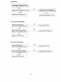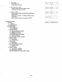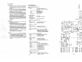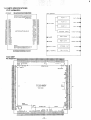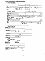
1
Facsimile Transceiver
SERVICE MANUAL
I
I FILE NO.
SFX-30
PRODUCT CODE NO.
1 145 65325
GERMANY
-—
MAIN
SPECIFICATIONS
Type
Desk-toptype transceiver
Line connected
Publlc switchedtelephone network
Size of recording paper
216mm(6.5)
x
30m (98’)/25m (82’)
II
Effectivescanning width
208mrm(8.2”)
Effectiverecordingwidth
212mm(8.3)
I Transmissionspeed
II 9600/7200/4800/2400BPS
I
I Transmissiontime
II Approx. 15 sec. (Transmissionmode: standard)
I
II
Standard: 8 pels
Main scanning density
Fine mode: 8 pals
Sub scanning density
3.85 lines/mm (Standard mode) 7.7 lines/mm (Fine mode)
15.4lines/mm (Super fine mode)
MH (Modified Huffman) and Sanyo original
Compressionmode
I
!,
Reading method
CIS (Contact image sensor)
II
Recordingmethod
I Powersupply
Thermal printing
1,
II AC230V, 50/601-lz
Powerconsumption
Stand-by:
5W,Transmission:
15W,Reception150W,Copy:160W
Overall dimensions
381(W)x 90(H)x 263(D) mm
15”(W) x 3.5”(H) x 1o.4’’(D)
Weight
Approx. 4.3 kg (9.5 lb)
Ambient temperature
5°C - 35°C (41°F - 95°F)
* High-gradethermal paper is 25m (82’).
REFERENCE
NO. SM
620011
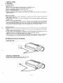
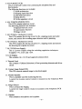
1. INSTALLATION
(1) Unpacking
-
To unpack the SFX-30:
1. Open the carton.
2. Remove the accessories (handset, recording paper roll, etc.) from the carton.
3. Remove the fax machine along with the foam braces on both sides.
4. Remove the polyethylene wrapping around the fax machine.
5. Remove the transportation tapes.
6. Save the carton and the foam braces for later storage and/or shipping.
7. Place the machine where there is access to an AC outlet and a modular phone jack. (Be sure to observe the
precautions below.)
Placement precaution
● Avoid placing the SFX-30 in humid or dusty
places, or in places where it will be exposed to excessive heat
(direct sunlight, heaters, etc.).
● Do not step on or set anything on the AC cord. DAMAGE TO THE AC CORD IS A SAFETY RISK AND CAN
cAusE A FIRE.
. Install the unit only on a stable surface.
. Do not connect the SFX-30 to the same AC outlet as appliances that generate large amounts of interference
(heaters with thermostats, appliances with motors, etc.). It is best to use a completely separate electrical outlet.
● Keep the SFX-3Oaway from water. If water accidentally enters the unit, unplug the AC power cord ‘immediately.
DO NOT SWITCH THE UNIT ON AGAIN. Contact an authorized Sanyo service center or dealer.
b
Handling precaution
. Do not remove any parts that are held in place with screws. (The SFX-30 does not contain any user-serviceable
items).
. Maintain standard room temperature 5°C – 35°C (41°F – 95”F) during use. Do not subject the unit to shock or
vibration. Do not move the unit while it is in use.
● A rapid increase in room temperature in cool weather can cause condensation to form inside the unit. If this
happens, wait at least 15 minutes after turning the unit on before attempting to operate it.
Failure to do so may result in paper jams and/or poor print quality.
● When cleaning the cover or operation panel of the unit, wipe gently using a damp cloth to which a small amount
of a neutral detergent has been added. NEVER USE SOLVENTS OR CHEMICALLY TREATED CLOTHS.
(2) Telephone line and AC connections
~Connecting to AC
I Connecting to telephone line
●
The SFX-30 should not share a modular jack with other communication
equ!pment, as this may obstruct the proper tunctloningof the umt.
L
—1 —
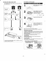
(4) Installing recording paper
(3) Setting the dialing mode switch
Set the dialing mode switch (DIAL) to the correct position for
your telephone line.
Open the pr~~e:t!vecover and rear cover.
press the LOPENfl button to open the
recording
1
telephone
Push-button
telephone
/
=
‘1
A
paper cover
_J
Rotary-dialing
telephone
-.
Place
2
the
supplied roll, in the dlrectmn
shown in lhe diagram, m the paper holder
with both sides sested securely
● Remove
any slack from the roll
Insert the”end
of the roll Into the record-
sounds
Sr
Correct
Wrong
...
,,,
/-----<.
----e
ing paper exit slot
,“”
L
-
....
---. —------...——.
..C2.!ES
Pull out the end of the roll from the record-
“.
ing paper exit untd It extends
.-==;.–..
..
L>.
4 Inches
‘r
‘-“
L-------------------
.-. _-- ——-—
—----- ——..
Close the recording paper cover by
pressing both left and right corners of
the far end of the cover firmly
The SFX-30 cuts the extra recording
paper automahcally.
——.
\
Set the
10
switch
PULSETONE
L ___________________
PULSETONE
)@
■
■
. . . . . . ..-——. . . . .
Use only the recording paper specified for the SFX-30.
The rear cover must be left open while the SFX-30 is in standby mode.
High-grade thermal paper
SFX-30 is compatible with the high-grade thermal paper, a new type fax
recording paper with plain-paper qualify. Unlike regular thermal paper, the
h!gh-grade thermal paper does not fade with time, can be written on with
pencil and can be erased.
The
SANYO Type 6326731727,216
mm (8.5”) wide and 25 m (82) long.
A 12-reeler (39’) long roll is supplied with your SFX-30.
Thermal paper
SANYO Type 6323250047,216
mm (8.5) wide and 30 m (96’) long.
To purchase, contact your dealer.
d
Anti-curl system
SFX-30
has a built-in anti-curl
eystam that prevents thermal recordhtg
paper (high-grade or regular) from curling.
The
‘ you are not sure which dialing system your telephone is using,
ontact your telephone company.
~hen
Setting the A4 Recording Paper
1. Removethe recordingpaper guide
Push me guide to ~ direction snd lift I!
to Q as shown in the figure
2.
Replace the recordingpaper guide
in A4 position
Push the guide to 8 and then to Q
direction 8s shown In me figure
‘u
—2—
(5) MACHINE INITIAL
1. Connect AC plug into AC outlet.
Jun
-
2. Press ~MENu key while ‘SET] key is being pressed and
keep this condition at least one second.
.26
’93
INITIAL
12:00
SET
?
3. Press :SETl .
ALL
4. Press SETI or IMENU
FSE~ :“Clear all items then return to STAND-BY display.
At the same time S-RAM check is also carried out.
ml:
Individual items.
5. Press ~
or -~
.26
’93
RAM
CODE
O.T
&
12:00
CLEAR
?
S.D
CLEAR?
.
: Clear one-touch and speed dial memory and goes
to the next item.
m]:
REPORT
DATA
Jun
’93
CLR?
Just goes to the next item.
7. Press ~
[S=
Jun
: Just goes to the next item.
6. Press ~
H
?
or IMENU]
~S—~ : Initialize RAM CODE and goes to the next item.
~M=]
CLEAR
.
or ‘m
,
.26
12:00
: Clear Activity report data and return to STAND-BY
display.
ml:
Just return to STAND-BY display.
REMARKS
In case of S-RAM Error at step 4, alarm sounds continuously
+
and the machine goes into “DEAD LOCK’ condition
Repairing is required.
IS RAM
CHECK
ERROR
I
(6) MACHINE PROGRAMMING
<SETTING YOUR STATION NAME AND FAX NUMBER>
1. Press -]
2. Press ~
L
5 times.
SET
MODE
?
O.T
DIAL
SET
.
3. Press lml
?
twice.
STATION
CODE
SET
4. Press ~.
I
5. Enter your station name.
A maximum of 24 characters can be entered.
(See page 4)
6 Press ~
ABCDE~
.
7, Enter your fax number.
Your fax number can be entered up to 20 digits in length.
Example 0123456
8. Press ~
012345M
.
Jun
9. Print an activity report (see page 34) to make sure that your
station name and fax number have been cwogrammed
correctly.
—3—
.26
’93
12:00
■ To print programming,
I
press
If you make a mistake
~O~C]
in entering
.
a character,
..— —
press LSTOP/C]
■ To enter a hyphen (-) between two digits, press ~PEED
■ To enter a plus sign (+) preceding
,
The header
can be printed
your fax number,
either outside
the original
and then re-enter
the letter or number.
DIAL].
press ~OL~
document
.
(in the top margin)
can select the desired
setting using feature switch No. 20. Default setting is printing
NOTE If you choose to print the header inside the document, the top of the original
or inside the document
itself. You
outside of the original.
document (about 1 cmjO.4”)
may
not be reproduced.
Printing outside of the original.
SANYO
——
——
— Jun. —26— —’9312:00
l–
I
I
I
012345
P.1
—.—- ———— ———- FAX
-—-—
--—— ———- ———. -——-T
Printing inside of the original.
,––––-–
I
I
I
–--–:.–
_____
----------------
–––--–––––
-––____________T
P.1
FAX 012345
SANYO
Jun. 26 “93 12:00
–--___
;
I
Entering names
Before
programming
keys. Each alphabetical
I
the one-touch
ancf Speed-cfial memory,
you need
to know how to enter names
using number
letter and Symbol are assigned to a p-digit code as shown on the next page.
Entering letters
Example: To enter SFX
1. Press ~
. @ to enter S.
2. Press ~
“~
to enter F.
3. Press 12J “ ~
to enter X.
4. Press
1
O . ~
E!
S9
I
1
SFXl
to enter space.
SFX
9
1
SFX
6H
1
SFX
67~
I Entering numbers
Example: To enter 67
1. Press
El
6 to enter 6 and then press
to move
2. Press
the cursor
7 to enter
El
—
[1 key
#
—
to the right.
7.
4—
I
w
-mm
-m.
.
.
-
lalxe ot letter and symbol codes
Character
Code No.
Character
space .. ........ 00
.. .........01
●
●
Code No.
Character
Code No.
Character
Code Nc
m .... ...............56
........ ............ 14
K ................... 28
‘f ................... 42
........ ............ 15
L ....... ............ 29
z ..... .............. 43
~ ...................57
0 .... ..... ..........58
16
M ......... . ... ... . . . 30
a .... ...... ... .... .. 44
.. .. .. .. ...03
17
N ... ... ... .. ..... ...31
b . ... .. ...... .... . .. 45
p . ..... ...... .......59
,
.. .. .. .. ...04
A ................. ..
18
0 ................. .. 32
C ................. .. 46
q ...................60
+
........ ...05
..........06
B ................. ... 19
c ................. .. 20
P ................... 33
Q ................. .. 34
d ................... 47
e ................... 48
s ...................62
t
........ ...02
r
...................63
.........07
D . ................. .. 21
R . . ... .... .. .... ... . 35
f
...........08
E . ................. .. 22
S .................. . 36
g ................. .. 50
&
*
..........09
...........10
F . ... ..... ....... .. .
23
T . ................. . 37
h ................... 51
v . ..................65
G . ................. .. 24
u... ... .... .... .....
38
i
...... ..... ...... ..
WI . ..... ..... ........66
#
!
... ... .....11
H . .. ...... ....... .. .. 25
v . ....... ... ... .... . 39
j
.. ...... ...... ... . . 53
... .. ... ...12
I
. . . . . . . . ...13
J . ................. .. 27
w . ................. . 40
x . ................. . 41
k ................... 54
I ................. .. 55
. . ... ......... .... . . 26
To enter number:
—
and press ~
O—6
. ................. ............
Enter the number
7—9
...... ................. ........
Enter the number. The cursor
If you make a mistake
in entering
1. Press ~NUl
5 times.
3. Press ~
again.
❑
# to move
El
. . . . . . . . . . . . . . . . ...68
* to move
El
right or
SET
MODE
?
O.T
DIAL
SET
key 2,
.
left to
O.T
No.
.fl?
O.T
No.
.5?
?
B
6. Enter the party’s name (to a maximum of 16 characters).
(See page 4 for detailed instructions)
7. Press ~
lABCDEm
I
II
8. Enter the fax (or telephone) number.
(A maximum of 32 digits can be entered including
and hyphens.)
Example 0123456
9. Press ~
y
Z ...................69
1
4. Press one-touch dialing key (1-8).
Example To program a number in the one-touch
.
press one-touch key
5. Press ~
)( . ..... ... ...... ... . 67
and re-enter.
DIAL MEMORY PROGRAMMING>
.
52
to move corsor right.
a letter or a number, simply press
<ONE-TOUCH
2. Press ~
“ . ..................64
moves to the right autornatiCally.
space and then enter the correct letter or number.
. To clear a name or a number, press -]
................. .. 49
...................61
I
the appropriate
<.
Character
;
. ...................
> ................
,
u
Code No.
I
I
pauses
012345~
.
To program other one-touch
keys, repeat steps 4-9 above.
—5—
10.
TNo.
=B?l
10. Press FS~]
to finish one-touch
number program-
Jun
.26
’93
12:00
ming.
● For instructions
■ To interrupt
on printing
programming,
out a numerical
list of programmed
press -]
names and numbers,
see page 4.
.
■ To enter a hyphen (-), press m~.
■ To enter a three-second
semicolon
(;) indicates
<SPEED-DIAL
pause between
two digits of a number,
press
[REDIALiPAUS~
in the appropriate
place. A
a pause.
MEMORY PROGRAMMING>
1. Press ml
5 times.
2. Press ~
.
3. Press m]
.
4. Press ~
SET
MODE
?
O.T
DIAL
SET
SPEED
.
5. Enter a speed-dial number using the number keys.
Example To store a fax number in the speed-dial
.
number 10, press ~, then
DIAL
?
SET
SD
No.
.Ou?
SD
No.
=l~?
?
❑
6. Press ~
7. Enter the party’s name (to a maximum
characters).
(See page 4 for detailed instructions.)
8. Press ~
of 16
ABCDE~
.
I
9. Enter the fax (telephone) number to be stored.
A maximum of 32 digits can be entered, including
pauses and hyphens.
Example 0123456
I
012345~\
.
10. Press ~
Repeat steps 5-10 to program other numbers.
11. Press -1
programming.
to
finish
speed-dial
S.D
number
Jun
No.
.26
=Ifl?
’93
12:00
“G
■ For instructions on printing out a list of programmed names and numbers, see page 4.
■ To interrupt programming, press [-]
.
■ To enter a hyphen (-), press ~\.
B To enter three-second pause between two digits of a number, press IREDIAL/PAUSE
semicolon (;) indicates a pause.
—.—
I in the appropriate
.—
.—.
LCanceiing programmed
one-touch dialing numbers
—
1. Press -]
2, Press [=E~]
place. A
j
five times.
twice.
Example:
3. Press the one-touch
to cancel.
One-touch
2
dialing key of the number you want
0.1
—6—
No.
.g7
w
4. Press Lf3ET ].
w
EEALER
A
I
5. Press [STOP/C’],
6. Press [~.
——.
Repeat steps 3 – 6 to cancel other one-touch
7. Press [STO~
———
I
key.
O.T
No.
to finish canceling.
~carice~w
programmedwed-dialing
numbers
_
———
1. Press ~NU
IQ?J
=
_“.__
’-
] five times.
2. Press ~ETl
3. Press [MENU;.
L
4. Press [S~l.
Example:
5. Press the number
Speed-dial
to be canceled.
I
6. Press [~].
number 10
S. DNo.
=l~?l
IEEALER
A
I
7. Press @TOP/Cl.
8. Press\ SET\.
Repeat steps 5 – 8 to cancel other speed-dial
numbers.
9. Press -].
<CALENDAR AND CLOCIO
L
1. Press ml
5 times.
2. Press ~
3. Press -]
4. Press ~
3 times.
O.T
DIAL
SET
SET
?
?
.
H If you make a mistake, move the cursor to the appropriate
❑ to move the cursor
❑ to move the cursor
N4.
10
’93
10:00
~6.
26
’93
12:00
.26
’93
12:00
‘“
r
Press
?
.
Emlmmmmmmml.
Press
MODE
TIME
5. Enter the month, day, year and time using the number
keys.
●
The time must be entered using 24-hour system.
. The month, day and year should be entered in 2
digits each.
Example to enter June 26, 1993, 12:00, Dress ~.
6. Press ~
SET
right.
left.
—7—
Jun
place, then enter the correct number.
I
2. PERIODICAL
INSPECTION
AND MAINTENANCE
I
I
—1
ml
C9
N
C9
—8—
3. OUTLINE
(1) Pad name and functions
Front view
~u~on
hpen
Original guide
I
]
I
-Cove’
guide
Original
Right side
_._———
.———..—--.-——
___.——
PULSE TONE
AUTO MANU
F!
slot
-.
---
.!.7
I
AUTO/MANU
switch
PULSE/TONE
switch
~
Handset jack
, Handset
Rear view
/“”
Rear ;over
\
/
AC
Inner view
Telephone line jack (LINE)
cord
f
)
F!&4
~
p
“--mlF’=’FsOr
ment release lever
ment feed roller
L Green releaselever
—9—
:fNTsUl
(
1
%3
[
1
L=
ERROR Lamp
@ (FEHLER)
_
I
‘o’i’cp’
STOP/L
@ One-Touch Keya
I
KOPIE
p,
I
80
I
‘c
Shows calendar and clock functions, operation guidance, machine status, e
●
Frequently dialed numbers can be stored in memory using thesa 8 keys
The one-touch keys are also used when entering names in memory.
●
Llghta if a communication error occurs.
Press this key when selecting verioua functions.
● SETKey
●
Preee thla key to confirm aela%ona.
●
Preee this key to set to answer mode.
●
Lights when the unit ia set to answer mode.
r
These keys are used to dial fax and phone numbers and to change various
functions.
TONE Key(•)
●
Press this key to switch
@
HOLD
● Tem&rarily
@
SPEAKER Key(~)
Number
~
Keys O-9
Key(@)
—
e
●
places
pulse
dlalmg
to Touch-Tone
0
dialing.
a call on hold.
—
Allows you to momtor a call without using the handset.
●
Press this key to select contrast settings.
●
Press this key to select resolution setlmgs.
—
●
Press
COPY Key
●
Press to make a copy.
sToP/c Key
. Press to interrupt transmission/reception/copymg or to atop the ERROR
indicator Iightmg.
● Press to cancel various setting and dialing funcflons and to remove an
original document that has been placed in the unit.
—
RESOLUTION Key
(AUFLOSUNG)
Press this key when using speed dial.
. Press this key to radal the last number dmled.
Press this key to insert a peuaebetween two d~ife in a number Eeing dialt
●
—.
from
●
@ START Key
LSmfI
#“
.
~
ANSWER Key
e
7“●
@
@f CONTRAET Key
L-I 0AN5wER
‘o
●
●
L--
FEHLSF4
START
\ @ MENU Key
~
I
to start
transmission
or manual
reception.
‘-
(3) Original documents precautions
9 Transmittable
original
■ Effective text width
size
~208
148 mm
(5.8”)
I
Maximum
T
1.5 m
(4.9’)
1
●
I
I
mm(8.2’’)pl
1
Minimum
148 mm
/’4
/’.
/,
/,
0
Insertion
direction
J
J
direction
Note:
/,
An original other than specified should be reduced
or enlarged by the photo copier then the copy can
be used as an original document.
■ Effective thickness
I
I
[
I
I
thickness
(per sheet)
1 original
sheet
multi sheets
~
-—
0.05–0,15 mm
(0.002” - 0.006”)
0.08– 0.13 mm’~
(0.003” - 0.005”) J
—11—
direction
H
A
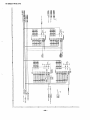
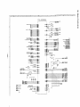
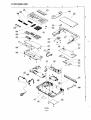
4. MECHANICAL
OUTLINE
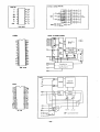
O. Transmission Mechanism
When, in Fig. 4-1, the document is inserted, the first sensor detects the
document and the transmission motor starts to rotate.
Subsequently, the automatic document feed roller also rotates and
the document is fed to the position of the platen roller and is stopped.
(the automatic document feed roller also works for the separation of the
document when multiple documents are inserted)
When the START or COPY button is pressed here, the transmission motor
rotates again and the document is fed forward.
@. Reception Mechanism
As shown in Fig. 4-1, the recording paper is pressed by the platen roller and
the thermal head. The platen roller is rotated by the reception motor and
feeds the recording paper forward. When the printing is finished, the
recording paper is fed to the cutter until its cutting position and it’s cut.
—
There are two sensors for the recording paper, one is for detecting the
recording paper itself and the other is for detecting its jamming.
It is noted that it will be a cause of recording paper jam when the recording
paper is not inserted straight or is not rolled tightly.
Original document paaa
Jam Sensor\
R
—
or
M4 (Tel
Receiving Motor
M3 (NCU) PCB
Fig. 4-1
—12—
Ml (main) PCB
(CIS)
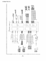
3, M-3 PCB(NCU PCB)
This is a Network Control Unit connecting the telephone line and
this facsimile.
The following fimctions are included.
O Hookup detection
@ Ringing signal detection
@ Dial pulse generation
@ Relay drivers
@ Tx/Rx separation circuit
4. M-4 PCB(TELEPHONE PCB)
This PCB contains telephone circuit.
The following fh.nctions are included.
0 Speech Network circuit
@ Line monitor function
9 Ringer circuit
5.
M-5 PCB(RX. Mechanism Control)
This PCB contains the driving circuit for Rx. stepping motor and cutter
motor, and sensors for recording paper detection and its jamming.
6. M-6 PCB(TX. Mechanism Control)
This PCB contains the driving circuit for Tx. stepping motor and sensors
for detecting the original document.
7. M-7 PCB(Power Supply)
This is a power Supply using the switching regulation techniques.
It supplies +5V, *12V, and +24V.
8. LCD Display
This contains 16x 1 LCD and segment/common driver.
9. Thermal Head
This contains 1728dots (8dotshnm) of heat generating elements and driver
circuit.
10. Contact Image Sensor(CIS).
This CIS converts scanned image to electrical signal.
11. Monitor Speaker.
This is a speaker used for monitoring the line.
A switch for monitor control volume is mounted on the Telephone PCB
(MA).
12. Ringer Buzzer
This is a buzzer for ringing.
A switch for ringer control volume is mounted on the Telephone PCB
(M4).
13. Handset
This contains
a
microphone and a speaker.
—14—
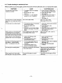
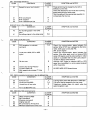
5-2. Trouble shooting for mechanical
When trouble occurs, thoroughly
SYMPTOMS
Parts
confirm the cause of the trouble and carry out appropriate repair.
CAUSE
COUNTERMEASURE
The document, even when
inserted, is not fed.
1. The platen roller is not rotating
properly.
2. Dirt on the ADF roller.
(roller 1)
3. The sensor 1 is not adjusted
properly or out of operation.
1. Press the green release lever,
then insert the document again.
2. Clean the ADF roller.
(See page 8)
3. Adjust the level of the sensor 1.
Confirm the operation of the
sensor 1.
(See page 12)
The documents are fed overlapping.
(More than one sheet are fed at a
time.)
Dirt on the rubber sheet.
Clean the rubber sheet.
(See page 24 Fig. 6-16)
The document
1. The original guide is not adjusted
along by the original.
2. Dirt on the platen roller.
(roller 2)
3. Pressure for the Contact Image
Sensor is not equal in the both
sides.
1. Adjust the original guide along by
the original.
2, Clean the platen roller.
(See page 8)
3. Adjust the pressure repositioning
the Contact Image Sensor.
(See page 23)
When copying or transmitting the
exceeding part of the original is
printed as blurred black if less than
A4 or letter size of original is used.
The exceeding part of the original
on the platen roller is dirty.
Clean the platen roller. (roller 2)
(See page 8)
When copying, white vertical line
appears that is not on the original,
1. There is dirt sticking to the
thermal head,
2. The heating element of the
thermal head is broken.
1, Clean the thermal head.
(See page 24)
2. Replace the thermal head.
(See page 24)
Although the recording paper is in
the position, “CHECK PAPER
ROLL” is indicated on the LCD.
1. The recording paper
not adjusted properly
operation.
2. The recording paper
placed in the proper
1. Adjust the level of the 1st Sensor.
(See page 12)
2. Place the recording paper
properly.
is not fed straight.
sensor is
or out of
is not
position.
No cutting the recording paper.
The copy cut previously still remains
in the cutter position.
Remove the copy remained in the
cutter position, then confirm the
performance. (Still same situation,
Replace the cutter.)
(See page 24)
When copying with High grade
thermal paper, the copy is shrank.
The recording paper is placed
slackly.
Place the recording paper without
slackness.
—15—
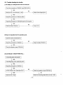
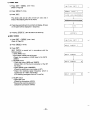
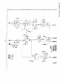
5-3. Trouble shooting for circuitry
(1) No displayon LCD light when Power is turned ON.
Check the connection
of CN6 (M-1) and CN61 (M-6).
Check pin No. 12 of CN7 (M-1), +5V?
Check the connection
1
1
of CN2 and CN21.
YES
Check the connection
I
Check Power Supply (M-7).
of CN22 (M-2) and L~l
YES
Check the Main PCB (M-1)
(2) Key-in is impossible from the operation panel.
Check the same as described (1).
YES
/
Check the connection
of CN2 (M-l).
Check the Main PCB (M-l).
L
T
I
Check the operation panel PCB (M-2).
.—
(3) LCD indicates“CHECK PAPER ROLL”.
EIIs=L
Is recording paper set properly?
In the Receiving cover closed securely?
~
Check the connection
I
of CN5 (M-l).
YES
is/PAP (CN5-pin No. 4) less than 0.5V?
I
&
Check the reception mecha PCB (M-5.)
I
L
I
1
1
NO
Check the recording paper SW on the M-5 PCB.
—16—
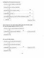
(4) No motor rotates when the original is inserted.
NO
Check the connection
1s/S1 (CN6, pin No. 14) low?
of CN6 (M-l).
A
<-””
YES
1
NO
Check the connection
I
.—
Check the S1 sensor.
CN6 (M-1) and CN61 (M-6.)
YES
NO
Check the M-1 PCB.
ls/TMIO-3 (CN6, pin No. 20-23) OK?
J YES
Check the connection
i
of CN62.
YES
Check the Transmission
I
Mecha control PCB (M-5).
YES
Check the Transmission
\
I
motor.
I
(5) No copy is made.
NO
I
r
Is the Head test OK? (See page 27)
1
YES
1
Check the printing circuit.
1
1
t
Check the reading circuit.
(a) Printing Circuit (To be confirmed by the Head test)
%_
Check the connection
1
of CN4 (M-1 ) and CNTPH (Thermal head).
YES
Check the power supply PCB (M-7).
Does +24V appear at CN7, pin No. 15?
I
YES
NO
Does HVON (CN7, pin No. 1) work properly (High at printing)?
I
YES
NO
Do the signals (DATA (CN4, pin No. 6), CLK (CN4, pin No. 7)) appear normally?
I
1
YES
Do the signals (/STBl,
/STB2 (CN4, pin No. 8, 9)) appear normally?
I
L
YES
1
1
I Check the Thermal head. I
Check the M-1 PCB.
—17–
(b) Reading Circuit (To be checked by Scanning test)
Check the connection
of CN6 (M-1) and CN61 (M-6).
I OK
Check the connection
of CN63 and CNCIS (CIS).
YES
Does VIDEO (CN6, pin No. 10) appear normally?
1
YES
NO
Is GLED (CN6, pin No. 2) low?
I
YES
Do the signals (S1(CN6, pin No. 5) and CLK (CN6, pin No. 3)) appear normally?
I
YES
Check CIS.
F
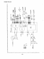
(6) Can not enter the TxJRx. mode by pressing @TART] switch under OFF-HOOK condition
(a) In case of the extension telephone connected to the SFX-30
Check the connection
I
of extension telephone and MJ42 (M-4).
YES
Check the NCU (M-3).
ls/HS (CN31, pin No. 8) low on the NCU PCB (M-3)?
YES
/
Check the M-1 PCB.
(b) In case of the Built-in telephone
Check the connection
I
OK
Check the connection
I
of CN31 (M-3) and CN3 (M-l).
of MJ43 (M-4) and handset.
I
OK
NO
I
I
Check the M-4 PCB.
ls/DHS (CN41, pin No. 7 on M-4) low?
&
—18—
(7) No Dial out
Is the position of the Dial selection
switch (SW2 (DP/ PB)) on M-1 PCB?
I
I
1
I
OK
t
Which can not be dialed, DP or Tone?
I
1
I
Check the Tone related clrcut
*=
Is the position of the DP selection
memorv. switch (1O/20PPS) correct?
Check the DP generation circuit.
(a) In case of the TONE dialing
NG
Does the TXLINE (CN3, pin
No. 17 on M-1) appear normally?
I
Check the M-1 PCB.
OK
NG
Do the TEL1 and TEL2 (CN33,
pin No. 7 and 8) appear normally?
Check the NCU PCB (M-3).
1 OK
I Check the TEL PCB (M-4).
I
(b) in case of the DP dialing
NG
Does the DP (CN31, pin
No. 11 on M-3) appear normally?
1
Check the M-1 PCB.
OK
NG
Do the TEL1 and TEL? (CN33,
pin No. 7 and 8) appear normally?
Check the NCU PCB (M-3).
I OK
I Check the TEL PCB (M-4).
—19—
I
(8) Power supply check (M7)
—
@
-r-
I
t
I
k3Z“l
short?
I
-
Yee
1-
I
—
iI
‘s;:p~lNO j ‘R’:? p
~
z
Is IC703, 704
short?
tS IC702 short?
‘0
No
@
5-4. Error code list
EIO, E121
CODE
Check other fault
condition
Yes
‘es
> other party does not respond
CONTENTS
10
T1 time over
12
No response on redial
CLASSIFICATION
I
T, R
T, P-T
I
SYMPTOM
and NOTES
Even 35 +/- 5 seconds passed after starting communication, no signal received from the party.
No response from the party even redialing of the
timer transmission is carried out.
-
~20 - E27 ( vn machine troubles
CODE
CONTENTS
20
Stop switch is ON
21
23
26
27
Original jam
No recording paper
No original for timer transmission
Timer oc)eration is cancelled
I CLASSIFICATION
ALL
T
R
T
TIMER
—20—
!
I
SYMPTOM
Transmission
[STOP] key.
and NOTES
is stopped caused by pressing the
Timer is cancelled
by manual operation.
SYMPTOM
CLASSIFICATION
~
31
32
33
Exceed the error line limitation
R
RTN transmission
RTN reception
Over 5 seconds per line
R
T
R
E40, E41 Error in the other party
CONTENTS
CODE
40
41
k-
350- E59 (
These errors may be caused by the S/N or
deflection on the line.
Check the disturbance and verify the incoming
signal level using the level meter.
Test the setting of the appropriate equalizer to
compensate the line loss.
I
and NOTES
SYMPTOM
and NOTES
P-R
t-off other party
CLASSIFICATION
CONTENTS
T, R
DCN reception or unknown
Check the communication
status between the
parties. When STOP key is pressed by the transmitter, DCN signal comes after PIX.
(PIX: picture signal)
Check the communication
status between the
parties. If the other party could not receive DCS
signal, DIS signal would be retransmitted. In other
cases, it is possible that the other party disconnected the line by some reasons.
Although MCF signal to respond MPS or CFR
signal was transmitted, no carrier signal received
within 6 seconds.
command
51
SYMPTOM
T
No recording paper in the other
party
No polling original in the other party
CODE
50
I CLASSIFICATION
and NOTES
Triple
T
trial of DCS, DTC or NSS
signal
52
T6 time over
R
53
54
59
Carrier drop during Phase C
Q, PRI-Q triple trial
Multi page(mode change) T1 time
R
T
T
Q: EOP, MPS, EOP General terms
over
“i
E60 - E62 I
CODE
:omplete transmissions
due to deficient line.
CONTENTS
60
62
71
Fall-down Out
Continuous 300 BPS
Unhatching of key code
77
40 ms of 9600
BPS only
E80 - E85 DCS, NSS command
CODE
80
81
82
83
85
I CLASSIFICATION
I
T
and NOTES
Training failure even with fall-down to 2400 bps.
This error may be caused by the line noise.
Telephone number does not match when the
select reception is set.
T
T, R
R
I
SYMPTOM
I
error
CONTENTS
CLASSIFICATION
R
R
Other company’s NSS
No R command
(Receive command)
Original size A3
B4 command for A4 machine
Minimum transmission timer error
R
R
R
—21 —
SYMPTOM
I
and NOTES
!
6. REPAIRS
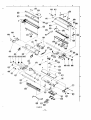
6-1. Removal of the main parts
(1) Removal of the cabinet
a) Turn over the machine and remove three screws
securing the cabinet. (See figure 6-1 )
b) Open the original tray and the operation panel,
then remove three screws securing the cabinet
(See figure 6-2)
c) Press the open button to open the receiving cover,
then remove the cabinet. (See figure 6-2)
d) Disconnect the CN 43 on the M-4 (TEL) PCB.
(See figure 6-3)
d) Disconnect the connectors CN2 and CN6 on the
main PCB (M-1) while lifting up the transmission
mechanical unit. (See figure 6-5)
(3) Removal of the receiving mechanical unit.
a) Remove the cabinet. (Refer to the procedure
6-l-(l))
b) Remove the transmission mechanical unit.
(Refer to the procedure 6-1-(2))
c) Remove two screws securing the receiving
mechanical unit. (See figure 6-4)
m
\\
two screws securing receiving mechanical unit
three screws securing the cabinet
M-1 (main)
PCB
.GURE 6-4
M-3 (NCU)PCB
L
FIGURE 6-1
\
/
//
d) Disconnect the connector
CN5 and CN7 on the
main PCB (M-l). (See figure 6-5)
IJ
two screws
securing the bottom cover
open button
—
\(
\\
original tray
(4) Removal of the main PCB (M-1).
a) Remove the cabinet and the transmission
I
mechanical unit. (Refer to the procedure 6-1-(1)
and 6-1 -(2))
b) Disconnect the connectors CN4, CN5 and CN7 on
three screws securing
the main PCB (M-l). (See figure 6-5)
c) Remove two screws securing the main PCB (M-l).
(See figure 6-5)
d) Remove the main PCB (M-1) while pressing down
M-3 (NCU). M-3 and M-1 are directly connected
through the connector.
-
F-JL=JOperatiOnpane’
“:::
(2) Removal
of the transmission
mechanical
unit.
a) Remove two screws securing the bottom cover.
(See figure 6-1)
b) Remove the cabinet (Refer to the procedure
6-l-(l))
c) Remove two screws securing transmission
mechanical
unit. (See figure
CN2
M-4 (lE
M-~(main)
6-3)
one
E 6-5
(5) Removal of the M-3 (NCU) PCB.
a) Remove the cabinet and the transmission
mechanical
unit. (Refer to the procedure
M-4
6-1-(1)
and 6-1 -(2))
b) Remove the main PCB (M-1). (Refer to the
procedure
6-1 -(4))
c) Remove
one screw
securing
the M-3 (NCU).
(See figure 6-5)
F
—22—
d) Disconnect the connectors
(See figure 6-5)
CN41 and CN42.
-
L
(6) Removal of the M-7 (Power Supply) PCB.
a) Remove the cabinet, transmission mechanical unit
and receiving mechanical unit. (Refer to the
procedure 6-1 -(l), 6-1 -(2) and 6-1 -(3))
b) Disconnect the connectors CN71 and CN73. (See
figure 6-5)
c) Remove the M-4 (TEL)PCB and one screw for
earth wire coming from the M-7 (Power Supply)
PCB. (See figure 6-5)
(7) Removal
(9) Removal of M-5 (Rx. Mechanical Control) PCB.
a) Remove the receiving mechanical unit. (Refer to
the 6-1 -(3))
b) Remove two screws securing the M-5 (Rx.
mechanical control) PCB. (See figure 6-8)
-\CN52 CN54
CN53II-LA&-L
.4
of M-4 (TEL) PCB.
a) Remove
the cabinet.
(Refer to the procedure
6-1M-5 (Rx.mechanical control) PCB
(1))
b) Disconnect the connectors CN41 and CN42 on the
M-4 (TEL) PCB. (See figure 6-5)
c) Remove one screw securing the M-4 (TEL) PCB.
(See figure 6-5)
L
(8) Removal of M-2 (Operation Panel) PCB and LCD.
a) Remove the cabinet and Transmission mechanical
unit. (Refer to the procedure 6-1-(1) and 6-1-(2))
b) Remove two screws securing the M-2 (Operation
Panel) PCB. (See figure 6-6)
c) Remove five screws securing the reverse side
cover. (See figure 6-6)
d) Disconnect the connector CN22 on M-2 (Operation
Panel) PCB. (See figure 6-7)
e) Remove eleven screws securing the M-2
(Operation Panel) PCB. (See figure 6-7)
9 Remove LCD by removing two screws. (See figure
6-7)
f-’
two screws securing the M-5
(Rx.mechanical control) PCB
~eceivingmechanical unit
FIGURE 6-8
c) Disconnect the connectors
CN54. (See figure 6-8)
CN51, CN52, CN53 and
(10) Removal of M-6 (Tx. Mechanical Control) PCB.
a) Remove the transmission mechanical unit. (Refer to
the 6-1 -(2))
b) Remove the hooks (two places) fixing the M-6 (lx.
mechanical control) PCB. (See figure 6-9)
M-6 (lx. mechanical control) PCB
CN63
five screws securincithe reverse side cover
Transmission
me~hanical
ufiit
I
~
hooks (two places)
I
t+
FIGURE 6-9
c) Disconnect the connectors
(See figure 6-9)
o
n
\
d
\
CN61, CN62 and CN63.
I
/&
.
6-2. Replacement of the main parts
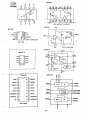
two screws securing the M-2 (operation panel) PCB
(1) Replacement of the Contact Image Sensor (CIS).
a) Remove the transmission mechanical unit. (Refer to
the 6-1 -(2))
b) Remove the operation panel. (Refer to the 6-1-(8))
c) Remove the platen sensor. (See figure 6-10, 6-1 1)
FIGURE 6-6
eleven screws securing the M-2 (operation panel) PCB
platen sensor
pull it out turning the arrow direction
bearing
Q“:” 0
0
m
P
w
two screws s~uring LCD
e“.
*
●
u
FIGURE 6-10
FIGURE 6-7
L
—23—
d) Remove the CIS assembly.
* CIS should
be replaced
(See figure 6-11)
the guide
with CIS assembly.
cutter 1,
1,
2
guide cutter 3
—
two screws securing the guide cutter
connector
3
of the guide cutter
J
FIGURE 6-15
cl
(4) Replacement of the ADF (Automatic
’11
Feeder)
(2)
., Reciacement of the Thermal Head
a) Gather the original guide to the center and remove
two screws securing the receiving cover.
b) Press the Open button and remove two screws
securing the cover located under the thermal head.
(See figure 6-1 2)
c) Disconnect the connector of the thermal head.
d) Remove two screws securing the thermal head.
lfT—————
Document
unit.
a) Open
the operation panel.
b) Remove two screws securing the ADF unit. (See
figure 6-16)
two screws
securing
lk%4EADFuni’
–--—~
~
FIGURE 6-12
two screws securing the thermal head
$
FIGURE 6-16
c) Replace new ADF unit and check the performance.
bracket
bracket f) pressthisdirection
ADF unit
FIGURE 6-13
When attaching the thermal head to the bracket
head, the thermal head should be pressed the
arrow direction. (See figure 6-13)
(3) Replacement of the Auto Cutter
a) Remove the receiving mechanical unit. (Refer to
the 6-1 -(3))
b) Remove one screw securing the cutter unit (See
figure 6-14)
receiving mechanical unit
one screw secu
the guide cutter
utter unit
6-14
c) Disconnect the connector of the cutter unit.
d) Remove three screws securing the black guide
cutter (three pieces) from the cutter unit. (See figure
6-15)
Please note that two wire fixers are fixed together
with screws.
When re-assembling, put them to the same
position.
—24—
6-3. Test Mode
(1) Setting up to the TEST MODE
—
key while ~~
Press ~M~U]
and keep this condition
EACH TEST MODE
key is being pressed
INITIAL
SET
?
at least 1sec.
~
INITIAL
SET
?
‘El
-
Initial Set
‘m
-
Changing
I
Press m
RAM
CODE
SET
?
RAM CODE
I
“scanningTest
~=
Press -1
~m
---
w=
w=
IPANEL
TEST
?
‘MOdemc
“Therms
km
-
ODe-Panel
Check
Press WI
L.
“’;’’’’nost
(2) Explanation of each test modes
a) INITIAL SETTING
+ m).
1) Press ~1
(over 1sec.)
INITIAL
SET
?
(- Refer to Page 6-3-(l).)
2) Press ~
3) Press ~
~
-~
ALL
or w]
–lApr
:Clear all items then return to STAND-BY.
Note) At the same time of this operation, S-RAM
check is also carried out
In case of error, refer to (7).
: Individual item (RAM CODE)
L
—25—
CLEAR
.20
’93
?
12:001
OR
—
RAM
CODE
CLEAR
?
4)
O.T
~
m]:
or -1
:Clear one touch and speed dial memoty
goes to next menu.
w]:
CLEAR?
REPORT
DATA
Apr
’93
CLR?
and
Next menu (Report Data)
6) Press ~
~
S.D
Next menu (One touch and speed dial)
5) Press ~
~
&
:Initialize RAM CODE and goes to next men.
or -1
.20
12:00
:Clear activity report data and return to stand-by
display
-1:
Return to stand-by display
7) In case of S-RAM error
Alarm sounds continuously and the machine goes into
“dead lock” condition. + Repairing is required.
MEMORY
ERR (STOP)
b) RAM CODE SETTING
+ -j
1) Press ~
(Refer to Page 25.)
(over 1sec.)
INITIAL
2) Press ml
3) Press ~
~
IRAM
or ml
:Changethe
m]:
CODE
Sw.
SET
SET
?
?
I
CODE
contents.
Issue RAM CODE LIST and return to STANDBY.
4) Input the SW. No. using numeric or ml
key and
ISW.
01
CODE
Isw.
01
CODE
I
press ~.
5) Input the SET CODE using numeric or ~U\
key and
press ~.
(Next SW. No. is automatically
displayed.)
6) Repeat the steps (4) and (5) on demands.
7) Press -1
to finish.
The SFX-30 returns to STAND-BY.
—26—
03
I
c) SCAN TEST
1) Press ~
+ w]
(Refer to Page 23
2) Press ml
.(over 1sec.)
INITIAL
twice.
SCAN
3) Press ~.
4) Press ~)
SET
TEST
?
?
I
I
I
I
●
*
SCAN
TEST
“
to complete.
A shading signal waveform is memorized then, return to
STAND-BY.
d) MODEM TEST
+ m].
1) Press ~
(Refer to Page 25)
2) Press -1
(over 1sec.)
II
3-times.
* Press ~~
19600BPs
(0)
(1)
(1:1)
(1:4)
(4:1)
:
:
:
:
:
1100HZ
~ pm
-
NO SIGNAL
-
?
(o)
I
1
RETIJRN TO THE 1ST STAGE
(9600BPS)
its carrier frequency
pattern as shown
to change its pattern at each stage.
1850HZ continuously
1650HZ continuously
1650/1850HZ alternately (3.3ms/3.3ms)
1650/1850HZ alternately (3.3ms/l 3.2ms)
I
1650/1850HZ alternately (13.2ms/3.3ms)
* Press ~.
-
* Press -I
4) Press -1
I
to call for the previous signal.
The signals of 9600, 7200, 4800, 2400 and 300BPS can be changed
below.
Press -I
TEST
,
to call for the next signal.
SIGNAL ORDER:
9600 BPS(0) + 7200 BPS(0) + 4800 BPS(0) + 2400BPS(0) - 300BpS(0)
L-+ 2100HZ” -
SET
MODEM
3) Press ~.
* Press ~]
NITIAL
time is a case of 300BPS
MONITOR SPEAKER is activated.
at NO SIGNAL stage. + Voice prompt can be heard.
to finish.
e) HEAD TEST
1) Press ~
+ [-l.
(Refer to Page 25)
2) Press -1
(over 1sec.)
INITIAL
4-times.
HEAD
SET
TEST
?
?
3) Press ~.
A pattern of the head test starts to print on the recording paper. Press -]
to interrupt printing.
After the print has been completed, the machine returns to STAND BY.
—27—
●
*
HEAD
TEST
●
*
f) PANEL TEST
+ FU].
1) Press ~]
(Refer to Page 25)
2) Press ml
(over 1sec.)
INITIAL
5-times.
SET
PANEL
3) Press ~.
II
LCD,
TEST
LED,
?
1
.—
?
BUZZ ERII
The whole LCD and all LED will be turn over, and 2
times of the beeping tone will be heard.
4) Press Keys according to the contents of display. All keys
on the panel will be displayed in sequence.
5) Pressing -1,
SFX-30 returns to stand-by.
I
[STOP]
I
g) SELF CHECK
+ ml.
1) Press ~]
(Refer to Page 25)
2) Press m)
(over 1sec.)
II
6-times.
NIT
IS ELF
sET
IAL
cHEc
K
7
I
7
w
I
3) Press ~.
SELF CHECK is carried out in accordance with the
following order.
1. GATE ARREY 1/0
*R/W check of BUS lines of the port
(Check the connection of BUS lines to the GATE
ARREY)
2. MODEM Check
*Check the cycle of 9600 and 300BPS.
(Check OSC. of XTAL3 and connection of the INT
for clock)
*Check DREQ cycle of 9600BPS.
(Check the switchover circuit relies on INT)
*Check the receiving signal frequency which is
looped back of1100Hz transmitted.
(For checking analogue circuit of Tx and Rx)
3. MUSIP Check
*Check SH cycle
(Check the connection of INT4)
*Execute the scanning operation.
(Check the connection of INTO)
1
T
SELF
CHECK
T
‘“
I
—28—
2
4. RTC Check
*Check
(Check
SELF
INT cycle.
4
CHECK
OSC. of XTAL3)
I
5. MR. Accelerator check.
*Transfer certain data from RLEX to RAM.
(Check the connection of INT3)
6. TPH l/F Check
*Check the pulse width of strobe signal generated on
test purpose.
(Check the operation of STBON, STBINT and the
connection)
*Data Transfer (Check the connection of INT2)
‘.-
“L
IN CASE OF ERROR
(1) DISPIAY
X : TEST No.
XX: ERROR CODE
(2) ERROR CODE
1. GATE ARREY 1/0
01: R/W ERROR
2. MODEM CHECK
01: No clock detection possible
02: 300BPS clock failure
03: 9600BPS clock failure
04: No DREQ detection possible
05: DREQ cycle failure
06: No 1100Hz detection possible
3. MUSIP CHECK
01: Cycle failure
02: Transfer failure
4, RTC CHECK
01: Cycle failure
5. MR ACCELERATOR CHECK
01: No data request
02: Data error
6. TPH l/F CHECK
01: Cycle failure of STBINT
02: Cycle failure of STBON
03: DATA transfer error (No transfer request)
\
—29—
TEST
OK
TEST
X
I
ERROR
XX
..
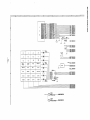
6-4. RAM CODE LIST and its explanation
SW No. 01-57 are opened to the users.
Settingitems
SW No.
01
Pause
time
Setting No.
02
2 sec.
I
I
12 sec.
12
02
Hook-up alarm
00
01
05
06
Contents
Number of radial for
00
Time Tx.
01
02
03
Explanation
Fact. sei
Setting No. x 1 sec. = Pause time to be set
The initial factory-preset of a pause is 3 sec.
OFF
ON
01
This is to set the number
No redial
1 time
of repeat call
attempts when the called paw is busy or no
response.
2 times
03
3 times
(3-4 min. interval between each call.)
Number of redial for
00
No redial
This is to set the number
immediate Tx. using
01
02
03
1 time
attempts when the called parly is busy or no
response.
O.T/SpeedfNum.
key
02
2 times
of repeat call
(2-3 min. interval between each call. This is
3 times
also effective for Polling Rx.)
08
Remote reception
00
01
02
09
16
17
T Dialing
method
of
the
extension
DTMF
J telephone for the remote reception.
- No Tel f Fax switchover
00
No ringing
sounds after the line is
01
02
03
04
05
3 times
Number of rings that sounds before the
5 times
SFX-30 switches from telephone mode to
fax reception mode when a manual fax
Hold melody
Voice announcement
Key operation sound
00
Header print
03
7 times
9 times
11 times
transmission or voice call is received in
1 the AUTO mode.
Silence (No
melody)
telephone line when the conversation
MINUET
on hold.
GREENSLEEVES
00
OFF
01
ON
01
00
OFF
ON
01
sound generates or not
OFF
ON (outside
01
number and date/time
00
01
is put
02
This is to set whether the voice announcement is released or not.
This is to set whether
the key operation
Determines whether your station name, fax
.
are printed on the
‘4
header.
original)
02
w
This is to set the melody released to the
01
02
01
20
- No remote reception
Number of rings that
connected
10
00
OFF
DP
ON (inside
original)
23
Print Density
00
Normal
01
Darker
26
Closed network
communication
(Receiving)
00
01
OFF
checking
telephone
number
27
Transmission mode
00
initial
01
02
03
Standard
Fine
00
Set print density.
00
Determines whether reception
to programmed fax number.
is restricted
Return to the position after Tx. or copy.
T
Super fine
No initial
1
03
- No initial is executed.
‘e
—30—
Settingitems
SW No.
Original contrast initial
28,
00
01
02
03
Transmission report
31
Exrianation
Fact.set
Contents
Setting No.
Normal
Light
Same explanation
planation.
36
previous
ex-
No initial
03
00
OFF
00
01
ON (after each
transmission)
- Tx. report is issued after each Tx.
02
ON (when error
- Tx. report is issued only when Tx. error
report
00
01
Halftone quality
00
Timer transmission
the
Half tone
- No Tx. reporl is issued.
condition occur)
32
on
occurs.
OFF
01
ON
I
Determines whether Tx. report issues or not
after the timer Tx.
Faster
Determines the Dither pattern used for a
transmission
01
Halftone transmission and copy.
01
B@terhalftone
quality at slower
speed.
37
48
Character edge
00
Enhancement
enhancement level for
halftone
01
02
03
level can be set
Display language
00
01
Enalish
00
01
No limit
10 sec.
I
I
200 sec.
Time for checking CNG
49
and silence in ANSWER
mode.
20
50
Enlargement/
E
Reduction/Reform copy
54
Auto progress
transmission
55
Paper save reduction
rate
00
01
00
01
I
00
I To enhance character edge, set a higher
number.
by 4-steps.
French
00
00
I
For display, list report and T.T.I.
Time length during which SFX-30 (in the
ANSWER mode) is allowed to detect whether
the
incoming
signal
is
a automatic
fax
transmission or manual fax transmission.
OFF
01
ON
Determine whether enlargement/reduction/
reform copy is performed or not
- Need to pressing ml
OFF
01
ON
for manual Tx.
- No Need to pressing m]
for manual
Tx.
00
01
00
50%
75%
Set paper save rate for receiving. In case 50%,
received copy will be a half of original.
SW No. 60-93 are only for service engineer.
SW No.
60
r
61
k
62
Settingitems
Communication mode
Manual hook up
Contents
SettingNo.
00
AUTO
01
G3
00
OFF
01
ON
Fact.set
00
Explanation
mode
This RAM SW.fixesthe communication
and is normally set on AUTO.
00
m
is effective without lifting the handset
when the setting is ON (SETTING No. 00).
Used for hooking
up 2 facsimiles without
connecting telephone line.
Communication speed
display
Circuit monitor
00
OFF
01
ON
00
01
OFF
00
Set communication speed display ON or OFF.
00
Set circuit monitor ON or OFF.
ON
Dial tone/Busy
Dial tone
Busy tone
00
ON
Check
01
ON
ON
OFF
02
03
OFF
ON
OFF
OFF
—31 —
03
Settingitems
SW No.
66
CED check time
SettingNo.
Contents
00
35
01
02
03
04
05
06
36.5 sec.
Fact.set
Explanation
sec.
Set the waiting time for the CED signal after
transmitting the dial signal.
42 SSC.
45.5sec.
49 sec.
52.5sec.
56 SSC.
-
06
3.5 sec. step.
67
Receivingstart speed
16
91 sec.
00
01
9600BPS
1
At 4800BPS,this facsimile has more tolerance
4600BPS
01
against the line noise but the receiving start
speed is a half of 9600BPS. When the
receiving error occurs frequently, set to
4600BPS.
68
CED frequency
00
01
21OOHZ
1100Hz
00
When transmitting overseas, this work to guard
against interchange echoes, if set to 11OOHZ
(SETTING No. 01).
69
TCF check interval
V29
V27
00
5ms
115ms
01
02
60ms
170ms
100ms
210ms
Set the time from the recognition of the training
by the Modem to starting the training check
00
(TCF). Set to correct the mismatching of
between SANYO and other manufacture’s
machine.
70
FSK check before
phase-C
00
01
OFF
ON
When this unit can not receive the high speed
training signal by the echo of CFR (E-52), set to
01
off (SETTING No. 00).
71
72
73
Allowance of Error lines
Continuous
Error line
(Standard)
Continuous
Error line
(Fine)
74
Carrier OFF detection
duration
00
32 lines
When
receiving
consecutive
error
lines
00
01
64 lines
exceeding the setting number, the nit moves to
02
03
04
05
06
07
08
96 lines
128 lines
160 lines
192 lines
224 lines
256 lines
No limit
the sequence of bad copy quality and send
RTNto transmitter.
When the E-30 occurs frequently, set the
number to higher value but printing quality is
getting worse.
00
01
02
03-20
00
01
02
03-20
3 lines
4 lines
5 lines
6-23 lines
03
6 lines
7 lines
8 lines
9-26 lines
06
This is to set the allowance of the carrier off
00
01
0 sec.
0.5 sec.
02
1.0 sec.
If the carrier off duration is less than the setting
03
1.5 sec.
value, reception is continued.
04
05
2.5 Sec.
06
3.0 sec.
duration.
2.0 Sec.
06
0.5 sec. step.
12
1
6.0 SSC.
—32—
-----
settingitems
SW No.
75
L
Transmission start
speed
76
TSI
SettingNo.
Contents
Explanation
Fact.set
00
01
2400 BPS
This is to set the training start speed of the
4800 BPS
MODEM.
02
03
7200 BPS
It is recommended that if Tx. error occurs
9600 BPS
03
01
None
Transmit in
01
02
anycase
Transmit only
00
frequently set to 4800BPS.
This is to set the condition of transmitting TSI.
when CSI
receives
77
DCS timing
00
01
Response to the
00
This is to set the response of DCS corre-
first DIS
sponding to DIS.
Response to the
In order to consider the influence of the echo
while transmitting to overseas fax.
second DIS
2nd DIS (SETTING No. 01) might be effective.
78
Interval between DCS
00
75 msec.
and Training
01
0.3 sec.
training for the purpose of correcting
02
0.5 sec.
mismatching of between Sanyo and other
00
This is to set the interval between DCS and
the
manufacture’s machine.
OCITT recommendation is 75 + 20 ms.
79
Interval between RTC
and Q
00
01
02
0.3 sec.
75 ms
This is to set the interval between RTC and Q
for the purpose of correcting the mismatching
0.5 sec.
of between Sanyo and other manufacture’s
00
machine.
OCITT recommendation is 75 + 20 ms.
81
82
83
84
FSK release delay
Transmission attenuator
DTMF attenuator
Cable equalizer
00
01
0 ms
100 ms
02
200 ms
03
04
300 ms
400 ms
00
0 dB
I
I
15
15dB
00
This is to set the delay for correcting the
mismatching of between Sanyo and other
02
This is to set the transmission level attenuation
for control and video signals.
10
0 dB
04
I
15
15dB
dial.
00
OKm
1.8Km
An equalizer which adjust the characteristics
of the non-loaded
kE k L
cable between fax and
02
3.6Km
exchange
03
5.6Km
distance to the exchange.
Closed network
00
communication Free
01
OFF
ON
Even when select Reception is set reception is
free from any Sanyo fax machines at On.
pass Sanyo unit
93
This is to set the transmission level attenuation
for Dual Tone Modulated Frequency (DTMF)
I
01
88
manufacture’s machine.
Paper precut
00
01
OFF
ON
station. Set in response to the
(SEl_HNG No. 01).
In case of ON, SFX-30 precut the recording
paper along the fold for reception and copy.
* In case of fixing the overseas transmission mode, set to SW No. 71 to 01, SW No. 78 and 79 to 01 or 02
* The SW No. 60-– 93 are classified as follows.
60 and 61 : For testing purpose
66
: For checking the party’s response
67-74
: Countermeasure for the reception problem
75-81
: Countermeasure for the transmission problem
82-84
: Countermeasure for the problem caused by line characteristics
88 and 93 : Others
L
—33—
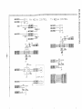
7. PRINTING
OF THE REPORT
AND LISTS
7-1. Activity repod
1. Press ~-EN~
4 times.
IACTIVITY
REPORT?
I
2. Press FE-T
L_J
ACTIVITY
REPORT
3. Activity report is issued.
Sample of activity report
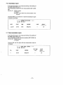
* * * ACTIVITY REPORT * * *
Jun. 26’9312:00
TRNS. TOTAL PAGE 000003
RECV: TOTAL PAGE 000002
No.
TRNS.
DATE
1
2
START TIME
Jun. 26
Jun. 26
No.
9:00
10:00
REGV.
DATE
1
2
Jun. 26
Jun. 26
7-2. One-touch
3. Press ~~
AAA
BBB
2
1
START TIME
PARTNER
9:30
10:30
ccc
ODD
1’02
0’38
PAGE
PAGE
1
1
RESULT
ERROR CODE
OK
OK
RESULT
ERROR CODE
OK
OK
dial list
1. Press ml
2. Press ~
1’23
0’45
PARTNER
5 times.
.
dial list is issued.
Sample of one-touch
dial list
o
*
●
ONETOUCI+
QIAL
LjsT
Jun. 26’9312:00
No.
1
2
3
MODE?
O.T
DIAL
SET
?
.
I
4. One-touch
SET
PARTY’S NAME
AAA
BBB
ccc
NUMBER
000222333
444555666
777888999
–34–
● ●
*
O.T
DIAL
LIST
I
7-3. Speed
b
dial list
1. Press ~ENUj
2. Press ~
5 times.
SET
MODE
?
O.T
DIAL
SET
.
?
3. Press m]
ISPEED
DIAL
SET
?I
4. Press ICOPYI .
I
S.D
DIAL
LIST
I
5. Speed dial list is issued.
Sample of speed-dial
list
➤-
Jun. 26’931200
No.
1
2
3
PARTY’S NAME
AAA
BBB
ccc
——...
‘L7-4. Feature
switch
1. Press -15
NUMBER
000222333
444555666
777888999
—
.—.
-.
—.—
“-”
list
times.
ISET
MODE
?
DIAL
SET
I
2. Press ~
10.
3. Press -j
T
FEATURE
SW. SET
FEATURE
SW.
4. Press ml.
5. Feature switch list is issued.
Sample of feature switch list
* * *
FEATURE SW. LIST
* * *
Jun. 26’9312:00
L.
L
?
\
4 times.
SWITCH NAME
PAUSE TIME
REPEAT CALL(TIMER)
REPEAT CALL(REDIAL)
NUMBER OF RINGS
REMOTE RECEIVE
FAX/PHONE CHANGE
HOLD BUTTON MELODY
VOICE RESPONSE
KEY SOUND
HEADER PRINT
PRINT DENSITY
CLOSED NETWORK (RX.)
INITIAL (RESOLUTION)
INITIAL (CONTRAST)
REPORT (TX.)
REPORT (TIMER TX.)
HALFTONE QUALITY
EDGE ENHANCEMENT
LANGUAGE
TAS CHECK TIME
ZOOM COPY
AUTO TX.
PAPER SAVE RATE
FAX/TEL PARALLEL CONN.
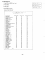
SW No.
SET CODE
01
05
06
07
06
09
10
16
17
20
23
26
27
28
31
32
36
37
48
49
50
54
55
57
03
03
02
02
00
03
02
INITIAL SET
03
03
02
02
00
03
02
01
01
01
00
00
03
03
00
01
01
01
01
01
:
03
03
00
01
;
01
00
01
01
00
00
:
00
01
01
00
00
—
—35—
LIST
?
7-5. RAM CODE LIST
1. Press ~
and -1
(over 1 sec.)
INITIAL
SET
?
L
2. Press -1.
RAM
3. Press WY]
RAM
Sample of RAM CODE LIST
—
*
4
FUNKT
*
* RftM CODE LI’3TE
(=!..
.
,93
SCHQI-TER
10N
+ ‘+ *
SS33
PWSENDWER
HOERER RLRRM
WRHLWDH. ZEITUERSETZT
01
E12
05
WRHLWDH, SOFORT
06
STE1-1-UNEi
EiF21J4J3~TEl_LLlNG
D3
!21
03
01
a3
a~
03
02
FERNST9RT
08
m
00
FRX/TEL
09
03
MELOD I E
m
m
03
fiz
UOICE
16
01
Ell
17
20
El
El
01
23
26
27
2%
00
00
03
UMSCHRLTER
RESPONSE
TRSTRTURTON
KOPFZEILE
PfiFIERRUSldRHL
GESCHLOSSENE 5ENUTZERGRLIFPE
INITIRLISIEREN
KONTRf2ST GRUNDST.
SENDEBERICHT
SENDE.8ERICHT ZEITUERSETZT
HfILBTON-MUSTER
KONTURENSCHAERFE
SPRRCHE
RNT-PRUEFZEIT
ZOOM KOPIE
RUTO.ST9RT
D1
01
m
OR
00
m
49
m
01
130
00
00
m
@1
!21
00
00
w
no
m
uO
GESCHW. !2NZEIGE
62
MONITOR
!20
@l
37
48
SPRR!3RUCI<-RFITE
COPI. Plows
sT9NDLEITUNG
WFiHLT./BSTZT
IWIRTEN RUF RNTWORT
03
80
01
01
m
E10
n3
a3
31
22
36
50
54
55
60
61
63
00
00
64
03
Q6
03
01
06
@l
CED FREQU.
TCF PRUEF.
INTERU.
FSK PRUEFEN
FEHLER-RRTE
67
68
69
70
71
m
00
01
00
m
E10
01
m
FOLGEFEHLER
FOLGEFEHLER
72
a3
03
73
06
E16
TRREGER ?l_lS PRUEFEN
74
m
06
UET RRTE
75
03
03
KENNUNG SENDEN
DCS SENDEN
76
ml
77
78
79
00
01
m
00
00
02
iB
E14
01
00
66
EPIFF.RFITE
(NRML)
(FEIN)
DCS-TR INTERURLL
RTC-Q INTERURLL
FSK INTERURLL
SENDEPEGEL
DTMF-PEGEL
K9BEL ECJ_IRLIZER
81
82
83
84
m
00
02
10
04
01
GESCHL. GRUPPE
P9PER PRECUT
88
93
08
00
ROm
SET
.
4. RAM CODE list is issued.
T.30
CODE
UERS1ON
9W9.
1-
—36-
00
CODE
LIST
?
7-6. Transmission reporl
..
It can be set to issue or non-issue
according
to the setting
of
the RAM CODE SW No. 31.
The initial factory
00).
SW. No. 31 :00
:01
:02
preset is the non-issue position (SET CODE:
(Non issue)
(Issue)
(Issue only when the communication
occurs.)
Once the SW No. 31 is set to 01 or 02, the transmission
is issued accordingly.
D4E
x**
-l~l~~T
Jm26
’93 1231
STPRT
error
report
YXX
PPRllWR
TIW
PE
RES1-T
ERROR
Jm
26
CWIERA
0’45
1230
1
CODE
K
7-7. Timer transmission reporl
It can be set to issue or non-issue according to the setting of
the RAM CODE SW No. 32.
The initial factory-preset is the issue position (SET CODE 01).
SW. No. 32 :00 (Non issue)
:01 (Issue)
Once the SW. No. 32 is set to 00, timer transmission
not issued.
*x*Tl~_~x
Jm26
lb
STPRT
report is
xx
’931231
PN?lWR
SET TIME
Pm
1230
RE9.LT
kRROR
1
123)
mA
1
—37—
0(
COOE
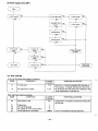
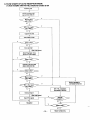
8. FLOW CHART OF AUTO RECEPTION MODE
(1) Auto reception with FAX-TEL switchover function is ON
Y
N
Y
N
r
I
Capture the line
I
t
CNG detect mode
I
1
Voice prompt 1
=5
(See note below)
Send Ring Back Tone
twice and CNG detect
Y
I
EXT.-TEL handeetis
connectedto the line
-
i
(See note below)
Y
A
N
Y
N
—38—
I
Returnto Stand-by
Note @ The following messages are released to the line as Voice prompt.
- Voice prompt 1: Please wait for a moment
- Voice prompt 2: No one is here now, however if you wish to send a fax, please transmit at the tone.
@ Voice prompt is deleted by feature SW. No. 16.
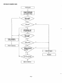
(2) Auto recepth
t
,
I
with FAX-TEL switchover function is OFF
Count incoming ring
signal (RAM SW 07)
I
1
I
N
Built in handset is
connected to the line
Y
I
1
!I
N
I
[
L
Capture the line
I
EXT.-TEL handset is
connected to the line
Y
Send FAX signal
N
)
I
Reception
,
I
[
Return to Stand-by
—39—
1
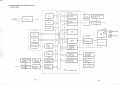
(3) Answer reception mode
Y
N
N
Y
Y
\
N
t
Return to stand-by
N
Y
Detect continuous
-
N
-
1
Reception
u
t
1
I
1
Return tostand-by
—40—
I
L
‘r
T’
L
L-
I
1
I
1
I
I
1
I
1
1
I
I
1
!
I
1
I
I
1
I
1
1
I
I
I
I
I
I
I
I
1
I
I
I
I
1
I
I
1
I
I
~-
---
-------
__[___-,--
-----
---
—
---
r-----l------m
-----___
-1 1
—
---
---------
t
--—- ________ ___ ,_-
L____
I
,-----
----
--
1
A
--
______
1
_ -1
--
____
I
____
I
z
u
I
Ozx
____
:
____
JJo [11
o
z
u)
1+
z H
c1m
ZUJ-I
0+11
-.111]].
OIJZ
lJIJy
.U
11+
<0
Ill IJ
I
1
1
1
I
I
I
I
t
1
I
I
I
1
1
1
I
I
1
1
1
1
1
I
I
I
I
1
I
I
1
1
I
1
I
I
I
I
I
1
1
1
J
D
______
___----I-----
----
----
-1’
_________
i
-z
——
‘N
“,,,,
CO-’
.
3WVd<
c+
,,
-
1
.
w
.::: . .
-13-”-(7WC
,.
ii
A
7’
‘k-l-l’
*.
,,
.,
,.
.,
,,
5
g
,
A
r
.,-.)
{as-c
,
0:
,-
..>
.
[
.
111111
F==2111
L
?
am!mra
“,.
r
‘m’
.0.
IX!*
s.,,
*..,
r
s,,
,!-0.0”/
.,.0/
0.3.0.
.,.”/
,..
%;
..
J.
I ,,.
I
.....
.3,,
1
,
1
H
——
1
“‘—
,
I--zE-l
,
s
((-1+7)-19s9?~E3L
——.
.!,
! .
“’%
.
UI..QEE2
4.!..
.
T31
I
.s.+
w
.,..
v
.,,-
..!.
W4J
A
,,.
,
!
... .=...,.,
.3-
r
,
e
.——
,J
-1
Ml (Main) P.W.B. (3/8)
r.
II
!
Zz
>>
++
$
m
g
y
L
Ill
t]
I
0
[
I
u
-49—
m
I
*
Ml (Main) P.W.B. (4/8)
I
;=-(
No
0;
:
0
Oil.
u
y
.
I
0
I
1
u
—50-
J--l
m
-
.
II
>00
I
<
4
(
(
u
‘“cc
0.
1
C37
2.?OP
❑ 3e
(4-76)
lTxOUT
❑ 40
-a1C14
>
c 35
0.1.
K
6eK
CA1
R39
1
R41
15K
●
~
R45
10K
A
il-
C42
0331J
15K
LA6462
C40
60000
*
n
C39
O.iu
-12”
‘@’
:
‘:F:;
;~
&
R42
2.7K
n43
1.%
v
+.
R
,,Tx
[7-l
B)-
F15.9
1
=5
essl
++
15K
0
I
1C17
4093
(BJ NCU
lCIS
1
s
C101
JP4
0.1”
I
LA646.2
LAS462
&
100K
*–p.J-o-t2v
(7-
16)
_wNz
NCU
C49
O.iu
[POWER]
+24V
+la/—
-12V
+Sv
L
—
—
0
+5”
ICNSI-*3
_l%t%’-’@+””
Av
A
-+/+7
%
‘~(c’cOM.
4 “*l~lu ‘MONOuT
NCU
NC
TRN
_
1
1
Ml (Main) P.W.B. (6/8)
m
I_!
z
—-
Elm
—A
>.*
krr
u:
y:
0
I
I
u
—52—
m
I
4
d
Ml (Main) P.W.B. (7/8)
(Ll
u
r-:
Ht-
a
*
I
>
+><
MiHil
0
I
u
I
—53—
m
[
.
!
B
7
1
I
I
6
5
4
1
1
I
2
I
3
I
-g
~
IC2
uPD65622
L2-7C)
A3
AZ
/.1
AO
CK 3M
‘PH
T
1
,,..-
TPH
TPH
[1
K
TPHC
[c N4-7
1
TPE 1
TPE2
TPE3
TPE4
(6-3C)
STS1
+5”
.00
ICN4-3
HGNO
H(3ND
ICN4lCN4-i
‘v-
●~
N
12-20)
TPH
ST02
STB4
(3-em
6-3c
I
NROM
Ale
NSTB
PRTC
!3-78)
(3-7A)
a
OM 1
OM2
~~&{
(2-7C1
+,,,
OTCK
01
lNT1
(2-2BI
~
u
i7A6
56K
uA6
56K
#INTO
“cc
F196
RXM
rc N5-3
EN3-’3
,
(SENSORI
75-
l/CUT
1
1C9
NCU
IPCF
1
E
‘4c’3TB0N
6
➤ PA5
m
~A4
77.
●PA3
PC7
Pce
PCS
PC4
PC3
PC.2
NCU
PAZ
PA1
P&o
PC1
Pco
NC
NC
/?7
(
I
[
1
A
.-
31
~R1OFF
lC1.?
NCU
[c N3–.25
I
10
i
e
7
I
4
1
5
I
6
1
,
I
3
-,
ail
F
n:
L
c
I
02
n:
D
CN2
CN
‘N
:N2
CM
.N
-N
D
-4
-
:7
-
~
~+’”
1
/7’7
+5V
C201
0.1”
L:o
F---7
o
1
I
[
2
D201
N
G::
BuZZER
1,
Ic N21-14
CN21-15
ICN21-17
/+
II
4
6
5
8
1
19
1*1#
I
REDIAL
PAUSE
SPEED
DIAL
I
SPEAKER
I Ui
In,
1
I
SET
J
1
I
II
IN,
START
1
+~
1,
Y
ANSWER
MOOE
CONTRAST
-1
1
n
11
13
L___;
(01)
(05)
ICN?I-16
;::
Inr
COP
y.
+Bz
t
HOLD
I
MENU
I
1
1
(02)
(03)
(04)
(06)
(07)
(08)
9
—;:;
1,
;
L---
n
10203
-,DWAOiO
74 HC138
“v=
Nc
Ic N21-2&
s
7
[
a
I
I
6
5
4
I
1
I
3
1
I
2
g
~
x’%‘ ‘\-._v,n
0301
2SC3330
---4
L.
0P
vA301
VR61B
---.E!5
*:wn
RL A
i%=%’%
F
~TxL1w
5(’
I
+“
*C314
IZLE
AP033i2
PQ1a-24v
~----,
\
PS2509R307
c309,1
0,
It
;#T~~50v
27K/
zD3JOl
‘“
zy302
QzAJay
1 ‘–
GzA1ey
-----4
,
1
EN3.?-7
ITFI 2J
~N%!-S
INC
‘LINE
‘=3”2
‘
R317
I
-“”
150K
R3ie
RLC
C2
M2
1~
~U
.5VC
R306
100K/iw
rcN3.?-e
~
a~‘.;;;;O
Pc301
L--------
2
16
C31B
AFB07F1000D1
6B0
r-l
~
~
W@’”
IETEI
1CN31-
41
n315
ICN3.2-2
,7]
$3;;
I
—
ICN31-
4+
’2”
‘“”e
UWA-301!3
IL2
!
C330
NC
/
RLG
~N32-3
ICN31-B
H?
R322
!5. SK
NC
4
I
i’
:’
-----——
‘L
.
‘“”
J= —
‘
1
C3.23
HZ44
lIJ/50v
a.
,5956P
I
+12V
0301
ICN31-5
I
i+i2V
J
ERA15
+.24VC
+12VC
pL---L
p~
R
L
EAB
ICN31-131+5V
D
[CN31-181-12V
6
J
I
+5VC
ERA
~-lzv
==75”’
0305
I
15
[0
= !?%2%
2%7,5.
3
[CN31
N
N
-1410GND
1
dP302
[c N31-151AGND
~
1
@
DGND
1?
/77
lCN31--
1
(
1
7
I
6
I
6
,
5
4
I
I
3
2
1
1
~-.------
1
~QW-SrL ,
JRd 13
1
1
C40.2
gE73:/250v
lK
IHSK21
,
❑ 40
I
!
560
I
M.J41-6
CN41-6
1.
PI
::;,.
0.
R41
=-6
0GZB7
T
ZD409
~]
.-
I
INC
1
R416
9.i
K
~~~~
1
,
~d~
Ocso
J
0.027
I
~
:-
: .~5:s
56
‘“~’”
1/.2N
C401
1000II
CERAMIC
O
*
~
,~
SB;g:~O
40e
sB0015
,~’-+
-03.
R412
C413
056u
ZD401
: ;
_
0
220.
~ C4i6T
-03A
00
0.
l_____
VCc
VL
g
0. OIBU/!50V
C41B
c417
lK
10
0.0.22.
50v
:
C432
1/::
~
3300 D-
To1
FIO1
TOO
!?02
~
NC
~
AC BIAS
~
C431
3300.
T
24-
!
❑4iJ3Ak
NC
22
r0260
BT1
MFIN
15000
,1
~~
BPO
c1
~
~
clip:.
r-+~
is
7
TPO
RP1 1
18
s
TP1l
RPI,
‘7
?
I
,
ZD404
J
“W
.F14.29
“ .20K
405
C405
‘,:”:0=
3 ‘K
n
100”/6
9
3V
TP12
y&2
F!435
~
-.l~
C421
R432
0.02.2LI/50v
;N43-3
W41-1
I+5vC
r’
1!=
S6T0260
&141-3
4J41-4
dJ41
-5
7,5K
*5VL
C420
o.0i8u/50v
‘“*+
IL
IFTEL2
0
100”/6
~‘
1
I
I
x4
~~~
&b.
W
I
4=s
I
4W4A01
C411
C426
1
1
~4.7u/25v
*
IL
180.22”
W::
;L *
Ic N4
1-3
c425
fEL
1
EL2
[c N41-4
I
ICN4 1-2
I
-
3.
~
FC2
GNO
FC1
VCC
IN
VDi
SW402
1
L406
P
I
lcN43-4
iMONOUT
1C403
MC34f19
O,iu
c42e
1
---J
;
X4
RI-26.2X2
200
ZD40?i
~
- - c430T
t
A.
“v
m4.22
7,SK
HANDSET
1
e~O
‘
i
1
”/50v
1./29.
RA07
=.04
__--:
,
SPE4KER
❑ 414
1C402
TA31065FA
l/2w
R40~
1
----~402
❑ 411
ZD408
%6
VA”
lK
0
7K
F!413
2.20
f4Ls73x4
L--.i.-
I /DHS
Ri421K7
ZD402
fi’”
;N43-7
5
~Bx2’50
{Hwi,l~~~~
30 It%zore
4.
IYE!
0
I R
N“
m
lBLACK
1’z
1
0ss-
f&/~OV
c4i4
ST401
+
i
MI C +
MICL:
1.emH
0.056.
.IP41
i/ew
la4a3
1/2w
PI
INC
.4,,
1/2w
C412
t
TEL1
TEl_2
c,,,
1
L413
CN41-8
CN4 1--
~w~
“~d
%-
,
,,1000
-
SPEAKER
6
7
I
e
k N51 -4
PA
RX
~7
EN51-5
l/sPs.7
~
1
SIZE
Nc
d
PAPER
MECHA
CONTROL
SENSOR
TX
[cN61
r
MECHA
1
I
2
I
=.
I
4
1
5
I
s
I
CONTROL
-14
+s”
~---l
I
I /92
“-tS2
020
S3
%
NC
+24”
zD601
+5V
TX
MVR
Mvi3
~
T
~g
4+’
,
Vv
::
~
+.?4 v
R.
Z0501
+5”
MVR
Mv
OZB16C
MOTOR
ICN52-3
-4
‘c”’
cN61-221/TMl
1
1
~:c,:
DODD
lCSO
i
LB i205
!7’7
L601
CN61–1BI+24V
/+7
CN61–191+5V
R503
f:-C-0+24V
-----------------
!
1
I
I
1
v
OUTA
3
IDCMG
CM
/OuTA
g
D
1C502
TA842aK
I
A7
~
Ic N53-1
I
1
1
1
OC
HO1OR
CIS
1
!
4
,
+9;
; CUTER
UNIT
~
CN61-9
CN6 i-e
CN61-7
CN6 1-6
CN61-5
~
~
~
~
—
~
CN
-4
—
I
ICN51 -3
l/CUT
fi/cuTG
L501
A
CN51-12!+24V
CN51-111+5V
/’?7
ICN53-4
‘---------------’
t
1
I
I
CN61-2
~r
VD
VI-ED
CN63-10
MOTOR
lCN6e-3
ICN62-4
{
z
UJ
M7 (Power Supply) P.W.B.
,>>>
!
1111
m*mru
...-4
1111
.4
r.,.
p$
u
-(.+-!
t.r.
d+-
u
-
L
n
I
1
)
(3) PWB Wiring Diagram
M7 (Power Supply) P.W.B.
—60—
,,
,,,:
,,
,1
,,,
,..,
,,.,
,’
...
,,
I
,..
I
I
I
I
.
ii
(4) Abbreviated
signal explanation
SIGNAL NAME
FUNCTION
DO-D7
LCD data bus
E
LCD data enable
RS
LCD register selector
BZON
BZ
/STOP
COLO-2
/ROWO-3
LPERR
LPANS
/DHS
Buzzer signal
Buzzer power supply
Stop switch
Key scan column
Key scan row
Error LED
Answer mode LED
Internal handset hook up detection
RIMUTE
Ringer signal mute
SPMUTE
Monitor mule
MONOUT
Line
SHORT
HZ44
/ HS
PCE1
EARTH
Circuit short signal
Daial tone/Busy tone detection
External TEL hook up detection
Ringing signal detection
Circuit earth signal
Dial pulse signal
Connect modem to line signal
Reception signal
Transmission signal
Monitor signal
TPH. power supply
] CONNECTION
I
NOTES
CN2-CN21
(CN22-LCD)
CN2-CN21
(c::2;~:)
f;;;;~;y)
8~L
RXLINE
TXLINE
MONITOR
HV
monitor
/CUT
TPH. serial data
TPH. serial clock
TPH. strobe signal
TPH. thermistor output
TPH. thermistor GND
Cutter motor forward
Cutter motor reverse
Cutter wait position
IPAP
ISPSZ
/JAM
Recording paper stock detection
Recording paper size detection
Recording paper jam detection
/RMlo–3
(RMOO-3)
VLED
Reception motor pulse signal
(Reception motor drive signal)
LED drive voltage for CIS
GLED
LED GND for CIS
CLK
Clock for CIS drive
SI
Scan signal for CIS drive
VIDEO
Video image signal
/s1
/s2
Document stock detection
Document read position detection
Document size detection
Transmission motor pulse signal
(Transmission motor drive signal)
Thermal head power ON signal
Thermal head power GND
Speaker drive signal +
Speaker drive signal -
DATA
CLOCK
/sTB1-2
THM
THMG
CUTF
CUTR
1s3
/TMlo-3
[yoy-3)
HGND
SP+
sP-
ON Low
CN2-CN21
CN2–CN21
CN2-CN21
CN2-CN21
CN2-CN21
CN2-CN21
CN3-CN31
(CN32-CN41)
CN3-CN31
(CN32-CN41)
CN3-CN31
(CN32-CN41)
CN3-CN31
(CN32-CN41)
CN3-CN31
CN3-CN31
CN3-CN31
CN3-CN31
CN3-CN31
CN3-CN31
CN3-CN31
CN3-CN31
CN3-CN31
CN3-CN31
CN4-TPH
(CN7-CN71)
CN4–TPH
CN4–TPH
CN4-TPH
CN4-TPH
CN4-TPH
CN5-CN51
CN5-CN51
CN5-CN51
(cN53-cu-rrER)
CN5-CN51
CN5-CN51
CN5-CN51
~C54~:;~
SENSOR)
(CN52-RX MOTOR)
CN6-CN61
g:i3;::)
(CN6;-CIS)
CN6-CN61
(CN63-CIS)
CN6-CN61
(CN63-CIS)
CN6-CN61
(CN63–CIS)
CN6-CN61
CN6-CN61
CN6-CN61
CN6-CN61
(CN62-TX MOTOR)
CN7-CN71
CN7-CN71
CN43-SPEAKER
CN43-SPEAKER
—63—
Key ON: Low
Key ON: Low
Key ON: Low
LED ON: LOW
LED ON LOW
HOOK UP LOW
Mute High
Mute High
Analog signal
ON High
Detect: High
HOOK UP: LOW
Detect: AC signal
ON: High
ON: High
ON High
Analog signal
Analog signal
Analog signal
ON: LOW
ON Low
ON High
ON Low
ON Low
ON Low
ON Low
Analog signal
ON: LOW
ON: LOW
ON: LOW
ON High
Analog signal
Analog signal
0
,. ..,,,
,,,
,,’
’,.
,’, ,, ’,.
,.’
.
,’.
.“
..
.,
...
”
SPECIFICATIONS
(1) IC configuration
UPD65622
I
UPD 65622
r--
1
I
PPPPPPPPVGNSSSSP
AA AA AA AA
01234567DDTBBBBT
DNSTTTT
R
—
PCIRT
A
PORT
E3
PORT
C
PA7-PA0
B1234C
64
STBI
TPEI
TPE2
TPE3
TPE4
PB7
PB6
P95
PB4
PB3
63
62
61
60
INTO
PE32
PB 1
PBO
PC7
PC6
PC5
GNO
PC4
Pc 3
PC2
Pc i
Pco
NROM
AI.9
ROM2
ROM 1
NRAM
A16
!5k3
DI
INT1
TPHC
Pc7-Peel
=:
55
CLKD
GND
TPHI
CKIM
54
!i3
.
CONT
5TFIOEE
STB4—5TE31
!32
5L
CK3M
TESN
TCLK
1=
50
4’3
4f3
~Fl
F
CNTO
N.C
NUCS
NCS
AO
Al
A2
RAM3
I
59
DTCK
UP D65622
PB7-PBO
~AU7-ADO
47
4S
-45
44
43
41
41
E
RAM3-RAM1
r==l
$FiCIMCS
}
CONT
RAM
AMCS
‘pE4-TpEo
ROM2–ROM1
1.-u3E4
2
5
STBINT
TPH;
J
#tIIII1II1I1111
II811
III
1Ill
1I:11
t
1111111111111111111111111111111111111111
VAAAAAAACVPI
Pin Assignment: ~ , , , “,
* 6 4 3 1 10s
I II
444444441333>1
7 b 6 # >3
I 0S
DlVVUT7TTtlVA
AAAAAAAVAAAAAA
AllDSAF.C~CUUO
I)
KAI)SPSSSSCCUO
g;~
Vcm
.,
\
;AO-–
I)I)I)lD1)OIISLLL
LLLLLL1)I.8911
1134L61S0
1114
111
II
111111
o
2 1 O*11
lIIISXXXXXXX
66?K11X
01134
o
#b
RuRIS
bSlll13Z1Q
1!
DqA
99011:
IIU
T
L
1-
Ill
Illllllllloooo
4 J 2 1 0S0?
6 643
AACVCAAAAAAAA
:~;;;::
.T N-.
-q
33332221111211
0S,7
66
6 6 4 1 1
81
,s
1.
1-
TEST Mode
f
/noMcs ~
Address Data !WS
- \ Rack-up
h4R acc;ralor
MR
Vss
KA8
mArP
;;
*9
s
~ACIW
~E
!,
*%%t=&
lms
CXXN
VDO
CXO07
{ALARM
Itfn
:,
1
04T1
ml-s
M~!or
TC35168BF
TOPVIEW
1/0
Control
I
Vss
Moo
Mol
MOI
MOX
MIo a
MI*
~,,
~
U19
Voo
Iwn
1)474
Im’i
INN
~JL
m
ma:
mt
mslw
cut
xl
Vss
X1
IMAGE
PROCESSOR
2% :fl,o-/
-lo&
Vf.,.
-m&
*,”,
J9L
:g,”
9SAVn
S!18111)
I 23
4b
T
o
PITTT
r000ti4,
fii:VCPFWKCKCVEC
670
PP
rPr
?llllllll[
rr
YYV
Pr
):,:
LIPLll)CVt~~!RT~~
:Vti$$$i~V
* Itr(nllllllllillllllll
1?11312’4
11
I1111111
V1>s
YlBTRStl
TIJBU11RSII11
01
1 34*s7an
SSLlt
PSKll
,4
,
-
:Pu
T1‘:
~
‘,
.
=+
‘HER::,”+,,
‘“”EMA;~5!j
-E
“v
Ah
BRA:
AA:
VVICVEVVCVA
-
‘7
,:
“&V’nm
:Cruscx
-.. ..— 1= ~
I
Q)
:
SC
Ult
AM
MN
DNL
T111D4KTti
012346*1
All
AA
Tot
1>>231333>
@ *012116
—64–
I! N3fi
18(1
AYCXXCTTD
TCfl
UUD8
d78D
2444
011
lCCCUI)S
VL143?TS
44444446$6
1466199082
Syatam Block Diagram
-E@
I
“c’”:tint
=
Conwol
EyePattern
MonitorCircuit
T
d
TuRBO
]
II I
I
m
EEcl
II pa
II
CPU
X’tal
125MHZ
-1
. .. 0
.
El ““” 00
.
TLcs-90 CPU
n
RTc
Xtd
32kHz
lm*ge
Processor
I.-J
cCD
Cls
n
~u r
20.?36MHz
XWI
Module
$hzding
Meme.y
4.=s2
I
-Q&l
RAM
P
—L
IEJ
7W14
TOP VIEW
I
TOP VIEW
TC4584
f
Vcc
IN B
lY
IN A
3A
Vcc
GND
OUT Y
2Y
TOP VIEW
TC4053BP/ll
F
TC4053
u
4-I’..
OY
lZ
z-
Cou
02
INN
%
,ss
2
15
~-cOM
3
14
X-COM
4
u
lx
~
23
ox
~
11
A
v
10
B
e
90
Coukmsl
A
B
~
I
ml
UON
UON
-
—65—
SYSTEM DI AGRAN (74HC138)
74HC138
A
1
la
s
2
16
c
3
~2A
4
&B
6
al
8
w
7
QNO
8
II
14
13
12
11
10
9
(TOP VIEW)
LC3564
BLOCK 01 AGRAM(LC3564)
a,
t, ~
d,
&.
8.,
a,
1,
8,
C-s,
f
40&ld*r
mo
I
.
I
C.l”ml
I“pl
I
6,
I
M*
I
C.”1,.l
I
\
nA
A.
:
.
w<
Vss
I
I
TiJA#,
+
Wn.e, Mel,..
ls~m
3
1
C.1.nm 0?,04,,
,1
II
I
1
I
x
1{0
-
;
\
T(XJ VIEW
27CO!0
AS
\~
27CO1O
1024x 1024
X-oecodw
A9
MemoryMatfta
A12
10
A16
A
Uooo
\
I
Input
Y. Gatmq
mu
*7T~
Y.Oecoda
control
II
~
—66—
II
:H,gh,hr,,holdl””,,,,r
.,,
TA75558
LA6462
RC082BM
Retn~;k:
Vcc line
of
are shorted
pin
mdNo.9
fb.1
i nternal
I
y.
M51957
M51957
n
I
~7vcc
2
#
n
w
NC 3
@g34
----
-
~ljNc
NC}O
INPUT
-——
G
r-
1fWUT
6 ~~T
5 DELAY CAPACITOR
TOP VIEW
DELAY CAPACIT(M
MC341 19
r
MC341 19
CD
FC2
FCI
Vin
1
8
V02
.— ---
----
6 Vcc
Y
-----
1
D
2
7
Gnd
3
6
Vcc
4
5
Vol
{Top View)
L ----- --— Gnd -- —-t=
a
TC35123
‘Do
Wuu
TXOUT
Vssl
MUTE
DPDMCK
DPDMDT
PD
J-a
“1”’
RXINA
2
15
3
14
V!W2
4
13
AGC5
5
12
AGC4
6
11
A6C3
7
10
APDMDT
8
9
APOMCK
H
TOP VIEW
--F: ‘
TXOUT
MUTE
—67—
#
DA
X
DPDMDT
}
) DPDMCK
I
BLOCK OIAGRAM
(MC34012)
APPLICATI(XY CIRUJIT
——— ———_
r
O,ode8r!dge
L
IAC1
I
___
—ti &___
~US
‘Ri---
ifi,
.
--1
i;–––
I
I
I
,
7.0 v
AC2
,,
SCR
Trmwment
I
Threshold
~
/
I
I
Comparator
Clamp
I
.
I
+
I
J
Tone
Osctllalor
:
-
Frequenr,v
I
onflder
‘ RC
!
+’+
;
-
I
E141.
MC3401 4
:“’’’’”
F retIttencv
L ____________
Owwler
..! G-’_
‘“~
––
__;
TA8428K
v..
--@
GNO
--@
—
I
J
I
I
I
I
))41
S-8051ANR
-------- . . . . . . . . . . .,------ . . . . . . . . . . -------,
#
BLOCK DIAGRAM (S-8051ANR)
,.. ..- ----- . . . . . . . . . . . . . . . . . . . . . . . . . . . ----- . . . . . . . . . . -. .
,
,,t
I
I
,
,I
1. OUT
,
2. VDD
,
,
I
*
,
,,
,
1
2
,
. . . . . . . . . ------------
m
,,,
,
3. V33
OUT
VREF
3
. . . . . . . . . . . ----------
-.
,
,
1
‘--”----”-----”--”------------”&-------------------~
VDD
—68—
V33
(2) Parts specification for power supply
(3) Figure of main parts for power supply
Q701, 702
Ref. No.
I
Kinds
I
.~ames
------1.
D704
-- ... .. .R!!!Y
Transistor
Q701
Power MOS FET
Q704
Q702
Power MOS FET
2SK1 545
:
ID
:
2SC3330T
Vceo
Ic
2SJI 75
VDSS
2SC4048
Vceo
Ic
: 50V
: 0.2A
: 60V
: IOA
: 50V
:O.l A
ID
Q703
800V
3A
VDSS
D701
Rectifier Stack
D2SBA60
Vrm
10
: 600V
: 1.5A
D702
High speed
ERB44-08
Vrm
10
: 800V
: 1A
D704
Low
ESAC92M-02
Vrm
10
: 200V
: 10A
Vrm
10
: 200V
: 0.5A
10SS
I ERA91 -02
D703, 705,
’06, 707
_–l-—--——-–.–
T Zener diode
ZD701 , 702
GZA30X
Vz
Pc
ZD703
DZB27C
ZD704
GZA5.6X
ZD705
GZA5. 1x
ZD706
GZA4.7X
Vz
Pc
Vz
Pc
Vz
Pc
Vz
Pc
: 30V
: 0.5W
: 27V
: lW
: 5.6V
: 0.5W
:5.1 V
: 0.5W
: 4.7V
: 0.5W
Ii!
aaaa
IC703
1
Input
Common
[
1------
output
IC702
Ic
IC701
Ic
FA5310P
IC702
MC34166T
Vout
lout
: 5V
: 3A
IC703
Down chopper
regulator control IC
Voltage regulator
TA78L012AP
Vout
lout
: 12V
: 150mA
“C704
Voltage regulator
TA79L012P
Vout
lout
: -12V
: 150mA
L
I Photo Coupler
r
L.n.e
Q703, 704
Cathode
IC704
Diode
P701
node
-
t)
PC120
Isolation Voltage
: 4kv
P701
—69—
output
Input
Common
12. TIME CHARTS OF EACH COMMUNICATION
(1) HIGH SPEED MODE
(A)
MODE
MANUAL TRANSMISSION
STARTSW
t
‘aLmlNCUJ
T DISP
(B)
MANUAL
——--- CASE
.—— ~ —MODEOIANGE
_
RECEPTKN
START SW
CML-RELAY{NCIJJ
,,,$P
~
~1
SENO SIGNAL
CEO
w“
:f&E~VE
~~
I
I
I
CFR
‘0S
USWDCS VR=hl!OM=L
TR
W-RELAY
(NCU)
R DISP
~
.Cso
W!J
TEL RESERWTION
n
VICEO
(OTHERS 2) [ CALL UP AFTER
1
VmEo
mm
SIGNAL
n
PR1-oPM-O
n
ml-o
n
PIP/PIN
PHONEIAMP
(OPERATOR
W-L)
OPERAmRCALL
HOOKOPF
wcu)
R-SIOE
UPFROMR-SIDE
T-SIDE
n!
MCFI
CFR
was
NcU)
(E)W
OCN
d
,~
SENDSIGNAL
CML-Y
RTC E@
—~
(D) CALLUP FROM T-SIDE
RECEIVE
MCF
+.,-;
SENo
SIGNAL
RECEIVE
-L
CML-REIAY
I
mNG TCNE RING lUNE DETECT
txWPREcE’vE
(2)
CFR
———
AUTO RECEPTION
(C)
I
mwm
HOOKDFF
—70–
SENDING)
I ul
RTC EOP
DCN
13. SIGNAL
(I)
FLOW CHART
HIGH
SPEED MODE
A) MANUAL
B) MANUAL
T/R
T/AUTO
R
C) MULT 1 PAGE
T/R
E) PHONE RESERVATION
(CALL
UP FROM T-SIDE)
R
T
:,?uME~J
HOOK OFF
T
rl--%+
I
MPs
~
p
RTL
I
m-a
I
MI-Q
WmAm cut.
~p/plN
7R41NING
Kmaom
1
VIDEO
@
D) CHANGE MODE
L
I
@@
sPunllmuK
I
Ii
ir ,
F) PHONE RESERVATION
V13’EO I
(CALL UP FROM
d\
#
vI DEO
A
~
VIDEO
R
T
4
*
R-SIDE)
M
HOOK OFF
(MESSAGE)
m
OFmAma
CAu.
‘“”
‘ -c’mti~l-h=,
.
—71 –
m
P-l
I
SFUMTAU
I
14. EXPLODED
I
VIEW
I
2
1
3
I
4
I
5
@
d
b
FIGUREP
—72—
I
I
2
3
I
I
4
I
5
L
\~
\
w
“- -n
d
12
I
‘@3
‘@3
—
,-0
@
13
a’
21
m
Bll‘
0’
s??
&-----&d
—
‘e?!$
FIGUREB
—73—
“V---6-A
—
f
E12
.
—74–
15. PARTS LIST
PRODUCT SAFETY NOTICE
Eachprecautioninthismanualshouldbefollowedduringsewicing.Componen@identified
withthelECsymbol Aintheparts listandtheschematic
diagramdesignatecomponentsin which safetycan be of special significance.When replacinga componentidentifiedwith A, use only the
replacementpartsdesignated,or partswith the sameratingsof resistance,wattageor voltagethat are designatedin the partalist in this manual.
Leakage-current or resistance measurements must be made to determine that exposed parts are acceptably insulated from the supply circuit before
returning the product to the customer.
Ref.No.
I
I
PART No.
DESCRIPTION
INDIVIDUAL
INDIVIDUAL CARTON CASE
STYRO-FOAM CUSHION, RIGHT
STYRO-FOAM CUSHION, LEFT
HANDLE
PAD, HANDLE
POLYETHYLENE BAG, 570X550
,UNIT
POLYETHYLENE BAG, 265X41 O
,HAND SET
BAG,POLYETHY-FOAM 31OX340
,CASE 3
IABEL, RECYCLE CORRUGATE
IABEL, GREEN POINT
WIRE HARNESS, CURL 280MM
WIRE HARNESS, 3000MM,LINE
OR
CORD, LINE 3000 MM,LINE
}
INSTRUCTION MANUAL,GERMAN
POLYETHYLENE BAG, 285X41 O
,INSTRUCTION MANUAL
ROLL PAPER, A4 15M
LABEL, ONE TOUCH
INDICATION LABEL,REC PPR1
INDICATION IABEL.REC PPR3
INDICATION LABEL;ORGI.JAM
LEAFLET
INDICATION IABEL,REAR CVR
6326681800
6326645581
6326645598
6323011608
6326069240
6326374115
6326374160
6326734445
:12
6326356685
6326627174
6326573204
6326448939
6326617663
6326734315
6326374160
6326517633
6326645635
6326734322
6326734339
6326734346
6326462607
6326734452
6326734469
6326719480
6326730119
6326770496
Ref.No.
at)
—
1
1
1
1
1
Al 3
PART
DESCRIPTION
No.
KNOB, TEL
SCR S-TPG BIN 3X6,
CABINET-MECHANISM
SCR S-TPG BIN 3X8,
CABINET-BOTTOM LID
GUIDE, PAPER
BACK LID
SCR S-TPG BIN 3X4,
BACK LID
COVER,CABINET
SHEET, B
PANEL
SIGN WINDOW
PIATE SPRING
SCR S-TPG BIN 3X6
KNOB, TENKEY
KNOB, MODE,SHORTENING KEY
KNOB, FUNCTION
KNOB, ONE TOUCH
KNOB, COPY
SHEET, FPC
SHEET, FPC ) ‘R
SCR S-TPG BIN 2X6
SCR S-TPG BIN 2X6
BRACKET, PANEL
COVER, PANEL
SCR S-TPG BIN 3X8
SCR S-TPG BIN 2.6X5,
PANEL BRACKET-M2 PCB
SCR S-TPG BIN 3X6,
PANEL COVER
6326538463
4110012106
4110256609
Al 4
Al ~
6326735268
6326643921
4110272203
Al 6
Al 7
Al 8
Al 9
A20
6326741603
6326711965
6326691878
6326691885
6326396544
4110256104
6326735275
6326642436
6326735329
6326642450
6326539415
6326693179
6326642375
4110254209
4110254209
6326642405
6326769577
4110256500
4110271503
1
1
1
2
1
1
1
1
1
1
1
1
1
1
1
1
1
1
1
1
2
AM
A22
A23
A24
A27
A28
A28
A29
A30
4110256203
MECHANISM
CABINET
!1
,4
,5
BOTTOM LID ASSY
RATING LABEL
BRACKET, EARTH
SCR S-TPG BIN 3X6,
BRACKET-BOTTOM LID
SCR BIN 4X5, EARTH
SCR PAN+SW 4X6,
POWER-AC CORD-EARTH
WASHER OUT TW 4,
AC CORD-EARTH
WASHER OUT TW 3
SCR S-TPG BIN 3X4
SCR S-TPG BIN 3X6,
POWER PCB
SCR S-TPG BIN 3X6,M1 PCB
SCR S-TPG BIN 3X6,M3 PCB
SCR S-TPG BIN 3X4,M4 PCB
SCR S-TPG BIN 3X6,
MECHANISM 2
SCR S-TPG BIN 3X6,
MECHANISM 1
COVER, ROLL PAPER
GUIDE, R
GUIDE, L
GEAR, GUIDE
SCR S-TPG PAN+W 2X5,GEAR
SCR S-TPG BIN 3X4,
ROLL PAPER COVER
KNOB
CABINET
BRACKET. SPEAKER
SCR S-TPG BIN 3X6
6326805862
6326681824
6326643891
4110256104
4111256707
4110461003
4110060501
4110080402
4110272203
4110256104
4110256104
4110256104
4110272203
4110256500
4110256500
6
7
8
9
77
11
12
6326735299
6326735305
6326735244
8326366886
4111242809
4110272302
6326735312
6326735251
6322769229
4110256104
NOTES
—
1
1
1
1
1
2
B1
B2
6326643938
6326643945
B3
4110272203
6326643976
4110285609
&
M
1
2
1
2
2
1
1
2
2
1
1
1
1
1
2
1
1
2
E
B7
B8
BI 1
BI 2
B13
BI 4
B15
B16
B17
B18
B19
B20
B21
B22
B23
B24
B25
B26
6326644003
6326361146
6326361153
4111011207
6326361160
6326361177
4110256104
6326361207
6326644034
6326644041
6326644058
A 6322502802
6326361245
6326361252
6326361269
6326361276
6326361263
6326252635
6326644065
4110271305
6326362662
6326362679
6326709818
6326486573
6326449400
4111520907
1. Part orders must contain Model Number, Part Number and Description.
2. Ordering quantity of screws and resistors must be multiple of 10 PCS.
—75—
O’ly
1
3
3
1
1
2
1
2
1
1
1
1
1
1
1
2
3
1
1
‘1 o
2
1
;
1
2
1
CHASSIS,
T RIGHT
1
CHASSIS ASSY, T LEFT
SCR S-TPG BIN 3X4, MOTOR
GUIDE, PAPER 1
SCR S-TPG PAN 2.6X4,
GUIDE-CHASSIS
BRACKET, SENSOR
BRACKET, SHAFT, 1
SHAFT, ADF
RING E 5,ADF SHAFT
BRACKET, SHAFT
ROLLER, ADF
SCR S-TPG BIN 3X6
KNOB
BRACKET, SHAFT
PLATEN, SENSOR
PLATE SPRING, CIS
WIRE BAND,
GEAR, 1
GEAR, 2
GEAR, 3
GEAR, 4
GEAR, 5
GEAR, 1
GUIDE, PAPER 2
SCR S-TPG BIN 2.6X4,
CHASSIS-GUIDE PAPER 2
BRACKET, BRAKE, 1
BRAKE, ADF
PIATE SPRING, ADF
BRACKET, BRAKE, 2
COIL SPRING
SCR S-TPG BIN 2X4
1
2
1
4
1
1
1
~.,.1
1
1
2
1
2
:
1
1
1
1
1
1
.1
1
2
1
1
1
1
2
2
.
Ref.No,
027
026
B29
B30
PART No.
6325811624
6326709399
6326711941
4110272203
B32
633
B34
B36
636
B37
IB39
B40
641
642
B43
B44
645
B46
B47
B46
B49
WI
B51
352
B53
654
B65
S56
657
S56
B69
SHAFT ,MECHANISM l-PANEL
INSULATOR,FFC
SHEET, BRAKE 2
SCR S-TPG BIN 3X4,
MECHANISM 2 PCB-EARTH
SHEET, BRAKE 1
6326445174
I
631
DESCRIPTION
MECHANISM
6326644096
4110272203
6326644119
6326682081
4110271305
CHASSIS ASS’Y, RIGHT
SCR S-TPG BIN 3X4, MOTOR
CHASSIS, REC LEFT
BRACKET, PAPER 2
SCR S-TPG BIN 2.6X4,
BRACKET-CHASSIS
PL4TEN, HEAD
BRACKET, SHAFT
GEAR, 1
GEAR, 1
GEAR, 2
BRACKET, HEAD HOLDER
SHAFT. OPEN
LEVER; OPEN R
LEVER, OPEN L
TORSION SPRING, LEVER
SCR PAN+FLG 2.6X4
BRACKET, HEAD R
BRACKET, HEAD L
SCR PAN+FLG 3X4
SPACER,THERMAL HEAD
GUIDE, PAPER
INSUIATOR
SCR S-TPG BIN 2.6X4
PIATE SPRING, HEAD 2
SCR S-TPG BIN 3X4
TORSION SPRING, R
TORSION SPRING, L
SHAFT
GUIDE, PAPER R
GUIDE, PAPER L
SHEET, PAPER,
t3RACKET pApER I
PAPER CUTTER ASS’Y
GUIDE, cuTTER I
WASHER Y 3X8X0.5
GUIDE, CUTTER 2
SCR S-TPG BIN 2.6X4,
GUIDE-CUTTER
WIRE FIXTURE
GUIDE, CUTTER 3
SCR S-TPG BIN 2.6X4,
GUIDE-CLHTER
SCR S-TPG BIN 2.6X4.
PAPER CUTTER-CHASSIS
SPACER
SPACER
SCR S-TPG PAN 3X14,M5 PCB
FIXTURE,JAM SENSOR
SHEET, A
WIRE BAND,
SCR S-TPG BIN 3X4
SHEET, C
6326644133
6326644034
6326252635
6326361245
6326361252
6326644140
6326644157
8326711972
6326644184
6326644171
4110474506
6326644166
6326644195
4110476609
6326711903
6326644201
6326696549
4110271305
6326363506
4110272203
6326644218
6326644225
8325811624
6326460580
6326460597
6326644232
6326730508
6326644256
4110904104
6326644263
4110271305
6322500855
6326644270
4110271305
4110271305
660
B61
B73
6323061625
6323066585
4110287601
6322616592
6326711958
A 6322502802
4110272203
6326762763
L
B76
B64
B65
B79
6326748176
6326666054
6326752203
6326668061
B67
6326666108
B66
669
B70
6326766958
6326758472
8326660933
6322543409
6326868115
B71
2
CHASSIS ELC.
THERMAL HEAD
WIRE HARNESS, I05MM ,CN4
PULSE MOTOR
WIRE HARNESS, 65 MM,
CN5-CN51
JUMPER LEAD, 15P 140MM,
CN5-CN51
SENSOR ASS’Y, IMAGE
WIRE HARNESS, 10P 180MM
PULSE MOTOR
LUG ,CIS-CHASSIS
JUMPER LEAD, 23P I15MM,
CN6-CN61
Ref.No.
Q~
2
1
1
1
A31
A32
& 6326766972
6326668092
A33
6326668047
1
—
1
2
1
1
4
1
2
1
1
1
1
1
1
1
1
2
1
1
2
2
1
2
2
3
3
1
1
2
1
1
2
1
1
1
1
1
2
1
2
1
2
2
2
2
1
2
2
1
—
—
1
1
1
1
1
1
1
1
2
1
PART No.
A34
A35
A42
DESCRIPTION
AC CORD ASSY, 21OOMM
JUMPER LEAD, 28P 255 MM,
CN2-CN21
WIRE HARNESS, 160MM,
CN7-CN71
HOUSING, 6P ,CN32-CN41
TERMINAL ,CN32-CN41
CORE ,CN32-CN41
LIQUID CRYSTAL DISPLAY
SPEAKER, 160HM
SOCKET, 2P 90MM
TERMINAL, EARTH
6323012324
6322876408
6325827483
6326675502
6322496729
6326666098
6326370629
1
1
1
2
16
1
1
1
1
2
PC BOARD 1
A36
Icl
IC6
IC2
(IC3)
IC3
IC4,5
6326736500
4093081108
4092810400
4101678304
6326366530
4101748007
4091370608
PWBOARD
ASSY,M 1MAIN
ICTC35168BF
ICTC35123F
ICUPD65622GF-043-3B9
SOCKET,
IC32P
ICTMS27CO1OA-15JL/9801A
ICLC3564PML-12OR
IC4,5
IC6
Icl 1
Icl 7
Icl 7
IC9
IC9
Icl 3
Icl 3
Icl 4
Icl 4
IC15
Icl 5
IC16
IC16
IC7
IC21
CN2
CN3
CN4
CN5
CN6
CN7
Swl ,2
L1,2,3
XTALI
XTAL2
XTAL3
BAT
BAT
Q1
Q2
Q3
Q5,6,7
D1,2,3
4091464703
4092977301
4091558105
4090512900
4091554206
4090746909
4091761901
4090394704
4092416200
4090185302
4090494602
4090185302
4090494602
4090185302
4090494602
4090749603
4093076706
6326661468
6326661512
6322539969
6326666036
6326661475
6326422571
6326368268
6325889528
6326370766
6322507579
6326480533
6326366547
6326741269
40504413501
4050161900
4050476402
4050162402
4070041000
4070694909
4031542904
4040497707
4040497707
4031646204
4032044407
4031848006
4031571904
4031554204
4031397306
4031459905
4031572604
4031572604
4031572901
4031572901
4031572901
4031129303
4031130507
4031130507
4031576602
4031133605
IC LC3564PML- 15
Ic TC7W14F
Ic TC7SU04F
Ic TC4053BF
Ic BU4053BF ) ‘R
IC TC4584BF
OR
IC BU4584BF
IC NJM082BM
OR
IC RC082BM
1
IC IA6462M
IC TA75556F
‘R
IC LA6462M
IC TA75558F ) ‘R
IC IA6462M
IC TA75558F
‘R
Ic M51957BFP
IC S-6051 ANR-NB
CONNECTOR, 30P
SOCKET, 20P
PLUG, 15P
CONNECTOR, 15P
CONNECTOR, 23P
PLUG, 16P
SLIDE SWITCH
CORE
CERAMIC OSC., 12,5 MHZ
CRYSTAL OSC., 32.766KHZ
CRYSTAL OSC., 20.736 MHZ
LITHIUM CELL
LITHIUM CELL
‘R
TR 2SA151O
TR 2SC3395-TA
TR 2SD1623-T
TR 2SC3398
DIODE DCCO1O
DIODE DSBO1O
10U M 10V
OS-SOLID
ELECT
IOUM
16V
10UM
16V
ELECT
10U M 25V
ELECT
10U M 50V
ELECT
47U M 6,3V
ELECT
10P D 50V
CERAMIC
15P J 50V
CERAMIC
18P J 50V
CERAMIC
22P J 50V
CERAMIC
30P J 50V
CERAMIC
30P J 50V
CERAMIC
47P J 50V
CERAMIC
47P
J 50V
CERAMIC
47P J 50V
CERAMIC
100P J 50V
CERAMIC
220P J 50V
CERAMIC
220P J 50V
CERAMIC
470P K 50V
CERAMIC
CERAMIC
1000P K 50V
&l
C7,8
C47,62
C3,4
cl
C5
C25
C70
Cl 6
Cl 7,69
C13,14
C104
C73-76
C77-81
C64-93
C44,55
C37,46
C51
C16
cl 2
—
NOTES
Q’ry
1. Part orders must contain Model Number, Part Number and Description.
2. Ordering quantity of screws and resistors must be multiple of 10 PCS.
—76—
1
1
)
1
1
1
1
1
1
1
1
2
2
1
11
1
1
1
1
1
1
1
1
1
1
1
1
1
1
1
1
1
1
1
2
3
1
1
1
1
i
1
1
1
3
3
1
1
2
2
2
1
1
1
1
1
2
2
1
4
5
10
2
2
1
1
1
/
—
—
—
I
Ref.No.
I
PART No.
4031134109
4031577302
4031551807
4031942603
4032620502
4032247006
4031640204
4031640204
4031640204
4031640204
4031640204
4031640204
4031640204
4031640204
4031640204
4031640204
4031840204
4031640204
4032220306
4031925905
4031925905
4031925905
4031925905
4031925905
4031658708
4011057909
4011057909
4011057909
4011057909
4011057909
4011057909
4011057909
R56,90
4010375004
C103
4011055606
JP17
4011051907
R22
4011052706
R25
4011054007
R51
4011050504
R2,4
4011050504
R17,21
4011050504
R34,52
4011050504
R94
4011051501
R43
4011052805
R1,3
4011052805
R15,96
4011052805
R103
4011052805
R92
4011053307
R42
4011058001
R68
4011054601
R18
4011051600
R24
4011056605
~44
‘6
4011057404
. . ,19,204011050603
4011050603
R23,29
4011050603
i R30,31
R40
4011050603
4011051600
R39,41
4011051600
R55
4011058203
R45
4011138400
R46
4011052904
R35,93
4011052904
R67,69
4011058104
R7,8,9
4011058104
R11,12
4011058104
RI 3,28
4011058104
R32,33
4011058104
R82,83
4011056104
R89,97
4011058104
R104
4011056104
R105
4011055400
R60
4011057503
R5,54
4011050702
R50,58
4011050702
R95
4011051709
R62
4011054304
R14
4011054809
R6
4012121708
R36,38
I
CERAMIC
CERAMIC
CERAMIC
CERAMIC
CERAMIC
CERAMIC
CERAMIC
CERAMIC
CERAMIC
CERAMIC
CERAMIC
CERAMIC
CERAMIC
CERAMIC
CERAMIC
CERAMIC
CERAMIC
CERAMIC
CERAMIC
CERAMIC
CERAMIC
CERAMIC
CERAMIC
CERAMIC
CERAMIC
MT-GLAZE
MT-GLAZE
MT-G14ZE
MT-GLAZE
MT-GLAZE
MT-GIAZE
MT-GLAZE
MT- GIAZE
MT-GIAZE
MT-GIAZE
MT-GLAZE
MT-GIAZE
MT-GLAZE
MT-GLAZE
MT-GLAZE
MT-GLAZE
MT-GLAZE
MT-GLAZE
MT-GIAZE
MT-GIAZE
MT-GLAZE
MT-GIAZE
MT-GLAZE
MT-GLAZE
MT-GIAZE
MT-GIAZE
MT-GIAZE
MT-GLAZE
MT-GLAZE
MT-GIAZE
MT-GLAZE
MT-GIAZE
MT-GIAZE
MT-GLAZE
MT-GLAZE
MT-GLAZE
MT-GLAZE
MT-GLAZE
MT-GIAZE
MT-GIAZE
MT-GLAZE
MT-GLAZE
MT-GLAZE
MT-GLAZE
MT-GLAZE
MT-GLAZE
MT-GLAZE
MT-GLAZE
MT-GLAZE
MT-GIAZE
MT-GLAZE
MT-GLAZE
MT-GLAZE
C36
C40
C23
C58
C41
C2
C6,9
C15,19
C21 ,22
C24,28
C32,33
C39,42
C43,45
C49,50
C52,57
C59,83
C29-31
C38
Clo
C35,48
C26,27
c101
’102
)9
11
JP3,4
JP7,8
JP9,1O
JP15
f JP20
NOTES:
DESCRIPTION
Ny
—
2200PK
50V
6800PK
50V
0.01 U K 25V
0.015U K 25V
0.033U K 16V
0.047U Z 50V
0.1 U Z 25V
O.l U Z 25V
0.1 U Z 25V
O.l U Z 25V
0.1 U Z 25V
O.l U Z 25V
O.l U Z 25V
O.l U Z 25V
0.1 U Z 25V
0.1 U Z 25V
0,1 U Z 25V
0.1 U Z 25V
0.22U K 16V
0.1 U K 25V
0.1 U K 25V
0.1 U K 25V
0.1 U K 25V
0.1 U K 25V
lUZ
16V
0.000 2A 1/16W
0.000 2A 1/16W
0.0002A 1/16W
0.000 2A 1/16W
0.000 2A 1/16W
0.0002A 1/ 16W
0.000 2A 1/16W
0.0002A 1/ 10W
56 JA1/16W
160 JA 1/16W
220 JA 1/16W
330 JA 1I16W
lKJA1/16w
lKJA1/16w
lKJA1/16w
lKJA1/16w
1,5K JA 1/16W
2.2K JA 1/16W
2.2K JA 1116W
2.2K JA 1/16W
2.2K JA 1/16W
2.7K JA 1/16W
5.6K JA 1/16W
3.9K JA 1/16W
15K JA 1116W
6.8K JA 1t16W
6.2K JA 1116W
10K JA 1/16W
10K JA 1/16W
10K JA 1/16W
I OK JA 1/16W
15K JA 1/16W
15K JA 1/16W
68K JA 1/16W
75K JA 1/16W
22K JA 1/16W
22K JA 1116W
56K JA 1/16W
56K JA 1/16W
56K JA 1/16W
56KJA l/16W
56KJA l/16W
56K JA 1116W
56K JA 1/16W
58K JA 1/16W
47K JA 1116W
82K JA 1116W
lOOK JA 1/16W
lOOK JA 1/16W
150K JA 1/16W
330K JA 1/16W
390K JA 1/16W
24K FA 1/16W
1
1
1
1
1
1
2
2
2
2
2
2
2
2
2
2
3
1
1
2
2
1
1
1
1
2
2
2
1
1
2
2
1
1
1
1
1
2
2
2
1
1
2
2
1
1
1
1
1
1
1
1
2
2
2
1
2
1
1
1
2
2
3
2
2
2
2
2
1
1
1
2
2
1
1
1
1
2
—
Ref.No,
PART No.
DESCRIPTION
4012121807
4012037009
4012173606
4012175404
4011853600
6328857751
6326657476
6326386538
6326657751
6326657476
6326386538
6326020821
6326564745
6326315835
4030093100
4030890705
R37
R48
R28
R27
R91
RAI -4
RAl -4
RAl -4
RA6,7
RA6,7
RA6,7
RA5
RA5
L4
Cllo
Clll
MT-GLAZE
75 KFA1116W
MT-GLAZE
604 FA1/16W
MT-GIAZE
27 KFA1/16W
MT-GUUE
47 KFA1/16W
MT-GIAZE
2.2KJA I12W
RESISTOR BLOCK, 56KX4
RESISTOR BLOCK, 56KX4
OR
RESISTOR BLOCK, 56KX4 }
RESISTOR BLOCK, 56KX4
RESISTOR BLOCK,56KX4
OR
RESISTOR BLOCK, 56KX4 1
RESISTOR BLOCK, 22KX4
OR
RESISTOR BLOCK, 22KX4 )
CORE, 60 OHM
IOOPJ 50V
CERAMIC
CERAMIC
1000PK
50V
1
PC BOARD 2
A37
6326789483
IC201
IC201
BUZZER
CN21
CN22
D201
D202
D203
LED201
LED202
JP201
-206
R204
R201
R203
R202
C201
C202
4091751308
4091751605
4200011408
6326661451
6328430255
4071395904
4071395904
4070852909
4071597100
4071597209
4010354106
MT-GLAZE
180 JA 1/8W
MT-GIJZE
180 JA 1f8W
MT-GIAZE
330 JA 1/8W
MT-GIAZE
4.7K JA 1/8W
CERAMIC
O.lu z 50V
CERAMIC
O,lu z 50V
TERMINAL EARTH,
M2-CHASSlS(90MM /50MM)
1
IC302
IC303
IC303
IC304
Q301
CN31
CN32
CN33
IA301
-304
IA301
-304
ZD301
ZD302
D301
-306
:303
2306
:305
2309
2310
:311
1
1
1
1
1
1
1
1
1
1
6
1
,1
1
1
1
1
2
—
8326736517
6325198453
6326833087
6326736937
6326737903
6322573116
8322573116
6325529950
6326737996
4071629601
4090198005
4092576504
4101782407
4090494701
4090185203
4101045007
4050179501
6326661536
6322540033
6326690734
4070459607
PW BOARD ASSY, M 3 NCU
TRANSFORMER, MODULATION
TRANSFORMER
REIAY ,CML
OR
RELAY ,CML
REIAY ,DP
REIAY ,SRL
REIAY ,LOOP
REIAY ,EARTH
PHOTO COUPLE PS2565-1 -V
IC LB1234
IC LBI 234ST
‘R
Ic AFB87F1OOOD1
IC TA75558P
OR
IC LA6462D
IcAFM94F440C15
TR 2SC3330-S
PLUG, 20P
PLUG, 6P
WIRE HARNESS, 7P 100MM
VARISTOR VR-61 SS )
1
1
1
1
1
1
1
1
1
1
1
1
1
1
1
1
1
1
1
1
4
4070459409
VARISTOR VR-61 B
4
4070497807
4070497607
4070059203
ZENER DIODEGZA18;
ZENER DIODE GZAI 8Y
DIODE ERA15-04
4031619200
4031673509
4031619101
4031733005
4031497006
4031497006
MT-POLYEST 0,22U K 250V
MT-POLYEST 0,56U K 250V
MT-POLYEST 0.047U K 250V
MT-POLYEST 0.33U K 250V
MT-POLYEST 0.022U K 250V
MT-POLYEST 0.022U K 250V
1. Part orders must contain Model Number, Part Number and Description.
2.Ordering quantity of screws and resistors must be multiple of 10 PCS.
—77—
1
—
1
PC BOARD 3
A38
r301
T302
RLA
RLA
RLB
RLD
RLG
RLE
PC301
IC301
IC301
1
1
1
1
4
4
4
2
2
2
1
1
1
1
1
—
—
PW BOARD ASSY, M 2
OPERATION PANEL
IC SN74HC138NS
OR
ICTC74HC136AF )
PZ BZR PKM22EPP-2WI
CONNECTOR, 30P
CONNECTOR, 16P
DIODE FC903
DIODE FC903
DIODE DWAOIO
LED SML-O1OVT ,RED
LED SML-O1OMT ,GREEN
MT-GLAZE 0.000 2A 1/8W
4010359202
4010359202
4010364701
4010388303
4030702705
4030702705
6326370629
)?
—
1
1
)
)
}
‘R
1
1
6
1
1
1
1
1
1
—
—
Ref.No.
PART No.
DESCRIPTION
My
Ref.No.
PART No.
DESCRIPTION
O’t)
—
C314
C320
C315
C316
C313
C318
C317
C319
C321
C322
C324
C308
C326
C329
C328
C323
R303
R304
R301
R307
R306
R315
R316
R317
R321
R312
R322
4030820405
4030093100
4030020502
4030020502
4030606201
4030023602
4030013009
4030013009
4030013009
4030013009
4030013009
4031886006
4031391908
4030446609
4031096407
4031096308
4010946006
4010666607
4010946709
4010993307
4010935703
4010275205
4010273003
4010252305
4010247400
4010247400
4010272800
6326370629
POLYESTER 0.047U K 50V
100P J 50V
CERAMIC
CERAMIC
1000P K 25V
CERAMIC
1000P K 25V
POLYESTER 3300P K 50V
CERAMIC
0.1 U K 25V
CERAMIC
O.l UM 16V
CERAMIC
O.l UM 16V
CERAMIC
O.l UM 16V
CERAMIC
O.l UM 16V
CERAMIC
O.l UM 16V
NP-ELECT
220U M 16V
ELECT
10U M 25V
ELECT
10U M 25V
ELECT
10U M 50V
ELECT
lUM
50V
OXIDE-MT
82 JB 2W
OXIDE-MT
220 JB 2W
OXIDE-MT
560 JB lW
OXIDE-MT
27K JB lW
CARBON
100KJB
lW
CARBON
680 JA 1/6W
CARBON
56K JA 1/6W
CARBON
150K JA 1/6W
CARBON
10K JA 1/6W
CARBON
10K JA 1/6W
CARBON
5.6K JA 1/6W
TERMINAL, EARTH,
M3-CHASSIS(150MM)
{
PC BOARD 4
A39
6326736524
IC401
IC402
IC403
D401
D404
ZD406
ZD41 O
D402
D403
ZD409
ZD401
ZD402
ZD404
ZD405
ST401
ARR401
ARR401
ARR402
ARR402
Z404
HS
SW401
SW402
Bz
MJ42
MJ41
CN42
CN43
CN41
L413
L414
L401
L404
L406
L407
L409
-412
0SC401
0SC401
C402
C403
C411
C408
C405
4082796902
4092947007
4092032602
4070096109
4070096109
4070096109
4070096109
4070040807
4070773109
4070773109
4070513507
4070513507
4071561808
4071561808
4070109403
6326601501
6328808234
6326172292
6328543900
6328357699
6326519950
6326386275
6326386275
4200010906
6322515949
6322515983
6322539976
6328890758
6322540033
6328375204
6326375204
6325499291
6325499291
6325499291
6325499291
6325499291
PW BOARD ASSY, M 4
TELEPHONE
IC SAA1094-2
IC TA31065FA
Ic MC34119M
DIODE RLS-73
DIODE RLS-73
DIODE RLS-73
DIODE RLS-73
DIODE DCBOIO
DIODE SS001 5-03A
DIODE SBOO15-03A
ZENER DIODE GZB7,5B
ZENER DIODE GZB7.5B
ZENER DIODE RLZ6.2B
ZENER DIODE RLZ6.2B
DIODE S1WBA60
DISCHARGE TUBE
DISCHARGE TUBE 1 ‘R
DISCHARGE TUBE
OR
DISCHARGE TUBE 1
DISCHARGE TUBE
PUSH SWITCH, HOOK
SLIDE SWITCH
SLIDE SWITCH
PIEZO BUZZER PKM33EP-I 001
SOCKET, 4P
SOCKET, 6P
PLUG, 2P
PLUG, 7P
PLUG, 8P
COIL
COIL
CHOKE COIL, 60UH
CHOKE COIL, 60UH
CHOKE COIL, 60UH
CHOKE COIL, 60UH
CHOKE COIL, 60UH
6328356364
6328386480
4031733005
4030877805
4031392202
4031295800
4031346100
CERAMIC OSC., 455 KHZ
CERAMIC OSC., 455 KHZ ~ ‘R
MT-POLYEST 0.33U K 250V
MT-COMPO
0.47U J 50V
ELECT
4.7U M 25V
ELECT
22U M 35V
ELECT
100U M 6.3V
L
NOTES
1
1
1
1
1
1
1
1
1
1
1
1
1
1
1
1
1
1
1
1
1
1
1
1
1
1
1
1
—
—
1
1
1
1
1
1
1
1
1
1
1
1
1
1
1
1
1
1
1
1
1
1
1
1
1
1
1
1
1
1
1
1
1
1
1
1
4
1
1
1
1
1
1
1
—
C407
C404
C408
C41 o
C401
C428
C419
C415
C418
C420
C422
C417
C421
C414
C412
C413
C416
C425
C426
C427
C429
R407
R411
R419
R401
JP411
C423
R412
R423
R431
R436
R436
JP41O
JP412
JP413
JP415
JP416
JP419
JP420
R408
R404
R416
R413
R415
R414
R408
R433
R439
R443
R430
R421
R405
R422
R432
R416
R428
R434
R417
R440
R435
R424
R426
R429
R444
R442
R445
R427
JP
4031346100
4032086308
4031212609
4031080000
4030757101
4030095807
4030695601
4030709803
4030713503
4030713503
4030713503
4030662007
4030682007
4030725902
4031303802
4031303802
4031925905
4031925905
4032220306
4031858708
4031858708
4011131906
4011819408
4011511807
4011837501
4010354106
4010375004
4010375004
4010375004
4010375004
4010375004
401037 5fx14
401037 5CQ4
4010375004
4010375004
4010375004
4010375004
4010375004
4010375004
4011050009
4010375202
4010380008
4010380802
4010389805
4010390304
4010375400
4010375400
4010375400
4010375400
4010385102
4010386408
4010387700
4010389704
4010389704
4010391004
4010376803
4010376603
4010376803
4010376803
4010378005
4010379309
4010385300
4010360206
4010386505
4010387304
4010378104
4010379408
6326781937
ELECT
100U M 6.3V
ELECT
220U M 16V
ELECT
220U M 16V
ELECT
0.22U M 50V
CERAMIC
1000P K 500V
CERAMIC
100P J 50V
CERAMIC
0.01 U K 50V
CERAMIC
0.01 5U K 50V
CERAMIC
0,016U K 50V
CERAMIC
0.018U K 50V
CERAMIC
0.018U K 50V
CERAMIC
0.022U K 25V
CERAMIC
0.022U K 25V
CERAMIC
0.027U K 50V
CERAMIC
0.056U K 25V
CERAMIC
0.056U K 25V
CERAMIC
O.l U K 25V
CERAMIC
O.l U K 25V
CERAMIC
0.22U K 16V
CERAMIC
lUZ
16V
CERAMIC
lUZ
16V
MT-GLAZE
15JA l/2w
MT-GLAZE
56 JA 112W
MT-GLAZE
150 JA 1/2W
MT-GLAZE
560 JA 1/2W
MT-GIAZE
0.0002A 1/8W
MT-GIAZE
0.0002A 1/lOW
MT-GLAZE 0.000 2A 1/lOW
MT-GLAZE 0.000 2A ?/lOW
MT-GLAZE 0.000 ZA 1/lOW
MT-GLAZE 0.000 2A 1/lOW
MT-GLAZE 0.000 2A 1/lOW
MT-GIAZE
0.0002A 1/lOW
MT-GIAZE
0.0002A 1/lOW
MT-GIAZE
0.0002A 1/lOW
MT-GLAZE 0.000 2A 1/ 10W
MT-GIAZE
0.000 ZA 1/lOW
MT-GLAZE 0.000 ZA 1/lOW
MT-GLAZE 0.000 ZA 1/lOW
MT-GLAZE
lKJA l/2W
MT-GLAZE
100 JA 1/lOW
MT-GLAZE
200 JA l/10W
MT-GIAZE
220 JA l/10W
MT-GLAZE
750 JA 1/lOW
MT-G L3AZE 620 JA 1/1 OW
lKJA l/10W
MT-GWWE
MT-GLAZE
lKJA1/10W
MT-GLAZE
lKJA1/10W
MT-GLAZE
lKJA1/10W
MT-GLAZE
3.9K JA 1/lOW
MT-GLAZE
4.7K JA 1/lOW
MT-GLAZE
5.6K JA 1/lOW
MT-GLAZE
7.5K JA 1I1OW
MT-GIAZE
7.5K JA 1/lOW
MT-GIAZE
9.1 K JA 1/lOW
MT-GLAZE
12K JA 1/lOW
MT-GLAZE
12K JA 1/1 OW
MT-GLAZE
12K JA 1f 10W
MT-GIAZE
12K JA 1I1OW
MT-GLAZE
15K JA 1I1OW
MT-GIAZE
16K JA 1I1OW
MT-GLAZE
39K JA 1I1OW
MT-GLAZE
20K JA 1/1 OW
MT-GLAZE
47K JA 1/lOW
MT-GLAZE
51 K JA 1/lOW
MT-GLAZE
150K JA 1/lOW
MT-GLAZE
180K JA 1/lOW
JUMPER LEAD, 114MM
1
1
1
1
1
1
1
1
1
1
1
1
1
1
1
1
1
1
1
1
1
1
1
1
1
1
1
1
1
1
1
1
1
1
1
1
1
1
1
1
1
1
1
1
1
1
1
1
1
1
1
1
1
1
1
1
1
1
1
1
1
1
1
1
1
1
1
1
PC BOARD 5
B74
6326738658
CN54
CN55
CN53
CN52
6326666005
6322540088
6322540088
6322540095
6322540118
1. Part orders must contain Model Number, Part Number and Description.
2. Ordering quantity of screws and resistors must be multiple of 10 PCS.
—78—
PWBOARD
ASSY,M 5
RX.MECHANISM
CONTROL
PUSK!3WITCH
,PAPER
SWITCH
PLUG,3P
PLUG,3P
PLUG,4P,CUTTER
PLUG,6P,MOTOR
1
1
1
1
1
1
d
---
—
Ref.No.
PART No.
DESCRIPTION
Ref.No.
crly
PART No.
DESCRIPTION
)?
—
1
1
CONNECTOR, 15P
IC LB1205-L
IC TA6428K
ZENER DIODE DZB16C
CARBON
470JA l/6W
CARBON
820JA l/6W
ELECT
10UM
16V
ELECT
33UM
35V
TERMINAL, EARTH,
M5-CHASSIS(l 10 MM)
6326661499
4091240804
4092344004
4070471104
4010269600
4010278305
4031391502
4031359007
6326370629
CN51
IC501
IC502
ZD501
R502
R501
C501
C502
I
1
1
1
1
1
1
1
I
—
PC BOARD 6
B75
S2
S1
CN62
CN63
CN61
IC601
ZD601
C601
L
CM2
—
PW BOARD ASSY, M 6
TX. MECHANISM CONTROL
PUSH SWITCH
PUSH SWITCH
PLUG, 6P
PLUG, 10P
CONNECTOR, 23P
IC LB1205-L
ZENER DIODE DZB16C
ELECT
10UM
16V
ELECT
33U M 35V
TERMINAL, EARTH,
M6-CHASSIS(60MM)
163266’3 7580
6326666234
6326666012
6322540118
6322540057
8326661505
4091240604
4070471104
4031391502
4031359007
6326370629
C716
C718
C721
C713
CR702
C727
R701
R702
R703
R705
-708
R709
R717
R71O
R711
R714
R713
R715
R716
R719
R718
R720
R721
R712
CN71
CN73
1
,
1
1
1
1
1
1
1
1
1
1
—
PC BOARD 7
A40
6326734278
T701
L701
L702
L703
F701
6326696051
6326736289
6326509104
6326616608
4230059500
6325630964
(F701)
Z701
Q701
6326212363
4071527008
4051192608
6326207154
4051106209
4050370809
4050179600
4080164607
4071155003
4070080100
4070071403
6326207154
4070502105
4070502105
4070472002
4070505403
4070504703
4070503607
4093067209
4071613404
4071607007
4071613305
6322469365
4240025007
6328437315
4040549703
4040549703
4040268901
4040268901
4040269108
4040269108
4040269108
6325921402
4031837604
4040601401
4032684009
4032053805
4032161508
4032378007
4032376007
Q702
Q703
Q704
D701
D702
D703
D704
L
ZD701
ZD702
ZD703
ZD704
ZD705
JP705
IC701
P701
TH701
TH701
VR701
TF701
C702
C707
C703
C706
C705
C708
C709
C712
C71 o
C711
C714
C720
C715
C717
u
—
PW BOARD ASS’Y, M 7 230V
POWER SUPPLY
INVERTER TRANSFORMER
CHOKE COIL, 0.020H
CHOKE COIL, 0.01 H
CHOKE COIL, 160UH
FUSE
250V 2A
CAUTION LABEL, CAUTION,
HEAT SINK P
HOLDER, FUSE
VARISTOR ENC471 D-05A
TR 2SK1 545
CORE ,Q701 (G,S)
TR 2SJ175
TR 2SC4048
TR 2SC3330-T
DIODE D2SBA60(4004)
DIODE ERB44-08
DIODE ERA91 -02
DIODE ESAC92M-02
CORE ,D704(1 ,3)
ZENER DIODE GZA30X
ZENER DIODE GZA30X
ZENER DIODE DZB27C
ZENER DIODE GZA5.6X
ZENER DIODE GZA5.1 X
ZENER DIODE GZA4.7X
Ic FA531 OP
PHOTO COUPLE PC120FY2
THERMISTOR M6R21OD
OR
THERMISTOR M8R21OC
PRESET RESISTOR, 6.8K
FUSE THRM 250V 2.5A 115C
BRACKET, HOLDER, TF701
MT-POLYEST 0.22U M 250V
MT-POLYEST 0.22U M 250V
CERAMIC
2200P M
CERAMIC
2200P M
CERAMIC
4700P M
CERAMIC
4700P M
CERAMIC
4700P M
CORE ,C705(A),C709(E)
CERAMIC
150P J 2K
ELECT
66U M 400V
ELECT
1U M 350V
ELECT
47U M 35V
ELECT
10OOU M 35V
MT-COMPO
0.1 U J 50V
MT-COMPO
0.1 U J 50V
1
NOTES
1
1
1
1
1
1
1
2
1
1
2
1
1
1
1
1
1
1
2
1
1
1
1
1
1
1
1
1
1
1
1
1
1
1
1
1
1
1
1
2
1
1
1
1
1
1
1
—
4030567108
4030829101
4030817306
4032659809
6325756244
4032439706
4010203901
4010879601
4010879601
4010937707
POLYESTER 10OOPJ 50V
POLYESTER 6800P J 50V
POLYESTER 4700P J 50V
CERAMIC
880P K 2K
coMPoslTE,c&R,l
000P,220HM
ELECT
4.7U M 50V
470K JA 114W
CARBON
270K JA 1/2W
CARBON
270K JA 1/2W
CARBON
OXIDE-MT
15K JB lW
4020637703
4010126006
4010224005
4010123407
4010163708
4010201907
4010183807
4010183807
4010183607
4010125609
4010192908
4010136308
4010263905
6326422571
6322537880
6326642511
6326642504
6325706768
6322875722
6326370629
4110014506
MT-GIAZE
0,1 J- 2W
100KJA l/4W
CARBON
66K JA 114W
CARBON
10JA lf4W
CARBON
CARBON
3.3K JA 114W
4.7K JA 114W
CARBON
CARBON
3.3K JA 114W
3.3K JA 114W
CARBON
3.3K JA 114W
CARBON
lKJA I14W
CARBON
CARBON
39K JA 1/4W
12K JA 114W
CARBON
330 JA 1/6W
CARBON
PLUG, 16P
PLUG, 2P
HEAT SINK, P ,Q701
HEAT SINK, S ,D704,1C702
TERMINAL EARTH ,A
TERMINAL ,A,G
TERMINAL, EARTH ,G
SCR S-TPG PAN 3X8,
D704,Q701
CHOKE COIL
Ic MC34166T
OR
IC MC34167T )
IC TA78L012AP
DIODE ERA91 -02
6326648674
4093066907
4093091600
4090500709
4070060100
1
1
1
1
1
1
1
1
1
4
1
1
1
1
1
1
1
1
1
1
1
1
1
1
1
1
1
1
2
1
2
I
1
1
1
1
3
I
4032137208
4032168301
4032168301
4032378007
4010223008
4091116800
4032251805
1
1
1
1
1
1
1
—
ELECT
10OOU M 6.3V
100U M 25V
ELECT
100U M 25V
ELECT
MT-COMPO
0.1 U J 50V
6.8K JA 114W
CARBON
IcTA79L012P
47U M 25V
ELECT
J
PC BOARD 14
976
6326640296
4071264101
6326666081
—
1
1
1
PW BOARD ASSY,JAM SENSOR
PHOTO COUPLE GP2L22B
SOCKET, 3P 225MM
I
I
I
PC BOARD 15
B80
CN55
(CN55)
6326745670
4071264101
PW BOARD ASSY, REMAIN
PHOTO COUPLE GP2L22B,
PAPER REST SENSOR
HOUSING, 3P
TERMINAL
6323012270
6322876406
1
1
1
1
3
I
$
HAND SET
—
1
A41
El
E2
E3
E4
E5
E6
E7
E7
E6
E9
6326733325
6326538494
6326539460
6326095393
6322934221
6326348734
4110260507
4110262303
6326466834
4070507605
4070538807
6325011004
6325377056
6326392355
6326348741
1. Part orders must contain Model Number, Pari Number and Description.
2. Ordering quantity of screws and resistors must be multiple of 10 PCS.
—79—
HAND SET ASS’Y
CABINET ASSY
BOTTOM LID
COVER
WEIGHT
BRACKET, SPEAKER
SCR S-TPG PAN 2.6X1O
SCR S-TPG PAN 3X1 O
MICROPHONE
ZENER DIODE GZA9.1 X
ZENER DIODE MTZ9.1 B
JACK
JACK ) ‘R
SPEAKER
COVER, MICROPHONE
A
(1)
1
‘R
(1)
(1)
(1)
(2)
(1)
(1)
(1)
(1)
(1)
(1)
(1)
(1)
I
Ref.No.
El O
El 1
El 3
NOTES
I
PART No,
6326346756
6323413244
6326632468
I
DESCRIPTION
CUSHION, RUBBER, SPEAKER
CUSHION
FIXER, MICROPHONE
a’ly
(1)
(2)
(1)
1. Patiorders must con@in Model Number, Pati Number and Description.
2. Ordering quanti~of screws andresistors must bemultipleoflOpcs.
.
—80—
Jul./’9l/l
500 HO Printed in Japan
SANYO Electric Co., Ltd.
OSAKA, JAPAN
J