1
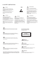
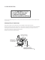
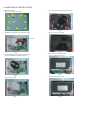
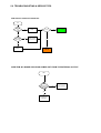
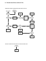
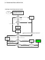
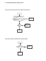
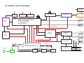
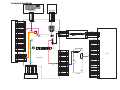
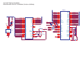
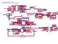
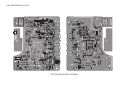
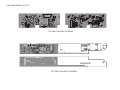
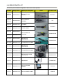
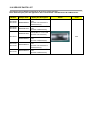
DVD Portable Player
PET706 / PET707
All version
Service Manual
TABLE OF CONTENTS
Chapter
Technical Specification……………………………………… 1
Safety Instructions…………………………………………… 2
Instruction for Use………………………………………………3
Mechanical Instructions……………………………………… 4
Troubleshooting & Service Tips…………………………… 5
Overall Block Diagram………………………………………… 6
Overall Wiring Diagram……………………………………… 7
Electrical Diagram……………………………………………… 8
Component Layout…………………………………………….. 9
Service Parts List………………………………………………. 10
Revision List……………………………………………………. 11
©Copyright 2005 Philips Consumer Electronics B.V. Eindhoven, The Netherlands
OSD
TEST
All
rights
reserved. No part of this publication may by reproduced, stored in a
CONFIGURATION
SETUP
retrieval system or transmitted,
in any form or by any means, electronics,
mechanical, photocopying, or otherwise without the prior permission of Philips
3141 785 31205
Version 1.5
1.0 TECHNICAL SPECIFICATION
General
Dimensions (WxLxH):
Audio CD:
Weight:
Power supply:
18.9 x 14.7 x 3.7 cm
7.5 x 5.75 x 1.5 inches
0.86 kg / 1.89 lb
DC 9V 1.8A
Operating temp. range:
Laser wavelength:
Video system:
0 - 50˚C (32 ~ 122˚F)
650nm
NTSC / PAL / AUTO
Frequency response:
20Hz ~ 20KHz ± 1dB
Signal/noise ratio:
Audio distortion + noise:
85dB
-80(1KHz)
Channel separation:
Dynamic range:
85dB
80dB
Output
Audio out (analog audio):
Output level: 2V ± 10%
Load impedance:
10K
Video out Output level:
1Vp - p ± 20%
Load impedance:
75
Current consumption
DC-IN SUPPLY (9.0V)
Battery Charging Current
1.2A typ.
BATT. SUPPLY (7.2V)
Power Off
0A
Playback with TFT on
<1.2A typ.
Playback without TFT on
<600mA
Battery playtime
>2.5hrs
Headphone out (headphone output load 2x16ohm)
Maximum output power:
Frequency response:
SNR (A-wght):
THD (1kHz):
Left-Right Channel
Separation:
Left-Right Channel
Balance:
Supported disc type
DVD video discs:
Video CD:
>10mW
20Hz - 20kHz
80dB typ.
<1%
32dB typ.
1dB
MP3-CD:
In addition, this unit can play DVD+R & DVD+RW and CD-R &
CD-RW that contains audio titles or MP3 or JPEG files.
You cannot play disc other than the above listed.
(CVD, CD-ROM, CD-Extra, CD-G and CD-I discs cannot be
played on this DVD player)
Software upgrades
For the best performance of your DVD Portable. Check
www.philips.com/support for latest software
upgrades available.
To check the software version of your DVD Portable.
1. Press the SETUP key to enter the setup menu.
2. Press RETURN and then press 1. 2 and 3 on the
remote control.
3. The display will show the software version as the
date of which the software was built on the bottom
of the screen. E.g. 050303
Procedure on how to upgrade the software of the DVD
Portable
1. Download the latest software from the Philips
support site.
2. Unzipped the files and then burn it onto a CD ROM
then playback the CD ROM on the DVD Portable.
Pixel specification
<= 4 (max. 1 bright dots and 3 dark dots)
2.0 SAFTETY INSTRUCTIONS
GB
NL
ESD
WARNING
Alle IC’s en vele andere halfgeleiders zijn
gevoelig voor electrostatische ontladingen
(ESD).
Onzorgvuldig behandelen tijdens reparatie kan
de levensduur drastisch doen verminderen.
Zorg ervoor dat u tijdens reparatie via een
polsband met weerstand verbonden bent met
hetzelfde potentiaal als de massa van het
apparaat.
Houd componenten en hulpmiddelen ook op
ditzelfde potentiaal.
All ICs and many other semi-conductors are
susceptible to electrostatic discharges (ESD).
Careless handling during repair can reduce life
drastically.
When repairing, make sure that you are
connected with the same potential as the mass
of the set via a wrist wrap with resistance.
Keep components and tools also at this
potential.
F
WAARSCHUWING
ATTENTION
I
Tous les IC et beaucoup d’autres
semi-conducteurs sont sensibles aux
décharges statiques (ESD).
Leur longévité pourrait être considérablement
écourtée par le fait qu’aucune précaution n’est
prise à leur manipulation.
Lors de réparations, s’assurer de bien être relié
au même potentiel que la masse de l’appareil et
enfiler le bracelet serti d’une résistance de
sécurité.
Veiller à ce que les composants ainsi que les
outils que l’on utilise soient également à ce
potentiel.
D
AVVERTIMENTO
WARNUNG
Alle ICs und viele andere Halbleiter sind
empfindlich gegenüber elektrostatischen
Entladungen (ESD).
Unsorgfältige Behandlung im Reparaturfall kan
die Lebensdauer drastisch reduzieren.
Veranlassen Sie, dass Sie im Reparaturfall über
ein Pulsarmband mit Widerstand verbunden
sind mit dem gleichen Potential wie die Masse
des Gerätes.
Bauteile und Hilfsmittel auch auf dieses gleiche
Potential halten.
Tutti IC e parecchi semi-conduttori sono
sensibili alle scariche statiche (ESD).
La loro longevità potrebbe essere fortemente
ridatta in caso di non osservazione della più
grande cauzione alla loro manipolazione.
Durante le riparazioni occorre quindi essere
collegato allo stesso potenziale che quello della
massa dell’apparecchio tramite un braccialetto
a resistenza.
Assicurarsi che i componenti e anche gli utensili
con quali si lavora siano anche a questo
potenziale.
GB
Safety regulations require that the set be restored to its original
condition and that parts which are identical with those specified,
be used.
“Pour votre sécurité, ces documents
doivent être utilisés par des spécialistes agréés, seuls habilités à réparer
votre appareil en panne”.
NL
Veiligheidsbepalingen vereisen, dat het apparaat bij reparatie in
zijn oorspronkelijke toestand wordt teruggebracht en dat onderdelen,
identiek aan de gespecificeerde, worden toegepast.
CLASS 1
LASER PRODUCT
3122 110 03420
F
Les normes de sécurité exigent que l’appareil soit remis à l’état
d’origine et que soient utiliséés les piéces de rechange identiques
à celles spécifiées.
GB
Warning !
Invisible laser radiation when open.
Avoid direct exposure to beam.
D
Bei jeder Reparatur sind die geltenden Sicherheitsvorschriften zu
beachten. Der Original zustand des Geräts darf nicht verändert werden;
für Reparaturen sind Original-Ersatzteile zu verwenden.
S
Varning !
Osynlig laserstrålning när apparaten är öppnad och spärren
är urkopplad. Betrakta ej strålen.
SF Varoitus !
I
Le norme di sicurezza esigono che l’apparecchio venga rimesso
nelle condizioni originali e che siano utilizzati i pezzi di ricambio
identici a quelli specificati.
Avatussa laitteessa ja suojalukituksen ohitettaessa olet alttiina
näkymättömälle laserisäteilylle. Älä katso säteeseen!
DK Advarse !
"After servicing and before returning set to customer perform a
leakage current measurement test from all exposed metal parts to
earth ground to assure no shock hazard exist. The leakage current
must not exceed 0.5mA."
Usynlig laserstråling ved åbning når sikkerhedsafbrydere er
ude af funktion. Undgå udsaettelse for stråling.
2.1 ESD PROTECTION
Whenthepowersupplyisbeingturnedon,youmaynotremovethislasercautionslabel.Ifitremoves,radiationoflaser
maybereceived.
PREPARATIONOFSERVICING
PickupHeadconsistsofalaserdiodethatisverysusceptibletoexternalstaticelectrocity.
Althoughitoperatesproperlyafterreplacement,ifitwassubjecttoelectrostaticdischargeduringreplacement,
itslifemightbeshortened.Whenreplacing,useaconductivemat,solderingironwithgroundwire,etc.to
protectthelaserdiodeformdamagebystaticelectricity.
Andalso,theLSIandICaresameasabove.
Groundconductive
wriststrapforbody.
Solderingiron
withgroundwire
orceramictype
1M
Conductivemat
Thegroundresistance
betweenthegroundline
andthegroundislessthan10
SAFTY NOTICE
SAFTY PRECAUTIONS
LEAKAGE CURRENT CHECK
Plug the AC line cord directly into a 120V AC outlet (do
not use an isolation transformer for this check). Use an
AC voltmeter, having 5000 per volt or more sensitivity.
Connect a 1500 10W resistor,paralleled by a 0.15uF
150V AC capacitor between a knomn good earth ground
(water pipe, conduit, etc.) and all exposed metal parts of
cabinet (antennas, handle bracket, metal cabinet
screwheads, metal overlays, control shafts, etc.).
Measure the AC voltage across the 1500 resistor.
The test must be conducted with the AC switch on and
then repeated with the AC switch off. The AC voltage
indicated by the meter may not exceed 0.3V.A reading
exceeding 0.3V indicates that a dangerous potential
exists, the fault must be located and corrected.
Repeat the above test with the DVD VIDEO PLAYER
power plug reversed.
NEVER RETURN A DVD VIDEO PLAYER TO THE
CUSTOMER WITHOUT TAKING NECESSARY
CORRECTIVE ACTION.
READING SHOULD NOT EXCEED 0.3V
AC VOLTMETER
DVD VIDEO PLAYER
(5000 per volt
or more sensitivity)
1500
10W
AC OUTLET
Good earth ground
such as a water pipe,
conduit, etc.
0.15uF 150V AC
Test all exposed metal.
Voltmeter Hook-up for Leakage Current Check
The lightning flash with arrowhead symbol, within an
equilateral triangle, is intended to alert the user to the
presence of uninsulated "dangerous voltage" within the
product's enclosure that may be of sufficient magnitude to
constitute a risk of electric shock to persons.
The exclamation point within an equilateral triangle is
intended to alert the user to the presence of important
operating and maintenance (servicing) instructions in the
literature accompanying the appliance.
3.0 INSTRUCTIONS FOR USE
1 ,,, Up / down / left / right cursor
OK
Confirms selection
2 Pause playback
Starts / resumes playback
Press twice to stop playback
/
For previous () or next ()
chapters, tracks or titles
/
Search backward ( ) or search
forward ( )
3 MENU
Displays MENU page
MONITOR
Selection display
To adjust the brightness with
To adjust the color with To adjust the screen of 16:9
or 4:3 with 4 OPEN
Opens disc door to insert or
remove disc
5 IR REMOTE
Remote sensor
6 CHG/POWER
Power and charging indicator
IR sensor
Remote sensor
7 ON . POWER . OFF
Switches the player on / off
8 VOLUME
Volume control
9 PHONES 1 & 2
Headphones jack
10 A/V OUT
Audio/video output jack
11 A/V IN
Audio/video input jack
12 COAXIAL
Digital Audio output jack
13 DC IN 9V
Power supply socket
AV-IN
A/V IN (AUX)
CAUTION
Use of controls or adjustments or performance of
procedures other than herein may result in hazardous
radiation exposure or other unsafe operation.
DVD PLAYER LAYOUT
Remote Control
1 ,,
,
Up / down / left / right cursor
OK
Confirms selection
2 VOLUME
Volume control
3 /
For previous () or next ()
chapters, tracks or titles
Pause playback
Starts / resumes playback
Press twice to stop playback
/
Search backward () or search
forward ()
4 OSD
On Screen Display on / off
Slow motion
5 AUDIO
Audio langauge selector
ZOOM
Enlarges video image
6 A>B
To repeat or loop a sequence
in a title
PLAY-MODE
Selects play order options
7 0-9
Numeric keypad
8 MUTE
Muting play volume
REPEAT
Repeats chapter / title / disc
9 RETURN
For VCD menu page
ANGLE
Selects DVD camera angle
10 SUBTITLE
Subtitle language selector
LANGUAGE
Language selector
11 MENU
Displays MENU page
12 SETUP
Enters SETUP menu
13 INFRA RED PORT
14 BATTERY COMPARTMENT
4.0 MECHNICAL INSTRUCTIONS
1. Back View as Fig.1
Remove screws to remove base
4. Remove key board and other parts as Fig.5
Fig.1
2. Soldered short pattern for laser diode as Fig.2
Fig.5
5. Remove top cover as Fig.6
soldered
Fig.6
Fig.2
3. Remove DVD driver and main board as Fig.3,4
Disconnect DVD driver and main board
Fig.3
Remove main board
Fig.4
6.Disconnect TFT and PTH board
Remove PTH board as Fig.7.
Fig.7
7. Remove LCD TFT as Fig.8.
Fig.8
5.0 TROUBLESHOOTING & SERVICE TIPS
Procedure to change regioncode
1.
2.
3.
4.
5.
6.
7.
Power on player and open DVD Door.
Press <Set Up> at Remote Control. In <Set Up Menu> select <Preferences> and then <OK>.
For PET706 - Press successively 2 1 2 2 2 5. . .
Display will show <Region Code 2> for Europe:
Press key to input preference region code (see below table).
Switch off and re-switch on the product.
Verify Region code change done.
Region Code
1
2
3
4
5
6
Region
USA
EUROPE
ASIA PACIFIC
AUSTRALIA,
NEW ZEALAND,
LATAM
RUSSIA, INDIA
CHINA
REMARKS:
1. Password is CONFIDENTIAL.
2. Region code is printed on product type plate. Due to DVD legislation region codes
different to assigned region may not be released.
5.0 TROUBLESHOOTING & SERVICE TIPS
SYMPTOM: NO POWER, NO GREEN LED
start
Check if the
power cable
and
AC adapter
OK?
no
replace cable/
adapter
set OK?
no
replace connector
and switch unit
no
yes
No defect, return
set to customer
yes
Check if the
power and play
button OK?
yes
replace MAIN
BOARD
go to other
SYMPTOM
SYMPTOM: NO IMAGE OR SOUND COMES OUT FROM THE EXTERNAL OUTPUT
start
Check
operation of
the DVD drive.
Does the DVD
drive work?
yes
Replace the main
board or the
connector
no
replace DVD drive
5.0 TROUBLESHOOTING & SERVICE TIPS
SYMPTOM: THE INITIAL SCREEN IS NOT DISPLAYED ON THE LCD
Refer to the
symptom NO
POWER, NO
GREEN LED
start
Check if the
LED on the
front lights up?
Replace broken
harness
no
yes
yes
Check if the
backlight is
OK?
Repair connector
no
Open the top and
bottom assembly
to check the
connector harness
Is the
connector
harness
broken?
no
no
Remove the LCD
cover and plate of
the LCD unit to
check the
connector of the
FL harness
Is the
connector OK?
yes
Replace FL
inverter or LCD
yes
Check if the
lighting of the
LCD is OK?
no
Open the top and
bottom assembly
to check the
connector to the
main board
Is the
connector
broken?
yes
yes
Replace LCD unit
or main board
Replace LCD
harness or main
board
Connect the LCD
harness to the
LCD unit
no
Remove the LCD
cover and plate of
the LCD unit to
check the
connection of the
harness to the
LCD unit
no
Is the
connection
OK?
yes
Replace LCD unit
or main board
SYMPTOM: NO IMAGE OR SOUND COMES OUT FROM THE EXTERNAL INPUT
start
Replace the main
board or the
connector
5.0 TROUBLESHOOTING & SERVICE TIPS
SYMPTOM: THE DVD DRIVE DOES NOT WORK
Press the DISC cover switch at the center
of the DVD player and turn on the power.
Then check whether or not the optical pickup lens of the DVD drive lights. CAUTION:
Visible laser radiation when open and
interlock defeated. Do not stare into Laser
beam.
start
yes
Check the
optical pick up
lens?
Replace DVD
drive
Pick up lens light up dim
Pick up lens does not light up at all
Check the
connectors of
the DVD drive
and main
board?
OK
Pick up lens light up OK
Not OK
Secure the
connection of the
DVD drive and
main board
Insert a DVD disc
and turn on the
power
The DVD drive works but the initializing operation of the optical pick-up lens
does not start (the optical pick-up lens operates twice), or abnormal noise
sound
DVD drive does not work
Replace DVD
drive or main
board
What is the
reaction of the
DVD drive?
The operation of the DVD player stops at initializing display.
oading?displayed
Is there any
message
shown on
display
HECK DISK?displayed
Does the
image output
stop during the
operation?
DVD disc OK
Check the DVD
disc for
fingerprints, dirt,
No defect, return
set to customer
Nothing on display
yes
Is the DVD
disc OK?
no
DVD disc dirty
5.0 TROUBLESHOOTING & SERVICE TIPS
SYMPTOM: THE DVD DRIVE DOES NOT OPERATE WITH BATTERY
start
Install a good battery does the LED lights up
orange while the AC adapter is connected and
does the DVD drive operate OK?
NOTE:
- For this check, use a battery which is not fully
charged (because the LED does not light when the
battery is fully charged.)
- Before this check, make sure other function work
correctly.
yes
Replace battery
no
Is the
connection of
the battery OK
inside the DVD
player?
no
Secure the
connection of the
battery harness
inside the DVD
player
yes
Replace main
board
SYMPTOM: NO SOUND COMES FROM THE HEADPHONES
start
Insert a good
headphones and check if
the problem persist?
yes
Replace main
board
no
Customer headphones
defective
6.0 OVERALL BLOCK DIAGRAM
DC 9V
27MHz
+3.3V
+3.3V
TC4W53
OSCILLATOR
OZ9930
+3.3V
8M FlashROM
MX26LV008BTC-55G
27MHz
64M SDRAM
UPD5210G
TFT MONITOR
HIGH VOLTAGE ASS'Y
HY57V641620ETP-7
VIDEO OUT
SERVO & DVD PROCESSOR
MPEG-2 DECODER
& VIDEO ENCODER
MT1389XE/D2-L
KHM252C
mechanism
+3.3V
+5V
TFT POWER
+3.3V +5V +2.5V 9V +16V -13V
1.8V
L
L
AUDIO D/A
(PCM1753)
R
DRIVER
(BA5888)
COAXIAL
OPTICAL OUT
AUDIO OUT
AUDIO AMP
(AZ4558)
R
DRIVER +5.5V
AUDIO IN
AUDIO +5V
AUDIO +/-5V
DC IN +9V
DC / DC
(BD9303FP/LD29080DT50
APS1006ES5/UTC3308/AAT1109)
74LV4052PW
PHONE OUT
BATTERY
110~240V
50/60Hz
HWD4863
AC
Adapter
BQ24103
(TPC8212)
SPEAKER LOUT
(S-8232)
SPEAKER ROUT
7.0 BLOCK DIAGRAM
BATT+
TS
GND
GND
1
2
3
4
1
2
3
GND
LD/DVD
NC
VCC
MD
LD/CD
VRDVD
VRCD
NC
E
LDVCC
V20
GND
F
B
A
RF
CD DVD SW
D
C
TT+
F+
F-
XS001
1
XS3 2
3
4
1
2
3
4
XS8
5
6
MAIN PCB
XS1
1
2
3
4
5
6
7
8
LOADING
LIMIT
GND
SL+
SLSP+
SP-
XS002
IN0
IN1
IN2
IN3
OUT0
OUT1
OUT2
OUT3
1
2
3
4
5
6
1
2
3
4
5
6
7 XS5
8
9
10
11
12
13
14
15
16
17
18
19
20
21
22
23
24
1
2
3
4
5
6
7
8
1
2
3
4
5
6
7
8
9
10
11
12
13
14
15
16
17
18
19
20
21
22
23
24
BATTERY
1
2
3
4
1
GDN
POWER SW 2
3
DCIN
SWITCH PCB
FUNCTION BUTTON PCB
JS7
1
2
3
4
5
6
7
8
9
10
11
12
13
14
15
16
17
18
19
20
HV9V
TFTON
BRIGHCON
GND
1
2
3
4
1
TFT5V
2
TFT5V
3
TFT3.3V
4
TFT3.3V
GND
5
GND
6
SPL+
7
SPL8
SPR9
SPR+
10
GND
11
GND
12 JS1
RESENT-462 13
SCL-462
14
SDA-462
15
GDN
16
TFT video IN 17
GND
18
C-OUT
19
Y-OUT
20
HV POWER PCB
1
2
3
4
IF PCB
30
29
28
27
26
25
24
23
22
21
20
19
18
17
XS7
16
15
14
13
12
11
10
9
8
7
6
5
4
3
2
1
GND
GND
ISEN
VSEN
VCOMS
TFT-13V
SPIO
NC
NC
CLD
MOD1
GND
TFT3.3V
GND
NC
GND
R
G
B
TFT5V
TFT5V
GND
GND
TFT+13V
COMS
GND
GND
MODE2
CLS
SPS
TFT3.3V
GND
TFT3.3V
TFT3.3V
1
2
3
4
30
29
28
27
26
25
24
23
22
21
20
19
18
17
16
15
14
13
12
11
10
9
8
7
6
5
4
3
2
1
LCD
8.0 ELECTRICAL DIAGRAM
MAIN BOARD CIRCUIT DIAGRAM (MPEG)
0.1uF
+
+
CB11
CE16
47uF/6.3v
V18
L12
RFV18
CB13
0.1uF
RN1
C09
1uF
C18
1uF
1uF
C77 1uF
79
4.7N
D/D
A/A
B/B
C/C
2 TRCLOSE
STBY
4
TRIN
6
TROUT
8
0x4
IOA
E
F
MD
TP43
TP45
TP46
LDO2
LDO1
TP49
SVDD3 TP51
CB76
CB47
0.1uF
BAT-DET
TP54
TP56
0.1uF
8
7
6
5
R10
1K
R13
R9
10K
R5
47K
R8
BA4558
TP61
TP62
1K5
TP63
C39
DV33
POWERSW
0.1uF
51K
C2
C40
C/NC
100N
R31
R/NC
R32
FEO
TEO
TEZISLV
OPO
OPOP+
DMO
FMO
TROPEN
R/NC
V1P4
R33
ADIN
TRO
FOO
R/NC
C009
DV33
+
C01
10uF/6.3v
0.1uF
L14
FB
USBP
USBM
USBVDD
ADIN
TDI
CLOSESW
STBY
CB15
0.1uF
+P5V
VCC
VCC
L02
V18
LDOVCC
V18
A2
A3
A4
A5
A6
A7
A8
A18
A19
D1
V20
LD/VCC
E
8
7
6
5
VR/CD
VRDVD
LD/CD
MD
VCC
FB
R24
VDDCOMMON
INH
CH0
VEE
CH1
VSS
A
R23
1
2
3
4
TC4W53
LD/DVD
LD/CD
L22
FB
C119
10
10U/10V
VD11
R99
4R7 LD01
DV33
KTA1298
1
2
3
4
5
6
7
8
9
10
11
12
13
14
15
16
17
18
19
20
21
22
23
24
25
26
27
28
29
30
31
32
33
34
35
36
37
38
39
40
41
42
43
44
45
46
47
48
49
50
51
52
53
54
55
56
57
58
59
60
61
62
63
64
L17
CB17
LD/DVD
R98
4R7
FB
LD02
0.1uF
TP19
SL+
SL-
TP81
TP83
MO_VCC
R45
T+
20k
C47
150pF
FMSO
CB35
TRSO
V1P4
STBY
VOTK+
VOTKVOLD+
VOLDPGND
VNFTK
PVCC2
30
G2
22
23
24
25
26
27
28
PREGND
VINLD
CTK2
CTK1
VINTK
BIAS
STBY
FB
PWR#
A16
A15
A14
A13
A12
A11
A10
A9
A20
PCE#
A1
PRD#
AD0
AD1
V18
R38
1
VOFC+
VOFCVOSL+
VOSLPGND
PVCC1
VCC
14
13
12
11
10
9
8
G1
29
VNFFC
VOSL
VINSLVINSL+
CF2
CF1
VINFC
R39
1
SPSP+
TP71
BA5888
CB37
10k
0.1uF
6x1 W/HOUSING
R24
C38
0.1uF
560
DV33
TP17
TP10
TP16
R128
10k
ALRCK
IO_17
IO_0
IO_1
TP86
TP26
TP28
IO_2
IO_3
IO_4
R26
1k
SPBCK
TFTSW
SPDATA
SPMCLK
YUV7
IO_[0..19]
GPIO_[3..6]
ASDAT[0..3]
HSYNC#
VSYNC#
TP32
TP35
TP37
TP40
TP42
TP44
TP47
TP50
TP52
YUV5
YUV6
YUV7
VSDA
VSDA Pull UP
TP29
TP30
TP31
IO_5
IO_6
IO_7
DCLK
YUV0
YUV1
YUV2
YUV3
YUV4
TP53
TP55
TP57
RxD
TxD
MA3
MA2
YUV[1..6]
1
YUV[1..6]
4
VIDEO INTERFACE
A[0..21]
AD[0..7]
4x1 W/HOUSING
MA1
MA0
MA10
BA1
BA0
CS#
RAS#
CAS#
WE#
DQM1
5
5
5
5
5
5
URST#
J3
1
2
3
4
3
3
3
3
3
3
3
3,5
3
3
89_AL
89_AR
89_ALS
89_ARS
89_CTR
89_SW
URST#
DV33
DCKE
DCLK
RS-232
A[0..21]
AD[0..7]
PRD#
PWR#
PCE#
PRD#
PWR#
PCE#
FLASH
MA[0..11]
MA[0..11]
DQ[0..15]
BA[0..1]
LIMIT
DQ8
DQM[0..1]
DCLK
V18
U2
MT1389HD
SPBCK
SPLRCK
SPDATA
SPMCLK
YUV7
IO_[0..19]
GPIO_[3..6]
ASDAT[0..3]
HSYNC#
VSYNC#
89_AL
89_AR
89_ALS
89_ARS
89_CTR
89_SW
MA4
MA5
MA6
MA7
MA8
MA9
MA11
CB18
CB19
CB20
CB21
CB22
0.1uF
0.1uF
0.1uF
0.1uF
0.1uF
TP74 TP75
TP77
TP76
DQ9
DQ10
DQ11
DQ12
DQ13
DV33
TP82
TP84 DRVCC1
FOSO
TRSO
FMSO
DMSO
R40
R41
R42
R43
C49
C44
C45
20k
18k
15k
10k
FOO
TRO
FMO
DMO
TP72 TP73
TP70
TP78
DCKE
CAS#
RAS#
WE#
CS#
3
3
3
3
3
3
DQ[0..15]
BA[0..1]
3
3
DQM[0..1]
DCLK
3
3
DCKE
CAS#
RAS#
WE#
CS#
3
3
3
3
3
330pF 330pF 0.1uF
R166
10k
R47
FOSO
V1P4
RESET#
L015
C53
150pF
5V5
R021
R022
DRVCC1
0
0
+
CE24
47uF/10v
0.1uF
0.1uF
0.1uF
0.1uF
601
CB79
CB40 C416
0.1uF
0.1uF 10U/10V
SCL
SDA
R37
39K
C37
10U/10V
3
3
IIC
CB29
CB30
CB31
CB32
CB33
CB34
0.1uF
0.1uF
0.1uF
0.1uF
0.1uF
0.1uF
1SS355
0.015uF
20k
CB27
DV33
DMSO
V1P4
CB26
DV33
C46
R47
20k
CB25
SCL
SDA
ASDAT[0..2]
3,5
ALRCK
ACLK
ABCK
ALRCK
ACLK
ABCK
5
5
5
ASPDIF
ASPDIF
4
ASDAT[0..2]
TP80
VD12
7
6
5
4
3
2
1
CB23
TP79
0.1uF
R36
VSCK
VSTB
VSDA
TP21
TP23
FS
VREF
VIDEO#
DACVDD3
YUV5
YUV6
VSYNC#
YUV7
HSYNC#
1
2
3
4
5
6
10
MEMORY
DV33
U3
15
16
17
18
19
20
21
J2
R23
C31
100pF
Y
DACVDD3
C
CE15
100uF/10v
JP1
V18
192
191
190
189
188
187
186
185
184
183
182
181
180
179
178
177
176
175
174
173
172
171
170
169
168
167
166
165
164
163
162
161
160
159
158
157
156
155
154
153
152
151
150
149
148
147
146
145
144
143
142
141
140
139
138
137
136
135
134
133
132
131
130
129
+
2x1
IR
DV33
TP69
T-
IRVCC
Open JP1 ,
if used
VFD
C/NC
YUV0
DACVSSC
YUV1/Y
DACVDDB
YUV2/C
DACVSSB
YUV3/CVBS
DACVDDA
YUV4/G
DACVSSA
YUV5/B
YUV6/R
VSYNC/V_ADIN1
YUV7
HSYNC/V_ADIN2
DVSS
IO_17
C0/IO_0
C1/IO_1
DVDD18
C2/IO_2
C3/IO_3
C4/IO_4
DVDD3
C5/IO_5
C6/IO_6
C7/IO_7
YUVCLK/IO_8
Y0/IO_9
Y1/IO_10
Y2/IO_11
Y3/IO_12
Y4/IO_13
DVDD18
Y5/IO_14
Y6/IO_15
Y7/IO_16
DVDD3
RA4
RA5
RA6
RA7
RA8
RA9
RA11
DVSS
CKE
RCLK
DVDD3
RA3
RA2
DVDD18
RA1
RA0
RA10
BA1
BA0
RCS#
RAS#
CAS#
RWE#
DQM1
DVDD3
IO_18
RD8
Pin Assignment v1.5
1
2
3
10
IR
DACVDD3
C30
1
0
0
ADACVDD
89_CTR
89_ALS
89_AL
TP89
FB
FF+
R50
0R5
VCC
R19
DV33
ASDAT3
ACLK
ABCK
ALRCK
XI
XO
C11
TP7
89_AR
89_ARS
89_SW
0.47uF/NC
C7
0.1uF
C10
IR1
C18
33pF
TP87
TP9
MT1389HD
ALE
L02
XO
27MHz
C17
33pF
KTA1298
L21
DV33
LDOVCC
TP13
TP88 TP90
65
66
67
68
69
70
71
72
73
74
75
76
77
78
79
80
81
82
83
84
85
86
87
88
89
90
91
92
93
94
95
96
97
98
99
100
101
102
103
104
105
106
107
108
109
110
111
112
113
114
115
116
117
118
119
120
121
122
123
124
125
126
127
128
VD10
C8
AGND
DVDA
DVDB
DVDC
DVDD
DVDRFIP
DVDRFIN
MA
MB
MC
MD
SA
SB
SC
SD
CDFON
CDFOP
TNI
TPI
MDI1
MDI2
LDO2
LDO1
SVDD3
CSO/RFOP
RFLVL/RFON
SGND
V2REFO
V20
VREFO
FEO
TEO
TEZISLV
OP_OUT
OP_INN
OP_INP
DMO
FMO
TROPENPWM
PWMOUT1/V_ADIN9
TRO
FOO
VPLLVSS
CAPPAD
VPLLVDD3
USB_VSS
USBP
USBM
USB_VDD3
FG/V_ADIN8
TDI/V_ADIN4
TMS/V_ADIN5
TCK/V_ADIN6
TDO/V_ADIN7
DVDD18
IOA2
IOA3
IOA4
IOA5
IOA6
IOA7
HIGHA0
IOA18
IOA19
1k
HEADER 24 SMD0.5 TOP
100k
DVDD3
IOWR#
A16
HIGHA7
HIGHA6
HIGHA5
HIGHA4
HIGHA3
HIGHA2
HIGHA1
IOA20
IOCS#
IOA1
IOCE#
AD0
AD1
DVSS
AD2
AD3
AD4
AD5
AD6
IOA21
ALE
AD7
DVSS
A17
IOA0
DVDD18
UWR#
URD#
DVDD3
UP1_2
UP1_3
UP1_4
UP1_5
UP1_6
UP1_7
UP3_0
UP3_1
UP3_4
UP3_5
ICE
PRST#
IR
INT0#
DQM0
IO_19
RD7
RD6
RD5
RD4
RD3
DVDD3
RD2
RD1
RD0
RD15
RD14
RD13
RD12
RD11
RD10
RD9
FF+
T+
TC/C
D/D
CD/DVDSW
RFO
A/A
B/B
F
24
23
22
21
20
19
18
17
16
15
14
13
12
11
10
9
8
7
6
5
4
3
2
1
CD/DVD
TOP
HA1
TP11
TP14 TP15
DQ2
DQ1
DQ0
DQ15
DQ14
OUT1 VCC
-IN1 OUT2
+IN1 -IN2
VEE +IN2
V2P8
V20
V1P4
TP58
TP59
TP60
N5
1
2
3
4
RFOP
RFON
TP12
INT0#
0
CB60
0.1uF
DQM0
CD/DVD
DQ7
DQ6
DQ5
DQ4
DQ3
R25
R15
XI
RXD
TXD
ICE
RESET#
IR
IO_19
CE14
10uF/6.3v
C10UF6.3V/D4H5
Y1
PWDN#
VSCK
BIGHTCON
VSDA
SCL
SDA
ASTB
1
3
5
7
C77
0.1uF
Crystal
FB
FB
CB48
0.1uF
C0603/SMD
TP8
UWR#
URD#
TDO
TCK
TMS
TDI
C/C
B/B
A/A
D/D
RFO
TP18
TP20
TP22
TP24
TP25
AD7
FB
C94
10uF/10v
A17
A0
V18
0.1uF
V1P4
CE18
47uF/6.3v
0.1uF
20pF
100k
+
CB12
CE17
47uF/6.3v
0.1uF
+
CB9
CE31
1000uF/10v
C95
6800pF
10uH
L30
L7
2
CB10
V1P4
V18
L31
SPBCK
TFTSW
SPDATA
SPMCLK
ASDAT2
ASDAT1
GPIO_3
GPIO_4
GPIO_5
GPIO_6
ASDAT0
DACVDD3
VREF
FS
V20
V2P8
DV33
ADACVDD
APLLVDD3
DACVDD3
750k
APLLVDD3
ASPDIF
AMDAT
BAT
LIMIT
1k
C9
10uF/6.3v
AD2
AD3
AD4
AD5
AD6
A21
R22
C28
0.1uF
JITFN
390pF
R7
C93
10uF/10v
JITFN
JITFO
R17
R18
RFV18
DV33
J1
6x1 W/HOUSING
PLLVDD3
6
5
4
3
2
1
CE22
100uF/6.3v
0.047uF
1
0
+
CB47
0.1uF
RFVDD3
0.047uF
6.8
C27
R20
R21
PLLVDD3
V1P4
R/NC
R10
1000pF
R130
680k
C1
TP3
TP2
C26
SPSP+
SLSL+
IO_18
R13
C12
2200pF
RFVDD3
R16
TP5
TP6
C13
R12
150k
2200pF
RFVDD3
R11
150k
0.01uF
0.033uF
OPOP+
0.1uF
0.1uF
TP4
JITFO
C23
C29
ADIN
R14
15k
C14
0.1uF
0
C6
0.1uF
R9
C5
C21
OPO
C4
256
255
254
253
252
251
250
249
248
247
246
245
244
243
242
241
240
239
238
237
236
235
234
233
232
231
230
229
228
227
226
225
224
223
222
221
220
219
218
217
216
215
214
213
212
211
210
209
208
207
206
205
204
203
202
201
200
199
198
197
196
195
194
193
680k
FB
AVDD3
IREF
RFGC
OSN
OSP
RFGND
CRTPLP
HRFZC
RFRPAC
RFRPDC
RFVDD3
ADCVSS
ADCVDD3
LPFOP
LPFIN
LPFIP
LPFON
PLLVDD3
IDACEXLP
PLLVSS
JITFN
JITFO
XTALI
XTALO
RFVDD18
RFGND18
ADACVDD2
ADACVDD1
ALF/(CTR)
ALS/SDATA0
AL/SDATA2
AVCM
AR/SDATA1
ARS/SDATA3
ARF(SW)
ADACVSS1
ADACVSS2
APLLVSS
APLLCAP
APLLVDD3
SPDIF
MC_DATA
ASDATA4
DVDD18
ASDATA3
ACLK
ABCK
ALRCK
DVDD3
SPBCK
SPLRCK
SPDATA
SPMCLK
ASDATA2/GPO_0
ASDATA1/GPO_1
GPIO_3
GPIO_4
RCLKB/GPIO_5
RVREF/GPIO_6
ASDATA0/GPO_2
DACVDDC
VREF
FS
YUV0/CIN
R8
RFVDD3
RFV33
C3
0.1uF/NC
+
2200pF
+
L6
RFV33
C2
AUDIO INTERFACE
8.0 ELECTRICAL DIAGRAM
MAIN BOARD CIRCUIT DIAGRAM (FLASH & SDRAM)
SCL
SDA
D001
DV33
R55
10K
R56
10K
1
2
3
4
A0
A1
A2
A3
VDD
NC
SCL
SDA
8
7
6
5
DV33
N8
24C02
$$$189
$$$188
$$$187
$$$186
$$$185
$$$184
$$$183
$$$178
$$$201
$$$200
$$$198
$$$199
$$$177
$$$202
$$$203
$$$176
$$$175
$$$204
$$$174
$$$205
$$$235
$$$225
$$$226
21
20
19
18
17
16
15
14
8
7
36
6
5
4
3
2
1
40
13
37
38
22
24
9
A0
A1
A2
A3
A4
A5
A6
A7
A8
A9
A10
A11
A12
A13
A14
A15
A16
A17
A18
A19
A20
CE
OE
WE
D0
D1
D2
D3
D4
D5
D6
D7
25
26
27
28
32
33
34
35
NC
NC
11
29
MA0
MA1
MA2
MA3
MA4
MA5
MA6
MA7
MA8
MA9
MA10
MA11
$$$190
$$$191
$$$192
$$$193
$$$194
$$$195
$$$196
$$$197
BA0
R72
BA1 R3
33
DCLK R73
L15
DV33
601
RESET
RY/BY
10
12
VCC
VCC
30
31
VSS
VSS
23
39
10K
CB94
100N+
C37
10U/16V
NC
C92
38
DCKE
37
RN1
2
19
4
18
6
17
8
16
22x4
DQM0
15
DQM1
39
A0
A1
A2
A3
A4
A5
A6
A7
A8
A9
A10/AP
A11
BA0/A13
BA1/A12
33
CLK
CKE
CS
RAS
CAS
WE
DQML
DQMH
36
40
NC
NC
54
41
28
VSS
VSS
VSS
DQ0
DQ1
DQ2
DQ3
DQ4
DQ5
DQ6
DQ7
DQ8
DQ9
DQ10
DQ11
DQ12
DQ13
DQ14
DQ15
2
4
5
7
8
10
11
13
42
44
45
47
48
50
51
53
VCC
VCC
VCC
1
14
27
VCCQ
VCCQ
VCCQ
VCCQ
3
9
43
49
VSSQ
VSSQ
VSSQ
VSSQ
6
12
46
52
$$$148
$$$150
$$$151
$$$152
$$$153
$$$155
$$$156
$$$157
$$$158
$$$159
$$$160
$$$161
$$$165
$$$166
$$$167
$$$168
SDRAM3V3
CB110
100n
CB111
100n
CB115
100n
CB145
100n
CB103
100n
C52
64MSDRAM
+
D004
16MFLASH
R90
CS# 1
RAS# 3
CAS# 5
WE# 7
33
23
24
25
26
29
30
31
32
33
34
22
35
20
21
10U/16V
8.0 ELECTRICAL DIAGRAM
MAIN BOARD CIRCUIT DIAGRAM (UPD5210)
Crystal
601
CB3
C214 CB2
C70+
+ C81
R86
C67
G1
CLK_IN
1
2
3
4
+P5V
100K
100UH
10UF/10V
100NF 100NF 100NF
10U/10V
N6
L7
CLK_
OUT
C106 C2220
10UF 10UF 100N
C226
CE
SCP
VDD
OUT
-IN
FB
OSC
GND
R257
18K
R256
22K
8
7
6
5
C228 1N
C227 470P
R255
470N
L56
D2V5
A25
601
CB16
CB13
100NF
C246 C274 C35+
100NF 100NF
+ C45
100NF
10UF/10V 10UF/10V
C212
C213 C250
100NF
+ C249
10UF/16V
100NF 100NF
1
VD38
1SS355
C286 1U
3
D33
C123 22uF/16v
D2V5
R83
240
A25
R258
22K
220K
C229 470P
2
C284 10UF
R259
N13
TFT16V#
D33
YUV7
YUV6
YUV5
YUV4
YUV3
YUV2
YUV1
YUV0
H SY
V SY
R232
R233
DCLK
R279
10
R275
R22
R25
D2V5
R70
10k
R78
10k
R81
10k
10
SDA
10k
SCS
10
SCL
R93
10
4
3
2
1
#SD
A
#S
CL
CS
4
3
2
1
VD50
22*4
10
10
5
6
7
8
5
6
7
8
DHSY NC
DVSYNC
D2V5
D33
C28
128
127
126
125
124
123
122
121
120
119
118
117
116
115
114
113
112
111
110
109
108
107
106
105
104
103
102
101
100
99
98
97
UPD5210G
VPP
GND
GNDTCON
STVR
STVL
CKV
U_D
OEV3
OEV2
OEV1
VDD
COM
L_R
Q1H
OEH
STHL
STHR
CKH3
CKH2
CKH1
VPPTCON
AVDD5
LCDR
AGND5
LCDG
AVDD5
LCDB
AGND5
LVRH
AGNDR
LVRIN
AVDDR
C088 C077
HA1
R77
10
TFTON
R17
SPR+
SPRSPL+
SPLDV33
TFT+16V
TFT-13V
L14
R226
10UF/16V
R20
R27
12K
10K
10K
O/P A
-I/P A
+I/P A
GND
10k
5
4
N7
FMC3
1
BRIGHTCOIN
2
10k
3 R83
+P5V
D33
C87
C88
D2V5
100N 1UF
8
7
6
5
VR3
RN5
1
2
3
4
D2V5
1
22*4
SPS
CLS
MOD2
CTR
8
7
6
5
VCOM
RN3
R31
0
R227
2
100N
100N
R228
10K
L55
601
TFT16V#
C06
C84
100N 100N 10UF
MOD1
OEV
SPIO
CLD
C6
LCD_
R
R249
22
R
LCD_
G
R246
22
G
LCD_
B
R244
22
B
#VID
EOIN C252 10UF
10P
L1
C7
C110
C108
TFTVIDEOIN
3.3UH
R241
C9
220P
220P
75
100N
10UF
C109 470N
C3
20
19
18
17
16
15
14
13
12
11
10
9
8
7
6
5
4
3
2
1
HEADER 20 SMD0.5 TOP
HEADER 20 SMD0.5 TOP
22K
10K
D33
A50
+P5V
1K
10K
TFT16V
22*4
8
7
6
5
R230
2
50K
C25
1
2
3
4
VR1
R231
2.2UF 2.2UF100N 1UF100N
C102
VCOM
47uF/16v
601
C164 C163 C92 C97 C101
C103
TFT16V#
C26
1
C124 10UF
A25
V+
O/P B
-I/P B
+I/P B
NJM3414AM
33UH ##DCIN
#VID
EOIN
L005
4K7
TOP
TOP
20
19
18
17
16
15
14
13
12
11
10
9
8
7
6
5
4
3
2
1
96
95
94
93
92
91
90
89
88
87
86
85
84
83
82
81
80
79
78
77
76
75
74
73
72
71
70
69
68
67
66
65
VCOM R21
HA1
33
34
35
36
37
38
39
40
41
42
43
44
45
46
47
48
49
50
51
52
53
54
55
56
57
58
59
60
61
62
63
64
100N 100N 100UF/16V
1
2
3
4
C241
D33
GND
VPP
GND
VDD
AGND
AVDD
NC
NC
NC
AGND
AVDD
CVBS2
IBIAS
S_
C
ANPB
CVBS4
VCM
S2_C
AGND
VBG
AVDD
CVBS1
VBYP
S_
Y
ANY
CVBS3
VBYN
S2_Y
AGND
VREFN
VREFP
AVDD
A25
1 DI8
2 VPP
3 DI7
4 DI6
5 DI5
6 DI4
7 DI3
8 DI2
9 DI1
10 DI0
11 DHSYNC
12 DVSYNC
13 GND
14 DCLK
15 VDD
16 IDA
17 IDB
18 BUSTYPE
19 SDQ
20 SCSx
21 SCK
22 AUTOLOAD
23 GND
24 RESETx
25 VDD
26 INTR
27 VPP
28 GND
29 GND
30 VDD
BIT1500
31 NC
32 GND
33K
3
VD51
22*4
R4
DI9
DI10
DI11
DI12
DI13
DI14
DI15
VDD
NC
NC
NC
VPP
CC_B
CC_G
CC_R
CC_B
OX
HSYNCO
VSYNCO
VDD
GPIO3
GPIO2
GPIO1
GPIO0
GND
PWM0
PWM1
PWM2
VPP
VDD
DCLKO
CLKIN
CLKOUT
U9
22uF/16v
VD39
BAV99
TFT-13V
601
C31
22uF/16v
100
C28
C285
10UF/16V
+
R88
10K
100N
VD37
AO3402
3
100UH
601
+ C24
C122 22uF/16v
10uF/16v
C232
L01
R280
+
CRG01
2
TFT16V
CLK_IN
CLK_
OUT
DV33
L40
L2
3K3
AAT1109
1
C120
20pF
+
VD28
27MHz
+
C117
20pF
3
D33
+
L41
TFT3.3V
C10
10UF 10UF
L18
601
SPS
CLS
MOD2
CTR
MOD1
OEV
SPIO
CLD
R
G
B
R12
0
DV33
COM
+P5V
8.0 ELECTRICAL DIAGRAM
MAIN BOARD CIRCUIT DIAGRAM (AUDIO)
D02
PCM1753
ABCK
R87
+P5V
L26
1k
1
C32
CB128
2
DATA
ML
15
3
LRCK
MC
14
4
DGND
MD
13
5
+3.3V ZERONA
12
6
+5V
11
CB129
10UF 100n
100n
9
C59
ZERO OA
ACLK
R30
33
R49
10K
16
ALRCK
10
220U/6V
SCK
ASDATA0
601
C42
BCK
DV33
R63
R158
33
10k
R59
R62
10k
33
R556
1k
ML
MC#
DV33
R558
10k
R559
470
+P5V
VD524
KTA1298
MD#
VD522
VD525
VCOM
LOUT
7
C554 47U/4V
GND
ROUT
8
R502
1SS355
R557
1k
1SS355
R567
MUTE
0
VD520
LOUT
R14
VD407
KTA1298
2SD601
R560
470
100k
VD521
1SS355
+P5V
47k
VD29
1SS355
R14
C58
ROUT
C555 47U/4V
10k
10UF 100n
R501
47k
12V-OP
C523 100N
MUTE
A-L
R172
100
VD509
2SD601
R526
C509
LLL
47U/4V
10K
C13
R515
VD15
+P5V
DTC144
3K9
1K MUTE
C518 300P
R514
1
2
3
R517
VD31
FMC3
DTA124
6K8
1SS355
R184
R190
100k
10k
4
TFTON
R185
100k
100K
47U/4VR529
A-R
100
+P5V
C519 300P
R520
10K
R521
10K
BA4558
10K
C17
10UF
10K
C517 1800P
R522
-5V
601
VD510
2SD601
C574 100N
R44
R593
100K
4R7
ROUT
C9 220U/6V
R519
6K8
HPCON
CB22 100n
10K
10
RROUT
R523
LOUT
VD32
L26
R518
8
7
6
5
1K
1800P
N20
ADDIO5V
C508
OUT1 VCC
-IN1 OUT2
+IN1
-IN2
VEE +IN2
R527
100N
N501
1
2
3
4
3K9
R513 C516 R516
5
N2
R199
0
XS006
1
2
R194
speaker
HPR
R197
VL
1K
220U/6V
10
C142
C162
R196
10U/16V
30K
R193
1
2
3
4
5
6
7
8
9
10
SHUTDOWN HP-IN
GND
GND
+OUT A
+OUT B
VDD
VDD
-OUT A
-OUT B
-IN A
-IN B
GND
BYPASS
+IN A
+IN B
NC
NC
NC
NC
10K
20
19
18
17
16
15
14
13
12
11
XS007
1
2
C161 220U/6V
R195
30K
R191
10K
R192
1K
R198
C138
speaker
HPL
10
VR
10U/16V
C93
10UF
D002
CB117
100N
74HCU04
CB127
100N
LM4863
C183 100n
R94
10
100n
C123 10UF
R111
R112
A-R
DVD
R158
+P5V
10K
1K
C73A1
TZC03A200P
L43
C63
R120
L60
10K
R95
600
C141
10U/16V
R114
L
L39
600
1K
1
2
3
4
5
6
7
8
LOUT
10K
R113
1K
VDD
0Y
2X
2Y
1X
Y-COM
X-COM
3Y
0X
1Y
3X
INH
VEE
A
VSS N9
B
16
15
14
13
12
11
10
9
R117
10
C122 100n
C150 10UF
VR2
VR1
WX10HB-2-20K
WX10HB-2-20K
VR
R115
VL
G2
1A
VCC
14
27M
2
1Y
6A
13
5P1
R57
1M
3
2A
6Y
12
5A
11
1K
10
27MHZ
10K
4
2Y
C75
5P1
5
3A
5Y
10
6
3Y
4A
9
L64
DVD/AUX
600
AUX
RIN
7
GND
4Y
8
10
601
R170
22P
R58
L19
JS5.4
C62
10U/16V
R116
R11
TC4052
-5V
C140
1N
1
R
600
C61
AUX
LIN
DVD
A-L
TFTONOFF
R530
+P5V
330
L43
SPDIFO C188 100N R170
R312
33
SPDIFOUT
600
330
8.0 ELECTRICAL DIAGRAM
MAIN BOARD CIRCUIT DIAGRAM (DC POWER)
#HV9V
C077
16v/100u
C088
100N
L005
CDRH6D38-330MC
C28
100N
C091 C024 C167
10U/10V 100N100U/10V
5.5V OUT
CATION:REPLACE PUSE WITH SAME
DRVCC 5V5
TYPE AND RATING
littel fuse
T3A/125V
C149
1U
BRIGHT CON
27K
2
C207
30P
C151
1N
R177
20K
C153
1N
R179
R175
18K
R119
100k
R45
200k
5
VFB RUN
1
GND
2
22P
4
VIN
R180
20K
R182
56K
N5
C57
FB1
SW1
22
5
VREF
SW1
21
6
GND
REG
20
R176
68K
3.8V
C150
30P
C147
100N
FB2
8
COMP2
19
9
INV3
SW2
18
10
FB3
SW2
17
11
COMP3
BOOT2
16
12
CDET
PVCC2
15
13
SS
SW3
14
100N
GND
VD1
B240A
FIN
PGND
+P5V
CB41
C121
100U/16V
L37
CDRH6D38-330MC
C194
2.2U
7
2
3
BOOT1
4
OUT
N3
BA033
3.8V OUT
C152
100N
1
L39
CDRH6D38-330MC
VD2
C020
100U/16V
B240A
IN
OUT
2
L39
DV33
CB108
100N
C154
1U
1.8V
10UH
C155
47N
APS1006
C23
BD9303FP
VD33
C03
100U/16V
L36
- 5V OUT
L33
220UH
10UF 10UF
-5V
C049
100UH
B240A
100U/16V
C156
16v/100u
OUT
3
IN
GND
N4
BA05
1
N02
##DCIN
R002
#BAT-
DCC
charge
D6
1
OUT
VD32
2
STAT1
STAT2
19
DTA124
3
IN
PGND
18
4
IN
PGND
17
C11
10UF
5
PG-
CE-
16
C13
10UF
6
VCC
SNS
15
VD03
R104
1k8
DCC
LED
CB1
1UF
C16
POWERSW
R93
10
220N
VD02
power
20
BAT+
7
TTC
BAT
14
8
ISET1
CELLS
13
R105
10k
R124
7k5
9
ISET2
TS
12
R26
6k2
VTSB
11
VSS
R68
S2
G2
S1
G1
1k
R001
47k
R02
1k
R03
47k
220U/6.3V
DCC
POWERSW
TS
SLITE100MF
XS001
BAT+
0R5
DCC
#BATC2
C21
C50
10UF 10UF 100N
C15
LED
BQ24103
D2
D2
D1
D1
1
2
3
4
AUDIO 5V
CB11
100N
AO4801L
R103
7k5
10
1K8
OUT
R105
VD15
DTC144
R10
8
7
6
5
2
C105
IUF
L43
CDH124-100MC
F004
0430005NR
2
1
TS
1
2
3
4
TO
BATTERY
MOLEX-53261-0590
601
C20
C020
10U/10V
L34
3
SW
COMP1
23
FIN
SW001
SSSS716603
VD9
DTC144
3
IN
C67
R118
15K
24
C10
R7
20K
VCC
PVCC1
10U/10V
DV33
10K
1
R281
C143
1N
ENB
10U/10V
C135
10U/16V
RT
2
N12
BA05
C010 C07 C129 C128
C138
C021
100N 100N 100N 10U/10V 10U/10V 100U/16V1
CB122
VD6
IN5402
CB10
100n
25
100N
R173
51K
C001
100N
1
GND
C144
30P
VD004
B240A
R2
75
3
1
D7
R118
51K
1
4
C11
16v/100u
R225
1K
C139
100N
2
VD003
B240A
F003
FM001
0430003WR LV-R0484
2
1 3
2
JS001
HEC4801-010010
TFT3.3V
CB9
100N
8.0 ELECTICAL DIAGRAM - HIGH VOLTAGE BOARD CIRCUIT DIAGRAM
D1
3
2
1
C11
R11
C3
R6
R2
F1
DIV2 DIV1
VSEN
GNDAVDDA
CT
ENA
ISEN
CN1
IC1
1
2
3
2
4
C1
R1
Q1
C2
U1
S1D1
G1D1
S2D2
G2D2
8
1
C8
7
5
C9
1
4
R5
C4
3
D2
UI8.5
1
R8
R10
R3
SOT-23
Q4
Q3
SOT-23
CN2
C10
2
6
5
T1
R4
C6
R9
3
2
1
C7
1210
9.0 COMPONENT LAYOUT
PET706 MAIN BOARD DIAGRAM
9.0 COMPONENT LAYOUT
PET706 IF BOARD DIAGRAM
PET706 HV BOARD DIAGRAM
10.0 SERVICE PARTS LIST
The following service BOMs are applied for all versions unless specified.
Model#
Philips 12NC
Spare part description
Photo
Location Code
PET706
PET707
996500038671
RB-LI73 LITHIUM
BATTERY
BATTERY
PET706
PET707
994000003945
RC810 REMOTE
CONTROL
RC
PET706
994000001912
AV CABLE
AVCABLE
PET707
996510001125
PET706
996500038678
AV OUT CABLE
CAR CIGARETTE
ADAPTOR
PET707
996510001124
PET706/00
996500038689
CARADAPTOR
ADPV25A AC
ADAPTOR/00
ACADAPTOR
PET707/00
996510001129
AC ADAPTER AY4130/00
PET706/05
994000003524
ADPV18A AC
ADAPTOR/05
ACADAPTOR
PET707/05
996510001119
AC ADAPTER AY4130/05
PET706/75
994000005792
ADPV18A AC POWER
ADAPTOR/75
ACADAPTOR
PET707
996510001130
CAR MOUNT
CARMOUNT
PET707
996510001131
PAC130 SECOND
SCREEN
PAC130
PET707
996510001128
PAC130 POWER CABLE
PCABLE
10.0 SERVICE PARTS LIST
The following service BOMs are applied for all versions unless specified.
Note: Different spare parts are applied for S/N: LL01xxxxxxxx / VN1Axxxxxxxx & LL2Bxxxxxxxx.
Model#
Philips 12NC
Spare part description
PET706/00
PET706/05
PET706/75
PET707/00
PET707/05
996500038672
PET706M MAIN PCBA
(for S/N: LL01xxxxxxxx &
VN1Axxxxxxxx)
PET706/00
PET706/05
996510002006
PET706 LED MAIN PCBA
(for S/N: LL2Bxxxxxxxx)
PET706/00
PET706/05
PET707/00
PET707/05
996500038673
PET706 IF PCBA
(for S/N: LL01xxxxxxxx &
VN1Axxxxxxxx)
PET706/00
PET706/05
996510002007
PET706 LED HV & IF
PCBA
(for S/N: LL2Bxxxxxxxx)
Photo
Location
Code
100
996500041646
PET706/75 IF PCBA
(for S/N: LL01xxxxxxxx)
996500038673
PET706 IF PCBA
(for S/N: LL2Bxxxxxxxx)
PET706/00
PET706/05
PET707/00
PET707/05
996500038674
PET706 HV PCBA
(for S/N: LL01xxxxxxxx &
VN1Axxxxxxxx)
PET706/00
PET706/05
Not available
HV PCBA is combine with
IF PCBA
(for S/N: LL2Bxxxxxxxx)
110
PET706/75
996500041647
PET706/75 HV PCBA
(for S/N: LL01xxxxxxxx)
996500038674
PET706 HV PCBA
(for S/N: LL2Bxxxxxxxx)
PET706/75
120
10.0 SERVICE PARTS LIST
The following service BOMs are applied for all versions unless specified.
Note: Different spare parts are applied for S/N: LL01xxxxxxxx / VN1Axxxxxxxx & LL2Bxxxxxxxx.
Model#
Philips 12NC
PET706/00
PET706/05
996500038676
PET706/00
PET706/05
996510001275
996500041648
PET706/75
996500038676
PET707/00
PET707/05
996510009512
PET707/00
PET707/05
996510009518
Spare part description
Photo
Location
Code
LB070W02-TMB2 TFT
LCD
(for S/N: LL01xxxxxxxx &
VN1Axxxxxxxx)
LB070W02-TME1-SC TFT
LCD
(for S/N: LL2Bxxxxxxxx)
AT070TN01-V.2 TFT LCD
(for S/N: LL01xxxxxxxx)
LB070W02-TMB2 TFT
LCD
(for S/N: LL2Bxxxxxxxx)
LB070W02-TMC3 TFT
LCD
(for S/N: LL01xxxxxxxx &
VN1Axxxxxxxx)
LB070W02-TME1-2A TFT
LCD
(for S/N: LL2Bxxxxxxxx)
200
10.0 SERVICE PARTS LIST
The following service BOMs are applied for all versions unless specified.
Spare part description
Photo
Location
Code
Model#
Philips 12NC
PET706
PET707
996500038675
PET706K FUNCTION
PCBA
130
PET706
PET707
994000002241
20 PIN HARNESS (LE105)
142
PET706
PET707
996500038677
FFC 24 PIN (LE130)
147
PET706
PET707
994000004424
KHM-252C LOADING
ASSY
210
PET706
PET707
994000002165
SPEAKER
220
PET706
PET707
996500038687
PET706 SPEAKER GRILL
230
PET706
PET707
996500038679
PET706 TOP COVER
300
PET706
PET707
996500038682
PET706 DISPLAY FRAME
310
PET706
PET707
996500038681
PET706 MIDDLE
CARINET
320
10.0 SERVICE PARTS LIST
The following service BOMs are applied for all versions unless specified.
Model#
Philips 12NC
PET706
996500038680
Spare part description
Photo
Location
Code
PET706 BASE COVER
330
PET707
996510001127
PET707 BASE COVER
PET706
PET707
996500038688
PET706 FUNCTION KEY
DISCRETENESS
350
PET706
PET707
996500038686
PET706 DVD DOOR
360
PET707
996510001126
HINGE
370
PET706
PET707
996500038683
DOOR SPRING
410
PET706
PET707
996500038684
TOP COVER LOCK
SPRING
420
PET706
PET707
996500038685
OPEN DOOR SPRING
430
11.0 REVISION LIST
Version 1.0 (3141 785 31200)
• Initial release
Version 1.1 (3141 785 31201)
• Update Section 10,
o Replaced 994000002241 (LE140) by 994000002242 (LE105)
o Added new spare part for PET706/75 (996500041646 / 996500041647 / 996500041648 /
994000005792)
o Added location code of spare parts
Version 1.2 (3141 785 31202)
• Update Section 10,
o Added spare parts for PET707/00 & PET707/05
Version 1.3 (3141 785 31203)
• Update Section 10,
o Added spare parts for PET706 with S/N: LL2Bxxxxxxxx
Version 1.4 (3141 785 31204)
• Update Section 10,
o Added spare parts for PET706 with S/N: VN1Axxxxxxxx
Version 1.5 (3141 785 31205)
• Update Section 10,
o Added spare parts for PET707 with S/N: LL2Bxxxxxxxx


![PDF [1] - Dep SAE Soudage, Automatismes et Electronique location](http://vs1.manualzilla.com/store/data/005888267_1-8c649f384f0a877ffbc023ff9f75566c-150x150.png)