1
www.gigatronics.com
Series 12000A Microwave Synthesizers
Amend
ed
96 v
19
10
S
Certified Product
ISO 9001
Certified Process
st
ra
r:
42
26
gi
Re
Giga-tronics Incorporated v 4650 Norris Canyon Road, San Ramon, CA 94583
925.328.4650/800.726.4442/925.328.4700 (Fax) v Customer Service: 800.444.2878/925.328.4702 (Fax)
Register
ed
04
Publication 31232, Rev. A7, October 2003
e
un
0
er 20 1
mb
te
ep
J
Service Manual
3
BS
FM
I, Cer cation
ti fi
All technical data and specifications in this publication are subject to change without prior notice and do not represent a change without prior
notice and do not represent a commitment on the part of Giga-tronics Incorporated.
© 2002 Giga-tronics Incorporated. All rights reserved. Printed in the USA.
WARRANTY
Giga-tronics Series 12000A instruments are
warranted against defective materials and
workmanship for three years from date of
shipment. Giga-tronics will at its option repair or
replace products that are proven defective during
the warranty period. This warranty DOES NOT
cover damage resulting from improper use, nor
workmanship other than Giga-tronics service.
There is no implied warranty of fitness for a
particular purpose, nor is Giga-tronics liable for any
consequential damages. Specification and price
change privileges are reserved by Giga-tronics.
MODEL NUMBERS
The Series 12000A has model numbers for each instrument with a specific frequency range as described in
Chapter 1. All models are referred to in this manual by the general term 12000A, except where it is necessary to
make a distinction between the models. In these cases, the specific model number(s) will be used.
DECLARATION OF CONFORMITY
Table of Contents
About This Manual ....................................................................................................... v
Conventions ............................................................................................................... vii
Record of Manual Changes .......................................................................................... ix
1
Specifications
1.1
Introduction ..................................................................................................1-1
1.1.1
Environmental Standards .............................................................1-1
1.2
Performance Specifications ...........................................................................1-2
1.3
General Specifications .................................................................................1-13
2
Performance Tests
2.1
Introduction ..................................................................................................2-1
2.1.1
2.2
Recommended Equipment ............................................................2-1
Performance Tests ........................................................................................2-2
2.2.1
2.2.2
2.2.3
2.2.4
2.2.5
2.2.6
2.2.7
2.2.8
2.2.9
2.2.10
Introduction ..................................................................................2-2
Frequency Range, Resolution and Accuracy .................................2-3
Spurious Signals Tests .................................................................2-4
Single Sideband Phase Noise ........................................................2-6
RF Output Power Tests ................................................................2-7
Pulse Modulation On/Off Ratio Test ..............................................2-8
Pulse Modulation Rise and Fall Time Test .....................................2-9
Pulse Modulation Overshoot and Settling Time ..........................2-10
Pulse Modulation Accuracy Test .................................................2-11
Frequency Modulation Tests ......................................................2-12
3
Adjustments
3.1
Introduction ..................................................................................................3-1
3.2
Recommended Test Equipment.....................................................................3-1
3.3
Time Base Calibration....................................................................................3-2
3.4
Output Amplitude Calibration ........................................................................3-3
3.4.1
3.5
ALC Characterization Instructions .................................................3-4
Modulation Calibration ..................................................................................3-5
3.5.1
3.5.2
Manual 31232, Rev. A7, October 2003
Amplitude Modulation Calibration ................................................3-7
Scan Modulation Calibration .........................................................3-8
i
Series 12000A Microwave Synthesizers
4
Theory of Operation
4.1
Model 12000 Theory of Operation .................................................................4-1
4.1.1
4.2
4.3
Overall System description ...........................................................4-1
Power Supply Subsystem (A9) ......................................................................4-2
Power Distribution Subsystem (A4)...............................................................4-3
4.3.1
Electrical Operation/Circuit Description .........................................4-3
4.4
CPU Subsystem (A11) ...................................................................................4-6
4.5
Front Panel Subsystem (A10) ........................................................................4-8
4.6
Time Base Module Subsystem (A15)...........................................................4-10
4.6.1
4.7
Synthesizer Subsystem (A1) .......................................................4-11
Microwave Signal Conditioning Subsystem (A6/A7) ....................................4-15
4.7.1
A7 Multiplier ...............................................................................4-15
4.8
Interface Assembly (A17) ............................................................................4-16
4.9
Down Converter (A8)...................................................................................4-17
4.10
Automatic Level Control (A3) .......................................................................4-18
4.10.1
4.10.2
4.10.3
4.10.4
4.10.5
4.10.6
General Architecture ...................................................................4-20
CW Operation .............................................................................4-20
Linear AM Operation ..................................................................4-21
Logarithmic (“Scan”) AM Operation ............................................4-22
Pulse Modulation (PM) Operation ...............................................4-23
Digital Communication, Controls and Calculations ......................4-24
5
Replaceable Parts
5.1
12000A Replaceable Parts.............................................................................5-1
6
Troubleshooting
6.1
12000A Fault Isolation ..................................................................................6-1
Index
Series 12000A Microwave Synthesizers Index .................................................... Index-1
ii
Manual 31232, Rev. A7, October 2003
Preface
List of Figures
Figure
Figure
Figure
Figure
Figure
Figure
Figure
Figure
Figure
Figure
Figure
Figure
Figure
Figure
Figure
Figure
Figure
Figure
Figure
Figure
Figure
Figure
Figure
Figure
Figure
Figure
2-1:
2-2:
2-3:
2-4:
2-5:
2-6:
2-7:
2-8:
2-9:
3-1:
3-2:
3-3:
3-4:
4-1:
4-2:
4-3:
4-4:
4-5:
4-6:
6-1:
6-2:
6-3:
6-4:
6-5:
6-6:
6-7:
Manual 31232, Rev. A7, October 2003
Frequency Range, Resolution and Accuracy .........................................2-3
Spurious Signals Tests .........................................................................2-4
Single Sideband Phase Noise................................................................2-6
RF Output Power Tests ........................................................................2-7
Pulse Modulation On/Off Ratio Test ......................................................2-8
Pulse Modulation Rise/Fall Time Test....................................................2-9
PM Overshoot and Setting Time .........................................................2-10
Pulse Modulation Accuracy Test.........................................................2-11
Frequency Modulation Test ................................................................2-12
Output Amplitude Calibration Connection.............................................3-3
Frequency Modulation Calibration Connection......................................3-5
Amplitude Modulation Calibration Connection ......................................3-7
Scan Modulation Calibration Connection ..............................................3-8
Overall Block Diagram ..........................................................................4-2
A4 Distribution Block Diagram..............................................................4-3
A10 Block Diagram ...............................................................................4-8
A15 Block Diagram .............................................................................4-10
A1 Synthesizer Block Diagram ............................................................4-11
A3 Conceptual Block Diagram ............................................................4-19
Fault Isolation Tree: Power On Sequence..............................................6-1
Fault Isolation Tree: Power On Sequence (Continued)...........................6-2
Fault Isolation Tree: CW Operation - Frequency ....................................6-3
Fault Isolation Tree: CW Operation - Frequency (Continued) .................6-4
Fault Isolation Tree: CW - Level ............................................................6-5
Fault Isolation Tree: Modulation Modes................................................6-6
Fault Isolation Tree: Modulation Modes (Continued) .............................6-7
iii
Series 12000A Microwave Synthesizers
List of Tables
Table 1-1:
Table 5-1:
iv
12000A Model Numbers ..................................................................... 1-1
12000A Replaceable Parts List ............................................................ 5-1
Manual 31232, Rev. A7, October 2003
About this Publication
This publication contains the following to describe the service components of the Giga-tronics Series
12000A Microwave Synthesizers:
Preface:
In addition to a comprehensive Table of Contents and general information about the publication, the
Preface also contains a record of changes made to the publication since its production.
Chapters:
1 – Specifications
Brief introduction to the instrument and its performance parameters for all three models.
Section 1.4 begins data for native performance specifications for the Series 125XXA/127XXA
models.
2 – Performance Verification
Defines procedures to verify the performance of the 12000A series. Section 2.3 begins
modulation related performance verification issues that are native to the Series 125XXA/
127XXA models.
3 – Calibration
Provides procedures for inspection, calibration and performance testing.
4 – Theory of Operation
Section provides the instrument’s block diagram level descriptions and its circuits for
maintenance and applications.
5 - Replaceable Parts
Lists replaceable parts for the Series 12000A Microwave Synthesizers.
6 - Troubleshooting
Section contains procedures for troubleshooting and lists a series of Error codes.
Index:
Series 12000A Microwave Synthesizer
A subject listing of contents for the Series 12000A data that is native to all three models
(Series 124XXA, 125XXA and 127XXA.
Series 12500A/12700A Native Data Only
A subject listing of contents for the Series 125XXA/127XXA models only.
Publication 31232, Rev. A7, October 2003
v
Series 12000A Microwave Synthesizers
Changes that occur after production of this publication, and Special Configuration data will be
inserted as loose pages in the publication binder. Please insert and/or replace the indicated pages as
detailed in the Technical Publication Change Instructions included with new and/or replacement
pages.
vi
Publication 31232, Rev. A7, October 2003
Conventions
The following conventions are used in this publication. Additional conventions not included here will
be defined at the time of usage.
Warning
WARNING
The WARNING statement is encased in gray and centered in the
page. This calls attention to a situation, or an operating or
maintenance procedure, or practice, which if not strictly
corrected or observed, could result in injury or death of personnel.
An example is the proximity of high voltage.
Caution
CAUTION
The CAUTION statement is enclosed with single lines and
centered in the page. This calls attention to a situation, or an
operating or maintenance procedure, or practice, which if not
strictly corrected or observed, could result in temporary or
permanent damage to the equipment, or loss of effectiveness.
Notes
☛
NOTE: A NOTE Highlights or amplifies an essential operating or maintenance
procedure, practice, condition or statement.
Publication 31232, Rev. A7, October 2003
vii
Series 12000A Microwave Synthesizers
viii
Publication 31232, Rev. A7, October 2003
Record of Publication Changes
This table is provided for your convenience to maintain a permanent record of publication change data.
Replacement pages will be issued as a TPCI (Technical Publication Change Instructions), and will be
inserted at the front of the binder. Remove the corresponding old pages, insert the new pages, and
record the changes here. The TPCI Number and Date issued are found in the TPCI footer.
TPCI Number & Date
Publication 31232, Rev. A7, October 2003
Date
Entered
Comments
ix
Series 12000A Microwave Synthesizers
x
Publication 31232, Rev. A7, October 2003
1
Specifications
1.1
Introduction
Model
Specifications (Introduction)
124XXA
125XXA/
127XXA
√
√
1.1.1 - Environmental Standards
The Series 12000A are Microwave Synthesizers with Step, Ramp (Series 127XXA Only) and List
Sweep capability; the instruments operate over a wide range of microwave frequencies, power levels and
in a variety of modulation modes. The 12000A can generate output signals over a frequency range of
10 MHz to 20 GHz; the frequency range is dependent on the specific model number. Table 1-1 lists the
models with their respective frequency range. The RF output can be Fixed (CW), Step, Ramp or List
Sweep with External Frequency, Amplitude or Pulse Modulation. The Series 124XXA is a CW ONLY
Microwave Synthesizer. Option 29 (Scan Modulation) and Option 24 (Internal Modulation
Generator) are only available on Series 125XXA/127XXA models.
Table 1-1: Series 12000A Model Numbers
Series 12400A
(CW Generator)
Series 12500A
(Signal Generator)
Series 12700A
(Swept Signal Generator)
(Step Sweep, No Modulation)
(Step Sweep, Modulation)
(Step and Ramp Sweep Modulation)
12408A
12508A
12708A
10 MHz to 8 GHz
12428A
12528A
12728A
2 GHz to 8 GHz
12420A
12520A
12720A
10 MHz to 20 GHz
12422A
12522A
12722A
2 GHz to 20 GHz
Frequency Range
Observe the publication’s legend header sections as a way to assist in the operability of the Series
12000A purchased. Operation from the instrument’s front panel is detailed in Chapter 2 of the
Operation Manual. Instructions on how to operate the instrument from a remote host computer over
the GPIB (General Purpose Interface Bus) can be obtained from Chapter 3 of the Operation manual.
1.1.1
Environmental Standards
All Series 12000A models are environmentally tested for compliance with MIL-PRF-28800F, Class 3.
Publication 31232, Rev. A7, October 2003
1-1
Series 12000A Microwave Synthesizers
1.2
Specifications
(Signal Parameters & Operational Modes)
Model
Specifications
124XXA
125XXA/
127XXA
1.2.1 - CW Operation
√
√
1.2.2 - RF Output
√
√
1.2.3 - Spectral Purity
√
√
1.2.4 - Step Frequency Sweep
√
√
1.2.5 - Step Power Sweep
√
√
The following are specifications for the Series 12000A Microwave Synthesizers.
1.2.1
CW Operation
Ranges
Model
10 MHz to 8 GHz
12408A
12508A
12708A
2 GHz to 8 GHz
12428A
12528A
12728A
10 MHz to 20 GHz
12420A
12520A
12720A
2 GHz to 20 GHz
12422A
12522A
12722A
Resolution
0.1 Hz (Standard)
1 kHz (Optional)
Accuracy & Stability (Identical to Timebase Oscillator)
Timebase (Internal)
10 MHz
Aging Rate
<5 × 10⁻¹⁰/day after 72 hours continuous oven operation
Temperature Stability
<±2 × 10⁻¹⁰/ °C (0 to +55°C)
Timebase (External)
5 or 10 MHz (±1 x 10⁻⁶ or better) (Software selected)
0.5 to 5 V P-P into 100 Ω (Nominal)
Switching Time, List Mode
<500 µs to within 1 kHz of set frequency (Typical)
Switching Time, CW Mode
35 ms to within 1 kHz of set frequency (Includes IEEE overhead) (Typical)
1-2
Publication 31232, Rev. A7, October 2003
Specifications
Residual FM During Switching
Refer to FM Table, Wide Mode Residual Column, Section 1.5.3
Phase Offset Mode
Range
-180 to +180 degrees
Resolution
.01 degrees, maximum
Step Size
.01 to 180 degrees
Accuracy
Not specified. This is relative mode of operation and is designed to be used interactively
Publication 31232, Rev. A7, October 2003
1-3
Series 12000A Microwave Synthesizers
1.2.2
RF Output
Maximum Leveled Output (0 to 35°C)
Frequency Range (GHz)
Output Power (dBm)
Option 26 (dBm)
0.01 to 2
+15 dBm
+14 dBm
>2 to <8
+15 dBm
+15 dBm
8 to 15
+15 dBm
+13 dBm
>15 to 20
+15 dBm
+12 dBm
Incremental Level Range
-20 (Typical) to +25 dBm; -120 to +25 dBm (Option 26)
Resolution
-0.01 dB, entry and display
Minimum Calibrated Output Level
-120 dBm with attenuator Option 26
-10 dBm without attenuator Option 26
RF Off: Attenuates the output to <-140 dBm at the output connector
Flatness
±0.5 dB (-10 dBm to maximum specified power) at 25 ±10°C (Internally Leveled, CW or Frequency Step or Ramp Mode)
Add ±0.1dB/10 dB with attenuator option (±2.5 dB with Option 20*)
At 35 to 55°C, maximum output power is +13 dBm, flatness +/- 1 dB, Typical temperature coefficient is -0.025 dB per degree C
(*See Section 1.3.3 for Option 20 limitations involving use with the 124XXA)
Resolution
-Add 0.2 dB to Flatness (Internally Leveled, CW, Frequency Step or Ramp)
Maximum Slope of Level Variation
<0.5 dB/MHz
Output Switching Time
<500 µs; 20 ms with attenuator change
Output Impedance
50 Ω, nominal
1-4
Publication 31232, Rev. A7, October 2003
Specifications
Output SWR
<2.0:1 (Typical)
Level Drift
<0.05 dB/hour. Max 0.1 dB/24 hours
Publication 31232, Rev. A7, October 2003
1-5
Series 12000A Microwave Synthesizers
1.2.3
Spectral Purity
Harmonics
Frequency (GHz)
Harmonic (dBc)
Power (dBm)
0.01 to 0.10
-30
+6
0.10 to 2
-50
+6
>2 to 20
-55
+6
Subharmonics
None, 0.01 - 2 GHz
0.01 - 2 GHz
55 dBc >2 GHz
A subharmonic is defined as any ¼, ½, or ¾ multiple of the fundamental RF Output
Nonharmonics
<-60 dBc from 0.01 to 16 GHz (offsets >300 Hz)
<-55 dBc from >16 to 20 GHz (offsets >300 Hz)
Single-Sideband Phase Noise (dBc/Hz, CW mode, all power levels)
Freq. (GHz)
Offset from Carrier
100 Hz
1 kHz
10 kHz
100 kHz
1 MHz
0.25
-101
-101
-109
-122
-129
0.5
-95
-95
-103
-122
-124
2
-87
-92
-94
-120
-125
4
-81
-86
-88
-110
-130
6
-81
-83
-83
-110
-130
8
-75
-80
-80
-105
-130
10
-75
-80
-80
-105
-125
18
-68
-73
-73
-97
-120
20
-68
-73
-73
-97
-120
Residual FM (Hz, rms, CW Mode)
Post Detection Bandwidth (Hz)
Frequency Range
(GHz)
300 to 3000
50 to 15000
<2 GHz
Decreases by ½ per oct
Decreases by ½ per oct
2 to <4
<6
<45
4 to <8
<12
<70
8 to <16
<24
<160
16 to 20
<32
<280
AM Noise
<-130 dB/Hz from 0.01 to 2 GHz
<-145 dBm/Hz at >2 GHz
1-6
Publication 31232, Rev. A7, October 2003
Specifications
1.2.4
Step Frequency Sweep
Range
FA (minimum frequency of instrument) to FB (maximum frequency of instrument)
Step Size
Any increment within the frequency resolution
Dwell Time
May be set in 1 µs increments from approximately 1µs to 200 sec
Setup Time
200 µs (Typical)
Accuracy & Stability
Same as in CW when locked at each step during dwell time
Modes
Start/Stop
FA ≤ [F1 ≠ F2] ≤ FB
Sweeps up or down from a preset start frequency (F1) to a preset stop frequency (F2)
Start/∆
FA ≤ [F1 ± ∆F] ≤ FB
Sweeps up or down from a preset start frequency (F1) through a preset sweep width (∆F)
CTR/∆
FA ≤ [CF ± (∆F/2)] ≤ FB
Sweeps up or down through a preset sweep width (∆F) centered symmetrically about a
preset center frequency (CF)
Start/Steps
FA ≤ [F1 ± (Step Size × Number of Steps)] ≤ FB
Sweeps up or down from a preset start frequency (F1) through a preset number of frequency
steps
Functions
Auto
Continuous cycle of the preset sweep
Single
A single cycle of the preset sweep or (with stop activated) a single preset step, initiated by
the manual operation of the front panel push-button or reception of the corresponding GPIB
command
EXT
A single cycle of the preset sweep initiated by each trigger from an external source
EXT Step
A single step of a preset step sweep initiated by each trigger input from an external source
Publication 31232, Rev. A7, October 2003
1-7
Series 12000A Microwave Synthesizers
1.2.5
Step Power Sweep
Range
LA (minimum level of instrument) to LB (maximum level of instrument)
Step Size
Any increment within the instrument’s resolution
Dwell Time
May be set in 1 µs increments from approximately 1 µs to 200 sec
Setup Time
100 µs (Typical)
Accuracy & Stability
Same as in CW when locked at each step during dwell time
Modes
Start/Stop
LA ≤ [L1 ≠ L2] ≤ LB
Sweeps up or down from a preset start level (L1) to a preset stop level (L2)
Start/∆
LA ≤ [L1 ± ∆L] ≤ LB
Sweeps up or down from a preset start level (L1) through a preset sweep width (∆L)
CTR/∆
LA ≤ [CL ± (∆L/2)] ≤ LB
Sweeps up or down through a preset sweep width (∆L) centered symmetrically about a
preset center level (LF)
Start/Steps
LA ≤ [L1 ± (Step Size × Number of Steps)] ≤ LB
Sweeps up or down from a preset start level (L1) through a preset number of level steps
Functions
1-8
Auto
Continuous cycle of the preset sweep
Single
A single cycle of the preset sweep or (with stop activated) a single preset step, initiated by
the manual operation of the front panel push-button or reception of the corresponding GPIB
command
EXT
A single cycle of the preset sweep initiated by each trigger from an external source
EXT Step
A single step of a preset step sweep initiated by each trigger input from an external source
Publication 31232, Rev. A7, October 2003
Specifications
1.3
Supplemental Specifications
Model
Supplemental Specifications
1.3.1
124XXA
125XXA/
127XXA
1.3.1 - General Specifications
√
√
1.3.2 - Weight & Dimensions
√
√
1.3.3 - Option 20 Specifications
√
√
General Specifications
Remote Interfaces
1.3.2
GPIB
IEEE STD 488.2 (GPIB), all parameters except AC power on/off
Serial
EIA RS-232, Serial Interface, DB9 Connector
Operating Temperature
0 to 55°C
Environmental
Complies with MIL-PRF-28800F, Class 3
Approvals
CE marked
Power
90-253 VAC, 47-64 Hz (400 Hz optional),150 Watts (Nominal)
Fuse Rating
2 A, SB
Weight & Dimensions
Item
Benchtop Model
Packed for Air Shipment
Width
16.75 in. (42.5 cm.)
24 in. (60.9 cm.)
Depth
21 in.
21 in.
Height
5.25 in. (13.3 cm.)
11.25 in. (28.6 cm.)
Volume
1850 cuin
1850 cuin
Weight
30 lbs.
40 lbs.
Publication 31232, Rev. A7, October 2003
1-9
Series 12000A Microwave Synthesizers
1.3.3
Option 20 (High Power) Specifications
(Apply from 0° to 35°C)
Output Power
+20 dBm
Flatness
+/- 2.5 dB
Harmonics
<-5 dBc from 0.01 to 0.1 GHz
<-20 dBc for 0.1 to 20.0 GHz @ +20 dBm Output Power
Pulse On/Off
(PULSE ON/OFF ONLY ON SERIES 12500A/12700A)
60 dBc
AM
(AM ONLY ON SERIES 12500A/12700A)
Functional, but not specified above 0 dBm
Option Activity
When the option is not active the output power is reduced by 2.0 dB
When active, the High Power Option switches in at +11 dBm
1-10
Publication 31232, Rev. A7, October 2003
Specifications
1.4
Specifications (Series 12500A/12700A)
(Signal Parameters & Operational Modes)
Model
Specifications (Series 12500A/12700A)
124XXA
125XXA/
127XXA
1.4.1 - Ramp Frequency Sweep
N/A
√
(127XXA Only)
1.4.2 - Ramp Power Sweep
N/A
√
(127XXA Only)
Refer to Section 1.2 for specifications that apply to all models. Use this section for native specifications
to the Series 125XXA/127XXA models.
1.4.1
Ramp Frequency Sweep
A continuous sweep is generated within the instrument. The continuous sweep may be operated
simultaneously with digital power sweep.
Description
Sweep Type
Smooth frequency ramp progression sweep
Sweep Type
Either up or down in frequency
Sweep Direction
Either up or down in frequency
Sweep Ramp Shape
Linear frequency ramp with respect to time
Sweep Range
Linear frequency ramp with respect to time
Start Frequency Accuracy
Phase locked to timebase (via YIG tune coil)
Stop Frequency Accuracy
Phase locked to timebase (via YIG tune coil)
Halted Frequency Accuracy
Phase locked to timebase (via YIG tune coil)
Start & Stop Freq. Resolution
0.1 Hz Standard (1 kHz, Option 36)
Minimum Sweep Width
100 Hz Standard (1 MHz, Option 36)
Maximum Step Width
From the minimum frequency to the maximum. Frequency of the Series 12000A as configured
Sweep Width Resolution
0.1 Hz standard (1 kHz, Option 36)
Sweep Time
1 ms to 200 sec
Sweep Time Resolution
10 µs
Minimum Sweep Rate
100 kHz/sec
Maximum Sweep Rate
8 ms/octave
Sweep Linearity
Better than 0.03% of sweep width relative to the 0 V to 10 V Ramp Output BNC voltage
(Swept time <100 sec) (Typical)
Sweep Modulation Formats
AM or Pulse Modulation
Publication 31232, Rev. A7, October 2003
1-11
Series 12000A Microwave Synthesizers
O to 10 V Ramp Output
Vout = (10 V) |(fout - fstart)| / |(fstop - fstart)|(Frequency Ramp sweep mode)
Vout = (10 V) |(Pout - Pstart)| / |(Pstop - Pstart)|(Power Ramp sweep mode)
Vout = 0 to 10 V ramp @ current set sweep rate (Ramp during CW mode)
O.5 / GHz Output
Vout = (0.5 V) (Fout in GHz)
Sweep Modes
Start/Stop
FA ≤ [F1 ≠ F2] ≤ FB
Sweeps up or down from a preset start frequency (F1) to a preset stop frequency (F2)
Start/∆
FA ≤ [F1 ± ∆F] ≤ FB
Sweeps up or down from a preset start frequency (F1) through a preset sweep width (∆F)
CTR/∆
FA ≤ [CF ± (∆F/2)] ≤ FB
Sweeps up or down through a preset sweep width (∆F) centered symmetrically about a preset center
frequency (CF)
∆ MKR
FA ≤ [Mx ≠ My] ≤ FB
Sweeps up or down from a preset start frequency (Mx) through a preset marker (My)
Sweep Functions
Auto
Continuous recycle of the preset sweep
Single
A single cycle of the preset sweep initiated by manual operation of the front panel push-button or
reception of the corresponding GPIB command
EXT
A single cycle of reset sweep initiated by a trigger from an external source
Frequency Markers
(Twelve intensity, video and/or amplitude markers, individually selected from either the front panel or via the GPIB)
1-12
Resolution
Sweep width/4000
Accuracy
Same as Sweep linearity except the marker may vary ±25 mV relative to the linear 0 to +10 V RAMP
OUT
Amplitude Markers
A -10 to +10 dB change in RF output during analog frequency sweep
Video Markers
TTL level output or ±5 V
Intensity Markers
Provides a timed dwell of frequency sweep
Publication 31232, Rev. A7, October 2003
Specifications
1.4.2
Ramp Power Sweep
Continuous sweep, self generated within the instrument. Can be operated simultaneously with digital
frequency sweep.
Range
- 10 dBm to maximum power, up or down (-120 dBm is maximum power with Option 26)
Sweep Time (Any Sweep Mode)
2 ms to 200 sec in five ranges. Minimum sweep time is determined by the sweep width and the maximum sweep speed
Range
Resolution
2 ms to 20 ms
10 µs
20 ms to 200 ms
100 µs
200 ms to 2 sec
1 ms
2 sec to 20 sec
10 ms
20 sec to 200 sec
100 ms
Minimum Sweep Width
.01 dB
Maximum Sweep Speed
1 dB/ms
Sweep Level Resolution (Any Sweep Mode)
0.01 dB
Start Level Accuracy (Any Sweep Mode)
0.2 dB to Flatness
Sweep Level Linearity (Any Sweep Mode)
±0.25 dB
Sweep Modes
Auto
Continuous recycle of preset sweep
Single
A single cycle of the preset sweep, initiated by manual operation of the front panel push-button
or reception of the corresponding GPIB command
EXT
A single cycle of the preset sweep, initiated by a trigger input from an external source
Publication 31232, Rev. A7, October 2003
1-13
Series 12000A Microwave Synthesizers
1.5
Modulation Parameters & Operational Modes
Model
Modulation Parameters & Operational Modes
124XXA
125XXA/
127XXA
1.5.1 - Amplitude Modulation (AM)
N/A
√
1.5.2 - Scan Modulation
N/A
√
1.5.3 - Frequency Modulation (FM)
N/A
√
1.5.4 - Phase Modulation (φM)
N/A
√
1.5.5 - Pulse/Square Wave Modulation (PM)
N/A
√
AM, FM, Pulse and Option 29 (Scan Modulation) driven by external waveforms is standard only on the
125XXA/127XXA models. Option 24 (Internal Modulation Generator) provides two function
generators for internally generated amplitude and frequency modulation envelope waveforms. A pulse
generator is also provided.
1.5.1
Amplitude Modulation (AM)
AM may be operated simultaneously with FM. AM Specifications apply with FM turned off.
1.5.1.1
AM Envelope Parameters
Modulation Depth
0 to 90% @ 0 dBm output power (Settable to 95.0%)
Modulation Resolution
1%
Modulation Bandwidth
DC to 150 kHz, ±3 dB @ 0 dBm output
Modulation Accuracy
±10% of depth setting (e.g. A setting of 50% may be within a 40% to 60% reading)
1-14
Publication 31232, Rev. A7, October 2003
Specifications
1.5.1.2
Externally Supplied AM Envelope
Waveform
Any waveform compatible with bandwidth considerations
Scaling
0%/V to 95%/V
Input Voltage
Minimum: -1 V, Maximum: +1 V P-P for 50% depth ±10% depth @ 1 kHz modulation rate
Input Impedance
600 Ω (Nominal)
1.5.1.3
Internally Generated AM Envelope
See Option 24 specifications in Section 1.6.1
1.5.2
Scan Modulation
See Option 29 specifications in Section 1.6.2.
Publication 31232, Rev. A7, October 2003
1-15
Series 12000A Microwave Synthesizers
1.5.3
Frequency Modulation (FM)
Specifications apply with Scan/AM and PM off. FM may be operated simultaneously with Linear AM
and or PM (PM & Linear AM not allowed simultaneously).
1.5.3.1
Wide Mode Envelope Parameters
Maximum Deviation
See table contained in Section 1.5.3.2
Minimum Deviation
10 kHz at 4 - 8 GHz (Other ranges proportionally)
Modulation Resolution
1 kHz (Deviation < 1 MHz); 10 kHz (Deviation < 1 MHz) (at 4 - 8 GHz, other range proportionally)
Flatness
±2 dB for rates from 100 Hz to 1 MHz; ±3 dB to 8 MHz
Residual FM
See table contained in Section 1.5.3.2
Modulation Accuracy
±5% at max deviation, 190 kHz modulation rate
Distortion
<5% (±1 MHz Deviation)
Incidental AM
<±0.2%/MHz of Deviation
1-16
Publication 31232, Rev. A7, October 2003
Specifications
1.5.3.2
Narrow Mode Envelope Parameters
Maximum Deviation
See table below
Modulation Resolution
10 Hz (Deviation <10 kHz)
1 kHz (Deviation >10 kHz) (at 4 - 8 GHz, other ranges proportional)
Flatness
±2 dB for rates from DC to 1 MHz (Measured at 1 V P-P input, i.e., 500 KHz Deviation)
±3 dB for 1 MHz to 8 MHz
Residual FM
Same as CW
Modulation Accuracy
±5% at max Deviation, 190 kHz modulation rate
Distortion
<±0.2%/MHz of Deviation
Incidental AM
<5% (±1 MHz deviation)
<1% @ 10 KHz (4 - 8 range)
Frequency (GHz)
Max Wide Deviation (Pk)
Max Narrow Deviation (Pk)
Wide Mode Residual FM
.010 to .016
40 kHz
2 kHz
<200 Hz
>.016 to .032
80 kHz
4 kHz
<200 Hz
>.032 to .064
160 kHz
8 kHz
<200 Hz
>.064 to .125
320 kHz
16 kHz
<200 Hz
>.125 to .25
640 kHz
32 kHz
<200 Hz
>.25 to .5
1.25 MHz
64 kHz
<200 Hz
>.5 - 1
2.5 MHz
125 kHz
<375 Hz
>1 - 2
5 MHz
250 kHz
<750 Hz
>2 - 4
10 MHz
.5 MHz
<1.5 kHz
>4 - 8
20 MHz
1 MHz
<3 kHz
>8 - 16
40 MHz
2 MHz
<6 kHz
>16 - 20
80 MHz
4 MHz
<12 kHz
Publication 31232, Rev. A7, October 2003
1-17
Series 12000A Microwave Synthesizers
1.5.3.3
Internally Generated FM Envelope
See Option 24 specifications in Section 1.6.1
1.5.3.4
Externally Supplied FM Envelope
Waveform
Any waveform compatible with bandwidth considerations
Rate
DC to 8 MHz
Input Sensitivity, Settable
1 V P-P for maximum Peak deviation (FM deviation control set to maximum)
Input Impedance
50 Ω (Nominal)
1-18
Publication 31232, Rev. A7, October 2003
Specifications
1.5.4
Phase Modulation (φM)
Specifications apply with SCAN/AM and PM off. φM may be operated simultaneously with Linear AM
and or PM (PM & Linear AM not allowed simultaneously).
1.5.4.1
Wide Mode Envelope Parameter
Maximum Deviation
See table contained in Section 1.5.4.2
Maximum Resolution
10 kHz at 4 - 8 GHz (other ranges proportional)
Modulation Resolution
.01 radians (at 4 - 8 GHz, other ranges proportional)
Flatness
±2 dB for rates from 100 Hz to 100 kHz
Modulation Accuracy
±5% (relative to FM) at max. deviation, 100 kHz modulation rate
Distortion
<5% ( ±1 MHz deviation)
Incidental AM
<±0.2%/MHz of deviation
1.5.4.2
Narrow Mode Envelope Parameters
Maximum Deviation
See table is on next page
Modulation Resolution
.01 radians (at 4 - 8 GHz, other ranges proportional)
Flatness
±2 dB for rates from 100 Hz to 100 KHz (Measured at 1 V P-P input, i.e., 500 KHz Deviation)
Publication 31232, Rev. A7, October 2003
1-19
Series 12000A Microwave Synthesizers
Modulation Accuracy
±5% (relative to FM) at max deviation, 100 kHz modulation rate
Distortion
<5% (±1 MHz deviation)
Incidental AM
<±0.2%/MHz of deviation
1.5.4.3
Frequency (GHz)
Max Wide Deviation
Max Narrow Deviation
.010 to .016
.40 radians
.02 radians
>.016 to .032
.80 radians
.04 radians
>.032 to .064
1.6 radians
.08 radians
>.064 to .125
3.2 radians
.16 radians
>.125 to .25
6.4 radians
.32 radians
> .25 to .5
12.5 radians
.64 radians
>.5 to 1
25 radians
1.25 radians
>1 to 2
50 radians
2.5 radians
>2 to 4
100 radians
5 radians
>4 to 8
200 radians
10 radians
>8 to 16
400 radians
20 radians
>16 to 20
800 radians
40 radians
Internally Generated PM Envelope
See Option 24 specifications in Section 1.6.1
1.5.4.4
External Supplied FM Envelope
Waveform
Any waveform compatible with bandwidth considerations
Rate
10 Hz to 100 kHz
Input Sensitivity, Settable
1 V P-P for maximum peak deviation (FM deviation control set to Maximum)
Input Impedance
50 Ω (Nominal)
1-20
Publication 31232, Rev. A7, October 2003
Specifications
1.5.5
Pulse/Square Wave Modulation (PM)
Specifications apply with Scan/AM and FM off. PM may be operated with FM.
1.5.5.1
PM Basic Operation
On/Off Ratio
> 80 MHz
Rise Fall/Times:
Rise Time
Frequency Range
<10 ns
>500 MHz
<50 ns
64 to 500 MHz
<350 ns
25 to 64 MHz
<500 ns
<25 MHz
Overshoot, Undershoot & Ringing
<10%, >500 MHz
Settling Time (to within 1 dB)
< 75 ns (for pulse width > 75 ns)
Level Pulsed Output Accuracy (Reference to CW Output Power) at 25 ± 10° C
±0.5 dB, ≥100 ns pulse width (±1 dB pulse width, between 100 ns and 75 ns, Typical). (Requires a typical setup time of 100 ms after
initial setting)
Typical Settling Time for a Series of Leveled Pulses
100 µs
Demand Pulse Polarity
RF will be on with TTL level demand pulse at Pulse Modulation
Input BNC either at high or low logic level, selectable
Time Between Start of Demand Pulse (Video In) & Start of RF Pulse
< 50 ns
Minimum Required RF OFF Time between Pulses
100 ns
Publication 31232, Rev. A7, October 2003
1-21
Series 12000A Microwave Synthesizers
Delivered Minimum Pulse Widths
1.5.5.2
Minimum Width
Frequency Range
20 ns
>500 MHz
100 ns
64 to 500 MHz
1 µs
<64 MHz
Internally Generated PM Envelope
See Option 24 specifications in Section 1.6.1
1.5.5.3
Externally Generated PM Envelope
(One Envelope produced by each pulse)
Repetition Rate
5 Hz to 5 MHz, leveled
DC to 10 MHz, unleveled
Pulse Offset Delay (Output Envelope Leading Edge referenced to Input Pulse Leading Edge)
50 ns, typical
Input Pulse Required
Positive or negative-going TTL voltage Level trigger pulse, ≥ 75 ns wide (leveled output)
≥ 20 ns wide (unleveled output). Pulse must be able to drive a 50 ohm load
Pulse Width
Defined by external pulse width
1-22
Publication 31232, Rev. A7, October 2003
Specifications
1.6
Supplemental Specifications (Series 12500A/12700A)
Model
Supplemental Specifications (Series 12500A/12700A)
124XXA
125XXA/
127XXA
1.6.1 - Option 24 Specifications
N/A
√
1.6.2 - Option 29 Specifications
N/A
√
1.6.1
Option 24 (Internal Modulation Generator) Specifications
1.6.1.1
Amplitude Modulation Source
Waveform
Sine, square, triangle, ramp (+ or −), Gaussian Noise
Rate
0.01 Hz to 1 MHz, all waveforms
Resolution
0.01 Hz
Accuracy
±0.01 Hz ± Timebase Accuracy
THD
1 % (Typical)
AM Output
2 VP-P, into 1 M Ω
Publication 31232, Rev. A7, October 2003
1-23
Series 12000A Microwave Synthesizers
1.6.1.2
Frequency Modulation Source
Waveform
Sine, square, triangle, ramp (+ or −)
Rate
0.01 Hz to 1 MHz, all waveforms
Resolution
0.01 Hz
Accuracy
±0.01 Hz ± Timebase Accuracy
THD
1 % (Typical)
FM Output
2 VP-P, into 1 M Ω
1.6.1.3
Pulse Modulation Source
Rate
1 Hz to 3 MHz
Rate Resolution
Range
Resolution
1 Hz to 1 kHz
1 Hz
1 kHz to 10 kHz
10 Hz
10 kHz to 100 kHz
100 Hz
100 kHz to 1 MHz
1 kHz
1 MHz to 3 MHz
10 kHz
±2.5% of range maximum value; fm <100 KHz
Accuracy
±4% of range maximum value; fm 100 KHz to <1 MHz
±10% of range maximum value; fm >1 MHz
Jitter
1-24
Same as instrument timebase
Publication 31232, Rev. A7, October 2003
Specifications
1.6.1.4
Pulse Start Variable Delay
(Referenced to Sync Output)
Range
0 to 1.67 seconds
Resolution
10 ns
Accuracy
±2.5% of setting or ±20 ns, whichever is greater
Jitter
±0.01% of setting or ±100 ps, whichever is greater
1.6.1.5
Pulse Width
Range
0 to 1.67 seconds
Resolution
10 ns
Accuracy
±2.5% of setting or ±20 ns, whichever is greater
Jitter
±0.01% of setting or ±100 ps, whichever is greater
Publication 31232, Rev. A7, October 2003
1-25
Series 12000A Microwave Synthesizers
1.6.1.6
Pulse Modes
(Triggered, Gated, Delayed, Singlet, Doublet, Triplet, or Quadlet and Free Running)
Interval
☛
1.6.1.7
Range
100 ns to 1.67 seconds
Resolution
10 ns
Accuracy
±2.5% of setting or 20 ns, whichever is greater
Jitter
0.01% of setting or 100 ps, whichever is greater
NOTE: The interval between pulse one and pulse two, and the interval between triplets
and quadlets are the same. The start delay for pulse one is independent.
Externally Triggered PM Envelope
(One PM envelope produced by each trigger)
Repetition Rate
5 Hz to 5 MHz
Pulse Delay
Set by internal delay control
Pulse Width
Set by internal width control
Input Trigger Required
Positive or negative-going TTL Level trigger pulse, >20 ns wide, unleveled or >75 ns wide, leveled
1.6.1.8
PM Sync Output
TTL levels into a 50 Ω load, 50 ns pulse coincident with start delay
1.6.1.9
PM Video Output
TTL levels into a 50 Ω load
1-26
Publication 31232, Rev. A7, October 2003
Specifications
1.6.2
Option 29 (Scan Modulation) Specifications
Specifications apply with FM and PM turned off.
1.6.2.1
Envelope Parameters
Frequency of Operation
0.01 to 20 GHz
1.6.2.2
Scan Mode
Range
0 to 60 dB, ≥ +10 dBm (Settable to 65 dB)
Resolution
0.1 dB
Scaling
0 dB/V to 65 dB/V
Input Voltage
Minimum: 0 V, Maximum: +6 V
Step Response
<1 microsecond for 50 dB change; <10 ms, <1 GHz
Frequency Response
DC to 150 kHz, sine wave
Input Impedance
600 Ω (Nominal)
Accuracy (at cal points)
±0.25 dB plus +/- 5% of depth in dB (For .01 to 2 GHz, specification applies
only up to 30 dB) and frequencies above 2 GHz is 50 dB.
Linearity
Publication 31232, Rev. A7, October 2003
±0.6 dB (0 - 20 dB), ±1 dB (20 - 50 dB)
1-27
Series 12000A Microwave Synthesizers
1.6.2.3
Internally Generated Scan/AM Envelope
See Specifications for Option 24 in section 1.6.1
1.6.2.4
Power
2 dB reduction in power, .01-20 GHz
1-28
Publication 31232, Rev. A7, October 2003
2
Performance Verification
2.1
Introduction
Model
Introduction (Performance Verification)
2.1.1 - Recommended Equipment
•
•
•
•
2.1.1
124XXA
125XXA/
127XXA
√
√
This chapter provides step-by-step procedures to verify performance of the Series 12000A
Microwave Synthesizers for all three models (Modulation related items are in Section 2.3 for the
Series 125XXA/127XXA models)
Sectional header page references are only provided for items pertaining directly to performance
verification testing
The required warm-up time before testing is 72 hours. The warm-up period can be reduced to
30 minutes if timebase accuracy is not to be tested for all three models
In these procedures, the instrument being tested may be referred to as the 12000A or UUT (Unit
Under Test) for all three models
Recommended Equipment
The following equipment is recommended before starting the performance test routines (the
recommended equipment can be substituted provided the specifications are sufficiently compatible):
Table 2-1: Series 12000A Recommended Equipment
Equipment
Frequency Standard
Oscilloscope
Microwave Frequency Counter
Power Meter and Sensor
Spectrum Analyzer
Detector
Function (Audio) Generator
Measuring Receiver
Distortion Analyzer
L.O. Generator
Universal Counter
Mixer IF Amplifier w/ Divide-by-40 Output
Mixer (For Attenuator Test)
Filter 21.4 MHz
Fixed Attenuator 3 dB
Fixed Attenuator 10 dB
Publication 31232, Rev. A7, October 2003
Example
10 MHz Stanford Research FS 725
Tektronix TDS3052B or Equivalent
XL Microwave 3260 or Equivalent
Giga-tronics 8541C/Series 8650A w/ 80313A Sensor or Equivalent
HP 8566B or Equivalent
Herotek Model DZ262-44 or Equivalent
Stanford Research DS-345 or Equivalent
HP 8902A or Equivalent
HP 339A or Equivalent
Giga-tronics Microwave Synthesizer 12720A or Equivalent
Racal Dana 2201 or Equivalent
Giga-tronics Mixer/Divider (P/N 002CA04900)
Marki M40020MJ
Mini-Circuits SVP 21.4
Midwest ATT-0263-03-SMA-02
Midwest ATT-0263-10-SMA-02
2-1
Series 12000A Microwave Synthesizers
2.2
Performance Tests
Model
Performance Tests
2.2.1
124XXA
125XXA/
127XXA
Page
2.2.1 - Introduction (Performance Tests)
√
√
2-2
2.2.2 - Frequency Range, Resolution & Accuracy
√
√
2-3
2.2.3 - Spurious Signals Tests
√
√
2-4
2.2.4 - Signal Sideband Phase Noise
√
√
2-6
2.2.5 - RF Output Power Tests
√
√
2-7
Introduction
The procedures in this section verify the electrical performance of the 12000A using the specifications
in Chapter 1. Use Section 2.1 for features that are applicable to all three models. Use Section 2.3 for
native specification data for the Series 125XXA/127XXA models.
Each of the performance tests includes a list of recommended test equipment. There is a consolidated
list at the beginning of this chapter. Equivalent test equipment can be substituted provided that the
accuracies and specifications are sufficiently compatible.
A test data sheet is included for entering the various readings taken. The specification and tolerance
range is listed for ease of verification. It is suggested that copies be made of the manual sheets. When
automated tests are run, a printed data sheet is produced.
Performance verification is recommended at least every two years, or more often when required to
ensure proper operation of the instrument.
Each procedure specifies a required warm-up time if the procedure is to be done individually. Only one
warm-up period is required for a sequence of tests. Test equipment must be warmed up according to
specifications.
2-2
Publication 31232, Rev. A7, October 2003
Performance Verification
2.2.2
Frequency Range, Resolution & Accuracy
2.2.2.1
Description
Connect the 12000A RF output to the input of a frequency counter. The internal timebase of the
counter is a reference for the 12000A to eliminate timebase errors from the measurements. This
procedure does not check for timebase accuracy, and therefore the frequency in the 12000A display
should agree with the counter, within the resolution of each instrument. It is possible for a fault in the
12000A to cause a frequency error even though the lock indicators show normal operation. For this
reason a number of specific frequencies are tested. Test frequencies have been selected so that any
defective circuits will be easily isolated.
2.2.2.2
Equipment Required
UUT • Frequency Counter • Coaxial Cable
Figure 2-1: Frequency Range, Resolution & Accuracy
2.2.2.3
Procedure
1.
Connect the equipment as shown in Figure 2-1. Connect the 12000A RF Output to the 10 to
500 MHz counter input using the coaxial cable and the SMA to BNC adapter. Allow the
equipment to warm up for at least 30 minutes. Because the 12000A and the counter use the same
timebase, timebase errors are eliminated. The 12000A will automatically switch to the external
reference when it is connected.
2.
Set the 12000A to 10 MHz. Press [LEVEL] in the POWER field and enter [-] [1] [0] [DBM]. Press
[RF ON] in the RF OUTPUT field to turn on the RF output.
3.
Set the 12000A to each frequency listed on the data sheet and verify that the counter reads the set
frequency plus or minus the counter resolution. This tests each divider stage.
4.
Connect the 12000A RF Output to the 500 MHz to 26.5 GHz input on the counter and continue
with the divider tests.
5.
To check that the multipliers are functioning properly, refer to the test data sheet and program each
of the listed frequencies into the 12000A by entering (for example) [CW] [2] [0] [0] [1] [MHZ]. For
each listed frequency the counter should read the entered frequency ±1 Hz, plus or minus the
counter resolution. Ignore all frequencies outside the range of the instrument under test.
Publication 31232, Rev. A7, October 2003
2-3
Series 12000A Microwave Synthesizers
2.2.3
Spurious Signals Tests
2.2.3.1
Description
The output of the 12000A is connected to a spectrum analyzer. Various frequencies are selected and the
analyzer tuned to determine the presence of either harmonically or non-harmonically spurious signals.
2.2.3.2
Equipment Required
UUT • Spectrum Analyzer • Coaxial Cable
Figure 2-2: Spurious Signals Tests
2.2.3.3
Procedure
1.
Connect the equipment as shown in Figure 2-2. Allow the equipment to warm up for at least
30 minutes. Press [CW] in the FREQUENCY field on the 12000A and enter the first test data
sheet frequency within the range of the 12000A. The RF amplitude should be at +6 dBm. Press
[RF ON] to turn on the RF output. Be certain that all modulation is OFF.
2.
Set the spectrum analyzer to view the 12000A output signal. Adjust the analyzer reference
level so that the peak of the displayed signal is at the top graticule line.
3.
Set the spectrum analyzer to maximum span with the signal centered on the screen. Gradually
narrow the span, keeping the signal centered, to observe any spurious signals. Use appropriate
resolution and video bandwidths to allow sufficient dynamic range.
4.
Repeat steps 2 and 3 for the other frequencies on the test data sheet which are within the
operating range of the instrument.
Many spectrum analyzers have a tuned preselector when the frequency is above about 2 GHz. This
reduces the likelihood of analyzer generated spurious signals, but does not eliminate the possibility. If in
doubt, increase the RF attenuation of the analyzer by 10 dB. The signal in question should be reduced by
exactly 10 dB. If not, it is analyzer generated. It is also important for frequencies below the range of the
preselector that sufficient analyzer RF Attenuation be used (typically 30 dB) to avoid the analyzer
generating harmonics of the input signal. The above attenuator shift technique will also allow
verification of harmonic levels.
If a spurious signal appears to be out of specification, first check that the fundamental signal level is at
+6 dBm. Next verify the analyzer accuracy by connecting a known amplitude signal (from the 12000A,
for example) at the spurious frequency.
2-4
Publication 31232, Rev. A7, October 2003
Performance Verification
The adjusting knob on the 12000A may generate some noise spikes when it is rotated. The acquisition
of the various phase lock loops in the instrument can also cause transients (within the specified settling
time). Both of these effects will disappear when a steady state condition has been reached.
It is important to identify the particular class of spurious signal as the specifications may be different for
each. If the spurious signal is an exact multiple of the 12000A RF output then the harmonic
specification applies. Any other spurious signals must meet the non-harmonically related specification.
For frequencies above the fundamental range of the spectrum analyzer, either a mixer supplied with the
spectrum analyzer or an external mixer and local oscillator may be used to downconvert the signal. Care
must be taken to identify spurious signals which are inherently generated by the mixing process.
Publication 31232, Rev. A7, October 2003
2-5
Series 12000A Microwave Synthesizers
2.2.4
Single Sideband Phase Noise
2.2.4.1
Description
The test in this procedure is limited by the measuring system and verifies only the majority of the phase
noise specification. To completely test the phase noise specification requires a far more sophisticated
measurement system. This test uses the spectrum analyzer to make all measurements from 100 Hz to
1 MHz offsets. The 100 Hz and 1 MHz offsets are particularly susceptible to measurement system
limitations.
2.2.4.2
Equipment Required
UUT • Spectrum Analyzer • Coaxial Cable
Figure 2-3: Single Sideband Phase Noise
2.2.4.3
2-6
Procedure
1.
Connect the 12000A RF output to the spectrum analyzer input. Place the 12000A on a foam
pad to isolate it from any external mechanical vibrations, which could affect the phase noise
measurement.
2.
Turn off all modulation on the 12000A.
3.
For the first frequency on the test data sheet within the range of the instrument, press [CW] and
enter the frequency. Tune the spectrum analyzer to the generator frequency and adjust the
12000A RF level to obtain a reference of 0 dBm on the analyzer. This allows direct
measurement of the phase noise by the analyzer.
4.
Set the analyzer span such that the desired offset is at ±2 divisions, select an appropriate
bandwidth, activate the phase noise measurement and place the marker two divisions to the
right of the carrier. Read the phase noise in dBc/Hz. Repeat for all offsets.
5.
Repeat steps 3 and 4 for the other test data sheet frequencies which are within range of the
12000A.
Publication 31232, Rev. A7, October 2003
Performance Verification
2.2.5
RF Output Power Tests
2.2.5.1
Description
Although it is possible to make the following measurements manually, it is extremely tedious. It is
recommended that an automated system be set up to take and record the data. Three tests are run. The
first measures the maximum available output with the level control loop disabled. The second verifies
the accuracy and flatness across the operating frequency range at a fixed output (0 dBm). The remaining
test checks the step attenuator accuracy at a number of frequencies. This section outlines the general
procedure followed by the automated system, a similar measurement could be done manually.
2.2.5.2
Equipment Required
UUT • Local Oscillator • Measuring Receiver & Sensor • Downconverter • Plotter • Computer & Programs
Figure 2-4: RF Output Power Test
2.2.5.3
Procedure (Output Power)
☛
1.
Connect the power sensor to the 12000A. Disable the leveling system of the 12000A. Step the
frequency across the particular instrument operating range in 50 MHz increments. At each
point measure the power, apply the appropriate sensor correction factor, and plot the result.
2.
Using the above setup, set the 12000A to 0 dBm with the leveling enabled. Again, step the
frequency across the operating range; measure, correct, and plot the power.
3.
Repeat this procedure for the remaining test frequencies.
NOTE: When measuring the flatness and accuracy of the model 12000A,
consideration must be given to the various measurement uncertainties in the test
system. These include, but are not limited to, VSWR, Cal Factor uncertainty and
calibration.
Publication 31232, Rev. A7, October 2003
2-7
Series 12000A Microwave Synthesizers
2.2.5.4
Procedure (Attenuator Test: Option 26)
1.
Connect the 12000A to the measuring receiver via the downconverter. With the 12000A at
0 dBm and set to the first test frequency; set LO 21.4 MHz above UUT set frequency. Establish a
reference on the receiver in a tuned RF level mode. Reduce the 12000A output in 10 dB steps,
observing and recording the receiver reading. As needed, perform the recalibration requested by the
receiver.
Figure 2-5: RF Output Power Attenuator Test
2.
☛
2-8
Repeat this procedure for the remaining test frequencies.
NOTE: When measuring the flatness and accuracy of the model 12000A,
consideration must be given to the various measurement uncertainties in the test
system. These include, but are not limited to, VSWR, Cal Factor uncertainty and
calibration.
Publication 31232, Rev. A7, October 2003
Performance Verification
2.3
Performance Tests (Series 12500A/12700A)
Model
Performance Tests (Series 12500A/12700A)
124XXA
125XXA/
127XXA
Page
2.3.1 - Amplitude Modulation Test
N/A
√
2-10
2.3.2 - Frequency Modulation Test
N/A
√
2-12
2.3.3 - Pulse Modulation On/Off Ratio Test
N/A
√
2-15
2.3.4 - Pulse Modulation Rise & Fall Time Test
N/A
√
2-16
2.3.5 - Pulse Modulation Overshoot & Settling Time
N/A
√
2-17
2.3.6 - Pulse Modulation Accuracy Test
N/A
√
2-18
Use the Performance Verification Test Data Sheet provided at the end to record your data. The data
sheet is compatible with all three models.
☛
NOTE: Units that have Option 24 will have these tests repeated using the internal
generators.
Publication 31232, Rev. A7, October 2003
2-9
Series 12000A Microwave Synthesizers
2.3.1
Amplitude Modulation Test
2.3.1.1
Description
The output from the 12000A is connected to a discriminator. The discriminator output is monitored on
an oscilloscope to determine deviation and bandwidth.
2.3.1.2
Equipment Required
UUT • Mixer/Divider • Oscillator • Measuring Receiver
Figure 2-6: Amplitude Modulation Test
2.3.1.3
Procedure (AM Depth)
1.
Set UUT to 1.5 GHz with level set at 0 dBm. Connect UUT output to the Mixer Box RF input
connector with a 10 dB pad.
2.
Connect LO (Source) output to the Mixer Box LO input connector. Set LO frequency to 130 MHz
higher than UUT and set source leveled output to 10 dBm.
3.
Connect Direct output of Mixer Box to the HP 8902 Measuring Receiver RF input.
4.
Connect Modulation Output/Audio Input to channel 2 of Oscilloscope.
a.
2-10
Set to 500 mV per Division.
5.
On Measuring Receiver press [FREQUENCY] and verify 130 MHz on receiver.
6.
Select AM, set measuring receiver filters to 50 Hz and 15 KHz. Press [(PEAK-PEAK)/2 MODE].
7.
On UUT turn AM on. Set depth to 50%. Connect the DS-345 Function Generator at 1 KHz
modulation to the AM input. Set scope to 50 Ohm termination and sinewave amplitude for a
Publication 31232, Rev. A7, October 2003
Performance Verification
2 V P-P signal. Press [AM] button on Measuring Receiver. Verify a reading of 40.0 to 60.0% on the
measuring receiver.
8.
Set external function to SQR. Turn off all filters on the measuring receiver. Verify a receiver
reading of 40.0 to 60.0% (Typical).
9.
Set external function to TRI and verify that the measuring receiver reads 40.0 to 60.0%
10. Set UUT to 10 GHz. Repeat Steps 2 to 8.
11. At 1.5 and 10 GHz, check AM Depth at 30, 90% modulation. Verify accuracy of +/- 10% of
reading at each step.
12. Enter data in the AM Modulation Test - AM Depth area of the Series 12000A Microwave Synthesizers
Performance Verification Data Sheet, Section 2.3.1.3.
2.3.1.4
Procedure (AM Bandwidth)
1.
2.
Set UUT to 1.5 GHz with level set at 0 dBm. Set AM Depth to 50% @ 1 KHz rate (Sinewave).
Verify a 50% reading on HP 8902 with filters turned off. On receiver, press [RATIO], then the
[LOG/LIN] button, display indicates 0.00 dB.
3.
Vary the frequency of the external DS-345 Function Generator from DC to 150 KHz. Verify that
the amount of change is within the +/- 3 dB window.
4.
Repeat steps 1 to 3 for 10 GHz.
5.
Complete the AM Modulation Test - AM Bandwidth area of the Series 12000A Microwave Synthesizers
Performance Verification Data Sheet, Section 2.3.1.4.
Publication 31232, Rev. A7, October 2003
2-11
Series 12000A Microwave Synthesizers
2.3.2
Frequency Modulation Test
2.3.2.1
Description
The output from the 12000A is connected to a discriminator. The discriminator output is monitored on
an oscilloscope to determine deviation and bandwidth.
2.3.2.2
Equipment Required
UUT • Function Generator • Oscilloscope • Digital Voltmeter • FM Test Fixture
Figure 2-7: Frequency Modulation Test
2.3.2.3
Delay Discriminator Description
In order to calibrate and test the frequency modulation circuits, a special test fixture must be assembled.
The recommended FM test fixture includes an RF splitter, two lines of unequal length, and an RF mixer.
The RF output of the 12000A is divided by the splitter into two signals, unequally delayed.
Different length cables determine the number of frequency nulls or 0 volt outputs found in the
frequency band of interest. For the Frequency Modulation performance test, the frequency band of
interest is 4 to 8 GHz.
The procedure does not identify a specific mixer for the discriminator circuit. There are two factors to
consider when selecting a mixer.
2-12
1.
The mixer RF and LO frequency range must be greater than 4 to 8 GHz.
2.
A low conversion loss mixer will provide a higher output.
Publication 31232, Rev. A7, October 2003
Performance Verification
Maximizing Delay Discriminator Output
Obtaining a six division change on a 5 mV scale may be difficult to obtain for a 1 MHz change in
frequency. Increasing output power will improve the output of the discriminator. The output of the
UUT can be adjusted to levels as high as +13 dBm or higher for the 4 to 8 GHz frequency band. The
output performance of discriminator is improved with a very high cable length ratio. Cable length ratios
of 16 to 1 (48 inches to 3 inches) will produce a large number of frequency nulls within the 4 to 8 GHz
frequency band.
☛
NOTE: Increasing the number of frequency nulls increases the rate of change of the
output voltage per unit frequency as the output transitions through the frequency null.
Optimal Test Performance Null Selection
The maximum deviation of the Frequency Modulation test is ±10 MHz. The rate of change for the
output voltage per unit frequency (∆V/∆F) must remain constant (linear) for the ±10 MHz deviation
range. Rate changes within this deviation range will result in a non-symmetrical waveform and will
produce invalid test results.
Identifying an optimal frequency null is achieved by sweeping the frequency through the frequency
range of the test and observing the Delay Discriminator waveform on an oscilloscope.
Recommended Test Equipment (FM)
•
•
•
•
Delay Discriminator
Digital Oscilloscope
Pulse Generator with 1 shot Capability
BNC Cables and Tee
Recommended Configuration
1.
Connect the input of the delay discriminator to the RF output of the 12000A and the output to
the digital scope.
2.
Set the 12000A to Sweep Mode with the following settings:
a.
Start Frequency: 4 GHz
b.
Stop Frequency: 8 GHz
c.
Sweep Type: Ramp
d.
Sweep Time: 900 msec
e.
Repeat Mode: Single Sweep
f.
Trigger Type: Trigger in BNC
g.
Power: +10 dBm
3.
Connect the output of the pulse generator to the External Trigger Input or second channel of
the digital scope and the Trigger In of the 12000A.
4.
Set the trigger selection of the digital scope to the port where the trigger signal will be detected
(Use the BNC Tee at this port).
Publication 31232, Rev. A7, October 2003
2-13
Series 12000A Microwave Synthesizers
5.
Adjust the time base of the digital scope to 1 second for the entire span of the X axis (100 mSec
typical). Set the vertical scale to 100 mV per division.
6.
Pulse the generator to initiate the RF sweep.
Repeat the sweep several times. The output of the Delay Discriminator should not vary from one sweep
to another. Review the waveform and identify the nulls where the voltage transitions through the nulls
are steeper and linear for a ±50 mV range above and below the null. Perform the FM modulation tests at
these frequency nulls.
For certain frequencies, which may be identified by experiment, the mixer will produce a DC voltage
near zero. The number of null frequencies can be increased by making the delay lines longer in absolute
terms or by increasing the ratio between their lengths. If the output becomes frequency modulated, the
mixer output voltage will change, and the voltage variation will be proportional to FM deviation.
The polarity of the voltage change may be either directly or inversely related to the direction of
frequency deviation. When voltage levels have been established for different frequencies, the mixer
output can be monitored on an oscilloscope to provide a continuous display of FM deviation.
2.3.2.4
2-14
Procedure
1.
Connect the FM test fixture to the RF OUT connector of the 12000A as shown in Figure 2-7.
Monitor the mixer output with the oscilloscope. Set the 12000A to any null frequency
between 4.0 and 7.99 GHz (that is, at a frequency where the mixer output voltage is zero); +10
dBm out, no modulation.
2.
Establish the voltage at 1 MHz above and 1 MHz below the null frequency. Adjust the
oscilloscope gain and the 12000A output power level (near +5 dBm) to place the null point at
the center of the screen and the 1 MHz deviation points at 3 divisions above and 3 divisions
below the null point.
3.
Set the 12000A to Narrow EXT FM with 1 MHz deviation. Connect the function generator,
set to a 100 kHz rate SINE wave, 1 VP-P. Verify that the waveform is 6 divisions peak-to-peak.
4.
Adjust the 12000A FM deviation for exactly a six division peak-to-peak display. Vary the
function generator from 10 Hz to 1 MHz and verify that the display remains between five and
seven divisions peak-to-peak.
5.
Vary the function generator from 1 MHz to 8 MHz and verify that the display remains between
4 and 8 divisions.
6.
Establish the voltage at 10 MHz above and below the null frequency. Adjust the oscilloscope
gain and the 12000A output power level (near +5 dBm) to place the null point at the center of
the screen and the 10 MHz deviation points at 3 divisions above and 3 divisions below the null
point (terminate the Mixer output in 50 Ω).
7.
Set the 12000A to Wide EXT FM with 10 MHz deviation. Set the function generator to
100 kHz. Verify that the waveform is 6 divisions peak-to-peak.
8.
Adjust the 12000A FM deviation for exactly a 6-division peak-to-peak display. Vary the
function generator from 100 Hz to 1 MHz and verify that the display remains between 4.7 and
7.3 divisions.
9.
Vary the function generator from 1 MHz to 8 MHz and verify that the display remains between
4 and 8 divisions.
Publication 31232, Rev. A7, October 2003
Performance Verification
2.3.3
Pulse Modulation On/Off Ratio Test
2.3.3.1
Description
The 12000A is set to a CW frequency at a power level of 0 dBm. A spectrum analyzer is used to view the
signal. The pulse modulation is then enabled and the resulting waveform is measured.
2.3.3.2
Equipment Required
UUT • Spectrum Analyzer • Pulse Generator • Coaxial Cable
Figure 2-8: Pulse Modulation On/Off Ratio Test
2.3.3.3
Procedure
1.
Connect the equipment as shown in Figure 2-8. Allow 30 minutes warm-up time.
2.
Enter the first frequency on the test data sheet within the frequency range of the instrument.
The RF power level should be at 0 dBm. Select external pulse modulation (PM) on the
12000A.
3.
Tune the analyzer to the source frequency, select an analyzer span of 0 Hz and fine tune the
analyzer to place the line at the top of the screen graticule (adjust analyzer reference level as
needed).
4.
Set the pulse generator for a 100 Hz square wave; press [PULSE] then use the softkey to turn on
the pulse modulation.
5.
Adjust the analyzer sweep time to display a few cycles of the waveform. Use internal triggering.
Reduce resolution bandwidth and carefully retune the analyzer center frequency until the
maximum resolution is achieved. Read and record the peak-to-peak value (use marker delta).
6.
Repeat steps 3, 4 and 5 for all other test data sheet frequencies which are within the range of
the instrument. Note that the dynamic range of the analyzer may limit its measurement
capability.
Publication 31232, Rev. A7, October 2003
2-15
Series 12000A Microwave Synthesizers
2.3.4
Pulse Modulation Rise & Fall Time Test
2.3.4.1
Description
A crystal detector is connected to the 12000A, terminated in 50 Ω, and monitored with an oscilloscope.
☛
2.3.4.2
NOTE: It is very important to use either the specified detector or one with similar rise
time characteristics. Even when terminated in 50 Ω with a short cable, the detector
parameters can markedly influence the measurement.
Equipment Required
UUT • Oscillator • Pulse Generator • Crystal Detector • Coaxial Cable
Figure 2-9: Pulse Modulation Rise/Fall Time Test
2.3.4.3
Procedure
1.
Connect the equipment as shown in Figure 2-9. The cable from the detector to the oscilloscope
should be kept as short as possible.
2.
Press [PRESET] on the 12000A and set the frequency to the first test data sheet frequency
within the operating range of the instrument.
3.
Enable external pulse modulation (at a 1 MHz rate and 0.5 µs width) on the 12000A. Press
[PULSE] and use the softkey to turn on pulse modulation.
2-16
4.
Set the oscilloscope to 5 mV/div and using the RF Level control of the 12000A, adjust the peak
to peak oscilloscope display to fall on the dotted lines on the screen (100% and 0%). Adjust
the oscilloscope sweep time to 5 ns/div. Measure and record the rise and fall times between the
10% and 90% points.
5.
Repeat Step 4 for each of the test data sheet frequencies within the operating range of the
instrument.
Publication 31232, Rev. A7, October 2003
Performance Verification
2.3.5
Pulse Modulation Overshoot & Settling Time
2.3.5.1
Description
A crystal detector is connected to the 12000A, terminated in 50 Ω and monitored with an oscilloscope.
☛
2.3.5.2
NOTE: It is very important to use either the specified detector or one with similar rise
time characteristics. Even when terminated in 50 Ω with a short cable, the detector
parameters can markedly influence the measurement.
Equipment Required
UUT • Oscillator • Pulse Generator • Crystal Detector • Coaxial Cable
Figure 2-10: PM Overshoot and Setting Time
2.3.5.3
Procedure
1.
Connect the equipment as shown in Figure 2-10. The cable from the detector to the
oscilloscope should be kept as short as possible.
2.
Press [PRESET] on the 12000A and set the frequency to the first test data sheet frequency
within the operating range of the instrument.
3.
Enable external pulse modulation (at a 1 MHz rate and 0.5 ms width) on the 12000A. Press
[PULSE] and use the softkey to turn on pulse modulation.
4.
Set the oscilloscope to 5 mv/div and using the RF Level control of the 12000A and the vertical
position of the oscilloscope, adjust the peak to peak oscilloscope display to be from the top of
the screen (pulse off) to 2 divisions below the center line (pulse on). Adjust the oscilloscope
sweep time to 50 ns/div. Change the level setting of the 12000A by plus and minus 1 dB and
note the graticule position of the pulse on level. Return to the original value. Measure and
record the time for the pulse to be within 1 dB of its final value.
5.
Change the level setting of the 12000A by plus and minus 2 dB and note the graticule position
of the pulse on level. Return to the original level. Measure and record any undershoot/
overshoot of the signal.
6.
Repeat Steps 4 and 5 for each of the test data sheet frequencies within the operating range of
the instrument.
Publication 31232, Rev. A7, October 2003
2-17
Series 12000A Microwave Synthesizers
2.3.6
Pulse Modulation Accuracy Test
2.3.6.1
Description
In this test the peak pulse level is compared to the level in the CW mode.
2.3.6.2
Equipment Required
UUT • Oscilloscope • Pulse Generator • Crystal Detector • Coaxial Cable
Figure 2-11: Pulse Modulation Accuracy Test
2.3.6.3
Procedure
1.
Connect the equipment as shown in Figure 2-11. The oscilloscope input impedance should be
50 Ω. Allow 30 minutes warm-up.
2.
Press [PRESET] on the 12000A and set the frequency to the first test data sheet frequency
within the operating range of the instrument.
3.
Set the oscilloscope to 5 mv/div and using the vertical position of the oscilloscope, adjust the
trace to the centerline of the screen. Change the level setting of the 12000A by plus and minus
1 dB and note the trace position on the screen. Return to 0 dBm.
4.
Enable external pulse modulation (at a 200 kHz rate and 0.1 µs width) on the 12000A. Press
[PULSE] and use the softkey to turn on pulse modulation.
2-18
5.
Measure and record the difference between the CW reference level and the negative peak of
the pulse.
6.
Change the pulse width to 50 ns and again measure and record the difference between the CW
reference level and the negative peak of the pulse.
7.
Repeat Steps 3-6 for each test data sheet frequency within the operating range of the
instrument.
Publication 31232, Rev. A7, October 2003
Performance Verification
SERIES 12000A MICROWAVE SYNTHESIZERS
Performance Verification Test Data Sheet (Page 1 of 2)
Under Test Result record measured values (if any). In the case of a function check or range check, write OK to indicate that the unit
under test meets specifications.
Serial Number:
Tested By:
Date:
Quality Assurance:
Frequency Range, Resolution, Accuracy
Frequency
2.2.2.3
Spurious Signals Tests
Frequency (MHz)
2.2.3.3
Harmonics
12 MHz
24 MHz
48 MHz
100 MHz
200 MHz
400 MHz
750 MHz
1500 MHz
3 GHz
6 GHz
12 GHz
18 GHz
Harmonics
Non-Harmonics
770.550
1513.425
4004.000
9182.433
17361.522
Single Sideband Phase Noise (dBc/Hz)
Frequency (MHz)
2.2.4.3
100 Hz
1 kHz
Offset from Carrier
10 kHz
100 kHz
1 MHz
1513.425
4004.000
9182.433
17361.522
23541.349
RF Output Power
Test Result
Max. Power Level
2.2.5.3
Power Level
2.2.5.4
Step Attenuator Test Frequencies
Publication 31232, Rev. A7, October 2003
1.0 GHz
4.0 GHz
12.0 GHz
17.0 GHz
2-19
Series 12000A Microwave Synthesizers
SERIES 12000A MICROWAVE SYNTHESIZERS
Performance Verification Test Data Sheet (Page 2 of 2)
Serial Number:
Tested By:
Date:
Quality Assurance:
Amplitude Modulation Test (SERIES 12500A/12700A ONLY)
AM Depth (+/- 10%)
30%
Frequency 1.5 GHz
50%
90%
Int.
Ext.
Int.
Ext.
Int.
Ext.
Int.
Ext.
Int.
Ext.
Int.
Ext.
Sinewave
Square Wave
2.3.1.3
Triangle Wave
Frequency 10 GHz
Sinewave
Square Wave
Triangle Wave
AM Bandwidth (Spec. +/- 3 dB)
2.3.1.4
Int.
Ext.
Frequency 1.5 GHz
Frequency 10 GHz
Frequency Modulation Test (SERIES 12500A/12700A ONLY)
Parameter
@1 GHz
@4 GHz
@12 GHz
@20 GHz
4.0
12.0
20
Deviation (5.7 - 6.3 div)
Bandwidth (5 - 7 div)
2.3.2.3
Bandwidth (4 - 8 div)
Deviation (5.7 - 6.3 div)
Bandwidth (5 - 7 div)
Bandwidth (4 - 8 div)
Pulse Modulation Test (SERIES 12500A/12700A ONLY)
Frequency (GHz)
2-20
1.0
2.3.3
On/Off
2.3.4
Rise/Fall
2.3.5
Overshoot/Settling
2.3.6
Accuracy
Publication 31232, Rev. A7, October 2003
3
Calibration
3.1
Introduction
Model
Introduction (Calibration)
124XXA
125XXA/
127XXA
√
√
The Series 12000A features completely ‘closed case’ calibration. There are no mechanical adjustments
anywhere in the instrument and all calibration is done under computer program control. Prior to
performing any of the calibration procedures, allow the instrument to operate for at least 30 minutes.
The calibration process is divided into sections of related steps. Each section should be performed in its
entirety.
☛
NOTE: In order to verify performance after calibration, refer to Chapter 2.
The Calibration Control Program runs on a Pentium based Windows 95/98® PC. The computer may
use either a Capital Equipment Corporation CEC488 IEEE 488 interface or a National Instrument
IEEE 488 interface. Please refer to the instructions below on installing the program.
1.
Insert CD-ROM into CD-ROM drive.
2.
Open the Windows Explorer program by right clicking the Start button and selecting Explore.
3.
Select (D:) drive for opening and reading the CD-ROM or the drive used on your PC for reading
CD-ROMs.
4.
Copy the 12000A Calibration folder, 31232.pdf, 31232.doc and the README.txt files to a
directory of your choice.
5.
Open the 12000A Calibration folder and click on 12000 .exe file. Drag the file onto your desktop to
create the 12000A Calibration Program shortcut.
☛
NOTE: Do not right click the file and use Send to > Desktop (Create shortcut) feature. It
does not create a shortcut for this program.
6.
Open and print the Calibration Procedure 31232.pdf or the 31232.doc prior to performing any
calibration sequence.
7.
Double click the 12000A Calibration program icon you created in Step # 5 to run the program.
Publication 31232, Rev. A7, October 2003
3-1
Series 12000A Microwave Synthesizers
3.2
Equipment & Documentation Required
Model
Equipment & Documentation Required
3.2.1
•
•
•
•
•
•
√
√
(See Also 3.2.2)
Giga-tronics 12000 Cal Software CD (P/N 32464)
Pentium™ PC with Windows 95/98™, Equipped with National Instrument IEEE 488™ Interface
(Version NI-488/NI-488.2)
Giga-tronics 8651A or 8652A Power Meter
Giga-tronics 80313A Sensor
Giga-tronics Series 12000A Microwave Synthesizer
Giga-tronics Series 12000A Microwave Synthesizer Service Manual (P/N 31232)
Male “N” to Female “K” Adapter (Only for Synthesizer Equipped with Option 23)
10 MHz Frequency Standard, Accuracy better than 1E-10, .5 to 5 V P-P into 100 ohms
(Stanford Research FS 725 or Equivalent)
Additional Requirements (Series 125XXA/127XXA Only)
•
•
•
•
•
•
3-2
125XXA/
127XXA
All Models
•
•
3.2.2
124XXA
DC Voltage Source 0-10 VDC, .5% Accuracy, 100 mA (Tektronix™ PS280 or Equivalent)
Audio Oscillator, 10 Hz-200 kHz, 2 V P-P +/- .01 V into 50 ohm (Stanford Research™ DS-345 or
equivalent)
HP™ 8902A Measuring Receiver
Giga-tronics Series 12520A or 12720A Synthesizer
Giga-tronics Mixer/Divider (P/N 002CA04900)
Digital Voltmeter 3 ½ digits (Fluke™ 8920A or Equivalent)
Publication 31232, Rev. A7, October 2003
Calibration
3.3
Calibration Program Initialization
Model
Calibration Program Initialization
124XXA
125XXA/
127XXA
√
√
Connect the 12000A to the computer IEEE 488 interface and start the “12000A Calibration Program”.
The following window will display: Click Connection and select which GPIB Controller card to
use.
1.
Be sure that the 12000A address is set to the same value as the setting in the GPIB Address block.
Similarly, set the power meter address. Leave the counter address set to 1 (At this time, a counter is
not needed).
2.
Click on Connection and select the PC GPIB controller which will be used: National Instrument
or CEC.
3.
Click on the “Read Parameter Block” bar and the program interrogates the 12000A. The
12000A display will be blank. The program puts the 12000A in ‘DU7’ mode which only displays
communication errors.
Publication 31232, Rev. A7, October 2003
3-3
Series 12000A Microwave Synthesizers
4.
When this process starts, a ‘timer’ window will appear to insure that the 12000A is fully stabilized
before measurements are made. Click ‘OK’ button to see how much time remains.
A window will now appear that lists the dates for the current calibration. Note that the “Detector
(CW)” and “Loop Gain” dates are always the same since this data is loaded from a generic table and is
not instrument specific.
3-4
Publication 31232, Rev. A7, October 2003
Calibration
Another window is also displayed to allow viewing a variety of data. See the addendum in section 3.8 for
a description of the monitor features.
When the Read Parameter process is complete, the main window will look approximately like this (after
clicking on it) (The FM, AM or Modulator (Scan) Characterize buttons are not applicable to the Series
Publication 31232, Rev. A7, October 2003
3-5
Series 12000A Microwave Synthesizers
124XXA as depicted in the illustration below):
The window now has control ‘buttons’ to select which calibration process is to be performed. The
Parameter block also changes and shows the serial number, frequency range and which options are
present.
This completes the initialization of the Calibration Control Program. The various calibration processes
may now be performed.
The top “button” allows calibrating the timebase and setting the contrast of the LCD, if desired. These
functions may also be performed at any time from the ‘Config’ menu on the instrument. See the next
page for a detailed description of the process to calibrate the timebase.
☛
3-6
NOTE: The ‘Modulator (Level Test)’ must be performed prior to performing ‘AM
Calibration’ or ‘Frequency Response’.
Publication 31232, Rev. A7, October 2003
Calibration
3.4
Timebase Calibration
Model
Timebase Calibration
124XXA
125XXA/
127XXA
√
√
The timebase oscillator used in the 12000A operates at a frequency of 10 MHz and uses Electronic
Frequency Control to adjust its output frequency. The calibration is performed entirely by the 12000A
without the need for an external computer. Prior to performing this calibration the instrument should
be connected to the mains for at least 24 hours. It is not necessary to have the instrument on. Note
that calibration accuracy is directly related to the accuracy of the external standard.
☛
NOTE: Updating firmware may clear the calibration data.
☛
NOTE: Use the ‘LCD/Timebase’ button for units with firmware V073-B49-22 and
higher. Otherwise, just perform the steps listed under 3 below.
1.
Click on the LCD/Timebase button.
2.
Per the action required window, set the timebase as described next.
3.
To set the timebase:
4.
a.
Press the front panel [LOCAL] button.
b.
Connect the frequency standard to the rear panel ’Ref In’ BNC connector and make sure the
instrument has had at least a 15 minute warm-up.
c.
Press the [CONFIG] button, then the Service softkey, then the Hardware Testing softkey.
d.
Now press the Timebase Cal softkey. Either a 5 or 10 MHz reference frequency may now be
selected using the up/down buttons.
e.
Press the Cal Timebase softkey to calibrate the timebase.
f.
Press the Store Cal to store the calibration.
The Contrast Adjustment window will now appear.
a.
Click on the window. Use the mouser (or the keyboard left and right arrow keys) to move the
slider pointer. The word ‘value’ will change to a number showing the contrast value.
b.
Press Enter after a good viewing contrast is attained.
Publication 31232, Rev. A7, October 2003
3-7
Series 12000A Microwave Synthesizers
3-8
c.
A message window will show Characterization Complete. Click OK. Power the 12000A down
and back up.
d.
After the Fixed Frequency screen is displayed on the 12000A, click the Read button under the
parameter block to re-establish program control.
Publication 31232, Rev. A7, October 2003
Calibration
3.5
Output Amplitude Calibration
Model
Output Amplitude Calibration
3.5.1 - ALC Characterization Instructions
124XXA
125XXA/
127XXA
√
√
There are number of steps in this section. These steps provide data that the instrument ALC system
needs to properly control the control output amplitude. The steps must be performed in the order
specified. The entire process is managed by the Calibration Control Program running on the PC.
Please read the section which describes the individual test for information on when re-calibration is
necessary.
☛
NOTE: Do not use Channel B on a 2 Channel Meter.
Figure 3-1: Output Amplitude Calibration Connection
1.
Connect the sensor to the meter calibrator (use the ‘N’ to ‘K’ adapter) and allow at least 15 minutes
for the sensor and meter to reach thermal equilibrium. Then perform a sensor calibration.
2.
Now connect the equipment as shown above. The 80313A sensor connects to the 12000A RF out
connector. If the 12000A has a type ‘N’ connector, use the ‘N’ to ‘K’ adapter. The 12000A should
have its IEEE address at 6 (the default). The power meter should be at address 10.
If the 12000A has not been previously warmed up, allow 15 minutes of warm-up. When the ‘Fixed
Frequency’ screen displays, press the RF On button.
3.
Click on the ‘Modulator (Level Test)’ button to begin the process.
•
The ‘Modulator’ routine generates a curve of attenuation verses control voltage for the modulators at various frequencies. This section must be performed whenever the A3, A6 or A8
assemblies have been changed.
Publication 31232, Rev. A7, October 2003
3-9
Series 12000A Microwave Synthesizers
3.5.1
ALC Characterization Instructions
After clicking on the Modulator button, the main window will look like the following picture. The
monitor screen will now show the power meter readings (if that mode is selected). In addition, the
bottom lines of the main window will show the test being performed and the readings as they are taken.
This process will take about 55 minutes for a .01 to 20 GHz instrument.
☛
1.
3-10
NOTE: When this process is finished, the instrument MUST be powered down to
properly store the data (this occurs when it is powered back up) before any other
calibrations are done or before the instrument is used.
After the power is cycled, click the Read button under Parameter Block prior to doing the
frequency response to verify the new date and time (for the Modulator) in the Characterization
window.
Publication 31232, Rev. A7, October 2003
Calibration
2.
Now press the Detector Linearization button. The monitor screen will now show the power meter
readings (if that mode is selected). In addition, the bottom lines of the main window will show the
test being performed and the readings as they are taken. This process will take about 20 minutes for
a .01 to 20 GHz instrument.
3.
After the Detector Linearization is done, the frequency response calibrations may be performed.
Instruments with Option 26 (Attenuator) require two calibration runs, one at +5 dBm, the other at
–5 dBm. Instruments with Option 20 require an additional run at +16 dBm. The level is selected
in the ‘Setup’ area of the main window. Measurements taken at +5 or –5 are known as “Low
Power”. The one at +16 is “High Power”. For units without Option 26 (i.e. no Attenuator), enter
‘+1’ in the RF Box under setup.
☛
4.
NOTE: You must press ‘Enter’ after changing the RF level parameter.
Now click on ‘Frequency Response’ button. Frequency Response stores correction factors as a
function of output frequency. This calibration will be required if A6, A8, or the optional step
attenuator has been changed. It is also recommended that this routine be run if any of the RF
cables between A6 and the front/rear output or the output connector itself is changed. Be sure
to do the ‘Modulator’ characterization first, if required.
Publication 31232, Rev. A7, October 2003
3-11
Series 12000A Microwave Synthesizers
While the Frequency Response calibration is running the window will look like the following
illustration below. The monitor screen will now show the power meter readings (if that mode is
selected). In addition, the bottom line of the main window will show the readings as they are taken.
This process will take about 25 minutes (for each level) for a .01 to 20 GHz instrument. Repeat process
with RF Low Power at -5 dB for units with attenuator (Option 26).
When the process is finished, the window status lines will give a successful completion message.
☛
3-12
NOTE: The instrument MUST be power cycled after the completion of each Frequency
Response. Click the Read button after each power up and change the RF Level box
prior to the next Frequency Response calibration.
Publication 31232, Rev. A7, October 2003
Calibration
3.6
Modulation Calibration
Model
Modulation Calibration
124XXA
125XXA/
127XXA
3.6.1 - Frequency Modulation Calibration
N/A
√
3.6.2 - Amplitude Modulation Calibration
N/A
√
3.6.3 - Scan Modulation Calibration
N/A
√
There are three separate calibration routines for the modulation functions of the 12000A. Each requires
a different test setup. See the following sections for a complete description of the test system and
sequence. Modulation calibrations may be done in any order. The conditions requiring re-calibration
are outlined in this description of the Characterization screen of the Calibration Control Program:
•
•
•
‘FM Calibration’ performs the necessary steps to calibrate the frequency modulation function.
Calibrating the Frequency Modulation also calibrates the Phase Modulation. FM calibration must
be done if the A1 synthesizer board is replaced.
‘AM Calibration’ performs the necessary steps to calibrate the amplitude modulation function. This
calibration of the Scan mode is also performed at this time. This calibration should be performed
whenever the A3, A6 or A8 assemblies are replaced. Be sure to do the ‘Modulator’
characterizations first, if required.
‘Modulator (Scan)’ linearizes the modulators to provide accurate attenuation levels for the open
looped ‘deep’ AM (Scan Modulation). This calibration should be performed whenever the A3, A6 or
A8 assemblies are replaced.
Publication 31232, Rev. A7, October 2003
3-13
Series 12000A Microwave Synthesizers
3.6.1
Frequency Modulation Calibration
Figure 3-2: Frequency Modulation Calibration Connection
Connect the UUT, computer and Modulation Analyzer to the IEEE 488 bus. The UUT should be at
address 6 (the default), the modulation analyzer at 14 and the LO source at 7. Connect the UUT RF
output to the mixer RF input and the LO source (shown as a second model 12000A) to the mixer LO
input. If the LO source is a Giga-tronics model 12000A or a Giga-tronics model GT9000, the program
will set the frequency and power. If the source is some other model, set the LO source to 5450 MHz at
+10 dBm, CW mode and press ‘Cancel’ in the source prompt window. Connect the Mixer/Divider IF
divide-by-40 output to the Modulation analyzer input.
☛
3-14
NOTE: The Mixer/Divider is required since the 8902 is not capable of measuring the
required FM deviation. The divider reduces the deviation by a factor of 40 allowing the
8902 to make the measurement. The step-by-step procedure below explains how to
use the Audio Source, DC Source and Voltmeter. Operator actions are directed by
screen prompts.
Publication 31232, Rev. A7, October 2003
Calibration
3.6.1.1
Frequency Modulation Instructions
If the 12000A has not been previously warmed up, allow 15 minutes of warm-up.
In the Characterize section, click on the ’FM Calibration’ box. Follow the on-screen prompt windows
for step-by-step instructions. The steps are outlined below for convenience.
1.
The first step requests a zero volts input to the UUT FM connector. Simply leave the input open as
there is an internal 50Ω resistor to ground. This test calibrates any zero offset errors. Since FM is
DC coupled, any DC component (or zero error) will result in a frequency shift. Press ‘OK’ when
ready.
2.
When the prompt requests a 1.0 volt DC input, connect the DC source to the FM input connector
and monitor the FM input connector with the voltmeter. Set the DC source to 1.00 volts ±.005
volts. It may be helpful to put a resistor of about 500 ohms in series with the source and the FM
input. This will make setting the DC source less critical as it provides a 10:1 divider. Be sure to
measure the voltage at the FM input connector with everything connected. This test calibrates the
“inside the loop” portion of the FM (approximately DC to 15 kHz). Press ‘OK’ when ready.
3.
The next step requires that the 8902 Modulation analyzer be connected to the 12000A. Since the
test is run at a frequency of 5 GHz, it is necessary to use a special downconverter (mixer) that
includes a divide-by-40. The LO is set to 5450 MHz at +10 dBm and connected to the mixer LO
port.
4.
Connect the 12000A to the mixer RF port.
5.
Connect the mixer divide-by-40 IF out to the 8902 input.
6.
Connect the audio source to the 12000A FM input. Set the source to 190 kHz at 2.00 Volts peakto-peak ± 0.01 volts. An oscilloscope is NOT accurate enough to set this level. Use a calibrated
source or a digital voltmeter which will accurately measure 150 kHz. Be sure to measure the voltage
at the FM input connector with everything connected. This test calibrates the “outside the loop”
portion of the FM (approximately 15 kHz to 8 MHz) Press ‘OK’ when ready.
The following windows will be displayed during the FM calibration process. In addition, prompt
windows will appear to provide instructions for each step of the test. The monitor window display the
data that is being sent.
Publication 31232, Rev. A7, October 2003
3-15
Series 12000A Microwave Synthesizers
3-16
Publication 31232, Rev. A7, October 2003
Calibration
3.6.2
Amplitude Modulation Calibration
Figure 3-3: Amplitude Modulation Calibration Connection
Connect the UUT and computer to the IEEE 488 bus. If the 12000A has not been previously warmed
up, allow 15 minutes of warm-up.
In the Characterize section, click on the ‘AM Calibration’ box. Follow the on-screen prompt window
for step by step instructions. The steps are outlined below for convenience.
1.
The first step requests a zero volts input to the UUT AM connector. Simply leave the input open
as there is an internal 600Ω resistor to ground. This test calibrates any zero offset errors. Since AM
is DC coupled, any DC component (or zero error) will result in a level shift. Press ‘OK’ when ready.
2.
When the prompt requests a 1.0 volt DC input, connect the DC source to the AM input connector
and monitor the AM input connector with the voltmeter. Set the DC source to 1.00 volts
±.005 volts. It may be helpful to put a resistor of about 6000 ohms in series with the source and the
AM input. This will make setting the DC source less critical as it provides a 10:1 divider. Be sure
to measure the voltage at the AM input connector with everything connected. This test calibrates
the ‘full scale’ of the AM. Press ‘OK’ when ready.
3.
The next step will again request a zero volts input to the UUT AM connector. Simply leave the
input open as there is an internal 600 Ω resistor to ground. This test calibrates the ‘Scan’ mode.
Press ‘OK’ when ready.
4.
When the prompt requests a 6.0 volt DC input, connect the DC source to the AM input connector
and monitor the AM input connector with the voltmeter. Set the DC source to 6.00 volts
±.03 volts. Be sure to measure the voltage at the AM input connector with everything connected.
This test calibrates the ‘full scale’ of the Scan Modulation. Press ‘OK’ when ready.
Publication 31232, Rev. A7, October 2003
3-17
Series 12000A Microwave Synthesizers
The following window will be displayed during the AM calibration process. In addition, prompt
windows will appear to provide instructions for each step of the test. The monitor window displays the
data that is being sent.
3-18
Publication 31232, Rev. A7, October 2003
Calibration
3.6.3
Scan Modulation Calibration
1.
Connect the sensor to the meter calibrator (use the ‘N’ to ‘K’ adapter) and allow at least 15 minutes
for the sensor and meter to reach thermal equilibrium. Then perform a sensor calibration.
2.
Now connect the equipment as shown above. The 80313A sensor connects to the 12000A RF out
connector. If the 12000A has a type ‘N’ connector, use the ‘N’ to ‘K’ adapter. The 12000A should
have its IEEE address at 6 (the default). The power meter should be at address 10.
3.
If the 12000A has not been previously warmed up, allow 15 minutes of warm-up.
4.
In the Characterize section, click on the ‘Modulator (Scan)’ box.
The purpose of this test is to build a table of correction values. These values, when applied during
Scan Modulation operation, create a linear change in the output level (in dB) as the input voltage
is varied from 0 to 6 volts. Scan Modulation is run open loop once the selected CW output level
has been set. The correction factors are interpolated for frequencies between the calibration points.
This routine will take 85 minutes for a .01 to 20 GHz instrument.
Publication 31232, Rev. A7, October 2003
3-19
Series 12000A Microwave Synthesizers
The following window will display during the calibration process. In addition, the monitor window may
be placed in the ’Power Meter’ mode to view the data as it is taken.
3-20
Publication 31232, Rev. A7, October 2003
Calibration
3.7
ModGen Pulse Modulation Calibration (Option 24)
3.7.1
Description
Perform calibration of the ModGen Pulse Modulation function in the Series 12000A Microwave
Synthesizers.
Due to variation in components on the ModGen board, the delays for the three counters used in pulse
modulation can be inaccurate. These inaccuracies can be minimized by the software in the ModGen
device driver.
Each counter must be calibrated individually. Calibration is achieved by setting the counter of interest
to a known value and allowing it to count down. At the same time, the number of clock cycles from the
on-board 10 MHz reference is monitored. When the counter counts down to zero, the number of
10 MHz clock cycles is compared to an expected value. The difference between the original input value
and the measured value is used to derive a calibration factor used by the ModGen device driver software.
3.7.2
Equipment Required
UUT
3.7.3
Software
Any version of the Series 12000A Microwave Synthesizer firmware greater than V072-B48-18 is
sufficient. Note that the menus for calibrating the ModGen option will not be visible if the board is not
installed.
3.7.4
Procedure
1.
Turn on the Model 12000A Microwave Synthesizer.
2.
Allow the boot process to complete.
3.
Press the [CONFIG] key in the System group on the front panel.
4.
Press the Service softkey.
5.
Press the Mod Gen Testing softkey.
6.
Press the PM softkey.
7.
Using the cursor keys, highlight the delay counter (Start, Pulse, Interval) you wish to calibrate.
8.
Press the Start Cal softkey. This completes the cal process for the selected delay counter.
9.
Repeat 7-8 for each delay counter to be calibrated.
Publication 31232, Rev. A7, October 2003
3-21
Series 12000A Microwave Synthesizers
3.8
Monitor Functions
Model
Monitor Functions
124XXA
125XXA/
127XXA
√
√
The monitor window is provided to allow viewing data or IEEE 488 bus traffic. Since the calibration
processes involve significant amounts of data, both the 8650A power meter and the unit under test are
operated in modes that do not involve displaying any information on the instruments’ displays. The
monitor screen allows the user to see the data. The view below is a typical display with the bus traffic
monitor turned on (See the following pages for more details).
3-22
Publication 31232, Rev. A7, October 2003
Calibration
This view shows the choices available for the monitor screen.
•
•
•
‘GPIB send/receive in display’ puts the information in the GPIB Display Window under the GPIB
Address box (shown below). The GPIB Address box initially shows ‘GPIB’ until an address is
selected.
‘GPIB send/receive in memo’ puts the information in the same block (the one on the left) as the
data. This allows easily seeing what command produced a specific data point.
‘Show Power Meter’ puts the power meter readings in the left block.
Publication 31232, Rev. A7, October 2003
3-23
Series 12000A Microwave Synthesizers
This view illustrates the ability to ‘filter’ the GPIB traffic. A setting of 255 causes the display to show
traffic to any GPIB device on the bus. Entering a specific address will show traffic for that device only.
3-24
Publication 31232, Rev. A7, October 2003
4
Theory of Operation
1
4.1
Series 12000A Theory of Operation
Model
Theory of Operation
4.1.1 - Overall System Description
4.1.1
124XXA
125XXA/
127XXA
√
√
Overall System description
The Series 12000A is designed using a modular architecture where each basic system functional block is
contained on a printed circuit or microwave module. DC power for the instrument is provided by a
commercial switching power supply. This supply provides regulated voltages of +6, -6, +12 and –12
volts. The supply is filtered to reduce switching transients and routed to the A4 Distribution PC
assembly. This board provides fuse protection, routing and turn-on timing for the supplies to the various
other assemblies in the instrument. The A4 board also supplies switching and conditioning for the
control lines to the various microwave modules, the step attenuator and Option 20 (High Power). The
reference frequency for the instrument, 10 MHz, is supplied by the A15 Time Base PC assembly. The
A11 CPU PC assembly supplies all the necessary data processing and control for the instrument. Its
inputs include the IEEE 488 bus, the RS232 serial port and the front panel. It controls most of the other
instrument PC assemblies via a peripheral data bus. The A11 outputs include many of the rear panel
BNC connectors and the display.
Frequency synthesis and frequency modulation are controlled by the A1 Synthesizer PC assembly. This
board, in conjunction with the 4-8 GHz YIG oscillator, supplies signals from 1 to 8 GHz. The output
from A1 is routed to the A6 and A8 microwave assemblies.
The Frequency Extension Module (A5) accepts input signal from module A7 in the range of 10-20 GHz
and creates signals in the range of 20-40 GHz using frequency doublers. The output signals are
amplified, modulated (when required), and filtered to remove the undesired harmonics. The module
also accepts the input signals from A6 in the range of .01-20 GHz and multiplexes to the main output,
providing a full .01-40 GHz out. A wide-band directional detector provides RF level to D.C. voltage
output over the combined frequency range of 2-40 GHz.
The A6 assembly contains the amplifiers, amplitude control elements and harmonic filters for the 2-40
GHz frequency range. The A8 assembly contains the same elements for the .01-2 GHz portion of the
output range. Microwave module A7 houses the multipliers and filters to produce 8-40 GHz. Its output
is routed to A6 for amplification and level control. The output of A6 is optionally routed through the
step attenuator. Control of the amplitude functions (leveling and amplitude modulation) is provided by
the A3 ALC PC assembly. This board receives level detector signals from A6 and A8 and returns
modulator control signals.
Publication 31232, Rev. A7, October 2003
4-1
Series 12000A Microwave Synthesizers
Figure 4-1: Overall Block Diagram
4-2
Publication 31232, Rev. A7, October 2003
Theory of Operation
4.2
Power Supply Subsystem (A9)
Model
Power Supply Subsystem (A9)
124XXA
125XXA/
127XXA
√
√
The Power Supply Assembly consists of two separate power supplies that will accept inputs of 85 to
264 VAC from 47 to 63 Hz:
Standby +12v: Unswitched supply that is operational whenever the AC line cord is plugged in.
Main Supply: Switched Supply that is controlled by the front panel power switch with outputs of
+6v, -6v, +12v, and -12v.
The standby power supply is used to provide continuous voltage to the time base oscillator and the YIG
heater when the instrument is turned off. When the instrument is turned on, a diode steering network
on the A4 assembly switches both the time base and the YIG heater to the main supply. The standby
supply is then used to run the cooling fan.
Publication 31232, Rev. A7, October 2003
4-3
Series 12000A Microwave Synthesizers
4.3
Power Distribution Subsystem (A4)
Model
Power Distribution Subsystem (A4)
4.3.1 - Electrical Operation/Circuit Description
124XXA
125XXA/
127XXA
√
√
The A4 Distribution assembly is used to condition and distribute the main power supply voltages and
various locally generated voltages to the other assemblies. In addition, it provides control for the A5/
A6/A7/A8 modules, the fan, the step attenuator and the high power option.
4.3.1
Electrical Operation/Circuit Description
A5/A6/A7 Control
Peripheral
Data Bus
Analog Switch
FPGA
Matrix
A8 Control
Fan Speed
Controller
Thermistors
Misc.
Voltages
To Fan
ADC
Mux
Step
Attenuator
Controller
To Step Attenuator
High Power
Option
Controller
Main Power
Supply
Standby
Power
Supply
Power Supply
Sequencer/Load
+5 Standby
To High Power Optio
+8.3 Volts
+5 Volts
+10 Volts
-18 Volts
-5 Volts
-10 Volts
Figure 4-2: A4 Distribution Block Diagram
4.3.1.1
FPGA Interface
The instrument Peripheral Data Bus provides data from the CPU to the on board FPGA, U101. This
device has its program code stored in a fuse-programmable memory chip, U102. The code is loaded into
the FPGA at power up. The outputs from the FPGA are used to control all the functions represented on
this board.
4-4
Publication 31232, Rev. A7, October 2003
Theory of Operation
4.3.1.2
A5/A6/A7 Control
Control signals from the FPGA are used to drive a series of analog switches (U210-208). These switches
send either a positive or a negative power supply voltage to the module interface connector, P201. The
voltages are used to bias the various PIN diode switches in the microwave modules and thus select filters
and other operational characteristics.
4.3.1.3
A8 Control
Other outputs from the FPGA are routed directly to the A8 microwave module via connector P102.
These logic level signals are translated into appropriate analog signals on the A8 assembly for filter and
other switching functions.
4.3.1.4
Fan Speed Control
IC U302 and its associated circuitry are used to provide control of the speed of the main cooling fan.
Thermistor RT301 senses the ambient temperature in the instrument and U302 produces a pulse width
modulated signal to control FET Q301 and thus the fan itself. The circuit is set up to run the fan at a
minimum speed regardless of low temperature. As the temperature increases above the minimum set
point, the fan speed rises proportionally.
4.3.1.5
Analog to Digital Converter
A multi-input ADC (U301) is provided on this assembly to monitor various voltages and send the
information back to the CPU. Inputs are provided to monitor the temperature of each of the microwave
modules that has a leveling detector. This data is then used for temperature compensation of the RF
level. The timebase VCXO control voltage is monitored to allow calibration and determine if an
external source is connected. Monitor lines from the step attenuator and high power options are used to
determine the presence of these items.
4.3.1.6
Step Attenuator Option Control
The optional step attenuator is controlled using driver U304, inverters U303 and transistor Q302.
Logic signals from the FPGA are used to control each of the four cells in the attenuator. The cells have
values of 10, 20, 40 & 40 dB. Each of the four cells has both an ‘on’ and an ‘off’ control line, thus the
need for eight drivers. The attenuator has a mechanical device which latches the actuators so the
control voltage only supplies current for a few milliseconds at each transition. The attenuator is
specially built to have one of the normally unused connector pins tied to ground. This line is monitored
to determine the presence of the attenuator.
4.3.1.7
High Power Option Control
The optional high power amplifier assembly is also controlled from the A4 assembly. Q304 and Q303
provide control for the main power to the assembly. U305 and Q305 are used to select either the .01-2
GHz range or the 2-20 GHz range. Two pin diode drive lines (+5 or –18 volts) are also supplied via
U305.
Publication 31232, Rev. A7, October 2003
4-5
Series 12000A Microwave Synthesizers
4.3.1.8
Standby Power Supply
To be able to keep the heaters on the timebase oscillator and the YIG oscillator operating with the
instrument turned off, a separate standby power supply is used. This supply produces +12 volts. The
steering diodes, CR418, CR419, and C420, ensure that the YIG heater and timebase are driven off the
quieter +12V supply during operation. When the unit is in Standby mode, these diodes provide the
+12SB voltage. A voltage regulator composed of U405, U406, Q407, and Q408 is used to produce the
+5 volts needed by the timebase oscillator. This supply needs to be very low noise, thus the discrete
regulator. R432 is used to reduce dissipation in the regulator pass transistor. A voltage monitor (to the
ADC) allows determining when the oven is at operating temperature.
4.3.1.9
Power Supply Sequencing
U401, Q404, Q405 and the other associated circuitry are used to insure that the +12 and +6 power
supplies do not come up prior to the negative supplies. A delay is provided by R417 and C402. The
power fail signal from the power supply is used to shut off the positive supplies first.
4.3.1.10
System Power Supplies
Although many of the other assemblies in the instrument produce power supply voltages from the four
primary supplies, the A4 assembly does produce a number of voltages.
•
•
•
•
•
The +8.3 volt supply is used by the A6 module for amplifier power
The –18 volt supply is used to switch PIN diodes on A6
The +5 volt supply is used for logic power and PIN diode switching on A7/A7
The –5 volt supply is used for PIN diode switching on A7
The +/-10 volt supplies are used by the CPU board as well as A5/A6/A7/A8
Each of these supplies is produced by a ‘three terminal’ regulator. The –18 volts is regulated down from
a +20 volt switching type boost supply (U410-412). Three devices are used to supply the needed
current.
A series of multi-pin connectors distributes the four primary power supply voltages, each of which is fuse
protected. A series of green LED indicators signals that each of the primary supplies (and the standby
supply) is active. A series of red LED indicators, each connected across one of the fuses, signals that the
corresponding fuse has been blown.
4.3.1.11
Source Block
An amplifier provides for gain and input buffering. A Wilkenson power divider samples and returns A7's
output signal. Another amplifier provides for more gain. To realize sub-harmonic and harmonic filter
rejection, a SP3T switch splits the signal into three bands. The frequency ranges covered by the
doublers are as shown on the block diagram. Each of the succeeding circuits in the Source Block is in
triplicate due to the band splitting. The doublers are passive and consist of conventional beam lead
schottky diode pairs at the intersection of a co-planar waveguide/slotline junction. A 20 to 40 GHz
amplifier recaptures some of the loss of the doublers. A dual attenuator approach provides 50 dB
dynamic range. 10 dB is used to bring the signal into a linear range (out of saturation). The rest of the
dynamic range is utilized for amplitude control and/or AM modulation. A set of three identical
broadband, medium power, 20 - 40 GHz MMW amplifiers boosts the signal up to the 100 mW range.
4-6
Publication 31232, Rev. A7, October 2003
Theory of Operation
4.3.1.12
Output Combiner
Three band pass filters remove higher order and sub harmonics generated by the doubler and amplifier.
A diplexer/low pass filter in conjunction with a PIN diode switch recombine the three bands and the
10MHz to 20 GHz input from module A6. The broadband coupler/detector provides R.F. level to D.C.
voltage conversion for 2-40 GHz. Finally, the signal is routed to the module's 10 MHz to 40 GHz output
connector.
Publication 31232, Rev. A7, October 2003
4-7
Series 12000A Microwave Synthesizers
4.3.2
System Interface
The A5-A1 board interfaces the A5 module to the 12000 system. It distributes all of the power supplies
and control lines to A5 via feed-thru and socket connections. The module receives regulated power
supply voltages and TTL band-switching commands from the Distribution Module (A4) via a multi-pin
connector (see attached Control Logic diagram for more detail). An ALC loop is established between
the ALC Module (A3) and the Frequency Extension Module (A5) via the AM drive signals from the
former and the sampled output signals from the latter. The Interface Board conditions the signal from
the ALC Board to provide the appropriate modulator voltage for both leveling and amplitude
modulation. For min attenuation, V1=0V, V2=-10V. For max attenuation, V1=-10V, V2=0V. The
input control voltage to J4 on A5-A1 is 0 volts for min attenuation and -3 volts for max attenuation.
4-8
Publication 31232, Rev. A7, October 2003
Theory of Operation
4.4
CPU Subsystem (A11)
Model
CPU Subsystem (A11)
124XXA
125XXA/
127XXA
4.4.1 - Memory Resources
√
√
4.4.2 - Reset Circuitry
√
√
The CPU board is the main control element within the instrument. Following is a brief list of the
resources and functions that the board provides.
4.4.1
Memory Resources
•
•
•
4.4.1.1
2 M of 0 wait state SRAM
1 M of Flash memory
1 M of battery backed SRAM, expandable by memory expansion board
Next Step Sequencer
Provides high-speed sequencing of signals used to change frequencies or power levels.
4.4.1.2
Peripheral Bus Interface
An 8 bit parallel interface to all other modules in the GT12000A.
4.4.1.3
Video Controller
Provides interface to a 320 x 240 pixel LCD display on the front panel.
4.4.1.4
Front Panel Interface
Provides keyboard, LED, Knob, and Piezo Buzzer interfaces.
4.4.1.5
GPIB
Provides a GPIB interface for the rear panel.
4.4.1.6
Rear Panel I/O
Provides RS232 interface, Blank / Mark BNC, Stop Sweep BNC, Lock/Level BNC, Trigger In, Trigger
Out.
Publication 31232, Rev. A7, October 2003
4-9
Series 12000A Microwave Synthesizers
4.4.2
Reset Circuitry
The reset signal for the CPU is generated when the +5V supply drops below 4.65 volts. The main power
supply generates a power fail signal which provides at least 5mS warning before the output goes out of
regulation after AC power is turned off.
4.4.2.1
Serial Bus
The LCD contrast, Front Panel LEDs, calibration Trim-DACs on the Time Base board, and an ADC on
the Distribution board are all controlled with a serial data bus. Discrete I/O pins from the CPU and one
of the I/O ports are used for this bus. The pins are controlled by software to shift data serially into and
out of devices. The serial bus is connected to the Distribution Board via P701. Chip select outputs on
the CPU enable the LCD contrast and Front Panel LED serial ports. Chip selects for the calibration
Trim-DACs and Distribution Board ADC are controlled over the Peripheral Bus by writing values to
registers on the Distribution Board.
4.4.2.2
FLASH Memory
4 – 512 K x 16 word (2 Megabyte) parts provide non-volatile storage for firmware.
Jumper JP201 along with Q203 and associated components allows the FLASH boot block to be
programmed. If 12V is provided on the RESET pin, the boot block protection is temporarily disabled
and the boot block can be erased and reprogrammed.
4.4.2.3
NVRAM + Expansion
2 - 512 k x 8 Static RAMs (1 Megabyte) are used to hold the instrument configuration data, settings,
user data, and list mode settings when power is removed. A memory expansion connector, P202 allows
up to 4 more devices to be added for a total of 3 Megabytes of NVRAM storage. A lithium battery
provides backup power.
4.4.2.4
FPGA
A Field Programmable Logic Array provides the following functions:
•
•
•
4-10
Next Step Sequencer –Used to coordinate frequency and power level changes.
Peripheral Bus Sequencer – Controls the transfer of information over the P. Bus.
Front Panel Interface – Provides an interface to the Keyboard, Knob, and Piezo Buzzer.
Publication 31232, Rev. A7, October 2003
Theory of Operation
4.4.2.5
Peripheral Bus Interface
The Peripheral Bus is used to communicate with other assemblies in the instrument such as the
Distribution Board, the Synthesizer, and the ALC. The Address and Data signals are multiplexed onto a
single 8-bit bus whose transfer rate is limited to 1 MHz to reduce bus generated EMI. EMI reduction is
accomplished by slowing down the signal edges with series resistors and capacitors.
4.4.2.6
Front Panel Interface
Logic for interfacing to the keyboard, optical encoder, and piezoelectric buzzer is contained in the
FPGA. Front Panel indicator LEDs are driven serially by the CPU.
4.4.2.7
Video Controller
A Graphics Controller and 32 K x 16 SRAM provides a complete video controller to drive a 320 x 240
pixel LCD display. A clock frequency of 6.25 MHz gives a display refresh rate of about 74 Hz.
4.4.2.8
LCD Bias and Contrast Supply
U507 and associated circuitry provide a –22V bias supply for the LCD panel.
LCD contrast is adjusted by U506. The serial data bus controls U506.
4.4.2.9
GPIB & RS232 Interfaces
A National Instruments NAT9914 provides all of the control logic for the GPIB interface. A
75ALS160 and 75ALS162 function as GPIB bus transceivers. The GPIB controller shares the CPU’s
second DMA channel with the CPU’s serial port and the I/O Expansion Board. The CPU has two
integrated serial ports. A MAX213 translates TTL level signals from both ports to RS232 voltage levels.
The device contains built in voltage doublers to translate +5V into levels suitable for RS232.
4.4.2.10
External Rear-Panel Connections
There are several BNC connections on the rear panel that are controlled by the CPU :
Trigger In, Trigger Out, Lock /Level Out, Stop Sweep I/O (a bi-directional signal) and Blank / Marker.
This output is at +5V when MARK/BLANK_HIGH is at +5V, -5V when MARK/BLANK_LOW is at
+5V, or 0V out when both inputs are at 0V.
4.4.2.11
I/O Expansion Connector – P703
This connector provides address, data, and control signals for an additional I/O port
4.4.2.12
Power Supplies
Linear voltage regulators convert +6 volts down to +5 V and +3.3 V.
Publication 31232, Rev. A7, October 2003
4-11
Series 12000A Microwave Synthesizers
4.5
Front Panel Subsystem (A10)
Model
Front Panel Subsystem (A10)
124XXA
125XXA/
127XXA
4.5.1 - Memory Resources
√
√
4.5.2 - Piezo Buzzer
√
√
4.5.3 - LEDs
√
√
4.5.4 - Inverter Supply
√
√
4.5.5 - LCD Module
√
√
4.5.6 - Optical Encoder
√
√
The A10 Assembly accepts outputs from the A11 (CPU) Assy. and sends the information to a 320 X
240 dot LCD display, fourteen LEDs, and a piezo buzzer. The contact information from the 50
pushbuttons and the optical encoder is sent to the A11 (CPU) Assembly.
P502
J501
(Reference Only) CPU, A11
P401
P1
P1
'Buzzer'
CCFL Inverter
Optical
Encoder
Keyboard Matrix
8 x 7 (50 Buttons)
LCD Display
LEDs
(14)
8BitLatch
8 Bit Shift Register
Figure 4-3: A10 Block Diagram
This assembly is functionally divided into six blocks. Three of the blocks are physically on the A10
PCA. The other three blocks are assemblies that are attached to it. Logic for interfacing to the
keyboard, optical encoder, and piezoelectric buzzer is contained in the FPGA on A11 (CPU) Assembly.
4-12
Publication 31232, Rev. A7, October 2003
Theory of Operation
4.5.1
Keyboard Matrix
There are no active parts on this portion of the assembly, only switch contacts. Debounce and decoding
are done in software on A11 (CPU). The row and column information is sent to A11 (CPU) via
connector P1. The keyboard is an 8*7 switch matrix of 50 pushbuttons. The row outputs are configured
as open collector outputs. Normally, they are all driven low at the same time. When a button is
depressed, the low is transferred to one of the column inputs and the FPGA interrupts the CPU. The
CPU then scans each keyboard row to determine which button was pressed. Continuous scanning of
the keyboard is avoided to reduce EMI.
4.5.2
Piezo Buzzer
The buzzer interfaces with A11 (CPU) via P1. The piezo buzzer interface can produce a continuous
2.5 kHz tone, a 5 kHz tone, or a single click. The CPU controls tone duration by turning the tone on or
off. The click is a single 100uS pulse applied to the piezo buzzer. Piezo volume can be set to 8 different
levels. Level 0 is off, and level 7 is the highest volume level.
4.5.3
LEDs
Serial data from A11 (CPU) via P1 enters two 8-bit shift registers where it is converted to parallel data
that is routed to two 8-bit Latches. The latches store the LED information and also drive the fourteen
front panel LEDs.
4.5.4
Inverter Supply
This supply is attached to the A10 Assembly. The supply accepts +5V from the A11 (CPU) Assembly
and outputs 230VAC to the LCD assembly for backlight illumination.
4.5.5
LCD Module
The assembly is attached to the A10 Assy. LCD data and contrast signals come from the A11 (CPU)
Assembly. The display is mounted to the Signal Generator’s front panel, and connected via a ribbon
cable to A11 (CPU) J501. The ribbon cable carries all of the signals and power for the display.
4.5.6
Optical Encoder
The encoder mounts to the front panel and is connected to the A10 Assembly with a five-pin cable.
The optical encoder is driven by a knob on the front panel and has 64 counts per revolution. Turning
the optical encoder knob rapidly, about 3 revolutions per second, produces about 200 counts per second.
Publication 31232, Rev. A7, October 2003
4-13
Series 12000A Microwave Synthesizers
4.6
Timebase Module Subsystem (A15)
Model
Timebase Module Subsystem (A15)
124XXA
125XXA/
127XXA
√
√
4.6.1 - Synthesizer Subsystem (A1)
CPU
INTERFACE
SELECT 5/10 MHz
CONTROL
VOLTAGE
Y1/Y2
5 MHz
U2A
U3-C,D
ANALOG
SWITCH
VCXO
MODULE
DIVIDE
BY 2
U5
U4
PHASE
COMPARATOR
SERVO
INTEGRATOR
U3-A,B
ANALOG
SWITCH
10 MHz
EXT REF PRESENT
J1 to 7
SET
SERIAL
DAC
POT
10 MHz
RF OUT
BUFFRS
J10-2
J8
U6,7,9
U8,10
EXTERNAL
REF IN
J10-4
INTERNAL
REF OUT
LIMITING
AMPLIFIER
ENVEL
DET
HIGH
GAIN
SWITCH
CR3,4;Q1
CR2
Q2
RF ON/OFF
Figure 4-4: A15 Block Diagram
A15 supplies several modules with a 10 MHz frequency standard. There are eight low current-drive
outputs and one high-current drive output. One of the low current drive outputs feeds the rear panel
BNC connector. The standard is derived from an on-board ovenized 10 MHz voltage controlled crystal
oscillator module.
Regardless of whether the operating frequency is derived from the internal crystal oscillator module or
an external source, it is the internal module that actually feeds 10 MHz to the A15 outputs. The
oscillator feeds three high current buffers. Two outputs of are paralleled and feed J8; the remaining one
feeds the inputs of the other eight buffers which feed the remaining coaxial output connectors.
When there is no external frequency reference signal present, the oscillator tuning control voltage is
maintained by the CPU at a level determined at the last calibration. The CPU can constantly read the
control voltage and adjust it by controlling a digital potentiometer.
Whenever an External Frequency Reference signal is present an envelope detector senses the signal and
provides an output to switch control of the VCXO to a phase lock loop. This PLL locks the VCXO to
the external source with a very slow loop to filter most of the noise from the external signal. Divider
U2A allows the PLL to accept a 5 MHz external source in addition to a 10 MHz one.
4-14
Publication 31232, Rev. A7, October 2003
Theory of Operation
Synthesizer Subsystem (A1)
Divide-By
Four
1-2 MHz
I/Q
Signals A1A1
0.5 Volts/GHz
DAC
DAC
DSP
Peripheral
Bus
10 MHz in
FM in
10 MHz in
80 MHz (x8
multiplier)
Reference
Prescaler
DAC
FM ADC
Phase Detector
DDS
Fract-N
Control
4-8 MHz
0 to 10 Volt Ramp
Divide-By
Four
Tracking Filter
8 Bit ECL
Divider
Ramp Sweep
Mode
YIG Tune
DAC
Other Modes
High Rate FM
250-500 MHz
Divide-By
Four
A1A2
Main
Tune
4-8 GHz
FM
4-8 GHz
YIG
Loop Filter
Integrator
1-2 GHz
Divide-By
Two
2-8 GHz
Out
4.6.1
Figure 4-5: A1 Synthesizer Block Diagram
The A1 PC Assembly is used to generate the basic synthesized signal for the instrument. All elements
of this function other than the YIG oscillator and the YIG driver FET are contained on the board or on
the attached A1A1 and A1A2 assemblies. The assembly provides all the frequencies from 1 to 8 GHz.
The synthesizer may be logically divided into a number of sub-blocks. These are: (1) The primary
synthesis loop (2) The high resolution DDS (3) The YIG oscillator main tune coil driver (4) The
frequency modulation system and (5) The control system.
Publication 31232, Rev. A7, October 2003
4-15
Series 12000A Microwave Synthesizers
4.6.1.1
Primary Synthesis Loop
The primary synthesis loop consists of the Phase Detector, Integrator, Loop Amplifier, YIG Oscillator,
A1A1/A1A2, and the Divide-by-N.
The 10 MHz reference input for the phase detector is produced on the A15 Timebase board and is an
isolated output to avoid adding any noise to the signal. On the A1 assembly, the 10 MHz is normally
routed directly to the phase detector. A divide-by-four pre-scale is used when in the wide FM mode.
The other input to the phase detector comes from the output of U510, a programmable 8 bit counter.
The preset inputs of this counter are controlled by FPGA U508. The primary purpose for this FPGA is
to do the necessary tasks to implement the “Fractional-N” required to obtain 4 MHz resolution in the
main loop.
The input to the 8 bit counter comes from the output of the A1A2 tracking filter. This frequency varies
from 250 to 500 MHz over the 4-8 GHz range if the YIG oscillator. The counter output drives the
‘variable’ input of the phase detector (flip-flops U513 and gate U518). Its two outputs go to the
integrator.
There are actually three separate integrators used. The first, a ‘double integrator’ (U601A & U601B) is
used in the ‘CW’ mode (i.e. no FM and not in Ramp Sweep). The extra integrator stage provides
additional gain for noise suppression. The second integrator (U602) is used for the wideband FM mode.
The remaining integrator (U603) is used for Ramp Sweep. This mode uses the main tuning coil of the
YIG oscillator rather than the FM coil. Since the sensitivity and response characteristics are
considerably different, a separate integrator is needed.
Amplifier U606 provides a low impedance drive for the loop low pass filter. This filter is included
primarily to suppress the ‘delete rate’ spur of 250 kHz (produced by the Fractional-N). Following the
filter is gain control amplifier U608. The gain of the loop will vary as the ‘N’ number is changed. In
this case, a 2:1 change will occur from 4 to 8 GHz. To both maintain stable loop operation and also to
allow the FM to work properly, the gain of the loop must be increased as the ‘N’ number increases.
The final elements of the primary synthesis loop are filter C742, L703, C743 and the FM coil driver
U701. The filter provides additional high frequency attenuation. The FM coil driver is a high current
device (about 200 ma output) which drives the YIG oscillator FM coil.
4-16
Publication 31232, Rev. A7, October 2003
Theory of Operation
4.6.1.2
High Resolution DDS
To enable the synthesizer to have 0.1 Hz resolution, a Direct Digital Synthesizer (DDS) is used in
conjunction with a SSB mixer in the A1A1. This DDS is programmed by the DSP and produces steps
of 0.025 Hz. Due to the divide-by-four prior to the SSB mixer in the A1A1, the DDS output is
effectively multiplied by four at the output of the synthesizer.
4.6.1.3
YIG Oscillator Main Tune Coil Driver
The driver for the YIG main tune coil converts a voltage based ‘command’ from the control system into
a current which tunes the oscillator. The tuning resolution is approximately 60 kHz. The driver also
includes the circuitry to switch in the noise reduction capacitor.
A 16 bit DAC (U702), controlled by the DSP, and amplifier U705B provide a voltage proportional to
frequency. Amplifier U705A compares the voltage from the DAC to the amplified voltage from the
current sense resistor R724. The output of the amplifier is used to control power FET Q703. This FET,
in series with the supply voltage to the YIG oscillator main tune coil, effectively sets the current through
the coil and thus determines the frequency.
To maintain a fast switching speed, it is necessary to minimize any capacitance across the YIG coil.
This, however, results in considerable noise being applied to the oscillator and would degrade the
spectral purity of the output signal. To reduce the noise, capacitor C746 is connected across the main
tune coil once the instrument has acquired phase lock after a frequency change. The capacitor must be
‘pre-charged’ to exactly match the voltage across the coil prior to being connected to prevent transients.
☛
NOTE: There are no adjustments in this circuit. Each time the instrument is powered
up a calibration routine is run to determine the proper setting for the DAC to produce a
locked condition with the loop control voltage close to zero. Two points are determined,
one near 4 GHz and the other near 8 GHz. The computer then uses this information
and linearly changes the DAC output proportional to the desired frequency. During
instrument operation (in most modes other than sweep) the loop voltage is monitored
and the setting of the DAC is changed, one bit at a time to maintain the loop near zero.
This change is not noticeable and automatically corrects for any drift or non-linearities.
Publication 31232, Rev. A7, October 2003
4-17
Series 12000A Microwave Synthesizers
4.6.1.4
Frequency Modulation System
External frequency modulation for the instrument is controlled entirely by this assembly. Since the
modulation frequency spans DC to 1 MHz, it is necessary to modulate both ‘within the loop’ and
‘outside the loop’. Modulation inside the loop is accomplished using the DDS, modulation outside the
loop is summed directly into the YIG FM coil driver.
The signal for the ‘Inside the Loop’ portion of the FM goes through active filter U312, a fixed low-pass
filter and the high speed ADC. The digitized signal is sent to the DSP which uses it to reprogram the
frequency setting of the DDS at a 1 MHz rate, thus frequency modulating the DDS output. Since the
control is wholly digital and the input is DC coupled, true DCFM is possible with full synthesizer
accuracy.
The signal for the ‘Outside the Loop’ portion of the modulation (effectively everything above 15 kHz)
passes through a high pass filter to remove the DC component. The signal for this path has its level
adjusted to match the deviation of the inside the loop portion by DAC U302 and analog multiplier
U303. Additional gain selection (primarily for input sensitivity setting) is provided by a resistor
network, switch U304.and amplifier U305. The output of U305 goes to the YIG FM coil driver.
Due to the phase shift caused by both the primary loop and the tracking filter loop, it is necessary to
provide additional compensation to maintain the flatness specification of the deviation. Amplifiers
U318 and U320 comprise active filters to produce the required correction. The correction signal
amplitude is adjusted using DAC POT U319. During narrow FM operation, switch U604 connects the
correction signal directly into the phase detector.
4.6.1.5
Control System
The various functions and operations of the Synthesizer are controlled by various logic devices.
Commands from the host CPU are sent to the Synthesizer via the Peripheral Data Bus. A DSP, U104,
and a CPLD, U105, decode these commands and route them to the appropriate destinations.
Two analog output signals are generated on the Synthesizer board. These are the 10 volt ramp and the
0.5 volt/GHz output. The 10 volt ramp is a signal used during sweep modes and goes from zero volts at
the start of a sweep to 10 volts at the end of the sweep. The 0.5 volt/GHz signal is always present and is
proportional to the operating frequency.
A multiple input Analog to Digital converter (U710) is monitored by the control system to provide
information on various voltage levels. The include the PLL voltages for both the primary and tracking
filter loops, various FM system voltages, and the YIG driver. The readings are used for the calibration
and automatic adjustment functions.
Because the synthesizer is sensitive to noise on the power supplies it uses, on board regulators are
provided. The majority of these consist of an op-amp and power transistor rather than a packaged
regulator. This is done to provide the lowest noise. A precision reference, U807, supplies 5 volts to the
regulators. U810 is a switching boost type regulator used to provide 20 volts for the YIG driver and the
tracking filter VCO drive.
The Ramp Sweep mode of operation uses a different method to achieve phase lock. Rather than using
the YIG driver to coarse tune the YIG and the FM coil to close the loop, the YIG DAC is not used and
the loop voltage is fed to the main coil via the remaining driver circuitry. This permits ramp sweep to
operate by stepping the frequency in very small (sub-hertz) steps at a high rate of speed.
4-18
Publication 31232, Rev. A7, October 2003
Theory of Operation
4.7
Microwave Signal Conditioning Subsystem (A6/A7)
Model
Microwave Signal Conditioning Subsystem (A6/A7)
124XXA
125XXA/
127XXA
√
√
N/A
√
4.7.3 - Gain Blocks A1-A4
√
√
4.7.4 - Switched-Low Pass Filter
√
√
4.7.5 - Directional Detector
√
√
4.7.6 - A7 Multiplier
√
√
4.7.1 - A6 Output Module
4.7.2 - PIN Diode Pulse Modulator
4.7.1
A6 Output Module
The output module (A6) is a wide-band component (2-20 GHz) that provides most of the processing
functions of the microwave signal such as: amplification, harmonic filtering, amplitude modulation, and
pulse modulation. It can accept the .01-2 GHz signal from the optional Digital Down Converter (A8) to
provide .01 to 20+ GHz coverage from a single test port and features a built-in 2-20 GHz directional
detector as part of the ALC function.
4.7.2
PIN Diode Pulse Modulator
Located at the input of the module (J1), this component provides high speed amplitude modulation of
the 2-8 GHz signal delivered from the synthesizer module. Pulse modulating the 2-8 GHz signal
provides the added benefit that subsequently multiplied signals (8-20 GHz through A7, and 20-40 GHz
through A5) can also be pulse modulated with no added hardware.
4.7.3
Gain Blocks A1-A4
The gain blocks are GaAs MMIC with dual-gate FET cells. The gain of A1 and A2 are varied together
for ALC and AM application, A3s and A4s gain control input provides scan modulation.
4.7.4
Switched-Low Pass Filter
The 2-20 GHz spectrum is redirected into 5 sub-bands (2-3.2, 3.2-5.1, 5.1-8, and 8-20 GHz) with lowpass filters to remove harmonics. An additional switch arm on the output side can also receive the lowband signal (.01-2 GHz) from the optional Digital Down Converter (A8).
4.7.5
Directional Detector
The directional detector consists of a multi-section microstrip coupler with dielectric overlay
compensation, built-in termination and a single-diode broadband detector at the coupled port.
4.7.6
A7 Multiplier
The function of module A7 is to produce the 8-20 GHz signal from the 4-8 GHz received from A6, and
to remove the spurious products of frequency multiplication by band-pass filtering. The 4-8 GHz signal
Publication 31232, Rev. A7, October 2003
4-19
Series 12000A Microwave Synthesizers
is first multiplied by a frequency doubler (ADA1) to produce 8-16 GHz. The output is then split into
four bands by a SP4T PIN diode switch; the first three are band-pass filtered to produce the following
frequencies: 8-10.1 GHz, 10.1-12.7 GHz, 12.7-16 GHz. The 8-10.1 GHz band is also used to drive the
second frequency doubler (ADA2) to produce 16-20.2 GHz. The four frequency bands are filtered to
remove the 1/2s and 3/2s spurious signals and combined by a second SP4T switch.
4-20
Publication 31232, Rev. A7, October 2003
Theory of Operation
4.8
Interface Assembly (A17)
Model
Interface Assembly (A17)
124XXA
125XXA/
127XXA
√
√
This printed circuit assembly is used to connect microwave assemblies A6 (2-40 GHZ Output Module)
and A7 (Multiplier Module) to the rest of the system. The board provides signal conditioning and
routing for both the detector outputs and some of the modulator inputs. Connector P1 delivers power
and PIN diode switching signals to both A7 and A6. PIN diode signals (for switch filters) pass through
resistors R8-R20 before connecting A6 and A7.
There are two amplifier channels used as detector buffers. One, for CW operation, provides low noise,
low drift gain. The other, for pulse operation features fast rise time. The outputs feed the ALC
assembly.
4.9
Down Converter (A8)
Model
Down Converter (A8)
124XXA
125XXA/
127XXA
√
√
N/A
√
4.9.3 - The Switch-Filter Block
√
√
4.9.4 - The Control Logic Block
√
√
4.9.5 - System Interface
√
√
4.9.1 - The Source Block
4.9.2 - The Amplifier & Modulator Block
The Digital Down Converter module accepts signals in the range of 1-2 GHz at 4-8 dBm and outputs
signals in the range of .01-2.0 GHz at –25 to +18 dBm. The module also provides pulse modulation,
amplitude modulation, harmonic filtering, and signal level detection for automatic level control
Functional Block Diagram.
The Down Converter is divided functionally into four major circuit blocks:
4.9.1
The Source Block
This is a chain of programmable frequency prescalers and a SP4T switch-combiner. The prescalers
perform frequency division (n=2, 4, 8, 16, 32, 64, or 128) on the input signal and the SP4T selects the
outputs of the various prescalers which is sent to the Amplifier and Modulator Block. To prevent the
generation of the sub-harmonics of the desired signal that are impossible to remove later, unused lowerorder prescalers are turned off.
4.9.2
The Amplifier & Modulator Block
This section provides signal amplification, attenuation (modulators), and pulse modulation (ON/OFF)
for the full output frequency range of .01 – 2.0 GHz. The amplifiers and modulators are organized in a
distributed fashion to minimize the interaction over the frequency range.
Publication 31232, Rev. A7, October 2003
4-21
Series 12000A Microwave Synthesizers
4.9.3
The Switch-Filter Block
The incoming signals from the Amplifier/Modulator are directed into fifteen contiguous frequency
bands to reduce harmonics. To facilitate signal-blanking and band-switching from the system
standpoint, each filter’s operating bandwidth is exactly one-half octave wide and a sub-multiple of the
original input frequency range (1.0-1.414 GHz, and 1.414-2.0 GHz). The switch-filter matrix is
arranged such that the signals that pass through the six lowest-frequency filter bands will be pre-filtered
by a filter 3-octaves higher in frequency. The directional coupler and detector located at the output
samples and detects the output signal level for ALC and AM purposes.
4.9.4
The Control Logic Block
This portion provides proper drivers to interface between the Down Converter and the Distribution
module (PIN diode switch drivers) and between the Down Converter and the ALC module (PM and
AM drivers and detector amplifier).
4.9.5
System Interface
R.F. input is supplied by the A1-A1 synthesizer front end and R.F. is output to the A6 output module.
The module receives regulated power supply voltages and TTL commands from the Distribution Module
(A4) via a multi-pin connector.
4-22
Publication 31232, Rev. A7, October 2003
Theory of Operation
4.10
Automatic Level Control (A3)
Model
General Architecture
124XXA
125XXA/
127XXA
N/A
√
√
(Limitations
Apply)
√
4.10.3 - Linear AM Operation
N/A
√
4.10.4 - Logarithmic Scan AM Operation
N/A
√
4.10.5 - Pulse Modulation PM Operation
N/A
√
√
√
4.10.1 - General Architecture
4.10.2 - CW Operation
4.10.6 - Digital Communications, Controls & Calculations
The Automatic Level Control (ALC) board (A3) contains a feedback control system that maintains
the RF output amplitude in accordance with the desired value. It also provides linear Amplitude
Modulation (AM), Logarithmic Amplitude Modulation (“Scan”), and Pulse (square wave) Modulation
(PM), using whatever arbitrary modulation waveform or timing it receives from the modulation signal
sources outside of or within the 12000A chassis for the Series 125XXA/127XXA models.
Closed loop power control of an RF amplifier subsystem can be maintained by the ALC from +20 dBm
to –20 dBm. Open loop power control (used for Log AM) can range from +20 dBm to –50 dBm. When
the optional 110 dB, automatically controlled 10 dB step attenuator is installed, the range is expanded
down to –130 dBm. This electromechanical attenuator permits the RF amplifier subsystem to operate
between 0 dBm and +10 dBm for all 12000A output CW levels and AM carrier levels, (except above
+10 dBm). Log AM fiduciary levels range between +5 and +15 dBm.
Under normal closed loop critically damped operation, leveling time is about 100 µseconds. By
jamming measured, saved, and updated final drive level requirements as a function of 12000A output
power into the integrator accumulator just before the leveling loop is closed, leveling time can be
reduced to a few microseconds.
The 12000A contains up to three RF amplifier subsystems—for 10 MHz to 2 GHz (A8), for 2 GHz to
20 GHz (A6/A7/A17), and for 20 GHz to 40 GHz (A5). Each of these subsystems contains analog RF
gain control elements that the ALC uses as the final drive to control output power level. At the output
of each of these subsystems is a directional coupler, diode envelope detector, and a set of video
preamplifiers to provide the ALC with a monotonic DC voltage scale of instantaneous RF envelope
output power. During the automatic characterization procedure (see Section 5.5), a record of DC
voltage vs. RF output power (actually peak RF voltage) at various frequencies is obtained.
The following conceptual block diagram (Figure 4-6) shows the above connections between a typical
12000A RF amplifier subsystem (“microwave module”) and the ALC board. Also shown is the ALC
board controlling the RF on/off switch, which is also used as the final drive for Pulse Modulation.
Publication 31232, Rev. A7, October 2003
4-23
4-24
FPGAs
DEMANDPULSE IN
SELECTOR
SWITCH
LP FILTER
1 MHz
TERMINATION
& BUFFER
INVERTING
AMPLIFIER
SIG PROC
FPGA
DE-LIN
RAM
LIN RAM
RF ON/OFF
SWITCH
VARI-GAIN
AMPLIFIER
GAIN/OFFSET
AMPLIFIER
VARI-GAIN
AMPLIFIER
PULSE LEVEL
ACQUISITION
CONTROLLER
FPGA
RF
AMPLIFIER
ZEROING
D to A
TERMINATION
& BUFFER
DIGITAL
SIGNAL PROC
PERIPHERAL
BUS
RF INPUT
FROM
SYNTHESIZER
FPGA
12 BIT
A/D CONVERTER
RF LEVELING
PEAK
DETECTOR
OR GAIN CNTRL
ATTENUATOR
DATA IN
LINEARIZATION
RAM
SAMPLE & HOLD
AMPLIFIER
GAIN/OFFSET ADJ
ANALOG
SELECTOR
SWITCH
“MODULATOR”
OTHER
SWITCHES
GAIN CONTROL
SWITCHES
LINEAR/LOG
AM INPUT
PULSE
PREAMP
CARRIER
PREAMP
RF
AMPLIFIER
DIGITAL
COMPARATOR
150 KHz or 1 MHz
LP FILTER
MULTIPLIER
POWER SET
MULTIPLIER
12 BIT
A/D CONVERTER
AM
TIME DELAY
GAIN/OFFSET ADJ
VARIABLE
DATA IN
DE-LINEARIZATION RAM
D/A CONVERTER
16 BIT
RECONSTRUCT
LP FILTERS
1 MHz
GAIN/OFFSET
AMPLIFIERS
RF
OUTPUT
SIG PROC FPGA
MULTIPLIER
ATTENUATOR
10DB/STEP
ACCUMULATOR
MICROWAVE MODULE
DIRECTIONAL
COUPLER
INTEGRATOR
GAIN NUMBER
ENVELOPE
DETECTOR
RF
AMPLIFIER
Series 12000A Microwave Synthesizers
Figure 4-6: A3 Conceptual Block Diagram
Publication 31232, Rev. A7, October 2003
Theory of Operation
4.10.1
General Architecture
Owing to the time it takes for a signal to propagate completely around the control loop (especially
including through the gain control elements and RF amplifiers), the servo loop bandwidth is limited to
about 10 KHz. However (for reasons explained below), all stages in the main loop are flat from DC up
to almost 1 MHz.
The ALC servo element is a high speed, digital hardware-based integrator contained within a Field
Programmable Gate Array (“Sig Proc FPGA”). Also contained in this FPGA is gain and offset
adjustment of the digitized AM input signal and the means to apply this signal to both the input and
output of the integrator. The integrator is broken down into a comparator, multiplier, and accumulator.
Multiplying the difference between the desired RF voltage (“Power Set”) and instantaneous RF voltage
by a selected “integrator gain number” allows the speed of accumulation to be controlled, thus allowing
the entire control loop gain to be set for the quickest stable operation.
Preceding the integrator is the 12-bit RF Leveling A/D and lookup table (“Linearization RAM) that
allows it to see a linear RF voltage scale, despite the nonlinear transfer characteristics of the diode
envelope detectors in the RF amplifier subsystems. Preceding the A/D are two selectable gain
controlled amplifier subsystems—one each for CW and Pulse operation. Their principal use is to
convert the widely variable detected and pre-amplified signals to the +1 Volt to +4 Volt scale needed by
the A/D.
Following the integrator accumulator and feed-forward Linear AM modulator multiplier (inside the Sig
Proc FPGA) is another lookup table. This “De-linearization” RAM permits linear changes of the
integrator output to result in linear changes of 12000A RF output voltage, despite the grossly nonlinear
(mainly logarithmic) transfer characteristics of the gain control elements located in the various RF
amplifier subsystems.
The digital control signal is now converted to an analog signal and then gain-and-offset adjusted in
separate selectable circuits to accommodate the peculiar gain control curves of each of the three RF
amplifier subsystems. The RF output level vs D/A converter count value at various frequencies is
measured and stored during the characterization process.
Publication 31232, Rev. A7, October 2003
4-25
Series 12000A Microwave Synthesizers
4.10.2
CW Operation
The selector switch in the particular RF amplifier subsystem selects the “carrier” preamplifier. (This
preamplifier is also used for Linear AM and calibration of Logarithmic AM.) This preamplifier is
optimized for voltage offset stability and low noise. It includes a 20 K-Ohm termination for the detector
to maximize its temperature stability and output level. Its DC to 1 MHz bandwidth is needed only for
Linear AM; only DC to 30 KHz is needed for CW.
At the ALC Board input is a switch (not shown) that selects one of the three RF amplifier subsystems or
an external detector. The RF leveling A/D converter samples its input data at a 10 MHz rate (but only
every other sample is used). The 1 MHz low pass filter prevents aliasing of the higher frequency
components.
The DC signal level at the ALC Board input varies from several Volts to several millivolts as the
12000A RF output varies from +20 dBm to –20 dBm. In order to maintain an adequate count value per
dB set point resolution for small signals without overloading the A/D converter when the signal is large,
the gain is adjusted in seven steps over a 250:1 range by the Variable Gain amplifier. The Gain/Offset
amplifier is used mainly to shift the voltage scale from 0-3 Volts to 1-4 Volts, needed by the A/D
converter input.
The buffer amplifier includes insertion of an offset voltage by the Zeroing D/A converter. During each
12000A boot-up process, the correct D/A converter value is determined for each gain setting; so that
the zero-signal A/D count level is consistent over time, regardless of long term offset drift in the diode
detector/carrier preamplifier or elsewhere.
Inside the Sig Proc FPGA, the feed-forward Linear AM modulator and power set multipliers are locked
to multiply by one. The integrator accumulator counts up or down depending upon whether the
“Power” Set input level is higher or lower than the instantaneous signal level delivered by the A/D and
Linearization RAM. The speed of counting is directly proportional to the magnitude of this disparity
and Integrator Gain Number.
4-26
Publication 31232, Rev. A7, October 2003
Theory of Operation
4.10.3
Linear AM Operation
Most of the sophistication present in the ALC result from the requirement to deliver accurate carrier
level regulation and low distortion, high modulation index (upward and downward) Linear AM at all
modulating frequencies between DC and 150 KHz. Three significant architectural features were
employed to meet these requirements:
1.
The servo control element sees a linear (voltage) control loop in both the feedback and
feedforward directions. This is accomplished despite the nonlinear transfer characteristics of
the detector and gain control elements by the two lookup tables. Therefore, the instantaneous
open loop RF voltage envelope is proportional to the count value entering the integrator
comparator, and any error in the RF voltage is proportional to comparator output and thence
the rate of accumulator slew. Finally, the instantaneous open loop RF voltage envelope is also
proportional to the accumulator count value. These design measures combine to provide for
low distortion closed loop Linear AM at all modulation levels and all RF carrier levels.
The basic Linear AM process is similar to that found in other closed loop level control systems.
The number representing the desired or demanded RF output voltage feeds the comparator
reference input through a multiplier, and the other multiplier input receives the modulating
signal input. When this modulating signal is at zero level, its multiplier is unity, causing the
envelope output voltage to have its unmodulated, carrier level set value. As the modulating
voltage varies from its maximum allowable value to its minimum allowable value, the
multiplier input value goes from 2 to 0, and the RF voltage goes from twice the carrier level to
zero—so demanded by the comparator reference input.
2.
Closed loop modulation control is limited, however, to about 10 KHz, commensurate with the
highest speed at which the servo loop can apply small phase margin corrections. In order to
handle the full spectrum of modulating frequencies, all modulation spectral content that
cannot be handled by the loop bandwidth must be injected (fed forward) after the integrator.
In the 12000A, the entire modulating spectrum multiplies the carrier level (digital) value,
analogous to classical analog high level AM of a Class C amplifier, wherein the voltage that is
proportional to RF output power is multiplied by the modulating voltage. There are no
crossover elements (except for the servo loop itself) to separate the portion of the spectrum
that can and cannot be controlled by the loop. The composite subsystem amplitude and phase
response is completely flat up to 150 KHz; there is no indication of where the modulation is
inside or outside the loop. The “Time Delay” allows the feedforward modulation information
to go around the loop and reach the integrator comparator at the same time as the feedback
component.
3.
When the RF signal is modulated at a high level with a 150 KHz sine wave, the waveform at
the envelope detector output contains the fundamental and several harmonics up to 750 KHz,
principally at 300 KHz and 600 KHz. If only the fundamental is considered (harmonics
suppressed), the 150 KHz sine wave will have an average value that depends upon the degree of
modulation, causing the carrier level adjustment to become increasingly inaccurate as the
modulation index is increased. Therefore, a 1 MHz bandpass is maintained in all analog and
digital circuitry at least through Linearization RAM lookup table. Similarly, all circuitry
between the De-linearization RAM through the gain control elements must have a 1 MHz
bandpass to contain the important harmonics commensurate with an exponentiated 150 KHz
sine wave.
Before being fed to the Sig Proc FPGA, the AM-intended signal passes through a gain and offset
adjustment that maps a –1V-+1V scale to a 0V-5V scale. It then passes through a 150 KHz anti-aliasing
filter and the AM (12-bit) A/D converter.
Publication 31232, Rev. A7, October 2003
4-27
Series 12000A Microwave Synthesizers
4.10.4
Logarithmic (“Scan”) AM Operation
Log AM uses the same 12000A input connector and A/D converter, but the input scale is 0V to 6V (for
0 to 60 dB reduction from the fiduciary CW set point level), and a 1MHz anti-aliasing filter is needed.
The 12000A Scan Menu allows other scales than 10 dB/Volt, and these are obtained by the Variable
Gain adjustment block in the Sig Proc FPGA.
Log AM operation is carried out totally open loop (unlike its calibration, which is done closed loop by
the CW infrastructure). Open loop operation is needed for two reasons:
1.
The speed is too high for the 10 KHz feedback control system; a 50 dB change over a µsecond
or less is guaranteed.
2.
A 60 dB range below the fiduciary level is guaranteed. Owing to the high speed involved, the
10 dB/step electromechanical attenuator is much too slow during operation (but is used to set
the fiduciary level). More than 40 dB below the fiduciary level, there is insufficient feedback
signal level coming from the detector to operate the servo loop.
Although the Figure shows a single gain control point in the RF amplifier subsystem, there are actually
two cascaded gain control points, each controlled separately or in unison by the ALC. Each gain
control point has a range of at least 40 dB. Only one of them is used in CW, Linear AM, and Pulse
Modulation, while the other is maintained at minimum attenuation. In Log AM, both are needed to
obtain the 60 dB or more range.
During factory Log AM (Scan) Characterization (which can be repeated periodically in the field), open
loop measurements are made using an external power meter. A D/A converter count vs power output
scale is obtained for many frequencies over the 12000A frequency range.
The shape of this scale is stable, but the gain control elements (and other aspects of the RF amplifier
subsystem and RF source) offset-drifts with temperature and time. Therefore each time the AM ON
switch is actuated, the system first switches briefly to CW, and a closed loop single point calibration is
performed at the fiduciary level. This offset calibration is performed each time the 12000A carrier
frequency and/or fiduciary power level is changed.
4-28
Publication 31232, Rev. A7, October 2003
Theory of Operation
4.10.5
Pulse Modulation (PM) Operation
The RF output level for PM (Square Wave Modulation) is entirely under closed loop control, but there
are several differences in the way this control must be effected.
The pulse timing (when the RF output is on or off) is independent of the method used to control the
output level. The digital “demand” pulses from the external source or optional internal Modulation
Generator directly operate the set of RF on/off switches in the RF amplifier subsystem.
In CW and Linear AM operation, the 12000A is delivering RF at all times; so the feedback signal is
automatically always present at the envelope detector, and the RF Leveling A/D converter input. For
PM however, a feedback signal is present only while the RF pulse is on, which for very short pulses (such
as 50 nSec) can be an extremely short percentage of time. Therefore, special circuitry is needed to
capture detected pulse level and hold it a long enough time for the control system to use it and until the
next pulse arrives (with its new level information). The PM detected signal also differs from CW and
Linear AM in that the narrow pulses and rapid rise time represent a much wider bandwidth than 10 KHz
to 1 MHz—at least 20 MHz, which affects both the amplifiers and even the envelope detector itself.
In the respective RF amplifier subsystem, a broadband, higher gain preamplifier is used. Its input
terminates the diode detector with only 1 K-Ohm, needed in order for the diode to respond rapidly
enough. Such low terminating impedance degrades both the detected signal level and temperature
stability.
The ALC board includes a broadband variable gain amplifier and the necessary circuitry to capture the
detected pulse amplitude. It is not necessary to determine the detected pulse’s presence directly; as its
presence is directly correlated with the demand pulse, albeit with a delay. This delay cannot be
controlled in Production with sufficient precision to capture the level in a Sample and Hold circuit by
itself; so preceding it is a peak detector, which—unlike the Sample and Hold—requires no control
signal to capture the level. (The peak detector control line shown in the Figure is used only to reset it.)
The Pulse Level Acquisition Controller FPGA receives the Demand Pulses and passes them
immediately to the RF on/off switches. It uses the timing of these Pulses as well as the A/D converter
sample clock to operate the sample and hold circuit and peak detector Reset controls. For all pulses
longer than several hundred nanoseconds, the pulse height is re-read every 200 nanoseconds.
Each time the Pulse-Modulation-On switch is operated, or the 12000A frequency or RF output level is
changed, before the pulse pattern is admitted, the system is switched briefly to CW operation and the D/
A converter count noted. Then the system is switched (back) to the Pulse chain, and its zeroing is
adjusted until the same D/A converter count is obtained. Thus, the long-term accuracy of CW is
obtained for PM.
Publication 31232, Rev. A7, October 2003
4-29
Series 12000A Microwave Synthesizers
4.10.6
Digital Communication, Controls & Calculations
In addition to the signal chain components (A/D, D/A, Sig Proc FPGA, and lookup table RAMs) and
Detected Pulse Acquisition Timing FPGA, the following major digital components are present on the
ALC Board:
The Digital Signal Processor (DSP, U104) receives demanded level data from the Host CPU. It also
receives polynomial coefficients from the CPU and expands them to calculate the lookup tables, which
it sends to the Linearization and De-linearization RAMs via the Sign Proc FPGA over the lower 16
lines of its 24 line parallel bus. It coordinates all activities on the board with the help of its intra-board
serial bus I/O system. This serial bus services the System and I/O CPLDs, the Detected Pulse
Acquisition Control FPGA, and the three auxiliary serial DACs.
The system CPLD (U202) operates all the chip selects. It also operates the twelve switches that control
the main D/A converter drive to the various RF amplifier subsystem gain control elements and the Load
command for the three serial DACs. The data and timing for these functions come from the serial bus.
Finally, along with the DSP, this CPLD is connected directly to the Peripheral Bus; so that it can
provide its hardware support—including boot support.
The “I/O” CPLD (U203) contains the latches that operate all the analog switches except for those
following the D/A converter, including gain setting, detector source selection, modulation type/source
selection, CW/PM selection, and filter selection. It also drives the DSP Reset. The control and data
come from the serial bus.
In addition to the servo integrator and signal processing functions, the Sig Proc FPGA serves as the
distribution device for all parallel data and address lines used by the Linearization and De-linearization
RAMs. It does this in order to intersperse loading new tables in one memory segment at the same time
(alternate clock cycles) while using a previously loaded segment for leveling.
All communication between the 12000A Host CPU (A11) and ALC Board is provided by the
Peripheral Bus. Dedicated inputs include Read, Write, and Reset controls, Sweep Synchronization,
Marker, and Sweep Start Timing, Strobe, and RF ON. Dedicated outputs include Ready to Level,
Leveling Complete, and Interrupt Request. There is also a bi-directional 8-bit data bus.
4-30
Publication 31232, Rev. A7, October 2003
5
Replaceable Parts
5.1
Series 12000A Replaceable Parts
Table 5-1: Series 12000A Replaceable Parts List
P/N
Item Description
30572
A1 Synthesizer PCA
31288
A1-A1 Synthesizer Front End assembly
31542
A1-A2 Track Filter assembly
30580
A3 ALC PCA
30584
A4 Distribution PCA
30570
A6/.01-20GHz Output module
30577
A7/8-20GHz Multiplier module
30596
A8 Downconverter assembly
31632
A9 Power Supply assembly
30751
A10 keyboard PCA
30755
A11 Main Processor PCA
30913
A15 Time Base PCA
30771
A16 Modulation Generator PCA
31740
A17 Interface PCA
31891
A18 Power Supply Filter PCA
31807
Upper rear mount feet
31917
Lower rear mount feet
30727
Handle
MPBO-02001
Option 26 Attenuator
IMCO-00002
320 x 240 LCD Module
KGRO-15025
1.50” diameter knob with spinner
FSAC-00200
2A SB Fuse, 3AG
HFBI-00014
Mount bail
HFFL-63202
Left front feet
HFFR-63202
Right front feet
BHGO-05000
Fan finger guard
BHSO-05000
Fan screen
BDOO-05012
12VDC 4-5/8” fan
JRAB-00200
SMA Bulkhead connector
JRDF-00004
BNC panel mount connector
Publication 31232, Rev. A7, October 2003
5-1
Series 12000A Microwave Synthesizers
5-2
Publication 31232, Rev. A7, October 2003
6
Troubleshooting
6.1
Series 12000A Fault Isolation Trees
Model
Troubleshooting
124XXA
125XXA/
127XXA
6.1.1 - Power on Sequence Fault Isolation
√
√
6.1.2 - Power on Sequence Fault Isolation Continued
√
√
6.1.3 - CW Operation (Frequency)
√
√
6.1.4 - CW Operation (Frequency) Continued
√
√
√
(Limitations
Apply)
√
6.1.5 - Modulation Modes (Series 125XXA/127XXA Only)
N/A
√
6.1.6 - Modulation Modes Continued (Series 125XXA/127XXA Only)
N/A
√
6.1.5 - CW Level
Publication 31232, Rev. A7, October 2003
6-1
Series 12000A Microwave Synthesizers
6.1.1
Power On Sequence Fault Isolation
Instrument Power
on Sequence
Passes
No
Yes
Completes the
Initialization
"bar" sequence
Yes
Go To Next Page
No
Is there any
instrument
function at all (fan,
LEDs)
Go To Page which
relates to problem
No
Check mains
input.
Check mains fuse
on rear panel.
Yes
Note 1
Remove the
instrument bottom
cover. Look at
the A4 Assy. Are
all 5 green LEDs
on and all four red
LEDs off?
No
Check the outputs
of the main and
standby power
supplies (and
fuses on A4 if any
Red LEDs are on).
Isolate fault before
replacing fuses
Note 2
Yes
Repair/Replace
the A11 CPU
Assembly
6-2
Publication 31232, Rev. A7, October 2003
Troubleshooting
6.1.2
Power On Sequence Fault Isolation Continued
From Page 1
Completes the
Synthesizer
FPGA & DSP
loading sequence
No
Check Peripheral
Bus cable.
Repair/Replace
A1. Repair/
Replace A11
(CPU)
Note 3
Yes
Completes
the "YIG Cal"
sequence
No
Repair/Replace
the YIG oscillator,
A1, A1A1, or A1A2
No
Repair/
Replace A1A2
No
Check Peripheral
Bus cable.
Repair/Replace
A3. Repair/
Replace A11
(CPU)
Note 4
Yes
Completes the
"A1A2 Cal"
sequence
Yes
Completes the
ALC FPGA & DSP
loading sequence
Note 3
Yes
Completes the
ALC offset
adjustment
No
Repair/Replace
A6, A17, A8, or
A3
Note 5
Modulation applies to Series 125XXA/127XXA Models Only
Publication 31232, Rev. A7, October 2003
6-3
Series 12000A Microwave Synthesizers
6.1.3
CW Operation (Frequency)
Fault Isolation Tree--CW Operation (Frequency)
Frequency is
inaccurate or has
poor spectral
purity
Is the
frequency
accurate?
Note 6
No
Measure Ref Out
on rear panel. Is
it accurate?
Recalibrate
timebase. Is Ref
Out accuracy
OK now?
No
Note 7
Yes
Is the
frequency
'Locked' ?
Repair/Replace
A1, A1A1, or A1A2
No
Yes
Is any
modulation on?
Yes
Repair/
Replace A15
Time Base
No
Note 8
No
Repair/Replace
A1, A1A1, or A1A2
No
Repair/Replace
A1, A1A1, or A1A2
Yes
Turn modulation
off
Is the
frequency
'Locked' ?
Is the
frequency
(output) noisy?
Yes
Is any
modulation on?
Note 8
Yes
Turn modulation
off
Yes
Disconnect the
external
reference
No
Is an external
reference in
use?
No
No
Repair/Replace
A1, A1A1, or A1A2
Note 8
Continues on next
page
6-4
Publication 31232, Rev. A7, October 2003
Troubleshooting
6.1.4
CW Operation (Frequency) Continued
CW Operation (Frequency) Continued
From Previous Page
Are there
discrete spurious
that are out of
spec?
No
End
Yes
Are the spurious
signals
harmonics of the
carrier?
No
Repair/Replace
the A1 Assembly
Note 9
Yes
Is the output level
set to < +10
dBm?
Yes
Are the spurious
signals present
for carriers below
2 GHz?
Yes
Repair/Replace
the A8
Downconverter
No
No
Set the output
level to < +10
dBm
Repair/Replace
the A6 Assembly
Modulation modes apply to Series 125XXA/127XXA Models Only
Publication 31232, Rev. A7, October 2003
6-5
Series 12000A Microwave Synthesizers
6.1.5
CW Level
Fault Isolation Tree--CW Operation (Level)
Output Amplitude
is Incorrect or
Unstable
Is any modulation
on?
Yes
Turn Modulation
off
No
Set ALC to Internal
Yes
Is error small ?
No
Is the ALC mode
correct?
Yes
Does level error
occur above &
below 2 GHz?
Recalibrate
Yes
Note 7
Note 10
No
Does the step
attenuator operate
properly?
No
No
Replace the
attenuator
No
Check A4 fuses,
power supply
Yes
Are all four power
supplies reaching
A3 ?
Operate at the
problem frequency
Yes
Repair/replace A3
Is the power too
low ?
Set to maximum
power
Yes
No
Is power still too
low ?
Yes
Repair/replace A6/
A7 if >2 GHz or A8
if <2 GHz
Yes
Repair/replace A17
if >2 GHz or A8 if
<2 GHz
No
Is A3 J601 close to 0V (>2
GHz)?
Is A3 J603 close to 0V (<2GHz)?
Return to leveled
power. Is A3 J301/
J302 < -3 volts ?
No
Yes
No
Is A3 J301, J302
close to 0 V ?
Yes
Repair replace A6/
A7 if >2 GHz or A8
if < 2 GHz
Repair/replace A3
No
Repair/replace A3
6-6
Repair replace A6/
A7 if >2 GHz or A8
if < 2 GHz
Publication 31232, Rev. A7, October 2003
Troubleshooting
6.1.6
Modulation Modes (Series 125XXA/127XXA Only)
Fault Isolation Tree--Modulation Modes
External FM
Problems
Is FM totally
inoperative?
Yes
Repair/replace A1
No
Check input level,
deviation setting. OK
now ?
No
Is the deviation
correct?
Yes
Is the frequency
response correct ?
No
No
Yes
Extrernal AM
Problems
Done
Yes
Note 11
Repair/replace A1
No
Is there a significant
carrier shift ?
Yes
Check to be sure there
is no DC component at
the input. OK now ?
Is AM totally
inoperative?
Yes
Repair/replace A3
No
Check input level. OK
now ?
Note 12
Yes
Done
Yes
Done
No
Is the depth correct?
Yes
Is the frequency
response correct ?
No
No
Yes
Is there a significant
level shift ?
Publication 31232, Rev. A7, October 2003
Note 13
Repair/replace A3
No
Yes
Check to be sure there
is no DC component at
the input. OK now ?
Note 14
Yes
Done
6-7
Series 12000A Microwave Synthesizers
6.1.7
Modulation Modes Continued (Series 125XXA/127XXA Only)
Modulation Modes (Continued)
External Pulse
Problems
Is pulse totally
inoperative?
Yes
Verify input signal, if
OK then repair/replace
A3
Yes
Repair/replace A6, A8,
A17
No
Is the pulse shape the
problem ?
Note 15
No
Is pulse on level
accuracy the problem?
Yes
Does the problem
occur above & below
2 GHz ?
Yes
Repair/replace A3
Yes
Repair/replace A3, A17
No
Does the problem
occur above
2 GHz ?
Yes
Note 16
No
Is pulse on/off ratio
the problem?
Repair/replace A3, A8
Yes
Does the problem
occur above & below
2 GHz ?
Note 17
Yes
Repair/replace A3
Yes
Repair/replace A3, A6,
A17
No
Does the problem
occur above
2 GHz ?
No
Note 18
Repair/replace A3, A8
Note 19
6-8
Publication 31232, Rev. A7, October 2003
Troubleshooting
Notes
Note # Note Description for Series12000A Fault Isolation Trees
1
Model
125XXA/
124XXA
127XXA
The referenced LEDs are located on the edge of the A4 Distribution PC board away from
the power supply assembly. Green LEDs indicate that the monitored power supply is on
(they do not indicate that the supply is within tolerance). Monitors are provided for the
+12 standby supply and the ± 6 and ± 12 volt main supplies. Red LEDs indicate that the
corresponding power supply fuse is open. Monitors are provided for the ± 6 and ± 12 volt
main supplies.
√
√
2
To isolate the power supply loads, unplug the 9 pin connectors which connect the power
cables from the A4 Distribution board to the other PC assemblies. It will be necessary to
remove the A1 Synthesizer assembly to access these connectors.
√
√
3
The Peripheral Bus Cable is a 60 wire ribbon cable that connects the A4, A1, A11, A3 and
A16 (if installed). It is recommended that this cable be verified first before replacing any
of the PC assemblies.
√
√
4
The “YIG Cal” sequence sets the YIG to 4.5 and 7.5 GHz and adjusts the tuning current to
center the PLL. A failure at this point can be further isolated by removing the Instrument
bottom cover then removing the coaxial cable from A1A1 J402. This cable goes to the A6
Microwave Module. It is a .085 Semiflex about 4" long. Connect a spectrum analyzer to
J402. If a signal is present at about +10 dBm, then the YIG is working. If not, measure
the voltage on the end of R724 closest to the board edge. It should be approximately 0.1
volts/GHz. If the voltage is outside the range of 0.4 to 0.85 volts, the oscillator may not
operate and the A1 board should be serviced. A problem in A1A1 or A1A2 can also
cause the YIG Cal to fail.
√
√
5
The ALC Offset calibration requires that the detectors in A6 and A8 (if installed) be
functioning as well as the circuitry on A17 and A8 that amplifies the detector signals. If
possible, verify the signal levels from A17 and/or A8 before replacing assemblies.
√
√
6
This problem includes frequency errors, phase noise problems, and both harmonically
and non-harmonically related spurious signals. It is appropriate to determine over what
range of carrier frequencies and output amplitude levels the problem exists. This will
often provide additional information to help isolate the cause.
√
√
7
See the calibration section of this publication for the procedure.
√
√
8
If available, exchange the A1A1/A1A2 assembly with a known good set and see if this
fixes the problem. If so, determine which of the two is at fault. If not, replace the main A1
assembly. No re-calibration is needed if just A1A1 and/or A1A2 is replaced. FM recalibration is needed if A1 is replaced (Reference to FM re-calibration does not apply to
Series 124XXA Models).
√
(Limitations
Apply)
√
Although the A1 assembly may be the point of entry for the spurious signals, poor
connections on ground or power supply leads should be checked. The power supply itself
may be producing ripple outside the specified levels. Also check if the spurious signal
levels are affected by the amplitude setting. If so, the A3 ALC assembly or one of the RF
modules may be at fault. Try looking at the output of A1A1 at J402 with a spectrum
analyzer and see if the spur is still present.
√
√
10
A ‘Yes’ answer here should be used only if the level is neither at minimum nor maximum.
√
√
11
Check the input level at the FM input connector (the front and rear ones are tied together).
Instrument calibration assumes that this level is 2 V P-P. Check the setting for the
deviation by pressing the FM button. Note that since the instrument uses frequency
multiplication and division, the maximum deviation is reduced as the frequency is
reduced. If, for example, you set a deviation in narrow mode of 1 MHz at 4 GHz and then
change the frequency to 1 GHz, the deviation will automatically change to 250 kHz.
N/A
√
12
The FM Narrow mode is DC coupled. Any DC component on the input signal will shift the
carrier at the same scaling as the deviation. If, for example, the deviation is set to 1 MHz
and there is 10 mV of offset, there will be 10 kHz of carrier shift.
N/A
√
13
Check the input level at the AM input connector (the front and rear ones are tied together).
Instrument calibration assumes that this level is 2 V P-P. Check the setting for the depth
by pressing the AM button.
N/A
√
14
The AM mode is DC coupled. Any DC component on the input signal will shift the carrier
level as would the peak of an AC component.
N/A
√
15
If the pulse shape (rise/fall time; overshoot, etc) is a problem below 2 GHz, then replace
the A8 downconverter (all pulse shape determining circuits are on this assembly). If the
problem is above 2 GHz the cause could be on either the A17 board (driver) or the A6
assembly (modulator).
N/A
√
16
Pulse level accuracy (when the RF is on) problems which occur above 2 GHz would most
likely be caused by a fault on a the A3 assembly. It is possible, however, that a defect on
the A17 assembly could cause a problem since the detector buffer amplifier is located
here.
N/A
√
17
Pulse level accuracy (when the RF is on) problems which occur below 2 GHz would most
likely be caused by a fault on a the A3 assembly. It is possible, however, that a defect on
the A8 assembly could cause a problem since the detector buffer amplifier is located
here.
N/A
√
18
Pulse on/of ratio problems could be caused by the amplifiers on the A3 assembly, the
driver amplifiers on A17 or by the RF module A6.
N/A
√
19
Pulse on/of ratio problems could be caused by the amplifiers on the A3 assembly or by
the driver amplifiers and modulators on A8.
N/A
√
9
Publication 31232, Rev. A7, October 2003
6-9
Series 12000A Microwave Synthesizers
6.2
Series 12000A Disassembly/Assembly Instructions
Model
Series 12000A Disassembly/Assembly Instructions
124XXA
125XXA/
127XXA
6.2.1 - Top & Bottom Covers
√
√
6.2.2 - Side Covers
√
√
6.2.3 - Rear Panel
√
√
6.2.4 - A1 Synthesizer
√
√
6.2.5 - A15 Timebase
√
√
6.2.6 - A4 Distribution Board
√
√
6.2.7 - A3 Automatic Level (ALC) Board
√
(Limitations
Apply)
√
6.2.8 - A16 Modulation Generator Board
N/A
√
6.2.9 - A11 CPU Board
√
√
6.2.10 - A8 Downconverter
√
√
6.2.11 - A6/A7/A17 Microwave Assembly Board
√
√
The following instructions are provided to assist in the removal and replacement of the various
subassemblies in the 12000A.
6.2.1
6-10
Top & Bottom Covers
1.
Unplug the line cord from the instrument.
2.
Remove the eight screws on each cover. Four at the front, four at the rear.
3.
Lift the cover off. Note that the cover has a 'lip' on each side. Lift the cover from the front or rear
edge.
4.
When re-installing the covers, be sure to use the longer #4 screws at the corners.
Publication 31232, Rev. A7, October 2003
Troubleshooting
6.2.2
Side Covers
1.
Remove the top and the bottom covers (1).
2.
Remove the four #10 flat head screws located at the front and rear edges. The front screws also
mount the handles.
3.
Remove the four #4 flat head screws located on the top and bottom edges of the cover.
4.
Lift the cover off.
5.
When replacing the side covers see the following notes:
a.
b.
6.2.3
For instruments without provision for rack slides, the side covers are identical. It
is only necessary to be sure that the edge of the cover with the bent lip is at the
top of the instrument.
The side covers for instruments that accept rack slides are different. When
installed, the ventilation holes go toward the top of the instrument. There are
three #10 press nuts to mount the slides. The pair with the closer spacing goes
toward the rear of the instrument.
Rear Panel
1.
Unplug the instrument line cord.
2.
Remove the top and bottom covers (1).
3.
Remove the two side covers (2).
4.
If the instrument has rear panel RF output, disconnect the coaxial cable from the rear panel output
connector.
5.
Locate the two coaxial cables running from the rear panel “Ref In” and “Ref Out” connectors to the
A15 Time Base Assembly. Release the connector on the A15 by pressing on the lock release while
gently pulling on the connector. If necessary, remove the cables from any plastic clips that hold the
cables to the chassis.
6.
Remove the eight #10 flat head screws located at the four corners of the rear panel casting.
7.
Remove the five #6 pan head screws on the rear panel. Four of these are located near the power
entry connector, the other one is in the BNC connector area.
8.
9.
Carefully pull the panel loose from the four side rails. Note that the panel will only have
sufficient cable slack to move about 2 inches!
To re-install the panel, carefully push the assembly onto the four side rails. Be sure no cables are
pinched.
10. Fasten the five #6 pan head screws, then the eight #10 flat head screws. Be sure to put the #10 screws
in the 'outside' holes (closest to the covers).
11. Re-connect the cable to the A15 board and, if necessary, the RF output.
Publication 31232, Rev. A7, October 2003
6-11
Series 12000A Microwave Synthesizers
6.2.4
A1 Synthesizer
This assembly must be removed in a static controlled environment.
1.
Remove the bottom cover (1).
2.
Disconnect the three coaxial cables from the A1A1 sub-assembly.
3.
Disconnect the two power connectors (P401, P801), the YIG (P701) and FET (P702) connectors,
and the peripheral buss connector (P101). When removing the peripheral buss connector, press the
locking ears outward to release the connector.
4.
Disconnect the two blue 10 MHz coax cables (J101, J102). When removing these use the proper
removal tool or pull straight up with small tweezers held parallel to the board.
5.
Disconnect the twisted pair cable connector at P103. Press the lock release on the cable connector
to release.
6.
Remove the seven #6 screws around the perimeter of the board. Note that one of these is accessible
through the corner hole in the A1A2 assembly.
7.
Carefully lift the board out of the instrument.
a.
To remove the A1A1/A1A2 assemblies:
1). Disconnect the blue cable at J501 on the A1 synthesizer board.
2). Remove the four #4 screws closest to the four corners of the assembly. These
screws are about 1.5 inches long.
3). Carefully lift both assemblies, as a unit. There is a multi-pin connector on the
A1A2 which goes through a socket on the A1A1 and then into another socket
on the A1 synthesizer board. It may be necessary to 'rock' the assembly slightly to
ease removal.
4). If the A1A1 and A1A2 assemblies need to be separated from each other,
carefully pry them apart with a pocket knife blade, or equivalent.
5). When replacing these assemblies, first plug A1A2 into A1A1, then plug the pair
into A1, then fasten with the four #4 screws.
8.
To replace the A1 assembly, reverse the above procedure. Be certain that all connectors are
properly aligned! The 10 MHz (blue) cables are connected by pressing straight down over their
sockets.
9.
6-12
When tightening the three coaxial cables on A1A1, observe proper torque procedures.
Publication 31232, Rev. A7, October 2003
Troubleshooting
6.2.5
A15 Timebase
This assembly must be removed in a static controlled environment.
1.
Remove the bottom cover (1).
2.
Remove the A1 synthesizer assembly (4).
3.
Disconnect the 10 MHz coax cables (blue cables). When removing these use the proper removal
tool or pull straight up with small tweezers held parallel to the board.
4.
Disconnect the black cable connector. Press the lock release on the cable connector to release.
5.
Disconnect the ribbon cable.
6.
Using a 'nut driver' or similar tool, unscrew the four mounting fasteners. These are threaded onto
studs on the chassis and pass through rubber vibration isolating grommets. They are often quite
tight.
7.
To replace the A15 assembly, reverse the above procedure. Be certain that all connectors are
properly aligned! Be certain that the 10 MHz cables are connected to the correct sockets!
The 10 MHz (blue) cables are connected by pressing straight down over their sockets.
6.2.6
A4 Distribution Board
This assembly must be removed in a static controlled environment.
1.
Remove the bottom cover (1).
2.
Remove the A1 Synthesizer assembly (4).
3.
Disconnect any power connectors (P403-P410), the main power supply input connector (P401),
the fan power connector (P302), and the standby power connector (P402).
4.
Disconnect the peripheral buss connector (P101) and the module cables (P102 and P201). When
removing these connectors, press the locking ears outward to release the connector.
5.
Disconnect the cables to the A15 and A11 boards (P305 and P301).
6.
Disconnect the connector on the wire going to the YIG oscillator. This connector is in line with
the wire.
7.
Disconnect the (optional) step attenuator ribbon cable at P303 and/or the (optional) cable to the
high power assembly at P304.
8.
Remove the five spacers (that are used to mount the A 1 assembly).
9.
Lift the A4 assembly out of the instrument. Note that there is a locating pin on one corner of the
board.
10. To re-install the assembly reverse the above procedure.
11. First align the hole in the corner of the board with the locating pin. Press the board onto the pin.
Now install the five spacers.
12. Re-connect all the cables. Be certain that the connectors are properly mated and aligned.
Publication 31232, Rev. A7, October 2003
6-13
Series 12000A Microwave Synthesizers
6.2.7
A3 Automatic Level (ALC) Board
This assembly must be removed in a static controlled environment.
6-14
1.
Remove the top cover (1).
2.
Disconnect the two power connectors (P701, P702) and the peripheral buss connector (P101).
When removing the peripheral buss connector, press the locking ear outward to release the
connector.
3.
Disconnect all of the blue cables. When removing these use the proper removal tool or pull straight
up with small tweezers held parallel to the board.
4.
Disconnect the twister pair/coaxial cable connector at P301. Press the lock release on the cable
connector to release.
5.
Remove the nine #6 screws around the perimeter of the board and the one #6 screw in the center.
6.
Carefully lift the board out of the instrument.
7.
To replace the A3 assembly, reverse the above procedure. Be certain that all connectors reproperly
aligned! The blue cables are connected by pressing straight down over their sockets.
Publication 31232, Rev. A7, October 2003
Troubleshooting
6.2.8
A16 Modulation Generator Board (Series 125XXA/127XXA Only)
This assembly must be removed in a static controlled environment.
6.2.9
1.
Remove the top cover (1).
2.
Disconnect the power connector (P400) and the peripheral buss connector (P100). When
removing the peripheral buss connector, press the locking ears outward to release the connector.
3.
Disconnect the blue 10 MHz cable. When removing this cable use the proper removal tool to pull
straight up with small tweezers held parallel to the board.
4.
Disconnect the twister pair connector at P101.
5.
Disconnect the remaining twisted pair connectors. Press the lock release on the cable connector to
release.
6.
Remove the six #6 screws around the perimeter of the board and lift out the assembly.
7.
To replace the A16 assembly, reverse the above procedure. Be certain that all connectors are properly
aligned! The blue cable is connected by pressing straight down over its socket.
A11 CPU Board
This assembly must be removed in a static controlled environment.
1.
Remove the top cover (1).
2.
Remove the A3 ALC assembly (7).
3.
Remove the shield plate by removing the nine #6 screws (with their lock and flat washers).
4.
Disconnect the main power connector (P702), the backlight power connector (P503), and the
peripheral buss connector (P402). When removing the peripheral buss connector, press the locking
ears outward to release the connector.
5.
Disconnect the blue 10 MHz cable (J101). When removing this cable use the proper removal tool
or pull straight up with small tweezers held parallel to the board.
6.
Disconnect the LCD flex cable (J501). When removing this cable, pull straight out, parallel to the
board.
7.
Disconnect the twisted pair connector (J601). Press the lock release on the cable connector to
release.
8.
Disconnect the remaining four ribbon cables.
Publication 31232, Rev. A7, October 2003
6-15
Series 12000A Microwave Synthesizers
9.
Disconnect the back-up battery (P201).
WARNING
Disconnecting the battery will clear the non-volatile memory.
If the A11 assembly is to be re-used in this instrument, do not disconnect the battery, unfasten it
from the chassis instead.
10. Remove the five #6 screws and lift the assembly out of the instrument.
11. To replace the A11 assembly, reverse the above procedure. Be certain that all connectors are
properly aligned!
12. The blue cable is connected by pressing straight down over its socket.
a.
6.2.10
When re-connecting the LCD flex cable, grasp the cable near the end and press
firmly and carefully into the socket. The cable should have the blue plastic strip
toward the PC board (i.e. not visible after the cable is installed).
A8 Downconverter
This assembly must be removed in a static controlled environment.
1.
Remove the top cover (1).
2.
Remove the A16 Internal Modulation Generator assembly (8), if installed.
3.
Remove the two white coaxial cables. One is located at the front edge of the assembly, the other on
the inside edge near the peripheral bus cable.
4.
Remove the five blue coaxial cables. When removing these use the proper removal tool or pull
straight up with small tweezers held parallel to the board.
5.
Remove the power/control ribbon cable. When removing this cable, press the locking ears outward
to release the connector.
6.
Remove the seven #6 screws around the perimeter (If the A16 board was installed, some of the
screws are replaced with spacers, remove these) and lift the assembly out of the instrument.
7.
To replace the A8 assembly, reverse the above procedure. Be certain that all connectors are
properly aligned!
a.
6-16
The blue cables are connected by pressing straight down over their sockets.
Publication 31232, Rev. A7, October 2003
Troubleshooting
6.2.11
A6/A7/A17 Microwave Assembly
This assembly must be removed in a static controlled environment.
1.
Remove the bottom cover (1).
2.
Disconnect the RF input on the front of the assembly (Semi-flex) which comes from the A1
synthesizer assembly.
3.
Disconnect the RF input on the rear of the assembly (white coax) which comes from the A8
downconverter (if installed).
4.
Disconnect the RF output on the rear of the assembly (Semi-flex).
5.
Disconnect the ribbon cable from P1. When removing this cable, press the locking ears outward to
release the connector.
6.
Disconnect the five blue coaxial cables. When removing these use the proper removal tool or pull
straight up with small tweezers held parallel to the board.
7.
Remove the four slotted head #6 screws from the top module (A7), if it is installed. If not, these
screws are phillips head and are on the A17 PC assembly.
8.
Remove the two #6 screws from the back end of the A17 PC assembly and lift the entire assembly
out of the instrument.
9.
To replace the A8 assembly, reverse the above procedure. Be certain that all connectors are properly
aligned!
a.
The blue cables are connected by pressing straight down over their sockets.
10. When tightening the three coaxial cables observe proper torque procedures.
11. To install the 12000A calibration program simply copy all the files in the 12000A Calibration
directory to a directory on your PC.
Publication 31232, Rev. A7, October 2003
6-17
Series 12000A Microwave Synthesizers
6.3
Series 12000A CPU Initialization Error Messages
Model
Series 12000A CPU Initialization Error Messages
☛
124XXA
125XXA/
127XXA
√
√
NOTE: The following error messages are listed in the order of (potential) occurrence.
1.
“Synth boot load timeout”. Boot code has been transmitted to the Synthesizer, but after 650
microseconds, no response has been received.
2.
“Synth boot load err”. Boot code has been transmitted to the Synthesizer, and the Synthesizer has
responded with an error message. The contents of the Synthesizer DSP HIP status and data registers
are displayed.
3.
“ALC boot load timeout”. Boot code has been transmitted to the ALC board, but after 650
microseconds, no response has been received.
4.
“ALC boot load error”. Boot code has been transmitted to the ALC board, and the ALC board has
responded with an error message. The contents of the ALC board DSP HIP status and data registers
are displayed.
5.
“Synth FPGA RdBck timeout”. A byte of the Synthesizer FPGA program file has been
transmitted to the Synthesizer, but after 65 microseconds, no response has been received.
6.
“Synth FPGA RdBck error”. A byte of the Synthesizer FPGA program file has been transmitted to
the Synthesizer, and the Synthesizer has responded with an error message and/or a non-matching
data byte rather than an OP COMPLETE message and a matching data byte. The contents of the
Synthesizer DSP HIP status and data registers are displayed
7.
“Synth FPGA load opn timeout”. The entire Synthesizer FPGA program file has been transmitted
to the Synthesizer, but after 1300 microseconds, no response has been received.
8.
“Synth FPGA load opn error”. The entire Synthesizer FPGA program file has been transmitted to
the Synthesizer, and the Synthesizer has responded with an error message. The contents of the
Synthesizer DSP HIP status and data registers are displayed.
9.
“Synth DSP code rdbck timeout”. A byte of the Synthesizer DSP operational code file has been
transmitted to the Synthesizer, but after 65 microseconds, no response has been received.
10. “Synth DSP code rdbck err”. A byte of the Synthesizer DSP operational code file has been
transmitted to the Synthesizer, and the Synthesizer has responded with an error message and/or a
non-matching data byte rather than an OP COMPLETE message and a matching data byte. The
contents of the Synthesizer DSP HIP status and data registers are displayed
11. “Synth DSP code load opn timeout”. The entire Synthesizer DSP operational code file has been
transmitted to the Synthesizer, but after 65 microseconds, no response has been received.
6-18
Publication 31232, Rev. A7, October 2003
Troubleshooting
12. “Synth DSP code load opn err”. The entire Synthesizer DSP operational code file has been
transmitted to the Synthesizer, and the Synthesizer has responded with an error message. The
contents of the Synthesizer DSP HIP status and data registers are displayed.
13. “YIG Cal xx synth operation timeout”. Data and strobe have been sent for one of the twelve
Synthesizer YIG calibrations, but after 2.5 seconds, no response has been received.
14. “YIG Cal xx synth operation error”. Data and strobe have been sent for one of the twelve
Synthesizer YIG calibrations, and the Synthesizer has responded with an error message. The
contents of the Synthesizer DSP HIP status and data registers are displayed
15. “YIG Cal xx data readback timeout”. One of the twelve Synthesizer YIG calibrations has
completed successfully, and a request has been sent to retrieve the results, but after .75 seconds, no
response has been received.
16. “YIG Cal xx data readback error”. One of the twelve Synthesizer YIG calibrations has completed
successfully, a request has been sent to retrieve the results, but the Synthesizer has responded with
an error message. The contents of the Synthesizer DSP HIP status and data registers are displayed.
17. “A1A2 Cal xx operation timeout”. Data and strobe have been sent for one of the 41 A1A2
calibrations, but no response has been received within the time allotted. For cal numbers 0 and 41,
this is 5 msec; for the remaining calibrations, this is 640 msec.
18. “A1A2 Cal xx operation error”. Data and strobe have been sent for one of 41 A1A2 calibrations,
and the Synthesizer has responded with an error message. The contents of the Synthesizer DSP HIP
status and data registers are displayed.
19. “A1A2 Cal xx DSP Word 0 data readback timeout”. One of the 41 A1A2 calibrations has
completed successfully, and a request has been sent to retrieve the results, but after 5 msec, no
response has been received.
20. “A1A2 Cal xx DSP Word 0 data readback error”. One of the 41 A1A2 calibrations has
completed successfully, a request has been sent to retrieve the results, but the Synthesizer has
responded with an error message. The contents of the Synthesizer DSP HIP status and data registers
are displayed.
21. “A1A2 Cal xx DSP Word 1 data readback timeout”. One of A1A2 calibrations 1 - 39 has
completed successfully, and a request has been sent to retrieve the second word of results, but after 5
msec, no response has been received.
22. “A1A2 Cal xx DSP Word 1 data readback error”. One of A1A2 calibrations 1 - 39 has
completed successfully, a request has been sent to retrieve the second word of results, but the
Synthesizer has responded with an error message. The contents of the Synthesizer DSP HIP status
and data registers are displayed.
23. “ALC SP FPGA cfg ack timeout”. The command has been sent to the ALC telling it to get ready
for SP FPGA startup program file data, but after 500 msec, no response has been received.
24. “ALC SP FPGA cfg error”. The command has been sent to the ALC telling it to get ready for SP
FPGA startup program file data, and the ALC has responded with an error message. The contents
of the ALC DSP HIP status and data registers are displayed.
25. “ALC SP FPGA load opn timeout”. The entire ALC SP FPGA startup program file has been
transmitted to the ALC, but after 1300 microseconds, no response has been received.
Publication 31232, Rev. A7, October 2003
6-19
Series 12000A Microwave Synthesizers
26. “ALC SP FPGA load opn err”. The entire ALC SP FPGA startup program file has been
transmitted to the ALC, and the ALC has responded with an error message. The contents of the
ALC DSP HIP status and data registers are displayed.
27. “ALC PM FPGA cfg ack timeout”. The command has been sent to the ALC telling it to get ready
for PM FPGA program file data, but after 500 msec, no response has been received. (SERIES 125XXA/
127XXA ONLY).
28. “ALC PM FPGA cfg error”. The command has been sent to the ALC telling it to get ready for SP
FPGA program file data, and the ALC has responded with an error message. The contents of the
ALC DSP HIP status and data registers are displayed. (SERIES 125XXA/127XXA ONLY).
29. “ALC PM FPGA load opn timeout”. The entire ALC PM FPGA program file has been transmitted
to the ALC, but after 1300 microseconds, no response has been received. (SERIES 125XXA/127XXA
ONLY).
30. “ALC PM FPGA load opn err”. The entire ALC PM FPGA program file has been transmitted to
the ALC, and the ALC has responded with an error message. The contents of the ALC DSP HIP
status and data registers are displayed. (SERIES 125XXA/127XXA ONLY).
31. “ALC prog mem test timeout”. The ALC board has been commanded to test program memory,
but hasn't responded after 1 second.
32. “ALC prog mem test err”. The ALC board has been commanded to test program memory, and the
ALC has responded with an error message. The contents of the ALC DSP HIP status and data
registers are displayed.
33. “ALC lin mem test timeout”. The ALC board has been commanded to test detector linearization
memory, but hasn't responded after 1 second.
34. “ALC lin mem test err”. The ALC board has been commanded to test detector linearization
memory, and the ALC has responded with an error message. The contents of the ALC DSP HIP
status and data registers are displayed.
35. “ALC delin mem test timeout”. The ALC board has been commanded to test modulator
delinearization memory, but hasn't responded after 1 second.
36. “ALC delin mem test err”. The ALC board has been commanded to test modulator
delinearization memory, and the ALC has responded with an error message. The contents of the
ALC DSP HIP status and data registers are displayed.
37. “ALC Analog test timeout”. The ALC board has been commanded to test the analog input
circuitry, but hasn't responded after 1 second.
38. “ALC Analog test err”. The ALC board has been commanded to test the analog input circuitry,
and the ALC has responded with an error message. The contents of the ALC DSP HIP status and
data registers are displayed.
39. “ALC DSP code rdbck timeout”. A byte of the ALC DSP internal memory operational code file
has been transmitted to the ALC, but after 65 microseconds, no response has been received.
6-20
Publication 31232, Rev. A7, October 2003
Troubleshooting
40. “ALC DSP code rdbck err”. A byte of the ALC DSP internal memory operational code file has
been transmitted to the ALC, and the ALC has responded with an error message and/or a nonmatching data byte rather than an OP COMPLETE message and a matching data byte. The
contents of the ALC DSP HIP status and data registers are displayed.
41. “ALC DSP code load opn timeout”. The entire ALC DSP internal memory operational code file
has been transmitted to the ALC, but after 10 msec, no response has been received.
42. “ALC DSP code load opn err”. The entire ALC DSP internal memory operational code file has
been transmitted to the ALC, and the ALC has responded with an error message. The contents of
the ALC DSP HIP status and data registers are displayed.
43. “ALC DSP ext code rdbck timeout”. A byte of the ALC DSP external memory operational code
file has been transmitted to the ALC, but after 65 microseconds, no response has been received.
44. “ALC DSP ext code rdbck err”. A byte of the ALC DSP external memory operational code file
has been transmitted to the ALC, and the ALC has responded with an error message and/or a nonmatching data byte rather than an OP COMPLETE message and a matching data byte. The
contents of the ALC DSP HIP status and data registers are displayed.
45. “ALC DSP ext code load opn timeout”. The entire ALC DSP external memory operational code
file has been transmitted to the ALC, but after 5 seconds, no response has been received.
46. “ALC DSP ext code load opn err”. The entire ALC DSP external memory operational code file
has been transmitted to the ALC, and the ALC has responded with an error message. The contents
of the ALC DSP HIP status and data registers are displayed.
47. “ALC init timeout”. The entire ALC DSP operational code file has been transmitted to the ALC,
but after .5 seconds, no response has been received.
48. “ALC init error”. The entire ALC DSP operational code file has been transmitted to the ALC, and
the ALC has responded with an error message. The contents of the ALC DSP HIP status and data
registers are displayed.
49. “ALC mod delin table build timeout”. The ALC modulator delinearization table coefficients
have been transmitted to the ALC, but after 10 seconds, no response has been received.
50. “ALC mod delin table build err”. The ALC modulator delinearization table coefficients have
been transmitted to the ALC, and the ALC has responded with an error message. The contents of
the ALC DSP HIP status and data registers are displayed.
51. “ALC A17 det lin table build timeout”. The ALC A17 CW detector linearization table
coefficients have been transmitted to the ALC, but after 10 seconds, no response has been received.
52. “ALC A17 det lin table build error”. The ALC A17 CW detector linearization table coefficients
have been transmitted to the ALC, and the ALC has responded with an error message. The
contents of the ALC DSP HIP status and data registers are displayed.
53. “ALC A8 det lin table build timeout”. The ALC A8 CW detector linearization table coefficients
have been transmitted to the ALC, but after 10 seconds, no response has been received.
54. “ALC A8 det lin table build error”. The ALC A8 CW detector linearization table coefficients
have been transmitted to the ALC, and the ALC has responded with an error message. The
contents of the ALC DSP HIP status and data registers are displayed.
Publication 31232, Rev. A7, October 2003
6-21
Series 12000A Microwave Synthesizers
55. “ALC A5 det lin table build timeout”. The ALC A5 CW detector linearization table coefficients
have been transmitted to the ALC, but after 10 seconds, no response has been received.
56. “ALC A5 det lin table build error”. The ALC A5 CW detector linearization table coefficients
have been transmitted to the ALC, and the ALC has responded with an error message. The
contents of the ALC DSP HIP status and data registers are displayed.
57. “ALC A17 det pulse table build timeout”. The ALC A17 PULSE detector linearization table
coefficients have been transmitted to the ALC, but after 10 seconds, no response has been received.
(SERIES 125XXA/127XXA ONLY).
58. “ALC A17 det pulse table build error”. The ALC A17 PULSE detector linearization table
coefficients have been transmitted to the ALC, and the ALC has responded with an error message.
The contents of the ALC DSP HIP status and data registers are displayed. (SERIES 125XXA/127XXA
ONLY).
59. “ALC A8 det pulse table build timeout”. The ALC A8 PULSE detector linearization table
coefficients have been transmitted to the ALC, but after 10 seconds, no response has been received.
(SERIES 125XXA/127XXA ONLY).
60. “ALC A8 det pulse table build error”. The ALC A8 PULSE detector linearization table
coefficients have been transmitted to the ALC, and the ALC has responded with an error message.
The contents of the ALC DSP HIP status and data registers are displayed. (SERIES 125XXA/127XXA
ONLY).
61. “ALC A5 det pulse table build timeout”. The ALC A5 PULSE detector linearization table
coefficients have been transmitted to the ALC, but after 10 seconds, no response has been received.
(SERIES 125XXA/127XXA ONLY).
62. “ALC A5 det pulse table build error”. The ALC A5 PULSE detector linearization table
coefficients have been transmitted to the ALC, and the ALC has responded with an error message.
The contents of the ALC DSP HIP status and data registers are displayed. (SERIES 125XXA/127XXA
ONLY).
63. “ALC A17 CW det zero timeout”. The ALC has been directed to find A17 CW detector zero, but
after 5 seconds, no response has been received.
64. “ALC A17 CW det zero error”. The ALC has been directed to find A17 CW detector zero, and
the ALC has responded with an error message. The contents of the ALC DSP HIP status and data
registers are displayed.
65. “ALC A17 PM det zero timeout”. The ALC has been directed to find A17 PM detector zero, but
after 5 seconds, no response has been received. (SERIES 125XXA/127XXA ONLY).
66. “ALC A17 PM det zero error”. The ALC has been directed to find A17 PM detector zero, and the
ALC has responded with an error message. The contents of the ALC DSP HIP status and data
registers are displayed. (SERIES 125XXA/127XXA ONLY).
67. “ALC A8 CW det zero timeout”. The ALC has been directed to find A8 CW detector zero, but
after 5 seconds, no response has been received.
68. “ALC A8 CW det zero error”. The ALC has been directed to find A8 CW detector zero, and the
ALC has responded with an error message. The contents of the ALC DSP HIP status and data
registers are displayed.
6-22
Publication 31232, Rev. A7, October 2003
Troubleshooting
69. “ALC A8 PM det zero timeout”. The ALC has been directed to find A8 PM detector zero, but
after 5 seconds, no response has been received. (SERIES 125XXA/127XXA ONLY).
70. “ALC A8 PM det zero error”. The ALC has been directed to find A8 PM detector zero, and the
ALC has responded with an error message. The contents of the ALC DSP HIP status and data
registers are displayed. (SERIES 125XXA/127XXA ONLY).
71. “ALC A5 CW det zero timeout”. The ALC has been directed to find A5 CW detector zero, but
after 5 seconds, no response has been received.
72. “ALC A5 CW det zero error”. The ALC has been directed to find A5 CW detector zero, and the
ALC has responded with an error message. The contents of the ALC DSP HIP status and data
registers are displayed.
73. “ALC A5 PM det zero timeout”. The ALC has been directed to find A5 PM detector zero, but
after 5 seconds, no response has been received. (SERIES 125XXA/127XXA ONLY).
74. “ALC A5 PM det zero error”. The ALC has been directed to find A5 PM detector zero, and the
ALC has responded with an error message. The contents of the ALC DSP HIP status and data
registers are displayed. (SERIES 125XXA/127XXA ONLY).
75. “ALC AM zero timeout”. The ALC has been directed to find AM input zero, but after .5 seconds,
no response has been received. (SERIES 125XXA/127XXA ONLY).
76. “ALC AM zero error”. The ALC has been directed to find AM input zero, and the ALC has
responded with an error message. The contents of the ALC DSP HIP status and data registers are
displayed. (SERIES 125XXA/127XXA ONLY).
Publication 31232, Rev. A7, October 2003
6-23
Series 12000A Microwave Synthesizers
6-24
Publication 31232, Rev. A7, October 2003
Index
Series 12000A Microwave Synthesizers Index
Numerics
M
12000A Fault Isolation 6-1
12000A Replaceable Parts 5-1
Maintenance
Theory of Operation 4-1
Microwave Signal Conditioning Subsystem (A6/A7)
Model 12000 Theory of Operation 4-1
Modulation Calibration 3-5
A
O
A7 Multiplier 4-15
About This Manual v
ALC Characterization Instructions 3-4
Amplitude Modulation Calibration 3-7
Automatic Level Control (A3) 4-18
Output Amplitude Calibration 3-3
Overall System description 4-1
C
P
Conventions Used in This Manual
CPU Subsystem (A11) 4-6
vii
D
Down Converter (A8)
4-15
4-17
E
Electrical Operation/Circuit Description FPGA Interface
Environmental Standards 1-1
F
Frequency Modulation Tests 2-12
Frequency Range, Resolution and Accuracy
Front Panel Subsystem (A10) 4-8
G
General Information
Environmental Standards 1-1
Performance Specifications 1-2
General Specifications 1-13
I
Installation
Performance Specifications 1-2
Performance Tests 2-2
Interface Assembly (A17) 4-16
Introduction 1-1, 3-1
Environmental Standards 1-1
Performance Specifications 1-2
Theory of Operation 4-1
Manual 31232, Rev. A7, October 2003
2-3
4-3
Performance Specifications 1-2
Performance Test and Calibration
Performance Tests 2-2
Recommended Equipment 2-1
Performance Tests 2-2
Frequency Modulation 2-12
Frequency Range, Resolution and Accuracy 2-3
Introduction 2-2
Pulse Modulation Accuracy Test 2-11
Pulse Modulation On/Off Ratio Test 2-8
Pulse Modulation Overshoot and Settling Time 2-10
Pulse Modulation Rise and Fall Time Test 2-9
RF Output Power Tests 2-7
Single Sideband Phase Noise 2-6
Spurious Signals Tests 2-4
Power Distribution Subsystem (A4) 4-3
Power Supply Subsystem (A9) 4-2
Preparation 4
Pulse Modulation Accuracy Test 2-11
Pulse Modulation On/Off Ratio Test 2-8
Pulse Modulation Overshoot and Settling Time 2-10
Pulse Modulation Rise and Fall Time Test 2-9
R
Recommended Equipment 2-1
Recommended Test Equipment 3-1
Record of Manual Changes ix
RF Output Power Tests 2-7
S
Scan Modulation Calibration 3-8
Single Sideband Phase Noise 2-6
Spurious Signals Tests 2-4
Synthesizer Subsystem (A1) 4-11
System Description
Introduction 1-1
Index-1
Series 12000A Microwave Synthesizers
T
Theory of Operation 4-1
Time Base Calibration 3-2
Time Base Module Subsystem (A15) 4-10
Troubleshooting (Fault Isolation) 6-1
Index-2
Manual 31232, Rev. A7, October 2003


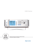


![G2 Decoder [obsolete] Second Generation User Manual](http://vs1.manualzilla.com/store/data/005963661_1-2c18e92993151caf68904a7a924089ff-150x150.png)