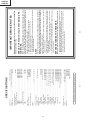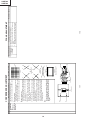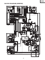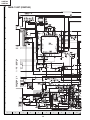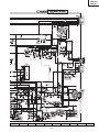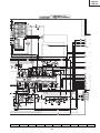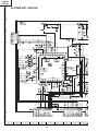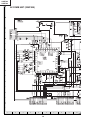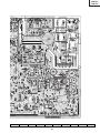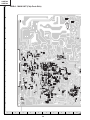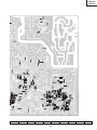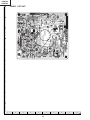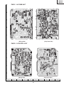
1
29WF200
29WF500
SERVICE MANUAL
S14N129WF200/0//
COLOUR TELEVISION
Chassis No. GB-1
29WF200
29WF500
MODELS
29WF200
29WF500
In the interests of user-safety (Required by safety regulations in some countries) the set should be restored
to its original condition and only parts identical to those specified should be used.
FEATURES
Ë
Ë
Ë
Ë
Ë
Ë
Ë
Ë
Ë
Ë
Ë
Ë
Ë
Ë
Ë
Ë
PAL-B/G, NTSC (AV only) (29WF200)
World Multi 28 System (29WF500)
100-CH Program Memory
AV Mode (Standard / Dynamic / Soft)
CATV Hyper Band Ready
PAL/NTSC 3 Line Comb Filter
On/Off Velocity Modulation
Black Stretch Circuit
Picture Noise Reduction
White Temp. Select
Aperture Control
Ë
Ë
Ë
Ë
Ë
S-BOOSTER
OSD-Language (English ONLY)
On/Off Reminder Timer
Power Save Mode
Rear AV-IN 1 & 2, S-Video In, AV Output (Monitor Out),
Headphone and Front AV-IN 3
3.5L Speaker Box
AFT
Component Input Terminal
AV Stereo (29WF200)
NICAM/A2 (29WF500)
CONTENTS
Page
»
»
»
»
»
»
»
»
»
»
SPECIFICATIONS ........................................... 2
IMPORTANT SERVICE NOTES ...................... 2
ADJUSTMENT PRECAUTIONS ..................... 3
TROUBLE SHOOTING FLOWCHART .......... 15
SOLID STATE DEVICE BASE DIAGRAM ..... 19
WAVEFORMS ............................................... 20
CHASSIS LAYOUT ........................................ 22
BLOCK DIAGRAM ......................................... 24
DESCRIPTION OF SCHEMATIC DIAGRAM .. 26
SCHEMATIC DIAGRAM
Ë CRT UNIT ................................................. 27
Ë MAIN UNIT ............................................... 28
Page
Ë AV COMB UNIT ........................................ 36
Ë S-CONTROL UNIT ................................... 40
Ë FRONT UNIT ............................................ 44
» PRINTED WIRING BOARD ASSEMBLIES ... 48
» REPLACEMENT PARTS LIST
Ë ELECTRICAL PARTS ............................... 56
Ë MISCELLANEOUS PARTS ...................... 66
Ë SUPPLIED ACCESSORIES ..................... 66
Ë PACKING PARTS ..................................... 66
Ë CABINET PARTS ..................................... 66
» PACKING OF THE SET ................................ 67
WARNING
The chassis in this receiver is partially hot. Use an isolation transformer between the line cord plug and power
receptacle, when servicing this chassis. To prevent electric shock, do not remove cover. No user – serviceable
parts inside. Refer servicing to qualified service personnel.
SHARP CORPORATION
1
2
2-1
Specifications are subject to change without prior notice.
Receiving Frequency
VHF ....................................................................... 44.25 MHz thru 423.25 MHz
UHF ..................................................................... 431.25 MHz thru 863.25 MHz
Dimensions ...................................................................................... Width: 800mm
Height: 583mm
Depth: 506mm
Weight(approx): 47 kg
Aerial Input Impedance
VHF/UHF .......................................................................... 75 ohms Unbalanced
Receiving Channel
PAL-B/G
VHF-Channels .............................................................................. E2 thru E12
UHF-Channels ............................................................................. E21thru E69
CATV ........................................................................ X thru Z +2, S1 thru S41
PAL-B/G, SECAM-B/G
VHF-Channels ............................................................ E2 thru E12(29WF500)
UHF-Channels .......................................................... E21 thru E69(29WF500)
CATV .................................................... X thru Z + 2, S1 thru S41 (29WF500)
PAL-D/K, SECAM-D/K
VHF-Channels ...................................... R1 thru R12, C1 thru C12(29WF500)
UHF-Channels ........................................ 21 thru 69, C21 thru C57(29WF500)
PAL-I, SECAM-I
VHF-Channels ................................................ (IRELAND) B thru J(29WF500)
UHF-Channels .......................................... (U.K.& H.K.) 21 thru 69(29WF500)
NTSC-M
VHF-Channels .......................................................... 2 thru 13(US)(29WF500)
1 thru 12 (Japan)(29WF500)
UHF-Channels ........................................................ 14 thru 69(US)(29WF500)
13 thru 62 (Japan)(29WF500)
CATV ............................................. A-6 thru A-1, A thru W+29(US)(29WF500)
C13 thru C63 (Japan)(29WF500)
Speaker
Size ..................................................................... 8 x 12 cm + 5cm round (2pcs.)
Power Input ..................................................................... 110 ~ 240V AC 50/60 Hz
Power Consumption .................................................................... 158W(29WF200)
165W(29WF500)
Audio Power Output Rating ....................................................... 10W X 2 (at Max.)
Intermediate Frequencies
Picture IF Carrier .................................................................................. 38.9MHz
Sound IF Carrier Frequency
5.5MHz ............................................................................ 33.4MHz(29WF200)
6.5MHz ............................................................................ 32.4MHz(29WF500)
6.0MHz ............................................................................ 32.9MHz(29WF500)
5.5MHz ............................................................................ 33.4MHz(29WF500)
4.5MHz ............................................................................ 34.4MHz(29WF500)
Colour Sub-Carrier Frequency
PAL .................................................................................................. 34.47MHz
NTSC ............................................................................................... 35.32MHz
Convergence ................................................................. Self Convergence System
Focus ......................................................... Bi-Potential, Uni-Potential Electrostatic
Sweep Deflection ...................................................................................... Magnetic
SPECIFICATIONS
Picture tube in this receiver employs integral implosion protection.
Replace with tube of the same type number for continued safety.
Do not lift picture tube by the neck.
Handle the picture tube only when wearing shatterproof goggles and after discharging
the high voltage completely.
2-2
1. Inspect all lead dress to make certain that leads are not pinched or that hardware is not
lodged between the chassis and other metal parts in the receiver.
2. Inspect all protective devices such as non-metallic control knobs, insulating fishpapers,
cabinet backs, adjustment and compartment covers or shields, isolation resistor- capacity networks, mechanical insulators etc.
Before returning the receiver to the user, perform the following safety Checks.
BEFORE RETURNING THE RECEIVER
1. When repairing the circuit, be sure not to increase the high voltage to more than 33.0kV
(at beam 0 µA) for the set.
2. To keep the set in a normal operation , be sure to make it function on 30.0kV ±1.5kV (at
beam 1,700 µA) in the case of the set. The set has been factory - Adjusted to the abovementioned high voltage.
∴ If there is a possibility that the high voltage fluctuates as a result of the repairs,
never forget to check for such high voltage after the work.
3. Do not substitute a picture tube with unauthorized types and/or brands which may cause
excess X-ray radiation.
This receiver is designed so that any X-Ray radiation is kept to an absolute
Minimum. Since certain malfunctions or servicing may produce potentially
hazardous radiation with prolonged exposure at close range, the followin
precautions should be observed:
X-RAY
1.
2.
3.
4.
When servicing the high voltage system, remove static charge from it by
Connecting a 10K ohm Resistor in series with an insulated wire(such as a
test probe) between picture tube dag and 2nd anode lead. (AC line cord
should be disconnected from AC outlet.)
SERVICE OF HIGH VOLTAGE SYSTEM AND PICTURE TUBE
Maintenance and repair of this receiver should be done by qualified
service personnel only.
IMPORTANT SERVICE NOTES
29WF200
29WF500
3
3-1
Precaution: If haven’t done this initialization, it may possibly generate excessive Beam current.
Note: Once the chassis has been assembly together and ready to be POWER ON for the FIRST TIME,
make sure to short JA366 & JA367 to switch to the service mode position first and then turn on the
1 above).
main power switch. (See 2-1
1 Short JA366 & JA367 and turn on the main power switch.
Initial values are automatically preset, only when a new EEPROM is used (Judge
with the first 4 bytes).
2 The initial data are preset as listed in page 5 to 8.
3 Make sure whether the data need to modification or not (Initial data).
2. Factory Presetting.
1 When the JA366 and JA367 are short-circuited, enter into the service mode.
(Adjustment through the I2C bus control).
(Use JWS Key to set as well).
2 Press the CH DOWN / UP key on the remote controller to get ready to select the
mode one by one.
3 Press the CH DOWN / UP key on the remote controller to select the modes
reversibly one by one.
4 Using the VOLUME UP/ DOWN key on the remote controller, the data can be modified.
5 When the short circuit between the JA366 and JA367 is cut off, it will be released
from the service mode.
1. Setting the service mode by the microprocessor.
This model’s setting are adjusted in two different ways: through the I2C bus control and in the
conventional analog manner. The adjustments via the I2C bus control include preset-only items
and variable data.
ADJUSTMENT PRECAUTIONS
3-2
UP
1 KEY
2 KEY
3 KEY
7 KEY
8 KEY
LATERAL MODE
(R, G, B-CUT OFF)
"_/__"
CUT OFF
BKGD
MODE
KEY
63
63 ~ 255
3 sec. TIME OUT
CUT OFF MODE
0 ~ 127
4 KEY
5 KEY
6 KEY
F/B KEY
0 KEY
63
INITIAL
DATA
DRIVE
G-DRIVE
B-DRIVE
DATA
LENGTH
DOWN
3 sec. TIME OUT
OPTION MODE 1
(refer to page 4)
MENU button
of R/C
SERVICE MODE 2
(refer to page 5)
MENU button
of R/C
MENU button
of R/C
SUB ADJ.
MODE
50Hz ADJ.
MODE
OPTION MODE 2
(refer to page 4)
60Hz ADJ.
MODE
CUT OFF
MODE
SERVICE MODE 1
R-CUT OFF
G-CUT OFF
B-CUT OFF
G-DRIVE
B-DRIVE
INITIAL
DATA
DATA
LENGTH
CUT OFF
R-CUT OFF
G-CUT OFF
B-CUT OFF
MENU button
of R/C
INFOMATION
MODE
MENU button
of R/C
(1) In the Service Mode, Key is used to select the mode in the following order.
SERVICE MODE
29WF200
29WF500
↓
(V-SIZE 50)
↓
(V-SIZE 60)
4
SUB CONT (DVD)
SUB CONT
SUB BRIGHT (DVD)
SUB BRIGHT
SECAM BELL
SECAM B-Y
SECAM R-Y
↓
↓
↓
↓
↓
↓
(SUB CONT DVD)
(SUB CONT)
(SUB BRI DVD)
(SUB BRI)
(SCM BELL)
(SCM B-Y)
(SCM R-Y)
FORWARD: CH DOWN KEY
REVERSE: CH UP KEY
(V-LINE 60)
↓
V S-CORRECTION 60Hz (V S-CORR 60)
↓
V-POSITION 60Hz
(V-CENT 60)
V-LINEARITY 60Hz
V - SIZE 60Hz
FORWARD: CH DOWN KEY
REVERSE: CH UP KEY
(V-LINE 50)
↓
V S-CORRECTION 50Hz (V S-CORR 50)
↓
V-POSITION 50Hz
(V-CENT 50)
V-LINEARITY 50Hz
V - SIZE 50Hz
FORWARD: CH DOWN KEY
REVERSE: CH UP KEY
↑
↑
↑
↑
↑
↑
SUB COLOUR (DVD)
↑
SUB COLOUR
↑
SUB TINT (DVD)
↑
SUB TINT
RF AGC
RF SUB SOUND
SUB VOLUME
PIF VCO
↑
E/W PARABOLA 60Hz
↑
H-SIZE 60Hz
↑
H-POSITION 60Hz
E/W CORNER 60Hz
TRAPEZIUM 60Hz
↑
E/W PARABOLA 50Hz
↑
H-SIZE 50Hz
↑
H-POSITION 50Hz
E/W CORNER 50Hz
TRAPEZIUM 50Hz
4-1
SUB ADJ.
MODE
60Hz ADJ.
MODE
50Hz ADJ.
MODE
(SUB TINT)
(SUB TINT DVD)
(SUB COL)
(SUB COL DVD)
(RF AGC)
(RF S-SOUND)
(SUB VOL)
(PIF VCO)
(H-CENT 60)
(H-SIZE 60)
(E/W PARA 60)
(E/W COR 60)
(TRAPE 60)
(H-CENT 50)
(H-SIZE 50)
(E/W PARA 50)
(E/W COR 50)
(TRAPE 50)
OSD
WT
S-BOOST
PIF
S/I
F-ID
TEXT
NICAM
A2
MONO-BIL
SECAM
RF NTSC
S-SYS
ROTATION
S SPD
H MODE
H POSITION
H VOLUME
LANGUAGE
COMB
AI
No.
1
2
3
4
5
6
7
8
9
10
11
12
13
14
15
16
17
18
19
20
Option setting data
4-2
SETTING DATA
29WF200
29WF500
HIGH
HIGH
ON
ON
38.9MHZ
38.9MHz
SPRIT
SPRIT
OFF
OFF
OFF
OFF
OFF
ON
OFF
ON
OFF
OFF
OFF
ON
OFF
ON
BG
BG I DK M
OFF
OFF
550kHz
550kHz
OFF
OFF
0
0
0
0
E
E
ON
ON
ON
ON
No. SERVICE MODE
EEPROM ITEM
OSD
DATA
INITIAL DATA
1 OPTION MODE 1
WHITE TEMP SETTING
WT
LOW/HIGH
HIGH
2
S-BOOST OPTION
S-BOOST
OFF/ON
ON
3
PIF FREQ. SETTING
PIF
33.50MHz ~ 58.75MHZ
38.9MHz
4
SPRIT/INTER CARRIER
S/I
SPRIT/INTER
SPRIT
5
FORCED COLOUR KILLER
F-ID
OFF/ON
OFF
6
TEXT OPTION
TEXT
OFF/ON
OFF
7
NICAM OPTION
NICAM
OFF/ON
OFF
8
A2 STEREO OPTION
A2
OFF/ON
OFF
9
MONO BILINGUAL OPTION MONO-BIL
OFF/ON
OFF
10 OPTION MODE 1
SECAM OPTION
SECAM
OFF/ON
ON
11
RF-NTSC OPTION
RF NTSC
OFF/ON
ON
12
SOUND SYSTEM SETTING
S-SYS
BG / I / DK / M
BG I DK M
13
ROTATION OPTION
ROTATION
OFF/ON
OFF
14
SERCH SPEED SETTING
S SPD
350kHz / 450kHz / 550kHz
450kHz
15
HOTEL MODE OPTION
H MODE
OFF/ON
OFF
16
HOTEL MODE POSITION H POSITION
0 ~ 99 / —
0
17
HOTEL MODE VOLUME
H VOLUME
0 ~ 60
0
18
OSD LANGUAGE
LANGUAGE
E/C/F/R/M/A
ECFRMA
19
COMB
COMB
OFF/ON
ON
20
AI
AI
OFF/ON
ON
USER DATA IN SERVICE MODE OPTION
• While SERVICE MODE 1 on, EEPROM DATA will switch to the service data.
Also, once press the menu button at the remote controller, EEPROM will switch to SERVICE MODE OPTION.
Once press the menu button again at the remote controller, EEPROM will switch back to SERVICE MODE 1.
• In the service option the user data establish as below,
Service Mode Option MENU
29WF200
29WF500
5
IC
1 CHIP
1 CHIP
1 CHIP
1 CHIP
1 CHIP
1 CHIP
1 CHIP
1 CHIP
1 CHIP
1 CHIP
1 CHIP
1 CHIP
1 CHIP
1 CHIP
1 CHIP
1 CHIP
1 CHIP
1 CHIP
1 CHIP
1 CHIP
1 CHIP
1 CHIP
1 CHIP
1 CHIP
SOUND
1 CHIP
1 CHIP
1 CHIP
1 CHIP
1 CHIP
1 CHIP
1 CHIP
1 CHIP
1 CHIP
1 CHIP
1 CHIP
1 CHIP
OSD
CUTOFF BKGD
CUTOFF DVD BKGD
V-SIZE 50
V-LINE 50
V S-CORR 50
V-CENT 50
H-CENT 50
H-SIZE 50
E/W PAR 50
E/W COR 50
TRAPE 50
SCM R-Y
SCM B-Y
SCM BELL
SUB BRI
SUB BRI DVD
SUB CONT
SUB CONT DVD
SUB TINT
SUB TINT DVD
SUB COL
SUB COL DVD
RF AGC
RF S-SOUND
SUB VOL
PIFVCO
V-SIZE 60
V-LINE 60
V S-CORR 60
V-CENT 60
H-CENT 60
H-SIZE 60
E/W PAR 60
E/W COR 60
TRAPE 60
V-ENT
H-ENT
CUTOFF/DRIVE
CUTOFF/DRIVE
V-SIZE
V-LINEARITY
V S-CORRECTION
V-POSITION
H-P0SITION
H-SIZE
E/W PARABORA
E/W CORNER
E/W TRAPEZIUM
SECAM R-Y
SECAM B-Y
BELL F0
BRIGHTNESS
BRIGHTNESS
SUB CONTRAST
SUB CONTRAST
TINT
BB-TINT
COLOUR
COLOUR
RF AGC
IF AUDIO ATT
VOLUME
#4
V-SIZE
V-LINEARITY
V S-CORRECTION
V-POSITION
H-POSITION
H-SIZE
E/W PARABORA
E/W CORNER
E/W TRAPEZIUM
V-ENT
H-ENT
3AH
76H
3BH
76H
DATA SETTING
INITIAL SETTING
DATA
DATA
#2
—
#2
—
7
22
3
3
5
4
3
4
11
8
31
50
31
35
8
7
5
17
8
8
8
8
0
0
80
80
80
80
8
4
8
4
64
64
16
16
45
45
45
70
46
34
96
95
60
255
7
26
3
3
5
6
3
2
11
10
31
50
31
32
8
5
5
17
6
6
5
5
5-1
OFFSET VALUE FROM 50Hz ADJ.
+3
+1
+1
-1
+3
0
+1
0
0
R CUT (63 ~ 255), G CUT (63 ~ 255), B CUT (63 ~ 255), G DRV (0 ~ 127), B DRV (0 ~ 127)
R CUT (63), G CUT (63), B CUT (63), G DRV (63), B DRV (63)
WHILE ADJUSTING SECAM R-Y, SECAM B-Y AND SUB-TINT, Y-MUTE OF 1 CHIP IS SET TO ON.
WHILE CHOOSING PIFVCO MODE, RF AGC SET TO "0 0" AND PIFVCO IS SET TO "1".
ADJUSTMENT FOR 60Hz. IS CHANGE AUTOMATICALLY BY 50Hz. ADJUSTMENT AS BELOW.
60Hz. ADJ.
V-SIZE (60Hz)
V-LINEARITY (60Hz)
VS-CORRECTION (60Hz)
V-POSITION (60Hz)
H-POSITION (60Hz)
H-SIZE (60Hz)
E/W-PARABOLA (60Hz)
E/W-CORNER (60Hz)
TRAPEZIUM (60Hz)
#1
#2
#3
#4
#5
EEPROM SETTING
DATA
LENGTH
1 CUT OFF
#1
2 CUT OFF (DVD)
#1
3 V-SIZE (50Hz)
0 ~ 63
4 V-LINEARITY (50Hz)
0 ~ 15
5 VS-CORRECTION (50Hz)
0 ~ 15
6 V-POSITION (50Hz)
0~7
7 H-POSITION (50Hz)
0 ~ 31
8 H-SIZE (50Hz)
0 ~ 63
9 E/W-PARABOLA (50Hz) 0 ~ 63
10 E/W CORNER (50Hz)
0 ~ 15
11 E/W TRAPEZIUM (50Hz)
0 ~ 31
12 SECAM R-Y #3
0 ~ 15
13 SECAM B-Y #3
0 ~ 15
14 SECAM BELL
0~1
15 SUB BRIGHT
0 ~ 127
16 SUB BRIGHT (DVD)
0 ~ 127
17 SUB CONT
0 ~ 15
18 SUB CONT (DVD)
0 ~ 15
19 SUB TINT #3
0 ~ 127
20 SUB TINT (DVD) #3
0 ~ 31
21 SUB COLOUR
0 ~ 127
22 SUB COLOUR (DVD)
0 ~ 127
23 RF AGC
0 ~ 63
24 RF SUB SOUND
0 ~ 127
25 SUB VOLUME
0 ~ 255
26 PIF VCO
#4
27 V-SIZE (60Hz)#5
0 ~ 63
28 V-LINEARITY (60Hz)#5
0 ~ 15
29 VS-CORRECTION (60Hz)#5
0 ~ 15
30 V-POSITION (60Hz)#5
0~7
31 H-POSITION (60Hz)#5
0 ~ 31
32 H-SIZE (60Hz)#5
0 ~ 63
33 E/W PARABOLA (60Hz)#5
0 ~ 63
34 E/W CORNER (60Hz)#5
0 ~ 15
35 TRAPEZIUM (60Hz)#5
0 ~ 31
36 V-ENT
0~7
37 H-ENT
0~7
No.
1. SERVICE MODE 1.
00H
01H
02H
03H
AFTER SHORT JA 366 & JA 367, AND TURN ON THE MAIN POWER SWITCH, READ DATA
FROM EEPROM ADDRESS 00H ~ 03H, AND COMPARE TO THE LIST BELOW, IF
ADDRESS
DATA
DIFFERENT, INITIALIZE THE EEPROM.
EEPROM SETTING
WHITE PEEK CONTROL
SUB CONTRAST
NTSC PHASE
SUB SHARPNESS (TV)
SUB SHARPNESS (AV)
SUB SHARPNESS (DVD)
RGB CONTRAST
Y-DL (B/G B/W)
Y-DL (B/G PAL)
Y-DL (B/G SECAM)
Y-DL (B/G N443)
Y-DL (B/G N358)
Y-DL (I B/W)
Y-DL (I PAL)
Y-DL (I SECAM)
Y-DL (I N443)
Y-DL (I N358)
Y-DL (D/K B/W)
Y-DL (D/K PAL)
Y-DL (D/K SECAM)
Y-DL (DK N443)
Y-DL (DK N358)
Y-DL (M B/W)
Y-DL (M PAL)
Y-DL (M SECAM)
Y-DL (M N443)
Y-DL (M N358)
Y-DL (AV B/W)
Y-DL (AV PAL)
Y-DL (AV SECAM)
Y-DL (AV N443)
Y-DL (AV N358)
SECAM GP-PHASE
SECAM ID-SENS
SECAM ID-MODE
P/N-ID
6.5M SIF FIX
DC RESTORATION
BLACK STRETCH
ABL START POINT
ABL GAIN
COLOUR GAMMA
V RAMP REF. VOLTAGE
VSM PHASE
AUDIO ATT
DATAILS CORING
DATAILS DIFF FREQ.
DATAILS GAIN
No.
1
2
3
4
5
6
7
8
9
10
11
12
13
14
15
16
17
18
19
20
21
22
23
24
25
26
27
28
29
30
31
32
33
34
35
36
37
38
39
40
41
42
43
44
45
46
47
48
2. SERVICE MODE 2.
0~1
0 ~ 127
0~3
0 ~ 63
0 ~ 63
0 ~ 63
0 ~ 63
0~3
0~3
0~3
0~3
0~3
0~3
0~3
0~3
0~3
0~3
0~3
0~3
0~3
0~3
0~3
0~3
0~3
0~3
0~3
0~3
0~3
0~3
0~3
0~3
0~3
0~3
0~1
0~1
0~1
0~1
0~3
0~3
0~3
0~3
0~1
0~1
0~1
0 ~ 127
0 ~ 63
0~1
0~7
DATA
LENGTH
5-2
WPS
S CONT
N-P NT
S SHARP T
S SHARP A
S SHARP D
RGB CONT
YBB
YBP
YBS
Y B N4
Y B N3
YIB
YIP
YIS
Y I N4
Y I N3
Y DK B
Y DK P
Y DK S
Y DK N4
Y DK N3
YMB
YMP
YMS
Y M N4
Y M N3
YAB
YAP
YAS
Y A N4
Y A N3
S G-PHASE
S ID-SENS
S ID-MODE
PN ID
6.5M
DC REST
S ST
ABL ST
ABL GA
COL G
V RAMP
VSM PHASE
ATT
WECOR
DCNG
SPAL
OSD
DATA SETTING
1 CHIP
WPS
1 CHIP
CONTRAST
1 CHIP
N PHASE
1 CHIP
SHARPNESS
1 CHIP
SHARPNESS
1 CHIP
SHARPNESS
1 CHIP
RGB CONTRAST
1 CHIP
Y-DL
1 CHIP
Y-DL
1 CHIP
Y-DL
1 CHIP
Y-DL
1 CHIP
Y-DL
1 CHIP
Y-DL
1 CHIP
Y-DL
1 CHIP
Y-DL
1 CHIP
Y-DL
1 CHIP
Y-DL
1 CHIP
Y-DL
1 CHIP
Y-DL
1 CHIP
Y-DL
1 CHIP
Y-DL
1 CHIP
Y-DL
1 CHIP
Y-DL
1 CHIP
Y-DL
1 CHIP
Y-DL
1 CHIP
Y-DL
1 CHIP
Y-DL
1 CHIP
Y-DL
1 CHIP
Y-DL
1 CHIP
Y-DL
1 CHIP
Y-DL
1 CHIP
Y-DL
1 CHIP
S GP-PHASE
1 CHIP
S ID-SENS
1 CHIP
S ID-MODE
1 CHIP
P/N-ID
1 CHIP
6.5M S-FIX
1 CHIP
DC RESTORATION
1 CHIP
BLACK STRETCH
1 CHIP
ABL START POINT
1 CHIP
ABL GAIN
1 CHIP
COLOUR GAMMA
1 CHIP
V RAMP
1 CHIP
VSM PHASE
1 CHIP
IF AUDIO ATT
COMB/AI WECOR
COMB/AI DCNG
COMB/AI SPAL
IC
When hotel mode is ON;
— Maximum volume data is determined by option setting H VOLUME.
— Channel position after POWER ON is determined by option setting H POSITION
(if option setting HOTEL-POS is not set, processing is according to last position data).
— PRESET mode is disabled.
— CH SETTING menu is not available.
HOTEL MODE
1
127
0
10
10
10
32
0
1
0
0
0
0
3
0
0
0
0
3
3
0
0
0
0
0
1
1
0
0
0
0
0
1
0
0
0
0
3
1
3
2
1
1
0
0
32
1
6
INITIAL
DATA
1
127
0
10
10
10
42
0
0
0
0
0
0
3
0
0
0
0
0
0
0
0
0
0
0
1
0
0
0
0
0
0
1
0
0
0
0
3
2
2
2
1
1
0
0
5
1
2
SETTING
DATA
29WF200
29WF500
49
50
51
52
53
54
55
56
57
58
59
60
61
62
63
64
65
66
67
68
69
70
71
72
73
74
75
76
77
78
79
80
81
82
83
84
85
86
87
88
89
90
91
92
93
94
95
96
97
98
99
100
101
102
103
104
No.
DATA
LENGTH
DATAILS LIMIT
0 ~ 15
OUTLINE DFF FREQ.
0~1
OUTLINE CORING
0~7
OUTLINE CORRECTION
0 ~ 15
DATAILS OUTLINE
0 ~ 255
YNR CORING
0~7
CHROMA BPF TV
0~3
CHROMA BPF AV
0~3
Y-DELAY TV
0~7
Y-DELAY AV
0~7
V OUTLINE LIMIT
0 ~ 15
V OUTLINE CORING
0 ~ 15
V OUTLINE DETECT
0~1
YNR DETECT GAIN
0~3
YNR CORING
0 ~ 15
B-STRETCH REFLECT
0~3
B-STRETCH THRE
0 ~63
PEDESTAIL CORRECTION
0~7
B-STRETCH INITIAL
0 ~ 31
AI ON/OFF
0~1
HISTGRAM LIMIT
0 ~ 63
Y-MIN DETECT GAIN
0~3
Y-MIN LIMIT
0 ~ 63
BASE AMOUNT
0 ~15
Y-MIN DETECT OFFSET
0 ~15
APL LAST GAIN
0~1
APL LIMIT LAST GAIN
0 ~ 63
APL SWITCH LAST GAIN 0 ~ 127
LOW APL COL LEVEL
0 ~ 63
LOW APL COL GAIN
0~3
HIGH APL COL LEVEL
0 ~ 63
HIGH APL COL GAIN
0~3
PRESCALE SCART
0 ~ 127
PRESCALE FM/AM
0 ~ 127
PRESCALE NICAM
0 ~ 127
AUTO VOLUME CORR
0~3
VOLUME NICAM BG
0 ~ 127
VOLUME NICAM I
0 ~ 127
VOLUME NICAM DK
0 ~ 127
VOLUME IGR BG
0 ~ 127
VOLUME FM
0 ~ 127
OSD H-POSITION
0 ~ 127
TEXT H-POSITION
0 ~ 127
TEXT V-POSITION
0 ~ 63
VSM GAIN(AVM1)
0~7
GAMMA POINT(AVM1)
0~3
TREBLE(AVM1)
0 ~ 60
BASS(AVM1)
0 ~ 60
SURR EFECT(AVM1)
0 ~ 15
SURR LOOP(AVM1)
0~1
VSM GAIN(AVM2)
0~7
GAMMA POINT(AVM2)
0~3
TREBLE(AVM2)
0 ~ 60
BASS(AVM2)
0 ~ 60
SURR EFECT(AVM2)
0 ~ 15
SURR LOOP(AVM2)
0~1
EEPROM SETTING
PKLM
YDO
RCOR
RMY
GAINA
BLC
BPS T
BPS A
YDL T
YDL A
VPL
KOA
YHO
YNG
COR
APSL
APMN
PHD
APA
AION
LMT
MNSL
MINLT
BSE
MNOFT
APGA
APLT
APDT
APC
CAS
APU
CUS
PRE S
PRE F
PRE N
AVC
BG L
IL
DK L
IGR L
FML
OSD-H
TEXT-H
TEXT-L
VG1SP1
G-POINT1
TRE1SP1
BASS1SP1
EF1SP1
LO1SP1
VG1SP2
G-POINT2
TRE2SP1
BASS2SP1
EF2SP1
LO2SP1
OSD
6-1
COMB/AI
COMB/AI
COMB/AI
COMB/AI
COMB/AI
COMB/AI
COMB/AI
COMB/AI
COMB/AI
COMB/AI
COMB/AI
COMB/AI
COMB/AI
COMB/AI
COMB/AI
COMB/AI
COMB/AI
COMB/AI
COMB/AI
COMB/AI
COMB/AI
COMB/AI
COMB/AI
COMB/AI
COMB/AI
COMB/AI
COMB/AI
COMB/AI
COMB/AI
COMB/AI
COMB/AI
COMB/AI
NICAM
NICAM
NICAM
NICAM
NICAM
NICAM
NICAM
NICAM
NICAM
1 CHIP
1 CHIP
SOUND
SOUND
SOUND
SOUND
1 CHIP
1 CHIP
SOUND
SOUND
SOUND
SOUND
IC
PKLM
YDO
RCOR
RMY
GAINA
BLC
BPS T
BPS A
YDL T
YDL A
VPL
KOA
YHO
YNG
COR
APSL
APMN
PHD
APA
AION
LMT
MNSL
MINLT
BSE
MNOFT
APGA
APLT
APDT
APC
CAS
APU
CUS
PRESCALE
PRESCALE
PRESCALE
PRESCALE
VOLUME
VOLUME
VOLUME
VOLUME
VOLUME
VSM GAIN
GAMMA POINT
TREBLE
BASS
SURR LEVEL
LOOP
VSM GAIN
GAMMA POINT
TREBLE
BASS
SURR LEVEL
LOOP
DATA SETTING
INITIAL
DATA
8
0
5
14
64
4
0
0
4
3
8
2
1
2
8
1
20
6
6
0
12
2
32
15
6
1
10
37
28
0
54
2
24
10
63
0
127
127
127
127
127
26
34
35
3
3
25
25
15
0
5
2
30
32
15
0
SETTING
DATA
4
1
4
14
90
0
3
0
4
3
8
7
1
0
1
1
20
6
4
1
15
1
32
15
9
1
32
10
10
2
5
2
24
10
24
0
113
103
95
125
125
25
10
37
7
2
31
28
10
0
4
2
30
30
10
0
105
106
107
108
109
110
111
112
113
114
115
116
117
118
119
120
121
122
No.
VSM GAIN(AVM3)
GAMMA POINT(AVM3)
TREBLE(AVM3)
BASS(AVM3)
SURR EFECT(AVM3)
SURR LOOP(AVM3)
S-BOOST MER
S-BOOST MEL1
S-BOOST MEL2
S-BOOST MEL3
S-BOOST MEL4
S-BOOST MEL5
S-BOOST MEL6
S-BOOST START POINT
S-BOOST STOP POINT
SIBOOST STEP POINT
AUDIO AGC
NICAM FM
EEPROM SETTING
DATA
LENGTH
0~7
0~3
0 ~ 60
0 ~ 60
0 ~ 15
0~1
0 ~ 255
0 ~ 255
0 ~ 255
0 ~ 255
0 ~ 255
0 ~ 255
0 ~ 255
0 ~ 255
0 ~ 255
0 ~ 255
0~1
0 ~ 255
VG1SP3
G-POINT3
TRE3SP1
BASS3SP1
EF3SP1
LO3SP1
MER
MEL1
MEL2
MEL3
MEL4
MEL5
MEL6
SSTP
SSPP
SSTEP
SUR AGC
NICAM FM
OSD
6-2
1 CHIP
1 CHIP
SOUND
SOUND
SOUND
SOUND
SOUND
SOUND
IC
VSM GAIN
GAMMA POINT
TREBLE
BASS
SURR LEVEL
LOOP
AGC
NICAM
DATA SETTING
INITIAL
DATA
7
1
35
35
15
0
127
180
195
210
225
240
255
25
45
5
1
80
SETTING
DATA
7
2
32
30
10
0
80
150
156
163
165
170
180
21
60
7
1
80
29WF200
29WF500
6
R/C CODE
TV-CH.
0
1
2
3
4
5
6
7
8
9
10
11
12
13
14
15
16
17
18
19
20
21
22
23
24
25
26
27
28
29
30
31
32
33
34
35
36
37
38
39
40
41
42
43
44
45
46
47
48
49
50
51
SREC/SRAC/SYI
MCL 1 (R/C CODE 117h)
CH-No.
Fv (MHz)
S-SYSTEM
SKIP OFF FREE
E-2
48.25
5.5
B/G
E-4/B-3
62.25
5.5
B/G
OIR-3
77.25
6.5
D/K
E-5
175.25
5.5
B/G
E-6/B-5
182.25
5.5
B/G
OIR-7
183.25
6.5
D/K
OIR-8
191.25
6.5
D/K
E-8/B-7
196.25
5.5
B/G
J-9
199.25
4.5
M
E-10/B-9
210.25
5.5
B/G
E-12/B-11
224.25
5.5
B/G
E-21
471.25
5.5
B/G
I-23
487.25
6.0
I
E-25
503.25
5.5
B/G
E-34
575.25
5.5
B/G
E-35
583.25
5.5
B/G
E-37
599.25
5.5
B/G
J-38
621.25
4.5
M
OIR-42
639.25
6.5
D/K
B-50
703.25
5.5
B/G
I-54
735.25
6.0
I
E-58
767.25
5.5
B/G
E-64
815.25
5.5
B/G
I-69
855.25
6.0
I
E-69
855.25
5.5
B/G
US-2
55.25
4.5
M
A-6
83.25
4.5
M
JA-6
183.25
4.5
M
JA-8
193.25
4.5
M
JA-12
217.25
4.5
M
US-14
471.25
4.5
M
JA-14
477.25
4.5
M
JA-50
693.25
4.5
M
US-83
885.25
4.5
M
S-2
112.25
5.5
B/G
S-10
168.25
5.5
B/G
SKIP OFF FREE
S-20
294.25
5.5
B/G
S-41
463.25
5.5
B/G
SKIP OFF FREE
B-43
647.25
5.5
B/G
B-45
663.25
5.5
B/G
B-47
679.25
5.5
B/G
E-5
174.95
5.5
B/G
E-5
175.55
5.5
B/G
SKIP OFF FREE
SKIP OFF FREE
SKIP OFF FREE
SKIP OFF FREE
SKIP OFF FREE
SKIP OFF FREE
7-1
SREC-SCA
MCL 2 (R/C CODE 169h)
CH-No. Fv (MHz)
S-SYSTEM
590.25
5.5
B/G
AU-0
46.25
5.5
B/G
AU-2
64.25
5.5
B/G
AU-3
86.25
5.5
B/G
AU-4
95.25
5.5
B/G
AU-5A
138.25
5.5
B/G
AU-6
175.25
5.5
B/G
AU-7
182.25
5.5
B/G
AU-8
189.25
5.5
B/G
AU-9
196.25
5.5
B/G
AU-10
209.25
5.5
B/G
AU-11
216.25
5.5
B/G
SKIP OFF FREE
SKIP OFF FREE
SKIP OFF FREE
SKIP OFF FREE
SKIP OFF FREE
SKIP OFF FREE
SKIP OFF FREE
SKIP OFF FREE
SKIP OFF FREE
SKIP OFF FREE
SKIP OFF FREE
SKIP OFF FREE
SKIP OFF FREE
SKIP OFF FREE
SKIP OFF FREE
SKIP OFF FREE
WE-28
527.25
5.5
B/G
SKIP OFF FREE
SKIP OFF FREE
SKIP OFF FREE
SKIP OFF FREE
SKIP OFF FREE
SKIP OFF FREE
SKIP OFF FREE
SKIP OFF FREE
AU-37
590.25
5.5
B/G
SKIP OFF FREE
SKIP OFF FREE
SKIP OFF FREE
E-2
48.25
5.5
B/G
WE-4
62.25
5.5
B/G
OI-3
77.25
6.5
D/K
E-5
175.25
5.5
B/G
OIR-7
183.25
6.5
D/K
OIR-8
191.25
6.5
D/K
E-10
210.25
5.5
B/G
E-12
224.25
5.5
B/G
I-23
487.25
6.0
I
WE-25
503.25
5.5
B/G
E-34
575.25
5.5
B/G
SKIP OFF FREE
99
SREC/SRAC/SYI
MCL 1 (R/C CODE 117h)
CH-No.
Fv (MHz)
S-SYSTEM
SKIP OFF FREE
SKIP OFF FREE
SKIP OFF FREE
SKIP OFF FREE
SKIP OFF FREE
SKIP OFF FREE
SKIP OFF FREE
SKIP OFF FREE
SKIP OFF FREE
SKIP OFF FREE
SKIP OFF FREE
SKIP OFF FREE
SKIP OFF FREE
SKIP OFF FREE
SKIP OFF FREE
SKIP OFF FREE
SKIP OFF FREE
SKIP OFF FREE
SKIP OFF FREE
~
R/C CODE
TV-CH.
52
53
54
55
56
57
58
59
60
61
62
63
64
65
66
67
68
69
70
~
INITIAL SETTING
7-2
SREC-SCA
MCL 2 (R/C CODE 169h)
CH-No. Fv (MHz)
S-SYSTEM
E-37
599.25
5.5
B/G
JPN-38
621.25
4.5
M
OI-42
639.25
6.5
D/K
I-54
735.25
6.0
I
E-58
767.25
5.5
B/G
WE-64
815.25
5.5
B/G
I-69
855.25
6.0
I
JA-1
91.25
4.5
M
JA-6
183.25
4.5
M
JA-8
193.25
4.5
M
JA-12
217.25
4.5
M
US-14
471.25
4.5
M
JA-50
693.25
4.5
M
S-2
112.25
5.5
B/G
S-10
168.25
5.5
B/G
S-20
294.25
5.5
B/G
S-41
463.25
5.5
B/G
E-5
174.95
5.5
B/G
E-5
175.55
5.5
B/G
SKIP OFF FREE
~
(1) Execute MCL 1/2 key to set the following data in EEPROM.
29WF200
29WF500
7
8
1
SOFT
50
-5
0
0
-5
ON
0
OFF
#
#
OFF
# SERVICE MODE DATA
CONTRAST
COLOUR
BRIGHT
TINT
SHARPNESS
PEICTURE NR
WHITE TEMP
SURROUND
TREBLE
BASS
S-BOOSTER
MODE
(2) Normal setting for AV MODE.
DATA
SETTING
LAST POWER
ON
LAST TV/AV MODE
TV
LAST CH
CH1
FLASH BACK
CH1
FAVORITE CH1
CH10
FAVORITE CH2
CH20
FAVORITE CH3
CH30
FAVORITE CH4
CH40
1 DIGIT/2 DIGIT
2 DIGIT
VOLUME
0
ROTATION
0
SAVE
OFF
AV MODE
2
BALANCE
0
BLUE BACK
OFF
ITEM
2
STANDARD
60
0
0
0
0
OFF
0
OFF
#
#
ON
8-1
3
DYNAMIC
60
10
0
0
5
OFF
0
ON
#
#
ON
DATA SETTING
VM
ON
TEXT
1
ON TIMER
IN ACTIVE
ON TIMER CH
IN ACTIVE
ON TIMER VOLUME
IN ACTIVE
REMINDER
IN ACTIVE
AFT
ALL CH ON
COLOUR SYSTEM
ALL CH AUTO
SKIP
ALL CH OFF
NICAM ON/OFF
ALL CH ON
NICAM STEREO MODE ALL CH STEREO
NICAM BILINGUAL MODE ALL CH M1
A2 ON/OFF
ALL CH ON
A2 STEREO MODE
ALL CH STEREO
A2 BILINGUAL MODE ALL CH MAIN
ITEM
(1) The following default data has been factory-setting for the EEPROM.
FACTORY-SET9
R/C
238 (Eeh)
S-SYSTEM
B/G
LANGUAGE SELECT
ENGLISH
SHIPPING SETTING & CHECKING
2
1
RF-AGC
TAKE OVER
POINT ADJUSTMENT
(I2C BUS
CONTROL)
TUNER IFT
( PRESET )
TU200
No. Adjusting point
Oscilloscope
P
Fig.2
1000p
IF OUT
-1.5+/-0.8dB
C
1000p 75ohm
1n60
E-9 CH
Fig.1
100k
10k
Waveform or others
8-2
» Bias box: About 4.5 V
Fig. 3
3. Call "RF-AGC" mode in service mode. Adjust the
"RF-AGC" bus data to obtain the Tuner output pin
drop 0.1V ~ 1.0V below maximum voltage.
4. Change the antenna input signal to 63~67dBµV,
and make sure there is no noise.
5. Turn up the input signal to 90~95 dBµV to be sure
that there is no cross modulation beat.
—
1. Receive "PAL COLOUR BAR" signal.
» Signal Strength: 54 ± 1 dBµV (75 ohm open)
Note: For the 50 W signal
strength gauge, when not using 50/75 impedance adapter,
signal strength is
2. Connect the oscilloscope to TP51 (Tuner’s AGC
Terminal) as shown in Fig. 3.
52 ±1dB µV(75 W open), instead of 54 ±1dB µV (75 W
Oscilloscope
open).
+
TP51
0.1V
Precaution: The loss of using
~1.0V —
impedance adapter.
TV Set
Bias box
+
Note: Be sure to keep the tuner cover in position
during this adjustment.
1. Get the tuner ready to receive the CH. E -9
signal,but with no signal input.
Adjust the PLL data.
2. Connect the sweep generator's output cable to the
tuner antenna. ( RF SWEEP )
3. Adjust the sweep generator's to 80dBµV.
4. Connect the response lead ( use LOW IMPEDANCE probe with wave detector ; see Fig.1 ) to the
tuner's IF output terminal. ( This terminal must
have the probe alone connected ).
5. Set the RF AGC to 0 - 6 V with no saturation with
the waveform.
6. Adjust the tuner IF coil to obtain the waveform as
shown in Fig. 2.
Adjusting condition/procedure
PIF ADJUSTMENT
29WF200
29WF500
1
PURITY ADJ.
No. Adjusting point
9
Monocolour
screen release
Monocolour
BLUE
screen
Monocolour
RED
screen
9-1
* Adjustment for uniformity is mentioned in another
content. Please refer to the following page.
Monocolour
GREEN
screen
* Every push of the monocolour key, changes the
screen as follows.
Note: Apply the adjustment after aging with
the beam current 1700 ± 50 µA or more
for 30 minutes or more.
Note: Select the service mode, and press the
monocolour key of R/C for process,and
the monocolour screen (green) will be
selected.
1. Select the green monocolour screen with remote controller, and set the beam current of
1.7mA with the contrast control.
2. Degauss the CRT enough with the degausing coil.
For the adjustable magnetic field
NOTE: Horizontal = 0
Vertical = 0.1
Adjustable magnetic field is shown in P8-1.
3. The purity magnet must be previously set at the
zero magnetic field, and the convergence must
be adjusted to be rough.
With P-MG, adjust it to the center - rank A.
4. Observe the points a, b as shown in Fig. 4-1
through the microscope.
Move DY fore and aft to set the landing at the
point. (rank A)
5. If the a/b balance is poor, compensate it to the
center "Rank AB".
6. Aline it to zero, keeping the raster rotation in the
east direction.
7. Tighten the deflection coil fastening screws.
» Tightening torque: 108 ± 20 N (11 ± 2 kgf)
8. Checking the CRT corner area, bond the magnetic sheet to set the landing at Rank A for compensation.
Adjusting condition/procedure
PURITY ADJUSTMENT
B
A
Fig. 4-1
A=B
90mm
b
A=B
* Even with TEXT key or "R/G/
Cy" key, it can be directly
switched to each monocolour
screen.
* Continuosly press the monocolour key 1 second or more,
and the monocolour mode will
be selected without the service
mode.
Rank "A"
(on the left of CRT)
Fig. 4-3
B
A
Fig. 4-2
Rank "A"
(on the right of CRT)
90mm
a
Waveform or others
2
Uniformity
adjustment (To
perform after
the purity and
convergence
adjustment.)
No. Adjusting point
9-2
* During the pasting of compensation magnet, use
the crosshatch pattern.
Make sure there is no blur or bend lines occur.
If the blur or bend are serious, adjust the location
of compensation magnet to make it better.
(The same method is applied for adjustment of
monocolour screen Blue for blue uniformity, and
changing both the magnetic field for North and South
direction.)
(South direction Red uniformity)
1. Horizontal mf = Set to monocolour screen Red
and adjust to - 0.25G.
2. Pay attention to the edge of CRT, if the landing is
poor, adjust by attaching the compensation magnet at the back of the CRT.
(North direction Red uniformity)
1. Horizontal mf = Set to monocolour screen Red
and adjust to + 0.25G.
2. Pay attention to the edge of CRT, if the landing is
poor, adjust by attaching the compensation magnet at the back of the CRT. (Refer to Fig.5)
Before adjustment begin,
Horizontal magnetic field = 0G
Vertical magnetic field = Each destination's adjustment magnetic field.
Make sure degauss it.
Adjusting condition/procedure
(CRT back)
Fig. 5
Compensation magnet
(CRT surface)
Miss landing
Waveform or others
PURITY ADJUSTMENT (Continued)
29WF200
29WF500
1
CONVERGENCE
ADJ.
( To be done
after the purity
adjustment.)
No. Adjusting point
10
YH
YHC
10-1
Balance Coil
B
B
Purity Magnet
R
R
4-Pole Magnet
Lacquer
B
B
B
X axis
25mm ± 0.5mm
CRT NECK
Fig. 6-4
Adjust by Swing DY
Fig. 6-3
Adjust by Balance Coil
Fig. 6-2
Adjust by YH
R
Fig. 6-1
Adjust by YHC
R
Y axis
Waveform or others
6-Pole Magnet.
Note:
In case of poor convergence adjustment on
the top and bottom of the screen, adjust DY
by swing rightward and leftward. (Refer to
Fig.6-4.)
Dynamic convergence
1. Fix the wedges in a position so that the deflection
york neck is at the center of top bottom and left
right. (Straight line and without any blur horizontal / vertical line.)
2. Adjust the Red, Blue, upper and lower of the
center Y axis on the screen by using the
Volume(YH, YHC) at the deflection york. (Refer
to Fig.6-1 and 6-2.)
3. If the Horizontal Red, Blue (XV) on the screen
center X axis is shifted, correct the Red. Blue (XV)
by adjusting the balance coil on the deflection
york. (Refer to Fig.6-3.)
4. After confirm that there is no problems on the
entire screen, bond each wedge on CRT and glass
tape on it. Fastening the screws of DY and magnet unit (purity, 4-pole and 6-pole), then coat the
lacquer paint on DY fastening screw and magnet
unit fastening screw.
Static convergence
1. Overlap blue and red with the open-/closing angle and rotation of the 4 pole magnet.
2. Overlap green on blue and red with the open-/
closing angle and rotation of the 6 pole magnet.
1. Receive the "Crosshatch Pattern" signal.
2. Using the remote controller, call NORMAL mode.
Adjusting condition/procedure
CONVERGENCE ADJUSTMENT
1
FOCUS ADJUSTMENT
No. Adjusting point
10-2
1. Receive E-5CH (Monoscope Pattern).
2. With the remote controller, make the image
normal.
3. Adjust the focus VR to make the character "575"
on left bottom of monoscope as fine as possible.
Adjusting condition/procedure
FOCUS ADJUSTMENT
Waveform or others
29WF200
29WF500
11
WHITE BALANCE BACKGROUND I2C
BUS ADJUSTMENT (DVD
SIGNAL)
3
11-1
1. The window pattern is received with DVD signal
(component signal).
2. Apply the adjustment in the same manners as 2
(AV-IN SIGNAL) and subsequence above. (GDRIVE, B-DRIVE, R-CUT OFF, G-CUT OFF, BCUT OFF)
Apply the adjustment after the end of 2 (AV-IN
SIGNAL).
* The colour temperature is based on the shipment
initial setting table.
1. Receive "WHITE" Pattern with COLOUR BURST
signal.
2. Select P-NORM with the remote controller.
3. Connect the beam ammeter between TP1601 and
TP1602.
4. Coarsely confirm the beam current to approx.
1.7mA.
5. Receive the window pattern with AV input.
(PAL burst is generated with the signal generator.)
6. With the data of G-drive and B-drive, adjust the
colour temperature 12,300°K of the 50% white.
7. Adjust the right dark area of the window to
17,000°K with R-cut off, G-cut off and B-cut off.
8. Read just the colour temperature at the 50%
white.
9. Check 12,300°K at the dark white.
Note1 : Apply this adjustment after aging with
the beam current 1,700±50µA or more for 30
min or more.
(On the white or green minocolour screen)
WHITE BALANCE BACKGROUND I2C
BUS ADJUSTMENT (AV-IN
SIGNAL)
2
Dark white
50% white
Note2:
Use the window pattern of the signal generator SX-1006 for
adjustment.
( PA L a n d c o l o u r b u r s t a r e
present.)
*18,000°K X : 0.255 Y : 0.255
*17,000°K X : 0.261 Y : 0.261
*12,300°K X : 0.272 Y : 0.275
(With Minolta colour thermometer
CA-100)
Note1: Data up/down is possible
with the below comparison.
R CUT OFF UP
"1"KEY
DOWN
"4"KEY
G CUT OFF UP
"2"KEY
DOWN
"5"KEY
B CUT OFF UP
"3"KEY
DOWN
"6"KEY
G-DRIVE
UP
"7"KEY
DOWN
"
"KEY
B-DRIVE
UP
"8"KEY
DOWN
"0"KEY
On the monocolour screen of white or
green.
* Befor doing adjustment, make sure the
R/G/B-cut and the B/G-Drive is at initial
value.
1. Receive "WHITE" Pattern with Colour Burst
signal.
2. Select P-NORM with the remote controller.
3. Select the CUT OFF BKGD mode at the service
mode.
4. Select the screen VR 0/10.
5. Press "-/--" key of the remote controller to select
the lateral in-line mode.
6. Turn the screen VR clockwise, and adjust the first
lighting lateral in-line raster to slighly light.
7. Adjust the CUT OFF data of two other colours,
and coarsely adjust the lateral in-line to become
white. (Note 1)
8. Turn the screen VR in the opposite direction to
the point where the lateral in-line raster goes out.
Note 1: Apply the adjustment after aging with
the beam current 1,700±50µA or more for 30
min or more.
9. Press "-/--" key of the remote controller to select
the normal mode.
CRT CUTOFF
ADJUSTMENT
(I2C BUS
CONTROL)
Waveform or others
Adjusting condition/procedure
1
No. Adjusting point
CUT-OFF, BACKGROUND AND SUB-CONTRAST ADJUSTMENT
1. Receive the window pattern with AV input.
2. Make the image normal with the remote controller.
3. Select the SUB-CONTRAST adjustment mode
with the remote controller, and adjust 50% white
to 165 ± 10cd.
SUBCONTRAST
I2C BUS
ADJUSTMENT
(AV-IN
SIGNAL)
SUBCONTRAST
I2C BUS
ADJUSTMENT
(DVD SIGNAL)
6
7
11-2
1. Select the DVD mode.
2. Receive the signal of the DVD signal generator.
(Component signal) (Window pattern)
3. Select the SUB-CONTRAST adjustment mode
(DVD) with the remote controller, and adjust 50%
white to 165 ± 10 cd.
1. Select DVD mode.
2. Receive the signal of the DVD signal generator.
(Component signal) (Window pattern)
3. Make the image normal with the remote controller.
4. Select the SUB-BRIGHT adjustment mode (DVD),
and adjust the right dark white area of the window
pattern to 2.8 ± 0.5 cd of the window pattern.
SUB-BRIGHTNESS
ADJUSTMENT
(I2C BUS
CONTROL)
(DVD SIGNAL)
5
Adjusting condition/procedure
1. Receive the window pattern with AV input.
2. Make the image normal with the remote controller.
3. Select the SUB-BRIGHT adjustment mode with
the remote controller, and adjust the right dark
white area of the window pattern to 5.5 ± 0.5 cd.
SUB-BRIGHTNESS
ADJUSTMENT
(I2C BUS
CONTROL)
(AV-IN
SIGNAL)
4
No. Adjusting point
(Continued)
Dark white
50% white
Note 3:
Use "Y" of Minolta colour
analyzer CA-100 in adjustment.
Note 4:
Use the window pattern of the
signal generator SX-1006 for adjustment.
CUT OFF POINT
Reference:
* When E-2 CH (Crosshatch pattern)
or equivalent signal is received.
1.Make the image normal with the
remote controller.
2.Adjust the 4rd (1 thru 5 from the
left) black of the window pattern to
sink.
Waveform or others
CUT-OFF, BACKGROUND AND SUB-CONTRAST ADJUSTMENT
29WF200
29WF500
1
12
Adjust the linearity to the best.(monoscope)
Already preset. (Adjust this unless the linearity is
achieved.) (monoscope)
Align the center of the screen to the geometric center
of CRT.(monoscope)
Align the center of the screen to the geometric center
of CRT.(monoscope)
Adjust the overscan to 8.5%.(monoscope)
Adjust the 2nd vertical line from the right end of the
crosshatch pattern so that the midddle 4 blocks are
straight. (Refer to Fig.7-1)(crosshatch)
Adjust the 2nd vertical line from the right end of the
crosshatch pattern so that the top are straight. (Refer
to Fig.7-2)(crosshatch)
Adjust the 2nd vertical line from the right end of the
crosshatch pattern so that the D1 (center area of the
second vertical line-edge of screen) and D2 (top area
of the second vertical line-edge of screen) are
same.(Refer to Fig.7-3)
Already preset.
Already preset.
On the items of V-AMP 60, V-LINE 60, V S-CORR
60, V-CENT 60, H-CENT 60, H-SIZE 60, E/W-PAR
60, E/W-COR 60 and TRAPE 60, the data is
automatically input if the 50Hz mode adjusutment is
done.
however, if it is largely devisted when it is check in
the 60Hz. Mode Readjust in the 60Hz. Mode.
V-LINE 50
V S-CORR 50
V-CENT 50
H-CENT 50
H-SIZE 50
E/W-PAR 50
E/W-COR 50
TRAPE 50
V-EHT
H-EHT
OTHER
12-1
Attention:
Don't change 50Hz mode data after adjust 60Hz mode
data.Because 60Hz mode data follow the 50Hz mode
data automatically.
Adjust the overscan to 8.5%.(monoscope)
Adjusting condition/procedure
V-AMP 50
MAIN SCREEN
ADJUSTMENT
No. Adjusting point
Fig. 7-3
Fig. 7-2
Fig. 7-1
Waveform or others
D1
D2
HORIZONTAL AND VERTICAL DEFLECTION LOOP ADJUSTMENT
Adjusting condition/procedure
12-2
NOTE: (Optional)
If using RF input, please refer to the Fig.
9-2 waveform.
3. Vary the sub tint data to adjust the waveform to
be gained as shown in Fig.9-1.
TP47B......(KY) 6pin
Adjusting condition/procedure
1. Select the sub-tint adjustment mode (automatic
Y cut) to receive the "NTSC Colour Bar" (AV input).
2. Connect the oscilloscope to TP47B
» Range : 20mV/Div. (AC)(Use Probe 10:1)
» Sweep time : 20 µsec/Div.
1
75% W
A
B
C
Optional
A=B=C
(B-Y)
Fig. 8-1
B
B
Fig. 9-2
W Y Cy G Mg R
RF input
Fig. 9-1
W Y Cy G Mg R
A
AV input
Waveform or others
A=B
(B-Y)
G
Y 100% W Mg
Cy
Waveform or others
NTSC CHROMA ADJUSTMENT
1. Receive "PAL Colour Bar" signal.
2. Make the image normal with the remote controller.
3. Connect the oscilloscope to IC850#9pin. (Using
10:1 Probe)
Range :
2 V/Div
Sweep Time : 20 µ sec/Div
4. Set the sub-colour adjustment mode with the
remote controller, and vary the sub colour data to
make 75% W of the colour bar and RED at the
same level for adjustment shown in Fig.8-1.
SUB-TINT
(I2C BUS
CONTROL)
SUB COLOUR
(I2C BUS
CONTROL)
PAL CHROMA ADJUSTMENT
No. Adjusting point
1
No. Adjusting point
B
B
R
29WF200
29WF500
1
Adjusting condition/procedure
13-1
SECAM BLACK 1. Receive (SECAM colour bar).
LEVEL R-Y/B-Y 2. Select SECAM black level adjustment R-Y mode.
I2C BUS AD3. Connect the oscilloscope to pin(20) of IC201(R
JUSTMENT
out).
» Range : 10mV/Div.
» Sweep time : 20 µsec/Div.(Probe 10:1 is used)
4. Vary R-Y data to minimize the offset between the
non-signal line and signal line as shown in Fig.101(b)
5. Select SECAM black level adjustment B-Y mode.
6. Reconnect the oscilloscope to 22pin of IC800 (B
Out)
The conditions are the same as in Item 3.
7. Vary B-Y data to minimize the offset between the
non-signal line and signal (TP47RB) line as shown
in Fig.10-2(b)
No. Adjusting point
13
Fig. 10-2(b)
OFF SET
Fig. 10-2(a)
Fig. 10-1(b)
Fig. 10-1(a)
OFF SET
Waveform or others
SECAM CHROMA ADJUSTMENT(29WF500 only)
WHITE TEMP
NORMAL Key
7
8
CH DISPLAY
COLOUR
6
SHARPNESS
Key
TINT key
4
5
BRIGHTNESS
key
COLOUR key
2
3
CONTRAST
key
1
No. Adjusting point
13-2
1. Receive "Monoscope Pattern" signal.
2. Set FUNCTION to select WHITE TEMP.
3. Press Volume Up/Down key to check WHITE
TEMP Option, STANDARD:
NORMAL SETTING, WARM for more REDDISH
direction changing, COOL for more BLUISH direction changing.
1. Once in PICTURE Mode, and the NORMAL key
is pressed, all the settings will be present to normal setting.
(Normal setting value for every mode, refer table
on page8-1.)
1. All Ch (1~99) will have an OSD display of the
channel number in green colour under AFT ON
condition.
1. Receive "Monoscope Pattern" signal.
2. Press to MENU mode, then Select Picture Mode
and set to select SHARPNESS.
3. Press Volume Up/Down key to check whether the
SHARPNESS effect is OK or not.
1. Receive the "NTSC Colour Bar" signal thru AV in.
2. Press to MENU mode, then Select Picture Mode
and set to selectTINT.
3. Press Volume Up/Down key to check TINT, UP
for GREEN direction and DOWN for RED direction whether is OK or not.
1. Receive "Monoscope Pattern" signal.
2. Press to MENU mode, then Select Picture Mode
and set to select BRIGHTNESS.
3. Press Volume Up/Down key to check whether the
BRIGHTNESS effect is OK or not.
1. Receive "Colour Bar" signal.
2. Press to MENU mode, then Select Picture Mode
and set to select COLOUR.
3. Press Volume Up/Down key to check whether the
COLOUR effect is OK or not.
1. Receive "Monoscope Pattern" signal.
2. Press to MENU mode, then Select Picture Mode
and set to select CONTRAST.
3. Press Volume Up/Down key to check whether the
CONTRAST effect is OK or not.
Adjusting condition/procedure
Notes:If nothing is display
mean contrast, colour, bright,
tint, sharpness are all in normal setting.
Waveform or others
FUNCTION OPERATION CHECKING (VIDEO AND AUDIO)
29WF200
29WF500
14
HEADPHONE
OUTPUT
CHECKING
NOISE MUTE
CHECKING
12
SOUND
SYSTEM
(29WF500
only)
10
11
COLOUR
SYSTEM
(29WF500
only)
9
No. Adjusting point
14-1
1. Receive "PAL COLOUR BAR" signal.
2. Turn up the volume control to maximum, make
sure the sound is beard from the speakers. Then
put the unit in no signal state.
3. Check the sound mute is effective.
4. Finally turn sound level of CTV to minimum.
(Ref: Output level of Headphone is as following
Apx. 500mVp-p)
1. Receive PAL COLOUR BAR with SOUND 400Hz,
100% MODULATION (±50kHz Dev).
2. Maximum volume, and check the headphone output with 400Hz sound and no sound out from
speaker.
1. Receive “PAL-D/K” signal, press the “SOUND
SYSTEM” to select B/G, I. Check the sound output is not working properly. Select D/K and check
the sound output to make sure it is working properly.
2. Receive “PAL-I” signal, press the “SOUND SYSTEM” to select B/G, D/K. Check the sound output
is not working properly. Select I and check the
sound output to make sure it is working properly.
3. Receive “PAL-B/G” signal, press the “SOUND
SYSTEM” to select I, D/K. Check the sound output is not working properly. Select B/G and check
the sound output to make sure it is working properly.
1. Receive the "PAL COLOUR BAR" signal, press
the COLOUR SYSTEM key to select modes except PAL, check the COLOUR is not working properly. Then, select the "PAL" mode. Check again
its colour so that it is working properly.
2. Receive "SECAM COLOUR BAR" signal, press
COLOUR SYSTEM key to select modes except
SECAM, check the COLOUR is not working properly. Then, select the "SECAM" mode. Check
again its colour so that it is working properly.
3. Receive “NTSC 4.43” signal, press COLOUR
SYSTEM key to select modes except NTSC4.43,
check the COLOUR is not working properly. Then,
select the “NTSC 4.43” mode. Check again its
colour so that it is working properly.
4. Receive “NTSC 4.43/3.58 COLOUR BAR” signal
thru AV, press COLOUR SYSTEM key to select
modes except N4.43/3.58, check the COLOUR
is not working properly. Then, select the “NTSC
4.43/3.58” mode. Check again its colour so that it
is working properly.
Adjusting condition/procedure
(Continued)
Waveform or others
FUNCTION OPERATION CHECKING (VIDEO AND AUDIO)
H•V PROTECTOR
OTHER
PROTECTORS
OUTPUT
CHECKING
1
2
14-2
* Correspondence for short circuit of smoothing
electrolysis of +B line and so on.
To check the operation of protector and so on,
take care for the breakage, deterioration and so
on of each element.
1. Receive E-5CH (Monoscope Pattern).
2. Connect the Bias Box to the cathode side (R653)
of D652.
3. Set the voltage of the Bias Box at 10V, and verify
that the protector does not operate.
4. Set the voltage of the Bias Box at 18V, and verify
that the protector operate.
Adjusting condition/procedure
Reference Approx. 12.2V as ordinary.
Waveform or others
PROTECTOR OPERATION CHECKING
No. Adjusting point
29WF200
29WF500
Check IC501 and
related circuits
Normal
Check IC201 and its
peripheral parts.
Abnormal
15-1
Check the voltage at pin (6) of IC501.
Check vertical trigger pulse at pin (26) of IC201.
Normal
NO VERTICAL SCAN
Check D501 and R501.
Abnormal
TROUBLE SHOOTING FLOWCHART
Check IC850.
Normal
Check R621,
IC201 and its
peripheral parts.
Abnormal
Check CRT connector (KY), (H) bias.
GREEN
GREEN
15
15-2
Check
protecter circuit
and its related
parts (23) pin
of IC2001
vertical pulse.
Yes
No
Check the power
circuit consisting
of IC701, Q701
IC702, IC703 and
Q602.
Does horizontal circuit
momentary oscillate?
RED
Power on by R/C.
RED
LED COLOUR ?
NO RASTER
TROUBLE SHOOTING FLOWCHART (Continued)
29WF200
29WF500
No
16
Check the
peripheral circuit
of IC701, IC702,
IC703, IC751 and
D725.
No
16-1
Check Q2003,
Q2059 and
IC2001.
Yes
Replace the Fuse.
Blown out
Check the power circuit
consisting of T702, IC701,
Q701 etc.
Yes
Is the Fuse again blown out?
Does 5V appear at pin (39) of IC2001.
Normal
Check F4701.
F3700.
NO LED LIGHT
TROUBLE SHOOTING FLOWCHART (Continued)
Check TU51.
Yes
Does 33V appear at pin (9) of
TU51.
Yes
Does 5V appear at pin (6) and (7)
of TU51 (TUNER).
Snow noise increase.
No
No
Yes
16-2
Check IC751, Q728 etc.
Check IC751.
Does the snow noise appear
on the picture tube at max
contrast and brightness
control?
NO PICTURE
No
B
TROUBLE SHOOTING FLOWCHART (Continued)
29WF200
29WF500
17
Check IC1900,
IC1901 Q1901, and
their peripheral
circuit.
No
(Noise)
Check pin (39) of
IC201 noise or signal
appear?
Yes
(Signal)
Check pin (43) of
IC1900 noise or
signal appear?
No
Is AV1, AV2, AV3 or
input normal?
Noise or signal
appear.
Normal
Yes
(Signal)
No
(Noise)
Yes
17-1
Check IC201 and
their peripheral
circuit.
No
Yes
Check IC1900 and its
peripheral circuit.
Check IC201 RGB
out Normal?
Abnormal
Check the
peripheral circuits
of screen heater
(FBT) and the CRT.
Yes
No
Check IC850 and
their peripheral
circuit.
Are pin (7), (8) and (9) of
IC850.
Check TU51(TUNER),
SF201 and its related parts.
Check Q405 and their
peripheral circuit.
Check pin (6) and (7) IC201.
No snow noise.
B
TROUBLE SHOOTING FLOWCHART (Continued)
Check
TU51
peripheral
parts.
Yes
Check TU51
and its
peripheral
circuits of no
problem, set
the sound
system
inpositon.
Yes
Check
IC1900 and
its peripheral
circuit.
No
Is there audio
signal at pins
(46), (48) of
IC1900?
No
Change the sound system.
Is sound normal?
Check TV sound.
No
17-2
Yes
Check IC4301 and
their peripheral
circuit.
Check IC1900
peripheral
parts.
No
No
Yes
Check IC361, and
their peripheral
parts.
Yes
Is there audio
signal at pin (2)
and (5) of IC361?
Check IC3501.
No
Set S-Volume at
maximum.
Do pins (5), (20)
of IC3501 work?
Yes
Is there audio signal at pins (2), (23)
of IC3501?
Is audio output terminal J901
normal.
NO NORMAL SOUND
TROUBLE SHOOTING FLOWCHART (Continued)
29WF200
29WF500
18
Check IC201 and
their peripherals.
PAL, SECAM,
NTSC4.43:
Check X800, pin
(12) of IC201 and
their peripherals.
No
Yes
Yes
No
Yes
Yes
18-1
Check IC850.
Yes
Are signal waveforms at
TP47R and TP47B proper?
Check D621
and its
peripherals.
No
Check Q1900
and their
peripherals.
No
Is chroma input level of IC201
pin (43) proper?
No
Turn on colour system forced
switch. Does colour appear?
No
Turn on colour control. Does
colour appear?
NO COLOUR
Is SCP signal waveform at pin (30) of
IC201 proper?
Fix cotrol to
coloured
system.
Set colour
control.
Check TU51, Q405,
IC1900 and their
peripherals.
Yes
Is only RF signal's colour abnormal?
NO SPECIFIC COLOUR
C
TROUBLE SHOOTING FLOWCHART (Continued)
No
White
balance:
Check RGB
output circuit
of IC201.
SET Subcolour.
Yes
Check IC201.
Yes
Yes
18-2
PAL, SECAM, NTSC4.43:
Check X800 pin (12) of IC201 and
their peripherals.
No
Check IC201
and its
peripherals.
No
Can the sub-colour be readjusted
in service mode?
Check IC201.
Turn up and down colour control.
Does colour gain go up and
down?
Yes
No
Colour control circuit detective.
Colour saturation control does not
work.
Are signal waveforms at TP47B and TP47R
proper?
APG circuit:
Check IC201
and its
peripherals.
Yes
Turn colour control to minimum.
Does colour disappear?
Colour in B/W mode.
COLOUR PRODUCED
C
No
No
Check D621 and its
peripherals.
No
Is SCP signal waveform at pin
(30) of IC201 proper?
Check pin (45) of
IC1900, IC1402, and
their peripherals.
Yes
Is chroma input level pin (43) of
IC201 proper?
Ref. value: 100 ~ 500mVp-p.
Fix control to
coloured system.
Yes
Turn on colour system forced
switch. Does colour appear?
Fix control to coloured system.
TROUBLE SHOOTING FLOWCHART (Continued)
29WF200
29WF500
29WF200
29WF500
SOLID STATE DEVICE BASE DIAGRAM
TOP VIEW
SIDE VIEW
19
29WF200
29WF500
WAVEFORMS
20
29WF200
29WF500
-MEMO-
21
29WF200
29WF500
MODEL 29WF200 CHASSIS LAYOUT
22
29WF200
29WF500
MODEL 29WF500 CHASSIS LAYOUT
23
29WF200
29WF500
BLOCK DIAGRAM (29WF200)
24
29WF200
29WF500
BLOCK DIAGRAM (29WF500)
25
29WF200
29WF500
DESCRIPTION OF SCHEMATIC DIAGRAM
SAFETY NOTES:
NOTES:
1. DISCONNECT THE AC PLUG FROM THE AC OUTLET BEFORE
REPLACING PARTS.
2. SEMICONDUCTOR HEAT SINKS SHOULD BE REGARDED AS
POTENTIAL SHOCK HAZARDS WHEN THE CHASSIS IS OPERATING.
1. The unit of resistance “ohm” is omitted.
(K = 1000 ohms, M = Meg ohm).
2. All resistors are 1/16 watt, unless otherwise noted.
3. All capacitors are µF, unless otherwise noted. (P = µµF).
VOLTAGE MEASUREMENT CONDITIONS:
IMPORTANT SAFETY NOTICE:
PARTS MARKED WITH “å” (
) ARE IMPORTANT FOR
MAINTAINING THE SAFETY OF THE SET. BE SURE TO REPLACE THESE PARTS WITH SPECIFIED ONES FOR MAINTAINING THE SAFETY AND PERFORMANCE OF THE SET.
1. Voltage in parenthesis measured with no Signal.
2. Voltages without parenthesis measured with PAL ColourSignal.
3. All the voltages in each point are measured high impedance
volt-meter.
SERVICE PRECAUTION:
WAVEFORM MEASUREMENT CONDITIONS:
THE AREA ENCLOSED BY THIS LINE (
) IS DIRECTLY
CONNECTED WITH AC MAINS VOLTAGE.
WHEN SERVICING THE AREA, CONNECT AN ISOLATING TRANSFORMER BETWEEN TV RECEIVER AND AC LINE TO ELIMINATE
HAZARD OF ELECTRIC SHOCK.
1. Colour bar generator signal of 1.8V peak to peak applied at
Base of Video Buffer Amp. Q405.
2. Approximately 4.0 V AGC bias.
26
29WF200
29WF500
SCHEMATIC DIAGRAM
CRT UNIT
J
I
H
G
F
E
D
C
B
A
1
2
3
4
5
6
27
7
8
9
10
29WF200
29WF500
MAIN-1 UNIT (29WF200)
J
I
H
G
F
E
D
C
B
A
1
2
3
4
5
6
28
7
8
9
10
29WF200
29WF500
10
11
12
13
14
15
29
16
17
18
19
29WF200
29WF500
MAIN-2 UNIT (29WF200)
J
I
H
G
F
E
D
C
B
A
1
2
3
4
5
6
30
7
8
9
10
29WF200
29WF500
10
11
12
13
14
15
31
16
17
18
19
29WF200
29WF500
MAIN-1 UNIT (29WF500)
J
I
H
G
F
E
D
C
B
A
1
2
3
4
5
6
32
7
8
9
10
29WF200
29WF500
10
11
12
13
14
15
33
16
17
18
19
29WF200
29WF500
MAIN-2 UNIT (29WF500)
J
I
H
G
F
E
D
C
B
A
1
2
3
4
5
6
34
7
8
9
10
29WF200
29WF500
10
11
12
13
14
15
35
16
17
18
19
29WF200
29WF500
AV COMB UNIT (29WF200)
J
I
H
G
F
E
D
C
B
A
1
2
3
4
5
6
36
7
8
9
10
29WF200
29WF500
10
11
12
13
14
15
37
16
17
18
19
29WF200
29WF500
AV COMB UNIT (29WF500)
J
I
H
G
F
E
D
C
B
A
1
2
3
4
5
6
38
7
8
9
10
29WF200
29WF500
10
11
12
13
14
15
39
16
17
18
19
29WF200
29WF500
S-CONTROL UNIT (29WF200)
J
I
H
G
F
E
D
C
B
A
1
2
3
4
5
6
40
7
8
9
10
29WF200
29WF500
10
11
12
13
14
15
41
16
17
18
19
29WF200
29WF500
S-CONTROL UNIT (29WF500)
J
I
H
G
F
E
D
C
B
A
1
2
3
4
5
6
42
7
8
9
10
29WF200
29WF500
10
11
12
13
14
15
43
16
17
18
19
29WF200
29WF500
FRONT UNIT (29WF200)
J
I
H
G
F
E
D
C
B
A
1
2
3
4
5
6
44
7
8
9
10
29WF200
29WF500
10
11
12
13
14
15
45
16
17
18
19
29WF200
29WF500
FRONT UNIT (29WF500)
J
I
H
G
F
E
D
C
B
A
1
2
3
4
5
6
46
7
8
9
10
29WF200
29WF500
10
11
12
13
14
15
47
16
17
18
19
29WF200
29WF500
PRINTED WIRING BOARD ASSEMBLIES
PWB-A: MAIN UNIT (Wiring Side)
J
I
H
G
F
E
D
C
B
A
1
2
3
4
5
6
48
7
8
9
10
29WF200
29WF500
10
11
12
13
14
15
49
16
17
18
19
29WF200
29WF500
PWB-A: MAIN UNIT (Chip Parts Side)
J
RJ 6 5
F DC1
R6 3 8
I
H
C6 0 5
G
R6 1 8
RJ 4 2
R6 1 7
R6 9 1
Q6 1 7
R9 2 6
C6 9 0
C9 2 1
R6 8 6
F
Q6 1 6
C9 9
RJ
52
9
RJ 9 6
R6 9 5
R6 9 3
R6 8 5
C6 7 4
R6 9 0
R6 8 7
R9 3 1
R9 2 4
RJ
C613200
R6 9 2
R6 8 8
Q6 1 8
R6 8 9
R9 2 5
R6 6 3
RJ 1 3 2
R6 8 1
R9 2 9
R6 9 4
RJ 5 2
R2 0 9
R8 0 3
R8 0 4
D2 0 4
RJ 5 4
RJ 5 3
RJ 1 2 1
C2 0 5
Q9 1 1
R9 0 2
R2 0 2
Q2 0 4
R8 0 2
Q2 0 3
R2 1 0
R9 7 5
R9 8 6
Q8 0 1
R2 0 8
C2 0 2
R2 0 3
R9 7 9
RJ 6 3
RJ 6 7
R9 2 7
C9 0 2
Q2 0 1
R2 0 4
C2 0 1
R9 8 5
C8 0 4
RJ 1 5
R9 8 7
R2 0 5
C2 0 3
RJ 1 2 6
R2 0 6
R9 8 2
Q9 1 3
R9 8 1
R8 0 9
R2 2 0
R2 0 7
C2 0 4
C9 2 2
E
RJ 2 2
R9 8 0
R8 0 1
C8 0 1
RJ 2 1
C5 5 3
R5 5 1
R3 0 7
C8 0 2
RJ 1 3
C8 0 6
R8 1 8
C8 0 8
R8 0 8
R8 0 7
R2 1 9
C8 0 7
R8 0 5
RJ 3 8
RJ 4 3
RJ 2 9
RJ 1 9
C2 2 8
R2 2 7
R8 2 0
RJ 1 2 7
R8 2 1
R9 2 8
R9 9 7
RJ 9 3
R9 7 4
R9 7 6
R9 8 4
R9 8 3
R8 1 6
R8 1 7
Q9 0 1
C9 2 0
C5 5 2
RJ 1 1
D2 0 3
R8 1 9
RJ 3 5
R8 0 6
R2 1 5
C6 1 9
R2 1 3
R2 1 2
R6 9 9
RJ 3
R4
14
RJ 1 1 9
C4 3 3
C8 1 2
C8 1 7
R6 9 8
RJ 3 2
Q2 0 5
R6 1 2
R2 1 7
C9 6 3
C6 1 8
Q4 0 5
C8 1 5
R2 3 4
RJ 0
C2
26
0
RJ 2 8
R2 3 3
R9 5 0
R2 1 1
RJ 9 4
RJ 9 5
R4 1 1
R9 7
RJ
50
5
RJ 1 7
R6 5 5
R2 1 6
C9 6 2
R4 5 3
R2 2 8
R2 1 4
F DC4
R8 1 2
C2 2 5
C8 1 4
C8 1 1
C2 2 0
C6 2 2
R6 1 4
R6 5 6
C6 1 5
C2 2 3
C2 3 1
C3 0 7
RJ 1 1 5
D
C2 3 3
R9 5 1
R2 2 9
R6 1 3
RJ 9 1
R4 2 5
R4 2 4
RJ
R812171
Q2 0 6
R4 2 3
C9 5 8
R5 6
RJ 1 0 0
C
R2 3 5
RJ
R415351
Q4 7 3
R2 3 6
C4 7 5
R4 8 1
R4 7 9
C4 8 4
RJ 1 1 6
I C4 0 1
C4 5 5
C5 7
C5 6
R5 7
R4 4 0
R4 8 0
C4 7 3
R4 7 7
C4 5 0
Q4 7 2
C4 1 9
R4 3 2
RJ 2 6
C4 0 9
C4 0 8
Q4 0 2
R4 5 0
R4 7 8
R8 2 6
R4 3 1
RJ 2 5
R2 0 1
R4 7 5
Q4 7 1
R4 7 4
R4 8 3
Q4 7 4
R8 2 5
R4 6 3
C4 2 6
R4 6 4
R4 6 0
R4 6 5
RJ 1 2 5
C8 1 8
R4 6 1
Q4 5 9
C4 6 2
R4 7 3
R4 7 2
R4 7 6
C4 7 1
R4 7 1
C4 7 6
Q4 6 0
R4 6 2
B
R2 4 0 4
RJ 1 0 3
RJ 1 0
R2 4 0 1
RJ 1 1 3
RJ 1 0 9
RJ 1 1 4
R4 5 1
C4 5 6
R4 5 2
A
1
2
3
4
5
6
50
7
8
9
10
29WF200
29WF500
R7 2 8
C7 8 7
C7 8 4
C7 8 2
C6 0 5
C7 1 2
RJ 8 5
R5 1 4
RJ 1
R5
99
0
R5 1 3
R5 2 0
RJ 7 9
RJ 1 2 3
RJ 1 2 1
RJ 1 2 4
C6 2 6
R7 3 5
R7 2 7
R7 4 8
R3 6 1
C3 7 3
C7 4 7
R7 4 7
R7 6 7
Q7 1 1
R7 6 8
R7 6 6
Q7 5 2
R3 7 0
R7 4 5
R7 4 6
R7 4 4
R7 6 9
R3 7 1
Q3 6 1
R3 6 4
R7 7 2
R3 6 5
R7 7 5
R7 7 4
R7 7 9
R6 6 4
R6 6 7
R3 6 6
R7 1 9
RJ 8 0
RJ 8 6
RJ 1 2 2
Q7 1 0
RJ 9 8
R7 3 3
RJ 9 9
R6 5 9
R6 6 6
C2 2 0 2
R2 2 1 3
R2 2 1 2
R2 0 4 0
C2 0 4 2
R2 0 4 3
Q2 2 1 1
R6 6 9
RJ 6 6
R2 2 0 1
RJ 1 0 0
RJ 7 8
R2 2 1 1
R2 0 4 1
Q2 2 0 1
Q4 7 3
R2 0 2 4
RJ 1 3 0
R2 0 2 5
R2 0 2 6
R2 0 2 8
C4 7 5
C2 0 2 5
R8 2 4
R2 0 5 3
R4 8 1
R4 7 9
C4 8 4
R2 2 0 2
C2 0 2 3
R2 0 2 7
C2 0 4 5
C2 0 4 7
C4 7 3
R2 0 4 2
C2 0 2 2
R2 0 4 6
C2 0 2 1
R4 7 8
Q4 7 2
R2 0 4 9
R2 0 5 0
R2 2 0 3
R2 2 0 4
C2 0 2 4
C2 2 0 1
C2 2 0 3
R2 0 2 9
R8 2 3
C2 0 4 0
R2 0 4 7
R2 0 2 3
R4 7 4
R4 8 3
Q4 7 1
R2 5 0 1
R8 2 5
R2 5 0 2
R2 0 4 8
R2 0 2 2
R4 7 2
R4 7 6
R4 7 1
C4 7 6
I C2 0 0 1
R2 0 1 0
R2 1 0 2
C2 0 0 2
R2 0 8 1
R2 0 1 2
C2 0 0 1
R2 0 1 3
R2 0 5 4
R2 0 1 4
R2 0 0 8
R2 0 5 5
R2 0 8 4
RJ 1 0 3
R2 0 0 3
R2 0 0 7
R2 0 6 0
R2 0 0 9
R2 0 6 1
I C2 1 0 2
C2 0 6 3
R2 1 0 1
R2 0 0 2
R2 0 0 6
RJ 1 0 9
R2 0 1 6
RJ 1 0 6
10
11
12
13
14
15
51
16
17
18
19
29WF200
29WF500
PWB-B: CRT UNIT
J
I
H
G
F
E
D
C
B
A
1
2
3
4
5
6
52
7
8
9
10
29WF200
29WF500
PWB-C: AV-COMB UNIT
J
R1 4 5 1
RJ 1 2
F1 4 0 0
C1 4 7 3
RJ 2 4
C1 4 3 8
I C1 4 0 0
R1 4 4 9
C1 4 7 7
Q1 4 6 1
C1 4 0 9
RJ 2
L1
RJ
40
74
C1 4 2 2
C1 4 2 4
Q1 9 0 3
C1 9 2 4
LRJ
1 91060
R1 4 6 5
R1 9 7 0
R1 9 6 8
Q1 9 0 1
R1 9 5 8
R1 9 6 0
Q1 9 0 0
R1 4 4 8
R1 4 4 7
C1 4 7 2
C1 9 6 3
R1 9 6 9
R1 9 7 2
R1 9 5 7
R1 9 7 1
I C1 9 0 0
R1 4 5 2
C1 4 3 7
R1 4 1 3
C1 4 1 2
C1 4 1 3
RJ 1 5
C1 4 1 7
C1 4 1 4
C1 4 2 3
C1 4 0 6
RJ 9
C1 9 1 9
C1 9 6 2
Q1 9 0 4
R1 9 3
R1 9 6 5
C1 9 2 2
R1 9 6 6
C1 9 5 1
C1 9 0 1
R1 9 4 8
Z1
R1 9 5 5
R1 9 5 4
RJ 1 4
C3 8 0 3
C3 8 0 2
C3 8 0 1
C3 6 2 0
R3 8 0 4
R3 6 0 1
R3 6 0 2
R3 6 1 2
RJ 1 4
R3 8 0 1
RJ 3
R3 8 0 2
C3 8 0 4
RJ 1 1
R3 6 1 5
I C3 6 0 1
R3 5 0 3
RJ 1 3
R3 6 0 8
C3 6 0 0
R3 6 0 9
I C3 5 0 1
Q3 7 0 1
C3 7 1 4
C3 7 0 7
C3 7 1 1
C3 7 1 2
C3 7 1 0
C3 7 0 9
R1 9 4 2
C1 9 5 2
C1 9 1 6
R1 9 4 6
R3 7 0 6
R3 7 0 8
R3 7 0 9
R3 7 0 7
R3 7 0 5
R3 6 1 1
Q3 7 0 2
R3 7 1 1
R1 4 2 3
C1 4 1 9
R1 4 3 7
C1 4 7 4
RJ 2 1
R1 9 0
R1 9 4 4
D1 9 0 7
R3 6 1 4
C3 7 2 1
C3 7 1 9
I C3 7 0 1
RJ 4
C3 7 0 5
RJ 2
RJ 9
C3 7 0 2
C3 7 2 3
R3 6 1 3
RJ 1
R3 6 0 7
R3 6 0 5
R3 6 0 6
RJ 1 5
RJ 1 0
R1 9 3 8
C1 9 0 6
C1 9 0 8
R1 9 4 7
R1 9 5 6
R1 4 2 2
R1 9 4 1
RJ 2 5
I C3 8 0 1
C1 9 2 7
C1 9 0 3
R1 9 3 5
D1 9 0 4
R1 9 5 0
R1 9 5 9
R1 9 6 7
C1 9 2 9
R1 9 1 9
RJ 8
R1 9 3 6
C1 9 5 0
R1 9 6 2
C1 4 0 0
R1 9 5 1
D1 9 0 6
RJ 1 7
C1 9 6 1
C1 4 7 6
R1 4 0 4
R1 4 4 6
R1 4 0 5
R1 4 6 4
I C1 9 0 1
RJ 3
C1 4 0 3
R1 4 4 1
RJ 1 9
R1 9 4
C1 4 3 3
R1 4 3 1
Q1 4 0 9
RJ 1 3
R1 4 5 0
C1 4 3 2
C1 4 3 6
R1 4 1 2
C1 4 1 1
R1 4 0 7
R1 4 0 8
R1 4 0 6
Q1 4 0 1
R1 4 2 7
R1 4 3 2
Q1 4 0 7
R1 4 2 4
RJ 2 2
R1 4 2 8
R1 9 7 4
R1 9 4 3
C1 9 2 1
R1 9 4 5
C1 9 3 1
R1 9 0 0
C1 9 3 0
C1 9 0 0
C3 7 2 2
F DC1
10
9
RJ 1 1
C1 4 3 1
C1 4 6 5
C1 4 6 6
R1 4 3 5
Q1 4 0 5
D
R1 4 5 5
R1 4 2 1
C1 4 3 4
C1 4 2 1
R1 4 2 9
(Chip Parts Side)
(Wiring Side)
I C1 4 0 2
C1 4 5 5
R1 4 1 7
R1 4 1 6
R1 4 3 4
Z D1
R3 7 1 0
B
R1 4 1 5
R1 4 1 4
Q1 4 0 4
R1 4 2 6
RJ 2 3
(Chip Parts Side)
(Wiring Side)
Z4
Q1 4 0 6
R1 4 3 3
C1 9 1 5
RJ 1 0
53
R1 4 2 0
C1 4 1 6
C1 4 2 6
C1 4 3 5
H
8
7
6
5
4
3
2
1
RJ 1
F1 4 0 1
D1 9 0 5
G
C1 4 1 0
Z5
I
F
PWB-D: S-CONTROL UNIT
E
C
A
C1 4 0 1
R1 4 1 8
R1 4 3 0
R1 4 1 9
C1 4 3 9
R1 4 2 5
R1 4 3 6
RJ 1 8
RJ 2 0
R1
RJ
43
58
RJ 6
R1 4 4 2
C1 4 6 4
R1 4 6 3
R1 4 0 0
C1 4 6 8
R1 9 2 0
C1 9 0 2
R1 9 4 9
C1 9 1 7
R1 9 5 2
R1 9 1 7
R1 9 6 4
D1 9 0 1
R1 9 3 7
C1 9 1 4
D1 9 1 0
R1 9 3 2
D1 9 0 2
R1 9 3 0
R1 9 3 1
R1 9 7 3
R3 6 0 4
RJ 1 2
R3 5 0 0
C3 8 0 5
R3 8 0 3
R3 5 0 4
R3 6 1 0
RJ 6
RJ 7
R3 5 0 1
R3 5 0 5
R3 5 0 2
C3 7 1 5
R3 7 0 4
C3 7 1 6
RJ 8
C3 7 1 8
C3 7 2 4
29WF200
29WF500
PWB-F: FRONT UNIT
J
(Wiring Side)
I
H
G
F
(Chip Parts Side)
E
F DC1
F DC2
D
C
B
A
1
2
3
4
5
6
54
7
8
9
10
29WF200
29WF500
I C4 3 0 1
10
11
12
13
14
15
55
16
17
18
19
29WF200
29WF500
Part No.
★
Description
Code
REPLACEMENT
PARTS
LIST
Ref. No.
Ref. No.
Description
Code
DUNTKB024WED2(29WF200)
DUNTKB024WED4(29WF500)
PWB-A MAIN UNIT
PARTS REPLACEMENT
Replacement parts which have these special safety characteristics are
identified in this manual; electrical components having such features
are identified by "å" in the Replacement Parts Lists.
The use of a substitute replacement part which does not have the same
safety characteristics as the factory recommended replacement parts
shown in this service manual may create shock, fire or other hazards.
★
Part No.
TUNER
NOTE: THE PARTS HERES SHOWN ARE SUPPLIED AS AN
ASSEMBLY NOT INDEPENDENTLY.
å TU51 RTUNQA010WJZZ R Tuner
AW
INTEGRATED CIRCUIT
"HOW TO ORDER REPLACEMENT PARTS"
To have your order filled promptly and correctly, please furnish the following
informations.
1. MODEL NUMBER
3. PART NO.
MARK
Ref. No.
2. REF. NO.
4. DESCRIPTION
: SPARE PARTS-DELIVERY SECTION.
Part No.
★
Description
VB68QCP899X3E
RCiLG0056PEZZ
QEARCA023WJZZ
QEARP0023PEZZ
PMAGF3087CEZZ
PMAGG3002CEZZ
R
R
R
R
R
R
Picture Tube
Degaussing Coil
Ground-Part
Ground-Part
Magnet
Magnet
DUNTKB024WED2
DUNTKB024WED4
DUNTKA527WED1
DUNTKB025WEA6
DUNTKB027WEA9
DUNTKB027WEB1
DUNTKB028WEA8
–
–
–
–
–
–
–
Main Unit(29WF200)
Main Unit(29WF500)
CRT Unit
AV Comb Unit
S-Control Unit(29WF200)
S-Control Unit(29WF500)
Front Unit
Q201
Q203
Q204
Q205
Q206
Q361
Q402
Q405
Q471
Q472
Q473
Q474
Q601
å Q602
Q616
Q617
Q618
Q634
Q650
Q672
Q673
å Q701
Q710
Q711
Q712
Q727
Q728
Q729
Q730
Q751
Q801
Q901
Q911
Q913
Q2002
Q2003
Q2004
Q2059
Q2201
Q2211
Q5701
VS2SC2735//1E∗
VSRT1N441C/-1∗
VSRT1N441C/-1∗
VS2PD601AR/-1∗
VS2PD601AR/-1∗
VS2PB709AR/-1∗
VS2PB709AR/-1∗
VS2PD601AR/-1∗
VS2PD601AR/-1∗
VS2PD601AR/-1∗
VS2PD601AR/-1∗
VS2PD601AR/-1∗
VS2SC2482//-1+
VS2SD2581++2E
VS2PD601AR/-1∗
VSiMX1C/C//-1Y
VS2PD601AR/-1∗
VS2PC1815Y+-1+
VS2PA1015Y+-1+
VS2PA1015Y+-1+
VS2SD2045//-1
VSST10NK80F-1
VS2PB709AR/-1∗
VS2PB709AR/-1∗
VSBC517++++-1+
VS2SC3333//-1+
VS2SA1091-O1A+
VS2PA1015Y+-1+
VS2PC1815Y+-1+
VS2PC1815Y+-1+
VS2PD601AR/-1∗
VS2PB709AR/-1∗
VSiMX1C/C//-1Y
VSiMX1C/C//-1Y
VS2PA1015Y+-1+
VS2PA1015Y+-1+
VS2PC1815Y+-1+
VS2PC1815Y+-1+
VS2PD601AR/-1∗
VS2PD601AR/-1∗
VS2PA1015Y+-1+
R
R
R
R
R
R
R
R
R
R
R
R
R
TB1251CN
AN5277
NJM2233BM(29WF500)
TA8427K
KIA78S09P
KIA358P
TEA1507P/N1
PC123FY8
SE120N
I.C.
I.C.
KIA7045AP
I.C.
AY
AN
AE
AL
AD
AD
AL
AE
AG
AL
AU
AD
TRANSISTORS
CV
AS
AC
AL
AC
PRINTED WIRING BOARD ASSEMBLIES
(NOT REPLACEMENT ITEM)
PWB-A
PWB-A
PWB-B
PWB-C
PWB-D
PWB-D
PWB-F
RH-iX3394CEN2
VHiAN5277//-1
VHiNJ2233BM-1Y
VHiTA8427K/-1
VHiKA78S09P-1+
VHiKiA358P+-1
VHiTEA1507/-1
RH-FX0008GEZZ
VHiSE120N//-1
VHiSTV8164+-1
RH-iX3593CEN2Q
VHiKiA7045A-1+
VHiCAT24W08-1
Code
PICTURE TUBE
å V101
å L703
IC201
IC361
IC401
IC501
IC620
IC680
å IC701
å IC702
å IC703
IC751
IC2001
IC2040
IC2101
—
—
—
—
—
—
—
R
R
R
R
R
R
R
R
R
R
R
R
R
R
R
R
R
R
R
R
R
R
R
R
R
R
R
R
R
R
R
R
R
R
R
R
R
R
R
R
R
2SC2735
RT1N441C(29WF500)
RT1N441C(29WF500)
2PD601AR(29WF200)
2PD601AR(29WF200)
2PB709AR
2PB709AR(29WF500)
2PD601AR
2PD601AR
2PD601AR
2PD601AR
2PD601AR
2SC2482
2SD2581
2PD601AR
iMX1C
2PD601AR
2PC1815Y
2PA1015Y
2PA1015Y
2SD2045
ST10NK80F
2PB709AR
2PB709AR
BC517
2SC3333
2SA1091-O
2PA1015Y
2PC1815Y
2PC1815Y
2PD601AR
2PB709AR
iMX1C
iMX1C
2PA1015Y
2PA1015Y
2PC1815Y
2PC1815Y
2PD601AR
2PD601AR
2PA1015Y
AC
AB
AB
AB
AB
AB
AB
AB
AB
AB
AB
AB
AD
AM
AB
AC
AB
AC
AC
AC
AL
AB
AB
AD
AD
AF
AC
AC
AC
AB
AB
AC
AC
AC
AC
AC
AC
AB
AB
AC
DIODES
D52
D203
D204
D361
D362
D363
D501
56
RH-EX0676GEZZ∗
VHD1SS390++-1∗
VHD1SS390++-1∗
VHD1SS133++-1∗
VHD1SS133++-1∗
VHD1SS133++-1∗
RH-DX0302CEZZ∗
R
R
R
R
R
R
R
Zener Diode, 32V
1SS390(29WF500)
1SS390
1SS133
1SS133
1SS133
DX0302CE
AA
AB
AB
AC
29WF200
29WF500
Ref. No.
D510
D511
D604
D605
D615
D621
D622
D650
å D651
å D652
D653
D657
D673
D708
D709
D712
å D713
D716
D717
D719
D720
D724
D725
D731
D732
D733
D734
D755
D801
D802
D901
D2004
D2041
D2042
D5701
D5702
★
Part No.
RH-DX0441CEZZ∗
RH-EX0654CEZZ∗
VHD1SS133++-1∗
RH-DX0255CEZZ
RH-EX0665GEZZ∗
RH-EX0631GEZZ∗
RH-DX0131CEZZ∗
RH-EX0628GEZZ∗
VHD1SS244//-1∗
RH-EX0641GEZZ∗
VHD1SS133++-1∗
VHD1SS133++-1∗
RH-DX0229CEZZ
VHD1SS133++-1∗
RH-DX0229CEZZ
RH-DX0468CEZZ
RH-DX0336CEZZ
VHD1SS133++-1∗
RH-EX0650GEZZ∗
RH-EX0621GEZZ∗
VHD1SS133++-1∗
VHD1SS133++-1∗
RH-DX0407CEZZ∗
VHD1SS133++-1∗
VHD1SS133++-1∗
VHSBT149G++-1+
RH-DX0302CEZZ∗
VHD1SS133++-1∗
RH-EX0631GEZZ∗
RH-EX0631GEZZ∗
VHD1SS133++-1∗
RH-EX0619GEZZ∗
RH-EX0614GEZZY
RH-EX0614GEZZY
VHD1SS133++-1∗
VHD1SS133++-1∗
R
R
R
R
R
R
R
R
R
R
R
R
R
R
R
R
R
R
R
R
R
R
R
R
R
R
R
R
R
R
R
R
R
R
R
R
Description
DX0441CE
Zener Diode, 75V
1SS133
DX0255CE
Zener Diode, 25V
Zener Diode, 9.1V
DX0131CE
Zener Diode, 8.2V
1SS244
Zener Diode, 12V
1SS133
1SS133
DX0229CE
1SS133
DX0229CE
DX0468CE
DX0336CE
1SS133
Zener Diode, 16V
Zener Diode, 6.8V
1SS133
1SS133
DX0407CE
1SS133
1SS133
SI.Control Rectifier
DX0302CE
1SS133
Zener Diode, 9.1V
Zener Diode, 0.0475V
1SS133
Zener Diode, 6.2V
Zener Diode, 5.6V
Zener Diode, 5.6V
1SS133
1SS133
Code
Ref. No.
L51
L201
L203
L401
L402
L402
L403
L642
L643
L671
å L702
L705
L729
L801
L802
L2040
R Packaged Circuit
R Crystal
AC
AA
AA
AC
AC
AB
AA
AF
AF
AE
AH
AB
AB
AD
AD
AC
AA
AA
AA
AB
AB
AL
AE
COILS
VP-CF270K0000∗
VP-XF1R2K0000∗
VP-DF100K0000∗
VP-XF100K0000∗
VP-XF6R8K0000Y
VP-XF120K0000Y
VP-XF150K0000∗
RCiLZ1034CEZZ
RCiLZ0982CEZZ
RCiLZ1005CEZZ
RCiLFA063WJZZ
RCiLP0179CEZZ+
RCiLP0179CEZZ+
VP-DF100K0000∗
VP-DF6R8K0000Y
RCiLBA002WJZZ
R
R
R
R
R
R
R
R
R
R
R
R
R
R
R
R
Peaking, 27µH
Peaking, 1.2µH
Peaking, 10µH
Peaking, 10µH(29WF500)
Peaking, 6.8µH(29WF500)
Peaking, 12µH(29WF200)
Peaking, 15µH(29WF500)
Coil
Coil
Coil
Coil
Coil
Coil
Peaking, 10µH
Peaking, 6.8µH
Oscillation Coil
AB
AB
AB
AB
AB
AB
AB
AM
AK
AH
AD
AD
AB
AB
AQ
FILTERS
CF202 RFiLC0270CEZZ
CF401 RFiLC0020CEZZ
CF401 RFiLC0318CEZZ
CF402 RFiLC0465CEZZ
CF403 RFiLC0446CEZZ
CF2040 RFiLA0099CEZZ
SF201 RFiLC0444CEZZ
SF202 RFiLC0445CEZZ
R
R
R
R
R
R
R
R
Filter(29WF200)
Filter(29WF200)
Filter(29WF500)
Filter(29WF500)
Filter(29WF500)
Filter
Filter
Filter
AD
AE
AG
AD
AD
AE
AN
AM
TRANSFORMERS
T201
å T601
å T602
å T702
RCiLDA002WJZZ
RTRNZ0057PEZZ
RTRNFA001WJZZ
RTRNW0006GJZZ
R
R
R
R
Detection Coil
Transformer
H-Volt Transformer
Transformer
Description
Code
CAPACITORS
AC
AD
PACKAGED CIRCUITS
PR701 RMPTP0085CEZZ
X801 RCRSAA011WJZZ
★
Part No.
AF
AK
BA
AP
57
C53
C54
C55
C201
C202
C203
C204
C205
C220
C223
C224
C225
C226
C227
C228
C229
C230
C231
C232
C233
VCEA0A1HW105M+
VCEA0A1HW475M+
VCEA0A0JW338M
VCKYCY1HB102K∗
VCKYCY1HB103K∗
VCKYCY1HB102K∗
VCKYCY1HB103K∗
VCKYCY1HB102K∗
VCKYCY1EB183KY
VCKYCY1CF104Z∗
VCEA0A1HW475M+
VCKYCY1HB102K∗
VCEA0A1HW224M+
VCEA0A1CW226M+
VCKYCY1CF104Z∗
VCEA0A0JW228M
VCEA0A1HW225M+
VCKYCY1CF104Z∗
VCEA0A1HW474M+
VCKYCY1CF104Z∗
R
R
R
R
R
R
R
R
R
R
R
R
R
R
R
R
R
R
R
R
C361
C362
C363
C364
C365
C366
C367
C368
C369
C370
C371
C372
C373
C374
C375
C376
C408
VCQYTA1HM104J+
VCQYTA1HM333K+
VCQYTA1HM333K+
VCEA0A1VW227M+
VCQYTA1HM104J+
VCEA0A1CW106M+
VCEA0H1VW228M
VCKYPA1HF103Z+
VCEA0A1CW227M+
VCEA0A1CW227M+
VCEA0A1EW228M
VCEA0A1EW228M
VCKYCY1CF104Z∗
VCEA0A1CW226M+
VCEA0A1CW226M+
VCQYTA1HM104J+
VCCCCY1HH220J∗
R
R
R
R
R
R
R
R
R
R
R
R
R
R
R
R
R
C409
VCKYCY1HF103Z∗ R
C410
VCEA0A1CW107M+ R
C411
VCEA0A1CW227M+ R
C416
VCEA0A1CW227M+ R
C419
C420
C429
VCKYCY1CF224Z∗ R
VCEA0A1CW476M+ R
VCQYTA1HM103J+ R
C433
C434
C435
C450
C471
C473
C475
C476
C484
C501
C502
C510
C511
C512
C513
C514
C515
C516
C517
C518
C519
C551
C552
C553
VCKYCY1HB103K∗
VCE9GA1HW105M+
VCQYTA1HM104J+
VCKYCY1HB221K∗
VCKYCY1HB822K∗
VCCCCY1HH561J∗
VCKYCY1CF104Z∗
VCKYCY1HB103K∗
VCKYCY1HB103K∗
VCKYPA2HB102K+
VCEA0A1VW108M
VCFYFA1HA564J+
VCKYPA2HB681K+
VCQYTA1HM683J+
VCQYTA1HM103J+
VCEA0A1VW107M+
VCEACA1HC225J+
VCEACA1HC225J+
VCEA0A1VW108M
VCQYTA1HM273J+
VCFYSA1JB473J+
VCEACA1HC474K+
VCKYCY1HB392K∗
VCKYCY1HB392K∗
R
R
R
R
R
R
R
R
R
R
R
R
R
R
R
R
R
R
R
R
R
R
R
R
1
50V Electrolytic
AB
4.7
50V Electrolytic
AB
3300 6.3V Electrolytic
AD
1000p 50V Ceramic
AA
0.01 50V Ceramic
AA
1000p 50V Ceramic
AA
0.01 50V Ceramic
AA
1000p 50V Ceramic
AA
0.018 25V Ceramic
AA
0.1
16V Ceramic
AA
4.7
50V Electrolytic
AB
1000p 50V Ceramic
AA
0.22 50V Electrolytic
AB
22
16V Electrolytic
AB
0.1
16V Ceramic
AA
2200 6.3V Electrolytic
AD
2.2
50V Electrolytic
AB
0.1
16V Ceramic
AA
0.47 50V Electrolytic
AB
0.1
16V Ceramic
AA
(29WF200)
0.1
50V Mylar
AB
0.033 50V Mylar
AB
0.033 50V Mylar
AB
220 35V Electrolytic
AC
0.1
50V Mylar
AB
10
16V Electrolytic
AB
2200 35V Electrolytic
AH
0.01 50V Ceramic
AA
220 16V Electrolytic
AC
220 16V Electrolytic
AC
2200 25V Electrolytic
AF
2200 25V Electrolytic
AF
0.1
16V Ceramic
AA
22
16V Electrolytic
AB
22
16V Electrolytic
AB
0.1
50V Mylar
AB
22p 50V Ceramic
AA
(29WF500)
0.01 50V Ceramic
AA
(29WF500)
100 16V Electrolytic
AC
(29WF500)
220 16V Electrolytic
AC
(29WF500)
220 16V Electrolytic
AC
(29WF500)
0.22 16V Ceramic
AB
47
16V Electrolytic
AB
0.01 50V Mylar
AB
(29WF500)
0.01 50V Ceramic
AA
1
50V Electrolytic
AB
0.1
50V Mylar
AB
220p 50V Ceramic
AA
8200p 50V Ceramic
AB
560p 50V Ceramic
AB
0.1
16V Ceramic
AA
0.01 50V Ceramic
AA
0.01 50V Ceramic
AA
1000p 500V Ceramic
AA
1000 35V Electrolytic
AD
0.56 50V Polyester Film AB
680p 500V Ceramic
AB
0.068 50V Mylar
AB
0.01 50V Mylar
AB
100 35V Electrolytic
AC
2.2
50V Electrolytic
AC
2.2
50V Electrolytic
AC
1000 35V Electrolytic
AD
0.027 50V Mylar
AB
0.047 63V
AC
0.47 50V Electrolytic
AC
3900p 50V Ceramic
AA
3900p 50V Ceramic
AA
29WF200
29WF500
Part No.
★
C601
C605
C606
C607
C608
å C609
VCFYFA1HA334J+
VCKYCY1HB102K∗
VCKYPA2HB561K+
VCKYPA1HB472K+
RC-KZ0033CEZZ
VCFPVC3ZA103H
R
R
R
R
R
R
å C610
VCFPVC3ZA822H
R
å C611
C613
VCQPPC2JB223J
VCFPVC2DB474J
R
R
C614
C615
C616
C617
C618
C619
C620
C621
C623
C624
C627
C631
C632
C633
C644
VCKYPA2HB272K+
VCKYCY1CF104Z∗
VCEA0A1HW224M+
VCEA0A1HW474M+
VCKYCY1HB822K∗
VCKYCY1HB103K∗
VCEA0A1CW108M+
VCKYPA2HB221K+
VCEA0A2EW106M
VCKYPA2HB102K+
VCEA0A1HW106M+
VCKYPA1HB331K+
VCEA0A1VW477M+
VCQYTA1HM102J+
VCFPVC2DB624J
R
R
R
R
R
R
R
R
R
R
R
R
R
R
R
C650
C651
å C652
C653
C654
C656
C674
C677
VCEA9M1HW105M+
VCQYTA2AA104K+
VCEA0A1VW476M+
VCEA0A1CW336M+
VCFYFA1HA334J+
VCEA0A1HW474M+
VCKYCY1CF104Z∗
RC-FZ0377CEZZ
R
R
R
R
R
R
R
R
å C678
C681
C682
C686
C689
C690
C701
VCQPPC2JB223J
VCEA0A1VW227M+
VCKYCY1HF104ZY
VCQYTA1HM104J+
VCQYTA1HM104J+
VCKYCY1HB822K∗
RC-FZ012SGEZZ
R
R
R
R
R
R
R
RC-KZ0029CEZZ+
RC-KZ0029CEZZ+
VCFYSB2EB224K
R
R
R
å C705
å C706
C710
å C711
C712
C713
C714
C715
C717
C719
C722
C723
C725
C726
C727
C731
C732
C735
C736
C737
C738
RC-EZA193WJZZ
RC-KZ016SCEZZ
VCKYPH3DB561K
RC-KZ016SCEZZ
VCKYCY1HF103Z∗
VCEA0A1CW477M+
VCKYPA2HB102K+
VCKYPA2HB221K+
VCKYPA2HB472K+
VCFYFA1HA104J+
VCQYTA1HM104J+
RC-EZ0810CEZZ
RC-EZ0810CEZZ
VCKYPH3DB561K
VCKYPH3DB561K
RC-EZ1226CEZZ
VCKYPA2HB102K+
VCEA0A1CW106M+
VCEA0A1CW108M+
VCEA0A1CW107M+
VCFPVC3CA202H
R
R
R
R
R
R
R
R
R
R
R
R
R
R
R
R
R
R
R
R
R
C741
C742
C746
C747
C756
VCKYPA2HB102K+
VCKYPA2HB102K+
VCEA9M1CW106M+
VCKYCY1CF104Z∗
VCEA0A1CW476M+
R
R
R
R
R
Ref. No.
C702
C703
C704
Description
Part No.
★
C757
C764
C781
C783
C784
C787
C788
C801
C802
C803
C804
C805
C806
C807
C808
C809
C810
C811
C812
C813
C814
C815
C816
C817
C901
C902
C903
C920
C921
C922
C931
C932
C940
C941
C942
C943
C944
C958
C960
C961
C2003
C2004
C2005
C2010
C2025
C2040
C2041
C2044
C2062
C2063
C2201
C2202
C2512
C5701
VCEA0A1CW476M+
VCEA0A1CW226M+
VCFYFA1HA334J+
VCQYTA1HM104J+
VCKYCY1HF103Z∗
VCKYCY1HF103Z∗
VCEA0A1EW226M+
VCCCCY1HH110JY
VCKYCY1HB222K∗
VCEA0A1HW224M+
VCKYCY1CF104Z∗
VCEA0A1CW337M+
VCKYCY1CF104Z∗
VCKYCY1CF104Z∗
VCKYCY1CF104Z∗
VCEA0A1CW106M+
VCEA0A1CW106M+
VCKYCY1HB103K∗
VCKYCY1HB103K∗
VCEA0A1CW107M+
VCKYCY1HB103K∗
VCKYCY1HB103K∗
VCEA0A1CW477M+
VCKYCY1HB103K∗
VCEA9M1CW476M+
VCKYCY1CF104Z∗
VCEA0A1CW227M+
VCKYCY1HB561K∗
VCKYCY1HB561K∗
VCKYCY1HB561K∗
VCQYTA1HM183J+
VCQYTA1HM183J+
VCEA0A1CW106M+
VCEA0A1CW477M+
VCEA0A1CW106M+
VCEA0A1CW106M+
VCEA0A1CW106M+
VCKYCY1HB332K∗
VCE9GA1HW475M+
VCE9GA1HW475M+
VCEA0A1HW104M+
VCEA0A1CW476M+
VCEA0A1CW106M+
VCEA0A1CW476M+
VCCCCY1HH820J∗
VCKYCY1CF104Z∗
VCEA0A1HW105M+
VCQYTA1HM104J+
VCEA0A1CW107M+
VCKYCY1CF104Z∗
VCKYCY1HB681K∗
VCCCCY1HH390J∗
RC-EZ0004PEZZ
VCQYTA2AA563K+
R
R
R
R
R
R
R
R
R
R
R
R
R
R
R
R
R
R
R
R
R
R
R
R
R
R
R
R
R
R
R
R
R
R
R
R
R
R
R
R
R
R
R
R
R
R
R
R
R
R
R
R
R
R
RJ10
RJ11
RJ14
RJ15
RJ17
RJ19
RJ21
VRS-CY1JF000J∗
VRS-CY1JF000J∗
VRS-CY1JF000J∗
VRS-CY1JF000J∗
VRS-CY1JF000J∗
VRS-CY1JF000J∗
VRS-CY1JF000J∗
R
R
R
R
R
R
R
RJ22
VRS-CY1JF000J∗
R
RJ26
VRS-CY1JF000J∗
R
RJ28
VRS-CY1JF000J∗
R
RJ29
RJ32
RJ35
RJ38
RJ43
RJ52
VRS-CY1JF000J∗
VRS-CY1JF000J∗
VRS-CY1JF000J∗
VRS-CY1JF000J∗
VRS-CY1JF000J∗
VRS-CY1JF000J∗
R
R
R
R
R
R
Ref. No.
Code
0.33 50V Polyester Film AB
1000p 50V Ceramic
AA
560p 500V Ceramic
AA
4700p 50V Ceramic
AB
150p 2kV Ceramic
AB
0.01 1800V
AD
MetalIized Polypro Film
8200p 1800V
AE
MetalIized Polypro Film
0.022 630V Polypro Film AC
0.47 200V
AE
MetalIized Polypro Film
2700p 500V Ceramic
AB
0.1
16V Ceramic
AA
0.22 50V Electrolytic
AB
0.47 50V Electrolytic
AB
8200p 50V Ceramic
AB
0.01 50V Ceramic
AA
1000 16V Electrolytic
AD
220p 500V Ceramic
AB
10
250V Electrolytic
AD
1000p 500V Ceramic
AA
10
50V Electrolytic
AB
330p 50V Ceramic
AA
470
35V Electrolytic
AB
1000p 50V Mylar
AB
0.62 200V
AD
MetalIized Polypro Film
1
50V Electrolytic
AB
0.1
100V Mylar
AB
47
35V Electrolytic
AB
33
16V Electrolytic
AB
0.33 50V Mylar
AB
0.47 50V Electrolytic
AB
0.1
16V Ceramic
AA
4.7
63V
AF
MetalIized Polyester Film
0.022 630V Polypro Film AC
220
35V Electrolytic
AC
0.1
50V Ceramic
AA
0.1
50V Mylar
AB
0.1
50V Mylar
AB
8200p 50V Ceramic
AB
0.22 AC250V
AE
MetalIized Polyester Film
0.01 500V Ceramic
AC
0.01 500V Ceramic
AC
0.22 250V
AD
MetalIized Polyester Film
560
400V Electrolytic
470p 4kV Ceramic
AD
560p 2000VCeramic
AC
470p 4kV Ceramic
AD
0.01 50V Ceramic
AA
470
16V Electrolytic
AC
1000p 500V Ceramic
AA
220p 500V Ceramic
AB
4700p 500V Ceramic
AB
0.1
50V Mylar
AA
0.1
50V Mylar
AB
330
160V Electrolytic
AH
330
160V Electrolytic
AH
560p 2000VCeramic
AC
560p 2000VCeramic
AC
3300 16V Electrolytic
AK
1000p 500V Ceramic
AA
10
16V Electrolytic
AB
1000 16V Electrolytic
AD
100
16V Electrolytic
AC
2000p 1600V
AD
MetalIized Polypro Film
1000p 500V Ceramic
AA
1000p 500V Ceramic
AA
10
16V Electrolytic
AB
0.1
16V Ceramic
AA
47
16V Electrolytic
AB
Description
47
22
0.33
0.1
0.01
0.01
22
11p
2200p
0.22
0.1
330
0.1
0.1
0.1
10
10
0.01
0.01
100
0.01
0.01
470
0.01
47
0.1
220
560p
560p
560p
0.018
0.018
10
470
10
10
10
3300p
4.7
4.7
0.1
47
10
47
82p
0.1
1
0.1
100
0.1
680p
39p
2200
0.056
16V Electrolytic
16V Electrolytic
50V Mylar
50V Mylar
50V Ceramic
50V Ceramic
25V Electrolytic
50V Ceramic
50V Ceramic
50V Electrolytic
16V Ceramic
16V Electrolytic
16V Ceramic
16V Ceramic
16V Ceramic
16V Electrolytic
16V Electrolytic
50V Ceramic
50V Ceramic
16V Electrolytic
50V Ceramic
50V Ceramic
16V Electrolytic
50V Ceramic
16V Electrolytic
16V Ceramic
16V Electrolytic
50V Ceramic
50V Ceramic
50V Ceramic
50V Mylar
50V Mylar
16V Electrolytic
16V Electrolytic
16V Electrolytic
16V Electrolytic
16V Electrolytic
50V Ceramic
50V Electrolytic
50V Electrolytic
50V Electrolytic
16V Electrolytic
16V Electrolytic
16V Electrolytic
50V Ceramic
16V Ceramic
50V Electrolytic
50V Mylar
16V Electrolytic
16V Ceramic
50V Ceramic
50V Ceramic
35V Electrolytic
100V Mylar
Code
AB
AB
AB
AB
AA
AA
AB
AA
AA
AB
AA
AC
AA
AA
AA
AB
AB
AA
AA
AC
AA
AA
AC
AA
AB
AA
AC
AA
AA
AA
AB
AB
AB
AC
AB
AB
AB
AA
AB
AB
AB
AB
AB
AB
AA
AA
AB
AB
AC
AA
AA
AA
AH
AB
RESISTORS
58
0
1/16W
0
1/16W
0
1/16W
0
1/16W
0
1/16W
0
1/16W
0
1/16W
(29WF200)
0
1/16W
(29WF500)
0
1/16W
(29WF500)
0
1/16W
(29WF200)
0
1/16W
0
1/16W
0
1/16W
0
1/16W
0
1/16W
0
1/16W
Metal Oxide
Metal Oxide
Metal Oxide
Metal Oxide
Metal Oxide
Metal Oxide
Metal Oxide
AA
AA
AA
AA
AA
AA
AA
Metal Oxide
AA
Metal Oxide
AA
Metal Oxide
AA
Metal Oxide
Metal Oxide
Metal Oxide
Metal Oxide
Metal Oxide
Metal Oxide
AA
AA
AA
AA
AA
AA
29WF200
29WF500
Ref. No.
Part No.
★
RJ53
RJ54
RJ55
RJ63
RJ65
RJ66
RJ67
RJ78
RJ79
RJ80
RJ86
RJ90
RJ93
RJ94
VRS-CY1JF000J∗
VRS-CY1JF000J∗
VRS-CY1JF000J∗
VRS-CY1JF000J∗
VRS-CY1JF000J∗
VRS-CY1JF000J∗
VRS-CY1JF000J∗
VRS-CY1JF000J∗
VRS-CY1JF000J∗
VRS-CY1JF000J∗
VRS-CY1JF000J∗
VRS-CY1JF000J∗
VRS-CY1JF000J∗
VRS-CY1JF000J∗
R
R
R
R
R
R
R
R
R
R
R
R
R
R
RJ95
RJ98
RJ99
RJ100
RJ103
VRS-CY1JF000J∗
VRS-CY1JF000J∗
VRS-CY1JF000J∗
VRS-CY1JF000J∗
VRS-CY1JF000J∗
R
R
R
R
R
RJ106
RJ113
RJ114
RJ115
VRS-CY1JF000J∗
VRS-CY1JF000J∗
VRS-CY1JF000J∗
VRS-CY1JF000J∗
R
R
R
R
RJ116 VRS-CY1JF000J∗
RJ119 VRS-CY1JF000J∗
R
R
RJ120
RJ121
RJ122
RJ123
RJ124
RJ125
RJ126
RJ127
RJ130
RJ131
RJ132
R57
R201
R202
R203
VRS-CY1JF000J∗
VRS-CY1JF000J∗
VRS-CY1JF000J∗
VRS-CY1JF000J∗
VRS-CY1JF000J∗
VRS-CY1JF000J∗
VRS-CY1JF000J∗
VRS-CY1JF000J∗
VRS-CY1JF000J∗
VRS-CY1JF000J∗
VRS-CY1JF000J∗
VRS-CY1JF392J∗
VRS-CY1JF151J∗
VRS-CY1JF122J∗
VRS-CY1JF102J∗
R
R
R
R
R
R
R
R
R
R
R
R
R
R
R
R203
VRS-CY1JF331J∗
R
R204
R205
VRS-CY1JF101J∗
VRS-CY1JF682J∗
R
R
R206
VRS-CY1JF222J∗
R
R207
VRS-CY1JF222J∗
R
R208
R209
R210
R211
VRS-CY1JF682J∗
VRS-CY1JF222J∗
VRS-CY1JF222J∗
VRS-CY1JF331J∗
R
R
R
R
R212
VRS-CY1JF000J∗
R
R216
VRS-CY1JF152J∗
R
R217
VRS-CY1JF000J∗
R
R220
R225
R226
R227
R228
R229
R233
VRS-CY1JF392J∗
VRD-RA2BE680J∗
VRD-RA2BE101J∗
VRS-CY1JF333J∗
VRS-CY1JF272J∗
VRS-CY1JF221J∗
VRS-CY1JF102J∗
R
R
R
R
R
R
R
R234
R235
VRS-CY1JF102J∗
VRS-CY1JF103J∗
R
R
Description
0
1/16W
0
1/16W
0
1/16W
0
1/16W
0
1/16W
0
1/16W
0
1/16W
0
1/16W
0
1/16W
0
1/16W
0
1/16W
0
1/16W
0
1/16W
0
1/16W
(29WF200)
0
1/16W
0
1/16W
0
1/16W
0
1/16W
0
1/16W
(29WF500)
0
1/16W
0
1/16W
0
1/16W
0
1/16W
(29WF200)
0
1/16W
0
1/16W
(29WF200)
0
1/16W
0
1/16W
0
1/16W
0
1/16W
0
1/16W
0
1/16W
0
1/16W
0
1/16W
0
1/16W
0
1/16W
0
1/16W
3.9k 1/16W
150 1/16W
1.2k 1/16W
1k
1/16W
(29WF500)
330 1/16W
(29WF200)
100 1/16W
6.8k 1/16W
(29WF500)
2.2k 1/16W
(29WF500)
2.2k 1/16W
(29WF500)
6.8k 1/16W
2.2k 1/16W
2.2k 1/16W
330 1/16W
(29WF200)
0
1/16W
(29WF200)
1.5k 1/16W
(29WF200)
0
1/16W
(29WF200)
3.9k 1/16W
68
1/8W
100 1/8W
33k 1/16W
2.7k 1/16W
220 1/16W
1k
1/16W
(29WF200)
1k
1/16W
10k 1/16W
(29WF200)
Code
Ref. No.
Metal Oxide
Metal Oxide
Metal Oxide
Metal Oxide
Metal Oxide
Metal Oxide
Metal Oxide
Metal Oxide
Metal Oxide
Metal Oxide
Metal Oxide
Metal Oxide
Metal Oxide
Metal Oxide
AA
AA
AA
AA
AA
AA
AA
AA
AA
AA
AA
AA
AA
AA
R236
Metal Oxide
Metal Oxide
Metal Oxide
Metal Oxide
Metal Oxide
AA
AA
AA
AA
AA
Metal Oxide
Metal Oxide
Metal Oxide
Metal Oxide
AA
AA
AA
AA
Metal Oxide
Metal Oxide
AA
AA
Metal Oxide
Metal Oxide
Metal Oxide
Metal Oxide
Metal Oxide
Metal Oxide
Metal Oxide
Metal Oxide
Metal Oxide
Metal Oxide
Metal Oxide
Metal Oxide
Metal Oxide
Metal Oxide
Metal Oxide
AA
AA
AA
AA
AA
AA
AA
AA
AA
AA
AA
AA
AA
AA
AA
Metal Oxide
AA
Metal Oxide
Metal Oxide
AA
AA
Metal Oxide
AA
Metal Oxide
AA
Metal Oxide
Metal Oxide
Metal Oxide
Metal Oxide
AA
AA
AA
AA
Metal Oxide
AA
Metal Oxide
AA
Metal Oxide
AA
Metal Oxide
Carbon
Carbon
Metal Oxide
Metal Oxide
Metal Oxide
Metal Oxide
AA
AA
AA
AA
AA
AA
AA
Metal Oxide
Metal Oxide
AA
AA
R307
R361
R362
R363
R364
R365
R367
R368
R369
R371
R372
R410
R411
R423
R424
R425
R430
R431
R432
R440
å
å
å
å
59
R450
R453
R454
R471
R472
R473
R474
R475
R476
R477
R478
R479
R480
R481
R482
R483
R501
R510
R511
R512
R513
R514
R520
R521
R523
R524
R532
R534
R551
R578
R601
R604
R605
R606
R609
R610
R611
R612
R613
R614
R616
R617
R618
R620
R621
R622
R623
Part No.
VRS-CY1JF103J∗
★
Description
R 10k 1/16W
(29WF200)
VRS-CY1JF333J∗
R 33k 1/16W
(29WF200)
VRS-CY1JF224J∗
R 220k 1/16W
VRD-RA2BE222J∗ R 2.2k 1/8W
VRD-RA2BE222J∗ R 2.2k 1/8W
VRS-CY1JF272J∗
R 2.7k 1/16W
VRS-CY1JF272J∗
R 2.7k 1/16W
VRN-VV3DBR68J
R 0.68 2W
VRD-RA2BE222J∗ R 2.2k 1/8W
VRD-RA2BE822J∗ R 8.2k 1/8W
VRS-CY1JF102J∗
R 1k
1/16W
VRD-RA2BE223J∗ R 22k 1/8W
VRD-RA2BE100J∗ R 10
1/8W
(29WF500)
VRS-CY1JF101J∗
R 100 1/16W
(29WF500)
VRS-CY1JF331J∗
R 330 1/16W
VRS-CY1JF680J∗
R 68
1/16W
VRS-CY1JF331J∗
R 330 1/16W
VRD-RA2BE331J∗ R 330 1/8W
(29WF500)
VRS-CY1JF271J∗
R 270 1/16W
(29WF500)
VRS-CY1JF102J∗
R 1k
1/16W
(29WF500)
VRS-CY1JF101J∗
R 100 1/16W
(29WF500)
VRS-CY1JF101J∗
R 100 1/16W
VRS-CY1JF103J∗
R 10k 1/16W
VRD-RA2BE101J∗ R 100 1/8W
VRS-CY1JF223J∗
R 22k 1/16W
VRS-CY1JF821J∗
R 820 1/16W
VRS-CY1JF102J∗
R 1k
1/16W
VRS-CY1JF471J∗
R 470 1/16W
VRS-CY1JF102J∗
R 1k
1/16W
VRS-CY1JF393J∗
R 39k 1/16W
VRS-CY1JF182J∗
R 1.8k 1/16W
VRS-CY1JF151J∗
R 150 1/16W
VRS-CY1JF393J∗
R 39k 1/16W
VRS-CY1JF273J∗
R 27k 1/16W
VRS-CY1JF152J∗
R 1.5k 1/16W
VRD-RA2BE101J∗ R 100 1/8W
VRS-CY1JF471J∗
R 470 1/16W
VRN-VV3DB2R2J
R 2.2 2W
VRD-RA2BE471J∗ R 470 1/8W
VRD-RA2BE393J∗ R 39k 1/8W
VRD-RA2BE563J∗ R 56k 1/8W
VRS-CY1JF273J∗
R 27k 1/16W
VRS-CY1JF101J∗
R 100 1/16W
VRS-CY1JF184J∗
R 180k 1/16W
VRD-RM2HD222JY R 2.2k 1/2W
VRN-VV3DB1R0J
R 1
2W
VRS-VV3AB391J
R 390 1W
VRD-RA2BE473J∗ R 47k 1/8W
VRD-RA2BE181J∗ R 180 1/8W
VRS-CY1JF562F∗ R 5.6k 1/16W
VRD-RA2BE562J∗ R 5.6k 1/8W
VRD-RM2HD220J∗ R 22
1/2W
VRS-KA3NG122J
R 1.2k 7W
VRD-RM2HD331J∗ R 330 1/2W
VRD-RM2HD271J∗ R 270 1/2W
VRS-VV3AB562J
R 5.6k 1W
VRS-VV3AB221J
R 220 1W
VRW-KQ41C3R3K R 3.3 15W
VRS-CY1JF123J∗
R 12k 1/16W
VRS-CY1JF474J∗
R 470k 1/16W
VRS-CY1JF395JY
R 3.9M 1/16W
VRD-RA2BE103J∗ R 10k 1/8W
VRS-CY1JF103J∗
R 10k 1/16W
VRS-CY1JF473J∗
R 47k 1/16W
VRD-RM2HD102J∗ R 1k
1/2W
VRN-VV3DB1R5J
R 1.5 2W
VRN-SV2HCR56J
R 0.56 1/2W
VRN-VV3AB1R0J
R 1
1W
Code
Metal Oxide
AA
Metal Oxide
AA
Metal Oxide
Carbon
Carbon
Metal Oxide
Metal Oxide
Metal Film
Carbon
Carbon
Metal Oxide
Carbon
Carbon
AD
AA
AA
AA
AA
AA
AA
AA
AA
AA
AA
Metal Oxide
AA
Metal Oxide
Metal Oxide
Metal Oxide
Carbon
AA
AA
AA
AA
Metal Oxide
AA
Metal Oxide
AA
Metal Oxide
AA
Metal Oxide
Metal Oxide
Carbon
Metal Oxide
Metal Oxide
Metal Oxide
Metal Oxide
Metal Oxide
Metal Oxide
Metal Oxide
Metal Oxide
Metal Oxide
Metal Oxide
Metal Oxide
Carbon
Metal Oxide
Metal Film
Carbon
Carbon
Carbon
Metal Oxide
Metal Oxide
Metal Oxide
Carbon
Metal Film
Metal Oxide
Carbon
Carbon
Metal Oxide
Carbon
Carbon
Metal Oxide
Carbon
Carbon
Metal Oxide
Metal Oxide
Cement
Metal Oxide
Metal Oxide
Metal Oxide
Carbon
Metal Oxide
Metal Oxide
Carbon
Metal Film
Metal Film
Metal Film
AA
AA
AA
AA
AA
AA
AA
AA
AA
AA
AA
AA
AA
AA
AA
AA
AB
AA
AA
AA
AA
AA
AA
AA
AB
AA
AA
AA
AA
AA
AA
AD
AA
AA
AA
AA
AG
AA
AA
AA
AA
AA
AA
AA
AB
AA
AA
29WF200
29WF500
Ref. No.
å
å
å
å
å
å
R624
R627
R631
R633
R634
R635
R638
R639
R640
R641
R651
R652
R653
R654
R655
R656
R658
R659
R663
R664
R666
R667
R668
R669
R670
R671
R672
R674
R675
R677
R678
R679
R681
R686
R688
R689
R690
R691
R692
R693
R694
R695
R696
R698
R699
R701
R702
R703
R704
R705
R706
R707
R708
R709
R710
R713
R714
R715
R718
R719
R721
R724
R725
R727
R728
R731
R732
R733
R735
R738
R744
R745
R746
R747
R748
R751
Part No.
VRD-RM2HD332J∗
VRS-KT3LB561J
VRS-VV3AB103J
VRD-RA2EE683JY
VRD-RA2EE124J∗
VRD-RA2EE104J∗
VRS-CY1JF103J∗
VRD-RA2BE561J∗
VRD-RA2BE563J∗
VRD-RA2BE151J∗
VRD-RM2HD1R0J∗
VRD-RA2EE103JY
VRD-RA2EE562J∗
VRD-RA2EE393JY
VRS-CY1JF562J∗
VRS-CY1JF224J∗
VRS-VV3DB123J
VRS-CY1JF471J∗
VRS-CY1JF102J∗
VRS-CY1JF471J∗
VRS-CY1JF223J∗
VRS-CY1JF562J∗
VRD-RA2EE680J∗
VRS-CY1JF103J∗
VRD-RM2HD563JY
VRS-SV2HC102J
VRD-RM2HD393J∗
VRD-RA2BE103J∗
VRN-VV3DB3R3J
VRD-RA2EE103JY
VRD-RA2BE472J∗
VRD-RM2HD103J∗
VRS-CY1JF221J∗
VRS-CY1JF473J∗
VRS-CY1JF223J∗
VRS-CY1JF102J∗
VRS-CY1JF683J∗
VRS-CY1JF103J∗
VRS-CY1JF473J∗
VRS-CY1JF473J∗
VRS-CY1JF223J∗
VRS-CY1JF103J∗
VRD-RA2BE125JY
VRS-CY1JF101J∗
VRS-CY1JF123J∗
VRC-UA2HG825K∗
VRW-KQ41C1R8K
VRD-RM2HD391J∗
VRD-RM2HD334J∗
VRN-VV3DBR18J
VRN-VV3DBR18J
VRD-RM2HD270J∗
VRC-UA2HG825K∗
VRD-RA2BE223J∗
VRD-RM2HD103J∗
VRD-RM2HD122JY
VRD-RM2HD100JY
VRD-RA2BE470J∗
VRD-RA2BE102J∗
VRS-CY1JF103J∗
VRD-RM2HD102J∗
VRD-RA2BE102J∗
VRD-RM2HD821JY
VRS-CY1JF473J∗
VRS-CY1JF394J∗
VRD-RA2BE151J∗
VRD-RM2HD102J∗
VRS-CY1JF103J∗
VRS-CY1JF103J∗
VRS-VV3AB473J
VRS-CY1JF272J∗
VRS-CY1JF472J∗
VRS-CY1JF103J∗
VRS-CY1JF103J∗
VRS-CY1JF103J∗
VRD-RA2BE473J∗
★
R
R
R
R
R
R
R
R
R
R
R
R
R
R
R
R
R
R
R
R
R
R
R
R
R
R
R
R
R
R
R
R
R
R
R
R
R
R
R
R
R
R
R
R
R
R
R
R
R
R
R
R
R
R
R
R
R
R
R
R
R
R
R
R
R
R
R
R
R
R
R
R
R
R
R
R
Description
3.3k
560
10k
68k
120k
100k
10k
560
56k
150
1
10k
5.6k
39k
5.6k
220k
12k
470
1k
470
22k
5.6k
68
10k
56k
1k
39k
10k
3.3
10k
4.7k
10k
220
47k
22k
1k
68k
10k
47k
47k
22k
10k
1.2M
100
12k
8.2M
1.8
390
330k
0.18
0.18
27
8.2M
22k
10k
1.2k
10
47
1k
10k
1k
1k
820
47k
390k
150
1k
10k
10k
47k
2.7k
4.7k
10k
10k
10k
47k
1/2W
3W
1W
1/4W
1/4W
1/4W
1/16W
1/8W
1/8W
1/8W
1/2W
1/4W
1/4W
1/4W
1/16W
1/16W
2W
1/16W
1/16W
1/16W
1/16W
1/16W
1/4W
1/16W
1/2W
1/2W
1/2W
1/8W
2W
1/4W
1/8W
1/2W
1/16W
1/16W
1/16W
1/16W
1/16W
1/16W
1/16W
1/16W
1/16W
1/16W
1/8W
1/16W
1/16W
1/2W
15W
1/2W
1/2W
2W
2W
1/2W
1/2W
1/8W
1/2W
1/2W
1/2W
1/8W
1/8W
1/16W
1/2W
1/8W
1/2W
1/16W
1/16W
1/8W
1/2W
1/16W
1/16W
1W
1/16W
1/16W
1/16W
1/16W
1/16W
1/8W
Carbon
Metal Oxide
Metal Oxide
Carbon
Carbon
Carbon
Metal Oxide
Carbon
Carbon
Carbon
Carbon
Carbon
Carbon
Carbon
Metal Oxide
Metal Oxide
Metal Oxide
Metal Oxide
Metal Oxide
Metal Oxide
Metal Oxide
Metal Oxide
Carbon
Metal Oxide
Carbon
Metal Oxide
Carbon
Carbon
Metal Film
Carbon
Carbon
Carbon
Metal Oxide
Metal Oxide
Metal Oxide
Metal Oxide
Metal Oxide
Metal Oxide
Metal Oxide
Metal Oxide
Metal Oxide
Metal Oxide
Carbon
Metal Oxide
Metal Oxide
Solid
Cement
Carbon
Carbon
Metal Film
Metal Film
Carbon
Solid
Carbon
Carbon
Carbon
Carbon
Carbon
Carbon
Metal Oxide
Carbon
Carbon
Carbon
Metal Oxide
Metal Oxide
Carbon
Carbon
Metal Oxide
Metal Oxide
Metal Oxide
Metal Oxide
Metal Oxide
Metal Oxide
Metal Oxide
Metal Oxide
Carbon
Ref. No.
AA
AE
AA
AA
AA
AA
AA
AA
AA
AA
AA
AA
AA
AA
AA
AD
AA
AA
AA
AA
AA
AA
AA
AA
AA
AA
AA
AA
AB
AA
AA
AA
AA
AA
AA
AA
AA
AA
AA
AA
AA
AA
AA
AA
AA
AA
AG
AA
AA
AD
AD
AA
AA
AA
AA
AA
AA
AA
AA
AA
AA
AA
AA
AA
AA
AA
AA
AA
AA
AB
AA
AA
AA
AA
AA
AA
R769
R770
R771
R772
R774
R775
R777
R778
R779
R801
R802
R804
R805
R806
R807
R808
R809
R810
R811
R812
R813
R814
R815
R816
R817
R818
R819
R820
R821
R822
R823
R824
R825
R826
R827
VRS-CY1JF103J∗
VRD-RM2HD823JY
VRD-RM2HD273J∗
VRS-CY1JF103J∗
VRS-CY1JF393J∗
VRS-CY1JF563J∗
VRS-KA3HG8R2K
VRS-VV3AB100J
VRS-CY1JF273J∗
VRS-CY1JF333J∗
VRS-CY1JF101J∗
VRS-CY1JF102J∗
VRS-CY1JF272J∗
VRS-CY1JF681J∗
VRS-CY1JF681J∗
VRS-CY1JF681J∗
VRS-CY1JF101J∗
VRD-RA2BE101J∗
VRD-RA2BE101J∗
VRS-CY1JF224J∗
VRD-RM2HD271J∗
VRD-RA2BE101J∗
VRD-RA2BE101J∗
VRS-CY1JF272J∗
VRS-CY1JF272J∗
VRS-CY1JF272J∗
VRS-CY1JF101J∗
VRS-CY1JF101J∗
VRS-CY1JF101J∗
VRD-RA2BE101J∗
VRS-CY1JF152J∗
VRS-CY1JF152J∗
VRS-CY1JF152J∗
VRS-CY1JF101J∗
VRS-CY1JF100J∗
R
R
R
R
R
R
R
R
R
R
R
R
R
R
R
R
R
R
R
R
R
R
R
R
R
R
R
R
R
R
R
R
R
R
R
R827
VRS-CY1JF120J∗
R
R830
R901
R902
R908
R924
R925
R926
R927
R928
R950
R951
R952
R974
R975
R976
R979
R980
R981
R982
R983
R984
R985
R986
R987
R988
R997
R2001
R2002
R2004
R2007
R2009
R2010
R2011
R2013
R2016
R2024
R2025
R2026
VRD-RA2BE102J∗
VRD-RA2BE100J∗
VRS-CY1JF223J∗
VRD-RA2BE101J∗
VRS-CY1JF750J∗
VRS-CY1JF750J∗
VRS-CY1JF151J∗
VRS-CY1JF151J∗
VRS-CY1JF151J∗
VRS-CY1JF750J∗
VRS-CY1JF151J∗
VRD-RA2BE333J∗
VRS-CY1JF561J∗
VRS-CY1JF561J∗
VRS-CY1JF101J∗
VRS-CY1JF104J∗
VRS-CY1JF223J∗
VRS-CY1JF102J∗
VRS-CY1JF473J∗
VRS-CY1JF102J∗
VRS-CY1JF473J∗
VRS-CY1JF101J∗
VRS-CY1JF471J∗
VRS-CY1JF471J∗
VRD-RA2BE750J∗
VRS-CY1JF104J∗
VRD-RA2BE223J∗
VRS-CY1JF103J∗
VRD-RA2BE101J∗
VRS-CY1JF562J∗
VRS-CY1JF103J∗
VRS-CY1JF102J∗
VRD-RA2BE561J∗
VRS-CY1JF822J∗
VRS-CY1JF103J∗
VRS-CY1JF152J∗
VRS-CY1JF152J∗
VRS-CY1JF152J∗
R
R
R
R
R
R
R
R
R
R
R
R
R
R
R
R
R
R
R
R
R
R
R
R
R
R
R
R
R
R
R
R
R
R
R
R
R
R
60
Part No.
★
Code
Description
10k 1/16W
82k 1/2W
27k 1/2W
10k 1/16W
39k 1/16W
56k 1/16W
8.2 5W
10
1W
27k 1/16W
33k 1/16W
100 1/16W
1k
1/16W
2.7k 1/16W
680 1/16W
680 1/16W
680 1/16W
100 1/16W
100 1/8W
100 1/8W
220k 1/16W
270 1/2W
100 1/8W
100 1/8W
2.7k 1/16W
2.7k 1/16W
2.7k 1/16W
100 1/16W
100 1/16W
100 1/16W
100 1/8W
1.5k 1/16W
1.5k 1/16W
1.5k 1/16W
100 1/16W
10
1/16W
(29WF200)
12
1/16W
(29WF500)
1k
1/8W
10
1/8W
22k 1/16W
100 1/8W
75
1/16W
75
1/16W
150 1/16W
150 1/16W
150 1/16W
75
1/16W
150 1/16W
33k 1/8W
560 1/16W
560 1/16W
100 1/16W
100k 1/16W
22k 1/16W
1k
1/16W
47k 1/16W
1k
1/16W
47k 1/16W
100 1/16W
470 1/16W
470 1/16W
75
1/8W
100k 1/16W
22k 1/8W
10k 1/16W
100 1/8W
5.6k 1/16W
10k 1/16W
1k
1/16W
560 1/8W
8.2k 1/16W
10k 1/16W
1.5k 1/16W
1.5k 1/16W
1.5k 1/16W
Metal Oxide
Carbon
Carbon
Metal Oxide
Metal Oxide
Metal Oxide
Metal Oxide
Metal Oxide
Metal Oxide
Metal Oxide
Metal Oxide
Metal Oxide
Metal Oxide
Metal Oxide
Metal Oxide
Metal Oxide
Metal Oxide
Carbon
Carbon
Metal Oxide
Carbon
Carbon
Carbon
Metal Oxide
Metal Oxide
Metal Oxide
Metal Oxide
Metal Oxide
Metal Oxide
Carbon
Metal Oxide
Metal Oxide
Metal Oxide
Metal Oxide
Metal Oxide
Code
AA
AA
AA
AA
AA
AA
AD
AA
AA
AA
AA
AA
AA
AA
AA
AA
AA
AA
AA
AD
AA
AA
AA
AA
AA
AA
AA
AA
AA
AA
AA
AA
AA
AA
AA
Metal Oxide
Carbon
Carbon
Metal Oxide
Carbon
Metal Oxide
Metal Oxide
Metal Oxide
Metal Oxide
Metal Oxide
Metal Oxide
Metal Oxide
Carbon
Metal Oxide
Metal Oxide
Metal Oxide
Metal Oxide
Metal Oxide
Metal Oxide
Metal Oxide
Metal Oxide
Metal Oxide
Metal Oxide
Metal Oxide
Metal Oxide
Carbon
Metal Oxide
Carbon
Metal Oxide
Carbon
Metal Oxide
Metal Oxide
Metal Oxide
Carbon
Metal Oxide
Metal Oxide
Metal Oxide
Metal Oxide
Metal Oxide
AA
AA
AA
AA
AA
AA
AA
AA
AA
AA
AA
AA
AA
AA
AA
AA
AA
AA
AA
AA
AA
AA
AA
AA
AA
AA
AA
AA
AA
AA
AA
AA
AA
AA
AA
AA
AA
AA
29WF200
29WF500
Ref. No.
★
Part No.
VRS-CY1JF472J∗
VRS-CY1JF102J∗
VRD-RA2BE472J∗
VRD-RA2BE103J∗
VRD-RA2BE182J∗
VRD-RA2BE182J∗
VRS-CY1JF102J∗
VRS-CY1JF333J∗
VRS-CY1JF101J∗
VRS-CY1JF333J∗
VRS-CY1JF101J∗
VRS-CY1JF221J∗
VRS-CY1JF332J∗
VRD-RA2BE101J∗
VRS-CY1JF102J∗
VRS-CY1JF682J∗
VRS-CY1JF221J∗
VRS-CY1JF332J∗
VRD-RA2BE103J∗
VRD-RA2BE222J∗
VRD-RA2BE102J∗
R
R
R
R
R
R
R
R
R
R
R
R
R
R
R
R
R
R
R
R
R
R2072 VRD-RA2BE102J∗
R
R2081
R2084
R2087
R2101
R2102
R2201
R2202
R2203
R2211
R2212
R2213
R2401
R2402
R2403
R2404
R2501
R2502
R2503
R2504
R5701
R5702
R5703
R5704
VRS-CY1JF101J∗
VRS-CY1JF103J∗
VRD-RA2BE182J∗
VRS-CY1JF101J∗
VRS-CY1JF101J∗
VRS-CY1JF222J∗
VRS-CY1JF103J∗
VRS-CY1JF184J∗
VRS-CY1JF222J∗
VRS-CY1JF682J∗
VRS-CY1JF333J∗
VRS-CY1JF101J∗
VRD-RA2BE101J∗
VRD-RA2BE101J∗
VRS-CY1JF101J∗
VRS-CY1JF183J∗
VRS-CY1JF183J∗
VRD-RA2BE103J∗
VRD-RA2BE103J∗
VRD-RA2BE185JY
VRD-RA2BE474J∗
VRD-RA2BE104J∗
VRD-RA2BE472J∗
R
R
R
R
R
R
R
R
R
R
R
R
R
R
R
R
R
R
R
R
R
R
R
FB601
FB671
FB702
FB706
FB707
RBLN-0037CEZZ∗
RBLN-0037CEZZ∗
RBLN-0020CEZZ+
RBLN-0037CEZZ∗
RBLN-0037CEZZ∗
R2027
R2028
R2030
R2031
R2032
R2036
R2040
R2041
R2042
R2043
R2046
R2047
R2048
R2052
R2054
R2055
R2060
R2061
R2066
R2067
R2071
Description
4.7k 1/16W
1k
1/16W
4.7k 1/8W
10k 1/8W
1.8k 1/8W
1.8k 1/8W
1k
1/16W
33k 1/16W
100 1/16W
33k 1/16W
100 1/16W
220 1/16W
3.3k 1/16W
100 1/8W
1k
1/16W
6.8k 1/16W
220 1/16W
3.3k 1/16W
10k 1/8W
2.2k 1/8W
1k
1/8W
(29WF500)
1k
1/8W
(29WF500)
100 1/16W
10k 1/16W
1.8k 1/8W
100 1/16W
100 1/16W
2.2k 1/16W
10k 1/16W
180k 1/16W
2.2k 1/16W
6.8k 1/16W
33k 1/16W
100 1/16W
100 1/8W
100 1/8W
100 1/16W
18k 1/16W
18k 1/16W
10k 1/8W
10k 1/8W
1.8M 1/8W
470k 1/8W
100k 1/8W
4.7k 1/8W
Code
Metal Oxide
Metal Oxide
Carbon
Carbon
Carbon
Carbon
Metal Oxide
Metal Oxide
Metal Oxide
Metal Oxide
Metal Oxide
Metal Oxide
Metal Oxide
Carbon
Metal Oxide
Metal Oxide
Metal Oxide
Metal Oxide
Carbon
Carbon
Carbon
AA
AA
AA
AA
AA
AA
AA
AA
AA
AA
AA
AA
AA
AA
AA
AA
AA
AA
AA
AA
AA
Carbon
AA
Metal Oxide
Metal Oxide
Carbon
Metal Oxide
Metal Oxide
Metal Oxide
Metal Oxide
Metal Oxide
Metal Oxide
Metal Oxide
Metal Oxide
Metal Oxide
Carbon
Carbon
Metal Oxide
Metal Oxide
Metal Oxide
Carbon
Carbon
Carbon
Carbon
Carbon
Carbon
AA
AA
AA
AA
AA
AA
AA
AA
AA
AA
AA
AA
AA
AA
AA
AA
AA
AA
AA
AA
AA
AA
AA
Ref. No.
RDA713 PRDAR0139PEFW
RDA751 PRDAR0111GJFW
å RY701 RRLYU0045CEZZ
SC3001QSOCN0259FJ00
SC3002QSOCN0255FJ00
Balun
Balun
Balun
Balun
Balun
R
R
R
R
R
R
R
R
R
R
R
R
R
R
R
R
R
R
R
R
Terminal
Terminal
Socket, S-VIDEO
Plug, 4Pin(S1-4)
Plug, 6Pin(HP)
Plug, 8Pin(KY)
Plug, 5Pin(K1-5)
Plug, 7Pin(H)
Plug, 2Pin(M1-2)
Plug, 2Pin(P1-2)
Plug, 15Pin(VA)
Plug, 15Pin(VB)
Plug, 10Pin(VC)
Plug, 9Pin(KA)
Plug
Heat Sink for IC361
Heat Sink for IC501
Heat Sink for Q602
Heat Sink for Q673
Heat Sink for Q701
Description
R
R
R
R
R
Heat Sink for D713
Heat Sink for IC751
Relay
Socket, 10Pin(EA)
Socket, 6Pin(EB)
Code
AC
AF
AL
AE
AD
INTEGRATED CIRCUIT
IC850
VHiTDA6103Q-1
R TDA6103Q/N3
Q850
Q851
Q1504
Q1505
Q1506
Q1507
VS2PA1015Y+-1+
VS2PC1815Y+-1+
VS2PC1815Y+-1+
VS2PA1015Y+-1+
VS2SA1964E/-1
VS2SC5248E/-1
D850
D851
D852
D853
D854
D855
D860
D890
D899
D1502
D1503
D1506
D1507
D1510
RH-DX0220CEZZ∗
RH-DX0220CEZZ∗
RH-DX0220CEZZ∗
RH-EX0647GEZZ∗
VHD1SS133++-1∗
VHD1SS133++-1∗
VHD1SS133++-1∗
VHD1SS133++-1∗
RH-EX0615GEZZ∗
VHD1SS133++-1∗
VHD1SS133++-1∗
RH-DX0487CEZZ∗
RH-DX0487CEZZ∗
VHD1SS133++-1∗
C850
C851
C852
C853
C854
C855
C856
C1501
C1506
C1508
C1509
C1510
C1511
C1515
C1516
C1517
C1518
C1519
VCFYSB2EB823J
RC-KZ018JCEZZ
VCEA0A1CW106M+
VCFYFA1HA224J+
VCEA0A1CW227M+
VCEA0A2EW106M+
VCEA0A1CW226M+
VCEA0A1EW476M+
VCKYPA1HF103Z+
VCKYPA2HB472K+
VCKYPA2HB472K+
VCKYPA1HF103Z+
VCKYPA1HF103Z+
VCEA0A1EW476M+
VCEA0A1EW476M+
VCEA0A2AW106M+
VCCSPA2HL560K+
VCEA4A2CN106M+
R856
R857
R858
R862
R863
R864
R869
R870
R871
R872
R873
R874
R875
R876
R877
R880
VRD-RM2HD224J∗
VRD-RM2HD224J∗
VRD-RM2HD224J∗
VRC-MA2HG152K∗
VRC-MA2HG152K∗
VRC-MA2HG152K∗
VRD-RA2BE153J∗
VRD-RA2BE223J∗
VRD-RA2BE223J∗
VRD-RA2EE680J∗
VRD-RM2HD224J∗
VRD-RM2HD124J∗
VRD-RM2HD124J∗
VRD-RM2HD124J∗
VRD-RA2BE103J∗
VRD-RA2BE152J∗
AL
TRANSISTORS
R
R
R
R
R
R
2PA1015Y
2PC1815Y
2PC1815Y
2PA1015Y
2SA1964E
2SC5248E
AC
AC
AC
AC
AF
AE
DIODES
R
R
R
R
R
R
R
R
R
R
R
R
R
R
DX0220CE
DX0220CE
DX0220CE
Zener Diode, 15V
1SS133
1SS133
1SS133
1SS133
Zener Diode, 5.6V
1SS133
1SS133
DX0487CE
DX0487CE
1SS133
AB
AB
AB
AA
AA
AC
AC
CAPACITORS
AB
AB
AB
AB
AB
MISCELLANEOUS PARTS
J901
QTANJ0656CEZZ
J902
QTANJ0655CEZZ
J921
QSOCD0430CEZZ
P361 QPLGN0461CEZZ
P362 QPLGN0661CEZZ
P401 QPLGN0861CEZZ
P601 QPLGN0160FJZZ
P621 QPLGN0761CEZZ
P701 QPLGN0260CEZZ
P703 QPLGN0269GEZZ
P1901 QPLGN1559REZZ
P1902 QPLGN1559REZZ
P1903 QPLGN1059REZZ
P2003 QPLGN0961CEZZ
P2401 QPLGN0661CEZZ
RDA361 PRDAR0342PEFW
RDA501 PRDAR0113GJFW
RDA602 PRDARA017WJFW
RDA673 PRDAR1007MEFW
RDA701 PRDAR0117GJFW
★
DUNTKA527WED1
PWB-B CRT UNIT
BALUNES
R
R
R
R
R
Part No.
AK
AK
AE
AB
AD
AC
AD
AD
AC
AB
AC
AC
AC
AD
AD
AL
AH
AG
AH
AL
R
R
R
R
R
R
R
R
R
R
R
R
R
R
R
R
R
R
0.082
0.01
10
0.22
220
10
22
47
0.01
4700p
4700p
0.01
0.01
47
47
10
56p
10
250V
AC250V
16V Electrolytic
50V Mylar
16V Electrolytic
250V Electrolytic
16V Electrolytic
25V Electrolytic
50V Ceramic
500V Ceramic
500V Ceramic
50V Ceramic
50V Ceramic
25V Electrolytic
25V Electrolytic
100V Electrolytic
500V Ceramic
160V Electrolytic
AD
AC
AB
AB
AC
AD
AB
AB
AA
AB
AB
AA
AA
AB
AB
AC
AA
AC
RESISTORS
61
R
R
R
R
R
R
R
R
R
R
R
R
R
R
R
R
220k
220k
220k
1.5k
1.5k
1.5k
15k
22k
22k
68
220k
120k
120k
120k
10k
1.5k
1/2W
1/2W
1/2W
1/2W
1/2W
1/2W
1/8W
1/8W
1/8W
1/4W
1/2W
1/2W
1/2W
1/2W
1/8W
1/8W
Carbon
Carbon
Carbon
Solid
Solid
Solid
Carbon
Carbon
Carbon
Carbon
Carbon
Carbon
Carbon
Carbon
Carbon
Carbon
AA
AA
AA
AA
AA
AA
AA
AA
AA
AA
AA
AA
AA
AA
AA
AA
29WF200
29WF500
Ref. No.
R881
R882
R883
R884
R885
R886
R887
R1511
å R1513
R1514
R1515
R1516
R1517
R1518
R1519
R1520
R1521
R1525
R1526
R1527
R1528
å R1529
R1530
★
Part No.
VRD-RA2BE152J∗
VRD-RA2BE392J∗
VRD-RA2BE152J∗
VRD-RA2BE272J∗
VRD-RA2BE272J∗
VRD-RA2BE272J∗
VRD-RA2BE272J∗
VRD-RA2BE101J∗
VRS-VV3DB221J
VRD-RA2BE100J∗
VRD-RA2BE820J∗
VRD-RA2BE820J∗
VRD-RA2BE122J∗
VRD-RA2BE683J∗
VRD-RA2BE123J∗
VRD-RA2BE683J∗
VRD-RA2BE122J∗
VRD-RA2EE560J∗
VRD-RA2EE560J∗
VRD-RA2EE1R5JY
VRD-RA2EE1R5JY
VRS-VV3DB221J
VRD-RA2BE222J∗
R
R
R
R
R
R
R
R
R
R
R
R
R
R
R
R
R
R
R
R
R
R
R
Description
1.5k
3.9k
1.5k
2.7k
2.7k
2.7k
2.7k
100
220
10
82
82
1.2k
68k
12k
68k
1.2k
56
56
1.5
1.5
220
2.2k
1/8W
1/8W
1/8W
1/8W
1/8W
1/8W
1/8W
1/8W
2W
1/8W
1/8W
1/8W
1/8W
1/8W
1/8W
1/8W
1/8W
1/4W
1/4W
1/4W
1/4W
2W
1/8W
Carbon
Carbon
Carbon
Carbon
Carbon
Carbon
Carbon
Carbon
Metal Oxide
Carbon
Carbon
Carbon
Carbon
Carbon
Carbon
Carbon
Carbon
Carbon
Carbon
Carbon
Carbon
Metal Oxide
Carbon
AA
AA
AA
AA
AA
AA
AA
AA
AA
AA
AA
AA
AA
AA
AA
AA
AA
AA
AA
AA
AA
AA
AA
BALUNES
FB850 RBLN-0091GEZZ∗
FB1501 RBLN-0020CEZZ+
R Balun
R Balun
AB
AB
MISCELLANEOUS PART
P854 QPLGN0761CEZZ
P856 QTiPM0083CEZZ
P858 QTiPM0083CEZZ
P860 QPLGN0861CEZZ
P861 QPLGN0261CEZZ
RDA850 PRDAR0248PEFW
RDA1506 PRDAR0083PEFW
RDA1507 PRDAR0083PEFW
å SC850 QSOCV0937CEZZ
R
R
R
R
R
R
R
R
R
Plug, 7Pin(H)
Tip
Tip
Plug, 8Pin(KY)
Plug, 2Pin(PU1-2)
Heat Sink for IC850
Heat Sink for Q1506
Heat Sink for Q1507
Socket, 12Pin
AD
AB
AB
AC
AB
AF
AD
AD
AL
DUNTKB025WEA6
PWB-C AV COMB UNIT
INTEGRATED CIRCUITS
IC1400
IC1402
IC1900
IC1901
VHiMN82362+-1Q
VHiNJ2233BM-1Y
VHiCXA2089Q-1S
VHiNJ2233BM-1Y
Q1401
Q1404
Q1405
Q1406
Q1407
Q1461
Q1900
Q1901
Q1903
VSiMZ1A////-1∗
VSiMZ1A////-1∗
VSiMZ1A////-1∗
VS2PD601AR/-1∗
VS2PD601AR/-1∗
VS2PD601AR/-1∗
VS2PD601AR/-1∗
VS2PD601AR/-1∗
VS2PD601AR/-1∗
C1400
C1401
C1403
C1404
C1406
C1409
C1410
C1411
C1412
C1413
C1414
C1415
C1416
VCKYCY1CF104Z∗
VCCCCY1HH820J∗
VCKYCY1HF103Z∗
VCEA0A0JW108M+
VCKYCY1HF103Z∗
VCKYCY1HF103Z∗
VCKYCY1HF103Z∗
VCKYCY1CF104Z∗
VCKYCY1HF103Z∗
VCKYCY1HF103Z∗
VCKYCY1HF103Z∗
VCEA0A1CW107M+
VCKYCY1HF103Z∗
R
R
R
R
I.C.
NJM2233BM
CXA2089Q
NJM2233BM
AW
AE
AN
AE
TRANSISTORS
R
R
R
R
R
R
R
R
R
iMZ1A
iMZ1A
iMZ1A
2PD601AR
2PD601AR
2PD601AR
2PD601AR
2PD601AR
2PD601AR
AC
AC
AC
AB
AB
AB
AB
AB
AB
CAPACITORS
R
R
R
R
R
R
R
R
R
R
R
R
R
0.1
82p
0.01
1000
0.01
0.01
0.01
0.1
0.01
0.01
0.01
100
0.01
16V
50V
50V
6.3V
50V
50V
50V
16V
50V
50V
50V
16V
50V
Ceramic
Ceramic
Ceramic
Electrolytic
Ceramic
Ceramic
Ceramic
Ceramic
Ceramic
Ceramic
Ceramic
Electrolytic
Ceramic
Part No.
★
C1417
C1418
C1419
C1420
C1421
C1423
C1425
C1426
C1428
C1429
C1430
C1431
C1432
C1433
C1434
C1435
C1436
C1437
C1438
C1439
C1440
C1460
C1462
C1464
C1465
C1466
C1467
C1472
C1473
C1476
C1477
C1900
C1901
C1902
C1903
C1904
C1905
C1906
C1907
C1908
C1909
C1910
C1911
C1912
C1913
C1914
C1915
C1916
C1917
C1919
C1921
C1922
C1923
C1924
C1925
C1926
C1927
C1928
C1929
C1930
C1931
C1937
C1938
C1939
C1940
C1949
C1950
C1951
C1952
C1958
C1959
C1960
C1961
VCKYCY1HB222K∗
VCEA0A1HW105M+
VCKYCY1HF103Z∗
VCEA0A0JW108M+
VCKYCY1HF103Z∗
VCKYCY1HB102K∗
VCEA0A1CW106M+
VCKYCY1HB102K∗
VCEA0A1HW105M+
VCEA0A1HW105M+
VCEA0A1CW476M+
VCKYCY1CF104Z∗
VCKYCY1HF103Z∗
VCKYCY1HF103Z∗
VCKYCY1CF104Z∗
VCKYCY1CF104Z∗
VCKYCY1HF103Z∗
VCKYCY1CF104Z∗
VCKYCY1HF103Z∗
VCKYCY1CF104Z∗
VCEA0A0JW108M+
VCEA0A1CW106M+
VCEA0A1CW107M+
VCKYCY1HF103Z∗
VCKYCY1HF103Z∗
VCKYCY1HF103Z∗
VCEA0A1CW107M+
VCKYCY1CF104Z∗
VCKYCY1HF103Z∗
VCKYCY1HF103Z∗
VCKYCY1HF103Z∗
VCKYCY1HB681K∗
VCKYCY1HB681K∗
VCKYCY1HF103Z∗
VCKYCY1HB681K∗
VCEA0A1HW105M+
VCEA0A1HW105M+
VCKYCY1HB681K∗
VCEA0A1HW105M+
VCKYCY1HB103K∗
VCEA0A1HW105M+
VCEA0A1HW105M+
VCEA0A1HW105M+
VCEA0A1HW105M+
VCEA0A1HW105M+
VCKYCY1HB681K∗
VCKYCY1HF103Z∗
VCKYCY1HF103Z∗
VCCCCY1HH220J∗
VCKYCY1HF103Z∗
VCKYCY1HB681K∗
VCKYCY1CF104Z∗
VCEA0A1CW107M+
VCKYCY1CF104Z∗
VCEA0A1CW106M+
VCEA0A1CW226M+
VCKYCY1HB681K∗
VCEA0A1HW105M+
VCKYCY1HB681K∗
VCCCCY1HH121J∗
VCCCCY1HH121J∗
VCEA0A1HW105M+
VCEA0A1HW105M+
VCEA0A1HW105M+
VCEA0A1HW105M+
VCE9GA1CW106M+
VCKYCY1CF104Z∗
VCKYCY1HB681K∗
VCKYCY1CF104Z∗
VCEA0A1CW106M+
VCEA0A1CW106M+
VCEA0A1CW106M+
VCKYCY1HB561K∗
R
R
R
R
R
R
R
R
R
R
R
R
R
R
R
R
R
R
R
R
R
R
R
R
R
R
R
R
R
R
R
R
R
R
R
R
R
R
R
R
R
R
R
R
R
R
R
R
R
R
R
R
R
R
R
R
R
R
R
R
R
R
R
R
R
R
R
R
R
R
R
R
R
RJ2
VRS-CY1JF000J∗
Ref. No.
Code
AA
AA
AA
AC
AA
AA
AA
AA
AA
AA
AA
AC
AA
Description
2200p
1
0.01
1000
0.01
1000p
10
1000p
1
1
47
0.1
0.01
0.01
0.1
0.1
0.01
0.1
0.01
0.1
1000
10
100
0.01
0.01
0.01
100
0.1
0.01
0.01
0.01
680p
680p
0.01
680p
1
1
680p
1
0.01
1
1
1
1
1
680p
0.01
0.01
22p
0.01
680p
0.1
100
0.1
10
22
680p
1
680p
120p
120p
1
1
1
1
10
0.1
680p
0.1
10
10
10
560p
50V
50V
50V
6.3V
50V
50V
16V
50V
50V
50V
16V
16V
50V
50V
16V
16V
50V
16V
50V
16V
6.3V
16V
16V
50V
50V
50V
16V
16V
50V
50V
50V
50V
50V
50V
50V
50V
50V
50V
50V
50V
50V
50V
50V
50V
50V
50V
50V
50V
50V
50V
50V
16V
16V
16V
16V
16V
50V
50V
50V
50V
50V
50V
50V
50V
50V
16V
16V
50V
16V
16V
16V
16V
50V
Ceramic
Electrolytic
Ceramic
Electrolytic
Ceramic
Ceramic
Electrolytic
Ceramic
Electrolytic
Electrolytic
Electrolytic
Ceramic
Ceramic
Ceramic
Ceramic
Ceramic
Ceramic
Ceramic
Ceramic
Ceramic
Electrolytic
Electrolytic
Electrolytic
Ceramic
Ceramic
Ceramic
Electrolytic
Ceramic
Ceramic
Ceramic
Ceramic
Ceramic
Ceramic
Ceramic
Ceramic
Electrolytic
Electrolytic
Ceramic
Electrolytic
Ceramic
Electrolytic
Electrolytic
Electrolytic
Electrolytic
Electrolytic
Ceramic
Ceramic
Ceramic
Ceramic
Ceramic
Ceramic
Ceramic
Electrolytic
Ceramic
Electrolytic
Electrolytic
Ceramic
Electrolytic
Ceramic
Ceramic
Ceramic
Electrolytic
Electrolytic
Electrolytic
Electrolytic
Electrolytic
Ceramic
Ceramic
Ceramic
Electrolytic
Electrolytic
Electrolytic
Ceramic
Code
AA
AB
AA
AC
AA
AA
AB
AA
AB
AB
AB
AA
AA
AA
AA
AA
AA
AA
AA
AA
AC
AB
AC
AA
AA
AA
AC
AA
AA
AA
AA
AA
AA
AA
AA
AB
AB
AA
AB
AA
AB
AB
AB
AB
AB
AA
AA
AA
AA
AA
AA
AA
AC
AA
AB
AB
AA
AB
AA
AA
AA
AB
AB
AB
AB
AB
AA
AA
AA
AB
AB
AB
AA
RESISTORS
62
R 0
1/16W Metal Oxide
AA
29WF200
29WF500
Ref. No.
RJ3
RJ6
RJ7
RJ9
RJ10
RJ13
RJ16
RJ17
RJ18
RJ19
RJ20
RJ21
RJ22
RJ23
RJ24
RJ25
R190
R193
R1401
R1404
R1405
R1406
R1407
R1408
R1412
R1413
R1414
R1415
R1416
R1417
R1418
R1419
R1420
R1421
R1422
R1423
R1424
R1425
R1426
R1427
R1428
R1429
R1430
R1431
R1432
R1433
R1434
R1435
R1436
R1437
R1438
R1442
R1446
R1447
R1448
R1449
R1450
R1451
R1452
R1455
R1463
R1464
R1465
R1900
R1917
R1919
R1920
R1930
R1931
R1932
R1935
R1936
R1937
R1938
R1941
R1942
Part No.
VRS-CY1JF000J∗
VRS-CY1JF000J∗
VRS-CY1JF000J∗
VRS-CY1JF000J∗
VRS-CY1JF000J∗
VRS-CY1JF000J∗
VRS-CY1JF000J∗
VRS-CY1JF000J∗
VRS-CY1JF000J∗
VRS-CY1JF000J∗
VRS-CY1JF000J∗
VRS-CY1JF000J∗
VRS-CY1JF000J∗
VRS-CY1JF000J∗
VRS-CY1JF000J∗
VRS-CY1JF000J∗
VRS-CY1JF000J∗
VRS-CY1JF000J∗
VRD-RA2EE1R0J∗
VRS-CY1JF101J∗
VCKYCY1HB331K∗
VRS-CY1JF473J∗
VRS-CY1JF821J∗
VRS-CY1JF000J∗
VRS-CY1JF100J∗
VRS-CY1JF100J∗
VRS-CY1JF121J∗
VRS-CY1JF821J∗
VRS-CY1JF821J∗
VRS-CY1JF561J∗
VRS-CY1JF221J∗
VRS-CY1JF152J∗
VRS-CY1JF152J∗
VRS-CY1JF221J∗
VRS-CY1JF202JY
VRS-CY1JF223J∗
VRS-CY1JF223J∗
VRS-CY1JF821J∗
VRS-CY1JF821J∗
VRS-CY1JF680J∗
VRS-CY1JF121J∗
VRS-CY1JF271J∗
VRS-CY1JF101J∗
VRS-CY1JF101J∗
VRS-CY1JF221J∗
VRS-CY1JF152J∗
VRS-CY1JF152J∗
VRS-CY1JF221J∗
VRS-CY1JF221J∗
VRS-CY1JF221J∗
VRS-CY1JF101J∗
VRS-CY1JF000J∗
VRS-CY1JF103J∗
VRS-CY1JF202JY
VRS-CY1JF202JY
VRS-CY1JF122J∗
VRS-CY1JF122J∗
VRS-CY1JF392J∗
VRS-CY1JF392J∗
VRS-CY1JF100J∗
VRS-CY1JF101J∗
VRS-CY1JF680J∗
VRS-CY1JF221J∗
VRS-CY1JF101J∗
VRS-CY1JF100J∗
VRS-CY1JF101J∗
VRS-CY1JF101J∗
VRS-CY1JF223J∗
VRS-CY1JF101J∗
VRS-CY1JF223J∗
VRS-CY1JF101J∗
VRS-CY1JF223J∗
VRS-CY1JF101J∗
VRS-CY1JF223J∗
VRS-CY1JF101J∗
VRS-CY1JF223J∗
★
R
R
R
R
R
R
R
R
R
R
R
R
R
R
R
R
R
R
R
R
R
R
R
R
R
R
R
R
R
R
R
R
R
R
R
R
R
R
R
R
R
R
R
R
R
R
R
R
R
R
R
R
R
R
R
R
R
R
R
R
R
R
R
R
R
R
R
R
R
R
R
R
R
R
R
R
Description
0
1/16W
0
1/16W
0
1/16W
0
1/16W
0
1/16W
0
1/16W
0
1/16W
0
1/16W
0
1/16W
0
1/16W
0
1/16W
0
1/16W
0
1/16W
0
1/16W
0
1/16W
0
1/16W
0
1/16W
0
1/16W
1
1/4W
100 1/16W
330PF D50
47k 1/16W
820 1/16W
0
1/16W
10
1/16W
10
1/16W
120 1/16W
820 1/16W
820 1/16W
560 1/16W
220 1/16W
1.5k 1/16W
1.5k 1/16W
220 1/16W
2k
1/16W
22k 1/16W
22k 1/16W
820 1/16W
820 1/16W
68
1/16W
120 1/16W
270 1/16W
100 1/16W
100 1/16W
220 1/16W
1.5k 1/16W
1.5k 1/16W
220 1/16W
220 1/16W
220 1/16W
100 1/16W
0
1/16W
10k 1/16W
2k
1/16W
2k
1/16W
1.2k 1/16W
1.2k 1/16W
3.9k 1/16W
3.9k 1/16W
10
1/16W
100 1/16W
68
1/16W
220 1/16W
100 1/16W
10
1/16W
100 1/16W
100 1/16W
22k 1/16W
100 1/16W
22k 1/16W
100 1/16W
22k 1/16W
100 1/16W
22k 1/16W
100 1/16W
22k 1/16W
Metal Oxide
Metal Oxide
Metal Oxide
Metal Oxide
Metal Oxide
Metal Oxide
Metal Oxide
Metal Oxide
Metal Oxide
Metal Oxide
Metal Oxide
Metal Oxide
Metal Oxide
Metal Oxide
Metal Oxide
Metal Oxide
Metal Oxide
Metal Oxide
Carbon
Metal Oxide
MIC
Metal Oxide
Metal Oxide
Metal Oxide
Metal Oxide
Metal Oxide
Metal Oxide
Metal Oxide
Metal Oxide
Metal Oxide
Metal Oxide
Metal Oxide
Metal Oxide
Metal Oxide
Metal Oxide
Metal Oxide
Metal Oxide
Metal Oxide
Metal Oxide
Metal Oxide
Metal Oxide
Metal Oxide
Metal Oxide
Metal Oxide
Metal Oxide
Metal Oxide
Metal Oxide
Metal Oxide
Metal Oxide
Metal Oxide
Metal Oxide
Metal Oxide
Metal Oxide
Metal Oxide
Metal Oxide
Metal Oxide
Metal Oxide
Metal Oxide
Metal Oxide
Metal Oxide
Metal Oxide
Metal Oxide
Metal Oxide
Metal Oxide
Metal Oxide
Metal Oxide
Metal Oxide
Metal Oxide
Metal Oxide
Metal Oxide
Metal Oxide
Metal Oxide
Metal Oxide
Metal Oxide
Metal Oxide
Metal Oxide
Code
Ref. No.
AA
AA
AA
AA
AA
AA
AA
AA
AA
AA
AA
AA
AA
AA
AA
AA
AA
AA
AA
AA
AA
AA
AA
AA
AA
AA
AA
AA
AA
AA
AA
AA
AA
AA
AA
AA
AA
AA
AA
AA
AA
AA
AA
AA
AA
AA
AA
AA
AA
AA
AA
AA
AA
AA
AA
AA
AA
AA
AA
AA
AA
AA
AA
AA
AA
AA
AA
AA
AA
AA
AA
AA
AA
AA
AA
AA
R1943
R1944
R1945
R1946
R1947
R1948
R1949
R1950
R1951
R1952
R1954
R1955
R1956
R1957
R1958
R1959
R1960
R1962
R1964
R1967
R1968
R1969
R1970
R1971
R1972
R1973
R1974
★
Part No.
VRS-CY1JF101J∗
VRS-CY1JF223J∗
VRS-CY1JF101J∗
VRS-CY1JF103J∗
VRS-CY1JF151J∗
VRS-CY1JF101J∗
VRS-CY1JF151J∗
VRS-CY1JF151J∗
VRS-CY1JF151J∗
VRS-CY1JF151J∗
VRS-CY1JF221J∗
VRS-CY1JF221J∗
VRS-CY1JF101J∗
VRS-CY1JF101J∗
VRS-CY1JF101J∗
VRS-CY1JF102J∗
VRS-CY1JF101J∗
VRS-CY1JF101J∗
VRS-CY1JF101J∗
VRS-CY1JF221J∗
VRS-CY1JF221J∗
VRS-CY1JF221J∗
VRS-CY1JF221J∗
VRS-CY1JF101J∗
VRS-CY1JF101J∗
VRS-CY1JF151J∗
VRS-CY1JF103J∗
R
R
R
R
R
R
R
R
R
R
R
R
R
R
R
R
R
R
R
R
R
R
R
R
R
R
R
Description
100
22k
100
10k
150
100
150
150
150
150
220
220
100
100
100
1k
100
100
100
220
220
220
220
100
100
150
10k
1/16W
1/16W
1/16W
1/16W
1/16W
1/16W
1/16W
1/16W
1/16W
1/16W
1/16W
1/16W
1/16W
1/16W
1/16W
1/16W
1/16W
1/16W
1/16W
1/16W
1/16W
1/16W
1/16W
1/16W
1/16W
1/16W
1/16W
Metal Oxide
Metal Oxide
Metal Oxide
Metal Oxide
Metal Oxide
Metal Oxide
Metal Oxide
Metal Oxide
Metal Oxide
Metal Oxide
Metal Oxide
Metal Oxide
Metal Oxide
Metal Oxide
Metal Oxide
Metal Oxide
Metal Oxide
Metal Oxide
Metal Oxide
Metal Oxide
Metal Oxide
Metal Oxide
Metal Oxide
Metal Oxide
Metal Oxide
Metal Oxide
Metal Oxide
Code
AA
AA
AA
AA
AA
AA
AA
AA
AA
AA
AA
AA
AA
AA
AA
AA
AA
AA
AA
AA
AA
AA
AA
AA
AA
AA
AA
MISCELLANEOUS PARTS
PSLDM0102GJFW
P1904 QPLGN0861CEZZ
SC1901QSOCN1598REZZ
SC1902QSOCN1598REZZ
SC1903QSOCN1098REZZ
R
R
R
R
R
Shield
Plug, 8Pin(EJ)
Socket, 15Pin(VA)
Socket, 15Pin(VB)
Socket, 10Pin(VC)
AD
AC
AD
AD
AC
DUNTKB027WEA9(29WF200)
DUNTKB027WEB1(29WF500)
PWB-D S-CONTROL UNIT
INTEGRATED CIRCUITS
IC3501 VHiBD3867AF-1Y
IC3601 VHiMZ01++++-1Y
IC3701 VHiMSP3417G-1Q
R I.C.
R I.C.
R MSP3417G-QG-B8
(29WF500)
R M62334FP
IC3801 VHiM62334FP-1∗
AQ
AT
AY
AH
TRANSISTORS
Q3701 VS2PD601AR/-1∗
Q3702 VS2SC2735//1E∗
R 2PD601AR(29WF500)
R 2SC2735(29WF500)
AB
AC
DIODES
D3601
D3602
D3603
D3604
D3605
D3702
VHD1SS133++-1∗
VHD1SS133++-1∗
VHD1SS133++-1∗
VHD1SS133++-1∗
VHD1SS133++-1∗
RH-EX0627GEZZ∗
R
R
R
R
R
R
1SS133
1SS133
1SS133
1SS133
1SS133
Zener Diode, 8.2V
(29WF500)
AA
PACKAGED CIRCUIT
X3701 RCRSB0249GEZZ+ R Crystal(29WF500)
L3501
L3601
L3701
L3702
L3703
VP-XF100K0000∗
VP-XF100K0000∗
VP-XF100K0000∗
VP-XF100K0000∗
VP-XF220K0000∗
AF
COILS
R
R
R
R
R
Peaking, 10µH
Peaking, 10µH
Peaking, 10µH(29WF500)
Peaking, 10µH(29WF500)
Peaking, 22µH(29WF500)
AB
AB
AB
AB
AB
CAPACITORS
C3501 VCEA0A1CW106M+ R 10
16V Electrolytic
C3502 VCEA0A1CW106M+ R 10
16V Electrolytic
C3503 VCQYTA1HM683J+ R 0.068 50V Mylar
63
AB
AB
AB
29WF200
29WF500
Ref. No.
C3504
C3505
C3506
C3507
C3508
C3509
C3510
C3511
C3512
C3513
C3514
C3515
C3516
C3517
C3600
C3602
C3603
C3604
C3605
C3606
C3607
C3608
C3609
C3610
C3611
C3612
Part No.
★
RC-QZA102TAYJ+
VCE9GA1CW106M+
RC-QZA104TAYJ+
VCEA0A1CW476M+
VCEA0A1HW475M+
VCEA0A1HW475M+
VCEA0A1HW475M+
VCEA0A1HW475M+
VCEA0A1HW475M+
VCEA0A1CW106M+
VCQYTA1HM683J+
RC-QZA102TAYJ+
VCE9GA1CW106M+
VCEA0A1CW476M+
VCKYCY1HB102K∗
VCEA0A1CW477M+
VCEA0A1CW106M+
VCFYFA1HA334J+
VCEA0A1CW106M+
VCE9GA1CW106M+
VCEA0A1HW335M+
VCEA0A1HW105M+
VCEA0A1CW336M+
VCE9GA1CW106M+
RC-QZA102TAYJ+
RC-QZA332TAYJ+
R
R
R
R
R
R
R
R
R
R
R
R
R
R
R
R
R
R
R
R
R
R
R
R
R
R
C3612 VCQYTA1HM332J+ R
C3613
C3614
C3615
C3616
C3617
C3618
VCQYTA1HM333J+
VCQYTA1HM104J+
VCQYTA1HM333J+
VCQYTA1HM104J+
RC-QZA102TAYJ+
RC-QZA332TAYJ+
R
R
R
R
R
R
C3618 VCQYTA1HM332J+ R
C3619 VCEA0A1CW107M+ R
C3620 VCKYCY1HB102K∗ R
C3701 VCEA0A1CW106M+ R
C3702 VCKYCY1HF103Z∗ R
C3703 VCEA0A1CW226M+ R
C3704 VCEA0A1CW106M+ R
C3705 VCKYCY1HF103Z∗ R
C3706 VCEA0A1CW226M+ R
C3707 VCKYCY1HF103Z∗ R
C3708 VCEA0A1CW106M+ R
C3709 VCCCCY1HH1R0C∗ R
C3710 VCCCCY1HH1R0C∗ R
C3711 VCCCCY1HH470J∗ R
C3712 VCKYCY1HF103Z∗ R
C3713 VCEA0A1CW106M+ R
C3714 VCCCCY1HH560J∗ R
C3715 VCKYCY1CF104Z∗ R
C3716 VCCCCY1HH151J∗ R
C3717 VCEA0A1CW106M+ R
C3718 VCKYCY1HF103Z∗ R
Description
1000p 50V
10
16V
0.1
50V
47
16V
4.7
50V
4.7
50V
4.7
50V
4.7
50V
4.7
50V
10
16V
0.068 50V
1000p 50V
10
16V
47
16V
1000p 50V
470
16V
10
16V
0.33 50V
10
16V
10
16V
3.3
50V
1
50V
33
16V
10
16V
1000p 50V
3300p 50V
(29WF200)
3300p 50V
(29WF500)
0.033 50V
0.1
50V
0.033 50V
0.1
50V
1000p
3300p 50V
(29WF200)
3300p 50V
(29WF500)
100
16V
1000p 50V
10
16V
(29WF500)
0.01 50V
(29WF500)
22
16V
(29WF500)
10
16V
(29WF500)
0.01 50V
(29WF500)
22
16V
(29WF500)
0.01 50V
(29WF500)
10
16V
(29WF500)
1p
50V
(29WF500)
1p
50V
(29WF500)
47p
50V
(29WF500)
0.01 50V
(29WF500)
10
16V
(29WF500)
56p
50V
(29WF500)
0.1
16V
(29WF500)
150p 50V
(29WF500)
10
16V
(29WF500)
0.01 50V
(29WF500)
Ref. No.
Code
★
Part No.
Description
C3719 VCKYCY1CF104Z∗ R 0.1
16V
(29WF500)
C3720 VCQYTA1HM103J+ R 0.01 50V
(29WF500)
C3721 VCCCCY1HH330J∗ R 33p
50V
(29WF500)
C3722 VCCCCY1HH330J∗ R 33p
50V
(29WF500)
C3723 VCKYCY1HB222K∗ R 2200p 50V
C3724 VCKYCY1HB222K∗ R 2200p 50V
C3801 VCKYCY1HF103Z∗ R 0.01 50V
C3802 VCKYCY1HF103Z∗ R 0.01 50V
C3803 VCKYCY1HB103K∗ R 0.01 50V
(29WF500)
C3803 VCKYCY1HF103Z∗ R 0.01 50V
(29WF200)
C3804 VCKYCY1HB103K∗ R 0.01 50V
(29WF500)
C3804 VCKYCY1HF103Z∗ R 0.01 50V
(29WF200)
C3805 VCKYCY1CF104Z∗ R 0.1
16V
Polyester Film AB
Electrolytic
AB
Polyester Film AB
Electrolytic
AB
Electrolytic
AB
Electrolytic
AB
Electrolytic
AB
Electrolytic
AB
Electrolytic
AB
Electrolytic
AB
Mylar
AB
Polyester Film AB
Electrolytic
AB
Electrolytic
AB
Ceramic
AA
Electrolytic
AC
Electrolytic
AB
Polyester Film AB
Electrolytic
AB
Electrolytic
AB
Electrolytic
AB
Electrolytic
AB
Electrolytic
AB
Electrolytic
AB
Polyester Film AB
Polyester Film AB
Code
Ceramic
AA
Mylar
AB
Ceramic
AA
Ceramic
AA
Ceramic
Ceramic
Ceramic
Ceramic
Ceramic
AA
AA
AA
AA
AA
Ceramic
AA
Ceramic
AA
Ceramic
AA
Ceramic
AA
Metal Oxide
AA
Metal Oxide
Metal Oxide
AA
AA
Metal Oxide
Metal Oxide
Metal Oxide
AA
AA
AA
Metal Oxide
Metal Oxide
Metal Oxide
Metal Oxide
Metal Oxide
Metal Oxide
Metal Oxide
Metal Oxide
Metal Oxide
Metal Oxide
Metal Oxide
Metal Oxide
Metal Oxide
Carbon
Metal Oxide
Metal Oxide
Metal Oxide
Metal Oxide
Metal Oxide
Metal Oxide
Metal Oxide
Metal Oxide
Metal Oxide
Metal Oxide
Metal Oxide
Metal Oxide
Carbon
AA
AA
AA
AA
AA
AA
AA
AD
AA
AA
AA
AA
AA
AA
AA
AA
AA
AA
AA
AA
AA
AA
AA
AA
AA
AA
AA
Carbon
Carbon
Metal Oxide
AA
AA
AA
Metal Oxide
AA
Metal Oxide
AA
Metal Oxide
AA
Metal Oxide
AA
Metal Oxide
AA
Metal Oxide
AA
RESISTORS
RJ2
VRS-CY1JF000J∗
RJ3
RJ4
VRS-CY1JF000J∗
VRS-CY1JF000J∗
RJ6
RJ7
RJ8
VRS-CY1JF000J∗
VRS-CY1JF000J∗
VRS-CY1JF000J∗
RJ9
RJ11
RJ13
RJ14
RJ15
R3500
R3501
R3502
R3503
R3504
R3505
R3601
R3602
R3603
R3604
R3605
R3606
R3607
R3608
R3609
R3610
R3611
R3612
R3613
R3614
R3615
R3701
VRS-CY1JF000J∗
VRS-CY1JF000J∗
VRS-CY1JF000J∗
VRS-CY1JF000J∗
VRS-CY1JF000J∗
VRS-CY1JF820J∗
VRS-CY1JF104J∗
VRS-CY1JF224J∗
VRS-CY1JF101J∗
VRS-CY1JF101J∗
VRS-CY1JF820J∗
VRS-CY1JF474J∗
VRS-CY1JF474J∗
VRD-RA2BE474J∗
VRS-CY1JF123J∗
VRS-CY1JF392J∗
VRS-CY1JF104J∗
VRS-CY1JF333J∗
VRS-CY1JF104J∗
VRS-CY1JF333J∗
VRS-CY1JF123J∗
VRS-CY1JF392J∗
VRS-CY1JF103J∗
VRS-CY1JF223J∗
VRS-CY1JF103J∗
VRS-CY1JF103J∗
VRD-RA2BE473J∗
Mylar
AA
Mylar
Mylar
Mylar
Mylar
Polyester Film
Polyester Film
AB
AB
AB
AB
AB
AB
Mylar
AA
Electrolytic
Ceramic
Electrolytic
AC
AA
AB
Ceramic
AA
Electrolytic
AB
Electrolytic
AB
Ceramic
AA
Electrolytic
AB
Ceramic
AA
Electrolytic
AB
Ceramic
AA
Ceramic
AA
Ceramic
AA
Ceramic
AA
R3702 VRD-RA2BE101J∗
R3703 VRD-RA2BE101J∗
R3704 VRS-CY1JF102J∗
Electrolytic
AB
R3705 VRS-CY1JF221J∗
Ceramic
AB
R3706 VRS-CY1JF152J∗
Ceramic
AA
R3707 VRS-CY1JF102J∗
Ceramic
AA
R3708 VRS-CY1JF221J∗
Electrolytic
AB
R3709 VRS-CY1JF393J∗
Ceramic
AA
R3710 VRS-CY1JF183J∗
64
R 0
1/16W
(29WF500)
R 0
1/16W
R 0
1/16W
(29WF500)
R 0
1/16W
R 0
1/16W
R 0
1/16W
(29WF500)
R 0
1/16W
R 0
1/16W
R 0
1/16W
R 0
1/16W
R 0
1/16W
R 82
1/16W
R 100k 1/16W
R 220k 1/16W
R 100 1/16W
R 100 1/16W
R 82
1/16W
R 470k 1/16W
R 470k 1/16W
R 470k 1/8W
R 12k 1/16W
R 3.9k 1/16W
R 100k 1/16W
R 33k 1/16W
R 100k 1/16W
R 33k 1/16W
R 12k 1/16W
R 3.9k 1/16W
R 10k 1/16W
R 22k 1/16W
R 10k 1/16W
R 10k 1/16W
R 47k 1/8W
(29WF500)
R 100 1/8W
R 100 1/8W
R 1k
1/16W
(29WF500)
R 220 1/16W
(29WF500)
R 1.5k 1/16W
(29WF500)
R 1k
1/16W
(29WF500)
R 220 1/16W
(29WF500)
R 39k 1/16W
(29WF500)
R 18k 1/16W
(29WF500)
29WF200
29WF500
Ref. No.
★
Part No.
R3711 VRS-CY1JF102J∗
R 1k
1/16W
(29WF500)
R 100 1/8W
(29WF500)
R 100 1/8W
(29WF500)
R 68
1/8W
(29WF500)
R 100 1/16W
R 100 1/16W
R 15k 1/16W
R 10k 1/16W
R3712 VRD-RA2BE101J∗
R3713 VRD-RA2BE101J∗
R3714 VRD-RA2BE680J∗
R3801
R3802
R3803
R3804
Description
VRS-CY1JF101J∗
VRS-CY1JF101J∗
VRS-CY1JF153J∗
VRS-CY1JF103J∗
Code
Metal Oxide
AA
Carbon
AA
Carbon
AA
Carbon
AA
Metal Oxide
Metal Oxide
Metal Oxide
Metal Oxide
AA
AA
AA
AA
Ref. No.
R4302
R4303
R4304
R4307
R4308
R4309
R4310
R4701
R4702
R4901
R4902
R4903
R4904
R4905
MISCELLANEOUS PARTS
PSLDM0345PEFW
P3001 QPLGN0242FJ00
P3002 QPLGN0238FJ00
R Shield
R Plug, 10Pin(EA)
R Plug, 6Pin(EB)
AC
AE
AD
AE
2PA1015Y, SAVE
2PC1815Y, ON TIMER
2PC1815Y
2PC1815Y
AC
AC
AC
AC
DIODES
D4001 RH-PX0274CEZZ
D4002 RH-PX0274CEZZ
D4003 RH-PX0414CEZZ
D4301 VHD1SS133++-1∗
å VA4701RH-VX0048CEZZ
R
R
R
R
R
PhotoDiode
PhotoDiode
PhotoDiode
1SS133
Varistor
AC
AC
AE
AE
COIL
å L4701 RCiLF0363CEZZ
R Coil
AG
CAPACITORS
C4001
C4003
C4301
C4302
C4303
C4304
C4305
C4306
C4307
C4308
C4309
C4312
C4313
å C4701
VCEA0A1HW476M+
VCEA0A1CW476M+
VCEA0A1CW337M+
VCEA0A0JW227M+
VCEA0A1CW337M+
VCEA0A1CW476M+
VCKYPA1HF103Z+
VCEA0A0JW477M+
VCKYPA1HF103Z+
VCQYTA1HM683J+
VCQYTA1HM683J+
VCEA0A1CW106M+
VCEA0A1CW106M+
RC-FZ012SGEZZ
47
50V Electrolytic
47
16V Electrolytic
330 16V Electrolytic
220 6.3V Electrolytic
330 16V Electrolytic
47
16V Electrolytic
0.01 50V Ceramic
470 6.3V Electrolytic
0.01 50V Ceramic
0.068 50V Mylar
0.068 50V Mylar
10
16V Electrolytic
10
16V Electrolytic
0.22 AC250V
MetalIized Polyester Film
C4901 VCKYPA1HB102K+ R 1000p 50V Ceramic
C4902 VCKYPA1HB561K+ R 560p 50V Ceramic
C4903 VCQYTA1HM332J+ R 3300p 50V Mylar
R
R
R
R
R
R
R
R
R
R
R
R
R
R
AB
AB
AC
AB
AC
AB
AA
AC
AA
AB
AB
AB
AB
AE
AA
AA
AA
RESISTORS
R4001
R4006
R4007
R4008
R4009
R4021
R4022
R4023
R4024
R4025
R4026
R4301
VRD-RA2BE470J∗
VRD-RA2BE822J∗
VRD-RA2BE822J∗
VRD-RA2BE183J∗
VRD-RA2BE183J∗
VRD-RA2BE471J∗
VRD-RA2BE223J∗
VRD-RA2BE103J∗
VRD-RA2BE473J∗
VRD-RA2BE472J∗
VRD-RA2BE681J∗
VRD-RA2BE102J∗
R
R
R
R
R
R
R
R
R
R
R
R
47
8.2k
8.2k
18k
18k
470
22k
10k
47k
4.7k
680
1k
1/8W
1/8W
1/8W
1/8W
1/8W
1/8W
1/8W
1/8W
1/8W
1/8W
1/8W
1/8W
QSW-K0003AJZZ+
QSW-K0003AJZZ+
QSW-K0003AJZZ+
QSW-K0003AJZZ+
QSW-K0003AJZZ+
QSW-P0591CEZZ
å F4701 QFS-C5022CEZZ
FH4701 QFSHD1013CEZZ+
FH4702 QFSHD1014CEZZ+
J4301 QJAKJ0101SEZZ
J4901 QJAKG0074CEZZ
J4902 QSOCD0430CEZZ
P4001 QPLGN0861CEZZ
P4002 QPLGN0661CEZZ
P4003 QPLGN0961CEZZ
å P4701 QPLGN0269GEZZ
P4702 QPLGN0269GEZZ
RMC4001 RRMCU0222CEZZ
LHLDP1056PE00
TRANSISTORS
R
R
R
R
R
R
R
R
R
R
R
R
R
R
R
R
R
R
1k
10k
22k
470
470
10k
1k
2.7M
1.2
1k
1k
150
150
75
1/8W
1/8W
1/8W
1/8W
1/8W
1/8W
1/8W
1/2W
10W
1/8W
1/8W
1/8W
1/8W
1/8W
Code
Carbon
Carbon
Carbon
Carbon
Carbon
Carbon
Carbon
Solid
Cement
Carbon
Carbon
Carbon
Carbon
Carbon
AA
AA
AA
AA
AA
AA
AA
AC
AE
AA
AA
AA
AA
AA
R
R
R
R
R
R
Switch, MENU
Switch, VOL. DOWN
Switch, VOL. UP
Switch, CH DOWN
Switch, CH UP
Switch, POWER
AB
AB
AB
AB
AB
AQ
MISCELLANEOUS PARTS
INTEGRATED CIRCUIT
IC4301 VHiBH3543F+-1∗
R BH3543F-E2
VS2PA1015Y+-1+
VS2PC1815Y+-1+
VS2PC1815Y+-1+
VS2PC1815Y+-1+
VRD-RA2BE102J∗
VRD-RA2BE103J∗
VRD-RA2BE223J∗
VRD-RA2BE471J∗
VRD-RA2BE471J∗
VRD-RA2BE103J∗
VRD-RA2BE102J∗
VRC-UA2HG275KY
VRW-KP4AC1R2K
VRD-RA2BE102J∗
VRD-RA2BE102J∗
VRD-RA2BE151J∗
VRD-RA2BE151J∗
VRD-RA2BE750J∗
Description
SWITCHES
S4001
S4003
S4004
S4005
S4006
å S4701
DUNTKB028WEA8
PWB-F FRONT UNIT
Q4001
Q4002
Q4301
Q4302
★
Part No.
Carbon
Carbon
Carbon
Carbon
Carbon
Carbon
Carbon
Carbon
Carbon
Carbon
Carbon
Carbon
AA
AA
AA
AA
AA
AA
AA
AA
AA
AA
AA
AA
65
R
R
R
R
R
R
R
R
R
R
R
R
R
Fuse, T5A/250V
Fuse Holder
Fuse Holder
Jack, Headphone
Jack
Socket, S-Video
Plug, 8Pin(EJ)
Plug, 6Pin(HP)
Plug, 9Pin(KA)
Plug, 2Pin(A1-2)
Plug, 2Pin(AC)
Remote Receiver
Holder
AD
AC
AC
AE
AF
AE
AC
AD
AD
AB
AB
AL
AC
29WF200
29WF500
Ref. No.
Part No.
★
Description
Ref. No.
Code
Part No.
★
MISCELLANEOUS PARTS
QACCJ9001CESB
RSP-ZA001WJZZ
QCNW-A027WJZZ
QCNW-A028WJZZ
QCNW-A029WJZZ
QCNW-A030WJZZ
QCNW-A031WJZZ
QCNW-A032WJZZ
QCNW-A106WJZZ
QPLGA0201SE0F
QSOCN0243GEZZ
R
R
R
R
R
R
R
R
R
R
R
AC Cord
Speaker Box (SP1,SP2)
Connecting Cord
Connecting Cord
Connecting Cord
Connecting Cord
Connecting Cord
Connecting Cord
Connecting Cord
Plug
Socket
BB
AF
AF
AG
AF
AG
AL
AF
AG
SUPPLIED ACCESSORIES
ACCESSORIES
RRMCG1570PESA
TiNS-A444WJZZ
TiNS-A445WJZZ
R Infrared R-C
AP
R Instruction Book(29WF200)
R Instruction Book(29WF500)
PACKING PARTS
(NOT REPLACEMENT ITEM)
SPAKCA401WJZZ
SPAKCA402WJZZ
SPAKXA170WJZZ
SSAKA0037CEZZ
SSAKH0018PEZZ
–
–
–
–
–
Packing Case(29WF200)
Packing Case(29WF500)
Packing Add.
Polyethylene Bag
Polyethylene Bag
—
—
—
—
—
29WF200
CABINET PARTS
1
CCABAA192WEC0
1
CCABAA193WEC0
1-1
1-2
1-3
1-4
1-5
1-6
1-7
1-8
Not Availble
2
2-1
HBDGB3141CESA
GCOVA0142PESA
JBTN-0395PESA
MSPRC0005PEFW
GDORF0196PESA
PKAi-0007PE00
HiNDPA264WJSA
CCABBA2459WEA0
Not Availble
R Front Cabinet Ass'y
(29WF200)
R Front Cabinet Ass'y
(29WF500)
– Front Cabinet
R SHARP Badge
R LED & R/C Cover
R Power Button
R Power Button Spring
R Door
R Door Latch
R Indication Plate
Rear Cabinet Ass'y
– Rear Cabinet
—
AG
AD
AG
AB
AN
AE
—
29WF500
66
Description
Code
29WF200
29WF500
Ref. No.
Part No.
★
Description
PACKING OF THE SET
Code
Ref. No.
67
Part No.
★
Description
Code
29WF200
29WF500
Ref. No.
Part No.
★
Description
Ref. No.
Code
★
Part No.
Description
Code
COPYRIGHT © 2004 BY SHARP CORPORATION
ALL RIGHTS RESERVED.
No part of this publication may be reproduced,
stored in a retrieval system, or transmitted in
any form or by any means, electronic, mechanical,
photocopying, recording, or otherwise, without
prior written permission of the publisher.
TQ1677-S
Jan. 2004 Printed in Japan
In Japan gedruckt
Design and Production Information
Design
: SEM
Production : SYI
SHARP CORPORATION
AV Systems Group
Quality & Reliability Control Center
Yaita, Tochigi 329-2193, Japan
MY. DS
68