1
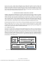
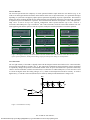
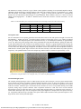
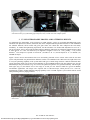
UV-LED exposure system for low-cost photolithography Murat Kaya Yapici* and Ilyas Farhat Department of Electrical and Computer Engineering, Khalifa University, Abu Dhabi, UAE 127788 ABSTRACT This paper reports the development of a low-cost, portable, light-emitting diode (LED)-based UV exposure system for photolithography. The major system components include UV-LEDs, microcontroller, digital-to-analog (D/A) converter and LED control circuitry. The UV-LED lithography system is also equipped with a digital user interface (LCD and keypad) and permits accurate electronic control on the exposure time and power. Hence the exposure dose can be varied depending on process requirements. Compared to traditional contact lithography, the UV-LED lithography system is significantly cheaper, simple to construct using off-the shelf components and does not require complex infrastructure to operate. Such reduction in system cost and complexity renders UV-LED lithography as a perfect candidate for micro lithography with large process windows typically suitable for MEMS, microfluidics applications. Keywords: UV-LED lithography, low-cost lithography, light-emitting-diode, maskless lithography, UV-LED exposure dose control, MEMS, microfluidics, microfabrication. 1. INTRODUCTION Since the early 1960s lithographic techniques have played a central role in the advancement of semiconductor process technologies which in turn has fueled the development of integrated circuits (ICs) and more recently micro/nano-electromechanical systems (M/NEMS). Today, for various applications many different types of lithographic techniques are employed including electron beam lithography,1,2 X-ray lithography,3,4 nanoimprint lithography,5,6 scanning probe lithography,7-9 stereolithography10,11 and photolithography. Among these photolithography is the most widely used technique in microfabrication. In photolithography a light source is used to generate radiation usually in the ultraviolet (UV) region. The selective passage of UV light through a photomask falling onto a photosensitive polymer (photoresist) allows transfer of the geometrical patterns on the mask to the resist layer. The light source therefore is the key enabler of photolithography and also defines the resolution limits of the technology.12 For the light source, modern lithography systems in high-volume production environments use excimer lasers like krypton fluoride (KrF-248 nm) and argon fluoride (ArF-193nm) to generate deep-ultraviolet (DUV) emission allowing patterning of features below 32 nm.13 On the other hand, academic or small volume R&D centers mostly use steppers or mask aligners with gas discharge lamps (mercury lamps) having typical UV emission peaks at 436 nm (g-line), 405 nm (h-line), 365 nm (i-line) and achieve sub-micron feature sizes.14 However, the high cost of photolithography tools and associated infrastructure requirements, limits the access to this critical technology only to state-of-the-art laboratories. As a result, widespread dissemination of lithography technology beyond microelectronics towards other engineering disciplines and fundamental sciences, and possible applications therein are inherently limited due to the cost factor. To address this problem, we have developed a low-cost, portable, light-emitting diode (LED)-based UV exposure system which makes photolithography possible even in a basic laboratory. Recently, LEDs with monochromatic emission and spectral peak in the UV range have become commercially available at low cost (~ $0.67/LED),15 rendering UV-LEDs as a possible light source for photolithography thereby offering significant reduction in tool cost and infrastructure needs. Some demonstrations of UV-LED lithography include maskless lithography with micro-pixel LED arrays,16,17 and fabrication of high aspect ratio curved structures,18,19 microchannels20 and micropatterns21 using packaged UV-LEDs. *[email protected], [email protected]; phone: 971-2-5018344; fax: 971-2-4472442 Optical Microlithography XXVII, edited by Kafai Lai, Andreas Erdmann, Proc. of SPIE Vol. 9052, 90521T © 2014 SPIE · CCC code: 0277-786X/14/$18 · doi: 10.1117/12.2046123 Proc. of SPIE Vol. 9052 90521T-1 Downloaded From: http://proceedings.spiedigitallibrary.org/ on 06/11/2014 Terms of Use: http://spiedl.org/terms In this work, we report a complete prototype lithography system equipped with a digital user interface (liquid crystal display-LCD and keypad) which provides user-defined, automatic electronic control on exposure time and power allowing accurate tuning of exposure dose within a large process window. Our prototype lithography system costs less than $250, and employs only off-the shelf components including UV-LEDs (380 nm), microcontroller, digital-to-analog (D/A) converter and electronic elements for the LED control circuitry. The functionality and patterning capability of the system is verified with a minimum achievable feature size of ~ 5 µm. 2. SYSTEM LEVEL DESIGN, OPERATION AND TEST Designing a fully functional photolithography tool requires a suitable light source and proper control of its emission. Commonly used high-pressure mercury (Hg) UV lamps are usually powered from mains supply (110/220V AC) possibly requiring transformers and AC-DC convertors depending on the exact lamp model. For instance, service manual for a common mask aligner (Karl Suss MJB3) states ignition voltages of 30kV at start-up, open circuit DC voltages reaching 180V and currents of 50A,22 which are operating conditions with potentially life threatening risks. Mercury lamps also require a cooling mechanism to operate within the specified pressure limits and to prevent lamp explosions which may result in possible harm to the instrument and to the operator by accidental mercury poisoning. Furthermore, Hg lamps require a warm-up time to operate and optics to filter out the desired wavelength from multiple emission peaks. In comparison, apart from their low-cost, UV-LEDs are inherently advantageous to operate and control compared to Hg lamps. UV-LEDs require only a few volts (3-4 V DC) to generate the needed monochromatic UV emission without resorting to additional optics. The low operating voltages and currents of LEDs create naturally safe operating conditions and alleviate the extra measures required for Hg lamp operation. These unique features allow the realization of a compact, portable exposure system with user-controlled emission behavior. 2.1 UV-LED Exposure System The prototype UV-LED exposure system has four major functional blocks (Fig.1) which are 1) the user interface, 2) control unit, 3) exposure unit, and 4) peripherals. The operator is prompted to enter the exposure settings through the user interface, and based on the user specifications the control unit automatically tunes the exposure unit to output UV light with the desired intensity and duration. Upon beginning of each new run, the system can accept new settings for exposure power and duration without requiring a restart, as well as storing the previous run’s configurations should the user decide to repeat the exposure with the same parameters. To perform such “higher-level” sequential operations, a microcontroller-based topology was selected to drive the UV-LEDs, rather than using simple switches that would place the LEDs either to “ON” or “OFF” states. User Interface Control Unit Keypad Microcontroller Display D/A converter LED driver circuitry Peripherals USB microscope Exposure Unit Fan Figure 1. Block diagram of the UV-LED exposure system. Proc. of SPIE Vol. 9052 90521T-2 Downloaded From: http://proceedings.spiedigitallibrary.org/ on 06/11/2014 Terms of Use: http://spiedl.org/terms 2.2 User Interface The UV-LED system hides the complexity of circuit operation behind a simple interactive user interface (Fig. 2). An LCD screen and keypad interfaced with the microcontroller allow users to input instructions, view operational messages depending on system state and properly adjust exposure parameters depending on process requirements. The interactive display also allows scrolling through the user-defined settings and a help-menu. When the system boots up, a password is requested to prevent accidental UV exposures. The LCD main menu has three main options: 1-New, 2-Repeat and 3Help. “New” is used to set up a new exposure configuration, where exposure duration (up to 99.9 s with 0.1 s increments) and radiant power (up to 20 mW/cm2 with 1 mW increments) would be entered and confirmed. The submenu appearing after has the options to start the exposure, modify the entered information or cancel the operation. , Enter Password Exposing... Login: 1234 nr i_at'it. Finished Exposing... 1: New 2: Repeat _:Help: j 1 Figure 2. Photographs showing some of the screens in the user interface menu. The interactive screens allow the user to setup the exposure parameters, modify entered settings, repeat previous exposure settings or cancel operation. 2.3 Control Unit The UV light intensity of the LEDs is digitally-tuned with the designed control unit which involves a microcontroller, D/A converter and LED driver circuitry (Fig. 3). The control unit communicates between different system components to sequentially manage all operations. User-defined decimal values for power and duration are represented with binary values in the microcontroller (Arduino Uno-R3 board). To control the UV-LED radiant power, a D/A converter is used to convert the digital values into analog voltages (VDAC), which in return adjust the LED driver circuitry. To achieve high accuracy, a 12-bit D/A converter (MCP4725) was selected, which provided 4096 discrete voltage levels. VCC IC + VLED VDAC + - Figure 3. UV-LED driver circuitry. Proc. of SPIE Vol. 9052 90521T-3 Downloaded From: http://proceedings.spiedigitallibrary.org/ on 06/11/2014 Terms of Use: http://spiedl.org/terms The LED driver circuitry is based on a type of linear current regulator consisting of an operational amplifier (LM741, OPAMP) to adjust the biasing of a transistor (BD139, NPN-BJT). The collector current (IC) is controlled by VDAC, which tunes the intensity of the LEDs. Through changes in VDAC, current IC flowing into the LED array is controlled and therefore the UV-LED emission characteristics are easily modulated. Table.1 tabulates various VDAC values for selected radiant powers ranging from 5 – 20 mW/cm2. With the selected 12-bit D/A converter IC could be varied with ~ 0.5 mA resolution. Table 1. List of LED radiant power values and associated current and voltage values in the LED control circuitry. Radiant power 5 mW/cm2 10 mW/cm2 15 mW/cm2 20 mW/cm2 IC 438.6 mA 540 mA 700 mA 937.2 mA VLED 2.903 V 2.966 V 3.067 V 3.197 V D/A input 0880 1100 1480 2050 D/A output (VDAC) 1.0744 V 1.3431 V 1.8071 V 2.5031 V 2.4 Exposure Unit For the construction of the exposure unit InGaN UV-LEDs (RL5-UV0315-380) with peak wavelength of 380 nm and long durability (~ 2000 h) were used.15 The needed voltage to operate is in the range of 2.4 to 3.5 V; which is considered to be low voltage. The designed exposure unit consisted of an array of 172 LEDs placed uniformly on approximately 3x3 in2 area. Due to the preset spacing of holes on the protoboard and 5 mm LED tube diameter, placing the LEDs sideby-side with minimum tilt in the vertical axis was difficult to achieve. Therefore, a zigzag arrangement was used (Fig.4a) which eliminated possible vertical tilt and resulted in higher density of LEDs providing nearly equal light illumination over the entire area. With the zigzag arrangement, the number of wires was reduced as each two adjacent columns of LEDs shared a common ground. Figure 4b and 4c show the actual assembly of the LEDs and the array under operation, respectively. The optimum distance between the sample stage and the LEDs was found to be approximately 3.5 cm. kr. ti , ,, r , , r 7, 4 . v . - C yf' r- . ,`c `fi-.: 'j" R i',- r.. -y a ' . ,.. Yiir r 4 a ~. "'fi.r.ñ.;,_ r` r i' Si, '. :, ito piJìsI=I i r{,: á r,/ r .t a r r r q- c Q ' i [. 5 f`c:1f` r i4 /.. ') Ii , ". Il Tr..l r . i ,L' r( 'r /.i ' r:1, ' r r r r. . r á Wr r'r L r 'r' '' ' r 'e. [lt{L 1, r, r s , 1 r 'v . r it . . ir.r , ,'r.r ' s{'1rS, r -. n ;Yn '3.1i [i' ,r,,ci r ` ,.A,,...'...;.-:.;,-....-: órrnrlnrrrTrnTir iin Ser Figure 4. Schematic and photographs showing (a) the zigzag arrangement of LEDs; (b) the assembled UV-LED array on protoboard covering more than 3x3 in2 rectangular area; (c) UV-LED array during operation. 2.5 Final Packaged System The complete packaged prototype of the UV-LED exposure system is shown in Figure 5. For the system enclosure black acrylic material was chosen to minimize unwanted sidewall reflections. Figure 5a shows the assembly of the system where the user-interface components were placed on the front wall for easy access and others components were secured inside the enclosure. Sufficient space was allocated for the inclusion of a fan to avoid possible heating of the LEDs especially during longer exposure durations where temperature differences could cause drift in LED emission characteristics. Figure 5b shows the picture of the system during operation where UV reflections can be observed. A manual slider and sample stage were also designed to allow proper alignment of samples under the exposure unit (Fig. 5c). An optional USB microscope is attached to the system which could be interfaced with a personal computer to view large features on the mask or patterned sample. Proc. of SPIE Vol. 9052 90521T-4 Downloaded From: http://proceedings.spiedigitallibrary.org/ on 06/11/2014 Terms of Use: http://spiedl.org/terms IOEID El El El El 1:I El 0 CI ER3 u 0 F.2 0 0 0 USB microscopEr EI - , Silicon wafer User interface Manual slider ----Ate Sample stage Reflection of LEDs (b) (c) Figure 5. Photographs of the constructed UV-LED exposure system: (a) inside of the casing showing the UV-LED assembly and control circuitry; (b) system during typical exposure; and (c) overall view of the complete system. 3. UV-LED LITHOGRAPHY PROCESS AND PATTERNING RESULTS To demonstrate the functionality of the prototype UV-LED exposure system we performed photolithography using AZ5214E i-line photoresist (Clarient, Somerville, NJ) whose compositional and spin characteristics are well established. For substrate materials, silicon wafers and pyrex glass slides were chosen due their widespread use and readily availability. To conduct micropatterning experiments, first the substrates were cleaned and dehydrated at 110°C for 3 min on a hot plate. After 5 min cool-down under ambient conditions, photoresist was uniformly applied and spin-coated at 5000 rpm for 30 s. This was followed by an immediate soft-bake at 100°C for 1 min, yielding ~ 1.25 µm film thickness.23 The sample was exposed at 100 mJ/cm2 (20 mW/cm2 for 5 s) and developed for 15 s in diluted (1:4) AZ400K developer. Figure 6 shows various microstructures that were successfully patterned on bare silicon wafers with the UV-LED system. The photomask was partitioned into different sections to accommodate both “dark-field” and “light-field” areas to verify the patterning capability of the system under both types of mask design scenarios. With the dark-field mask region, photoresist molds were created for electroplating of various MEMS structures like ring inductors (Fig. 6a) and channel-shaped arrayed electrodes (Fig. 6b). The inverse photoresist patterns were generated similarly with the lightfield region (Fig. 6c) and feature sizes in the range of 50-100 µm were achieved which are typical for MEMS, microfluidics applications. The images were acquired with a USB microscope, which proved to be a low-cost, supplementary module, lending additional imaging capability to the UV-LED exposure system which could be useful when patterning relatively large geometries. .\ t rI//I 200 pm _ f photoresist mold ' (a) : _ . I j¡bj '. _ 1100pm ! - 1 l 11111111E 1. jl .I , A EJLILI , pho oresist' : I I Silicon . .1/ L 1/././11: Figure 6. Images of patterned microstructures suitable for various MEMS and microsystem applications with relatively large feature sizes. Proc. of SPIE Vol. 9052 90521T-5 Downloaded From: http://proceedings.spiedigitallibrary.org/ on 06/11/2014 Terms of Use: http://spiedl.org/terms The UV-LED system was also tested on smaller geometries to evaluate resolution capabilities. The minimum features on the photomask were straight lines with 5µm width, which were successfully replicated onto glass substrates under the same lithography conditions described above. Figure 7 shows optical microscopic images of the patterned array of stripes having 5 µm width and pitch with uniform coverage. Although lithography on oxide surfaces is a non-trivial process due to well-known resist adhesion problems, successful results were achieved without using surface treatment methods such as HMDS (hexamethyldisilazane) priming or conducting extensive process optimizations. Further reductions in pattern size would be possible by optimizing process conditions and using higher resolution masks. (a) 10 pm (b) 10 Nm Figure 7. Optical microscope images of parallel array of 5 µm stripes obtained with Carl-Zeiss inverted microscope (a) image at 60x magnification; (b) zoom-in image of the outlined region; and (c) perspective view rendered with Carl-Zeiss Zen image post-processing software. 4. CONCLUSION A complete prototype of a tunable UV-LED based photolithography system was developed and its functionality was verified through successful patterning of features down to ~5 µm. Compared to traditional contact lithography tools, the UV-LED lithography system reported in this work is significantly cheaper (less than $250), simpler to construct with readily available components, does not require complex infrastructure to operate and offers full flexibility on exposure parameters. The system is portable, compact, offers low voltage DC operation and can be set-up in any basic laboratory. The reduced system cost and complexity renders UV-LED lithography as a perfect tool for microfabrication applications allowing patterning capability within a wide range varying from hundreds to only few microns. The prototype UV-LED exposure system overcomes the access limitations, financial and operational hurdles of conventional tools and can facilitate broader dissemination of lithography technology which is fundamental for micro and nanosciences. REFERENCES [1] Madou, M. J., [Fundamentals of Microfabrication: The Science of Miniaturization], CRC Press, Boca Raton-Florida (2011). [2] Levinson, H. J., McCord, M. A., Cerrina, F., Allen, R. D., Skinner, J. G., Neureuther, A. R., Peckerar, M. C., Perkins, F. K., Rooks, M. J., Rai-Choudhury, P. (editor), [Handbook of Microlithography, Micromachining, and Microfabrication], SPIE Press, London, 1 (1997). [3] Maldonado, J. R., “X-Ray Lithography, Where it is Now, and Where it is Going,” J. Electron. Mater., 19 (7), 699-709 (1990) [4] Pease, R. F., “Lithography and Other Patterning Techniques for Future Electronics,” Proc. of the IEEE, 96 (2), 248-270 (2008) [5] Chou, S. Y., Krauss, P. R., Renstrom, P. J., “Imprint of sub‐25 nm vias and trenches in polymers,” Appl. Phys. Lett., 67(21), 3114-3116 (1995). [6] Guo, L. J., “Nanoimprint lithography: methods and material requirements,” Adv. Mater. 19 (4), 495–513 (2007). [7] Quate, C. F., “Scanning probes as a lithography tool for nanostructures,” Surf. Sci. 386 (1-3), 259-264 (1997) [8] Yapici, M. K., Zou, J., “A Novel Scanning Probe Array with Multiple Tip Sharpness for Variable-Resolution Scanning Probe Lithography Applications,” Proc. of the 8th IEEE-NANO, 18-21 (2008). Proc. of SPIE Vol. 9052 90521T-6 Downloaded From: http://proceedings.spiedigitallibrary.org/ on 06/11/2014 Terms of Use: http://spiedl.org/terms [9] Yapici, M. K., Zou, J., “A Novel Micromachining Technique for the Batch-Fabrication of Scanning Probe Arrays with Preciselydefined Tip Contact Areas,” J. Micromech. Microeng, 18(8), 085015 (2008). [10] Melchels, F. P. W., Feijen, J., Grijpma, D. W., “A review on stereolithography and its applications in biomedical engineering,” Biomaterials, 31(24), 6121–6130 (2010) [11] Jorge, P., [Stereolithography: Materials, Processes and Applications], Springer, New York, (2011). [12] Harriot, L. R. “Limits of lithography,” Proc. IEEE, 89(3), 366–374 (2001). [13] Holmes, S. J., Mitchell, P. H., and Hakey, M. C., “Manufacturing with DUV lithography,” IBM J. Res. & Dev. 41, 7 (1997). [14] Helbert, J. N., [Handbook of VLSI Microlithography Principles Tools Technology and Applications, 2 nd edn], Noyes /William Andrew Publishing, Norwich, New York (2001). [15] http://www.superbrightleds.com/moreinfo/component-leds/5mm-uv-led-15-degree-viewing-angle-380-nm-30mw/632/ [Accessed: 26 January 2014] [16] Jeon, C. W., Gu, E. and Dawson, M. D., “Mask-free photolithographic exposure using a matrix-addressable micropixellated AlInGaN ultraviolet light-emitting diode,” Appl. Phys. Lett., 86 (22), 1105 (2005) [17] D. Elfström, B. Guilhabert, J. McKendry, S. Poland, Z. Gong, D. Massoubre, E. Richardson, B. R. Rae, G. Valentine, G. BlancoGomez, E. Gu, J. M. Cooper, R. K. Henderson, and M. D. Dawson, "Mask-less ultraviolet photolithography based on CMOSdriven micro-pixel light emitting diodes," Opt. Express, 17(26), 23522-23529 (2009). [18] Suzuki, S., Matsumoto, Y, “Lithography with UV-LED array for curved surface structure,” Microsyst Technol, 14(9-11), 12911297 (2008) [19] Kim, J.K., Paik, S.J., Herrault, F., and Allen, M.G., "UV-LED lithography for 3-D high aspect ratio microstructure patterning," 14th Solid State Sensors, Actuators, and Microsystems Workshop, 481-484 (2012). [20] Guijt, R.M., and Breadmore, M.C., “Maskless photolithography using UV LEDs,” Lab Chip, 8(8), 1402–1404 (2008). [21] Huntington, M. D., and Odom, T. W., “A portable, benchtop photolithography system based on a solid-state light source,” Small, 7(22), 3144–3147 (2011). [22] Karl-Suss MJB3 Mask Aligner Operator’s Reference Manual, P/N 080AA261 1289, Section 3.2.1. [23] Product data sheet, AZ5214E image reversal photoresist, Clariant Corporation, Somerville, NJ. Proc. of SPIE Vol. 9052 90521T-7 Downloaded From: http://proceedings.spiedigitallibrary.org/ on 06/11/2014 Terms of Use: http://spiedl.org/terms