1
Model 551
Timing Single-Channel Analyzer
Operating and Service Manual
Printed in U.S.A.
ORTEC® Part No. 733450
Manual Revision E
1202
Advanced Measurement Technology, Inc.
a/k/a/ ORTEC®, a subsidiary of AMETEK®, Inc.
WARRANTY
ORTEC* warrants that the items will be delivered free from defects in material or workmanship. ORTEC makes
no other warranties, express or implied, and specifically NO WARRANTY OF MERCHANTABILITY OR
FITNESS FOR A PARTICULAR PURPOSE.
ORTEC’s exclusive liability is limited to repairing or replacing at ORTEC’s option, items found by ORTEC to
be defective in workmanship or materials within one year from the date of delivery. ORTEC’s liability on any
claim of any kind, including negligence, loss, or damages arising out of, connected with, or from the performance
or breach thereof, or from the manufacture, sale, delivery, resale, repair, or use of any item or services covered
by this agreement or purchase order, shall in no case exceed the price allocable to the item or service furnished
or any part thereof that gives rise to the claim. In the event ORTEC fails to manufacture or deliver items called
for in this agreement or purchase order, ORTEC’s exclusive liability and buyer’s exclusive remedy shall be release
of the buyer from the obligation to pay the purchase price. In no event shall ORTEC be liable for special or
consequential damages.
Quality Control
Before being approved for shipment, each ORTEC instrument must pass a stringent set of quality control tests
designed to expose any flaws in materials or workmanship. Permanent records of these tests are maintained for
use in warranty repair and as a source of statistical information for design improvements.
Repair Service
If it becomes necessary to return this instrument for repair, it is essential that Customer Services be contacted in
advance of its return so that a Return Authorization Number can be assigned to the unit. Also, ORTEC must be
informed, either in writing, by telephone [(865) 482-4411] or by facsimile transmission [(865) 483-2133], of the
nature of the fault of the instrument being returned and of the model, serial, and revision ("Rev" on rear panel)
numbers. Failure to do so may cause unnecessary delays in getting the unit repaired. The ORTEC standard
procedure requires that instruments returned for repair pass the same quality control tests that are used for
new-production instruments. Instruments that are returned should be packed so that they will withstand normal
transit handling and must be shipped PREPAID via Air Parcel Post or United Parcel Service to the designated
ORTEC repair center. The address label and the package should include the Return Authorization Number
assigned. Instruments being returned that are damaged in transit due to inadequate packing will be repaired at the
sender's expense, and it will be the sender's responsibility to make claim with the shipper. Instruments not in
warranty should follow the same procedure and ORTEC will provide a quotation.
Damage in Transit
Shipments should be examined immediately upon receipt for evidence of external or concealed damage. The carrier
making delivery should be notified immediately of any such damage, since the carrier is normally liable for damage
in shipment. Packing materials, waybills, and other such documentation should be preserved in order to establish
claims. After such notification to the carrier, please notify ORTEC of the circumstances so that assistance can be
provided in making damage claims and in providing replacement equipment, if necessary.
Copyright © 2002, Advanced Measurement Technology, Inc. All rights reserved.
*ORTEC® is a registered trademark of Advanced Measurement Technology, Inc. All other trademarks used
herein are the property of their respective owners.
iii
CONTENTS
WARRANTY . . . . . . . . . . . . . . . . . . . . . . . . . . . . . . . . . . . . . . . . . . . . . . . . . . . . . . . . . . . . . . . . . . . . . . . ii
SAFETY INSTRUCTIONS AND SYMBOLS . . . . . . . . . . . . . . . . . . . . . . . . . . . . . . . . . . . . . . . . . . . . . . . iv
SAFETY WARNINGS AND CLEANING INSTRUCTIONS . . . . . . . . . . . . . . . . . . . . . . . . . . . . . . . . . . . . . v
1. DESCRIPTION . . . . . . . . . . . . . . . . . . . . . . . . . . . . . . . . . . . . . . . . . . . . . . . . . . . . . . . . . . . . . . . . . . .
1.1. PURPOSE . . . . . . . . . . . . . . . . . . . . . . . . . . . . . . . . . . . . . . . . . . . . . . . . . . . . . . . . . . . . . . . .
1.2. MODES OF OPERATION . . . . . . . . . . . . . . . . . . . . . . . . . . . . . . . . . . . . . . . . . . . . . . . . . . . . .
1.3. OUTPUT PULSE TIMING . . . . . . . . . . . . . . . . . . . . . . . . . . . . . . . . . . . . . . . . . . . . . . . . . . . . .
1.4. LOWER LEVEL REFERENCE . . . . . . . . . . . . . . . . . . . . . . . . . . . . . . . . . . . . . . . . . . . . . . . . .
1
1
1
2
2
2. SPECIFICATIONS . . . . . . . . . . . . . . . . . . . . . . . . . . . . . . . . . . . . . . . . . . . . . . . . . . . . . . . . . . . . . . . .
2.1. PERFORMANCE . . . . . . . . . . . . . . . . . . . . . . . . . . . . . . . . . . . . . . . . . . . . . . . . . . . . . . . . . . .
2.2. CONTROLS . . . . . . . . . . . . . . . . . . . . . . . . . . . . . . . . . . . . . . . . . . . . . . . . . . . . . . . . . . . . . . .
2.3. INPUTS . . . . . . . . . . . . . . . . . . . . . . . . . . . . . . . . . . . . . . . . . . . . . . . . . . . . . . . . . . . . . . . . . .
2.4. OUTPUTS . . . . . . . . . . . . . . . . . . . . . . . . . . . . . . . . . . . . . . . . . . . . . . . . . . . . . . . . . . . . . . . .
2.5. RELATED EQUIPMENT . . . . . . . . . . . . . . . . . . . . . . . . . . . . . . . . . . . . . . . . . . . . . . . . . . . . . .
2.6. ELECTRICAL AND MECHANICAL . . . . . . . . . . . . . . . . . . . . . . . . . . . . . . . . . . . . . . . . . . . . . .
2
2
3
3
3
4
4
3. INSTALLATION . . . . . . . . . . . . . . . . . . . . . . . . . . . . . . . . . . . . . . . . . . . . . . . . . . . . . . . . . . . . . . . . . .
3.1. CONNECTION TO POWER . . . . . . . . . . . . . . . . . . . . . . . . . . . . . . . . . . . . . . . . . . . . . . . . . . .
3.2. CONNECTION FROM LINEAR AMPLIFIER
........................................................................
3.3. OUTPUT CONNECTIONS . . . . . . . . . . . . . . . . . . . . . . . . . . . . . . . . . . . . . . . . . . . . . . . . . . . .
3.4. LOWER LEVEL REFERENCE INPUT . . . . . . . . . . . . . . . . . . . . . . . . . . . . . . . . . . . . . . . . . . .
4
4
4
4
5
4. OPERATING INSTRUCTIONS . . . . . . . . . . . . . . . . . . . . . . . . . . . . . . . . . . . . . . . . . . . . . . . . . . . . . . . 5
5. CIRCUIT DESCRIPTION . . . . . . . . . . . . . . . . . . . . . . . . . . . . . . . . . . . . . . . . . . . . . . . . . . . . . . . . . . . 7
5.1. GENERAL . . . . . . . . . . . . . . . . . . . . . . . . . . . . . . . . . . . . . . . . . . . . . . . . . . . . . . . . . . . . . . . . 7
5.2. INTEGRATED CIRCUITS . . . . . . . . . . . . . . . . . . . . . . . . . . . . . . . . . . . . . . . . . . . . . . . . . . . . . 7
5.3. LOWER LEVEL BIAS . . . . . . . . . . . . . . . . . . . . . . . . . . . . . . . . . . . . . . . . . . . . . . . . . . . . . . . . 8
5.4. UPPER LEVEL BIAS . . . . . . . . . . . . . . . . . . . . . . . . . . . . . . . . . . . . . . . . . . . . . . . . . . . . . . . . 8
5.5. INPUT CIRCUIT . . . . . . . . . . . . . . . . . . . . . . . . . . . . . . . . . . . . . . . . . . . . . . . . . . . . . . . . . . . . 8
5.6. LOWER LEVEL DISCRIMINATOR . . . . . . . . . . . . . . . . . . . . . . . . . . . . . . . . . . . . . . . . . . . . . . 8
5.7. UPPER LEVEL DISCRIMINATOR . . . . . . . . . . . . . . . . . . . . . . . . . . . . . . . . . . . . . . . . . . . . . . 9
5.8. CONSTANT FRACTION CIRCUIT . . . . . . . . . . . . . . . . . . . . . . . . . . . . . . . . . . . . . . . . . . . . . . 9
5.9. SCA GATE . . . . . . . . . . . . . . . . . . . . . . . . . . . . . . . . . . . . . . . . . . . . . . . . . . . . . . . . . . . . . . . . 9
5.10. RESET CIRCUIT . . . . . . . . . . . . . . . . . . . . . . . . . . . . . . . . . . . . . . . . . . . . . . . . . . . . . . . . . 10
5.11. DELAY CIRCUIT . . . . . . . . . . . . . . . . . . . . . . . . . . . . . . . . . . . . . . . . . . . . . . . . . . . . . . . . . 10
5.12. DC POWER . . . . . . . . . . . . . . . . . . . . . . . . . . . . . . . . . . . . . . . . . . . . . . . . . . . . . . . . . . . . . 11
6. CALIBRATION AND MAINTENANCE . . . . . . . . . . . . . . . . . . . . . . . . . . . . . . . . . . . . . . . . . . . . . . . . .
6.1. GENERAL . . . . . . . . . . . . . . . . . . . . . . . . . . . . . . . . . . . . . . . . . . . . . . . . . . . . . . . . . . . . . . .
6.2. CALIBRATION . . . . . . . . . . . . . . . . . . . . . . . . . . . . . . . . . . . . . . . . . . . . . . . . . . . . . . . . . . . .
6.3. FACTORY REPAIR . . . . . . . . . . . . . . . . . . . . . . . . . . . . . . . . . . . . . . . . . . . . . . . . . . . . . . . .
6.4. TABULATED TEST POINT VOLTAGES . . . . . . . . . . . . . . . . . . . . . . . . . . . . . . . . . . . . . . . . .
11
11
11
11
11
iv
SAFETY INSTRUCTIONS AND SYMBOLS
This manual contains up to three levels of safety instructions that must be observed in order to avoid
personal injury and/or damage to equipment or other property. These are:
DANGER
Indicates a hazard that could result in death or serious bodily harm if the safety instruction
is not observed.
WARNING
Indicates a hazard that could result in bodily harm if the safety instruction is not observed.
CAUTION
Indicates a hazard that could result in property damage if the safety instruction is not
observed.
Please read all safety instructions carefully and make sure you understand them fully before attempting to
use this product.
In addition, the following symbol may appear on the product:
ATTENTION–Refer to Manual
DANGER–High Voltage
Please read all safety instructions carefully and make sure you understand them fully before attempting to
use this product.
v
SAFETY WARNINGS AND CLEANING INSTRUCTIONS
DANGER
Opening the cover of this instrument is likely to expose dangerous voltages. Disconnect the
instrument from all voltage sources while it is being opened.
WARNING Using this instrument in a manner not specified by the manufacturer may impair the
protection provided by the instrument.
Cleaning Instructions
To clean the instrument exterior:
! Unplug the instrument from the ac power supply.
! Remove loose dust on the outside of the instrument with a lint-free cloth.
! Remove remaining dirt with a lint-free cloth dampened in a general-purpose detergent and water
solution. Do not use abrasive cleaners.
CAUTION To prevent moisture inside of the instrument during external cleaning, use only enough liquid
to dampen the cloth or applicator.
!
Allow the instrument to dry completely before reconnecting it to the power source.
vi
1
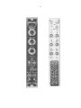
ORTEC MODEL 551
TIMING SINGLE-CHANNEL ANALYZER
1. DESCRIPTION
1.1. PURPOSE
The ORTEC 551 Timing Single-Channel Analyzer
provides a versatile group of related signal
derivation functions. It can be used as either a
single-channel analyzer or as an integral
discriminator. The principal output, furnished as
both a NIM-standard fast negative signal and a
NIM-standard slow positive signal, can be used for
accurate timing information or can be strobed by an
external input. In addition, separate NIM-standard
slow positive outputs are furnished separately for
each response by the lower level and upper level
discriminators in the module.
When the output signal is internally generated, its
timing relative to that of the input signal is derived
accurately, using a time recognition technique
called Constant Fraction Discrimination. This
technique provides unexcelled timing on either
unipolar or bipolar signals which displaces less than
3 ns for an input amplitude variation as great as
100:1. This eliminates the degradation of time
resolution for varying input amplitudes that is
characteristic of leading-edge time recognition.
The 551 accepts either unipolar or bipolar input
pulses having either RC or delay-line pulse-shaping
waveforms. It examines the amplitude of each input
pulse and generates appropriate output pulses
separately for SCA, LLD, and ULD responses. For
internal strobe operation the SCA output is delayed
from the time of recognition (at 50% of full
amplitude on the trailing edge of the input positive
waveform). The delay is adjusted on the front panel
between 100 ns and 11 s so that the output time
can be normalized to its application.
:
The instrument is designed to meet the
recommended inter-changeability standards of
USAEC Report TID-20893 (Rev). An ORTEC
4001/4002 Series Bin and Power Supply provides
all the necessary power through the rear panel
power connector. Al I signal levels and impedances
are compatible with other ORTEC NIM modules.
The 551 has a front panel switch that selects the
integral mode of operation or either of two types of
differential single-channel analysis modes. For
Normal operation, each of the discriminator levels
is adjusted independently through the full dynamic
range of 0 to 10 V. For Window operation, the
range of the lower level control is 0 to 10 V and the
range of the upper level (or window) control is the
adjusted lower level plus 0 to 1 V.
1.2. MODES OF OPERATION
Integral Mode Operation In the integral mode, the
551 generates an output through the SCA
connector on the rear panel and through both the
Pos Out and Neg Out connectors on the front panel
if the input pulse amplitude exceeds the adjusted
lower level threshold; the range is 0 to 10 V.
Normal Mode Operation In the normal mode, the
551 generates an output through the SCA
connector on the rear panel and through both the
Pos Out and Neg Out connectors on the front panel
if the input pulse amplitude exceeds the adjusted
lower level but does not exceed the adjusted upper
level threshold. In this mode, each threshold is
adjusted independently in the range of 0 to 10 V,
and the upper level must be set higher than the
lower level to permit the SCA outputs to be
generated.
Window Mode Operation In the window mode, the
551 generates an output through the SCA
connector on the rear panel and through both the
Pos Out and Neg Out connectors on the front panel
if the input pulse amplitude exceeds the adjusted
lower level threshold, but by an amount that is less
than the adjusted window width. The range of the
lower level control is 0 to 10 V, and the range of the
upper level control is 0 to 1 V above the lower level.
This mode is especially adapted to high-resolution
spectroscopy because the very narrow windows that
are required can be obtained easily and
reproducibly.
2
1.3. OUTPUT PULSE TIMING
The SCA, Pos Out, and Neg Out pulses from the
551 are generated at a delay (with internal strobe)
following the precise constant-fraction time
recognition, which occurs at 50% of the peak
amplitude on the trailing edge of the input pulse.
The delay interval is adjustable through two ranges,
selected by a front panel switch; the low range is
0.1 to 1.1 s and the high range is 1.0 to 11 s. The
front panel Delay control is a 10-turn precision
potentiometer that is marked in 1000 increments
that read the adjusted delay directly in the units.
:
:
When external strobe is used, the SCA, Pos Out,
and Neg Out pulses from the 551 are furnished
promptly at the strobe time. To be effective, the
strobe's leading edge must occur within about 5 s
(or 50 s) after the constant-fraction recognition.
The choice between the two acceptance intervals is
made with the front panel switch that is marked for
adjustable delay intervals (.1—1.1 and 1—11).
:
:
For any mode of operation, a signal is furnished
through the LL Out connector on the rear panel
when the lower level discriminator is triggered on
the leading edge of the input signal. Also a signal is
furnished through the UL Out connector on the rear
panel when the upper level discriminator is
triggered on the leading edge of the input signal.
Each of these outputs is a NIM-standard positive
signal that can be used for any desired external
application.
1.4. LOWER LEVEL REFERENCE
A rear panel 2-position locking toggle switch selects
either the front-panel Lower Level control or the
voltage signal applied through the rear panel LL Ref
connector as the reference level for the lower level
discriminator. This permits flexibility in operation,
where an external reference source can furnish the
lower level threshold from a stepped- or slidingvoltage source to automatically sweep the SCA
response through a spectral range of 0 to 10 V.
The selected source for the Lower Level Reference
is effective for all three operating modes.
2. SPECIFICATIONS
2.1. PERFORMANCE
Dynamic Range 200: 1.
Pulse-Pair Resolving Time Output pulse width
plus Delay (as selected by the front panel Delay
controls), plus 100 ns for fast NIM output or plus
200 ns for positive NIM output. Minimum resolving
time for negative output, 220 ns; for positive output,
800 ns.
Window Width Constancy <0.1% variation of fullscale window width over the linear 0- to 10-V range.
Minimum Input Threshold
Level discriminator.
Time Shift vs Pulse Height (Walk)
Dynamic
Range
Threshold Temperature Instability #0.01%/°C of
full scale, 0 to 50°C using a NIM class A power
supply (referenced to -12 V).
Discriminator Nonlinearity #±0.25% of full scale
(integral) for both discriminators.
Delay Temperature Instability #0.03%/°'C of full
scale, 0 to 50°C.
Delay Nonlinearity <±2% of delay range.
50 mV for Lower
10:1
50:1
100:1
WALK (ns)
System
System
A
B
±1.0
±2.5
±3.0
±2.0
±4.0
±8.0
System A: Using an ORTEC 460 Amplifier, single
delay-line mode, integrate #0.1 s with delay line 1
s.
:
:
System B: Using an ORTEC 471 or 472 Amplifier,
unipolar output with 0.5 s shaping time. Input from
ORTEC 419 Pulser.
:
3
2.2. CONTROLS
S
Lower Level Front panel 10-turn potentiometer
adjustable from 0 to 10 V; when the rear panel LL
Ref mode switch is set on lnt, determines the
threshold setting for the Lower Level discriminator.
When the LL Ref mode switch on the rear panel is
in the Ext position, this control is ineffective.
Window or Upper Level Front panel 10-turn
potentiometer determines the window width (0 to +1
V) in the Window mode or the Upper Level (0 to
+10 V) threshold in the Normal and Integral modes.
lnt/Nor/Win Front panel 3-position locking toggle
switch selects one of three operating modes.
Integral LL sets a single-discriminator threshold (0
to +10 V) and UL response is ignored for SCA
outputs.
Normal UL and LL are independently adjustable
levels (0 to +10 V); differential mode operation.
Window LL sets the baseline level (0 to +10 V) and
UL sets the window width (0 to +1 V); differential
mode operation.
Delay Range Front panel locking toggle switch
selects delay ranges of 0.1 to 1.1 s or 1.0 to 11 s
for internal strobe or automatic reset without SCA
output after 5 or 50 s for external strobe.
:
:
Delay Front panel 10-turn potentiometer for
continuous adjustment of output delay over
selected range. In the external strobe mode the
delay control adjusts the automatic reset time from
-5 s to 50 s.
:
Walk Adjust Front panel screwdriver adjustment
for precise setting of walk compensation.
LL Ref Mode Rear panel two-position locking
toggle switch selects either the front panel LL
potentiometer or the voltage signal applied to the
rear panel LL Ref Ext connector as the LL
discriminator reference threshold.
Strobe Rear panel 2-position locking toggle switch
selects either Internal or External source for the
SCA output signal strobe function.
2.3. INPUTS
Signal input Front panel dc-coupled BNC
connector accepts positive unipolar or bipolar
S
LL Ref Ext When the rear panel LL Ref mode
switch is on Ext, the rear panel LL Ref Ext BNC
connector accepts the Lower Level biasing (an input
of 0 to -10 V on this connector corresponds to a
range of 0 to 10 V for the Lower Level discriminator
setting). Input protected to ±24 V.
Ext Strobe In When the rear panel Ext/int Strobe
locking toggle switch is in Ext, the rear panel Ext
Strobe In BNC connector accepts a positive NIMstandard input, nominally +5 V, 500 ns wide, to
cause an output to occur from the SCA. The
external strobe should be given within 5 s (or 50
s as determined by the front panel Delay control)
of the linear input. At the end of this period, the 551
resets its internal logic without producing an output
signal if no strobe has been furnished.
:
:
:
:
:
signal, 0 to +10 V linear range, ±12 V maximum;
width, $100 ns; 100 input impedance. Rear panel
ac-coupled BNC connector accepts positive
unipolar or bipolar signal, 0 to +10 V linear range,
±100 V maximum; width, 0.2 to 10 s; 100 input
impedance.
2.4. OUTPUTS
SCA Pos Out Front panel and rear panel BNC
connectors provide positive NIM-standard output,
output
nominally +5 V; 500 ns wide; #10
impedance. For internal strobe, output occurs at the
mid-point of the linear input trailing edge plus the
output Delay as selected by the front panel controls.
For external strobe, output occurs at strobe time.
S
SCA Neg out Front panel BNC connector provides
fast NIM-standard output, nominally -16 mA (800
mV on 50 load); width, #20 ns; rise time, #5 ns.
Output occurs at the mid-point of the linear input
trailing edge plus the output Delay as selected by
the front panel controls.
S
LL Out Rear panel BNC connector provides
positive NIM- standard output, nominally +5 V, 500
ns wide; #10 output impedance. Output occurs
as leading edge of linear input crosses the LL
threshold.
S
UL Out Rear panel BNC connector provides NIMstandard output, nominally +5 V, 500 ns wide;
#10 output impedance. Output occurs as leading
edge of linear input crosses the UL threshold.
S
4
2.5. RELATED EQUIPMENT
2.6. ELECTRICAL AND MECHANICAL
The 551 is compatible with all ORTEC amplifiers
and other amplifiers having a 0- to 10-V positive,
linear output range.
Power Required
+24 V, 90 mA; + 12 V, 160 mA;
-24 V, 50 mA; -12 V, 110 mA.
Dimensions NIM-standard single-width module
(1.35 by 8.714 in.) per TID-20893 (Rev).
3. INSTALLATION
The 551 must be used in conjunction with an
ORTEC 4001/4002 Series Bin and Power Supply or
equivalent, which is intended for rack mounting.
Therefore if vacuum tube equipment or any other
source of heat is operating in the same rack, there
must be sufficient cooling air circulating to prevent
any localized heating of the transistorized and
integrated circuits used throughout the 551. The
temperature of equipment mounted in racks can
easily exceed the maximum unless precautions are
taken; the 551 should not be subjected to
temperatures in excess of 120°F (50°C).
3.1. CONNECTION TO POWER
Turn off the Bin Power Supply when inserting or
removing modules. The ORTEC NIM modules are
designed so that it is not possible to overload a
properly operating power supply with a full
complement of modules in the bin. Since, however,
this may not be true when the bin contains modules
other than those of ORTEC design, power supply
voltages should be checked after the modules have
been inserted. The 4001/4002 has test points on the
power supply control panel to monitor dc voltages.
When using the 551 outside the 4001/4002 Bin and
Power Supply, be sure that the power extension
cable that is used properly accounts for the power
supply grounding circuits that are provided
according to the recommended AEC standards
outlined in TID-20893 (Rev). Both high-quality and
power-return ground connections are provided to
ensure proper reference voltage feedback into the
power supply, and these must be preserved in
remote cable installations. Be careful also to avoid
ground loops when the module is operated outside
the bin.
3.2. CONNECTION FROM LINEAR
AMPLIFIER
Either of two inputs in the 551 can be used for the
analog signals that are furnished from a linear
amplifier. The BNC on the front panel accepts input
signals through a dc-coupled path; the rear panel
BNC accepts signals through an ac-coupled path.
The circuit through the DC Input on the front panel
is generally preferred. However, if there is any dc
baseline offset, if signal amplitudes exceed the ±12
V maximum limit of the dc circuit, or if the input
pulses decay slowly, the ac coupling that is
available through the rear panel AC Input BNC can
be used instead.
Either input circuit accepts positive unipolar pulses
or bipolar pulses (the positive lobe will be analyzed)
into an input impedance of $1000 . When long
cables (more than about 4 ft) are used to connect
the amplifier output to the 551 input, cable
termination may be necessary in order to prevent
reflections; match the cable impedance with a
terminator at the 551 input in such cases.
S
3.3. OUTPUT CONNECTIONS
The logic output pulses that are generated when
input pulses satisfy the amplitude and logic
requirements of the 551 are available through both
front and rear panel BNC connectors. NIM-standard
fast negative signals are available through the front
panel Neg Out BNC. NIM-standard slow positive
signals are available through both the front panel
Pos Out and the rear panel SCA Out connectors.
5
When the 551 is set for either differential singlechannel mode (normal or window), the logic output
pulse means that an input pulse amplitude is
sufficient to trigger the lower level discriminator
without also triggering the upper level discriminator.
When the 551 is set for its integral mode of
operation, the logic output means that an input
pulse amplitude is sufficient to trigger the lower
level discriminator; triggering of the upper level
discriminator does not affect the output.
The time when alI three SCA logic output signals
are made available is the result of either an internal
or an external strobe, selected by a rear panel
switch. When the switch selects Int, the strobe
originates from the constant-fraction trigger, at 50%
amplitude on the decay of the positive input pulse.
This strobes a delay circuit, with the delay interval
adjusted with front panel controls between 0.1 and
11 s, and the outputs occur at the end of the delay
interval. When the rear panel switch selects Ext, A
NIM-standard positive logic pulse must be furnished
through the Strobe In BNC on the rear panel and
the outputs occur at the strobe time; if a strobe is
not furnished within 5 or 50 s (selected by front
panel delay toggle at .1–1.1 or 1–11 respectively),
the internal logic is reset without generating an
output.
:
:
Separate logic outputs are available through the
rear panel to indicate when, on the leading edge of
an input pulse, each of the two discriminators is
triggered. These responses can be used to monitor
the discriminator levels during adjustment, to be
counted in external scalers, to provide subgroup
routing in a multichannel analyzer, or for any other
applications as desired. Each logic output for LL
Out and UL Out is a NIM-standard slow positive
pulse that is compatible with all ORTEC scalers,
counting rate meters, and other instruments. The
output impedance through each output path is
sufficiently low to drive as many as ten paralleled
1000 inputs.
S
3.4. LOWER LEVEL REFERENCE INPUT
if the LL Ref toggle switch on the rear panel of the
551 is set at Ext, the reference level for the lower
level discriminator must be furnished through the
adjacent LL Ref In BNC connector; the 10-turn
Lower Level control on the front panel is
disconnected. An input of 0 to -10 V through this
connector corresponds directly to a range of 0 to
+10 V for the lower level discriminator threshold.
If an input is connected to the LL Ref connector and
the switch selects Int, the signal through the
connector is ignored.
4. OPERATING INSTRUCTIONS
After the 551 has been connected into a system
according to the installation information in Section
3, the operating and strobe modes can be selected
and the discriminator thresholds can be adjusted as
required for each application.
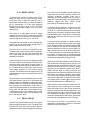
Figure 4.1 illustrates the timing relationships that
will be effective in the 551, operating with internal
strobe, for each of three possible input pulse
amplitudes. The first two pulses exceed the lower
level threshold without also exceeding the upper
level, and the third pulse exceeds both threshold
levels. Superimposed in each of these input pulses
in Fig. 4.1 is an internally-generated signal that
rises to 50% of the input peak amplitude and is
stretched at that level. When the input pulse decays
through the 50% level, the CF discriminator resets
and, when delayed by a fixed interval, triggers the
SCA outputs if the analysis criteria have been
satisfied. The delay interval can be adjusted within
the range of 0.1 to 11 s using front panel controls.
If the pulses of Fig. 4.1 were furnished to a 551 that
was set for its Normal or Window (differential)
mode, time-significant SCA output pulses would be
generated for each of the first two input pulses but
none would be generated for the third because its
amplitude was greater than the upper level
threshold. If the pulses were furnished to a 551 that
was set for its integral mode, a time-significant
output pulse pair would be generated for each of
the three input pulses. In either mode of operation,
an LLD and a ULD output will result when the
corresponding discriminator thresholds are
exceeded by the input pulse amplitude.
:
The adjusted lower level threshold is furnished
either from the front panel Lower Level control or
from an external source through the rear panel LL
6
Ref connector; the alternate selection is made with
the rear panel LL Ref toggle switch - either Int for
the front panel control or Ext for the rear panel
BNC. In either case, the range is from 0 to +10 V,
measured from chassis ground, of the input signal.
The adjusted upper level threshold is determined by
the setting of the front panel Upper Level or
Window control and by the front panel mode
selector toggle switch. When the switch is set at
either lnt or Nor, the range of the variable control is
from 0 to +10 V, measured from chassis ground.
When the toggle switch is set at Win, the range of
the variable control is 0 to +1 V, measured above
the adjusted lower level threshold.
When the rear panel toggle switch for the Strobe
source selects Ext, operation of the 551 is the same
as for Int except for the time at which an SCA
output is generated. For this mode of strobe output,
the external strobe must be furnished after the CF
trigger time and before an automatic reset, and the
SCA output signals are furnished promptly at the
strobe time. The time window, during which the
strobe can be accepted, is measured from the CF
trigger time and is either 5 or 50 s; when the front
panel delay toggle switch selects .1– 1.1, the time
window is 5 s, or when the switch selects 1–11,
the time window is 50 s. If no strobe is furnished
within the time window, the internal logic is reset
without generating an output through the SCA
circuits.
:
:
:
For optimum time-significant SCA output timing,
the front panel Walk Adj must be trimmed to the
combined effects of the input shaping and its time
constants and of the expected dynamic range of
operation. Using a duplicate of the minimum and
maximum amplitudes for shaped input pulses, set
the control to provide the minimum walk (variation
of time of occurrence vs input amplitude).
Fig. 4.1. Timing Relationships for Input and Output Pulses for Operation with
Internal Strobe.
7
5. CIRCUIT DESCRIPTION
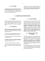
5.1. GENERAL
Figure 5.1 is a simplified block diagram of the 551
Timing SCA. It shows that each input pulse is
furnished to three internal discriminators and also
through an attenuate and peak stretch circuit. The
three discriminators are U L (upper level), LL (lower
level), and CF (constant fraction). Each
discriminator independently triggers a response
when the amplitude of its noninverted input
exceeds the amplitude of its inverted input. The
response of the UL and LL discriminators is latched
until an internal reset occurs. The CF discriminator
is reset again when the input conditions are
reversed.
Reference levels for the UL and LL discriminators
are set independently for either Integral or Normal
mode operation. For Window operation, the
threshold for the UL discriminator is based on the
LL setting instead of ground.
The CF discriminator is triggered at the onset of
each input pulse, whether its amplitude is sufficient
to trigger either of the other two discriminators or
not. Then the CF discriminator is reset when the
amplitude of the input pulse decays through its 50%
level because the attenuate and peak stretch circuit
has generated and maintained this 50% level by
that time and furnished it as the discriminator
reference level.
The SCA gate is triggered when the CF
discriminator is reset if, at that time, the LL
discriminator has been triggered and the UL
discriminator either has not been triggered (for
differential operation) or is ignored (for integral
operation). Thus the gate responds to both logical
conditions and input-pulse time significance.
If the SCA gate responds, it strobes a delay circuit
that then generates the SCA outputs at the end of
the delay interval. The simplified diagram does not
show the use of an external strobe for this output
(see Section 5.11 ).
5.2. INTEGRATED CIRCUITS
The nomenclature used to identify integrated circuit
pack ages in this manual is defined below for the
example
IC5(4)
where
IC = integrated circuit,
5 = reference designation,
(4) = pin number.
Fig. 5.1. Simplified Block Diagram of the 551 Timing SCA.
8
Any portion of an IC package can be designated by
its output pin number; in this example, the portion
of IC5 that includes pin 4 as an output is identified
uniquely.
input pulse amplitude). The gain for the level from
IC2(7) through IC 1 (1) is unity.
5.3. LOWER LEVEL BIAS
This analog input signal can be furnished through
either CN1 on the front panel or CN2 on the rear
panel. The signal is then furnished to dividers R3R4 and R47-R48, and 50% of the input amplitude is
applied to the noninverting inputs of both the UL
and LL discriminators, IC3 and IC4. The input range
of 0 to + 10 V, divided by two for an effective range
of 0 to +5 V at the discriminator inputs, is directly
equivalent to the range of threshold levels
described in Sections 5.2 and 5.3 above.
The threshold for the lower level discriminator is
adjusted with the front panel Lower Level control,
R43, or is furnished as a dc level through CN3 on
the rear panel. Switch S4 on the rear panel selects
which of these sources is effective for bias control.
For the internal bias circuit, R47 is a potentiometer
mounted on the printed circuit that adjusts the
minimum level for the front panel control. The
actual range of R43 is, then, from a few millivolts to
about -5 V. The adjusted level is buffered through
IC2(7) and inverted through operational amplifier
IC2(1), with a gain of unity, and furnished to the
inverting input of IC4, the lower level discriminator.
5.5. INPUT CIRCUIT
The input signal, through either the front panel dccoupled circuit or the rear panel ac-coupled circuit,
can be monitored at test point TP1 on the front
panel.
5.6. LOWER LEVEL DISCRIMINATOR
For the external bias circuit, a dc level between 0
and -10 V can be furnished through CN3 and
divided by R44 and R45. The result that is selected
with switch S4 is then furnished through the same
buffering and coupling network to the lower level
discriminator.
5.4. UPPER LEVEL BIAS
The threshold for the upper level discriminator is
adjusted with the front panel Window or Upper
Level control, R38. The range for this control is 0 to
-5 V. The adjusted level is buffered through ICI(7)
and furnished through either R55 or R52, through
operational amplifier IC1(1), and to the inverting
input of upper level discriminator IC3. When switch
Sl is set at either Integrate or Normal, the gain of
IC1 (1) for this adjusted bias signal is 1.0; when the
switch selects Window, the gain is reduced to 0.1
and the effective range of the Window control is
thus reduced by a factor of 10. Also, when the
switch selects Window, the level that is furnished
frorn IC2(7) for the lower level discriminator is also
furnished through R50 and IC 1 (1). Thus the
adjusted lower level becomes, effectively, the base
above which the upper level is added, and the
result is a window of 0 to I V between the lo,,ver
level and upper level thresholds (referred to the
integrated circuit package IC4 is the lower level
discriminator. As long as the input level at its pin 3
does not exceed the level at pin 4, the output at its
pin 9 is high. When the amplitude of the input
signal, at pin 3, increases above the threshold level
at pin 4, IC4 triggers and reverses the levels at its
pins 9 and 11. VVhen IC4(11) goes high, IC6(13)
goes low and latches IC4(11) in the high state until
a reset is furnished from IC7(6). The reset will be
furnished when the discriminator returns to
quiescent and the CF discriminator is also reset;
these conditions occur on the trailing edge of the
input pulse.
The signal from IC4(11) is furnished through IC8(4)
to generate an LL Out signal through CN8 on the
rear panel when the input signal rises through the
LL threshold. The output generator uses Q25, Q26,
and 027 to generate the positive output pulse with
a width of about 500 ns.
Until latch IC6(13) and IC4(11) is reset, the high
level to pin 2 of SCA gate IC7(12) arms the gate to
permit response if its pins 1 and 13 go high. See
Section 5.9, SCA Gate.
9
5.7. UPPER LEVEL DISCRIMINATOR
Integrated circuit package IC3 is the upper level
discriminator. It is identical to IC4, discussed in
Section 5.6 above, except that its output at pin 9 is
not used.
If the amplitude at pin 3 increases above the
threshold level at pin 4, IC3 triggers and switches
the output at IC3(11) to its high state. This output at
pin 11 latches through IC6(10) until a reset is
furnished from IC7(6). The reset will be furnished
when both the lower level and CF discriminators
have been reset, as discussed in Section 5.6.
At the trigger time on the leading edge of the input
signal, when IC3(11) goes high, an output through
CN4, the UL Out connector, is generated through
IC8(1), Q22, 023, and Q24. The positive output
pulse has a width of about 500 ns.
if switch S1 is set at Int, the output of gate IC7(8)
will remain high whether the upper level
discriminator is triggered or not. But if the switch
selects either Normal or Window (for differential
single-channel operation), a response in IC3 will
furnish a low signal from IC7(8) to inhibit a
response in IC7(12) and prevent an SCA output
signal from being generated.
Integrated circuit IC5 is the CF discriminator. The
inputs at its pins 3 and 4 are indicated in Fig. 4.1.
During operation, the ICS package is triggered at
the beginning of each input pulse, as soon as the
50% level at pin 4 exceeds the 25% level at pin 3
by just a few millivolts. Then, during decay of the
input pulse, the level at pin 4 drops down through
the level at pin 3 at 50% of the peak amplitude,
which is a dependable and precise time in a shaped
linear pulse, and IC5 is reset. At reset, IC5(9) goes
high to drive pin 9 of IC8 low and to switch IC6(1)
from low to high. R77 and C34 provide a slight
delay before IC6(1) reaches a high level and, during
this short interval, ICS(10) goes high. The level at
IC8(10) is one of the three inputs to SCA Gate
IC7(12).
The CF discriminator is triggered and then reset
during each input pulse, including noise pulses. The
only input pulses that will use the time-significant
CF reset are those that also trigger the LL
discriminator.
5.9. SCA GATE
Integrated circuit IC7(12) is the SCA Gate. When all
three of its inputs are high, the output switches low
and this starts generation of an output through the
SCA Out, the Pos Out, and the Neg Out
connectors.
5.8. CONSTANT FRACTION CIRCUIT
The input signal is furnished through R2 into a peak
detect circuit, formed by Q1 through 05 and C10.
During the time of the input pulse, the capacitor is
charged. The verse current path is cut off, so the
peak amplitude of the input pulse remains on C10
until it is discharged at a later time.
The peak amplitude of the input pulse is furnished
through a unity-gain buffer amplifier, Q8, Q9, and
Q10. The front panel Walk Adj control, R36,
provides a fine adjustment of the offset of this
amplifier and is adjusted for its dynamic function to
minimize walk in the time-significant output pulses.
The output of the buffer amplifier is furnished
through R33 and R31, a divide-by-4 attenuator.
From this circuit, 25% of the peak amplitude of the
signal input pulse is furnished to the inverting input
of IC5.
The signal at IC7(13) is high unless the upper level
discriminator has been triggered and switch SI is
set at either Nor or Win (the differential mode of
operation). A response by the UL discriminator, with
differential operation, will inhibit a response in
IC7(12).
The signal at IC7(2) is high from the time the LL
discriminator is triggered until an internal reset is
generated by IC7(6), and this will not occur before
the reset of the CF discriminator. Thus a response
by the LL discriminator is a prerequisite to enable
gate IC7(12).
The signal at IC7(1) is furnished from IC8(10) when
the CF discriminator is reset (see Section 5.8).
Thus, for the short duration of the signal high at
IC7(1), and if the single-channel criteria have been
met by signals at IC7(2) and IC7(13), then IC7(12)
will go low.
10
5.10. RESET CIRCUIT
An internal reset circuit is furnished from IC7(6),
going low when all three inputs are high. When
IC7(6) goes low, it resets the latch for the LL
discriminator through IC6(13); it resets the latch for
the UL discriminator (if it has been triggered)
through IC6(10); and it turns on Ql I to quickly
discharge the storage capacitor CIO in the peak
detect circuit.
At the start of an input signal, at the CF trigger
response, the input of IC7(6) at pin 3 goes low and
remains low until just after the CF discriminator is
reset [the signal from IC6(1), R77, and C34).
The signal at pin 4 goes high at the LL discriminator
trigger tirne and is latched high through IC4(11)
until internal reset has occurred.
The third input to IC7(6) is furnished from the
complementary output of IC4(9) and this goes high
when IC4 is reset. The IC4 reset occurs when the
input signal amplitude decays back through the
adjusted LL threshold.
From a timing point of view, the LL trigger and reset
must have both occurred and the CF discriminator
must have been reset before all three inputs to
IC7(6) can be high simultaneously. Either the CF or
the LL reset can occur before the other, but the
reset trigger depends on both events having
occurred. The duration of the low signal from IC7(6)
is the propagation time for the reset of latch IC6(13)
and IC4(11 ).
Since the reset circuit is dependent upon the lower
level discriminator, and since in the Normal and
Integral modes it is possible to adjust the upper
level threshold for a response at less than the lower
level threshold, this combination could result in a
single response through the UL Out without its latch
being reset until the lower level threshold is also
exceeded by an input. This condition will not exist
in the Window mode, since it is not possible to set
the UL below the LL level.
5.11. DELAY CIRCUIT
When IC7(12) goes low (Section 5.9), IC8(13) goes
high and triggers the delay circuit. The delay circuit
includes Q15, Q16, Q19, Q20, and Q21 and their
associated circuitry. When the trigger is furnished to
Q15, Q16 is cut off and held in the off state by the
signal from Q21 and C45. Q16 then returns to its
normally conducting condition when C45 is
recharged by current through either Q19 or Q17.
When Q16 is turned on again, the negative output
transition triggers the SCA outputs unless
prevented by the external strobe circuit.
For internal strobe operation, the emitter for Q19
can be set high, with S3 set at 1–11 s, or low, with
S3 set at .1–1.1 s. Potentiometer R115, the Delay
control on the front panel, combines with the Q19E
level to determine the current rate that will recharge
C45 and thus determine the recovery time for the
delay circuit.
:
:
For external strobe operation, the emitter level for
Q19 is set in the same manner, either low or high,
by S3. Resistor R114 then combines with the Q19E
level to determine the rate that will recharge C45
and thus determine the recovery time at either 5 or
50 s, and Q16 is turned on at the end of this time.
if an external strobe is furnished through CN5 prior
to recovery, the input pulse is furnished through
Q18 and Q17 to recharge C45 quickly and generate
an immediate response by turning on Q16.
:
When S2 selects internal strobe, pin 9 of IC9 is held
high. At the start of the delay interval, pin 10 of IC9
goes high and this propagates through IC9(l 1) and
IC9(6) to furnish a low to pin 3 of IC10(1), arming
this gate. At the negative transition from Q16C,
IC9(8) switches high so IC9(3) goes low and
triggers the current switch Q13 and Q14 for the Neg
Out signal; the negative transition also triggers
IC10(1) to furnish a negative pulse through IC10(4)
and start the generation of the Pos Out and SCA
Out signals. Both of these triggers are terminated
by the fast differentiation of R89 and C38.
When switch S3 selects External strobe, pin 9 of
IC9 is held low until a strobe pulse is furnished.
When the strobe occurs, gate IC9(8) initiates the
response conditions that are described above and
also triggers the recovery of Q16 through Q18 and
Q17 to initiate the outputs. If Q16 is turned on by
automatic reset without a strobe input, gate IC9(8)
prevents any output generation from occurring.
The base level for Q16 is very sensitive, so a
temperature compensating network is connected
between this point and ground.
11
5.12. DC POWER
Input power from the bin and power supply is
accepted through the module Connector on the rear
panel. The 551 operates on 90 mA through the +24
V circuit, 160 mA through the +12 V source, 50 mA
f rom -24 V, and 110 mA from -12 V.
Internally, the +12 V source is furnished to a circuit
that uses Q32 and 033 to generate a regulated +5
V level. The +5 V level is used in the integrated
circuit packages that are in the 551 circuits.
6. CALIBRATION AND MAINTENANCE
6.1. GENERAL
6.3. FACTORY REPAIR
The basic performance of the 551 Timing SCA can
be inferred from its operating responses. If the unit
fails to respond properly at any time, use the
information in Section 5 to identify the probable
fault.
This instrument can be returned to the ORTEC
factory for service and repair at a nominal cost. Our
standard procedure for repair ensures the same
quality control and checkout that are used for a new
instrument. Always contact the Customer Service
Department at ORTEC, (865) 482-4411, before
sending in an instrument for repair to obtain
shipping instructions and so that the required Return
Authorization Number can be assigned to the unit.
Write this number on the address label and on the
package to ensure prompt attention when the
shipment reaches the ORTEC factory.
6.2. CALIBRATION
There is a provision for the calibration of the CF
reference circuit. Potentiometer R17, mounted on
the printed circuit, permits this calibration. Use the
following procedure:
1. Connect a jumper between Q4C and R28. This
ties the input to the buffer amplifier at ground.
6.4. TABULATED TEST POINT
VOLTAGES
2. Set potentiometer R17 fully counterclockwise, as
viewed from the top.
The following voltages are intended to indicate the
typical dc voltages that can be measured on the
printed circuit. In some cases the circuit will perform
satisfactorily even though, due to component
tolerances, some voltages may differ slightly from
those that are tabulated in Table 6.1. Therefore,
the voltages that are listed should not be considered
absolute, but rather are intended as an aid in
troubleshooting.
3. Measure the output of the buffer amplifier at
Q9C. Adjust front panel Walk Adj (R36) as
necessary to obtain 0V ± 1 mV.
4. Remove the jumper between Q4C and R28.
5. With no input signals, adjust R17 as necessary to
obtain 0 V again at the buffer amplifier output,
Q9C.
All voltages were measured with no input signal and
with the front panel switch set for integral mode.
The level at Q20B is dependent upon the setting of
the delay range switch, S3.
12
13
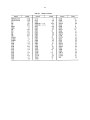
Table 1. Bin/Module Connector Pin
Assignments For Standard
Nuclear Instrument Modules per
DOE/ER-0457T.
Pin
1
2
3
4
5
6
7
8
9
10
11
12
13
14
15
*16
*17
18
19
20
21
22
Function
+3 V
!3 V
Spare bus
Reserved bus
Coaxial
Coaxial
Coaxial
200 V dc
Spare
+6 V
!6 V
Reserved bus
Spare
Spare
Reserved
+12 V
!12 V
Spare bus
Reserved bus
Spare
Spare
Reserved
Pin
23
24
25
26
27
*28
*29
30
31
32
*33
*34
35
36
37
38
39
40
*41
*42
G
Function
Reserved
Reserved
Reserved
Spare
Spare
+24 V
!24 V
Spare bus
Spare
Spare
117 V ac (hot)
Power return ground
Reset (Scaler)
Gate
Reset (Auxiliary)
Coaxial
Coaxial
Coaxial
117 V ac (neutral)
High-quality ground
Ground guide pin
Pins marked (*) are installed and wired in
ORTEC’s 4001A and 4001C Modular System
Bins.