1
TK-76glH
KENWOOD
SERVICEMANUAL
@1996.10PRINTED
INJAPAN
(tt) sgr
Bs1-8929-oo
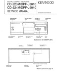
TK-768/H
Microohone
ffg1-0552-05)
Cabinet11.1pper)
(401-2112-03)
\
")
Panelassy
Frontglass
(A62-0449-13) (810-1
230-04)
TK-768/H(D)type
)
-)
Key top (Rubber)
(K29-5081-02)
Tl+7681H
CONTENTS
0
$
REALIGNMENT
2. How To Enter EachMode
INSTALLATION
1. AccessoryConnection Gable(KCT-19: Option)
2. fgnition SenseCable(KCT-18: Option)
4. Horn/Light Unit (KAP-1: Option)
6. Fitting the Control Panel Upside Down
CIRCUITDESCRIPTION
1. Circuit Configuration by Frequency
..............
I
..............
26
.........29
..................
34
e
........36
..............
37
C
DESCRIPTTON
OF COMPONENTS
.......50
s
PC BOARDVIEWS / CIRCUITDIAGRAMS
TX-RX UNIT: TX-RX (Xs7-4950-XXllAl2l
TX-RX UNIT: CONTROL(X57-4950-XXIlBl2l
........77
.....................
87
G
TK:768/H
GENERAL
I
INTRODUCTION
PERSONNEL
SAFETY
SCOPEOFTHISMANUAL
This manualis intendedfor use by experienced
familiarwith similartypesof commercial
technicians
gradecommunications
equipment.lt containsall requiredserviceinformation
for the equipmentand is
data.Changes
whichmay
currentas of the publication
are coveredby eitherService
occurafterpublication
Theseareissuedas reBulletins
or ManualRevisions.
quired.
The followingprecautions
are recommended
for
personnel
safety:
. DO NOTtransmitif someoneis withintwo feet (0.6
meter)of the antenna.
. DO NOTtransmituntilallRFconnectors
areverified
secureandanyopenconnectors
areproperly
terminated.
. S H U TO F Fa n d D O N O To p e r a t et h i s e q u i p m e n t
nearelectrical
blastingcapsor in an explosiveatmosphere.
. All equipment
shouldbe properlygroundedbefore
power-up
for safeoperation.
o Thisequipment
shouldbe serviced
by a qualified
technician
only.
REPLACEMENT
PARTS
ORDERING
partsor equipment
Whenorderingreplacement
innumbershouldbe
formation,
thefullpartidentification
Thisapplies
kits,or
included.
to allparts: components,
chassis.lf the partnumberis not known,includethe
chassisor kit numberof whichit is a part,anda suffifor proper
cientdescription
of the required
component
identification.
t
SERVICE
This radiois designedfor easyservicing.
Referto
printedcircuitboardviews,
the schematicdiagrams,
procedures
contained
within.
andalignment
NOTE
WE CANNOTguaranteeoscillatorstabilitywhen usi n g c h a n n e le l e m e n t m a n u f a c t u r e db y o t h e r t h a n
KENWOODor its authorizedaoents.
I
DESTINATION
LIST
Model and
destination
TK-768
TK-768
TK-768H
TK-768
TK-768
TK-768H
U
M
M
D
M
D
D
M2
M2
M2
Frequency
range {MHzl
148-174
TX
power(Wl
25
148-174
148-174
136-1 56
45
Microphone
Siqnalins
DTMF
tvpe (ACSY)
o
o
o
o
.)
o
Basic
16kev
16kev
Basic
16 key
16 kev
OT
136-1 56
25
25
.ó
136-1 56
45
o
DOT
-r
o
o
o
0
@
@
TK:768/H
SYSTEM
SET.UP
Merchandisereceived
RF
Frequencyrange(MHz)
148-174
148-174
136-156
136-156
?BW
TK-768
RF
Choosethetype
of trunr."i*r.
45\
Tvoe
M
DM
M2
DM2
Frequencyrange(MHz) Type
148-174
DM
136-156
DM2
TK-708H
)--!l
I
I
MIC (ACSYI
Basic
16 kev
Basic
16 key
Mrc(AcsY)
16 key
16 kev
See page 24.
programming
Transceiver
A personalcomputer(lBM PCor compatible),programminginterface(KpG-4),
(Selfprogramingor softwareprograming) and programmingsoftware(KPG-29D)
are requiredfor programming.
(Thefrequencyand signalingdata are programmedfor the transceiver.)
YES
Are you usingthe
KAP-1
I
ght unit
Horn/Li
(offi;j
|
See
Are
rrnrr
rraihd
YES
fha
NO
t
See page 34.
Installation
the TX-RXunit
when usedKAP-1.
35.
KE r-5
Externalspeaker
(Option)
_lAre you using
_YES
the i(
(Option)
I
S,:e page 29.
-',l
-c.r-18
|
I lgnitionsrrnsecable
(Option)
I
I
Delivery
0
0
::l': :'r-.';
rr::::r:.:L: :: :1.ir.',:ïi: i:3 :r 1ry:r;::rI-r.ï:j.,::ïT:ïl:=.Tï
,.I
TK.76BIH
REALIGNMENT
1.Modes
Mode
I
Function
USERMODE
Customer
usethismode.
MODE
CONVENTIONAL
This mode is for use as a transceiver.
This mode usedwhen a trunking
(SmarTrunk)
TRUNING
MODE
boardhas been installed.
DEALERMODE
This mode is used bv the dealer
for makingsettingsÍor the modes.
PANELTESTMODE
Dealerusesto checkthefundamentalcharacteristics.
P A N E LT U N I N GM O D E
Dealerusesto tune the radio.
This mode is communication
the
radioto PC (lBM compatible).
PCMODE
DATAPROGRAMMING
MODE
PCTUNINGMODE
Conventionalmode/Trunking (SmarTrunk)mode
Switch between Conventionalmode and Trunkingmode by holding
down the tMONll key in POWERON.
This can be selectedwhen installedwith a boardwith the trunking
mode function (boardmodel ST-865KW2).
MODE
DATAPROGRAMMING
PCTESTMODE
It requiresthe KPG-29D.
This mode is Írequencydata and
featureswrite to the radioand
readfrom the radio.
Thisfeatureis includethe FPU.
Thismodecancheckthe radioby
PCcontrol.Thisfeatureis include
the FPU.Thisparagraph
is as
sameas PANEL
TUNING.
Note : The SmarTrunk IIrM call is a registered trademark of the Selectone Corporation.
)
2. How To EnterEachMode
Mode
USERMODE
DEALERMODE
PANELTESTMODE
PANELTUNIN
MG
ODE
PCMODE
Operation
UsuallyPowerON then beginthis mode.
The A switch is held on with Power ON the radio. The A switch holdinqabout 2 sec. after Power ON the radio.
The D/A switch is held on with Power ON the radio. The D/A switch holdingabout 2 sec. aÍter Power ON the
radio. But,if this modeis disabledby FPUthen beginthe USERMODE.
The SCANswitch is held on with Power ON the radio. The SCANswitch holdingsabout 2 sec. after Power ON
the radio. But, if this mode is disabledby FPUthen beginthe USERMODE.
The radioPowerON to beginthe USERMODEwhen throughto the microphone
then beginthis mode.
Note : PANELTESTMODEand PANELTUNINGMODEdoesnot beointhe PC MODE.
3. Self Programing Mode
3-1. Setting the channels
The dealercan set the functions,suchas frequency
and signaling,for eachchannelof the transceiverwithout usingthe FPU.
Operation
1. Hold down the IAI key and turn the power on, and
keep the [Al key pressedfor two secondsto enter
the initialmode. The displaychangesfrom "PrOG"
to "SEL".
2. When the [MON]key is pressedagain,the channel
set mode is entered.The displayshows "CH1".
3. There are channels1 to 32. Then [D/A] key incrementsthe channelnumber,andthe [SCN]key decrementsthe channelnumber.
4. The setting items are listed in Table 1. When the
choiceis changedandthe ICHVI key is pressed,the
displayedvalue for the current item is stored in
memoryand the next item appears.
5. When the [MON] key is pressed,the initialmode
"SEL" returns.
I
REALIGNMENT
)
Setting item (Table 1)
Function name
Channelselect
Setting (Defaults are underlinedl
c H 1- C H 3 2
Display
_cH_1_
cu ea
RXÍrequency
RXOT
ïX frequency
TX OT
39_250,3_
100-550MHz
5/6.25kH2
step
450.00625
ICHAI FrequencyON/OFFselect
lAl Step select
ISCNI1 step down
[D/A] 1 step up
IVOLAI MHz steP uP
NOLV] MHz steP down
At 6.25kHzstep,dot light(Rightside).
OFF
-OFF-
67.0-250.3H2
(0.1Hz step/standard)
_ t_o / .u_
DEL
ADD
ON
_1_dEL
_1_Add_
100-550MHz
5/6.25kH2
step
450.00625
OFF
-OFF-
67.0-250.3H2
(0.1Hz step/standard)
_t_o/.u_
Blank
TX FLAGlisht.
39_250.3_
1 ScanDEL/ADD
2 DTMFsignaling
3 PTTID
ON
4 BusyCH lockout
OFF
OFF
1
_4_oFF_
_4_1_
lD/Al OFF/1/2select
_4_2_
_5_000
DTMFkey = lD inPut
2 ^trE
z
000-9999999999
ICHAIOTONiOFFselect
select
lAl 1 step/standard
[SCN]OTdown
tD/AlOTup
At 1 step, dot light(Rigntside).
TX FLAGlight.
ISCNIDEUADDselect
select
lD/AlDEL/ADD
ISCNION/OFFselect
[D/A] ON/OFFselect
ISCNION/OFFselect
ID/AION/OFFselect
ISCNIOFF/I/2select
_2_On_
_2_OFF_
-3-On-
OFF
5rD
ISCNIChanneldown
lD/Al Channelup
ON/OFF
select
ICHAIFrequency
lAl Stepselect
ISCNI1 stepdown
lD/Al1 stepup
IVOLAIMHzstepup
NOLVI MHzstepdown
At 6.25kHz
step,dot light(Right
side).
OT
ON/OFF
select
ICHAI
select
lAl 1 step/standard
OT
down
ISCNI
IDiAIOTup
At 1 step, dot light(Rigntside).
Blank
)
Remarks
5 99999
Note : Do not set the transmissionfrequencyand receivingfrequencyby difÍerentsteps. (lf the receivingfrequencyis set by steps oÍ 5kHz,set
the transmissionfrequencyby steps of SkHz,too. Similarly,if the former is set by steps oÍ 6.25kH2,set the latterby steps of 6.25kH2,too.)
I
I
10
) : ,-rc:-Ài
- , . , . - - . . , , - - --
---1=-:-J:--::-:--.^r-'$.
=---
" .:
'"
:i
'
'
'
l
'':
''
TK-769/H
REALIGNMENT
3-2. Setting the functions
The dealercan set the functionscommonto all the
channelsof the transceiver
withoutusinqthe FPU.
3. Whenthe IVOLAIkeyis pressed,
thefunctionnumb e r i n c r e m e n t sa,n d w h e n t h e [ V O L V ]k e y i s
pressed,
the functionnumberdecrements.When
the IVOLA]or [VOLV]keyis helddown,the function numberincrements
or decrements
continuouslv.
4. Change
the choiceusingthe [SCN]or [D/A]keyor
themicrophone
DTMFkey.Whenthe [CHV]keyis
pressed,
the displayed
valuefor the currentitemis
storedintomemoryandthe nextitemappears.The
settingitemsarelistedin Table2.
5. Whenthe[A]keyis pressed,
the initialmode"SEL"
returns.
Operation
1. Hold down the [Al key and turn the power on, and
keep the [Al key pressedfor two secondsto enter
the initialmode. Thedisplaychangesfrom "PrOG"
to "SEL".
2. When the [A] key is pressedagain,the functionset
mode is entered. The displayshows "150-1" or
"150-2".
Setting item (Table 2)
Function Name
No.
F version
Setting
IDeÍaultsare uncerlinedl
V H FF 1
V H FF 2
1
tMON}
Display
Function Name
No.
50_-_1
4
ID/A1
50_-_2
No Íunction
OFF
Monitor
Hornalert
J
SCAN
AUX(Scrambler)
4
DEL/ADD
SelectableOT
No function
Reverse
7
setectaDte Li I
M i n i m u mv o l u m e 0-31/1 step
Hornalert
_z_ó_
6
7
Beep
Timeout timeÍ
AUX(Scrambler)
B
DEL/ADD
Reverse
SelectableOT
_2_7_
aa
_2_9_
No function
Monitor
Talkaround
Hornalert
AUX(Scrambler)
SelectableOT
12
7
_4_8_
AO
q1t
YES
_6_0n_
NO
_6_0FF_
OFF
_7_OFF_
30-300S/30s
_7_1B0_
_3_2_
_3_3_
.7A
OR
_8-Or_B_And
Home channel
AND
cH1-CH32/1
CH
_3_7_
?a
_3_9_
_9_1_
Default
CH1
10
Dealer/tuning
Enable
1O_On_
mode
Disable
1o_oFF_
11
Clone
Enable
11_On_
Disable
11_OFF_
12
co/To
co
12_CO_
TO
12_tO_.
13
Priority
a1
DEUADD
Reverse
o
Signaling
SCAN
Home channel
4
DeÍault
1BOs
SCAN
Homechannel
-4_4_
Default12
_9_
Talkaround
^e
Homechannel
_5_
6_
_2*OFF_
2_1_
-2-2-
Monitor
ISCN]
:4-2-
AUX(Scrambler)
Reverse
3
_4_1_
Hornalert
Home channel
A l\trtr-
Monitor
z
DEUADD
Display
Talkaround
Talkaround
SCAN
IA1
Setting
íDeÍaults are uncerlinedl
No function
None
Fixed
1e
Selected
13-2_
1
TK:768/H
REALIGNMENT
Function Name
No,
14
Prioritychannel
Setting
(Defaults are uncerlinedl
cH1-cH32/1CH
Display
:unction
14-1_
29
CH1
DeÍault
i3
Look backA
0.5-5.0si0.1s
16
to
0.5-5.0s/0.5s
tó
19
20
Selected
1 7_ 1 _
29-16_
DTMFsignaling
31
lntermediatecode
n-q a-n
ót
Groupcode
O F FA
, - D ,* , #
33
Auto resettime
OFF
?
1-1 5s/1s
Selected+ T/B
17
4_
Default10s
Priority
1 7- 5 -
0.5-5.0s/0.5s
3.0s
DeÍault
18_3.0_
Dropoutdelay
0.5-5.0s/0.5s
19_3.0_
trme
3.0s
Default
Off hook scan
Enable
20-On-
Disable
20_oFF_
34
a1
22
Interdigittime
22_50_
23
Firstdigittime
!Q-200ms/10ms
50-200ms/10ms
aÁ
Firstdigitdelaytime 50-1000ms/50ms
24 50-
PTTID
Connect
25-1_
Disconnect
25-2_
Storeand send
1n
OFF
34_OFF_
transpon0
Callalert
?4
1
ïranspond(Callalert)
34-2_
Transpond(lD code)
34-335-On-
Clearto transpond YES
36
OfÍ hook decode
36-0n-
Enable
ÓFF
Disable
37
0fÍ hookhornalert
"A
a-7
Enable
An
Disable
23_50_
38
ConnectlD
000-
| ?a
################
T J-ó;_-r F F r F
It - B l a n k
nnn
t-
I
L
I se--
DTMF key = lD input, PTT+DTMFkey = Clea
26-0n-
39
DisconnectlD
000-Balnk
I sg
ooo
################
t""-""'
27_OnDTMFkey = lD input, PTT+DTMFkeY= g1s3
OFF
2A
2a
Callalert/
trn
Disable
ON
32_OFF_
NO
Both
Enable
J t_T_
code) 34-4_
Transoond
flranspond
35
50-200ms/1Oms
DTMFholdtime
*
1-7
17_6_
DiallD
30-2_
Sel call
1 7_ 2 _
Digittime
26
30_1_
CodeSO
30
Last used
21
25
29_1_
Last called
Priority+ T/B
TX dwell time
29_d_
D key assignment D code
' 1- 1 6 s / 1 s
16_0.5_
2.0s
DeÍault
Revertchannel
Display
Setting
IDefaults are uncerlined)
n Á
0.5s
DeÍault
Look back B
Function Name
No.
ON
2B-On-
OFF
,a ntrF
F nrl
Note : Set the channelsbeforsettingthe functions.
When both QT and DTMFsignalingare used,the first digitdelaytime shouldbe set to 100msor longer
to 000.
lf settingoÍ the DTMFsignalingis changed,the lD's oÍ the all channelswill be initialized
14
.
,|,.
Tt+768/H
REALIGNMENT
Íunction
3-3.Disablingthe self-programing
Youcanmakesettingsto prohibit
selfwritingbythe
userandshiftingto paneltest modeandpaneltuning
modewith the FPUor self-programing.
modeis enabled
Theself-programing
asthe default
mode
state. lf FPUis not used,disableDealer/Tuning
menu.
in the Self-programing
Cancelingshift-prohibit
Shortthe R492(0O)andshift-prohibit
will cancelat
poweron,or cancelby usingthe FPU.
TX-RXunit (B/2): Control
Foilsideview
----1
I
I
I
I
I
I
I
Y
€
sr I &."{
\\\;/
'ru*ï[ À] *\*16"
\q.\
*ffir#
&
6
\'b
etrëËs
*Ë.\lffi?
s
F/-*"*.è
e d-"
*'.1ffiË
&q'ffi
4, Panel Test Mode
When the test mode is entered,all LCD segments
light,the beepersoundsfor one second,andVERSION
SELECTmode is entered.
Use the followingkeysto selecta version:
D / A k e y. . . . . . . . . .U. .P.
SCN key
DOWN
Table3 lists the versions. The versionis selected
when the CHANNELDOWN key is pressed.
Version
V H FF 1
VHF F2
All LCD segments appear
à
&
(
cnlr-scNAUXADD
r:i r:r r-l r:i r:r r:r r:r r:i
u u Lf.Lr.Lt.u.u.Lt
Version select mode
Display
i__i
i_.i
tr'fJ i_.i! i,.ii._1
150-1
150-2
I .f i-l Lf.1...1"
i .i.i l.I l. i l"
Table 3
16
'":.:,,
;1;1.::*s,.T.-lï.1-ll---l::ij..::=!
!i,:v-.]..".,-:.-,'
,. . ".' '-r'-
',
"
-
l
'' -"*-
-l-.-'i-,".'-
TK-768/H
REALIGNMENT
4-1.TEST MODE CHANNELoperation
When the CHANNELDOWN key is pressedin the
VERSIONSELECTmode.the versionis selectedanda
channeloperationbegins.
for eachversionare listed
The channelfreouencies
in Table5, and keyfunctionsfor channeloperationsare
listedin Table4.
Key
Function
V O LU P
VOL DOWN
VOLUP
VOLDOWN
CHUP
CH DOWN
MUTEOFF
MON
A
SCN
CH DOWN
CH UP
SIGDOWN
DtA
PTT
TX
S I GU P
Table 4
tt
Channel
Signaling
table Íor usinq on tr,st mode
CH
4
6
7
8
3
5
o
7
8
10
M,DM,HDM
RX F (MHz)
TX F (MHz)
M2,DM2,HDM2
RX F (MHz)
TX F (MHz)
161.10000
148.10000
173.90000
155.10000
160.10000
165.10000
150.03000
156.03000
146.10000
136.10000
155.90000
137.10000
142.10000
147.10000
150.03000
153.03000
161.00000
148.00000
174.00000
r 55.10000
160.10000
165.10000
150.00000
156.00000
Decode
None
None
OT (67.0H2)
OT(100H2)
OT(151.4H2)
Qï l210.7{zl
OT (250.3H2)
146.00000
136.00000
156.00000
137.10000
142.1
0000
147.10000
150.00000
153.00000
Encode
None
100H2squarewave
OT (67.0H2)
Remarks
100Hzsquarewave
OT (100H2)
OT(151.4H2)
aI l210.7Hzl
OT(250.3H2)
None
None
DTMFsingletone (1633H2)
DTMF encodetone [7j
DTMF decode
Alert=Yes,Transpond=No
None
1633H2sinqletone
t7l
852Hz,12O9Hz
Code=159
Table 5
18
':i.:ra.r:3
.:I
TK-769/H
REALIGNMENT
5. PanelTuning Mode
when the tuningmodeis entered,the TUNING
MODESTARTdisplayappears
for aboutone second,
and the VERSION
SELECT
statebecomeseffective.
Thisstateis different
fromthevERSloNSELECT
state
in the TESTMODEin that the dot at the lowerrioht
lights.
sideof thedisplay
Usethefollowingkeysto selecta version:
D / Ak e y. . . . . . . . .U
..P
..
SCNkey
DOWN
TuningmodestaÉdisplay
Tuning mode versionselectstate
Theversionis selected
whenthe CH DOWNkeyis
pressedas the versionselectkey.
Whenthe versionis selectedwith the CH DOWN
key,the CH SELECT
stateof the tuningmodebecomeseffective.
il ,5,Iiii,-rititTt
DOT
The channeland signalingcan be selectedin the
same way as in the test mode.
The tuningitems are listedin Tables7 and 8, and
key operationsfor tuningare listedin Table6.
Tuning mode channel select state
il i- Í i-ifi i:i ll. ti
1t
Channel
Signaling
I i:iii,riiFrh"ft
1t
Tuning item
Key
Tuningmode channelselect
Function
VOL UP
VOL DOWN
CH UP
CH DOWN
MON
AUX
VOLup
VOLdown
Totuning
SCN
SIGdown
S I Gu p
D/A
PTT
Tuning
modetuning
Remarks
Key
To the right state
CH down
C Hu p
ÏX
Tuning data
Function
VOLUP
VOLup
VOL DOWN
VOL down
To CH SEL
Select
CHUP
CH DOWN
MON
AUX
SCN
D/A
PTT
Remarks
To the left state
Ïo the next item
Item down
Itemup
Adjustmentvaluedown
Adjustmentvalueup
TX
Table 6
20
-'#;t.'
ï.ï---
:.'""='
'=-.' -'ff--.ï-.,fïï
Tl+768/H
REALIGNMENT
Paneltuning state transition
item
T
tem No.
a
2L
2C
2H
4
Á l
4c
4H
o
OL
6C
6H
7
Tuningdescription
Remarks
Validranoe
0-255
0-255
0-255
0-255
o-255
0-255
balance
Signaling
0-255
Max deviation
0-255
Max deviation(Low)
Max deviation(Center) o-255
0-255
Max deviation(High)
0-255
OT deviation
0-255
Sensitivity
0-255
Sensitivity(Low)
0-255
Sensitivity(Center)
0-255
Sensitivity{High)
o-42
Squelch
Frequency
RF power
RF power (Low)
RF power (Center)
RFpower (High)
Three-pointadiustment
Low
Three-pointadjustment
Center
High
adjustment
Three-point
LOW
Center
High
4L MAX DEVLOW
Three-pointadjustment
Low
Center
Hish
Table 7
Datasave,next item
CH DOWNkey
Nextitem,previousitem
MON key,A key
Table 8
22
T1(í68lH
REALIGNMENT/
TH'tNÈ
6.TransceiverProgramming
6.iËËtrffiË
6-1.Introduction
usingan
is programmed
transceiver
TheTK-768/H
intera programming
machine,
IBM PCor compatible
Figdisk(KPG-29D)'
anda programming
face(KPG-4),
ure1 showsthe setupfor an IBM PC.
6-1.ffiid!
rK-768/H
+#{[EID{&ffi nu PCf^i.tHtrt
( 4H*ëil ) ,ffiË& tr È,9Ë( KPG-4
) ÍfiffiËfim
(KPc-2eD)
frfrffiffirf..fttrÊVffiÍtFáry" áHHK1
is&i.ïHflfiiÉ,Íàtrl"
port (RS-232C)
Communication
(
€'
Programmingdisk (K
Fis.1
6-2.KPG-4Description
(Optional
cable)
interface
PCprogramming
TK-768/H
to the
the
reeded
to
connect
TheKPG4is
(25D-subconnector
in
the
circuit
computer.lt hasa
pin)casethat convertsthe RS-232C
lbgicleveltoTTL
to externalsocket
level.The KPG-4plugis connected
of the TK-768/Handto the computerby a conversion
anda 25a 9-pinfemaleconnector
cable(option)with
pinmaleconnector.
6-3.ProgrammingSoftwareDescription
softwarefor the TKis the programming
KPG-29D
76BlH,suppliedon a 3.5"or 5.25"floppydisk.Thissoft3.3or later)on an
ware runsunderMS-DOS(version
machine.
IBM-PCX|,AT, or PS2,or on a compatible
and
Datacan be inputto or readfrom the TK-768/H,
e d i t e do n t h e s c r e e n . P r o g r a m m edda t ac a n b e
printed.
24
6-2.KPG-4ÊtiË,Hf
(frr+, i+HtJ\ffi&&
trÊ,rfr
)
&H D 4E!J1S
iÊÊ rK-768tlHffittFyfi|,
ffi KPG-4
frÍiE
&#* (25ft) +á'Ê,+*&Ë,ffi , EIUïERS-232
-ffiÊlrÉ)kffi^ TK-768/
€Ê,+Èx TrL Ê,+, KPG-4
Hfl.ÈFFlffiE,fi -ffiisÊi.tFtrtEfg&ffi -ffi+Ë&È
ffi, frw&#,rHÊ!-ffiË25fiÊlAlffiB, F-ffiË eil
f!ëffiE"
6-3.ffiÍE*í+i.r,Hf;
v!ffiffi#l+, u#M&È
Kpc-2eD
ËHï rK-768/H
-ffift3.5tfr'
E-ffiË
frË&, #M#ÊWffifr],ffi,
AT
PS2
t)l&.
d
fi#ftqli,'&IBM-PCD(T.
5.25
tfr.
(
3.3
Ms-Dos
ffidEfiÍÉ!
Ê
-hi8ïnflÊ!*êtJti&8,
rK-768/I{
5^trffi4
ffi*) Ttrfr. ffi.Htu#l+trJura
Htr].U&ffiHiffiH,
ffiTË
,
*
+ËHryffi
Á TK-?68/TT
i.qËÊ!ffiffiEID)+IF{J"
TK-768/H
t
D
,
D
REALIGNMENT/
TË'TNà
&4. Data ProgramMode
in
In this mode,datais writtenintothe EEPROM
the transceiver.Whenthe poweris turnedon, data
When
programmodecanbe enteredimmediately.
and commandscanbe rethe KPG-4is connected
'-PC-" is displayed
to indicatethat dataproceived,
grammodehasbeenentered.
Tuningcanbe doneusingan IBM PCandKPG-29D,
in the sameway as in paneltuningmode. Youcan
carryout paneltuningby selectingtest modeon the
menuscreenandfollowingthe instructions
KPG-29D
manual
instruction
on the screen.Seethe KPG-29D
for details.
6-5.CloneMode (Figure2)
from one transdatais transferred
Programmed
cable.
ceiverto anotherby usinga microphone
1.Turnthe slaveseton.
2. Holddownthe CHtvl key,turnthe masterset on,
and keepthe CH tVl key downfor two moresecthat
onds. "-C-"appearson the displayto indicate
clonemodehasbeenentered.
3. Connectthe mastersetto the slaveset.
4. Pressthe MONkeyon the masterset. The à mark
anddatais sentfromthe mastersetto the
appears
on the slavesetto show
slaveset. "-PC-'appears
data.
that it is receiving
the à markon the mas5. Whencloningis complete,
to "End".The
and"-C-"changes
ter set disappears
resetand entersuser
slaveset is automatically
mode.
lf cloningfails,the masterset shows"ErrOr".Repeatsteps4 and5.
lf you wish to cloneseveralsets,switcheachof
themon andrePeat4 and5.
6-4.ffiffiffifËË't
4rtrË* +, ïEffiËi.ftË Ê!ryffi5^iÉ'íà{/tÊt
EEPROM,
EÉffi&iEE, trIUiFlJË^frffiffiËË
iS&iÍEFpEU&&ffi+. E.EzrFttr
fr" E KPc-4
tB "-PC-" tÍ#,É, ffitziff^fryffiffiËËfr.
trIU&,ffirBMPC
x{iE'fÈ{nrË
+^i.tHtJrffl KPG-29
íÍiEifr, ÈËÍflm&rfiiil&fr +É!ÈËffi lEl. iÉ;SrpcEIDl
2effiH# 4+ É!ËFiflliil&mfEH,tH
Ëz\iË'EE
Jۃt
q4,Effi iEiil, i+rE^ ëiË 4w Y,ffi-zgD
Pï&ffiifi,EE
"
(K2)
6-5.€ftilËrt
Ë Ê!fr ffi
iÉË
Ê,rfrEIu )B- á iÉG'trrB ffiÍ-ËiA
& ffi
,í€ffi9Jfi -. êtElEÊ!iÉ'ÍÈm
+.
1. ÊiÉ "+ï^" É!Ê,w"
2. &4È"&t[" Ê!cHvffi, &iÉÈw, ,í*ffi&'íÈcHv
ffiWffffiUL,Ë9J'BzsFtfi4T "-c-" tÍË,
#r^Efr.^Ffit|Èfr"
3. ë& 'Ët[" f,fl "ftrl" o
-EziFtfrll,a&Íf;, +zs
4. & "&trl" É!MoN@,
'+t["
iAN, & "Í4t1" Ê!.'E
[il
ryffiÉÁ "Ëry["'-PC-"
+re, #^ "+ul" frE
^ffiJ:tr,luÊgj
*&ryffi.
'Ët["
à tÍfrïH
5. E€ftlJfifiÉ'
'- c - " fifiAÈ " Ét,flzrFt'Ê!
End"
+re, "Ífl" llj
X,
iË^HFËfr.
ÊArBHEft|JËfr'
l[REft{tr&,'&'il1" Ê!-'DzÍFiHq "Enor"
?ffi, f ÉÉE*w|ffifrws"
Ê!Éffi ' u á
fiRirtrEáffil-+trtft{*' +TÏFiÉíËfl
ttT-r"
&,*W4ffitr-W5
ËË : fiRxnÈàF4bTHF&tt,ÊZn9.fr:frFfttl
Ë&"
Note : Do not connectan usermoderadioto the other
usermooeone.
b
I
25
t
:i
TK:768/H
,i
I g#,
REALIGNMENT/
T,H'TNÊ/INSTALLATION
7. Memory Reset
of
the datain the EEPROM
Thisfunctioninitializes
the transceiver.
7-1.OPeration
1. Holddownthe [A] keyandturnthe poweron,and
keepthe tAI key pressedfor two secondsto enter
form "PrOG"
the initialmode' Thedisplaychanges
to "SEL".
2. Pressthe IVOLVIand [D/Alkeysat the sametime
to resetthe memory.ffhe displaydoesnotchange')
The modelname,F versionand tuningdatais not
initialized.
7.ïFfËËË€{È
4t'"
xfiÉíàilÉtEEPROM
E tÈ#fïEMfr#.ryJffi
:
ffi
s
7.1.RTÊfrW
1.&,ít IAJ6Ë,ïTrÈwfi* ,M&< IAJ6Ê'',íx
#!\ z tlffi, [{it^ïxlÊ'Ëtt" rPrOG:
+re, *
.'EzÍFtftfrgA
)t^UJffi+WHtt,
ES4' rSELr?ffi.
2. &4È(VOLV)fi*'& (D,/A) 6Ë, I|lXfFffi**E&
+l'"
ffi4 4'tt fr ffiUe Ë ifrffiffiT fr:frUJffi
s
INSTALLATION
1.AccessoryConnestionGable
( KCT-19: OPtionl
{
The KCT-19is an accessoryconnectioncablefor
has15
Theconnector
equipment.
external
connecting
for
selected
lines
are
signal
pinsandthe necessary
use.
1-1.Installingthe KCT-19in the transceiver
1. Removethe upperand lowerhalvesof the transceivercase'andlift the DCcordbushing(o) from
the chassis.
the pad(e).
2. Remove
0
t#
f .isÊÈrËEil'í+
( rcr-re : iË[6)
Kcr-le Ë - & E ïË&tl.*FiAá ÉtËÊÊ.rrË.ÍLÉ
ffiRá ts RÊffi4 UiËH tf ffi$JlÈÊ tÈ'.
1-1. EiE'íËtJtÊ
Ê# Kcr-1s
i. ry.TlÉ'íàflÉ0iTtrtÊ'fÁflÈiËËËffiÈW+
*,ffiq*EÊ(o) "
(o) .
C
2.HT4.H
Fig.l
(
26
TK76B/H
INSTAL1ATION
I T#,
$
B
( @).
3. lnsertthe KCT-I9cable( O) intothechassis
T h e w i r e h a r n e s sb a n d( @ ) m u s tb e i n s i d et h e
chassis.
the DCcordbushingin the chassis( G)).
4. Relocate
5. Connectthe KCT-19to the TX-RXunit (A/2)as
e (Ol.
s h o w ni n F i g u r 2
to the external
accessory
by in6. Connectthe KCT-19
sertingthe crimpterminal( G)) intothe squareplug
(G) ), botnof whicharesupplied
with the KCT-19.
3. )BKCT-19
Ê,4fi(O) ïÉ^í!J/ÈE(O)
" Ht_Ètfrfr
tftÈ,ffiEt-*,B.
(O) ÊJÈF.
4. É,trI4ËtftÉ,'ffi+tÈ&geê€Ë#tr /ÈB ( @) .
5. lrKl 2 (o) trm, )BKcr-lei€&t!Jrx-RX+Í
(N2)"
6. iEiÍ1Effiiaffi
+ffi^ÈMffiX (O) ( mááFÍrKCr(o) .
le -É€{*) t+ Kcr-leis&tljfl.ÈFpt'},í+
I
I
eFá"N
t
G)
O Squareplug
(E09-1
571-05)
àhs
crimo terminal
I
Fig.2
$
g
27
TK76B/H
INSÏALLATION/
Ë#
1-2.Terminalfunction
Name
No. {A) No.(B,C,D,E)
HK
u-z
A-1
A-2
A-3
A4
D-5
ME
U.J
IGN
D-1
DEO
A-5
D-6
B-2
B-3
MI
A-6
A-7
A-8
A-9
A-10
D-4
E
SB
PTÏ
DI
ó-l
HOR
u-ó
SO
D-7
'L",
(AP-1lnstllate(
Function
Off hook : "OPEN'
MIC hook signalinput. On hook :
M I CG N D
lgnitioninputfor KCT-18.
Detectionsignaloutput. Output impedance: 1kO or less,
Output level : 450mVrms(Standardmodulation),Outputfrequencyresponse: 0-3kHz flat
((-
ExternalMIC signalinput. InternalMIC signaloutput. (Standardmodulationat 600Q, SmV)
GND
(11.6V-15.6V),
Max. 1A
DC powersupplyafterpowerswitchon. DC 13.6V1157o
'1", PTT
"OPEN"
off :
ExternalPTTsignalinput. PTTon ;
Datamodulationsignalinput. Input impedance: 1OkQor more,
Deviation: 3kHzor more(4.5VPpinput,Max dev.4.1kHz)
Frequencyresponse: +1/-3dB (1kHz = OdB)at DC-9.6kHz
Horn alert controlsignaloutput. Signaloutput for horn relaydrive (opencollector),
e-
s
s
<_
<-
(ې<-
HR1
"L'levelduringhorndrive: max.sinkcurrent100m4
A-13
A-14
HR2
AM
MM
input.Mute: "H",Unmute: "OPEN"
MICmutesignal
e-
FSW
Foot switch (for emergency)signalinput.
SP
A.l2
tr-l
E-2
A- tc
(-
Not used.
Audiooutout. 4W at 4f,)lessthan 5% distortion.
'OPEN'
-H",
Unmute:
Audiomute signalinput. Mute :
{
t-
'L' : Emergencymode entry.
. Referto Terminalfunction on page 74, if need descriptionin detail.
. ConnectCN5 of the radioto connectorC of the KCT-1
9 insteadof to the internalspeakerconnector,if use externalspeaker
15-pinACCterminal
{
ffi+uÉE
frË (A) fr€ (B,C,D,E) &ffi
A-t
A-2
D-2
D-5
A-3
D-3
A4
D-l
HK
ME
IGN
DEO
A-5
A-6
A-7
A-8
A-9
D-6
MI
ËÊFl*tr"
D-',l
D4
PIT
A-10
B-l
HOR
A-ll
D-8
sQ
c-r
E-l
SP
AM
ffiF#È:"9PEN".
E-2
MM
ffi"H",1FffiÈ:
E-3
TXS
ffi^gáËfr"
DI
ffi157o
Prï {à€ffi^.
tFÈF
{
(-
&ru{à€ffis"ffiÊEfi : lKoE[E4\o
(tÍI&iEft'I),ffiHtr+q"l&: 0-3kHz
YlË."
ffi&Ê+ : 450mVrms
(eooo,
5mvTÊltÍlËiEfttl)
ffiH.
&il.
SB
KAP-IÉl#
(e-
Kcr-18Ê!,f;rkffi^"
B-3
A-12
A-13
A-14
A-15
2A
D-2
ËËFt#ffiffi^" Ët[:
*4J*áV
"L" , ffitÍt: "OPEN"
o
(11.6V-i5.6v)'
Ët lA"
ffi^Bfi : loKo4Ft"
fi#iAS'JË'€ffiH.
,ÍÊË: 3KHzfrEt(4.svp-p5^'ËffrË 4.1KHz.)
.
kHzFf+ 1/-3dB( lkHz:0dB)
tr+rÊJÈ: Ë DC-9.6
( f + É,&)
È,*sgEa
4 !'-EilÊfilË€ffis " 4{ry|,4
"
"1"Ê,+: ËtrytlÊ,mloomA.
4lrylUAB.J
&Ê'ËH"
Ëffiffi*. 4()Efi , 4wffi^F{' f-HA'Í 5Vo"
"oPEN"o
. fRf
. ln*&ffitl.ÈF,VrF#,WT,&HA.&Ê!
cN5Ë&3JKcI-19
&* C,L.m6EÊ*FtrZF{Ë&*"
e-
((e-
(-(-
HRI
(HR2
(((-
(
(
TK.76BIH
INSTALLATION/
Ë4Ë
$
I
( rcr-t a : iËlt6)
2.,Ë.)tËHË*ÊrË
2.lgnition SenseCable(KCT-I8: Option)
TheKCT-18
is anoptional
cablefor enabling
the ignitionfunction.The ignitionfunctionletsyou turnthe
power to the transceiveron and off with the car
ignitionkey.
lf you usethe HornAlertfunction,youcanturnthe
functionoff whiledrivingwith the ignitionkey.
2-1.Gonnectingthe KCT-I8to the transceiver
1. Installthe KCT-19
in the transceiver.(Seethe KCT19 section.)
( Q)) intopin3 of the
2. InserttheKCT-18
leadterminal
(
plug
square
with the KCT-19,
theninO ) supplied
sert the squareplug into the KCT-19connector
Kcr-18Ë- & ffiT&ffi ,f,,44rfrEffJffiWï&sfr
, É.^
tJ ÊVffi.ítÍÊV,
ffiit +,S^ ff rofI fr 4 * l{ rÉ.íàó[,
É ffi.
lnRífiffi4{Ul.gÍË4Ê8,
ltfipIl\#ffi R ^+Atufr+
ÊtFf.íÊ*tïJÍtrrÊ8.
2-I . {íKcr- 18i5&EiliË.iËtflt.
" rCr-re*Fr]
1. )KKCr-19
#^iÉ.íÈt[" ( 4E
)
2. :FKcr-18
É!+gtffiÍ (o) ïÉ^5 Kcr-le-HË
Hffinf(ffi*€ffi I (o), ffiÉt9ÈMtÉ*ïÉ^
(o) .
Kcr-leis&#$
(o).
E
)
E
\
Fig.3
KCT-18
I
b
29
Tt+768/H
INSTATLATION
I g#,
2-2.M&iHÊtI
2-2.ModifYingthe transceiver
as followsto turnthe power
Modifythe transceiver
or the HornAlertfunctionon andoff with the ignition
key.
case'
1. Removethe lowerhalfof thetransceiver
TX-RX
(0O)
the
R6
of
R5
and
jumper
resistors
2. Set
1.
(A/2)
Table
in
shown
as
unit
in'rrn*vujÉtËfl , t]& ffi,fi,*fnroïTfÍr x m
Éw44UJlg+84É9"
1.H.ËjÉ{È'trrffi
T+ÈFr}"
(08ft
rx-nx+iÉ (N2)Ê{BbrtÊffi.
2. trn*.LtfrmË*
ie) nsf,flR6"
i;
ír
Ooerationwhen KCT-I8is connected
R5
Enable
Power on/ofÍ and Horn AleÉ on/off
Horn AleÉ on/off
TableI
R6
Enable <--KCT-Í8 cannot be connected
Disable Enable
Enable Disable
Disable Disable <- Power cannot be turned on
R5and R6 setuPchart
The HornAlertfunctioncanbe turnedon andoff onlyif the functionhasbeen
to the AUXkeY.
assigned
EEtKcr-l8Ef É!*fF
R5
&+Fffi
frffifr,/*ewq\*frfr,/x
Nq\Êfr.fr,/*
R6
ËtFffi
<- 4ÉEë*KCT-18
A&TFffi frTFffi
EtFffi
AfrTFffi
r.E+FH AE+Fffi
tt
<- TÉ€ïTffIbF
R5fnR6Ê#El
Eftfa+1f q,XnttrfÊ"
fUrÊU'rlWthAIxf
.F,Ë'4dr./\gf
30
lr
-
TK-768/H
INSTALIÁTION
I T,#,
)
D
D
3. EmergencyMode
3.Fáfi#tHrt
3-1.Outline
Thetransceiver
canbe modifiedto havethe emergencymodeandinstalled
in the car. lf the driver(such
asa taxidriver)encounters
a robber,hecantransmitan
by
emergencysignalto a basestationautomatically
treadingon the foot switchinstalledon the floorof the
car.
The emergencymodecanbe activatedwhen the
power switch is turnedoff by changingthe power
switchfunctionto the LCDdisplayONiOFFswitch
function.
An externalspeakermaybe soundedor lightsmay
to warnrobbersby modifying
beflashedin emergency
KAP-I
the
Horn/Light
the option
to
driverelayoutput
installing
it
in
circuitand
the transceiver.
s-r.ffiS
trJ)ffi4 iÉ,ÍË'{/r4#
fr trá F Ê.tt A& rt f )FHq+
ïË+Ër. fiRAfl (ff{fififfi+dilt) iË-L-+ft*à
#, lfi,HawjLisffig*tiï+tr&-LÉ!ffiffi
fr+, É -
+ËÈË
ÊaÊË-+kê.{à€.
oN/oFF
E)FÉmf te4ÊEt{At[&ffi'Eas+$
fr Je
trtÊVffiVJffi
Hmf XHt, 4 D/HiÉ
FÊ.{ #ËrtÊË&itr
ffio
iÉit*EiËfl6
É!KAp-1t#flJwv\,/ ff Jtg[a# Ë,+$
Ë,ffi#wËq#sljiE{ÈóftÊr
, FJ]J&^ÈFIhF#tg
ffis
illdÍTtÉht,Às,D)g#tÈtil#
"
. Emergencymode systemchart
(Hold it down for about one second,)
)
TX 25 sec. e+ RX 5 sec.
EmergencyACK code receive
I key + Foot SW 1 push
D
[D/A]key 1 push
I
il
r1: TheemeÍgency
channelis the highestchannelin whichthe receivefrequencyis stored. The channelindicatordoes not
change,but a dot lightsto indicatethat the transceiverhasenteredthe emergencymode.
*2: The transceiver
sendsthe presetDTMFcode(SOS)Íirst,and
thentransmitsthe situationin the car,whichis pickedup with
the microphone.
Thetransmission
indicator
doesnot lightduringtransmission.
*3: lf the basestationacknowledges
the emergency,
the dot lights.
14: Holdthe foot switchagainfor aboutonesecond.
Éffi#áÊ&fi + ",íàiË#frr
E È,1-"
K áËËÊËË ÉE{àË,
êEÍA, Eê,f;Ê-+@,f;UffifriEïÈflB tr^H'áS#&fr .
*2, iníÈ lfnÊíÊÈiËfiiAÊ!DrMF(SOS)
ftíg, f FËrËÈ tÊX,
e& ffi+ ÊHn,. &ËiËËË+ËË#fr {*7FH.
*3. ru*4iliáÈ#&ej kátrd1Ë'€, El,f;
,frH.
*Á Fffi&ffiHfr*q-fj"
Fig.5
31
TK:768/H
INSTALLATION
Ig,#
3-2.iEËtrtÉ#Ë# .
. Ë#iÊHf*
iÉi$Kcr-lefr Kcr-18
t#ffiwfx
EffiTrE#Ëfl{, rLr'}Ê,iftáË^ k,€.)tt#Ëfr.
3-2.TransceivermodiÍicationprocedure
. lnstall the foot switch
andKCTlnstallthe foot switchthroughthe KCT-19
18.
Whenthe switchis treadedon,the radioentersthe
emergencymode.
{.)
. &gÍaffiff*Èffi
rx-RX-É-Í(B/2) : Ëft{ÈFr}
: *h (nqZ-r252-05,
0 &Íq)
R517
: Bln (ngz-r252-05,08ft18)
R401
Dh4i(w1) : Hln
TX-RX
+tr, (Nz) : RFSfFtr*Fr|
1.0kEftl&)
R14:*h (RK73FB2A102J,
. Changethe power switch circuit
TX-RXunit(B/2): Controlsection
R517: Remove(R92-1252-05,0O)
0O)
R401: Add (R92-1252-05,
Jumperwire (W1): Add
ïX-RXunit(A/2): RFsection
R14: Remove(RK73F82A102J,1'OkO)
Once the transceiveris modified,it cannotbe
turnedon andoff with the powerswitch.Thepower
on andoff.
anddisplay
switchturnsthe LCDbacklight
( T h ep o w e ri s s w i t c h e do n a n d o f f b y I G N I T I O N
SENSE.}
|
r
0
^ .-(1405
- EiÉIà|iIL%iEgtr,
È6Ê8ffiÉffi+xxÍTf fr
,eË. Ë,iF#XH *fT# f[ X lï y&ffift zrtr *Tfr#z\
)
{*o ( Ê,mÉ.fi,,k.í€ffi{*x+TfffrËt{.
Controlsection r
|
-
/VLCD
backlight
{
0
DTC144EK
l--t
I
a
TX-RXsection
3
KCT-19
]:gt------i
KCT-18
Fig.6
32
Outside
TK.76BIH
rNsrAHÁTt0NIË.#,
t
B
3-3. KAP-I {option) emergency Horn/Light drive
relay output modification
. Modify the circuit
Q1 : Remove(DTD114EK)
R3, R4: Remove(R92-0670-05,
0O)
R5, R6:Add (R92-0670-05,
0O)
(Remove01, R3 and R4,and add R5 and R6.)
3-3.KAP-1( iË[6 ) 5áË#mjry\/ N itgLdr#Ét*ffir
ilÊÍg
. ?ÍgÈffi
Ql: *h ( or ott+ r r )
R3,R4: *h (R92-0670-05,
0 Eftiq)
R5,R6: jÉln (R92-0670-05,
0 Eftffi)
(*h Ql,R3f,fiR4, #Hln R5Í[ R6)
. lnstall it in the transceiver
Sendthe outputwith the KcT-19and KCT-18.
. HËÊ#^iËËilr
ffiKcr-leÍ[ KCr-18
ÊiËffis{È€
D
Ol : DTDIt4EK
D 1 , 2: r S S 1 9 3
Emergencymode is operating
KCT-19 KCT-18
TK-768/H
cN4
)
12 pin
-19 KCT-18
TK-768/H
cN201
t
Ë8ffi
E
=8il^E
N,Ë
5
En E
EE
p
b
l-c6 I
KAP-I foil side view
Fig.7
33
TK:768/H
INSTATLATION
I g,#
4. Horn/LightUnit (KAP-I: OPtion)
4-1.Installingthe KAP-I in the transceiver
The HornAlert(max.2A drive)and Lightfunctions
the KAP-1W1 (3P;white/
are enabledby inserting
into CN4on the ÏX-RXunit,insertingW2
black/red)
(3P:green)intoCN201ontheÏX-RXunit,andconnect'
to CN1andCN2of the KAP-1
ingthe KCT-I9(option)
. Installationprocedure
1. Openthe uppercaseof the transceiver.
fromthe
2. Insertthetwo cables(O ) withconnectors
on the transKAP-1switchunitintothe connectors
ceiver.
the switchunitboardon the chassiswith
Secure
3.
two screws(O ) with the notch(O ) in the board
placedat the frontleftside.
A.WE!\,/*TjE
+7tr ( xnP-t:it[6 )
4-1.{+KAP-1#^iBËut
Wl (3P;aE,/RE/nE)
iÉi${+KAP-I
ffi^
TX/RX
+Í-Lfr cN201,+ÍtsKcr-le(iËfil) Ë&9JKAP-lff!
( Ët za WAr)ffiN
cNl fil cN2, ffiÊE'íÊí+4r|rylgÍE
ftÍrtÊafr.^ÍfF{t#"
. Ê#Ë#
L+ÈF ïxlLffi
1. ff#rÉËtnffJ
"
(o) ïÉ^s|JiÉ',íË
2. ïEmffi*ÊK.tp-r
trËÊ+*Ê!Éffi
trPíiE&#*+"
)ffi.t
3. ffim&f,Ra(@) Ítsfirês-ÍffiffiÈ-É{i|l!4.L,
É!ffin(O) 4ËïËffiUt|.
t[-2.ModiÍyingthe transceiver
. Horn Alert
(CPU)
on theTX-RX
Thesignalfrompin62 of 1C409
KAP-1HA
drives
unitturns013 andQ14on andoff and
of
relayK2to drivethe hornwith a maximum 24.
Thedefaultoutputis HR1.Therelayopenoutput
canbe obtainedbetweenHR1andHR2by removing
R1in the KAP-1.
R1
HR1(DeÍault)
Enable
r--'
Output form
-L
Disable
HR2
il,,
0
4-23Í#iÉ.íËfrr
. m|IFltgË
(cpu) w+tffi624.Ë*-fr1F"
Á Tx-RxFÍt rc40e
€:t4Q13ffl Q14+Ifffl*|fl#gEA KAP-IHA{€iËK2
UÈAffiiF.h2AtrÍ4tlUl.
ft'È'ffisÈ HRl. iÉil*h KAP-Ifï R1ÊEryí+
HR1
f[ rR2ZIE]trl1BÊ{*frffiffiÉ"
ffiilM't
RI
HRl(fi€)
ftTFH
tr
t<HRl
l
-
AfutEffi
HR2
il:,,
0
lI
I
r+l
.....-
n
I
[n I
o
Fig.9
Fig.8
(
KAP-I foil side view
(
TK-768/H
INSTALTATION
I T#.
'
D
4-3.Others
lf the HR2arenotnecessary
andthespeaker
output
is outputto an externalunitthroughthe KCT-19,
connectthe KCT-19
C connector
to CN5on theïX-RXunit.
4-3.H.ÍË
lrRï.ffis HRz*LthF*$ffiSËrEiJ Kcr-lefff
rx-RXtÊí cN5
fi3|Jfl.Èp+Í,{+Kcr-lecÊJkisr*g|J
T/VO
TX.RX UNIT
D 1 , 2: 1 S S 1 9 3
\
HR1
E
>Ë
il
(
i Emeroencv
' mOOe
)
erminal
6 : Earth
1 0 :H R I
' 1 2 ;L I O( H R 2 )
)
5. fl'ËtJftËË*
5. External Speaker
5-1.KES-3
: Option
5 - 1 .K E S - 3 :Ë M
TheKES-3is an external
speaker
for the 3.Smm-dia m e t e rs p e a k ejra c k .
. Connectionprocedure
1. Connect
the KES-3
to the3.Smm-diameter
soeaker
jackon the rearof the transceiver.
- + ffiT 3.5mm
KES-3Ë
tF#FtA
H:tíïhF+XffitLW
f
ÁÈo
. isf*fm
1. :l+KES-3
l.5mm
iS&4|JiÉ'íÈt/tËE
H:4Akf+hF#+n
7l
JUO
t
il
Fig.11
35
TK-768/H
INSTALLATION
I g,#.
6. Fitting the Control PanelUpsideDown
The ïK-768/Hcontrolpanelcan be fitted upside
canbe mountedwith its interdown,so thetransceiver
(inthe upperhalfoÍ the case)facing
down
nalspeaker
in yourcar.
the upperandlowercaseof thetransceiver
1. Remove
the mainunit(O)'
andremovethe panelfrom
(O
thedirection
change
anO
cable
flat
the
)
2. Remove
((s).
flat
cable
the
of bending
3. Turnthe panelover( @), insertthe flat cableinto
the mainunit(@). Attachthe panelto the main
the cases.
unit,andreinstall
6.HftllEiffiFJË#gd,
TK-768/rlËfttlffi
&q UIESITiSíï*EB' EIIILEI
(
uwfrÈFljhF{* {ÈrÊ+Êtt +*Fr} ) ffitrTË#FlJ
q
m
,í6Ê!ït+^.
#ÁÈtr (o) IBTF
1.ry.TiÉ{ËurmrÊruTÊ,
&o
2.F.TH+Hffi(o) , +&ÈH+È,4ËÊtëffiÈrtu
(o).
(O) f^
(@) , :l+H+ÊrlËH^Èó[
3.{+Étffi*ra
"
Ê wwffi.xwrtjÈ{tl# É tr#^ Ê Í "
{
6
{
36
TIG76B/H
GIRcU
ITDEscRI
FAffii,fi,HI
PTION/
D
e
)
1.HWfr+A
1.Gircuit GonÍigurationby Frequency
The receiveris a doubleconversion
superhetwith a
first intermediate
frequency(lF)of 45.050MH2
anda
secondlF of 455kHz.Incoming
signalsfromthe antennaare mixedwith the localsignalfromthe PLLto
producethe firstlF of 45.050MH2.
Thisis thenmixedwiththe44.595MH2
secondlocal
oscillator
outputto producethe 455kHzsecondlF.
Thisis detectedto givethe demodulated
signal.
The transmitsignalfrequencyis generatedby the
PLLVCO,andmodulated
bythe signalfromthe micro.
phone.lt is thenamplified
by TXamplifier
andPAamplifier,andsentto the antenna.
&&ÈF*tr:tLÈffiffit1.ÊÈrt, ff - +ffi ( IF)
Ë45.05MH2
, ffi=+ffih 455KHzo
A,X&&WffJÊE
5* É trÍHrfiE ffi ( PLL) Ê0ffi-+ffi ràEtAffiÈH
45.050MH2
Wffi- +ffi ( IF) Ë€, fÀEttË€Ír
44.sgsMltz
Ê!H :4ffi .ÍàEtnffiPÈ.455KIIZ
Wffi:+ ffi
'ÍË€, H :+ ffi{r-;
+4f,H,ffiPÈffilflÈ E "
Ëff ,fÈ€É trtH4 Èffi+ Ê!EËffi #{*H &r +.,
e* Ê iÉffiÊtÈffi Ë€iEftiltrtr^ ÊFfg[afr Jt{*ft
t, ïIJIEÊtÊ€FÉxrnr:+fr Jtásfr
tíJ ffiÈtr+
ÊtXtrXtÈ"
148-174MHz:M,DM;HDM
1 3 6 - 1 5 6 M H :zM 2 , D M 2 , H D M 2
45.050MH2
44.595MH2
193.05-219.05MH2
: M,DM,HDM
181.05-201.05MH2
: M2,DM2,HDM2
)
Fig. 1 Frequencyconfiguration
)
2. ReceivingSystem
2-1.RFunit
An incomingRFsignalfrom the antennaterminal
passesthroughthe antennaswitch(D20,andD24 are
off)andthe bandpass
filter(L208).Thesignalis amplified by RFamplifier0208, and passesthroughthe
bandpass
filter (L205,206,2071again.
The resulting
signalgoes
to the firstmixer(0,2071,
whereit is mixed
with the firstlocaloscillator
signaloutputfromthefrequencysynthesizer
to producethefirstlF 45.050MH2.
2.Ë&Ê[
2-1.sfffi+fr
,r.rrÊffi+ffi LfrïÊtffiÈEiÉiÍr(4 #&lÍ Je( D
20ffiD
24ffijt,)f[ffiiÉtË&{*(L208)tr , fr.L^tffiffi
(
t # * Q 2 0 8 )t r t " f , É + í i É i Í t r j É I f & *($L
205,206,207
), rái$lRi&É!Ë€Ë ^ffi *lg,ffig# ( Q
2w) , 5*Êffi+êfrFÍÉ!tr-4ffiË€18ffi, rH
{È€"
ffi-+ffi (45.050MI{z)
il
)
37
TK.76B|H
PTION/Êffii,I,HË
ITDESCRI
GIRGU
G
2-2.lF unit
Thefirst lF signalthen passesthrougha four-pole
by
crystalfilter(XF1).Thesignalis amplified
monolithic
goes
lF
unit.
and
to
the
second
O16
first lF amplifier
ThesecondlF unitconsistsof an lF systemlC (lC7)
second
andthe secondmixer,secondlocaloscillator,
lFfilter,andFM detector.lC7mixesthesignalinputto
outputof
secondlocaloscillator
it with the44.595MH2
(X2)to producethe secondlF of
the crystaloscillator
455kHz.
The455kHzsignalthengoesthrough455kHzceby the limitingamplifier,
ramicfilterCF201isamplified
FM detector(inthe
by the quadrature
demodulated
samelC),andoutputto the receiveaudioamplifier.
2-2.+ffi+78
()G1),
ffi-+ffiÈ+iÉi$-+ 4tesffi,í+ffitÉ{*
lffilÊtrÊ!'íÈ€hffi-+ffiffi1{Ë (Qt6) ilt, f*trriËÀ
ffi=+ffi+n"
ffi=+ W+ttffi&lL,ft + ffi^^,Rfr Bffi ( I c
7) , @ffiÊH-tflffi#, H:+ffi, H:+tnlRW{#fE
sffi{* (ffiiE) , &Tc7+, ffii^Éoffi-+ffi,Íà€5ffi
lfrffiffi# (x2) ffiHÊí44.5e5MHz
ÊlH:AffiíË€fE
-+ ffil;àE
tuïffi
m, f +.455KH2
"
45sKHz
ffiffi=+ ffiÈ€iÉ1Í45sKHz
Ê!@ffi,8W**
(cF201)ffii&E, &pE0Eilt#ÈÍt, f trË^êÊ
+f'+&W#Êtsffi*F ití1ffi1fl( frlFJ-+*frÊfiS
SíË'€iËít&'ltÈffiÈIt*F.
F ), ffiiEtrÊ!ffi
2-3.Audio amplifierunit
by lC2(212t',
The demodulated
signalis amplified
filterconsisting
of 1C403
andgoesthrougha low-pass
(212l,,
(1121,
anda
filter consistingof 1C403
a high-pass
(l2l to removethe unwanted
BEFconsisting
of 1C405
audiosignal.
cirThesignalthepassesthroughthe de-emphasis
of the AF switch(0406on)and1C405
cuit consisting
(2/21,andthe volumelevelis adjustedby the ICOD/A
converter.Theresulting
signalgoes
to audioamplifier
lC11, is amplified,
andis outputto the speaker.
2-3.Ëffiffi*+7E
ïftwF Fí,íË'€Èrcz (2t2)ilt{*fiJt, FÉ u
rc403( u2)hvJ},ffJ.íftiÉtÊwd*,
urc403Qn\ bPZ''x,
É0
Ë jÉffi& a#t))&t))rc405( rD h &'L,ffJFÊ
w ffiw #$ltÉ
tÊ, ffihrLffwÈffir-"+"
rái$ffirÉffi,ÍË€iË^É
Èffi (AF)lt)ê (Q 406+
iÉ) fr rc40sQD tàfi Fr*mÉ ËE6itíl*mÉft '9,
iáiÍ414Ê!Èffi,Íà€iÉi$È rc6D/A( W+,/ Ë.tN)\
È&
á${6frÊoÈËffir€$ff it^Èffifr táF ( rcl I ) ÈÍt,
ffttrÊ!ffiH tra?tË)tthË#"
2-4.Squelchcircuit
and
The detectoroutputis amplifiedby lC2 (2121
(2/
passesthrougha high-pass
filterconsisting
of 1C401
2),whichfiltersthe noisecomponents
fromthe signal.
0420 convertsthe noisepulselevelby hysteresis
and
appliesit to the CPU(1C409).
TheCPUcountsthe pulses,integrates
them,and
turnsthesquelch
on andoff according
to thecalculated
value.
2-4.ffiErgffi
&WEÊ!ffiH
È+4.rC2(2t 2) Wir#ffi.t, +iiÉ
a2) tqffiffiHiÉlÊw+Ë,
iÍ-+É rc401(
Á,íà€+€E
fi 4ËÈFr|, IBÈFàBË'íàëÉ
È&ÈBËftïl4€
Q420
cpu(rc40e)(ffi4b4{*) .
+, gÊwÊFLËjËít
cPUxfËÏWi.tW* ttT;B,iïËH, CPU
ffiffii.tHË
trfr (4*tïJ ) #4.
D20,24
L208
BPF
0208
RFAMP
1205-207
BPF
Q207
1st MIX
xF1
MCF
016
1stlF
(
a
tc7
MIX,DET,IF
lst LOCALOSC (PLL)
rc2w21 1C403|.U2',,
tc103l2l2l tc405(1/2)
AF AMP
LPF
HPF
BEF
0406
tc405Ql2l
lc11
AF PA
(
VOL
FlS.2 Receiving system
(
38
,.,
'" -:, 't,: j,,,..,,.i:*j.ïïí,,ïiriïiïr,.r
-,.
. , : l ; : . , , i _: . : , , : : : , , ' . . < . 1 . ' . . ; 1 ,.1; , : ' ' . ' . . ' :' : ' : : - ; . . - . : ; 1 . . ; , ; ; . = ; i . j , . : : 1 r . . ; r : ; r _ L r ; . - ;
Ttc768/H
)
a
)
CIRCU
ITDESCRI
PTIO
N/FEffiË HN
3.ËSJËF
3.TransmitterSystem
3-1.Microphoneamplifier
Thesignalfromthe microphone
goesto the micro
phonemuteSwitch(Q403off), lt thenpassesthrough
the high-pass
filter in 1C402(212l.
andthe pre-empha(1121.
sis/lDCcircuitin 1C402
Thesignalis applied
to the 1C404
summingamplifier
and mixedwith OT from the CPU(1C409).lt then
passesthroughthe splatterfilter(thefourthlow-pass
(112,212]',
filter)consisting
of 1C406
whichremoves
unwantedharmonics.
Theoutputfromthe low-passfilteris inputto the D/
(lC6)toadjustthe modulation.
A converter
3-1.iËÊfft*+E
ÁiÉÉrffi
^ ÊtÈ ffitr'"
Et$tiÉ ffiffiÈ#x (Q403&
Jt') tr^É rc402
Qn) &frÊ!ËjÉtË&**,iáiÍtË&
ffif="
E& rc402( U2)fr:frffilnÉ,/wffiffi.t ( rDcÊ,
ffi) 4I4.
,ái$414Ê!{È€&jË^ rc404
Ê!il Ëtrn{*ft * Ê
cpulÍ crcssuÈfrË€lEê , f E jEi$fr rc4061n,2l
( ffi4{ftiÉ}B**
2) t6frÊ!{ÍiËffiw{#
) uffihfttrÉ0*
ffi{Ë€.
iEi$Í{ftiÉffiw#É0{àëË^D/A4&# ( rc6) D{
iEHiEfi{Ë.
From
Microphone
D/A Converter
tc6
Fig.3 MicrophoneampliÍication
)
)
3-2.Finalamplifier
Thesignalfromthe PLLis amplified
by driveamplifier (0205,206)andpowermodule(1C501)
to an output levelof 25W45W,andgoesthroughthe antenna
switchD20andharmonic
filter,andon to the antenna
terminal.
lC13filzl compares
the DCinputto pin2 with the
reference
voltageat pin3 appliedby ICB(1/2),ampli(Q22and
fiesthe result,andcontrolsthe DCamplifier
O23)to keepthe transmitfinalcurrentconstant,
thus
keeping
the transmitoutputconstant.
3-3.APCcircuit
The directcurrentthat flows throughthe power
produces
module(1C501)
a voltageacrossresistors
R108.Thisvoltageis applied
to pin6 of lC13l2l2l,and
is inputasthe reference
voltagedifference
of pin5 and
amplified.
3-2.tfrË*ËË
* É t r f H 4 ( P L L ) É t Ë € É H f f iÈ t J t á #
( Q205,Q206
) ffit, f*F+i fr.^X&Írt+fr Jt+Ffrt U
D20fr iHWlg&{F,Ëftiá*ffitr
"
rc13( u2) ffiffi2 HÊ!Éffiffi^ÊEfiÉ
rc8(1/
2) E L+g|ffi3 WffJ4t HE+Ebh&, tL#.Ê<J**
*Wffi.
x, Mffiwfif{à€, Ëft||ËffitrJt# (Q22frrq.,;3)
, t))
4*WÈ.WXetrt # É!Êifi Êg
E Ë.
3-3.Ê drdr*Hf;tlËffi ( A P c )
ffi,firrt4lffiWÊlHffi
Èffiê Rl08Ê,ffi.
mffiÈ4 - f
(2n)
rc13
ÉE, ÉLË,EfigJ
WH6m, +f[ 5ffJ4t
)
)
Fig.4 Transmitpower circuit and APGcircuit
39
TK_768/H
DESGRIPTION/
CIRGUIT
Éffiiff, HN
4.ffi+ÊFlËF+zc,
4. FrequencySynthesizerUnit
4-1.VCO/PLL
the transmitsignalandthe first
The PLLgenerates
receivesignal.TheRFsignalgenerated
localoscillator
by 05 (TX)or 02 (RX)in the VCOunitis amplifiedby
unit.
signalis outputto theTX-RX
03, andthe resulting
TX and RX 05 and 02 are switchedby turningthe
sourcelinefor Q5 and02 on andoff. Thisis doneby
by
04 and01 usingthe controlsignal(STR)generated
converterin the TX-RXunit. The
the serial-to-parallel
RFsignalpassesthrough03 of the VCOunitandamplifier0209 of the TX-RXunit,and is inputto 1C202
(PLLlC).The12.8MHzPLLreference
signalgenerated
(X1)
TX-RX
unit
is alsoinputto
in
the
VCXO
the
by
tc202.
to the division
Bothsignalsare dividedaccording
produce
12.5kïzsignal.
a
unit
to
control
from
the
data
phase
sigphases
a
difference
and
are
compared,
The
(in
pump
passes
the
charge
through
and
is
nal output
produce
lug
lead
to
filter
of
the
low-pass
the
lc202land
the controlvoltagefor A5lQ2(VCO).Thisvoltageis
to D3andD4 (l'X)or D1andD2(RX)intheVCO
applied
keep
the VCOfrequencyconstant.Theother
unitto
(O1B),
by the RFampliÍier
outputfrom03 is amplified
RF
via
the
receive
unit
transmit
or
andoutputto the
(D17).
switch
( v c o )/fi1ffis ( PLL)
4-1.Is;Effi!ÊËË
(
PLL)
F +.È.ffilrà+fi&'|!H Ê!H-flÉ
É tritH4
.íÈë, ÈEïàffiffi# (vco) +ÍÊt Q5(Êff ) 4 Q2
(&'lÍ ) Peffiffffi,íÈ€&Q3ilt, &trtÊ!'ÍË€ffi^
{
(Q5)fi&& (Q2). &rx-nx
f!+iEfrxmweÈ.fit
A&{*f +.- +ïàftt|íÈ'€
FÍ+ Y1#11-*'fr
( srR) , iÉjdQ4ÍtrQrËft||Êff( Q5) ffl&rl! ( Q2)
vco +/EÉtQ3fil rx-RxtsÍ
Ê!Ê&" f'Jm'ÍÈ'€iÉi$
ilt+*ili\E)t^1C202 (PLLIc)" É TX-RX
ÊtQ209
Ê!
+Í+P! vcxo (EÊffi{tffiík#> PHffJ12.8MHz
trfErli (PLL)ewffiÈÊ+tffi^llj rc202.
il frrlfrT-'
m,| ffi^ Ê € & ffiràfttJF,ính ft.wft fifrbY
Ê!'ÍÈ€, f*tr m+'ÍÈ€it6fH {n
,|ffi , frÈ.h lz.sY'tiz
F (ê
tL+L ffiSfEffiÊ.ÈE,itH'ÍÈË{Ë€iÉi$Èíf
rc202+
È4,-+#ftl| vco
) EFiÉiÍêË1,íftiÉffi1É{#,
(Q5/Q2)
vco +-ÍFtr!
fïÉE{È€, r}tÊ,E'ÍË'€rJrS!J
vco
D3Í[ D4(Eht> 4 Dl f[ D2(ï*'&) -t, u,íRl+
ffiFWf,áË. Q3 Ê!fr - r#ffiS,ÍË€É ftffi ,It *Ë
(Qr8)
teÍl
tl Po
{
018
Dl7
r-:
l*rx
l*nx
tc202 PLLtc
PLL DATA
cK (clocKl
DT (DATA}
EP (ENABLE)
Flg.5 PLLunit block diagram
40
{
-
,^;ji-ri;;,Á1Étr-.!sj;+",.-":'*
-,:.,--;.,.::r.::i,;-;..:.
"..,:..
:':.:,:;.-.-.;r;.:;:
.;.;.:j.:,
,-,.-:: -::. , ;.'. ,o,;
TK-768/H
CIRCUIT
DESCRI
PTION/
ËffiÏ, HI
E
&
4-2. PLL unlock
When the PLL is unlocked,the lock detect signal
(LD)of the PLL lC 1C202\is rectifiedby D212,andconvertedto a DC signal. The CPUmonitorsthis signal.
When the PLL is unlocked,the CPUturns the key output signaloff (low),then turnsO10, 06, and BT off to
preventunnecessary
transmission.
Fig. 6 PLL unlock circuit
4-2.rilffi{.*ril
E ffifH'f'X.ïÁHÍ,+ËfHPli€ft
Ê,flf ( PLL rC,
gitríqÈ-+Ë
1C202)
trïffËïeilil{È€( m ) %.D212
iffi'íÈ€,CPU
ffiïLrfl'íÈ€.EffifHqit.+XÉ,cPUXl{
ffiffis.íÈ'€( {ft) , *Éxtrj Q10.Q6fr 8r t){[HÉf
*9.fr.Êt"
5. Display Section
CPU (1C409)
containsan LCD driverto drivethe 7segment,B-digitLCD directly.
5.ErËl3r|
CPU(IC4O9)
Aê-+ LCDgEA+$,F{I/Ë&\LaJ
7 FkSffiLCD(i&ffi,ÉzÍ+$
) .
Fig. 7
6. Control Section
The controlsectionconsistsof CPU (1C409)
and its
peripheral
circuits.lt controlsthe TX-RXunit. The CPU
hasthe followingmain functions:
1) Switchingbetweentransmissionand reception
accordingto the PTTsignalinput.
2) Readingchannel,frequency,and programdata
from the memorycircuit.
3) Sendingfrequencydatato the PLL.
4) Turningthe squelchon and off accordingto the
pulsesignalinputfrom the squelchcircuit.
5) Controllingthe audiomute circuitaccordingto input decodedata.
6) Sendingencodedata.
7) Sendingdatato the D/A converter.
so
tc409
COM2
coMl
coM0
CPU
Display section
6.ËftilË[r]
f,
È CPU
1) tRffiffi^Êíprr rà+w&È.Êtfiï*|lf
2) )^#tfr#$+i*s{ËiÉ,ffiÈuet&ffi^w+wffi
3) ËfËfEqi(PLLEffi) iËuffi+trffi
4) ffiffiffir* É,KÊ!bft4 ffi^{È€ïllï4 Jehtffiw
5) &ffiffi^ffiffiffiwffiwft|JÈffi#ÈËEf
6) iËfiffiEffiffi
7) ,ËSfrffiiËD/AA&+$
1c411
EN
ES
qnl
tc409
CPU
I
DT
CK
EP
12t1D
tc412qnl
)
Fig. 8
Gontrol section block diagram
41
TK-768/H
GIRCU
ITDESGRIPTI
ON/Ê ffi i,H,
HË
6-1.Memory circuit
1C201
is a B-KbitEEPROM
thatstoresadiustment
andbackupdata.
6-1.FffiÊEËffi
IC2O1
Ë_+ 8{Í EEPROM
EM#, FffiiEIilfUF
áffiffffi.
. Shift register
lC10is an interfacelC for l/O portexpansion.lt is
usedto expandthe CPU(1C409)
outputports.
. Í8íiËt?tE
rc10Ëffi^ /ffifrtr (vo r ) frlrEÊr ftfrË,
w, ffi+ cPU(rc40e)ffistrffiilE.
. DlAconverter
o D/A#tfft (W+,/ttguËtg.)
ICOis usedas a conventional
semi-fixed-resistor
Ic6E-+*jEÊ!+HËËH ( rltErtrï5) A&fs,
converter.lt setsthefollowing:
,HTiAËIHTáW:
1) RXsensitivity
1) &&AtrË
2) Transmission
power
2) È.HÍrtF
3) Modulation
level
3) iEftlJË
4) Audiopower
4) ÈffithÈ
5) Frequency
s) ffi4
6-2.TX encodedata
TheCPU(1C409)
transmits
encodedata.
6-2.E.HffitsWl#
cPU(rc409)È.frffiffiWffi"
. OT, DTMF
QTdataitemsareoutputfromCpUpin16. Thesignalfromthispin passesthroughthe CRlow-pass
filter
andgoesto the summingamplifier
(1C404)
in the mÈ
crophone
amplifier.DTMFdatais outputfromCpUpin
10. ïhis signalpassesthroughthe CRlow-pass
filter
andgoesto 1C402
in the IDCcircuitof the microphone
amplifier.Thesearemixedwith the audiosignaland
outputto the splatterfilter. lt then goesto the D/A
(lC6)andon to theVCXOandVCO.
converter
O CTCSS
trEËffi.DTMF
crcssuÈtfiíÈ€ffiffiÁ cPUÊ!16ffiffifi, ftÉ
rËjS- +më ( cR) .íftrÉiÉW{Sffi
^ í|JiÉffitÍt$Í frí
ffËtIt{*. DTMF
Wffil.cPUftí 10HffiS, fJïFrE
iÍ-+më ( cR) íftffitÊ#$ffi^FlJitrffi
rÍJt+ÍÉt rD€rK+ Pírc4w {Èê.íÈ€fiÈffi{àëiEêtriÉjiêFtËirf;
"
vcxo (EË
Ë+$,ftEË^D/AA&# (rc6)+tnF|J
ffi{+ffiË#) fr vco (Eràffi$a{*)r.
6-3. RX decode data
.OT
Thereceivedetectionsignalpassesthrougha lowpassfilter1C412
(1/21toremoveaudiocomponents.
Thissignalis inputto pin4 of theCpU.
TheCPUdigitizesthis signal,anddecodesthe sig-
6-3.Ê&ffifrgfrffi
o CTCSSlEËffi
jj - +,íftiÉtËtË+*
rÊwEÉ!,Íà€iÉ
rc4r2( u2),
ffihÈffi*Fr)-Éffi^tlj
cpuÉ!tr4m, cpuxfftíÈ€
)t:frW+4N,,
ffiF'lfrT:,ffiffi"
I tot.
. DTMF
DTMFdecode1C410
on the controlboard.
. DTMF
6-4.PLLdata output
PLLdatais outputfromDATA(pin60),ENABLE
(pin
73),andCLOCK(pinbB)of the CpU(tC2O9).
Thesignalsareinputto the PLLlC(1C202)when
thechannel
is
changed
or whentransmission
is changed
to reception
andviceversa.
6-4.tr!ffiS (PLL)trffiSrS
AÁtAfrW.WíÈ,Ê.É
cpu (rcz}e) frttrffiH (60
H) , &ÊEaQ3ffi)Ínnf#n (58H)ffiÉ, E&A
{ÈË4ÁÊff{ dÈ&'lÍlt# (trZ^f ) Ef, ËftrJË
,Ë.ffi^gUtrtH7iiÈËF
Gc202)
"
(IC41O)
ïàft{&t'PïDTÏVIFffiru+fiÉfr&
.
(
(i
42
TK-768/H
,
g
ITDESGRI
CIRGU
PTION/Ë ffii,T,HË
È5. Horncontrol
Thehornswitch,consisting
of 013, Q14,andA24,
controlsthe hornrelay.lt is suppliedby the dealerto
providethe external
hornaleftfunction.
O24disables
hornalert,turningon whenits baseis
high,to inhibitthefunction.Normally,
the outputfrom
lC10is low,and013 is off; the baseof 014 isabout0V
and014 is off. Whenhornalertis enabled,
theoutput
fromlC10goeshighandO13turnson. ThebasecurrentflowsthroughR61to 014 to turn014 on. 014
cansinka maximum
of 100m4.lf theoptional
KAP-1
is
used,it candriveup to 2A.
6-5.HJrytËffilËËF
4lD,llf* (@ïÉQ13.Q14fil Q24)ÊffU4t[,|lrËË,
#, frt +HffiiAËË1*tl'ÈF4il
ry\Ë,.tr\trÊE
rErJ Q24X lfj4tlr.,l+ëzÍtl Ê8, Q24
tI "&bfr.
hÈ Ê'ÍÈ
FfQ24
iÉË, É ic10ffi
+iÉ, ÉllLXlTJ4l!,l.8,Í4Ê8.
fi-+{ftÊ,+{È€+& Q13
fïË{&ÉTË 0
&É, Q14
V, EfrHt,&É. EmqAË?FJÊEáitN,qljIC10
ffiS
-+ÊÊ+{È€, +-E-&Q13.+rÉ,
iÉii R6lÈQl4Ë
l*Ele.Ê,tfi&Ql4+rÉ, Q14Ê!Ëifttl+tËJt4Ë
100mA.
IFR&H KAp-l(it,í+) , q!|g[trÉiffitrIit
24"
6-6.Powersupplycircuit
D4 protectslC1againstovervoltage.Eachtime a
pulsecomesfromthe PSWterminal,
the lC1outputis
reversed.Thereversed
outputsignalpassesthrough
01 and03 anddrives04. A voltagemustbe applied
to the IGNterminal.
lf 24Vis supplied
to the transceiver
by mistake,02
turnson,and03 and04 areforcedoff, so the transceiverdoesnotturnon.
6-6.ÈffiÊffi
D4Xf IC1 ftIRfrTFH, UffiTJJEÍfi}A" PSWffi
Í (ËiFf*) €Ês-+ftÏs, rcl frÍmÉffiffiffin, ffi#trÉ!ffiH{È€iÉjiQ1ffl Q3g[t: Q4. á-frÊ
Ë,8.íÈ€Ë{+4'rcN
ffiÍ.
ln+ffi&T 24vÈm, flljQ2,lFJiÉ
, #EQ3 fr Q4
ïetefrl&t, É rtL&iÉiàót^ÊE&iÉ
Ê,iF.
)
Fig. 10 Power supply circuit
)
Fig.9 Horncontrolcircuit
I
)
43
TK:768/H
DATA
SEMIGONDUCTOR
$
$
(TX-RXUnit lc409l
Microprocessor: M38267M8L157GP
. Terminal connection diagram
-
-Ê
fi;fr ;;Ëfi fiil$il;t?nrUrËàfrs; tE
p xpsF
s12
s11
s10
S9
REEà333338883b3Sil3S6
Ël
/o
55L
77
78
KM20
5trLt
7q
ca
461
80
81
82
5/
S6
5C
q?
S4
S3
84
I
451
ool
431
42
qE
s2
40
óo
S1
SO
VDD
VRËF
JY
8'I
88
89
90
91
JZ
coM2
coMl
coM0
L
93
1
94
I
38
v55
5T
XO
XI
35
J+
xco
xcl
32
RST
SMDI
30
29
28
1
96
I
1
97
I
le8
199
I roo
TEST
ECK
EDT
F
NO+D
OFNo<e@ts@oOrNOË
Fr
F
Ë;
;j
-
@rOó
ê
) a><( n
' tr
co-
>r
à
* 5?
J70-
I- 0' ó ó?
('
F
NNN
N
NN
c)F:zOOoOOZO
É t cs r x x ' : F 0 É o ( , r )
Fcc+@>
ut
à
. Terminalfunction
Pin No.
4
PóÉ NAME
r/o
Function
PLLlockdetect. "1": Unlock,"H": Lock
LD
BUSY
BIAS
TI
Nor used.
OT centervoltageinput.
input.
OTsignal
5-8
q
FSW
I
Foot switch. "1" : On, "H" : OfÍ
10
DTMF
o
DTMFoutput,
I
IJ
SOL
CHDN
14
CHUP
11
12
I
SquelchnoisepulseinPut.
CH down. "1": On, "H' : OfÍ
CH up. "L' : On, "H": Off
t5
16
ïo
o
OTPWMoutput.
17
PTT
vo
PTT. "L": On, "H": Off / DTMFmicrophone: serialinterface'
"toph".e'L"
: On hook,"H": Off hook
Microohonehook.
HK
44
{
?1
t--
VL3
VL2
D/A
MON
AUX
SCN
VLDN
VLUP
AHK
APTT
{
Á
Tt+768/H
SEMICONDUGTOR
DATA
Pin No.
tlo
Port Name
STD
Function
RS-232Cdata output.
RS-232Cdatainput.
DTMF decodersvstem clocr.
DTMFdecoderSTD. '1" : DTMFsignalabsent, "H": DTMFsignaipresent
tó
UP/SMRO
Smartrunk
ACK/REO.
24
DN
SD
EDT
ECK
19
20
21
22
26
27
28
TXD
RXD
o
4.19
o
vo
DTMF decoderdata.
EEPROMserialdata.
EEPROMserialclock.
IV
TEST
LCD checkmode. "1": On, "H": Off
30,31
32
33
SMDI
Smartrunkserialdata.
Reset.
RST
aÁ
xcl
35
36
37
3B
xco
Sub clock.
S u bc l o c k .
Clock
Clock.
GND.
ExternalPTT. "L": On, "H": OÍf
E x t e r n ahl o o k . " 1 " : O n h o o k . " H " O
: ff hook
VOL up. "1": On, "H": Off
XI
XO
VSS
APTT
40
41
42
43
AHK
VLUP
VLDN
SCN
VOL down. "1": On, "H": OÍÍ
SCN. '1" : On. 'H" : OfÍ
44
45
46
AUX
A . " 1 " : O n" ,H " : O f f
Àa
48
49
MON
M O N ." 1 " : O n , " H " : O f Í
D/A
D / 4 .' 1 " : O n ", H " : O f Í
SELF
KM2O
Dealer/Test
mode enter. "1": OK,"H": NG
DTMF microphonePTT. "1": OfÍ, "H": On
Smartrunkpower supply."L": OÍf, "H": On
U
50
o
51
MM
52
53
ól
I
B2
I
cb
SCR
SMRD
57
coR
58
59
60
OI
62
63
64
65-88
89
90
o
Microphonemute. "L' : Unmute,"H": Mute
Audiocontrol."L": Mute,"H": Unmute
Scramblerbinarvdata1
Scramblerbinarydata2.
Scrambler."L' : Off, "H": On
Smartrunkdata ready.
t-N
Commonclock.
KEY
DT
ES
TXkey. "1": TXoff, "H": TXon
Commondata.
Shift registerstrobe. "1": Load,"H" : Latch
Horncontrol."L": OÍÍ, "H": On
PLLchipselect. "1": Select,"H": Not select
HNC
EP
EN
D/A converterchip select. "L": Select,"H" : Not select
èzJ-5U
LCDsegment
23-0.
VDD
VREF
+5V.
coM2-COM0
VL3,VL2
LCDcommon2-0.
+5V.
91,92
vó-Yc
96, 97
qQ oo
100
46
| vL1
[
f
TK-769/H
SEM
ICON
DUCTOR
DATA/
+ Fffi I&fE
{
PLLSystem : MC145190F(TX-RXUNit lBz0zl
{
. Terminalconnection diagram
REFout
10
20
REFin
LD
219
Din
@R
318
CLK
av
417
ENB
VPD
5
16
OUTPUTA
6
15
OUTPUT
B
PDout
GND
Rx
TESTl
.r
Ttn
714
I
VDD
13
912
10
TESÏ2
Vcc
11
fin
{
. Block diagram
DATA OUT
13.STAGE
R COUNTER
OUTPUTA
0
oin
j
ENB
{'l
DETECTORB AND
Bit GrabberÏMA REGISTER
24 B|TS
fin ll
- 1 0Ttn
l9r rEsrz
S U P P L YC O N N E C T I O N S:
PlN12=Vcc(V+TOINPUTAMp AND 64/65PRESCALER)
P|NS= Vpo(V+TOPHASE/FREOUENCY
DETECTORS
A AND B)
PlN14=Voo(V+TOBALANCE
OFC|RCUIT)
P|NT= GND(COMMON
GROUNDI
48
L resrr
0,
e},j
Tt+768/H
SEMICON
DUCTOR
DATA/
+Sffiffi fE
t
a
Power M odule : M677 41H-32| M677 41L-32I M6778I H-32I M677 81L-32(tCSoI l
M67741H-32: M,DM
. Terminalconnection diagram
M67741L-32:M4DM2
M67781H'32: HDM M67781L-32zHDM2
. Equivalentcircuit
Á
t-Y
Li
o@
)
@
@
1: Input
2 : Firststagepowersupply
3 : Finalstagepowersupply
4 : Output
5 : Fin(Earth)
TT
T,T,
'
ResetSwitch : RH5VL42C(TX-RXUnit lG408l
. Terminal connection diagram
. Block diagram
r
)
123
OUT VDD GND
)
)
)
49
-
TK:76BIH
DESGRIPTION
OFCOMPONENTS
{'
TX.RXUNIT (X57.4950.XX).21 M,DM -22:M2,DM2 -23: HDM -24 HDM2
ReÍ No.
Parts No.
tc1
BU4O1
3BF
tc2
NJM4558M
tc4
TA78O85
tc6
M62363FP
tc7
MC3372SV
t\-ó
NJM2904M
NJMTBLOsUA
rc10
BU4O94BCF
t c l1
L44422
ta1a
NJM2904M
lc14
1c201
TA75SO1
F
1c202
MC145190F
NJN44558E
NJM4558E
NJM4558E
TA75SO1
F
1c401
1c402
tc403
1c404
1c405,
406
lc407
1c408
1c409
NJMTELOgUA
NJM4558E
t(-r+ | u
NJMTBLOSUA
RH5VL42C
M38267M811
57GP
1C73881
M
tu+t
Use/Function
Powersupplycircuitlogiccontrol
Audioamplifier(Detectedoutpur)
Voltageregulator
Voltageregulator
Voltageregulator
PLLsystem
Activefilter
ActiveÍilter,Limiter
Activefilter
EEPROM
o1
a2
DTAI14EU
2541641(S,T)
L-lo
2581132(O,R)
o8
2SA1362(Y)
DTC114EU
D T C1I 4 E U
DTCI14EK
010
011
013
014
L 2t b
o16
DTA114YK
D Ï D 11 4 E K
2SC41 6(GR)
Q20
2SC2059K(P)
25C421'(YI
DTC363EK
422
422
2S81565(E,F)
2SA1757(E,F)
UZJ
2SC4116(cR)
018
424
D T C 11 4 E K
uzc
uzo
DTA144EU
DTC114EU
o205
ZJUJJS
0206
4207
0208
0209
/
25C2954
SGM2014M
(R)
35K241
2SC2059K(P)
{
5M
Resetswitch
Microprocessor
DTMFdecode
Activef ilter,Amplifier
DC switch
o4
o5
9C
Adder
ActiveÍilter
Voltageregulator
NJM4558E
UJ
5c
BC
AudiopowerampliÍier
Comparator,
DC amplifier
Amplifier
4T2408N10S12.5
DTCI14EU
DTC114EU
ll
Operation/Condition
Leveladluster
lF system
Bufferamplifier
l/O port expansion
1c412
I
.á
DC switch
DC switch
DC switch
DC switch
DC switch
DC switch
DC switch
DC switch
DC switch
DC switch
RippleÍilter
R X1 s t l F a m p l i f i e r
RFamplifier
Mutingswitch
APC driver
APCdriver
DC amplifier
DC switch
DC switch
DC switch
R Fa m p l i f i e r
RFamplifier
0
On when powerswitchon.
On when 24V connected,then Q3 turn oÍÍ.
On when power switchon.
On when powerswitch on.
On when power switchoff, then D22turn on.
8T switch. RX : 0V, TX : 8V
BRswitch. RX: 8V,TX: 0V
On when TX.
On when RX.
On when horncontrolon.
On when horncontrolon
{
Audiomute.OfÍ when busv.
25W model
45W model
APCcontroller
O n w h e n I G Nl i n e " H " .
On when TX.
OnwhenTX.
RX1 s tmtxer
RFampliÍier
Bufferamplifier
Q210
2SC4116(cR)
45W model
o 2 11
DTC144EK
45W model.
0,
50
----jPli:ïT.r_TTï"-:F:-
TK:768/H
DESCRIPTION
OFCOMPONENTS
PaÉs No.
Ref No,
4212
o401
0403
0405
0406
0409
o411
o41I
0'420
D1
D2
D3
D4
D5
D6
D9-12
D13
DTDI14EK
T\í /
DSM3MAl
D17
DAN235K
(R)
2SC4081
DTC363EK
2 S B1 3 2 ( O , R )
DTAI14TK
DTC144EK
DTC144EK
DTA144EK
DTC144EK
02cz1B(x,Y)
DSA3A1-FK
1SS355or MA110
02CZ15(X,Y}
1SS355or MA110
ERZ-M1ODK22O
DA204K
02CZ20y,Z)
MA4PH633
D20
1SS355or MA110
D22
Mt809
D24 .
DAN235K
D204
DAN202K
D205
D 2 0 6 , 2 0 7 DA204K
D208-210 SV269
D211
SV214
D212
SS355
or MA110
D213
SV214
D214
DA204K
D215
02cz12lx,Yl
D401,402 DA204K
D403
DAN2O2U
D404
DA204K
D405
DA204K
Use/Function
PTTswitch
Mutingswitch
Constantcurrentregulator
AF switch
Operation/Condition
í
tI
$
'PTT
OFF",ofÍ when"PTT
ON'.(AtusingKMC-23/24
only)
0n when
About60mAoutput.
DC switch
DC switch
DC switch
VoltagereÍerence
On/off by noise.
Reverse
oowerorotection
45W modelonly.
Reversecurrentprotection
Voltagereference
ReversecurrentDrotection
Surgeabsorption
Surgeabsorption
VoltagereÍerence
Reversepower protection
25W modelonly.
RF switch
DíRX switch
DC switch
TX/RXswitch
Filterswitch(PLLBPF)
On when TX.
On when power switch ofÍ.
On when TX.
On when TX.
DC switch
Temoeraturecomoensation
B P Ft u n i n g
BPFtuning
DC switch
BPFtuning
RF detector
DC switch
Surgeabsorption
DC switch
{
Vari-cap
tuning.
Vari-cap
tuning
On when PLLunlocked.
Vari-captuning
Finalprotection.45W modelonly.
Finalprotection.
45W modelonly.
{
On when microphonemute on.
t
DC switch
Constantcurrentsettino
VCO(X58-4360-XX)-10 : M,DM,HDM -11: M2,DM2,HDM2
Ref No.
PaÉs No,
o1
UMGl
02
o5
2SK508NV(K52)
2SC421
5Y)
DTCl14EU
2SKs08NV(K52)
D1-4
1sv269
o3
o4
Use/Function
Operation/Condition
TVRX switching
Oscillator
for RX
Bufferamplifier
TX/RXswitching
Oscillatorfor TX
Variablediode
Freouencvcontrol.
Q.
í ll,
52
ti.a'
triitr-."
.4i1-'Tr:n5ídi
TK:768/H
ra
/ Ê
l4z-!
LIST/
PARTS
€ËF.í+-HF
. Capacitorvalue
2 2 O= 2 2 o F
0 1 0= 1 p F
TTT L
=
100 10pF
Multiplier
|
|
=
101 100pF
2ndnumber
1 0 2 = 1 0 0 0 p F = 0 . 0 0 1 p| F
1stnumber
1 0 3= 0 . 0 1 p F
Tl.l
1H 220 J
4
5 6
123
=
4
Voltagerating
etc
electrolytic,
=
ceramic,
...
1 Type
=
Value
5
e
c
t
s
q
u
a
r
e
,
=
r
o
u
n
d
,
2 Shape...
=
6
Tolerance
=
coefficient
3 Temp.
CAPACITORS
. Temperature coefÍicient
n
P
L
L
lst Word
Green
OrangeYellow
Red
Black
Color*
-1 50 -220 -330
-80
ppm/'C
T
B l u e Violet
470 -750
u
ppm/"C
i30
ïou
c
G
J
K
("kl + 0 . 2 5r0.5 t 2
t5
ri0
B
c
Code
No code
+20 +40 +80 +100 More than 1OpF- 10 - +50
_n
-20
Lessthan 4.7vF -10 - +15
M
L
L
+500
Example: CC4STH= 470 ! 60PPm/'C
. Tolerance
v
K
J
+120 r 2 5 0
H
2ndWord
P
Lessthan1opF
a
F
Code B
(pF) I U . I t0.25 + 0 . 5 + 1
u
+2
Voltage
H
A
0
1
2
3
1.0 1.25 t.o
to
10 Iz.c
1 0 0 125 1 6 0
1000 1250 1600
n
E
F
u
H
{
K
3 . 1 5 4.0 5 . 0 6.3 8 . 0
2.O
80 35
CU
63
2 0 2 5 3 1 . 5 40
200 250 3 1 5 400 500 OJU 800
2000 2500 J I C U 4000 5000 6300 8000
. Chip capacitors (Referto the table above except dimension)
(EX) CC 73 E SL lH 000 J
6 7
4
5
123
( C h i P ) ( C HR,H ,U J , S L )
(EX) CK 73 E E 1 H 0 0 0 z
567
1 2 34
(8, F)
(ChiP)
W
Dimension
Dimensioncode
RESISTORS
. Ghipresistor(Carbonl
(Êx) Rp 73 E B 28 000 J
567
1 2 34
(B,F)
(Chip)
Empty
E
F
T
than
2.0
0
.
5
Less
5
.
0
r
5.6r 0.5
+
+
1.25
Less
than
1
.
6
0
.
2
3.2 0.2
2.0r 0.3 1. 2 5+ 0 . 2 Lessthan1.25
{
. Dimension (Ghip resistor)
L
Dimensioncode
. Carbon resistor (Normal type)
E
(EX) Rp 14 E E 2C ooo J
5 6 7
1 234
etc.
1 = Type ... ceramic,electrolytic,
2 = Shape... round,square,ect.
3 = Dimension
{
F
T Wattage
28
0.57
3.2! 0.2
2A
2 . 0 10 . 3 1 . 2 5 +0 . 2 0.45
t.oÍ u.z
5 = Voltagerating
6 = Value
7 = Tolerance
4 = Temp. coefficient
e
54
;;;;;';tJar;.-'.-,
,:; -:.-.,,.,..;-.., r,-,:*,,-.-.,., .,,,-,,, .- -
'3
G
TK-769/H
PARTS
LIST/
EËFí+_HË
l. New Parts. A indicatessafetycriticalcomponents.
Partswithout Parts No. are not supol,ed.
Les articlesnon mentionnesdansle parts No. ne sont pas fournis
ïeile ohne Parts No. werden nicht gelieÍeÍt.
Ref. Nd:
len
Addres
nÍts
L: Scandinavra
Y: PX (FarEast,Hawaii)
Y : AAFES{Europe)
TK-768/H
TX-RXUN|T(X57-4950-XXI
PartsNo.
Destination
Description
Ieu
Reí.No. Addres
Etlt
TK-768/H
I
2
3
D
|
|
I
I
I
*
l,u |
Its
lzE
lz1
lzE
ttl
llB | *
|
|
12l' | *
l r 8 , 2 c| *
l',
)
l.o
[]
l;"
l;;
[:
I
ttl
l18
ln
ttl
l3D
llE
l2D
lzE
rD
lt3;
l'*
2D
lvlc
Mtc
Mtc
SP
2E
2E
2E
rc
tc501
1c501
28
28
1B
IBli''
lB72-07s3.04
ACSY
| E30-2076-15 DCCOBD
l E 3 0 - 2 1 4 5 - 1 5ANÏENNAcABLE
I
lE30-2172-1s DccoRD
{BoDy)
|
LEAD
(SP)
WJRE
WITH
CONECTOR I
le:r-onor-os
M,DI\4
M2,DMz
lcrs
HDIV
I
HDM2
I c20
FLATCABLE
I
lE3'.05870s
I c23
lcz+
lc25
l"u
lczt
lc28
| nor,ro* I c30,31
I
lc*
I M,M2,DIV
DM2
I
HDM,HDM2
I
(AVR,APC)
l G 0 2 - 0 7 s 1 - 0 4 FLAÏSPRING
I
PABï
| G10-076e.04 AUXTLTARY
|
(PANEL)
AUXILIAflY
PART
I cqz
lG10-07e0-04
I
AUXILIABY
PARÏ{OHASSIS} I
lG10-0781-04
AUXILIARYPART(SP'
lG10-0786-04
I
(DC
ILATE
conDl
l G 1 3 - 1 4 6 s - 0 4FoBMED
I
(JACK)
PACKING
I
1G5307e6-04
l"u
l3;;
lffï
I
I
|
|
2A
28
7.4
I c1 - 1 0
lc12
I
*
|
FOAMED
FIXTUREI
I * l H 1 0 - 2 7 8 s - 0 2POLYSTYRENE
FOAIVED
BOARD I
I x l H t l - 0 8 8 3 - 0 4 POLYSTYRENE
BOARD
| * l H t 3 - 0 e 7 5 - 1 4 CARÏON
(DC
CoBD)
I I H25-0103-04 BAG
I I H25-0720-04 8AG(B0DY)
ll
3E {<
CASE
I lH52-0756-02 ITE[/CARTON
tl
rc | | Jle-ls80-04 HOLDER
(SP}
2D | * lJig-1584-05 HOLDEF
ACSY
2D *
BRACKET
ACSY
| 1J2e0627"03
II
2A {.
(BUBBEB)
KEY
TOP
| lK2e-5081-02
I
1c,28
| | rurr-zooo-os scBEW{cABtNET)
|
28
scBEWilC)
|
| N67-3008-46
I
1C,28
A
B
C
D
47
28
28
| N87-2608-46
| N83-2606-46
SCREW{PCB,ANT)
TK-768: M,M2,DM,DM2
TK-768H: DM,DM2
|
l3i3l3l;
l"o
ls;l
I c54
I c55
I c57
Ic58
*
PaÍtsNo.
DescÍiption
IC(POWER
MODUAL}
IC{POWER
IVODUAL)
M67t81H.32
r\467781
L-32
I
M,DM
M2.Dtvl2
:f
*
B 11 - 1 4 8 - 0 4
B1't-1
149-04
838-0759-05
uesttnalion
HDM
HDIV2
CK73GB1
H1O2K
CK73GB1
H102K
cK73G81
H102K
CEO4EW1
E471M
CK73GB1
H47,1
K
CK73GB1
H102K
c92-051
2-05
c92-0036-05
CK73GB1
H471
K
CK73GB1
H103K
c92-0507-05
CK73GB1
H471
K
CK73FB1
E104K
CK73GB1
H1O3K
CK73FB1
E1O4K
]K73GB1
H103K
]K73GB1
H102K
IKT3FBr
Et04K
192-0507-05
192-0543-05
I BEFLECToR
I FILTEfl
I Lco
I
C
1000PFK
I CH|P
c
1000PFK
I cHrP
C
1000PFK
I CH|P
I ELECTnO470UF 25WV
cHlPc
470Pt K
I
I
c
1000PFK
I cHrP
I CH|P-TAN1.0uF 16WV
I CH|P-ELE4.7UF l6WV
c
470PF K
I cHrP
c
0.010uF
K
I cHrP
I0H|P-TAN
I
c
I cHrp
c
I cHrP
c
I cHrP
cHrP
c
I
4.7UF 6.3W
47opF K
0.10uFK
0.010uF
K
0.10uFK
I
c
0.010uF
K
I cHrP
c
1000PFK
I cHrP
c
0.10uF K
I cHrP
l0H|P-TAN4.7UF 6.3W
CH|P-TAN
3.3UF 10w
I
I
192-0507-05
4.1Ut 6.3WV
I CH|P-TAN
]K73GB1
H102K
c
1000PFK
I cHrP
]K73FF1
C1O52
c
1.0uF z
I cHrP
]K73FB1E1O4K cHrP
c
0.10uF K
I
)K73FB1
E1O4K
cHrP
c
0.10uF K
)K73GB1
H1O2K
;92-0543-05
)c73GCH
1H150J
rc73GCH1
H220J
iC73GCHl
HlBOJ
I
I
c
t000PFK
I cHrP
I 0HIP-TAN3.3UF 10w
c
tsPF J
I cHrP
C
22PF J
I CH|P
CHIP
C
18PF J
c65,66
K73GB1
H103K
cHlP
c
0.010uF
K
c73GCH1
H220J CHIP
C
22PF J
92-0003-05
CHIP-ÏANO.47UF25WV
K 7 3 G B 1 H 1 0 2 K CHIP
C
lOOOPF
K
K73GB1
H102K
CHIP
C
1OO()PF
K
c67
c68,69
c70
c71
c73
92-0546-05
CHIP-ÏAN68UF 6.3W
K 7 3 G B 1 H 1 0 3 K CHIP
C
O.OlOUF
K
K73G81
H102K
CHIP
C
1OOOPF
K
92-0044-05
CHIP.EIE47UI 1OWV
K73G81
H471
K
CHIP
C
47OPF K
c81
32-0044-05
32-0004-05
(73G81
Hr 03K
l2-0507-05
l2-0040-05
CHIP-ELE41UI 1OWV
CHIP.TANI.OUF 16WV
CHIP
C
O.OIOUF
K
CHIP-TAN
4.]UF 6.3WV
CHIP-EIE41UF 16WV
c82
c83
(73GB1
H103K
l73GCH
1H180J
CHIP
C
CHIP
C
I
c60
c61
UOJ
scnEW{sHrELD}
|
SCREWSET
ACSY I
ct4
MTcRoPHoNE Acsy | ,,r,
c75
(DIIVF) ACSY I DN4,D|V]2c71
IV]ICBOPHONE
MTcRoPHoNE{DTMFI
Acsy I Hout,Hovzc79
*
|
lNss"03e5-05
tl
*
|
lTst-0552-05
I *. lT91-08s3-0s
| {< lrsl-05s3-05
T07-0331-05 SPÊAKER
I I
II
IVODUAL)
| *. lt\467741H-32 IC(POWER
|
1M677411-32 IC{POWER
MODUAL}
:f.
TX-RXUNIT(X57.4950.XX}
-21: M,DM -22:M2,DM2 -29:HDM -24:HDM2
cov.R(Apc)
I * lF10-2234-04 'HTELDTNG
eLATE
| * lrio-zzoz-o+SHTELDING
(1OA
: DCCORD)ACSY
J I F51-0016-05 FUSË
DCCOBD)AcsY
| | F51-0016-0s FUSE{1OA:
(1sA:DCC0FD) ACSY
I I Fs1-0017-0s FUSE
l2B
)
1c501
tc501
(UPPER}
l 1 8 | * l A 0 1 - 2 1 1 2 - 0 3I CABINEI
l2B | {< lA01-2i13-03 lcrsrNiei{Lowm)
x
PANEL
ASSY
lro I lA62-044e.13I
ttl
I
lzl I I B0e-023s-05I cAP(JACK)
GLASS
l2A | * l810-1230-04I FBONr
N/AX}
{Max8
| 18,1C
I l}42-245s-04 j STICKEH
llc I lB42-56s0-04
I s/NoLABEL
,r
844-2163
04
(trEM)
uPc0ODE
|ÁBEL
I
i
| |
I
|VANUAL
ACSY
l t o | * l n e z - o s s a - o oI TNSTRUCT|0N
NAME
PLATE
l1c I x lB72-07s0-04
I MODEL
NAME
PLATE
I r c | * l a z z - o z s r - o aI IVODEL
NAME
PLATE
l 1 c l * l | 8 7 2 - 0 7 s 2 - 0 4I MODEL
*
NAME
PLAÏE
I IVODEL
l',
ttl
lzE
l1c
I rc
l1c
p : Canada
E : Europe
M: OtherAreas
K: USA
T : England
X: Australia
O.OIOUF
K
18PF J
55
TK-7681H
PARTS
I.IST/€ËtJí+_H*
{
TX-RXUNIT(X57-49s0-XXl
ilew
Reí.No. Address
ParlsNo,
H1o2K
LCK73GB1
H103K
I CK73GB1
c84.85
c86
c87
c88
c90
E1O4K
CK73FB1
cc73GCH1
H120J
H1BOJ
CC73GCH1
cc73GCH1
H180J
CK73GB1
H102K
C H IC
P
CHIP
C
C H IC
P
C H IC
P
C H IC
P
O . 1 O U FK
12PI
J
18PF J
18PT J
1 O O O PK
F
C H IC
P
1.OUF 7
c H i Pc
0 . 0 1 0 u FK
CHIP.ELE 47UT 1OWV
CHIP
C
1OOOPFK
CHIP.ELE 41UF 1OWV
c212
c213
c214-211
c218
c219
CK73GB1
H471
K
CC73GCH,I
H1O1
J
CK73GB1
H102K
cc73GCHl
H270J
H1OzK
CK73GB1
CHIP
C
C H IC
P
cHtP
c
CHIP
C
cHtPc
47OPF K
1OOPF J
t000PF K
27PF J
1000PF K
P
l O O O P FK
I CK73GBrH102K C H IC
c
0 . 0 1 0 u FK
I CK73GB1H103Kc H r P
CK73GB1
H471
K
CHIP
C
47OPF K
CK73GB1
H1O3K C H IC
P
O . O I O UK
F
cs2-0040-05
CHIP-ELE 47UF 16WV
c220
c221
c222,223
c224
Lttc
CK73GB1
H472K
H220J
cc73FCH1
H1O2K
CK73GB1
CK73GB1
H103K
cc73cCH1
H150J
CHIP
C
CHIP
C
CHIP
C
c H t Pc
C H IC
P
47OOPFK
22PF
J
1OOOPFK
0 . 0 1 0 u FK
15PF J
H060D
I CC73GCH1
H18oJ
I CC73GCH1
ICK73FF1Cl05Z
I
H103K
I CK73GB1
I c92-0044-05
Hrozr
I cxncar
I cs2-0044-05
I
c 10 1
c102
c104
c105
c108
C H IC
P
C H IC
P
C H IC
P
C H IC
P
C H IC
P
1 O O O PK
F
O . O I O UK
F
1 O O O PK
F
6PF
D
18PF J
c110
c 111
c l1 3
c118
c119-121
CEO4EW1A471
M
ELECTRO 47OUF 1OWV
CK73FB1
E1O4K
C H IC
P
O . 1 O U FK
CK73GB1
H102K
C H IC
P
l O O O P FK
c92-0004-05
CHIP-TAN l.OUF 16WV
CK73GB1
H102K C H IC
P
l O O O P FK
c225
c225
c226
c221
c228
H220J
cc73GCH1
cc73GCH1
H220J
H1O3K
CK73GB1
CK73GB1
HI02K
ccT3GCH
1H150J
CHIP
C
CHIP
C
C H IC
P
CHIP
C
C H IC
P
22PF J
22PT J
O . O I O UK
F
1OOOPFK
15PF J
c123
cl24
c126
cl21
CK73GB1
H1OzK
CK73GB1
H471
K
c92-0040-05
CK73GB1
H102K
CK73FB1
E473K
CHIP
C
1O[)OPFK
CHIP
C
41OPF K
CHIP-ELE 47UF 16WV
CHIP
C
1OOOPFK
cHtPc
0.047uFK
c228
c228
c229
c230
c230
cc73ccH1
H180J
cc73GCH1
H180J
cc73GCHl
H150J
CC73GCH1
HR75C
cc73GCHl
H020C
C H IC
P
C H IC
P
C H IC
P
CHIP
C
CHIP
C
18PF J
18PF J
15PF J
O,75PF C
zPF
C
cl28,129
c137
ct38,1
39
c1 4 r
c141
CK73GB1
H102K
c92-0040-05
CK73GB1
Hl02K
ccT3GCH
101J
CK73GB1
H471
K
CHIP
C
lOOOPFK
CHIP-ELÊ 41UT 16WV
,IO[)OPF
CHIP
C
K
C H IC
P
1OOPF K
cHlPc
410Pt K
c230
cc73GCH1
H020C
cc73GcHl
H120J
ccT3GCH
1H1RsC
rH1R5C
ccT3GCH
HR75C
cc73GCH1
CHIP
C
cHlPc
CHIP
C
CHIP
C
CHIP
C
zPF
12Pt
1.5PF
1.5PF
O.75PF
c141
c142
c143
cl46
c147
CK73GB1
H47IK
CK73GB1
H102K
CK73FB1
E1t)4K
CK73GB1
H102K
CK73GB1
H103K
CHIP
C
CHIP
C
C H IC
P
CHIP
C
C H IC
P
47OPF K
1OOOPF
K
O.IOUFK
lOOOPFK
O . O I O UKF
c235
CK73GB1
H102K
cc73GCH1
H100D
H120J
cc73GCH1
cc73GCH1
H120J
ccT3GCHr
H103K
C H IC
P
C H IC
P
CHIP
C
CHIP
C
C H IC
P
1OOOPF
K
1OPF D
12PF J
12PF
J
O . OUl F J
c148
c151
c152
c152
*
CK73GB1
H102K
CK73GB1
H102K
c93-0557-05
c93-0s61-05
c93-0564-05
CHIP
C
CHIP
C
CHIP
C
CHIP
C
CHIP
C
1OOOPFK
1OOOPFK
7PF
J
12PF J
22PI
J
c236,237
c239
c240
c241-243
c244-246
H102K
CK73GB1
cc73FCH1
H030C
CC73GCH1
HlOOD
CK73GB1
H102K
cc73GCH1
H101J
CHIP
C
CHIP
C
C H IC
P
C H IC
P
C H IC
P
1OOOPFK
3,OPF C
1OPF D
1OOOPF
K
1OOPF J
x
c H l Pc
C H IC
P
CHIP
C
CHIP
C
CHIP
C
0 . 0 1 0 u FK
1 O O O PK
F
7.OPF D
12PF J
22PF J
c247
c248
c249
c250
L t55
CK73EB,]
H1O3K
c93-0603-05
c93-0557-0s
-05
c93-0561
c93-0564-05
CK73GB1
H102K CHIP
C
1OOOPFK
CK73FB1C474K C H I C
P
O,47UFK
H102K
CK73GB1
l O O O P FK
C H IC
P
c92-0543-05
CHJP-TAN3.3UF 1OWV
c92-0536-05
CHIP-TAN IOUF
1OWV
c15s
c156
Ltco
:Ë c93-0564-05
* c93-0563-05
* c93-0563-05
L IJO
,t<
u t3/
*
c93-0564-05
c93-0564-0s
CHIP
C
C H IC
P
C H IC
P
CHJP
C
CHIP
C
22PF
18PF
18PF
22PF
22PF
*
*
*
c93-0603-05
cc73GCH1
H101J
cs3-0563-05
c93-0567-05
c93-0565-05
CHIP
C
CHIP
C
C H IC
P
CHIP
C
CHIP
C
1OOOPFK
I(}OPF J
18PF J
39PF J
27PF J
CK73GB1
H102K
CK73GB1
H471
K
CK73FB1
E1O4K
cKT3GB
tH102K
CCT3GCH
1H1OiJ
CHIP
C
CHIP
C
C H IC
P
CHIP
C
C H IC
P
1OOOPFK
4]OPT K
O.IOUFK
1OOOPFK
1OOPF J
L IIJ
LIJI
c153
c154
c155
c155
cl59
c160
c161
L IOL
c164
u to/
c175
c186
c187,1
88
c199,200
56
J
J
J
J
J
t
Destination
c201,202
c203,204
c203,204
c203,204
c205,206
Hrozx
I crz:oer
c93
c95
c97
c98
c99
Description
uzJ I
c232
HDM,HDM2 LIJI
M , M 2 , D M c232
DM2
VIJJ
c234
c234
Fan
I\í,DN/
M2,DM2
HDM2
HOÍM
M,DÍ\iI
M2,DMz
LLl
HDM2
c252
rM2,Dt\/2 c253,254
HDIM2
c255
IV,DM.HDM c256
c257
LIJó
c259
c260
c261
c262
c263
c264
LIOJ
c265
HDIV,HDIV2
c265
CK73GB1
H103K
H102K
CK73GB1
cs2-0003-05
H102K
CK73GB1
c92-05r
6-05
C H IC
P
O . O I O UK
F
CHIP
IOOOPFK
C
CHIP-TAN O.47UF 25WV
.IOOOPF
CHIP
C
K
CHIP-TAN 4.]UF 16WV
CK73GB1
H102K
c92-0001-05
H050C
cc73GCH1
E223K
CK73FB1
CC73GCH1
HO2OC
C H IC
P
1OOOPF
K
CHIP-TAN O.IUF 35WV
CHIP
C
s.OPF C
CHIP
C
O.O22UF
K
CHIP
C
z.DPF C
c92-0628-05
cc73GCH1
H180J
cc73cCHl
H180J
ccT3GcH'1
H220J
cc73GcHl
H220J
CHIP-TAN 1OUF
C H IC
P
18PF
C H IC
P
18PF
CHIP
C
22PF
CHIP
C
22PF
lOWV
J
J
J
J
M,DM,HDM
M2,DM2
HDM2
M,DM,HDM
t\42.DM2
HDM2
{
l\il,Dl\4,HDM
M2,DM2
HDM2
M,DM,HDIV
N42,DM2
HDM2
M2,DM2
HDM2
M,DI\,4,HDM
{
M,DM,HDM
M2,DM2
HDM2
{
M,DM,HDM
M2,DM2
HDM2
t
t
TK:768/H
PARTS
IIST/EËIJ{+-HT
l
TX-RXUN|TÍX57-4950-XXI
Ielr
Reí.No. Address
à
I c266
1c267
H220J
cc73GCH1
cc73GCH1
H0R5B
CK73GB1
H102K
CC73GCH1
H1O1J
CK73GB1
H102K
CHIP
C
CHIP
C
CHIP
C
CHIPC
C H IC
P
22PF J
O.sPF B
1OOOPFK
1OOPF J '
l O O O P FK
HOM2 I c462
HDM,HDIV2
I c463
HDM,HDM2
I c464-466
lczts
c279
c401,402
cc73GCHl
H050C
cc73GCH1
H050C
cc73GCH1
H020C
HO2OC
CC73GCHl
CK73GB1
H471
K
CHIP
C
CHIP
C
CHIP
C
CHIP
C
CHIP
C
sPF
c
sPF
C
zPT
C
zPF
C
47OPF K
c403
c404,40s
c406
c407,408
c409
cK73GB1
C104K
CK73GB1
E123K
c92-0003-05
cK73GB1
C104K
H101J
cc73GCH1
C H IC
P
O.IOUFK
cHtP
c
0 . 0 1 2 U FK
CHIP-TAN O.47UF 25WV
C H IC
P
O.IOUFK
,IOOPF
CHIP
C
J
1
c410.41
c412
c41
3
c414
c415
CK73GB1
H471
K
c92-0507-05
CK73GB1
8223K
CC73GCH1
H1O1
J
c92-0507-05
CHIP
C
41OPT K
CHIP.TAN 4.7UF 6.3WV
CHIP
C
O.O22UF
K
C H IC
P
1OOPF J
CHIP.TAN 4.7UF 6.3WV
c416
c417
c41I
c41
I
c420
CK73GB1
H222K
cK73G81
E223K
cK73GB1
C273K
cc73GCH1
H470J
CK73G81
H471
K
cHlPc
cHtPc
CHIP
C
CHIP
C
CHIP
C
c421
c422
c423
c424
v+Lc
CK73GB1
H472K
CK73GB1
H471
K
c92-0507-05
CK73GB1
H471
K
CK73GB1
H681
K
CHIP
C
47[)OPFK
CHIP
47OPT K
C
CHIP-TAN4.1UF 6.3WV
cHlPc
410Pt K
CHIP
C
68OPF K
c426
c421
c428
c430
c431
CK73GB1
C1O4K
H1OzK
CK73GB1
H471
K
CK73GB1
cK73FF1
C1052
CK73GB1
E223K
C H IC
P
CHIP
C
CHIP
C
C H IC
P
C H IC
P
c432
c433
c434,435
c436
c437
cc73GCH1
H100D
H471
CK73GB1
K
H682K
CK73GB1
c92-0507-05
c92-0004-05
C H IC
P
1OPF D
cHlPc
470Pt K
CHIP
C
68OOPFK
CHIP.TAN 4.]UT 6.3WV
CHIP-TAN 1.OUF .]6WV
c438
c439
c440
c441
cMz,443
H682K CHIP
cK73G81
C
CKT3GBi
E103K
C H IC
P
cc73GCH1H470JCHIP
C
CK73GB1E,I03KC H IC
P
CK73GB1
H471
K
CHIP
C
68OOPFK
O . O I O UK
F
47PT J
O . O I O UK
F
47OPT K
c444
c445
c446,447
c448
c449
cc73FCH1H7s1J
CHIP
C
H122K
CK73GB1
C H IC
P
H471
CK73GB1
K
CHIP
C
cc73GCH1
H151J
C H IC
P
CK73GB1E103KC H IC
P
75OPF J
1 2 O O P FK
47OPF K
]5OPF J
O , O I O UK
F
uzoo
lczn
I
I
1c278
|
)
"r-o
c450
c451
c452
c453,454
c455
H332K
CK73GB1
c92-0004-05
cs2-0536-05
cK73GB1
C104K
E103K
CK73GB1
TK-768: M,M2,DM,DM2
TK-768H: DM,DM2
2200Pt K
0.022uFK
O.O27UF
K
47PI
J
47OPF K
O.1UF K
1OOOPFK
47OPF K
1.OUF Z
O . O z z UK
F
CHIP
C
33OOPFK
CHIP.TAN 1.OUF 16WV
CHIP.TAN 1OUF 1OWV
C H IC
P
O.IOUF K
C H IC
P
O . ( ) I O UK
F
PartsNo.
raft
c457
c458
c459
IVI,DI\,I,HDM
c460
M2,DÍVI2 c461
Ic26s
1c211
1c273
1c214.215
)
ReÍ.No. AddressIett
l O O O P FK
4.7UF 6.3WV
1.OUF Z
18PF J
22PF J
I
)
Destination
C H IC
P
CHIP-ÏAN
C H IC
P
C H IC
P
CHIP
C
Ic26s
c26s
I
)
Description
CK73GB1
H102K
c92-0507-05
cK73FF1
C1052
cc73GcH1
H180J
H220J
cc73GCHl
I
)
PartsNo.
H471
K
I cK73GB1
E103K
I cK73GB1
H102K
I CK73GB1
E103K
I CK73GB1
H102K
I CK73GB1
CHIP
C
c H l Pc
cHtPc
c H t Pc
c H l Pc
H472K
I cK73GB1
I c92-0606-05
E103K
I CK73GB1
I Cs2-0507-05
E223K
I CK73GB1
cHtPc
4700PF
CHIP.TAN 4.7UF l(}WV
c H t Pc
0.010uF
CHIP.TAN 4.7UF 6.3WV
CHIP
C
O.O22UF
I
I
I c467
II C468
I
M2,DM2 I c46s
HDM2 Ic47o
IV2,DIV2 Ic471
HDM2 1c472-47s
II c480
I
Ic481,482
Ic486
Ic487
Description
47OPF
0.01OuF
1000PF
0.010uF
1000Pt
cK73GB1
C104K
ccT3GCH
1H101J
CK73GB1
E103K
1H101J
ccT3GCH
cc73GCHl
H030C
C H IC
P
C H IC
P
C H IC
P
C H IC
P
CHIP
C
C H IC
P
1OPF
cHrP
c
0.10uFK
c488,489
c491
cc73GCH1
H100D
CK73GB1
C104K
c92-0s05-0s
CK73GB1
H471
K
cK73GB1
C104K
c492
c494
105
CN1
CN2
cN4
cN5
29
CN6
cN201
cN401
J1
J401
I'
2A
LzA4
1205
L206,201
1208
u09
121
0
L211
X1
CHIP-TAN IOUF 16WV
CHIP
C
47OPF K
cc73GCH1
H680J
CK73GB1
H103K
CHIP
C
68PF
cHrP
c
0.01ouF
*
E29-1
139-04
E40-5737-05
E40-5738-05
E40-3247-05
E40-3246-05
INIERCONNECTOR
{LCD)
PINCONNECTOR
FOHINSIDE
{8P)
(3P)
PrNCONNECToR
FORtNS|DE
(3P}
PINCONNECÏOR
FOR
INSIDE
PINCONNECÏOH
FOBINSIDE
{2P}
ï<
840-5567-05
840-3241-05
rË
L4U-f,Jb/-U5
E11-0442-05
E08-0673-1
s
(26P)
FLAT
CABLE
CONNECTOR
(3P)
PINCONNECTOR
FORINSIDE
(26P)
FLAT
CABLE
CONNECÏOR
(3.5D)
P H O NJE
ACK
I\iODULAR
JACK
F53-0108-05
F U S(E1 . 8 4 )
J21-4479-04
J30-0545-05
HAEDWARE
FIXIUBE
SPACER
179-1
0'1
3-05
172-0312-05
140-1
092-34
140-1
005-34
140-1
081-37
Drscll{455KHZ}
(455KHZ)
FtITER
cERAMtC
FIXED
INDUCTOR
SMALL
(1OUH)
FIXED
INDUCIOB
SMALL
(0.1UH}
INDUCIOR
SMALLFIXED
134-4480-05
134-4479-05
-05
134-4481
134-4481-05
134-4478-05
c0tL
{sT}
c0rL
{2.5T}
(6T)
c0rL
c0rL
Í6T)
c0rL
{9.sr)
134-4481-05
134-4478-05
140-6871-34
140-8271-34
140-3981-37
(6T)
c0rL
(e.5ï)
c0rL
-37
140-3381
134-4472-05
134-4473-05
L34-4472-05
140-6872-37
(O.33UH)
SMALLFIXED
INDUCTOR
c0lL
140-397't-36
140-1081-37
177-1676-05
SMALLFIXED
INDUCTOR
{3SNH)
SMALLFIXED
INDUCTOR
{0.1UH)
vcxo (12.8MH2)
*
ct201
L1
L2
L3
122,23
124
1201
1202
1203
D
0.10utK
cDr
119
L20
120
120
121
o.](}UF
1OOPF
O.OIOUF
1OOPF
3.OPF c
cHrP
c
t1
*
{<
:Ë
{<
*.
{<
*
*
ïa
*
*
Destination
HDM
M.M2,DM
DIV2,HDM2
FIXED
INDUCIOB
SMALL
{68NH)
(82NH}
SMALLFIXED
INDUCTOR
(0.39UH)
srvAL[ FrxEDTNDUCTOR
c0rL
COIL
(0.068UH)
sMALLFTXED
TNDUCToB
57
Tt+768/H
PARTS
LIST/EËF{+_H*
TX-RXUNIT(X57-4950-XX}
(
177-1595-05
177-1630-05
L7l-0443-05
0RYSTAL
(44.59sMH2)
RES0NATOB
cBYSTAL
(8.3S8MHZ)
BES0NAT0R
MCF{45050MHZ)
RK73GB1J1
O2J
RS2-12s2-05
RK73GB1
J1O3J
BS2-1252-05
R92-0670-05
CHIPB
C H IB
P
CHIPR
CHIP
R
C H IR
P
l.OK J
OO H M
lOK J
OOHIV
OO H M
RK73GB1
J1O2J
R92-1
252-05
RK73GB1
J224J
BK73GB1
J1O2J
R92-1252-05
CHIPR
C H IB
P
CHIPR
CHIPR
C H IR
P
l.t}K J
OO H M
22OK J
1.OK J
OO H M
RK73FB2A1
O2J
R92-1252-05
RK73GB1
J1O3J
BK73GB1
J1O4J
HK73GB1
J 123J
CHIPR
C H IB
P
CHIPR
cHtPR
cHIPR
l.OK J
OO H M
1OK J
100K J
12K J
1/16W
1/16W
1/16W
RK73GB1
J472J
RK73GB1
J153J
RK73GB1
J473J
R92-1
215-05
BK73GB1
J1O4J
CHIPR
CHIPR
0HIPR
CHIPB
CHIPR
4.7K J
.I5K
J
47K J
470 J
1OOKJ
i/16W
1/16W
1/16W
1/2W
1/16W
RK73GB1
J1O4J
RK73GB1
J124J
RK73GB1J1
t)2J
RK73GB1
J.]84J
RK73G81J
1O4J
CHIP
B
C H IR
P
C H IR
P
C H IR
P
CHIP
R
1t)OK
12OK
1.OK
18OK
I[}OK J
RK73GB1J1
O4J
RK73GB1
J473J
BK73G81
J473J
RK73GB1J1
O3J
RK73GB1
J182J
CHIPR
CHIPR
0HIPR
CHIPR
CHIPR
1 O O KJ
47K J
47K J
1OK J
1.8K J
RK73GB1
J152J
BK73GB1
J224J
RK73GB1
J472J
RK73GB1
J22OJ
RK73GB1
J473J
C H IR
P
0HIPR
CHIP
R
CHIP
R
CHIP
R
1.5K
22OK
4,7K
22
47K
CHIPR
C H IB
P
CHIPR
CHIPF
CHIPR
41K J
OO H M
l.OK J
l.OK J
680 J
1/16W
1/16W
1/16W
RK73GB1
J 1O2J
RK73FB2A2R2J
RK73GB1
J472J
RK73FB2A1t)2J
R92-0685-05
C H IR
P
CHIP
R
C H IR
P
C H IR
P
CHIP
R
1.OK
2.2
4.TK
1.OK
22
J
J
J
J
J
1/16W
1/10W
1/16W
i/10w
1/2W
BK73FB2A47OJ
RK73FB2A47OJ
RK73EB2B1
81J
RK73E82B1
51J
RK73FB2A1
O3J
O H IR
P
CHIP
R
cHtP
R
C H IR
P
C H IR
P
47
47
180
150
lOK
J
J
J
J
J
1/10W
1/10W
1/8W
1/8W
1/10W
RK73FB2AI
54J
RK73FB2A473J
R92-2554-05
R92-2554-05
R92-2562-05
C H IB
P
CHIP
R
FIXED
R
FIXED
F
FIXED
R
15OK J
4]K
J
0.047
0.041
0.047
RK73FB2A472J
nK73tB2A412J
RK73FB2A473J
AK]3F82A212J
RK73FB2A412J
CHIPR
CHIPB
CHIPH
CHIPR
C H IR
P
4.7K
4.]K
47K
2.7K
4,7K
R 11 7
R lt 8
R l1 9
RI24
R125
R92-1268-05
892-2538-05
R92-1
261-05
RK73GB1
J271J
BK73GB1
J1BOJ
BN
RN
CHIP
R
cHtP
R
CHIP
R
4]K
3.9K
150
270
18
Ri26
R137
R139
R140,141
R140,141
8K73GB1
J271
J
RK73GB1
J1O4J
n92-1252-05
BK73FB2A391
J
RK73FB2A821J
CHIPR
cHrPf
CHIP
R
cHtPR
cHiPR
210 J
100K J
()OHM
390 J
820 J
R140,141
Rl42,143
F142,143
R142.143
R144
BK73F82A821
J
RK73FB2AlOOJ
RK73FB2AlOOJ
RK73FB2A33OJ
RK73GB1J333J
cHlPR
C H IFP
C H IR
P
C H IR
P
CHIP
R
820
1O
10
33
33K
RK73GB1J474J
BK73GB1
J1O3J
ffK73GBi
J1O2J
RK73GB.1
J56OJ
RK73G81J392J
CHIP
R
C H IR
P
C H IR
P
CHIP
R
C H IR
P
47OK
lOK
1.OK
56
3.9K
8214,215
R218,21S
R222
R223
R92-1252-05
BK73GB1
J1O4J
RK73TB2A222J
FK73F82A1t}3J
RK73FB2AlOOJ
cHrPR
CHIPR
CHIPR
CHIPH
CHIPR
0 0 H N /J
100K J
2.2K J
1OK J
10
J
8225
n226
R227
R228
R229
RK73FB2A222J
RK73FB2A56OJ
BK73FB2A47OJ
RK73FB2A152J
RK73FB2A1
OOJ
CHIP
B
C H IB
P
CHIP
R
C H IR
P
C H IR
P
2.2K
56
41
1.5K
10
RK73GB1
J681J
CHIP
R
680 J
1OO J
41K J
33K J
1 O O KJ
1/16W
1/16W
1/16W
1/16W
I/16W
1/lOW
R108
R 10 8
R108
M2,DMz
Rl12
8112
il12
R1'13
HDM2
nIc,|0
IV,DM,HDIV
1/16W
1/16W
1/16W
1/16W
1/16W
J
J
J
J
J
RK73GB1
J1O4J
CHIPR
RK73GB1
J472J
CHIPR
RK73G81J1O4JcHlPR
RK73GB1
J1O4J
CHIPR
RK73GB1J333J C H I P R
100K J
4,7K J
100K J
1OOKJ
33K J
1/16W
1/16W
1/16W
1/16W
1/16W
RK73GB1
J22OJ
RK73GB1
J274J
RK73GB1J332J
R92-1
252-05
RK73G81
JI O4J
22
J
27DK J
3.3K J
OO H M
lOt}K J
1/16W
1/16W
1/]6W
1/16W
RK73GB1
J 122J
CHIPR
RK73GB1J1
O2J
0HIPR
BK73GB1
J471
J
cHtPR
RK73GB1J152J CHIPB
RK73GB1J471
J
CHIPB
1.2K
1.0K
410
1.5K
470
J
J
J
J
J
1/16W
1/16W
1/16W
i/16W
1/16W
BK73GB1
J684J
RK73GB1J223J
RK73GB1
J1t)1J
RK73GB1
J681
J
RK73G81J
1O3J
CHIPR
CHIPB
CHIPB
cHiPR
CHIPR
68OK J
22K J
1OO J
680 J
lOK J
1/16W
1/16W
1/16W
1/16W
1/16W
BK73GB1
J1O1J
cHtPR
100
1/16W
CHIPR
CHIPB
CHIPB
C H I8P
CHIPB
RK73GB1J473J
892-0670-05
RK73GB1
J 1()2J
BK73GB1
J1OzJ
RK73GB1
J681
J
M,DI/,HDMR141
HDM2
R20t-210
M2,DMz R211
8212
R 231
R230
8231,232
R234
ntJc
J
R236.237
BK73GB1
J1O1
J
C H IR
P
BK73GB1J473J CHIP
B
flK73GB1
J333J
CHIP
B
RK73GB1
J1O4J
CHIPR
J
J
J
J
.J
1/16W
{
IV,M2,DM
DM2
HDM,HDM2
1/lOW
l/1OW
]/lOW
1/1OW
1/1OW
M,I\42,DÍM
DM2
HDM,HDM2
{
1/16W
1/16W
1/l0w
1/10W
M,DM
M2,DMz
HDM,HD[/2
M2,DM2
HD[/,HDI\,,I2
M.DM
J
J
J
J
J
{
M2,DMz
1/16W
1/16W
l/]OW
1/1OW
l/1OW
J
J
J
J
J
t;
t)
: -T
al
i:j:::
a=::==i:lltr-
PARTS
IIST/EËF{+_HT
è
B
?
TX-RXUNIT(X57-4950-XX}
ReÍ.No. AddrcsUeu
PaÍtsNo.
teÍ!
R238
R23S
R240
R241
8242
0escription
P
I RK73G81J101J C H IB
P
I BK73G81J104J C H IR
P
I RK73G81J103J C H IR
P
I BK73GB1J680J C H IH
RK73GB1J683J CHIP
B
I
lOO J
1OOKJ
lOK J
68
J
68K J
1/16W
1/16W
1/16W
1/16W
1/16W
68K J
18OK J
1OK J
OO H M
1 O O KJ
1/16W
1/16W
1/16W
Destination
liiii
M2.DM2
I
R242
R242
R243
R244
R246
8247
R248
4250-252
NZJJ
RZ54
lnrneermml
cHtPR
I BK73GB1J184J C H I P R
I RK73GB1J103J C H I P R
C H IR
P
I Rs2-1252-05
II RK73GB1J104J C H I P R
I
R
I R92-r281-05 FIXED
C H IH
P
I R92-1252-05
4,7
OO H M
IRc:eelrozl 0 H I P R 1 . 0 K J
I RK73G81J124J C H I P R 1 2 O K J
I BK73G81J101J c H t P R 1 0 0 J
D
)
)
)
)
R255
R256
R257
R259
R260
n92-12s2-05
frK73GB1J473J
RK73GB1
J1(}1J
RK73GB1J1
52J
R K 7 3 G 8O
1 J11
1/4W
8444
|
8445
|
1/16W
1/16W
1/16W
1/16W
1/16W
1/16W
1/16W
B26t
n262
R263
R264
R265
BK73GB1
J122J
RK73GB1
J1O1J
BK73GB1J1
O3J
RK73GB1J223J
RK73GB1J33OJ
C H IB
P
c H l PR
C H IR
P
CHIP
R
C H IR
P
1.2K J
100 J
lOK
22K
33
J
1/16W
1/r6W
1/16W
1/16W
1/16W
8266
R267
8268
R269
aT0
RK73GB1
J1O4J
BK73GB1
J124J
RK73GB1J1
84J
RK73GBlJ
154J
R92-1252-05
CHIPR 1OOKJ
CHIPR 12OK J
CHIPR 18OK J
CHIPB 15OK J
C H IB
P
OO H M
1/16W
1/16W
1/16W
1/16W
Rzl0
fl210
Rzt2
R275
R276
RKT3GBIJ
1sOJ
RK73GB1J1
sOJ
BK73GB1
J1O1J
RK73GB1
J392J
RK73GB1J683J
C H IR
P
cHlPfl
C H IB
P
CHIP
R
CHIP
R
15
J
15
J
1OO
3.9K J
68K J
8276
R401
8402
R403-405
R406
RK73GB1
J683J
CHIPR
RK73GB1J391J c H r P R
BK73GB1J1OzJCHIPH
R92-1252-05
C H IR
P
RK73GB1
JlO4J
CHIPR
R408
R409-41
1
R412
8413
R414
RK73GB1J472J
BKT3GBi
J1O3J
RK73GB1
J681J
RK73GB1J
1O3J
RK73GB1
J473J
R415
R41
6
R4'17
R41
I
R419
RK73GB1J684J CHIP
R
RK73GB1
J152J
C H IR
P
RK73GB1
J272J
C H IR
P
RK73GB1
J124J
C H IR
P
R K 7 3 G B 1 J 1 5 4 J C H IR
P
R420
R421
R422
8423
8424
892-1252-05
RK73GB1
J153J
RK73GB1
J183J
RK73GB1
J123J
R92-1252-05
CHIP
B
OOHI\4
CHIPB 15K J
CHIPR 18K J
CHIPR 12K J
CHIP
R
OOHIV
R425
R426
4427
R428
4429
RK73GB1
JI 53J
RK73GB1
J223J
RK73GB1
J274J
RK73GBIJ333J
RK73G81J224J
C H IB
P
CHIP
R
OHIP
R
C H IR
P
CHIP
R
TK-768: M,M2,DM,DM2
TK-768H: DM,DM2
lï::
lifiï
lï:
M,DIV,HDIV
1/16W
CHIP
R
OOHIV
CHIPR 41K J
cHtPR 100 J
CHIPR 1.5K J
cHrPB 100 J
C H IR
P
C H IR
P
cHlPR
C H IB
P
0HIPR
I F433,434
HDI\42
IV,DM,HDM
tiiií
I
I
BeÍ.No. Addrcs Iera
nnl
I R44s
I n450
| 8451
I R452
I R+s:.qs+
II
| 8455
I R456
I 84s7,45s
R459
R460
PaÍtsNo.
Description
P
I RK73GB1J184J C H I H
P
I RK73GB1J183J C H IR
I BK73GB1J223J CHIPR
P
I RK73G81J184J C H I R
RK73GB1J223J CHIP
R
I
I
P
I RK73GB1J183J C H IR
H
I BK73GB1J392i CHIP
I RK73GB1J562J C H I R
P
I nrz:cerLro:l C H IRP
nK73GB1J561J cHtPR
I
I
B
I RK73GB1Js24J CHIP
R
I HK73GB1J224J CHIP
P
I RK73GB1i153J C H I R
B
I RK73GB1J273J CHIP
I nc:oarrazzl
alsos,.t
I nxzse
CHIP
B
18OK
18K
22K
18OK
22K
J
J
J
J
J
1/16W
1/16W
1/16W
1/Í6W
1/16W
18K
3.9K
5,6K
1OK
560
J
J
J
J
J
1/r6W
1/16W
1/16W
1/16W
1/16W
82OK
22OK
15K
21K
8.2K
J
J
J
J
J
r/16W
1/16W
1/16W
1/16W
56K J
33OK J
1OOK J
22OK J
82OK J
1/16W
1/16W
1/16W
1/16W
1/16W
'1li6W
I
C H IR
P
R
I BK73GB1J334J CHIP
P
I RK73GB1J104J C H I R
I HK73GB1J224J CHIP
H
II nrzscsr,Jszq.JCHIPR
I
RK73GBrJ100J
I
| flK73GB1J682J
RK73GB1J823J
RK73GB1
J392J
RK73GB1
J1O3J
CHIPR
CHIPR
CHIPR
CHIPR
CHIPR
10
6.8K
82K J
3.9K J
i0K
J
i
1/16W
1/16W
1/16W
1/16W
1/16W
R461
R462,463
R464
R465
IV,DM,HDMR466
RK73GB1
J1O4J
RK73G81J683J
RK73GB1
J183J
RK73GB1
J684J
BK736B1
J183J
C H IR
P
CHIP
R
C H IR
P
R
CHIP
C H IR
P
1OOK J
68K J
18K J
68OK J
18K J
1/16W
1/16W
1/16W
r/16W
r/16W
1/16W
1/16W
1/16W
1/16W
1/16W
IV2,DM2 R467
HDIV2
H468
RK73GB1
J1O3J
RK73GB1
J223J
BK73GB1
J1O3J
RK73GB1J223J
n92-1252-05
CHIPB
0HIPR
CHIPR
CHIPR
CHIP
fl
1OK J
22K J
lOK J
22K J
OOHM
1/i6W
1/16W
1/16W
1/16W
68K J
390 J
1.OK J
OO H I V
100K J
1/16W
1/t6W
1/16W
HDIV2
1/16W
R474
fl475
R416-478
8479
R480
892-0670-05
R92-1252-05
RK73GB1J473J
RK73GB1
J1(}3J
n92-1252-05
C H IR
P
OO H M
C H IB
P
OO H M
CHIPR 47K J
'lOK
CHIPR
J
C H IR
P
OO H M
4.7K
1OK
680
1OK
41K
J
J
J
J
J
1/16W
1/16W
1/16W
1/16W
U16W
R481-488
R489
R490
R491
R493
BK73GB1
J1O2J
n92-1252-05
BK73GB1
J1O2J
fK73GB1
J473J
RK73GB1J391J
CHIPR
C H IH
P
CHIPR
CHIPR
CHIPR
1.OK J
OO H M
l.OK J
47K J
390 J
1/16W
68OK
1.5K
2.1K
12OK
15OK
J
J
J
J
J
1/16W
1/16W
1/16W
1/16W
1/16W
R434-497
F4S8,49S
R500,501
R502
8503
RK73GB1
J,1O2J
RK73GB1
J473J
R92-1252-05
RK73GB1
J1OsJ
RK73GB,1
J1O2J
CHIPR
0HIPR
C H IR
P
cHrPR
CHIPR
1.0K J
4tK
J
OO H I V
1.0[/ J
l.OK J
1/16W
1/'l6W
R508
R 521
R513,514
R 55l
8517
H92-1252.05
R92-0670-05
HK73GB1
J473J
RK73GB1
J333J
R92-12s2-0s
C H IR
P
C H IR
P
OHIPR
CHIPR
C H IR
P
OO H I V
OO H I V
41K J
33K J
OO H M
R51
I
R51
I
R520
R521
R522
RK73GB.IJ823J CHIPR
BK73GB1J684J CHIPR
R K 7 3 G B 1 J 1 5 3 J CHIPR
RK73GB1
J473J
CHIPR
RK73GB1
J223J
CHIPR
i
15K
22K
27OK
33K
22OK
J
J
J
J
J
I/16W
.I/16W
1i16W
1/16W
1/16W
1/16W
1/16W
1/16W
R469-471
R472
r\42,DM2 R473
Destination
B2K J
6BOK J
15K J
47K J
22K J
1/16W
1/16W
1/16W
1/16W
1/16W
1/16W
1/16W
1/16W
1/16W
1/16W
1/16W
1/16W
1/16W
1/16W
59
Tl+768,/H
PARrs
Llsr/€Ër{+-ffit
{
TX-RXUNtT(X57-49s0-XX)
vco (x58-4360-xxl
ReÍ.No. Addres
Ier
lffit
I R526
n527,528
I
I ns2s
I R530
I R531,532
lYris;
i<
:r
lo'
I
I
lMA110
| 1ss355
0DK220
I ERZ-M1
,,
133
Ionzo+r
lozcz2\tY,zl
013
Io'o
D14
I
l**-""
ozczre{x,v)
I DSA3A1-FK
lrvA110
I 1SS3s5
5{x,Y)
| 02c21
ll:
:f
*
o+o+,+os
ID406-41
*
1
020
u2
DA204K
DIODE
DIODE
DIODE
DIODË
DIODE
02c212(x,Y)
DA2O4K
DAN2O2U
DA204K
M,M2,DM Q24
DM2
025
NJM2904M
TA75S01
F
NJMTSLt)9UA
M C 1 49
50
1F
NJIV4558E
rc(8bir
D/Ac0NVERTER)
rc(FÍM
rF)
IC{OP
AMP
X2}
IC{8-STAGE
SHIFT/STORE
REGISTE
IC{AFPOWER
AMP/5.8W)
IC{OP
AMP
X2)
rc{0PAMP}
lC(V0LTAGE
REGULAïO8/
+9V)
lc
IC(OP
AMP
X2)
TA75S01
F
IC{OP
AMP)
NJM4558E
rc(0PAMP
X2)
NJMTsLOSUA lC{V0LIAGE
REGU[AT0R/
+5V}
RH5VL42C
rc
[/38267M81157GP
rc{MPU)
60
DTDl14EK
rx 2SC4081
(R)
DTC363EK
2SB1
132(0,R)
DTA1
14TK
HDM,HDIV2
0409
HDIV,HDM2
0411
0419
4420
A1
A1
A1
28
28
28
:f
*
t<
DIGITAL
TBANSISÏOR
IRANSISTOB
DIGITAL
TRANSISTOR
IRANSISÏOR
DIGITAL
ÏRANSISTOR
DTC144EK
DTCi
44EK
DTAl44EK
DÏC144EK
DIGITAL
THANSISTOR
DIGITAL
TRANSISTOR
DIGITAL
TRANSISTOB
DIGITAL
TBANSISTOR
x58-4360-10
x58-4360-1
1
x58-4360-1
1
SUBUNII(VCO}
HDIV,HDM2
M,M2,DM
DM2
HDM,HDI\42
HDM,HDN/2
-:t-:
r-:..*i:fir.:--
r_- ,-_-
{
HDM,HDM2
t
I\4,DIV,HDIV
M2,DMz
HDM2
(vco)
suB
uNrT
suB
uNlT
{vc0)
vco (x58-4360-xx)
c1-3
c4
CK73GB1
H102K
CHIP
C
cc73GCH1
H820J CHIPC
CC73GCH1HO7OD
C H IC
P
H0700 CHIP
cc73GCH1
C
CC73GCHl
HO6OD CHIP
C
1OOOPFK
82PF
J
7.OPF D
I.OPF D
6.OPF D
IV2,DM2
HDM2
M,DIV,HDIV
c7,8
c9
c10
cl0
c10
CK73GB1
H102K
CHIP
C
CC73GCH1HO6OD
CHIP
C
cc73GCH1
H040C CHIP
C
CC73GCH1
HO40C CHIP
C
CC73GCH1HO8OD
C H IC
P
1OOOPFK
6.OPF D
4.OPF C
4,OPF C
8.OPF D
M2,DM2
HDM2
M,DM,HDIV
c11
c1l
c11
cc73GCHl
H060D CHIP
C
CC73GCH1
H060D C H IC
P
ccT3GCH'1
H120J
CHIP
C
6.OPF D
6.OPF D
12PT D
IV2,DIV2
HDM2
M,OM,HDM
TK-768: M,M2,DM,DM2
T K - 7 6 8 H :D M . D M 2
:,
{
-10: M,DM,HDM -11 : M2,DM2,HDM2
uc,o
x
EI
4212
0401
0403
0405
0406
tvtozJoJtr
*
?QRlqAEÍC
VARIABLE
DIODE
VARIABLE
DIODE
DIODE
OIODE
VARIABLE
DIODE
MC3372SV
NJM2904M
BU4094BCF
LAM22
:k
DTC363EK
DIGITAL
TRANSISTOR
2SA1757(E,F) TRANSISTOR
2S81565(E,Fl ÏRANSISÏOR
1SV26S
1SV214
M A lI O
1SS355
1SV214
tc6
tc7
lc8
rc10
tc11
:Ë
:$
422
422
023
DIODE
DIODE
DIODE
DIODE
DIODE
rc1
tcz
tc3
tc4
1c404
1c405.406
lc407
rc408
lc40s
018
DIODE
DIODE
SURGE
ABSORVER
DIODE
DIODE
830-2140-05 LED
BU4O1
38F
IC(DTYPE
ILIP
FLOPX2)
NJM4558IV
rc{0PArvP
x2)
NJMTSLO5UA lC(VOLTAGE
REGULAï08/
+5V)
TA7808S
lC(V0LTAGE
REGULAT0R/
+8V)
tc13
lc14
rc201
1c202
-403
1c401
ulo
FET
FEI
TRANSISTOR
IRANSISÏOR
DIGITAL
TBANSISTOR
I DAN202K
DA204K
Ioaor.+oz
Ioqos
015
sGN/201
4N4
3SK241{R)
2SC2059K(P)
25C41
16(GR)
DTC144EK
Ioaruz:sr
10214
I D215
013
HDM,HDM2 0 1 4
DTGTTAL
TBANSIST0R
I
I
TRANSIST0R
I DtGtTAL
DTGTTAL
TRANSTST0B
I
I TRANSTST0B
TRANSISÏOR
TRANSISTOH
4201
0208
0209
0210
021i
I M1809
D213
I
I
14EK
I DTC1
14EK
I DTDl
25C41
16(GR)
2SC2059K(Pl
2SC421
5(Y)
I
DIODE
DIODE
DIODE
DIODE
DIODE
|
I nrrt
t"'''
1D212
rqru
II orcr
026
0205
0206
I1ss355
:8
DIODE
DIODE
DIODE
DIODE
DIODE
{
I
04
05
06
08
010,1
1
3OOK
Destination
| 1C73881M
l r c(8kbh
SERIAL
EEPB0M)
I AT2408N10St2.5
I lc
(0P x2)
NJN/4558E
I
I rc AMP
14EU
TRANSTST0R
I DTA1
I DTGTTAL
14EU
DIGTTAL
TBANSTST0R
I DTCr
I
I
| 2S41641{S,l I TRANStST0R
14YK
TRANStST0R
I DTA1
I DTGTTAL
25B1
132{0,8)
I TRANSISTOR
|
| 2S41362{Y)
rnnrusrsron
DIGIÏAL
TRANSISTOR
DIGITAL
TRANSISTOR
DIGITAL
TRANSISTOR
TRANSISTOR
TRANSISTOR
I MA4PH633
lrvlAl10
Iozrr
SEMIFIXED
VF
DesDription
DTCl14EK
DTA144EU
DTCl
14EU
2SC3357
2SC2954
lo"
|,,,i
,,,
1c410
tc411
1c412
01
02.3
1/16W
1/16W
1i16W
1/16W
1/16W
PartsNo.
25C41
16(GR)
I
I DSM3r\441
lDSM3rVAl
Ioeruzasr
I D2os
J
J
J
J
J
ReÍ.No. Addres Ien
t!ÍtÍ
IRANSISTOR
TRANSISTOR
lil;
l3t1
I ozoa
47K
4.7K
68OK
22OK
47K
I
I
I RK73GB1J224J C H I P R 2 2 O K J 1 / 1 6 W
I RK73GBlJ223JC H I P R 2 2 K J 1 / 1 6 W
252-05
C H IR
P
OO H M
I R92-1
832-06s7-0s SEIVI
FIXED
VR
1OK
|I P??-nAqo_nq
I
133
l3;
I
Destination
Description
I RK73GB1J473J CHIP
R
Inrz:eer.l+rz.rC H IRP
J684J
CHIP
R
I RK73G81
R
I RK73GB1J224J CHIP
RK73GB1J473JCHIP
B
| 8523
|
PaÍtsNo.
t
t
-_HË
PARTS
IIST/€ËIJ,í+
D
a
VCO(X58-'860-XX}
ReÍ.No. Addres
PartsNo.
lilÍ
Ic r a
l"o
lc20
lr
lc22
l"'
D liij
l;
)
l*
110
)
TK:768/H
R1
R2
R2
B2
R3
R3
R3
R4
H102K CHIPC
I cK73GB1
CHIPC
I cc73GCHlHo1oc
H01
0C CHIPC
I cc73GCH1
H020C CHIPC
I cc73cCH1
0K73GB1
H102K
CHIPC
I
I
71DC
H560J CHIPC
I cc73GCHl
cc73cCH1
H060D CHIPC
I
I
H1R5C CHIPC
I cc73GCH1
H1R5C CHIPC
I ccT3GCHt
I CK73GB1H103KCHIPC
I CK73GB1H102KCHIPC
cK73G81
H103K CHIPC
I
I
H020C CHIP
C
I CC73GCH1
HlsoJ C H I C
P
I cc73GCH1
I cK73G81H102K
cHrP
c
I
lno-zzo+-o+
I
:f
1.
*
*
l.OPF
2.OPF
1000PF K
lcmecHrHztotCHIPC
56PF J
6.OPF D
1.5PF C
1.5PF C
0 . 0 1 O u FK
lOOOPFK
0 . 0 1 o u FK
SHIELDING
CASE
M2,DM2
HDM2
M,DIV,HDM
corl
corl
I M,DN/,HDM
|M2,DM2
corL
I Hovz
sMArLFrxED
INDUCTOR
{i00NH} | M2,DN42
(100NH) HD[/z
sr\rALL
FtxED
TNDUCïoB
|
I
(68NH) I III,IIr,I,HoM
SMALL
FIXED
INDUCTOR
IBK73GB1Jt01JcHtPR
I
I RK73GB1J47OJ
CHIP
R
R
CHIP
lnrzroaruro,r
R
| flK73GB1J391J cHrP
RK73GB1
J181J
CHIP
R
100
47
47
390
180
J
J
J
J
J
1/16W
1/16W
1/16W
1/16W
1/16W
I
lM2,DM2
I HDM2
IM.DTV,HDM
IMZ,DM?
1/16w
1/16W
r/16w
R6
1Bo J
220 J
4.tK J
ooHM
1oo J
R7
R8
R9
R9
R9
RK73GB1
J,1
83J
BKT3GBiJI
8IJ
BK73GB1J47OJ
RK73GB1J47OJ
RK73GB1J391
J
C H IB
P
cHtP
R
CHIP
R
CHIP
R
cHlPR
18K
180
47
47
390
1/16w I
R10
R10
810
R11
Rl2
BK73GB1
J151J
BK73GBlJ
181J
R K 7 3 G B811J 1
RK73GB1J473J
RK73G81
J1O3J
: H I PH
: H I PB
l H l PR
]HIPR
] H I PR
150
180
180
47K
iOK
R13
R14
RK73GB1
J1OlJ
RK73GB1
J39OJ
R92-0670-05
IHIPF
tHtPR
] H I PR
100 J
39
J
OO H M
1/16W
1/16W
D1-4
01
w
2SC4215(Y) | TRANS|ST0R
DTC1l4EU
I D|G|TALTRANS|Sï0F
2SK5O8NV(K52)
I FEI
PINCONNECTOR
FOR
INSIDE
{6P)
cHrPR
CHIPR
cHlP
R
cHrPR
cHrPR
h t5
Destination
2.OPF c
15PF J
1 0 0 0 P FK
R K 7 3 G B8i J1Jl
RK73GB1J22.I
J
BK73GB.1
J472J
892-1
252-05
RK73GB1
J1O.I
J
nc
Description
M2,DMz
HDI\42
(10uH)
cH0KE
C0tL
c0tL
c0rL
c0tL
133-126s-05 cHOKE
(10uH)
C0rL
| 134-4429-05
134-4484-05
|
134-4484-05
|
| 140-1081-34
140-1081-34
|
I
| 140-6871-34
ii'#l
Parts
No.
M2,DM2
HDM2
M,DM.HDM
M,DM,HDI\í
I
| 133-1268-05
| 134-4449-05
| 134-4449-05
| 134-4432-05
I
I
ReÍ.No. Address
03
IV2,DM2 04
HDIV2
05
M,DM.HDM
c
c
c
0.010uF
K
27PT J
I
t
1000PF K
,].OPF
I CK73GB1H103KCHIPC
H270J CHIPC
I cc73GCH1
* E40-581
5-05
Destination
Description
J
J
i
J
J
J
I HDM2
IIV,DM,HDM
I
I
1/16w I
r/16w I
1/16W I rVz,DrV2
1/16W lHDr\42
1/16w
IM,DM,HDM
I
I/16W
IIV,DM,HDIV
i
1/16w
1/16w
1/16w
J
1/16W
I r,az,oruz
I HDMz
I
I
'1SV26S
/ARIABLE
CAPACITANCE
DIODE
-RANSISTOR
UMGl
2SK508NV(K52) :ET
TK-768: M,M2,DM,DM2
TK-768H : DM,DM2
61
TK:7681H
EXPTODED
VIEWËF{+'}ffiE
{
t
oa
/\\
w
a'À'
{
Rg
{
o,
N
x
(J
{
rÍ)(o(o(o
ttr++st
ó
óóó
oooo
loo(o(o
Ní)(\(\
rrFr\(Y)
(Y)(0@o
zzzz
Y
oóAT
óÀ'
;
ó.
xo x x
(o x(o(o
c.i o ni ni
<6()0
N
X
N
t
t
Parts with the exploded numbers larger than 700 are not supplied.
TK-76glH
PACKINC/
E#
D
D
35 Polystyrenefoamed board
(H11-0883-04)
12 Instructionmanual
(862-0598-00)
38 Bag
(H25-0720-04)
5 Cap(Jack)
(809-023s-05)
15 DCcord
{E30-2076-15)
22 Fuse
(F51-0016-05)
(10A): M,M2,DM,DM2
(F51-0017-05)
(15A): HDM.HDM2
37 Bag
(H25-01
03-04)
)
36 Carton board
4)
{H13-0975-1
/
43 Bracket
47 Screw set
{N99-0395-05}
I
@
)
42 Holder
(J 19-1584-05)
MIC Microphone
(T91-0552-05)
: M,M2
ff91-0553-05)
: DM.DM2,HDM,HDM2
)
34 Polystyrene
foamedfixture
(H10-2789-02)
Sticker (Hyatt)
39 ltem carton case
(H52-0756-02)
10 UPCcode label
(844-2163-041
Parts with the exploded numbers larger than 700 are not supplied.
63
TK:/68/H
ADJUSTMENT
{
Test EquipmentRequiredfor Alignment
TestEquipment
1. StandardSignalGenerator
(SSG)
{
Major Specifications
100to 200MHz
Frequencymodulation
and externalmodulation
-127dBm/0.1pV
to greaterthan*7dBm/100mV
3. DeviationMeter
4. DigitalVolt Meter
(DVM)
FrequencyRange
Modulation
Output
Inputlmpedance
OperationFrequency
MeasurementCapability
FrequencyRange
MeasuringRange
Accuracy
5. Oscilloscope
6. High Sensitivrty
FrequencVCounter
FrequencyRange
FrequencyStability
Highinputimpedqncefor minimumcircuitloading
DC through30MHz
1 O H zt o 2 0 0 M H z
0.2ppmor less
Frequency
Range
154
50Hzto 10kHz
2. PowerMeter
7. Ammeter
B. AFVoltMeter
AFVryM)
9. Audio Generator(AG)
10. DistortionMeter
11. Voltmeter
VoltageFange
FrequencyRange
Output
Capability
InputLevel
MeasuringRange
Inputlmpedance
12. 4O Dummy Load
13. Regulated
PowerSupply
50cl
100to 200MHz
or more
Vicinityof 60W
1 0 0t o 2 0 0 M H z
1 t o 1 5 VD C
3nV to 3V
50Hzto 5kHzor more
0to 1V
3oloor less at l kHz
50mVto 1OVrms
{
1.5to 30VDCor less
50k0l/ or greater
Approx.4C),3W
13.6V,approx.15A {adjustable
from 9 to 17V)
Usefulif ammeterrequipoed
{
. Thefollowingtest cableis recommendeo.
E30-2089-05
Osa
@ errc
@ prr
@ rurcc
@ wrrc
@ uoor
MIC connectoÍ (Front view)
{
HOOK
(BLK)
lt
PTTSW
PTT
(RED)
CU
Test cable for microphone input
64
t
t
TK:768/H
ADJUSTMENT/
dflH
$
AdiustmentLocation
. Frontpanel
. Display
4X{
CALLSCNAUXADD
E"E"E.E.E:
iEEE,
@ lOwen switch
Pressto turn the power ON or OFF.
@volunae tal / tvl buttons
Press[A] to increasethe volume or [V] to decreasethe volume.
To quickly step the volume up or down, hold down t^l or [V]
respectively.
oisplay
@
See below for more details.
@cxaruruel t^l / tvl butrons
Press[A] to select the next higherchannelor [V] to selectthe
next lower channel. You can choose from a maximum oÍ 32
channelsprogrammedby the dealer. To quicklystep upwardor
downward throughthe channels,hold down IAI or [V] respectivelv.
@ Microphone connector
Insertthe 6-pin modularconnectorplug of the microphoneuntil
the lockingtab clicks.
@ Function buttons
The functions of these buttons are dependenton dealer programmrng.
O ÊE**(POWER)
&ttrffiFIUfÊrË4áXÈlÊ,m.
@ ËËiEït t^l/ÍvlfÊ ( voLUME
)
et+Ift, Ë)rËË; et..v]e, d4.ÈË. -Ëïï.íÈt^te(s!à
lvl fit), i,l|){*iÉfft
({duj.) ËË.
O EzïF
i.+fr&+FatflT
EÊ!Éê
@ ËËËf+ t^l/ívlsa ( CHANNEL
)
&t^Itr, itFT-+€FlHÊ!ËË; &tvtft, iË#T-fËíg
EÍl\E il t4ffitVáifr iAË fï'ÍÈË (ft.& 32+ Ë É) qlit
1R
'ti É!íHË.
ft++. - Ë&,íÈt^l € (4 tvl @)Frutr Ë iEïËË-Ltf (fr FFt).
o iËËtffitr
ffi ^ iÉÉ'É!6 fi tÉ*H ft fi È_H ffi[r..
@sÉË€
fi fletÈ#t
R tErIÉÉ
tr * f ,ë# ffitrJ&#Ift È..
oà
Visiblewhiletransmitting.
@X
Visiiblewhen signalsare presenton the currentlvselectedchannet.
o{
Appearswhen the Monitorfunction is activated.
@ceu-
Blinkswhen the correctDTMFcodefor CodeSquelchor Selctive
Call is received. Also appearswhen transmittingwhile using
Code Squelchor SelectiveCall.
@scn
Appearswhen the Scanfunction is acttvated.
@rux
Appearswhen the auxiliaryÍunctionprogrammedby the dealeris
activated.
{
@aoo
Appearswhen the currentlyselectedchannelis includedin the
scanlist.
@ 88s.8.8.8.8.8.
Displaysa channelnumbers,lD codes,and otherinformation.
oa
gËffnfs4,.
{
@x
g Ffr
ft# ffiË Ê-r € íà-98íHt[.
@(
\ÈarrMwhrÉr,*,v1..
@)cALt
ft iftË 7 ffiE # r*4 ÉË
d {È.8.
{€WÍ)rtrerá, g f* & eJT E ffiÉ{,
DrMF(tIÈ# ffi) .ítBff, Ít&Í,*E iS; g ËíÍÊff rÍ, JHtÍË
ÉË8fr.
@ scl
*,àErl1ffitrÊEÊfril'
G)AUX
\ rÁ.ffiÉ
fifrtïff.FlffiBtr, ffitlrH4,.
€) ADD
E'hi&#É!ËË Ê frf&Ft{+ ft íáiËrí&4.
2
ft,zr'íÈËërg.A e 9$gÉfiix;íd{à.9"
e
@BE8.8.8.8.8.8.
66
{
3
D
ADJUSTMENT/
dflH
item
i,AiilIFH
tem No. ïuning description
1
Frequency
RFpower
z
2L
2C
zfl
J
4
4L
4H
o
6L
)
TK.76B/H
6H
RF power (Low)
RF power (Center)
RF power (Hish)
Signaling
balance
Max deviation
Max deviation(Low)
Max deviation(Cented
Max deviation(Híqh)
OT deviation
Sensitivity
Sensitivity(Low)
Sensitivity(Center)
Sensitivity(High)
Squelch
Validranoe
Bemarks
0-255
0-255
0-255
0-255
0-255
0-255
0-255
u-255
Ë'xËH
ffi4
$tr4+ (È)
3,f;iE#
í8ffi,f,
F,È',f;
Ëffi,R
ËtiEfilffi{Ë
0-255
0-255
Ëti,aft'Jfifr({É)
3,f;i,49
0-255
({É)
LOW
2L
ffffit*
Center
High
2C
sftrtJrF(+)
2H
Ë++fr
Three-pointadjustment
4
4L
4C
4H
LOW
Center
High
Three-pointadiustment
v-zcc
LO\^r'
5
6
6L
6C
6H
o-255 Center
Hish
I
(+)
eti,Afi'Jfr{Ê
0-25s
(H)
ËrïaË{tr{Ê
0-255
i2,ËtrilEft'Jffi.ÍH
0-255
&&afiÊ
0-255
0-255
0-255
v255
e'eRryË(íft)
&&affE ( + )
&&x.flË(Ë)
lKffi,á
F,È',fi
HH,fi
3,f,,iqË
íftffi,fi
F,È.,fi
Hffi,fi
w2
FB
Table I
Paneltuning state transition
*Ë
0-255
0-255
0-255
0-255
0-255
,tffi4r4
Three-pointadiustment
0-255
0-255
0-255
0-255
0-42
i,a#u,EE
fiH€E
o-255
a
EÍ+Etaiilfr6,fiÍEK
)
2L nffitrF (lÉ,)
4 . *( + )
2Hfftm4+ (È)
)
4L MAXDEVLOW
4 ËtiEfi'Jfr.ífi
({ft)
4LËtiEft'Jffi{Ê
4cËtiqft{fr{fi(F)
5 lzËfiiqflffi.ífr
4HËtiEfittr{fi(È)
6 &&F.&Ê
6L&&AffË (.íft)
t r Ë( F )
)
Datasave,next item
CH DOWNkey
*
fi#&Fffi, *f|JT-4
& CHDOWN
€
Nextitem.previousitem
MONkey,A key
*
*9rlT-rfi4iBEtÊÍ-]fi
&MON€fr&A€
)
Table 2
tz
67
TK:7681H
ADJUSTMENT
Common Section
Adjustment
Measurement
Condition
Item
1.Memory
frequency
TestequipmentUnit Terminal Unit
Parts
Method
Specifications/Remarks
$
$
Frequencyrange (MHz)
1 4 8 - 1 7 4 : M ,D M , H D M
1 3 6 - 1 5 6 : M 2D, M 2 , H D M 2
Adj ustmentfrequency(MHz)
M, DM,HDM
CH
1
t
TX
1 6 1. 0 0 0
148.000
174.000
RX
1 6 1. 1 0 0
148.100
173.900
M 2 ,D M 2 , H D M 2
TX
RX
146.000 146.100
Center
1 3 6 . 0 0 0 136.100
LOW
156.000 1 5 5 . 9 0 0 H i q h
Signaling
Encode
Decode
1
6
7
100H2squarewave
OT (67.0H2)
tone
OT (100.0H2)
tone
O T { 1 5 1 . 4 H 2t o) n e
OT(210.7H2
t o) n e
OT (250.3H2)
tone
9
D T M F( 1 6 3 3 H 2 )
DTMFencodetone Í71kev
z
J
5
OT 1 5 1Aïzl
OT 210.7H2\
OT 250.3H2)
D T M F( 1 5 9 )
10
2. Setting
{
OT (67.0H2)
OT 1 0 0 . 0 H 2 )
Receiversection
The indicatedSSGoutputlevelarefor maximum
ou10u1.
Wheneverthere is no modulation
designation,
standarm
d o d u l a t i o(nM O D: 1 k H z .D E V : + 3 k H z )
is indicated.
. Transmittersection
{
Power meter
Deviation
meter
Frequency
counrer
{
3. Paneltest
The D/A switch is held on with turn on the set. The D/A switch holdingabout 1 secondaÍter turn on the set.
mode settinl But, if this mode is disabledby FPUthen beginthe USERMODE.
4. Paneltuning The SCANswitchis heldon with turn on the set. The SCANswitchholdingabout1 secondaÍterturn on the set.
modesetting But, iÍ this mode is disabledbv FPUthen beqinthe USERMODE.
5. PLLlock
voltage
1) Set : Paneltest mode.
CH:2-Sig:1
Transmitand receive.
2 )C H : 3 - S i g : 1
Transmitand receive.
DVM
TX-RX TP1
(N2l
Dummy
toao
Rear ANT
panel
Checkthe voltage. More than 1.4V.
t
Lessthan8.3V
e
68
i.r!::i.:i:::
-
TK:76BIH
ADJUSTMENT
ReceiverSection
Measurement
Item
'1
. Sensitivity
2. Squelch
Condition
1) Set : Paneltuningmode.
Tuningitem : 6L
CH:2-Sig:1
SSGfrequency: ÍRx(low)
S S Go u t p u t :- 1 1 8 d B m
S S GM O D : l k H z
AF output : 0.45V/4o
2) Tuningitem : 6iCH:1-Sig:'l
SSGfrequencv: fnxtcerurent
3) Tuningitem : 5H
CH:3-Sig:1
SSGfrequency: fRxmrcH)
1 ) S e t : P a n etl u n i n gm o d e .
Tuningitem : ,'
CH:1-Sig:1
SSGfrequency: fnxlcrrrenr
SSGoutput: Valuewhen 3dB
is subtractedfrom the
sensitivity
valueof 12dB
SINAD.
S S GM O D : l k H z
2) SSGoutput: OFF
Adjustment
TestequipmentUnit Terminal Unit
PaÉs
Method
Specifications/Remarks
SSG
Rear ANT
TX-RX 1205- AdjustÍor maximum Maximizethe SINADthem.
panet
(At2l L2OB S I N A D .
S I N A Di s m o r et h a n 1 2 d B .
AF VTVM
EXT.SP
Distortion
meter
0scilloscope
SCN
or
D/A
key
Front SCN Up/downfor
panel or
tuningdata.
D/A
kev
Squelchclosedonce.
Thensquelchmust be opened
{
Check
Squelchmust be closed.
Transmitter Section
Measurement
Item
Condition
TestequipmentUnit
Terminal Unit
1. Frequency 1) Set : Paneltuningmode.
Tuningitem : I
CH:1-Sig:1
P T T :O N
PowermeterRear ANT
f. counter panel
2 . M a x i m u m 1) Set paneltuningmode.
power check
Tuningitem : ?
CH:1-Sig:1
P T T :O N
PowermeterRear ANT
Ammeter panel
3. Power
Parts
Front SCN
panel or
Method
+ 100Hz
frxtcerurenr
Check
M,M2,DM,DM2
Morethan27.0W
HDM,HDM2
Morethan46.0W
D/A
key
1) Set : Paneltuningmode.
Tuningitem : il
CH:2-Sig:1
P T T :O N
2) Tuningitem : di_
CH:1-Sig:1
P T T :O N
70
1 ) S e t : P a n etl u n i n gm o d e .
Tuningitem : 3
CH:1-Sig:2
Deviationmeter filter
LPF: 3kHz
H P F :O F F
De-emphasis
: OFF
P T T :O N
Specifications/Remarks
Up/downfor
tuningdata.
Front SCN
panel o r
Up/downfor
tuningdata.
{
25.OWt2W M,M2,DM,DM2
45.OWt1W HDM,HDMz
D/A
key
M,M2,DM,DM2
25.0W+2W,
Lessthan7.0A
HDM,HDM2
4 5 . 0 W t 1 WL, e s st h a n1 1 . 0 A
25.OWA2W
M,Mz,DM,DM2
45.OWt1WHDM,HDM2
3) Tuningitem : ?H
CH:3-Sig:1
P T T :O N
4. Signaling
balance
{
Adjustment
PowermeterRear ANT
Deviation panel
meter
0scilloscope
AFVryM
AG
Front M l c
panel
Front SCN
panel o r
DIA
key
Up/downÍor
Flatthe A parts
Lurrr rv uo Lo.
Makethe demodulation
waveform neat.
t
t
TK:7681H
ADJUSTIVIENT
Item
5. Maximum
deviation
Condition
1) Set : Paneltuningmode.
Tuningitem : ,lL
CH:2-Sig:1
AG : lkHzlSOmV
Deviationmeter filter
LPF: 1SkHz
H P F: O F F
De-emphasis
: OFF
P T T :O N
2) Tuningitem Lli
CH:1-Sig I
P T T :O N
Measurement
TestequipmentUnit Terminal Unit
PowermeterRear ANT
Deviation panel
meter
0scilloscope
AF VTVM Front
panel
Adjustment
Parts
Front SCN
panel or
D/a
Key
Method
Up/downfor
Lur rrrg
Specifications/Remarks
+ 4 . 0 5 k H Í2 0 . 1k H z
uoLo.
Accordingto the
larger+, -.
Oscilloscopewaveform is
is not abnormal.
Mtc
3)Tuningitem: ïH
CH:3-Sig:1
P T T :O N
6.MtC
sensitivity
1) Set : Paneltest mode,
CH:1-Sig:1
AG : l kHzl5mV
Deviationmeter filter
LPF: 1SkHz
H P F: O F F
De-emphasis
: OFF
P T T :O N
7. OT deviation 1 )S e t : P a n etlu n i n gm o d e .
Tuningitem : 5
CH:1-Sig:5
Deviatíon
meterfilter
LPF: 3kHz
HPF: 50Hz
P T T :O N
B.DTMF
1) Set : Paneltest mode.
deviation
CH:1-Sig:9
check
Deviationmeter filter
L P F :1 S k H z
H P F: O F F
P T T :O N
Check
Front scN
panel or
Up/downfor
tuningdata.
Íz.z-!ó.YKnz
Oscilloscopewaveform
is not abnormal.
lf you needto adjust,
you can adjust by VR401
on the TX-RXunit (B/2).
{
0.75kHz+50H2
D/A
Key
{
Check
+2.4-+3.7kqz
lf you need to adjust,
you can adjust by VR402
on the TX-RXunit (B/2).
AdjustmentPoints
{
1208
v
tl
72
vco
g
EI
H
L205-208: Sensitivity
VR401: MICsensitivity
VR402: DTMFdeviation
e
e
TK:/68/H
TERMINAL
FUNCTION
]N No. 'in No,Pin name
tlo
Function
TX-RX UNIT (Al2l: TX-RXsection
cN1
1
2
To
KCT-1
9 3
Á
5
b
DEO
AHK
IGN
DI
ME
MI
I
I
I
VO
l
PTT
I
SO
AM
I
MM
I
cN2
1
TO
2
KCT-1
I
J
cN4
FSW
HOR
To
KCT.1
9
or
KAP-1 3
E
SB
cN5
To
SP
E
1
2
I
o
n
o
Detectionsignaloutput.
ExternalHOOKsignalinput.
On hook: "1",Off hook: 'H"
lgnitioninputÍor KCT-18.
Externalmodulation
signalinput.
M I Ce a r t h .
InternalMIC signaloutput,
ExternaMIC signalinput
(Standardmodulationat 600Ct,bmV).
ExternalPTTsignalinput.
GND : TX, Open: RX
Not used.
Audiomute signalinput.
Mute : "H",Unmute: Open
MIC mute signalinput.
Mute : "H",Unmute: Open
Footswitchsignalrnput
(for emergencymode).
"L": Emergencymodeentry
Hornalertcontrolsignaloutput.
Signaloutputfor hornrelaydrive
(opencollector).
"L"levelduringhorn
drive: max.sinkcurrent100mA.
Earth.
Poweroutput aÍter power switch
(+13.6Vt 15olo,1A max.).
Outputfor internal/external
speaker.
Earth.
cN201
Lto
To
2
KAP-1 J
SPO
SPI
J1
EXTSP
DC13.6V
1
1
To
J
ContÍol
section 4
5
6
7
B
9
10
11
DEO
MM
DI
NC
AFO
BC
ME
MI
12
AHK
13
15
16
17
18
19
SB
SB
KEY
CK
DT
BUSY
LD
20
21
ES
FSW
1A
zz
v4
E
MO
PSW
23
24
25
26
;
I
,
t/o
n
I
I
I
o
HNC
EP
EN
APTT
c
Function
Relayfor emergencyfunctionin KAp-1
controlsignal.Emergencyon : ,'H,,,
Emergencyoff : "L"
Not used.
Not used.
Outputfor externalspeaker
@Wls%odistortion).
a'l
I
vo
ANT
Powersupplyinput(DC13.6Vr'1
S%)
Connectfor ANT connector.
T X-RXU NIT (B/2) : Controlsection
cN40
1
2
3
To
TX-R)
sectr0 4
Earth.
Modulationsignalinput.
Powerswitchcontrolsignalinput.
Power switch on : 0V
Detectionsignaloutput.
MIC mute signaloutput.
Externalmodulation
signaloutput.
Not connection.
Audiosignalinput.
CommonBV output.
MIC earth.
InternalMIC signalinput.
ExternalMIC signaloutput.
J401
ExternalHOOKsignaloutput.
On hook : "1",Off hook: "H"
To
Power output after power switch.
Mtc
(+13.6Vt157o)
lack
KEYsignalinput.TX : "H"
Clock
inputÍorPLUshift
registeíD-A
converter.
DatainputÍor PLL/shiÍt
register/D-A
converter.
S-metervoltageoutput(Notuse).
LockdetectoutputÍor PLL.
Lock: "H",Unlock: "1"
Enableinputfor shiftregister.
Footswitchsignaloutput
(foremergencymode).
CN1
"L": Emergencymodeentry
Horncontrolsignalinput.
f'lornon : "H",Hornoff : "L"
Enableinputfor PLL.
EnableinputÍor D-Aconverter.
ExternalPTTsignaloutput.
:arth.
E
MO
PSW
n
9
10
11
DEO
MM
DI
NC
AFO
8C
ME
MI
irt
12
AHK
I
5
6
7
13
14
15
lo
INT.SP
KCT-1
9
cN6
r/o
]N No, PinNo. Pinname
1l
1B
19
I
i
o
5ó
SB
I
n
KEY
CK
o
DT
o
BUSY I
LD
I
ES
FSW
o
22
HNC
o
23
24
25
26
EP
EN
APTT
E
SB
n
n
I
o
E
PTT
VO
20
a1
1
2
I
5
ME
MI
I
6
HK
vo
1
STR
VO
E
BV
MD
CV
A
Earth.
Modulationsignaloutput.
Powerswitchcontrolsignaloutput.
Power switch on : 0V
Detectionsignalinput.
MIC mute signalinput.
Externalmodulationsignalinput.
Not connection.
Audiosignaloutput.
CommonBV input.
MIC earth.
InternalMIC signaloutput.
ExternalMIC signalinput.
ExternalHOOKsignalinput.
On hook : "1",OÍf hook: "H"
Power output after power swrtch.
( + 1 3 . 6 V1t 5 7 o )
KEYsignaloutput.TX : "H"
Clock
output
ÍorPLUshiÍt
register/D-A
converter.
DataoutputÍor PLUshift
register/D-A
converter.
S-metervoltageinput (Not use).
Lockdetectinputfor PLL.
Lock: "H",Unlock: "1"
Enableoutputfor shift register.
Footswitchsignalinput.
(for emergencymode)
"L": Emergencymode entry
Horncontrolsignaloutput.
Hornon : "H",Hornoff : "L"
Enableoutputfor PLL.
Enableoutput for D-A converter.
ExternalPTTsignalinput.
Earth.
Power output after power switch
( + 1 3 . 6 V 1517 0 ,1 . 8 Am a x . ) .
Earth.
PTTsignalinput(GND: TX, Open : RX).
SerialdatainpuVoutput.
MIC earth.
M I C s i g n ailn p u t .
(Standard
modulationat 600e, smv)
Hooksignalinput.
On hook: "L-,Off hook : "H
Serialdata input/output.
{
{
t
VCO: Sub unit
2
J
4
5
6
o
n
;
I
o
DíRX VCO switchsignaloutput.
VCOsignaloutput.
Earth.
8V inputfor VCO.
Modulationsignalinput.
PLL lockvoltageoutput.
q
{
FpE||Éfif,fEtr
PGBOABD
VIEWS/
TK.76BIH
VCO (X58-4360-XXIComponentside view
-10: M,DM,HDM
$
{
VCO {X58-€60-XXI Foil side view
-10: M,DM,HDM -11: M2,DM2,HDM2
{
t
f-ii.-Iril
Co m po n e nt si d e
lEÍllFoilside
q
€
e
H
G
F
E
D
I
g
BffiilfiE
TK.,76BlHI,GBOAREVIEWI E|]E||Ê
a
;0-)rx)(A/2)(;omponerrt side vietN
TX-H,X UNIT (X57-49Í
2
2
:
M
2
-21 : M , D M
,DNl 2 - 2 3 : HDM -24 =HDM2
.'--'l,
I
rm
,,'[i
h
ii
,'r\-
t-rr"-:tl
d'
.........
, ,'i.,[,.
Ë
4
r;i.it
1.,
[...r,i
l-
le,
':l
,''[
:
tjr-
'i
:
'
t, l"'
"
)
l,',,Èï' ,
1
.l
j
I
i:li'
i:.i
,iii'.''
|(J
t:a.i,,,,''.t
tï
,.Pl
\l
ty
il'
I
.ll
ffi ffi
)l
^.'G
':'.'
,
l
I ,1,'.,ii,rir,i,
t')
li ,1..
m
ri
LI
i"l
,lliru,,
(ii:.rr.,ii'',:,
ifoio
i:"r,
Mrr
f,
:
6
ti
C
i
tt,
.'',
9
-' ,1"
(
7
" -t,
:,,tt.;
._Tà
4
\
II
] ( ):l
t
c,
,l 1
-Í
a
l,
ll
@t
f
()
er=
9
FI;
I
t: |
l(
I
'l'o'll
'
,3
I
F
F
ró
-l
n t:êorI
ii
cN2
g
2
Iirt
rF=g=É Ë,Q
I Ë=?' , .
ïli
lJl=ll:Jl:.llllL
tr
77
1
o-ï,
,-t
EFn
,""1
'
.t
r,
I
.,
ffi
ri:n]ii;ir-r:\
lÉl ",,-' .' ,
:l
t_
i_i ,
:,
,l
--------:-l{l
lRl,i!
oeo(
1t.,..
,.:
ol
N
b
".,]
d
I
: hil;lellstlJ
bll-ll;l-ll-lLl' l-l
. '''.-!
9,
'
@
'1,.
t.t,'tt''
1
lï---::T,l
if,li
11
\
HE",
i
j
'..::'t
"
-:,i,l :,:
i:iili;:..r,t
i",','."
@",
tr ,,',,,8l
,.'lÍ1,.
;
,li
:,l
10
, " , , F= ' , '
@=
=
r
ai
ls
N
..,,
.iii
tr
J'.''
."
I
I
i2(
R
0)
t'
Ref.No. Address ReÍ.No. AddÍess Ref.No. Address
6J
D207
10F
CE
020
rc4
lc6
tc11
tc201
tc202
1c501
ós
o'22
7A
0209
D2
D6
6l
9M
4E
90
5D
5K
5J
D24
5(l
uo
5G
D204
100
010
6F
D205
10G
D208
D209
D210
D211
D212
D231
100
90
80
7n
8L
tu
side
Component
Pattern1
Pattern2
Pattern3
Pattern4
0
a)
TlG768/l-{
VIEWEI]ftIJÉffiiln,EI
PGBOARD
l
Ref.No. Address Ref.No. AddressRef.No. Address
Bef.No. AddressRef.No. AddressRef.No, Address
4P
D14
8R
D3
5H
0205
9R
014
70
o1
80
tc1
9F
o17
90
D4
5J
0206
7K
0
1
5
7P
02
11L
tc2
4D
D20
90
D5
10E
0,207
11H
016
60
03
7K
tc3
80
D22
11P
D9
8C
0208
9E
o
1
8
7P
04
1
0
1
tc7
ou
D206
1
1
P
D
1
0
6B
0210
4M
o23
8P
05
8L
tc8
5A
D214
110
D
l
1
6A
o
2
1
1
1
1
R
o24
10G
08
8M
lc10
5A
D215
1
1
0
Êl
D12
9M
4212
025
10H
011
5M
tc13
1
1
0
D
1
3
7
Q
D1
5L
026
10R
013
7H
lc14
Pattern1
Pattern2
Pattern3
Paftern4
80
view
TX-RX UNIT (X57-4950-XX)(A/2) Foil side
-24:
-23
HDMZ
: HDM
-21 : M,DM -22: M2,DM2
)
e
1$
q:EUÈfiFIEE
vrEW
TK-768/H PcBoARD
(A/21Componentside view + Foil side
TX-RXUNIT (X57-4950-XX}
-21 : M,DM '22: M2,DM2 -23 : l-,lDM -24=HDM2
-21(M,DMI
-22tM2,DM2l
-23(HDM)
-24(HDM2)
-21(M,DM)
-22(M2,DM2I
-23(HDM)
-?4IHDM2I
c200
c271
NO
NO
YES
NO
NO
NO
YES
YES
D2
NO
NO
YES
YES
YFS
c152
YES
YES
NO
YES
c199
NO
NO
YES
YES
R?M
R276
YES
NO
YES
NO
NO
YES
YES
D14
NO
NO
YES
YES
R213
NO
YES
NO
NO
o211
NO
c279
NO
YES
NO
YES
o210
NO
c278
NO
YES
NO
YES
D215
NO
NO
YES
NO
YES
YES
NO
YFS
YES
YES
c273
NO
NO
YES
YES
D214
YES
YES
NO
NO
Ref.No. Address Ref.No. Address Raf
7A
tc11
o3
8C
lc1
5G
tc13
Q4
11H
tc2
7L
o5
lc14
7l
tc3
tc4
tc6
tc7
tc8
lc10
5E
tc201
6l
o6
8G
9M
Q8
10K
tc202
tc501
o
8H
o1
3J
7C
8G
02
7c
Q1
Address Ref. No. Address HeÍ.No. Address Ref.No. Address Ref.No. Address Ref.No. Address Ref.No. Address
9B
vzc
5H
4211
bs
7l
vzo
5H
9G
D9
D10
0205
0206
5L
4212
D1
7C
D11
11E
5J
o2
D12
11C
110
5D
8B
9E
9E
5K
D13
11Í.
OU
014
7D
8D
nrt
ulo
11L
JU
90
10M
018
020
6F
o22
4Ê-
101
023
108
024
I
4G
0208
0209
80
90
D3
D4
D5
118
0210
5R
D6
10F
11D
11D
D14
4D
D17
10N
D20
4P
D22
D24
D204
D205
D206
D207
D208
D209
8E
FA
100
10G
6M
6J
100
90
D210
D211
D212
D213
D214
D215
80
70
8L
70
EQ
55
side
Component
Pattern1
Pattern2
Pattern3
Pattern4
F o i ls i d e
q:[email protected](g-4e5ry)-2r'rt'(o)t'
rx-RxuNÍT
-22"-!!19)IL-23'lÍ9)tr
'm,ilË.r;-ïhfr,m'q,e*ïffi
f1.N
-21'-!Í9)M'z
---
'r-:Ï--l.
ÉÏffiI
13.5V-
EàEÉËeË
D3
t RETGEE I o
IsËÈ3eÊr
e
l3H3S1S*l
tffi-]
I SUPPLY
.n57
1S
L--l
I
lsRclr I
3
lu)6Ë I
lcoml
f-
D2l2
Ë----'l
lsarcH I
2$4i
tiffil
If,LTÉR I
srJu(Y)
oa.l!
t6--t
D(-RX UNÍT
(CoNTROLSEgÍloN)
(x37- , (B/2)
$È
r---*ï
a
6
7
I
l0
l1
t2
1J
t
t4
$
tf
m
15
s
17
ll
t9
m
21
22
2J
21
É
m
lsffil
Q 1I
orc 1 r €
l6(CR)
I RF NPUFIER I AZU9
#
H357
T 0.11V
R 4.83V
r
ól q
D206.2
Ëf -Ëï'Ë?i
;+wËfYFïi
* ^*
tr 0,., J
J
r'
01
J:
o,
lEtr
lcilPl
IRF NPLFە
018
5(Y)
2SC421
236w(K52)
*R3
IFRÊquilry ml
T 4-3tV
R 0,01v
o2losaim'i;ll
UUGI
oE
06,10
lfincr I
USE FOR
(58-4360-1 0
M,(o)M,H(D)M
c5
6P
x5E-4360-1| M2,(0)M2,H(D)M2 7P
USE FOR
c20 R2 R3 R9 R 1 0
6P 390 220 390
cl4
8P 12F 2 P
cl0
6P
4P
6P
,IP
17
27P
L9
x5E-4560-t0 M,(D)M,H(O)M 134-4432-05 LJ4-4429-O:
x58-4360-1 1 M2,(0)M2,H(D)M2154-4449-05 134-4484-O:
Llo
68nH
1OOnH
rE0
17
1EO
(o)'
rx-RXuNrÍCrx-Rx
9EqI99.lIZ-4s5ry)--21 ' I'
-'-.-'-
l---ffi
-21-'.'lÍ9-22"-9 -Q)IL -23'-$D)t'
)u2
-
ilË.;;*hhuqtuïffi
7s2u Éïffi]
rr:rr
íFEÉËe$!Ê
I Ra/ÉsE
ËsËÈFe?eFË
I o
lÊHfff*l P
tPotEt
I u
l#trï
| ?
J
I roctc I
lcoml
-
w12
tï---l
$ÍÍcH
|
I
Ql5
2SC4116(CR)
hiffil
INLIER I
oa,l I
lrcl
I silrcH I
TX-RX UNÍT
(coNÍROL SECnON)
(x57- ) (B/2)
r4€u
;l
"l
'l
tol
lt
l2
H
u
t{
Ë
!5
sa
17
m
Íc
1!
t9
N
21
22
2J
21
25
26
CIRCUIT
DIAGRAM/
Éffi E TK-76 8I H
)^t
USE FOR
{5/-4950-2t
M,(D)M
<57-4950-22 M2,\o)Mz
x57-4950-23
x57-4950-24
í2
USE FOR
M67741t-32
M6778r
H-32
v677A1L-32
R25
M.(UtM
\a/-4950-22
|À6f741H-32
| M2
70K
i l 1 2 R1 / + 0 . 1 4 1R 14 2 . 14 3
o0K
100K
M2,
7P
x57-4950-24
(57-4950-2
57-4950-22
(5/-4950-2J
H(D)M2
820
420
10
NO
YES
t a o K YES
0.o4l Jw
t80K YES
420
l0
NO
NO
M,(D,|M
M2,(r
H(D)M
22P
NO
l8P
NO
22P
16P
YES
:214,279
o22
NO
2SB1
565(E,r
YES
2SBl 565(E.F)
NO
2SAr 757(E,F)
x57-4950-24 H(D)M2
44 R2'j
390
4.1K
(57-4950-23| H(o)M 120K t00N 0.047 5Y{ 1 a K
(57-4950-24
tooK t00t( 0.047 5W 47V.
\3 / -+950-22
R
0.047 Jtv 4.7K
12P
lEP
12P
18P
NO
NO
6EK
0
NO
YES
NO
r8P
22P
t5P
16P
z2?
15P
16P
NO
NO
NO
NO
YES
10P
2P
YES
YES
) 2 14
NO
NO
YES NO
YES
YES
Y6
NO
NO
NO
NO
NO
YES
YE5
6T
70P
12P
looP
NO
l00P 22P
NO
NO
YES
YES YES
12P
l.5P
1 4 1| C r 5 2
470P
7P
NO
15
r 5 P t 5 P x.75P 0.75P r 0 P
22P I E P
1ZP
YES
2SA1757íE.Fl YES
't0
0
NO
66K
(54-4560-l
0
x56-4J60-1 1
2.5Í x58-4360-10
6T
(58-4360-1
1
1N201
sPl
JI
Tv ||sf
tl
,cN1
,cN2
ÍT
m/N
)N,+
01
02c218(x,Y)
_FK
DSA3Al
03,5,22,212
: ISSJss oí MA|IO
D4
I O2CZts(X,y)
D6
: ERZ-M|0DK220
Dg-1 2,206,207,21
4 : Dle.}4K
Dr3
, o2CZ2O(\,2)
014
: DSMJMA1
o17,204
: DAN235K
020
: MA,+PH633
D24
: MlE09
0205
: DAN202K
D208-210
:1SV269
o2t 1,213
: 1W214
0215
:02C212(X,Y)
ffi
s
lCl
i
lC2
:
lC3
:
ti4.
:
ICO
:
tC7
:
1C8,13 :
lClO
:
fct 1
:
lC14 :
lC20í :
1C202 :
BU/+O13BF
NJM4558M
NJM78L05UA
ïA780ES
M62363FP
MC3372Sr'
NJM2904M
BU4094BCF
1A1422
Í475S0'lF
TA78L09F or NJMTELO9UA
MC145190F
Q1
Q 2 , 3 , 1 0 ,11, 2 6
Q4
Q6
Q8
Q13,24
Q14,212
Ql 5,23,210
or6.209
Q1E
Q20
Q25
Q205
0206
0207
Q208
r 0TA114EU
: DTCIl,+EU
: 2SAl641(s,Í)
: DTAll4YK
:2581132(Q,R)
: 2S41362(Y)
: DTCI14EK
: DTD!14EX
:2SC4116(GR)
t 2SC2059K(P)
: 2SC4215(,
: DTC363EK
:lt
: DTA1/+4EU
: 2SC3357
i 2SC2954
: SGM2014M
:3SK24t(R)
Note : r is parts of psttern 1
i
-l
xnsot
POWERMODULE
I
L
sÍíH-l
020
upH6!3 ó",
lill*
*w
I RF ffUFIER
-
I UZUJ
5CJ57
.Rg4
22 1/2v
D!
|-'$-ffi-^BFRn_lNl
F-mrunsl
Ql8
2S4215m
MX
x Q 2 tt
DTC1{R
lc1í
w22
lE;6ïffi1
l[PunER
I
m-t2
lffiE--l
lsdmoNl
-Èl+ n
É,w
rlm---l
llffiHl
| =-
r tt4w
Ref.No. Address Ref.No. Address
tc409
D406
D407
D408
3K
4G
4G
3G
D409
D410
3P
D411
4P
side
Component
4P
Foil side
(B/2) Gomponentsideview + fioil side
TX-RXUNIT (X57-4950'XX)
'
-21 : M,DM '22 2M2,DM2 -23 : HDM -24 : HDM2
"
side
Component
F o i ls i d e
DTA114EU 2SA1362
DTA114TK2SC2059K
DTA114YK 2SC4081
16
DTA144EK2SC41
DTAI44EU 2SC4215
DïC114EK
DTC114EU
DTC144EK
DTC363EK
DTD114EK
2 s B 11 3 2
2SC2954
2sc3357
2S41641
tc401
tc402
1c403
1c404
tc405
tc406
!c407
tc408
1c410
1c411
lc4't2
o401
10M
o403
o405
0406
o409
o411
11R
13E
9K
11E
9N
90
110
11D
0419
11G
Q420
11M
D401
D402
D403
D404
0405
120
11c
12M
r3R
138
O UÏ
12D
13N
lrM
131
NJM78L
NJM78L
d
,&"
Ref.No. Address ReÍ.No. Address
2SA1757
2S81565
108
13C
12s
12N
M67741H-32
M67741L-32
M67781H-32
M677811-32
/45
7)
w"
I
TA75SO1F
@,a
NJM29O4M
NJM4558E
NJM4558M
.Y'\
\@
AT2408N10S12.5 LA44I
ff
AD
$
fr
side
Component
Ref.No. Address Ref.No. Address Ref.No. Address Ref.No. Address
D405
4AH
6AH
0409
tc409 3AD
tc401 5AK
'UA
)UA
RH5VL42C
:
)
/t*
iND
| | -4^,^
\JA
V VDD
OUT
BU4013BF
3X
!c402
tc403
tc404
6AD
tc40s
6AF
1c406
1c407
1c408
5W
4X
5AF
5AG
2SK5O8NV
"@
1c410
1c411
tc412
o401
0403
0405
o406
3AB
o411
5AH
3AG
Q419
4AA
D406
D407
3AK
4420
D401
D402
D403
D404
4AK
D408
3U
3W
3AH
6AG
TA78085
s
u'
BU4094BCF
MC3372SV
4V
6U
0409
D410
3W
D411
35K241
F o i ls i d e
4Al
4Al
O Connect1 and 4
3AL
SGM2014M
1C73881
M
UMGl
'Q[. '@,''nfu,
5
h
'\ff'
2
MC145190F
"#'
ffiw"g3'
Xr'o "\Y
4Z
42
32
3Al
I
M62363FP
M38267M81157GP
t2
7q
T6
I
{
2.10V
5.0Jv
lacïvE FILTERuMlrERI
tc4c.2
R417
lïCrNGl
I
lswrTcH
Nv45$E
Q,+05
DIC363EK
lC,lO5
MÍ4sSE
I'-\
D405
Dpofi
lcoNsrANrf
ICURRENT I
ISETTING I
trcïCÏtrERl
lAcrv-nLÍEËl
tc/m1
Nil4558E
r-l;
Q420
Dlcl 4,lEX
lëinqrI
Rsl5
sà
)
l*
)
Note : . is Parts of Pattern 1
J X ( cnll scNAUXADD
R470 R472
22K
tol(
Enn.n.n.n.n.n
Ë;;88à83Ë3.t19
-E-gg
9RF
RlÍlRlËlFlRlElSlÈ13
ísesbFóËggot
i i i , 3 È ; * EÍ $ i l
sil
st0
s9
s8
s4
s5
sl
s0
.1c409
VDD
M!6267L9Lr3?GP
VRÊF
| ÀLT(En
I
|
I ALÍirFSK(sM)
?
"*u "r*
c0Í2
coMl
coM0
vL3
vL2
u"u g
I =5
-{.}
lilrrcnI
-1 D.+04
1 | D^204K
lvoLÍAGí-l
I
I REGULATOR
lC,[o7
M1478L05lJA
R171
aËr*ÉË$u
=Ê8ï
INPUTVI'D
PO EST
osco slD
osct rcK
sD
vss
G
E
IE
E
scNAUXADD
J X ( cnr-r,:f ,:í,:f n
n
n
u u u. u.u.u.u.
l-l
2.5C^
:PP:
88fifi
888
:S=9.6À66+n
004o0090000
àr,iAEà88il3$aE
863
ilil
tstÈt Fl Fl Ft Èt ot 6t ot o
f r s 9r n b È 8Y 8 eo5à tË
ó+60ts600iRo
Às
6 É
sr2
stl
st0
sl2
slr
sr0
s8
s8
$
s5
g
s
64
85
86
so
;
s6
s4
s2
st
s0
.lC4O9
r382S7raLr5?GP
v0D
VREf
fÀLTaó--]
|
I ALr&rSK(sM)
,..u ? *u,,
my2
coMl
cou0
UJ
\rt"2
Í
" " f^ È
6 6
----< 4
íirrcnI
L:
mLrAê-l
I
IREGULÁTOR
tc407
uM78L05rJA
Ë
.tr I
aËesÉË$'
=EE:
DIAGRAM/
CIRGUIT
ÉffiK TK.768/H
1C401-40J,405,406,41
2
: NJM4558Ë
lC40,t
: TA75S01F
tc407
: NJMTSLOsUA
rc408
: RH5VL42C
tc409
: lt:tt26?I3lr57cP
rc410
: LC73881M
tc411
: AT2408N10St2.5
a6F-.*l-mzn
-
--Ol
F IMONI
lpÍ6D-l
F I A U XI
lcRsMtl
l- lr*l
t-
F I V O LD N I
Q40l
Q403
o405
Q,+O6
1,420
Q409,41
Q419
| 2SC4081(R)
: DTC565EK
:2581132(Q,R)
14TK
: DTA1
: 0TC144EK
DTA.I44EK
D401,402,404,405: DA2O4K
: OAN2O2U
| 830-2140-05
F I V O LU P I
t-
F ICHUPI
L
ICHDNI
F I POWERI
lTswGMd)l
55C
xx20
saf
FqsMn
Q419
oTAl.t t€x
lp-swrrcHl
tr0t
AUX
scN
VLDN
AK
APTI
\65
TO
ÏX_RX UNIT
(TX-RX SECïON)
(x57-4sso-xx)(v2)
l*,
xl
---l
I
xco
xcl
RST
silo1
F
7
a
CHiRAEST
Ío
ECK
1t
12
t3
zo
14
t5
t6
la
21
23
21
26
J
BLOGK
(Á/2)
(X57-4950-XX)
TX-RXUNIT:TX-RXSECTION
IUXTSLO9UA
IC20l
or TATSLO9F
rvn l---> sc
tel
I
DSA3AI-FX
D!4
DSM3KI
I
I
o^
"-
't?- ' - 6V
'
,
a4
2 S ^ 1 6 4l ( S ,
-
!
41-------àtp?arFaT
-i"'-'--
-
ár
Y
I
t^rtfo1.
")
"rrft"l.ru^
s'rv
Y
qr'qz
tT^ll4eu
I
I
-::3h l| | 'o*-? ---À,*
rsw-)
sw
3tc:o
9U4094BCr
o. XRU4Og4BCF
I
A
I célqÊ
leP
-r
W
m/F$
HOR
lc6
M62363F
P.VLi
L&422
.Á.F .crV
tTc363Er
ÀuDlc r!
ilmE
Í c 4 1 2 N J M 4 5 5 a El C 4 t 2 r { J M 4 á 5 A E
(t/?)
-12/2rtu-::=
1c105<t/2)
ÍJe558E
94
1c40tr<2/2>
flJM455gg
TK-769/H
DIAGRAMI
ffiIfiE
-l
U N I? )
)
2SKEOEW(K52
I SV269
2scaa;s(Y)
l*"i&",
Dtrz351(
wPx633
2SK508W (K52 )
] rw269
x vco
e2
Det4
oEo4x
UMGT
Del 5
o?czt2ft Y1
2SC4r I O
rl
Mc!45I90F
I
2sc4l r 6(cRt
t
DTCI44Etr
lSS355ór m: !O
2.8MH!
@-lll
lo
MC3372SV 6
ar
2 S C 2 0 5 3( P
()
r+n
D20€
o209
D2rO
r9l?9e
@o€
3Sr24t (R)
D2l r
Dzl3
rSVz14
D21
MI609
.ÀÀ,1P
j
D214
I
!) D4o€-4r
,"rrT3"uao.
0215
-21 (M,DM)
ra.rrTÍE l
T-.q--r-ïFn
ic409
M38267M8L1'/GP
tÍt cRo
r-M?rN-r
! XUL CJ SUK
DA2O4K
-24 (HDM2)
DA204K
M67741H-32
x58-436G10
-22(MzDM2I
M677411-32
x58-4360r1
-23(HDM)
H-32
DTCl44EK M6778r
x58-436G1
0
-24 (HDM?)
DTC144EK M67781L-32
1
x5&436G1
-l
*l
|
FL5
EiÉ
ï
=
tc40€
NJM558E
I
,L
1c402(L/e>
Ic404
TA?5SO1F NJM558E
1c402<2/2)
NJU566E
02cz1ztx.Y 2SA1757(E,F)
757(E,F)
02c212x,,Y 2SA1
A1
rc501
-21 (M,DM)
-l
--Ê7T'-1
2SB1565(E,F)
-23 (HDM)
o 2 11
Marr-Trin I
'Q403
DTC383EX
MIC
Q210
2SB1
565(Ê.F)
-22(M2.DM2I
rTrsrr
nrdr-TrFl
422
2SC4116{GR)
2SC4116(GR)
TEVEL
DIAGRAM
IEFE
.{
effi
at
TI
II
I
I
I
I
j
I
l*l
@t
I-l-J
I
I
I
t-
I
+ÁJ
I
lc5 ÈJa
óL
,.
;
os
I
F
-."
=:
Y.:U
5 È,í.à
tr
,N
U')
I
Xr
íF H=
os!.gd
l_
I
4{e
SE
E
:o
c
!:
N
o
ï;o)
rI
=ó
0->
ËgHÊ
1
o.=
I
I
I
<g
=O-
o(9 o
I
I
I
ï
I
*
*
I
I
I
ufl
I
I
N
-!
oS
E
Y'tÁ
ÈI- F
As
. : . - v
I
ís
s5
\ÈOo
r>
t9
I
II
?)u+
ffil
E
r
r
N
I
N
o
o
N
J
I
?s{
;ci
IT
l-l
I
9..
fiJ ltlt
Y< tq
o( i\
'Ê
Jl(l
=
F]
>l
ot
I
g+
X
t"-
EÍEl
I
I
I
>,+
o
z
)
ë
('go- rtH
U)è o
íFrj{t
9K
Q)
f
E
<o
lo
tï
l=
la
Y
4
I
H
I
eLt
eê
gEE
to
lï
;
F
I
I à 3 ËE
lo
N
I
TF dX
ËEs
?E
: EË ZE
g
ï<(
p(
-
I
o
o faa
i
- - É ut
È
N
3
I
,g'X
c
ÍLl
I
oê
OE
I
Q!
,J<
!!>
I
dJ=
d
o
eu
Ut
EffiËg
TÈgHEr n k E : Í
::
I
ï=
FHË
I
----9--
T
iÀ u7
"i
E Ë A$ g
Y"fffiÈ
.st5 Yflc'ExË tA'fi#
o6
6
RÁr-{
e Eu
r #Ë
s r-f;5* s È l E 8
ï FlPs
È
{
9:'
:: F>
Y
n
Ër
H &+
loÁ-(9
II
t
à
b.o
X
l9:e'6
ls€l
II
ïè(
o=
l[ÈËe R f f S
l:oËo
I
È:
I
o
lf
l!;
Fl l=l
?
lel
qll r-fi
L______t
L
@|
g1-
i
OI
@)
?
rB
r$
loP
.98
o
=
N
T
J
ci
@'
U
o
rà
J ;
. ,
e
o
f
9È
(J
xc
Ë
o
f,v
c>
r7
::;
È:
ËÈ
o-
)lc
>5
- L
0
+.
()
o
v,
x
E
96
tr
o
*r
o
o
U'
xF
I
Y
oÈ
qq
ít
c
JÀi
I
c
TIG76B/H
KAP.I(HORN/LIG
HTUNIT/trJry\/TTJT
+7tr}
]
"T
)
ExternalView
Overview
as an optionthat is builtinto
Thisunitis designed
lt hasa horn
transceivers.
mobile
land
the TK-768/H
relay.
alertswitching
"'MainFeatures
. Hornalert íHAl Íunction
canbe controlled
by turning
equipment
An external
decode
on andoff andusingsignaling
the HAfunction
output.
ffiË
tI fr#ï rK
A*ËËfF t - +frMt+lftitÉ0'ÈIr-I
-'t 68tH
g # *uÉH
* HÊ-+4{ [,l.+E
wtu&a:,iÉIàul,
D
rs
ÍÈo
ÈgliÉE
Part List
ReÍ,No,
I
* : New parts
Description
PaÉs No.
KAP-1
N87-2606-46
BRAZIER
HEADTAPTITE
SCREW
x41-3380-20
SWITCH
UNIT
swtTcHuNrr (x41-3380-20)
c5-7
H1O2K CHIPC
CK73FB1
E1O3K cHtPc
CK73FB1
H102K CHIPC
CK73FB1
W1
W2
cN1
cN3
cN2
E37-0630{5
E37-0631{5
E40-3246-05
E40-324m5
840-324745
LEADWIREWITHCONNECTOR
LEADWIREWITHCONNECTOR
PIN ASSY(2P)
PIN ASSY(2P)
PIN ASSY(3P)
R1
R3,4
R924670-05
R92467045
C H I PR
C H I PR
K1,2
s51-1420{5
RELAY
Dl,2
o1
1ss193
DTDl14EK
DIODE
DIGITALTRANSISTOR
vt,z
a2A
)
Ilew
DaÍt
. MIH/|'+ES
(HA) }'ËE
- +tl'ÈF#ËtrJt}rÉjjlE iË HAt)1ftfis1
sy'fi* e.&
Ht-="EffiMffiS*+àff{.
1OOOPF K
0.01ouFK
IOOOPF K
OO H M
OO H M
&
@
97
TK.76B/H
H/VfTjb
c HTuNlT/r*|I
+ 7tr)
KAP-I(H0RN/LI
CircuitDiagram
s;
ê;
1
01 : DTD'I14EK
D 1 , 2: 1 S S 1 9 3
T
II
HR2
NC
i
N2
HR1
E
SB
{,
e
PCBoardView
Componentsideview
SW unit (X41-3380-20)
SW unit (X41-3380-20)Foilside view
€l
q
ÍriliilComponent side
I*ïIï Foil side
98
@
iltu/oó/Fl
SPECIFIGATIONS
General
range..."""
FrequencY
Numberof channels
sPacing
Channel
I n o uvt o t t a g.e' . ' . . .""" " "
C u r r e ndtr a i n. . ' . . . " "
DutYcYcte
range
TemPerature
&
DimensionsWeight
: 136to 156MHz
: 148to 174MHz M2'DM2'HDM2
M,DM,HDM
channels
32 semi-duPlex
step5kH/6'25kHz)
(PLL
channel
"r"""' 25kHz
ground
13.6VDCnegative
0.4Aon standbY 1'0Aon receive
: 12Aon transmit
TK-768: BAon transmit TK-768H
20%
10Oo/o Transmitter
Receiver
+140'F)
to
-30"Cto +60"CF22"F
(6'73)D mm ( inch) 1'okg(2'20lbs)
140(5.51)wx 40 (1.58;H x 170
EIA-204-D)
madeperEIAstandard
Receiver(Measurements
RF inPutimPedance
(ElA12dBSINAD)""""'
Sensitivitv
SelectivitY
" ""
lntermodulation'.....
reiection""""
lmage
and
Spurious
output
AudioPower
stability"',""""" """ "
Frequency
ChannelfrequencYsPread
Ii l
V
50o
0.25PV
78dB
73dB
80dB
4W at 4Q lessthan5% distortion
from-30"Cto + 60'C
tO.0O05%
26MHzl20MHz
EIA-152-C)
madeperEIAstandard
Transmitter(Measurements
: 45W
TK-768H
25W
:
""""' ir<-zo8
RFpoweroutput
-70d8
Irql
""""""""
andHarmonics
Spurious
.
Modulation
FM noise
Microphoneimpedance
Audiodistortion
Frequencystability
Channelfrequencyspeed
(25kHz)
" -50d8
impedance
Low
3% at l kHz
-30'C to +60"C
""" t0'0005% at
26MHzl2OMHz
97