1
Service Manual
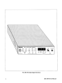
ASG 100
Audio Signal Generator
070-8546-03
Warning
The servicing instructions are for use by qualified
personnel only. To avoid personal injury, do not
perform any servicing unless you are qualified to
do so. Refer to all safety summaries prior to
performing service.
WARRANTY
Tektronix warrants that this product will be free from defects in materials and workmanship for a period of one (1)
year from the date of shipment. If any such product proves defective during this warranty period, Tektronix, at its
option, either will repair the defective product without charge for parts and labor, or will provide a replacement in
exchange for the defective product.
In order to obtain service under this warranty, Customer must notify Tektronix of the defect before the expiration
of the warranty period and make suitable arrangements for the performance of service. Customer shall be
responsible for packaging and shipping the defective product to the service center designated by Tektronix, with
shipping charges prepaid. Tektronix shall pay for the return of the product to Customer if the shipment is to a
location within the country in which the Tektronix service center is located. Customer shall be responsible for
paying all shipping charges, duties, taxes, and any other charges for products returned to any other locations.
This warranty shall not apply to any defect, failure or damage caused by improper use or improper or inadequate
maintenance and care. Tektronix shall not be obligated to furnish service under this warranty a) to repair damage
resulting from attempts by personnel other than Tektronix representatives to install, repair or service the product;
b) to repair damage resulting from improper use or connection to incompatible equipment; or c) to service a
product that has been modified or integrated with other products when the effect of such modification or
integration increases the time or difficulty of servicing the product.
THIS WARRANTY IS GIVEN BY TEKTRONIX WITH RESPECT TO THIS PRODUCT IN LIEU OF
ANY OTHER WARRANTIES, EXPRESSED OR IMPLIED. TEKTRONIX AND ITS VENDORS
DISCLAIM ANY IMPLIED WARRANTIES OF MERCHANTABILITY OR FITNESS FOR A
PARTICULAR PURPOSE. TEKTRONIX’ RESPONSIBILITY TO REPAIR OR REPLACE DEFECTIVE
PRODUCTS IS THE SOLE AND EXCLUSIVE REMEDY PROVIDED TO THE CUSTOMER FOR
BREACH OF THIS WARRANTY. TEKTRONIX AND ITS VENDORS WILL NOT BE LIABLE FOR ANY
INDIRECT, SPECIAL, INCIDENTAL, OR CONSEQUENTIAL DAMAGES IRRESPECTIVE OF
WHETHER TEKTRONIX OR THE VENDOR HAS ADVANCE NOTICE OF THE POSSIBILITY OF
SUCH DAMAGES.
4.
5.
6.
Check Amplitude Flatness (+0.05/0.2 dB, 10 Hz to 20 kHz) . . . . . . . . . . . . . . . . . . . 4–3
Check Channel-to-Channel Level Difference (≤ 0.2 dB at +14 dBu) . . . . . . . . . . . . .4–4
Check Total Harmonic Distortion + Noise (< 0.015%, 20 Hz to 19 kHz
< 0.056% > 19 kHz to 20 kHz). . . . . . . . . . . . . . . . . . . . . . . . . . . . . . . . . . . . . . . . . . . . 4–5
Digital-to-Analog Converter (Diagrams 3 and 3a) . . . . . . . . . . . . . . . . . . . . . . . . . . . . . . . . . . . . . . . 5-5
RTS and CTS are not used in the ASG 100.
Pins 4, 6, and 9 of the connector are not to
be connected to the terminal interconnection cable. Those pins are used for contact
closure remote control.
±0.2 dB, 10 Hz to 20 kHz*
+0.05/–0.2 dB, 10 Hz to 20 kHz (relative to 1 kHz)**
*
**
B039999 and below
B040000 and above
Typ. ±0.1 dB, 10 Hz to 19 kHz*
Typ. +0.05/–0.1 dB, 10 Hz to 15 kHz**
< 0.01% (–80 dB), 20 Hz to 18 kHz*;
< 0.0.25% (–72 dB), 18 kHz to 20 kHz*;
< 0.015% (–76.5 dB), 10 Hz to 19 kHz**;
< 0.056% (–65 dB), >19 kHz to 20 kHz**
*
**
B039999 and below
B040000 and above
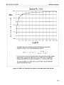
< 0.005% at 1 kHz at full output, measured
over a 22 KHz bandwidth (see typical curve
in Figure 1–1). This typical specification
will also hold at +14 dBu and +4 dBu.
0.008
%THD + Noise
(measured
over 22 kHz
bandwidth)
Noise limited –5.4
below –5.4 dB
+4.6
+14.6
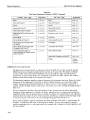
Introduction & Specifications
Table : Certifications and compliances
Category
Standards or description
EC Declaration of Conformity –
EMC
Meets intent of Directive 89/336/EEC for Electromagnetic Compatibility. Compliance was
demonstrated to the following specifications as listed in the Official Journal of the European Union:
EN 50081-1 Emissions:
EN 55022
Class B Radiated and Conducted Emissions
EN 50082-1 Immunity:
IEC 801-2
IEC 801-3
IEC 801-4
Electrostatic Discharge Immunity
RF Electromagnetic Field Immunity
Electrical Fast Transient/Burst Immunity
Must use high quality shielded cables to ensure conformance with EMC regulations.
Australia/New Zealand
Declaration of Conformity – EMC
Complies with EMC provision of Radiocommunications Act per the following standard(s):
AN/NZS 2064.1/2
Industrial, Scientific, and Medical Equipment: 1992
AN/NZS 3548
Information Technology Equipment: 1995
EMC Compliance
Meets the intent of Directive 89/336/EEC for Electromagnetic Compatibility when it is used with the
product(s) stated in the specifications table. Refer to the EMC specification published for the stated
products. May not meet the intent of the directive if used with other products.
FCC Compliance
Emissions comply with FCC Code of Federal Regulations 47, Part 15, Subpart B, Class A Limits.
EC Declaration of Conformity –
Low Voltage
Compliance was demonstrated to the following specification as listed in the Official Journal of the
European Union:
Low Voltage Directive 73/23/EEC, amended by 93/69/EEC
EN 61010-1:1993
Safety requirements for electrical equipment for measurement
control and laboratory use.
U.S. Nationally Recognized
Testing Laboratory Listing
UL3111-1
Standard for electrical measuring and test equipment.
UL1244
Standard for electrical and electronic measuring and testing
equipment.
Canadian Certification
CAN/CSA C22.2 No. 231
CSA safety requirements for electrical and electronic measuring
and test equipment.
Additional Compliance
IEC61010-1
Installation (Overvoltage)
Category
Terminals on this product may have different installation (overvoltage) category designations. The
installation categories are:
Pollution Degree
ASG100 Service Manual
Safety requirements for electrical equipment for measurement,
control, and laboratory use.
CAT III
Distribution-level mains (usually permanently connected). Equipment at this level is
typically in a fixed industrial location.
CAT II
Local-level mains (wall sockets). Equipment at this level includes appliances, portable
tools, and similar products. Equipment is usually cord-connected.
CAT I
Secondary (signal level) or battery operated circuits of electronic equipment.
A measure of the contaminates that could occur in the environment around and within a product.
Typically the internal environment inside a product is considered to be the same as the external.
Products should be used only in the environment for which they are rated.
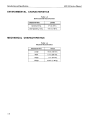
1–6a
Introduction & Specifications
Table : Certifications and compliances (cont.)
Category
1–6b
Standards or description
Pollution Degree 1
No pollution or only dry, nonconductive pollution occurs. Products in
this category are generally encapsulated, hermetically sealed, or
located in clean rooms.
Pollution Degree 2
Normally only dry, nonconductive pollution occurs. Occasionally a
temporary conductivity that is caused by condensation must be
expected. This location is a typical office/home environment.
Temporary condensation occurs only when the product is out of
service.
Pollution Degree 3
Conductive pollution, or dry, nonconductive pollution that becomes
conductive due to condensation. These are sheltered locations where
neither temperature nor humidity is controlled. The area is protected
from direct sunshine, rain, or direct wind.
Pollution Degree 4
Pollution that generates persistent conductivity through conductive
dust, rain, or snow. Typical outdoor locations.
ASG100 Service Manual
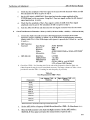
4.
CHECK AMPLITUDE FLATNESS (+0.05/–0.2 DB, 10 HZ TO 20 KHZ)
d. Check that the amplitude is flat within +0.05/–0.2 dB at each test frequency with respect to the
1000 Hz 14 dBu amplitude noted in part a. The amplitude accuracy specification permits the
14 dBu amplitude at 1000 Hz to be 3.7938 to 3.9726 V, and the flatness has to be calculated using
the measured voltage to check the actual flatness over frequency. (More or other frequencies may be
checked as considered necessary. The empty columns of Table 4–3 are provided to enter the amplitude
for each frequency if you wish.)
6.
Check Total Harmonic Distortion + Noise (< 0.015%, 20 Hz to 19 kHz; < 0.056%, > 19 kHz to 20 kHz)
*
d. Check for a THD + N of less than 0.015% for each of the frequencies listed in Table 4–4.
(Other frequencies may be used if considered necessary. The empty columns of Table 4–4 are
provided to enter the THD + N reading for each frequency if you wish.)
10000 Hz*
15000 Hz*
18000 Hz*
19000 Hz*
* Measurements above 7 kHz should be made using the 80 kHz Low Pass Filter.
0.056%.
Select the AUDIO BAND PASS filter.
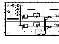
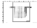
(Diagrams 3 and 3a)
The feedback circuit that sets the loop gain of the DAC and the current-to-voltage converter is formed
by resistors R24 (an adjustable potentiometer) and R23.
The signal voltage from U20 is applied to FL3, an 11-pole, low-pass filter with a 23 kHz cutoff. The upper
output signal frequency is 20 kHz, but a 23 kHz low-pass filter is used to move the ripple effect of the
filter above 20 kHz.
The DAC sends a new output every 1/(48 kHz), which approximates a sine wave. The filter smooths the
steps to a sine wave.
The signal then enters buffer amplifier U13A. The buffer has a gain of four to compensate for a 6 dB
loss in the filter and to provide the proper operating amplitude. At TP7 the signal is twice the amplitude
as it is at U20 pin 10.
A2
A2
671–1758–08
671–1758–09
307–0793–00
B031761
B040000
B031760
B039999
CIRCUIT BD ASSY:MAIN
CIRCUIT BD ASSY:MAIN
80009
80009
671–1758–08
671–1758–09
A2
671–1758–08
B031761
A2
671–1758–09
B040000
B031760
B039999
CIRCUIT BD ASSY:MAIN
80009
671–1758–08
CIRCUIT BD ASSY:MAIN
80009
671–1758–09
A2C137
281–0775–02
CAP,FXD,CER:MLC;0.1UF,20%,50V,X7R,0.265
04222
SA205C104MAA
04222
SA205C104MAA
0.100;AXIAL,T&R
A2C138
281–0775–02
671–1758–04
CAP,FXD,CER:MLC;0.1UF,20%,50V,X7R,0.265
0.100;AXIAL,T&R
A2FL2
119–4080–00
671–1758–00
A2FL2
671–4081–00
671–1758–09
A2FL3
119–4080–00
671–1758–00
A2FL3
671–4081–00
671–1758–09
671–1758–08
671–1758–08
FILTER,LOWPASS
80009
FILTER,LOWPASS
80009
119–4080–00
671–4081–00
FILTER,LOWPASS
80009
119–4080–00
FILTER,LOWPASS
80009
671–4081–00
A2R20
A2R20
A2R21
A2R22
A2R22
A2R23
A2R23
A2R24
A2R25
A2R25
322–3222–07
322–3176–00
322–3222–07
322–3222–07
322–3176–00
322–3001–00
322–3201–00
311–1895–00
322–3001–00
322–3201–00
671–1758–00
671–1758–08
671–1758–00
671–1758–08
671–1758–00
671–1758–09
671–1758–08
671–1758–00
671–1758–09
671–1758–00
671–1758–09
671–1758–08
671–1758–00
671–1758–09
671–1758–08
671–1758–08
RES,FXD,FILM:2K OHM,0.1%,0.2W TC=T9
RES,FXD,FILM:665 OHM,0.1%,0.2W TC=T0MI
RES,FXD,FILM:2K OHM,0.1%,0.2W TC=T9
RES,FXD,FILM:2K OHM,0.1%,0.2W TC=T9
RES,FXD,FILM:665 OHM,0.1%,0.2W TC=T0MI
RES,FXD,META FILM:10 OHM,0.1%,0.2W TC=100
RES,FXD,META FILM:1.21K OHM,0.1%,0.2W TC=T9
RES,VAR,NONWW:TRMR2K OHM,10%,0.5,LIN
RES,FXD,META FILM:10 OHM,0.1%,0.2W TC=100
RES,FXD,META FILM:1.21K OHM,0.1%,0.2W TC=T9
80009
80009
80009
80009
80009
80009
80009
32997
80009
80009
322–3222–07
322–3176–00
322–3222–07
322–3222–07
322–3176–00
322–3001–00
322–3201–00
3299W–1–202
322–3001–00
322–3201–00
671–1758–00
A2U1
156–6157–01
671–1758–08
671–1758–07
DSP56001 ON ADAPTER
C135
C136
C136
C200
283–0067–00
283–0067–00
283–0067–00
283–0067–00
B040000
B010100
B040000
B010410
E200
276–0647–00
B010410
B010409
B039999
CAP,FXD,CER D1:0.001UF,10%,200V
CAP,FXD,CER D1:0.001UF,10%,200V
CAP,FXD,CER D1:0.001UF,10%,200V
CAP,FXD,CER D1:0.001UF,10%,200V
51046
51046
51046
51046
283–0067–00
283–0067–00
283–0067–00
283–0067–00
CORE,EM:TOROID,FERRITE
78488
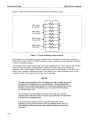
57–0126
REMOTE
PORT
REAR PANEL
<8> SERIAL
FILTER
<7> FRONT PANEL
RS232C
Power Supply
(120/240 V)
+15 V
–15 V
+5 V
Chip
Selects
PAL
Front Panel
Processor
(8751)
LEDs
EPROM
64K x 8 BIT
Display
Buttons
Front Panel
Interface
50-Pin
Connector
RAM
8K x 8 BIT
DIP
SWITCH
<1> CONTROL PROCESSOR
<5> HEADPHONE
AMPLIFIER
<2> DIGITAL SIGNAL
PROCESSOR
Battery
Backup
>
Volume
Headphone
Amplifier
PAL
Host
Port
Phones
Left
Chip Selects
EPROM
64K x 24 BIT
RAM
8K x 8 BIT
Control
Register
Control
Lines
Phones
Right
Headphone
Amplifier
DSP
(56001)
DSP Bus
Serial
Port
0-50 dB
Left D/A
Converter
Codec
Low-Pass
Filter
Left Step
Attenuator
Audio
Out Left
Mono
Data Formatter/
Synchronizer
MIC
0-50 dB
Preamp
and AGC
<6>MICROPHONE
PREAMP
Right D/A
Converter
<3>DIGITAL TO
ANALOG CONVERTER
Low-Pass
Filter
Output Buffers
0–10 dB Gain
Right Step
Attenuator
<4> CH 1 AND CH 2
GAIN/ATTENUATOR
Audio
In Left
Audio
Out right
Audio
In Right
REAR PANEL
KEY
SIGNAL LINE
CONTROL LINE
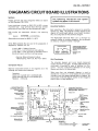
SCHEMATIC DIAGRAM
NUMBER
<n>
ASG 100 Block Diagram
ASG 100
Static Sensitive Devices
See Maintenance Section
A2 MAIN BOARD
671-1758-04 & UP
Schematic Diagram <1> Component Locator Chart
Main Board, Assembly A2. Partial Assembly A2 also shown on Diagrams 2, 3, 4, 5, and 6.
BLOCK DIAGRAM
C71
C72
C77 *
C78
C103
C109
C110
C111
B3
B3
B4
B4
G2
K7
L7
L6
K5
N5
C115
B3
L6
F4
B5
B5
M3
L5
M5
CR14 *
B4
K6
J8
J25
J26
J28
J29
H1
C5
A3
A1
B3
N5
J4
K7
J7
L5
R148
R149
R153 *
R154 *
R158
C1
B3
B4
B4
A2
L6
L7
L5
L5
K7
R162
R174
G2
H1
N6
N5
R177
R178
R179
R189
B1
B1
A3
B3
J7
J7
K7
L6
U40E
U40F
U47
D3
D3
D2
G4
G4
L6
S1
A1
J8
U40B
U40C
D3
B3
G4
G4
U48
U49
U50
U51
U52
B2
E2
G3
G5
G4
J7
L6
L7
L8
L7
U54
U55 *
U62
U63
U64
U67
C4
B4
E4
F4
F3
B5
K6
K6
M2
M5
M4
K5
Y2
B2
K8
*See parts
list for earlier values
and serial
number
ranges.
)
"%
'&'
"!,
%
%
"
&
"
(
(
%
(
'
#%"
#%"
#%"
#%"
#%"
#%"
&%
%+
'+
!'"
%'&
'&
%
*%
%
!'
(
,
2
)
0
%
#
#
#
#
#
#
#
#
#%+
#
'+
#!'"
#!'
#'
#'
#*%
#%
#
#
#
#
#
#
#
#
)
!
+'
+'
0
%&'
(
&
(
)
'
'
'
'
'
'
'
'
'
'
'
'
'
'
'
'
%
(
&
$
$
$
$
$
$
$
$
%
%
%
%
%
%
%
%
%
%
%
%
%
%
%
%
)
)
(/)
%
*
1
%
!
"
%-.
(
#%"
#&!
)##
%&'
%
#
#
#
#
#
#
#
#
%-.
'-.
%
)
!'%!
#%"
'-.
)
DIP
SWITCH
FRONT PANEL PROCESSOR
)
%
%
%
%
%
%
%
%
%&'
#&!
%
*%
%
%
%
%
%
%
*%
#!
#!
%&'
&*
&*
&*
&*
&*
&*
&*
&*
&*
&*
&*
&*
&*
&*
)
(
#)
&*!
&*
!
#!
#!
&#!
&#%&'
%" !)%
&#*%
"
"
"
"
"
"
"
"
"
"
(
(
&#!
&#%&'
&#*%
(
FRONT
PANEL
INTERFACE
RAM
'
'
'
'
'
'
'
'
%"!'
#!
"%
)
)
%
+'%&'
+'%&'
(
BATTERY
BACKUP
&
1
(
&
(
!)%
&
)
)
"*
%
%
(
)
!"%"(!
'%"(!
&#%'&&'"%
%%)(&!
&%!( %%!&
%'&
'+
'%
&%
%+
'&
%
1
'"
'"
'"
%"
%"
%"
%"
%"
%
%
%
%
%
!
)
)
!
1
(
+
#
#"
)"('
*
)''
)
!
%&'
)
!
%'&
'+
'%
&%
%+
'&
%
)
)
1
(
&%
'%
"%
)
"
*%
%
'
'
'"
)
!
)"
(
*
"
)
!
'
'
'
'
'
'
'
'
&*!
%&'
1
%
%
%
%
%
%
%
%
%
%
%
%
%
%
%
%
%
%" #&!
(
'
'
'
'
'
'
'
'
%&'
'
'
'
'
'
'
'
'
)
(
&
$
$
$
$
$
$
$
$
'%
%
%&'
RS232 PORT
(
+
'
'
'
(
%
''
(
&
%
%
%
%
%
%
%
%
%
%
%
%
%
%
%
(
&
,
,
,
,
,
,
,
,
)
!
&*
&*
&*
&*
&*
&*
&*
&*
&*!
")##
'
'
'
'
'
'
'
'
'
'
'
'
'
'
'
'
)
(
&
,
,
,
,
,
,
,
,
)
!
&*
&*
&*
&*
&*
&*
#%"
#%"
&*
!
EPROM
#" !"%
&
"!'%"#%"&&"%
ASG 100
Static Sensitive Devices
See Maintenance Section
Back of board.
A2 MAIN BOARD
671-1758-00 – 03
Schematic Diagram <2> Component Locator Chart
Assembly A2. Partial Assembly A2 also shown on Diagrams 1, 3, 4, 5, and 6.
BT1
E5
L2
J31B
J32
H1
B5
L1
L1
R159
R190 *
C93
C114
E5
G5
I4
L1
CR15 *
F5
M1
J30
J31A
B1
H2
K8
L1
R1
R2
R3
R5
R6
R7
D1
D1
D1
B2
E5
D5
J3
J3
J3
L4
I4
I5
U1
U2
U3
U4
U5
U6
E5
A3
J4
M1
B1
G2
G3
G3
F5
G5
L4
K1
J1
I1
M2
L1
U9
U10
U11
U12
U40D
E5
E2
E2
D3
C5
I5
J6
J6
M3
G4
W5 *
A3
I4
Y3
A3
I3
*See parts
list for earlier
values and
serial number ranges.
&,-
&,'
(
$,
-
$,
'
$
$
$
'
'
$
%")$
%" &
(
%
%
'
&
&
&
&
&
&
&
&
)$
%" &
$
$*
&*
%
%
%
&
%
%$
%&
!
!
%"$%&
(
+
0
(
)
$
(
!$
&%&
! +
'
%"#"
"
"
"
"
"
"
"
"
"
"
"
"$)
"
"$#
"
"$*
"&*
"
%
"%
"%
"%
"%
"%$
"%&
!$#
!$#
$%&
*&
*&
$
(
(
(
(
(
(
(
(
(
(
"%
%
$
)$
*+
$
(
"%
%
*+
$
)$
*&
*&
*&
$
(
(
$
&$
%"$%&
&$
%"$%&
'
%
#
#
#
#
#
#
#
#
&$,
&$,'
&$
&$
&$
&$
&$
&$
&$
&$
CONTROL
REGISTER
$
'
%
#
#
#
#
#
#
#
#
&$
%
%
&
"%
%
&$
)$
*+
DSP
&$
&$
&$
&$
&$
&$
&$
&$
$
'
"
(
!
!
!
!
!
!
!
!
!
!
!
&$
"
*&
*&
*&
$!
$
$!
$
$!
$
$!
$
)$
!
$
'
!(""
'
$*
&*
%
*&$%&
!$
&%&
'&'$
*" %!
!(""
'
'
"
EPROM
"%
%
$
)$
*+
!(""
*&$%&
'
$
.
'
%
!$!' &$!' %&$"$&%%&
!$$$('% %$ '$$ %
$*
&*
%
%
%
&
%
%$
%&
%"$%&
CODEC
(
$
"$"
!$
&%&
! +
'
%
"
$
'
%
(
'
%&
'
(*
&%*
%*
$
$
%$
"
%*
*
")$!
")$!
(
(
BATTERY
BACKUP
$
%$
$
$
(
(
&
(
'
%
$
(
!
&
&
&!
(
(!
)
!
RAM
(
(!
&&
'
/
"!
!$
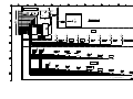
ASG 100
DIGITAL SIGNAL PROCESSOR
–
ASG 100
Schematic Diagram <3>
Component Locator Chart
Main Board, Assembly A2.
Partial Assembly A2 also shown on Diagrams 1, 2, 4, 5, and 6.
C21
C22
C23
C24
C31
F3
F3
H4
E3
F4
G7
G6
G6
I5
G7
C32
C34
C94
C95
C116
F4
E4
E4
E3
E4
G6
I6
I6
I5
I6
C117
C118
C119
C120
C121
E2
E5
E5
F5
F5
H4
H7
G4
G5
H7
FL2
FL3
F3
F4
G5
G5
J2
C1
I7
R14
R15
R16
R17
C3
C4
C3
C4
H5
H6
H6
H7
R19
R20
R21
R22
H2
G2
H4
G4
F6
F6
F7
F7
R23
R24
R25
R26
R27
E3
E4
E2
E2
C4
H6
H6
H5
H5
H6
R28
R66 *
R160
R161
C3
B1
E4
E3
H5
TP7
TP8
H4
H3
F7
G6
U13A
U13B
U14
U15
U16
H4
H3
C4
C2
B1
F7
F7
I6
I5
I7
U17
U18
U19
U20
U21
B1
B2
B2
E4
E3
H7
I6
I5
I6
I4
U66A
U66B
U69
U70
B1
A1
E5
E5
I4
I4
G5
H7
H6
H5
*See parts list for earlier values and serial
number ranges.
*
)
'
)
)
'(
$! )
'
$
&
%
%
*
%
%
%
%
%
%
%
%
)
*
&
(
(
&
*
*
*
)
'
%
%
%
%
%
%
%
%
&
LEFT D/A CONVERTER
*
*
%
%
)
'
)
$
&
*
%
%
%
%
%
%
%
%
'
*
&
LEFT LOW PASS FILTER
&
*
*
'
)
$! *
)
'
%
%
%
%
%
%
%
%
&
&
*
*
$! $! &
)
"
* "
* *'
"
*'
(
"
(&!
*
*
&
,
*#)(
-
&
DATA FORMATTER/SYNCHRONIZER
&
&
*
!'
'
&
#)(
"
,
)
-
*
#+$'' (&
"
#)(
*
"
"
"
*
($
)
!'
-
&
*
&
&
*
*
$! )
$! $! &
)
"
* "
* *'
"
*'
(
"
(&!
#)(
*
*#)(
*
&
,
-
&
*
&
&
*
!'
'
&
"
,
)
-
*
#+$'' (&
"
#)(
*
"
"
"
*
)
($
-
*
!'
-
&
*
)
*
-
RIGHT D/A CONVERTER
-
" #&#)"
( &#)"
-
RIGHT LOW PASS FILTER
-
*
)
ASG 100
"#(
'$&(' '(#&& &* )'
"'& ")!&&"'
DIGITAL TO ANALOG CONVERTER
#*
$#!"#&
ASG 100
Schematic Diagram <3a>
Component Locator Chart
Main Board, Assembly A2.
Partial Assembly A2 also shown on Diagrams 1, 2, 4, 5, and 6.
C21
C22
C23
C24
C31
F3
F3
H4
E3
F4
G7
G6
G6
I5
G7
R22
G4
F7
C32
C34
C94
C95
C116
F4
E4
E4
E3
E4
G6
I6
I6
I5
I6
R23
R24
R25
R26
R27
E3
E4
E2
E2
C4
H6
H6
H5
H5
H6
R28
R66 *
R160
R161
C3
B1
E4
E3
H5
C117
C118
C119
C120
C121
E2
E5
E5
F5
F5
H4
H7
G4
G5
H7
TP7
TP8
H4
H3
F7
G6
FL2
FL3
F3
F4
G5
G5
U13A
U13B
U14
U15
U16
H4
H3
C4
C2
B1
F7
F7
I6
I5
I7
J2
C1
I7
R13
R14
R15
R16
R17
G3
C3
C4
C3
C4
G6
H5
H6
H6
H7
U17
U18
U19
U20
U21
B1
B2
B2
E4
E3
H7
I6
I5
I6
I4
R18
R19
R20
R21
G4
H2
G2
H4
F7
F6
F6
F7
U66A
U66B
U69
U70
B1
A1
E5
E5
I4
I4
G5
H7
H6
H5
*See parts list for earlier values and serial
number ranges.
*
)
'
)
)
'(
$! $
&
%
%
*
)
'
%
%
%
%
%
%
%
%
)
*
&
(
(
&
*
*
*
)
'
%
%
%
%
%
%
%
%
&
LEFT D/A CONVERTER
*
*
)
$
&
%
%
*
)
'
%
%
%
%
%
%
%
%
'
*
&
LEFT LOW PASS FILTER
&
*
*
'
)
$! *
)
'
%
%
%
%
%
%
%
%
&
&
*
*
$! $! &
)
"
* "
* *'
"
*'
(
"
(&!
#)(
*
*
-
*#)(
&
.
&
DATA FORMATTER/SYNCHRONIZER
&
&
*
!'
'
&
"
-
)
.
*
#+$'' (&
"
#)(
*
"
"
"
*
($
)
&
!'
.
&
*
&
&
*
*
$! )
$! $! &
)
"
* "
* *'
"
*'
(
"
(&!
#)(
*
*#)(
*
&
-
.
&
*
&
&
*
!'
'
&
"
-
)
.
*
#+$'' (&
"
#)(
*
"
"
"
*
)
&
($
.
*
!'
.
&
*
)
*
.
RIGHT D/A CONVERTER
.
" #&#)"
( &#)"
.
RIGHT LOW PASS FILTER
.
*
)
ASG 100
"#(
'$&(' '(#&& &* )'
"'& ")!&&"'
DIGITAL TO ANALOG CONVERTER
#+
$#!"#&
,
ASG 100
Schematic Diagram <4> Component Locator Chart
Main Board, Assembly A2.
Partial Assembly A2 also shown on Diagrams 1, 2, 3, 5, and 6.
C35
C36
C37
C38
C96
D1
D2
D4
D4
D1
D5
D5
D7
D8
D5
FL11 *
H4
A5
C97
C98
C99
C126 *
C127 *
B1
D3
B4
H1
H1
D6
D7
D7
A6
A6
J11
J12
J13
J14
J33
H1
H2
H3
H4
H5
A6
A4
A7
A5
D5
K2A
K2B
K2C
G5
G5
G4
B5
B5
B5
C128 *
C129 *
C130 *
C131 *
C132 *
H1
H1
H3
H4
H4
A4
A4
A8
A8
A5
K5A
K5B
K5C
G3
G2
G1
B4
B4
B4
C133 *
C137
C138 *
C139 *
C140 *
H4
F4
G5
G3
G3
A5
H4
B5
B4
B4
L1 *
L2 *
L3 *
C3
C5
G3
C141 *
C143 *
C2
C4
D5
D6
Q2
Q3
Q4
Q5
Q6
CR4
CR5
CR6
CR7
D1
D2
E2
E2
C5
C5
C6
C6
CR8
CR9
CR10
CR11
D4
D4
E4
E5
C7
C7
C8
C8
FL4 *
FL5 *
FL6 *
FL7 *
H1
H1
H2
H2
A6
B6
A5
A5
FL8 *
FL9 *
FL10 *
H3
H3
H4
A7
B7
A6
R33
B2
D6
R34
R35
R36
R37
R38
B2
B2
B3
D1
D2
D6
E6
E6
C4
C5
R39
R40
R41
R42
R43
E2
E1
E2
E3
F2
B5
B4
C5
C6
B6
H4
B7
B7
R44
R45
R46
R67
R68
F2
E2
E2
B1
B1
B5
C5
C5
D6
D6
D1
D2
D1
D2
F2
C5
C5
C4
C5
C5
R69
R70
R71
R72
R73
B4
B4
B4
B4
B4
D7
D7
D7
D7
D8
Q7
Q8
Q9
Q10
Q11
F2
F2
F3
D4
D4
C6
B5
B6
C6
C7
R74
R75
R76
R77
R78
B5
B5
B5
D4
D4
D8
E8
E8
C6
C7
Q12
Q13
Q14
Q15
Q16
D4
D4
F4
F5
F4
B6
B7
C7
C8
B7
R79
R80
R81
R82
R83
E4
E4
E4
E5
F5
B7
B6
C7
C8
B7
Q17
Q20 *
F5
G4
B7
N1
R29
R30
R31
R32
B2
B2
B2
B2
D6
D6
D6
D6
R84
R85
R86
R107
R108
F5
E4
E4
B3
B3
B7
C7
C7
D7
D7
*See parts list for earlier values and serial number ranges.
R167A
R167B
R167C
R167D
R167E
F1
F2
F2
F2
F5
B6
B6
B6
B6
B6
R167F
R167G
R167H
R168
R173
F5
F4
F4
F1
E3
B6
B6
B6
B4
C4
R180
R181
R182
R183
R184
B3
B3
B3
B5
B5
E7
D6
D7
D8
D8
R185
R191 *
B5
G4
E8
N1
U22
U23A
U23B
U25A
U25B
C1
D2
E2
C1
C3
E5
C5
C5
C6
C6
U25C
U25D
U27
U28
U29A
U29B
D3
D1
E1
C4
D4
E5
C6
C6
G8
E7
C7
C7
C135 *
C136 *
C200 *
H3
H3
H3
––
––
––
E200 *
H3
––
CHASSIS
&$,-
&$,-
'
'
(
$
(
&$
&$
&$
.0
'
0
$
$
'
'*
(
(
(
'
"$()
$
/
#
"$(
$
$
$
0
$
#
$
(
(
LEFT
STEP
ATTENUATOR
$
#
'
$
$
'!
!'&
&
!'&"'&
"!
#
LEFT OUTPUT BUFFER
(
#
0
$
(
0
0
$
'
$
$
&$
&$
&$
$
%
%
%
%
%
%
%
%
(
(
(
(
!'&
$
/
"$(
$
'
$
$
0
$
#
$
(
(
'!
!'&
$&
!'&"'&
!'&
"'&
$
(
/
(
'!
$&
!'&
#
$
"!
$
/
$
$
$
(
$
/
#
$
#
0
(
/
!&&%$ &)!$%&'+
" $ %!&
$'%$
$
(
(
/
'
'*
$
.
(
'
.
&$
$
0
$
#
$
$
$
RIGHT
STEP
ATTENUATOR
$
#
$
'
$
$
RIGHT OUTPUT BUFFER
#
$
(
"!
$
$
0
!'&
#
(
$
$
$
0
"!
(
$
(
&$
&$
$
ASG 100
$
(
"! !$
$
$
$
%&$"$&%%&
!$$$('% %$ '$$ %
!'&
$
$
&$!' "'&
$
$
'!
&
#
!$!' /
$
$
(
(
!'&
$
"!
$
$
$
! !
#
$
/
'
$
0
!&$ " %!&
$&(
(
'
/
!& " %!&
$%"$
$
$
#
/
!&
%
%%% $
!'&
(
0
(
&$
(
(
%
%
%
%
%
%
%
%
(
"
/
.
(
'
$
&$
'
.
&$
&$
&$
&$
"!
!'&
'$
!$
CHANNEL 1 AND CHANNEL 2 GAIN / ATTENUATOR
ASG 100
Schematic Diagram <5>
Component Locator Chart
Main Board, Assembly A2.
Partial Assembly A2 also shown on Diagrams 1, 2, 3, 4, and 6.
C39
C40
C41
C42
C43
D3
E3
F3
C1
C1
F4
G4
G4
G5
E4
C45
C46
C47
C48
C49
D4
E4
F4
C2
C2
F5
F5
F5
G6
E6
C51
C100
C101
C135
C136
C200
C5
B2
B1
BH
BH
CH
E4
F6
F5
E200
BH
J20
J200
H3
BH
L1
Q18
Q19
C3
C3
D5
C4
R109
R110
R111
R112
R113
G3
F3
D3
C1
F3
G4
F4
F4
F4
G4
R114
R115
R117
R118
F3
B1
B1
G4
G4
F5
F5
G5
R119
F4
F5
R120
R121
R122
R123
R124
D4
C2
F4
F4
B2
E5
E5
F5
G5
F6
R126
R127
R128
R129
R130
B2
E4
E4
E3
E3
F6
F5
F5
F4
F4
R132
R133
R163
R164
R165
B5
B5
B1
B1
B2
E4
E4
F5
F5
F6
R166
R175
R176
R186
R187
B2
B3
B3
C3
C3
F6
E5
D5
D4
D5
U33
U35A
U35B
U36
U38A
E3
B1
F3
E4
B2
F4
F5
F5
E5
F6
U38B
U39
U40A
U41
F4
C5
B3
D3
F6
E4
G4
D5
*See parts list for earlier values and serial
number ranges.
1
$#
$#
&
&
*
&
)
3
&
&
#+
3
$#"'
!#)"(#"
&#"('("
*
HEADPHONE AMPLIFIER
1
$#
$#
&
&
*
&
(&)
)
3
&
&
$#"'
!#)"(#"
&#"('("
3
*
1
*
)
'
)
$&*+
&
$&*
&
$&*
"02/
$2.4
&
3
)
&
*
*
&
1
&
*
"
"
'
'
'
'(
"#($"#"#(
"'&(#"
)
,
#)(
&
&
&
$#
&$#
)
&
( & ' *
&
%
&
$#"'
!#)"(#"
&#"('("
*
%
&
1
*
3
&
1
&
)
,
*
"
"
'
'
'
'(
#)(
&
&
&
)
&
&
*
*
)- *
&
&
&'(
&
)
3
%
*"
)
*
' (& $&(' '(
#&& &* )'"
'& ")!&&"'
" #&#)"
( &#)"
$#!"#&
ASG 100
HEADPHONE AMPLIFIER
ASG 100
Schematic Diagram <6>
Component Locator Chart
Main Board, Assembly A2.
Partial Assembly A2 also shown on Diagrams 1, 2, 3, 4, and 5.
C3
C4
C5
C6
C7
D3
D5
D3
D5
D3
H4
I4
H4
I4
I1
C8
C9
C11
C12
C13
D3
E3
E3
E3
E3
K1
J1
M2
L3
I5
C14
C15
C16
C25
C26
F3
F3
F3
E5
E3
M3
J6
J5
H7
H7
C27
C28
C29
C30
C52
E5
E3
E5
E3
G2
H6
H6
H7
H5
F7
C53
C54
C55
C56
C57
C2
B2
G2
C2
C2
E7
E6
F7
F7
F7
C59
C60
C61
C62
C63
F1
F2
F1
D2
D2
F8
G7
E8
G8
G8
C64
C65
C66
C67
C68
E2
D2
E2
B3
B5
G7
G8
G7
I2
I3
C69
C70
C79
C80
C81
B3
G2
D4
D4
D4
I2
F8
J6
L6
L7
C82
C83
C84
C85
C86
E4
E4
E4
E4
F4
L7
L6
L5
K5
I6
C87
C88
C89
F3
G3
G3
K3
K4
L3
C102
C105
G1
F4
E7
M2
C106
C108
C112
C113
C124
F4
C3
C3
C3
D4
M4
H1
M5
M5
H1
C125
C134
C137
C142 *
D4
D4
F4
B3
K5
N8
H4
F7
DS1
C4
H1
J7
J23
B2
B4
F6
H2
R134
R135
R136
R137
R138
C2
C2
B2
B2
C2
F7
F7
F6
F6
F7
R140
R141
R142
R143
R144
F1
F2
F1
G1
D2
F8
G7
F8
F8
G8
R145
R188
E2
C3
G8
I1
TP1
TP2
TP3
C4
C4
C4
B6
E7
G4
TP4
TP5
TP6
E4
E4
C4
L2
L8
H7
U7
U8
U42A
D3
D5
F2
H4
H4
F7
U42B
U46A
U68
C2
E2
C3
F7
G7
M5
VR3
VR4
VR5
B2
G1
G2
F6
G7
G7
W1
W123 *
E4
D4
B8
B4
*See parts list for earlier values and serial
number ranges.
MIC
PREAMP AND AGC
7
$
$
;
(
$
$"!&
#!
"$
$
($
(
;
7
;
;
($
(
(
$
;
$
$
;
$
;
$
$
;
'
;
;
'
!
!
"'&
$
&&#
;
(
!
#$ #
;
'
$
;
$#
&&$
&$&$
(849
$!
($
(
(
(
;
(
;
'
'
'
;
(
;
;
;
;
;
(
;
;
;
$
;
;
;
;
;
;
;
;
;
;
;
;
;
;
;
;
;
;
;
;
;
(
(
;
%
;
POWER DISTRIBUTION AND DECOUPLING
655.,::6%%%+:
25-2,+:.-46;5:250163.9
#")$%'##*
&#
&#
&#
&#
&#
&#
&#
&#
)
;
!
&#
&#
;
&#
&#
&129.5-6/8.929:6829,655.,:.:6,1+9929086;5-+:4:0163.
)
!"&
+5
:2.:60.:1.8
653<+::12965.7625:
9:+8086;5-
!"$"'!
&$"'!
%&$#$&%%&
"$$$('%!
%$!' $$!%
;
;
;
;
;
;
(
'
(
#"
!"$
ASG 100
MICROPHONE PREAMP AND POWER DISTRIBUTION
ASG 100
R5
J1
J2
R7
U1
C3
S1
S2
S3
S4
S5
C1
S6
C2
R3
DS1
Static Sensitive Devices
See Maintenance Section
R1
S14
R4
R2
S11
S12
S7
S8
S9
S10
DS2
S13
A1 FRONT PANEL BOARD
Schematic Diagram <7>
Component Locator Chart
Front Panel Board, Assembly A1
C1
C2
C3
C1
C1
B1
D1
G1
D1
DS1
DS2
G3
C1
A2
G2
S1A
S1B
S2A
S2B
S3A
C4
C3
D4
D3
E4
A1
A1
B1
B1
B1
J1
J2
A1
D2
D1
A1
R1
R2
R3A
R3B
R3C
B3
C4
G3
G3
F3
C2
C2
B2
B2
B2
S3B
S4A
S4B
S5A
S5B
D3
E4
E3
F4
F3
B1
C1
C1
C1
C1
R3D
R3E
R3F
R3G
R4
E3
E3
D3
C3
B3
B2
B2
B2
B2
E1
S6A
S6B
S7
S8
S9
G4
F3
C5
D5
E5
D1
D1
E2
E2
F2
R5
R6
R7
B1
C1
B1
G1
H2
D1
S10
S11
S12
S13
S14
E5
F5
G5
G5
H5
F2
D2
D2
G2
C2
U1
B2
E2
*See parts list for earlier values and serial
number ranges.
R6
VOLUME CONTROL
!
"%
)
.
%
%
)"( *
%
%
%
%
%
%
*%
#!
#!
%&'
.
.
'
'
'
'
'
'
'
'
&*
&*
&*
&*
&*
&*
&*
&*
&*
&*
&*
&*
&*
&*
#"*%
&
%
!
"%
%
*%
#!
#!
%&'
%
%
%
%
%
'
'
'
'
'
'
'
'
)
(
&#
%
*%
%&'
%"#"!
)
&&
&&
&&
!
!
&
&!
!
LEDS
)
)
)
)
)
)
%
DISPLAY
%
%
&
%
%
&
('"
%"%
)
%
&
)"
%"%
%
&
&!
"!!
%
&
)
MICROPHONE
&
!(#
!(
"('#('
&
,
-)% &
)
"!!
%
)"
&!
&
&*
%"%
&*
&
&*
('"
&
&*
!(#
&
!(
&
&*
&*
&
)
%
&*
&*
&*
&*
&*
BUTTONS
(#
&
"*!
&
'
&
%'
#(&('"
&
%$(!+
&
#'(
&
&*
&)
&
&*
!''"!
&
&*
")
!"'
ASG 100
&#%'&&'"%%%)(&
!&%!( %%!&
%"!'#!"%
FRONT PANEL
ASG 100
Static Sensitive Devices
See Maintenance Section
A4 SERIAL FILTER BOARD
Schematic Diagram <8>
Component Locator Chart
Serial Filter Board, Assembly A2A1
C1
C2
C3
C4
C5
D2
E2
D2
E2
D2
A2
A1
B2
B1
A2
C16
C17
C18
D4
D4
E4
A1
A2
A1
C6
C7
C8
C9
C10
E2
D3
E3
D3
E3
A1
B2
B1
A2
A1
FL1
FLS
FL3
FL4
FL5
D2
D2
D2
D3
D3
A1
B1
A1
B1
A1
C11
C12
C13
C14
C15
D3
E3
D4
E4
D4
A2
A1
A2
A1
A2
FL6
FL7
FL8
FL9
D3
D4
D4
D4
A1
A1
A1
A1
J1
J2
B2
F2
A2
A1
*See parts list for earlier values and serial
number ranges.
ASG 100
SERIAL FILTER BOARD
–23
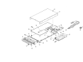
211–0722–00
B010100
B032106
B032105
1
214–3903–01
–27
–27
200–3869–01
200–3869–02
SCREW,MACHINE:6–32 X 0.250,PNH,STL,CDPL
SCREW,JACK:4–40 X 0.312 EXT THD, 4–40 INT THD,
0.188 HEX,STEEL,CAD PLATE
B010100
B031904
B032106
B031903
B032105
1
1
COVER,BOTTOM,ALUMINUM,ASG100
COVER,BOTTOM,ALUMINUM,ASG100
80009
80009
200–3869–01
200–3869–02
070–8152–0X
070–8546–0X
070–8152–0X
070–8546–0X