1
INSTRUCTION
IAi8/tA"%H
DUAL TRACE
AMPLIFIER
7A18
7A18
TABLE OF CONTENTS
SECTION 1
SPECIFICATION
lntroduction
Electrical Characteristics
7A18 And Mainframe Frequency
Response
Environmental Characteristics
Physical Characteristics
Page
OPTION INFORMATION
I- I
1-1
SECTION 6
Abbreviations and Symbols
1-3
1-3
1-3
Parts Ordering lnformation
SECTION 7
SECTION 2
SECTION 3
OPERATING INSTRUCTIONS
DIAGRAMS AND CIRCUIT BOARD
ILLUSTRATIONS
Installation
2-1
Front Panel Controls and Connectors
2-1
General Operating Information
2-2
Basic Applications
2-4
Symbols and Reference Designators
Voltage and Waveform Conditions
CIRCUIT DESCRiPTlON
SEC'TION 8
Introduction
Block Diagram Description
Detailed Circuit Description
SECTION 4
ELECTRICAL PARTS LIST
3-1
3-1
MECHANICAL PAR1'S LIST
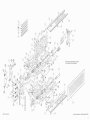
Mechanical Parts List Information
Index of Mechanical Parts Illustrations
Mechanical Parts List
3-1
MAINTENANCE
Accessories
Preventive Maintenance
Troubleshooting
SECTION 5
Replacement Parts
4-3
Component Replacement
4-4
CALIBRATION
Recalibration Interval
CHANGE INFORMATION
Abbreviations and symbols used i n this manual are based on
5-1
or taken directly from IEEE Standard 260 "Standard
'Test Equipment Required
5-1
Symbols for Units", MIL-STD-12B and other standards o f .
Part I -.-Performance Check
5-3
the electronics industry. Change information, if any, i s
Part I I - Adjustment
5-7
located at the rear of this manual.
REV. JUNE 1974
7A18
7A18
Change information, i f any, affecting this section will be found at the rear of the manual.
t ntroduction
The 7A18 and 7A18N Dual Trace Amplifier plug-in
units are designed for use with l-ektronix 7000-Series
Oscilloscopes. The 7A18 and 7A18N are electrically identical except that readout encoding capabilities and an
"IDENTIFY" function are provided only in the 7A18. All
references made t o the 7A18 apply equally t o the 7A18N
unless othewise noted. The 7A18 is a dual-channel,
medium-bandwidth amplifier. Internal gain and compensation circuits are automatically switched to correspond to
the setting of the VOL-I"S/DIV switch. Channel 2 can be
inverted for differential measurements. The 7A18 can be
operated in any plug-in compartment of the 7000-Series
Oscilloscopes.
The following electrical characteristics are valid over the
stated environmental range for instruments calibrated at an
ambient temperature of i - 2 0 " ~to +30°c, and after a five
minute warmup unless otherwise noted.
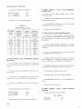
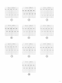
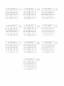
TABLE 1-1
ELECTRICAL
i wrViDiv t o 5 VIDIV; tcrt step5 111
6
I,
Deflectran Factor Accuracy
Vrrhrri 296 with GAlN adjusted a t
0 mV/Div,
Uncalibrated
:ontinuously vat iablc between cal~brart
teps; extends deflection factor tn at
East 12.5 ViDiv
(VARIABLE)
GAlN
Pern-ritsadjustrrrcnt of tic:flect~nnfactor
for cdlrbrdted or>erdtiot~
wit17 all 7000set rcs uscrltuzcopes,
-
--
Frequency Respar7se
Syslorn Dependent
(8dtv refc~encestgnal)
Upper Bandwrritlr
DC {Direct) CuuplecJ
ower ljandwiclth
-
7A18
Specification-7A1817AI 8N
TABLE 1-1(contj
Characteristic
-Information
Supplemental
Performance Requiremen_t-.- - - - --
""
Maximum Input Voltage
DC Coupled
!50 volts, (DC + Peak AC); AC comIonent 500 volts peak-to-peak maxinum. one kilohertz or less.
AC Coupled
j00 volts, (DC + Peak AC); AC compolent 500 volts peak-to-peak maxinum, one kilohertz or less.
Channel Isolation
50: 1 display ratio up to 50
megahertz.
Input R and C
-- -----
--
---
Resistance
Approximately 20.0 pf
Capacitance
RC Product
---*-----~"."
.."."-"".----,-....-*Nithin k: 1% between all deflection
Displayed No~se
$00microvolts or less a t 5 mV/Div in
7000-Series Oscilloscope.
(Tangentially Measured)
".
"-
......
.,"-'"--
,"
1.1 ms or less to recover to within one
livision after the removal of an overjrive signal of up to -1-75divisions or
-75 divisions regardless of overdrive
;ignal duration.
Overdrive Recovery Time
"
.,..----..-..-..
~
..-"
A t least 10: 1 up t o 59 megahertz.
Common Mode Rejection
Ratio
DC Drift
D r ~ fwith
t
Time (ambient
temperature and line voltage
constant)
1.02 divisron or less in any one minute,
fter one hour warmup.
D r ~ fw
r ~th
Temperature
(line voltage constant)
- --
do more than 0.01 d~vis~on
per degree C.
---
- -- - - -- -- -- "'00 picoseconds or less.
Time Delay between Channels
------- - -- -----
---
Display Modes
-
-*
Zhannel 1 only.
Dual-trace, alternate between channels.
Added algebraically.
Dual-trace chapped between channels.
Shannel 2 only.
7A18
TABLE 2.1 (cant)
TABLE A
7A78 AND MAINFRAME
With
1500 Scr res
60 MHz
Wutl7
7400 Sas its$
50 blE4r
Refer $0s t ~ cSpecifaca!~un fw tbw il"iocidt~C1O S C I ~ ~ O S C Q ~ ~ ~
7 ABLE $3
7A18
SECTlON 2
TING INSTRUCTIONS
[jolt
wrll ire forrtrtl as
E
t!ttv~^l%cli
01 ~ ! T Piilrnti?ilctl
I
Tilt; 7A18 ss caltkrratasrt arrd rr;arly f o r taw as rrcecirs:rd II
cdn hi3 rn~tdiltxt9i-1 81193\;ilasirpartn$tilllI uf Tektrcrnix 7CIC)OSrrrtes n s ~ a l i o " IJ~IT
~ ; ~I**~ ~~iiaenrbd
~ ~ ~ ~ ~ ~P ~ i r /J~H~CPIJSJ \is#- ln
vrrttcal b~liisavn ccrlnjlartiuxnrarl": Tn ~rsq"iail, ~ k i q t l~ f i a " iilirjrdx"
a i d Iowa*rro~ll,01: SIW 7A 1;R l i v i ~ l l itiia: ~ ( i i : ~ t iojve
n ~ liar k i nrad
iiilly sr-as~pr-r-t
11The Irrrv~tw ~ l lIsp f l l i s i ~w11lb fhc Iron1 rrl IRc?
rrwtllost OJIC ~Uieli~
ille 7A 18 ns liriiy r r r w r t i ~ tartd
~ tile i&ch
d t the iraariicn left corrtcal of 1111<7A18 wtril !JIP rn ji1dc-e
aqair~sitkrtt trt?n$ ~,sr.ar*i.
To leanewe the 7AiH, i-xtitE 081 1110 Lntah E~~wl~ilacl.r
v,
~nscrihajvvsrh 1117~imri i i t e f ~ f r l l ~ ~ '"A
f l o ~1
t 8"'rrr "17A i8ftl'd)
dud thtc lAIt3 W D ~ V u x ~ l a r ~Ccinlifrup
h
pullrriq r r n rhe 9,rrch Y Q
sIt~df+1 1 1 ~7A 18 O L ~ T
the ~~w~ili~dscope
FRONT PAMEL CONTROLS
AND CONNECTORS
r"lIS17 ION
Con trcS5 lposi tlojl o f r91rb tr dr.i. Pobi
llrrnrnrj CIS. iihc trarlc-. in ilip "ADD""
Wlsirlay Mode 1s i--,rr\?anliedby CIH I
POSSTXUN ronjroj: rsr.riy
7A18
Operating Instructions--7A18/7A18N
VOLTSIDIV
Selects calibrated deflection factors
from 5 mV/Div to 5 VIDiv; ten
steps in a 1-2-5 sequence.
CHOP display modes, the trigger
signal is the algebraic sum of CH
1 and CH 2 trigger.
VARIABLE
(VOLTSiDIV)
Provides continuously variable uncalibrated settings between calibrated steps. Extends the deflection
factor range to 12.5 voltsidivision
or more.
CH 2 - - - I n t e r n a l trigger signal
obtained from signal applied to
CH 2.
GAlN Adjustment
DISPLAY MODE
CH 2 POLARITY
When the VARIABLE control is
pushed in, it becomes a front-panel
screw-driver adjustment for calibration of deflection factor.
-WP--.A positive-going signal at the
CH 2 input connector deflects
the C R I display upward.
Selects one of the following modes
of operation:
INVERT--.A positive-going signal at
the CH 2 input connector deflects the CRT display downward.
CH I.--A single-trace display of the
signal applied t o Channel 1.
ALT--A dual-trace display of the
signal applied to both channels.
'The channels are alternately displayed, and switching occurs at
t h e end o f each time-base
sweep.
ADD-Algebraically adds the signals
applied to the CH 1 and CH 2
i n p u t connectors, and the
algebraic sum is displayed on
the CRT. The CH 2 POLARITY
switch allows the display to be
CH 1 + CH 2 or CH 1 - CH 2.
Position of the trace in this display mode is controlled by CH 1
POSITION control only.
CHOP---A dual-trace display of the
signals applied to both channels.
The two channels time-share the
sweep as determined by the indicator oscilloscope.
CH
TRIGGER SOURCE
single-trace display of the
signal applied t o CH 2.
Selects source of the trigger signal.
The trigger signals provide internal
triggering for the oscilloscope timebase units.
CH
1- i nternal triggering signal
obtained from signal applied t o
CH 1.
MODE-.-,Internal trigger signal autom a t i c a l l y follows DISPLAY
MODE selection. I n ADD or
Provides means of inverting the CH
2 display.
GENERAL OPERATING INFORMATION
Introduction
For single-trace operation, either of the two identical
amplifier channels can be used independently by setting the
DISPLAY MODE and TRIGGER SOURCE switches to CH
1 or CH 2 and connecting the signal to be observed to the
appropriate input. In the discussions to follow, single-trace
operations using CH 1 only apply equally to CH 2 only.
Signal Connections
I n general, probes offer the most convenient means of
connecting a signal t o the input of the 7A18. A 10X attenuator probe offers a high input impedance and allows the
circuit under test to perform very close to normal operating
conditions.
The Tektronix P6053A probe, with its readout coding
ring, was designed specifically for use with 'Tektronix 7Aseries amplifier units equipped with readout. The readout
coding ring on the probe connects to a circuit in the amplifier unit which automatically corrects the readout displayed
on the CRT to the actual deflection factor at the tip of the
probe being used. For probes to be used with amplifier
units without readout, see the Tektronix, Inc. catalog.
Vertical Gain Check and Adjustment
TO check the gain of either channel, set the VOLTSlDfV
switch t o 10 mV and connect 40 mV, 1 kHz signal from the
oscilloscope calibrator t o the input connector of the channel being checked. The vertical deflection should be exactly
four divisions. I f not, adjust the front-panel GAIN for
exactly four divisions of deflection. The GAlN adjustment
i s engaged by pressing in the GAIN control knob and turning the knob with a narrow-blade screwdriver (see Front
7A18
Operating Instructions--~7A'18/7A18N
Panel Controls and Connectors), Turn the knob clockwise,
then counterclockwise, until the GAIN control is engaged.
When the GAIN control is engaged, the vertical deflection
will change as the knob is turned. Turn the GAIN control
knob with the screwdriver until the deflection is set to
exactly four divisions, then remove the screwdriver.
Input Coupling
The Channel 1 and Channel 2 coupling (AC-GND-DC)
switches allow a choice of input coupling methods. The
type of display desired and the applied signal will determine
the coupling to use.
CH 2 POLARITY Switch
The CH 2 POLARITY switch may be used t o invert the
displayed waveform of the signal applied t o the CH 2 input.
This i s particularly useful in added operation of the 7A18
when differential measurements are to be made. The CH 2
POLARITY switch has two positions, +UP and INVER1. In
the +UP position, the displayed waveform will have the
same polarity as the applied signal and a positive DC voltage
will move the CRT trace up. I n the INVERT position, a
positive-going waveform at the CH 2 input will be displayed
on the CRT in inverted form and a positive DC voltage will
move the trace down.
DISPLAY MODE Switch
The DC coupling position must be used to display the
DC component of the signal, It must also be used to display
AC signals below about 30 hertz (ten hertz with a 10X
probe) and square waves with low-frequency components as
these signals are attenuated in the AC position.
I n the AC coupling position, the DC component of the
signal is blocked by a capacitor in the input circuit. I h e AC
coupling position provides the best display of signals with a
DC component much larger than the AC components. The
precharge feature should be used with large DC inputs. 7 0
use this feature, first set the coupling t o GND. Connect the
probe t o the circuit and wait about two seconds for the
coupling capacitor to charge. Then set the coupling to AC.
The GND position provides a ground reference at the
input of the amplifier without externally grounding the
input connectors. However, the signals connected to the
inputs are not grounded, and the same DC load is presented
to the signa! source.
VOLTSIDIV and VARIABLE Controls
The amount of vertical deflection produced b y a signal is
determined by the signal amplitude, the attenuation factor
of the probe, the setting of the VOLTSlDlV switch, and
the setting of the VARlABLE control. Calibration deflection factors indicated by the settings of the VOLTS/DIV
w i t c h apply only when the VARIABLE control is in the
calibrated (CAL IN) position.
The VARIABLE control provides variable, uncalibrated
settings between the calibrated steps of the VOLTS/DIV
switch. With the VARIABLE control fully counterclockwise and the VOtTSlDlV set t o 5 voltsldiv the uncalibrated vertical deflection factor i s extended to at least 12.5
volts/division. By applying a calibrated voltage source t o
the input connector, any specific deflection factor can be
set within the range o f the VARIABLE control,
For single-trace operation, apply tire signal either t o the
CH 1 inpttt or the CH 2 input and set the DISPLAY MODE
switch t o the corresponding position: CH f or CH 2.
To display a signal in one channel independently when a
signal is also applied to the other channel, simply select the
desired channel by setting the DISPLAY MODE switch to
the appropriate CH 1 or CH 2 position.
Alternate Mode. The ALT position of the DISPLAY
MODE switch produces a display which alternates between
channel 1 and channel 2 with each sweep on the CRT.
Although the A L T mode can be used at all sweep rates, the
CHOP mode provides a more satisfactory display at sweep
rates below about 0.2 millisecond/division. At slow sweep
rates alternate mode switching becomes visually perceptible,
Add Mode. "The ADD position of the DISPLAY MODE
switch can be used to display the sum or difference of two
signals, for common-mode rejection t o remove an undesired
signal, or for DC offset (applying a DC voltage to one
channel t o offset the DC component of a signal on the
other channel). The overall deflection factor i n the ADD
mode with both VOLTSlDIV switches set t o the same
position is the deflection factor indicated by either
VOLTS/DIV switch. However, i f the CH 1 and CH 2
VOLTSlDIV switches are set to different deflection factors,
the resultant amplitude is difficult to determine from the
CRT display. I n this case, the voltage amplitude of the
resultant display can be determined accurately only i f the
amplitude o f the signal applied to one channel is known. I n
the ADD mode, positioning of the trace is contro:led by the
channel 1 POSITION control only.
Chop Mode. The CHOP position of the DISPLAY
MODE switch produces a display which i s electronically
switched between channels at approximately a 500 kilohertr rate (controlled by mainframe). I n general the CHOP
mode provides the best display at sweep rates slower than
REV. APR 1974
2-3
7A18
Operating instructions~--7Al8/7A18N
about 0.2 miilisecondIdivision or whenever dual-trace, nonrepetitive phenomena is t o be displayed.
TRIGGER SOURCE Switcl~
CH 1. 'The CH 1 position of the 1-RIGGER SOURCE
switch provides a trigger signal obtained from the signal
~t
This provides a stable
applied t o the CH 1 i n p ~connector.
display of the signal applied to the CH 1 input connector.
CH 2. The CH 2 position of the TRIGGER SOURCE
switch provides a trigger signal obtained from the signal
applied t o the CH 2 input connector. This provides a stable
display of the signal applied t o the CH 2 input connector.
MODE. I n this position of the TRIGGER SOURCE
switch, the trigger signal for the time-base unit is dependent
on the setting of the DISPLAY MODE switch. The trigger
source for each position of the DISPLAY MODE switch is
as follows:
MODE
CH 1
CH 2
ADD
CHOP
A LT
TRIGGER S I G N A L SOURCE
Channel 1
Channel 2
Algebraic sum of channel 1 and channel 2
Algebraic sum of channel 1 and channel 2
Alternates between channel 1 and channel 2
'Trace Identification (7A18 only)
When the IDENTIFY button is pressed, the trace i s deflected about 0.2 division to identify the 7A18 trace. This
feature is particularly useful when multiple traces are displayed. I n instruments with readout, also replaces deflection factor readout with the word "IDFNTIFY".
2. Set the DISPLAY MODE and TRIGGER SOURCE
switches t o display the channel used.
3. Set the co~lplingswitch to AC.
For low-frequenc y signals helo w about 30 hertz use
the DC position to prevent attenuation of the signal.
4. Set the VOL'T'SIDIV switch t o display about five
divisions of the waveform vertically.
5. Set the time-base Triggering controls for a stable display. Set the time-base unit t o a sweep rate which displays
several cycles of the waveform.
6. Turn the 7 A f 8 POSITION control so the lower portion of the waveform coincides with one of the graticuie
lines below the center h o r i ~ o n t a lline, and the top of the
waveform is within the viewing area. With the time-base
Position control, move the display so one of the upper
peaks lies near the center vertical line (see Fig. 2 - 2 ) .
7. Measure the divisions of vertical deflection peak-topeak. Check that the VARIABLE (VOLTSIDIV) control is
in the CAL IN position.
NOTE
This techrtique can also be used to make measorements between two points on the wavefom, rather
titan peak to peak.
BASIC APPLICA'TIONS
General
The following information describes the procedures and
techniques for making basic meastlrerrlents with a 7A18 and
the associated Tektronix oscilloscope and time-base. These
applications are not described in detail since each application must be adapted to the requirements of the individual
measurements. This instrument can also be used for many
applications not described in this manual. Contact your
local 'l-ektronix Field Office or representative for assistance
in making specific measurements with this instrument.
Peak-to-Peak Voltage Measurements (AC)
To make peak-to-peak voltage measurements, use the
following procedure:
I . Apply the signal t o either input connector
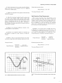
Ftg. 2-2. Measurtng the peak-to-peak voltage of a waveform.
7A18
Operating Instrtictions--7Al8/7A18N
8. Multiply the deflection measured in step 7 by the
VOLTSiDlV switch setting. Include the attenl~ationfactor
of the probe if used.
EXAMPLE: Assume that the peak t o peak vertical deflection is 4.5 divisions (see Fig. 2 - 2 ) using a 10X attenuator probe, and the VO LTSIDIV switch is set to 1 V.
Volts
Peak t o Peak
-
vertical
deflection X 'OL rS'DIV
setting
(divisions)
x
probe
attenuation
factor
Substituting the given values:
Volts Peak-to-Peak= 4.5 X 1 X 10
The peak-to-peak voltage is 45 volts.
Instantaneous Voltage Measurements (DC)
Po measure the DC level at a given point on a waveform,
proceed as follows:
1. Connect the signal to either- input connector.
2 . Set the DISPLAY MODE and TRIGGER SOURCE
switches t o display the channel used.
3 . Set the VOLTSIDIV switch t o display about five
divisions of the waveform.
4. Set the couplinq switch t o GND and pos~tionthe
trace to thc lnottom graticule line or other reference line. If
the voltage i s ncqative with respect t o ground, position the
trace t o the top graticitle line. Do not move the POSl PION
control after this reference line has been establ~shed.
7. Measure the distance in divisions between the
reference line anrf the point on the waveform at which the
DC level i s to be measured. For example, in Fig. 2-3 the
measurement is between the reference line and point A.
8. Establish the polarity of the waveform. With the CH 2
POLARITY switch in the +UP position, any point above
the reference line is ~ositive.
9. Multiply the distance measured in step 7 by the
VOLTS/DIV setting. Include the attentlation factor of the
probe, i f used.
EXAMPLE: Assume the vertical distance measured is 3.6
divisions (see Fig. 2 - 3 ) and the waveform is above the
reference line usinq a 10X probe wit11 a VOLTSIDIV setting
of 0.5 V.
Using the formula:
Instanvertical
VOLTS!
probe
DIV X attenuation
taneous = distance X polarity X
Voltage
(divisions)
setting
factor
Substitllting
given values:
Instantaneous
Voltage
3.6 X
i
1 X 0.5 V X 10
The instantaneous voltage 1s 18 volts.
NOPE
Po n~easrirea voltage Icvel with respect t o a voltage
orher t i ~ a f igrout?d, m a k e the followirig c/)at?ges to
step 4. Set t l ? COLI/?IIII~
~
switch t o DC a r ~ dapply tlte
reference voltage to the inpiit connector. Then
position the trace to the refere17celtne.
5. Set the coupling switch to DC. The ground reference
t o the GND
line can be checked at any time by sw~tclr~nq
position.
6. Set the time-base 'I r~ggeringcontrols for a stable
display. Set the time-base sweep rate for an optinium
display of the waveform.
Fig. 2-3. Measuring instantaneous voltage with respect to some reference.
7A18
Operating Instructions-7Al8/7A18N
Comparison Measurements
I n some applications i t may be desirable to establish
arbitrary units of measurement other than those indicated
by the VOL-ISiDIV switch. This is particularly useful when
comparing unknown signals t o a reference arnpiitcide. One
use for the comparison-measurement technitlue is to
facilitate calibration of equipment where the desired
arnplitude does not produce an exact number of tlivisions
of deflection. The adjustment will be easier and more
accurate if arbitrary units of measurement are established
so that the correct adjiistment is indicated by an exact
number of divisions of deflection. The following procedure
describes how to establish arbitrary units of measure for
conlparison measurcmc?nts.
T o estatrtlish an arbitrary vertical deflection factor- based
upon a specific refert?nccamplitude, proceed as follows:
1. Connect the reference signal to the input connector.
Set the rime-base unit sweep rate t o display several cycles
of tile signal.
Signal
Amplitude
-
VOLT'SIDIV
vertical
vertical
setting
X conversion X deflection
factor
(divisions)
EXAMPLE: Assume a reference signal atnplitude of 30
volts, a VOLTSIDIV setting of 5 V and the VARIABLE
control adjusted t o provide a vertical deflection of four
divisions. Substituting these values in tlie vertical
conversion factor formula (step 4) :
Vertical
Conversion
Factor
3. To estat,lish an arbitrary vertical deflection factor so
the amplitude of an unknown signal can he measured
accurately at any setting of the VOLT-S/DIV switch, the
ai-nl,litude of the t-eierence signal must be icnown. I f i t is
not known, it can be measured before the VARIABLE
VOLTS'DIV control is set in step 2.
4. Divide the atnplitude of the reference signal (volts) by
the product of tho vertical deflection (divisions) established
in step 2 and the settirig of the VOLTS/DIV switch. 1-his is
the vertical conversion factor.
Vertical
Conversion
Factor
reference signal
amplitude
-- -.-- -- - (volts)-vert~cal
VOLTSIDIV
switch
deflection X
(divisions)
setting
30 V
4 X 5 V = 1.5
]-hen with a VOLTS/DIV setting of 2 V, the
peak to-peak amplitude of an unknown signal which
produces a vertical deflection of five divisions can be
determined by using tlie signal amplitut.le formilla (step 6 ) :
Signal
Amnlitude
2. Set tile VOLTS'DIV switch and the VARIABLE
control to produce a display which i s an exact number of
vertical div~sions in atnplitude. Do not cf.tange the
VARIABLE control after obta~nrngthe desiretl cfeflect~on.
-
=
2 V X 1.5 X 5
=
15 volts
Dual-Trace Phase Difference Measurements
Phase conlparison between two signals of the same frequency can be made using the dual-trace feature of the
7A18. 'Th~s method of phase dilference measurement can
be used up to the frequency limit ot the oscilloscope
system. To make the comparison, use the following procedure:
1. Set the CH 1 and CH 2 coi~plingswitches to the same
g
position, clepending on the type of c o t ~ p l i r ~desired.
2. Set the DISPLAY MODE t o A L T or CHOP. I n
general, CHOP is more suitable for low frequencies and
A L T is more suitable for high frequencies. Set the
TRIGGER SOURCE to CH 1.
3. Connect the reference signal to the CH 1 input and
the comparison signal t o the CH 2 input. Use coaxiat cables
or probes which have similar time delay characteristics to
connect the signals to the input connectors.
5. T o measure the amplitude of an unknown signal,
disconnect the reference signal and connect the unknown
signal to the input connector. Set the VOLTSI'DIV switch
to a setting that provides sufficient vertical cleflection to
make an accurate measurement. Do not readjust the
VARIABLE control.
4. I f the signals are of opposite polarity, set the CH 2
POLARITY switch to invert the channel 2 display.
(Signals may be of opposite polarity due to 180' phase
difference; if so, take this into account in t h e final calculation.)
6. Measure the vertical deflection in divisions and
calculate the amplitude of the unknown signal using the
following formula.
5. Set the VOLTS/DIV switches and the VARIABLE
controls of the two channels so the displays are equal and
about five divisions in amplitude.
7A18
Operating Instructions--7A18/7A18N
6. Set the time-base u n i t t o a sweep rate which displays
about one cycle o f t h e waveforms. Set t h e Triggering
controls f o r a stable display.
Substitiitinq the given values:
Phase Difference - 0.3 X 4 5 "
T h e phase difference is 13.5".
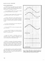
7. Center t h e waveforms o n t h e graticule w i t h t h e 7 A 1 8
POSFTION controls.
High Resolution Phase Measure~nents
8. A d j u s t t h e time-base Variable TitneiDiv c o n t r o l u n t i l
one cycle o f t h e reference signal occupies exactly eight
horizontal divisions between the second and tenth vertical
lines o f the graticule (see Fig. 2-4). Each division o f t h e
graticuie represents 45O of t h e cycle (360° + 8 divisions =
45"idivision). The sweep rate can n o w be stated i n terms o f
degrees as 45'/division.
9. Measure the horizontal difference behveen corresponding points o n t h e waveform.
M o r e accurate dual-trace phase measuremenis can be
made b y increasing the sweep rate ( w i t h o ~ l tchanging the
Variable TirneIDiv c o n t r o l ) . One o f the easiest ways t o increase the sweep rate is w i t h t h e time-base Magnifier switch.
Set t h e Magnifier t o X I 0 and determine the magnified
sweep rate t ~ ydividing the sweep rate obtained previously
b y the amount o f sweep magnification.
E X A M P L E . I f the sweep rate is increased 1 0 times b y
the Magnifier, the magnified sweep rate is 45Oidivision : 10
4.5°/division. Fig. 2 - 5 shows the same signals as used i n
Fig. 2 - 4 b u t w i t h the Magnifier set t o X10. W i t h a i i o r i zontal difference o f 3 divisions, tile phase difference is.
-
10. M u l t i p l y t h e measured distance ( i n divisions) b y
45Oidivision t o obtain t h e exact amount o f phase d i f ference.
E X A M P L E : Assume a horizontal difference o f 0.3 division w i t h a sweep rate of 45°/division as shown i n Fig. 2-4.
S u b s t i t i ~ t i n t the
j given values:
Using the formula:
Phase Difference
horizontal
magnified
sweep rate
Phase Difference - difference X
(divisions)
(cfegreesi'division)
-
hori7ontal
sweep rate
difference X (degrees/division)
(divisions)
Fig. 2-4.Measuring phase difference between two signals.
Phase Difference - 3 X 4.5"
The phase difference is 13.5".
Fig. 2-5.High resolution phase measurement using time-base magriif ier.
2-7
7A18
Operating Instructions--7A18/7A18N
Common Mode Rejection
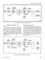
The ADD feature of the 7A18 can be used to display
signals which contain undesirable components. These undesirable components can be eliminated through commonmode rejection. The procedure is as follows:
1 . Set the DISPLAY MODE s~zlitclit o A L T or CHOP
and the TRIGGER SOURCE switch to MODE,
2. Connect the signal containing both the desired and
undesired information t o the CH 1 input connector.
3. Connect a signal similar to the unwanted portion of
tlie CH 1 signal to the CH 2 input connector. For example,
in Fig. 2-6a line-freclcrency signal is connectetl to Channel 2
to cancel out the line-frequency component of the Channel
1 signal.
4. Set botii coupling switches to the same setting, DC or
AC, depericling on the applied signal.
5. Set the VOLTS/DIV switches so the signals are about
equal in amplit~~de.
6. Set tlie DISPLAY MODE switch to ADD. Set the CH
2 POLAR1 r Y switch to INVERT so the common-mode
sign;ils are o f opposite polarity.
7, Adjust the Channel 2 VOLTSiDlV switch and
VAR l ABLE control for maxiinurn cancellation of the
cor~7mon-i~lode
signal. The signal which remains shocrld be
only t l i e desired portion of the Channel 1 signal.
EXAMPLE: An example of this mode of operation is
shown in Fig. 2-6. The signal applied to Charinel 1 contains
unwanted line frequency components (Fig. 2-6A). A corresponding line frequency signal is connected to Channel 2
(Fig. 2-GB). Fig. 2-6C shows the desired portion of tlie
signal as displayed when common-mode rejectioli i s used.
The above procedure can also be used for examining a
signal siiperimposed on some DC level when DC coupling is
usecf. A DC voltage of the Proper polarity
Channel 2 can be used t o cancel out the DC portion of the
signal applied t o Channel 1.
Fig. 2-6.Using the ADD mode for common-mode rejection. ( A )
Channel 3
contains desired information along with linefrequency component. (B) Channel 2 contains line frequency only.
( C f ~ e s t r l t a n tC R T display using common-mode rejection.
7A18
Change information, if any, affecting this section will be found at the rear of this manual.
SOURCE switches. The signal and trigger outputs are
provided t o the oscilloscope via the Interface Connector.
lntroduction
This section of the manual contains a description of the
circuitry used in the 7A18 dual-trace amplifier. The description begins with a discussion of the instrument using the
block diagram shown in the Diagrams section. 'Then, each
circuit is described in detail using block diagrams to show
the interconnections between stages in each major circuit
and the relationship of the front-panel controls to the individual stages.
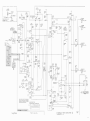
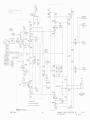
Complete schematics of each circuit are given in the
Diagrams section. Refer t o these schematics throughout the
following circuit description for electrical values and
relationship.
The Readout Encoding circuit (7A18 only) provides
readout logic for the oscilloscope readout system. Data I S
supplied t o the mainframe readout system identifying the
polarity, deflection factor, the uncalibrated symbol (when
the VARIABLE control is in the outward position), and the
plug-in mode. When the IDEN-SIFY button IS pressed, the
trace is deflected about 0.3 division and the deflection
factor readout is replaced by the word "IDEN1-IFY".
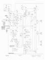
DETAILED CIRCUIT' DESCRIP'TION
ATTENUATOR
General
BLOCK DIAGRAM
The following discussion i s provided to aid in nnderstanding the overall concept of the 7A18 before the individual circuits are discussed in detail. Only the basic interconnections between the individual blocks are shown on
the block diagram (see Diagrams section). Each block
represents a major circuit within the instrument. The
number on each block refers to the schematic on which the
complete circuit i s found.
The Attenuator circuit determines the input coupling
and the 7A18 deflection factor.
NOTE
The Cff I and Cff 2 Attentlator circuits are identicai.
To minimize duplication, only CH 7 is described in
detail throi~ghoutt t ~ i sdiscussion.
AC-GND-DC Switch
The signal t o be displayed on the CRT is applied t o the
input connector. The signal passes through the input
coupling switch, where the appropriate coupling i s selected,
t o the attenuators. The VOLTSIDIV switch selects the
correct amount of attenuation and the signal i s passed to
the input amplifier.
The Channel 1 Input Amplifier circuit provides gain
setting, variable gain control, and trace positioning. The
Channel 2 Input Amplifier provides signal polarity inversion
in addition to gain setting, variable gain control, and trace
positioning. The outputs of these circuits are applied pushpull to the Signal and Trigger Channel Switches.
The Channel Switches select the proper signal and trigger
as determined by the DISPLAY MODE and TRIGGER
Input signals connected to the input connector can be
A C - c o u p l e d , DC-coupled, or internally disconnected.
SlOOA is a cam-type switch; a contact-closure chart
showing the operation i s given on Diagram 1. The dots on
this chart indicate when the associated contacts are III the
position shown (open or closed). When the AC-GND-DC
switch i s in the DC position, the input signal i s cot~pled
directly t o the input Attenuator stage. In the AC position,
the input signal passes through capacitor C10. This capacitor prevents the DC component of the signal from
passing to the amplifier. The GND position opens the signal
path and connects the input circuit of the amplifier to
ground. This provides a ground reference without the need
to disconnect the applied signal from the input connector.
Resistor R 102, connected across the AC-GND-DC switch,
allows C10 t o be precharged in the GND position so the
trace remains on screen when switching to the AC position
if the applied signal has a high DC level.
7A18
Circuit Description--7A18/7Al8N
lnput Attenuator
The ef.fective overall deflection factor of the 7A18 is
determined by the setting o f the VOLTSIDIV switch,
SIOOB. The basic deflection factor i s five millivolts per division of CRT deflection. T o increase the basic deflection
factor t o the values indicated on the front panel, precision
attenuators are switched into the circuit. These attenuators
are hybrid devices which contain the necessary resistances
and capacitors. Each attenuator is replaceahie as a unit.
SIOOB is a cam-type switch and the dots on the contactclosure chart (see Diagram 1) indicate when the associated
contacts are in the position shown (open or closed). I n the
5 mV/Div position, input attenuation i s not used; the input
signal is connected directly t o the input amplifier.
For switch positions above five millivolts, the attenuators are switched into the circuit singly or in pairs t o
produce the deflection factor indicated on the front panel.
These a ttenuators are frequency-compensated voltage
dividers. For DC and low-frequency signals, the attenuators
are primarily resistance dividers and the voltage attenuation
is determined by the resistance ratio i n the circuit. The
reactance of the capacitors in the circuit is so high at low
frequencies that their effect i s negligible. However, at
higher frequencies, the reactance of the capacitors decreases
and the attenuator becomes primarily a capacitance divider.
I n addition to providing constant atLenuation at all
frequencies within the bandwidth of the instrument, the
input attenuators are designed t o maintain the same input
RC characteristics (one megohm X 20 pF) for each setting
of the VOLTS/DIV switch. Each attenuator contains an
adjustable series capacitor t o provide correct attenuation at
high frequencies and an adjustable shunt capacitor t o provide correct input capacitance.
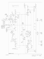
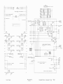
CHANNEL 1
INPUT AMPLIFIER
General
The Channel 1 lnput Amplifier converts the single-ended
signal applied to the Channel 1 input connector to a differential (push-pull) output. Fig. 3-1 shows a detailed block
diagram of the Channel 1 lnput Amplifier. A schematic of
this circuit is shown on Diagram 2 in the Diagrams section.
source for 0210A. 0210A and Q210B are encapsulated in
the same case so that 0210B temperature-compensatesthe
circuit.
Paraphase Cascode Amplifier
Paraphase amplifier 0220-0320, i n conjunction with
0225-0325, forms a cascode amplifier. Q220-Q320 convert
the single-ended input signal t o a differential output signal.
Diodes CR220-CR221 hold the voltage level at the base of
0 2 2 0 close to ground t o limit the voltage swing t o about
40.6 volt. Common-base connected 0225-Q325 provide
isolation between the paraphase amplifier and the GAINVARIABLE controls. 'Phe gain of the Channel 1 lnput
Amplifier is set i n this stage by front-panel GAlN control
R237A with the CAL IN switch pressed in. When the CAL
IN switch is in the outward (uncalibrated) position and
turned fully co~~nterclockwise
to minimum resistance, the
gain o f the amplifier is reduced by a factor of at least 2.5.
Adjustment 1 R321 varies the base level of Q320 t o provide
the same voltage levels at the collectors o f (2225 and 0325.
This prevents a rerouolt reference trace from changing
position when varying the GAlN or VARIABLE controls.
Second Cascode Amplifier
The Second Cascode Amptifier stage provides a signal
gain of approximateiy two. This stage includes the POSITION control and, in the 7A18 only, trace IDENTIFY
circuitry. The emitters of common-base connected
(2250-0350 provide a low-impedance point for injection of
the POSITION control and I D E N r l F Y switch currents.
Position of the trace is determined by the setting of the
POSITION control, R 11. This control changes the current
drive to Q250-0350. Since the emitters are a very lowimpedance point in the circuit, there i s negligible voltage
change at these points. However, the change in current
from the POSI1"ION control produces a resultant DC
voltage difference at the collectors to change the position
o f the trace. Trace identification is accomplished by
inserting resistor R357 from ground through CR357 t o the
junction of R11-R256. This results in a slight increase in
the emitter current of Q250 t o cause the trace t o move.
This aids in identifying the channel 1 trace when multiple
traces are displayed.
The network C246-C345-C245-R246-R345-R245 provides high frequency compensation. R245-C245 in this network provide high-frequency response adjustment for this
stage.
lnput Source Follower
The Input Source Follower Q210A provides a high input
impedance with a low impedance drive for the following
stage. R210 limits the current drive to the gate of Q210A.
Dual-diode CR210 provides circuit protection by limiting
the voltage swing at the gate of 0210A to about 4 (positive
or negative) 15 volts. Q210B provides a constant current
Emitter Follower
Emitter Follower stage 0260-(2360 provides a low output impedance t o drive the Signal and Trigger Channel
Switches, U270-U470. This stage also provides isolation
between the Second Cascode Amplifier and U270-U470.
7A18
Circuit Description-7Al8/7A18N
CHANNEL SWITCH
-
+
U470
Fig. 3-1. Channel 1 lnput Amplifier detailed block diagram.
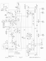
CHANNEL 2 INPOUAMPLIFIER
General
The Channel 2 lnput Amplifier circuit is basically the
same as the Channel 1 lnput Amplifier circuit. Only the
differences between the two circuits are described here.
Portions of this circuit not described in the following description operate in the same manner as for the Channel 1
lnput Amplifier circuit (corresponding circuit numbers
assigned in the 400 599 range). Fig. 3-2 shows a detailed
block diagram of the Channel 2 lnput Amplifier circuit. A
schematic of this circuit i s shown on Diagram 3 in the
Diagrams section.
Paraphase Cascode Amplifier
The Paraphase Cascode Amplifier for Channel 2 consists
of Q420, Q520, (3425, Q525,0426, and Q526. In addition
to the functions described under Channel 1 lnput Amplifier, the Channel 2 Paraphase Cascode Amplifier stage
provides a means of inverting the displayed signal. With the
CH 2 POLARI1-Y switch set to +UP, 0425 and 0525 are
biased on and the signal i s passed to the Second Cascode
Amplifier stage as for the Channel 1 lnput Amplifier. With
the CH 2 POLARITY switch set t o INVERT, Q425 and
Q525 are biased off and Q426-Q526 are turned on to
provide signal inversion.
PARAPHASE
TO
SIGNAL
GMANNEL
SWITCH
U270
FROM
INPUT
ATTEN
CHANNEL
FROM
SWiTCW
U470
S23
17A18 ontv)
Fig. 3-2.Channel 2 lnput Amplifier detailed block diagram.
REV. D, DEC. 1976
7A18
Circuit Description-7Al8/7A18N
Second Cascode Amplifier
Ttie Second Cascode Amplifier for Channel 2 consists of
0440, 0540, Q450, and Q550. Position of the trace i s set
by the POSITION control, R21 or by network R455-H555
as determined by the DISPLAY MODE switch. I n any DISPLAY MODE switch position other than ADD, i 50 volts i s
applied t o the center arm of the POSl I^ION control through
R32. The POSITION control varies the current drive t o the
emitters of Q450-0550. Since the emitters are a very lowimpedance point in the circuit, there is negligible voltage
change at these points. However, the change in current
from the POSITION control produces a resultant DC
voltagt-: difference at the collectors to change the position
of the trace. When the DISPLAY MODE switch is in the
ADD position, +50 volts i s applied to the junction of resistors R455-R555 through R32 t o balance the current drive
t o the emitters of (2450-0550. This results in a fixed zero
volts (approximately) difference between the collectors.
Since +50 volts is not applied to the POSII-ION control in
the ADD position of the DISPLAY MODE switch, the
control setting has no effect on the circuit operation.
CHANNEL SWITCHES
General
Ttie Channel Switches circuit provides Signal and Trigger
outputs to the oscilloscope via the Interface Connector as
determined by the DISPLAY MODE and THIC<GER
SOURCE switches. A schematic of this circuit is given on
Diagram 4 i n the Diagrams section.
Signal Channel Switch
The Signal Channel Switch stage consists of integrated
circuit U270 and its external components. This staqe selects
one, or mixes two input analog signals in response t o inputs
from tlie DISPLAY MODE switch. The Signal Cliannel
Switch stage determines which input (CH 1 or CH 2) provides the signal t o the oscilloscope as controlled by the
DISPLAY MODE switch setting. Resistors R276-R277 and
R376-R377 set the current gain for each channel. Networks
C274-R274-C215-R275 and C374-R374-C375-R375 provide high-frequency compensation for each channel. C275
and C315 in these networks are high-frequency compen.
sation adjustments.
DISPLAY M O D E
SELECTED
m
m
---
*Level is switched between the HI-level and LO-level a t an approximate 0.5 megahertz rate.
I
I
**Level is switched between the Hl-level and LO-level at a rate
determined by the setting of the time-base unit sweep rate.
Fig. 3-3. U270 input combinaliotis for DISPLAY M O D E selection
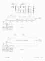
'Trigger Channel Switching
The Trigger Channel Switch U470 i s identical t o the
Signal Channel Switch. This stage determines which input
(CH 1 or CH 2) provides the trigger stgnal for internal
triggering of the time-base unit. 7 he selection of the trigger
signal is controlled by inputs from the TRIGGER SOURCE
switch. Resistors R476-R477 and R576-R577 set the curr e n t g a i n f o r each channel. Networks
C474-R474-C475-R475 and C574-R574-C575-R575 provide high-frequency compensation for each channel.
A n inputloutput table for this stage is shown in Fig. 3-4.
Wlien the level at pin 14 is LO, the output of U470 is
determined by the level at pin 4. With the level at pin 14 HI
and the level at pin 4 LO, the channel 1 and channel 2
triggers are added algebraically.
Signal and
Output
'Phe Signal Output stage, Q280-Q380, and the Trigger
Output stage, 0480-0580, are similar. Each stage consists
of a pair of common-base connected transistors which provide the DC level shifting necessary to drive the mainframe
circuits.
DISPLAY MODE A N D
Fig. 3-3 shows the U270 input combinations for each
position of the DISPLAY MODE switch. When the level at
pin 14 is LO the output of U270 is determined by the level
at pin 4. With the level at pin 14 H I and the level at pin 4
LO, the signals from both channel 1 and channel 2 are
passed to the Signal Output stage. This condition occurs
only when the DISPLAY MODE switch is set t o ADD. In
this operating mode the signal output i s the algebraic sum
of channel 1 and channel 2 signals and the resultant signal
determines the mainframe deflection.
TRIGGER SWI"T'CHING
General
The Display Mode and Trigger Switching circuit determines which input signal (Channel 1 or Channel 2) providcs
the Signal and Trigger outputs to the mainframe as selected
by the DISPLAY MODE and TRIGGER SOURCE switches.
This circuit also provides plug-in mode information t o the
mainframe chop blanking circuit, and readout control information for proper CRT display.
7A18
Circuit Description--7A18/7A18N
Readout Encoding (7A18 only)
DISPLAY M O D E Switch
'The DISPLAY MODE switch provides logic level outputs
to the Signal Channel Switch stage (U270, Channel
Switches diagram 4). A table of the outputs for each
position of the DISPLAY MODE switch is shown in Fig.
3-3.
'TRIGGER SOURCE Switch
The TRIGGER SOURCE switch provides logic level outputs t o the Trigger Channel Switch (U470, Channel
Switches diagram 4). A table of the outputs for each switch
position is shown in Fig. 3-4.
'The Readout Encoding circuit consists of switching
resistors and probe sensing stage Q620. This circuit encodes
the Channel 1 and 2, Row and Column output lines for
readout of deflection factor, uncalibrated deflection factor
(VARIABLE) information, and signal inversion (channel 2
only). Data is encoded on these output lines by switching
resistors between them and the time-slot input lines, or by
adding current through 0620.
R647-CR647 are switched between time-slot three
(TS-3) and Column output line when the CAL IN switch is
(greater
in the uncal position. This results in the symbol
than) being displayed preceding the deflection factor readout. R648 (Channel 2 only) is switched between TS-2 and
the Column output line when the CH 2 POLARITY switch
is in the INVERT position. This results in the symbol 1
(inverted) being displayed preceding the deflection factor
readout.
>
Trigger S~gnaI
Source
--"--------- ------ ---
I
ALT
1-G6-D-E
.f-"T--i5
*f-.
-cG"-t""Ei
;-me..--
--*
----- -
ernates between GW 1
and
CH 2
+-*
.--*-
-"------
-
---cw_
?.----"---GM 1 and CW 2 added
CY"?-..
-"-----"
Switching resistors are used to indicate the setting of the
VOLTSiDIV switch to the mainframe readout system. The
VOLTSIDIV switch is a cam-type switch. The dots on the
contact-closure chart (see Diagram 6) indicate when the
associated contacts are closed. R633, R634, and R635
select the number 1, 2, or 5 depending on the resistor
combination that i s switched in. R637 selects the m (milli-)
prefix and R639 selects the symbol V (volts) in the 5 mV
through .5 V (500 m V ) positions of the VOLTSiDIV
switch. R638 selects the symbol V in the 1, 2, and 5 V
positions. R630, R631, and the output of the probe sensing
stage (0620) select the decimal point (number of zeroes)
again depending on the resistor combination switched in by
the VOLTSiDIV switch.
Fig. 3-4. Input/Output combinations for DISPLAY MODE and
'TRIGGER SOURCE switch selections.
CONNECTORS A N D READOUT
General
The Connectors and Readout circuit consists of the
power supply and signal distribution from the lnterface
Connector and the Readout Encoding circuit. A schematic
of this circuit i s shown on Diagram 6 in the Diagrams
section.
Connectors
All the connections made to the mainframe by the 7A18
are shown on the Connectors portion of Diagram 6. Also
shown are the power sopply decoupling components.
Probe sensing stage Q620 identifies the attenuation
factor of the probe connected t o the input connector by
sensing the amount of current flowing from the current
sink through the probe coding resistance. The output of
this circuit corrects the mainframe readout system to include the probe attenuation factor. 'The third contact of the
input connector provides the input t o the probe sensing
stage from the probe coding resistance (coded probes
only; see 0pera;ing Instructions). The third contact is also
used for the IDENTIF-Y input. The coding resistor forms a
voltage divider with R621 through CR621 to the - - I 5 V
supply. The resultant voltage sets the bias on Q620 and
determines, along with emitter resistor R622, the collector
current. When the -15 volt time-slot pulse is applied to
Interface Connector B33, 0 6 2 0 is interrogated and i t s
collector current i s added to the column current output
through Interface Connector A37.
REV. D, JAN. 1975
7A18
Circuit Description--7A1817A18N
With a 1X probe (or no probe) connected t o the input
connector, 0 6 2 0 is turned off. The deflection factor readout i s determined by the VOLTS!DIV switch position. With
a 10X probe connected, the bias on 0 6 2 0 will allow 100
microamperes of collector current to flow. 1-his increases
the deflection factor readout by a factor of 10.
The IDENTIFY button (S13 or 523 on Diagram I ) does
two things when pressed :
I.It causes the trace representing the appropriate
channel of the 7A18 to move about 0.3 division (see the
discussion on the Channel 1 or Channel 2 Input Amplifier).
2. Forward biases CR621 and Q620 t o result in a
sufficient amount of collector current which, when added
t o the column current output, replaces the deflection factor
readout with the word "IDENTIFY".
These two actions aid in identifying the 7A18 trace
when multiple traces are displayed. When the IDENTIFY
button i s released, the deflection factor readout and trace
position are restored.
For further information on the operation of the readout
system, see the oscilloscope instruction manual.
7A18
Change information, i f any, affecting this section will be found at the rear of this manual.
lntroduction
Lubrication
This section of the manual contains maintenance information for use in preventive maintenance, corrective maintenance, and troubleshooting of the 7A18.
Use a cleaning-type lubricant on shaft bushings, interconnecting plug contacts, and switch contacts. Lubricate
switch detents with a heavier grease. A lubrication kit
containing the necessary lubricating materials and instructions is available through any Tektronix Field Office. Order
Tektronix Part Number 003-0342-01.
Further maintenance information relating to component
color codes and soldering techniques can be found in the
instruction manuals for the 7000-series oscilioscopes.
PREVEN'TIVE MAINTENANCE
Recalibration
To ensure accurate measurements, the 7A18 should be
checked after each 1000 hours of operation or every six
months if used infrequently. A complete performance
check procedure i s given in Part I for Section 5.
General
Preventive maintenance, consisting of cleaning, visual
inspection, lubrication, etc., performed on a regular basis,
will improve the reliability of this instrument. Periodic
checks on the semiconductor devices used in the unit are
not recommended as a preventive maintenance measure.
See semiconductor-checking information given under
Troubleshooting.
The performance check procedure can be helpful in
isolating major troubles in the unit. Moreover, minor
troubles not apparent during regular operation may be
revealed and corrected.
TROUBLESHOOTING
Cleaning
Avoid the use of chemical cleaning agents which
might damage the plastics in this instrument. Avoid
chemicals containing benzene, toluene, xylene, acetone, or similar solvents.
Front Panel. Loose dust may be removed with a soft
cloth or a dry brush. Water and mild detergent may be
used; however, abrasive cleaners should not be used.
Interior. Cleaning the interior of the unit should precede calibration, since the cleaning process could alter the
settings of the calibration adjustments. Use low-velocity
compressed air to blow off the accumulated dust. Hardened
dirt can be removed with a soft, dry brush, cotton-tipped
swab, or cloth dampened with a mild detergent and water
solution.
General
The following i s provided to augment information
contained in other sections of this manual when troubleshooting the 7A 18. The schematic diagrams, Circuit
Description, and Calibration sections should be used to full
advantage. The Circuit Description section gives detailed
information on circuit behavior and output requirements.
Troubleshooting Aids
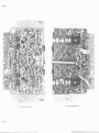
Diagrams. Circuit diagrams are given on foldout pages in
Section 7. The circuit number and electrical value of each
component in this instrument are shown on the diagrams.
important voltages are also shown.
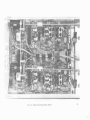
Circuit Board. The circuit board used in the 7A18 is
outlined on the schematic diagrams, and a photograph of
the board i s shown on the back of Diagram 1. Each
board-mounted electrical component is identified on the
photograph by i t s circuit number.
7A18
Component and Wiring Color Code. Colored stripes or
dots on resistors and capacitors signify electrical values,
tolerances, etc., according to the EIA standard color code.
Components not color coded usually have the value printed
on the body.
2 . DC Voltmeter and Ohmmeter -A voltmeter for
checking voltages within the circuit and an ohmmeter for
checking resistors and diodes are required.
3. Test Oscilloscope-.A test oscilloscope is required to
view waveforms at different points in the circuit.
The insulated wires used for interconnection in the
7A18 are color coded to facilitate tracing a wire from one
point to another in the unit.
Semiconductor Lead Configuration. Fig. 4-1 shows the
lead configuration of the semiconductor devices used in this
instrument.
A Tektronix 7000-series Oscilloscope equipped with a
readout system, 7D13 Digital Multimeter unit, 76-series
Time-Base unit, and a 7A-series Amplifier unit with a 10X
probe will meet the needs for items 2 and 3.
Troubleshooting Procedure
Troubleshooting Equipment
The following equipment is useful for troubleshooting
the 7A 18.
1. Semiconductor Tester--Some means of testing the
transistors, diodes, and FET's used in this instrument is
helpful. A transistor-curve tracer such as the Tektronix
Type 576 will give the most complete information.
This troubleshooting procedure is arranged in an order
which checks the simple trouble possibilities before proceeding with extensive troubleshooting.
1. Check Control Setting. A n incorrect selting of the
7A18 controls can indicate a trouble that does not exist. I f
there is any question about the correct function or operation of a control or front-panel connector, see the
Operating Instructions section.
Fig. 4-1. Electrode configuration for semiconductors used in this instrument.
7A18
2. Check Associated Equipment. Before proceeding
with troubleshooting o f the 7A18, check that the equipment used w i t h this instrument is operating correctly. I f
possible, substitute an amplifier u n i t known t o be operating
correctly into the indicator u n i t and see i f the problem
persists. Check that the inputs are properly connected and
that the interconnecting cables are n o t defective.
3. Visual Check. Visually check the portion of the
instrument i n which the trouble is suspected. Many troubles
can be located b y visual indications, such as unsoldered
c o n n e c t i o n s , broken wires, damaged circuit boards,
damaged components, etc.
4. Check Instrument Performance. Check the calibration o f the unit, or the affected circuit b y performing
Part I -- Performance Check o f Section 5. The apparent
trouble may only be a result o f misadjusrment and may be
corrected b y calibration. Complete calibration instructions
are given i n Part II o f Section 5.
5. Check Voltages and Waveforms. Often the defective
component o r stage can be located b y checking f o r the
correct voltage or waveform i n the circuit. Typical voltages
and waveforms are given o n the diagrams; however, these
are n o t absolute and may vary slightly between instruments. T o obtain operating conditions similar t o those used
t o take these readings, see the instructions i n the Diagrams
section.
6. C h e c k l n d i v idual Components. The following
methods are provided f o r checking the individual components i n the 7A18. Components which are soldered in place
are best checked b y disconnecting one end t o isolate the
measurement from the effects o f surrounding circuitry.
A. 'TRANSISTORS A N D INTEGRATED CIRCUITS.
T h e best check o f transistor and integrated circuit
operation is actual performance under operating conditions.
I f a transistor or integrated circuit is suspected of being
defective, it can best be checked by substituting a component known t o be good; however, be sure that circuit
conditions are n o t sl.ich that a replacement might also be
damaged. I f substitute transistors are n o t available, use a
dynamic tester (such as Tektronix Type 576). Static-type
testers may be used, b u t since they d o n o t check operation
under simulated operating conditions some defects may go
unnoticed. Fig. 4-1 shows base p i n and socket arrangements
o f semiconductor devices. Be sure the power is o f f before
attempting t o remove or replace any transistor or integrated
circuit.
Integrated circuits can be checked w i t h a voltmeter, test
oscilloscope, or b y direct substitution. A good understanding of the circuit description is essential t o troubleshooting circuits using integrated circuits. Use care when
checking voltages and waveforms around the integrated
circuits so that adjacent leads are n o t shorted together. A n
integrated-circuit test clip provides a convenient rneans of
clipping a test probe t o the 14- and 16-pin integrated circuits. Phis device also doubles as an integrated-circuit
extraction tool.
B. DIODES. A diode can be checked f o r an open or for
a short circuit b y measuring the resistance between terminals with an ohmmeter set t o the R X Ik scale. The diode
resistance should be very high i n one direction and very low
when the meter leads are reversed. D o n o t check tunnel
diodes or back diodes with an ohmmeter.
Do not use an ohmmeter scale that has a high internal
current. High currents may damage the diodes.
C. RESISTORS. Check resistors w i t h an ohmmeter.
Resistor tolerance is given i n the Electrical Parts List.
Resistors normally d o n o t need t o be replaced unless the
measured value varies widely from the specified value.
D. CAPACITORS. A leaky or shorted capacitor can be
detected b y checking resistance with an ohmmeter o n the
highest scale. Use an ohmmeter which will n o t exceed the
voltage rating o f the capacitor. The resistance reading
should be high after initial charge o f the capacitor. A n open
capacitor can best be detected with a capacitance meter, or
by checking whether the capacitor passes AC signals.
7. Repair and Readjust the Circuit. Special techniques
required t o replace components i n this u n i t are given under
Component Replacement. Be sure t o check the performance o f any circuit that has been repaired o r that has had
any electrical components replaced. Recalibration o f the
affected circuit may be necessary.
REPLACEMEN-T PARTS
Standard Parts
A i l electrical and mechanical part replacements for the
7A18 can be obtained through your local Tektronix Field
Office or representative. However, many o f the standard
electronic components can be obtained locally i n less time
than is required t o order them from Tektronix, Inc. Before
purchasing o r ordering replacement parts, check the parts
lists f o r value, tolerance, rating, and description.
REV. D, MAY, 1975
7A18
COMPONENT REPLACEMENT
When selecting replacement parts, i t is important to
remember that the physical size and shape o f the
component may affect its performance in the instrument. All replacement parts should be direct replacements unless i t is known that a different component
will not adversely affect the instrument performance.
General
The exploded-view drawing associated with the Mechanical Parts List may be helpful when disassembling or reassembling individual components or sub-assemblies.
Circuit Board Removal
Special Parts
Some parts are manufactured or selected by Tektronix
t o satisfy particular requirements, or are manufactured for
Tektronix t o our specifications. These special parts are
indicated in the parts list by an asterisk preceding the part
number. Most of the mechanical parts used in this instrument have been manufactured by Tektronix. Order all
special parts directly from your local Tektronix Field
Office or representative.
I n general, the circuit boards used in the 7A18 need
never be removed unless they must be replaced. Electrical
connections t o the boards are made by soldered connections. I f it i s necessary t o replace a circuit board
assembly, use the following procedures.
A. READOUT CIRCUIT BOARD REMOVAL (7A18 only)
1. Disconnect the wires connected t o the outside of the
board.
Ordering Parts
When ordering replacement parts from Tektronix, Inc.,
refer to the Parts Ordering Information and Special Notes
and Symbols on the page immediately preceding the Electrical Parts List section. Include the following information:
1. lnstrument type (7A18)
2. Instrument Serial Number
3. A description of the part (if electrical, include the
circuit number)
4. Tektronix Part Number
Soldering Techniques
Attenuator Circuit Boards. The Attenuator circuit
boards are made from polyphenylene oxide because of i t s
excellent electrical characteristics. Use more than normal
care when cleaning or soldering this material. The following
rules should be observed when removing or replacing parts:
2. Remove the seven screws holding the board t o the
mounting surface.
3. Disconnect the wires connected to the inside of the
board.
4. Remove the board from the unit.
5. To replace the board, reverse the order of removal.
B. ATTENUATOR CIRCUIT BOARD REMOVAL
1. Remove the readout board as outlined in the previous
procedure.
2. Disconnect the resistor/capacitor connected t o the
rear of the board.
3. Loosen the front set screw on the VARIABLEIGAIN
control shaft coupling (use a 0.050-inch hex-key wrench).
1. Use a very small soldering iron (not over 15 watts)
4. Retnove the red VARIABLE control knob and rod
from the control shaft.
2. Do not apply more heat, or apply heat for a longer
time, than is absolutely necessary.
5. Remove the remaining front-panel knobs using a
1116-inch hex-key wrench.
3. Use a vacuum-type desoldering tool t o remove the
excess solder from the circuit board.
6. Remove the front panel from the instrument.
7. Remove the attenuator shields.
4. Do not apply any solvent containing ketones, esters,
or halogenated hydrocarbons.
5. To clean, use only water-soluble detergents, ethyl,
methyl, or isopropyl alcohol.
8. Disconnect the wires and resistor from the input BNC
connector.
9. Remove the input BNC connector.
7A18
10. Remove the POSITION control using a 5116-inch
nut driver.
11. Remove the attenuator board with cam switch from
the instrument.
12. To replace the board, reverse the order o f removal.
B. ROTARY SWITCHES
Single wafers on the DISPLAY MODE and TRIGGER
SOURCE switches are not normally replaced. I f any part of
these switches i s defective, the entire switch assembly
should be replaced. A new switch can be ordered through
your Tektronix Field Office.
C. AMPLIFIER CIRCUIT BOARD REMOVAL
1. Remove the Readout circuit boards as given previously.
2. Remove the plastic plug-in guide from the rear of the
instrument.
3. Disconnect the wires connected t o the board from
the front-panel controls.
4. Loosen the front hex-socket screw in the front
c o u p l i n g o f the VARIABLE control shaft using a
0.050-inch hex-key wrench. Pull the VARIABLE knob and
shaft from the front of the instrument.
5. Loosen the front hex-socket screw in the coupling
between the DISPLAY MODE and 'TRIGGER SOUCE
switch sections. Pull the T'RIGGER SOURCE knob and
long shaft from the front of the instrument.
6. Loosen the front hex-socket screw in the coupling of
the DISPLAY MODE switch shaft using a 5116-inch hexkey wrench. Pull the DISPLAY MODE knob and long shaft
from the front of the instrument.
7. D i scon n e c t the resistor-capacitor combinations
connected t o the ceramic strips at the front of the board.
8. Remove the screws and nuts securing the board t o
the chassis or other mounting surface.
When disconnecting or connecting leads to a wafertype rotary switch, do not let solder flow around and
beyond the rivet on the switch terminal. Excessive
solder can destroy the spring tension of the contact.
Transistor and Integrated Circuit Replacement
Transistors and IC's should not be replaced unless
they are actually defective. I f removed from their sockets
during routine maintenance, return them to their original
sockets. Special care must be given to integrated circuit
leads, because they can easily be damaged in removal
from sockets. Unnecessary replacement or switching of
components may affect the calibration of the instrument.
When a transistor i s replaced, check the operation of that
part of the instrument that may be affected.
Recalibration After Repair
After any electrical component has been replaced, the
calibration of that particular circuit should be checked, as
well as the calibration of other closely related circuits. The
Performance Check instructions given in Part I of Section 5
provide a quick and convenient means of checking the
instrument operation. The Calibration Procedure in Part I I
of Section 5 can then be used t o adjust the operation to
meet the Performance Requirements listed in Section 1.
9. Remove the board from the instrument.
Repackaging for Shipment
10. T o replace, reverse the order of removal.
If the 1-ektronix instrument is to be shipped to a 1-ektronix
Service Center for service or repair, attach a tag showing:
owner (with address) and the name of an individual a t your
firm that can be contacted, complete instrument serial
number and a description of the service required.
Switch Replacement
Several types o f switches are used in the 7A18. The
following special maintenance information is provided for
the cam-type switches and rotary switches.
A. CAM-TYPE SWITCHES
m
CAUTION
Repair o f cam-type switches should be undertaken
only by experienced maintenance personnel. Switch
alignment and spring tension of the contacts must be
carefully maintained for proper operation o f the
switch. For assistance in maintenance o f the cam-type
switches, contact your local Tektronix Field Office or
represen ta tive.
REV. E DEC 1976
Save and re-use the package in which your instrument was
shipped. If the original packaging i s unfit for use or not
available, repackage the instrument as follows:
Surround the instrument with polyethylene sheeting t o
protect the finish of the instrument. Obtain a caiton of
corrugated cardboard of the correct carton strength and
having inside dimensions of no less than six inches more
than the instrument dimensions. Cushion the instrument
by tightly packing three inches of dunnage or urethane
foam between carton and instrument, on all sides. Seal
carton with shipping tape or industrial stapler
The carton t e s t strength for your instrument is 200 pounds.
4-5
7A18
Change information, i f any, affecting this sec,tion will be found at the rear o f the manual.
Recalibration l nterval
To assure instrument accuracy, check the calibration of
the 7A18 every 1000 hours of operation, or every six
months if used infrequently. Before complete calibration,
thoroughly clean and inspect this instrument as outlined in
the Maintenance section.
Tektronix Field Service
Tektronix, Inc. provides complete instrument repair and
recalibration at local Field Service Centers and the Factory
Service Center. Contact your local Tektronix Field Office
or representative for further information.
instrument is both correctly adjusted and performing
within all Performance Requirements as given in Section 1.
TEST' EQUIPMEN'T REQUIRED
General
The following test equipment and accessories, or its
equivalent, is required for complete calibration of the
7A18. Specifications given for the test equipment are the
minimum necessary for accurate calibration. Therefore,
some of the specifications listed here may be somewhat less
precise than the actual performance capabilities of the test
equipment. All test equipment is assumed t o be correctly
calibrated and operating within the listed specifications.
Using 'This Procedure
General. This section provides several features to facili
tate checking or adjusting the 7A18. These are:
Index. T o aid in locating a step in the Performance
Check or Adjustment procedure, an index is given preceding Part I ---- Performance Check and Part I I -- Adjustment procedure.
Performance Check. The performance of this instrument can be checked without removing the side shields or
making internal adjustments by performing only Part I
Performance Check. This procedure checks the instrument
against the tolerances listed in the Performance Requirement
column of Section 1. I n addition, a cross-reference is provided to the step in Part I I --- Adjustment which will return
the instrument to correct calibration. In most cases, the
adjustment step can be performed without changing control
settings or equipment connections.
Adjustment Procedure. To return this instrument t o
correct calibration with the minimum number of steps,
perform only Part I I - - Adjustment. The Adjustment procedure gives the recommended calibration procedure for all
circuits in this instrument.
Complete Performance Check/Adjustment. T o completely check and adjust all parts of this instrument, perform both Parts I and I I. Start the complete procedure by
performing the Adjustment procedure and follow this with
the Performance Check. 'i'his method will assure that the
The Performance Check and Adjustment procedures are
based on this recommended equipment. I f other equipment
is substituted, control settings or calibration setup may
need t o be altered to meet tlie requirements of the equipment used. Detailed operating instructions for the test
equipment are not given in this procedure. Refer to the
instruction manual for the test equipment if more information is needed.
Calibration Equipment Alternatives
All of the test equipment is required to completely
check and adjust this instrument. However, some of the
items used only for the Performance Check can be deleted
w i t h o u t compromising the instrument's measurement
capabilities. For example, the low-frequency constantamplitude signal generator is used on1y in the Performance
Check and may be deleted if the user does not desire to
check the lower frequency response or triggel- source
operation. Equipment used only for the Performance
Check procedure is indicated by note 1; items required
only for tlie Adjustment procedure are indicated by
note 2.
Test Equipment
1. 7000-series oscilloscope, referred to as the Indicator
Oscilloscope in this procedure. Tektronix 7403 recommended.
2. T'ime-Base plug-in unit, Tektronix 7B50.
7A18
3. Amplitude Calibrator. Output signal, one kilohertz
square wave; output amplitude, 20 millivolts to 20 volts;
amplitude accuracy, within 0.25%. Vektronix PG 506
Pulse Generator re~ommended.~
4. Medium-frequency constant-amplitude sine-wave generator.' Frequency, variable from 50 to 75 megahertz;
reference frequency, 50 kilohertz; output amplitude, variable from 50 millivolts to 200 millivolts into 50 ohms;
amplitude accuracy, output amplitude constant within 3%
at 50 kilohertz and from 50 to 75 megahertz. For example,
Tektronix SG 503 Signal en era tor.^
5. Low-frequency constant-amplimde signal generator.'
Frequency range, two hertz to 10 kilohertz; output amplitude, variable from 10 millivolts to 400 millivolts peak to
peak. For example, General Radio 1310-B Oscillator (use
General Radio Type 274 ClBJ Adapter to provide BNC output).
Must have the following out6. Square-wave
put capabilities (may be obtained from separate generators): 12 volts amplitude into 50 ohms at one kilohertz
with a risetime of 12 nanoseconds or less; 500 millivolts
into 50 ohms at 100 kilohertz with a risetime of one nanosecond or less. Tektronix PG 506 Pulse Generator recommended (meets both output requirements).3
7. Plug-in extender.'
0589-00.
Tektronix Part Number 067-
14. In-line BNC termination.' Impedance, 50 ohms;
wattage rating, two watts; accuracy, 22%; connectors,
BNC, Tektronix Part No. 01 1-0049-01.
15. 10X BNC attenuator.' Impedance, 50 ohms; accuracy, +2%; connectors, BNC. Tektronix Part No.
0 11-0059-02.
16. Input RC normalizer.' Time constant, one megohm
X 20 picofarads; attenuation, 2X; connectors, BNC. Tektronix calibration fixture 067-0538-00,
17. ~ d a ~ t e r .Adapts
'
GR874 connector to BNC male
connector. Tektronix Part No. 017-0064-00.
Adjustment Tools
18. Screwdriver. Three-inch shaft, 3132-inch bit. For
example, Xcelite R-3323.
19. Low-capacitance s~rewdriver.~1 1/2-inch shaft.
Tektronix Part No. 003-000@00.
20. Tuning tool.2 Handle with inserts for input capacitance and attenuator adjustments. 'T'ektronix Part No.
003-0307-00,003-0334-00, and 003-0497-00.
Accessories
Preliminary Control Settings
8. l&inch cable.' Impedance, 50 ohms; type, RG-58/U;
connectors, BNC. Vektronix Part No. 012-0076-00.
Set the Indicator Oscilloscope and 7A18 controls as
follows (for both Performance Check and Adjustment
procedure):
9. 42-inch cable. Impedance, 50 ohms; type RG-581U;
connectors, BNC. Tektronix Part No. 012-0057-01.
10. Five-nanosecond cable. Impedance, 50 ohms; type,
R G-2 13/U; connectors, GR874. Tektronix Part No.
017-0502-00.
1 1. In-line G R termination. Impedance, 50 ohms; wattage rating, two watts; accuracy, f 2%; connectors, GR874
i n p u t w i t h BNC male output. Tektronix Part No.
017-0064-00.
12. Dual-input coupler.' Matched signal transfer to each
input. Tektronix calibration fixture 067-0525-00.
13. 10X GR a t t e n ~ a t o r . ~Impedance, 50 ohms;
accuracy, +2%; connectors, GR874. Tektronix Part No.
017-0078-00.
' Required only for Psrforlnance Check.
Required only for Adjustment procedure.
Requires TM 500-Series Power Module.
lndicator Oscilloscope
l ntensity
Focus
Mid range
Adjust for well-defined
display
As desired
40 mV
I kHz
Left
Left Vert
Graticule lllum
Calibrator
Rate
Vert Mode
Trig Source
7A18
DISPLAY MODE
TRIGGER SOURCE
CH 2 POLARITY
CH 1
MODE
+UP
CH 1 and CH 2
POSlrlON
VO LTSlD IV
AC-GND-DC
Midrange
10 mV
DC
REV.
E, MAY, 1976
7A18
Performance Check-7A1817A18N
P A R T I - P E R F O R M A M C E CHECK
Introduction
The following procedure checks the performance of the
7A18 without removing the covers or making internal
adjustments. All tolerances given in this procedure are
based on Section 1 of this manual.
Index to Part I
-- Performance Check
2. Connect the Indicator Oscilloscope to a power source
which meets the frequency and voltage requirements of the
power supply.
3. Turn the indicator Oscilloscope power on. Allow at
least twenty minutes warmup for checking the 7A18 to the
given accuracy.
Page 5-3
1. Check Channel 1 and 2 GAIN
2. Check Channel 1 and 2 Deflection
Factor Accuracy
Page 5-3
3. Check Channel 7 and 2 VARIABLE
(VOLIS/DIV) Range
Page 5-4
4. Check Channel 1
IDENTIFY (7A18 only)
'Trace
Page 5-4
5. Check Channel 1 and 2 Upper Bandwidth
Page 5-4
6. Check Channel 1 and 2 Lower Frequency Response
Page 5-4
4. Set the controls as given under Preliminary Control
Settings.
NOTE
and
2
The checks titled Channel I and 2 apply equally to
both channels. Perform the check on the channel
selected by the DISPLA Y MODE switch.
1. Check Channel I and 2 GAIN
7. Check Channel Isolation
Page 5-5
8. Check Common-Mode Rejection Ratio
Page 5-5
9. Check Alternate Operation
Page5-5
10. Check Chopped Operation
Page 5-6
11. Check Trigger Source Operation
Page5-6
a. Connect the standard amplitude calibrator output to
the CH 1 and CH 2 input connectors with the 42-inch BNC
cable and dual-input coupler.
b. Set the standard amplitude calibrator for a 50millivolt square-wave otltpu t.
c. CHECK--CRT display for a five-division display.
d. I f necessary, adjust the front-panel GAlN control for
exactly five divisions of vertical deflection. T o adjust, press
in the GAlN knob with a screuldriver and turn until the
GAlN control is engaged.
e. Set the DISPLAY MODE switch to CH 2 and repeat
parts c and d of this step for Channel 2.
Preliminary Procedure for Performance Check
NOTE
The perforn~anceo f this insrnrmenf can be checkecl
at any temperature within the 0°C to +50°c range
unless stated otherwise.
1 . Instail the 7 A ? 8 i n the left vertical plug-in cornpartrnent of the Indicator Oscilloscope.
2. Check Channel 1 and 2 Deflection Factor
Accuracy
a. Set the Channel 1 AC-GND-DC switch to GND.
b. CHECK-Using the VOLIS/DlV and standard amplitude calibrator settings given in Table 5-1, check vertical
deflection within 2% in each position of the VOLTS/DIV
switch.
7A18
Performance Check--7A1817A18N
c, Change the following conttal settings.
DISPLAY MODE
CH 1 AC-GRID-DC
CH 2 AC-GND-DC
CH 1
DC
GND
ti Repeat part b of this step for Channel I
TABLE 5-1
4. Check Channel 1 and 2 Trace IDENTIFY
(7A18 only)
a. Center the CRT display vertically with the 7 A l 8
POSITION control.
b. CHECK Press the IDENTIFY button and cIleck that
the trace moves ~ ~ p w a r d .
c Set the DISPLAY MODE switch to CM 1 and repeat
parts a and b of thrs step for Cllannel 1.
Vertical Oeflecttcln Accuracy
d. D~sconnectail test equipment.
5 , Check Channel 1 and 2 Upper Bandwidth
a. Connect the medium-trerjuency constant-amplittrde
sine-wave generator t a the 7A 18 CH 1 input connector with
the five-nanosecond GR cable and in-line 50-ohm GR
terrnination.
b. Set the mediiim-frecguet~cygenerator for an eiglrtdrvision display (80 millivolts) a t the 50-kilohertz reference
frequency .
c, Increase the generator trectuency untif the display
amulitude decreases to 5.6 clivisions.
3, Check Channel 1 and 2 VARIABLE (VOLTS/
D I V ) Range
V
I
a Ser rhe Channel 1 and 2 VOLTSIDIV switches to 10
and the standard an-rijiitridc calibrator for d 50-millivolt
011 t13tl t .
b. Press and rctedscl the VARIABLE control to its outwat d
d CHECK Generator output frerjuet-rcy; nrilsl be at
least 50 rnegahertr in a 7400-series mainlrat~~e,
60 megah e r l ~in a 7500-series, or 75 niegahert7 In a 7700-series.
e. Disconnect the generator output from the CH 1 input
corlnector and connect it to the CH 2 i n ~ uconnector.
t
f. Set the DISPLAY L'lODE switch to CH 2.
lori it ion.
g. Repeat parts b, c, and d of this step for Channel 3.
c CMECI<--Witl, tile VARIABLE control fully counterclockwise. check fur two divis~onsor less of deflection.
d Return the VARIABLE corrtrol to the CAL I N position.
h. CALiBRArlON -See step 5 of the Adjusrrnent procedu re.
i, Disconnect all test equiptnent.
6. Check Channel 1 and 2 Lower Frequency
Response
DISPLAY MODE
CM 1 AG-GND-DC
CW 2 AC-GRID-DC
CH 2
GND
a. Cf~angethe following control settinqs:
DC
f. Repeat parts h, c, and d of this step for C1.lannel 2.
CX 1 and CH 2
VOL TSiDIV
AC-GRID-DC
7A18
Performance Check-"7A18/7A18N
b. Set the time-base unit for a free-run~~ing
sweep at a
rate of two n~illiseconds!division.
c. Connect the low-frequency constant-amplitude sinewave generator to the CH 2 input connector with the
42-inch BNC cable, 10X BNC allenuator, and 50-otim BNC
termination.
f. Disconnect the termination from Channel 1 and
connect i t t o the CH 2 input connector.
g. Set the CH 2 VOLTSIDIV switch t o .I V
h. Set the generator for a two-division cfisplay (200 niillivolts) at 50 megahertz.
d. Set the low-frequency generator for a six-division
display (30 millivolts) at 10 kilohertz.
i. Cliange the following control settings:
until the display
e. Decrease tile generator freq~~ency
amplitude decreases t o 4.2 divisions.
CH 1 VOL I'SIDIV
DISPLAY MODE
CH 2 VOLTSIDIV
f. CHECI<-Generator frequency; must be 10 hertr or
less.
10 rnV
CH 1
10 m V
j. CHECI< -CRT disl~lay for 0.4 division or less deflection.
k. Disconnect all test eiluipment.
g. Disconncct the low-frequency generator from the CH
2 inpul connector and connect i t t o the CH 1 input connector.
11. Set
8. Check Common-Mode Rejection Ratio
a. Change the following control settings,
the DISPLAY MODE switch t o CH 1
CH 1 and CH 2 VOLPS/DIV
20 rnV
i. Repeat parts d througli f of this step for Channel 1.
b. Connect the mediurri-frequency generator t o the CH 1
and CH 2 inpiit connectors with the five-nanosecond GR
cable, in-line 50-ohm GR termination, and the dual-input
coupler.
j. Disconnect all test ecluipment.
"7. Check Channel Isolation
a. Change the follotiving control settings:
CH 1 and CH 2
AC-GND-DC
ct-i 1 voL-r'SIDlV
CH 2 VOLTSIDIV
c. Set the constant-arnplitucle generator for an eiqhtdivision display (160 millivolts) at 50 megahertz.
DC
.I
v
10 mV
d. Change the following control settings:
b. Connect the mediitm-frequmcy generator t o the CH 1
input connector with the five-nanosecond GR cable and
in-line 50-ohm GR termination.
c. Set the generator for a two-division display (200 millivolts) at 50 megahertz.
DISPLAY MODE
CH 2 POLARl'fY
ADD
INVERT
e. CHECK--CRT display for 0.8 division or less deflection (common-mode rejection ratio 10: 1 or better).
f. Disconnect all test equipment.
d. Change the following control settings:
DISPLAY MODE
CH 1 VOLTSIDIV
CH 2
10 mV
9. Check Alternate Operation
a. Set the DISPLAY MODE switch t o ALT
e. Check--.CRT display for 0.4 division or less deflection
(channel isolation display ratio 50: 1 or better).
b. Position tile traces abo~tttwo divisions aitart,
REV. APR 1974
7A18
Performance Check-7A1817A18N
c. Turn the time-base unit timeldivision switch throughout i t s range.
d. Connect the low-frequency generator t o the CH 2
input connector with the 42-inch BNC cable.
d. CHECK-Trace alternation between channel 1 and 2
at all sweep rates. A t faster sweep rates, alternation will not
be apparent; instead display appears as two traces on the
screen.
e. Set the generator for a two-division (40 millivolts)
one-kilohertr signal.
f. CHECK-CRT display for square wave and sine wave;
square wave only is stable.
10. Check Chopped Operation
a. Set the DISPLAY MODE switch to CHOP.
b. CHECK-CRT display for two traces.
g. Set the TRIGGER SOURCE switch t o MODE.
h. CHECK-CRT display; square wave and sine wave are
both stable.
11. Check Trigger Source Operation
a. Change the following control settings:
DISPLAY MODE
TRIGGER SOURCE
A LT
CH I
b. Connect the Indicator Oscilloscope Cal Out connector
t o the CH 1 input connector with the 18-inch BNC cable.
c. Set the time-base unit for a triggered display at a
sweep rate of 0.5 millisecond/division.
i. Set the TRIGGER SOURCE switch t o CH 2.
j. CHECK-CRT display; sine wave only i s stable.
k. Disconnect all test equipment.
This completes the Performance Check procedure for
the 7A18. I f the instrument has met all tolerances given in
this procedure, it is correctly calibrated and within the
specified limits.
7A18
Adjustment-. 7A1817A18N
P A R T II-ADJUSTMENT
1 ntroduction
The following procedure returns the 7A18 t o correct
calibration. All limits and tolerances given in this procedure
are calibration guides, and should not be interpreted as
instrument specifications except as listed in the Performance Requirement column of Section 1. The actual
operation of the instrument may exceed the given limits or
tolerances if the instrument meets the Performance
Requirements as checked in Part I -- Performance Check of
this section.
index to Part I1 - Adjustment
1. Adjust Channel 1 and 2 DC Balance
5. Set the controls as given under Preliminary Control
Settings.
6. Adjust the Focus and Astigmatism as necessary t o
obtain a well-defined display.
N07-E
Titles f o r external controls o f this instrumetr t are
capitafized in this procedure (e.g., V O L TSIDI V).
Internal adjilstments are initial capitalized only (e.g.,
DC Balance).
Page 5-7
Location of Adjustments
2. Adjust Channel 1 and 2 GAIN
3. Adjust Channel 1 and 2 Input Capacitance
4. Adjust Channel 1 and 2 Attenuator
Compensation
5. A d j u s t Channel
Frequency Compensation
1 and 2 High-
Page 5-8
Page 5-8
The locations of the 7A18 adjustments are shown in Fig.
5-1.
1. Adjust Channel 1 and 2 DC Balance
a. Position the trace t o the center horizontal line with
the CH 1 POSITION control.
Page 5-9
b. Push and release the CH 1 VARIABLE (VOLTSIDIV)
control t o its outward position,
Page5-10
c. CHECK--Turn the VARIABLE control from fully
counterclockwise t o fully clockwise. Trace should not move
more than 0.5 division vertically.
Preliminary Procedure For Adjustment
d. ADJUST-Channel
1 DC Balance, adjust~nentnuinber
1 , for minimum trace shift as the CH 1 VARIABLE control
N O TE
i s rotated from fuily counterclockwise t o fully clockwise.
This instrument s t ~ o u l dbe adjusted a t an ambient
temperature o f 2 5 ' ~k 5 " ~
for best overall accuracy.
e. Set the CH 1 VARIABLE control t o the CAL IN
position.
1 . Remove the left side shield from the 7A18, and the
left side panel from the Indicator Oscilloscope.
f. Set the DISPLAY MODE switch to CH 2.
2. Install the 7A18 i n the left vertical plug-in compartment of the tndicator Oscilloscope.
g. Position the trace to the center horizontal line with
the CH 2 POSI"TI0N control.
3. Connect the Indicator Oscilloscope t o a power source
which meets the frequency and voltage requirements of the
oscilloscope power supply.
h. Push and release the CH 2 VARIABLE control to its
outward position. (For instrumet~tsB070000 and below.)
Perform the following for instruments 8070000 and up:
4. Turn the indicator Oscilloscope power on. Allow at
ADJUST---DC B A L (see number 5, Fig. 5-1)for no
trace shift while switching CH 2 POLARIT'Y switch
from -1 UP t o l N V f HT.
least twenty minutes warmup before proceeding.
REV. APR 1974
5-7
7A18
NOTE
GAIN irnob wid1
qcaewdrrver atid iirrn until tho GAIN
r""#jFf0rn7
parts ipj ,
ctrnu ol
;?A $8d~eiolrl,
SN
f. Di%ornnecrt:ti749 S ~ J X I F ~a~~lplltude
OY.~
c.riil~brd"~r
frnm the
CW 2 ia.xpul connectoo dr~dcar%rrrccxt fo dja CPO 1 finput
m7dlfor /'A ISM babow a
P
N "ca'8070We
BOYmW Perforrts p~3rik for 7A 1BN
SN BU700m ,;rtrf-l up and A4 18 SN BO$Omt? wjd up.
i5
enqegd
60M14aPCt<>i.
CHECK -Turn the VARIABLE ronta.01 From
fkjliy
coun'&ercImkivisato frrlly clrx:kawii;e, Trace si.xould mot move
more than 0.5Y l i v ~ ~ i 0 1V7 ~ t~carly.
I
a,
1. ADJLIST Chonr-rel 2 DC k3aile!-ice, adjustinens nurrr bw
5,for ajxr~lirnrrm1ram shift as the CH 2 VARIABLE control
IFnotared from frxlly crarrnk~rt:tockwi~eto fully clockwrsa,
k ADJUST--CH 1 VARIABLE DC BAL (RWa'a, sea
number 9,Fag, 5 11 f o r nlxnimuarr 1.1 ace sllrfr: as the Clni 2
VARl ABLE cssntsad is rotated trum faxliy cuuntarclackwese
io fully clockwose.
1, Set
past tion,
rke CH 2 VARIABLE control to the GAL IN
g Scr the DISPLAY hpiODE sw~tclrko CE-O 1,
h Positton the display to lF~rcruoter of dre yrariculo with
CH 4 POSImaMi:untrol,
i, Ck"OCK -CR$ display fur exackiy five drvisiuns in
nmplaladde,
j, ADJIJSP - CEJ 1 GAIN trrijarstmcnt {front pas-iel) for
exactly fivr? dk~sionsof tleflmriion,
k. Disk3nir;iecE.all test ecaurpmenl.
2,Adjust Chal~nelI and 2 GAIN
3, Adi~astChannel "Bnd 2 input Capacitance
a, Conrjsct tlhe standard smpllbrde calibratcrr to the GI-1
2 input connetor with the 42 rnch RNC cable,
b, Set the stantlard mnplitxudn calibrator foa 50-xnilirvoll
a. Raxrruvr~ thr 7A"l ftoi'l~d ~ eEndicoror OxilEuscope,
BEaia:e the 7A 18 on illw plug-in axtendor and plug the
irintu the left l:wzrlical
campdrmleoI.
g q ~ ~ 3 r eBMB
- h ~output,
c , Pos"utiorx tJhe clrspiiay to the center of the proticilrl~wit11
the CH 2 PQSX1-ION crmvol.
d. CbjEGK- CRT display for e*aactly Five dktsirrrrs irr
amp libido.
r;. ADJIJST-CH 2 GAIN adjuatinerrt jfsrrnt panell for
exc!CbEy Five dnuisions o"Fdcfleclism, To adjust, press in the
b SBV fire CH 7 anti Ck4 7 V0LTS:OlV
~vv\ilrltc:f~e'j;
$0 5
mV.
c, Cenrrc$ct dae sq~are-wave generator htgh ampdltt~de
oulpux to the Gi-1 4 inpkrt conraectnr mith the five
7A18
Adjustment .-7A1817A18N
nanosecond GR cable, 10X GR attenuator, in-line 50-ohm
GR termination, and 20 pF normalizer.
top within 0.15 division. Re-adjust the generator output at
each switch position t o provide six divisions of deflection.
d. Set the square-wave generator for a six-division display (30 millivolts) of a one-kilohert~signal.
e. ADJUST-CH 2 attenuator compensations as given in
Table 5-2 for optimum square corner and flat top on the
displayed waveform (use tuning tool). Re-adjust the generator output at each switch position to provide six
divisions of deflection.
e. Set the time-base unit for a triggered display at a
sweep rate of .2 mill isecond/division.
f. CHECK-CRT
corner.
display for square-wave with square
f. Disconnect the normalizer from CH 2 and connect the
signal t o the CH 1 input connector.
-~. p _~ t +
g. Set the DISPLAY MODE switch t o CH 1.
g. ADJUST- -Channel 1 C100 for optimum square corner
on the displayed waveform (use tuning tool).
h. Disconnect the normalizer from the CH 1 input connector and connect i t to the CH 2 input connector.
i. Set the DISPLAY MODE switch to CH 2.
j. CHECK--CRT display for square-wave with square
corner.
h. CHECK- CRT display at each CH 1 VOLTSIDIV
switch position listed in Table 5-2 for square corner and flat
top within 0.15 division. Re-adjust the generator output at
each switch position to provide six divisions of deflection.
i. ADJUST----CH1 attenuator compensations as given in
Table 5-2 for optimum square corner and flat top o,n the
displayed waveform. Re-adjust the generator output at each
switch position to provide six divisions of deflection.
j . Disconnect all test equipment.
k. ADJUST----Channel2 C l 0 0 for optimum square corner
on the displayed waveform.
I. Disconnect all test equipment.
TABLE 5-2
m. Remove the 7A18 and plug-in extender from the
Indicator Oscilloscope. Install the 7A18 only in the left
vertical compartment.
4. Adjust Attenuator Compensation
a. Connect the square-wave generator high-amplitude
output t o the CH 2 input connector with the fivenanosecond GR cable, 10X GR attenuator, in-line 50-ohm
GR termination, and 20 pF normalizer.
Attenuator Compensation
Switch
Setting
0.1
b. Set the CH 1 and CH 2 VOLTSIDIV switches to 10
v
--.-
Adjust for Optimum
Square Corner I
Flat Top
I
Check
I
Check
Remove 10X G R attenuator.
Check
0.5 V
c. Set the square-wave qenerator for a six-division displav
(60 millivolts) of one-kilohertz signal.
-
Replace in-line 50-ohm GR termination
with GR t o BNC male adapter.
--,~
d. CHECK-CRT display at each CH 2 VOLTSIDIV
switch position listed in Table 5-2 for square corner and flat
"--
~
2V
5V
Check
Check
Check
Check
7A18
5 . Adjust Channel 1 and 2 High-Frequency
Con~pensation
a. Set the CH 1 and CH 2 VOLTSI'DIV switches to
10 mV.
h. Connect the sqiiare-wave generator fast-rise output to
the CH 1 Input connector with the five-nanosecond GR
cat~le,10X GR attenuator, and in-line 50-ohm GR termination.
f. ADJUST-Adjustments numbers 2, 3, and 4 for
ontiinum square-wave response with mininiurn aberrations.
Use the low-capacitance screwdriver t o adjust the variable
capacitors. Repeat these adjustments until o[,tirnurn
response is obtained.
g. Disconnect the termination from the C t i 1 input
connector and connect i t t o the CH 2 innut connector.
h. Set the DISPLAY MODE switch t o CH 2.
c. Set the sc~uare-wavegenerator for a six-division display
(60 nlillivoits) of a I 0 0 k~lohertzsignal.
i . CHECK-CRT display for optinluni square-wave
response with aberrations not t o exceed 0.24 ciivision peaktopeak.
rl. Set tile time-base unit for a triggered display at a
sweep rate of 2 microseconds,'division.
NOTE
111 tile follow~r,g steps, change the time-base u n i t
177agi7ifier from X I i o X 10 and cornpare the response
a t h 1 / 1 sweep rates.
e. CHECI<.-CUT display for optimum square-wave
response with aberrations not to exceed 0.24 division peakto-peak.
j. ADJUST Adjustments numbers 6, 7, and 8 for
optimum square-wave response with minimum aberrations.
Use the low-capacitance screwdriver to adjust the variablo
capacitors. Repeat these adjustments until optirnurii
response i s obtained.
This completes the Calibration of the 7A18. Disconnect
all test equipment. Replace the left side shield on the 7A18
and the left side panel on the Indicator Oscilloscope.
REV. APR 1974
7A18
Section 6--7A18f7A18N
REPLACEABLE
ELECTRICAL PARTS
PARTS ORDERING INFORMATION
Replacement parts are available from orthrough your IocalTektronix, Inc. Field Office
or representative.
Changes to Tektronix instruments are sometimes made to accommodate improved
components as they become available, and to give you the benefit of the latest circuit
improvements developed in our engineering department. I t is therefore important, when
ordering parts, to include the following information in your order: Part number, instrument
type or number, serial number, and modification number if applicable.
If a part you have ordered has been replaced with a new or improved part, your local
Tektronix, Inc. Field Officeor representativewill contact you concerning any change in part
number
Change information, if any, is located at the rear of this manual.
SPECIAL NOTES AND SYMBOLS
XOOO
Part first added at this serial number
OOX
Part removed after this serial number
ITEM NAME
In the Parts List, an ltem Name is separated from the description by a colon (:).
Because of space limitations, an ltem Name may sometimes appear as incomplete. For
further ltem Name identification, the U.S. Federal Cataloging Handbook H6-1 can be
utilized where possible.
ABBREVIATIONS
ACTR
ASSY
CAP
CER
CKT
COMP
CONN
ELCTLT
ELEC
INCAND
LED
NONWIR
ACTUATOR
ASSEMBLY
CAPACITOR
CERAMIC
CIRCUIT
COMPOSITION
CONNECTOR
ELECTROLYTIC
ELECTRICAL
INCANDESCENT
LIGHT EMITTING DIODE
NON WIREWOUND
PLSTC
Q-TZ
RECP
RES
RF
SEL
SEMICOND
SENS
VAR
WW
XFMR
XTAL
PLASTIC
QUARTZ
RECEP 1 ACLE
RESISTOR
RADIO FREQUENCY
SELECTED
SEMICONDUCTOR
SENSl T IVE
VARIABLE
WIREWOUND
l RANSFORMER
CRYSTAL
7A18
Electrical Parts List-7A1817A18N
CROSS INDEX MFR. CODE NUMBER T 0 MANUFACTURER
MANUFACTURER
?%.IEN-BRADLEY CO .
GENERAL EIXCTRIC CO., SEMI-CONDUCTOR
PRODUCTS DEPT.
AVX C'ERAMIC CORP.
FAIRCHILD SEMICONDUCTOR, A DIV. OF
FAIRCAILD CAMERA AM] INSTRUMENT CORP.
TELEDYNE SEMICONDUCTOR
CLAROSTAT MFG. CO., INC.
SILICONIX, INC.
SPECIALTY CONNECTOR CO., INC.
MICROWAVE INSTRUMENTS & COMPONENTS, INC.
SPRAGUE ELECTRIC CO.
CENTPALAB ELECTRONICS, DIV. OF
GLOBE-UNION, INC
ERTE TECHNOLOGICAL PRODUCTS, INC.
JOHNSON, E. E'., CO.
TRW EJ,ECTRONIC COMPONENTS, IRC FIXED
RESISTORS, PHILADELPHIA DIVISION
OAK INDUSTRIES, INC., SWITCH DIV.
SrI'ACKPOLECARBON CO
C-W INDUSTRIES
'EKTRONIX, INC
BECKMAN INSTRUMENTS, INC
.
.
.
.
ADDRESS
----.mM----.-*P---~.=--.--.
1201 2ND ST. SOU'IH
EIECTRONTCS PARK
P.O. BOX 867
SYRACUSE, NY 13201
MURTLE BEACH, SC 29577
464 ELLIS ST.
12515 CHADRON A m .
LOWER WASHINGTON ST.
2201 LAURELWOOD RD.
3560 MADISON AVE.
6600 BOMBARDIER ST.
MOUNTAIN VIEW, CA 94042
HAWTHORNE, CA 90250
DOVER, NH 03820
SANTA CLARA, CA 95054
INDIANAPOLIS, IN 46227
MONTREAL 458 QUE CAN
NORTH ADAMS , MA 01 247
5757 N. GREEN BAY AVE.
644 W. l2TR ST.
299 lOTH AVE. S. W.
MILWAUKEE, WI 53201
ERIE, PA 16512
WASECA, MN 56093
401 N. BROAD ST.
S. MAIN ST.
PHIXADF:LPHIA, PA 19108
CRYSTAL LAKE, IL 60014
ST. MARYS, PA 15857
WARMINSTER, PA 18974
BEAVERT'ON, OR 97077
FULLERTON, CA 92634
550 DAVISVILLE RD.
P. 0. BOX 500
2500 HARBOR BlVD.
7A18
Electrical Parts List--.-7A1817A18N
Tektronix
No.
-.-,.".,
Ckt No.
--- -.".." Part
SeriallModel No.
Dscont
Eff
N a m e & Descrir~tion
Mfr
Code
Mfr Part Number
CHASSIS
c91
c10
~ 1 3
~191
C20
~231
C106 1
C106 1
C106 2
C106 2
~
BOlOlOO 8039999
B040000
B020100 B029999
B030000
ATTENUATOR,FXD:ZX
Am?ENWATOR,FXD:2X
ATTEI?SUATOR,FXD:2X
ATW:WATOR, FXD :2X
AmENVAfCOR,FXD:4X
C107 1
C107 1
C107
C107 2
CllO
Clll
~ 1 1 14
C114 1
C114 2
C114 2
BOlOlOO
B040000
B020100
B030000
C115 1
C115 1
C115 2
c115 2
Cll8 1
BOlOlOO
B040000
B020100
B030000
BO1OlOO
ATTENVATOR,FXD :1OX
ATTENUATOR,FXD:lOX
ATTEWATOR,FXD:lOX
A~NWA~R,FXD:IOX
ATTENUAMR,FXD:lOOX
c3 18
C118
C118
C119
C119
B040000
B020100
B030000
BOlOlOO
B040000
AT'f'ENUATOR,FXD:lOOX
ATTEWTOR,FXD :lOOX
A'EEWRTOR,FXD :lOOX
ATrnNUA(4aTOR,E'XB:lOOX
A'I"~EWATOR.PXD :LOOX
C119
C119
C238
C238
C438
B020100
B030000
BOlOlOO
B020100
BOlOlOO
AT~~ATOR,PXI3:100X
A'LTEKUATOR ,FXD :lOOX
CAP.,FX5,CER DI:lOPF,+/-lPF,500V
CAP.,F'XD,CER DI:lOPF,+/-lPF.500V
CAP.,IE'XD,CER DI:lOPF,+/-1PF.500V
6438
BOlOlOO
B020100
BOlOlOO
B020100
B079999X
B059999X
B079999X
B059999X
SHIEWXNG
SHfEXDING
SHIETSTNG
SHIETSING
BEAD,:0.6UH
BEAD, :O.6UH
BEAD,:0.6UH
BE%, :O.6UH
'7~18 only.
27~18
only.
~
3~um~ished
as a unit. with S13, 7A18 only.
7A18
Electrical Parts List- 7 ~ 1 8 1 7 ~ 1 8 ~
Ckt
No.
Tektronix
Part No.
Mfr
Serial/Model No.
Eff
Dscont
--
BOlOlOO B029999
B030000
----,,"
N a m e & Description
w*.---..---.-----......-.---.--.--..
"
-
Code
Mfr Part
Number
RES.,VAR,NONWIR:5K OHM,20%,0.50W
RES.,VAR1NONWIR:5K OHM,lO%,lW
F(E$.,VAR,NONWIR:5K OHM,20%,0.50W
RES.,FXD,CMPSN:91 OHM,5%,0.125W
RES.,FXD,CMPSN:~~OOHM,5%,0.25W
BOlOlOO 8079999
B080000
B020100 8059999
B060000
XB080000
XE1060000
BOlOlOO 8079999
B080000
B020100 B059999
SWITCH,ROTARY:DISPLAY MODE/TREG SCE(WEW.ED)
SWITCH,ROTARY:DISPLAY MODE/TRIG SCE
BOlOlOO
B080000
B020100
B060000
BOlOlOO
SWITCH,ROTARY:CAL
SWITeH,ROTARY:CAL
SWITCH,ROTARY:CAL
SWITCH,ROTARY:CAL
SWIWH,ROTARY:CAL
IN
IN
IN
IN
IN
CH1 (WIRED)
CHl(W1WD)
CHl(W1RED)
CHl(WIMD1
CHZ(WIRED)
B080000
B020100
B060000
SWITCH ,ROTARY:CAL IN CH2 fWfHf.:D)
smwl-~,
ROTARY:CAL IN CH2 fWIRED)
SWTTH,ROTARY:CAL IN CH2 (WIRED)
BOlOlOO
B040000
B020100
B030000
BOlOlOO
B040000
B020100
B030000
~1~
~ 1 3
A L ~
AlA3
Al~3
~ 1 2
672-0020-00 BOlOlOO
672-0020-01 B060000
672-0020-02 BlOOOOO
670-1706-01 XBlOOOOO
670-1706-02 B120000
670-1386-00 BOZO100
l~urnishedas
'7~18~only.
3 7 ~ 1 8only.
4 ~ n i s h e das
5 ~ n i s h e das
6~urnishedas
7~urnishedas
'Furnished as
B059999
B099999
B119999
B049999
CKT BOARD
CKT' BOARD
CKT BOARD
CFT BOARD
CKT BOARD
CKT BOARD
ASSY:READOUT CAM SW ATTENUA'IQR (2)
ASSY:RFADOUT CAM SW ATTENUAMR (2)
A S S Y : m O U T CAM SW ATTEWUATOR (2)
ASSY:ATTENUATOR
ASSY:ATTENUATOR
ASSY:ATTENUATOR (2)
80009
80009
80009
80009
80009
80009
672-0020-00
672-0020-01
672-0020-02
670-1706-01
670-1706-02
670-1386-00
a unit with S23, 7A18 only.
a
a
a
a
a
unit
unit
unit
unit
unit
with
with
with
with
with
5237.
$3437.
R11,7Al8 only.
R21,7A18 only.
R237A,B.
g~urnishedas a unit with R437A,B.
REV. H JAN. 1976
7A18
Electrical Parts List---7A1817A18N
Tektronix
Ckt No.
Part No.
_," -_-___.
__
All
All
670-1386-03
672-0480-00
ClOO
281-0064-00
~ 1 0 1 ~281-0661-00
SeriallModel No.
Eff
Dscont
B050000 B085868
B085869
BOlOlOO
Name
--..'l-l_l-& Description
----"
"--."
CKT BOARD ASSY:ATTEWATOR (2)
CK'I' BOARD ASSY :CAM SW ATTENUA'I1OR(2)
CAP.,VAR,PLSTC:0.25-1.5PF,600V
B029999X CAP. ,FXD,CER DI:0.8PFt+/-0. lPP,500V
Mfr
Code
Mfr Part Number
80009 670-1386-03
80009 672-0480-00
72982 530-002
72982 301-000COK0808B
RES.,FXD,CMPSN:fM OHM,5%,0.125W
RES. ,FXD,FILM:lM OHM,1%,0.25W
S100A312105-0242-00
S100A3r2 105-0242-01
~ 1 0 0
1 ~
105-0242-02
~100~3r
105-0242-00
l
~ 1 0 0 ~ 3 r105-0242-01
l
BOlOlOO
B060000
BlOOOOO
B020100
B050000
B059999
8099999
B049999
B085868
ACTUATOR CAM
Aa'UATOR CAM
ACTUATOR CAM
ACTUATOR,CAM
ACTUATOR,CAM
SW:AC/GND/DC
SW:AC/GND/DC
SW:AC/GM)/DC
SW:AC/GND/DC
SW:AC/GND/DC
$100~ ~1 105-0242-02 B085869
~ 1 0 105-0241-00
0 ~ ~ ~BOlOlOO
~ ~ B059999
s100cl
S ~ O O 1B ~105-0241-01
~
B060000
s100cj
S ~ O O Bf1
) ~105-0241-00 B020100 B049999
s1ooc{
sl00~t~r1
105-0241-01 B050000
s100ci
ACTUATOR,CAM SW:AC/GND/DC
ACTUATOR CAM SW:VOLTS/DIV
B069999
B079999
B119999
CKT BOARD ASSY:AMPLIFIF:R
CK'l' BOARD ASSY:AMPLIFIEK
CKT BOARD ASSY:AMPLIFIEK
CKT BOARI)ASSY:AMPLIFIER
CKT BOARD ASSY:AMPLIFTER
CKT BOARD ASSY:AMPLIFIER
CK'l' BOARD ASSY :AMPLIFILR
CKT BOARD ASSY :AMPLIFIER
CKT BOARD ASSY:AMPLIYIER
CKT BOARD ASSY:AMPLIPIER
BOlOlOO
B070000
B080000
B120000
B020100
B060000
B085750
B059999
B085749
XB100000 8119999
B120000
C210
C212
C216
C225 2
C225
C225 1
C225
283-0001-00
281-0557-00
290-0512-00
281-0638-00
283-0067-00
281-0638-00
283-0067-00
BOlOlOO B079999
B080000
B020100 B059999
B060000
B079999
B059999
ACTUATOR
CAM
SW :VOLTS/DTV
ACTUATOR,CAM SW:VOLTS/DIV
ACTUATOR,CAM SW:VOLTS/DIV
CAP. ,FXD,CER DI:O. 005UFr+100-0%,500V
CAP. ,FXD,CEK DI :1.8PF,10%,500V
CAP.,FXD,ELCTLT:22UE,20%,15V
CAP. ,FXD,CER DI:240PF,5%,500V
CAP. ,FXD,CER DI:0.001UF,10%,200V
CAP. ,FXD,CER DI:240PF, 5%,500V
CAP.,FXD,CER DI:O.O01UF,10%,200V
CAP. ,FXD,CER
CAP. ,FXD,CER
CAP.,FXD,CER
CAP.,FXD,CEK
CAP. ,FXD,CW
CAP.,VAR,AIR
DI:O.001UF ,+loo-0%,500V
DI :470PF,lo%,500V
DI:O.O01UF,10%,200V
DI:47OPF,10%,500V
DI:O.O01UF,10%,200V
DI:1.7-10PF1250V
CAP.,FXD,CER D1:27PFI4/-2.7PF,500V
CAP.,FXD,CER DI:O.O01UF,+lOO-0%,500V
CAP. ,FXD,CER DI:35PF,10%,500V
CAP. ,FXD,CER DI:O.O01UF,+100-0%,500V
CAP. ,FXD,CER DI:4.7PF ,+/-0.5PF,500V
CAP.,VAR,AIR DI:1.7-10PF,250V
CAP.,FXD,CER DI:lOOPT,+/-2OPFI500V
17~18
only.
~
2 7 ~ 1 8only.
72982
72982
72982
72982
72982
74970
72982
CAP. ,FXD,CER DX:0.001UF,+100-0%,500V
CAP.,FXD,EZCfLT:22UFP20%,15V
BO 10100 8079999 CAP.,FXD,CER DI:240PF,5%,500V
CAP.,FXD,CER DI:O.O01UF,10%,200V
B080000
CAP.,E'XD,CER DI:240PF,5%,500V
B020100 B059999
CAP. ,FXD,CER DI:O.O01UF,10%,200V
B060000
CAP.,FXD,CER DI:470PF,10%,500V
BOlOlOO B079999
3 ~ e eMechanical Parts List for replacement parts.
4 7 ~ 1 8Option 1 only.
308-000COG0270K
831-5163102P
308-000COG0350K
831-516E102P
301-023COH0479D
187-0106-005
301-000U2M010lM
57~18Option 6 only.
REV. H JAN. 1976
7A18
Electrical Parts List-7A18/7A18N
Ckt No.
Tektronix
Pnrt No.
SeriallModel No.
Eff
Dscont
Name & Description
Mfr
Code
Mfr Part Number
301-050COG0180J
835-515B102K
831-516E102P
308-000Cw0350K
831-5163102P
~ 3 4 1 ~283-0067-00
~341
281-0580-00
c3412
283-0067-00
~345
281-0578-00
~345
283-0067-00
B080000
B020100 B059999
B060000
BOlO1OO B079999
B080000
CAP.,FXD,CEK
CAP. ,k?XD,CER
CAP.,FXD,CER
CAP. ,FXD,CXR
CAP.,FXD,CEK
DI:0.001UF,10%1200V
DI:470PF,10% ,500V
DI:0.001UF,l0%,200V
DI :18PF ,5%,S O W
D1:0.001UF,10%,200V
~ 3 4 5 ~281-0578-00
~ 3 4 5 ~283-0067-00
C356
283-0000-00
C364
281-0600-00
C370
283-0000-00
BOZO100 8059999
B060000
CAP. , F W ,CER DI: 1 8 5% ,~5 0 0~ ~ ~
CAP.,E'XD,CER
DI:0.001UF,10%1200V
CAP.Il?XD,~RDI:O.OOIUFl+lOO-0%,500V
CAP.,FXD,CER DI:35PF,10%,500V
CAP.,FXD,CER DI:O.OOlUF,+lOO-0%,50W
72982
72982
72982
72982
72982
CAP.,FXBICER DI:0.01UF,+80-20%r500V
m.,FXD,CER DI:0.005UFI+~OO-0%,500V
CAP.,PXD,CER DI:1.8PF,10%1500V
CAP.,FXD,ELCTLT:22UF120%,15V
CAP. ,FXB,@ER DI :240PF ,5%,500V
72982 811-54631032
72982 831-559E502P
72982 301-000COK0189B
56289 196D226X0015KAl
72982 30100025D24lJ
C398
C410
C412
C416
C425
283-0002-00
283-0001-00
281-0557-00
290-0512-00
281-0638-00
~425
C425
~425
C427
C429
283-0067-00
281-0638-00
283-0067-00
283-0000-00
283-0000-00
B080000
B020100 B059999
B060000
CAP.,FXIf,aR
CAP. ,FXD,CER
CAP.,FXD,CEH
CAIP.,FXDICER
CAP.,Fm,CER
DI:0.001UF110%,200V
DI :240PP,5% ,500V
DI:O.O01WF,10%,200V
~1:0.001W,+100-0%,500V
DI:O.OOIUFl+lOO-0%,500V
~441'
281-0580-00
~ 4 4 1 ~283-0067-00
c4412
281-0580-00
c4412
283-0067-00
C445
281-0153-00
BOlOlOO 8079999
B080000
B020100 B059999
B060000
CAP. ,FXD,CER
CAP.,FXD,CER
W.
,FXD,CEK
CAP.,WD,mR
CAP.,VAR,AEK
DI :470PF ,lo%,500V
DI:O.O01UF,10%,200V
DI: 470PF ,LO%,500V
DI:0.001UF,10%,200V
DI:1.7-10PF1250V
~ 4 4
~ 4 4
~ 4 4
~ 4 4
C456
BOlOlOO 8079999
B080000
B020100 B059999
B060000
CAP. ,FXD,CER
CAP.,FPIII,aR
CAP. ,FXB,CEX
CAP.,FXDICER
CAP.,FXD,CZR
DI: 18PF, 5%,500V
DI:0.001UF110%,200V
DI: 18PF,5% ,500V
DI:O.O01W,10%,200V
DI:0.001UF,+100-0%,5OOV
C478
C513
C518
~525'
~525'
6
6
6
6
~281-0578-00
~283-0067-00
~281-0578-00
~283-0067-00
283-0000-00
281-0523-00
283-0000-00
290-0512-00
281-0638-00
283-0067-00
~525'
281-0638-00
~ 5 2 5 ~ 283-0067-00
C527
283-0000-00
BOlOlOO
BOlOlOO
B080000
B079999
B079999
B020100 B059999
B060000
CAP.,FXD,CER DI:lOOPFI+/-20PF1500V
W.,FXD,CER DI:0.001UF,+100-0%r50W
CAP.,1"XCt,ELCTLT:22UF120%,15V
CAP. ,EIXD,CER DI :240PF,5%,500V
CAP.,FXD,CER DI:0.001UF,10%1200V
CAP. ,FXD,eER DI: 240PFI5%,500V
CAP.,PXD,CER DI:0.001UF,10%,200V
CAP.,FXD,CER D1:O.OOlUF,+100-0%~500V
'7~18 only.
2 7 ~ 1 8only.
~
7A18
Electrical Parts List--9A1817A18N
Ckt No.
...-..-y---.--...--"
C541.
Tektronix
Part No.
SeriallModel No.
E41
Dscont
Name & Description
281-0580-00
BOlOlOO B079999
CAP.,FXD,CER DI:470PF,10%,500V
W,,FXD,CER
WiP.,FXD,CER
CAP.,FXD,CER
CAP. ,FXD,CER
CAP.,FXD,CER
Mfr
Code
--.-04222
72982
04222
72982
72982
Mfr Part Number
7001-1374
835-515Bl02K
7001-1374
835-515B102K
308-000COG0270K
DI:0.OOlUF,+100-0%,500V
DI:35PF,10%,500V
DI:0.001UF,+IOO-0%,500V
DI :4.BE',+/-0. SPF ,50W
DI:~PF,+/-O.~PF,~O~V
SEIMICOM) DWICE:SI%SCON135V,100W
SEMICOPJB DH11CE:SZLICON140PIV,150MA
SEMICOND DEVICE:SJLLICON140PIV,150MA
SEMICOND DEVIL'E:S~GICON,4OPIV,l5OMA
SEMICOW DWICE:SEZtlCON,35VI100MA
SEMICOWD D ~ T L T : S P L I C O N , ~ O P I V , ~ ~ ~ M A
SEMICOM) DeVPCE:SS%ICON,4OPIV,150W
SEMICOND DWPCE:SI;LXCON140PIV,150MA
COXTdIRF:3.2UP(WOUNDON
COIL,w:3.2UF(WOUND ON
COTL,RF:~.~UF(WOUWUON
COXL,W:3,2UP(WOUND ON
COfL1W:3.2UE(WW ON
COXL~FF:~.ZUE'(WOVND
COXX~,W:
3.2UF(WOW
COXLIw:3.2UF(WOUED
COliLIHF:3.2UF(WOUND
Q2IOA,B 151-1032-00
~220x13 253-0596-00
~ 2 2 0 ~ 1153-0631-00
~2202, 153-0596-00
~22021 153-0631-00
A 10 OHPi1,5%,0.5W RES)
A 10 0HM15%,0.5W RES)
A 10 om15%,o.5w RES)
A
10 0HM15%,0.5W RES)
A 10 0HM15%,0.5W ReS)
ON A 10 OHM,~%,O.~W
RES)
ON A 10 OHM,5% ,0.5W RES)
ON A 10 0HM15%,0.5W RBS)
ON A 10 OHMt5%,O.5W RES)
BOlOlOO 8079999
B080000
B020100 B059999
B060000
TUSTSTOR:SILICON,FET,DU&
SEMICOND DVC SE:SILICON1NYN,2N3563
SEKICOND DVC SE:SILICON,NPN
BEMICOW DVC SE:SILICON1NPN,2N3563
SEMICOND DVC SE:SILICON,NPN
Q225
151-0225-00
~ 2 4 0 ~153-0597-00
~ 2 5 0 ~151-0221-00
~ 2 5 0 153-0597-00
~ ~
~ 2 5 0 2 151-0221-00
BOlOlOO B079999
B080000
B020100 B059999
TRANSISTOR:SXLICONINPN
SERICOND DVC SE:SILICON,PNP
TIWSISTBR:SILICON,PW
SEMICOND DVC SE:SILICON,PNP
TRANSISTOR:SILICON,PNP
~ 2 5I 0
~2601
~ 2 6 0
~ 2 6 0
~ 2 6 0
~153-0597-00
151-0225-00
~151-0367-00
~151-0441-00
~151-0225-00
B060000
BOlOlOO B039999
B040000 B079999
B080000
B020100 B029999
SEMXCOND DVC SE:SILICON,PNP
'TWSISTOR:SILICON,NPN
i P ~ S f S T O R : S I L I C O N , N P N f S E L FROM 3571TP
TMSISTOR:SILICON,NBN
~SISMR:SILICON,NPN
~ 2 6 0 ~151-0367-00
~ 2 6 0 2 151-0441-00
B030000 B059999
B060000
~SISTOR:SILICON,WN,SEL FROM 3571TT
TWSISTOR:SlLICON,NPN
'7~18 only.
'7~18~only.
3 ~ 2 and
2 ~ Q320 furnished as a matched pair.
4 ~ 2 4
and
~ Q340 furnished as a matched pair.
5
~ and~ 4350
5 furnished
~
as a matched pair.
7A18
Electrical Parts List---7A18/7A18N
Ckt No.
Tektronix
Part No.
Q280
Q320 lt2
~320
Q3202t3
~ 3 2 201 3
151-0221-00
153-0596-00
153-0631-00
153-0596-00
153-0631-00
SeriallModel No.
Eff
Dscont
BOlOlOO
B080000
B020100
B060000
B079999
B059999
4325
151-0225-00
~ 3 4 0 ~153-0597-00
~ 3 . 5 0 ~ 151-0221-00
~ 3 51'0
153-0597-00
~ 3 5 0 ~151-0221-00
BOlOlOO
B080000
B020100
~
~
~
~
~
~153-0597-00
~151-0225-00
~151-0367-00
~151-0441-00
~ 151-0225-00
B060000
BOlOlOO
B040000
B080000
B020100
~ 3 6 0 ~151-0367-00
~ 3 6 0 ~151-0441-00
Q380
151-0221-00
Q41OA,B 151-1032-00
~ 4 2 16
0 ~153-0596-00
B030000
B060000
B059999
BOlOlOO
B079999
~ 4 2 r60
~ 4 2 r60
Q4203t6
~ 4 2 5
~ 4 2 6
B080000
B020100
B060000
8059999
3
3
3
3
3
5 p 50
6 0
6 0
6 0
6 0
~153-0631-00
~153-0596-00
153-0631-00
~153-0595-00
~153-0595-00
B079999
B059999
B039999
B079999
B029999
~440'
153-0597-00
Q4501
151-0221-00
~ 4 5 l 90 ~153-0597-00
~450
151-0221-00
~ 4 5 30'9 153-0597-00
BOlOlOO
B080000
B020100
B060000
B079999
~
~
~
~
~
~151-0225-00
~151-0367-00
~151-0441-00
~ 151-0225-00
~151-0367-00
BOlOlOO
B040000
B080000
B020100
B030000
B039999
B079999
~ 4 6 0 ~151-0441-00
Q480
151-0221-00
Q5201t6 153-0596-00
Q5201p6 153-0631-00
~ 5 2 0 ~ 153-0596-00
' ~
B060000
Q52o3p6
~525
~ 5 2 6
~540'
~ 5 5 0
B060000
4
4
4
4
4
6
6
6
6
6
0
0
0
0
0
BOlOlOO
B080000
B020100
153-0631-00
153-0595-00
~153-0595-00
153-0597-00
~151-0221-00
BOlOlOO
~ 5 5 0 ~ " 153-0597-00
~ 5 5 0 ~151-0221-00
~ 5 5 0 ~ ~ 153-0597-00
'
~ 5 6 0 ~151-0225-00
~ 5 6 0 ~151-0367-00
B080000
B020100
B060000
BOlOlOO
B040000
4560'
151-0441-00
~ 5 6 0 ~ 151-0225-00
~ 5 6 0 ~ 151-0367-00
B080000
B020100
B030000
'7~18 only.
2 ~ 2 2 0and Q320
' 7 ~ 1 8 ~only.
4 ~ 2 and
4 ~ Q340
5 ~ 2 and
5 ~ Q350
6 ~ 4 2 0and 4520
B059999
B029999
B059999
N a m e & Description
Mfr
Code
M f r Part Number
TIIANSISTOR:SILICON,PNP
SEMICOND DVC SE:SILICON,NPN,2N3563
SEMICOND DVC SE:SILICON,NPN
SEMICOND DVC SE:SILICON,NPN,2N3563
SEMICOND DVC SE:SILICON,NPN
THANSISTOR:SILICON,NPN
SEMICOND DVC SE:SILICON,PNP
TRANSISTOR:SILICON,PNP
SEMICOWU DVC SE:SILICON,PNP
l~NSISTOR:SILICON,PNP
SEHICOWD DVC SE:SILICON,PNP
THANSISMR:SILICON,NPN
TRANSISTOR:SILICONINPN,SEL FROM 3571TP
THANSISTOR:SILICON,NPN
TRANSISTOR:SILICON,NPN
80009 153-0597-00
07910 CS23365
80009 151-0367-00
80009 151-0441-00
07910 CS23365
THANSISTOR:SILICON,NPN,SEE FROM 3571TP
TRANSISTOR:SILICON,NPN
TRANSISTOR:SILICON,PNP
TRANSPSTOR:SILICON,FET,DUAL
SEMICOW DVC SE:SILICON,NPN,2N3563
80009 151-0367-00
80009 151-0441-00
80009 151-0221-00
17856 DN399
80009 153-0596-00
SEMICOND
SEMICOND
SEMICOND
SEMICOND
SEMICOND
DVC
DVC
DVC
DVC
DVC
SE:SILICON,NPN
SE:SILICON,NPN,2N3563
SE:SILICON,NPN
SE:SILICONtNPN,2N3563
SE:SILICON,NPN,2N3563
SEMICOND DVC SE:SILICON,PNP
TRANSISTOR:SILICON,PNP
SEMICOND DVC SE:SILICON,PNP
TRANSISTOR:SILICON,PNP
SEMICOND DVC SE:SILICON,PNP
TRANSISTOR:SILICON,NPN
SSPANSISTOR:SILICON,NYN,SEL FROM 3571TP
TWLNSISMR:SILICON,NPN
~SISTOR:SILICON,NPN
TRANSISTOR:SILICON,NPN,SEL FROM 3571TP
07910
80009
80009
07910
80009
CS23365
151-0367-00
151-0441-00
CS23365
151-0367-00
B059999
TKANSXSTOR:SILICON,NF'N
TKANSZSTOR:SILICON,PNP
SEMICOND DVC SE: SILICON,NPN,2N3563
SEMICOND DVC SE:SILICON,NPN
SEMICOND DVC SE:SILICON,NPN, 2N3563
B079999
SEMICOND DVC SE:SILICON,NPN
SEMICOND DVC SE:SILICON,NPN,2N3563
SEMICOND DVC SE:SILICON,NPN,2N3563
SEMICOND DVC SE:SILICON,PNP
'~SISTOR:SILICON,PNP
80009
80009
80009
80009
80009
153-0631-00
153-0595-00
153-0595-00
153-0597-00
151-0221-00
8039999
B079999
SEMICOND DVC SE:SILICON,PNP
TRANSISTOR:SILICON,PNP
SEMICOWD DVC SE:SILICON,PNP
TRANSISMR:SILICON,NPN
TRANSISMR:SIL%.CON,NPN,SEL FROM 3571TP
80009
80009
80009
07910
80009
153-0597-00
151-0221-00
153-0597-00
CS23365
151-0367-00
B029999
B059999
TRANSISTOR:SILICON,NPN
TRANSISTOR:SIZICON,NPN
TliANSISTOR:SIS;PCON,NPN,SEE FROM 3571TP
80009 151-0441-00
07910 CS23365
80009 151-0367-00
B079999
B059999
furnished as a matched pair.
furnished as a matched pair.
furnished as a mtached pair.
furnished as a matched pair.
7Q425, Q426, Q525 and Q526 furnished as a matched set.
8 ~ 4 4 0and Q540 furnished as a matched pair.
'~450 and Q550 furnished as a matched pair.
REV. G JUN. 1975
7A18
Electrical Parts List-7A1817A18N
Ckt No.
Tektronix
Part
""- No.
SeriallModel No.
Eff
Dscont
-- ---.----------
M fr
------
Name & Description
"-"-------
Q560 I
9580
151-0441-00
151-0221-00
B060000
~NSISTOR:S1&XCON,NPN
TRANSISMR:SIZXCONIPNP
R225
R225
R225
R225
R226
315-0471-00
315-0621-00
315-0471-00
315-0621-00
321-0122-00
BOlOlOO B079999
BO8OOOO
B020100 B059999
B060000
RES. ,FX19,CMPSN:470 0HMr5%,0.25W
RES.,FXD,CMPSN:620 OHM,5%,0.25W
XES. ,FXD,CMPSN:470 OHM,5%, 0.25W
RES.,FXD,CMPSN:620 OXM,5%,0.25W
RES.,FXD,FILM:l82 OHM,1%,0.125W
R227
R227
R227
R227
R241
315-0821-00
315-0561-00
315-0821-00
315-0561-00
315-0241-00
BOlOlOO B079999
B080000
B020100 B059999
B060000
BOlOlOO 8079999
RES. ,FXD,CMPSN:820
WS.,FXD,CMPSN:560
RES. ,FXD,CMPSN:820
RES.,FXD,CMPSN:560
RES. ,FXD,CMPSN:240
OHMV5%,0.25W
OHM,5%,0.25W
OHM,5%,0.25W
OHM,5%,0.25W
OH?4,5% ,0.25W
R241
R241
R241
R242
R242
315-0221-00
315-0241-00
315-0221-00
321-0068-00
321-0068-00
B080000
B020100 B059999
B060000
XB080000
~060000
RIES.,FXll,CMPSN:220
RES. ,FXD,CMPSN:240
RES.,FXD,CMPSN:220
RES.,PW,FI'LM:49.9
RES.,FXDIF$brM:49.9
OHM15%,0.25W
OHM,5%, 0.25W
OHM,5%,0.25W
OHM,1%,0.125W
OHM,1%,0.125W
R243
R244
R245
R246
R246
323-0255-00
321-0126-00
311-0634-00
315-0103-00
315-0912-00
BOlOlOO B079999
B080000
Mfr Part
----" Number
----
80009 151-0441-00
80009 151-0221-00
R@S.,FXU,FIW:4,42K OHM11%,0.50W
RES.,FXD,FILM:200 OHM,1%,0.125W
RES.,VAR,NONWIK:500 OHM,10%,0.50W
RES. ,FlYP),CMPSN:lOK OHM,5% ,O. 25W
RES..FXD,CMPSN:9.1K
OW,5%,0.25W
R246l
315-0103-00
~ 2 4 6 ~315-0912-00
R250
321-0105-00
R251
321-0137-00
R256
315-0471-00
B020100 B059999
B060000
RES. ,E'XD,mSN:lOK OHM,5% ,0.25W
RES.,PXD,CMPSN:9.1K
OHM,5%,0.25W
RES.,FXTl,PILM:121 OHM,l%,O.l25W
RES.,FXD,FILM:261 OHM11%,0.125W
RES.,FXTl,CMPSN:470 OHM,5%,0.25W
R27a2
~274'
~274'
~274'
R275
BOlOlOO B079999
BOSOOOO
B010200 8059999
B060000
RES. ,FXD,CblPSN:1.8K OHM,5%,0. 25W
RES.,FXD,CMPSN:3.9K
OHM,5%,0.25W
RES. ,FXD1CMPSN:1.8K OP.IM,5%,0.25W
RES.,FXD,CMPSN:3.9K
OHM,5%,0.25W
RES.,FXU,CMPSN:10 OHM,5%,0.25W
315-0182-00
315-0392-00
315-0182-00
315-0392-00
315-0100-00
Code
---------
'7~18~only.
27~1.8only.
REV. G JUN. 1975
7A18
Electrical Parts List--7A18/7A18N
Ckt No.
Tektronix
Part No.
Serial/Model No.
Eff
Dscont
Name 8 Description
M fr
Code
Mfr Part Number
BOlOlOO
B020100
BOlOlOO
B080000
B020100
BO6OOOO
BOlOlOO
B080000
BOZO000
BOlOlOO
8080000
B020100
BOlOlOO
B080000
B020100
B060000
BOlOlOO
B080000
B020100
B060000
BOlOlOO
B080000
BOlOlOO
8080000
8020100
B060000
' 7 ~ 1 8 only.
2 7 ~ 1 8
only.
~
3 7 ~ 1 8o p t i o n 1 only.
REV. G SUN. 1975
7A18
Electrical Parts List---"118/"P18N
Tektronix
Part No.
Ckt No.
R378
R380
R382
R384
R384
323-0189-00
315-0330-00
323-0150-00
316-0121-00
315-0271-00
R384
R384
R386
R390
R400
~42.5~
~425
~425
~425
R426
SerialIModel No.
Eff
Dscont
--
~
Name & Description
B039999
316-0121-00
315-0271-00
323-0206-00
315-0470-00
315-0152-00
B020100
B030000
B029999
RES. ,PXD,CMPSN:120 OHM,10% ,0.25~
RES.,FXD,CMPSN:~~~
0HM15%,0.25W
RES.,FXD,FIT.M:1.37K OHM,1%,0.50W
RES.,FXDlCMPSN:47 OHM,5%,0.25W
RES.,FWICMPSN:1.5K OHM,5%,0.25W
315-0471-00
315-0621-00
315-0471-00
315-0621-00
321-0122-00
BOlOlOO
B080000
B020100
B060000
B079999
RES. ,FXD,CMPSN:470 OHM,5%,0.25W
RES.,FXD,CMPSN:BZO OHM15%,0.25W
RES. , F W ,CMPSN:470 OHM,5% ,0.25W
RES.,FXD,CMPSN:620 OHM,5%,0.25W
RES.,FXD,FIPIM:182 OHM,1%,0.125W
7
7
7
7
8
~315-0821-00
~315-0561-00
~315-0821-00
~315-0561-00
~315-0241-00
BOlOlOO
B080000
B020100
B060000
BOlOlOO
B079999
~ 4 2 8
~ 4 2 8
~ 4 2 8
~4291
~4291
~315-0301-00
~315-0241-00
~315-0301-00
315-0821-00
315-0561-00
B080000
B020100
B060000
BOlOlOO
B080000
~ 4 2 9 2 315-0821-00
~ 4 2 9 2 315-0561-00
R4411
315-0241-00
~ 4 4 1 ~315-0221-00
~ 4 4 1 2 315-0241-00
B020100
B060000
BOlOlOO
B080000
B020100
R445
~ 4 4
~ 4 4
~ 4 4
~ 4 4
BOlOlOO
B080000
B020100
B060000
~
~
~
~
~
4
4
4
4
4
2
2
2
2
2
6
6
6
6
311-0634-00
~315-0392-00
~315-0623-00
~ 315-0392-00
~315-0623-00
B059999
B079999
B059999
B079999
B059999
B079999
B059999
B079999
B059999
M f r Part Number
RES.,FXD,FIIM:909 OHM,1%,0.50W
RES.,Fl(D,CMPSN:33 OHM,5%,0.25W
RES.,FXD,F'TLM:357 OHM,l%,O.SW
RES. ,FXL),CMPSN:120 OHM,10%,0.25W
RES.,FXD,CMPSN:270 OHM15%,0.25W
BOlOlOO
B040000
B059999
Mfr
Code
RES. ,FXD,CMPSN:820
RES.,FXL),CMPSN:560
RES. ,FXD,CMPSN:820
RES.,FW,CMPSN:560
RES. ,FXD,CMPSN:240
OED4,5%,0.25W
OHM,5%,0.25W
OHM,5%,0.25W
OKM,5%,0.25W
OHM, 5% ,0.25W
RES.,FXD,CMPSN:300
RES. ,PXD,CMPSN:240
RES.,PXD,CMPSN:300
RES.,E'XD,CMPSN:820
RES.,FXD,CMPSN:560
OHM15%,0.25W
OHM,5%,0.25W
OHM,5%,0.25W
OIfM,5%,0.25W
OHM,5%,0.25W
RES.,FXD,CMTSN:820
RES.,FXD,CMPSN:560
RES. ,FXD,CMPSN:240
RES.,FW),CMPSN:220
RES. ,FXD,CMPSN:240
OHM,5%,0.25W
OHM,5%,0.25W
OHM,5% ,0.25W
0IIMI5%,0.25W
OHM,5%,0. 25W
RES.,VAR,NONWIR:500 OHM,10%,0.50W
RES. , F W ,WSN:3.9K OHM,% ,0.25W
RES.,FXD,WSN:62K OHM,5%,0.25W
RES. ,E'XD,CMPSN:3.9K OHM,5%,0.25W
RES.,F~,CMPSN:62K OHM,5%,0.25W
'7~18 only.
2 7 ~ 1 8only.
~
REV. G SON. 1975
7A18
Electrical Parts List--7A1817A18N
Ckt No.
Tektronix
Part No.
SerialIModel No.
Eff
Dscont
BOlOlOO
B080000
B020100
B060000
BOlOlOO
B080000
Mfr Part Number
B059999
B079999
B079999
BOlOlOO
B080000
B079999
BO2OlOO
B060000
BOlOlOO
B080000
B020100
B059999
XB090000
XB070000
BOlOlOO
Mfr
Code
B079999
BOlOlOO
B080000
B060000
BOlOlOO
B060000
B020100
B060000
Name & Description
B079999
B059999
B079999
B059999
B079999
' 7 ~ 1 8 only.
2 7 ~ 1 8only.
~
REV. F J U N .
1975
7A18
Electrical Parts List--7A18/7A18N
Ckt No.
-----.--R545
R545
R545
R.550
R551
Tektronix
Part No.
315-0912-00
315-0103-00
315-0912-00
323-0153-00
321-0137-00
Mfr
SerialIModel No.
Eff
Dscont
Name & Description
--"
."-------..-.------B080000
RES.,FW,CMPSN:g.lK
0HM15%,0.25W
B020100 B059999
RES.,FXD,CMPSN:lOK OHM,5%,0.25W
B060000
RES. ,FXD,CMPSN:9.1K 0HM15%,0.25W
RES.,FXLlrFI1;M:383 OHMI1%,0.50W
RES.,FXD,PPW:261 0HM11%,0.125W
---
Code Mfr Part
--"--------.
01121
01121
01121
75042
75042
Number
""----
a9125
CB1035
CB9125
CECTO-3830F
CEATO-261OF
RES. ,E'XD,CMPSN:330 OHM,5%,0.25W
RES,,FXD,PILM:I..37K
0HM11%,0.50W
RES.,FW,CMPSN:47 0HM15%,0.25W
MICROCIRCUIT,DI:A AND B LOGIC ML CHAN SW
MICROCIRCUIT,DI:A AND B LOGIC ML CHAN SW
BOlOlOO
B099999
CKT BOARD A S S Y : m U T
CKT BOARD ASSY :READOUT
SMICOND DEVPCE:SILIC0N,40PN1150MA
SEMICOND DEVZCE:STETCON,40PZV,150MA
BOlOlOO B039999
B040000
RES.,FXD,FILM:2.05K 0HM11%,0.125W
RES.,FXD,FILM:B.lgK OHM,1%,0.125W
ReS.,F'XD,FPl;M:12,7K
OHM,1%,0.125W
RES,,FW,CMPSN:lSOK OHM,5%,0.25W
RES.,F1CB,CMPSN:75K 0PIM15%,0.25W
'7~18 only.
27~18
only.
~
3 7 ~ 1 8option 1 only.
4 7 ~ 1 8only, included with 672-0020-02 Attenuator Circuit Board Assembly.
REV. C JKN. 1975
7A18
Electrical Parts List-.--.-7Al8/7A18N
Ckt No.
Tektronix
Part No.
SeriallModeI No.
Eff
Dscont
Name & Description
Mfr
Code Mfr Part Number
REV. C 5UN. 1975
7A18
ON INFORMATION
Your instrument may be equipped with one or more options. This section describes those options, or
directs the reader to where the option is documented.
Pages
Option 6
DC OFFSET: Described in this section.
4
7A18
f ho 7A18 wrlk Optr%~l"i
615eqwrpp~dwath added DC offset ccxcurls that prsv~derrp to i200ddrvrsrons of
bsseirne offsetn~lharrthe Input dynamac range, with urrceirbxated front panel variable controls for each
chassilei
DC OFFSET The fintcxnaf 06 Balance crrc~ritshaw beer? ~~"rdd100d
LO puovrde up to r 1 W DC offset
dtrectlbt to the raspul 00 each amplalisr, whfch prvos up 10 i200ddlvaslons (131 baselane offset range fur ail
VOL,TS,"DlV seCIlrlgu
CONTROLS Separdte CH 1 &msdCH 2 (uneallbratedl Vartable Offset controls are added lo the Ftonr
l~alrel Each inp~ifG O U ~ X I I T ~
~e1ect01"
s w ~ t has
~ h an ldd~t101781PDSI~IOPItor the DG offset lunct~on
The var~allRecontrols are cor~centracwvth the postlion controls rrsplactmg the BDENTlFV pushbuttons
formerly treed on the unsraradrfred ttslrt
APP1-ICITION The added Offset fecniity shclil~iidbe used only luroffztiettsnga DC Cessed:trx the wavetofm
observed Ampllftes c%IBT;IIc~~~~B~.?cs are lXOf S U D ~ & ~$/ O0 USB
~ of fh18
101"LU~Ifdeba~k'X
type
msjdsusemsrtta of peak or peak-to-greek hrgh-Troqusncy 01'
pulse wiravobarms oxcsedtng 15d~vrstons
peaklo-peak drnpltarxdo
I
0 b~
Page 1 of 4
7A18
OPTION 6---.-7A18
CHARACTERISTICS
AMPLIFIER LINEAR OFFSET RANGE. Common-mode DC range of the input amplifiers is sufficientto
provide linear amplification of signals within normal 7A18 performance specifications at offsets of up to
2 200 divisions.
EFFECTIVE VOLTAGE OFFSET. Effective voltage offset values for calibrated VOLTS/DIV steps are as
follows (VARIABLE control in Cal position):
EFFECTIVE OFFSET RANGE
Direct
With X I 0 Probe
'Maximum input rating 250 V when direct coupled. Full offset range should not be used above 1 VIDIV.
' ~ a x i m u minput rating of most probes is 500 --- 600 V. Full offset range should not be used at VOLTS/DIV settings
above .2 with 10X probe.
CALIBRATION
CALIBRATION. Perform the following steps for checking Channel 1 and 2 OFFSET Range:
a. Reset the Input coupling to GND and the VOL'TS/DIV to 5 mV and position the trace to the center
horizontal graticule line.
b. Set the standard amplitude calibratof for one-volt +DC output and set the input coupling switch to
DC OFFSET.
c. CHECK---Using the OFFSET control, check that the trace can be returned to graticule center
d. Set the standard amplitude calibrator for a minus (---) one-volt DC output.
e. CHECK-Using
the OFFSE'T control, check that the trace can be returned to graticule center.
CIRCUIT DESCRIPTION. DC levels of up to t200 divisions can be offset by switching the input
coupling to DC OFFSET and using the OFFSET control.. In the DC OFFSET mode, the selected offset
voltage from OFFSET control R12 (R22, CH 21, is applied to the base of Q320 (Q520, CH 2) through
current-limiting resistor R320 (R520, CH 2). This additional biasvoltage is used to balance the differential
input of Q220 (Q420, CH 2). LED'S are inserted in series with both CR220 and CR221 (CR420, CR421,
CH 2) to allow a larger voltage swing at the base of Q220 (Q420, CH 2).
'The schematics of the Option 6 circuits are shown on diagrams 1, 2 and 3.
Page 2 of 4
7A18
OPTION 6 --?A?@
7A18
OPTION 6 --7A18
OPTIIOM 6
REPLACEABLE PARTS LIST
Replacement part$ should b e o r d e r e d from t h e Telrtronix R e i d Office o r Representative rn yeur o r e a .
C h a n g e s t o Tektronix products give y o u t h e benefit o f rmproved circuits a n d components. P l e a s e incfude
t h e rnslrument f y p e number a n d rerial number with e a c h o r d e r for ports o r service.
BHB
BHS
CRT
cs k
DE
FHB
FHS
Fil HB
Fit HS
binding h e a d b r a s s
b ~ n d t n gh e a d steel
cafhode-ray rube
counfersun k
double end
f l a t h e a d bras5
flat h e a d steel
fillister h e a d b r a s s
f i l l ~ s f e rh e a d r t w i
Fig. &
h e ~ g h tor hrqh
hexagonal
hex h e a d brass
hex h e a d sfeel
h e x socket brass
hex socket steer
tnsrde d ~ a m e t e r
length o r l o n g
outsrde d i a m e t e r
OH8
QHS
PXB
PHS
RHS
SE
THB
TMS
w
oval h e a d brass
o v a l h e a d steel
p a n h e a d brass
p a n h e a d steel
round h e a d steel
single e n d
truss h e a d b r a s s
truss h e a d steel
w i d e or width
Q
Index Tektranix
-No-Part
----- Na.
- ----1
h
hex.
HHB
HHS
HSB
HSS
ID
lg
OD
366-1319-00
------
213-0306-00
-2 333- 1939-00
-3 384-1313-00
-4 311-1144-00
------
-5 210-0583-00
SerialfModel No.
Eff
Disc
--------*
"
t
Y
2
-
Description
-- --- -- -*--"-"--KNOB,gray- ID
each knob inclirdes:
. SEZSCREId,Z-56 X 0.062 inch,HSS
PAn'LI., front
SBAFT,extension,stepped
RESISlOR,var--5k OH11 (R11 & K12)
mounting hardware for each: (not irtcfuded wlresistor)
hUT,hex. ,0.25-32 X 0.312 inch
!?.3A
-*---
COUPLING,shaft,O.312 OD X 0.438 i n c h long
each coupler Includes:
. SETSCREW,4-40 X 0.094 inc'ti,HSS
XOUNT,f lexible
mounting hardware for each: (not included wi'mounr)
SUT,hex, ,2-56 X 0.188 inch,STL
SGBEM.2-56 X 0,562 inch,S'iL
TUBt,spacer,0.296 ineh,long
.
BWE,shaf t
RESISTOR,var-""5kOHM,lO turn (R12 & K22)
maunting harhare for each:(not included wlresistor)
NUT,hex. ,0.25-32 X 0.312 inch,STI,
WASWER,lock,internaL,0.261 ID X 0,400 OD,STL
BRACKET,angle,component mtg
mounting hardware:(not included wibracket)
SCRElj,4-50 X 0.25 Inch,P?FtX,STL
POST,hex,,4-40 X 0.188 f 0,335 inch long
WAS11ER910ck,internal,0. 12 LD X 0.26 Inch OD,STL
W,LED:2V,40A (DS220,DS221,US420 & US421)
RESISTOR,3.3k O W , tl4\<,5X (K320 & R520)
WIRE,electrical,2 wire ribbon,24 inches long
WIRE,electrical,4 wire riblron,10.50 inches long
Page 4 of 4
7A18
Symbols and Reference Designators
Electrical components shown on the dtagrar?"t\ are in the fnllowrng untt.; irnless rioted otherwise
Capacitors Resrstors
-
Value.; one or yteater are rn picoidrarfs (pF)
Verities less than one are rn mirxr ofat ads {pF)
Otrms (121
Syi-rtbol5irsecl on the cliaqtc>nisdie based a n USA Stanrlaid Y32 2 1967
I-oqw s;ymboiogy rs based 011 M I L STD-806B
and i n ~ t ydiffct ft orir the rnani~farikrrei 's data
in
terms ul pu.;rtrvc logic Logic symi,ols depict the logic function performed
T'he fnilo~vrixjslwcial symbols dre irseri on the d~ai$rar:i%
Glorkwlst: coa~troiintartor1 in ciitectton of arrow
,,,
<9
Refer t o
citcigiain
nriri~ljcrintlrccrruci i r i cftarnond.
Rcfcr to t~,aveiornir\~lii~i)f?r
i~~dtc~iteci
~nt'i~?xdyor~
Corit>ccticxnsolderccl ra tlrccirt board
Connection made t a crr cult board w ~ t hrnterconnectlnq prri.
Biiie trnt cncioses contyronerlts located on crt cirit hoard
Tfte tollowing ptefrx letters are used as referertce designiltois to rdentify components or assernblres on the cJ~agrams.
Assembly, se~sdtableor tepdrrable icrtc~rtIroatcj, elir 1
Artei~u~itur,
f l x c ~or
i vat table
Motor
E3,ittrry
Cdr~acrtor,fixed or variable
Diode, signal or i ecttf re1
Delay l t n ~
Inciicatrng devtce tldmp)
Fuse
F~ltei
Heat riisstpatrng devir:e (heat srnk, heat iadlator, etc )
Hcatet
Crrnnectot , stationdry porrltrn
Relay
irlducior f ~ x e dor vartable
.
LR
M
Q
P
R
RT
S
T
TP
U
V
VR
Y
inrluctor/re.;tstor combinatran
Meter
Transistor or srlicon controlled I ectif ier
Connector , r~iovablepot tron
Reststor, fixed ot vai rable
Thermrslur
Stwttcia
Trdnsforiller
Tear potnt
Assernbty, Inseparable or non repaft abic (rntegratd
circurt, ti: \
Electroil tnbe
Voltage tequldto~(retier diode, etc )
Crystal
7A18
VOLTAGE AND WAVEFORM TEST' CONDITIONS
'Sypical voltage measurements were obtained under the
following conditions unless noted otherw~seon the indlvtduat d~agrams:
Voltmeter
1 YPe
Input impedance
Range
Recommeniied type
(as used for voltages
on diagrams)
Non-loading digital
multimeter
10 M Q
0 to 1ooa vol t s
'fektronlx 7013
D~gitalMultimeter
7B70 (A Horizontal compartment)
LeveI!Slope
'Trigger~ng
&'lode
Coupiing
Source
Magnifier
TimeiDiv
Variable
Ext Trig I n connector
Centered on positive
slope
P-P AUto
AC
Ext
X1
1 ms
Cal In
No connection for voltage
measurements. For
waveforms Sig Out from
osc i l loscope connected
t o Ext Trig I n connector.
?A18 (left vertical compartment)
DISPLAY MODE
rRIGGER SOURCE
CH 2 POLARITY
ALI
MODE
hUP
CH 1 and CH 2
VO LTSID IV
COUPLING
POSI^IION
VARIABLE
Signal Applied
10 m V
DC
Centered
GAL I N
No signal for voltage measu r e m e n t s , 40 m V
square wave from oscill o s c o p e Calibrator
applied t o both input
connectors for waveforms.
7A16 (right vertical compartment
using a 10X probe with readout coding ring.
P6053 probe used for waveforms on diagrams)
Polarity
Bandwidth
Position
Coupling
Variable
+UP
Full
Centered
AC
Cal In
Vert~calMode
Horizontal Mode
A lntens~t~
B Intensity
Calibrator
Volts
Rate
A Trigger Sotrrce
B Trigger Source
Right
A
Optimum
Counterctockw~se
40 m V
I kHz
Right Vert
Left Vert
All voltages giver? on the diagrams are in volts. A l l currents
are in milltamps Waveforms shown are actual waveform
photographs taken wlth a rektronix Oscilloscope Camera
System. Vertlcal deflect~onfactor shown or1 waveform IS
the actual deflection factor from the probe tip. Voltages
and waveforms on the diagrams (shown in blue) are not
absolute and may vary between instruments because of
component tolerances, Internal cal~brat~on
or front panel
settings. Readouts are s~mulatedIn latger than-normal type.
NOTE
The spring tension of the pin sockets ensures a good
connection between the circuit board and pin. Phis
spring tension may be damaged by using the pin
sockets as a connecting point for spring-loadedprobe
tips, all(qator clips, etc.
7A18
INPUT
SOURCE
PARAPMABE
SECOND
CASLODE
CASCODE
FOLLOWER
AMPLIFIER
AMPLIFIER
EMlTTER
FOLLOWER
I
I
I
INPUT
I
I
ATTENUATORS
m
GAlN AND
) VARIABLE
COUPLIhG
CONTROLS
--
I
I
r
>
SIGNAL
OUTPUT
m
!
'
L
-
A
v
S30AtB
DlSPLAY MODE 5
TRIGGER S 3 V R C E
C-
7
*
SlOOB
lNPUf
SOURCE
FOLLOWER
I
I
IUPUT
COtJPL I! IG
I
I
ATTEN8J4TORS
@
TRIGGER
OUTPUT
52COY D
PARAPHASE
CA5CODE
AMPClFlER
LASCODE
AMPLIFIER
EMITTER
FOLLOWER
TRLGGER
+
)CUANNEL
TRIGGER
SWITCH
)GAlN A N D
VARLABLE
C O N f ROLS
-
+
9560
Ud70
Q 580
OUTPUT
-
!
READOUT
)ENCODlNCU
9620
L
7
4
0
IDENTIFY
-L
CHANNEL
2 OUT
TIME-SLOT
lNT ERFACE
CONNECTOR
7A18
5100A
A t / G N O /DC/ DC OFFSET (SHOWN IN A C PO5lT ION)
AC
GND
DC
QFF5ET
CHANNEL 1
INPUT S I G N A L
TO
>=+
A1 ATTENUATOR
4210
BOARD
CHANNEL 1
CIRCUIT
CHANNEL
20 pF
1 SWITCHING
IDENTICAL T O CHANNEL
1 ABOVE
I
2
1
P R O B E COOING
TO C 4 5 5 7
0
~ A ~ ~ J ~ AOIP B
TIO
NN 6
CHANNEL 2
ATTENUATOR
@
5%
7A18
Fig. 7-1A. Amplifier Circuit Board Assembly, Option 6.
@
7A18
CHANNEL 1
INPUT S I G N A L
T O R210
XI00
ATTEM
crrq
CIIB
P R O B E CODlhlG
TO C R 3 5 7
CIRCUIT
CHANNEL 2
IM*
20 pF
ATTEN
CIIO
CIII
CIOG t 1 0 7
CHANNEL 1
0
T-oor
ATTFN
C I I ~c r r ~
<
S w l T C ~ l h l GIDENTICAL T O C H A N N E L
1 ABOVE
I
PROBE COblNG
TO C 9 5 5 7
523
M
CHANNEL 2
7 A I E ONLY
ATTENUATOR
@
mgF/
hq
z,2
7A18
Moved 7A18 SN 6080000
7A18N SN 6060000
1
*See P a m List tor
serial number ranges.
Fig. 7-1. A 2 Amplifier Circuit Board Assembly (front view).
Moved 7A18 SN 8080000
7A18N SN 8060000
'See Pans List far
serial number rang=.
Fig. 7-2. A2 Amplifier Circuit Board Assambly (back view).
REV. E M A Y 7976
7A18
CHANNEL 1 INPUT A M P L l F l E g
9
7A18
7A18
7 A l 8 / 7 ~1 8 ~
R E V . F, M A Y 1916
IIZ~-"CS
CHANNEL 1INPUT AMPLIFIER
@
7A18
7A18
4 CS
HA
IG
NN
NE
ALL I
TU210@
O PIN 2
- TRIGGER
SIGNAL
T O PIN
U470
P/O A 2
7~ 1 ~ / ~ A I BN
IS
@
AMPLIFIER BOARD
C H A N N E L 1 INPUT AMPLIFIEIL
BELOW SNBC6000 0
@Ih9
REV. ~ P IR9 7 4
7A18
7Al8 OYLV
5N 812\620+UP
-.*
CIIAWNEL
'C.
2
5 \OOA
DC OFFSET
- CII'
"
"141.
,r
(0
,FFI'-
pa"--
.
r -,
- f " l '1-1. r ?
L
J
l a -
*
-
Y*
P/O A 2 AMPLIFIER
7 ~ 1 8 / 7 ~ 1 4 3OPTlOhl
~
6
MATCHED PAIR
4 MATCHED TPAMSIS TOPS
721
,
2 TURN Q U A D FILAR
BOARD
F, MAY 1976
7\26 26
REV.
-
CHANNEL 2 INPUT AMPLIFIER
@
5::
7A18
7A18
?A18
ONLY
REAbOUT
2F
1
MODE [
@ I DISPLAY
S30A
SEE PARTS L I S T For) EARLIFP
?I :LlJFS ,'l'ilD SFRI: !. P ' l I'Ian"E1
: 3 , ,vci'.~.?
c:' .pn:'Tq 01, - ' i L ; - 7 )
?:r
m-.. - 1 -~ 6 ox'
~ ~',LLI:-,
MATCHED PAIR
MATCHED TRANSISTORS
r u T Z l , 2 TURN Q U A D FILAR
-,. ,,.. , . - , ,,,,>,:,,., I ,',., .,,,.<,, ,, ,,,,
,.,, ,1.,... , ) .,,,--, ,,,..,l.I,. . ..,, .,,(..,.,"
,,.,.,
+4
?./
,.
,<,,
A2
..
1
.
(
.*
iMPLIFIER BOARD
R E V , H , MAY I 9 7 8
CHANNEL 2 INPUT
SNB060000
- UP
AMPLIFIER @
R.E.C.
474
7A18
" "\
es,
1
\&
7A18
-
-
-
-- -
-
1-
W A V E F O R M S OCII~IIIP,~ ~ l n d i - lcnnn#llon%
- -
-
7A18
7A18
CHANNEL 1
SIGNAL
FROM R 2 6 4 , R 3 b 4
0
CHAUNEL 2
SIGNAL
F R O M R4b4, RS64
CHANNEL
TRIGGFR
SIGNAL
LI-lANNf L
SWITCH
1
I 'i'
2
FROM R Z 6 4 . R 3 6 4
-510
CHANNEL 2
TRIGGER
FROM R 4 b 4 RSL4
:
I0
TRIGGER
CHGNNEL
SWITCl4
ADD/ALt FPOH 5 3 O B
@
d
roo
P/O A 2 A M P L I F I E R
-r
BOARD
~AIB/?A\BN
CHANNEL S W I T C H E S
REV. APR.
m3'"hq
1974
7A18
,TO"270 4 , @
PIN
A D D T O PIN 14,
@
7A18
7A18
B
38 <A
CH 2 COLUMU
-<
36 <
31
tH I COLUMN
FROM
530A
).&-
<
35
F R O M 5304
<
34
33 /
READOUT
T S - 2 UORMAL/INVERT
1
@-
>-
>
' 1
10
2 0 JV
35
PLUG-IN MODE
r
38
37
36
>
50
:
34
33
b E C l M A L TS-I->
v
:J
32
31
5
30
I
I
I
I
29
28
27
1
.5
FROM CHANNEL 1
I D E N T I F Y 513
I
1
1
I
I
I
I
I
1
I+:.:*
I
I
I
I
I
[
I
0'
I
I
1
I
I
I
I
I
I
I
I
I
I
I
I
1I
I
1
I
f :z9
-
I
R640
1
75K
1
--
=
T O CH 1
b READOUT
6
""A
I ROW
'2"
> B37
5237
RL4b
150K
-
C*L
UNCAL
CUANPIEC L READOUT
( 7 ' ~le O N L ~
NO7
U S E D .*ullTH
7,4IB-?fiC)A
loPr\or\I
rS7
-
'
TO CH 2
READOUT
'530A @
P/O A 2
IS
AMPLlFlER
BOARDS
I 3 <A.
f TQIGGER
FROM
-2'
II
-<
SIGNAL
Q5BO
@
+ SIGNAL
F R O M 4380
to<
9
<
6
5
5 IOOC
>-
-SIGNAL
FROM 9280
I'
10
READOUT
F R O M CHANNEL 2
'
0
IDENTIFY S 2 3
1
T O 9620
9
CHOP-ACT
+<
@
-TRIGGER SIGNAL
FROM Q480
COMMON
CHOP D R I V E
ALT- I l R I V E
INVERT
CIRCUIT
SWITCH I D E N T I C A L T O
C H A N N E L 1 ABOVE
b
CHANNEL 2 READOUT (7ALB ONLY)
?A 18/7~18~
7
REV. E, JUNE I 9 7 6
1\26-35
CONNECTORS
i
READOUT
@
"'"f
m9L<3
7A18
Section 8--7A1817A18N
REPLACEABLE
MECHANICAL PARTS
PARTS ORDERING INFORMATION
INDENTATION SYSTEM
Replacement parts are available from or through your local
Tektronix, lnc. Field Office or representative.
This mechanical parts list is indented to indicate item
relationships. Following is an example of the indentation system
used in the description column.
Changes to Tektronix instruments are sometimes made to
accommodate improved components as they become available,
and to give you the benefit of the latest circuit improvements
developed in our engineering department. It is therefore
important, when ordering parts, to include the following
information in your order: Part number, instrument type or
number, serial number, and modification number if applicable.
1 2 3 4 5
Name & Description
Assembly andlor Component
Attaching parts for Assembly andlor Component
- _ _ * _ _ _
Detail Part of Assembly andlor Component
Attaching parts for Detail Part
---
If a part you have ordered has been replaced with a new or
improved part, your local Tektronix, Inc. Field Office or
representative will contact you concerning any change in part
number.
Change information, if any, is located at the rear of this
manual.
SPECIAL NOTES AND SYMBOLS
XOOO
Part first added at this serial number
OOX
Part removed after this serial number
Attaching Parts always appear in the same indentation as
the item it mounts, while the detail parts are indented to the right.
Indented items are part of, and included with, the next higher
indentation, The separation symbol - - - ' - - - indicates the end of
attaching parts.
Attaching parts must be purchased separately, unless otherwise
specified.
FIGURE AND INDEX NUMBERS
Items in this section are referenced by
and index
. figure
numbers to the illustrations.
---
Parts of Detail Part
Attaching parts for Parts of Detail Part
--- ---
ITEM NAME
In the Parts List, an ltem Name is separated from the
description by a colon (:). Because of space limitations, an ltem
Name may sometimes appear as incomplete. For further Item
Name identification, the U.S.Federal Cataloging Handbook H6-1
can be utilized where possible.
ABBREVIATIONS
#
ACTR
ADPTR
ALIGN
AL
ASSEM
ASSY
ATTEN
AWG
BD
BRKT
BRS
BRZ
BSHG
CAB
CAP
CER
CHAS
CKT
COMP
CONN
cov
CPLG
CRT
DEG
DWR
INCG
NUMBER SIZE
ACTUATOR
ADAPTER
ALIGNMENT
ALUMINUM
ASSEMBLED
ASSEMBLY
AITENUATOR
AMERICAN WIRE GAGE
BOARD
BRACKET
BRASS
BRONZE
BUSHING
CABINET
CAPACITOR
CERAMIC
CHASSIS
CIRCUIT
COMPOSITION
CONNECTOR
COVER
COUPLING
CATHODE RAY TUBE
DEGREE
DRAWER
REV. E NOV.
ELCTRN
EPL
EOPT
EXT
FIL
FLEX
FLtl
FUR
FA
FSTNR
FT
FXD
GSKT
HDL
HEX
HEX HD
HEX SOC
HLCPS
HLEXT
HV
IC
ID
{DENT
IMPLR
FLECTRON
El FCTRICAL
ELECTROLYTIC
F l EMENT
FI FCTHICAL PARTS LIST
EQUIPMENT
EXTERNAL
FILLIS7 ER HEAD
F l FXIBLF
FLAT HEAD
FILIEH
FRAME or FRONT
FASTENER
FOOT
FIXED
GASKET
HANDLE
HEXAGON
HEXAGONAL HEAD
HEXAGONAL SOCKET
HELICAL COMPRESSION
HELICAL EXTENSION
HIGH VOLTAGE
INTEGRATED CIRCUIT
INSIDE DIAMETER
IDENTIFICATION
IMPELLER
IN
INCAND
INSUL
INTL
LPHLDR
MACH
MECH
MTG
NIP
NON WIRE
OED
OD
OVH
PHBRZ
PL
PLSTC
PN
PNH
PWR
RCPT
RES
RGD
RLF
RTNR
SCH
SCOPE
SCR
INCH
INCANDESCENT
INSLJLATOR
INTERNAL
LAMPHOLDER
MACHINE
MECHANICAL
MOUNTING
NIPPL E
NOT WIRE WOLJND
ORDER BY DESCRlPrlON
OUTSIDF DIAMETkR
OVAL HEAD
PHOSPHORBRONZE
PLAIN or PLATE
PLASTIC
PART NUMBER
PAN HEAD
POWER
RECEPTACLE
RESISTOR
RIGID
RELIEF
RETAINER
SOCKET HEAD
OSCILLOSCOPE
SCREW
SE
SINGLE END
SECT
SECTION
SEMICOND SEMICONDUCTOR
SHLD
SHIELD
SHLDR
SHOULDERED
SKT
SOCKET
SL
SLIDE
SLFLKG
SELF-LOCKING
SLVG
SLECVING
SPR
SPRING
SO
SQUARE
SST
STAINLESS STkEL
ST L
STEEL
SW
SWITCH
T
TUBE
TERM
TERMINAL
THO
THREAD
THK
THICK
TNSN
TENSION
TPG
TAPPING
1 RH
TRUSS HEAD
V
VOLTAGE
VAR
VARIABLE
WI
WITH
WSHR
WASHER
XFMR
TRANSFORMER
XSl R
TRANSISTOR
1974
7A18
Mechanical Parts List---SA1817A18N
CROSS INDEX MFR. CODE NUMBER TO MANUFACTURER
MFR.CODE
MANUFACTURER
G F T T I G ENGINEERING AND MANUFAC?TJRING CO.
AMP, I N C .
E X A S INSTRUMENTS, I N C . ,
SEMICONDUCTOR GROUP
S P E C T W - S T R I P CORP.
FREEWAY CORP.
ESNA LTD.
BERG ELECTRONICS, I N C .
GAVITT W I P E AND CABLE, D I V I S I O N O F
RSC I N D U S T R I E S , I N C .
S P E C I A L T Y CONNECTOR CO. , I N C .
MICROWAVE INSTRUMENTS & COMPONENTS, I N C .
NATIONAL R I V E T AND MFG. CO.
ALLEN MFG. CO.
A L L I E D S T E E L AND CONVEYORS, D I V . O F
SPARTQN C O W .
AILMETAL SCREW PRODUCTS CO. , I N C .
F I S C H E R S P E C I A L MFG. CO.
HOM-KROME co.
LAVELLE RUBBER CO.
OAK I N D U S T R I E S , I N C . , SWITCH D I V .
I L L I N O I S TOOL WORKS, I N C .
SHAKEPROOF D I V I S I O N
WALDES, KOHINOOR, I N C .
C-W I N D U S T R I E S
TEKTHONIX, I N C .
CENTRAL SCREW CO.
GAVITT WIRE AND CABLE, D I V J S I O N O F
RSC INDUSTRIES, INC
N. L. I N D U S T R I E S , I N C . , SOUTHERN SCREW
DIV.
I N D U S T R I A L R E T A I N I N G R I N G CO.
.
ADDRESS
P.
0. BOX 3608
CITY .STATESZIP
SPRINGMILL, PA 1 6 8 7 5
HARRISBURG, P A 1 7 1 0 5
P . 0. BOX 5 0 1 2
7 1 0 0 LAMPSON A m .
9 3 0 1 ALLEN DR.
1 0 ESNA PARK DR.
YOUK EXPRESSWAY
DALLAS, TX 7 5 2 2 2
GARDEN GROVE, CA 9 2 6 4 2
CLEVELAND, OH 4 4 1 2 5
MARKHAM, ONTARIO, CANADA
NEW CUMBERLAND, P A 1 7 0 7 0
4 5 5 N. QUINCE S T .
3 5 6 0 MADISON AVE.
6 6 0 0 BOMBARDIER S T .
1 - 2 1 EAST J E F F E R S O N S T .
P . 0. DRAWER 5 7 0
ESCONDIDO, CA 9 2 0 2 5
INDIANAPOLIS, I N 4 6 2 2 7
MONTREAL 4 5 8 QUE CAN
WAUPUN, W I 53963
HARTFORD, CT 06101
1 7 3 3 3 HEALY
8 2 1 STEWART AVE.
4 4 6 MORGAN S T .
31 BROOK S T . WEST
4 2 4 N. WOOD
S . MAIN S T .
DETROIT, M I 4 8 2 1 2
GARDEN C I T Y , NY 11530
C I N C I N N A T I , OH 4 5 2 0 6
HARTFORD, C T 06110
CHICAGO, IL 6 0 6 2 2
CRYSTAL LAKE, IL 6 0 0 1 4
S T . CHARLES ROAD
4 7 - 1 6 AUSTEL PLACE
5 5 0 D A V I S V I L L E RD.
P . 0. BOX 5 0 0
2 5 3 0 CRESCENT DR.
ELGIN, I L 6 0 1 2 0
M N G ISLAND C I T Y , NY 11101
WARMINSTER, P A 1 8 9 7 4
BEAVERTON, OR 9 7 0 7 7
BROADVIEW, I L 6 0 1 5 3
CENTRAL S T .
B R O O K F I E I D , MA 01506
P . 0. BOX 1360
5 7 CORDIER S T .
S T A T E S V I L L E , NC 2 8 6 7 7
IRVINGTON, N J 0 7 1 1 1
REV.
F JUN 1 9 7 5
7A18
Mechanical Parts List--7A18/7A18N
Fig. &
Index
No.
Tektronix SerialIModel No.
Part No. Eff
Dscont
1 2 3
4
5
Name & Description
.
KNOB:LIGHT GRAY
SETSCREW:5-40 X 0.125 INCH,HEX SOC STL
KNOB :GRAY
SETSCREW:5-40 X 0.125 INCH,HEX SOC STL
PUSH BUTYON :GRAY
KNOB :GRAY
SETSCREW:5-40 X 0.125 INCH,HEX SOC STL
KNOB :GRAY
SETSCREW:5-40 X 0.125 INCH,KEX SOC STL
KNOB :RED
SETSCKEW:5-40 X 0.125 INCH,HEX SOC STL
KNOB :GRAY
SETSCREW:5-40 X 0.125 INCH,HEX SOC STL
KNOB:LEVER SWITCH
KNOB:LATCH
KNOB :LATCH
(ATTACHING PARTS)
PIN,SPG,SPLIT:0.094 OD X 0.187 INCH LONG
.
.
.
.
.
.
214-1095-00
--
Mfr
Code
"..
80009
74445
80009
74445
80009
80009
74445
80009
74445
80009
74445
80009
74445
80009
80009
80009
Mfr Part Number
366-1163-00
OBD
366-1165-00
OBD
366-1059-00
366-1077-00
OBD
366-0494-00
OBD
366-1308-00
OBD
366-1299-00
OBD
366-0215-02
366-1058-24
366-1058-46
- - - * - - -
105-0076-00
214-1280-00
214-1054-00
105-0075-00
348-0235-00
333-1411-00
333-1596-00
337-1064-00 BOlOlOO B029999
337-1064-04 B030000
131-0679-00 l ~ ~ l B020099X
~ l . ~ ~
131-0126-00
220-0569-00 BOlOlOO B020099X
REL BAR,LATCH:PLUGIN UNIT
SPRING,HLCPS:0.14 OD X 1.126"L,O.l6"DIA W
SPRINGlDE1ENT:LATCH
PAWL:0.475 X 0.21 X 0.184 INCH,PLSTC
SHLD G S m ,EXEC :4.734 INCH LONG
PANEL,FRONT:
PANEL,FRONT:
SHLD,SIDE,ELEC:PLUG-IN
SHIELD,ELEC:RIGHT SIDE
CONNECTOR,FCPT,:BNC W/HARDWARE
CONNECTOR,RCPT , :BNC ,FEMA1;E
(ATTACHIWG PARTS)
NUT,PLAIN,KNURL:0.50-28 X 0.2 35 INCH BRS
---*---
BUSHINGlPLASTTC:0.257 113 X 0.412 INCH OD
RESISPIOR,VARIABLE
RESISTOR,VARIABLE :W/HARDWARE
(ATTACHING PARTS)
NUT,PLAIN,HEX. :0.25-32 X 0.312 LNCH,BRS
WASKER,LQCK:INTL,O.062 IDX 0.253 OD,STL
- - - * - - -
SWITCH,SLIDE :DPDT,0.5A1125VAC
(ATTACHING PARTS)
SCREW,MACHINE:2-56 X 0.25"82 DEG,FLH STL
NUT,PMIN,HEX. :2-56 X 0.188 INCH,BRS
83385 OBD
73743 2x12157-402
SUBPANEL,FRONT :
(ATTACHING PARTS)
SCR,TPG,THD FOR:6-32 X 0.50 INCH,PNH STL
87308 OBD
- - - * - - -
-."--em
----.-
3
136-0252-04 BOlOlOO B054199
136-0252-04 B054200
136-0350-00 B054200
131-0566-00
200-0945-00
200-0945-01
211-0001-00
136-0260-02
124-0162-00
355-0046-00
262-0928-00
- - - * - - -
CKT BOARD ASSY:AMPLlFIER (SEE A2 EPL)
CONTACT,ELEC :0.188 INCH LONG
CONTACT,ELEC :O.188 INCH LONG
SOCKET,PLUG-IN:3 PIN,LOW PROFlLE
LTNKITERM.CONNE:0.086 DIA X 2.375 INCH L
COVER,HXtF XSTR:FOR DUAL TQ-18 CASE
COVER,HALF XSTR:FOR DUAL TO-18 CS,2-56 THD
. SCREW,MACHINE:2-56 X 0.25 INCH,PNH STL
SOCKETIPLUG-IN:16 CONTACT,LOW CLFARANCE
TEWINAL BOARD:4 NOTCH
MOUNT,TERM. BD:0.577 INCH H
SWITCH,PUSH:GAIN (CH1,CHZ,WIRED)
(ATTACHING PARTS)
NUT,PLAIN,HEX. :O.25-32 X 0.312 INCH,BRS
WAS~RILQCK:INpP1;,0.26ID X 0.40" OD,STL
.
.
.
.
.
.
.
.
..
.
.
.
22526
22526
80009
OOOOC
80009
80009
83385
01295
80009
80009
80009
75060
75060
136-0350-00
G2007-1
200-0945-00
200-0945-01
OBD
C931602
124-0162-00
355-0046-00
262-0928-00
- - - * - - -
'7~18 only.
27~18
only.
~
3~eferto Electrical Parts List for part number.
REV. J JUNE 1976
7A18
Mechanical Parts List--7Ai8/7Ai8N
Fig. &
-"
Index
No.
Tektronix Serial/Model No.
Part No. Eff
Dscont
~
1-45
-46
-47
-48
-51
-52
-53
-54
262-0926-00
260-1221-00
175-0825-00
175-0828-00
175-0830-00
407-0553-00
407-0912-00
376-0039-00
376-0152-00'
213-0075-00
376-0125-00
213-0048-00
213-0022-00
354-0251-00
1 2 3
4
5
N a m e & Description
. SWITCH,ROTARY :TRIG SOURCE/DISP MODE (WIRED)
.. .. WPm,ETZC'I'RICALO.833
SWIEH,ROTARY:
F T 2 WIRE RIBBON
. . WIRE,EMECTRICAL2.833 F T 5 WIRE RIBBON
. . W1KElET8CTRICAL:7 WIRE RIBBON
(ATTACHING PARTS)
. NUT,PLAIN,HEX. :O. 3 7 5 X 0 . 4 3 8 INCH,STL
. WASmR,LOCK:INm,O.
3 7 5 I D X 0 . 5 0 " OD STL
---*--. BRKT, CMPNT MTG:
. BRKT, CMPNT MTG
. ADPT,SHAFT, CPLG:O. 1 2 8 AND 0 . 0 8 2 "DIA SHAFT
. COUPLING SHAFT:
. . S E T S C E W : 4 - 4 0 X 0 . 0 9 4 INCH,HEX SOC S L
. COUPZER, SWITCH:
(ATTACHING PARTS)
. SETSCREW:4-40 X 0 . 1 2 5 INCH,HEX SOC STL
. SETSCREW:4-40 X 0.188 INCH,HEX SOC S T L
:
BOlOlOO 8 0 2 9 9 9 9
B030000
BOlOlOO B 0 6 5 2 1 9
B065220
.
RING,COUPLING:0.251
I D X 0 . 3 7 5 INCH OD,AL
---*---
Mfr
Code
-.-----M f r
Part Number
----
262-0926-00
5-41981-411
TEK-175-0825-00
TEK-175-0828-00
TXK-175-0830-00
407-0553-00
407-0912-00
376-0039-00
376-0152-00
OBD
376-0125-00
OBD
OBD
354-0251-00
. COUPLER, SWITCH:
(ATTACHING PARTS)
X 0 . 1 2 5 INCH,HEX SOC S T L
RMGlCOUPLING:0.251 I D X 0 . 3 7 5 INCH OD,AL
(ATTACHING PARTS FOR CKT BD ASSY)
SCR,ASSEM WSHR:4-40 X 0 . 3 1 2 INCH,PNH BRS
SCREW,MACHINE : 4 - 4 0 X 0 . 1 8 8 " 1 0 0 DEG,FLH STL
NUT,BLOCK:O.38 X 0 . 2 5 X 0.282"OA
COVER, AT'TEN. :
SCREW,MACHm:4-40
X 0.188 INCH,PNH S?X
WASHER,FEAT:0.125
I D X 0 . 2 5 " OD,STL
. SETSCREW:4-40
.
- - - * - - -
OBD
354-0251-00
OBD
OBD
220-0547-01
200-1199-00
OBD
OBD
WASHER,PLASTIC:0.187
I D X 0 . 3 1 2 INCH OD
CONTACT, ELEC :GROUNDING
TERMImL, LUG: 0 . 1 2 5 I D X 1 . 1 2 5 INCH TANG
( A m H I N G PARTS FOR EACH)
N W , P I A I N , E X T W:4-40 X 0 . 2 5 INCH,STL
SCT(EW,MACHINE : 4 - 4 0 X 0 . 2 5 " 1 0 0 DEG,FLH STL
OBD
OBD
BRACKET :CIRCUIT BOARD
(ATTACHING PARTS)
SCR,ASSEM WSHR:4-40 X 0 . 3 1 2 INCH,PNH BRS
NUT,PLAIN,EXT W:4-40 X 0 . 2 5 INCH,STL
OBD
OBD
---*---
---*---
OBD
131-1075-00
210-0288-00
SHIELD, EIAEC:ATT%NUATOR, FRONT
(ATTACHING PARTS FOR EACH)
SCR,'I'PG,Tm FOR:2-32 X 0.188 INCH,PNH S T L
---*,--
-71
-73
-74
-75
-76
672-0020-003
672-0020-013
672-0020-02
672-0480-004
200-1297-00
BOlOlOO B 0 4 9 9 9 9
B050000 B099999
BlOOOOO
----- ----- 3
136-0252-04
1 3 6 - 0 2 5 2 - 0 1 3(B100000
210-0799-00
BOlOlOO B 0 9 9 9 9 9
210-0779-00
BlOOOOO
131-1031-00 BOlOlOO B 0 9 9 9 9 9
l ~ e r i a nl u m b e r b r e a k i s f o r 7A18N.
2 ~ e r i a nl u m b e r b r e a k i s for 7A18N.
3 7 ~ 1 8o n l y .
4 7 ~ 1 o8n~l y .
CKT BOARD ASSY:ATlENUATOR/READOUT
CKT BOARD ASSY :ATTTNUATOR/K3ADOUT
CKT BOARD ASSY :ATlENUATOR/RF:ADOuT
CKT BOARD ASSY :ATTENUA4K)R ( 2 )
COVER:CAM SWITCH
(ATTACHZNG PARTS)
SCR,ASSEM WSHR:4-40 X 0 . 3 1 2 INCH,PNH BRS
.
.
- - - * - - -
OBD
CE' BOARD ASSY:READOUT (SEE A3 EPL)
. . CONTACT, Eh3C:O. 188 INCH LONG
. . CONTACT, EIJ3C:O. 1 7 8 INCH LONG
. . EYELET,METALLIC:O.295 OD X 0 . 3 6 2 INCH L
. . RIVET,TWBULAR:0.051 OD X 0.115 INCH LONG
. . CONTACT ASSY,EL:CAM SW'lX!H,TOP
a
S e r i a l number b r e a k for 7 A 1 8 is B 4 4 0 0 0 0 . X B 0 6 6 9 4 0
Serial n u m b e r b r e a k f o r 7 A 1 8 is XB066940.
REV. I JUNE 1 9 7 6
7A18
Mechanical Parts List--7A18/7A18N
Fig. &
Index
No.
-.------.1-
Tektronix Seriai/Model No.
Part No. Eff
Dscont
131-1031-00 BlOOOOO
1 2 3 4
Name & Description
5
----"
. . CONTACT ASSY,EL:CAM
-"
.
SWITeH,TCSP
80009 131-1031-00
(AWACHING PARTS FOR CKT BD ASSY)
SCR,ASSEM WSHR:4-40 X 0.312 INCH,PNH BRS
OBD
-,,*---
. SHIELD,ELEC :CAM SWlTCH
(ATTACHING PARTS FOR EACH)
. SCR,TPG,THD FOR:2-56 X 0.312 INCH,PNH STL
. SCREW,MACHINE:2-56
X 0.25 INCH,PNH STL
---*-,. ACTUATOR ASSY :ATTENUATOR SWI'TCH
(ATrfACHTWGPARTS)
. . AC'rnAMR,SWITCH:
. . SCREW,= SCH:2-56
X 0.37SS'HEX HD STL
---*---81
-82
-83
-84
-85
-86
-87
354-0391-00 BOlOlOO B049999
354-0390-002 B050000
354-0443-002 B050000
401-0081-02 BOlObOO B049999
401-0180-002 B050000
210-0406-00
214-1139-003
214-1139-02
214-1139-03
105-0242-00 BOlOlOO B049999
105-0242-01 B050000
105-0241-00 BOlOlOO 8049999
105-0241-012 B050000
384-0878-01b050000
384-0880-01 %050000
401-0115-00 BOlOlOO B049999
401-0178-002 B050000
441-0992-00 BOlOlOO BOlOlOO
441-0992-04~B020000
Mfr
Code ,---- Mfr Part
-Number
--.-""
. . RING,RETA1NmG:O. 395'TREE ID X
OBD
OBD
105-0243-00
OBD
0.025'' STL
. . RING,WTAINING:0.338 ID X 0.025" TXK,STL
. . RING,PETAINING:0.328 FREE IDX 0.448 OD
. . BEARWG,CAM SW:FRONT
. . BEARING,CAM SW:FRONT
. . NUT,PLAIN,HEX.:4-40 X 0.188 INCH,BRS
. . SPRING,FLAT:GOLD COLORED
. . SPRING,FLAT:GREEN COMWD 'GREEN COLORED
. . SPRING,FLAT:RED COLORED RED COLORED
. . DRUM CAM SWITCH:AC GND DC
. . DRUM CAM SWEC!R:AC GND DC
. . DRUM CAM SWIEH:VOL~TS/DIV
. . DRUM CAM SWIEH:VOLTS/DIV
. . SHAET,CAM SW:FKONT
. . SHAFT:INmmEDlATE:
. . BWRING,CAM SW:CENTER
. . BWRING,CAM S W : ~ N T E R / ~ R
. CHASSIS:
. CHASSIS:
(AWACHING PARTS)
. NUT,PLAIN,HEX. :2-56 X 0.188 INCH,BRS
. SCREW,MACHINE:4-40 X 0.312 INCH,PNH STL
. WASEER,LOCK:INTL,O.l2
1B X 0.26"OD,STL
- - - * - - . POSP,E6;EC-MECH:HEX,O.333 INCH LONG
2x12157-402
OBD
1204-00-00-0541C
(ATTACHmG PARTS FOR EACH)
. WASlfER,LOCK:JNTL,O.12
XD X 0.26"OD.STL
---*-,-
214-1127-00 BOlOlOO B049999
214-1752-002 B050000
210-0591-00
337-1406-00
136-0252-01
210-0779-00
131-1031-00
131-1030-00
-_-4
----."..-
. WLLER,DETENT:O. 125 DIA X 0.125 INCH L
. ROLLER,DETENT:
. NVl'l~X:4-40X 0.188 fNCH
.
.
.
214-1127-00
214-1752-00
OBD
337-1406-00
1-332095-2
FA-29952715
131-1031-00
131-1030-00
.
.
.
.
OBD
OED
OBD
2x12157-402
.
SHXJ),ELECTRICAL:CAM CONTACTS
, CONTACT,EEC:O.178 INCH LONG
RIVET,TU5UXJAR:0.051 OD X 0.115 INCH LONG
CONTACT ASSY,EL:CAM SWITCH,TOP
CONTACT ASSY,EL:CAM SWmCH,BOT11OM
CKT BOARD ASSY :AT'I'ENUATOR(SEE AX EPL)
(ATTACHmG PARTS)
SCR1mG,THD FOR:2-32 X 0.250 INCH,PNH STL
WAS~R,LOCK:INTZ,O.O92 ID X 0. 17SmOD,STL
WASmR,FEAT:0.09 ZD X 0.25 INCH OD,BRS
NUT,PLALN,EEX. :2-56 X 0.188 T.NCH,BRS
(ATTACHJNG PARTS FOR CKT BDS)
SCflEW,MACHINE:4-40 X 0.25 XNCIirPNH STL
POST:4-40 X 0.875 INCH K N G
.
OBD
129-0080-01
PANEL,REAR:
(AT'TACHING PARTS)
SCR,TPG,THD FOR:6-32 X 0.50 INCH,PNH STL
SPAmH,SLEEVE:O.18 ID X 0.25 OD X O.IO''L
---*---
OBD
361-0326-00
l 7 ~ 3 8only.
'serial number break is for 7A18N only. Serial rimer for 7A18 is B060000.
3~lace
with part bearing the same color code as the original in your instrument.
4 7 ~ 1 8only.
~
REV. H JUNE 1976
7A18
Mechanical Parts List-.---7A18/7A18N
Fig. &
Index
No.
Tektronix SeriallModel No.
Part No. Eff
Dscont Qty
1 2 3 4
5
Name & Description
M fr
Code
Mfr Part Number
FR SECT, PLUG- M :BOTTOM
FR SECT, PLUG-IN :TOP
SPRING,GROUND :FLAT
EXTENSION SHAET:0.124 OD X 6 , 8 4 3 INCH LON
WIKE, ET%CTXICALO. 833 FT 2 WIRE R I B W N
WIRE, ELECTRICAL :3 WIRE RTBBIF310N
WIRE, ELECTRICAL :3 WIKE RIBBOEJ
WIRE,ELECTIIICAL:4 W l K E RIBBON
WIPIE,ELECTRICAL2.833 P T 5 WSKE RIBBON
WIRE, LmCTRICALO. 5 8 5 FT 6 WIRE RIBBON
WIRE, ELECTRIGALO. 5 4 2 F'l' 9 WIRE RTBBm
l 7 ~ 1 o8n ~l y .
2 7 ~ 3 o, n~ l y .
7A18
Black reference numbers denote parts which
are not common to both instruments.
REV. F AUG 1976
7A1817A18N DUAL TRACE AMPLIFIERS
7A18
Fig. &
Index
N--".-"
o.
Tektronix Serial/Model No,
Part No. Eff
Dscont
"
Qty
1 2 3 4
.".
5
N a m e & --.-.-...--v.-,-.
Description
."
Mfr
Code
"..
Mfr Part Number
--
7A18/7A18N DUAL TRACE AMPLIFIERS
7A18
MANUAL CHANGE INFORMATION
At Tektronix, we continually strive to keep up with latest electronic developments
by adding circuit and component improvements to our instruments as soon as they
are developed and tested.
Sometimes, due to printing and shipping requirements, we can't get these
changes immediately into printed nranuals. Hence, your manual may contain new
change information on following pages.
A single change may affect several sections. Since the change information sheets
are carried in the manual until all changes are permanently entered, some
duplication may occur. If no such change pages appear following this page, your
manual is correct as printed.
SERVICE NOTE
Because of the universal parts procurement problem, some electrical parts in your
instrument may be different from those described in the Replaceable Electrical Parts
List. The parts used will in no way alter or compromise the performanceor reliability
of this instrument. They are installed when necessary to ensure prompt delivery to
the customer. Order replacement parts from the Replaceable Electrical Parts List.
7A18
CALISWATION TEST EQUIPMEW REPLACEMENT
Calibration Test Equipment Chart
This chart compares 1-M500 product performance to that of older Tektronix equipment. Only those
characteristics where significant specification differences occur, are listed. In some cases the new instrument
may not be a total functional replacement. Additional support instrumentation may be needed or a change in
calibration procedure may be necessary.
----
--"-*--*
DM 501 replaces 1013
-
,--.
"-"
PG 501 replaces 107
Cornoarison of Main Characteristics
----- --"
."----*--PG 502 replaces 107
108
111
--- --
-*------------.--
PG 501 - Rtsetime less than 3 5 ns tnto
50 n
PG 501 - 5 V output pulse, 3 5 ns Rtsettme
PG 501 - Rtsettme less than 3 5 ns, 8 ns
Pretr~ggerpi~lsedelay
PG 501 - 25 V output
PG 501 - Does not have Palred, Burst, Gated,
or Delayed pulse mode, 15 V dc
Offset Has 15 V output
- --
"-------."-
PG 502 - 5 V output
PG 502 - Rtsettme less than 1 ns, 10 ns
Pretrtgger pulse delay
PG 502 - 15 V output
PG 502 - Does not have Palred, Burst, Gated,
Delayed & Undelayed pulse mode;
Has 15 V output
PG 502 - Does not have Paired or Delayed
pulse Has r 5 V output.
at least 1 V; High Amplitude out-
--,"
------
*
%
*--.-.~
"-"------,-
107 - Risetime less than 3.0 ns into
50 n.
108 - 10 V output pulse; 1 ns Risetime.
111 - Risetime 0.5 ns; 30 to 250 ns
Pretrigger Pulse delay.
114 - t 10 V output. Short proof output.
115 - Paired, Burst, Gated. and Delayed
pulse mode; -?.I0V output.
Short-proof output.
.." .--,,- ~---"
*-*-*------
-,--*"
108 - 10 V output.
111 - Risetime 0.5 ns; 30 to 250 ns
Pretrigger pulse delay.
114 - :t10 V output. Short proof output.
115 - Paired, Burst, Gated, Delayed & Undelayed pulse mode; i 1 0 V output.
Short-proof output.
2101 - Paired and Delayed pulse; 10 V
output.
106 - Positive and Negative-going trigger
output signal, 50 ns and 1 V; High
Amplitude output, 100 V.
0502-01 - Comparator output can be alternately chopped to a reference
SG 503 replaces 190,
190B - Amplitude range 40 mV to 10 V p-p.
Trigger output - slaved to marker
output from 5 sec through 100 ns.
One time-mark can be generated at a
wave available at 5, 2, and 1 ns.
Trigger output - slaved to marker
output from 5 sec through 100 ns.
One time-mark can be generated at
wave available at 5, 2, and 1 ns.
Trigger output - slaved to marker
output from 5 sec through 100 ns.
One time-mark can be generated at
180A - Marker outputs, 5 sec to 1 ps.
Sinewave available at 20, 10,
and 2 ns. Trigger pulses 1, 10,
100 Hz; I . 10, and 100 kHz.
Multiple time-marks can be
generated simultaneously.
181 - Marker outputs, 1, 10, 100, 1000,
and 10,000 ps, plus 10 ns sinewave.
184 - Marker outputs, 5 sec to 2 ns. Sinewave available at 50, 20, 10, 5,
and 2 ns. Separate trigger pulses
of 1 and .Isec; 10, 1, and .1 ms;
10 and 1 ps. Marker amplifier provides positive or negative time
marks of 25 V min. Marker
intervals of 1 and .1 sec: 10, 1 ,
and .1 ms: 10 and 1 ps.
2901 - Marker outputs, 5 sec to 0.1 ps.
Sinewave available to 50, 10,
and 5 ns. Separate trigger pulses,
from 5 sec to 0.1 ps.
Multiple time-marks can be generated simuitaneously.
NOTE: All TM 500 generator outputs are short-proof. All TM 500 plug-in instruments require TM 500-Series Power Module.
REV. A, OCT 1975
7A18