1
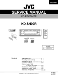
KD-SH99R
SERVICE MANUAL
CD RECEIVER
KD-SH99R
Detachable
ATT
ANGLE
EQ
CD
FM
AM
RD
CH
AUX
SEL
VOLUME
RM-RK100
Area Suffix
E ------- Continental Europe
EX ----- Central Europe
Contents
Safety precaution
Preventing static electricity
Disassembly method
Adjustment method
Flow unit reading TOC
of CD/CD-R/CD-RW
Maintenance of laser pickup
Replacement of laser pickup
Description of major ICs
COPYRIGHT
2001 VICTOR COMPANY OF JAPAN, LTD.
1- 2
1- 3
1- 4
1-15
1-18
1-20
1-20
1-21~45
No.49645
Jun. 2001
KD-SH99R
Safety precaution
1-2
!
Burrs formed during molding may be left over on some parts of the chassis. Therefore,
pay attention to such burrs in the case of preforming repair of this system.
!
Please use enough caution not to see the beam directly or touch it in case of an
adjustment or operation check.
KD-SH99R
Preventing static electricity
1.Grounding to prevent damage by static electricity
Electrostatic discharge (ESD), which occurs when static electricity stored in the body, fabric, etc. is discharged,
can destroy the laser diode in the traverse unit (optical pickup). Take care to prevent this when performing repairs.
2.About the earth processing for the destruction prevention by static electricity
Static electricity in the work area can destroy the optical pickup (laser diode) in devices such as CD players.
Be careful to use proper grounding in the area where repairs are being performed.
2-1 Ground the workbench
Ground the workbench by laying conductive material (such as a conductive sheet) or an iron plate over
it before placing the traverse unit (optical pickup) on it.
2-2 Ground yourself
Use an anti-static wrist strap to release any static electricity built up in your body.
(caption)
Anti-static wrist strap
3. Handling the optical pickup
Conductive material
(conductive sheet) or iron plate
1. In order to maintain quality during transport and before installation, both sides of the laser diode on the
replacement optical pickup are shorted. After replacement, return the shorted parts to their original condition.
(Refer to the text.)
2. Do not use a tester to check the condition of the laser diode in the optical pickup. The tester's internal power
source can easily destroy the laser diode.
4.Handling the traverse unit (optical pickup)
1. Do not subject the traverse unit (optical pickup) to strong shocks, as it is a sensitive, complex unit.
2. Cut off the shorted part of the flexible cable using nippers, etc. after replacing the optical pickup. For specific
details, refer to the replacement procedure in the text. Remove the anti-static pin when replacing the traverse
unit. Be careful not to take too long a time when attaching it to the connector.
3. Handle the flexible cable carefully as it may break when subjected to strong force.
4. It is not possible to adjust the semi-fixed resistor that adjusts the laser power. Do not turn it
Damper bracket
Attention when traverse unit is decomposed
CD mechanism ass’y
*Please refer to "Disassembly method" in the text for pick-up and how to
detach the substrate.
1.Solder is put up before the card wire is removed from connector on
the CD substrate as shown in Figure.
(When the wire is removed without putting up solder, the CD pick-up
assembly might destroy.)
2.Please remove solder after connecting the card wire with
when you install picking up in the substrate.
CD mechanism
control board
Front bracket
FD screw
Feed motor ass’y
Soldering
FD gear
Pickup unit
1-3
KD-SH99R
Disassembly method
Front panel assembly
Removing the front panel assembly
(See Fig.1)
1. Press the release button in the lower right part of the
front panel assembly to unlock.
2. Remove the front panel assembly in the direction of
the arrow.
Release button
Fig.1
Front panel assembly
Removing the top chassis
(See Fig.2 to 6)
Top chassis
Eject button
Turn on power.
1. Press the eject button in the upper left part of the
front panel assembly to move the assembly as
shown in Fig.2 and turn off power.
2. Remove the two screws A on the upper side of the
body.
Fig.2
Top chassis
A
A
Front panel assembly
Fig.3
1-4
KD-SH99R
3. Remove the three screws B on both sides of the
body.
Top chassis
4. Remove the screw C and the three screws D on the
left side of the body.
5. Remove the two screws E and the screw F on the
back of the body.
6. Move the top chassis upward and remove it with the
CD mechanism assembly. The connector on the CD
mechanism assembly is disconnected from
connector CN601 on the main board.
B
B
Fig.4
Top chassis
C
Heat sink
D
B
Fig.5
E
F
Fig.6
1-5
KD-SH99R
Removing the CD mechanism assembly
(See Fig.7)
G
Top chassis
Prior to performing the following procedure, remove
the top chassis.
1. Remove the three screws G inside the top chassis
and remove the CD mechanisma ssembly.
G
G
Removing the motor assembly
(See Fig.8 to 10)
CD mechanisma ssembly
Fig.7
Prior to performing the following procedure, remove
the top chassis.
Motor braket
Spring
1. Disconnect the wire from connector CN703 on the
main board.
2. Remove the motor bracket and the spring attached
to the arm braket assembly (R).
3. Remove the two screws H
bracket.
attaching the motor
4. Remove the washer attaching the clutch assembly
and pull out the clutch assembly from the shaft.
5. Remove the two screws I and the motor assembly
from the motor bracket.
Motor assembly
Arm braket assembly (R)
Fig.8
Main board
Motor braket
CN703
CN601
Clutch assembly
Motor assembly
H
Motor braket
H
R
Washer
Fig.10
1-6
Fig.9
KD-SH99R
Removing the main board
(See Fig.11 to 15)
L
Main board
L
Prior to performing the following procedures, remove
the top chassis and the motor bracket.
1. Disconnect the flexible wire from connector CN701
and CN702 on the main board respectively.
2. Move the front bracket backward until it stops.
3. Remove the four screws J attaching the arm
brackets (L) and (R). Move the right and arm lefter
brackets from the rod gear.
Arm
brackets (R)
J
Arm
brackets (L)
J
J
4. Remove the rod gear.
5. Remove the screw K attaching the rear panel to the
bottom cover on the back of the body.
CN701
CN702
Rod gear
Fig.11
Arm brackets (L)
Arm brackets (R)
Main board
Rod gear
Fig.12
Rear panel
K
Bottom cover
Fig.13
1-7
KD-SH99R
6. Remove the two screws L and move the main board
backwards to release the two joints a. (The main
board will be removed with the rear panel and the
rear heat sink)
Joint a
Joint a
Main board
7. Remove the screw M and N attaching the rear heat
sink.
8. Remove the three screws O and the screw P
attaching the rear panel. Remove the main board.
Fig.14
M
O
Rear panel
P
Rear heat sink
N
Fig.15
Bottom cover
Removing the lifter switch board
(See Fig.16)
Prior to performing the following procedures, remove
the top chassis, the motor bracket and the main
board.
Lifter switch board
1. Remove the two screws Q attaching the lifter switch
board.
Q
Fig.16
1-8
KD-SH99R
Removing the lifter board
(See Fig.17 to 23)
Main board
Prior to performing the following procedure, remove
the top chassis assembly and thefront panel
assembly.
1. Disconnect the flexible wire from connector CN702
on the main board.
2. Remove the four screws R attaching the front
bracket on both sides of the body.
3. Push the pin of the joint c on the front of the front
bracket to release the lock lever.
CN702
Front bracket
Fig.17
Front bracket
R
Fig.18
Joint c
Front bracket
Lock lever
R
Front bracket
Fig.20
Fig.19
1-9
KD-SH99R
4. Remove the screw S attaching the lifter board cover
in the rear of the front bracket.
Joints e
Joints e
Lifter board cover
Joint d
5. Release the two joints d while pushing the front side.
Move the lifter board cover inthe direction of the
arrow and release the eight joints e.
6. Remove the two screws T attaching the lifter board
on the front of the body.
Joint d
S
Joint e
Joints e
Front bracket
Fig.21
Lifter board
Lifter board cover
Fig.22
Fig.23
1-10
T
KD-SH99R
<Front panel assembly>
Prior to performing the following procedure, remove
the front panel assembly.
Removing the front board
(See Fig.24 and 25)
Rear panel
U
U
1. Remove the four screws U attaching the rear panel
to the front panel assembly.
Joint f
U
11
Fig.24
2. Release the eleven joints f of the front panel and the
rear panel.
3. Disconnect the wire from connector CN503 on the
front board.
U
V
Front board Soldering
(CN502)
Soldering
W
Volume board
4. If necessary, unsolder connector CN502 on the front
board.
Removing the volume board
(See Fig.25 and 26)
W
Line in board
CN503
V
Fig.25
Prior to performing the following procedure, remove
the rear panel.
1. Remove the two screws W
board.
attaching the volume
2. Disconnect the volume knob, ring lens and volume
ring from the volume board.
3. If necessary, unsolder the volume board.
Volume board
Volume lens, Volume ring
Removing the line in board
(See Fig.25 and 27)
Rng knob
Fig.26
Prior to performing the following procedure, remove
the rear panel.
1. Disconnect the wire from connector CN503 on the
front board.
Line in board
2. Pull out the line in board from the front panel
assembly.
Fig.25
1-11
KD-SH99R
<CD mechanism section>
CD mechanism assembly
Damper bracket
D
D
Removing the CD mechanism control
board (See Fig.1 and 2)
a
h
h
c
1. Unsolder the part a and b on the CD mechanism
control board.
D
2. Remove the stator fixing the CD mechanism control
board and the damper bracket (To remove the stator
smoothly, pick up the center part).
d
3. Remove the screw A attaching the CD mechanism
control board.
Front bracket
4. Remove the CD mechanism control board in the
direction of the arrow while releasing it from the two
damper bracket slots d and the front bracket slot e.
A
CD mechanism
control board
e
b
Fig.1
Pickup unit
5. Disconnect the flexible wire from connector on the
pickup unit.
Flexible wire
ATTENTION: Turn the FD gear in the direction of the
arrow to move the entire pickup unit to
the appropriate position where the
flexible wire of the CD mechanism unit
can be disconnected easily.
(Refer to Fig.2)
Shift the lock
FD gear
Fig.2
CD mechanism control board
Removing the loading motor
(See Fig.3 to 5)
Prior to performing the following procedure, remove
the CD mechanism control board.
1. Remove the two springs f attaching the CD
mechanism assembly and the front bracket.
2. Remove the two screws B and the front bracket
while pulling the flame outward.
3. Remove the belt and the screw C from the loading
motor.
f
f
B
B
Loading motor
Front bracket
Fig.3
Loading motor
C
Pull outward
Front bracket
Belt
Fig.5
1-12
Flame
Fig.4
Pull outward
KD-SH99R
Removing the CD mechanism assembly
(See Fig.1, 6 to 9)
CD mechanism assembly
D
D
a
h
Prior to performing the following procedure, remove
the CD mechanism control board and the front
bracket (loading motor).
1. Remove the three screws D
bracket.
Damper bracket
h
c
D
and the damper
d
2. Raise the both sides fix arms and move the fix plates
in the direction of the arrow to place the four shafts g
as shown in Fig.8 and 9.
3. Remove the CD mechanism assembly and the two
springs h attaching the flame.
A
Front bracket
CD mechanism
control board
e
b
Fig.1
4. Remove the two screws E and both sides rear
damper brackets from the dampers. Detach the CD
mechanism assembly from the left side to the right
side.
CD mechanism assembly
Damper bracket
D
h
ATTENTION: The CD mechanism assembly can be
removed if only the rear damper
bracket on the left side is removed.
Flame
h
D
D
Fig.6
D
Fig.7
Rear damper bracket
Fix arm (L)
E
Fix plate (L)
g
g
Damper
Fig.8
Rear damper bracket
Fix arm (R)
E
Fix plate(R)
g
g
Damper
Fig.9
1-13
KD-SH99R
Removing the feed motor assembly
(See Fig.10)
Prior to performing the following procedure, remove
the CD mechanism control board, the front bracket
(loading motor) and the CD mechanism assembly.
1. Remove the two screws F
assembly.
FD screw
Part i
Feed motor assembly
Part j
F
and the feed motor
Pickup unit
FD gear
Removing the pickup unit
(See Fig.10 and 11)
Prior to performing the following procedure, remove
the CD mechanism control board, the front bracket
(loading motor), the CD mechanism assembly and
the feed motor assembly.
Pickup unit
Fig.10
G
Nut push spring plate
Pickup mount nut
1. Detach the FD gear part of the pickup unit upward.
Then remove the pickup unit while pulling out the
part i of the FD screw.
Pickup unit
FD screw
ATTENTION: When reattaching the pickup unit,
reattach the part j of the pickup unit,
then the part i of the FD screw.
Fig.11
2. Remove the screw G attaching the nut push spring
plate and the pickup mount nut from the pickup unit.
Pull out the FD screw.
k
k
Removing the spindle motor
(See Fig.12 and 13)
Prior to performing the following procedure, remove
the CD mechanism control board, the front bracket
(loading motor), the CD mechanism assembly and
the feed motor assembly.
1. Turn up the CD mechanism assembly and remove
the two springs k on both sides of the clamper arms.
Open the clamper arm upward.
Fig.12
H
Spindle motor
2. Turn the turn table, and remove the two screws H
and the spindle motor.
H
Fig.13
1-14
KD-SH99R
Adjustment method
Test instruments required for adjustment
1. Digital oscilloscope (100MHz)
2. AM Standard signal generator
3. FM Standard signal generator
4. Stereo modulator
5. Electric voltmeter
6. Digital tester
7. Tracking offset meter
8. Test Disc JVC :CTS-1000
9. Extension cable for check
EXTGS004-26P 1
Standard volume position
Balance and Bass &Treble volume : lndication"0"
Loudness : OFF
BBE
: OFF
Frequency Band
FM 87.5MHz ~107.9MHz(with channel interval set to 200kHz)
FM 87.5MHz 108.0 MHz(with channnel interval set to 50kHz)
AM 530kHz ~ 1710 kHz(with channel interval set to 10kHz)
AM 531 kHz 1602 kHz(with channel interval set to 9 kHz)
Dummy load
Exclusive dummy load should be used for AM,and FM. For
FM dummy load,there is a loss of 6dB between SSG output
and antenna input.The loss of 6dB need not be considered
since direct reading of figures are applied in this working
standard.
Standard measuring conditions
Power supply voltage DC14.4V(11 V to 16V allowance)
Load impedance 4 (4 to 8 allowance)
Line-Out Level/Impedance 4.0V/20k load(fuull scall)
How to connect the extension cable for adjusting
EXTLX003-20P
EXTGS004-26P
EXTLX003-7P
EXTLX003-20PC
EXTLX003-7PC
EXTLX003-2P
1-15
KD-SH99R
< Service mode >
The menu in the service mode can be switched with UP/DOWN.
The menu selected by the SEL button input is executed.
The ordinary mode
"UP" + "DOWN" + VR counterclockwise rotation.
DEL EEPROM
EEPROM data all clear (changer is connected).
CH CH ERR
CD changer error career call (changer is connected).
DELL CH ERR
CD changer EEPROM clear (EEPROM career)
RUNNING CD
CD running mode (Do not use in service).
RUNNING SH
Running mode of front panel (Do not use in service).
DEL DATA
CD ERROR MECHA ERR error career deletion.
CD ADJ R
Self adjustment value call (It is a display switch with VR).
MEKACON WR
Sub-microcomputer writing (Do not use in service).
TEMP DATA
Temperature data call.
VERSION
Microcomputer version confirmation.
The display changes in the up/down key.
The main microcomputer : SH99 J203
The Sub-microcomputer : SH99S 122
CD ERROR
CD relation error career reading
< Error display >
Item
DISC_ERROR_0
DISC_ERROR_1
DISC_ERROR_2
DISC_ERROR_3
DISC_ERROR_4
DISC_ERROR_5
EJECT_ERR
MECHA ERR
1-16
Content
Others
FOCUS NG
Self adjustment NG
CLV NG
TOC reading NG
or
MP3 FILE CHECK NG
BLANK DISC
Panel relation error career reading
KD-SH99R
<ERROR CODE of Panel mechanism>
Memory to EEPROM of 6 digits, 1st and 2nd digit are indicate the operation mode when occur the error,
3rd to 6th digit are indicate details of error.
LCD indication time is use lower 2digits of details of error.
This series is indicate ERR XX (XX is error code).
<ex.> When details of error is 0A0001 , it is indicate ERR 01, details of error is 0E0031 , it is ERR 31.
Switch is from this side sequentially PSW1, PSW2,.....PSW6.
Details of error
1. Error of door open (fault of PSW1)
(1) Time out by PSW1 not changed
(2) PSW1 change during waiting 300ms after open position detected
2. Error of door close (fault of PSW6)
(1) Time out by PSW6 not changed
(2) PSW6 change during waiting 300ms after close position detected
3. Error of shift to DETACH position (fault of PSW5)
(1) Time out by PSW5 not changed to open side
(2) Shift to open side, pass the DETACH position then detect ANGLE1
(3) Time out by PSW5 not changed to close side
(4) Shift to close side, pass the DETACH position then detect close position
4. Error of angle adjustment
4-1 Shift to ANGLE1 (fault of PSW4)
(1) Time out by PSW4 not changed to shift for open side
(2) Shift to open side, pass the ANGLE1 then detect ANGLE2
(3) Time out by PSW4 not changed to shift for close side
(4) Shift to close side, pass the ANGLE1 then detect DETACH position
4-2 Shift to ANGLE2 (fault PSW3)
(1) Time out by PSW3 not change to shift for open side
(2) Shift to open side, pass the ANGLE2 then detect ANGLE3
(3) Time out by PSW3 not changed to shift for close side
(4) Shift to close side, pass the ANGLE2 then detect ANGLE1
4-3 Shift to ANGLE3 (fault PSW2)
(1) Time out by PSW2 not changed to shift for open side
(2) Shift to open side, pass the ANGLE3 then detect OPEN position
(3) Time out by PSW2 not changed for shift for close side
(4) Shift to close side, pass the ANGLE3 then detect ANGLE2
5. PSW fault condition at initialize
When all PSW is checked immediately after RESET, and the state of SWITCH which
cannot be originally is detected, it is displayed as ERR 00.
Error code
0A0001
0A0002
0B0006
0B0007
0C0011
0C0012
0C0013
0C0014
0D0021
0D0022
0D0023
0D0024
0E0031
0E0032
0E0033
0E0034
0F0041
0F0042
0F0043
0F0044
000000
1-17
KD-SH99R
Flow until reading TOC of CD/CD-R/CD-RW
FEED RETURN
Becomes DRVMUTE=H and the output of the IC604 driver becomes possible.
Picking up is moved to surroundings on the inside until becoming REST SW=L.
Afterward, moves in the direction of outer again and stops in the place in which
became REST SW=H.
OFFSET SELF ADJUSTMENT
FOCUS OFFSET, TRACKING OFFSET, and RF OFFSET are done, and
OFFSET of RF AMP in IC603 is corrected.
LASER ON
Pre SP KICK
400ms turns the spindle motor before the focus search starts.
LENS UP
FOCUS ON
Lens UP of the pick is done. At this time, S character curve becomes about
2.0Vp-p by CTS-1000.
The down of the lens and FOCUS ONing are made.
Changes into CD-RW MODE, and serches for FOCUS in case of no FOCUS ON
even if FOCUS search(UP DOWN) is done three times.
THE SPINDLE START
The spindle motor is rotated up to the number of necessary rotations.
TRAKING BALANCE
In the state of tracking OFF, do the self adjustment of wavy OFFSET of TE2 to 0.
It takes time to adjust the one with a large gap of the traking balance of picking up.
At this time, the racking error becomes about 2.8Vp-p by CTS-1000.
RF GAIN
In the state of traking OFF, do the self adjustment of the RF level of RF(TP601)
to 1.0-1.2Vp-p. After adjusts,traking ON is done.
FOCUS GAIN
Do th eself adjustment of the gain intersection of the focus servo to 1.2kHz
(300ms).
TRACKING
TOC READING
Do the self adjustment of the gain intersection of the focus servo to 1.2kHz.
(300ms).
Time expands in DISC that the number of total tracks with CD-TEXT is a lot of.
1Tr. HEAD
It is a head of 1Tr., and the reproduction begins.
2.0Vp-p
Shape of waves when based on Vref(TP602)
TE2
TP605
2.8Vp-p
FE
TP603
FEED
TP634
SP0
TP636
1-18
FE : Focus error signal
TE : T Tracking error signla
FEED : FEED deive signal
SPO : Spindle drive signal
KD-SH99R
Adjustment part
CN771
CN301
C964
C967
C998
R962
R964
D986
Q91
R342
R332
R83
R93
IC51
C817
C818
CN703
C650
R618
R615
D111
R163
R765
IC608
C820
IC771
R736
R761
R729
C771 R775
R746 R725
R722
R724
R779
R780
R778
R777
C710
R773
R781
R782
R774
R772
R770
IC802
C819 R835
R723
R721
R720
R719
R717
R832
R830
IC806
IC805
C714
BZ791
R715 R716 R718
R831
IC803
R676
R762 R764
R763
R814 R812
C814
C824
R784
R783
C826
C816
R657
R653
IC804
C852
C851
R654
PP1
B3
R614
TU1
IC703
R709
IC951
C164
C655
C656
C809
C803
C821
R821
R822
R824 R827
C352
C321
C951
R642
R659
R658
R660
R656
Q683
IC605
R655
C679
R619 X602
R651
R672
R673
R674
R675
R838
IC606
C34
C986
D332
R331
C328
D964
C203
R911
C653
C32
R823
C772
R776
R650
R652
C637
R699
R669
C669
C822
C808
R766
D702
R714
R768
IC602
X801
IC701
R759
R702
D723
C725
D730 C722
R798
R923
R924
R606 R603
C708
X701
X702
R797
R623 R648
R646 R628
R626
D795
D796
C713
C791
X601
R930
D722
D721 CN702
R757
R758
IC601
R657
IC804
R654
C852
C851
R650
R652
R839
R617
R616
C657
C812
R641
C654
C676
R665
R666
C162
R649
R662
R633
R627
R647
C687
R840
R690
R693
R694
C642
R697
R629
C633 R630
R667
R668
C161
L622
R639
R698
C635 C632
C631
R651
R672
R673
R674
R675
FEED
IC803
R676
IC806
IC805
X603
C638
C639
BZ791
R637
C53
C7
C639
C721
D724
D725
D726
D727
D728
D729
Q683
R655
C679
R619 X602
IC605
R662
R633
R693
R699
C637
FE
D1
D2
IC961
CN771
C997
C996
C995
C964
B4
C931
C990
C991
C992
C993
R135
D404
C961
C925
R636
R641
R653
R690
R694
C642
R629
R697
R838
IC606
R642
R659
R658
R660
R656
C687
R840
R627
R647
C625
C624
C630
C629
TE
R669
C669
C57
C25
PP2
R954
R625
R645
Main board
(Forward side)
R649
C654
C676
R665
R666
R162 C163
R164 D161
R161 D162
R813 R817
C811 R811
C804
R211
C651
IC604
C686
R691 R663
C5
C103
X603
C638
R637
C91
C55
C451
C952
R111
C161
L622
R639
R691 R663
C640
C636 C634
TE2
Q81
R854
L852
R851
L851 R833
R834
C915
C916
C351
TH951 R713
C651
C686
R698
C635 C632
C631
C633 R630
C628
C327
R232
R231
Q232
Q231
R132
D231
C323
R220
C220
D401
C144
C143
C917
R120
C912
C913
C307
C643
R643
R687 R857
R688 R856
R689
R855
C641
C640
R636
R931
D914
D912
R695
R696
R661
IC603
R329 R325
C928
D416
D412
C922 C921
D410
D414
R237
R238
C948
C947
B1
CN601
R695
R696
R661
IC603
R933
IC604
R631
R644
R624
R932
C643
R643
C452
IC911
C450
C303
C9
C81
C910
R277 IC171 C175
C120
C628
C723
C724
R687 R857
R688 R856
R689
R855
C641
C4
Q34
C978
IC801
C622
R620 R621
C620 C621
C623
C627
C626
C636 C634
C653
C306
C301
C350
CN701
CN601
C2
D11
X51
R877
C945
L1
CN705
Q35
C977
C982
IC322
C332 R341
C334 C333
R330
C304
R941
R944
R686 R679
R685 R680
R684 R681
R683 R682
C622
R620 R621
C620 C621
C623
C626
C627
C965
C305
R211
C117
D701
C971
C962
C302
R942 C308
Q941
C952
R111
J1
IC961
C969
Q983
R437
C273
C173
C403
C406
C310
R144
R134
C142
C350
FOD
C405
C401
C402
R143 R137 C309
R133 R138
C141
C944
D942
R839
R624
R436 R343
C331 R344
R340
C325
R667
R668
C303
C172
C410
C625
C301
C404
C330
R336
R328
R327
IC323
C272
C407
IC301
C927
IC941
C916
C351
R131
Q132 Q131
IC401
D131
C630
C629
C945
C913
C307
R941
R944
C949
C941
R631
R644
R877
C409
R233
R243
C946
C305
Q941
D962
C243
C244
R244
C241 R234 C242
B2
C304
C943
C329
R337
D967
C924
C624
C944
D942
R978
R976
C408
D408
C302
R942 C308
CN302
D961
R977
C968
D402
C451
C352
C321
C144
C143
C142
R961
C926
C450
R134
IC941
Q755
R963
CN901
C961
L961
SPO
TRD
CN901
J1
C923
C901
D403
R276
D409
C242
C241
R246
D911
C401
R305
R301
R175
D411
R176
R333
R275
C212
C912
R943
IC941
D413
C110
R843
R844
C646
C647
C644
C615
Q791
Q636
R632
X603
C612
R852
C616
R640
R601
C726
R607
C619
R608 R609
C603
C613
B16
R604
C604
R605
R602
L601
C605
C609
R860
C601
R926
R613
R612
R611
R610
R929
R928
R859
C863
X801
R861
C617
C618
R853
C614
C878
R876
C861
R791
C791
R638
C860
C862
R792
C606
Q701
R795
R635
X601
R738
R836
B15
C645
C792
R868
R730
R864
C714
C708
X701
R862
BZ791
R794
R793
R747
R748
R742
R741
C706
C715
R706
R705
R703
D711
R842
R837
C671
R671
R677
C678
C866
R664
C680
R678
C853
C815
C825
C805
C826
R692
R670
C841
C876
C864
R710
R755
R841
C112
R177
R912
B8
C49
C816
R869
D963
R866
IC607
R872
R874
R865
R863
R733
R743
R740
R999
R867
R751
R701
C647
R634
C677
R870
C710
R965
C701
C702
C707
C646
X603
C612
C141
C944
D941
C611
C610
CN602
R927
R925
CN704
R922
Main board
(Reverse side)
R638
Q636
R632
C617
C618
C614
R852
C142
Q942
C945
B10
X602
C660
B606
C713
R734
R735
R728
R731
R753
R664
C644
C615
R853
C616
C309
C308
R304
R302
R303
C653
L606
R711
R671
C671
C680
R677
R678
C678
R876
C402
C307
C301
B14
R166
R796
Vref
C645
R635
C941
C302
C303
C913
B13
Q641
C806
L701
C705
C841
D407
Q423
C352
R622
C652
B9
R769
R737
IC702
C943
R146
R142
C161
C703 C704
B15
C310
R145
R141
C808
R707
R708
R670
R351
C350
R165
R871
X702
IC607
Q642
C351
C952
C162
C807
C711
R951
C677
C174
R352
Q161
C804
Q23
B10
C305
C306
C914
C210
B7
C321
R28
C809
R167
R825
C164
C24
R25
C803
R27
R26
R732
R692
R403
C407
R405
C406
D913
R816
R826
C820
R634
R401
C403
C916
R119
R767
D965
X602
R402
R404
C410
C173
R174
C450
C451
R241
R245
C172
C272
C405
C915
C103
R118
Q24
R21
R22
R739
C719
C712
R745
R273
C323
R173
C203
R218
C57
Q22
R23
C48 R726 R727
C22
C21
C23
R24
C337
R961
C987
R219
C25
Q51
PP2
C47
CN703
C942
R242
R815
R32
R985
R435
C52
C51
R53
R92
C46
C92
R34
Q52
C42 C43
R91
C53
Q32
R33
R36
R274
D980
R54 R52
C54
R51
L51
C7
B6
C32
PP1
C408
C273
C325
D415
C409
C175
C452 C918
C910
C911
C5
Q33
R984
Q322
R334
C994
C336
Q977
R913
R55
R3
R2
C8
C56
TU1
D406
D405
B12
C329
C602
C45
C982
D978
R1
C40 C41
R56
B11
R272
R335
C973
R975
X51
C978
R35
Q1
RF
Q979
Q12
B18
R843
R844
R837
R13
R82
C81
C91
R236
R172
Q323
Q321
C977
R81
C6
C44
B14
R970
L961
R235
R178
C962
Q965 R986
R15
R136
CN302
R339
D961
C969
C965
R969
R10
R14
R12
C82
R338
R971
Q966
R968
C967
C966
Q13
Q11
C9
R987
R4
C971
R11
R5
B5
C755
CN705 D754C2
C4
Q986
R754
C774
C3
CN301
C972
C773
C754
C1
B17
C11
C10
C84
C94
R640
C860
1.0
1.2Vp-p
RF shape of waves
1-19
KD-SH99R
Maintenance of laser pickup
(1) Cleaning the pick up lens
Before you replace the pick up, please try to
clean the lens with a alcohol soaked cotton
swab.
(2) Life of the laser diode
When the life of the laser diode has expired,
the following symptoms will appear.
(1) The level of RF output (EFM output:ampli
tude of eye pattern) will be low.
Is RF output
0.8
NO
Replace it.
YES
O.K
Replacement of laser pickup
Turn off the power switch and,disconnect the
power cord from the ac outlet.
(3) Semi-fixed resistor on the APC PC board
The semi-fixed resistor on the APC printed
circuit board which is attached to the pickup
is used to adjust the laser power.Since this
adjustment should be performed to match the
characteristics of the whole optical block,
do not touch the semi-fixed resistor.
If the laser power is lower than the specified
value,the laser diode is almost worn out, and
the laser pickup should be replaced.
If the semi-fixed resistor is adjusted while
the pickup is functioning normally,the laser
pickup may be damaged due to excessive current.
Replace the pickup with a normal one.(Refer
to "Pickup Removal" on the previous page)
Plug the power cord in,and turn the power on.
At this time,check that the laser emits for
about 3seconds and the objective lens moves
up and down.
Note: Do not observe the laser beam directly.
Play a disc.
Check the eye-pattern at measures
between TP601 and TP602.
Finish.
1-20
KD-SH99R
Description of major ICs
UPD784215AGC146(IC701):MAIN CPU
1.Pin layout
75
51
76
50
100
26
1
25
2.Block diagram
INTP2/NMI
INTP0,INTP1
INTP3-INTP6
TI00
TI01
TO0
PROGRAMMABEL
INTERRUPT
CONTROLLER
UART/IOE1
BAUD-RATE
GENERATOR
TIMER/COUNTER
(16 BITS)
UART/IOE2
BAUD-RATE
GENERATOR
TI1
TO1
TIMER/COUNTER1
TI2
TO2
TIMER/COUNTER2
CLOCKED
SERIAL
INTERFACE
(8 BITS)
RxD1/SI1
TxD1/SO1
ASCK1/SCK1
RxD2/SI2
TxD2/SO2
ASCK2/SCK2
SI0
SO0
SCK0
AD0-AD7
(8 BITS)
A0-A7
A8-A15
TI5/TO5
TIMER/COUNTER5
(8 BITS)
TI6/TO6
TIMER/COUNTER6
(8 BITS)
TIMER/COUNTER7
(8 BITS)
PORT 0
TI7/TO7
P00-P06
PORT 1
P10-P17
TIMER/COUNTER8
(8 BITS)
PORT 2
P20-P27
PORT 3
P30-P37
PORT 4
P40-P47
PORT 5
P50-P57
PORT 6
P60-P67
PORT 7
P70-P72
PORT 8
P80-P87
PORT 9
P90-P95
PORT 10
P100-P103
PORT 12
P120-P127
PORT 13
P130,P131
TI8/TO8
WATCH TIMER
WATCHDOG
TIMER
RTP0-RTP7
ANO0
ANO1
AV REF1
AV SS
ANI0-ANI7
AV REF0
AV DD
AV SS
REAL-TIME
OUTPUT PORT
D/A
CONVERTER
BUS I/F
78K/IV
CPU CORE
RAM
RD
WR
WAIT
ASTB
ROM
A/D
CONVERTER
PCL
CLOCK OUTPUT
CONTROL
BUZ
BUZZER OUTPUT
A16-A19
RESET
SYSTEM
CONTROL
X1
X2
XT1
XT2
VDD
VSS
TEST
1-21
KD-SH99R
UPD784215AGC146(1/2)
Pin No.
1
2
3
4
5
6
7
8
9
10
11
12
13
14
15
16
17
18
19
20
21
22
23
24
25
26
27
28
29
30
31
32
33
34
35
36
37
38
39
40
41
42
43
44
45
46
47
48
49
50
1-22
Symbol
PREQ
AMUTE
DIMMER-OUT
ANT PEM
VDD
X2
X1
VSS
XT2
XT1
RESET
I/O
O
O
O
O
O
O
O
O
I
I
RDS-SCK
RDS-DA
REMOCON
AVDD
AVREF0
SD-ST
I
O
I
I
I
I
I
I
MRC DATA
KEY0
KEY1
TEMP
LEVEL
SQ
S.METER
AVSS
INLOCK
NC
AVREF
BUS-SI
BUS-SO
BUS-SCK
(STAGE)
LCD-DA
LCD-CL
LCD-CE
BUZZER
EPDAI
EPDAD
EPCLK
BUS-I/O
PM0
PM1
I
I
I
I
I
I
I
O
O
I
O
I/O
I
O
O
O
O
I
O
O
O
O
O
BUS-INT
PS2
Function
Mechanism power supply ON/OFFdemand output("L":On demand)
Audio output MUTE control signal output ("L" :MUTE ON)
Non connected
Non connected
Non connected
Non connected
Unused output port
Antenna remote output
5V connection
Sub-clock 32.738MHz
Sub-clock 32.738MHz
GND connection
Sub-clock 12.5MHz
Sub-clock 12.5MHz
Reset detection terminal
Non connected
J-BUS signal interrupt input
POWER SAVE2 BACK UP synchronization. It is H input and stop mode.
Unused input port
RDS clock input
RDS data input
Remote control signal input
5V connction
5V connection
Station detector, stereo signal input.
It is H and broadcasting station havingBroadcasting station,L:stereo
MRC DATA input
Key input 0
Key input1
Temperature data input for contrast correction
Level meter input
S.QUALITY level input
S.METER level input
GND connection
The LOCK detection output. At LOCK:H
Unused output port
5V connection
J-BUS data input
J-BUS data output
J-BUS clock I/O
H:L:Initialization port
Data output to LCD driver
Clock output to LCD driver
Chipenable output to LCD driver
Buzzer output
Communication data input of 12C
Communication data input of 12C
Communication data input of 12C
The J-BUS I/O switch output. When outputting :H,When inputting :L
Panel close side motor control signal output
Panel opening side motor control signal output
KD-SH99R
UPD784215AGC146(2/2)
Pin No.
51
52
53
54
Symbol
DETACH
55
56
57
58
59
60
61
62
63
64
65
66
67
68
69
70
71
72
73
74
VCR CONT
PNL SW1
PNL SW2
PNL SW3
PNL SW4
PNL SW5
PNL SW6
AFCK
SEEK/STOP
S MUTE
FM/AM
PLL-CE
PLL-DO
PLL-CLK
PLL-DI
TEL-MUTE
AMP KILL
VSS
DIMMER-IN
PS1
O
I
I
I
I
I
I
O
O
O
O
O
O
O
I
I
O
75
76
77
78
79
80
81
82
83
84
85
86
87
88
POWER
CD-ON
MUTE
W-LPF1
W-LPF2
W-MUTE
VDD
VOL-DA
VOL-CLK
CF-SEL
PMKICK
EMPH
O
O
O
O
O
O
O
O
O
O
O
O
O
I
89
90
91
92
93
94
95
96
97
98
99
100
VOL-2
(J/R)
BUCK
CCE
LSI RST
TEST
VOL-1
(DISC SEL)
SW1
I/O
O
O
O
I
I
I
I
I
O
O
O
O
O
O
O
O
I
Function
Non connected
Non connected
Non connected
The detach signal input. It is L of 200ms or more and operation mode.
It is H and POWER SAVE.
Signal output for VCR control
Panel position detection switch one signal input.
Panel position detection switch two signal input.
Panel position detection switch three signal input.
Panel position detection switch four signal input.
Panel position detection switch five signal input.
Panel position detection switch six signal input
The Af check output. When you check AF:L.
The auto seek stop switch output. At SEEK:H, STOP:L.
Software mute output for CF switch noise.
FM and the AM switch output. At FM:H,At AM:L
CE output for IC control for PLL.
Data output for IC control for PLL.
Clock output for IC control for PLL.
Data input for IC control for PLL.
Telephone ,ute detection input.
POWER-AMP, ON/OFF switch output. H:OFF
GND connection
Dimmer detection input. L:Dimmer ON
At POWER SAVE of POWER SAVE1.ACC and synchronization:L.
When operating :H.
The POWER ON/OFF switch output. At the time of the POWER ON:H.
The CD power supply control signal output. At CD:H.
The mute output. At the time of the MUTE ON:L.
Sub woofer cutoff frequency control output 1
Sub woofer cutoff frequency control output 2
The mute output for the sub woofer. At the time of the MUTE ON:H.
5V connection.
Data output for IC control for electronic volume.
Clock output for IC control electronic volume.
Signal output for FM belt region filter switch.
Signal output for panel motor kick
The CD emphasis output. When turning.At On:H.
Non connected
Pulse which rotation volume pulse signal inputs, and becomes
judgment of change actually.
rotation volume pulse signal input
H:J version and L:R version
Non connected
Non connected
CDLSI reset signal output
GND connection
Non connected
Non connected
Non connected
Non connected
Non connected
Panel SW1
1-23
KD-SH99R
UPD63711AGC(IC603):RF Servo amp
1.Pin layout
144
1
109
108
36
73
37
72
2.Pin function
UPD63711AGC(1/3)
Pin No.
1
2
3
4
Symbol
VSSO
ZRASO
ZCASO
ZCAS1
I/O
O
I
I
5
VSSO
I
6
ZOE
I
7
8
9
ZUWE
ZLWE
VSSO
O
I
I
10
11
12
13
14
15
16
17
18
19
20
21
22
23
24
25
26
27
RA0
RA1
RA2
RA3
RA4
RA5
RA6
RA7
VDD0
VSS0
RA8
IO0
IO1
IO2
IO3
IO4
IO5
VSSO
O
O
O
Function
It is GND of the logic circuit.
It is RFOK signal output terminal.
Reset signal input terminal. (Active row)
Command/parameter identification signal input terminal
A0=L:STB active=Address register set. A0=H:STB active= Parameter set.
The data strove signal input terminal. It is signal to de the latch in LSI as
for the cereal data.
The clock signal input terminal to input and output the cereal data. Input
data from terminal SI is taken by standing up about this signal, and the
cereal data from the terminal SO is output with go down.
The cereal data and the status signal are output.
Cereal data input terminal.
The crystal oscillation control terminal. Please input the reset signal
before stopping the crystal oscillation. Moreover, the crystal oscillation is
steady and input the reset signal, please when moves from the state of
the crystal oscillation stop to the ordinary mode.
XTALEN=L:ordinary mode XTALEN=H:Crystal oscillation stop.
Positive power supply supply terminal to logic circuit.
Positive power supply supply terminal to D/A converter.
R-ch audio signal output terminal.
It is D/A converter GND.
The outside credit capacitor connection terminal for SCF regulator.
It is D/A converter GND.
L-ch audio signal output terminal.
Positive power supply supply terminal to D/A converter.
Output terminal of right channel voice data. PWM output.
O
Left channel voice data audio output terminal. PWM output.
O
I
O
28
IO6
O
29
IO7
I
30
31
IO8
IO9
O
I
32
IO10
O
Positive power supply supply terminal to crystal oscillation circuit.
Crystal departure pendulum connection terminal (Output)
Crystal departure pendulum connection terminal (Input)
It is GND of the crystal oscillation circuit.
Positive power supply supply terminal to logic circuit.
The output terminal of priemphasis information in sub code Q.
When the emphasis is added, high level is output. Polarity can be
switched by the command.
F6H LSB EP=0:Normal output EP=1:Reversing output.
Flag output terminal which shows that data under output is composed by
data which cannot be corrected.(active high)
The cereal data input terminal to building DAC into. When DSP etc. are
not connected with latter part, it should be short with the terminal DOUT.
It is an output terminal of the cereal voice data.
Cereal clock input terminal to building DAC into.
The output voice data changes from DOUT by standing up about this
clock. The system connected with latter part must take data by standing
up about this signal.
The output voice data changes from DOUT by standing up about this
clock.The system connected with latter part must take data by standing
up about this signal.
1-24
KD-SH99R
UPD63711AGC(2/3)
Pin No.
33
34
Symbol
IO11
IO12
I/O
I
O
35
IO13
O
36
37
38
39
40
41
42
VSSO
VDD1
IO14
IO15
DREQ
DRESP
IOP7
O
O
I
O
O
43
IOP6
O
44
IOP5
O
45
46
47
48
49
50
51
52
53
54
55
56
57
58
59
60
61
62
63
64
65
66
IOP4
IOP3
IOP2
IOP1
IOP0
HDBDIR
DVDD
PACK
TSO
TSI
TSCK_B
TSTB_B
DGND
TEST0
TEST1
ATEST
AGND
FD
TD
SD
MD
DACO
O
67
FBAL
O
68
TBAL
O
69
TEVCA
O
70
71
72
73
74
75
76
77
AVDD
EFM
ASY
C3T
RFI
AGCO
AGCI
RFO
O
I
I
O
I
O
O
Function
LRCK signal input terminal to building DAC into.
Signal which distinguishes left channel/right channel of voice data output
from DOUT.
Terminal (88.2kHz)(WDCK)of the output of the frequency signal twice
defect detection output terminal(HOLD) LRCK HOLD/WDCK can be
switched with the microcomputer.
Terminal of output of data of Digital audio interface.
It is GND of the logic circuit.
Buffer ring output terminal of oscillation.
The state of this terminal is output to Bit5 of the status output.
Positive power supply supply terminal to logic circuit.
It is EFM-synchronous detection signal.becomes high-level when the
output of the synchronous pattern detection signal and the frame
counter is corresponding by the EFM recovery part, and becomes a row
level at the disagreement.
Mirror output terminal. (MIRR).It is a frame synchronous signal of PLL
system. The one that a basic frequency (44.1kHz)of the reading signal
obtained in PLL system was divided makes almost equally to the
synchronization(7.35kHz) of one frame. (WFCK)MIRR/WFCK can be
switched with the microcomputer.
the terminal for the monitor of the bit clock. When PLL is locked, the
go down edge of the EFM signal and this signal locks.
it is GND of the logic circuit.
The output terminal which shows the C1 error correction result. Even
go down of RFCK is fixed.
It is an output terminal which shows the C2 error correction result. Even
of RFCK is fixed.
O
O
I
I
I
I
Positive power supply supply terminal to logic circuit.
It is PACK synchronous signal shows the head of packing.
It is a cereal output terminal of the CD-TEXT data.
It is a serial input terminal of the CD-TEXT control parameter.
Cereal clock input terminal of CD-TEXT.
Terminal of input of parameter strove signal of CD-TEXT.
It is GND of the logic circuit.
It is a test terminal. Please connect with GND usually.
O
O
O
O
O
O
It is a test terminal. Please make to the opening usually.
It is GND of an analog circuit.
Focus drive output terminal.
Tracking drive output terminal.
Thread drive output terminal.
Spindle drive output terminal.
It is DAC output terminal for the adjustment. A set value of CRAM7FH is
output.
It is DAC output terminal for the adjustment. A set value of CRAM7CH is
output (built-in RF FE amplifier offeset).
It is DAC output terminal for the adjustment. A set value of CRAM7DH is
output.
It is DAC output terminal for the adjustment. A set value of CRAM7EH is
output (built-in RF TE amplifier offset).
It is a positive power supply supply terminal to an analog circuit.
EFM signal output terminal.
It is a standard voltage input terminal of the EFM comparator.
Capacitor connection terminal for 3T detection.
RF signal input terminal for EFM data generation.
RF signal output terminal after gain is adjusted.
Input terminal of RF-AGC amplifier.
Output terminal of RF saming amplifier.
1-25
KD-SH99R
UPD63711AGC(2/2)
Pin No.
78
79
80
81
82
83
84
85
86
87
88
89
90
91
92
93
94
95
Symbol
EQ2
EQ1
RF
AGND
A
C
B
D
F
E
AVDD
REFOUT
FE
FEO
TE
TEO
TE2
TEC
I/O
-
Function
Equalizer part connection terminal of RF amplifier.
I
I
I
I
I
I
I
O
I
O
I
O
O
I
96
97
AGND
PD
I
98
99
100
LD
PN
AVDD
O
I
-
Reversing input terminal of RF saming amplifier.
It is GND of an analog circuit.
Photo detector A input terminal.
Photo detector B input terminal.
Photo detector C input terminal.
Photo detector D input terminal.
Photo detector F input terminal.
Photo detector E input terminal.
Positive power supply supply terminal to analog circuit.
reference potential output terminal.
Focus make an error amplifier reversing input terminal.
Focus Allah amplifier output terminal.
Tracking make an error amplifier reversing input terminal.
Tracking error amplifier output terminal.
Terminal to which tracking error after amplifies is output.
The tracking comparator input terminal. The tracking error signal which
cuts the DC element is input. The tracking 0 crossing is detected by
using this signal in LSI.
it is GND of an analog circuit.
It is a terminal of the input of the detection signal of PD for the LD output
monitor.
LD control current output terminal.
It is a control polarity set value of the APC circuit.
Positive power supply supply terminal to analog circuit.
TC74VHC157FT-X(IC803):DAC SW
1.Pin lauout
2.Pin function
SELECT 1
1A 2
ASG
1B 3
B
A
1Y 4
Y
B
2A 5
A
Y
2B 6
B
A
2Y 7
YYB
GND 8
16
15
14
13
12
11
10
9
Vcc
INPUTS
ST
SELECT
A
B
4B
H
X
X
X
L
4Y
L
L
L
X
L
3A
L
L
H
X
H
3B
L
H
X
L
L
3Y
L
H
X
H
H
X:Don't Care
1-26
OUTPUT
ST
4A
KD-SH99R
UPD70F3033AC015(IC606):SUB CPU
1.Pin layout
100
76
1
75
25
51
26
50
2.Pin function
Pin No.
1
2
3
4
5
6
7
8
9
10
11
12
13
14
15
16
17
18
19
20
21
22
23
24
25
26
27
28
29
30
31
32
33
34
35
36
37
38
39
40
41
42
43
44
45
46
47
48
49
50
UPD70F3033AC015(1/2)
Symbol
TSI
TSCK
JBSO
JBSI
JBCK
EVDD
EVSS
TSTB
XRESET
MIRR
AO
SO
SI
SCK
WSEN
DSPRST
SWAIT
VPP
SA4
SA5
SA6
I/O
O
O
O
I
I/O
O
O
I
O
I
O
O
O
O
I
O
O
O
STB
DRVMUTE
LOAD1
LOAD2
SA0
SA1
SA2
SA3
RESET
XT1
XT2
O
O
O
O
O
O
O
O
I
I
I
O
O
O
O
O
O
O
I
I/O
I/O
I/O
I/O
VSS
VDD
CLKOUT
WR
----RD
--JBCONT
PON
AD0
AD1
AD2
AD3
Function
CD TEXT control parameter cereal output.
CD TEXT control cereal clock output.
JBUS cereal data output.
JBUS cereal data input.
Cereal clock I/O.
5V(power supply for port for I/O).
GND(GND for port for I/O).
CD TEXT parameter strobe signal output.
LSI reset output.
MIRR signal input(H:Speculer).
Command:/parameter:H switch signal output.
DSP cereal data input.
DSP cereal data input.
DSP cereal data clock output.
Internal CD/DC operation of MP3 operation & beginning.
DSP RESET:L.
WAIT signal input from DECODER.
FLASH writing power supply.
DECODER address passing output.
DECODER address passing output.
DECODER address passing output.
(Non connected)
DSP cereal data latch output.
Servo deriver MUTE control signal output(L:MUTE:ON)
Loading drive.
Loading drive.
DECODER address passing output.
DECODER address passing output.
DECODER address passing output.
DECODER address passing output.
Microcomputer reset terminal(L:Reset)
Sub-clock
Sub-clock
The main clock crystal oscillation machine.
The main clock crystal oscillation machine(20MHz).
5V
GND
Internal system clock output(Non connecte)
DECODER data writing.
(Non connected)
(Non connected)
DECODER data reading.
Address bus enable.
JBUS I/O switch.
Mechanism power supply ON:L.
DECODER I/O data bus
DECODER I/O data bus
DECODER I/O data bus
DECODER I/O data bus
1-27
KD-SH99R
UPD70F3033AC015(2/2)
Pin No.
51
52
53
54
55
56
57
58
59
60
61
62
63
64
65
66
67
68
69
70
71
72
73
74
75
76
77
78
79
80
81
82
83
84
85
86
87
88
89
90
91
92
93
94
95
96
97
98
99
100
1-28
Symbol
AD4
AD5
AD6
AD7
BVDD
BVSS
----------------MD
MC
ML
MP3SEL
PREQ
AMUTE
AVDD
AVSS
AVREF
PDET
SW2
SW3
SW4
REST
RFOK
REQ
EXP
ADIN0
ADIN1
ADIN2
ADIN3
--CONT+B
SW1
PACK
INT0
INT1
JBINT
TESTMODE
12CD
--12CC
RXDO
SID
SIC
TSO
I/O
I/O
I/O
I/O
I/O
O
O
O
O
O
O
O
O
O
O
O
O
O
O
I
I
I
I
I
I
I/O
I
I
I
I
I
O
I
I
I
I
I
I
I
I/O
O
I/O
I
O
O
I
Function
DECODER I/O data bus.
DECODER I/O data bus.
DECODER I/O data bus.
DECODER I/O data bus.
5V
GND
(Non connected)
(Non connected)
(Non connected)
(Non connected)
(Non connected)
(Non connected)
(Non connected)
(Non connected)
DAC mode control data.
DAV mode control clock.
DAC mode control latch.
MP3/CD-DA switch SW L:Cd H:MP3
Mechanism power supply ON/OFF demand output(L:ON demand)
Audio output MUTE control signal output(L:MUTE ON)
5V(Power supply for AD converter)
GND(GND for AD converter)
5V(Standard voltage for AD converter)
BACKUP power supply detection(L:BACKUP power supply ON)
SW2 mechanism switch.
SW3 mechanism switch.
SW4 mechanism switch.
Surroundings position detection switch(L:Surroundings)
RFOK signal input.
Data demand.
H:Export L:For country 8cm CD.
Test key input 0 (A/D input)
Test key input (A/D input of one)
Test key input (A/D input of two)
Test key input (A/D input of three)
(Non connected)
LSI5V ON power supply control signal and JBUS control signal input.
SW1 mechanism switch.
PACK synchronous signal of CD-TEXT.
DECODER interrupt request.
DECODER interrupt request.
J-BUS interrupt signal input.
L: test mode shift.
12C data line.
(Non connected)
12C clock line.
FLASH writing cereal data input.
MP3 cereal data output and FLASH writing cereal data output.
MP3 cereal clock output and FLASH writing cereal clock output.
CD-TEXT data serial input.
KD-SH99R
MAS3507D-QG-G10 (IC806) :MP3 decoder
PI12
SOI
SOD
SOC
PI8
XVDD
XVSS
SID
PI4
SIC
SII
1.Pin layout
36
20
PI15
PI0
37
19
PI16
CLKO
38
18
PI17
PUP
39
17
PI18
WSEN
40
16
PI19
WRDY
41
15
RCS
AVDD
42
14
PR
CLKI
43
13
VSENS
AVSS
44
4
5 6
7
8
12
9 10 11
DCSO
RTW
DCSG
3
POR
1 2
RTR
PI1
EOD
PI14
DCEN
21
VDD
VSS
35
I2CD
PI13
PI2
I2CC
33 32 31 30 29 28 27 26 25 24 23
34
22
TE
PI3
(TOP VIEW)
2.Block diagram
MPEG Bit Stream
Digital Audio Output
Volume
Tone
Control
Sync
Ancillary
Data
MPEG
Decoder
Decoder
Status
to C
Config.Reg.
PIO
Status
Start-up Config.
1-29
KD-SH99R
3.Pin function
MAS3507D-QG-G10(1/2)
Pin no.
Symbol
I/O
1
2
3
4
5
6
7
8
9
10
11
12
13
14
15
16
TE
POR
I2CC
I2CD
VDD
VSS
DCEN
EOD
RTR
RTW
DCSG
DCSO
VSENS
PR
PCS
PI19
I
I
I/O
I/O
Supply
Supply
I
OUT
OUT
OUT
Supply
O
I
IN
IN
IN/OUT
17
PI18
IN/OUT
18
PI17
IN/OUT
19
PI16
IN/OUT
20
PI15
IN/OUT
21
PI14
IN/OUT
22
PI13
IN/OUT
23
PI12
IN/OUT
24
25
26
27
SOD
SOI
SOC
PI18
O
O
O
IN/OUT
28
29
30
31
32
33
XVDD
XVSS
SID
SII
SIC
PI4
Supply
Supply
I
I
I
IN/OUT
34
PI3
IN/OUT
35
PI2
IN/OUT
1-30
Function
Test Enable
Reset, Active Low
I 2 C Clock Line
I 2 C Data Line
Positive Supply for Digital Parts
Ground Supply for Digital Parts
Enable DC/DC Converter or Voltage Supervision
PIO End of DMA, Active Low
PIO Ready to Read, Active Low
PIO Ready to Write, Active Low
DC Converter Transistor Ground
DC Converter Transistor Open Drain
DC Converter Voltage Sense
PIO DMA Request Read/Write
PIO Chip Select, Active Low
PIO Data(19)
i)Demand Pin in SDI mode
ii)data bit(7),MSB in PIO DMA input mode
PIO Data(18)
i)MPEG header bit11-MPEG ID(SDI mode)
ii)data bit(6) in PIO DMA input mode
PIO Data (17)
i)MPEG header bit 12-MPEG ID(SDI mode)
ii)data bit(5) in PIO DMA input mode
PIO Data(16)
i)SIC,alternative input for SIC(SDI mode)
ii)data bit(4) in PIO DMA input mode
PIO Data(15)
i)SII, alternative input for SII(SDI mode)
ii)data bit(3) in PIO DMA input mode
PIO Data(14)
i)SID, alternative input for SID (SDI mode)
ii)data bit(2) in PIO DMA input mode
PIO data(13)
i)MPEG header bit 13-Layer ID (SDI mode)
ii)data bit(1) in PIO DMA input mode
PIO Data (12)
i)MPEG header bit 14-Layer ID (SDI mode)
ii)data bit(0) in PIO DMA input mode
Serial Output Data
Serial Output Frame Identification
Serial Output Clock
Start-up 1) : Clock output scaler on/off
Operation : MPEG CRC error
Positive Supply of Output Buffers
Ground of Output Buffers
Serial Input Data
Serial Input Frame Identification
Serial Input Clock
Start-up 1) : Select SDI/PIODMA input mode
Operation : MPEG-Frame Sync
Start-up 1) : Enable Layer 3 / Disable Layer 3 decoding
Operation : MPE Gheader bit 20(Sampling Frequency)
Start-up 1) : Enable Layer 2 / Disable Layer 2 decoding
Operation : MPEG header bit 21(Sampling Frequency)
KD-SH99R
3.Pin function
MAS3507D-QG-G10(2/2)
Pin no.
Symbol
I/O
36
PI1
IN/OUT
37
P0
IN/OUT
38
39
40
41
CLKO
PUP
WSEN
ERDY
O
O
I
O
42
43
44
AVDD
CLKI
AVSS
Supply
I
Supply
1)
Function
Start-up 1) : SDO Select 32 bit mode / 16 bit I 2 S mode
Operation : MPEG header bit 30(Emphasis)
Start-up 1) : Select Multimedia mode / Broadcast mode
Operation MPEG header bit 31 (Emphasis)
Clock Output (normal 24.576 MHz)
Power Up, i.e.Status of Voltage Supervision
WS Enable : Enable DSP
WSEN=0 : Valid clock input at CLKI
WSEN=1 : Clock synthesizer PLL locked
Supply for Analog Circuits
Clock Input
Ground Supply for Analog Circuits
Start-up configuration see Table 2.7.3. in (1)
BU4066BCFV-X (IC322) : Quad analog switch
1. Pin layout & Block diagram
VDD
14
C1
13
C4
12
I/O4
11
O/I4
10
O/I3
9
I/O3
8
1
2
3
4
5
6
7
I/O1
O/I1
O/I2
I/O2
C2
C3
Vss
1-31
KD-SH99R
LC895199K-ND2(IC601):CD-ROM decoder
1.Pin layout
144
1
109
108
36
73
37
72
2.Pin function
Pin No.
1
2
3
4
5
6
7
8
9
10
11
12
13
14
15
16
17
18
19
20
21
22
23
24
25
26
27
28
29
30
31
32
33
34
35
36
37
38
39
40
41
42
43
44
45
46
47
48
49
50
1-32
LC895199K-ND2(1/3)
Symbol
VSSO
ZRASO
ZCASO
ZCAS1
VSSO
ZOE
ZUWE
ZLWE
VSSO
RA0
RA1
RA2
RA3
RA4
RA5
RA6
RA7
VDD0
VSS0
RA8
IO0
IO1
IO2
IO3
IO4
IO5
VSSO
IO6
IO7
IO8
IO9
IO10
IO11
IO12
IO13
VSSO
VDD1
IO14
IO15
DREQ
DRESP
IOP7
IOP6
IOP5
IOP4
IOP3
IOP2
IOP1
IOP0
HDBDIR
Function
RAS signal output terminal to buffer DRAM
CAS signal output 0 terminal to buffer DRAM(0 is used usually)
CAS signal output terminal 1 to buffer DRAM
Buffer DRAM output enable
Buffer DRAM upper write enable
Buffer DRAM lower write enable
Address signal output terminal to data buffer DRAM
5.0V
Address signal output terminal to data buffer DRAM
Data I/O terminal to data buffer DRAM. With built-in pull-up resistor
Data I/O terminal to data buffer DRAM. With built-in pull-up resistor
3.3V
Data I/O terminal to data buffer DRAM.With buolt-in pull-up resistor
General-purpose I/O port
KD-SH99R
LC895199K-ND2(2/3)
Pin No.
51
52
53
54
55
56
57
58
59
60
61
62
63
64
65
66
67
68
69
70
71
72
73
74
75
76
77
78
79
80
81
82
83
84
85
86
87
88
89
90
91
92
93
94
95
96
97
98
99
100
101
102
103
104
105
106
107
108
109
Symbol
TEST0
XTALCK
XTAL
VDD0
VSS0
MCK
TEST1
DSDATA
DLRCK
DBCK
C2PO
SDATA
BCK
LRCK
EXCK
WFCK
SBSO
SCOR
PLL1
PLL2
PLL3
VSS0
VDD1
ZRESET
MCK3
CSCTRL
ZRO
ZWR
ZCS
SUA0
SUA1
SUA2
SUA3
SUA4
SUA5
SUA6
D0
D1
D2
VDD0
VSS0
D3
D4
D5
D6
D7
ZINTO
ZINT1
ZSMAIT
ZRSTCPU
CSEL
ZHRST
ATPINSEL
ZDASP
ZCS3FX
ZCS1FX
DA2
VSS1
VDD1
Function
The terminal TEST.Please connect with VSS
X'tal oscillation circuit input terminal
X'tal oscillation circuit output terminal
5.0V
1/1,2/2,STOP output terminal of XTALCK
The terminal TEST. Please connet with VSS
DAC output terminal
Terminal for CD-DSP I/F
SUB-CODE I/O terminal
Relation connection of PLL terminal
(It is analog VSS in version LC895199 with built-in PLL)
3.3V (It is analog VDD in version LC895199 with buikt-in PLL)
LSI reset terminal
1/1, 1 /5, 2/5, 1/512, and STOP output terminal of XTALCK
Active Lo and Hi selection terminal on MC(microcontroller) side CS
Reading data of MC(microcontroller) signal input terminal
Writing data of MC(microcontroller) signal input terminal
Register chip selection signal input terminal from MC(microcontroller)
MC(microcontroller) register selection signal terminal
MC(microcontroller) data signal terminal.With buit-in puul-up resistor.
5.0V
MC(microcontroller) data signal terminal. With buit-in pull-up resistor.
Interrupt request signal output terminal to MC(microcontroller)
WAIT signal to MC(microcontroller)
Reset signal to CPU
ATAPI control signal
ATAPi data bus
Terminal ATAPI arrangement select terminal. Connects with VDD0
ATAPI data bus
3.3V
1-33
KD-SH99R
LC895199K-ND2(3/3)
Pin No.
110
111
112
113
114
115
116
117
118
119
120
121
122
123
124
125
126
127
128
129
130
131
132
133
134
135
136
137
138
139
140
141
142
143
144
1-34
Symbol
DAO
ZPDIAG
DA1
ZIOCS16
HITRQ
ZDMACK
VSS1
IORDY
ZDIOR
ZDIOR
DMARQ
VSS1
DD15
DDO
DD14
DD1
VDDO
VSS1
DD13
DD2
DD12
DD3
VSS1
DD11
DD4
DD10
VSS1
VDD0
DD5
DD9
DD6
VSS1
DD8
DD7
VDD1
Function
ATAPI data bus
ATAPI data bus
ATAPi data bus
ATAPi control signal
ATAPI control signal
5.0V
ATAPI control signal
ATAPI control signal
5.0V
ATAPI control signal
3.3V
KD-SH99R
HA13164 (IC961) : Regulator
MEMORY
1.Pin layout
1 2 3 4 5 6 7 8 9 10 11 12 13 14 15
2.Block diagram
+B
C1
100u
C2
0.1u
ACC
VCC
8
3
ACC
BATT.DET OUT
9
ANT OUT
2
Surge Protector
C3
0.1u
EXT OUT
1
BIAS
6
TSD
COMPOUT
C4
0.1u
4
ANT CTRL
VDD OUT
7
CTRL
CD OUT
C7
0.1u
11
5
SW5VOUT
12
C5
0.1u
AUDIO OUT
ILMOUT
10
14
C8
0.1u
C6
10u
15
GND
13
R1
ILM AJ
UNIT R:
C:F
note1) TAB (header of IC)
connected to GND
3.Pin function
Pin No.
1
2
3
4
5
6
7
8
9
10
11
12
13
14
15
Symbol
EXT
ANT
ACC
VDD
SW5V
ACC5V
ANT CTRL
MEMORY
BATT DET
9V
CTRL
CD8V
AJ
ILMI
GND
Function
Output voltage is VCC-1 V when M or H level applied to CTRL pin.
Output voltage is VCC-1 V when M or H level to CTRL pin and H level
to ANT-CTRL.
Connected to ACC.
Regular 5.7V.
Output voltage is 5V when M or H level applies to CTRL pin.
Output for ACC detector.
L:ANT output OFF , H:ANT output ON
Connected to VCC.
Low battery detect.
Output voltage is 9V when M or H level applied to CTRL pin.
L:BIAS OFF, M:BIAS ON, H:CD ON
Output voltage is 8V when H level applied to CTRL pin.
Adjustment pin for ILM output voltage.
Output voltage is 10V when M or H level applies to CTRL pin.
Connected to GND.
1-35
KD-SH99R
LC75878W (IC501) : LCD driver
1. Pin layout
100 ~ 76
1
75
~
~
25
51
COMMON
DRIVER
GENERAL
PORT
SEGMENT DRIVER & LATCH
CONTROL
REGISTER
CLOCK
GENERATOR
OSC
S1
COM8
COM1
P4
P1
2. Block diagram
S75/COM9
S74/COM10
S73
26 ~ 50
VLCD
CONTRAST
ADJUSTER
SHIFT REGISTER
VLCD0
VLCD1
CCB
INTERFACE
VLCD2
VLCD3
CE
CL
DI
INH
VLCD4
VDD
VSS
3. Pin function
No.
1~73
74
75
76~83
84~87
88
89
90
91
92
93
94
95
96
97
98
99
100
1-36
Symbol
SEG1~SEG73
SEG74
SEG75
COM8~COM1
P1~P4
VDD
VLCD
VLCD0
VLCD1
VLCD2
VLCD3
VLCD4
VSS
OSC
LCD RESET
CE
CL
DI
I/O
O
O
O
O
O
O
I
I
I
I
I/O
I
I
I
I
Function
Segment driver output pin.
Segment driver output pin.
Segment driver output pin.
Common driver output pin.
General-purpose output pin.
Logic block power supply pin.
LCD driver power supply pin.
LCD driver bias 4/4 voltage (H-level) power pin.
LCD driver bias 3/4 voltage (intermediate level) power pin.
LCD driver bias 2/4 voltage (intermediate level) power pin.
LCD driver bias 1/4 voltage (intermediate level) power pin.
LCD driver bias 0/4 voltage (L-level) power pin.
Power supply pin to connect to ground.
Oscillator pin.
Display off, general-purpose output port L fixed input pin.
Chip enable
Synchronization clock
Transfer data
KD-SH99R
M61508FP-X (IC911) : E. volume
1. Pin layout & Block diagram
36
35
34
33
32
31
30
29
28
27
50K
26
25
24
23
22
21
20
19
LOUDNESS
VDO
(Digital)
+
VCC
(Anarog)
3BAND TONE CONTROL
(BASS/MID/TREBLE)
Soft select
REF
A
B
B
Zero detect
Select SW
I/F
12dB
Z E R O C RO S S
D E T E C TO R
12dB
Z E R O C RO S S
D E T E C TO R
A
TIMER
DETECTOR
LOUDNESS
+
3BAND TONE CONTROL
(BASS/MID/TREBLE)
1
2
3
4
2. Pin function
Pin No.
Symbol
REF
1
DEFP IN1
2
DEFN IN1
3
INA1
4
INB1
5
INC1
6
IND1
7
DEFN OUT1
8
SEL OUT1
9
VOL IN1
10
TONE OUT1
11
FADER IN1
12
REAR OUT1
13
FRONT OUT1
14
15 NonFader OUT1
GND
16
DATA
17
VDDOUT1
18
VDDOUT2
19
CLOCK
20
VDD
21
22 NonFader OUT2
FRONT OUT2
23
REAR OUT2
24
FADER IN2
25
TONE OUT2
26
VOL IN2
27
SEL OUT2
28
DEFN OUT1
29
IND2
30
INC2
31
INB2
32
INA2
33
DEFN IN1
34
DEFP IN1
35
VCC
36
5
6
7
8
9
10
GND
11
12
13
14
15
16
17
18
Function
Grand for IC signal
Differential motion amp. Positive terminal
Differential motion amp. Negative terminal
Input terminal of input selector switch channel 1
Input terminal of input selector switch channel 1
Input terminal of input selector switch channel 1
Input terminal of input selector switch channel 1
Differential output terminal (-)
Input selector output terminal
Volume 1 input terminal
Tone output terminal
Volume 2 input terminal
Fader volume control (Rear) output terminal
Fader volume control (Front) output terminal
Non fader volume output terminal
GND terminal
Control data input terminal
Test terminal
Test terminal
Clock input terminal for serial data transport
Power supply terminal for digital
Non fader volume control output terminal
Fader volume (Front) output terminal
Fader volume (Rear) output terminal
Volume 2 input terminal
Tone output terminal
Volume 1 input terminal
Input selector output terminal
Differential output terminal (-)
Input terminal of input selector switch channel 2
Input terminal of input selector switch channel 2
Input terminal of input selector switch channel 2
Input terminal of input selector switch channel 2
Differential motion amp negative input terminal
Differential motion amp positive input terminal
Power supply terminal
1-37
KD-SH99R
IN5-
IN5+
IN4+
IN4-
OUT4
MUTE2
SS,GND
VREF
VREFO
OUT5
MUTE1
VM5-
IN2+
VM3+
VM5+
VM3-
VM1+
IN2-
N.C
VM1-
VM4-
IN3+
OUT1
OUT2
Vm2
IN1-
VM4+
VBS2
Vm1
VM2-
IN3-
VBS1
VM2+
OUT3
IN1+
GND
CH3IN
REG+
REGB
1.Pin layout
GND
M63008FP-X (IC604) : 5ch Actuator driver
2.Block diagram
Vm1
VBS1
5
VBS2
Vm2
39
38
4
VBS2
IN1+
IN1OUT1
3
6
VM1(+)
9
VM1(-)
8
VBS1
E1
7
R
R
Vm1
R
Vm2
R
VBS1
VBS2
CH1
X5
Vrefm2
Vrefm1
VBS1
VM2(+)
12
VM2(-)
13
OUT2
14
IN2-I
IN2+
15
VREFO
CH2
X5
VREFO
BIAS
VBS1
E2
SLEEP
21
35
VM3(-)
31
VM4(+)
30
VM4(-)
23
22
IN4IN4+
OUT4
29
VM5(+)
28
vm5(-)
26
25
IN5IN5+
OUT5
24
VBS2
20
CH5
X8
MUTE ON
VREF
1~4
CH
5CH
TSD
1.25V
VBS2
2
E5
1
19
17
MUTE1
SS,GND
1-38
VM3(+)
Low,Open
VREG
REG+
CH4
X8
E4
16
34
37
41
HI :Sleep
VBS1
VBS2
REGB
CH3
X8
42
IN3IN3+
OUT3
CH3 IN
40
VBS2
VBS1
VREF
E3
18
10 11 32 33
MUTE2
GND (4PIN)
27
KD-SH99R
28
15
1
14
2. Block diagram
BCK
Serial
LBCK
Input
DATA
I/F
Vcc2R
AGND2R
1. Pin layout
Vcc2L
AGND2L
PCM1716E-X (IC802) : D/A converter
Low-pass
Filter
DAC
Mult-level
8X Oversampling
EXTL
Delta-Sigma
Digital Filter
Modulator
with
ML/llS
MC/DM1
MD/DM0
CS/WO
MODE
MUTE
RST
1
2
3
4
5
6
7
8
9
10
11
12
13
14
15
16
17
18
19
20
21
22
23
24
25
26
27
28
Symbol
LRCK
DATA
BCK
CLKO
XTI
XTO
DGND
VDD
VDD2R
AGND2R
EXTR
NC
VOUTR
AGND1
Vcc1
VOUTL
NC
EXTL
AGND2L
Vcc2L
ZERO
RST
CS/IWO
MODE
MUTE
MD/DM0
MC/DM1
ML/IIS
Low-pass
Filter
DAC
VoutR
EXTR
Function Controller
Mode
ZERO
Control
I/F
BPZ-Cont
SCK
Crystal OSC
XTI
3. Pin function
Pin
No.
VoutL
I/O
I
I
I
O
I
O
O
O
O
O
O
I
I
I
I
I
I
I
XTO
Open drain
Power Supply
CLKO
Vcc1 AGND1
Vcc DGND
Function
LRCK clock input
Serial audio data input
Bit clock input for serial audio data
Buffered output of system clock
Oscillator input / External clock input
Oscillator output
Digital ground
Digital power +5V
Analog power +5V
Analog ground
Rch common pin of analog output amp
Non connection
Rch analog voltage output of audio signal
Analog ground
Analog power +5V
Lch analog voltage output of audio signal
Non connection
Lch common pin of analog output amp
Analog ground
Analog power +5V
Zero data flag
Reset
Chip select / Input format selection
Mode control select
Mute control
Mode control, Data / De-emphasis selection 1
Mode control, BCK / De-emphasis selection 2
Mode control, WDCK / Input format selection
1-39
KD-SH99R
SAA6579T-X(IC51):RDS
1.Pin layout
QUAL
1
16 RDCL
RDDA
2
15 T57
Vref
3
14 OSCO
MUX
4
13 OSCI
VODA
5
12 V0DD
VSSA
6
11 VSSD
CIN
7
10 TEST
SCOUT
8
9
MODE
2.Block diagram
13
ANTIALIASING
FILTER
4
57 kHz
BANDPASS
(8th ORDER)
14
OSCILATOR
AND
DIVIDER
RECONSTRUCTION
FILTER
12
QUALITY BIT
GENERATOR
1
8
7
CLOCKED
COMPARATOR
5
3
BIPHASE
SYMBOL
DECODER
COSTAS LOOP
VARIABLE AND
FIXED DIVIDER
DIFFERENTIAL 2
DECODER
15
VP1
REFERENCE
VOLTAGE
CLOCK
REGERATION
AND SYNC
15
TEST LOGIC AND OUTPUT
SELECTOR SWITCH
6
9
10
11
3.Pin function
1-40
Pin No.
Symbol
Description
1
QUAL
Quality indication output
2
RDDA
RDS data output
3
Vref
Reference voltage output (0.5VDDA)
4
MUX
Multiolex signal input
5
VDDA
+5V supply voltage for analog part
6
VSSA
Ground for analog part (0V)
7
CIN
Subcarrier input to comparator
8
SCOUT
Subcarrier output of reconstruction filter
9
MODE
Oscllator mode / test control input
10
TEST
Test enable input
11
VSSD
Ground for digital part (0V)
12
VDDD
+5V supply voltage for digital part
13
OSCI
Oscillator input
14
OSCO
Oscillator output
15
T57
57 kHz clock signal output
16
RDCL
RDS clock output
KD-SH99R
BA3220FV-X (IC301,IC401) : Line out amp
1.Pin layout
14
8
3220
1
7
2.Block diagram
CL14
LGND
13
OUTL
12
OUTR
11
RGND
10
CR9
CR+
8
- +
+ -
+ -
- +
+ -
- +
REFR
REFL
FILTER
1
CL+
2
Vcc
3
INL
4
NFL
5
FIL
6
NFR
7
INR
1-41
KD-SH99R
IS41C16256-35T(IC602):RAM
1.Pin layout
44
21
1
22
2.Block diagram
OE
WE
LCAS
UCAS
CAS
CLOCK
GENERATOR
WE
CONTROL
LOGICS
CAS
WE
OE
CONTROL
LOGIC
OE
DATA I/O BUS
COLUMN DECODERS
SENSE AMPLIFIERS
A0-A8
1-42
ADRESS
BUFFERS
ROW DECODER
REFRESH
COUNTER
MEMORY ARRAY
262.144 x 16
DATA I/O BUFFERS
RAS
CLOCK
GENERATOR
RAS
RAS
I/O0-I/O15
KD-SH99R
IC-PST9333U-X (IC702) : Reset IC
1. Pin layout
2. Block diagram
NC
1
NC
4
Vcc
GND
2
GND
3
VOUT
Vcc
NC
4
1
3
VOUT
2
GND
3. Pin function
Pin No.
1
2
3
4
Symbol
NC
GND
VOUT
Vcc
Function
Non connect
GND terminal
Reset signal output terminal
Power supply terminal
1-43
KD-SH99R
NJM4565V-X (IC171,IC951,IC323) : Ope amp
1. Pin layout & Block diagram
2. Pin function
Pin
No.
8
1
2
A
1
2
3
4
5
6
7
8
7
B
3
6
4
8
Function
A output
A-input
A+input
VB+input
B-input
B output
V+
NJM4580V-X (IC801) : CD LPF
1. Pin layout & Block diagram
1
2
2. Pin function
8
A
7
B
3
6
4
8
Pin
No.
Function
1
2
3
4
5
6
7
8
A output
A -input
A +input
VB +input
B -input
B output
V+
RPM6938-SV4 (IC561) : Remote sensor
1.Block diagram
Vcc
AGC
AMP
BPF
PD
Rout
Detector
fo
trimming
circuit
magnetic
1-44
22k
Comp
I/V
conversion
Vcc
shield
GND
KD-SH99R
S-81332HG-KC-X (IC804) : Regulator
2. Block diagram
1. Pin layout
1
2
3
Vout
GND
Vin
VIN 3
VREF
1 VOUT
1
2
3
2
GND
LB1830M-X(IC608):Regulator
2.Block diagram
1.Pin layout
OUT1 Vs OUT2
IN2 IN1 Vm Vm1 Vcont
10
9
8
7
6
VCC
1
2
3
4
5
Vcc OUT2 GND OUT1 Vs
Vref
Logic
Predriver
GND
IN1 IN2 Vm
Vcont Vref
TC74VHC126FT-X(IC605):Buffer
1.Pin layout
2.Function
1G 1
14 Vcc
1A 2
13 4G
INPUTS
G
A
1Y 3
12 4A
L
X
Z
2G 4
11 4Y
H
L
L
H
H
H
2A 5
10 3G
2Y 6
9
3A
GND 7
8
3Y
OUTPUT
Y
X:Don't Care
Z: High impedance
1-45
KD-SH99R
VICTOR COMPANY OF JAPAN, LIMITED
MOBILE ELECTRONICS DIVISION
PERSONAL & MOBILE NETWORK BUSINESS UNIT. 10-1,1Chome,Ohwatari-machi,Maebashi-city,Japan
(No.49645)
200106