1
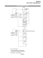
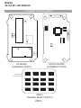
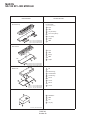
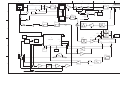
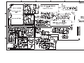
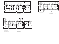
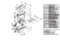
MAXON
SD-125 RF LINK MODULE
ANTENNA SWITCH
LEVEL SHIFTER & CHARGE PUMP
When transmitting, the diodes D5 and D6 are forward biased
enabling the RF signal passage to the antenna. D6 is shorted to
ground inhibiting the RF signal to front end. In receive the
diodes D5 and D6 are reversed biased passing the signal from
the antenna through L13 and C83 to the front end without signal
loss.
The charge pump is used for changing output signals Fr, Fv at
PLL IC from 0-5v to 0-12v necessary for controlling the VCO.
AUTOMATIC CURRENT CONTROL (ACC) CIRCUITS
The ACC circuit consists of R109, variable resistor RV1,
IC3(B) and transistors Q21 and Q22. The supply current is
monitored by the difference voltage on R109 (0.1 Ohm). If the
current varies by RF power output or other reasons, it produces
some bias voltage by IC3A and Q19. The differential signal at
the output of IC3 is passed to Q21 and Q22 that produces a
constant power output to the antenna. RV1 is used to adjust the
RF power level.
RF CIRCUITS PLL SYNTHESIZER
12.8 MHz TCXO
The TCXO contains the 3-stage thermistor network
compensation and crystal oscillator and modulation ports.
Compensation is ±5 PPM or less from -30c to +60c.
PLL IC DUAL MODULES PRESCALER
Input frequency of 12.8 MHz to IC2 MC14519 pin 20 is
divided to 6.25 kHz or 5 kHz by the reference counter, and then
supplied to the comparator. RF signal input from VCO is
divided to 1/64 at the prescaler in IC2, divided by A and N
counter in IC2 to determine frequency steps, and then supplied
to the comparator. PLL comparison frequency is 6.25/5kHz so
that minimum programmable frequency step is 5/6.25 kHz.
The A and N counter is programmed to obtain the desired
frequency by serial data in the CPU. In the comparator, the
phase difference between reference and VCO signal is
compared. When the phase of the reference frequency is
leading , Fv is the output, but when VCO frequency is leading,
Fr is the output. When Fv=Fr, phase detector out is a very small
pulse. 64/65 modulus prescaler is comprised in IC2, and has
two output ports:
•
•
Port A pin 16: TX enable 2
Port B pin 15: prescaler power save control in PLL
IC Pin 13 labeled test2 allows the technician to see
the output of the dual modulus prescaler for trouble
shooting purposes, no connection should be made to
this pin.
REFERENCE FREQUENCY LPF
The Loop Filter contains R12, C21 and C22. LPF settling time
is 12mS with 1 kHz frequency. This also reduces the residual
side-band noise for the best signal-to-noise ratio.
DC TO DC CONVERTER
The DC to DC converter convert the 5v to 14-16v to supply the
necessary voltage for wide range frequency in the VCO.
VCO
The VCO consist of an RX VCO and a TX VCO. It is switched
TX/RX by the power source. It is configured as a colpits
oscillator and connected to the buffer as a cascade bias in order
to save power. The varicap diode D201/D301 are
low-resistance elements and produce a change in frequency
with a change in reverse bias voltage (2-11v). L203/L303 are
resonant coils, which changes the control voltage by the tuning
core. D202 modulation diode, modulates the audio signal.
C204 compensates for the non-linearity of the VCO due to
modulation diode, and maintains a constant modulation
regardless of frequency.
RECEIVER
FRONT-END
The receive signal is routed backward through the low pass
filter, then onward to Pin 1 of the Hybrid Receiver Front End
Module to a bandpass filter consisting of (VHF C622 through
C608, L607 through L604 ) and (UHF C601through C610,
L601 through L603 ) is coupled to the base of Q601 which
serves as an RF amplifier. Diode D601 serves as protection
from static RF overload from nearby transmitters. The output
of Q601 is then coupled to a second bandpass filter consisting
of (VHF C607 through C623 and L604 through L607).The
output of Pin 6 is then coupled to the doubly balanced mixer
D9. The receiver front end module is factory pre-tuned and
requires no adjustment. Repair is effected by replacement of
the entire module of the proper banded module. These are VHF
148MHz to 174 MHz and UHF 440 MHz to 470 MHz. The
receiver front end module signal pins are as follows:
1. RF Input
2. Input Ground
3. N/A
4. Receive +5V
5. Ground
6. Output
PAGE-10October 98