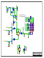
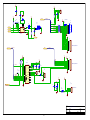
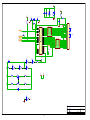
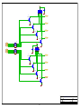
1
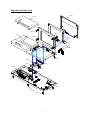
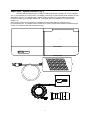
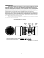
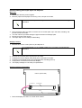
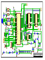
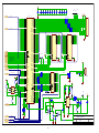
Super Spiro - Service Manual
056-09 Issue. 1.0
November 1999
Contents
Exploded isometric view
Parts list
System overview
Transducer
Disassembly instructions
Re-assembly instructions
Circuit description
Microprocessor circuit
Flash disk
Serial interface
Transducer interface
Frame store
FPGA
Keypad circuit
Real time clock circuit
Sound generator circuit
Printer control circuit
Expansion
Printer driver circuit
Technical support
Fault analysis
Circuit diagrams
Micro processor circuit
FPGA circuit
Keypad circuit
Real time clock circuit
Printer circuit
Printer driver 1
Printer driver 2
Page 3
Page 4
Page 5
Page 6
Page 7
Page 8
Page 9
Page 9
Page 10
Page 10
Page 10
Page 10
Page 11
Page 11
Page 12
Page 12
Page 12
Page 12
Page 12
Page 13
Page 14
Page 15
Page 16
Page 17
Page 18
Page 19
Page 20
Page 21
2
Exploded Isometric View
Item 8
Item 10
Item 15
Item 20
Item 1
Item 16
Item 21
Item 7
Item 4
Item 9
Item 18
Item 6
Item 17
Item 12
Item 14
Item 22
Item 9
Item 13
Item 11
Item 2
Item 23
Item 5
Item 3
Item 19
3
Parts List
ITEM No.
1
2
3
4
5
6
7
8
9
10
11
12
13
14
15
16
17
18
19
20
21
22
23
DESCRIPTION
TOP MOULDING
BACK PANEL
SIDE PANEL
DISPLAY CABLE ASSEMBLY
BOTTOM MOULDING
HINGE BLOCK
DISPLAY FRONT
DISPLAY BACK
DISPLAY HINGE ASSEMBLY
PAPER COVER
CSK SELF TAPPING SCREW 9mm LONG
SPEAKER
SPEAKER COVER
CONTRAST WHEEL
SCREW COVER
CSK SELF TAPPING SCREW 8mm LONG
CSK SELF TAPPING SCREW 13mm LONG
M3 MACHINE SCREW 6mm LONG
CSK SELF TAPPING SCREW 18mm LONG
DISPLAY LATCH
DISPLAY LATCH BUTTON
PRINTER MECHANISM
THERMAL PRINT HEAD
4
MICRO MEDICAL PT No.
MLD5611A
MLD5615C
MLD5615B
ASS5624
MLD5612A
MLD5618
MLD5613
MLD5614
ASS5601
MLD5617
SCR5604
SPKR100
MLD5620
MLD5621
MLD5616
SCR5602
SCR5601
SCR0306
SCR4700
MLD5619
MLD5622
PTR4200
TPH3000
Super Spiro - System Overview (Fig. 1)
The Micro Medical Super Spiro is a data recording spirometer consisting of a microcomputer
unit (1) incorporating a 1/4VGA colour LCD display, data entry keypad, RS232 serial interface and all
associated circuitry. It is supplied with a digital volume transducer (2), disposable mouthpieces,
transducer holder (3) and mains adapter (4). The Super Spiro is powered by a universal mains
adapter (4).
When testing a subject the transducer is inserted into the holder which is plugged into the
microcomputer unit. The digital volume transducer is used to measure the subjects expired flow and
volume in accordance with the operating manual.
1
su p e r
spiro
4
Micro
Medical
3
2
5
Transducer (Fig. 2)
The Micro Medical digital volume transducer consists of an acrylic tube with a vane positioned
between two swirl plates. The low inertia vane is attached to a stainless steel pivot, which is free to
rotate on two jewelled bearings mounted at the centre of the swirl plates. As air is passed through the
transducer the swirl plates create a vortex, which causes the vane to rotate in a direction dependant
upon the direction of airflow. The number of rotations is proportional to the volume of air passed
through the transducer and the frequency of rotation is proportional to the flow rate. The transducer
housing consists of a main body that contains a pair of light emitting diodes (LED’s) and
phototransistors. The transducer is fixed to the mouthpiece holder which pushes into the main body
and is captured by an “O” ring seal. The LED’s produce infra red beams which are interrupted by the
vane twice per revolution. This interruption is sensed by the phototransistors. The output from the
collector of each phototransistor will be a square wave with a phase difference between the two of +
or - 90 degrees depending upon the direction of flow.
There is no routine maintenance required for the transducer other than cleaning according to
the instructions in the operating manual.
Micro Medical Digital Volume Transducer
Rotating
vane
Infra red
emitter
Swirl
plate
Jewelled
bearing
Infra red
detector
Volume = k X No. of pulses
Volume proportional to the number of pulses
Flow proportional to the puse frequency
Flow = k / pulse period
6
Disassembling the Super Spiro for Repairs
Main Unit
1. Disconnect all mains power supplies
2. Remove paper roll and paper roll housing cover, and put to one side
We recommend that you use a Philip Number Zero screwdriver for the following
instruction.
3. Place the Super Spiro face down to remove the six screws (Item 19) in the lower moulding, and
put the screws to one side.
4. Turn the unit face up before easing the upper and lower mouldings apart.
5. Reconnect mains power supply
6. The Super Spiro is now ready for fault finding.
Display Console
1. Remove the 4 screw covers (item 15) and dispose of.
We recommend that you use a Philip Number Zero screwdriver for the following
instruction.
2.
3.
4.
5.
6.
Remove the 4 screws (item 16) and put to one side.
Carefully remove the display front panel (item 7) and put to one side.
Carefully pull the display away from the display back moulding (item 8).
Unplug the 2 connectors from the main display.
The display backlight is now ready for replacement.
Display backlight replacement
DISPLAY (REAR VIEW)
CFL CONNECTOR
INVERTOR BOARD
CFL UNIT
FIXING SCREW
KCS3224A CFL UNIT
1. Place the display face down on a clean work surface
7
2. Unplug the connector from the Invertor board situated on the back of the display.
We recommend that you use a Philip Number Zero screwdriver for the following
instruction.
3. Loosen the fixing screw located on the CFL unit.
4. Slide the CFL unit to the opposite direction to the arrow mark (located on the CFL unit) and pull
the unit gently up.
5. Safely dispose of the CFL unit.
6. Take a new CFL unit and position in the original place.
7. Slide the CFL unit in the direction of the arrow.
8. Tighten the fixing screw to secure the CFL unit.
9. Reconnect the connector on the CFL unit to the invertor board.
Reassembling the Superspiro after repairs
Main unit
1. Disconnect all mains power supplies
2. Position the top moulding over the bottom moulding and ensure that they both mate ensuring that
the contrast wheel (item 14) is correctly located.
3. Place the Super Spiro face down and insert the six screws.
4. Turn the unit face up and connect the mains supply.
5. Turn the unit and offer up the paper roll as explained in the operating manual.
6. Replace the paper cover.
7. The Super Spiro is now ready for operation.
Display console
1.
2.
3.
4.
5.
Reconnect the 2 connectors on item 4 to the plugs on the display ensuring correct polarity.
Position the display over the locating pillars on the display back panel (item 8).
Position the display front panel (item 7) over the display.
Secure the display using 4 screws (item 16)
Replace the 4 screw covers (item 15).
8
Circuit Description
The Super Spiro board was designed primarily to interface with the Micro Medical Spirometer turbine,
but the interface was kept open ended so that other modules, for example, airways resistance by the
interrupter method (Rint) can be attached. Furthermore, a 9 pin ‘D’ type connector was also designed
in to allow other ‘customer special’ modules to be attached. Provision was given to add a mezzanine
board for customer special interface circuitry to be connected.
The main features of the design are:
Intel 80386EX micro controller.
2 Mbytes of DRAM (only 1 Meg is used).
512 Mbytes of Flash EPROM for programme. (256K used)
2 Mbytes of Flash EPROM as Flash disk memory.
Dual frame store of 320 X 240 X 8 pixels.
Second frame store can be scrolled horizontally or vertically.
Frame store, key pad, Dram etc. are all controlled by single FPGA chip.
Boot software can be downloaded using the JTAG port.
In built printer and printer controller.
Serial port for external PC communication / external printer.
RJ11 interface to Micro Medical modules.
The following paragraphs describe the circuits printed at the end of this manual. Signal and
component names shown on the circuit diagrams are printed in bold type.
Microprocessor circuit (Drawing 056-02)
The board is controlled by an Intel 80386EX, U14, running at 25 MHz. The crystal oscillator, U15, of
50MHz drives the processor, as twice the operating frequency is required. U10 (MAX 824) controls
the reset of the processor, such that it resets the processor if the supply voltage drops below 4.6V.
The processor requires a high active reset line whilst the rest of the board requires a low active reset.
The start up program is stored in U20, a 512 Mbytes Flash EEPROM – TE28F160S. This is selected
by the signal UCS (U14 pin 1) which is always active on start up. The reset of the chip select lines
are then programmed by the boot routine.
The program memory has two major parts, the boot section and non-boot section. The boot section is
secured, and can only be programmed if the link LK1 is present and VPPEN (U14 pin 110) is
enabled, supplying VCC to pin 13 of U19. This section is programmed with a boot loader via the onboard socket, J9. Whilst this is happening the processor goes into suspend mode, and all its pins are
then available in a long shift register. By entering a correct sequence of code, via J9, the boot loader
can be programmed into U19. Once this is done, the link is removed and processor is reset and it
would then run the boot loader, thus allowing further software to be downloaded. The rest of U19 is
filled with kernel software that controls the flash disk as well as most I/O functions, just as the BIOS
does in the PC.
U18 is 1M X 16 (2 Mbytes) DRAM which is the main RAM of the processor. Only 640 K is directly
available to the processor, and 128 K is used for storing the display image temporarily (see later).
The DRAM refresh and address multiplexing is controlled by U13 – Xilinx XC4006E FPGA. The chip
select for the DRAM, UC3, is mapped for 0 - $BFFFF, but $A0000 - $BFFFF is frame store memory,
so UC3 is only valid if frame store is invalid. This will become clearer in the Frame Store section.
Q23, Q24 and U22A are used to switch on 5 volts to VPP of Flash EEPROM. This gives extra
security against any part of the program becoming corrupted by software. However, the software can
write the non-boot section, by enabling the VPP line and following the EEPOM erase/write algorithm.
Chances of both these events accidentally happening are very small. Nevertheless, the boot software
is completely protected by the absence of Link LK1.
9
Flash Disk (Drawing 056-02)
The flash disk, U20, behaves just like a PC floppy disk drive except that it is non-removable. Its size
is 2 Mbytes with sector size of 512 bytes. The main difference is that there is a finite number
(approximately 100,000) of times the sectors can be written, so an intelligent disk operating system is
employed to rotate the sectors round, and delete the others when no system activity is envisaged.
Delete takes few milliseconds. The Flash Disk is mapped at $C8000 - $CBFFF (16K blocks). There
are 128 pages of 16K, and the pages are controlled by 8 bit latch U17, which holds the page number
(higher addresses) of the Flash disk.
The board is designed to accommodate a larger 4 Mbytes device with 256 pages.
The MSB of the page line (U17/19) is connected to green led. This is mainly used for testing of the
board and has no other significance.
Serial Interface (Drawing 056-02)
U4 (MAX3223) converts logic levels to RS232 levels. J3, a 9-pin female D type connector, is used as
the external RS232 port. The signal pins are such that it can make one to one connection with the PC
serial port. It has the facility to use hardware handshaking lines CTS and RTS, but these are currently
not used. If power supply is required from the RS232 connection, say to drive a serial to parallel
converter, then fuse FS2 can be fitted to give 5V on pin 4
J3 pin connections.
1
2
3
4
5
6
7
8
9
N/C
TX
RX
5V*
GND
N/C
CTS
RTS
N/C
* If fuse connected.
Transducer Interface (Drawing 056-02)
The connector, J13, is used for connecting to Micro Medical transducers, namely Spirometer turbine,
Rint and NEP transducers. It is a 6-pin interface, though for turbine, the middle 4 lines are used. 12V
power is available on pin 5 and GND on pin 4. The rest of pins are multifunction, and can be
configured in various ways, either as inputs, outputs or SPI bus. Pins 2 and 3 have schmitt trigger
inputs connected to it, mainly for turbine operation.
Frame Store (Drawing 056-03)
Frame Stores are mapped from address $A0000 to $BFFFF (128 Kbytes). Although, the actual
display is 320 X 240 pixels, the frame store is organised as 512 X 256 pixels. This organisation
makes the design much simpler. The frame store memory U11 and U12 are both high speed static
RAM, U11 being a fixed frame store (A) and U12 a scrolling frame store (B). They overlay on top of
each other and their mode can be controlled by I/O register in the FPGA, U13. It can be organised as
A on B, B on A, A only or B only. A on B means that where the A data is 0, B data is displayed. This
allows a border to be displayed on fixed screen, and a waveform scrolled inside the window.
During read, both the memories are multiplexed, so that its data can be read in one cycle. The
display requires data as 8 bits, with r1, g1, b1, r2, g2, b2, r3, g3 as the first byte, b3, r4, g4, b4, r5, b5,
g5, r5 as the second byte and so on. The data from frame store is available as pixel 1, pixel 2 etc.
with each pixel being 8 bits. The FPGA has the necessary look up table to display 64 colours (bits 0 –
10
bits 5) and converts pixel data to RGB data as required by LCD. This is a complex operation and is
beyond the scope of this document. It is sufficient to know that the RGB data is sent out to LCD via
J11.
DISP_FRAME signal is a single line, active low pulse at the start of every frame.
DISP_LOAD is a single, active low, clock pulse at the start of every line.
DISP_CLK clocks the data DISP_D0 – DISP_D7 into the display.
DISP_CNTL enables the display.
U25 is a DC to DC converter to give 26.4 volts from 5V supply. This is the bias voltage for the LCD
display. It can be slightly adjusted by VR1 to give better contrast at different viewing angles.
J10 is a back light connector that provides power to the back light. Q22 is used to enable the back
light. It was designed for power saving, but since the unit only operates on mains, this feature is not
currently used. VR3 controls the back light intensity in some back light modules, but this feature is not
in the modules currently fitted.
The frame store data can be saved quickly in the RAM that resides in the same address space, using
a block transfer. This is done by first programming the CS3 line to address space $A0000 - $AFFFF.
Since $B0000 - $BFFFF is now not the part of CS3, the FPGA will map it to DRAM. The whole 64K
page can be transferred from $A0000 (frame store) to $B0000 (RAM). The CS3 line is then
programmed for $B0000 - $BFFFF allowing $B0000 (frame store) page to be transferred to $A0000
(RAM) page. CS3 is then restored back to $A0000 - $BFFFF.
Restoring the screen is inverse of the above procedure.
FPGA (Drawing 056-03)
This device controls most of the circuitry not controlled by the processor. The program for the FPGA
resides in serial EEPROM, U8, and is downloaded once on power up. The processor monitors the
FPGADONE line to ensure that FPGA is programmed before commencing, otherwise, the DRAM will
not be operational.
Besides DRAM, the FPGA controls the LCD display, keypad, sound chip, and most of chip select
lines. These CS lines can be programmed in the processor, but this can be further qualified in the
FPGA if necessary. There are some spare serial enable lines for an additional 9 pin I/O port and the
mezzanine expansion board.
Keypad Circuit (Drawing 056-04)
The keypad consists of a matrix of 25 keys together with a separate paper feed key and on/off key.
The matrix is read by successively pulling the columns of the matrix low, KEYOUT[0..4], and reading
the state of the rows, KEYIN[0..4], to determine which key has been pressed. KEYOUT[0..4] and
KEYIN[0..4] are connected directly to the FPGA (see 056-03). The diodes, D7and D8, prevent
current flowing between the lines of KEYOUT[0..4] in the event of two keys on the same row being
depressed simultaneously. The resistor network, RN5, bias KEYIN[0..4] to VCC.
The on/off switch is used to apply the 5V from the external power supply to the circuit, VCC, and
turning the unit on. When the on/off key is depressed, the pull up resistor, R3, is pulled to ground.
R3, C17 and the schmitt input gate U3A form a de-bounce circuit whose output is applied to the clock
input of a bi-stable latch, U2B, that is powered directly from 5V and is active all the time the power
supply is plugged in. The output of the latch is applied to Q19 that in turn switches the series pass
transistor, Q20, to connect 5V to VCC. The latch, U2B, is also controlled by the set and reset inputs.
By taking the set input to 5V the unit will be turned on and by taking the reset input to 5V the unit will
be turned off regardless of the clock input. The set input is asserted by either the real time clock
alarm output, RTC_INT (see 056-05), or by the POWER_ON signal from the processor (see 056-02).
The reset input is asserted or by the POWER_OFF signal from the processor.
11
Real Time Clock Circuit (Drawing 056-05)
The real time clock, U16, is set by the processor during the factory set-up and may be adjusted using
the configuration module. The processor communicates with the real time clock through a bidirectional serial interface line, RCA_DATA, is clocked by RTS_CLK, and is selected by RTC_SEL.
The processor (see 056-02) generates these three control lines.
Sound Generator Circuit (Drawing 056-05)
The various sounds used in the spirometry tests are generated by U7 and associated components.
This device contains the addressable, pre-programmed sounds and is controlled by the lines,
SNDCNT[0..5], generated by the FPGA (see 056-03).
Printer Control Circuit (Drawing 056-06)
The printer driver uses a single chip micro-controller, U6, with on board program memory and RAM to
receive serial data from the microprocessor, U14, and control the printer mechanism. The
asynchronous serial lines PRNTDATA and PRNTACK are used by U14 to send and receive data to
and from U6. The signal BUSY generated by U6 is used to control the flow of data from U14 and PF
is generated by the paper feed key.
The printer mechanism uses stepper motors to drive the print head and paper feed. Each stepper
motor uses four lines, driven sequentially. The order in which the lines are driven determines the
direction of rotation. The thermal print head uses eight heater elements. The stepper motors and
print head signals are generated on port A and B (active high) of U6. Timing for Port A and B is
derived from an adjustable oscillator comprising of U9 and associated components. Adjusting VR2
varies the oscillator frequency and consequently the period for which the thermal elements are
energised. This in turn adjusts the print density. After the micro-controller is first reset, the print head
is driven to the left until the end switch is activated. The end switch consists of a normally closed pair
of contacts accessed at pins 1 and 2 of the printer connector J2. The end switch is detected by PD5
on the micro-controller.
Expansion (Drawing 056-05)
J8 and J12 are 10-pin header connectors that allow a mezzanine card to be fitted. This is used for
future customer special circuitry. Similarly, J14 is placed near the output plate on the right side of the
unit to allow customer special signals to be connected to the mezzanine board or to the processor
directly.
Printer Driver Circuits (Drawings 056-07 and 056-08)
The outputs from port A and B of U6 drives the two stepper motors and eight thermal elements
through the high current transistors Q1 to Q16 in common emitter configuration. Diodes D1 to D4 are
used to dissipate the inductive fly-back from the stepper motors and elements.
Power Supply
An external, dual voltage, supply provides 5.5 volts and 12 volts to socket J1 (Drawing 056-05). This
power supply has a universal input, is factory sealed, and contains no user serviceable parts.
12
Technical Support
Great Britain and World Headquarters
Micro Medical Ltd
PO Box 6
Rochester
Kent ME1 2AZ
Telephone
+ 44 (0)1634 360044
Fax
+44 (0)1634 360055
Web Site
http://www.micromedical.com.uk
Email
[email protected]
Contact Micro Medical Ltd for the local agent in your region or country for local service:
13
Fault Analysis
The following analysis is only a guideline and should be carried out in a logical sequence. If the fault
is still apparent after the following suggestions then the unit should be fault found using the circuit
descriptions and circuit diagrams provided.
When the unit is turned on there is no display present
-Ensure charger is turned on at the mains.
FVC readings are low
-Remove turbine from transducer housing. Taking the turbine, move it slowly through the air and
check that the vane is not sticking.
The unit does not record any blows
-Inspect transducer housing connector for damage.
-Check that transducer housing lead is properly connected to the RJ11 socket.
-Remove turbine from transducer housing. Taking the turbine, move it slowly through the air and
check that the vane is not sticking.
-Blow into transducer housing and move transducer head cable around to check for breaks in the
cable.
14
UADS
UWR
URD
VCC
VCC
U10
5
VCC
4
C41
0.1UF
3
RES
RESET-
R33
10K
VCC
D[0..15]
WDI
2
GND
1
RES
D[0..15]
A[1..21]
A[1..21]
MAX824_EUKM
VCC
U14
GND
1
EN
UREADY
50MHz
TP1
VCC TX
N
98
79
RX TP2
U4
J3
16
9
1
6
2
7
3
8
4
9
5
R1 IN
R2 IN
RS232
T1 OUT
T2 OUT
17
8
1
C26
0.1UF
R1 OUT
R2 OUT
TTL
T1 IN
T2 IN
EN
14
DB9
VPPEN
2
4
3
INVALID
FON
FOFF
C1+
C1 V+
C2+
C2 V-
15
10
13
12
11
20
CS0
C24 0.1UF
UCS1
UCS2
UCS3
5
6
7
MAX3223CAP
C25
0.1UF
12V
VCC
C23
0.1UF
TP21
TURB1
U22B
R49
3K3
R48
3K3
3
ONLINE
PRNBUSY
4
SN74HC14 SND_EOM
RTC_INT-
J13
U22C
1
2
3
4
5
6
5
6
C72
1nF
TURB2
128
122
127
139
123
UCS5
INT1
INT2
DRQ1/RXD1
DACK1#/TXD1
DRQ0/DCD1#
DACK0#/CS5#
EOP#/CTS1#
106
84
86
85
STXCLK
SSIOTX
SSIORX
R20
PRNTACK
PRNTDATA
1
2
3
4
5
6
7
8
9
10
VCC
J7
1
2
3
4
MOLEX 4PIN
DSR1#/STXCLK
DTR1#/SRXCLK
RTS1#/SSIOTX
RI1#/SSIORX
82
27
28
129
107
J9
0R
D0
D1
D2
D3
D4
D5
D6
D7
D8
D9
D10
D11
D12
D13
D14
D15
BUSY#/TMRGATE2
PEREQ/TMRCLK2
ERROR#/TMROUT2
SN74HC14
1nF
RJ11
INT4/TMRCLK0
INT5/TMRGATE0
INT6/TMRCLK1
INT7/TMRGATE1
100
96
99
TP25
C71
P3.0/TMROUT0
P3.1/TMROUT1
P3.2/INT0
P3.3/INT1
P3.4/INT2
P3.5/INT3
P3.6/PWRDOWN
P3.7/COMCLK
101
102
103
104
0R
R8
P2.0/CS0#
P2.1/CS1#
P2.2/CS2#
P2.3/CS3#
P2.4/CS4#
P2.5/RXD0
P2.6/TXD0
P2.7/CTS0#
80
81
87
89
91
92
93
94
VCC
A1
A2
A3
A4
A5
A6
A7
A8
A9
A10
A11
A12
A13
A14
A15
A16
A17
A18
A19
A20
A21
A22
A23
A24
A25
SMIACT
BHE
BLE
P1.0/DCD0#
P1.1/RTS0#
P1.2/DTR0#
P1.3/DSR0#
P1.4/RI0#
P1.5/LOCK#
P1.6/HOLD
P1.7/HLDA
133
134
135
136
137
140
142
143
CS4
ADS
W/R
D/C
M/IO
RD
WR
LBA
NMI
SMI#
110
111
113
114
115
116
117
121
PWR_OFFPWR_ONRTC_SELRTC_CLK
RTC_DATA
FPGADONE
U20
RESET
CLK2
NA#
BS8#
READY
TCK
TDI
TMS
TRST#
FLT#
UCS
CS6#/REFRESH#
WDTOUT
TDO
CLKOUT
43
32
31
29
37
38
4
A1
A2
A3
A4
A5
A6
A7
A8
A9
A10
A11
A12
A13
A14
A15
A16
A17
A18
A19
A20
A21
45
46
48
49
52
53
54
55
56
57
58
59
61
62
63
64
66
67
68
70
71
73
74
76
78
130
42
40
5
6
7
8
10
12
13
14
15
17
19
20
21
22
23
25
TP11
CS0
A1
A2
A3
A4
A5
A6
A7
A8
A9
A10
A11
A12
A13
FA14
FA15
FA16
FA17
FA18
FA19
FA20
FA21
CS0
32
28
27
26
25
24
23
22
20
19
18
17
13
12
11
10
8
7
6
5
4
3
A0
A1
A2
A3
A4
A5
A6
A7
A8
A9
A10
A11
A12
A13
A14
A15
A16
A17
A18
A19
A20
A21
14
2
54
55
15
CE0
CE1
OE
WE
VPP
VCC
D0
D1
D2
D3
D4
D5
D6
D7
D8
D9
D10
D11
D12
D13
D14
D15
33
35
38
40
44
46
49
51
D0
D1
D2
D3
D4
D5
D6
D7
34
36
39
41
45
47
50
52
D8
D9
D10
D11
D12
D13
D14
D15
U19
A1
A2
A3
A4
A5
A6
A7
A8
A9
A10
A11
A12
A13
A14
A15
A16
A17
A18
A19
VCC
BYTE
STS
RP
WP
NC
NC
31
53
16
56
25
24
23
22
21
20
19
18
8
7
6
5
4
3
2
1
48
17
16
UCS
26
28
11
13
RESET-
29
30
A0
A1
A2
A3
A4
A5
A6
A7
A8
A9
A10
A11
A12
A13
A14
A15
A16
A17
A18
D0
D1
D2
D3
D4
D5
D6
D7
D8
D9
D10
D11
D12
D13
D14
D15
D0
D1
D2
D3
D4
D5
D6
D7
30
32
34
36
39
41
43
45
D8
D9
D10
D11
D12
D13
D14
D15
VCC
47
BYTE
CE
OE
WE
VPP
29
31
33
35
38
40
42
44
LK1
12
14
RP
WP
1
2
LINK2
L
i
28F400B5T80
R37
10K
TE28F320J5100
URD
UWR
UCS0
UBHE
UBLE
D0
D1
D2
D3
D4
D5
D6
D7
D8
D9
D10
D11
D12
D13
D14
D15
TP15
CS4
U22D
LED1
9
8
1
TP20
UCS
CS4
1
11
D0
D1
D2
D3
D4
D5
D6
D7
3
4
7
8
13
14
17
18
VCC
3
U17
R52
2
GREEN
G
CLK
1Q
2Q
3Q
4Q
5Q
6Q
7Q
8Q
1D
2D
3D
4D
5D
6D
7D
8D
2
5
6
9
12
15
16
19
FA14
FA15
FA16
FA17
FA18
FA19
FA20
FA21
470R
SN74HC14
VCC
UUCS
2
2
119
125
44
35
34
3
CLK
TP16
VPP_EN
R36
Q23
FMMT549
1
100R
74FCT377
1
2
124
1
REFRESH
R50
112
VPPEN
R29
VCC
FA80386EX25L
Q24
VCC
26
1
C63
2
R35
10K
CLK25MHZ
33R
DTC114EKA
U22A
100K
3
FS2
300mA
C51
1UF
VCC
3
10R
4
2
U15
R30
0.1UF
C62
1UF
SN74HC14
VCC
VCC
5V
TP4
GND
HEADER 5X2
TP28
GND
TP3
GND
TP24
GND
VCC
R53
470R
S
D9
5.6V
VCC
C4
0.1UF
R54
10K
3
10
C47
0.1UF
C45
0.1UF
C66
0.1UF
C74
0.1UF
C58
0.1UF
C21
0.1UF
C52
0.1UF
C61
0.1UF
C50
0.1UF
C60
0.1UF
LED2
GREEN
RED
B
C46
0.1UF
11
2
470R
SN74HC14
U22E
LED3
1
1
R51
2
VCC
12
SN74HC14
Title
P
Super Spiro - Processor circuit
VSS
Size
3
U22F
13
A3
Date:
File:
15
Number
Revision
056-02
5-Oct-1999
G:\tempd\056-02.sch
Sheet of
Drawn By:
1.0
VCC
TP27
C42
C53
C43
C48
C39
C38
C67
C31
C68
0.1UF
0.1UF
0.1UF
0.1UF
0.1UF
0.1UF
0.1UF
0.1UF
0.1UF
0.1UF
KEYIN0
KEYIN1
KEYIN2
KEYIN3
KEYIN4
KEYOUT[0..4]
KEYOUT[0..4]
113
109
112
111
115
VCC
KEYIN0
KEYIN1
KEYIN2
KEYIN3
KEYIN4
VCC
VCC
R34
R26
100K
R21
10K
100K
KEYOUT0
KEYOUT1
KEYOUT2
KEYOUT3
KEYOUT4
U8
17
14
6
VP
D
CEO
CLK
RES
CE
XC17512L
105
106
107
108
114
82
117
119
80
59
2
4
8
EXP2
EXP3
EXP4
6
121
7
13
VCC
40
38
42
R22
100K
KEYOUT0
KEYOUT1
KEYOUT2
KEYOUT3
KEYOUT4
PROGRAM
DIN
CCLK
DONE
INIT
TDI
TDO
TCK
TMS
M0
M1
M2
MEMB_CS
MEMB_OE
MEMB_WE
DRA0
DRA1
DRA2
DRA3
DRA4
DRA5
DRA6
DRA7
DRA8
DRA9
DRRAS
DRCASU
DRCASL
DROE
DRWE
SEREN0
SEREN1
SEREN2
SEREN3
SEREN4
SNDCNTL0
SNDCNTL1
SNDCNTL2
SNDCNTL3
SNDCNTL4
SNDCNTL5
52
53
54
55
5
6
7
8
1
2
3
4
8
7
6
5
33R
33R
33R
33R
RN6D
83
77
75
73
71
68
66
64
67
69
76
72
62
65
58
57
56
MEM_A0
MEM_A1
MEM_A2
MEM_A3
MEM_A4
MEM_A5
MEM_A6
MEM_A7
MEM_A8
MEM_A9
MEM_A10
MEM_A11
MEM_A12
MEM_A13
MEM_A14
MEM_A15
MEM_A16
85
87
89
92
90
88
86
84
MEM_D0
MEM_D1
MEM_D2
MEM_D3
MEM_D4
MEM_D5
MEM_D6
MEM_D7
U11
MEM_A0
MEM_A1
MEM_A2
MEM_A3
MEM_A4
MEM_A5
MEM_A6
MEM_A7
MEM_A8
MEM_A9
MEM_A10
MEM_A11
MEM_A12
MEM_A13
MEM_A14
MEM_A15
MEM_A16
12
11
10
9
8
7
6
5
27
26
23
25
4
28
3
31
2
A0
A1
A2
A3
A4
A5
A6
A7
A8
A9
A10
A11
A12
A13
A14
A15
A16
VCC
TP9
TP10
U12
24
29
30
22
MEM_D0
MEM_D1
MEM_D2
MEM_D3
MEM_D4
MEM_D5
MEM_D6
MEM_D7
13
14
15
17
18
19
20
21
D0
D1
D2
D3
D4
D5
D6
D7
MEM_A0
MEM_A1
MEM_A2
MEM_A3
MEM_A4
MEM_A5
MEM_A6
MEM_A7
MEM_A8
MEM_A9
MEM_A10
MEM_A11
MEM_A12
MEM_A13
MEM_A14
MEM_A15
MEM_A16
VCC
OE
WE
CS2
CS1
12
11
10
9
8
7
6
5
27
26
23
25
4
28
3
31
2
A0
A1
A2
A3
A4
A5
A6
A7
A8
A9
A10
A11
A12
A13
A14
A15
A16
24
29
30
22
1
NC
KM681000BLG-7
OE
WE
CS2
CS1
MEM_D0
MEM_D1
MEM_D2
MEM_D3
MEM_D4
MEM_D5
MEM_D6
MEM_D7
13
14
15
17
18
19
20
21
D0
D1
D2
D3
D4
D5
D6
D7
CON15
1
NC
KM681000BLG-7
VCC
78
74
63
J10
95
94
93
U18
22
21
18
17
4
5
8
9
11
12
23
15
16
14
24
37
36
35
34
104
102
96
99
97
98
103
4
4
3
2
1
4
3
1
2
33R
33R
33R
33R
33R
33R
33R
33R
SEREN0
SEREN1
SEREN2
SEREN3
SEREN4
SNDCNTL0
SNDCNTL1
SNDCNTL2
SNDCNTL3
SNDCNTL4
SNDCNTL5
1
2
3
5
6
7
8
33R
33R
33R
33R
5
18
19
20
21
24
25
26
27
28
29
8
7
6
5
6
3
8
4
7
2
1
6
33R
33R
33R
33R
A0
A1
A2
A3
A4
A5
A6
A7
A8
A9
15
31
32
30
14
5
7
8
RAS
D0
D1
D2
D3
D4
D5
D6
D7
D8
D9
D10
D11
D12
D13
D14
D15
RAS
UCAS
LCAS
OE
WE
LCAS
2
3
4
5
7
8
9
10
UD0
UD1
UD2
UD3
UD4
UD5
UD6
UD7
35
36
37
38
40
41
42
43
UD8
UD9
UD10
UD11
UD12
UD13
UD14
UD15
1
BKLGTEN
1
Q22
1
2
3
4
5
3
VR3
DTC114EKA
B_5B-ZR
10K
Back Light Connector
VCC
C65
0.1UF
+ C64
L1
47UH
TP22
KM416C1200BT-6
TP19 TP18 TP17
VEE
VEE
U21
VCC
1
C33
5
3
0.1UF
EXP0
FPGADONE
15
14
13
12
11
10
9
8
7
6
5
4
3
2
1
2
KEYIN[0..4]
33R
33R
33R
33R
D11
1
KEYIN[0..4]
INT1
INT2
CLK25MHZ
MEMA_CS
MEMA_OE
MEMA_WE
4
3
2
1
J11
3
INT1
INT2
CLK25MHZ
MEM_D0
MEM_D1
MEM_D2
MEM_D3
MEM_D4
MEM_D5
MEM_D6
MEM_D7
5RN7D
6
7
8
VEE
2
123
116
124
MEM_A0
MEM_A1
MEM_A2
MEM_A3
MEM_A4
MEM_A5
MEM_A6
MEM_A7
MEM_A8
MEM_A9
MEM_A10
MEM_A11
MEM_A12
MEM_A13
MEM_A14
MEM_A15
MEM_A16
33R
33R
33R
33R
47UF/10V
Flash Disk C8000 - CBFFF
Display A0000 - BFFFF
Display Reg (I/O) 200 - 20F
DRAM 00000 - DFFFF
SPARE
UBHE
UBLE
UWR
URD
READY
REFRESH
CS1
CS2
CS3
CS4
CS5
DISP_CNTL
DISP_CLK
DISP_LOAD
DISP_FRAME
RN8D
4
3
2
1
43
44
45
46
47
48
49
50
VCC
8
155
156
157
158
159
2
125
126
127
128
129
UA1
UA2
UA3
UA4
UA5
UA6
UA7
UA8
UA9
UA10
UA11
UA12
UA13
UA14
UA15
UA16
UA17
UA18
UA19
UA20
DISP_D0
DISP_D1
DISP_D2
DISP_D3
DISP_D4
DISP_D5
DISP_D6
DISP_D7
UCAS
154
153
152
150
149
148
147
146
145
144
143
140
139
138
137
135
134
133
132
130
UD0
UD1
UD2
UD3
UD4
UD5
UD6
UD7
MEMB_SEL
UBHE
UBLE
UWR
URD
UREADY
REFRESH
UCS0
UCS1
UCS2
UCS3
UCS5
UA1
UA2
UA3
UA4
UA5
UA6
UA7
UA8
UA9
UA10
UA11
UA12
UA13
UA14
UA15
UA16
UA17
UA18
UA19
UA20
33
32
31
30
28
27
26
25
MEMA_SEL
UA[1..21]
UA[1..21]
DISP_CNTL
XC4006E-3PQ160C_VIDEO
UD0
UD1
UD2
UD3
UD4
UD5
UD6
UD7
TP26
DISP_FRAME
C49
0.1UF
DISP_CLK
C59
0.1UF
DISP_LD
C44
0.1UF
U13
UD[0..15]
UD[0..15]
TP29
TP23
C69
2
SHDN
LX
26.4V
1
7
3
2
ISET
ZHCS750
R39
REF
C75
680K
POL
FB
C70
+
100pF
4
C73
0.1UF
22UF/35V
2
3
1
EXP1
2
3
1
U5B
6
-
4
7
6
8
VR1
EXP[0..4]
36K
0.1UF
+
LM2904D
EXP[0..4]
R40
6
Contrast
U5A
C34
-
4K7
1
4K7
4K7
8
MAX629ESA
RN9C
5
100K
LM2904D
7
+
Title
C28
SEREN[0..4]
SNDCNTL[0..5]
3
SNDCNTL[0..5]
R38
0.1UF
SEREN[0..4]
1M0
Size
A3
Date:
File:
16
Super Spiro - FPGA circuit
Number
Revision
056-03
5-Oct-1999
G:\tempd\056-03.sch
Sheet of
Drawn By:
1.1
A
l
t
VCC
5V
FS3
8
1
1A
+ C3
47UF/16V
C19
0.1UF
RL1
4
D5
7
2
+ C57
47UF/16V
5
MINIRELAY (RS345-022)
2
3
1
ZHCS750
Q20
FMMT717
2
3
KEYOUT[0..4]
KEYOUT[0..4]
D7
+ C27
1
47UF/16V
KEYIN[0..4]
KEYIN[0..4]
C22
0.1UF
1
KEYOUT0
5
2
KEYOUT1
4
3
D8
KEYOUT2
6
1
KEYOUT3
5
2
IMN10
3
R11
100R
6
DTC114EKA
KEYOUT4
Q19
4
3
1
2
R5
100K
R6
3
10
4093
Q18
FMMT489
1
100K
8
5
3
RN5C
2
RN5B
8
13
Q
D
U2B
9
Q
10
1
3
1
2
esc
F1
del
F2
7
4
1
F3
0
8
5
2
F4
.
9
6
3
F5
ON/OFF
PAPER
FEED
13
2
4093
R
12
100K
7
6
100K
12
U3A
11
CLK
5V
100K
6
7
R3
100K
S
C20
0.1UF
RN5A
R16
KEYIN4
8K2
R10
2K0
1
KEYIN3
9
2
PWR_ON-
R12
100K
5
8
KEYIN2
5V
U3C
8
OR
RN5D
KEYIN1
N
RTC_INT-
4
KEYIN0
3
VCC
4
5V
9
IMN10
C17
0.1UF
PAPERFEED-
11
J6
KEYPAD
10
4013
R4
100K
U3B
5
3
4
R9
1
4093
8K2
5V
14
6
S
VCC
Q
U2A
1
12
C15
0.1UF
U3D
11
CLK
13
Q
2
4093
7
R
3
D
GND
C16
0.1UF
5
14
5V
4013
4
C18
0.1UF
7
R7
2K0
2
PWR_OFF-
6
Q17
FMMT489
Title
Size
Super Spiro - Keypad circuit
Number
A3
17
Date:
File:
5-Oct-1999
G:\tempd\056-04.sch
Revision
056-04
Sheet of
Drawn By:
1.0
VCC
VCC
U1
3
2
1
C56
0.1UF
C54
33PF
C8
0.1UF
R2
10K
VCC
VDD
DQ
GND
DS1821
VCC
X2
Resettable Fuse
VCC
J14
5
RTC_DATA
FS4
300mA
SEREN4
1
SCL
OSCI
A0
SDA
2
8
VDD
INT
1
2
STXCLK
SEREN1
SSIOTX
SEREN2
4
VSS
3
BAV70
7
R32
10K
U16
PCF8583T
R44
R41
R45
R42
R46
R43
R47
SEREN0
3
3
6
RTC_CLK
BAT1
3.6V
D10
2
1
TP14
OSCO
RTC_SEL-
RTC_DATA
32.786KHz
RTC_SCLK
RTC_SEL
R31
10K
SEREN[0..4]
SEREN[0..4]
TP13
TP12
C55
0.1UF
SSIORX
SEREN3
DB9
1
6
2
7
3
8
4
9
5
0R
0R
0R
0R
0R
0R
0R
12V
RTC_INT-
VCC
J12
SNDCNTL[0..5]
SNDCNTL[0..5]
EXP[0..4]
1
2
3
4
5
6
7
8
9
10
EXP[0..4]
Header for expansion card
HEADER 10
VCC
12V
VCC
J8
VCC
R13
10K
U7
ISD2532S
SNDCNTL1
TP5
SND_EN
SNDCNTL0
SNDCNTL2
SNDCNTL3
SNDCNTL4
SNDCNTL5
1
2
3
4
5
6
7
9
10
23
24
27
25
22
26
A0
A1
A2
A3
A4
A5
A6
A7
A8
VCCD
VCCA
VSSD
VSSA
SP+
SPAUXIN
ANAIN
CE
PD ANAOUT
P/R
EOM MICREF
OVF
MIC
XCLK
AGC
28
16
C29
0.1UF
C36
0.1UF
12
13
J5
CON3
J4
14
15
11
20
21
18
17
1
2
1
2
3
4
5
6
7
8
9
10
+ C35
47UF/16V
Header for expansion card
HEADER 10
VCC
Speaker Output
C32
1
2
3
Molex 2 pin R/A
0.1UF
Record Input
12V
5V
19
SND_EOM
C11
0.1UF
47UF/16V
R15
10K
EXP0
EXP1
EXP2
EXP3
EXP4
J1
CON4
C12
+
1
2
3
4
FS1
500mA
Power Connector
Resetable Fuse.
Title
Size
A3
Date:
File:
18
Super Spiro - RTC circuit
Number
Revision
056-05
5-Oct-1999
G:\tempd\056-05.sch
Sheet of
Drawn By:
1.0
C1
0.1UF
+ C2
47UF/16V
C7
0.1UF
47UF/16V
5V
VCC
+ C6
R18
10K
VCC
C37
X1
R1
C30
C5
33PF
R19
10K
4.0MHz
0.1uf
R14
J2
5V
10K
U6
43
42
1
2
RESETTP7
PRNT_DATA
41
38
32
33
34
35
36
37
PRNTDATA
PRNTACK
PAPERFEED-
PFONLINE-
1K
33PF
39
4
3
18
23
40
056-07
OSC1
OSC2
5
6
7
8
9
10
11
12
PA7
PA6
PA5
PA4
PA3
PA2
PA1
PA0
RST
IRQ
TCAP
TCMP
PD0/RDI
PD1/TDO
PD2/MISO
PD3/MOSI
PD4/SCK
PD5/SS
PD7
PB0
PB1
PB2
PB3
PB4
PB5
PB6
PB7
NC
NC
NC
NC
NC
PC0
PC1
PC2
PC3
PC4
PC5
PC6
PC7
056-07.SCH
IN0
IN1
IN2
IN3
IN4
IN5
IN6
IN7
OUT0
OUT1
OUT2
OUT3
OUT4
OUT5
OUT6
OUT7
13
14
15
16
17
19
20
21
31
30
29
28
27
26
25
24
BUSY
IN0
IN1
IN2
IN3
IN4
IN5
IN6
IN7
056-08
TP8
PRNT_BUSY
OUT0
OUT1
OUT2
OUT3
OUT4
OUT5
OUT6
OUT7
056-08.SCH
1
2
3
4
5
6
7
8
9
10
11
12
13
14
15
16
17
18
19
20
21
22
23
24
25
Head Motor
Paper Feed Motor
CON25
MC68HC05C9ACFN(44)
TP6
PRNT_CLK
U9E
U9D
C40
11
10
9
8
1K
820pF
U9A
R23
P
i
n
R17
1
4069UB
U9C
U9B
2
3
4
5
4069UB
6
100K
4069UB
R24
4069UB
Q21
3
2
22K
4069UB
VCC
R27
VDD
2K2
1
FMMT489
R25
1
3
150K
VR2
20K
R28
22K
D6
3
2
ZHCS750
U9F
13
12
4069UB
Title
Size
A3
Date:
File:
19
Super Spiro - Printer circuit
Number
Revision
056-06
5-Oct-1999
G:\tempd\056-06.sch
Sheet of
Drawn By:
1.0
4
5V
C9
0.1UF
5
3
2
1
D1
UMN1
Q1
3
OUT0
FMMT489
1
OUT1
3
2
Q2
FMMT489
1
OUT2
3
2
Q3
FMMT489
1
3
2
Q4
OUT3
FMMT489
1
2
4
D2
UMN1
5
C10
0.1UF
3
1K0
RN2
1
2
3
4
2
8
7
6
5
5V
1
RN1
1
2
3
4
1K0
Q5
OUT4
3
FMMT489
1
Q6
3
OUT5
FMMT489
1
Q7
OUT6
3
2
FMMT489
1
Q8
3
2
OUT7
FMMT489
1
2
IN4
IN5
IN6
IN7
8
7
6
5
2
IN0
IN1
IN2
IN3
Title
Size
A3
Date:
File:
20
Super Spiro - Printer driver 1
Number
Revision
056-07
5-Oct-1999
G:\tempd\056-07.sch
Sheet of
Drawn By:
1.0
4
5V
C13
0.1UF
5
3
2
1
D3
UMN1
Q9
3
OUT0
FMMT489
1
OUT1
3
2
Q10
FMMT489
1
OUT2
3
2
Q11
FMMT489
1
3
2
Q13
OUT3
FMMT489
1
RN3
1
2
3
4
5V
2
8
7
6
5
4
IN0
IN1
IN2
IN3
D4
UMN1
1K0
5
3
2
1
Q12
OUT4
3
1K0
FMMT489
1
Q14
3
OUT5
FMMT489
1
Q15
OUT6
3
2
FMMT489
1
Q16
3
2
OUT7
FMMT489
1
2
8
7
6
5
2
IN4
IN5
IN6
IN7
C14
0.1UF
RN4
1
2
3
4
Title
Size
A3
Date:
File:
21
Super Spiro - Printer driver 2
Number
Revision
056-08
5-Oct-1999
G:\tempd\056-08.sch
Sheet of
Drawn By:
1.0