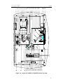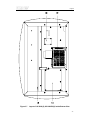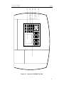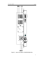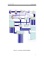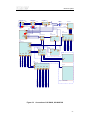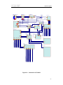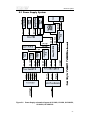
1
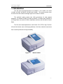
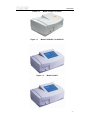
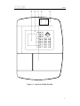
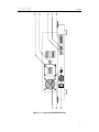
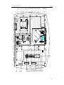
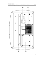
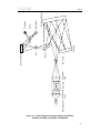
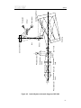
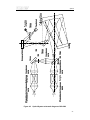
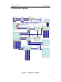
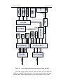
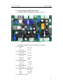
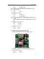
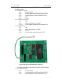
UNICO SQ Series
MODEL
UV-2800 / UV-2802 /UV-2802PC/UV-2802S/
UV-2802PCS / UV-3802 / UV-4802
SPECTROPHOTOMETER
SERVICE MANUAL
UNICO
182 Ridge Road, Suite E Dayton, NJ 08810 USA
732-274-1155 Fax: 732-274-1151 WEB: www.unicosci.com E-mail: [email protected]
CONTENTS
1. Introduction……………………………………………………
1
2. Specifications…………………………………………………
3
3. Layout…………………………………………………………
4
3.1 Layout of UV-2800……………………………………………………
4
3.2 Layout of UV-2802(S),UV-2802PC(S)………………………………
9
3.3 Layout of UV-3802……………………………………………………
15
3.4 Layout of UV-4802……………………………………………………
20
4. Optical System………………………………………………… 25
4.1 Incidence of Light………………………………………………………
25
4.2 Dispersion of Light……………………………………………………
25
4.3 Exit of Light……………………………………………………………
25
4.3.1 Exit of the Single Beam(UV-2800, UV-2802, UV-2802S)……………………
25
4.3.2 Exit of the Split Beam(UV-3802)………………………………………………
25
4.3.3 Exit of the Double Beam(UV-4802)……………………………………………
25
5. Electronic System……………………………………………
5.1 Power Supply System…………………………………………………
29
34
5.1.1 Power Supply PCB……………………………………………………………
36
5.1.2 Power Distributing PCB…………………………………………………………
37
5.2 Control and Drive System……………………………………………
38
5.2.1 Main CPU PCB…………………………………………………………………
41
5.2.2 Drive PCB………………………………………………………………………
44
5.2.3 Transferring PCB………………………………………………………………
46
5.3 Sampling and Signal Processing System……………………………
48
5.3.1 Amplifier PCB…………………………………………………………………
48
5.3.2 Slave Amplifier PCB……………………………………………………………
51
5.3.3 Slave CPU PCB………………………………………………………………
53
6. Trouble Shooting……………………………………………… 56
6.1 Tungsten lamp off……………………………………………………… 56
6.2 Deuterium lamp off……………………………………………………
57
6.3 Memory check failed…………………………………………………
58
6.4 Printer check failed……………………………………………………
58
6.5 Filter positioning failed………………………………………………… 59
6.6 Light source positioning failed………………………………………
60
6.7 Auto-cell positioning failed……………………………………………
61
6.8 Slit positioning failed…………………………………………………
62
6.9 Search 656.1nm failed………………………………………………
63
6.10 “Please restart” warning……………………………………………
64
6.11 “Battery low” warning…………………………………………………
64
6.12 Save or load file failed………………………………………………
64
6.13 Get dark current for a long time……………………………………
65
6.14 No backlight on LCD Display………………………………………
66
6.15 Backlight OK, but nothing display on LCD Display………………
67
6.16 “Energy low” warning after blanking………………………………
68
6.17 “Energy too low” warning……………………………………………
69
6.18 No DC +12V on PCB SST8.412.113………………………………
70
7. Maintenance…………………………………………………… 71
7.1 Working Environment…………………………………………………
71
7.2 Replace Tungsten Lamp………………………………………………
71
7.3 Replace Deuterium Lamp……………………………………………
75
7.4 Replace Memory Battery……………………………………………
77
7.5 Upgrade Firmware……………………………………………………
78
7.6 Check Performance……………………………………………………
81
7.6.1 Prepare……………………………………………………………………………
81
7.6.2 Check Wavelength Accuracy…………………………………………………
81
7.6.3 Check Stray Light………………………………………………………………
82
7.6.4 Check Absorbance Accuracy…………………………………………………
82
7.6.5 Check Dark Current……………………………………………………………
82
7.6.6 Check Energy Profile……………………………………………………………
83
Appendix…………………………………………………………… 84
Order NO. List of UV-2800…………………………………………………
84
Order NO. List of UV-2802, UV-2802PC…………………………………
85
Order NO. List of UV-2802S, UV-2802PCS………………………………
86
Order NO. List of UV-3802…………………………………………………
87
Order NO. List of UV-4802…………………………………………………
88
Introduction
1. Introduction
The SQ series Spectrophotometer are available in five models, the model
UV-2800, UV-2802, UV-2802S, UV-3802 and UV-4802. This series products cover
the Ultra Violet and Visible wavelength regions from 190nm to1100nm.
The analytical grating system has 1200 grooves/mm for high spectral
dispersion. The models UV-2800, UV-2802,UV-2802PC, UV-2802S and UV-2802PCS
are Single Beam, the model UV-3802 is Split Beam and the model UV-4802 is Double
Beam.
The SQ series Spectrophotometer used Double CPU, RTOS, High Precision
A/D and 320×240 dot matrix LCD Display(320X240). All of these made the instruments
have excellent performance and good stability.
Figure 1.1
Model UV-2800
-1-
Introduction
Figure 1.2
Figure 1.3
Model UV-2802, UV-2802S
Model UV-2802PC, UV-2802PCS
Figure 1.4
Model UV-3802
-2-
Introduction
Figure 1.5
Model UV-4802
-3-
UV-2802PC UV-2802PCS
20kg
21kg
22kg
21kg
RS-232, Centronics Parallel Port
Data Output
Weight
Tungsten lamp, Deuterium lamp
Light Source
22kg
620X400X280
±0.004A
Baseline Straight
545X425X260
±0.002A/h@500nm
Stability
Dimensions
±0.5%T
Photometric Accuracy
PC Monitor
0-200%T, -0.3-3.0A, 0-9999C
≤0.15%T@220nm&340nm
LCD(320×240), DMF50083
Photometric Range
Stray Light
Display
0.3nm
190-1100nm
0.5, 1, 2, 4nm
0.5nm
1.8nm
23kg
24kg
≤0.1%T@220nm&340nm
LCD(320×240), DMF50174
1.8nm
system1200 lines/mm
system1200 lines/mm
Wavelength Reatability
0.5, 1, 2, 4nm
Double beam, grating
Split beam, grating
±0.5nm
1.8nm
UV-4802
UV-3802
±0.8nm
4nm
UV-2802S
Single beam, grating system1200 lines/mm
UV-2802
Wavelength Accuracy
Wavelength Range
Spectrum Bandwidth
Optical System
UV-2800
Specifications
2. Specifications
-4-
Layout
3. Layout
3.1 Layout of UV-2800
1. Cooling Fan
3. Tungsten Lamp(W Lamp)
5. D2/W Power Supply PCB
7. Transformer
9. Lamp Limit Switch
11. Deuterium Lamp(D2 lamp)
13. Monochromator
15. Movable Nut
17. Sine Bar
19. Motor2(Wavelength)
21. Photo-couple1(Wavelength)
23. Shield Cover
25. Motor3(Filter)
27. Condenser Lens
29. Sample Compartment
31. Lamp Source Room
33. Light Blocking Plate
35. Power Distributing PCB
37. Main CPU PCB
39. LCD Screen(320x240 dots)
41. Sample Compartment Lid
43. Upper case
45. Viewing Hole
47. 232 Serial Port Interface
49. Power Switch
51. 110V/220V Selector
2. Concave Mirror
4. Heat Radiator
6. Motor1(Lamp Change)
8. Mirror1(Lamp Change)
10. Light Blocking Shelf
12. Entrance Slit
14. Monochromator Cover
16. Screw Thread Pole
18. Drive PCB
20. Synchro-Strap
22. Pull-Push Rod
24. Photo-couple2(Filter)
26. Amplifier PCB
28. 4-cell Sample Holder
30. Slave CPU PCB
32. Auto-cell Changer Connector
34. Rectifier
36. Switch Power Supply
38. Program Switch for Software Update
40. Keypad
42. Transferring PCB(In Upper Case)
44. Viewing Plate
46. Contrast Potentiometer for LCD
48. Printer Interface
50. Power Socket with Fuse with Fuse
-5-
Figure 3.1
29
28
27
26
25
24
23
22
33
32
31
30
34
8
9
10
11
12
13
14
15
16
17
18
19
20
21
1
2
3
4
5
6
7
Layout
Layout of UV-2800 Inside Top View
-6-
Layout
Figure 3.2
Layout of UV-2800 Inside Bottom View
-7-
43
42
41
40
39
Layout
Figure 3. 3 Layout of UV-2800 Top View
-8-
48
47
46
45
44
Layout
49
50
51
230V
Figure 3. 4 Layout of UV-2800 Back View
-9-
Layout
3.2 Layout of UV-2802(S), UV-2802PC(S)
1. Cooling Fan
3. Tungsten Lamp(W Lamp)
5. D2/W Power Supply PCB
7. Transformer
9. Lamp Limit Switch
11. Deuterium Lamp(D2 lamp)
13. Monochromator
15. Sine Bar
17. Movable Block
19. Gear
21. Photo-coupler1(Wavelength)
23. Auto-cell Changer Connector
25. Photo-coupler2(Filter)
27. Shield Cover
29. Condenser Lens
31. Slit Switch Equipment *
33. Photo-coupler4(Slit) *
35. Lamp Source Room
37. Light Blocking Shelf2
39. Power Distributing PCB
41. Main CPU PCB
43. LCD Display(320X240)
**
45. Sample Compartment Lid
47. Upper Case
49. Viewing Hole
51. 232 Serial Interface
53. Power Switch
55. 110V/220V Selector
Note:
2. Concave Mirror
4. Heat Radiator
6. Motor1(Lamp Change)
8. Mirror1(Lamp Change)
10. Light Blocking Shelf1
12. Entrance Slit
14. Fortified Board
16. Screw Thread Pole
18. Wavelength Limit switch
20. Motor2(Wavelength)
22. Drive PCB
24. Pull-Push Rod
26. Motor3(Filter)
28. Amplifier PCB
30. Sample Compartment
32. 4-Cell Sample Holder
34. Motor4(Slit) *
36. Slave CPU PCB
38. Rectifier
40. Switch Power Supply
42. Program Switch for Software Update
44. Keypad **
46. Transferring PCB(In Upper Case) **
48. Viewing plate
50. Contrast Potentiometer for LCD
52. Printer Interface
54. Power Socket with Fuse
* Only for UV-2802S, UV-2802PCS
** Only for UV-2802, UV-2802S
- 10 -
Figure 3.5
20
21
22
30
29
28
27
26
25
24
23
32
36
35
37
38
1
2
3
4
5
6
7
8
9
10
11
12
13
14
15
16
17
18
19
Layout
Layout of UV-2802, UV-2802PC Inside Top View
- 11 -
Figure 3.6
20
21
22
36
35
34
33
32
31
30
29
28
27
26
25
24
23
37
38
1
2
3
4
5
6
7
8
9
10
11
12
13
14
15
16
17
18
19
Layout
Layout of UV-2802S, UV-2802PCS Inside Top View
- 12 -
Layout
Figure 3.7
Layout of UV-2802(S), UV-2802PC(S) Inside Bottom View
- 13 -
Figure 3.8
47
46
45
44
43
Layout
Layout of UV-2802(S) Top View
- 14 -
Layout
230V
Figure 3.9
Layout of UV-2802(S) , UV-2802PC(S) Back View
- 15 -
Layout
3.3 Layout of UV-3802
1. Cooling Fan
3. Tungsten Lamp(W Lamp)
5. D2/W Power Supply PCB
7. Transformer
9. Lamp Limit Switch
11. Deuterium Lamp(D2 lamp)
13. Monochromator
15. Sine Bar
17. Movable Block
19. Gear
21. Photo-coupler1(Wavelength)
23. Auto-cell Changer Connector
25. Photo-coupler2(Filter)
27. Shield Cover
29. Condenser Lens
31. Light Distribute Room
33. Condenser Lens
35. Lamp Source Room
37. Shield
39. Rectifier
41. Switch Power Supply
43. Program Switch for Software Update
45. Keypad
47. Transferring PCB(In Upper Case)
49. Viewing plate
51. Contrast Potentiometer for LCD
53. Printer Interface
55. Power Socket with Fuse
2. Concave Mirror
4. Heat Radiator
6. Motor1(Lamp Change)
8. Mirror1(Lamp Change)
10. Light Blocking Shelf1
12. Entrance Slit
14. Fortified Board
16. Screw Thread Pole
18. Wavelength Limit switch
20. Motor2(Wavelength)
22. Drive PCB
24. Pull-Push Rod
26. Motor3(Filter)
28. Main Amplifier PCB
30. Sample Compartment
32. 4-Cell Sample Holder
34. Slave Amplifier PCB
36. Slave CPU PCB
38. Light Blocking Shelf2
40. Power Distributing PCB
42. Main CPU PCB
44. LCD Display(320X240)
46. Sample Compartment Lid
48. Upper Case
50. Viewing Hole
52. 232 Serial Interface
54. Power Switch
56. 110V/220V Selector
- 16 -
37
36
35
34
33
32
31
30
29
28
27
26
25
24
23
38
39
20
21
22
1
2
3
4
5
6
7
8
9
10
11
12
13
14
15
16
17
18
19
Layout
Figure 3.10 Layout of UV-3802 Inside Top View
- 17 -
Layout
Figure 3.11 Layout of UV-3802 Inside Bottom View
- 18 -
48
47
46
45
44
Layout
Figure 3.12 Layout of UV-3802 Top View
- 19 -
Layout
230V
Figure 3.13 Layout of UV-3802 Back View
- 20 -
Layout
3.4 Layout of UV-4802
1. Cooling Fan
3. Tungsten Lamp(W Lamp)
5. D2/W Power Supply PCB
7. Transformer
9. Lamp Limit Switch
11. Deuterium Lamp(D2 lamp)
13. Monochromator
15. Sine Bar
17. Movable Block
19. Gear
21. Photo-coupler1(Wavelength)
23. Auto-cell Changer Connector
25. Photo-coupler2(Filter)
27. Shield Cover
29. Condenser Lens
31. Light Distribute Room
33. Slave Amplifier PCB
35. Reference Holder
37. Slave CPU PCB
39. Power Distributing PCB
41. Main CPU PCB
43. LCD Display(320X240)
45. Sample Compartment Lid
47. Upper Case
49. Viewing Hole
51. 232 Serial Interface
53. Power Switch
55. 110V/220V Selector
2. Concave Mirror
4. Heat Radiator
6. Motor1(Lamp Change)
8. Mirror1(Lamp Change)
10. Light Blocking Shelf1
12. Entrance Slit
14. Fortified Board
16. Screw Thread Pole
18. Wavelength Limit switch
20. Motor2(Wavelength)
22. Drive PCB
24. Pull-Push Rod
26. Motor3(Filter)
28. Main Amplifier PCB
30. Sample Compartment
32. Sample Holder
34. Lamp Source Room
36. Light Blocking Shelf2
38. Rectifier
40. Switch Power Supply
42. Program Switch for Software Update
44. Keypad
46. Transferring PCB(In Upper Case)
48. Viewing plate
50. Contrast Potentiometer for LCD
52. Printer Interface
54. Power Socket with Fuse
- 21 -
35
34
33
32
31
30
29
28
27
26
25
24
23
37
36
38
`
20
21
22
1
2
3
4
5
6
7
8
9
10
11
12
13
14
15
16
17
18
19
Layout
- 22 -
Layout
Figure 3.14 Layout of UV-4802 Inside Top View
- 23 -
Layout
Figure 3.15 Layout of UV-4802 Inside Bottom View
- 24 -
47
46
45
44
43
Layout
Figure 3.16 Layout of UV-4802 Top View
- 25 -
Layout
230V
Figure 3.17 Layout of UV-4802 Back View
- 26 -
Optical
4. Optical System
The optical system of SQ series Spectrophotometers are adopted littrow type
with 1200lines/mm grating, UV-2800, UV-2802,UV-2802PC, UV-2802S and
UV-2802PCS are Single Beam, the optical system schematic diagram are shown in
4.1. UV-3802 and UV-4802 are Split Beam and Double Beam, the optical system
schematic diagram are shown in 4.2 and 4.3.
4.1 Incidence of Light
The neutral light coming from the Tungsten lamp or the Deuterium lamp is
focused at the entrance slit of the monochrometer by the concave mirror.
4.2 Dispersion of Light
The light passed through the entrance slit , reflected by the collimating mirror
to analytical grating. The light is spectrally dispersed by the grating and reflected
collimating mirror to the exit slit.
4.3 Exit of Light
4.3.1 Exit of the Single Beam (UV-2800, UV-2802(S), UV-2802PC(S))
The light from the exit slit, through the condenser lens focused on the
sample, continue pass through the sample, the light finally to the
photodetector. Shown in Figure 4.1.
4.3.2 Exit of the Split Beam (UV-3802)
From the exit slit, the light was separated two path by the mirror, the main
light focused on the sample after it passed though the condenser lens,
continue pass through the sample, the light finally to the photodetector on the
main Amplifier PCB. The slave light passed though the condenser lens to the
photodetector on the Slave Amplifier PCB. Shown in Figure 4.2.
4.3.3 Exit of the Double Beam (UV-4802)
From the exit slit, the light was separated two paths by the mirror, the main
light focused on the sample after it passed though the condenser lens,
continue pass through the sample, the light finally to the photodetector on the
main Amplifier PCB. The slave light focused on the 2nd exit slit in the slave
light path, then focused on the reference after it passed though the slave
condenser lens, continue pass through the reference, the light finally to the
photodetector on the slave Amplifier PCB. Shown in Figure 4.3.
- 27 -
Photodetector Condenser Sample
Lens
Condenser
Lens
Slit Filter
Mirror
Slit
Concave Mirror
Grating
Collimatng Mirror
Deuterium
Mirror
Tungsten
Optical
Figure 4.1 Optical System schematic diagram of UV-2800,
UV-2802, UV-2802S, UV-2802PC, UV-2802PCS
- 28 -
Figure 4.2
Photodetector Condenser Sample
Lens
Mirror
Prismatic
Condenser Mirror Slit Filter
Lens
Condenser
Lens
Photodetector
Slit
Concave Mirror
Grating
Collimatng Mirror
Deuterium
Mirror
Tungsten
Optical
Optical System schematic diagram of UV-3802
- 29 -
Optical
Figure 4.3
Optical System schematic diagram of UV-4802
- 30 -
Electronic System
Power Switch
(R220-22C-11D)
1
2
4
5
115V/230 Selector
(L21-22A1)
Red
3
2
1
L
Blk
N
Yel/Grn
Blk
4
Connector
(4508A)
Brw
Transformor
6
Power Supply Socket
(3EGG1-2)
Red
5
Org
Wht,Brw,Org,Red
GND
Pur,Red
Blu,Blk
Yel,Org
Gry,Wht
J1
J6
J7
J8
J9
J1
J2
J4
J1 J2
PCB
(SST8.411.128A)
J11
Wht
Org
Blk
Red
(-12V) -V
(+12V) +V
COM
+5V
PCB
(SST8.413.104A)
J10
PCB
(SST8.411.130A)
J3
N
J2
J3
J4
J5
Red
Red
Wht
Wht
Yel/Grn
L
Yel/Grn
Yel/Grn
Switch Power
(T-60B)
PCB
(SST8.412.113)
Rectifier
Transistor2
Deuterium Lamp
J3
J3
J1
J31
CZ61
CZ41
CN2
CZ6
CN1
CZ3
CZ5
CZ4
CZ6
PCB
(SST8.414.103)
LCD
PCB
(SST8.417.102)
Keypad
CN2
J12
J9
Light Change Limit Switch
J6
Figure 5.1
Filter Photo-coupler(PCB:SST8.417.101)
J5
Wavelength Motor
Filter Moter
J4
J14
CN1
Light Change Motor
RS-232
J18
J17
CZ4
PCB
(SST8.412.314A)
CN1
Printer Port
LCD Contrast Adjuster
Program Switch
J3
J8
PCB
(SST8.417.100)
Transistor1
CZ2
Cooling Fan
Yel,Grn
CZ7
Tungsten Lamp
CZ1
Auto-cell Connector
Fuse
5H 250V ,3.15A
5. Electronic System
Connection of UV-2800
- 31 -
Power Switch
(R220-22C-11D)
1
115V/230 Selector
(L21-22A1)
Red
2
3
2
1
L
Blk
N
4
Yel/Grn
Blk
5
Connector
(4508A)
Brw
Transformor
6
Power Supply Socket
(3EGG1-2)
Red
4
5
Org
Wht,Brw,Org,Red
GND
PCB
(SST8.413.104A)
Pur,Red
Blu,Blk
Yel,Org
Gry,Wht
J1
J6
J7
J11
J8
J9
J1
J2
J4
J1 J2
J10
PCB
(SST8.411.130A)
Wht
Org
Blk
Red
(-12V) -V
(+12V) +V
COM
+5V
PCB
(SST8.411.128A)
J3
N
J2
J3
J4
J5
Red
Red
Wht
Wht
Yel/Grn
L
Yel/Grn
Yel/Grn
Switch Power
(T-60B)
PCB
(SST8.412.113)
Rectifier
Transistor2
Deuterium Lamp
J3
J3
J1
J31
CZ61
CZ41
CN2
CN1
CZ3
CZ5
CZ6
LCD
PCB
(SST8.414.104)
Keypad
Figure 5.2
J14
Wavelength Photo-coupler(PCB:SST8.415.001-D )
J9
J6
J5
J12
Light Change Limit Switch
Filter Photo-coupler(PCB:SST8.417.101)
Wavelength Motor
Filter Moter
CN1
J4
CN2
Light Change Motor
RS-232
J18
J17
CZ4
CZ6
CN1
Printer Port
LCD Contrast Adjuster
Program Switch
J3
J8
CZ4
PCB
(SST8.412.314A)
Transistor1
Yel,Grn
CZ2
PCB
(SST8.417.100)
Cooling Fan
CZ7
Tungsten Lamp
CZ1
Auto-cell Connector
Fuse
5H 250V ,3.15A
Electronic System
Only for UV-2802
Connection of UV-2802, UV-2802PC
- 32 -
Power Switch
(R220-22C-11D)
1
115V/230 Selector
(L21-22A1)
Red
2
3
2
1
L
Blk
N
4
Blk
5
Yel/Grn
Connector
(4508A)
Brw
Transformor
6
Power Supply Socket
(3EGG1-2)
Red
4
5
Org
Wht,Brw,Org,Red
GND
PCB
(SST5.413.104A)
Pur,Red
Blu,Blk
Yel,Org
Gry,Wht
J1
J6
J7
J11
J8
J9
J1
J2
J4
J1 J2
J10
PCB
(SST8.411.130A)
Wht
Org
Blk
Red
(-12V) -V
(+12V) +V
COM
+5V
PCB
(SST8.411.128A)
J3
N
J2
J3
J4
J5
Red
Red
Wht
Wht
Yel/Grn
L
Yel/Grn
Yel/Grn
Switch Power
(T-60B)
PCB
(SST8.412.113)
Rectifier
Transistor2
Deuterium Lamp
J3
J3
J1
J31
CZ61
CZ41
CN2
CN1
CZ3
CZ5
CZ6
LCD
PCB
(SST8.414.104)
RS-232
Keypad
Figure 5.3
J7
Only for UV-2802S
Slit Motor
J14
Wavelength Photo-coupler(PCB:SST8.415.001-D )
J12
J9
J6
J5
J11
Slit Photo-coupler(PCB:SST8.415.001-D )
Light Change Limit Switch
Filter Photo-coupler(PCB:SST8.417.101)
Wavelength Motor
Filter Moter
CN1
J4
CN2
Light Change Motor
J18
J17
CZ4
CZ6
CN1
Printer Port
LCD Contrast Adjuster
Program Switch
J3
J8
CZ4
PCB
(SST8.412.314A)
Transistor1
Yel,Grn
CZ2
PCB
(SST8.417.100)
Cooling Fan
CZ7
Tungsten Lamp
CZ1
Auto-cell Connector
Fuse
5H 250V ,3.15A
Electronic System
Connection of UV-2802S, UV-2802PCS
- 33 -
Power Switch
(R220-22C-11D)
1
2
115V/230 Selector
(L21-22A1)
Red
3
2
1
L
Blk
N
4
Yel/Grn
5
Blk
Connector
(4508A)
Brw
Transformor
6
Power Supply Socket
(3EGG1-2)
Red
4
5
Org
Wht,Brw,Org,Red
GND
Yel/Grn
PCB
(SST8.411.128A)
PCB
(SST8.413.104A)
J5
J1
J6
J7
J2
J8
J1
J11
J2
J10
J9
J1
J4
Pur,Red
Blu,Blk
Yel,Org
Gry,Wht
(SST8.413.103A)
J2
J3
J4
J5
PCB
(SST8.411.130A)
Wht
Org
Blk
Red
(-12V) -V
(+12V) +V
COM
+5V
PCB
J1
J3
N
Yel/Grn
Red
Red
Wht
Wht
Yel/Grn
L
J2
Switch Power
(T-60B)
PCB
(SST8.412.113)
Rectifier
Transistor2
Deuterium Lamp
J2
J3
J3
J1
J31
CZ61
CZ41
CN2
CZ6
CN1
CZ3
CZ5
CZ4
CZ6
LCD
PCB
(SST8.414.104)
Keypad
J14
Wavelength Photo-coupler(PCB:SST8.415.001-D )
J12
Light Change Limit Switch
J6
J9
Filter Photo-coupler(PCB:SST8.417.101)
J5
Figure 5.4
Wavelength Motor
Filter Moter
CN1
J4
CN2
Light Change Motor
RS-232
J18
J17
CZ4
PCB
(SST8.412.314A)
CN1
Printer Port
LCD Contrast Adjuster
Program Switch
J3
J8
PCB
(SST8.417.100)
Transistor1
CZ2
Cooling Fan
Yel,Grn
CZ7
Tungsten Lamp
CZ1
Auto-cell Connector
Fuse
5H 250V ,3.15A
Electronic System
Connection of UV-3802
- 34 -
Power Switch
(R220-22C-11D)
1
115V/230 Selector
(L21-22A1)
Red
2
3
2
1
L
Blk
N
4
Yel/Grn
Blk
5
Connector
(4508A)
Brw
Transformor
6
Power Supply Socket
(3EGG1-2)
Red
4
5
Org
Wht,Brw,Org,Red
GND
Yel/Grn
PCB
(SST8.413.104A)
J1
J6
J7
J2
J8
J1
J11
J2
J10
J9
J1
J4
Pur,Red
Blu,Blk
Yel,Org
Gry,Wht
PCB
(SST8.411.128A)
J2
J3
J4
J5
PCB
(SST8.411.130A)
Wht
Org
Blk
Red
(-12V) -V
(+12V) +V
COM
+5V
PCB
(SST8.413.104A)
J1
J3
N
Yel/Grn
Red
Red
Wht
Wht
Yel/Grn
L
J2
Switch Power
(T-60B)
PCB
(SST8.412.113)
Rectifier
Transistor2
Deuterium Lamp
J2
J3
J3
J1
J31
CZ61
CZ41
CN2
CZ6
CN1
CZ3
CZ5
CZ4
CZ6
LCD
PCB
(SST8.414.104)
Keypad
J14
Wavelength Photo-coupler(PCB:SST8.415.001-D )
J9
J12
Light Change Limit Switch
J6
Figure 5.5
Filter Photo-coupler(PCB:SST8.417.101)
J5
Wavelength Motor
Filter Moter
CN1
J4
CN2
Light Change Motor
RS-232
J18
J17
CZ4
PCB
(SST8.412.314A)
CN1
Printer Port
LCD Contrast Adjuster
Program Switch
J3
J8
PCB
(SST8.417.100)
Transistor1
CZ2
Cooling Fan
Yel,Grn
CZ7
Tungsten Lamp
CZ1
Auto-cell Connector
Fuse
5H 250V ,3.15A
Electronic System
Connection of UV-4802
- 35 -
Electronic System
5.1 Power Supply System
Figure 5.6
Power Supply schematic diagram of UV-2800, UV-2802, UV-2802PC,
UV-2802S, UV-2802PCS
- 36 -
Electronic System
Figure 5.7
Power Supply schematic diagram of UV-3802, UV-4802
The power supply system of the SQ series are made up of two parts, the
transformer supplied for the light source as Tungsten lamp and Deuterium lamp,
and the Switch Power Supply supplied for the control system as CPU, Driver …,
- 37 -
Electronic System
and so on. The schematic diagrams are shown in figure 5.6 and 5.7.
5.1.1 Power Supply PCB(SST8.411.128A)
The layout of the Power Supply PCB is shown in figure 5.8
Figure 5.8
Layout of Power Supply PCB
The sockets description of the Power Supply PCB as follow:
J1---To Rectifier
Pin 1:
DC +18V
Pin (2, 3):
AC 15V
J2---From Transformer
Pin (1, 2):
AC 15V
J3---From Transformer
Pin (1, 4):
AC 18V
Pin (2, 5):
AC 18V
Pin 3, 6:
GND
J4---From Transformer
Pin (1, 4):
AC 250V
Pin (5, 6):
AC 105V
J5---From Transformer
Pin (1, 3):
AC 6V
J6---To 2SC2625 of Deuterium Lamp
Pin 1:
DC +46V
Pin 2:
DC +3.6V
Pin 3:
DC +3V
J7---To Deuterium Lamp
- 38 -
Electronic System
Pin 1:
DC +118V(+131V)
Pin 2:
DC +49V(+11.5V)
Pin 3:
DC +49V(+11.5V)
Note: When staring the Deuterium lamp, the voltage refer in the ( ).
J8---To Tungsten Lamp
Pin 1:
DC +11V
Pin 2:
GND
J9---From Main CPU PCB
Pin 1, 2:
DC +5V
Pin 3:
DC +3.85V(+5V)
Pin 4:
DC +5V(+3.85V)
Note: 1. If the voltage of pin 3 is +3.85V, the Deuterium lamps is on, or
it is off.
2. If the voltage of pin 4 is +5V, the Tungsten lamps is on, or it is
off.
J10---To 2SC2625 of Tungsten Lamp
Pin 1:
DC +18V
Pin 2:
DC +10.8V
Pin 3:
DC +10.5V
J11---To Cooling Fan
Pin 1:
DC +12V
Pin 2:
GND
5.1.2 Power Distributing PCB(SST8.411.130A)
The layout of the Power Distributing PCB is shown in figure 5.9
Figure 5.9 Layout of Power Distributing PCB
The sockets description of the Power Distributing PCB as follow:
J1---From Switch Power Supply
Pin 1:
DC -12V
Pin 2, 6, 7:
DC +5V
- 39 -
Electronic System
Pin 3, 4, 5:
DC +12V
Pin 8, 9, 10:
GND
J2---To (Main) Amplifier PCB
Pin 1:
DC +9V
Pin 2:
GND
Pin 3:
DC -9V
J3---To Transferring PCB(In Upper Case)
Pin (1, 3):
AC 1200V
J4---To Main CPU PCB
Pin 1, 2:
DC +12V
Pin 3, 4:
GND
Pin 5, 6:
DC +5V
J5---To Slave Amplifier PCB
Pin 1:
DC +9V
Pin 2:
GND
Pin 3:
DC -9V
5.2 Control and Drive System
The working principle as follow (shown in figure 5.10, 5.11 and 5.12):
1. User setup the “Test Parameters” by operating the Keypad. The main
CPU (on “Main CPU PCB”) command the motor to goto the setup
wavelength, select the correct light source and filter;
2. Halogen or deuterium lamp to supply the light, the Monochromator to
isolate the wavelength of interest and eliminate the unwanted second
order radiation, the sample compartment to accommodate the sample
solution;
3. The detector to receive the transmitted light and convert it to an
electrical signal, the slave CPU (on “Slave CPU PCB”) control to
amplifier the electrical signal and convert it to be digital signal, send it to
main CPU;
4. The main CPU gets the digital signal, process and outputs the results
(display, print or send to PC, and so on).
- 40 -
Keypad
Turn on/off
Light Souce
Switch Light
Source
Light
Source
LCD
Display
Go WL
Go Auto-Sample Holder
Sample
Compar
-tment
Printer
Port
Main Control System
Select Filter
Monochro
mator
RS-232
A/D and Signal
Process
Sampling and Pre-amplifier
Electronic System
Figure 5.10 Working Principle of UV-2800, UV-2802(S)
- 41 -
Keypad
Turn on/off
Light Souce
Switch Light
Source
Light
Source
LCD
Display
Go WL
Go Auto-Sample Holder
Sample
Compar
-tment
Printer
Port
Main Control System
Select Filter
Monochro
mator
RS-232
A/D and Signal
Process
Sampling and Pre-amplifier
(Main)
Sampling and Pre-amplifier
(Slave)
Electronic System
Figure 5.11 Working Principle of UV-3802
- 42 -
Keypad
Turn on/off
Light Souce
Switch Light
Source
Light
Source
LCD
Display
Go WL
Go Auto-Sample Holder
Sample
Compar
-tment
Printer
Port
Main Control System
Select Filter
Monochro
mator
RS-232
A/D and Signal
Process
Sampling and Pre-amplifier
(Slave)
Sampling and Pre-amplifier
(Main)
Electronic System
Figure 5.12 Working Principle of UV-4802
5.2.1 Main CPU PCB(SST8.412.113)
The layout of the main CPU PCB is shown in figure 5.13
- 43 -
Electronic System
Figure 5.13 Layout of Main CPU PCB
- 44 -
Electronic System
The sockets description of the main CPU PCB as follow:
CZ1---From Power Distributing PCB
Pin 1, 2:
DC +12V
Pin 3, 4:
GND
Pin 5, 6:
DC +5V
CZ2---To Slave CPU PCB
Pin 1:
Reset W78E52B on Slave CPU PCB
Pin 2:
Transfer signal to W78E52B on Slave CPU PCB
Pin 3:
Receive signal from W78E52B on Slave CPU PCB
Pin 4:
GND
Pin 5:
DC +5V
CZ3---To RS-232 Port
Pin 1:
GND
Pin 2:
Transfer signal
Pin 3:
Receive signal
CZ4---To Transferring PCB(In Upper Case)
Pin 1-8:
Output to signal Keypad
Pin 9-12:
Input signal from Keypad
CZ5---To Printer Port
Pin 1:
Pulse for read the data for printer
Pin 2-9:
Data bus
Pin 10:
Error detect. +5V indicate the printer is OK
Pin 11:
Busy detect. +5V indicate the printer is busy
Pin 12:
Reset the printer
Pin 15,16: GND
CZ6---To Transferring PCB(In Upper Case)
Pin 1-4, 13: Control signal of LCD
Pin 5:
DC +5V- -20.5V, contrast adjust
Pin 6:
DC +5V
Pin 7:
GND
Pin 8:
DC -20.5V
Pin 9-12:
Data bus
CZ7---To Power Supply PCB
Pin 1:
DC +5V(+3.85V). +5V: Tungsten lamps is on
Pin 2:
DC +3.85V(+5V). +3.85V Deuterium lamps is on
Pin 3, 4:
DC +5V
J3---To Auto-cell Connector
Pin 1-4:
Drive auto-sample Holder step motor
Pin 5:
DC +12V
J8---To Auto-cell Connector
Pin 1,2:
DC +5V(0V)
Pin 3:
DC +12V
Pin 4,5,6:
DC +5V
- 45 -
Electronic System
Pin 7:
GND
J17---To Program Switch for Software Update
Pin 1:
DC +5V (0V). +5V: instrument is working on “Test
Mode”, or it working on “Program Mode”.
Pin 2:
GND
J18---To Contrast Adjustor
Pin 1:
DC -20.5V
Pin 2:
DC +5V- -20.5V, contrast adjust
Pin 3:
DC +5V
CN1---To Drive PCB
Pin 1-4:
Control slit step motor
Pin 5:
Slit Photo-coupler signal
Pin 6:
Wavelength Photo-coupler and limit switch signal
Pin 7:
Filter Photo-coupler signal
Pin 8:
Lamp limit switch signal
Pin 9,11,13,15: GND
Pin 10,12,14,16: DC +12V
CN2---To Drive PCB
Pin 1:
GND
Pin 2:
DC +5V
Pin 3-6:
Control wavelength step motor
Pin 7-10:
Control filter step motor
Pin 11-14:
Control lamp Change step motor
5.2.2
Drive PCB(SST8.414.103 or SST8.414.104)
The layout of the Drive PCB is shown in figure 5.14, 5.15 and 5.16
Figure 5.14 Layout of UV-2800 Drive PCB
- 46 -
Electronic System
Figure 5.15 Layout of UV-2802S,UV-2802PCS Drive PCB
Figure 5.16 Layout of UV-2802, UV-2802PC, UV-3802, UV-4802 Drive PCB
The sockets description of the Drive PCB as follow:
CN1---From Main CPU PCB
Pin 1-4:
Control slit step motor
Pin 5:
Slit Photo-coupler signal
Pin 6:
Wavelength Photo-coupler and limit switch signal
Pin 7:
Filter Photo-coupler signal
Pin 8:
Lamp limit switch signal
- 47 -
Electronic System
Pin 9,11,13,15: GND
Pin 10,12,14,16: DC +12V
CN2--- From Main CPU PCB
Pin 1:
GND
Pin 2:
DC +5V
Pin 3-6:
Control wavelength step motor
Pin 7-10:
Control filter step motor
Pin 11-14:
Control lamp Change step motor
J4---To lamp Change step motor
Pin 1-4:
Drive slit step motor
Pin 5:
DC +12V
J5---To filter step motor
Pin 1-4:
Drive filter step motor
Pin 5:
DC +12V
J6---To wavelength step motor
Pin 1-4:
Drive wavelength step motor
Pin 5:
DC +12V
J7---To slit step motor
Pin 1-4:
Drive slit step motor
Pin 5:
DC +12V
J9---To filter Photo-coupler
Pin 1:
GND
Pin 2:
DC +5V (0V). 0V: only at initiative position
Pin 3:
DC +1.2V
J11---To slit Photo-coupler
Pin 1:
GND
Pin 2:
DC 0V (+5V). +5V: only at initiative position
Pin 3:
DC +1.2V
J12---To lamp limit switch
Pin 1:
GND
Pin 2:
DC +5V (0V). 0V: only at initiative position
Pin 3:
DC +5V
J14---To wavelength Photo-coupler and limit switch
Pin 1:
GND
Pin 2:
DC 0V (+5V). +5V: when the mobile block at start or
end point
Pin 3:
DC +5V
5.2.3
Transferring PCB(In Upper Case)(SST8.417.100)
The layout of the Transferring PCB(In Upper Case) is shown in figure
5.17
- 48 -
Electronic System
Figure 5.17 Layout of Transferring PCB(In Upper Case)
The sockets description of the Transferring PCB(In Upper Case) as
follow:
J3---From Power Distributing PCB
Pin (1, 3):
AC 1200V
J31---To LCD back light
Pin (1, 2):
AC 1200V
CZ4---From Main CPU PCB
Pin 1-8:
Output signal to Keypad
Pin 9-12:
Input signal from Keypad
CZ41---To keypad
Pin 1-8:
Output signal to Keypad
Pin 9-12:
Input signal from Keypad
CZ6--- From Main CPU PCB
Pin 1-4, 13: Control signal of LCD
Pin 5:
DC +5V- -20.5V, contrast adjust
Pin 6:
DC +5V
Pin 7:
GND
Pin 8:
DC -20.5V
Pin 9-12:
Data bus
CZ61--- To LCD Display(320X240)
Pin 1-4, 13: Control signal of LCD
Pin 5:
DC +5V- -20.5V, contrast adjust
Pin 6:
DC +5V
Pin 7:
GND
Pin 8:
DC -20.5V
Pin 9-12:
Data bus
- 49 -
Electronic System
5.3 Sampling and Signal Processing System
The working principle as follow:
1. The photo-detector receives the light signal, converts it to be electrical signal
(analog signal);
2. Amplifier the analog signal, the multiple is control by the CPU on the Slave
CPU PCB (W78E52B);
3. The A/D converts analog signal to be digital signal;
4. The Slave CPU send the digital signal to the main CPU.
5.3.1
Amplifier PCB(SST8.413.104A)
The layout of the Amplifier PCB of UV-2800, UV-2802, UV-2802PC,
UV-2802S and UV-2802PCS (R17—R20 of UV-2802S and UV-2802PCS are
different from others) is shown in figure 5.18, UV-4802 is shown in figure
5.19:
Figure 5.18 Layout of UV-2800, UV-2802, UV-2802S,
UV-2802PC, UV-2802PCS, UV-3802 Amplifier PCB
The sockets description of the Amplifier PCB of UV-2800, UV-2802(S),
UV-3802 as follow:
J1---From Power Distributing PCB
Pin 1:
DC +9V
Pin 2:
GND
Pin 3:
DC -9V
J2---From Slave CPU PCB
- 50 -
Electronic System
Pin 1:
GND
Pin 2:
Analog signal from pin 6 of OP07
Pin 8:
DC +5V
Pin 3-7:
Control amplifier multiple from Slave CPU PCB
The amplifier multiple of UV-2800, UV-2802(S) Amplifier PCB as follow:
Amplifier
multiple
0
1
2
3
4
5
6
7
8
9
10
Note:
Pin 3
Pin 4
Pin 5
Pin 6
Pin 7
0
0
1
1
1
1
1
1
1
1
1
0
1
0
1
1
1
1
1
1
1
1
0
0
0
0
0
0
0
1
1
1
1
0
0
0
0
0
1
1
0
0
1
1
0
0
0
0
1
0
1
0
1
0
1
1.
0:
Logic low (0V) 1:
Logic high (+5V)
The amplifier multiple of UV-3802 Amplifier PCB as follow:
Amplifier
Pin 3
Pin 4
Pin 5
Pin 6
multiple
0
1
1
0
0
1
1
1
0
0
2
1
1
0
1
3
1
1
0
1
4
1
1
1
0
5
1
1
1
0
6
1
1
1
1
7
1
1
1
1
8
1
1
1
1
9
1
1
1
1
10
1
1
1
1
Note:
1.
0:
Logic low (0V) 1:
Pin 7
0
1
0
1
0
1
0
1
1
1
1
Logic high (+5V)
- 51 -
Electronic System
Figure 5.19 Layout of UV-4802 Amplifier PCB
The sockets description of the Amplifier PCB of UV-4802 as follow:
J1---From Power Distributing PCB
Pin 1:
DC +9V
Pin 2:
GND
Pin 3:
DC -9V
J2---From Slave CPU PCB
Pin 1,2,3,5,7,9,11,13,15: GND
Pin 4:
Analog signal from pin 6 of OP07
Pin 16:
DC +5V
Pin 6,8,10,12,14:
Control amplifier multiple from Slave CPU
PCB
The amplifier multiple of UV-4802 Amplifier PCB as follow:
Amplifier
Pin 6
Pin 8
Pin 10
Pin 12
Pin 14
multiple
0
1
1
0
0
0
1
1
1
0
0
1
2
1
1
0
1
0
3
1
1
0
1
1
4
1
1
1
0
0
5
1
1
1
0
1
6
1
1
1
1
0
7
1
1
1
1
1
8
1
1
1
1
1
9
1
1
1
1
1
10
1
1
1
1
1
Note:
1.
0:
Logic low (0V) 1:
Logic high (+5V)
- 52 -
Electronic System
5.3.2
Slave Amplifier PCB(SST8.413.103A or SST8.413.104A)
Figure 5.20 Layout of UV-3802 Slave Amplifier PCB
The sockets description of the slave Amplifier PCB of UV-3802 as follow:
J1---From Power Distributing PCB
Pin 1:
DC +9V
Pin 2:
GND
Pin 3:
DC -9V
J2---From Slave CPU PCB
Pin 1:
GND
Pin 2:
DC +5V
Pin 3, 4:
Control amplifier multiple from Slave CPU PCB
The amplifier multiple of UV-3802 slave Amplifier PCB as follow:
Amplifier
Pin 3
Pin 4
1
0
0
2
0
1
3
1
0
4
1
1
Note:
1.
0:
Logic low (0V) 1:
Logic high (+5V)
- 53 -
Electronic System
Figure 5.21 Layout of UV-4802 Slave Amplifier PCB
The sockets description of the slave Amplifier PCB of UV-4802 as follow:
Pin 1:
DC +9V
Pin 2:
GND
Pin 3:
DC -9V
J2---From Slave CPU PCB
Pin 1,2,3,5,7,9,11,13:
GND
Pin 4:
Analog signal from pin 6 of OP07
Pin 6,8,10,12,14:
Control amplifier multiple from Slave CPU
PCB
The amplifier multiple of UV-4802 slave Amplifier PCB as follow:
Amplifier
Pin 6
Pin 8
Pin 10
Pin 12
Pin 14
multiple
0
1
1
0
0
0
1
1
1
0
0
1
2
1
1
0
1
0
3
1
1
0
1
1
4
1
1
1
0
0
5
1
1
1
0
1
6
1
1
1
1
0
7
1
1
1
1
1
8
1
1
1
1
1
9
1
1
1
1
1
10
1
1
1
1
1
Note:
1.
0:
Logic low (0V) 1:
Logic high (+5V)
- 54 -
Electronic System
5.3.3
Slave CPU PCB(SST8.412.314)
The layout of the slave CPU PCB is shown in figure 5.22, 5.23, 5.24.
Figure 5.22 Layout of UV-2800, UV-2802(S) Slave CPU PCB
Figure 5.23 Layout of UV-3802 Slave CPU PCB
- 55 -
Electronic System
The sockets description of the slave CPU PCB of UV-2800, UV-2802(S),
UV-3802 as follow:
J1---From Main CPU PCB
Pin 1:
Reset W78E52B
Pin 2:
Receive signal from W77E58 on Main CPU PCB
Pin 3:
Transfer signal to W77E58 on Main CPU PCB
Pin 4:
GND
Pin 5:
DC +5V
J2---To Slave Amplifier PCB
Pin 1:
GND
Pin 2:
Analog signal from pin 6 of OP07
Pin 3,4:
Control amplifier multiple of Slave Amplifier PCB
J3---To Amplifier PCB
Pin 1:
GND
Pin 2:
Analog signal from pin 6 of OP07
Pin 8:
DC +5V
Pin 3-7:
Control amplifier multiple of Amplifier PCB
Figure 5.24 Layout of UV-4802 Slave CPU PCB
The sockets description of the slave CPU PCB of UV-4802 as follow:
J1---From Main CPU PCB
Pin 1:
Reset W78E52B
Pin 2:
Receive signal from W77E58 on Main CPU PCB
Pin 3:
Transfer signal to W77E58 on Main CPU PCB
- 56 -
Electronic System
Pin 4:
GND
Pin 5:
DC +5V
J2-- To Slave Amplifier PCB
Pin 1,2,3,5,7,9,11,13:
Pin 4:
Pin 6,8,10,12,14:
GND
Analog signal from pin 6 of OP07
Control amplifier multiple of
Amplifier PCB
J3--- To Amplifier PCB
Pin 1,2,3,5,7,9,11,13,15: GND
Pin 4:
Analog signal from pin 6 of OP07
Pin 6,8,10,12,14,16:
Control amplifier multiple of
Amplifier PCB
Slave
Slave
- 57 -
Trouble Shooting
6. Trouble Shooting
6.1 Tungsten lamp off
- 58 -
Trouble Shooting
6.2 Deuterium lamp off
Deuterium lamp off
DC +49V on pin 2,3 of J7 on PCB
SST8.411.128A OK?
Y
1.Solving the wiring from J7
to deuterium lamp
2.Replace deuterium lamp
N
DC +0.7V between pin 2,3(B,E) and
DC +43V between pin 1,3(CE) of J6
on PCB SST8.411.128A OK?
1.Solving the wiring from J6
to 2SC2625
2.Replace 2SC2625
Y
Y
DC +46V on pin 1 of J6 on
PCB SST8.411.128A OK?
N
N
1. Solving the wiring of J5
on PCB SST8.411.128A
2. Replace transformer.
N
AC 5.5V between pin 1,2 of
J5 on PCB SST8.411.128A
OK?
Y
1. Solving the wiring of J4
on PCB SST8.411.128A
2. Replace transformer.
N
AC 250V between pin 1,2
and AC95V between pin 3,5
of J4 on PCB
SST8.411.128A OK?
Y
DC +3.85V on pin 3 of J9 on PCB
SST8.411.128A OK?
Y
Replace PCB
SST8.411.128A
Y
Solving the wiring from CZ7
to J9 on PCB
SST8.411.128A
N
DC +3.85V on pin 2 of CZ7 on PCB
SST8.412.113 OK?
N
Replace PCB SST8.412.113
- 59 -
Trouble Shooting
6.3 Memory check failed
6.4 Printer check failed
Note: It is recommended to connect the M501 to printer with
cable after both are powered on!
- 60 -
Trouble Shooting
6.5 Filter check failed
Filter positioning failed
Filter motor works OK?
N
Y
Y
DC +1.2V on pin 3 of J9 on PCB
SST8.414.103(104) OK?
1. Solving the wiring of filter
motor
2. Solving the wiring of CN2
on PCB SST8.414.103(104)
3. Replace PCB
SST8.414.103(104)
N
4.Replace filter motor
5.Replace PCB
SST8.412.113
Y
The voltage level on pin 2 of J9
on PCB SST8.414.103 changes
within 0— 3.2V during the filter
positioning?
Y
1. Solving the wiring of CN1 on
PCB SST8.414.103(104)
2. Replace PCB
SST8.414.103(104)
3. Replace PCB SST8.412.113
DC +12V on pin 5 of J5 on
PCB SST8.414.103(104)
OK?
N
N
DC +12V on pin 1 of CZ1 on
PCB SST8.412.113 OK?
N
Refer 6.18
1. Solving the wiring of J9 on
PCB SST8.414.103(104)
2. Replace photo-coupler.
1. Solving the wiring CN1 on
PCB SST8.414.103(104) to
PCB SST8.412.113
2. Replace PCB
SST8.414.103(104)
Y
1. Solving the wiring of CN2
on PCB SST8.414.103(104)
2. Replace PCB
SST8.414.103(104)
3.Replace PCB
SST8.412.113
- 61 -
Trouble Shooting
6.6 Light source check failed
Light Source positioning failed
Light change motor works OK?
N
Y
DC +5V on pin 3 of J12 on PCB
SST8.414.103(104) OK?
Y
The voltage on pin 2 of J12 on
PCB SST8.414.103(104) is from
0— 5V when the limit switch (refer
item 9 of layout on page 3) is
pressed down
Y
1. Solving the wiring CN1 on PCB
SST8.414.103(104) to PCB
SST8.412.113
N
2. Replace PCB
N
SST8.414.103(104)
3. Replace PCB SST8.412.113
DC +12V on pin 5 of J4 on
PCB SST8.414.103(104)
OK?
Y
1. Solving the wiring of light
change motor
2. Solving the wiring of CN2
on PCB SST8.414.103(104)
3. Replace PCB
SST8.414.103(104)
4.Replace light change
N
motor
5.Replace PCB
SST8.412.113
DC +12V on pin 1 of CZ1 on
PCB SST8.412.113 OK?
N
Refer 6.18
Y
1. Solving wiring J12 on PCB
SST8.414.103(104) to lamp
change limit switch.
2. Replace lamp change limit
switch.
1. Solving the wiring CN1 on
PCB SST8.414.103(104) to
PCB SST8.412.113
2. Replace PCB
SST8.414.103(104)
1. Solving the wiring of CN2
on PCB SST8.414.103(104)
2. Replace PCB
SST8.414.103(104)
3.Replace PCB
SST8.412.113
- 62 -
Trouble Shooting
6.7 Auto-cell check failed
Auto-cell holder positioning failed
Auto-cell holder motor works OK?
N
Y
Y
The voltage level on pin 2 of J8 on
PCB SST8.412.113 changes within
0— 3.2V during the filter positioning?
N
1. Solving the wiring from auto-cell
holder to auto-cell holder connector
2. Solving the wiring from auto-cell
holder connector to J8 on PCB
SST8.412.113
3. Replace auto-cell holder photocoupler
DC +12V on pin 1 of CZ1 on
PCB SST8.412.113 OK?
Y
1. Solving the wiring from
auto-cell holder to auto-cell
holder connector
2. Solving the wiring from
auto-cell holder connector to N
J3 on PCB SST8.412.113
3. Replace auto-cell holder
motor
4.Replace PCB
ST8.412.113
Refer 6.18
1. Replace IC 8255 of U17 on PCB
SST8.412.113
2. Replace PCB ST8.412.113
- 63 -
Trouble Shooting
6.8 Slit check failed(Only for UV-2802S, UV-2802PCS)
- 64 -
Trouble Shooting
6.9 Search 656.1nm failed(“D2 Energy too low” display on top
side of right hand corner of the screen after finishing “Reset
WL” )
Search 656.1nm failed
Anything block off the beam in
the sample compartment?
Y
Take it away
N
Refer 6.2
N
Refer 6.6
N
Refer 6.5
N
Deuterium lamp on?
Y
Light Source positioning OK?
Y
Filter positioning OK?
Y
Wavelength motor works OK?
N
Y
1. Solving the wiring of J2 on
PCB SST8.413.104A
2. Replace PCB
SST8.413.104A
3. Replace PCB
SST8.412.314A
1. Solving the wiring of
wavelength motor
2. Replace PCB
SST8.414.103(104)
3. Replace PCB SST8.412.113
4. Replace wavelength motor
- 65 -
Trouble Shooting
6.10 “Please restart” warning
“ Please restart” display on
top right corner on LCD screen
The slice on the screw thread
pole stay in the photo-coupler?
N
Y
1. Solving the wiring of J14 on
PCB SST8.414.103(104).
2. Solving the wiring of CN2 on
PCB SST8.414.103(104).
3. Replace photo-coupler.
4. Replace PCB
SST8.411.103(104).
5. Replace IC 8255 of U17 on
PCB SST8.412.113.
6. Replace PCB ST8.412.113.
1. Solving the wiring of limit
switch to photo-coupler.
2. Solving the wiring of J14 on
PCB SST8.414.103(104).
3. Replace limit switch.
6.11 “Battery low” warning
6.12 Save or load file failed (keypad goes dead after the
key “Save” or “Load” is pressed)
Save or load file failed
Restart instrument, press
“ 7” in “ Main Menu” , press
“ F1” and select
“ yes” ,” yes” to format file
system
N
Replace U4 on PCB
SST8.412.113
- 66 -
Trouble Shooting
6.13 Get dark current for a long time
- 67 -
Trouble Shooting
6.14 No backlight of LCD Display
Turn on, LCD display have no backlight
AC 110V or 220V Power on?
N
Power on
N
Connect power cord
N
Replace fuse
N
Solving wiring from power
socket to the switch
power
N
Replace switch power
N
Solving wiring from J1 on
PCB SST8.411.130A to
switch power
N
Replace PCB
SST8.411.130A
N
Solving wiring from J3 on
PCB SST8.411.130A to
SST8.417.100
Y
Power cord connect OK?
Y
Fuse OK?
Y
AC 110V/220V input of Switch
Power OK?
Y
+5V of Switch Power output OK?
Y
+5V of J1 on PCB SST8.411.130A
OK?
Y
AC 1200V of J3 on PCB
SST8.411.130A OK?
Y
AC 1200V of J3 on PCB
SST8.417.100 OK?
Y
1. Solving wiring from LCD display
to J3 on SST8.417.100
2. Replace LCD display
- 68 -
Trouble Shooting
6.15 Backlight OK, but display nothing on LCD Display
- 69 -
Trouble Shooting
6.16 “Energy low” warning after blanking
Note: If measuring at less than 200nm or more than 1000nm,it is
possible to appear “Energy low” warning!
- 70 -
Trouble Shooting
6.17 “Energy too low” warning
Energy too low
Anything block off the beam in
the sample compartment?
Y
Take it away
Y
Used quartz
cuvette?
N
The wavelength at UV area?
N
N
The reference or sample
solution have high absorbency
against air?
Replace cuvette
Y
Y
N
Dilute reference or sample
solution
The reference or sample
solution have high
absorbency against air?
Y
N
Tungsten lamp on
Deuterium lamp on
N
N
Refer 6.1
Refer 6.2
Y
Filter positioning OK?
N
Refer 6.5
N
Refer 6.6
Y
Light source positioning
OK?
Y
Replace tungsten lamp(Vis
area) or deuterium lamp(UV
area)
- 71 -
Trouble Shooting
6.18 No DC +12V on PCB SST8.412.113
- 72 -
Maintenance
7. Maintenance
7.1 Working Environment
Placed the instrument on a clean non-vibrational table, the optimum
environment as follow: the temperature is between 5℃ to 35℃, the humidity is
no more than 85%, avoid direct strong light and air flow, the voltage stability is
greater than ±10% and the frequency stability is greater than ±1% of the power
supply, no strong magnetic field near the instrument. Always allow the instrument
to warm up for 20 minutes prior before do any test.
7.2 Replace Tungsten Lamp
CAUTION:
1.
2.
3.
HIGH VOLTAGE
Turn off and unplug the instrument.
Remove the cuvette holder rod by unscrewing the rod counterclockwise.
Remove the all screws around the sides of the spectrophotometer. Show in
Figure 7.1.
- 73 -
Maintenance
Figure 7. 1 Remove the cover screws
4.
Very carefully remove the cover of the instrument and place in right side of the
instrument. Show in Figure 7.2.
Figure 7. 2 Remove the cover
- 74 -
Maintenance
HINT: If it is necessary to remove the cover from the right side of the
instrument, carefully remove 3 connectors (CZ6, CZ4 and J3) on
PCB marked SST8.417.100 . Be sure to reconnect after replacing
the lamp! Show in Figure 7.3.
Figure 7.3
5.
Unplug J3, CZ4, CZ6
Remove the grey metal protection cover. Using screwdrivers remove the two
top screws and the two bottom screws, and then place the protective cover to
the side. Shown in Figure 7.4.
- 75 -
Maintenance
Figure 7.4
6.
7.
8.
9.
Remove the Lamp Cover
Remove the lamp from the ceramic base.
Insert the new lamp (Figure 7.5), pushing it in as far as it will go.
Figure 7.5 Tungsten Lamp
Re-fit the grey metal protection cover, temporarily re-fit the main cover and fix
with two screws, one each side.
Switch on and remove the grommet from the middle of the rear panel. You
- 76 -
Maintenance
can now look through the Viewing Hole and view the image of the lamp on the
slit. Check the lamp alignment shown in Figure 7.6. If the image is not
covering the slit, the lamp alignment needs adjustment. This requires running
the SQ series without the covers, with high voltages accessible, and so
should only be performed by a suitably qualified engineer.
If adjustment is required, remove the cover and grey protection cover and turn
on the instrument. Adjust to make the image central on the slit.
Install the grey metal protection cover and instrument cover.
Focus on the
slit
Figure 7.6
CAUTION:
Adjust Tungsten Lamp
DO NOT HANDLE THE LAMP WITH BARE FINGERS. USE
TISSUE OR CLOTH WHEN HANDLING LAMP. The oil from
your fingers can cause the lamp to burn out prematurely.
10. Re-fit all the screws around the sides of the spectrophotometer.
11. Install the gray metal protection cover and cover of instrument.
12. Re-set the Tungsten lamp usage time. Select Utility, lamp and re-set W lamp
usage time.
7.3 Replace Deuterium Lamp
- 77 -
Maintenance
1.
2.
Do the same step as 1-5 of 7.2 (replace Tungsten Lamp).
Disconnecting the connector J7 on the PCB marked SST8.411.128.
Unscrew the screw that holds the lamp bracket to the instrument base. Pull
the entire lamp and lamp holder assembly out. Shown in Figure 7.7.
Figure 7.7
3.
Take off the Deuterium Lamp
Replace the pre-aligned lamp with a lamp (Figure 7.8) provided by UNICO or
an authorized UNICO Service Provider. This comes pre-assembled with lamp
socket.
CAUTION:
THE LAMP MAY BE HOT!
POSSIBLE BURNS.
TAKE PRECAUTIONS TO PREVENT
- 78 -
Maintenance
Figure 7.8
4.
5.
6.
Reconnect the connector J7 to the PCB marked SST8.411.128.
Re-fit the grey metal protection cover. Temporarily re-fit the main cover and
fix with two screws, one each side.
Switch on and remove the grommet from the middle of the rear panel. You
can now look through the Viewing Hole and view the image of the lamp on
the slit. Check the lamp alignment Figure 7.9. If the image is not covering the
slit, the lamp alignment needs adjustment. This requires running the SQ
series without the covers, with high voltages accessible, and so should only
be performed by a suitably qualified engineer.
If adjustment is required, remove the cover and grey protection cover, put on
UV protection glasses and turn on the instrument. Adjust to make the image
central on the slit, Figure 7.9.
CAUTION:
7.
8.
9.
Deuterium Lamp
Wear UV protection glasses when replacing deuterium lamp.
Install the grey metal protection cover and cover of instrument.
Re-fit all the screws around the sides of the spectrophotometer.
Re-set the lamp usage time. Select Utility, lamp, and re-set D2 usage time.
- 79 -
Maintenance
Focus on the
slit
Figure 7.9
Adjust Deuterium Lamp
7.4 Replace Memory Battery
1.
Turn the spectrophotometer upside down onto a padded surface. Remove
the all screws around the sides of the spectrophotometer shown in Figure
7.10 and take away the bottom cover.
Figure 7. 10 Remove the bottom cover
- 80 -
Maintenance
2.
There is a round lithium battery on the main CPU PCB. Shown in Figure
7.11where the red arrow is pointed. The battery model is CR1220 with 3V
voltage from Panasonic.
Figure 7. 11 Battery Position
Note:
Since the capacitor will only be able to maintain power for 5-6
minutes, we suggest you follow the procedure.
1)
2)
With the power unplugged, remove the bottom cover.
Locate the battery to be replaced on the board. DO NOT REMOVE
IT
YET.
Make sure you have the replacement battery ready.
Turn on the spectrophotometer and keep it on for a few minutes.
Turn off the spectrophotometer.
Immediately after turning off the spectrophotometer, remove the old
battery and insert the new one. This MUST be completed within 3
minutes of the spectrophotometer being turned off.
3)
4)
5)
6)
Note:
3.
Failure to follow the correct battery replacement procedure may
result in saved data being lost and a possible PC software
communication problem. It is recommended to transfer the data
saved in the memory to computer with PC download software
before replace battery.
Replace the bottom cover on the spectrophotometer, ensuring that all the star
washers are in position.
7.5 Upgrade Firmware
1.
Turn round spectrophotometer to find the switch shown in Figure 7.12 on the
- 81 -
Maintenance
base that controls spectrophotometer to run in normal or upgrading status.
Convert the switch to upgrading status.
Figure 7. 12
2.
Connect spectrophotometer to the computer with the correct RS232 cable.
Note:
3.
It is recommended that you connect spectrophotometer to Comm1
of your computer.
Before updating the software, save or copy the folder “Update” UNICO
provided to the disk C:/ of your computer. Usually there are five files in the
folder “Update” which are respectively Flash-UNICO.exe, *.H00, *.H01, *.H02
and *.H03 (*.H00, *.H01, *.H02 and *.H03 is different base your instrument
model.). After updating, two more files are created automatically, one is
UV2800.bin, another is serial.ini.
Note:
4.
5.
Normal/Program Switch for Software Update
The original serial number of spectrophotometer is stored in
serial.ini.
Open the folder “Update” and double click on the icon “Flash- UNICO”.
The “System updating program for UNICO” screen will appear. Shown in
Figure 7.13.
Figure 7. 13
Upgrade Form
- 82 -
Maintenance
6.
7.
8.
Click to select instrument model in Model Selection. Click on the small
pull-down triangle on the right to select the comm. port (Comm1 default.)
There are 4 comm. ports available. It depends on which comm. port you
connected between the computer and spectrophotometer.
Click on the ellipse icon “Load”, then only select the file “*.H00” in the folder
“Update”, click on “Open” to load.
Turn on spectrophotometer, the screen will display as below (Figure 7.14)
and wait for upgrading.
Figure 7. 14 Upgrade State
9.
Click on the button “Upload SN” in OEM information, the original serial
number of spectrophotometer will appear in line 1 – line 3 and is stored in
serial.ini . shown in Figure 7.15. If you do not have the original serial number,
please contact UNICO.
Figure 7. 15 Upload SN
10. Click on the ellipse icon “flash” on the left to start.
- 83 -
Maintenance
Figure 7. 16 Upgrading
Note:
Do not click on any icon during the process of upgrading.
11. After beeping three times, the software is upgraded successfully, turn off the
spectrophotometer, and then change the switch on the base of
spectrophotometer to the normal position.
12. Turn on the spectrophotometer, it will run with the new software.
13. It is highly recommended that, following software upgrading, you select
“calibration system” after the self-testing process, shown in Figure 7.17.
Figure 7. 17 Calibrating
7.6 Check Performance
7.6.1
1.
2.
3.
Prepare
Switch on and wait for 15 minutes. Ensure beam is clear.
Select “system calibration” yes.
When main menu appears at the end of calibration.
7.6.2
Check Wavelength Accuracy
- 84 -
Maintenance
1.
2.
3.
4.
5.
6.
7.
8.
9.
Prepare (Refer 7.6.1).
Press 3 to select “WL Scan”, press “F1” to setup, set the parameter as
follow, press “Enter” to finished setup.
Scan from: 400
Scan to: 300
Scan Step: 0.1
Scan Speed: HI
Ensure beam is clear. Press “0Abs” to scan blank.
Insert holmium filter. Press “Start”.
When scan complete, press “F3”: Search, Press “▼”, record wavelength
of holmium peak (specification: 360.9 ±1nm).
Press “ESC”, press “F1” to setup, set the parameter as follow, press
“Enter” to finished setup.
Scan from: 850
Scan to: 750
Scan Step: 0.1
Scan Speed: HI
Ensure beam is clear. Press “0Abs” to scan blank.
Insert didymium filter. Press “Start”.
When scan complete, press “F3”: Search, Press “▼”, record wavelength
of didymium peak (specification: 807.1 ±1nm).
7.6.3
Check Stray Light
1.
Prepare (Refer 7.6.1).
2.
Press “Setλ”, input 340, press “Enter” to go to 340nm.
3.
4.
5.
6.
Ensure beam is clear. Press 1 to “Basic Mode” and automatic blanking.
Insert GG375 filter.
Record stray light at 340nm (specification >3A, <0.1%T).
Remove filter.
7.
Press “Setλ”, input 220, press “Enter” to go to 220nm.
8.
9.
Insert WG295 filter.
Record stray light at 220nm (specification >3A, <0.1%T).
7.6.4
Check Absorbance Accuracy
1.
2.
Prepare (Refer 7.6.1).
Fit neutral density filters, blank, 0.5A, 1A, 2A in cell changer and move
blank into beam
3.
Press “Setλ”, input 546, press “Enter” to go to 546nm.
4.
Push filters into beam and record values. Compare the results with the
calibrated absorbance (specification <±1%A, so <±0.005A at 0.5A,
<±0.010A at 1A, <±0.020A at 2A).
- 85 -
Maintenance
7.6.5
1.
2.
3.
4.
Prepare (Refer 7.6.1).
Press 7 to select Utility.
Press “▲”, “Print”, to select diagnostic menu (Note: Sometimes this
page has a bar at the top and only the serial number below, instead
of the diagnostic menu.)
Press 5 to select “Check Dark Current” (even if “Check Dark Current” is
not displayed). A table of Gain, Energy, will be produced (The minimum
at Gain 0 should be greater than or equal to 1. The maximum at Gain 10
should be 2000 to 4000).
7.6.6
1.
2.
3.
4.
5.
Check Dark Current
Check Energy Profile
Prepare (Refer 7.6.1).
Press 3 to select “WL Scan”, press “F1” to setup, set the parameter as
follow, press “Enter” to finished setup.
Scan from: 1100
Scan to: 190
Scan Step: 0.5
Scan Speed: HI
Press 6, Press “Enter” to select ADEX: 1.
The wavelength will go to 1100nm and the energy profile will be
produced.
Record the maximum value around 550nm (25% to 60% full scale).
Record the maximum value below 340nm (5% to 10% full scale).
(For 2nm bandwidth, the energy will be approximately half these values)
- 86 -
Appendix
Appendix
Order No. List of UV-2800
PART NUMBER
SQ5-411-029
SQ5-411-030
SQ5-412-021
SQ5-412-022
DESCRIPTION OR PCB NO.
SST8.411.128
SST8.411.128A
SST8.411.130
SST8.411.130A
SST8.412.113
SST8.412.314
SST8.412.314A
SQ5-413-025
SST8.413.102
SQ5-414-012
SST8.414.103
SQ5-417-006
SST8.417.100
SQ5-415-007
SST8.417.101
SQ5-415-008
SST8.417.102
SQ6-491-317
Cooling Fan
SQ6-491-314
Transistor1(W Lamp)
SQ6-491-313
Transistor2(D2 Lamp)
SQ0-001-001
Rectifier
SQ6-491-324
Motor1(Lamp Change)
SQ6-491-308
Motor2(Wavelength)
SQ6-491-309
Motor3(Filter)
SQ0-002-001
W Lamp
SQ6-491-312
D2 Lamp
SQ6-491-315
Limit Switch
SQ6-491-307
LCD(320X240, DMF50081)
SQ6-491-320
Transformer
SQ0-003-001
Switch Power Supply(T-60B)
- 87 -
Appendix
Order No. List of UV-2802, UV-2802PC
PART NUMBER
SQ5-411-029
SQ5-411-030
SQ5-412-021
SQ5-412-022
DESCRIPTION OR PCB NO.
SST8.411.128
SST8.411.128A
SST8.411.130
SST8.411.130A
SST8.412.113
SST8.412.314
SST8.412.314A
SQ5-413-025
SST8.413.102
SQ5-414-013
SST8.414.104
SQ5-417-006
SST8.417.100
SQ5-415-007
SST8.417.101
SQ5-415-005
SST8.415.001-B
SST8.415.001-D
SQ6-491-341
Cooling Fan
SQ6-491-314
Transistor1(W Lamp)
SQ6-491-313
Transistor2(D2 Lamp)
SQ0-001-001
Rectifier
SQ6-491-335
Motor1(Lamp Change)
SQ6-491-308
Motor2(Wavelength)
SQ6-491-309
Motor3(Filter)
SQ0-002-001
W Lamp
SQ6-491-339
D2 Lamp
SQ6-491-315
Limit Switch1(Lamp Change)
SQ6-491-334
Limit Switch2(Wavelength)
SQ6-491-343
LCD(320X240, DMF50081)
SQ6-491-320
Transformer
SQ0-003-001
Switch Power Supply(T-60B)
- 88 -
Appendix
Order No. List of UV-2802S, UV-2802PCS
PART NUMBER
SQ5-411-029
SQ5-411-030
SQ5-412-021
SQ5-412-022
DESCRIPTION OR PCB NO.
SST8.411.128
SST8.411.128A
SST8.411.130
SST8.411.130A
SST8.412.113
SST8.412.314
SST8.412.314A
SQ5-413-019
SST8.413.102
SQ5-414-014
SST8.414.104
SQ5-417-006
SST8.417.100
SQ5-415-007
SST8.417.101
SQ5-415-005
SST8.415.001-B
SST8.415.001-D
SQ6-491-341
Cooling Fan
SQ6-491-314
Transistor1(W Lamp)
SQ6-491-313
Transistor2(D2 Lamp)
SQ0-001-001
Rectifier
SQ6-491-335
Motor1(Lamp Change)
SQ6-491-308
Motor2(Wavelength)
SQ6-491-309
Motor3(Filter)
SQ6-491-338
Motor4(Slit)
SQ0-002-001
W Lamp
SQ6-491-339
D2 Lamp
SQ6-491-315
Limit Switch1(Lamp Change)
SQ6-491-334
Limit Switch2(Wavelength)
SQ6-491-343
LCD(320X240, DMF50081)
SQ6-491-320
Transformer
SQ0-003-001
Switch Power Supply(T-60B)
- 89 -
Appendix
Order No. List of UV-3802
PART NUMBER
SQ5-411-029
SQ5-411-030
SQ5-412-021
SQ5-412-023
SQ5-413-025
SQ5-413-020
DESCRIPTION OR PCB NO.
SST8.411.128
SST8.411.128A
SST8.411.130
SST8.411.130A
SST8.412.113
SST8.412.314
SST8.412.314A
SST8.413.102
SST8.413.103
SST8.413.103A
SQ5-414-013
SST8.414.104
SQ5-417-006
SST8.417.100
SQ5-415-007
SST8.417.101
SQ5-415-005
SST8.415.001-B
SST8.415.001-D
SQ6-491-341
Cooling Fan
SQ6-491-314
Transistor1(W Lamp)
SQ6-491-313
Transistor2(D2 Lamp)
SQ0-001-001
Rectifier
SQ6-491-335
Motor1(Lamp Change)
SQ6-491-308
Motor2(Wavelength)
SQ6-491-309
Motor3(Filter)
SQ0-002-001
W Lamp
SQ6-491-339
D2 Lamp
SQ6-491-315
Limit Switch1(Lamp Change)
SQ6-491-334
Limit Switch2(Wavelength)
SQ6-491-343
LCD(320X240, DMF50174)
SQ6-491-320
Transformer
SQ0-003-001
Switch Power Supply(T-60B)
- 90 -
Appendix
Order No. List of UV-4802
PART NUMBER
SQ5-411-029
SQ5-411-030
SQ5-412-021
SQ5-412-025
DESCRIPTION OR PCB NO.
SST8.411.128
SST8.411.128A
SST8.411.130
SST8.411.130A
SST8.412.113
SST8.412.314
SST8.412.314A
SQ5-413-026
SST8.413.102(J2:16 pin)
SQ5-413-021
SST8.413.102(J2:14 pin)
SQ5-414-013
SST8.414.104
SQ5-417-006
SST8.417.100
SQ5-415-007
SST8.417.101
SQ5-415-005
SST8.415.001-B
SST8.415.001-D
SQ6-491-341
Cooling Fan
SQ6-491-314
Transistor1(W Lamp)
SQ6-491-313
Transistor2(D2 Lamp)
SQ0-001-001
Rectifier
SQ6-491-335
Motor1(Lamp Change)
SQ6-491-308
Motor2(Wavelength)
SQ6-491-309
Motor3(Filter)
SQ0-002-001
W Lamp
SQ6-491-339
D2 Lamp
SQ6-491-315
Limit Switch1(Lamp Change)
SQ6-491-334
Limit Switch2(Wavelength)
SQ6-491-343
LCD(320X240, DMF50174)
SQ6-491-320
Transformer
SQ0-003-001
Switch Power Supply(T-60B)
- 91 -