1
TC-610P Service Manual
Contents
Introduction… … … … … … … … … … … … … … … … … … … … … … … … … … … … … … … … … … … … … … … .1
Safety Information… … … … … … … … … … … … … … … … … … … … … … … … … … … … … … … … … … … … ..1
Radio Overview… … … … … … … … … … … … … … … … … … … … … … … … … … … … … … … … … … … … … ...2
Software Specifications… … … … … … … … … … … … … … … … … … … … … … … … … … … … … … … … … … 6
Circuit Description… … … … … … … … … … … … … … … … … … … … … … … … … … … … … … … … … … … .11
CPU Pins… … … … … … … … … … … … … … … … … … … … … … … … … … … … … … … … … … … … … … … … .21
TC-610P Parts List 1… … … … … … … … … … … … … … … … … … … … … … … … … … … … … … … … … … … 26
Adjustment Description… … … … … … … … … … … … … … … … … … … … … … … … … … … … … … … … … .72
Troubleshooting Flow Chart… … … … … … … … … … … … … … … … … … … … … … … … … … … … … … … .89
Disassembly and Assembly for Repair… … … … … … … … … … … … … … … … … … … … … … … … … … ..92
Exploded View… … … … … … … … … … … … … … … … … … … … … … … … … … … … … … … … … … … … … ..96
TC-610P Parts List 2… … … … … … … … … … … … … … … … … … … … … … … … … … … … … … … … … … … 97
Packing … … … … … … … … … … … … … … … … … … … … … … … … … … … … … … … … … … … … … … … … ..99
TC-610P PCB View… … … … … … … … … … … … … … … … … … … … … … … … … … … … … … … … … … … .100
TC-610P Level Diagram… … … … … … … … … … … … … … … … … … … … … … … … … … … … … … … … … 104
TC-610P Block Diagram… … … … … … … … … … … … … … … … … … … … … … … … … … … … … … … … 105
TC-610P VHF Schematic Diagram … … … … … … … … … … … … … … … … … … … … … … … … … … … … 106
TC-610P UHF Schematic Diagram… … … … … … … … … … … … … … … … … … … … … … … … … … … … 110
Specifications… … … … … … … … … … … … … … … … … … … … … … … … … … … … … … … … … … … … … 114
TC-610P Service Manual
Introduction
Manual Scope
This manual is intended for use by experienced technicians familiar with similar types of communication
equipment. It contains all service information required for the equipment and is current as of the
publication date.
Safety Information
The following safety precautions shall always be observed during operation, service and repair of this
equipment.
◇ This radio shall be serviced by qualified technicians only.
◇ Only use HYT supplied or approved batteries and chargers.
◇ To avoid electromagnetic interference and/or compatibility conflicts, turn off your radio in any
area where posted notices instruct you to do so. Turn off your radio before boarding an aircraft.
Any use of the radio must be in accordance with airline regulations or crew instructions.
◇ For vehicles with an air bag, do not place a radio in the area over an air bag or in the air bag
deployment area.
◇ Turn off your radio prior to entering any area with explosive and flammable materials.
◇ Do not charge or replace your battery in a location with explosive and flammable materials.
◇ Turn off your radio before entering a blasting area.
◇ Do not use any portable radio that has a damaged antenna. If a damaged antenna comes into
contact with your skin, a minor burn may result.
◇ Do not expose the radio to direct sunlight for a long time, nor place it close to a heating source.
◇ If you wear a portable radio on your body, ensure that the antenna is at least 2.5 centimeters
(one inch) away from your body when transmitting.
1
TC-610P Service Manual
Radio Overview
1 PTT (Push-to-Talk) Key ○
2 SK1 (side key 1)
○
3
○
5 Microphone
○
7 LED Indicator
○
6 Antenna
○
SK2 (side key 2)
4 Speaker
○
8
○
Channel
Knob
9 Radio
○
On-Off/Volume
10 Battery Latch
○
11 Accessory Jack
○
12 Belt Clip
○
Control Knob
13
○
Battery
14 Screw for Belt Clip ○
15
○
Charging Piece
PTT (Push-to-Talk) Key
Press and hold down the PTT key to transmit, and release it to receive.
SK1 and SK2
The side keys can be programmed with long/short press functions by your dealer.
Factory default settings are shown in the table below:
2
Selector
TC-610P Service Manual
Name of Key
Operation
Function
Short press
None
Long press
Battery strength indication
Short press
None
Long press
Squelch Off Momentary
SK1
SK2
Note:
Short press: key press duration is shorter than 1.5 second;
Long press: key press duration is equal to or longer than 1.5 second.
﹡LED Indicator
Status indications and alert tones are shown in the table below:
Turn on the source radio
with PTT&SK2 held down
simultaneously.
Orange LED flahses once.
Turn on the target radio
directly.
Wired
After the target radio is LED flashes red during cloning process;
Clone
turned on and the cloning
LED goes out once the cloning succeeds;
cable is connected, press
LED goes out once the cloning fails.
SK2 of the source radio to
begin cloning.
LED flashes green during the cloning process;
Target radio
LED goes out once cloning is completed.
When the radio is turned on, it sounds the power-on alert.
Power on in User Mode
When the radio is currently on a blank channel, it sounds
beep tone continuously.
LED flashes red, and a low-pitched tone sounds every 10
Low Battery Alert
seconds.
3
TC-610P Service Manual
Red LED glows.
When TOT timer expires, the radio sounds beep tone
Transmitting
continuously.
A TOT pre-alert tone sounds before the TOT timer expires.
Receive
LED glows green when carrier is present.
Green LED flashes once every 1 second, while scanning is in
process.
Scan Start Alert (enabled/disabled by your dealer): a beep is
heard.
Scan
Scan End Alert (enabled/disabled by your dealer): a beep is
heard.
Prioprity Scan Alert (enabled/disabled by your dealer): one
beep is heard if the radio is currently on a priority channel.
LED flashes red during reading.
Writing/Reading
LED flashes green during writing.
A low-pitched tone is heard when the radio switches from high
power to low power.
Adjust Power Level
A high-pitched tone is heard when the radio switches from low
power to high power.
A high-pitched tone is heard when the VOX function is
enabled.
VOX
A high-pitched tone is heard when the VOX function is
disabled.
Red LED glows.
Encoding HDC1200 PTT ID
The radio sounds beep tone continuously when encoding.
A short beep is heard when encoding is complete.
When 2-Tone signaling is decoded successfully, the radio
Decoding 2-Tone
flashes orange LED and sounds alert tone.
4
TC-610P Service Manual
Channel Selector Knob
Rotate the knob to select your desired channel.
Radio On-Off/Volume Control Knob
Rotate the knob to turn the radio on/off, and to adjust the volume.
Battery Latch
Used to secure the battery.
Accessory Jack
Used to connect audio accessories and programming accessories. When programming cable is
connected, you can program the radio or upgrade firmware through the programming software.
5
TC-610P Service Manual
Software Specifications
Description of Features
1. Channel Capacity: 16
2. Channel Spacing: 25KHz/12.5KHz
3. Channel Step: 5/6.25/10/12.5KHz
4. Channel Scan
5. Rx/Tx status indication (red/green LED)
6. CTCSS/CDCSS Encode & Decode (38 groups of standard CTCSS; 83 groups of standard CDCSS;
CTCSS Tail Revert of 180/120 degrees, and supporting non-standard CTCSS/CDCSS).
7. Low Battery Alert
8. Battery Save
9. Unlock Detection and Emergency Alarm
10. 9 Selectable Squelch Levels
11. Monitor
12. Time-out Timer (TOT)
13. Squelch Tail Elimination
14. PC Programming (PC manual/ automatic tuning)
15. High/Low Power Switch (2.0/5.0W)
16. Wide & Narrow Bandwidth Compatible
17. Busy Channel Lockout (transmission prohibited in busy status)
18. Wired Clone
19. Battery Strength Indicator
20. Manual Adjustment
21. VOX and 5 Selectable Sensitivity Levels
22. ATIS (available to HDC1200 model only)
23. HDC1200 PTT ID (encode) (available to HDC1200 model only)
24. DOS (Data Operated Squelch) (available to HDC1200 model only)
25. 2-Tone Encode & Decode (available to 2-Tone model only)
26. Channel Lock (available to HDC1200 model only)
6
TC-610P Service Manual
Description of Modes
User Mode
It is a conventional communication mode. After the radio is turned on, it enters the User Mode.
PC Programming Mode
The radio can enter PC Programming Mode through specific protocol based communication with the
programming software. In this mode, radio functions and adjustment parameters can be set through
programming software (including User Version and Factory Version).
Wired Clone Mode
1. Description
Wired Clone Mode is an independent mode. To access other modes, you must restart the radio.
Wired Clone Mode includes User Clone Mode and Factory Clone Mode.
(1) User Clone Mode:
Connect two radios using a cloning cable. Then turn on the source radio with SK2 held down, and the
radio enters User Clone Mode in 2 seconds. The target radio can be directly turned on to enter the mode.
In this mode, data stored in EEPROM of the source radio will be cloned to EEPROM of the target radio.
The data transferred only covers channel data and common parameters, excluding adjustment data,
version and serial No. of the model.
(2) Factory Clone Mode:
Short the SELF pin of the source radio MCU, and connect the two radios using a cloning cable. Then
turn on the source radio with SK2 held down, and the radio enters Factory Clone Mode in 2 seconds.
The target radio can be directly turned on to enter user mode. Data transferred covers all data in
EEPROM other than the Serial No., with the Tuning Switch flag included.
2. Process
Process of Wired Clone:
(1) Orange LED flashes once after the source radio enters Wired Clone Mode. Press SK2 again to clone
data to the target radio.
(2) During cloning, LED on the source radio flashes red, and LED on the target radio flashes green. After
cloning ends, LED of both radios will go out, indicating both radios are ready for another cloning
operation.
7
TC-610P Service Manual
(3) If any abnormal situation occurs during cloning, the source radio will stop cloning and its LED will go
out, indicating both radios are ready for another cloning operation.
(4) When cloning ends, the source radio goes back to the standby status. Press SK2 again to begin
another cloning operation.
Manual Adjust Mode
Turn on the radio with PTT and SK2 held down to enter Manual Adjust Mode.
Note: This operation is subject to the option Panel Test Mode in the programming software. When this
option is unchecked, the radio is unable to enter the adjustment mode, which helps avoid change of
parameters and degradation of radio performance caused by user’
s misoperations.
Keep this option unchecked after values are well adjusted from factory, to avoid any unexpected change
of values. The adjustment values can be reset and changed in Factory Mode only.
Description of adjustment:
1) To enter Manual Adjust Mode
Turn on the radio with PTT and SK2 held down for above 2 seconds. Then the LED glows orange to
indicate that the radio enters Adjustment Mode.
When the keys are released, the radio will enter item N of Tx group (N depends on the position where
the Channel Selector Knob locates). The radio enters an item of Tx group by default, and the LED
glows red. (CH16 is used to switch between Tx group items and Rx group items. When the Channel
Selector Knob locates at channel 16, there is no LED indication.)
2) To switch between Tx group and Rx group
Turn the Channel Selector Knob to channel 16, and then long press PTT to switch between Tx group
and Rx group. Red LED glows when Tx group is selected, and green LED glows when Rx group is
selected.
3) To switch between items of Tx group/Rx group
This operation is done through the Channel Selector Knob.
Tx group: CH1~Ch14 respectively represent Tx Preset Power, Tx Low Power, Tx Medium Power, Tx
High Power, CDCSS Deviation, CTCSS Deviation (low), CTCSS Deviation (medium), CTCSS Deviation
(high), MSK Deviation, VOX Level 1, VOX Level 2, VOX Level 3, VOX Level 4, VOX Level 5 and Tx Low
Voltage Threshold. Note: MSK Deviation is available to HDC1200 model only.
8
TC-610P Service Manual
The LED solidly glows red during adjustment of CH1-CH15.
Rx group: CH1~CH8 respectively stand for SQL On 1, SQL On 5, SQL On 9, SQL Off 1, SQL Off 5, SQL
Off 9, Rx Low Voltage Threhold and Rx Bandpass Filter.
The LED solidly glows green during adjustment of CH1-CH8.
CH9~CH15 are invalid, and the green LED goes out when the Channel Selector Knob locates on one
of these channels.
4) To switch between wide and narrow bandwidth
When adjusting a certain item, long press PTT (release the key after orange LED flashes) to switch
between wide/narrow bandwidth. And the first frequency of the current bandwidth is the frequency for
adjustment by default.
5) To switch frequency
Short press PTT (orange LED flashes indicating valid press) to switch between frequencies orderly
under certain bandwidth and certain adjustment item.
6) To add/subtract adjustment value
Short press SK1 under certain bandwidth and certain adjustment item to increase the adjustment value
in steps of 1; hold down the key to increase the value continuously in steps of 1. The adjustment value
will remain unchanged once it reaches the allowed maximum value.
Short press SK2 under certain bandwidth and certain adjustment item to decrease the adjustment value
in steps of 1; hold down the key to decrease the value continuously in steps of 1. The adjustment value
will remain unchanged once it reaches the allowed minimum value.
7) Measures on special items:
Tx group: CH10~CH15 respectively stand for VOX Level 1, VOX Level 2, VOX Level 3, VOX Level 4,
VOX Level 5 and Tx Low Voltage Threshold. These adjustment items are related to AD sampling. Press
SK1 or SK2 after entering the above items, to activate AD sampling (including calculation) once. Rotate
the Channel Selector Knob to save the current AD sampling value. If neither SK1 nor SK2 is pressed,
the adjustment value will not be updated, and AD sampling will not be activated.
Rx group: CH1-CH7 respectively stand for SQL On 1, SQL On 5, SQL On 9, SQL Off 1, SQL Off 5, SQL
Off 9 and Rx Low Voltage Threhold. These adjustment items are related to AD sampling. Press SK1 or
SK2 after entering the above items, to activate AD sampling (including calculation) once. Rotate the
9
TC-610P Service Manual
Channel Selector Knob to save the current AD sampling value. If neither SK1 nor SK2 is pressed, the
adjustment value will not be updated, and AD sampling will not be activated.
8) Description of key-press:
Short press: key press duration is shorter than 1.5 second;
Long press: key press duration is equal to or longer than 1.5 second.
10
TC-610P Service Manual
Circuit Description
1. PLL Frequency Synthesizer
The PLL circuit mainly provides the local oscillator signal for Rx and RF carrier signal for Tx. It
is composed of VCO and baseband processor, allowing frequency tracking and channel
switching under the control of MCU signals.
2
1 ) PLL
Q5
3
2
1
Q6
1
3
BUFFER
D100
APC/TUNE
Q100
2SK508NV
L101
D104
U605
MB95F108AK
WPFV-GE1
TX-VCO
D101
T/R-SW
D102
Q101
2SK508NV
L102
RX-VCO
D103
12.8MHZ
LPF
1/2
CP
OSC
EN
32/33
U202
1/2
DATA
CLK
17bitDIV
21bitDIV
Figure 1
The step frequency of the PLL circuit is 5.0KHz, 6.25KHz, 10.0KHz or 12.5KHz (selectable). Therefore,
the 38.4MHz reference oscillator signal is divided into 5.0KHz, 6.25 KHz, 10.0 KHz or 12.5 KHz
reference frequencies via a fixed counter in the PLL (at U202). Meantime, the signal from the VCO goes
through the buffer (Q102) and amplifier (Q103), and then it goes to the PLL (at U202), where it is divided
by a variable frequency divider. In the phase detector (PD) of PLL, the new signal derived from
frequency division is compared with the reference frequencies. After passing through a low-pass filter,
the signal from the phase comparator goes to the varactors (D100, D101, D102 and D103) of VCO so as
to control its output frequency.
2) VCO
The VCO section is realized by the oscillator circuit of three-point capacitance.
11
TC-610P Service Manual
In Tx mode, the oscillator frequency of VCO is generated by Q100; in Rx mode, it is generated by Q101.
U202 generates, via the phase comparator, a control voltage to control varactors (D100 and D101 in Tx
mode; D102 and D103 in Rx mode), making the oscillator frequency of VCO be consistent with the
preset frequency of MCU within a wide frequency range.
Q652 performs switching between transmission and reception under the control of T/R: in Tx mode, T/R
is set to low level and Q653 is turned on, making Q100 operate; in Rx mode, T/R is set to high level and
Q653 is cut off, making Q101 operate. The outpuf from Q100 and Q101 is amplified by Q102 and then is
fed to the buffer amplifier for further processing.
If the PLL is unlocked, the LD pin of U202 outputs low level. If the microprocessor detects such situation,
Tx/Rx operation is prohibited, and an alarm sounds.
2. RF Power Amplifier Circuit (Tx Section)
The block diagram of the RF power amplifier circuit is shown in the figure below:
1
2
2
1
MATCH
3
2
R/TSW
LPF
L453
1u
3
3
RQA0002
1
Q401
2SC4988
3
Q403
Q402
2SK3475
3
1
Q400
2SC5108
1
Q104
2SC5108
ANTENNA
RF PA
2
2
3 Amplifier
APC
RX
0
Figure 2
To obtain the required RF power, the RF signal from VCO goes to the buffer Q104 and to the driver
amplifiers Q400 and Q401. Then the amplified RF signal goes to the driver Q402, which pre-amplifies
power of the input signal to drive the final-stage power amplifer Q403. The input RF signal is then further
amplified by Q403, and goes to the LC low-pass filter (LPF) through the Tx/Rx swithing diode D401.
Finally, it is transmitted from the antenna after high-order harmonics are removed by LPF.
3. Rx LNA and Mixer Circuit (Rx Section)
1) Rx LNA and RF BPF
To allow better frequency range selectivity, the Rx bandpass filter adopts the multi-stage electrically
tunable circuit, as shown in Figure 3.
12
TC-610P Service Manual
LNA
2
TUNE FROM MCU
C524
TUNE FROM MCU
Q500
C521
1
C505
D506
D505
D504
3
D507
C526
C523
C519
L508
D503
C506
L507
C504
L506
L502
TUNE BPF
L501
TUNE BPF
Figure 3
After out-of-band signals are removed by the electrically tunable bandpass circuit (D503, D504, L501,
L502, C503, C505 and C507), the signals from the antenna go to the low-noise amplifier (LNA) Q500 for
amplification. Then the amplified signals go to the three-stage bandpass circuit (mainly composed of
D505, D506, D507 and peripheral components) to effectively eliminate out-of-band interference and to
obtain pure RF signals. Finally, the signals go to the mixer circuit.
MCU provides the electrically tunable control signal (its level can be obtained via table lookup or
calculation), making the varactor operate within an appropriate voltage range. It forms a bandpass filter
with the peripheral inductors/capacitors. The capacitance of the varactor changes as the control voltage
of MCU, to satisfy the requirements of preset Rx sensitivity and out-of-band rejection.
2) Mixer Circuit and BPF Circuit
The block diagram of the mixer circuit is shown in the figure below:
AN29160
22nH
1stIF BPF
L530
C534
38.85MHZ
C532
C533
Q501
XF1
C528
RF MIXER
Figure 4
13
C531
TC-610P Service Manual
The mixer circuit mainly mixes the local oscillator signal from VCO with the received RF signal, to
provide the first IF singal for frequency discrimination by the demodulator chip (active mixer is applied).
The mixer Q501 uses a dual-gate MOSFET (3SK318), and is characterized by good noise characteristic,
square-law characteristic, and high isolation degree between the first local oscillator signal and the Rx
signal. In addition, it also has a gain value (adjustable via offset), so as to assure sufficient sensitivity.
After residual spurious signals are removed by the inductor L509, the signals from the mixer go to the
first IF filter (first-class crystal filter assuring sufficient bandwidth and good selectivity). Then the signals
go to the baseband processor chip (AN29160) for demodulation.
4. APC/TUNE Circuit
The block diagram of the APC/TUNE circuit is shown in the figure below:
R420
V_BAT
R421
R430
R422
R432
R431
R433
R434
Q431
DTA114Y E
U430
NJM2904
C437
1
8
C438
2- +
7
R435
3
+ -6
4
5
R438
to RF PA(APC)
C434
C435
R436
R437
C436
R442
from MCU
3
R441
TX_VCC
2
R439
R440
C439
C440
C441
1
Q430
DTC114EE
R500
to BPF(TUNE)
Figure 5
MCU ouputs appropriate PWM waveform according to the selected channel. The waveform is then
rectified by the RC filter circuit (R441, R442, C440 and C441) to generate level of APC/TUNE control
signal. One flow of the signal goes to R500 to be used as control voltage of the Rx electrically tunable
circuit. In Tx mode, the signal goes to R439 and R440 for voltage division, and the APC reference
voltage is derived.
14
TC-610P Service Manual
The error detect voltage is derived after the Tx current goes through R420, R421 and R422. Then the
voltage is compared and amplified by the operational amplfier U430, and further compared with the APC
reference voltage. After these operations, the APC control voltage is output, and the close-loop negative
feedback control power is generated when the Tx current changes.
5. Audio and Signaling Processing Circuit
The baseband processor (AN29160) is highly integrated and has multiple functions such as VOX Level
Detect & Output, SQ Level Detect & Output, Rx/Tx Audio Process & Convert, Audio Amplify, etc. In
addition, it can be used for both transmission and reception.
1) Block diagram of Tx audio and signaling processing:
volume
AF
mute
CPU
5th-HPF
AF
HPF
Mic amp
LIM
(TX)
sp Amp
SF
AMP(TX)
Tone
mic mute
U200
AN29160AA
PROCESSER
AFMOD
TX VCO
AUDIO OUT
signalling input
M IC3
Pre
Emphasis
mic
0
Figure 6
a) Tx audio processing: The audio signal from MIC is converted to electrical signal via acoustoelectric
conversion of MIC. After pre-emphasized, the audio signal is processed by a limiting amplifier (at
U200). Then the processed signal goes to the low-pass filter circuit to remove frequencies over
3KHz. Finally, the signal goes to the potentiometer (VR200) and then to VCO for direct frequency
modulation.
b) Tx signaling processing: MCU outputs, via the QTO port, signaling code waveform, which is divided
via RC circuit into two flows. One flow modulates the reference frequency oscillator of PLL directly,
while the other flow modulates VCO. Note: VR260 adjusts the amplitude proportion between the two
flows, to optimize the singaling waveform modulated on the carrier.
15
TC-610P Service Manual
2) Block diagram of Rx audio & signaling processing circuit
CF302
450KHz+/4.5K
OUT
IN
To MCU
IFAmp1
SPVCC
VCC
EN
IFAMP2
mix2
DET
VREF
SQ
Mic amp
5th-LPF
B GR
V OX
tone-LPF
PE
VCO TX RX MCU
POWERREG
IC
CLK
1
LATCH
volume
AF
mute
5th-HPF
AF
HPF
DATA
LIM
(TX)
sp Amp
SF
AMP(TX)
mic mute
To ne
RSSI
U200
AN29160AA
PROCESSER
AGC
signalling output
De
Emphasis
16Ω IW
AUDIO
SW OUT
To MCU
CDC/CTC
U201
AF
AMP
0
Figure 7
After demodulating the received signal, U200 outputs initial audio signal, which contains noise, signaling
and voice components. Therefore, audio is processed via three flows.
1) Rx audio processing: One flow of audio signal from U200 goes back to U200 after passing through
the RC low-pass filter and de-emphasis circuit. This flow of audio signal is amplified at U200, and
restored after frequencies below 300Hz are removed. The restored audio signal is adjusted by the
potentialmeter and then fed to the audio power amplifier (U201), which performs power amplification
to drive the speaker directly. To obtain higher power, BTL output is adopted.
2) Rx signaling processing: One flow of audio signal from U200 goes to the 300Hz low-pass filter circuit
(U640). After audio signals above 300Hz are removed, signaling (CTCSS or CDCSS) goes to the
QTIN pin of CPU. Then the input singaling is decoded by CPU.
3) Noise Signal Processing: One flow of audio signal from U200 goes back to U200. After they are
filtered, amplified and rectified at U200, a DC voltage signal (SQ) is derived and is sent to the BUSY
pin of MCU by the ND pin of U200. Then MCU processes the input signal.
6. MCU Control Circuit
The block diagram of the MCU control circuit is shown in the figure below. MCU operates on the clock
frequency of 7.3728MHz.
16
TC-610P Service Manual
U609
AT 24C 64
CHANNEL SW
1.VOX
2.BUSY_DET
3.BEEF/CALL
4.T/R
5.SAVE
6.DC/CTC
7.W/N
8.UART
9.BAT_BAT
10.PLL_LD
APC/TUNE
U605
MB95F108AK
WPFV-GE1
PLL
PTT2
7.3728M cry stal oscillator
MON2
X601
U610
Reset
IC
BAT
/LIGHTING
Figure 8
The MCU control circuit is mainly composed of MCU, EEPROM, restart IC, keys, knobs, etc. Main
functions realized through this circuit are:
1) Signal Control:
To control Battery Save Mode;
To control high/low power switch;
To control wide/narrow band switch;
To control Tx/Rx switch;
To control APC/TUNE output voltage;
To control power supply of tranmitter and audio amplifier;
To control SQL open detection.
2) Signal Detect:
To detect startup of external PTT, MONI and VOX;
To detect PLL Unlock;
17
TC-610P Service Manual
To detect VOX ON level;
To detect low voltage alarm;
To detect and determine external earpiece.
3) Data Transmission and Processing:
To initialize EEPROM data;
To transfer programming data;
To process the code of Channel Selector Knob.
To encode and decode signaling;
To transfer data of baseband processing chip (PLL).
7. Power Management Circuit
The block diagram is shown in the figure below:
Figure 9
After power-on, one flow of battery voltage is filtered by L604 and C682, and then goes to the RF power
amplifer and audio power amplifer for amplification. Another flow goes to the 5V regulator (U606). After
regulated, the VCC_5V voltage is output for use by MCU and baseband processing chip. As the radio
operates at half-duplex mode, the Tx and Rx power supplies need to be controlled alternately. In addition,
to meet requirements of battery save mode, MCU needs to output a pulse signal (SAVE control signal)
with fixed duty ratio. If the SAVE control signal is at high level, Q610 becomes conductive and provides
the 5V voltage (V_SAVE) for the operating circuit (PLL and Rx circuit). If the SAVE control signal is a
pulse signal, the radio will enter Battery Save Mode. During transmission, CPU control signal (TXC) is at
18
TC-610P Service Manual
high level. Then Q611 becomes conductive and provides 5V voltage (TX_VCC) for the operating circuit
(Tx circuit).
The power supply of the Tx and Rx circuits are protected by symmetrical voltage regulation measures.
When output voltage/current changes along with the change of load, the close-loop feedback circuit
operates, regulating the output voltage to 5V.
8. VOX Realization Circuit
The block diagram is shown in the figure below:
VCC_5V
Q202
2SA1832
R206 1K
2
3
R207
56K
EXPTT
R208
100K
C212
1
R205
0.1U
47K
Q201
2SK1824
3
R204 470
C213
1U
MIC_EN
RXD
C260
2
R202 100
1
R251
1M
R203
1 3 4 2
220P
C274
0.01U
4.7K
TP200
C202
0.1U
L200
1UH
J4
MICJACK
X1
2
1
C201
470P
R201
2.2K
C200
4.7u/10V
R200
470
mic
+
VCC_5V
Figure 10
Press and hold down the programmed VOX key, and the radio enters the VOX status. The VOX can be
activated only when MIC_EN and EXT-PTT are detected by MCU to switch from low level to high level
within several hundred milliseconds. Otherwise, the earpiece will be deemed as non-VOX one and the
VOX function will not be activated.
1) When a VOX earpiece is plugged into the accessory jack, Q201 is cut off, and MIC_EN switches
from low level to high level. Meantime, Q202 and R204 form a closed circuit with the external
earpiece (Q202 is conductive), and EXT-PTT switches from low level to high level. In this case, the
VOX earpiece is determined by MCU, and the VOX function is enabled. When the VOX level
19
TC-610P Service Manual
(5 selectable levels) gets to the preset value, transmission is initiated, and the voice signal enters the
bansband processor (AN29160) via the processing path.
2)If it is a non-VOX earpiece (namely an earpiece with PTT), Q201 is cut off, and MIC_EN switches
from low level to high level. However, Q202 does not form a loop circuit (maintaining the cut-off
status) and EXT-PTT is still at low level. In this case, a non-VOX earpiece is determined by MCU.
The radio will return to normal mode, and will transmit if the PTT key on the earpiece is held down.
20
TC-610P Service Manual
CPU Pins
1. TC-610P (HDC1200 Ver.) CPU Pins
Pin No.
1
Port
AVcc
Pin Name
I/O
Vcc
Function
Power supply pin for A/D; connected to
power supply.
2
AVR
Vcc
A/D reference input pin; connected to
power supply.
3
PE3/INT13
PTT
I
PTT key (connected with external pull-up
resistor) (valid at low level).
4
PE2/INT12
SK1
I
SK1 pin (connected with external pull-up
resistor) (valid at low level)
5
PE1/INT11
EXT-PTT
I
Earpiece PTT input pin (connected with
pull-down resistor) (valid at high level)
6
PE0/INT10
SK2
I
SK2 pin (connected with external pull-up
resistor) (valid at low level)
7
P83
ENC3
I
8
P82
ENC2
I
Channel
9
P81
ENC1
I
(connected with pull-up resistor)
10
P80
ENC0
I
11
P71/TI0
T/R
O
Tx/Rx switch pin H (R) / L (T)
12
P70/TO0
Reserved
13
MOD
Download
I
An operating mode designation pin; when
Selector
Knob
input
pin
downloading, this pin is connected with
VCC and external 47K resistor for ground
Vss; in other situations, it is connected
only with external 47K resistor for ground
Vss.
14
X0
OSC0
15
X1
OSC1
16
Vss
GND
For 7.3728MHz main crystal oscillator
Power
supply
(Ground)
pin;
when
downloading, this pin is connected to
Ground.
17
Vcc
VCC(5V)
5V power supply pin for MCU; when
downloading, this pin is connected with
VCC.
18
PG0
C (this pin is not for I/O
5V MCU; this pin is not for I/O use, and it
use)
must be connected with capacitor for
ground Vss.
21
TC-610P Service Manual
19
PG2/X1A
OSC32K
Secondary
20
PG1/X0A
OSC32K
(reserved)
21
/RST
RESET
I
crystal
oscillator
pin
Reset pin (When downloading, this pin is
connected to RSTX.)
22
P00/INT00
Reserved
O
23
P01/INT01
Reserved
O
24
P02/INT02
Reserved
O
25
P03/INT03
Reserved
O
26
P04/INT04
KB8825_PLL_EN
O
KB8825 PLL ENABLE
27
P05/INT05
KB8825_PLL_DATA
O
KB8825 PLL DATA
28
P06/INT06
KB8825_PLL_CLK
O
KB8825 PLL CLOCK
29
P07/INT07
KB8825_LD
I
KB8825
PLL unlock detect pin (H:
Lock; L: unlock) (connected with external
pull-up resistor)
30
P10/UI0
RXD
I
UART RX pin (When downloading, this
pin is connected to UI.)
31
P11/UO0
TXD
O
UART TX pin (When downloading, this
pin is connected to UO.)
32
P12/UCK0
Reserved
O
33
P13/TRG0/ADTG
Reserved
O
34
P14/PPG0
MIC_EN
I
Check MIC connection (connected with
external pull-up resistor) (valid at high
level)
35
P20/PPG00
CTC_DCS
PWM
CTCSS/CDCSS output pin
36
P21/PPG01
MSK
PWM
MSK input pin
37
P22/TO00
TONE
O
Beep tone / Call tone output pin
38
P23/TO01
W/N
O
Wide/narrow band control pin W (L) / N
(H)
39
P24/EC0
VOX_TYPE
Determine earpiece type (H: plug type; L:
I
contact pin) (connected with internal
pull-up resistor)
40
P50/SCL0
SCL
SCL
EEPROM CLOCK
41
P51/SDA0
SDA
SDA
EEPROM DATA
42
P52/PPG1
AP/TU
PWM
APC / TUNE
43
P53/TRG1
TX_CTRL
O
Tx power supply control pin (H: valid,
activate transmit)
44
P60/PPG10
AN29160_CLK
O
AN29160 CLOCK
45
P61/PPG11
AN29160_DATA
O
AN29160 DATA
46
P62/TO10
AN29160_EN
O
AN29160
47
P63/TO11
Reserved
O
48
P64/EC1
Reserved
O
49
P65/SCK
Reserved
O
22
ENABLE
TC-610P Service Manual
50
P66/SOT
Reserved
O
51
P67/SIN
Self
I
Test pin (used for Factory Clone Mode,
connected with external pull-up resistor)
52
P43/AN11
SPCNT
O
Main audio control pin (H: audio on)
53
P42/AN10
PCONT
O
A pin
to
control
power
supply
of
AN29160AA.
54
P41/AN09
RLED
O
Red LED
55
P40/AN08
GLED
O
Greed LED
Reserved
O
56
P37/AN07
57
P36/AN06
Reserve
O
58
P35/AN05
TI
I/AD
CTCSS/CDCSS input pin
59
P34/AN04
BUSY
I/AD
Busy channel detect pin (10-bit AD
required)
60
P33/AN03
BAT_DET
I/AD
Battery strength detect pin (10-bit AD
required)
61
P32/AN02
Reserved
O
62
P31/AN01
VOX_DET
I/AD
63
P30/AN00
Reserved
O
64
AVss
GND
VOX detect pin (10-bit AD required)
Power supply (Ground) pin for A/D;
connected to Ground.
2. TC-610P (2-Tone Ver.) CPU Pins
Pin No.
1
Port
AVcc
Pin Name
I/O
Vcc
Function
Power supply pin for A/D; connected to
power supply.
2
AVR
Vcc
A/D reference input pin; connected to
power supply.
3
PE3/INT13
PTT
I
PTT key (connected with external pull-up
resistor) (valid at low level).
4
PE2/INT12
SK1
I
SK1 pin (connected with external pull-up
resistor) (valid at low level)
5
PE1/INT11
EXT-PTT
I
Earpiece PTT input pin (connected with
pull-down resistor) (valid at high level)
6
PE0/INT10
SK2
I
SK2 pin (connected with external pull-up
resistor) (valid at low level)
23
TC-610P Service Manual
7
P83
ENC3
I
8
P82
ENC2
I
Channel Selector Knob input pin
9
P81
ENC1
I
(connected with pull-up resistor)
10
P80
ENC0
I
11
P71/TI0
T/R
O
Tx/Rx switch pin H (R) / L (T)
12
P70/TO0
Reserved
13
MOD
For download
I
An operating mode designation pin; when
downloading, this pin is connected with
VCC and external 47K resistor for ground
Vss; in other situations, it is connected
only with external 47K resistor for ground
Vss.
14
X0
OSC0
15
X1
OSC1
16
Vss
GND
For 7.3728MHz main crystal oscillator
Power supply (Ground) pin; when
downloading, this pin is connected to
Ground.
17
Vcc
VCC(5V)
5V power supply pin for MCU; when
downloading, this pin is connected with
VCC.
18
PG0
C (not for I/O use)
5V MCU; this pin is not for I/O use, and it
must be connected with capacitor for
ground Vss.
19
PG2/X1A
OSC32K
Secondary crystal oscillator pin
20
PG1/X0A
OSC32K
(reserved)
21
/RST
RESET
I
Reset pin (When downloading, this pin is
c onnected to RSTX.)
22
P00/INT00
Reserved
O
23
P01/INT01
Reserved
O
24
P02/INT02
Reserved
O
25
P03/INT03
Reserved
O
26
P04/INT04
KB8825_PLL_EN
O
KB8825 PLL ENABLE
27
P05/INT05
KB8825_PLL_DATA
O
KB8825 PLL DATA
28
P06/INT06
KB8825_PLL_CLK
O
KB8825 PLL CLOCK
29
P07/INT07
KB8825_LD
I
KB8825
PLL unlock detect pin (H:
Lock; L: unlock) (connected with external
pull-up resistor)
30
P10/UI0
RXD
I
UART RX pin (When downloading, this
pin is connected to UI.)
31
P11/UO0
TXD
O
UART TX (When downloading, this pin is
connected to UO.)
24
TC-610P Service Manual
32
P12/UCK0
Reserved
O
33
P13/TRG0/ADTG
Reserved
O
34
P14/PPG0
MIC_EN
I
Check MIC connection (connected with
external pull-up resistor) (valid at high
level)
35
P20/PPG00
CTC_DCS
PWM
CTCSS/CDCSS output pin
36
P21/PPG01
Reserved
PWM
Reserved
37
P22/TO00
TONE
O
Beep tone / Call tone output pin
38
P23/TO01
W/N
O
Wide/narrow band control pin W (L) / N (H)
39
P24/EC0
TTS_IN
I
2-Tone input pin
40
P50/SCL0
SCL
SCL
EEPROM CLOCK
41
P51/SDA0
SDA
SDA
EEPROM DATA
42
P52/PPG1
AP/TU
PWM
APC / TUNE
43
P53/TRG1
TX_CTRL
O
Tx power supply control pin (H: valid,
activate transmit)
44
P60/PPG10
AN29160_CLK
O
AN29160 CLOCK
45
P61/PPG11
AN29160_DATA
O
AN29160 DATA
46
P62/TO10
AN29160_EN
O
AN29160
47
P63/TO11
Reserved
O
48
P64/EC1
Reserved
O
49
P65/SCK
Reserved
O
50
P66/SOT
Reserved
O
51
P67/SIN
Self
I
ENABLE
Test pin (used for Factory Clone Mode,
connected with external pull-up resistor)
52
P43/AN11
SPCNT
O
Main audio control pin (H: audio on)
53
P42/AN10
PCONT
O
A pin to control power supply of
AN29160AA.
54
P41/AN09
RLED
O
Red LED
55
P40/AN08
GLED
O
Greed LED
MOT_CNT
O
MOT_CNT motor control output pin. H:
56
P37/AN07
activate motor; L: disable motor.
57
P36/AN06
Reserved
O
58
P35/AN05
TI
I/AD
CTCSS/CDCSS input pin
59
P34/AN04
BUSY
I/AD
Busy channel detect pin (10-bit AD
required)
60
P33/AN03
BAT_DET
I/AD
Battery strength detect pin (10-bit AD
required)
61
P32/AN02
Reserved
O
62
P31/AN01
VOX_DET
I/AD
63
P30/AN00
Reserved
O
64
AVss
GND
VOX detect pin (10-bit AD required)
Power supply (Ground) pin for A/D;
connected to Ground.
25
TC-610P Service Manual
TC-610P Parts List 1
TC-610P VHF (HDC1200) Parts List 1
TC-610P VHF Parts List 1 (136-174MHz)
No.
Material No.
Description
1 3001050000000 Chip resistor 0402 0Ω J 1/16W(RoHS)
Qty. Ref No. Print No.
17 C222
T2K
R103
R117
T4I
T5H
R234
T4K
R244
R307
B1E
T5J
R308
T4J
R317
R510
T3I
T2G
R704
R711
T3K
T3K
R713
B1C
R714
R715
R716
B1C
B2C
B2C
R719
R721
B4K
T2K
2
3001051000000 Chip resistor 0402 10Ω J 1/16W(RoHS)
1
R355
B2D
3
3001051000020 Chip resistor 0402 10Ω F 1/16W(RoHS)
3
R116
R241
T3G
B3K
R243
B2A
4
3001051010040 Chip resistor 0402 100Ω F 1/16W(RoHS)
7
R540
R653
T2G
T4G
R654
T4G
R660
R670
B5J
B5K
R697
B4J
R698
16 R102
B4J
T4I
R108
R110
T4G
T3G
R309
T3I
R310
R640
T4J
B3A
R643
T2E
R644
R649
B3I
T2D
R650
T4G
R657
B3I
5
3001051020000 Chip resistor 0402 1KΩ F 1/16W(RoHS)
26
TC-610P Service Manual
6
3001051020010 Chip resistor 0402 1KΩ J 1/16W(RoHS)
7
3001051030000 Chip resistor 0402 10KΩ J 1/16W(RoHS)
8
9
10
3001051040000 Chip resistor 0402 100KΩ F 1/16W(RoHS)
3001051050000 Chip resistor 0402 1MΩ F 1/16W(RoHS)
3001051230000 Chip resistor 0402 12KΩ J 1/16W(RoHS)
27
R658
R662
B3J
B3B
R665
B3A
R666
R694
B3B
B3J
R350
R352
B1C
B2C
18 R351
B1D
R104
R112
T5I
T3G
R212
T2J
R213
R300
T1K
T3J
R301
T3J
R302
R354
T3J
B1E
R359
B2F
R360
R400
B1E
T3F
R436
R504
B4C
T3F
R530
T3F
R695
R696
B3J
B3J
R717
B4K
15 R267
R311
T4H
T2I
R501
T3D
R502
R507
T3D
T2F
R508
R512
T2F
T2G
R514
T2G
R645
R646
B4I
B4I
R647
B3I
R652
R655
T4G
B3J
R708
T3K
R709
R437
T3K
B4D
R500
T2F
R667
R222
B4I
T2K
R239
T4K
2
3
7
TC-610P Service Manual
R313
R314
T3I
T3J
R315
T3J
R345
R353
B1D
B1E
11
3001051240000 Chip resistor 0402 120KΩ J 1/16W(RoHS)
2
R109
R229
T3G
T4K
12
3001051520000 Chip resistor 0402 1.5KΩ J 1/16W(RoHS)
1
R101
T4I
13
14
3001051520010 Chip resistor 0402 1.5KΩ F 1/16W(RoHS)
3001051540000 Chip resistor 0402 150KΩ F 1/16W(RoHS)
1
9
R515
R107
T2G
T4G
R225
T2K
R306
R430
T5J
B4C
R431
B4C
R432
R433
B4C
B4C
R434
B4C
2
R435
R224
B4C
T2K
3
R233
R316
T4K
T3I
R511
T2G
R513
R228
T2G
T3K
R440
B1D
15
16
17
3001051830000 Chip resistor 0402 18KΩ J 1/16W(RoHS)
3001051840000 Chip resistor 0402 180KΩ J 1/16W(RoHS)
3001051850000 Chip resistor 0402 1.8MΩ J 1/16W(RoHS)
2
18
3001052200010 Chip resistor 0402 22Ω F 1/16W(RoHS)
2
R401
R406
T4F
T5F
19
3001052210000 Chip resistor 0402 220Ω J 1/16W(RoHS)
1
R710
T3K
20
3001052220000 Chip resistor 0402 2.2KΩ J 1/16W(RoHS)
2
R235
R438
T4K
B4D
21
3001052230010 Chip resistor 0402 22KΩ J 1/16W(RoHS)
4
R214
R221
T2K
T2K
R356
B2E
R505
R520
T3E
T2I
R659
T2E
T2D
T2K
22
3001052720000 Chip resistor 0402 2.7KΩ J 1/16W(RoHS)
3
23
3001052730010 Chip resistor 0402 27KΩ F 1/16W(RoHS)
1
R663
R216
24
3001052790000 Chip resistor 0402 2.7Ω J 1/16W(RoHS)
1
R521
T3E
25
26
3001053030000 Chip resistor 0402 30KΩ F 1/16W(RoHS)
3001053310010 Chip resistor 0402 330Ω J 1/16W(RoHS)
1
6
R218
R114
T2K
T3G
R403
T4F
R407
R516
T4F
T2G
R656
B4A
28
TC-610P Service Manual
27
28
29
30
3001053320000 Chip resistor 0402 3.3KΩ J 1/16W(RoHS)
3001053340000 Chip resistor 0402 330KΩ J 1/16W(RoHS)
3001053630000 Chip resistor 0402 36KΩ J 1/16W(RoHS)
3001053940000 Chip resistor 0402 390KΩ J 1/16W(RoHS)
31
3001054700000 Chip resistor 0402 47Ω J 1/16W(RoHS)
32
33
3001054710000 Chip resistor 0402 470Ω J 1/16W(RoHS)
3001054720000 Chip resistor 0402 4.7KΩ J 1/16W(RoHS)
34
3001054730000 Chip resistor 0402 47KΩ J 1/16W(RoHS)
29
R689
10 R111
B4A
T3G
R113
T3G
R115
R230
T3F
T3K
R236
R263
T4K
B4H
R312
B1I
R506
R639
T3E
T2D
R664
T2D
R266
R439
T4H
B4D
R702
B5J
R226
R223
T2K
T2K
R227
T2K
R410
R415
T5F
T5E
1 R358
10 R231
B2F
T3K
R242
B3K
R273
R274
B4J
B4K
R412
T5F
R441
R442
B4J
B4J
R651
T5G
R700
R701
B4J
B4K
19 R703
R237
T2D
T4K
R238
T4K
R260
R262
B4I
B4H
R268
T5H
R304
R305
T4J
T4J
R402
T4F
R417
R636
T5E
B4I
R637
B4I
R638
R641
B4I
B4I
R668
B4J
3
1
2
2
TC-610P Service Manual
35
36
3001054740000 Chip resistor 0402 470KΩ J 1/16W(RoHS)
3001055610000 Chip resistor 0402 560Ω J 1/16W(RoHS)
3
3
R690
R692
B5J
T1E
R693
B5I
R712
R211
B4I
T3J
R642
R648
B2I
B3I
R100
T4I
R517
R518
T2H
T2I
37
3001055630000 Chip resistor 0402 56KΩ J 1/16W(RoHS)
2
R219
T2K
38
3001055640000 Chip resistor 0402 560KΩ J 1/16W(RoHS)
1
R411
R519
T5F
T2I
39
3001056810000 Chip resistor 0402 680Ω J 1/16W(RoHS)
2
R405
T5F
40
3001056830000 Chip resistor 0402 68KΩ J 1/16W(RoHS)
1
R503
R118
T3F
T4H
41
3001058210000 Chip resistor 0402 820Ω J 1/16W(RoHS)
1
R661
T2D
42
43
3001058230000 Chip resistor 0402 82KΩ J 1/16W(RoHS)
3001058240000 Chip resistor 0402 820KΩ F 1/16W(RoHS)
1
6
R264
R232
B4H
T3K
R240
R346
T4K
B1E
R347
B1D
R706
R707
T3K
T3K
44
3001062710000 Chip resistor 0603 270Ω J 1/10W(RoHS)
1
R419
B5C
45
3001070000000 Chip resistor 0805 0Ω J 1/8W(RoHS)
2
L405
L455
T5E
T5B
46
3005051020010 Integrated resistor 1K J 1/16W (RoHS)
1
RN1
T4J
47
3099080398000 Chip resistor 1206 0.39Ω J 1/4W(RoHS)
3
R420
R421
B4C
B4C
R422
C501
B4C
T3D
C560
T2H
T2H
T4C
48
3101050200010 Chip capacitor 2PF B 50V C0G 0402 (RoHS)
3
49
3101050300000 Chip capacitor 0402 3PF B 50V (RoHS)
1
C561
C500
50
3101050400010 Chip capacitor 0402 4PF B 50V (RoHS)
2
C532
T3F
3
C534
C524
T2F
T2F
C645
B5I
C691
C121
B4I
T3H
C132
T3G
C137
C321
T3H
T5I
C322
T5I
51
52
3101050800000 Chip capacitor 0402 8PF B 50V (RoHS)
3101051000020 Chip capacitor 10PF J 50V C0G 0402 (RoHS)
30
8
TC-610P Service Manual
53
54
3101051010030 Chip capacitor 100PF J 50V C0G 0402 (RoHS)
3101051020010 Chip capacitor 1000PF K 50V X7R 0402 (RoHS)
32
31
C449
C505
B5E
T3D
C541
T2G
21 C107
C266
T5I
B4H
C303
C304
T3J
T3J
C305
T3J
C334
C351
B1I
B1C
C352
B1C
C353
C354
B1C
B2D
C357
B1D
C358
C359
B2D
B2C
C362
B2C
C503
C506
T3D
T3E
C518
C520
T3F
T2F
C531
T3F
C535
C669
T2F
T4J
33 C658
T1D
C684
C106
T2D
T4H
C204
T3K
C265
C320
T4H
T5I
C323
C341
T5I
T3I
C348
B1D
C400
C403
T3F
T5F
C405
T5F
C408
C414
T5F
T5E
C439
B4D
C502
C509
T3D
T3D
C514
T3E
C609
C641
B3I
B4B
C644
B4B
TC-610P Service Manual
55
56
3101051030020 Chip capacitor 0.01UF K 25V X7R 0402 (RoHS)
3101051040060 Chip capacitor 0.1UF K 16V X7R 0402 (RoHS)
32
C646
C651
T2D
T4G
C653
T5G
C657
C661
T2D
T1D
C666
C667
B3A
B4A
C670
B5I
C680
C685
B3I
B5J
C686
B2I
C689
21 C105
B4I
T4H
C237
T3K
C276
C277
B4K
B4K
C300
T3I
C311
C345
B3I
B2D
C416
C419
T4D
B4C
C517
T3F
C527
C528
T2F
T2F
C529
T2G
C540
C542
T1G
T2H
C546
T2I
C547
C656
T2I
B4K
C662
C677
T2D
T1E
C681
B3I
32 C1
C118
B5I
T4G
C127
T3G
C143
C205
T3G
T3K
C217
T2K
C231
C240
B2J
T4K
C249
T2B
C253
C315
T4J
T4J
C324
T2I
TC-610P Service Manual
57
58
59
3101051050000 Chip capacitor 1UF K 6.3V X5R 0402 (RoHS)
3101051200020 Chip capacitor 0402 12PF J 50V (RoHS)
3101051500020 Chip capacitor 15PF J 50V COG 0402 (RoHS)
33
C325
C326
T2I
T2J
C329
T2J
C330
C331
T2I
T2I
C332
C333
T2I
B1I
C346
B1D
C347
C415
B1D
T4D
C418
B4C
C420
C433
T4E
B4D
C511
T3F
C537
C642
T2G
B3J
C650
T4G
C655
C683
T5G
B2I
C687
18 C216
B5I
T1K
C218
T2J
C226
C230
T2K
B2J
C241
T4K
C242
C301
T4K
T3I
C306
T3I
C307
C309
T3I
T3I
C310
C440
B3I
B4J
C441
B4K
C448
C678
B5E
B4K
C690
B3I
C693
R275
T3K
B4H
C407
T5E
C508
C521
T3E
T3F
C533
T3F
C544
C111
T2H
T5H
C133
T3G
5
7
TC-610P Service Manual
60
61
62
3101051520000 Chip capacitor 1500PF K 50V X7R 0402 (RoHS)
3101051830000 Chip capacitor 0402 0.018UF K 16V(RoHS)
3101052200010 Chip capacitor 22PF J 50V C0G 0402 (RoHS)
1
2
3
C135
C413
T3H
T4F
C507
T3E
C522
C523
T2F
T2F
C224
C207
T2J
T3K
C248
B1E
C136
C138
T3H
T3H
C245
T4K
63
3101052210010 Chip capacitor 220PF K 50V X7R 0402 (RoHS)
2
C412
C510
T5E
T3E
64
3101052220010 Chip capacitor 2200pF K 50V X7R 0402 (RoHS)
1
C258
T4K
65
3101052230000 Chip capacitor 0402 0.022UF K 16V(RoHS)
2
C215
C663
T1K
B4K
66
3101052700000 Chip capacitor 27PF J 50V C0G 0402 (RoHS)
3
C141
T3G
C504
C519
T4D
T3F
C120
C130
T3H
T3G
C515
T3E
67
3101053300000 Chip capacitor 33PF J 50V C0G 0402 (RoHS)
3
68
3101053910000 Chip capacitor 0402 390PF J 50V(RoHS)
2
C228
C234
T2J
T3K
69
3101053920000 Chip capacitor 0402 3900PF K 25V(RoHS)
1
C679
B4K
70
71
3101054700010 Chip capacitor 47PF J 50V COG 0402 (RoHS)
3101054710010 Chip capacitor 0402 470PF K 50V (RoHS)
1 C280
37 C117
B1A
T4G
C126
T3G
C131
C134
T4G
T3G
C139
C140
T3H
T3G
C142
T3G
C267
C316
T2B
T4J
C335
T4I
C337
C342
T3I
T3I
C350
B1C
C401
C404
T4F
T4F
C410
T4E
C417
C430
T4D
B4C
C432
B4D
34
TC-610P Service Manual
72
73
74
3101054730000 Chip capacitor 0402 0.047UF K 10V(RoHS)
3101054740020 Chip capacitor 0.47uF K 10V X5R 0402 (RoHS)
3101055600000 Chip capacitor 0402 56PF J 50V(RoHS)
4
1
2
C435
C436
B5D
B4D
C437
B4C
C442
C512
B5C
T3F
C530
C536
T2G
T3F
C538
T2G
C539
C648
T1G
B3A
C649
B3B
C654
C659
T5G
B3A
C660
B3B
C671
C675
B5F
B5F
C676
B5F
C688
C223
T2B
T2K
C225
C232
T2K
T3K
R220
T2K
C692
C339
B1E
T3I
C343
T3I
75
3101055620010 Chip capacitor 5600PF K 25V X7R 0402 (RoHS)
2
C244
C261
T4K
B4H
76
3101055630000 Chip capacitor 0402 0.056UF K 10V(RoHS)
1
C236
T3K
77
3101056800000 Chip capacitor 0402 68PF J 50V(RoHS)
4
C219
C220
T2K
T2K
C221
C340
T2J
T3I
78
3101056820000 Chip capacitor 0402 6800PF K 25V(RoHS)
1
C239
T3K
79
3101056830000 Chip capacitor 0402 0.068UF K 6.3V(RoHS)
2
C203
C227
T3K
T3K
80
3101060500010 Chip capacitor 0603 5PF B 50V (RoHS)
1
C123
T4G
81
3101060590010 Chip capacitor 0603 0.5PF B 50V (RoHS)
3
C112
C116
T5H
T4G
C125
T4G
82
83
3101060600010 Chip capacitor 6PF B 50V C0G 0603 (RoHS)
3101060700020 Chip capacitor 0603 7PF B 50V (RoHS)
1
3
C113
C452
T4H
T4C
C454
T4C
T4C
T4G
T5D
84
3101060900010 Chip capacitor 9PF B 50V C0G 0603 (RoHS)
1
C456
C114
85
3101061000000 Chip capacitor 0603 10PF J 50V (RoHS)
2
C444
35
TC-610P Service Manual
86
3101061010010 Chip capacitor 100PF J 50V C0G 0603 (RoHS)
1
C457
C429
T4B
T4C
87
3101061020000 Chip capacitor 1000PF K 50V X7R 0603 (RoHS)
2
C450
T4C
88
3101061050020 Chip capacitor 0603 1UF K 25V (RoHS)
2
C458
C246
T5C
B3J
89
3101062000000 Chip capacitor 20PF J 50V C0G 0603 (RoHS)
1
C308
C455
B3I
T4B
90
3101062200010 Chip capacitor 0603 22PF J 50V (RoHS)
1
C453
T4B
91
92
3101063590000 Chip capacitor 0603 3.5PF C 50V(RoHS)
3102992000040 Trimmer capacitor 10pF ±2.5pF 55V (RoHS)
1
2
C122
TC100
T3G
T5G
TC101
T4H
C302
C643
T3I
T2E
C664
T2D
C665
C262
T2E
B4H
C264
B4H
C434
C695
B5D
T3K
C696
C229
T3K
B2J
C431
B4C
L513
L514
T2F
T2E
L515
T3E
T3D
T3H
93
94
95
96
3104072250060 Tantalum capacitor 2.2UF M 10V -55~+125℃ P (RoHS)
3104074750070 Tantalum capacitor 4.7UF M 10V -55~+125℃ P (RoHS)
3104081060120 Tantalum capacitor 10UF M 16V -55~+125℃ S(RoHS)
3210107220000 Chip inductor 22nH J 720mA 0.09ohm (RoHS)
4
5
2
4
97
3210108330000 Chip inductor 33nH J 530mA 0.057ohm (RoHS)
1
L516
L107
98
3210108390000 Chip inductor 39nH J 490mA 0.067ohm (RoHS)
1
L104
T5H
99 3210305150010 Chip inductor 15nH J 300mA 0.32ohm (RoHS)
100 3210305180000 Chip inductor 18nH J 300mA 0.36ohm (RoHS)
1
1
L505
L116
T3F
T4F
101 3210305220000 Chip inductor 22nH J 300mA 0.42ohm (RoHS)
102 3210305390000 Chip inductor 39nH J 200mA 0.65ohm (RoHS)
1
1
L530
L531
T2F
T2F
103 3210306561010 Chip inductor 560nH K 35mA 1.55ohm (RoHS)
1
L304
T3I
104 3210406331000 Chip inductor 330nH K 35mA 0.85ohm (RoHS)
2
L303
L306
T3I
T3I
105 3212105101000 Chip inductor 100nH J 150mA 1.6ohm(RoHS)
3
L111
T4G
L115
L400
T3G
T4F
106 3212105470000 Chip inductor 47nH J 200mA 0.58ohm (RoHS)
1
L112
T3G
107 3213212102000 Chip inductor 1uH J 245mA 1.1Ω (RoHS)
3
L403
L454
T4E
B4B
L510
T1G
108 3213212331000 Chip inductor 330nH J 400mA 0.6Ω(RoHS)
109 3213212561000 Chip inductor 0.56uH J 325mA 0.75Ω(RoHS)
1
1
L509
L408
T2G
T4C
110 3213306102000 Chip inductor 1uH K 25mA 0.6Ω(RoHS)
5
L200
T3K
36
TC-610P Service Manual
L300
L301
T4J
T5I
L307
L308
T3I
T4I
111 3213306221010 Chip inductor 0.22uH K 50mA 0.8Ω(RoHS)
1
L607
B3I
112 3213306332000 Chip inductor 3.3uH K 15mA 1.55Ω(RoHS)
3
L109
L110
T4G
T3G
L305
T3I
113 3215006100010 Chip inductor 10nH J 600mA 0.12Ω(RoHS)
114 3221506601000 Bead 600Ω 100MHz ±25% 500mA(RoHS)
1
3
L512
L100
T3E
T5I
L402
T4F
T4G
T4E
115 3221507221000 Bead 220Ω 100MHz ±25% 2000mA(RoHS)
1
L650
L404
116 3221507600000 Bead 60Ω 100MHz ±25% 3000mA(RoHS)
2
L407
T4D
117 3231351630000 Air-core inductor E2-0.35*1.6*3TR (RoHS)
1
L604
L411
T2B
T5C
118 3231351640000 Air-core inductor E2-0.35*1.6*4TL (RoHS)
4
L501
L502
T3D
T3E
L506
T3F
L507
L406
T2F
T4D
L500
T4D
119 3231351680000 Air-core inductor E2-0.35*1.6*8TR (RoHS)
2
120 3303020100020 Switching diode 80V 100mA 0.95V/100mA UHF (RoHS)
2
D607
D650
B5J
T5G
121 3303030800040 Switching diode 35V 100mA 0.8V/10mA(RoHS)
1
D401
T4C
122 3303020100080 Switching diode 35V 100mA 0.92V/100mA(RoHS)
4
D400
D500
T3F
T3F
D501
D502
T4D
T4D
123 3304040200000 Varactor VR:30V 19.7pF/1VR 2.1pF/28VR(RoHS)
1
D108
T5H
124 3304060300040 Varactor VR:15V 45pF/1VR 12.5pF/4VR(RoHS)
4
D503
D504
T3D
T3E
D506
T3E
125 3307110100070 LED red 30mA 1.85V(RoHS)
1
D507
D602
T2F
B4A
126 3307110100080 LED green 25mA 2.2V (RoHS)
1
D601
B4A
127 3401001000080 PNP transistor 15V 800mA(RoHS)
128 3401002000990 PNP transistor 10V 30mA(RoHS)
1
6
Q654
Q102
T1E
T4G
Q103
T3H
Q104
Q105
T3G
T3I
Q400
Q502
T4F
T2I
Q300
T2I
129 3403007000000
Bias Resistor Transistor Vce:50V VIoff:0.5V VIon:3V
70mA (RoHS)
37
1
TC-610P Service Manual
130 3403007000020
Bias Resistor Transistor Vce:50V VIoff:0.3V VIon:1.4V
70mA (RoHS)
1
Q431
B4D
131 3403008000010
Bias Resistor Transistor Vce:50V VIoff:0.5V VIon:3V
100mA (RoHS)
3
Q430
B5C
Q614
B4A
Q615
B4A
132 3403009000010 Transistor NPN*2 50V -100mA (RoHS)
2
Q609
Q613
T2D
T2E
133 3406001000090 PNP transistor 9V 100mA(RoHS)
1
Q401
T4F
134 3411002000020 PNP transistor 50V 150mA (RoHS)
135 3418001000010 PNP transistor 10V 50mA (RoHS)
136 3499000000140 N-JFET VGS:15V VGSoff:-1.4V IDSS:50mA (RoHS)
1
1
2
Q650
Q500
Q100
Q101
T4G
T3E
T4H
T3G
137 3499000000150 Transistor PNP+NPN -50V/50V -100mA/100mA (RoHS)
138 3499000000180 PNP transistor 12V 2.5A (RoHS)
1
2
Q652
Q610
T4G
T2E
139 3501020000030 N-MOSFET VDS:6V ID:20mA (RoHS)
1
Q611
Q501
T2D
T2G
140 3503010000010 P-MOSFET VDS:-30V ID:-100mA (RoHS)
2
Q210
B1E
141 3503020000030 N-MOSFET VDS:30V ID:100mA (RoHS)
1
Q653
Q203
T4G
T4K
142 3503040000000 N-MOSFET*2 VDS:30V ID:0.2A (RoHS)
1
Q612
T2D
143 3504990000010 RF Power MOSFET VDS:30V ID:600mA (RoHS)
144 3515990000000 N-MOSFET VDS:16V ID:3.8A VGS(th):0.4V(RoHS)
1
1
Q402
Q403
T4E
T5E
145 3604002055090 PLL IC 520MHz-IN-max (RoHS)
1
U202
T4I
146 3605008005070 Operational amplifier 3~32V 300mW 100dB dual (RoHS)
147 3608015000000 Power management IC Regulators 5V(RoHS)
1
1
U430
U606
B4D
B3I
148 3609016000000 RF/IF demodulator (RoHS)
1
U200
T3J
149 3612031004440 EEPROM 64K 2.7~5.5V(RoHS)
150 3619006005220 Reset IC 1.5Vdd 4.5Vdect(RoHS)
1
1
U609
U610
B3K
B5J
151 3701012850010 TCXO 12.8MHz (RoHS)
152 3701737230020 Crystal 7.3728MHz 30~100ppm 8~12pF(RoHS)
1
1
X300
X601
T5J
B4I
153 3801045030130 Ceramic filter 450KHz ±4.5KHz 6.0dB(RoHS)
1
CF300
T1J
154 3802388540010 Crystal filter 38.850MHz ±5.0KHz 4.0dB(RoHS)
155 5205000001000 Battery connector black PA9T/brass 00(RoHS)
1
1
XF1
G1
T2H
T3C
156 3101051230000 Chip capacitor 0.012UF K 25V X7R 0402 (RoHS)
1
C238
T3K
157 3101051820000 Chip capacitor 0402 1800PF K 50V(RoHS)
2
C233
C235
T3K
T4K
158 3101051810010 Chip capacitor 180p J 50V COG 0402 (RoHS)
1
C513
T3F
159 3213306682000 Chip inductor 6.8uH K 5mA 1.7Ω(RoHS)
6
L101
L102
T4H
T4H
L103
L105
T5H
T5G
L106
T3H
L108
D100
T4H
T5H
160 3304060300010 Varactor VR:15V 26pF/1VR 5.8pF/4VR(RoHS)
38
8
TC-610P Service Manual
D101
D102
T5H
T3H
D103
T3H
D104
D105
T5H
T5H
D106
D107
T3H
T4H
161 3610007000020 MCU MB95F108AMWPFV-GE1 8-bit 2.7~5.5V(RoHS)
1
U605
B4J
162 3001051820010 Chip resistor 0402 1.8KΩ F 1/16W(RoHS)
163 3231351670000 Air-core inductor E2-0.35*1.6*7TR (RoHS)
1
1
R303
L451
T4J
T4C
164 3231351660000 Air-core inductor E2-0.35*1.6*6TR (RoHS)
2
L450
T4C
165 3210305560000 Chip inductor 56nH J 200mA 0.82ohm(RoHS)
1
L452
L114
T4B
T3G
166 3101061200000 Chip capacitor 12PF J 50V C0G 0603 (RoHS)
1
C451
T3B
167 3101051800010 Chip capacitor 18PF J 50V C0G 0402 (RoHS)
168 3210305270000 Chip inductor 27nH J 300mA 0.46ohm (RoHS)
1
1
C421
L113
T4F
T3H
169 3101051510000 Chip capacitor 150PF J 50V COG 0402 (RoHS)
3
C108
T4H
C110
C402
T5H
T4F
170 3001053920010 Chip resistor 0402 3.9KΩ J 1/16W(RoHS)
171 3001061020010 Chip resistor 0603 1KΩ J 1/10W(RoHS)
1
1
R404
C247
T5F
B1E
172 3210306820000 Chip inductor 82nH J 300mA 0.85ohm(RoHS)
1
L401
T4F
173 3001051800000 Chip resistor 0402 18Ω J 1/16W(RoHS)
174 3210306270000 Chip inductor 27nH J 300mA 0.55ohm(RoHS)
1
1
R408
L412
T5F
T5F
175 3231301340000 Air-core inductor E2 0.3*1.3*4TR (RoHS)
1
L409
T5D
176 3231351650000 Air-core inductor E2-0.35*1.6*5TL (RoHS)
177 3212106680000 Chip inductor 68nH J 300mA 0.85ohm(RoHS)
1
1
L410
R413
T5D
T4E
178 3104071040010 Tantalum capacitor 0.1UF M 20V (RoHS)
1
C102
T4I
179 3399990000080 Zener diode 6.8V -55~125℃ (RoHS)
8
D208
D200
B1C
B1D
D206
D207
B1C
B1C
D209
B2C
D210
D211
B2C
B2F
D430
B5D
180 3302030500020 Zener diode 18V 150℃ SOD-323 (RoHS)
181 3001051010000 Chip resistor 0402 100Ω J 1/16W(RoHS)
1
1
D655
R106
T2B
T4G
182 3001051040010 Chip resistor 0402 100KΩ J 1/16W(RoHS)
1
R669
B3J
183 3001051810010 Chip resistor 0402 180Ω J 1/16W(RoHS)
184 3001052730000 Chip resistor 0402 27KΩ J 1/16W(RoHS)
1
1
R119
R261
T4I
B4I
185 3001053930000 Chip resistor 0402 39KΩ J 1/16W(RoHS)
1
R416
T5E
186 3001062220000 Chip resistor 0603 2.2KΩ J 1/10W(RoHS)
187 3101061500010 Chip capacitor 15PF J 50V C0G 0603 (RoHS)
1
2
R409
C445
T5F
T5D
C446
T5C
39
TC-610P Service Manual
188 3101065600000 Chip capacitor 0603 56PF J 50V(RoHS)
1
C443
T5D
189 3101074750010 Chip capacitor 0805 4.7UF K 10V (RoHS)
1
C318
T5J
190 3210106331000 Chip inductor 330nH J 85mA 5.5ohm(RoHS)
191 3001051510010 Chip resistor 0402 150Ω F 1/16W(RoHS)
1
1
L504
R105
T3F
T5H
192 3399990000260 Rectifier diode 10V 15mA 380mV/1mA(RoHS)
1
D508
T3E
193 3303030300000 Schottky barrier diode 40V 30mA(RoHS)
194 3401001000490 PNP transistor 50V 150mA(RoHS)
1
1
D651
Q655
T3K
T3K
195
196
197
198
1
1
1
1
Q656
Q209
Q208
U206
T3K
B2D
B1C
B1E
199 5202020100040 Connector 20pin Omron(RoHS)
1
J602
B1C
200 3104082260060 Tantalum capacitor 22UF K 10V (RoHS)
2
C361
C673
B1D
B3I
201 3104071060070 Tantalum capacitor 10UF M 10V (RoHS)
2
C210
C336
B2E
B1D
202 3104081560050 Tantalum capacitor 15UF M 10V (RoHS)
1
C652
T5G
203 3104083350050 Tantalum capacitor 3.3UF M 16V (RoHS)
204 3104074740020 Tantalum capacitor 0.47UF M 16V (RoHS)
1
1
C101
C100
T4I
T4I
205 3104071560040 Tantalum capacitor 15UF M 6.3V (RoHS)
1
C312
B3I
206 3001051220000 Chip resistor 0402 1.2KΩ J 1/16W(RoHS)
207 3001057520000 Chip resistor 0402 7.5KΩ J 1/16W(RoHS)
1
1
R357
R210
B2F
T3K
208 3101058210010 Chip capacitor 0402 820PF K 50V(RoHS)
2
C206
T3K
209 3001056840000 Chip resistor 0402 680KΩ J 1/16W(RoHS)
1
C243
R217
T4K
T2J
210 3001084790000 Chip resistor 1206 4.7Ω J 1/4W(RoHS)
1
R349
B1D
211 41006101008C0 PCB VHF C(RoHS)
212 3002996830060 Trimmer resistor 68K ±25% 0.15W (RoHS)
1
3
VR200
B4K
VR260
VR300
B5H
T4J
C682
T3B
3401002000150
3403008000050
3503040000010
3602023005740
PNP transistor 50V 150mA (RoHS)
Bias Resistor Transistor Vce:50V VIoff:0.3V
VIon:1.4V(RoHS)
N-MOSFET*2 VDS:30V ID:0.2A(RoHS)
Audio amplifier 2x0.7W 5V 20dB(RoHS)
213 3104274760000 Tantalum capacitor 47UF M 16V (RoHS)
40
1
TC-610P Service Manual
TC-610P Parts List 1
Difference between VHF HDC1200 Ver. and 2-Tone Ver.
TC-610P VHF HDC1200 Ver.
No. Material No.
1
3001051030000
2
3001051230000
3
3001051230001
4
3001058240000
5
3001058240001
6
3101051030020
7
3101051030021
8
3101052230000
9
3101054730000
10 3001057520000
11 3101058210010
12 3101058210011
13 3001054720000
Description
Chip resistor 0402 10KΩ J
1/16W(RoHS)
Chip resistor 0402 12KΩ J
1/16W(RoHS)
Chip resistor 0402 12KΩ J
1/17W(RoHS)
Chip resistor 0402 820KΩ F
1/16W(RoHS)
Chip resistor 0402 820KΩ F
1/17W(RoHS)
Chip capacitor 0.01UF K 25V X7R
0402 (RoHS)
Chip capacitor 0.01UF K 25V X7R
0403 (RoHS)
Chip capacitor 0402 0.022UF K
16V(RoHS)
Chip capacitor 0402 0.047UF K
10V(RoHS)
Chip resistor 0402 7.5KΩ J
1/16W(RoHS)
Chip capacitor 0402 820PF K
50V(RoHS)
Chip capacitor 0402 820PF K
51V(RoHS)
Chip resistor 0402 4.7KΩ J
1/16W(RoHS)
TC-610P VHF 2-Tone Ver.
Qty. Ref No. Print No. Material No.
1
R717
B4K
NC
1
R345
B1D
3001051030000
1
R353
B1E
3001051030001
1
R346
B1E
3001051250000
1
R347
B1D
3001051250001
1
C276
B4K
3101056820000
1
C277
B4K
3101056820001
1
C215
T1K
3101052730000
1
C232
T3K
3101056830000
1
R210
T3K
NC
1
C206
T3K
3101055610000
1
C243
T4K
3101051820000
1
R273
B4J
3001052230010
41
Description
NC
Chip resistor 0402 10KΩ J
1/16W(RoHS)
Chip resistor 0402 10KΩ J
1/17W(RoHS)
Chip resistor 1.2M J 1/16W
(RoHS)
Chip resistor 1.2M J 1/16W
(RoHS)
Chip capacitor 0402 6800PF K
25V(RoHS)
Chip capacitor 0402 6800PF K
26V(RoHS)
Chip capacitor 0402 0.027UF K
16V(RoHS)
Chip capacitor 0402 0.068UF K
6.3V(RoHS)
NC
Chip capacitor 0402 560PF K
50V(RoHS)
Chip capacitor 0402 1800PF K
50V(RoHS)
Chip resistor 0402 22KΩ J
1/16W(RoHS)
Qty. Ref No. Print No.
0
1
R345
B1D
1
R353
B1E
1
R346
B1E
1
R347
B1D
1
C276
B4K
1
C277
B4K
1
C215
T1K
1
C232
T3K
1
C206
T3K
1
C243
T4K
1
R273
B4K
0
TC-610P Service Manual
14 NC
NC
0
3001050000000
15 NC
NC
0
3001050000001
16 NC
NC
0
3001051020000
17 NC
NC
0
3001051030000
18 NC
NC
0
3001051030001
19 NC
NC
0
3001051030002
20 NC
NC
0
3001051030003
21 NC
NC
0
3001051040000
22 NC
NC
0
3001051040001
23 NC
NC
0
3001051540000
24 NC
NC
0
3001051540001
25 NC
NC
0
3001052220000
26 NC
NC
0
3001052230010
27 NC
NC
0
3001052230012
28 NC
NC
0
3101051020010
29 NC
NC
0
3101051020011
42
Chip resistor 0402 0Ω J
1/16W(RoHS)
Chip resistor 0402 0Ω J
1/17W(RoHS)
Chip resistor 0402 1KΩ F
1/16W(RoHS)
Chip resistor 0402 10KΩ J
1/16W(RoHS)
Chip resistor 0402 10KΩ J
1/17W(RoHS)
Chip resistor 0402 10KΩ J
1/18W(RoHS)
Chip resistor 0402 10KΩ J
1/19W(RoHS)
Chip resistor 0402 100KΩ F
1/16W(RoHS)
Chip resistor 0402 100KΩ F
1/17W(RoHS)
Chip resistor 0402 150KΩ F
1/16W(RoHS)
Chip resistor 0402 150KΩ F
1/17W(RoHS)
Chip resistor 0402 2.2KΩ J
1/16W(RoHS)
Chip resistor 0402 22KΩ J
1/16W(RoHS)
Chip resistor 0402 22KΩ J
1/18W(RoHS)
Chip capacitor 1000PF K 50V
X7R 0402 (RoHS)
Chip capacitor 1000PF K 50V
X7R 0403(RoHS)
1
R276
B2K
1
R720
T2K
1
R285
B3K
1
R272
B2K
1
R278
B2K
1
R284
B3K
1
R601
B2B
1
R269
B2J
1
R270
B2J
1
R282
B2J
1
R283
B3J
1
R602
B2B
1
R271
B2K
1
R281
B2K
1
C283
B2K
1
C604
B2A
TC-610P Service Manual
30 NC
NC
0
3101051020012
Chip capacitor 1000PF K 50V X7R 0404(RoHS)
1
C605
B2B
31 NC
NC
0
3101051020013
Chip capacitor 1000PF K 50V X7R 0405(RoHS)
1
C606
B2B
32 NC
NC
0
3101051030020
Chip capacitor 0.01UF K 25V X7R 0402(RoHS)
1
C284
B2K
33 NC
NC
0
3101051030021
Chip capacitor 0.01UF K 25V X7R 0403(RoHS)
1
C287
B2J
34 NC
NC
0
3101051030020
Chip capacitor 0.01UF K 25V X7R 0402(RoHS)
1
C698
B3K
35 NC
NC
0
3101051040060
Chip capacitor 0.1UF K 16V X7R 0402(RoHS)
1
C608
B1B
36 NC
NC
0
3101054710010
Chip capacitor 0402 470PF K 50V(RoHS)
1
C293
B3K
37 NC
NC
0
3101055620010
Chip capacitor 5600PF K 25V X7R 0402(RoHS)
1
C282
B2K
38 NC
NC
0
3101061050060
Chip capacitor 0603 1UF K 10V(RoHS)
1
C603
B2A
39 NC
NC
0
3104074750070
Tantalum capacitor 4.7UF M 10V (RoHS)
1
C288
B2K
40 NC
NC
0
3104074750071
Tantalum capacitor 4.7UF M 10V (RoHS)
1
C607
B2B
41 NC
NC
0
3221506601000
Bead 600Ω 100MHz ±25% 500mA(RoHS)
1
L601
B2A
42 NC
NC
0
3221506601001
Bead 600Ω 100MHz ±25% 500mA(RoHS)
1
L605
B2J
43 NC
NC
0
3303020100020
Switching diode 80V 100mA 0.95V/100mA UHF(RoHS)
1
D603
B1B
44 NC
NC
0
3403008000070
Bias Resistor Transistor Vce:50V VIoff:0.5V VIon:3V 100mA
(RoHS)
1
Q602
B1B
45 NC
NC
0
3410001000020
PNP transistor 15V 500mA (RoHS)
1
Q601
B2B
43
TC-610P Service Manual
46 NC
NC
0
3605008005070
Operational amplifier 3~32V 300mW 100dB dual (RoHS)
1
U203
B2K
47 NC
NC
0
3608015005590
Power management IC Regulators 3V 500mA (RoHS)
1
U601
B2B
48 NC
NC
0
3001051250000
Chip resistor 1.2M J 1/16W (RoHS)
1
R279
B3K
49 NC
NC
0
3001052230000
Chip resistor 0402 22KΩ F 1/16W(RoHS)
1
R280
B3K
50 NC
NC
0
3101053340000
Chip capacitor 0402 0.33UF K 6.3V(RoHS)
1
C281
B2K
51 NC
NC
0
3101053340001
Chip capacitor 0402 0.33UF K 6.4V(RoHS)
1
C286
B2K
44
TC-610P Service Manual
TC-610P Parts List 1
TC-610P U(3) (HDC1200) Parts List 1
TC-610P U3 (HDC1200) Parts List 1
No.
Material No.
Description
1
3001050000000 Chip resistor 0402 0Ω J 1/16W(RoHS)
Qty. Ref No. Print No.
16
C222
T2K
R244
R308
2
3
4
3001051000020 Chip resistor 0402 10Ω F 1/16W(RoHS)
3001051010040 Chip resistor 0402 100Ω F 1/16W(RoHS)
3001051020000 Chip resistor 0402 1KΩ F 1/16W(RoHS)
45
7
4
17
B1E
T4J
R317
T3I
R408
R510
T5F
T2G
R521
T3E
R703
R704
T3K
T3K
R709
T3K
R711
R712
B1C
B1C
R713
R714
B2C
B2C
R717
B4K
R721
R116
T2K
T3G
R241
B3K
R243
R355
B2A
B2D
R406
T5F
R653
R654
T4G
T4G
R540
T2G
R660
R697
B5J
B4J
R698
R102
B4J
T4I
R108
T4G
R110
R309
T3G
T3I
R310
T4J
R631
R632
B3B
B3A
R633
B3B
R634
R643
B3A
T2E
R644
R649
B3I
T2D
R650
T4G
TC-610P Service Manual
R657
R658
B3I
B3J
R670
B5K
5
3001051020010 Chip resistor 0402 1KΩ J 1/16W(RoHS)
2
R694
R350
B3J
B1C
6
3001051030000 Chip resistor 0402 10KΩ J 1/16W(RoHS)
18
R352
R351
B2C
B1D
R104
T5I
R112
R212
T3G
T2J
R213
T1K
R261
R300
B4I
T3J
R301
T3J
R302
R354
T3J
B1E
R359
B2F
R360
R400
B1E
T3F
R436
R530
B4C
T3F
R695
B3J
R696
R715
B3J
B4K
R260
B4I
R262
R266
B4H
T4H
R311
T2I
R501
R502
T3D
T3D
R508
R509
T2F
T2F
R512
T2G
R514
R645
T2G
B4I
R646
B4I
R647
R652
B3I
T4G
R655
B3J
R669
R707
B3J
T3K
7
8
3001051040000 Chip resistor 0402 100KΩ F 1/16W(RoHS)
3001051050000 Chip resistor 0402 1MΩ F 1/16W(RoHS)
46
18
3
R708
T3K
R437
R500
B4D
T2E
R667
B4I
TC-610P Service Manual
9
3001051230000 Chip resistor 0402 12KΩ J 1/16W(RoHS)
5
R222
R313
T2K
T3I
R314
T3J
R315
R504
T3J
T3F
10
3001051240000 Chip resistor 0402 120KΩ J 1/16W(RoHS)
2
R109
R229
T3G
T4K
11
3001051510010 Chip resistor 0402 150Ω F 1/16W(RoHS)
1
R105
T5G
12
3001051520010 Chip resistor 0402 1.5KΩ F 1/16W(RoHS)
2
R404
R515
T5F
T2G
13
3001051530000 Chip resistor 0402 15KΩ J 1/16W(RoHS)
1
R416
T5E
14
3001051540000 Chip resistor 0402 150KΩ F 1/16W(RoHS)
8
R225
R306
T2K
T5J
R430
B4C
R431
R432
B4C
B4C
R433
B4C
R434
R435
B4C
B4C
R303
R224
T4J
T2K
R233
T4K
R239
R107
T4K
T4G
R316
T3I
R511
R513
T2G
T2G
2
R228
T4K
R440
R401
B1D
T4F
R101
R103
T4I
T4I
R438
B4D
R214
R221
T2K
T2K
R356
B2E
R520
R659
T2I
T2E
15
16
17
18
3001051820000 Chip resistor 0402 1.8KΩ J 1/16W(RoHS)
3001051830000 Chip resistor 0402 18KΩ J 1/16W(RoHS)
3001051840000 Chip resistor 0402 180KΩ J 1/16W(RoHS)
3001051850000 Chip resistor 0402 1.8MΩ J 1/16W(RoHS)
1
3
4
19
3001052200010 Chip resistor 0402 22Ω F 1/16W(RoHS)
1
20
3001052220000 Chip resistor 0402 2.2KΩ J 1/16W(RoHS)
3
21
3001052230010 Chip resistor 0402 22KΩ J 1/16W(RoHS)
3
22
3001052720000 Chip resistor 0402 2.7KΩ J 1/16W(RoHS)
3
R663
T2D
23
24
3001052730010 Chip resistor 0402 27KΩ F 1/16W(RoHS)
3001053030000 Chip resistor 0402 30KΩ F 1/16W(RoHS)
1
1
R216
R218
T2K
T2K
25
3001053310010 Chip resistor 0402 330Ω J 1/16W(RoHS)
6
R114
T3G
R403
R407
T4F
T4F
R516
T2G
47
TC-610P Service Manual
26
3001053320000 Chip resistor 0402 3.3KΩ J 1/16W(RoHS)
8
R656
R689
B4A
B4A
R111
T3G
R113
R115
T3G
T3F
R230
R263
T4K
B4H
R312
B1I
R639
R664
T2D
T2D
27
3001053330000 Chip resistor 0402 33KΩ F 1/16W(RoHS)
1
R417
T5E
28
3001053340000 Chip resistor 0402 330KΩ J 1/16W(RoHS)
3
R264
R439
B4H
B4D
R701
B5J
R226
R223
T2K
T2K
R227
T2K
2
R410
R415
T5F
T5E
1
10
R358
R231
B2F
T3K
R242
B3K
R273
R274
B4K
B4K
R412
T5F
R441
R442
B4J
B4J
R651
T5G
R699
R700
B4J
B4K
R702
C317
T2D
T5J
29
30
3001053630000 Chip resistor 0402 36KΩ J 1/16W(RoHS)
3001053940000 Chip resistor 0402 390KΩ J 1/16W(RoHS)
31
3001054700000 Chip resistor 0402 47Ω J 1/16W(RoHS)
32
33
3001054710000 Chip resistor 0402 470Ω J 1/16W(RoHS)
3001054720000 Chip resistor 0402 4.7KΩ J 1/16W(RoHS)
34
3001054730000 Chip resistor 0402 47KΩ J 1/16W(RoHS)
48
1
2
17
R237
T4K
R267
R304
T4H
T4J
R305
T4J
R307
R402
T5J
T4F
R636
B4I
R637
R638
B4I
B4I
R641
B4I
R668
R690
B4J
B5J
R692
T1E
TC-610P Service Manual
35
3001054740000 Chip resistor 0402 470KΩ J 1/16W(RoHS)
4
R693
R710
B5I
B4I
R211
T3J
R240
R642
T4K
B2I
36
3001055110000 Chip resistor 0402 510Ω J 1/16W(RoHS)
1
R648
R503
B3I
T3F
37
3001055630000 Chip resistor 0402 56KΩ J 1/16W(RoHS)
3
R219
T2K
R238
R411
T4K
T5F
38
3001055640000 Chip resistor 0402 560KΩ J 1/16W(RoHS)
1
R519
T2I
39
40
3001056800000 Chip resistor 0402 68Ω J 1/16W(RoHS)
3001056810000 Chip resistor 0402 680Ω J 1/16W(RoHS)
1
1
R106
R405
T4H
T5F
41
3001056820000 Chip resistor 0402 6.8KΩ J 1/16W(RoHS)
3
R345
B1D
R353
R505
B1E
T3E
42
3001058210000 Chip resistor 0402 820Ω J 1/16W(RoHS)
1
R661
T2D
43
44
3001058220010 Chip resistor 0402 8.2KΩ F 1/16W(RoHS)
3001058240000 Chip resistor 0402 820KΩ F 1/16W(RoHS)
1
5
R234
R232
T4K
T4K
R346
R347
B1E
B1D
R705
T3K
T3K
B5C
45
3001061510000 Chip resistor 0603 150Ω J 1/10W(RoHS)
1
R706
R419
46
3001070000000 Chip resistor 0805 0Ω J 1/8W(RoHS)
1
R413
T5E
47
48
3005051020010 Integrated resistor 1K J 1/16W (RoHS)
3099080398000 Chip resistor 1206 0.39Ω J 1/4W(RoHS)
1
3
RN1
R420
T4J
B4C
R421
B4C
R422
C133
B4C
T3G
C501
C505
T3D
T3D
C508
T3E
C524
C560
T2F
T2H
49
3101050200010 Chip capacitor 2PF B 50V C0G 0402 (RoHS)
7
C561
T2H
50
3101050300000 Chip capacitor 0402 3PF B 50V (RoHS)
2
C137
C500
T3H
T4D
51
3101050400010 Chip capacitor 0402 4PF B 50V (RoHS)
2
C521
T2F
2
C532
C136
T3F
T3H
C138
T3H
C400
C111
T3F
T5H
C130
T3G
52
3101050500010 Chip capacitor 0402 5PF B 50V (RoHS)
53
54
3101050590020 Chip capacitor 0.5PF B 50V C0G 0402 (RoHS)
3101050600010 Chip capacitor 6PF B 50V COG 0402 (RoHS)
49
1
11
TC-610P Service Manual
55
3101050700010 Chip capacitor 7PF B 50V COG 0402 (RoHS)
5
C141
C402
T3G
T4F
C405
T5F
C503
C507
T3D
T3E
C523
C526
T2F
T2F
C531
T3F
C535
C502
T2F
T3D
C510
T3E
C515
C518
T3F
T2F
C528
T2F
56
3101050800000 Chip capacitor 0402 8PF B 50V (RoHS)
2
C645
C691
B5I
B4I
57
3101050900000 Chip capacitor 0402 9PF B 50V (RoHS)
1
C110
T5H
58
3101051000020 Chip capacitor 10PF J 50V C0G 0402 (RoHS)
6
C132
C135
T3G
T3H
C321
C322
T5I
T5I
C435
B5D
C541
C107
T2G
T5I
C266
B4H
C303
C304
T3J
T3J
C305
T3J
C334
C351
B1I
B1C
C352
C353
B1C
B1C
C354
B2D
C357
C358
B1D
B2D
C359
B2C
C362
C514
B2C
T3E
59
60
3101051010030 Chip capacitor 100PF J 50V C0G 0402 (RoHS)
3101051020010 Chip capacitor 1000PF K 50V X7R 0402 (RoHS)
50
16
31
C669
T4J
C658
C684
T1D
T2D
C105
T5H
C106
C204
T4H
T3K
C248
B1E
TC-610P Service Manual
61
62
3101051030020 Chip capacitor 0.01UF K 25V X7R 0402 (RoHS)
3101051040060 Chip capacitor 0.1UF K 16V X7R 0402 (RoHS)
51
17
31
C265
C320
T4H
T5I
C323
T5I
C341
C348
T3I
B1D
C408
C414
T5F
T5E
C439
B4D
C509
C527
T3E
T2E
C609
B3I
C641
C644
B4A
B4B
C646
T2D
C651
C653
T4G
T5G
C657
T2D
C661
C666
T1D
B4A
C667
C670
B3A
B5I
C680
B3I
C685
C686
B5J
B2I
C689
B4I
C237
C276
T4K
B4K
C277
B4K
C300
C311
T3I
B3I
C345
C416
B2D
T4D
C419
B4C
C529
C540
T2G
T1G
C542
T2H
C546
C547
T2I
T2I
C656
B4K
C662
C677
T2D
T1E
C681
B3I
C1
C118
B5I
T4G
C127
T3G
TC-610P Service Manual
63
3101051050000 Chip capacitor 1UF K 6.3V X5R 0402 (RoHS)
52
18
C143
C217
T3G
T2K
C231
B2J
C240
C249
T4K
T2B
C253
C315
T4J
T4J
C324
T2I
C325
C326
T2I
T2J
C329
T2J
C330
C331
T2I
T2I
C332
T2I
C333
C346
B1I
B1D
C347
B1D
C409
C415
T4E
T4D
C418
C433
B4C
B4D
C511
T3F
C537
C642
T2G
B3J
C650
T4G
C655
C683
T5G
B2I
C687
B5I
C216
C218
T1K
T2J
C226
C230
T2K
B2J
C241
T4K
C242
C301
T4K
T3I
C306
T3I
C307
C309
T3I
T3I
C310
B3I
C440
C441
B4J
B4K
C446
B5E
C678
C690
B4K
B3I
C692
T3K
TC-610P Service Manual
64
3101051200020 Chip capacitor 0402 12PF J 50V (RoHS)
1
R275
C544
B4H
T2H
65
3101051230000 Chip capacitor 0.012UF K 25V X7R 0402 (RoHS)
1
C238
T4K
66
67
3101051500020 Chip capacitor 15PF J 50V COG 0402 (RoHS)
3101051520000 Chip capacitor 1500PF K 50V X7R 0402 (RoHS)
1
1
C121
C224
T3H
T2J
68
69
3101051590000 Chip capacitor 0402 1.5PF B 50V (RoHS)
3101051800010 Chip capacitor 18PF J 50V C0G 0402 (RoHS)
1
1
C533
C120
T2F
T3H
70
3101051810010 Chip capacitor 180p J 50V COG 0402 (RoHS)
1
C513
T3F
71
3101051820000 Chip capacitor 0402 1800PF K 50V(RoHS)
2
C233
C235
T4K
T4K
72
3101051830000 Chip capacitor 0402 0.018UF K 16V(RoHS)
1
C207
T3K
73
74
3101052200010 Chip capacitor 22PF J 50V C0G 0402 (RoHS)
3101052220010 Chip capacitor 2200pF K 50V X7R 0402 (RoHS)
1
1
C245
C258
T4K
T4K
75
3101052230000 Chip capacitor 0402 0.022UF K 16V(RoHS)
2
C215
T1K
76
3101052710000 Chip capacitor 0402 270PF J 50V(RoHS)
1
C663
C412
B4K
T5E
77
3101053300000 Chip capacitor 33PF J 50V C0G 0402 (RoHS)
1
C411
T4E
78
3101053340010 Chip capacitor 0.33UF K 6.3V X5R 0402 (RoHS)
2
C102
C104
T4I
T5I
79
3101053910000 Chip capacitor 0402 390PF J 50V(RoHS)
3
C206
C228
T3K
T2J
C234
T4K
C679
C117
B4K
T4G
C126
T3G
C131
C134
T4G
T3G
C139
T3H
C140
C142
T3G
T3G
C316
C335
T4J
T4I
C337
T3I
C342
C350
T3I
B1C
C401
T4F
C403
C404
T5F
T4F
C406
T5F
C410
C417
T4E
T4D
C430
B5C
C432
C436
B4D
B4D
C437
B4C
80
81
3101053920000 Chip capacitor 0402 3900PF K 25V(RoHS)
3101054710010 Chip capacitor 0402 470PF K 50V (RoHS)
53
1
39
TC-610P Service Manual
82
83
84
3101054730000 Chip capacitor 0402 0.047UF K 10V(RoHS)
3101054740020 Chip capacitor 0.47uF K 10V X5R 0402 (RoHS)
3101055600000 Chip capacitor 0402 56PF J 50V(RoHS)
5
1
2
C442
C445
B5C
B5E
C512
T3F
C530
C536
T2G
T3F
C538
C539
T2G
T1G
C601
T2B
C602
C648
T2B
B3A
C649
B2A
C654
C659
T5G
B3A
C660
B3B
C671
C675
B5F
B5F
C676
B5F
C205
C223
T3K
T2K
C225
C232
T2K
T3K
R220
T2K
C208
C339
B1E
T3I
C343
T3I
85
86
3101055620010 Chip capacitor 5600PF K 25V X7R 0402 (RoHS)
3101055630000 Chip capacitor 0402 0.056UF K 10V(RoHS)
1
1
C261
C236
B4H
T4K
87
3101056800000 Chip capacitor 0402 68PF J 50V(RoHS)
4
C219
T2K
C220
C221
T2K
T2J
T3I
T4K
88
3101056820000 Chip capacitor 0402 6800PF K 25V(RoHS)
1
C340
C239
89
3101056830000 Chip capacitor 0402 0.068UF K 6.3V(RoHS)
1
C227
T3K
90
3101060100010 Chip capacitor 1PF B 50V C0G 0603 (RoHS)
5
C125
C451
T4G
T3B
C452
T4C
C456
C459
T4C
T5C
C115
T4G
C425
C455
T5D
T4B
91
3101060300010 Chip capacitor 3PF B 50V C0G 0603 (RoHS)
3
92
3101060390000 Chip capacitor 0603 0.3PF B 50V (RoHS)
1
C116
T4G
93
3101060400010 Chip capacitor 4PF B 50V C0G 0603 (RoHS)
4
C114
C123
T4H
T3G
C427
T5C
54
TC-610P Service Manual
94
3101060500010 Chip capacitor 0603 5PF B 50V (RoHS)
2
C428
C113
T5C
T4H
C122
T3G
95
3101060590010 Chip capacitor 0603 0.5PF B 50V (RoHS)
2
C112
C424
T4H
T4D
96
3101061000000 Chip capacitor 0603 10PF J 50V (RoHS)
2
C124
C423
T4G
T4D
97
3101061010010 Chip capacitor 100PF J 50V C0G 0603 (RoHS)
1
C450
T4C
98
99
3101061020000 Chip capacitor 1000PF K 50V X7R 0603 (RoHS)
3101061050020 Chip capacitor 0603 1UF K 25V (RoHS)
1
2
C458
C246
T5C
B3J
C308
B3I
100 3101061590010 Chip capacitor 0603 1.5PF B 50V (RoHS)
2
C454
C457
T4C
T4B
101 3101062240000 Chip capacitor 0603 0.22UF K 10V(RoHS)
1
C100
T4I
102 3101062700010 Chip capacitor 0603 27PF J 50V (RoHS)
103 3101064790010 Chip capacitor 0603 4.7PF B 50V(RoHS)
1
1
C429
C453
T4C
T4B
104 3101071050010 Chip capacitor 0805 1UF K 10V (RoHS)
1
C318
T5J
105 3102992000040 Trimmer capacitor 10pF ±2.5pF 55V (RoHS)
2
TC100
TC101
T5G
T4H
106 3210108230010 Chip inductor 23nH J 590mA 0.046ohm (RoHS)
2
L104
L107
T5H
T3H
107 3210305180000 Chip inductor 18nH J 300mA 0.36ohm (RoHS)
1
L113
T3H
108 3210305220000 Chip inductor 22nH J 300mA 0.42ohm (RoHS)
3
L114
L400
T3G
T4F
L530
T2F
109 3210305330000 Chip inductor 33nH J 200mA 0.58ohm (RoHS)
110 3210305390000 Chip inductor 39nH J 200mA 0.65ohm (RoHS)
1
1
L115
L111
T3G
T4G
111 3210306101000 Chip inductor 100nH J 300mA 0.90ohm (RoHS)
1
L504
T3F
112 3210306220000 Chip inductor 22nH J 300mA 0.50ohm (RoHS)
3
L401
L503
T4F
T3E
T2F
T3I
113 3210306561010 Chip inductor 560nH K 35mA 1.55ohm (RoHS)
1
L505
L304
114 3210406331000 Chip inductor 330nH K 35mA 0.85ohm (RoHS)
2
L303
T3I
115 3212105470000 Chip inductor 47nH J 200mA 0.58ohm (RoHS)
1
L306
L112
T3I
T3G
116 3213212102000 Chip inductor 1uH J 245mA 1.1Ω (RoHS)
3
L403
T4E
L453
L510
B4B
T1G
117 3213212331000 Chip inductor 330nH J 400mA 0.6Ω (RoHS)
1
L509
T2G
118 3213212820010 Chip inductor 82nH J 300mA 0.75Ω (RoHS)
119 3213306102000 Chip inductor 1uH K 25mA 0.6Ω (RoHS)
1
5
L408
L200
B5C
T2K
L300
T4J
L301
L307
T5I
T3I
L308
T4I
55
TC-610P Service Manual
120 3213306221010 Chip inductor 0.22uH K 50mA 0.8Ω (RoHS)
121 3213306332000 Chip inductor 3.3uH K 15mA 1.55Ω (RoHS)
1
9
L607
L101
B3I
T5H
L102
T3H
L103
L105
T5H
T4G
L106
L108
T3H
T4G
L109
T4H
L110
L305
T3G
T3I
122 3217106829000 Chip inductor 8.2nH J 700mA 0.115Ω (RoHS)
1
L405
T4E
123 3221506601000 Bead 600Ω 100MHz ±25% 500mA (RoHS)
3
L100
L402
T5I
T4F
L650
T4G
L404
L407
T4E
T4D
L604
T2B
L507
L450
T2F
T4C
L451
L452
T4C
T4B
L454
T5B
L500
L501
T4D
T3D
L502
T3E
T2F
T4D
124 3221507221000 Bead 220Ω 100MHz ±25% 2000mA (RoHS)
125 3221507600000 Bead 60Ω 100MHz ±25% 3000mA (RoHS)
126 3231351440000 Air-core inductor E2-0.35*1.4*4TR (RoHS)
127 3231351640000 Air-core inductor E2-0.35*1.6*4TL (RoHS)
1
2
1
8
128 3231351680000 Air-core inductor E2-0.35*1.6*8TR (RoHS)
1
L508
L406
129 3303020100020 Switching diode 80V 100mA 0.95V/100mA UHF (RoHS)
2
D607
B5J
130 3303020100070 Switching diode 35V 100mA (RoHS)
1
D650
D401
T5G
T4C
131 3303020100080 Switching diode 35V 100mA 0.92V/100mA (RoHS)
4
D400
D500
T3F
T3F
D501
T3D
T3D
T3K
132 3303030300000 Schottky barrier diode 40V 30mA 0.26V/1mA (RoHS)
1
D502
D651
133 3303210200000 Varactor SS-Mini 7 3.6P 0.3Ω 6V (RoHS)
2
D100
T5H
134 3304040200000 Varactor VR:30V 19.7pF/1VR 2.1pF/28VR (RoHS)
1
D101
D104
T5H
T4H
135 3304060300050 Varactor VR:15V 16.4pF/1VR 5.5pF/4VR (RoHS)
6
D102
T3H
D103
D503
T3H
T3D
D504
T3E
D506
D507
T2F
T2F
D602
B4A
136 3307110100070 LED red 30mA 1.85V (RoHS)
56
1
TC-610P Service Manual
137 3307110100080 LED green 25mA 2.2V (RoHS)
138 3399990000260 Rectifier diode 10V 15mA 380mV/1mA (RoHS)
1
1
D601
D508
B4A
T3E
139 3401001000080 PNP transistor 15V 800mA (RoHS)
1
Q654
T1E
140 3401001000490 PNP transistor 50V 150mA (RoHS)
141 3401002000150 PNP transistor 50V 150mA (RoHS)
1
1
Q655
Q656
T3K
T3K
142 3401002000990 PNP transistor 10V 30mA (RoHS)
6
Q102
T4G
Q103
Q104
T3H
T3G
Q105
Q400
T3I
T4F
Q502
143 3403007000000 Bias Resistor Transistor Vce:50V VIoff:0.5V VIon:3V 70mA (RoHS)
1
Q300
144 3403007000020 Bias Resistor Transistor Vce:50V VIoff:0.3V VIon:1.4V 70mA 1(RoHS)
Q431
145 3403008000010 Bias Resistor Transistor Vce:50V VIoff:0.5V VIon:3V 100mA (RoHS)
3
Q430
Q614
Q615
146 3403008000050 Bias Resistor Transistor Vce:50V VIoff:0.3V VIon:1.4V
1
Q209
147 3403009000010 Transistor NPN*2 50V -100mA (RoHS)
2
Q609
T2I
T2I
B4D
B5C
B4A
B4A
B2D
T2D
Q613
T2E
148 3406001000090 PNP transistor 9V 100mA (RoHS)
149 3411002000020 PNP transistor 50V 150mA (RoHS)
1
1
Q401
Q650
T4F
T4G
150 3418001000010 PNP transistor 10V 50mA (RoHS)
151 3499000000140 N-JFET VGS:15V VGSoff:-1.4V IDSS:50mA (RoHS)
1
2
Q500
Q100
T3E
T4H
Q101
T3G
Q652
Q610
T4G
T2E
Q611
T2D
Q501
Q210
T2G
B1E
Q653
T4G
152 3499000000150 Transistor PNP+NPN -50V/50V -100mA/100mA (RoHS)
153 3499000000180 PNP transistor 12V 2.5A (RoHS)
154 3501020000030 N-MOSFET VDS:6V ID:20mA VGS(th):0.7V (RoHS)
155 3503010000010 P-MOSFET VDS:-30V ID:-100mA VGS(th):-1.9V (RoHS)
1
2
1
2
156 3503020000030 N-MOSFET VDS:30V ID:100mA VGS(th):3.0V (RoHS)
157 3503040000000 N-MOSFET*2 VDS:30V ID:0.2A (RoHS)
1
1
Q203
Q612
T4K
T2D
158 3503040000010 N-MOSFET*2 VDS:30V ID:0.2A (RoHS)
159 3504990000010 RF Power MOSFET VDS:30V ID:600mA (RoHS)
1
1
Q208
Q402
B1C
T5E
160 3515990000000 N-MOSFET VDS:16V ID:3.8A VGS(th):0.4V (RoHS)
1
Q403
T5E
161 3602023005740 Audio amplifier 2x0.7W 5V 20dB (RoHS)
162 3604002055090 PLL IC 520MHz-IN-max -30~+85℃ (RoHS)
163 3605008005070 Operational amplifier 3~32V 300mW 100dB dual (RoHS)
1
1
U206
U202
B1E
T4I
1
U430
B4D
164
165
166
167
1
1
1
1
U606
U200
U605
U609
B3I
T3J
B4J
B3K
168 3619006005220 Reset IC 1.5Vdd 4.5Vdect -40~+85℃ (RoHS)
169 3701012850010 TCXO 12.8MHz NSA0298A (RoHS)
1
1
U610
X300
B5J
T5J
170 3701737230020 Crystal 7.3728MHz 30~100ppm 8~12pF (RoHS)
1
X601
B4I
171 3801045030130 Ceramic filter 450KHz ±4.5KHz 6.0dB (RoHS)
1
CF300
T1J
3608015000000
3609016000000
3610007000020
3612031004440
Power management IC 5V -40~+85℃ (RoHS)
RF/IF demodulator (RoHS)
MCU MB95F108AMWPFV-GE1 8-bit 2.7~5.5V 10MHz
EEPROM 64K 2.7~5.5V (RoHS)
57
TC-610P Service Manual
172 3802388540010 Crystal filter 38.850MHz ±5.0KHz 4.0dB (RoHS)
173 5202020100040 Connector XF2M-2015-1A 20pin Omron(RoHS)
1
1
XF1
J602
T2H
B1C
174 5205000001000 Battery connector black PA9T/brass 00 (RoHS)
1
G1
T3C
175 3101054700010 Chip capacitor 47PF J 50V COG 0402 (RoHS)
176 3001061020010 Chip resistor 0603 1KΩ J 1/10W(RoHS)
1
1
C280
C247
B1A
B1E
177 3302030500020 Zener diode 18V 150℃ (RoHS)
178 3399990000080 Zener diode 6.8V -55~125℃(RoHS)
1
8
D610
D208
T2B
B1C
D201
B1C
D202
D203
B1C
B2C
D206
B2C
D207
D250
B2C
B1D
D430
B5D
R100
R517
T4I
T2H
R518
T2I
179 3001055610000 Chip resistor 0402 560Ω J 1/16W(RoHS)
3
180 3104082260060 Tantalum capacitor 22UF K 10V (RoHS)
2
C361
C673
B1D
B3I
181 3104081060120 Tantalum capacitor 10UF M 16V (RoHS)
2
C229
C431
B2J
B4C
182 3104074750070 Tantalum capacitor 4.7UF M 10V (RoHS)
4
C262
B4H
C434
C695
B5D
T3K
C696
T3K
C302
C643
T3I
T2E
C664
T2D
2
C665
C209
T2E
B2E
185 3104071050070 Tantalum capacitor 1UF M 16V (RoHS)
1
C336
C264
B1D
B4H
186 9900000001340 Lead-free solder paste FLY905-T1/ (RoHS)
0
187 3104081560050 Tantalum capacitor 15UF M 10V (RoHS)
188 3104086850040 Tantalum capacitor 6.8UF M 10V (RoHS)
1
1
C652
C101
T5G
T4I
189 3104071560040 Tantalum capacitor 15UF M 6.3V (RoHS)
1
C312
B2I
190 3001051220000 Chip resistor 0402 1.2KΩ J 1/16W(RoHS)
2
R357
R506
B2F
T3E
191 3001053930000 Chip resistor 0402 39KΩ J 1/16W(RoHS)
1
R235
T4K
192 3101052720000 Chip capacitor 0402 2700PF K 50V(RoHS)
193 3101053930000 Chip capacitor 0402 0.039UF K 10V(RoHS)
1
1
C243
C203
T4K
T3K
194 3101058220000 Chip capacitor 0402 8200PF K 50V(RoHS)
1
C244
T4K
195 3101060700020 Chip capacitor 0603 7PF B 50V (RoHS)
196 3101061200000 Chip capacitor 12PF J 50V C0G 0603 (RoHS)
1
1
C422
C421
T4D
T5D
197 3001056840000 Chip resistor 0402 680KΩ J 1/16W(RoHS)
1
R217
T2J
183 3104072250060 Tantalum capacitor 2.2UF M 10V (RoHS)
184 3104071060070 Tantalum capacitor 10UF M 10V (RoHS)
58
4
TC-610P Service Manual
198 3001084790000 Chip resistor 1206 4.7Ω J 1/4W (RoHS)
199 41006101005C0 PCB C (RoHS)
1
1
R349
B1D
200 3002992240020 Trimmer resistor 220KΩ ±25% (RoHS)
1
VR200
B4K
201 3002996830060 Trimmer resistor 68K ±25% 0.15W (RoHS)
2
VR260
VR300
B5H
T4J
202 3104274760000 Tantalum capacitor 47UF M 16V (RoHS)
1
C682
T3B
59
TC-610P Service Manual
TC-610P Parts List 1
Difference between U(3) HDC1200 Ver. and 2-Tone Ver.
TC-610P U(3) HDC1200 Ver.
No. Material No.
1
3001051030000
2
3001051030001
3
3001056820000
4
3001056820001
5
3001058240000
6
3001058240000
7
3101053910000
8
3101054730000
9
3303020100070
Description
Qty. Ref No.
Chip resistor 0402 10KΩ J
1 R213
1/16W(RoHS)
Chip resistor 0402 10KΩ J
1 R715
1/17W(RoHS)
Chip resistor 0402 6.8KΩ J
1 R345
1/16W(RoHS)
Chip resistor 0402 6.8KΩ J
1 R353
1/17W(RoHS)
Chip resistor 0402 820KΩ F
1 R346
1/16W(RoHS)
Chip resistor 0402 820KΩ F
1 R347
1/16W(RoHS)
Chip capacitor 0402 390PF J
1 C206
50V(RoHS)
Chip capacitor 0402 0.047UF K
1 C205
10V(RoHS)
Switching diode 35V 100mA
1 D401
(RoHS)
TC-610P U(3) 2-Tone Ver.
Print No.Material No.
T1K
3001052730000
B4K
NC
B1D
3001055620000
B1E
3001055620001
B1E
3001051250000
B1D
3001051250000
T3K
3101053310020
T3K
3101056830000
T4C
3303030800040
10 3303210200000 Varactor 3.6P 0.3Ω 6V (RoHS)
1
D100
T5H
3304060300050
11 3303210200001 Varactor 3.6P 0.3Ω 7V (RoHS)
1
D101
T5H
3304060300051
1
R235
T4K
3001054730000
1
C243
T4K
3101052220010
Chip resistor 0402 39KΩ J
1/16W(RoHS)
Chip capacitor 0402 2700PF K
13 3101052720000
50V(RoHS)
12 3001053930000
60
Description
Chip resistor 0402 27KΩ J
1/16W(RoHS)
NC
Chip resistor 0402 5.6KΩ J
1/16W(RoHS)
Chip resistor 0402 5.6KΩ J
1/17W(RoHS)
Chip resistor 1.2M J 1/16W
(RoHS)
Chip resistor 1.2M J 1/16W (RoHS)
Chip capacitor 0402 330PF K
50V(RoHS)
Chip capacitor 0402 0.068UF K
6.3V(RoHS)
Switching diode 35V 100mA
0.8V/10mA (RoHS)
Varactor VR:15V 16.4pF/1VR
5.5pF/4VR (RoHS)
Varactor VR:15V 16.4pF/1VR
5.5pF/4VR(RoHS)
Chip resistor 0402 47KΩ J
1/16W(RoHS)
Chip capacitor 2200pF K 50V X7R
0402 (RoHS)
Qty. Ref No. Print No.
1
R213
T1K
1
R345
B1D
1
R353
B1E
1
R346
B1E
1
R347
B1D
1
C206
T3K
1
C205
T3K
1
D401
T4C
1
D100
T5H
1
D101
T5H
1
R235
T4K
1
C243
T4K
0
TC-610P Service Manual
14 3001054720000
Chip resistor 0402 4.7KΩ J
1/16W(RoHS)
1
15 NC
NC
0
3001050000000
16 NC
NC
0
3001050000001
17 NC
NC
0
3001051020000
18 NC
NC
0
3001051030000
19 NC
NC
0
3001051030001
20 NC
NC
0
3001051030002
21 NC
NC
0
3001051030003
22 NC
NC
0
3001051040000
23 NC
NC
0
3001051040001
24 NC
NC
0
3001051540000
25 NC
NC
0
3001051540001
26 NC
NC
0
3001052220000
27 NC
NC
0
3001052230010
28 NC
NC
0
3001052230011
29 NC
NC
0
3101051020010
30 NC
NC
0
3101051020010
R273
B4K
3001052230000
61
Chip resistor 0402 22KΩ F
1/16W(RoHS)
Chip resistor 0402 0Ω J
1/16W(RoHS)
Chip resistor 0402 0Ω J
1/17W(RoHS)
Chip resistor 0402 1KΩ F
1/16W(RoHS)
Chip resistor 0402 10KΩ J
1/16W(RoHS)
Chip resistor 0402 10KΩ J
1/17W(RoHS)
Chip resistor 0402 10KΩ J
1/18W(RoHS)
Chip resistor 0402 10KΩ J
1/19W(RoHS)
Chip resistor 0402 100KΩ F
1/16W(RoHS)
Chip resistor 0402 100KΩ F
1/17W(RoHS)
Chip resistor 0402 150KΩ F
1/16W(RoHS)
Chip resistor 0402 150KΩ F
1/17W(RoHS)
Chip resistor 0402 2.2KΩ J
1/16W(RoHS)
Chip resistor 0402 22KΩ J
1/16W(RoHS)
Chip resistor 0402 22KΩ J
1/17W(RoHS)
Chip capacitor 1000PF K 50V X7R
0402 (RoHS)
Chip capacitor 1000PF K 50V X7R
0402 (RoHS)
1
R273
B4K
1
R276
B2K
1
R720
T2K
1
R285
B3K
1
R272
B2K
1
R278
B2K
1
R284
B3K
1
R601
B2B
1
R269
B2J
1
R270
B2J
1
R282
B2J
1
R283
B3J
1
R602
B2B
1
R271
B2K
1
R281
B2K
1
C283
B2K
1
C604
B2A
TC-610P Service Manual
31 NC
NC
0
3101051020011
32 NC
NC
0
3101051020012
33 NC
NC
0
3101051030020
34 NC
NC
0
3101051030021
35 NC
NC
0
3101051030022
36 NC
NC
0
3101051040060
37 NC
NC
0
3101054710010
38 NC
NC
0
3101055620010
39 NC
NC
0
3101061050060
40 NC
NC
0
3221506601000
41 NC
NC
0
3221506601001
42 NC
NC
0
3303020100020
43 NC
NC
0
3403008000070
44 NC
NC
0
3410001000020
45 NC
NC
0
3605008005070
46 NC
NC
0
3608015005590
47 NC
NC
0
3104074750070
62
Chip capacitor 1000PF K 50V X7R
0403 (RoHS)
Chip capacitor 1000PF K 50V X7R
0404 (RoHS)
Chip capacitor 0.01UF K 25V X7R
0402 (RoHS)
Chip capacitor 0.01UF K 25V X7R
0403 (RoHS)
Chip capacitor 0.01UF K 25V X7R
0404 (RoHS)
Chip capacitor 0.1UF K 16V X7R
0402 (RoHS)
Chip capacitor 0402 470PF K 50V
(RoHS)
Chip capacitor 5600PF K 25V X7R
0402 (RoHS)
Chip capacitor 0603 1UF K 10V
(RoHS)
Bead 600Ω 100MHz ±25% 500mA
(RoHS)
Bead 600Ω 100MHz ±25% 500mA
(RoHS)
Switching diode 80V 100mA
0.95V/100mA UHF(RoHS)
Bias Resistor Transistor Vce:50V
VIoff:0.5V VIon:3V 100mA(RoHS)
PNP transistor 15V 500mA (RoHS)
Operational amplifier 3~32V 300mW
100dB dual (RoHS)
Power management IC Regulators
3V 500mA (RoHS)
Tantalum capacitor 4.7UF M 10V
(RoHS)
1
C605
B2B
1
C606
B2B
1
C284
B2K
1
C287
B2J
1
C698
B3K
1
C608
B1B
1
C293
B3K
1
C282
B2K
1
C603
B2A
1
L601
B2A
1
L605
B2J
1
D603
B1B
1
Q602
B1B
1
Q601
B2B
1
U203
B2K
1
U601
B2B
1
C288
B2K
TC-610P Service Manual
48 NC
NC
0
3104074750071
Tantalum capacitor 4.7UF M 10V
(RoHS)
1
C607
B2B
49 NC
NC
0
3001051250000
Chip resistor 1.2M J 1/16W (RoHS)
1
R279
B3K
50 NC
NC
0
3001052230000
1
R280
B3K
51 NC
NC
0
3101053340000
1
C281
B2K
52 NC
NC
0
3101053340001
1
C286
B2K
63
Chip resistor 0402 22KΩ F
1/16W(RoHS)
Chip capacitor 0402 0.33UF K
6.3V(RoHS)
Chip capacitor 0402 0.33UF K
6.4V(RoHS)
TC-610P Service Manual
TC-610P Parts List 1
Difference between U(3) HDC1200 Ver. and U(5) HDC1200 Ver.
TC-610P U(3) HDC1200 Ver.
No. Material No.
1 3001050000000
2 3001051020000
3 3001056820000
4 3001056820000
5 3001054720000
6 3001051220000
7 3001051830000
8 3001050000000
9 3001050000000
10 3001050000000
11 3001051220000
12 3001054740000
13 3001061510000
Description
Chip resistor 0402 0Ω J
1/16W(RoHS)
Chip resistor 0402 1KΩ F
1/16W(RoHS)
Chip resistor 0402 6.8KΩ J
1/16W(RoHS)
Chip resistor 0402 6.8KΩ J
1/16W(RoHS)
Chip resistor 0402 4.7KΩ J
1/16W(RoHS)
Chip resistor 0402 1.2KΩ J
1/16W(RoHS)
Chip resistor 0402 18KΩ J
1/16W(RoHS)
Chip resistor 0402 0Ω J
1/16W(RoHS)
Chip resistor 0402 0Ω J
1/16W(RoHS)
Chip resistor 0402 0Ω J
1/16W(RoHS)
Chip resistor 0402 1.2KΩ J
1/16W(RoHS)
Chip resistor 0402 470KΩ J
1/16W(RoHS)
Chip resistor 0603 150Ω J
1/10W(RoHS)
TC-610P U(5) HDC1200 Ver.
Qty. Ref No. Print No. Material No.
1
R408
T5F
3001051000020
1
R108
T4G
3001051010040
1
R345
B1D
3001051030000
1
R353
B1E
3001051030000
1
R242
B3K
3001051520010
1
R357
B2F
3001051520010
1
R239
T4K
3001051530000
1
R510
T2G
3001052210000
1
R709
T3K
3001052210000
1
R521
T3E
3001052790000
1
R506
T3E
3001054720000
1
R211
T3J
3001055640000
1
R419
B5C
3001061010040
64
Description
Chip resistor 0402 10Ω F
1/16W(RoHS)
Chip resistor 0402 100Ω F
1/16W(RoHS)
Chip resistor 0402 10KΩ J
1/16W(RoHS)
Chip resistor 0402 10KΩ J
1/16W(RoHS)
Chip resistor 0402 1.5KΩ F
1/16W(RoHS)
Chip resistor 0402 1.5KΩ F
1/16W(RoHS)
Chip resistor 0402 15KΩ J
1/16W(RoHS)
Chip resistor 0402 220Ω J
1/16W(RoHS)
Chip resistor 0402 220Ω J
1/16W(RoHS)
Chip resistor 0402 2.7Ω J
1/16W(RoHS)
Chip resistor 0402 4.7KΩ J
1/16W(RoHS)
Chip resistor 0402 560KΩ J
1/16W(RoHS)
Chip resistor 0603 100Ω F 1/10W
(RoHS)
Qty. Ref No.
Print No.
1
R408
T5F
1
R108
T4G
1
R345
B1D
1
R353
B1E
1
R242
B3K
1
R357
B2F
1
R239
T4K
1
R510
T2G
1
R709
T3K
1
R521
T3E
1
R506
T3E
1
R211
T3J
1
R419
B5C
TC-610P Service Manual
14 3101050200010
15 3101050200010
16 3101051590000
17 3101050200010
18 3101050590020
19 3101050700010
20 3101050700010
21 3101050600010
22 3101050600010
23 3101050700010
24 3101050600010
25 3101050900000
26 3101051800010
27 3101051500020
28 3101050700010
29 3101050600010
30 3101053300000
Chip capacitor 2PF B 50V C0G
0402 (RoHS)
Chip capacitor 2PF B 50V C0G
0402 (RoHS)
Chip capacitor 0402 1.5PF B
50V (RoHS)
Chip capacitor 2PF B 50V C0G
0402 (RoHS)
Chip capacitor 0.5PF B 50V C0G
0402(RoHS)
Chip capacitor 7PF B 50V COG
0402 (RoHS)
Chip capacitor 7PF B 50V COG
0402 (RoHS)
Chip capacitor 6PF B 50V COG
0402 (RoHS)
Chip capacitor 6PF B 50V COG
0402 (RoHS)
Chip capacitor 7PF B 50V COG
0402 (RoHS)
Chip capacitor 6PF B 50V COG
0402 (RoHS)
Chip capacitor 0402 9PF B 50V
(RoHS)
Chip capacitor 18PF J 50V C0G
0402 (RoHS)
Chip capacitor 15PF J 50V COG
0402 (RoHS)
Chip capacitor 7PF B 50V COG
0402 (RoHS)
Chip capacitor 6PF B 50V COG
0402 (RoHS)
Chip capacitor 33PF J 50V C0G
0402 (RoHS)
1
C505
T3D
3101050400010
1
C524
T2F
3101050400010
1
C533
T2F
3101050400010
1
C508
T3E
3101050800000
1
C400
T3F
3101051030020
1
C510
T3E
3101051040060
1
C515
T3F
3101051040060
1
C526
T2F
3101051100010
1
C111
T5H
3101051200020
1
C502
T3D
3101051200020
1
C503
T3D
3101051500020
1
C110
T5H
3101052700000
1
C120
T3H
3101052700000
1
C121
T3H
3101054700010
1
C528
T2F
3101054700010
1
C402
T4F
3101054710010
1
C411
T4E
3101056800000
65
Chip capacitor 0402 4PF B 50V
(RoHS)
Chip capacitor 0402 4PF B 50V
(RoHS)
Chip capacitor 0402 4PF B 50V
(RoHS)
Chip capacitor 0402 8PF B 50V
(RoHS)
Chip capacitor 0.01UF K 25V X7R
0402 (RoHS)
Chip capacitor 0.1UF K 16V X7R
0402 (RoHS)
Chip capacitor 0.1UF K 16V X7R
0402 (RoHS)
Chip capacitor 0402 11PF J 50V
(RoHS)
Chip capacitor 0402 12PF J 50V
(RoHS)
Chip capacitor 0402 12PF J 50V
(RoHS)
Chip capacitor 15PF J 50V COG
0402 (RoHS)
Chip capacitor 27PF J 50V C0G
0402 (RoHS)
Chip capacitor 27PF J 50V C0G
0402 (RoHS)
Chip capacitor 47PF J 50V COG
0402 (RoHS)
Chip capacitor 47PF J 50V COG
0402 (RoHS)
Chip capacitor 0402 470PF K 50V
(RoHS)
Chip capacitor 0402 68PF J
50V(RoHS)
1
C505
T3D
1
C524
T2F
1
C533
T2F
1
C508
T3E
1
C400
T3F
1
C510
T3E
1
C515
T3F
1
C526
T2F
1
C111
T5H
1
C502
T3D
1
C503
T3D
1
C110
T5H
1
C120
T3H
1
C121
T3H
1
C528
T2F
1
C402
T4F
1
C411
T4E
TC-610P Service Manual
31 3101061000000
32 3101060100010
33 3101060100010
34 3101060300010
35 3101061590010
36 3101060390000
37 3101060300010
38 3101060100010
39 3101060590010
40 3101062700010
41 3101061200000
42 3101060700020
43 3101061010010
44 3104071060070
45 3104081560050
46 3210108230010
47 3210108230010
Chip capacitor 0603 10PF J 50V
(RoHS)
Chip capacitor 1PF B 50V C0G
0603 (RoHS)
Chip capacitor 1PF B 50V C0G
0603 (RoHS)
Chip capacitor 3PF B 50V C0G
0603 (RoHS)
Chip capacitor 0603 1.5PF B
50V (RoHS)
Chip capacitor 0603 0.3PF B
50V (RoHS)
Chip capacitor 3PF B 50V C0G
0603 (RoHS)
Chip capacitor 1PF B 50V C0G
0603 (RoHS)
Chip capacitor 0603 0.5PF B
50V (RoHS)
Chip capacitor 0603 27PF J 50V
(RoHS)
Chip capacitor 12PF J 50V C0G
0603 (RoHS)
Chip capacitor 0603 7PF B 50V
(RoHS)
Chip capacitor 100PF J 50V
C0G 0603(RoHS)
Tantalum capacitor 10UF M 10V
(RoHS)
Tantalum capacitor 15UF M 10V
(RoHS)
Chip inductor 23nH J 590mA
0.046ohm (RoHS)
Chip inductor 23nH J 590mA
0.046ohm(RoHS)
1
C423
T4D
3101060100010
1
C452
T4C
3101060300010
1
C456
T4C
3101060300010
1
C115
T4G
3101060400010
1
C454
T4C
3101060500010
1
C116
T4G
3101060590010
1
C425
T5D
3101060900010
1
C451
T3B
3101060900010
1
C424
T4D
3101060800010
1
C429
T4C
3101061020000
1
C421
T5D
3101062700010
1
C422
T4D
3101061500010
1
C450
T4C
3101062210000
1
C336
B1D
3104081060120
1
C652
T5G
3104081560020
1
L104
T5H
3210108270000
1
L107
T3H
3210108330000
66
Chip capacitor 1PF B 50V C0G
0603 (RoHS)
Chip capacitor 3PF B 50V C0G
0603 (RoHS)
Chip capacitor 3PF B 50V C0G
0603 (RoHS)
Chip capacitor 4PF B 50V C0G
0603 (RoHS)
Chip capacitor 0603 5PF B 50V
(RoHS)
Chip capacitor 0603 0.5PF B 50V
(RoHS)
Chip capacitor 9PF B 50V C0G
0603 (RoHS)
Chip capacitor 9PF B 50V C0G
0603 (RoHS)
Chip capacitor 8PF B 50V C0G
0603 (RoHS)
Chip capacitor 1000PF K 50V X7R
0603 (RoHS)
Chip capacitor 0603 27PF J 50V
(RoHS)
Chip capacitor 15PF J 50V C0G
0603 (RoHS)
Chip capacitor 0603 220PF J 50V
(RoHS)
Tantalum capacitor 10UF M 16V
(RoHS)
Tantalum capacitor 1206 15UF M
10V (RoHS)
Chip inductor 27nH J 560mA
0.051ohm (RoHS)
Chip inductor 33nH J 530mA
0.057ohm (RoHS)
1
C423
T4D
1
C452
T4C
1
C456
T4C
1
C115
T4G
1
C454
T4C
1
C116
T4G
1
C425
T5D
1
C451
T3B
1
C424
T4D
1
C429
T4C
1
C421
T5D
1
C422
T4D
1
C450
T4C
1
C336
B1D
1
C652
T5G
1
L104
T5H
1
L107
T3H
TC-610P Service Manual
48 3210305330000
49 3212105470000
50 3213212820010
51 3231351640000
52 3231351640000
53 3231351640000
54 3303210200000
55 3303210200000
56 3304060300050
57 3304060300050
58 3001052220000
59 3001051820000
60 3001051510010
61 3001056800000
62 3101060500010
63 3101060400010
64 3101060400010
Chip inductor 33nH J 200mA
0.58ohm(RoHS)
Chip inductor 47nH J 200mA
0.58ohm(RoHS)
Chip inductor 82nH J 300mA
0.75Ω(RoHS)
Air-core inductor E20.35*1.6*4TL (RoHS)
Air-core inductor E20.35*1.6*4TL (RoHS)
Air-core inductor E20.35*1.6*4TL (RoHS)
Varactor SS-Mini 7 3.6P 0.3Ω 6V
(RoHS)
Varactor 3.6P 0.3Ω 6V (RoHS)
Varactor VR:15V 16.4pF/1VR
5.5pF/4VR (RoHS)
Varactor VR:15V 16.4pF/1VR
5.5pF/4VR (RoHS)
Chip resistor 0402 2.2KΩ J
1/16W(RoHS)
Chip resistor 0402 1.8KΩ J
1/16W(RoHS)
Chip resistor 0402 150Ω F
1/16W(RoHS)
Chip resistor 0402 68Ω J
1/16W(RoHS)
Chip capacitor 0603 5PF B 50V
(RoHS)
Chip capacitor 4PF B 50V C0G
0603 (RoHS)
Chip capacitor 4PF B 50V C0G
0603 (RoHS)
1
L115
T3G
3212105470000
1
L112
T3G
3212105560000
1
L408
B5C
3213212561000
1
L501
T3D
3231351650000
1
L502
T3E
3231351650000
1
L508
T2F
3231351650000
1
D100
T5H
3304060300010
1
D101
T5H
3304060300010
1
D102
T3H
3304060300010
1
D103
T3H
3304060300010
1
R101
T4I
3001052220010
1
R303
T4J
3001051820010
1
R105
T5G
3001051010000
1
R106
T4H
3001051010000
1
C122
T3G
3101060600010
1
C123
T3G
3101060600010
1
C427
T5C
3101060600010
67
Chip inductor 47nH J 200mA
0.58ohm (RoHS)
Chip inductor 56nH J 200mA
0.61ohm (RoHS)
Chip inductor 0.56uH J 325mA
0.75Ω (RoHS)
Air-core inductor E2-0.35*1.6*5TL
(RoHS)
Air-core inductor E2-0.35*1.6*5TL
(RoHS)
Air-core inductor E2-0.35*1.6*5TL
(RoHS)
Varactor VR:15V 26pF/1VR
5.8pF/4VR (RoHS)
Varactor VR:15V 26pF/1VR
5.8pF/4VR (RoHS)
Varactor VR:15V 26pF/1VR
5.8pF/4VR (RoHS)
Varactor VR:15V 26pF/1VR
5.8pF/4VR (RoHS)
Chip resistor 0402 2.2KΩ F
1/16W(RoHS)
Chip resistor 0402 1.8KΩ F
1/16W(RoHS)
Chip resistor 0402 100Ω J
1/16W(RoHS)
Chip resistor 0402 100Ω J
1/16W(RoHS)
Chip capacitor 6PF B 50V C0G
0603 (RoHS)
Chip capacitor 6PF B 50V C0G
0603 (RoHS)
Chip capacitor 6PF B 50V C0G
0603 (RoHS)
1
L115
T3G
1
L112
T3G
1
L408
B5C
1
L501
T3D
1
L502
T3E
1
L508
T2F
1
D100
T5H
1
D101
T5H
1
D102
T3H
1
D103
T3H
1
R101
T4I
1
R303
T4J
1
R105
T5G
1
R106
T4H
1
C122
T3G
1
C123
T3G
1
C427
T5C
TC-610P Service Manual
65 3101060400010
66 3001084790000
67 3002996830060
68 3002996830060
69 3303020100070
70 3001053930000
71 3001058220010
72 3001051030000
73 3101053910000
74 3101052230000
75 3104086850040
76 3217106829000
Chip capacitor 4PF B 50V C0G
0603 (RoHS)
Chip resistor 1206 4.7Ω J
1/4W(RoHS)
Trimmer resistor 68K ±25%
0.15W (RoHS)
Trimmer resistor 68K ±25%
0.15W (RoHS)
Switching diode 35V 100mA
(RoHS)
Chip resistor 0402 39KΩ J
1/16W(RoHS)
Chip resistor 0402 8.2KΩ F
1/16W(RoHS)
Chip resistor 0402 10KΩ J
1/16W(RoHS)
Chip capacitor 0402 390PF J
50V(RoHS)
Chip capacitor 0402 0.022UF K
16V(RoHS)
Tantalum capacitor 6.8UF M
10V(RoHS)
Chip inductor 8.2nH J 700mA
0.115Ω (RoHS)
1
C428
T5C
3101060600010
1
R349
B1D
3001082010000
1
VR260
B5H
3002996830040
1
VR300
T4J
3002996830040
1
D401
T4C
3303030800040
1
R235
T4K
3001054330000
1
R234
T4K
3001058220000
1
R261
B4I
3001058220000
1
C206
T3K
3101052210010
1
C215
T1K
3101052730000
1
C101
T4I
3104084750040
1
L405
T4E
3210306180000
77 NC
NC
0
3001051040000
78 NC
NC
0
3101050400010
79 NC
NC
0
3101050400010
80 NC
NC
0
3101050500010
81 NC
NC
0
3101051500020
68
Chip capacitor 6PF B 50V C0G
0603 (RoHS)
Chip resistor 1206 200Ω J
1/4W(RoHS)
Trimmer resistor 68KΩ ±30%
(RoHS)
Trimmer resistor 68KΩ ±30%
(RoHS)
Switching diode 35V 100mA
0.8V/10mA (RoHS)
Chip resistor 0402 43KΩ F
1/16W(RoHS)
Chip resistor 0402 8.2KΩ J
1/16W(RoHS)
Chip resistor 0402 8.2KΩ J
1/16W(RoHS)
Chip capacitor 220PF K 50V X7R
0402 (RoHS)
Chip capacitor 0402 0.027UF K
16V(RoHS)
Tantalum capacitor1206 4.7uF K
16V (RoHS)
Chip inductor 18nH J 350mA
0.45ohm (RoHS)
Chip resistor 0402 100KΩ F
1/16W(RoHS)
Chip capacitor 0402 4PF B 50V
(RoHS)
Chip capacitor 0402 4PF B 50V
(RoHS)
Chip capacitor 0402 5PF B 50V
(RoHS)
Chip capacitor 15PF J 50V COG
0402 (RoHS)
1
C428
T5C
1
R349
B1D
1
VR260
B5H
1
VR300
T4J
1
D401
T4C
1
R235
T4K
1
R234
T4K
1
R261
B4I
1
C206
T3K
1
C215
T1K
1
C101
T4I
1
L405
T4E
1
R507
T2F
1
C516
T3E
1
C534
T2F
1
C519
T2F
1
C407
T5E
TC-610P Service Manual
82 NC
NC
0
3101060500010
83 NC
NC
0
3101063900000
84 NC
NC
0
3231351650000
85 NC
NC
0
3304060300050
86 NC
NC
0
3001061020010
87 NC
NC
0
3001082010000
88 3001050000000
89 3001051040000
90 3101050600010
91 3210306220000
92 3231351440000
93 3304060300050
Chip resistor 0402 0Ω J
1/16W(RoHS)
Chip resistor 0402 100KΩ F
1/16W(RoHS)
Chip capacitor 6PF B 50V COG
0402 (RoHS)
Chip inductor 22nH J 300mA
0.50ohm (RoHS)
Air-core inductor E20.35*1.4*4TR (RoHS)
Varactor VR:15V 16.4pF/1VR
5.5pF/4VR (RoHS)
Chip capacitor 0603 5PF B 50V
(RoHS)
Chip capacitor 0603 39PF J
50V(RoHS)
Air-core inductor E2-0.35*1.6*5TL
(RoHS)
Varactor VR:15V 16.4pF/1VR
5.5pF/4VR(RoHS)
Chip resistor 0603 1KΩ J
1/10W(RoHS)
Chip resistor 1206 200Ω J
1/4W(RoHS)
1
C426
T5C
1
C420
T5D
1
L506
T3F
1
D505
T2F
1
R409
T5F
1
R348
B1D
1
R721
T2K
NC
NC
0
1
R508
T2F
NC
NC
0
1
C523
T2F
NC
NC
0
1
L503
T3E
NC
NC
0
1
L507
T2F
NC
NC
0
1
D506
T2F
NC
NC
0
69
TC-610P Service Manual
TC-610P Parts List 1
Difference between U(3) HDC1200 Ver. and JP ATIS Ver.
TC-610P U(3) HDC1200 Ver.
No. Material No.
1 3001051240000
2 3001051830000
3 3001054720000
4 3001054740000
5 3101051820000
6 3101052230000
7 3101054730000
8 3303020100070
Description
Chip resistor 0402 120KΩ J
1/16W(RoHS)
Chip resistor 0402 18KΩ J
1/16W(RoHS)
Chip resistor 0402 4.7KΩ J
1/16W(RoHS)
Chip resistor 0402 470KΩ J
1/16W(RoHS)
Chip capacitor 0402 1800PF K
50V(RoHS)
Chip capacitor 0402 0.022UF K
16V(RoHS)
Chip capacitor 0402 0.047UF K
10V(RoHS)
Switching diode 35V 100mA
(RoHS)
TC-610P U(3)-JP ATIS Ver.
Qty. Ref No. Print No. Material No.
1
R229
T4K
3001052730010
1
R239
T4K
3001052230010
1
R231
B3K
3001051820000
1
R211
T4K
3001052740000
1
C233
T4K
3101056820000
1
C215
B4K
3101053930000
1
C205
T2K
3101053330000
1
D401
T3F
3303030800040
9 3303210200000
Varactor 3.6P 0.3Ω 6V (RoHS)
1
D100
T5H
3304060300050
10 3303210200000
Varactor 3.6P 0.3Ω 6V (RoHS)
1
D101
T4H
3304060300050
11 3399990000080
Zener diode 6.8V (RoHS)
1
D430
T4I
3399990000080
1
R235
T4K
3001055630000
1
C243
T3K
3101051020010
12 3001053930000
13 3101052720000
Chip resistor 0402 39KΩ J
1/16W(RoHS)
Chip capacitor 0402 2700PF K
50V(RoHS)
70
Description
Chip resistor 0402 27KΩ F
1/16W(RoHS)
Chip resistor 0402 22KΩ J
1/16W(RoHS)
Chip resistor 0402 1.8KΩ J
1/16W(RoHS)
Chip resistor 0402 270KΩ J
1/16W(RoHS)
Chip capacitor 0402 6800PF K
25V(RoHS)
Chip capacitor 0402 0.039UF K
10V(RoHS)
Chip capacitor 0402 0.047UF K
10V(RoHS)
Switching diode 35V 100mA
0.92V/100mA (RoHS)
Varactor VR:15V 16.4pF/1VR
5.5pF/4VR (RoHS)
Varactor VR:15V 16.4pF/1VR
5.5pF/4VR (RoHS)
Zener diode 6.8V (RoHS)
Chip resistor 0402 56KΩ J
1/16W(RoHS)
Chip capacitor 1000PF K 50V X7R
0402 (RoHS)
Qty. Ref No.
Print No.
1 R229
T4K
1 R239
T4K
1 R231
T3K
1 R211
T3J
1 C233
T4K
1 C215
T1K
1 C205
T3K
1 D401
T4C
1 D100
T5H
1 D101
T5H
1 D430
B5D
1 R235
T4K
1 C243
T4K
TC-610P Service Manual
14 3101058220000
15 3101053910000
16 NC
Chip capacitor 0402 8200PF K
50V(RoHS)
Chip capacitor 0402 390PF J
50V(RoHS)
NC
1
C244
T4D
3101055620010
1
C206
T2J
3101061010010
0
R210
T3K
3001057520000
71
Chip capacitor 5600PF K 25V X7R
0402(RoHS)
Chip capacitor 100PF J 50V C0G
0603(RoHS)
Chip resistor 0402 7.5KΩ J
1/16W(RoHS)
1 C244
T4K
1 C206
T3K
1 R210
T3K
TC-610P Service Manual
Adjustment Description
Required Test Instruments:
Communication Test Set (HP8921)
1 set
10V/3A regulated DC power supply
1 set
Digital Voltmeter
1 set
Ammeter
1 set
Preparation
Place the board to be tested on the test fixture (please ensure good connection between each test
point and the fixture), and connect the board to a power supply.
Adjustment Procedures
1. Operations before Adjustment
1) PCB adjustment:
Before the PCB arrives each work station for specification inspection, programs must be
programmed and EEPROM must be initialized by the profiles (recording with test framework /
initializing with programming software or by wired clone). If any adjustment is required, connect the
programming cable, and perform PC adjustment in the adjustment mode.
2) Radio Tuning
a)
Rotate the Channel Selector Knob to channel 1, and turn on the radio with PTT and SK2 held
down for above 2 seconds. Then the LED glows orange to indicate that the radio enters
Adjustment Mode. After you release the keys, the radio entersTuning Mode and goes to an item
in Tx Group (preset power). At this time, red LED glows. Then adjust the parameters as
described below.
b)
Or you may connect the programming cable to the radio for real-time adjustment through PC.
72
TC-610P Service Manual
2. Description of Adjustment Items
TC-610P V Adjustment Items
CH
Frequency
1
2
3
4
5
6
7
8
9
10
11
12
13
14
Preset RF Power
Tx Low Power
Reserved CH (not tune)
Tx High Power
CDCSS Deviation
CTCSS (67Hz) Deviation
CTCSS (151.8Hz) Deviation
CTCSS (254.1Hz) Deviation
VOX Level 1
VOX Level 2
VOX Level 3
VOX Level 4
VOX Level 5
Tx Low Voltage Threshold
1
2
3
4
5
6
7
8
Carrier Squelch Level 1 On
Carrier Squelch Level 5 On
Carrier Squelch Level 9 On
Carrier Squelch Level 1 Off
Carrier Squelch Level 5 Off
Carrier Squelch Level 9 Off
Rx Low Battery Threshold
Bandpass filter
Wide Band
Narrow Band
Point 1 Point 2 Point 3 Point 4 Point 5 Point 1 Point 2 Point 3 Point 4 Point 5
Tx Section
Y
Y
Y
Y
Y
Y
Y
Y
Y
Y
Y
Y
Y
Y
Y
Y
Y
Y
Y
Y
Y
Y
Y
Y
Y
Y
Y
Y
Y
Y
Y
Y
Y
Y
Y
Y
Y
Y
Y
Y
Y
Y
Y
Y
Y
Y
Rx Section
Y
Y
Y
Y
Y
Y
Y
Y
Y
Y
Y
Y
Y
Y
Y
Y
Y
Y
Y
Y
Y
Y
Y
Y
Y
Y
Y
Y
Y
Y
Y
Y
Y
Y
Y
Y
Y
Y
Y
Y
Y
Y
Y
Y
Y
Y
Y
Y
Y
Y
Y
Y
Y
Y
Y
Y
Y
Y
Y
Y
Y
Y
Y
Y
Y
Y
Y
Y
Y
Y
Y
Y
Y
Y
Y
Y
Y
Note: Y indicates valid adjustment frequencies. The rest channels are blank and have no adjustment items.
1) To switch between Tx group and Rx group
Rotate the Channel Selector Knob to CH16 and long press PTT to switch between Tx group and
Rx group. If the LED glows red, Tx group is selected; if the LED glows green, Rx group is selected.
The LED solidly glows red for adjustment of Tx group items.
The LED solidly glows green for adjustment of Rx group items.
2) Wide/Narrow Bandwidth Switch and Frequency Switch in an Adjustment Item:
In an adjustment item, long press PTT to switch between wide and narrow bandwidth. The default
adjustment point is the 1st frequency of current bandwidth. Short press PTT to switch among
frequencies.
73
TC-610P Service Manual
3) Adjustment Items Include:
Tx group items:
Tx frequency tolerance, VCO lock voltage, max deviation, modulation sensitivity (adjusted through
hardware out of Adjustment Mode), Tx low power, Tx high power, CDCSS waveform, CDCSS
deviation, CTCSS deviation (low), CTCSS deviation (medium), CTCSS deviation (high), Tx low
voltage threshold (adjusted through software in Adjustment Mode).
Rx Group Items:
VCO lock voltage (adjusted outside Adjustment Mode), Squelch, Rx bandpass filter, Rx low voltage
threshold.
3. Specific Operations and Requirements
(1) Conventional Adjustment Items (outside the Adjustment Mode): Tx frequency tolerance, VCO
lock voltage, max deviation, modulation sensitivity.
Note: Channels 1, 2 and 3 are preset to low, medium and high frequency respectively in wide band,
and channels 4, 5 and 6 are preset to low, medium and high frequency respectively in narrow band.
Be sure to connect antenna or load before adjustment.
TC-610P VHF
(1) Outside the Adjustment Mode
Test
Item
Condition
Adjustment
Test
Test
Instrument
point
Part
Tx Frequency
Selector knob to CH2 Communication
Tolerance
and press PTT to
Test Set
ceramic tuning tool to
Antenna VR300
Adjust TC100 with
ceramic tuning tool
Selector Knob to
until the lock voltage
CH3 and press PTT
Rotate the Channel
≤150Hz
error range.
Rotate the Channel
Voltage
control the center
frequency within the
transmit.
to transmit.
/ Remarks
Adjust VR300 with
Rotate the Channel
Tx VCO Lock
Method
Specifications
Digital
Voltmeter
≥2.9V
meets the
CV
Selector knob to CH1
TC100
requirements.
Check
and press PTT to
transmit.
74
≥0.8
TC-610P Service Manual
Adjust TC101 with
Rotate the Channel
ceramic tuning tool until
Selector Knob to
Rx VCO Lock
the lock voltage meets
CH3.
2.7-2.9V
TC101 the requirements.
Voltage
Rotate the Channel
Selector Knob to
≥0.8
Check
Wide
CH1.
Adjust VR200 with
Selector Knob to
ceramic tuning tool until
CH1, CH2 and CH3,
press PTT to transmit.
Max.
deviation
Narrow
Rotate the Channel
Selector Knob to
CH4, CH5 and CH6,
Communication
requirements.
BPF:
Wide
CH1, CH2 and CH3,
Modulation
press PTT to transmit.
Sensitivity
Rotate the Channel
Selector Knob to
CH4, CH5 and CH6,
VR200
<20Hz~15kHz
(radio for
German
needs
2.6-3.1KHz)
1.7-2.3KHz
AF: 1kHz
(radio for
150mV
Check
German
Antenna
needs ≥1.3
Earpiece
KHz)
Jack
Rotate the Channel
Selector Knob to
deviation satisfies the
Test Set
press PTT to transmit.
Narrow
3.5-4.1KHz
Rotate the Channel
Adjust output signal of
the communication test
Communication
set, until frequency
Test Set
6-16mV
deviation gets 3.0KHz.
BPF: 0.3
Adjust output signal of
KHz-3KHz
the communication test
AF: 1KHz
set, until frequency
6-16mV
deviation gets 1.5KHz.
press PTT to transmit.
2) Adjustment in the mode (Note: be sure to connect antenna or load before adjustment))
Test
Item
Condition
Adjustment
Test
Test
Instrument
point
Part
Method
Specifications
/ Remarks
Rotate the Channel
Selector knob to CH4
and press PTT to
Press SK1 or SK2 to
Tx
Power
High
enable this function at
low frequency.
Short press PTT to
switch among
Communication Antenna
Test Set /
Connect-
Ammeter
or
SK1
SK2
adjust the output
power, and rotate the
Channel Selector
Knob to save it.
frequencies (refer to
the table of Adjustment
Items).
75
4.6-5.0W
I≤1.7A
(radio for
German needs
2.3-2.7W
I≤1.7A)
TC-610P Service Manual
Rotate the Channel
Selector Knob to CH2
2W±0.2W
and press PTT to
Tx
Power
Low
enable this function at
the low frequency.
Short press PTT to
switch among
frequencies (refer to
Press SK1 or SK2 to
I≤1.2A
adjust the output
(radio
power, and rotate the
German
Channel Selector
needs
Knob to save it.
0.8-1.2W
for
I≤1.2A)
the table of Adjustment
Items).
Rotate the Channel
Adjust VR260 with
Selector Knob to CH5
ceramic tuning tool and
and press PTT to
make the waveform
enable this function.
similar to square
Select the wide band
CDCSS
and low frequency.
Waveform
Short press PTT to
waveform.
VR260
switch among
frequencies; and long
Check
press PTT to switch
between wide/narrow
band.
Rotate the Channel
Adjust VR601 with
Wide
Selector Knob to CH5
and press PTT to
Communication
enable this function.
Test Set
Select the wide band
BPF:
and low frequency.
<20Hz~300Hz
ceramic tuning tool to
check each frequency.
Antenna
Enter the Adjustment
Mode if necessary, and
press SK1 or SK2 to
Press PTT to switch
perform fine tuning until
among frequencies
the CDCSS deviation
(medium-low, medium,
CDCSS
medium-high and
Deviation
high).
VR601
meets the
SK1
requirements.
SK2
Long press PTT to
Narrow
500-1000Hz
enter the narrow
Enter the Adjustment
band and select low
Mode if necessary, and
frequency.
press SK1 or SK2 to
Press PTT to switch
perform fine tuning until 300-550Hz
among frequencies
the CDCSS deviation
(medium-low, medium,
meets the
medium-high and
requirements.
high).
76
TC-610P Service Manual
Wi de
Rotate the Channel
Selector Knob to CH6,
Adjust VR601 with
CH7 and CH8, and set
ceramic tuning tool to
the CTCSS to low,
check each frequency.
medium and high
Enter the Adjustment
frequencies. Press PTT
Mode if necessary, and
to enable this function,
press SK1 or SK2 to
and select the wide
band. Short press PTT
CTCSS
to switch among
Deviation
frequencies on each
Narrow
channel.
perform fine tuning until
Communication
Test Set
BPF:
Antenna
<20Hz-300Hz
VR601
the CTCSS deviation
SK1
meets the
SK2
requirements.
Rotate the Channel
Enter the Adjustment
Selector Knob to CH6,
Mode if necessary, and
CH7 and CH8, long
press SK1 or SK2 to
press PTT to enter the
perform fine tuning until 300-550Hz
narrow band, and short
the CTCSS deviation
press PTT to switch
meets the
among frequencies.
requirements.
Rotate the Channel
Selector Knob to CH9
and select VOX Level
1. Press SK1 or SK2 to
enable this function.
VOX
500-1000Hz
Communication
Apply SK1 or SK2 to
Test Set
perform adjustment,
BPF:
and rotate the Channel
<20Hz-15kHz
Selector Knob to save
AF: 1kHz
it afte r one-point
10mV
adjustment.
Rotate the Channel
Communication
Selector Knob to
Test Set
CH10 and select VOX BPF:
Level 2. Press SK1 or <20Hz-15kHz
3KHz
Apply SK1 or SK2 to
Antenna
Earpiece
Jack
perform adjustment,
SK1
and rotate the Channel
SK2
Selector Knob to save
SK2 to enable this
AF: 1kHz
it after one-point
function.
6mV
adjustment.
Rotate the Channel
Communication
Apply SK1 or SK2 to
Selector Knob to
Test Set
perform adjustment,
CH11 and select VOX BPF:
and rotate the Channel
Level 3. Press SK1 or <20Hz-15kHz
Selector Knob to save
SK2 to enable this
AF: 1kHz
it after one-point
function.
4.5mV
adjustment.
77
1.5KHz
TC-610P Service Manual
VOX
Rotate the Channel
Communication
Apply SK1 or SK2 to
Selector Knob to
Test Set
perform adjustment,
CH12 and select VOX BPF:
and rotate the Channel
Level 4. Press SK1 or <20Hz-15kHz
Selector Knob to save
SK2 to enable this
AF: 1kHz
function.
3.5mV
Rotate the Channel
Selector knob to CH13
and select VOX Level
5. Press SK1 or SK2 to
enable this function.
Communication
Antenna
Earpiece
Jack
it after one-point
SK1
adjustment.
SK2
Apply SK1 or SK2 to
Test Set
perform adjustment,
BPF:
and rotate the Channel
<20Hz-15kHz
Selector Knob to save
AF: 1kHz
it after one-point
2mV
adjustment.
5.97V-6.92V
(when
≤6.92V, the
LED flashes;
TX Low
Digital
Voltage
Voltmeter
Threshold
Power
Supply
Port
Power
Supply
Adjust the output
and when
voltage and check the
≤5.97V, the
emergency level.
alert tone
sounds to
indicate
transmission
inhibition.)
Rotate the Channel
Rotate the
Selector Knob to CH8
Volume
and select the low
frequency.
Communication
Test Set
RX Sensitivity
SSG: -119dBm
(Bandpass)
MOD: 1KHz
Short press PTT to
switch among
DEV: 3.0KHz
Antenna
Earpiece
Jack
SK1
SK2
Filter: 0.3-3KHz
frequencies.
Check the bandpass
Control
waveform. Apply SK1
Knob to a
or SK2 to perform
proper level
adjustment, and rotate
until the
the Channel Selector
output
Knob to save it after
amplitude is
five -point adjustment.
not limited.
SINAD:
≥12dB
Rotate the Channel
Selector Knob to CH1,
Adjust the output
and set it to SQL 1 On. Communication
Press SK1 or SK2 to
Test Set
Squelch
enable this function.
SSG: -122dBm
On
Channel spacing:
MOD: 1KHz
Wide;
DEV: 3KHz
signals of SSG to the
Antenna
Earpiece
Jack
SK2
squelch level. Rotate
Squelch
the Channel
level (1):
Selector Knob to
-122±1dB
save the value after
Frequency: Low. Short Filter: 0.3-3KHz
Wide
SK1
five-point adjustment.
press PTT to switch
among frequencies.
78
TC-610P Service Manual
Rotate the Channel
Selector Knob to CH2,
and set to SQL 5 On.
Communication
Press SK1 or SK2 to
Test Set
enable this function.
SSG: -119dB
Channel spacing:
MOD: 1KHz
Wide;
DEV: 3KHz
Squelch
level (5):
-119±1dB
Adjust the output
Frequency: Low. Short Filter: 0.3-3KHz
signals of SSG to the
press PTT to switch
Antenna
among frequencies.
Earpiece
Rotate the Channel
Jack
Selector knob to CH3,
and set to SQL 9 On.
Communication
Press SK1 or SK2 to
Test Set
enable this function.
SSG: -114dBm
Channel spacing:
MOD: 1KHz
Wide;
DEV: 3KHz
SK1
SK2
squelch level. Rotate
the Channel
Selector Knob to
save the value after
five-point adjustment.
Squelch
level (9):
-114±1dB
On
press PTT to switch
among frequencies.
Communication
Test Set
Squelch
SSG: -121dBm
level (1):
MOD: 1KHz
-121±1dB
DEV: 1.5KHz
Long press PTT on the Filter: 0.3-3KHz
above channels to
Communication
enter the narrow band. Test Set
Narrow
Squelch
Wide
Frequency: Low. Short Filter: 0.3-3KHz
Press SK1 or SK2 to
SSG: -118dBm
enable this function,
MOD: 1KHz
Squelch
Refer to the above.
-118±1dB
and short press PTT to DEV: 1.5KHz
switch among
Filter: 0.3-3KHz
frequencies.
Communication
level (5):
Test Set
Squelch
SSG: -122dBm
level (9):
MOD: 1KHz
-113±1dB
DEV: 1.5KHz
Filter: 0.3-3KHz
79
TC-610P Service Manual
Rotate the Channel
Selector Knob to CH4,
and set to SQL 1 Off.
Press SK1 or SK2 to
enable this function.
Channel spacing: Wide;
Frequency: Low. Short
press PTT to switch
among frequencies.
Rotate the Channel
Selector knob to CH5,
and set to SQL 5 Off.
Off
Press SK1 or SK2 to
Wide
Squelch
enable this function.
Channel spacing: Wide;
Frequency: Low. Short
press PTT to switch
among frequencies.
Rotate the Channel
Selector Knob to CH6,
and set it to SQL 9 Off.
Press SK1 or SK2 to
enable this function.
Channel spacing: Wide;
Frequency: Low. Short
press PTT to switch
among frequencies.
Communicati
on Test Set
SSG:
Squelch level
-124dBm
(1) :
MOD: 1KHz
-124±1dB
DEV: 3KHz
Filter:
0.3-3KHz
Communicati
Adjust the output
on Test Set
SSG:
-121dBm
MOD: 1KHz
DEV: 3KHz
signals of SSG to the
Antenna
Earpiece
Jack
SK1
SK2
squelch level. Rotate
Squelch level
the Channel Selector
(5):
Knob to save the value -121±1dB
after five-point
Filter:
adjustment.
0.3-3KHz
Communicati
on Test Set
SSG:
Squelch level
-116dBm
(9):
MOD: 1KHz
-116±1dB
DEV: 3KHz
Filter:
0.3-3KHz
Communication
Test Set
Squelch level
SSG: -123dBm
(1):
MOD: 1KHz
-123±1dB
DEV: 1.5KHz
Adjust the output
Filter: 0. 3-3KHz
Long press PTT on the
Squelch
Off
Narrow
above channels to enter
the narrow band. Press
SK1 or SK2 to enable
this function, and short
press PTT to switch
among frequencies.
signals of SSG to the
Communication
Test Set
SSG: -120dBm
MOD: 1KHz
squelch level. Rotate
Antenna
Earpiece
Jack
DEV: 1.5KHz
SK1
SK2
the Channel Selector
Squelch level
Knob to save the value (5):
after five-point
-120±1dB
adjustment.
Filter: 0.3-3KHz
Communication
Test Set
Squelch level
SSG: -115dBm
(9):
MOD: 1KHz
-115±1dB
DEV: 1.5KHz
Filter: 0.3-3KHz
80
TC-610P Service Manual
Adjust the output
RX Low
Power
Digital
Voltage
Voltmeter
Threshold
Supply
Port
Power
Supply
voltage and check the
emergency level (red
≤6.56V
LED flashes and alert
tone sounds).
TC-610P UHF
(1) Outside the Adjustment Mode
Test
Item
Condition
Adjustment
Test
Test
Instrument
point
Specifications
Part
Selector Knob to CH2 Communication
Frequency
and press PTT to
Tolerance
Test Set
ceramic tuning tool to
Antenna
VR300 control the center
≤150Hz
frequency within the
transmit.
error range.
Adjust TC100 with
Rotate the Channel
ceramic tuning tool
Selector Knob to CH1
until the lock voltage
and press PTT to
Tx VCO Lock transmit.
Digital
Voltage
Voltmeter
Rotate the Channel
/ Remarks
Adjust VR300 with
Rotate the Channel
Tx
Method
0.7V (+0.1V)
meets the
CV
TC100 requirements.
Selector Knob to CH3
Check
and press PTT to
≤4V
transmit.
Adjust TC101 with
ceramic tuning tool
Rotate the Channel
until the lock voltage
Selector Knob to CH1.
Rx VCO
TC101
Lock Voltage
Check
Selector Knob to CH3.
Selector Knob to CH1,
Wide
CH2 and CH3, press
PTT to transmit.
Narrow
Rotate the Channel
≤4V
Adjust VR200 with
Rotate the Channel
deviation
meets the
requirements.
Rotate the Channel
Max.
0.7V (+0.1V)
ceramic tuning tool
Communication
until deviation
Test Set
satisfies the
BPF: Antenna
0.3 KHz-3KHz
Earpiece
AF: 1KHz
Jack
Selector Knob to CH4, 150mV
VR200
requirements.
Check
CH5 and CH6, press
PTT to transmit.
81
3.5-4.1kHz
1.6-2.2kHz
TC-610P Service Manual
Rotate the Channel
Adjust output signal of
Wide
Selector Knob to
the communication test
CH1, CH2 and CH3,
Communication
Modulation
transmit.
Test Set
Sensitivity
Rotate the Channel
0.3 KHz-3KHz
Selector Knob to
AF: 1KHz
Narrow
press PTT to
set, until frequency
deviation gets 3.0KHz.
Antenna
BPF:
8-18mV
Earpiece
Jack
Adjust output signal of
the communication test
CH4, CH5 and CH6,
set, until frequency
press PTT to
8-18mV
deviation gets 1.5KHz.
transmit.
2) Adjustment in the mode (Note: be sure to connect antenna or load before adjustment))
Test
Item
Condition
Adjustment
Test
Test
Instrument
point
Part
Method
Specifications
/ Remarks
Rotate the Channel
Selector Knob to CH4
Press SK1/SK2 to
Tx Power
High
and press PTT to enable
this function at low
Communication
frequency.
Test Set /
Short press PTT to switch
Ammeter
adjust the output
Antenna
SK1
power, and rotate
4.5-5W
Connector
SK2
the Channel
I≤1.7A
Selector Knob to
among frequencies (refer
save it.
to the table of Adjustment
Items).
Rotate the Channel
Selector Knob to CH2
Press SK1/SK2 to
Tx Power
Low
and press PTT to enable
this function at the low
Communication
frequency.
Test Set /
Short press PTT to switch Ammeter
adjust the output
Antenna
SK1
power, and rotate
2W±0.3W
Connector
SK2
the Channel
I≤1.2A
Selector Knob to
among frequencies (refer
save it.
to the table of Adjustment
Items).
Rotate the Channel
Selector Knob to CH5 and
press PTT to enable this
function. Select the wide
CDCSS
band and low frequency.
Deviation
Short press PTT to switch
among frequencies; and
Adjust VR260 with
Communication
Test Set BPF:
<20Hz~300Hz
Antenna
VR
260
ceramic tuning tool
and make the
waveform similar to
square waveform.
long press PTT to switch
between wide/narrow
bands.
82
Wide
TC-610P Service Manual
Rotate the Channel
Adjust VR601 with
Selector Knob to CH5
ceramic tuning tool
and press PTT to enable
to check each
this function. Select the
frequency. Enter the
wide band and low
Adjustment Mode if
frequency.
necessary, and
press SK1 or SK2
to perform fine
Press PTT to switch
among frequencies
(medium -low, medium,
CDCSS
Communication
medium -high and high). Test Set BPF:
Deviation
VR
Antenna
Narrow
<20Hz~300Hz
601
SK1
SK2
500-900Hz
(550-650Hz is
recommended)
tuning until the
CDCSS deviation
meets the
requirements.
Long press PTT to enter
Enter the
the narrow band and
Adjustment Mode if
select low frequency.
necessary, and
press SK1 or SK2
Press PTT to switch
to perform fine
among frequencies
tuning until the
(medium -low, medium,
CDCSS deviation
medium -high and high).
meets the
300-500Hz
requirements.
Rotate the Channel
Adjust VR601 with
Selector Knob to CH6,
ceramic tuning tool
CH7 and CH8, and set
to check each
their CTCSS to low,
CTCSS
Deviation
Wid e
medium and high
frequency. Enter the
Communication
respectively. Press PTT Test Set
Antenna
to enable this function,
BPF:
and select the wide
<20Hz-300Hz
VR
Adjustment Mode if
601
necessary, and
SK1
press SK1 or SK2
SK2
to perform fine
band. Short press PTT
tuning until the
to switch among
CTCSS deviation
frequencies on each
meets the
channel.
requirements.
500-900Hz
(550-650Hz is
recommended)
Enter the
Rotate the Channel
CTCSS
Deviation
Narrow
Selector Knob to CH6,
CH7 and CH8, long
press PTT to enter the
narrow band, and short
press PTT to switch
Adjustment Mode if
Communication
Test Set
VR
Antenna
BPF:
<20Hz-300Hz
among frequencies.
601
SK1
SK2
necessary, and
press SK1 or SK2
to perform fine
tuning until the
CDCSS deviation
meets the
requirements.
83
300-500Hz
Wid e
TC-610P Service Manual
Rotate the Channel
Press SK1 or SK2
Selector Knob to CH5
to adjust MSK
and press PTT to enable
deviation, and rotate
this function. Select the
the Channel
wide band and low
frequency.
ATIS /
Selector Knob to
Communication
Test Set
HDC1200
Narrow
Press PTT to switch
save it.
Antenna
BPF:
Deviation
SK1
SK2
<20Hz-300Hz
Press SK1 or SK2
to adjust MSK
among frequencies
deviation, and rotate
(medium -low, medium,
the Channel
medium -high and high).
Selector Knob to
save it.
Apply SK1 or SK2
Rotate the Channel
Selector Knob to CH9
and select VOX Level 1.
Press SK1 or SK2 to
enable this function.
Communication
to perform
Test Set
adjustment, and
BPF:
rotate the Channel
<20Hz-15kHz
Selector Knob to
AF: 1kHz
save it after
10mV
Antenna
VOX
Earpiece
Rotate the Channel
Selector Knob to CH10
and select VOX Level 2.
Press SK1 or SK2 to
enable this function.
3KHz
Communication
Jack
one-point
SK1
adjustment.
SK2
Apply SK1 or SK2
to perform
Test Set
adjustment, and
BPF:
rotate the Channel
<20Hz-15kHz
Selector Knob to
AF: 1kHz
save it after
6mV
one-point
adjustment.
84
1..5KHz
TC-610P Service Manual
Apply SK1 or SK2
Rotate the Channel
Selector Knob to CH11
and select VOX Level 3.
Press SK1 or SK2 to
enable this function.
Communication
to perform
Test Set
adjustment, and
BPF:
rotate the Channel
<20Hz-15kHz
Selector Knob to
AF: 1kHz
save it after
4.5mV
one-point
adjustment.
Apply SK1 or SK2
Rotate the Channel
Selector Knob to CH12
VOX
and select VOX Level 4.
Press SK1 or SK2 to
enable this function.
Communication
Test Set
to perform
Antenna
BPF:
<20Hz-15kHz
AF: 1kHz
Earpiece
Jack
adjustment, and
SK1
rotate the Channel
SK2
Selector Knob to
save it after
3.5mV
one-point
adjustment.
Apply SK1 or SK2
Rotate the Channel
Selector Knob to CH13
and select VOX Level 5.
Press SK1 or SK2 to
enable this function.
Communication
to perform
Test Set
adjustment, and
BPF:
rotate the Channel
<20Hz-15kHz
Selector knob to
AF: 1kHz
save it after
2mV
one-point
adjustment.
5.97V-6.92V
(when ≤6.92V,
the LED
TX Low Voltage
Digital
Threshold
Voltmeter
Power
Supply
Port
Adjust the output
flashes; and
Power voltage and check
when ≤5.97V,
Supply the emergency
the alert tone
level.
sounds to
indicate
transmission
inhibition.)
Rotate the Channel
Check the
Selector Knob to CH8
bandpass
and select the low
Communication
frequency.
Test Set
RX Sensitivity
SSG: -119dBm
(Bandpass)
MOD: 1KHz
Short press PTT to
switch among
frequencies.
DEV: 3.0KHz
Filter: 0.3-3KHz
waveform. Apply
Antenna
Earpiece
Jack
SK1 or SK2 to
SK1
perform adjustment,
SK2
and rotate the
Channel Selector
Knob to save it after
five-point
adjustment.
85
Rotate the
Volume
Control Knob
to a proper
level until the
output
amplitude is
not limited.
SINAD: ≥12dB.
TC-610P Service Manual
Rotate the Channel Selector
Knob to CH1, and set it to
Communication
SQL 1 On. Press SK1 or SK2 Test Set SSG:
to enable this function.
-122dBm
Channel spacing: Wide;
MOD: 1KHz
Squelch level
(1):
-122±1dB
Frequency: Low. Short press DEV: 3KHz
Filter: 0.3-3KHz
PTT to switch among
frequencies.
Adjust the
Rotate the Channel Selector
output signals
Wide
Knob to CH2, and set to SQL
5 On. Press SK1 or SK2 to
Test Set
enable this function.
SSG:-119dB
Channel spacing: Wide;
MOD: 1KHz
Frequency: Low. Short press DEV: 3KHz
Filter: 0.3-3KHz
PTT to switch among
Squelch On
of SSG to the
Communication
squelch level.
Antenna
Earpiece
Jack
SK1
SK2
Rotate the
Squelch level
Channel
(5):
Selector
-119±1dB
Knob to save
the value after
frequencies.
five-point
Rotate the Channel Selector
adjustment.
knob to CH3, and set to SQL
Communication
9 On. Press SK1 or SK2 to
Test Set
enable this function.
SSG: -114dBm
Channel spacing: Wide;
MOD: 1KHz
Squelch level
(9):
-114±1dB
Frequency: Low. Short press DEV: 3KHz
Filter: 0.3-3KHz
PTT to switch among
frequencies.
Communication
Test Set
Squelch level
SSG: -121dBm
(1):
Long press PTT on the above MOD: 1KHz
-121±1dB
Narrow
channels to enter the narrow DEV: 1.5KHz
band. Press SK1 or SK2 to
Filter: 0.3-3KHz
Refer to the
enable this function, and
Communication
above.
short press PTT to switch
Test Set SSG:
between frequencies.
-118dBm
MOD: 1KHz
DEV: 1.5KHz
Filter: 0.3-3KHz
86
Squelch level
(5):
-118±1dB
TC-610P Service Manual
Communication
Test Set SSG:
Squelch level
-113dBm
(9):
MOD: 1KHz
-113±1dB
DEV: 1.5KHz
Filter: 0.3-3KHz
Rotate the Channel Selector
Knob to CH4, and set to SQL 1 Communication
Off. Press SK1 or SK2 to enable Test Set
SSG:
this function.
-124dBm
Channel spacing: Wide;
MOD: 1KHz
Frequency: Low. Short press
DEV: 3KHz
PTT to switch among
Filter: 0.3-3KHz
Squelch level
(1):
-124±1dB
Adjust the
frequencies.
output signals
Rotate the Channel Selector
of SSG to the
Knob to CH5, and set to SQL 5 Communication
Wide
Off. Press SK1 or SK2 to enable Test Set
SSG:
this function.
-121dBm
Channel spacing: Wide;
MOD: 1KHz
Frequency: Low. Short press
DEV: 3KHz
PTT to switch among
Filter: 0.3-3KHz
squelch level.
Antenna
Earpiece
Jack
SK1
SK2
Rotate the
Squelch level
Channel
(5):
Selector Knob -121±1dB
to save the
value after
frequencies.
five-point
Rotate the Channel Selector
adjustment.
Squelch
Knob to CH6, and set it to SQL
Communication
Off
9 Off. Press SK1 or SK2 to
Test Set
enable this function.
-116dBm
Channel spacing: Wide;
MOD: 1KHz
Frequency: Low. Short press
DEV: 3KHz
PTT to switch among
Filter: 0.3-3KHz
SSG:
Squelch level
(9):
-116±1dB
Narrow
frequencies.
Communication
Adjust the
Test Set
output signals
SSG:
-123dBm
of SSG to the
Long press PTT on the above
MOD: 1KHz
squelch level.
channels to enter the narrow
DEV: 1.5KHz
Rotate the
band. Press SK1 or SK2 to
Filter: 0.3-3KHz
enable this function, and short
Communication
press PTT to switch among
Test Set
frequencies.
-120dBm
value after
MOD: 1KHz
five-point
DEV: 1.5KHz
adjustment.
SSG:
Filter: 0.3-3KHz
87
Antenna
Earpiece
Jack
SK1
Channel
SK2
Selector Knob
Squelch level
(1):
-123±1dB
to save the
Squelch level
(5):
-120±1dB
TC-610P Service Manual
Communication
Test Set
SSG:
Squelch level
-115dBm
(9):
MOD: 1KHz
-115±1dB
DEV: 1.5KHz
Filter: 0.3-3KHz
Adjust the output
RX Low
Voltage
Threshold
Power
Digital
Supply
Voltmeter
Port
voltage and check
Power
the emergency level
Supply (red LED flashes
and alert tone
sounds).
Appendix: Reference Value for TC-610P Battery Strength
Detect in Tx status
Green LED glows (70%-100%).
More than 7.46V
Time: 13.95 minutes
Orange LED glows (50%-70%).
7.17V - 7.46V
Time: 13.95 minutes
Red LED glows (30%-50%).
6.92V - 7.17V
Time: 13.95 minutes
Red LED flashes (<30%).
5.97V –6.92V
Red LED flashes and transmission
prohibit tone sounds.
Less than 5.97V
Detect in Rx and Standby status (or press the Battery Strength Indicator key)
Green LED glows (70%-100%)
More than 7.85V
Time: 134.55 minutes
Orange LED glows (50%-70%)
7.53V -785V
Time: 134.55 minutes
Red LED glows (30%-50%)
7.30V - 7.53V
Time: 134.55 minutes
Red LED flashes (<30%)
6.56V - 7.30V
Time: 20 minutes
Red LED flashes and low battery
alert tone sounds every ten seconds.
Radio is shut off.
5.70V - 6.56V
Less than 5.70V
88
≤6.56V
TC-610P Service Manual
Troubleshooting Flow Chart
Transmit Circuit
Start
Low Tx
power
No Tx audio
No
transmission
Replace
D602
Tx LED not lit
No
Normal power
supply?
Check power
supply
Yes
Check audio
path (MIC,
VR200, D104 )
D602 red
LED lit?
No
Tx VCO
locked?
No
Yes
Replace
D602
Check Tx
path
Check antenna
connection
Check Q400 ,
Q 401, Q402, Q403
88
89
Check APC
circuit
Check Tx
VCO
TC-610P Service Manual
Receive Circuit
Start
No receive
Normal power
supply?
No
Check power
supply circuit
Yes
No
Rx LED lit?
Correct Rx
frequency?
No
Appropriate
squelch level?
Change Rx
signaling
Yes
Speaker works?
Yes
No
Replace Rx
LED D601
Replace speaker
Yes
PA works?
No
Check PA circuit
No
Volume switch
works?
No
Replace volume
switch
No
Check audio
processing circuit
No
Check or replace
CD300, CF300
No
Check Q 105,
U200 ( P12,P21),
XF1
Yes
Pin 29 and Pin
52 of ICU200 output
normally?
Yes
Demodulator
component
works?
Yes
IF and Mixer
circuit works?
Yes
RF and Mixer
circuit works?
No
Check local
oscillator VCO
circuit, Q501
Yes
Check BPF
circuit, Q500
Change Rx
frequency
Yes
Yes
Correct Rx
signaling?
No
Check antenna
connection
End
90
No
Change
squelch level
TC-610P Service Manual
MCU
Start
Normal power-up
alert tone?
Yes
No
No
Speaker works?
Replace speaker
Yes
MCU operating
voltage VCC is
normal?
No
Check U606
Yes
No
MCU clock crystal
X601 works?
Replace X601
Yes
Check other
control pins work
normally?
No
No
MCU works
normally?
91
Check pin
connection or
download
program again
TC-610P Service Manual
Disassembly and Assembly for Repair
Removing the Battery
1. Turn off the radio first.
2. Press the top part of the belt clip to make its bottom upward.
3. Slide the battery latch upward. See Figure 1.
Figure 1
4. When the battery bottom gets tilted, release the latch and remove the battery See Figure 2.
Note: Make sure the battery bottom is slightly tilted to avoid severe abrasions between the battery
tab and the slot in the top part of the radio.
Figure 2
92
TC-610P Service Manual
Attaching the Battery
1. Press the top part of the belt clip to make its bottom upward.
2. Fit the extensions at the top of the battery into the slot at the top of the radio’
s body. See Figure 3.
Figure 3
3. Slightly press the bottom of the battery until a click is heard, See Figure 4.
Note: If the battery latch is loose or unsecured, please remove and attach it again.
Figure 4
Removing the Chassis
① Remove the 2 screws at the bottom of the radio.
② Remove the Volume Control knob and Channel Selector knob.
③ Unscrew the two fixing nuts by professional instruments.
④ Remove the antenna. See Figure 5.
93
TC-610P Service Manual
②
④
③
①
Figure 5
⑤ Lift the bottom of the aluminum chassis, and pull the aluminum chassis backwards and take it out.
⑥ Remove the rear cover, as shown in Figure 6.
⑦ Remove the FPC on the PCB.
⑥
⑤
Figure 6
⑧ See Figure 7 for the disassembled parts.
Figure 7
94
TC-610P Service Manual
Attaching the Chassis
Follow steps reverse to that you remove it.
Removing the Antenna
Turn the antenna counter-clockwise until you can remove it. See Figure 8.
Figure 8
Attaching the Antenna
1. Align the threaded end of the antenna with the antenna connector located at the top of the radio.
2. Turn the antenna clockwise to fasten it. See Figure 9.
Figure 9
87
95
TC-610P Service Manual
Exploded View
51
1
50
2
49
48
3
47
4
46
5
45
6
44
7
43
42
8
41
40
9
39
10
38
11
12
37
13
36
14
35
15
34
16
33
17
32
18
31
19
20
30
21
29
22
28
23
27
24
26
25
96
TC-610P Service Manual
TC-610P Parts List 2
No.
1
Material No.
6000846100000
Qty.
Description
(PCS)
Volume control knob 00 (RoHS)
1
2
6000845100000
Channel selector knob 00 (RoHS)
1
3
6201066000000
Inner lining of knob 00(RoHS)
1
4
7207002200200
Nut 00(RoHS)
2
5
6100334000000
O-ring washer for channel selector knob 00 (RoHS)
2
6
6000847000000
Light guide 00 (RoHS)
1
7
6000885100000
8
6000842100000
Plastic PTT key 00 (RoHS)
1
9
6100312000010
Silicone rubber PTT key 01 (RoHS)
1
10
6100307000010
Waterproof ring 01 (RoHS)
1
11
4302020000140
Volume switch (RoHS)
1
12
4304030000010
Gray code rotary switch (RoHS)
1
13
5202020100040
Connector (RoHS)
1
14
4100610300000
PTT key PCB 0.6T/2L/1P 00(RoHS)
1
15
7300032000000
Metal dome for PTT key 00 (RoHS)
1
16
5205000001000
Battery connector 00 (RoHS)
1
17
6100314000000
Waterproof ring for battery connector 00 (RoHS)
1
18
6100335000000
O-ring washer for antenna 00 (RoHS)
1
19
7102504000300
Machine screw 00 (RoHS)
2
20
4400100008000
SMA connector, female, 50Ω (RoHS)
1
21
7103006001000
Machine screw M3.0*6.0mm 00 (RoHS)
2
22
7500116000020
Heat sink pad 02 (RoHS)
1
23
7102005000000
Machine screw 00 (RoHS)
2
Ultrasonic front case, black&yellow, PC (EXL9330) 00
(RoHS)
87
97
1
Remarks
TC-610P Service Manual
24
6000843100000
Rear cover, black PC (EXL9330) 00 (RoHS)
1
25
7400218000000
Waterproof and dustproof breathable film 00 (RoHS)
1
26
7102508000010
Machine screw 01 (RoHS)
2
27
6100333000010
O-ring washer for screw 01 (RoHS)
2
6300058000010
Aluminum chassis 01 (RoHS)
6300058000100
TC-610P 2-Tone aluminum chassis 00 (RoHS)
29
6201744000000
Motor fixing sheet 00 (RoHS)
1
30
5402000000110
Vibrating motor (RoHS)
1
PCB
1
28
31
Varies as
frequency band
1
32
7101904020200
Self-tapping screw 00 (RoHS)
9
33
5002220000070
MIC (RoHS)
1
34
6100345000000
Mic cover 00 (RoHS)
1
35
7400217100000
Mic pad 00 (RoHS)
1
36
7400222000000
Waterproof mic net 00 (RoHS)
1
37
41006101006C0
FPC (RoHS)
1
38
5001210000030
Speaker 16Ω 1W /2W 83dB Φ 45mm (RoHS)
1
39
6000711000000
Fixing bracket for earpiece jack 00 (RoHS)
1
40
7400128010100
Waterproof PC pad for earpiece 00 (RoHS)
1
41
6000198000020
Earpiece jack 02 (RoHS)
1
42
7101904020100
Self-tapping screw 00 (RoHS)
2
43
6100411000000
Waterproof ring for accessory cover 00 (RoHS)
1
44
6000651000000
Accessory cover 00 (RoHS)
1
45
7102802010200
BS screw 00 (RoHS)
1
46
8600610500500
TC-610P HYT model label 00 (RoHS)
1
47
7400202000000
Felt speaker 00 (RoHS)
1
48
8600610600000
HYT LOGO PC label 00 (RoHS)
1
49
6201739000000
Inner lining of knob 00 (RoHS)
1
50
6201540000000
Stainless steel net 00 (RoHS)
1
51
6000862000000
Front cover 00 (RoHS)
1
98
Vibrate type and
non-vibrate type
For Vibrate capable
model only
For Vibrate capable
model only
TC-610P Service Manual
Packing
99
TC-610P UHF PCB View
Top Layer
100
TC-610P UHF PCB View
Bottom Layer
101
TC-610P VHF PCB View
Top Layer
102
103
TC-610P VHF PCB View
Bottom Layer
TC-610P Service Manual
TC-610P Level Diagram
TX PART
150mVrms
-45dBm
-26dBm
VCO
buffer
AF HPF
LMT
C
C130
1
SF Amp
27dBm
C141
1
37dBm
LPF
Q401 2SK4988
2
D400
39dBm
power AMP
2
Q104
C400
C402
1
1
Q402
2SK3475
C405
Q403
RQA0002
C429
C412
2
2
3
Q101
2SK508NV
Mic Mute
3
3
3
D104
3
51
3
40
Q102
15dBm
stimulator
2
Q100
2SK508NV
2
C112
Mic Amp
3dBm
Q400 2SC5108
AN29160
MICROPHONE
-8dBm
1
450mVrms
1
16mVrms
VR200
47K
D500
AF
RF
RX PART
-10dBm
LPF
-120dBm
-122dBm
-104dBm
-108dBm
-98dBm
-103dBm
-67dBm
attenuator
step1to23
250mVrms
200mVrms
1W(BTL)
-69dBm
TUNE BPF
LNA
TUNE BPF
RF MIXER
1stIF BPF
AN29160
23
Q501
AT41511
BPF
BPF
IFAmp 1
4
Q500
3SK318
3
2
AF AMP
2ndIF
BPF
de-emphasis
25
IFAmp 2
21
29
TDA2822
44
AF HPF
AF mute
Volume
52
MIX2
1
DET
RF
38.85M
SW
IF
104
AF
16Ω IW
3
2
1
2
4
6
C
4
2
T
A
Q400
2SC5108
1
1
Q401
2SC4988
2
MATCH
3
3
3
2
LPF
R/TSW
L453
1u
D
3 Amplifier
Q6
BUFFER1
RQA0002
3
red
green
D601
3
D602
Q102
2
1
3
Q5
D
Q403
Q402
2SK3475
1
Q104
2SC5108
ANTENNA
RF PA
2
Q103
U609
2
2
TC-610P
原理框图
TC-610P
Block
Diagram
1
1
4
3
5
D100
APC/TUNE
U605
APC
D104
MB95F108AK
WPFV-GE1
PTT
Q100
2SK508NV
L101
TX-VCO
D101
T/R-SW
D102
Q101
2SK508NV
L102
MON
RX-VCO
D103
Reset
From MCU
C
1
7.3728M crystal oscillator
BAT
/LIGHTING
U610
Reset
IC
X601
C
APC/TUNE
12.8MHZ
LPF
1stIF BPF
LNA
2ndIF BPF
1/2
3
PLLDATA
3
21bitDIV
IN
To MCU
1
XF1
PLLCLK
17bitDIV
450KHz+/4.5K
OUT
V-TX
Q500
PLLEN
Q501
U202
TB31202
32/33
CF300
POWER-SAVE
OSC
2
38.85MHZ
CP
1/2
RF MIXER
SPVCCVCC_BAR
TUNE BPF
TUNE BPF
VCC
IFAmp1
VCC
EN
5V
Vout
7.5V
RSSI
IFAMP2
Q611
VSS
Vin
Q610
mix2
DET
VREF
SQ
Q612
601s
L604
PE
5th-LPF
TXC
VCO TX RX MCU
POWERREG
IC
DATA
CLK
1
LATCH
B
volume
AF
mute
LIM
(TX)
5th-HPF
AF
HPF
Mic amp
tone-LPF
UPA572T
VOX
- - -
SW
U200
AN29160AA
PROCESSER
sp Amp
SF
AMP(TX)
mic mute
AFMOD
SAVE
Tone
B
FMMT717
BGR
FMMT717
U606
De
Emphasis
D301
2 1
3
To MCU
CDC/CTC
A
AUDIO OUT
3 1
1 2
1SS372
signalling input
Q301
DAN222
2SC5343E
Pre
Emphasis
2
power management
D300
3
AGC
signalling output
MIC
16Ω IW
SW
U201
AF
AMP
mic
0
105
5
4
A
0
3
2
1
5
4
3
R307
0R
C317
NC
C335
3.3UH
NC
L304
68P
470P
330NH
3
10K
C214
C238
820K
C239
0.012U
0.1U
C241
6800p
1U
R239
18K
R233
18K
2
G
C305
100P
CLK
GND2VREF
SP-
52
54
55
56
53
C246
1U
C247
improve
TONE lever
1U
22P
R244
0
0.01U
1k
AUDIO_AMP
C248
R242
R240
820K
R705
NC
C280
C258
2200P
C267
ATIS\2-TONE_OUT
SW3
C249
C697
0.01u
R241
10 R722
R723
NC
G1
7.5V
470p
3
47P
C242
1U
R719
0
1
VOL
0.056U
D200
EDZ6.8B
0.018U
4.7K
R234
C244
0R
R238
5600P
VR200 47K
C243
2
R230 C237 R231
R237
820P
R236
0.01U
47K
4.7K 68K
R718
3.3K 3.3K
NC
R229
120K
C301
C300
1
SP+
VOL
50
51
C245
4
Q203
2SK1824
12K
2.2U/10V
3
2
4
EN
5
C236
C233
1800P
100P
R315
DATA
48
49
C240
1U
6
1
C206
820p
C304
C302
2
C207
0.018U
3
C230
1u
R221
12K
5
1.8M
C234
390P C235
1800P
C232
0.047U
C215
R213
10k
NC
46
47
R232
7
MODO
VMCU
HF2I
44
45
R228
C306
1U
8
AFM VCC1
XI
VIC
HFO
MICM1/4XO
XO
GND1 GND
43
HFI
CP
42
C310
1U C309
10 1U 9
11
C307
3
R215
NC
R212
10K
41
12
C308
1U
C231 R211
0.1U
D
R721
0
40
AN29160AA
S
R222 R223 R226
R227
12K
390K 36K
390K
C223
R225
150K C227
22K
0.047U
0.068u
R224
R214 C222
18K
22k
0
R220
0.047u
C226
R219
1U
56K
C217
C225
0.1U
C218
0.047u
1U
13
1
C219
68P
R720
0
14
680K
R218
B
15
39
C221
68P
30K
16
VSS
VOX
10u/16V
17
MICO
37
38
C229
LD
36
U200
18
MICI
19
ND
LPI
33
34
35
1500P
390P
C224
C228
20
IFIN
SAVE
21
BREF
32
390K
22
100P
R314
VCC_5V
C312
15U/6.3V
LPO MIXO
ZAP
NFO IF2IN
LPF IFREF
NFIN RSSI
30
31
R217
REF
FMO TANK
29
0.1U
C330
240.1U 23
25
R317
0
0.1U
C303
C
VCC_5V
HF2OVVCO
C325
0.1U
12K
C311
0.01U
LPO2
0.1U
26
27K
470P
BGR PLLIN
1
C332 C331 0.1U
10K R313
330NH
2 C324
C329 C326
C220
68P
R216
NC
NC
CD300
0.1U
56P
MODI VRX
C327
NC
27
C344 L306
10K
C342
100P
28
C343
R311
100k
2
C
1
CLK
IF CONVERSION.
TONE VTX
CF300
LTM450GW
0.1U
JTBM450C24
C328
PLL_IN
CP
EN
DATA
1UH
3.3k
R286
0
0.1U
VBAT
0
C205
R711
C203 0.068U
L200
BEEP
2-TONE_IN
MIC
1UH
1000P
AFMOD
600sg
R269
100k
W/N
VOXDET
QT_IN
R277
4.7k
R276
0
C282
5600p
C284
0.01u
C698
0.01U
A
R272
10k
1
V+
8
B OUT
B B-
7
6
B+
5
A OUT
R710
C285
NC
C293 C286
470p 0.1u
R285
1k
4
-+
AA+
V-
+-
U203
NJM2904V
C693
R704
1U
C695
4.7U/16V
R708
2SC4738F
RB706F-40
R279
1M
R283
150k
R278
10k
C287
0.01u
+
A
20K
2
0
220
Q656
1
3
R282
150k
R280
10k
5
R706
820K
D651
R284
10k
A
2
3
C283
1000p
0
0.1U
R210
NC
B
R287
2.2k
R235 2.2K
C216 1U
RX_VCC
L605
R281
22k
R288
NC
0.022u
C281
0.1u
R270
100k
C290
56n
R243
10
C204
R271
22k
D
R302 R301 R300
ADD TRI-multiple-frequency CIRCUIT FOR
C333
U202
TB31202FNG
Q105
2SC5108
56P
BUSY
Q300
DTA114EE
1k
C339
560NH
L307
R310
R316
180K
L303C338
NC
C340
SAVE
PLLEN
PLLDATA
PLLCLK
LD
STB
DATA
CK
LD
GND
CP1
VCC
FIN1
L305
C337 470P
8
7
6
5
BO
XOUT
XIN
SW
GND
CP2
VCC
FIN2
4
3
GND
C341
1000 P
C319
R305
47K
C321
10P
R308
0
SPI
IF_IN
R309
1K
8
7
150K
C318
4.7U
C323 1000P
1UH
C322
9
10
11
12
13
14
15
16
47K
QT_OUT
1
R306
L301
10P
2
3
R304
OUT
1
0.1U
VR300
2
6
68K 5
VCC
C315
D
C320 1000P
V_SAVE
12.8MHz
2
C316
470p
VCONT
L300
1UH
1K*4
8
7
6
5
4
3
2
1
X300
R303
1.8K
0.1U
RN1
1
2
3
4
1
1UH
C253
VCC
L308
R312
1
VHF Schematic Diagram (2-Tone) (AF & IF & PLL)
V_SAVE
C334
2
R709
Q655
2SA1832
C288
4.7u
R707
820K
106
HYT Science&technology Co.Ltd.
Model Name:
20K
Part Name:
C696
4.7U/16V
File No.:
Prepare:
4
3
2
TC-610P-V(136-174MHz)
1
of
Check:
Approve:
1
4
Thursday, July 31, 2008
Rev:
HYT-RD-BLD-CDZHENGJIAWEI
Page:
Date:
AF & IF&PLL
1.0
5
4
3
2
1
VHF Schematic Diagram (2-Tone) (AF AMP & EXT)
V_BAT
+
D
C358
100p
C361
22u/16V
C357
100p
C362
100p
C354 C353 C352 C351
100p 100p 100p 100p
D
EXTPTT
TXD
R350
1k
C347
0.1u
R353
18k
R354
10k
14
IN2-
15
IN2+
5
SVRR
4
6
MODE
SELECT
C348
1000p
SPV_C
Q209
DTC114YE
11
VCC2
IN1+
+
19
12
9
7
2
C
IN1-
16
N.C.
N.C.
N.C.
N.C.
N.C.
AUDIO_AMP
17
C336
10u/10V
OUT1-
18
OUT1+
3
OUT2-
13
OUT2+
8
J602
R349 4.7
R713 0
R714 0
R715 0
R716 0
R355
10
GND1
GND2
R351
10k
U206
TDA8547TS
SPGND
SP+
C345
0.01u
1
10
R345
18k
VCC1
C346
0.1u
R347
820k
20
R346
820k
C
CON20
R352
1k
R356 22k
EXT_SPV_BAT
EXTPTT
GND
TXD
GND
GND
EXT_SP+
EXT_MIC
OPT_SEL
RXD
GND
GND
GND
SPSPSPSP+
SP+
SP+
1
2
3
4
5
6
7
8
9
10
11
12
13
14
15
16
17
18
19
20
RXD
OPT_SEL
VCC_5V
R357
1.5k
C692
R358
470
D208
EDZ6.8B
2
2
2
D207
EDZ6.8B
D209
EDZ6.8B
D206
EDZ6.8B
C359
100p
1
1
D211
EDZ6.8B
R360
10k
1
R359
10k
1
C210
10u/10V
1
2
0.47U
2
MIC
Q208
UPA672T
B
1
6
2
5
3
4
Q210
2SJ243
B
SP-
C350
100p
X2
2
2
1
+
mic
SP+
1
D210
EDZ6.8B
A
A
HYT Science&technology Co.Ltd.
Model Name:
107
Part Name:
File No.:
Prepare:
5
4
3
2
TC-610P-V(136-174MHz)
Page:
Date:
AFAMP&EXT
2
of
Rev:
HYT-RD-BLD-CDZHENGJIAWEI
Check:
Approve:
1
4
Wednesday, July 30, 2008
1.0
5
4
3
2
VHF Schematic Diagram (2-Tone) (MCU & POWER)
1
ADD PLL CONTROL PINS
APC/TU
TX_C
CLK
DATA
EN
VCC_5V
U609
AT24C64
1
2
3
4
V_BAT
C667
PLLCLK
PLLDATA
C642
PLLEN
0.1u
R690
2-TONE_IN
RXD
D
47K
D601
RXD
TXD
1
1
D
8
7
6
5
1
8
2
7
3 CLK
4 DAT
R717
D602
RED
1000P GREEN
R698
100
C666
NC
R695
10k
R696
10k
TXD
1000P
R668 47K
OPT_SEL
C678 1U
C644
R655
100K
SELF
1000P
DTC114EE
SPV_C
SAVE
MOTOR_CON
R694 1K
R658 1K
QT_IN
BUSY
R657 1K
C
1K
U605
VCC_5V
BL
TxD
RxD
LD
CLK
DATA
LE
R4
R3
R2
R1
ResT
32kO
32kI
C
VCC
MB95F108AMWPFV-GE1
C689
C690
1000P
1U
R667
R645 100K
VCC_5V
R670
4.7K
4.7K
100
C656
0.01U
C663
0.022U
C679
BL
32
31
30
29
28
27
26
25
24
23
22
21
20
19
18
17
3900P
C669
C685
1000P
D607
RESET
U610
4
2
R702
330K
C1 0.1U
R3111N451C
5
1
C687
0.1U
C
C670
VCC_5V
0.22U
1M
X601
7.3728M
R646 100K
C691
C645
R647 100K
8P
8P
R636
R637
R638
R641
47K
47K
47K
R640
47K
R712
47k
6
R662
1K
1
1000p
VCC_5V
R648
C680
470K
1000p
U606
XC6201P502PR
3
C664
2.2U/10V
L601
C673
C681
C609
22u/10V
0.01u
1000P
+
C605
1000pF
C604
1000pF
1u
VOUT
Q602
DTC144EE
1
+
C606
1000pF
V_SAVE
3
C665
C657
1n 2.2U/10V
R664
3.3K
Q609 Q613
UMG3N
R663
2
RX_VCC
3
R692
47K
820
C684
1000p
R703
47K
R643
1K
C643
2.2U/10V
C608
0.1uF
R659
C677
0.01U
2.7K
Q612
C661
C658
1000p
1000p
A
MOTOR
C607
4.7u/10V
HYT Science&technology Co.Ltd.
Model Name:
108
MOTOR_CON
Part Name:
File No.:
TX_C
Prepare:
5
C649
470P
Q654
2SA1362
R661
UPA572T
2.7K
1
MA2S111
2
VSS
C603
2
VIN
R639
3.3K
0.01U
D603
R602
4.7K
3
MG1
2
1
R601
47K
U601
XC6201T302PR
R666
UMG3N
C662
A
22
1K
Q601
2SA1745
BLM18AG601SN1
C648
470P
B
Q610
FMMT717
C646
1n
R649
Vout
VSS
Vin
470P
1
Q611
FMMT717
·
· ·
·
1
0.1u
V_BAT
TX_VCC
C683 C686
47u/16V
C660
470P
T/R
R642
470K
470p
C659
470P
1
2
B
MODE
R693
47K
C676
·
· ·
·
C682
470P
1
C688
A
C675
2
1
PTT
600sg
2
VBAT
C671
470P
2
D655
UDZS18B
1
1K
V_BAT
B
SW2
2
SW channel
3
4
1K
1K
1
5
R665
EXTPTT
L604
LD
100p
3
MA2S111
R660 100
1000P
L607
1
2
3
4
5
6
7
8
9
10
11
12
13
14
15
16
R644
100K
2
R669
RD
WR
self
SPCONT
PCONT
RLED
GLED
NC
NC
QT_IN
BUSY
BAT-DET
NC
VOXDET
NC
AVSS
1
1
VOXDET
49
50
51
52
53
54
55
56
57
58
59
60
61
62
63
64
R701
QT_OUT
TTS_IN
1
DTC114EE
1
1000P
R700
48
47
46
45
44
43
42
41
40
39
38
37
36
35
34
33
Q614
2
2
BEEP
ATIS\2-TONE_OUT
W/N
100
DA
CS
PEN
PDATA
PCLK
TX_C
AP/TU
SDA
SCL
NC
W/N
BP
TTS_OUT
QT_OUT
M_EN
Q615
C641
VCC_5V
R689
330
3
3
R656
330
AVCC
AVR
PTT
A
EXPTT
B
EC3
EC2
EC1
EC0
T/R
NC
烧录
X0
X1
VSS
2
2
R697
4
3
2
TC-610P-V(136-174MHz)
3
of
Check:
Approve:
1
4
Thursday, July 31, 2008
Rev:
HYT-RD-BLD-CDZHENGJIAWEI
Page:
Date:
MCU & POWER
1.0
5
4
R402
47K
C402
150P
R408
18
R404
3.9K
C407
12p
C134
Q102
2SC5108
C130
C133
33P
15P
L111
100N
27p
R113
3.3K
Q400
1
R400
10K
D500
MA2S077
R407
330
L400
100nHQ401
2SC4988
1
R405
C401 680
470P
C421
18P
C404
C403
1000P
R401
22
470P
C411
NC
L403
1uH
Q402
RD01
L402
601s
R411
56k
L410
L411
4T
5T
3T
C443 C444
56P
10P
C445
15P
C410
L404INS16776705
C420
221SG
470P
D401
C429
100P MA77
1
2
C450
1000p
C452
7p
L406
8T
C446
15P
L408
0.56UH
Q403
RQA0002
R416
39K
C415
0.1U
L407
600s
C414
1000P
C417
470P
C416
0.01U
C430
470P
C454
7p
C456
7p
L451
L452
R419
270
6T
7T
C451
12p
C453
22p
R420
C431
10u/16V
C418
C419
0.1U
0.01U
0.39
R422
0.39
C501
2P
C500
3P
TX_VCC
TP430
D650
R268
47K
C264
4.7U/16V
C262
C266
100P
82K
C261
5600P
R265
NC
4
Out
Cap
4.7u/10V
R518
560
6
R275
1U
4.7k
R274
IF_IN
C547
C650
0.1U
2
Q650
2SC5343
APC/TU
R439
10K
Q430
DTC114EE
R440
91K
C439
1000P
R515
1.5K
R530
10K
C441
1u
R500
1M
C536
470P
T/R
C537
0.1u
R540
100
R503
680
C540
0.01u
L509
330nH
C528
Q501
3SK318
C530
470P
C529
0.01u
L531
39nH
C524
8P
C520
100P
C523
15P
C526
NC
R512
100k
12P
C522
15P
C545
NC
L507
4T
L504
330nH
C511
0.1u
C502
1000P
C513
180P
C514
1000P
L505
15nH
R506
3.3k
L506
4T
C509
1000P
L511
NC
L513
22n
R501
100K
L512
10n
C508
12P
C505
10P
220P
Q500
AT41511
D506
HVC362
R502
100K
R504
10k
C510
0.01U
C518
100P
C519
27P
D507
HVC362
R514
100k
C517
C521
0.01u
3
2
R516
330
C527
0.01U R507
100K
R508
100K
R513 R511
180k 180k
TP500
C512
470P
B
C539
470P
C561
2P
C544
12P
R521
2.7
C515
C507
33P
8P
D508
HSM88AS
C504 C503
27P 100P
C506
100P
L501
4T
L502
4T
R505
22k
D504
HVC362
D503
HVC362
L514
22n
L515
22n
L516
22n
R519
560k
A
3
0.01U
Q502
2SC5108
1
HYT Science&technology Co.Ltd.
2
Model Name:
Part Name:
109
File No.:
Prepare:
5
C440
1u
C651
1000P
C277
0.01u
R520
2.7k
C
R442
4.7K
R441
4.7K
R651
4.7K
RX_VCC
A
C436
470P
2
C276
0.01u
C538
470p
C541
10P
C560
2P
ATIS\2-TONE_OUT
4.7K
R273
XF1
MFT38P
R517 C542
IN 1
560 0.01U
Cap
C546
0.01U
L510
1uH
GND
R264
AFMOD
5
R437
1M
R267
100k
C265
1000P
R266
330K
3
R263
3.3K
C653
1000P
R510
0
C263
NC
4
C434
4.7u/10V
2
R262
R261
27K
+ -6
D430
EDZ6.8B
C435
470P
1
R260
150K
R436
10K
7
3
C449 10p
R438
2.2K
RX_VCC
2
47K
C442
470P
C652
15U/10V
L108
6.8U
GND
B
47K
C654
470P
R106
100
5
1
VR260
68K
150K
2
1
3
C125
0.5P
2
3
QT_OUT
R435
C535
100P
1K
C123
5P
TC101
10p
C108
150P
CP
R650
C127
0.1U
C655
0.1U
L107
33n
R434
8
2- +
C438
NC
L650
601s
Q652 UMC4
1
1
1
C121
10P
R433
150K
4P
C533
12P
2
R100
560
D106
HVC376B
D107
HVC376B
2
D103
HVC376B
L106
6.8U
C437
470P
C432
470P Q431
DTA114YE
V_SAVE
C122
3.5P
2
4P
L110
3.3U
U430
NJM2904
C534
1
C100
0.47U/20V
1
R118
68K
Q101
2SK508NV
3
C120
33P
2
R119
180R
1
C106
1000P
1.5K
D102
HVC376B
2
22nH
1
1
2
L102
6.8U
C101
R101 3.3U/16V
V_BAT
3
C126
470P
2
C102
0.1U/20V
2
R654
100
L105
6.8U
601s
R102
1K
D502
MA2S077
1
2
C114
9P
D108
BB179
L100
R652
100K
R105
150
C112
0.5P
L530
C532
C433
0.1U
R432 150K
R431
150K
2
2
TC100
10p
C118
0.1U
C116
0.5P
R430
150K
C531
100P
1
1
D105
HVC376B
L104
39n
C113
6P
Q653
2SJ243
3
100
MA2S111
2
1
L103
6.8U
C111
15P
R117
0
C117
470P
L109
3.3U
4
R103 0
Q100
2SK508NV
3
C110
150P
1
D104
HVC376B
D101
HVC376B
2
C
2
1
1
R104
C107 10K
100P
1
1
R653
C105
0.01U
D
C448 1u
D100
HVC376B
1
2
TP100
R11
NC
C459 L454
NC
1u
C457
10p
D501
MA2S077
R108 1K
L101
6.8U
6T
L500
0.39
R421
C460
NC
C455
20p
8T
R417
47k
C458
1000p L455
0
L450
C447
NC
R412
4.7k
C408
1000P
L409
R415
47
R410
47
0.1U
R406
22
R413
0
R409
2.2K
L412
27n
R114
330
C140
470P
C405
1000P
L401
82n
2
L116
18n
2SC5108
R115
3.3K
Q104
2SC5108
L112
47nH
C131
470P
R403
330
D400
C400
MA2S077 1000P
2
1
C141
R112
10K
C143
0.1u
3
R107
150K
C132
10P
C142
470P
L115
100nH
R111
3.3K
3
Q103
2SC5108
D
470P
2
R109
120K
2
C136
22P
68nH
1
C137
10P
C138
22P
C412
220P
L405
1
C413
15P
2
R116
10
ANTENNA
1
PLL_IN
VHF Schematic Diagram (2-Tone) (VCO & RF)
V_SAVE
R110
1K
L114
56nH
C135
15p
27n
1
1
L113
C139
470P
2
2
V_SAVE
3
4
3
2
TC-610P-V(136-174MHz)
4
of
Check:
Approve:
1
4
Wednesday, July 30, 2008
Rev:
HYT-RD-BLD-CDZHENGJIAWEI
Page:
Date:
VCO&RF
1.0
5
4
3
3
3.3UH
C319
C318
1U
C317
47K
R305
47K
NC
L304
68P
STB
DATA
CK
LD
GND
CP1
VCC
FIN1
470P
330NH
1
NC
10K
C214
C307
6800p
R236
D
Q203
2SK1824
2
R229
120K
G
NC
R233
18K
1U
0.056U
100P
C
1
SP-
52
C301
C300
2.2U/10V
3
2
GND2VREF
4
CLK
5
54
55
56
53
C246
R230 C237 R231
0.01U
220K
4.7K
3.3K
R716
NC
R240
820K
R244
0
R256
6.8KK
1000p
8200P
R241
2700P
R237
47K
C280 3
C601
470p
10
C249
0.1U
R243
10
C697
0.01u
D250
EDZ6.8B
B
SW3
47P VOL
C242
1U
C258
2200P
AUDIO_AMP
C248
15K
C243
R717
0
0.01U
C247
0
R242
R234 R238
C244
8.2K 56K
VR200
2
1U
1U
R239
22P
18K
0.1U
C241
C236
C233
1800P
C305
1
0.012U
6
50
51
C245
3
C206
390P
12K
SP+
48
49
C240
820K
C239
C238
1U
7
2
C207
0.018U
100P
R315
5
1.8M
C234
390P C235
1800P
C232
0.047U
3
C230
1u
C304
C302
4
46
47
R232
C306
1U
8
AFM VCC1
VIC
HF2I
44
45
R228
S
R212
XI
43
HFO
MICM1/4XO
42
XO
GND1 GND
41
C310
1U C309
10 1U 9
11
HFI
CP
MICO
40
12
1
R215
NC
13
C308
1U
C231 R211
0.1U
470K
R222 R223 R226
R227
R218
12K
390K 36K
390K
C223
30K
R221
R225
150K C227
22K
0.047U
0.068u
R224
R214 C222
18K
R220
22k
0
0.047u
C226
R219
1U
150K
C217
C225
0.1U
C218
0.047u
1U
C219
68P
R721
0
14
39
AN29160AA
C221
68P
27K
15
VSS
VOX
10u/10V
C220
68P
R216
16
MICI
37
38
C229
U200
17
BGR PLLIN
36
18
LD
ND
19
BREF
33
34
35
1500P
390P
C224
C228
20
IFIN
SAVE
NFO IF2IN
ZAP
32
390K
21
LPI
NFIN RSSI
30
31
R217
REF
FMO TANK
29
22
LPO2
C330
240.1U 23
25
12K
VCC_5V
C312
15U/6.3V
LPO MIXO
0.1U
26
0.1U
LPF IFREF
0.1U
R317
0
1
C329 C326
27
VCC_5V
0.01U
0.1U
100P
R314
DATA
2 C324
C325
0.1U
EN
NC
12K
C303
C311
470P
VOL
NC
PLL_IN
CP
EN
CLK
10K R313
330NH
MODO
VMCU
C327
C332 C331 0.1U
R720
0
56P
MODI VRX
2
C328
JTBM450C24
B
C344 L306
10K
C342
100P
28
C343
R311
100k
CD300
1
C
3
10K
HF2OVVCO
0.1U
4.7k
D
DATA
TONE VTX
CF300
LTM450GW
R312
LD
U202
TB31202FNG
R302 R301 R300
1UH
Q300
DTA114EE
1k
Q105
2SC5108
56P
BUSY
C333
R310
C339
560NH
L307
PLLEN
PLLDATA
PLLCLK
R316
180K
L303C338
NC
C340
SAVE
C335
C337 470P
SPI
47K
R308
0
L305
150K
R307
IF_IN
C341
1000 P
8
7
6
5
BO
XOUT
XIN
SW
GND
CP2
VCC
FIN2
47K
QT_OUT
1
R306
R309
1K
1K*4
9
10
11
12
13
14
15
16
3
R304
OUT
4
NC
D
C321
10P
10P
8
7
RN1
1
2
3
4
C323 1000P
1UH
C322
GND
0.1U
VR300
2
6
68K 5
2
C315
V_SAVE
12.8MHz
1
D300
L301
2
C316
470p
VCC
L300
1UH
VCONT
0.1U
R303
1.8K
C320 1000P
1
8
7
6
5
4
3
2
1
X300
ATIS\2-TONE_OUT
G1
1
1UH
C253
VCC
L308
C334
2
UHF Schematic Diagram (AF & IF & PLL)
V_SAVE
R286
0
7.5V
C290
56n
R288
NC
R287
2.2k
R723 R722
NC
0
C215
R213
10k
NC
C216 1U
C205R235 39K
R703
C203
L200
1UH
0.022u
RX_VCC
C204
R210
NC
MIC
0
0.039U
0.047U
2-TONE_IN
VBAT
BEEP
AFMOD
W/N
VOXDET
QT_IN
1000P
L605
C281
0.1u
600sg
R269
100k
R277
4.7k
R271
22k
R276
0
C282
5600p
C284
0.01u
C698
0.01U
A
R270
100k
R281
22k
R272
10k
1
V+
8
B OUT
B B-
7
6
A OUT
R709
C285
NC
C293 C286
470p 0.1u
R705
820K
R285
1k
R284
10k
4
C283
1000p
-+
AA+
V-
+-
B+
U203
NJM2904V
R704
1
1U
R708
R279
1M
R283
150k
R278
10k
C287
0.01u
+
2
0
A
2SC4738F
D651
C692
3
5
0
Q656
R282
150k
Q655
2SA1832
HYT Science&technology Co.Ltd.
Model Name:
100K
RB706F-40
R706
820K
C288
4.7u
Part Name:
C696
4.7U/16V
4
Prepare:
3
TC-610P-U3
Page:
Date:
AF & IF&PLL
2
1
of
zhengjiawei
Check:
Approve:
1
4
Saturday, August 02, 2008
Rev:
File No.:
110
R280
10k
5
R707
100K
A
2
3
C695
4.7U/16V
V02
5
4
3
2
1
UHF Schematic Diagram (AF AMP & EXT)
D
D
V_BAT
+
C358
100p
C361
22u/16V
C357
100p
C362
100p
C354 C353 C352 C351
100p 100p 100p 100p
EXTPTT
TXD
R350
1k
R353
12k
14
IN2-
15
IN2+
5
SVRR
4
6
MODE
SELECT
C348
1000p
SPV_C
Q209
DTC114YE
11
VCC2
IN1+
N.C.
N.C.
N.C.
N.C.
N.C.
R354
22K
IN1-
16
+
19
12
9
7
2
CAUDIO_AMP
C347
0.1u
17
C336
10u/10V
OUT1-
18
OUT1+
3
OUT2-
13
OUT2+
8
J602
R349 4.7
R711 0
R712 0
R713 0
R714 0
R355
10
GND1
GND2
R351
10k
U206
TDA8547TS
SP-
GND
SP+
C345
0.01u
1
10
R345
22K
VCC1
C346
0.1u
R347
750K
20
R346
750K
1
2
3
4
5
6
7
8
9
10
11
12
13
14
15
16
17
18
19
20
C
CON20
R352
1k
R356 22k
EXT_SPV_BAT
EXTPTT
GND
TXD
GND
GND
EXT_SP+
EXT_MIC
OPT_SEL
RXD
GND
GND
GND
SPSPSPSP+
SP+
SP+
RXD
OPT_SEL
VCC_5V
R357
1.2K
C208
R358
470
B
D207
EDZ6.8B
D206
EDZ6.8B
C359
100p
1
D201
EDZ6.8B
2
2
2
D202
EDZ6.8B
1
D203
EDZ6.8B
R360
10k
1
R359
10K
1
C209
10u/10V
1
0.47U
2
2
MIC
B
Q208
UPA672T
1
6
2
5
3
4
Q210
2SJ243
SP-
C350
100p
SP+
2
2
1
+
mic
X1
1
D208
EDZ6.8B
A
A
HYT Science&technology Co.Ltd.
111
Model Name:
TC-610P-U3
Part Name:
AFAMP&EXT INTERFACE
Page:
2
of
zhengjiawei
Check:
4
Saturday, August 02, 2008
Rev:
File No.:
Prepare:
Date:
Approve:
V02
5
4
3
2
1
UHF Schematic Diagram (MCU & POWER)
APC/TU
TX_C
CLK
DATA
EN
VCC_5V
U609
AT24C64
D
1
2
3
4
C667
1
1
V_BAT
D601
1
8
2
7
3 CLK
4 DAT
R715
D602
RED
1000P GREEN
8
7
6
5
R698
100
C666
NC
PLLCLK
PLLDATA
C642
PLLEN
0.1u
R695
10k
R696
10k
R690
RXD
47K
TXD
RXD
TXD
1000P
R668 47K
OPT_SEL
C678 1U
R655
100K
SELF
1000P
DTC114EE
2
SPV_C
SAVE
MOTOR_CON
R694 1K
R658 1K
QT_IN
BUSY
R657 1K
C
1
VOXDET
R644
2
BL
TxD
RxD
LD
CLK
DATA
LE
R4
R3
R2
R1
ResT
32kO
32kI
C
VCC
MB95F108AMWPFV-GE1
1K
VCC_5V
U605
VCC_5V
R710
47k
C689
C690
1000P
1U
R667
R645 100K
EXTPTT
V_BAT
R700
4.7K
4.7K
C656
0.01U
C663
0.022U
W/N
ATIS\2-TONE_OUT
QT_OUT
R670
1K
C679
BL
32
31
30
29
28
27
26
25
24
23
22
21
20
19
18
17
3900P
D607
RESET
100p
3
MA2S111
4
R660 100
2
R701
330K
C1 0.1U
5
U610
R3111N451C
1
C
C687
0.1U
C670
VCC_5V
0.22U
1M
X601
7.3728M
R646 100K
C691
C645
R647 100K
8P
8P
R636
R637
R638
R641 47K
47K
47K
47K
R634 1K
6
5
4
R633 1K
600sg
R642
C671
C675
1
D610
1
C676
C683 C686
470P
470P
1000p
B
Vout
VSS
Vin
BLM18AG601SN1
C673
22u/10V
Q611
FMMT717
3
C664
2.2U/10V
C681
0.01u
R649
1000P
R639
3.3K
·
· ·
·
+
R602
4.7K
470P
Q654
2SA1362
2
C665
B
RX_VCC
3
R692
47K
R661
820
MA2S111
Q602
DTC144EE
R659
UPA572T
2.7K
D603
-
2
C607
4.7u/10V
UMG3N
R663
0.01U
2
1
C606
1000pF
470P
C684
1000p
R702
47K
C677
MG1
1
VSS
C662
2
C604
1000pF
470P
UMG3N
U601
XC6201T302PR
+
R664
3.3K
Q609 Q613
R601
47K
1
3
C657
1n 2.2U/10V
1K
C605
1000pF
1u
C649
470P
V_SAVE
Q610
FMMT717
22
C646
1n
C609
Q601
2SA1745
A
R631 1K
C648
T/R
V_BAT
TX_VCC
U606
XC6201P502PR
VOUT
C660
1
470K
A
1
C680
2
PTT
R648
L601
C603
SW2
2
SW channel
3
1000p
VCC_5V
VIN
C659
2
0.1u
470P
2
1SR154-400
47u/16V
470p
B
470K
MODE
R693
47K
·
· ·
·
C682
C602
1
VBAT
3
1
R632 1K
1
L604
LD
C669
C685
1000P
1000P
L607
1
2
3
4
5
6
7
8
9
10
11
12
13
14
15
16
NC
RD
WR
self
SPCONT
PCONT
RLED
GLED
NC
NC
QT_IN
BUSY
BAT-DET
NC
VOXDET
NC
AVSS
1
R669
49
50
51
52
53
54
55
56
57
58
59
60
61
62
63
64
TTS_IN
C644
DA
CS
PEN
PDATA
PCLK
TX_C
AP/TU
SDA
SCL
NC
W/N
BP
TTS_OUT
QT_OUT
M_EN
DTC114EE
1
1000P
1
2
C641
R699
48
47
46
45
44
43
42
41
40
39
38
37
36
35
34
33
Q614
2
BEEP
100
AVCC
AVR
PTT
A
EXPTT
B
EC3
EC2
EC1
EC0
T/R
NC
烧录
X0
X1
VSS
3
Q615
VCC_5V
R689
330
3
2
R697
R656
330
D
2-TONE_IN
C608
0.1uF
R643
1K
C643
2.2U/10V
0.01U
2.7K
Q612
C661
C658
1000p
1000p
A
MOTOR
HYT Science&technology Co.Ltd.
Model Name:
Part Name:
TC-610P-U3
Page:
Date:
MCU & POWER
3
of
4
Saturday, August 02, 2008
MOTOR_CON
Rev:
File No.:
TX_C
112
5
4
3
Prepare:
2
zhengjiawei
Check:
Approve:
1
V02
5
4
3
2
1
UHF Schematic Diagram (VCO & RF)
V_SAVE
V_SAVE
R110
L115
33N
C142
470P
C143 R402
R403
0.1u
47K
D400
MA2S077 C400 Q400 330
2
1
1
0.5P
3.3K
C141
R107 180K
C132
Q102
2SC5108
R112
10K
6P
L111
39N
6P
R115 D500
Q104
2SC5108
2P
L112
47n
L400
22N
3.3K
2SC5108
R400
MA2S077
C401
470P
10K
R114
R113
3.3K
470P
L401
10
C408 R411
1000P
R401
22
Q403
RQA0002
L404
0.1U
7p 3P
C414
1000P
L450
C430
4T
L453
1u
L452
4T
C453
4.7p
4T
C455
3p
D
C457
1p
NC
R11
NC
1.5p
L500
R419
C418 C419 R420
0.39
C431
0.1U
R421
0.39
R422
0.39
0.01U
10u/16V
4T
C501
2P
C500
3P
100
330
L454
0.56U
470P
0.01U 470P
R417
33k
L451
4T
C451
8p
L408
56k
R412
4.7k
C458
C459 C460
L406
8T
R416
0.1U
15K
L407
600s
C456 1p
1000p
220p
C428
3P
4P
C415 C416 C417
C410
470P
221SG
22P 0.5P 4P
C454 4p
2
MA2Z077
R415
47
R410
47
C409
470P
C411
47P
1uH
ANTENNA
C450 C452 2p
D401
1
R413
0
39P 22P
Q402
RD01
C429
1000P
C420
C422
C424
C426
C421
C423
C425
C427
270P
L403
C404
R406
10
L402
601s
10N
R409
1K
22N
C406
470P
C403
470P
C140
C131
470P
R407
330
Q401
2SC4988
1
R405
680
2
10P
C133
C130
1
Q103
2SC5108
470P
C412
1
470P
L405
R408
6P
1
5P
C405
2
R109
120K
3
C134 R111
C137
3P
R404 1.5K
C407 15P
C136
C138
5P
D
C402
1K
D501
TX_VCC
MA2S077
D502
V_BAT
MA2S077
2
R116 10
2
L114
22n
3
PLL_IN
C135
10p
2
C139 L113
470P
18n
TP430
R108 100
C446 1u
Q653
3 2SJ243
R653 10
TP100
3.3U
1
C
5P
C104
0.33U
C534
R433
7P
R654 10
4P
150K
R105
C126 C127
3.3U
150
470P
R434
150K
0.1U
R650
HVC350B
L106
C121
47P
C106
D103
3.3U
1
HVC350B
TC101
10p
2
CP
3
3.3U
R106
C654
C653
0.1U
470P
1000P
150
5
C264
1U/16V
R510
220
R266
100K
Q430
DTC114EE
R440
91k
10k
C439
C440
C441
1u
1u
1000P
T/R
0.1U
R530
Q650INS3518113
2SC5343
C651
R651
1000P
4.7K
R500
1M
10K
C536
470P
C652
15U/10V
C538
C537
470p
0.1u
R540
100
R503
510
RX_VCC
C277
0.01u
C560
2P C544
R520
C547
0.01u
TP500
C512 C511
Q501
3SK318
C541
47P
C524
D507
4P
C521
D506
4P
C514
100P
22nH
C518
C515
R506
1.2K
HVC350B
7P
HVC350B
C523
0.1u
0.1u
C516
4P
Q500
AT41511
R505
6.8k
C519
R521
L508
NC
L507
R501
C509
100K
100K
1000P
C505
C510
D505
NC
R516
C526
330
R514 R512
11P
C530 C529
R502
R504
12k
C517 NC
3
2
B
0.1u
C513
180P
100nH
L505
C528
10p
C561
2P
1000p
100K
1
L509
330nH
R517 0.01U
560
C527
NC
1
1
R508 R507
100K
1
C542
R509
180k
L506
L503
NC
5P
C508
8P
D504
D508
HVC350B
HSM88AS
C507
6P
2.7k
L502
4P
D503
C502
12P
HVC350B
C503
L501 15P
2.7
12P
0.01U
1.5K
2
47K
1uH
C539
R511
470PR513 180k
2
ATIS\2-TONE_OUT
IN
6
R274
Out
Cap
4
0.01U R518
560
C540
2
NC
R275
1U
R515
4
C546
L510
1
R265
2
330K
GND
4.7u/10V
XF1
MFT38P
Cap
3.3K
C261
5600P
C265
1000P
5
R264
3
C262
IF_IN
R442 4.7K
APC/TU
R439
470P
GND
R263
47K C276
0.01U
C
C436
470P
1
C263
R261 NC
10k
AFMOD
R273
R437
1M
R441 4.7K
L504
100P
C434
4.7u/10V
2
100K
C266
C435
10P
R267 47k
1
B
D650
C655
10P
2
RX_VCC
R260
4
D430
EDZ6.8B
R436
10K
1
QT_OUT
470P
R262 100K
2
VR260
3
68K
+ -6
R438
2.2K
C650
C122 Q101 C124
7P
1K
V_SAVE
7
3
C445 470P
L108
2
1000P
2- +
2
C442
1
C100
0.22U
3.3U
1
L102
R100
560
33P
C101
C125 1P
MA2S111
2
1
2.2K
C123 4P
L107
23N
3
2SK508NV
D102
HVC350B
2
C120
6.8U/10V
8
150K
C535
6P
R101
1
C437
470P
C438
NC
R435
L650
601s
Q652 UMC4
Q431
DTA114YE
U430
NJM2904
150K
C533
1.5P
100K
C432
470P
C433
0.1U
2
1K
BB179
L110
3.3U
R432 150K
R431
R652
Q100 C115
C105
1000P D101
C532
2
C103 NC
C102
0.33U
22nH
4P
D104
TC100
10p
0.1U
L105
2
C113
3.3U
L530
470P
1
C111
12P
1
3.3U
2
L100
601s
R102
L103
C117 C118
R430
150K
3
L101
R103 2.2K
L104
23N
C116 0.5P
3
2SK508NV
12P
C114 4P
1
2
R104
10K
C107 100P
C112
0.5P
2
C110
D100
HVC350B
C531
6P
1
L109
470P
0.01u
100k
100k
4T
NC
4T
4T
4T
Q502
R519
560k
3
2SC5108
1
A
2
A
HYT Science&technology Co.Ltd.
Model Name:
Part Name:
Page:
TC-610P-U3
VCO & RF
Date:
113
5
4
3
2
of
Rev:
File No.:
Prepare:
4
zhengjiawei
Check:
Approve:
1
4
Saturday, August 02, 2008
V02
TC-610P Service Manual
Specifications
General Specifications
Frequency Range
V: 136-174MHz
U (3): 440-470MHz
U (5): 350-390MHz
Channel Capacity
16
Channel Spacing
25/12.5 KHz
Operating Voltage
7.5V DC
Battery
1200mAh Li-Ion battery
Battery Life (5-5-90 Duty Cycle)
About 10 hours
Operating Temperature
-20 - +50℃
Dimensions (H×W×D)
119mm x 55mm x 33mm
(with battery, without antenna)
Weight (with antenna & battery)
275g
Frequency Stability
±2.5ppm
Receiver
Sensitivity
-119dBm/-118dBm
Selectivity
≥70dB(W)/60dB(N)
Intermodulation
≥65dB
Spurious Response Rejection
≥70dB
Rated Audio Power Output
800mW
Rated Audio Distortion
≤5% (800mW)
114
TC-610P Service Manual
Transmitter
RF Power Output
4.8±0.2W (H)/2.0±0.2W (L)
-36dBm<1GHz
Spurious and Harmonics
-30dBm>1GHz
Modulation Limiting
≤5KHz/2.5KHz
FM Noise
40dB (W)/35dB (N)
Modulation Distortion
≤5%
Note: All Specifications are tested according to TIA/EIA-603, and subject to change without notice due to continuous
development.
HYT endeavors to achieve the accuracy and completeness of this manual, but no warranty of accuracy
or reliability is given. All the specifications and designs are subject to change without notice due to
continuous technology development. Changes which may occur after publication are highlighted by
Revision History contained in Service Manual.
No part of this manual may be copied, reproduced, translated, stored in a retrievable system, distributed,
or transmitted in any form or by any means, electronic or mechanical, for any purpose without the
express written permission of HYT.
115

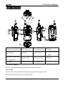


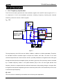

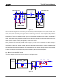
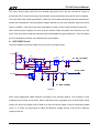
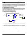
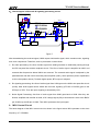


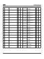

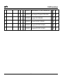
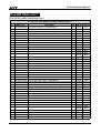
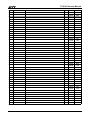


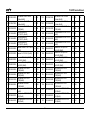


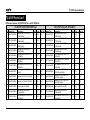
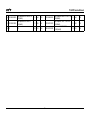

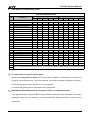

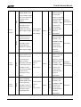
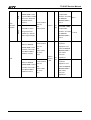
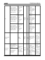


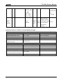
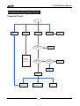


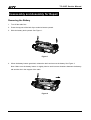


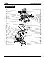


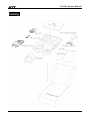
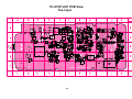
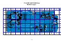


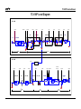
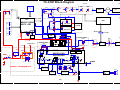

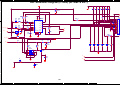


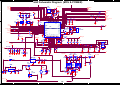

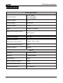


![[T3kCfg User Manual]](http://vs1.manualzilla.com/store/data/005811198_1-b56f11e7d0771a8aa23c614d4bbca2a5-150x150.png)