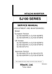
1
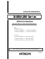
HITACHI INVERTER
SJ200/L200 Series
SERVICE MANUAL
(ADJUSTMENT AND MAINTENANCE)
Model:
European Version
SJ200/L200-002NFE(F) to SJ200/L200-022NFE(F)
SJ200/L200-004HFE(F) to SJ200/L200-075HFE(F)
US Version
SJ200/L200-002NFU to SJ200/L200-022NFU
SJ200/L200-037LFU to SJ200/L200-075LFU
SJ200/L200-004HFU to SJ200/L200-075HFU
After reading this manual, keep it at hand for future reference
NBS650X
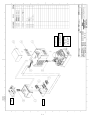
Appearance and name of each parts
SJ200-002 - 007LFR
SJ200-015 - 037LFR
SJ200-004 - 037HFR
potentiometer
digital operator
digital operator
front cover
potentiometer
front cover
top cover
top cover
housing
housing
cooling fin
cooling fin
rear cover
rear cover
ground
ground
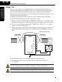
The front cover can be removed without any instruments. When you remove the front cover, you can
set the mode switch and set wire at the control-terminal, the main-terminal and the intelligent relay
output terminal.
control-terminal A
control-terminal A
(TM1C)
(TM1C)
control-terminal B
(TM2C)
control-terminal B
(TM2C)
upper cover
intelligent relay
output terminal
intelligent relay
output terminal
main terminal
main terminal
Note: The upper cover is for maintenance.
Please do not remove.
1-2
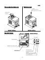
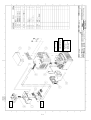
SJ200-055~075LFR
SJ200-055~075HFR
volume
digital operator
front cover
top cover
housing
rear cover
case
cooling fin
The front cover can be removed without any instruments When you remove the front cover, you can set
the mode switch and set wire at the control-terminal, the main-terminal and the intelligent relay output
terminal.
intelligent relay output terminal
control-terminal A
control-terminal B
main terminal
1-4
knob of potentiometer
Note:The knob can be taken.
digital operator
communication connector for operator
and RS-485
connector of
digital operator
POWER light
ALARM light
RUN light
control-terminal A
control-terminal B
intelligent relay output
terminal
input logic switch
main-terminal
turning switch RS-485/Operator
turning switch of frequency source and
run command source
1-3
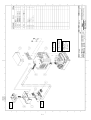
L200-002~007LFR
L200-015~037LFR
L200-004~037HFR
connector cover
volume
digital operator
digital operator
front cover
connector cover
volume
front cover
top cover
top cover
housing
housing
rear cover
cooling fin
rear cover
cooling fin
ground
ground
The front cover can be removed without any instruments. When you remove the front cover, you can set the mode
switch and set wire at the control-terminal, the main-terminal and the intelligent relay、output terminal.
control-terminal
control-terminal
intelligent relay
output terminal
upper cover
intelligent relay
output terminal
main terminal
main terminal
Note: The upper cover is for maintenance.
Please do not remove.
1-6
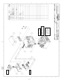
L200-055~075LFR
L200-055~075HFR
volume
digital operator
front cover
top cover
housing
rear cover
case
cooling fin
The front cover can be removed without any instruments. When you remove the front cover,
you can set the mode switch and set wire at the control-terminal, the main-terminal and the
intelligent relay output terminal.
intelligent relay output
terminal
control-terminal
main-terminal
1-7
(L200)
The way to open the connector cover
Removing the volume
volume
The volume can be removed
communication
connector
L200-002~007LFR type
L200-002~007LFR type
Items inside frontcover
L200-002~007LFR type
mode switch
control-terminal
intelligent relay output terminal
input logic switch
main terminal
turning switch RS-485/
Operator
turning switch frequency source/
run command source
1-8
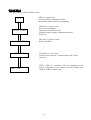
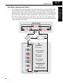
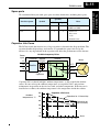
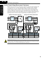
Appearance
The appearance of SJ200 follows below.
OPE
I/O PCB (PCB3)
Power PCB (PCB2)
Core PCB (PCB1)
IGBT / DM
OPE is a control unit.
Formally OPE is attached to SJ200.
But another OPE can be used optionally.
This part is a logic circuit.
It has a microcomputer,
which does calculation of the
intelligent input, output, communication task
and so on
This part is a power circuit.
It has a translator
This part is a core circuit.
It has a microcomputer , which manages INV main
function.
IGBT / DM. is a transistor unit for outputting to the
motor. It depends on the capacity and the voltage class
whether IGBT or DM is used.
1-4
1-1
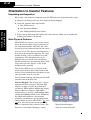
Introduction
Getting Started
Inverter Specifications Label
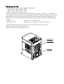
The Hitachi SJ200 inverters have product labels located on the right side of the housing,
as pictured below. Be sure to verify that the specifications on the labels match your
power source, motor, and application safety requirements.
Specifications label
Inverter model number
Motor capacity for this model
Power Input Rating:
frequency, voltage, phase, current
Output Rating:
Frequency, voltage, current
Manufacturing codes:
Lot number, date, etc.
Model Number Convention
The model number for a specific inverter contains useful information about its operating
characteristics. Refer to the model number legend below:
SJ200
037
H
F
E
F
EMC filter
Restricted distribution:
E=Europe, U=USA, R=Japan
Series name
Configuration type
F = with digital operator (keypad)
Input voltage:
N = single or three-phase 200V class
H = three-phase 400V class
L = three phase only, 200V class
Applicable motor capacity in kW
022 = 2.2 kW
002 = 0.2 kW
030 = 3.0 kW
004 = 0.4 kW
037 = 3.7 kW
005 = 0.55 kW
040 = 4.0 kW
007 = 0.75 kW
055 = 5.5 kW
011 = 1.1 kW
075 = 7.5 kW
015 = 1.5 kW
2–2
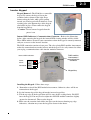
Orientation to Inverter Features
Orientation to Inverter Features
Unpacking and Inspection
Please take a few moments to unpack your new SJ200 inverter and perform these steps:
1. Look for any damage that may have occurred during shipping.
2. Verify the contents of the box include:
a. One SJ200 inverter
Inverter Mounting
and Installation
b. One Instruction Manual
c. One SJ200 Quick Reference Guide
3. Inspect the specifications label on the side of the inverter. Make sure it matches the
product part number you ordered.
Main Physical Features
The SJ200 Series inverters vary in size according to the current output rating and motor size
for each model number. All feature the same
basic keypad and connector interface for consistent ease of use. The inverter construction has a
heat sink at the back of the housing. The larger
models include a fan(s) to enhance heat sink
performance. The mounting holes are predrilled in the heat sink for your convenience.
Smaller models have two mounting holes, while
larger ones have four. Be sure to use all the
mounting holes provided.
Two chassis GND screws are located on the
metal tab on the heat sink at the bottom of the
inverter. Never touch the heat sink during or just
after operation; it can be very hot.
The electronics housing and front panel are built
onto the front of the heat sink.
Inverter Keypad - The inverter uses a digital
operator interface, or keypad. The four-digit
display can show a variety of performance
parameters. LEDs indicate whether the display
units are Hertz or Amperes. Other LEDs
indicate Power (external), and Run/Stop Mode
and Program/Monitor Mode status. Membrane
keys Run and Stop/Reset, and an output
frequency potentiometer (speed setting knob)
control motor operation. The FUNC., 1 , and
2 keys allow an operator to navigate to the
inverter’s functions and parameter values. The
Store key is used when changing a setting.
*Keypad doesn't display
when it is connected badly.
SJ200 Inverter
2–3
Inverter Keypad
Internal LED Indicators / Communications Connector - Refer to the illustration
below. After removing the keypad, the internal LED viewing window will be visible.
These LEDs indicate status for your convenience when the keypad is remotely mounted
and you are nearer to the inverter location.
The RJ45 connection consists of two parts. The clear plastic RJ45 modular interconnect
makes the connection between the inverter and the keypad. It is easily removed to allow
you to plug a communications cable into the modular connector.
Internal LED indicators:
Power
POW
Alarm
ALM
RJ45 modular
interconnect /
communications
connector
Run Mode RUN
Keypad bay
Installing the Keypad - Follow these steps:
1. Remember to install the RJ45 modular interconnect. Otherwise, there will be no
connection to the keypad.
2. Set the bottom edge of the keypad into the inverter keypad bay.
3. Tilt the top edge of the keypad forward. If it stops before seating firmly, DO NOT
force the keypad. You may need to adjust the end RJ45 modular connector slightly
(upward or downward). Then seat the keypad.
4. Make sure the retention latch clicks into place on the inverter housing top edge.
Otherwise, vibration may cause the keypad to loosen in the future.
Inverter Mounting
and Installation
Keypad Removal - The SJ200 has a removable
keypad. To remove the keypad, locate the
retention latch as shown to the right. Press
downward on the latch, while gently pulling
toward you. The keypad will tilt forward, as two
retaining tabs at the bottom edge of the keypad
also hold it in place. Then remove the keypad
from the keypad bay.
*Caution - Do not remove keypad when the
power is on.
2–4
Orientation to Inverter Features
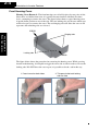
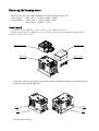
Front Housing Cover
Housing Cover Removal - The front housing cover is held in place by two pairs of tabs.
Since these are hidden from view, it is good to become familiar with their locations
before attempting to remove the cover. The figure below shows a typical housing cover
in upside-down position to reveal the tabs. The two locking tabs are the ones which you
will need to press to remove the cover. The two hinging tabs will allow the cover to tilt
open once the unlocking tabs are released.
PRESS
Inverter Mounting
and Installation
Hinging tabs
Locking tabs
PRESS
The figure below shows the procedure for removing the housing cover. While pressing
inward on the housing, it is helpful to wiggle the cover side-to-side in order to release the
locking tabs. DO NOT force the cover open; it is possible to break a tab in this way.
1. Press inward on both sides.
2. Tilt upward after both locking
tabs are free.
Removing the Cover (Slide type)
1. Press downward on the cover at the two areas indicated to release the retaining tabs.
2. Slide the cover forward and away from the keypad until the top edge of the cover reaches the notch in the
inverter chassis.
3. Lift the cover upward to remove it.
Installing the Cover (Slide type)
1. Align the tabs on the front housing cover with the notch on each edge of the inverter chassis. Then lower
the cover into position.
2. Slide the cover toward the keypad, keeping it flush against the inverter chassis. Continue until the cover
latches into place.
The notch on
front housing cover
The notch on frame case
Note: The example inverter in the diagrams is model L200-004LFU. The cover removal or installation method is the same for the other models.
WARNING: Be sure to turn off the power supply and wait 10 minutes before you remove the front housing
cover. Otherwise, there is a shock hazard.
SJ200 Inverter
2–5
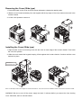
Logic Connector Locations - After removing the front housing cover, take a moment to
become familiar with the connectors, as shown below.
Relay output
contacts
Logic inputs
Logic Connector Removal/Replacement - The two 8-position main logic connectors
are removable from the circuit board to make testing or service more convenient. Note
that the relay output connector is not removable, as it must carry higher currents and
provide high integrity for alarm conditions. The alarm circuit may carry hazardous live
voltages even when the main power to the inverter is OFF. So, never directly touch any
terminal or circuit component.
The logic input connector (top connector) can be removed by pulling gently upward as
shown (below left). DO NOT force the connector, as damage to the circuit board may
occur. Try gently shifting the connector side-to-side while pulling, if having difficulty.
The analog input/output and logic output connector (bottom connector) has retention
screws. DO NOT attempt to remove the connector before loosening the screws. As the
figure shows (below right), use a small Phillips screwdriver to loosen the screw at each
end. The connector can be pulled forward easily after the screws are removed.
Inverter Mounting
and Installation
Analog input/
output and logic
outputs
2–6
Orientation to Inverter Features
Inverter Mounting
and Installation
Power Wiring Access - First, ensure no
power source of any kind is connected to the
inverter. If power has been connected, wait
five minutes after powerdown and verify the
Power LED is OFF to proceed. After
removing the front housing cover, the housing
partition that covers the power wiring exit will
be able to slide upward as shown to the right.
Notice the four wire exit slots (on larger
model inverters) in the housing partition. This
helps keep the power wiring (to the left)
separate from signal-level logic or analog
wiring (to the right).
Remove the housing partition and as shown as
set it aside in a secure place while wiring.
Never operate the inverter drive with the partition removed or the front housing cover
removed.
The power input and motor 3-phase wiring
connect to the lower row of terminals. The
upper row of power terminals connect to
optional dynamic braking components.
The following sections in this chapter will
describe the system design and guide you
through a step-by-step installation process.
After the section on wiring, this chapter
will show how to use the front panel keys
to access functions and edit parameters.
Power and motor
connector terminals
B–4
Connecting the Inverter to ModBus
OPE / 485 DIP Switch The difference between OPE-S and OPE-Smini is the short-circuit inside the connector.
If you set 485-side OPE-S,SRW says "----"(communication error)
But OPE-Smini works properly.
SR
485
TM
OPE
PRG
Appendix B
SK
C–2
Introduction
Introduction
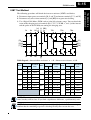
This section lists the user-programmable parameters for the SJ200 series inverters and
the default values for European and U.S. product types. The right-most column of the
tables is blank, so you can record values you have changed from the default. This
involves just a few parameters for most applications. This section presents the parameters in a format oriented toward the keypad on the inverter.
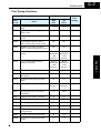
Parameter Settings for Keypad Entry
SJ200 series inverters provide many functions and parameters that can be configured by
the user. We recommend that you record all parameters that have been edited, in order to
help in troubleshooting or recovery from a loss of parameter data.
Inverter model
}
This information is printed
on the specification label
located on the right side of
the inverter.
SJ200
Appendix C
MFG. No.
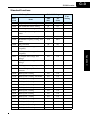
Main Profile Parameters
“F” Group Parameters
Func.
Code
Name
Default Setting
–FE
(Europe)
–FU
(USA)
F001
Output frequency setting
0.0
0.0
F002
Acceleration (1) time setting
10.0
10.0
F202
Acceleration (1) time setting, 2nd
motor
10.0
10.0
F003
Deceleration (1) time setting
10.0
10.0
F203
Deceleration (1) time setting, 2nd
motor
10.0
10.0
F004
Keypad Run key routing
00
00
User
Setting
SJ200 Inverter
C–3
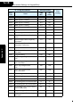
Standard Functions
“A” Group Parameters
Func.
Code
Name
Default Setting
-FEF
(EU)
-FU
(USA)
Frequency source setting
01
00
A002
Run command source setting
01
02
A003
Base frequency setting
50.0
60.0
A203
Base frequency setting, 2nd
motor
50.0
60.0
A004
Maximum frequency setting
50.0
60.0
A204
Maximum frequency setting, 2nd
motor
50.0
60.0
A005
[AT] selection
00
00
A011
O–L input active range start
frequency
0.0
0.0
A012
O–L input active range end
frequency
0.0
0.0
A013
O–L input active range start
voltage
0.0
0.0
A014
O–L input active range end
voltage
100.
100.
A015
O–L input start frequency enable
01
01
A016
External frequency filter time
constant
2.
8.
A020
Multi-speed 0 setting
0.0
0.0
A220
Multi-speed 0 setting, 2nd motor
0.0
0.0
A021
Multi-speed 1 setting
0.0
0.0
A022
Multi-speed 2 setting
0.0
0.0
A023
Multi-speed 3 setting
0.0
0.0
A024
Multi-speed 4 setting
0.0
0.0
A025
Multi-speed 5 setting
0.0
0.0
A026
Multi-speed 6 setting
0.0
0.0
A027
Multi-speed 7 setting
0.0
0.0
A028
Multi-speed 8 setting
0.0
0.0
A029
Multi-speed 9 setting
0.0
0.0
A030
Multi-speed 10 setting
0.0
0.0
A031
Multi-speed 11 setting
0.0
0.0
Appendix C
A001
User
Setting
C–4
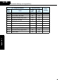
Parameter Settings for Keypad Entry
“A” Group Parameters
Appendix C
Func.
Code
Name
Default Setting
-FEF
(EU)
-FU
(USA)
A032
Multi-speed 12 setting
0.0
0.0
A033
Multi-speed 13 setting
0.0
0.0
A034
Multi-speed 14 setting
0.0
0.0
A035
Multi-speed 15 setting
0.0
0.0
A038
Jog frequency setting
1.00
1.00
A039
Jog stop mode
00
00
A042
Manual torque boost value
5.0
5.0
A242
Manual torque boost value, 2nd
motor
0.0
0.0
A043
Manual torque boost frequency
adjustment
3.0
3.0
A243
Manual torque boost frequency
adjustment, 2nd motor
0.0
0.0
A044
V/f characteristic curve selection
02
02
A244
V/f characteristic curve selection,
2nd motor
02
02
A045
V/f gain setting
100.
100.
A046
iSLV voltage compensation
gain
100
100
A246
iSLV voltage compensation
gain, 2nd motor
100
100
A047
iSLV slip compensation
gain
100
100
A247
iSLV slip compensation
gain, 2nd motor
100
100
A051
DC braking enable
00
00
A052
DC braking frequency setting
0.5
0.5
A053
DC braking wait time
0.0
0.0
A054
DC braking force for deceleration
0
0
A055
DC braking time for deceleration
0.0
0.0
A056
DC braking / edge or level detection for [DB] input
01
01
A061
Frequency upper limit setting
0.0
0.0
A261
Frequency upper limit setting,
2nd motor
0.0
0.0
User
Setting
SJ200 Inverter
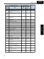
“A” Group Parameters
Func.
Code
Name
C–5
Default Setting
-FEF
(EU)
-FU
(USA)
Frequency lower limit setting
0.0
0.0
A262
Frequency lower limit setting,
2nd motor
0.0
0.0
A063,
A065,
A067
Jump (center) frequency setting
0.0
0.0
A064,
A066,
A068
Jump (hysteresis) frequency
width setting
0.5
0.5
A071
PID Enable
00
00
A072
PID proportional gain
1.0
1.0
A073
PID integral time constant
1.0
1.0
A074
PID derivative time constant
0.0
0.0
A075
PV scale conversion
1.00
1.00
A076
PV source setting
00
00
A077
Reverse PID action
00
00
A078
PID output limit
0.0
0.0
A081
AVR function select
00
00
A082
AVR voltage select
230/400
230/460
A092
Acceleration (2) time settin
15.00
15.00
A292
Acceleration (2) time setting,
(2nd motor)
15.00
15.00
A093
Deceleration (2) time setting
15.00
15.00
A293
Deceleration (2) time setting,
(2nd motor)
15.00
15.00
A094
Select method to switch to Acc2/
Dec2 profile
00
00
A294
Select method to switch to Acc2/
Dec2 profile, 2nd motor
00
00
A095
Acc1 to Acc2 frequency transition point
0.0
0.0
A295
Acc1 to Acc2 frequency transition point, 2nd motor
0.0
0.0
A096
Dec1 to Dec2 frequency transition point
0.0
0.0
Appendix C
A062
User
Setting
C–6
Parameter Settings for Keypad Entry
“A” Group Parameters
Appendix C
Func.
Code
Name
Default Setting
-FEF
(EU)
-FU
(USA)
A296
Dec1 to Dec2 frequency transition point, 2nd motor
0.0
0.0
A097
Acceleration curve selection
00
00
A098
Deceleration curve selection
00
00
A101
[OI]–[L] input active range start
frequency
0.0
0.0
A102
[OI]–[L] input active range end
frequency
0.0
0.0
A103
[OI]–[L] input active range start
current
0.0
0.0
A104
[OI]–[L] input active range end
current
100.
100.
A105
[OI]–[L] input start frequency
enable
01
01
A141
A input select for calculate
function
02
02
A142
B input select for calculate
function
03
03
A143
Calculation symbol
00
00
A145
ADD frequency
0.0
0.0
A146
ADD direction select
00
00
User
Setting
SJ200 Inverter
C–7
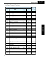
Fine Tuning Functions
“B” Group Parameters
Func.
Code
Name
Default Setting
-FEF
(EU)
-FU
(USA)
Selection of automatic restart
mode
00
00
B002
Allowable under-voltage power
failure time
1.0
1.0
B003
Retry wait time before motor
restart
1.0
1.0
B004
Instantaneous power failure /
under-voltage trip alarm enable
00
00
B005
Number of restarts on power
failure / under-voltage trip events
00
00
B012
Level of electronic thermal
setting
Rated
current for
each
inverter
Rated
current for
each
inverter
B212
Level of electronic thermal
setting, 2nd motor
Rated
current for
each
inverter
Rated
current for
each
inverter
B013
Electronic thermal characteristic
01
01
B213
Electronic thermal characteristic,
2nd motor
01
01
B021
Overload restriction operation
mode
01
01
B022
Overload restriction setting
Rated
current x
1.5
Rated
current x
1.5
B023
Deceleration rate at overload
restriction
1.0
30.0
B031
Software lock mode selection
01
01
B080
[AM] analog signal gain
100.
100.
B082
Start frequency adjustment
0.5
0.5
B083
Carrier frequency setting
5.0
5.0
B084
Initialization mode (parameters
or trip history)
00
00
B085
Country code for initialization
01
02
B086
Frequency scaling conversion
factor
1.0
1.0
Appendix C
B001
User
Setting
C–8
Parameter Settings for Keypad Entry
“B” Group Parameters
Appendix C
Func.
Code
Name
Default Setting
-FEF
(EU)
-FU
(USA)
B087
STOP key enable
00
00
B088
Restart mode after FRS
00
00
B090
Dynamic braking usage ratio
0.0
0.0
B091
Stop mode selection
00
00
B092
Cooling fan control
00
00
B095
Dynamic braking control
00
00
B096
Dynamic braking activation level
360/720
360/720
B130
Over-voltage LADSTOP enable
00
00
B140
Over-current trip suppression
00
00
B150
Carrier mode
00
00
User
Setting
SJ200 Inverter
C–9
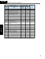
Intelligent Terminal Functions
“C” Group Parameters
Func.
Code
Name
Default Setting
-FEF
(EU)
-FU
(USA)
Terminal [1] function
00
00
C002
Terminal [2] function
01
01
C003
Terminal [3] function
02
16
C004
Terminal [4] function
03
13
C005
Terminal [5] function
18
09
C006
Terminal [6] function
09
18
C011
Terminal [1] active state
00
00
C012
Terminal [2] active state
00
00
C013
Terminal [3] active state
00
00
C014
Terminal [4] active state
00
01
C015
Terminal [5] active state
00
00
C016
Terminal [6] active state
00
00
C021
Terminal [11] function
01
01
C022
Terminal [12] function
00
00
C026
Alarm relay terminal function
05
05
C028
[AM] signal selection
00
00
C031
Terminal [11] active state
00
00
C032
Terminal [12] active state
00
00
C036
Alarm relay active state
01
01
C041
Overload level setting
Inverter
rated
current
Inverter
rated
current
C042
Frequency arrival setting for
acceleration
0.0
0.0
C043
Arrival frequency setting for
deceleration
0.0
0.0
C044
PID deviation level setting
3.0
3.0
C052
PID FBV function high limit
100.0
100.0
C053
PID FBV function low limit
0.0
0.0
C071
Communication speed selection
06
04
C072
Node allocation
1.
1.
C074
Communication parity selection
00
00
Appendix C
C001
User
Setting
C–10
Parameter Settings for Keypad Entry
Appendix C
“C” Group Parameters
Func.
Code
Default Setting
Name
-FEF
(EU)
-FU
(USA)
C075
Communication stop bit selection
1
1
C076
Communication error select
02
02
C077
Communication erorr time-out
0.00
0.00
C078
Communication wait time
0.
0.
C081
O input span calibration
100.0
100.0
C082
OI input span calibration
100.0
100.0
C085
Thermistor input tuning
100.0
100.0
C086
[AM] terminal offset tuning
0.0
0.0
C091
Debug mode enable
00
00
C101
Up/Down memory mode
selection
00
00
C102
Reset selection
00
00
C141
Input A select for logic output
00
00
C142
Input B select for logic output
01
01
C143
Logic function select
00
00
C144
Terminal [11] ON delay
0.0
0.0
C145
Terminal [11] OFF delay
0.0
0.0
C146
Terminal [12] ON delay
0.0
0.0
C147
Terminal [12] OFF delay
0.0
0.0
C148
Output relay ON delay
0.0
0.0
C149
Output relay OFF delay
0.0
0.0
User
Setting
SJ200 Inverter
C–11
Motor Constants Functions
“H” Group Parameters
Func.
Code
Name
Default Setting
-FEF
(EU)
-FU
(USA)
Motor capacity
Specified
by the
inverter
capacity
Specified
by the
inverter
capacity
H203
Motor capacity, 2nd setting
Specified
by the
inverter
capacity
Specified
by the
inverter
capacity
H004
Motor poles setting
4
4
H204
Motor poles setting, 2nd motor
4
4
H006
Motor stabilization constant
100
100
H206
Motor stabilization constant, 2nd
motor
100
100
H007
Motor voltage select
Specified
by the
inverter
voltage
Specified
by the
inverter
voltage
H207
Motor voltage select, 2nd motor
Specified
by the
inverter
voltage
Specified
by the
inverter
voltage
Appendix C
H003
User
Setting
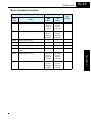
Troubleshooting
and Maintenance
6–2
Troubleshooting
Troubleshooting
Safety Messages
Please read the following safety messages before troubleshooting or performing maintenance on the inverter and motor system.
WARNING: Wait at least five (5) minutes after turning OFF the input power supply
before performing maintenance or an inspection. Otherwise, there is the danger of
electric shock.
WARNING: Make sure that only qualified personnel will perform maintenance, inspection, and part replacement. Before starting to work, remove any metallic objects from
your person (wristwatch, bracelet, etc.). Be sure to use tools with insulated handles.
Otherwise, there is a danger of electric shock and/or injury to personnel.
WARNING: Never remove connectors by pulling on its wire leads (wires for cooling
fan and logic P.C.board). Otherwise, there is a danger of fire due to wire breakage and/or
injury to personnel.
General Precautions and Notes
• Always keep the unit clean so that dust or other foreign matter does not enter the
inverter.
• Take special care in regard to breaking wires or making connection mistakes.
• Firmly connect terminals and connectors.
• Keep electronic equipment away from moisture and oil. Dust, steel filings and other
foreign matter can damage insulation, causing unexpected accidents, so take special
care.
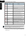
Inspection Items
This chapter provides instructions or checklists for these inspection items:
• Daily inspection
• Periodic inspection (approximately once a year)
• Insulation resistance test
SJ200 Inverter
6–3
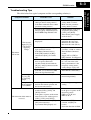
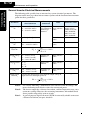
Troubleshooting Tips
Symptom/condition
Probable Cause
• Is the frequency command source
Solution
• Make sure the parameter
A001 parameter setting correct?
setting A001 is correct.
• Is the Run command source A002
• Make sure the parameter
parameter setting correct?
• Is power being supplied to terminals [L1], [L2], and [L3/N]? If so,
the POWER lamp should be ON.
• Is there an error code E X X
displayed?
The inverter
outputs [U], [V],
[W] are not
• Are the signals to the intelligent
supplying
input terminals correct?
voltage.
• Is the Run Command active?
The motor
• Is the [FW] terminal (or [RV])
will not run.
connected to [P24] (via switch,
etc.)
• Has the frequency setting for F001
been set greater than zero?
• Are the control circuit terminals
[H], [O], and [L] connected to the
potentiometer?
• Is the RS (reset) function or FRS
setting A002 is correct.
• Check terminals [L1], [L2],
and [L3/N], then [U/T1],
[V/T2], and [W/T3].
• Turn ON the power supply
or check fuses.
• Press the Func. key and
determine the error type.
Eliminate the error cause,
then clear the error (Reset).
• Verify the terminal functions
for C001 – C006 are correct.
• Turn ON Run Command
enable.
• Supply 24V to {FW] or
[RV] terminal, if configured.
• Set the parameter for F001
to a safe, non-zero value.
• If the potentiometer is the
frequency setting source,
verify voltage at [O] > 0V.
• Turn OFF the command(s).
(free-run stop) function ON?
Inverter outputs
[U], [V], [W]
are supplying
voltage.
• Is the motor load too heavy?
The optional
remote operator
is used (SRW).
• Are the operational settings
motor independently.
between the remote operator and
the inverter unit correct?
• Are the connections of output
The direction of the motor is
reversed.
• Reduce load, and test the
terminals [U/T1], [V/T2], and
[W/T3] correct?
• Is the phase sequence of the motor
forward or reverse with respect to
[U/T1], [V/T2], and [W/T3]?
• Check the operator type
setting.
• Make connections according
to the phase sequence of the
motor. In general:
FWD = U-V-W, and
REV=U-W-V.
• Are the control terminals [FW] and • Use terminal [FW] for
[RV] wired correctly?
• Is parameter F004 properly set?
forward, and [RV] for
reverse.
• Set motor direction in F004.
Troubleshooting
and Maintenance
The table below lists typical symptoms and the corresponding solution(s).
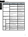
6–4
Troubleshooting
Troubleshooting
and Maintenance
Symptom/condition
Probable Cause
• If using the analog input, is the
current or voltage at [O] or [OI]?
Solution
• Check the wiring.
• Check the potentiometer or
signal generating device.
• Is the load too heavy?
The motor speed will not reach
the target frequency (desired
speed).
overload restriction feature
(reduces output as needed).
• Is the inverter internally limiting
the output frequency?
• Is the load fluctuation too great?
The rotation is unstable.
• Was power turned OFF after a
Inverter data
is not
correct.
A parameter
will not
change after
an edit
(reverts to
old setting).
• Check max frequency
setting (A004)
• Check frequency upper limit
setting (A061)
• Increase the motor capacity
(both inverter and motor).
• Is the supply voltage unstable?
• Fix power supply problem.
• Is the problem occurring at a partic- • Change the output
ular frequency?
frequency slightly, or use the
jump frequency setting to
skip the problem frequency.
The RPM of the motor does not • Is the maximum frequency setting
match the inverter output
A004 correct?
frequency setting.
• Does the monitor function D001
display the expected output
frequency?
No downloads
have occurred.
• Reduce the load.
• Heavy loads activate the
parameter edit but before pressing
the Store key?
• Edits to data are permanently
stored at power down. Was the time
from power OFF to power ON less
than six seconds?
• Verify the V/f settings match
motor specifications.
• Make sure all scaling (such
as A011 to A014) is
properly set.
• Edit the data and press the
Store key once.
• Wait six seconds or more
before turning power OFF
after editing data.
A download to
the inverter was
attempted.
• Was the power turned OFF within
True for certain
parameters
• Is the inverter in Run Mode? Some • Put inverter in Stop Mode
True for all
parameters
• If you’re using the [SFT] intelligent • Change the state of the SFT
six seconds after the display
changed from REMT to INV?
parameters cannot be edited during
Run Mode.
input (software lock function)—is
the [SFT] input ON?
• Copy the data to the inverter
again, and keep power ON
for six seconds or more after
copying.
(press the Stop/reset key).
Then edit the parameter.
input, and check the B031
parameter (SFT mode).
SJ200 Inverter
6–5
Fault Detection and Clearing
The microprocessor in the inverter detects a variety
STOP
RESET
of fault conditions and captures the event, recordRun
Stop
ing it in a history table. The inverter output turns
RUN
OFF, or “trips” similar to the way a circuit breaker
STOP
trips due to an over-current condition. Most faults
RESET
Fault
occur when the motor is running (refer to the
Trip
Fault
diagram to the right). However, the inverter could
have an internal fault and trip in Stop Mode. In
either case, you can clear the fault by pressing the Stop/Reset key. Additionally, you can
clear the inverter’s cumulative trip history by performing the procedure “Restoring
Factory Default Settings” on page 6–8 (setting B084=00 will clear the trip history but
leave inverter settings intact).
Error Codes
An error code will appear on the display automatically when a fault causes the inverter to
trip. The following table lists the cause associated with the error.
Error
Code
E 01
E 02
E 03
E 04
Name
Over current event while
at constant speed
Over current event during
deceleration
Over current event during
acceleration
Cause(s)
The inverter output was short-circuited, or the motor
shaft is locked or has a heavy load. These conditions
cause excessive current for the inverter, so the
inverter output is turned OFF.
The dual-voltage motor is wired incorrectly.
If b083 is too high, please reduce the value.
Over current event during
other conditions
E 05
Overload protection
When a motor overload is detected by the electronic
thermal function, the inverter trips and turns OFF its
output.
E 06
Braking resistor overload
When the regenerative braking resistor exceeds the
usage time allowance or usage ratio, the inverter trips
and turns OFF its output to the motor.
E 07
Over voltage protection
When the DC bus voltage exceeds a threshold, due to
regenerative energy from the motor.
E 08
EEPROM error
When the built-in EEPROM memory has problems
due to noise or excessive temperature, the inverter
trips and turns OFF its output to the motor.
E 09
Under-voltage error
A decrease of internal DC bus voltage below a threshold results in a control circuit fault. This condition can
also generate excessive motor heat or cause low
torque. The inverter trips and turns OFF its output.
Troubleshooting
and Maintenance
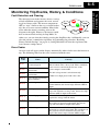
Monitoring Trip Events, History, & Conditions
Troubleshooting
and Maintenance
6–6
Monitoring Trip Events, History, & Conditions
Error
Code
E1 1
E22
E1 2
Name
Cause(s)
CPU error
A malfunction in the built-in CPU has occurred, so
the inverter trips and turns OFF its output to the
motor.
External trip
A signal on an intelligent input terminal configured as
EXT has occurred. The inverter trips and turns OFF
the output to the motor.
E1 3
USP
When the Unattended Start Protection (USP) is
enabled, an error occurred when power is applied
while a Run signal is present. The inverter trips and
does not go into Run Mode until the error is cleared.
E1 4
Ground fault
The inverter is protected by the detection of ground
faults between the inverter output and the motor upon
during powerup tests. This feature protects the
inverter, and does not protect humans.
Input over-voltage
(*)
When the input voltage is higher than the specified
value, it is detected 100 seconds after powerup and
the inverter trips and turns OFF its output.
E21
Inverter thermal trip
When the inverter internal temperature is above the
threshold, the thermal sensor in the inverter module
detects the excessive temperature of the power
devices and trips, turning the inverter output OFF.
E23
Gate array error
An internal inverter error has occurred in communications between the CPU and gate array IC.
E35
Thermistor
When a thermistor is connected to terminals [6] and
[L] and the inverter has sensed the temperature is too
high, the inverter trips and turns OFF the output.
E 60
Communications error
The inverter’s watchdog timer for the communications network has timed out.
Under-voltage (brownout) with output shutoff
Due to low input voltage, the inverter turns its output
OFF and tries to restart. If it fails to restart, then the
alarm trips to record the under-voltage error event.
E1 5
---
NOTE: If an EEPROM error (E08) occurs, be sure to confirm the parameter data values
are still correct. If the power is turned OFF while the [RS] (Reset) intelligent input
terminal is ON, an EEPROM error will occur when power is restored.
Caution: EXT,PTC trip has a possibility of breaking I/O circuit and breaking EEPROM data
*:OVSRC(E15) trip level is relatively changed for 200/400V class in 3440(Core) and
3524(I/O) software.
SJ200 Inverter
6–7
Trip History and Inverter Status
The following Monitor Menu map shows how to access the error codes. When fault(s)
exist, you can review their details by first selecting the proper function: D081 is the most
recent, and D083 is the oldest.
Monitor Menu
2
2
d 083
2
1
d 081
1
d 082
FUNC.
No error
Error
exists?
____
No
FUNC.
Yes
2
E 09
1
DC bus voltage
at trip point
2
15
1
Motor current
at trip point
2
1 8 9.8
1
Output frequency
at trip point
2
0.25
1
Error Code
2
1 0.0
1
Trip
Conditions
2
18
Cumulative inverter
operation time at
trip point
Cumulative powerON time at trip point
1
FUNC.
2
Troubleshooting
and Maintenance
We recommend that you first find the cause of the fault before clearing it. When a fault
occurs, the inverter stores important performance data at the moment of the fault. To
access the data, use the monitor functions (Dxxx) and select D081 for details about the
present fault (En). The previous two faults are stored in D082 and D083, with D(En-1 and
En-2). Each error shifts D081–D082 to D082–D083, and writes the new error to D081.
Troubleshooting
and Maintenance
6–8
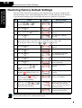
Restoring Factory Default Settings
Restoring Factory Default Settings
You can restore all inverter parameters to the original factory (default) settings for the
intended country of use. After initializing the inverter, use the powerup test in Chapter 2
to get the motor running again. To initialize the inverter, follow the steps below.
No.
Action
Display
Func./Parameter
b–––
“B” Group selected
b 001
First “B” parameter selected
b 085
Country code for initialization
selected
1
Use the FUNC. , 1 , and 2 keys to
navigate to the “B” Group.
2
Press the
3
Press and hold the
4
Press the
5
Confirm the country code is correct. Do not change it unless you are absolutely sure the
power input voltage range and frequency match the country code setting.
FUNC.
FUNC.
key.
1
key until ->
02
key.
To change the country code, press
1
or
2
to set,
00 = Japan, 01 = Europe,
02 = U.S.
STR
to store.
6
Press the
FUNC.
key.
b 085
Country code for initialization
selected
7
Press the
2
key.
b 084
Initialization function selected
8
Press the
FUNC.
key.
00
00 = initialization disabled,
clear trip history only
9
Press the
1
key.
01
01 = initialization enabled
10
Press the
STR
key.
11
Press and hold the
2
12
,
1
, and
Initialization now enabled to
restore all defaults
b 084
First part of special key
sequence
b 084
Final part of special key
sequence
d 001
Initialization begins when
display starts blinking
keys. Do not release yet.
Holding the keys above, press and
hold the
13
FUNC.
b 084
STOP
RESET
(STOP) key for 3 sec.
STOP
Release only the RESET
(STOP) key,
and wait for the display d001 to
appear and begin blinking.
14
, and 2
keys only after the d001 display
function begins blinking.
15
Initialization is complete.
Now release the
FUNC.
,
1
EU
USA
d 001
Default parameter country code
shown during initialization
process (left-most char displays
alternating pattern)
Function code for output
frequency monitor shown
NOTE: Initialization cannot be performed with a remote operator panel. Disconnect the
device and use the inverter’s front panel keypad.
EEPROM Compulsory Initialization
All of EEPROM data are stored default setting
-method1. After setting C091=01, store ‘**FF’ at EEPROM address 11d4(C092 setting).
2. Then press and hold the FUNC, UP, and DOWN key.
HITACHI
POWER
ALARM
Hz
A
RUN
FUNC
RUN
PRG
STOP
RESET
1
2
STR
3. After that press RESET key and release.
4. Then INV starts compulsory initialization as it displays like below.
Now
initialization
At the left side the bars blink and roll
5. EEPROM compulsory initialization completes.
6. Set Voltage-class (C197),and set C195,b085(both must be the same.)
7. Set INV kW Code (C196) the wrong value once intentionally
and store, then set the right value. After that start initialization with b084
-C081,C082O-L adjustment at factory(not C81, not C82)
JPN version is 1 byte definition
Core:up to 3388(or before)
IO:up to 3433(or before)
EU/USA version is 2 byte definition from the beginning.
Core: 3440 or after
IO: 3441 or after
When initialization of b084 or copying C081 and C082 are set different value, so need to set
again.
2-1
ERROR Check
error
No display
E08/E11
E22
8888 display
OC trip/E23/
E30/E14
---(Power Off
display)
E09 with
motor
E12(EXT)
E35(PTC)
E05(Over
Load),OC
trip(L200)is prematured
Cooling FAN doesn't
work
INV doesn't work
MOV failure, or you got
returned INV
bar-bar-bar-bar
display(OPE-S,OPE-SRE,
not OPE-Smini)
or
R-ERROR
COMM.<1>(SRW)
No display
description
DC bus charged
IO board connection & cable connection
OPE connection
short bar P1- PD
Cooling FAN failure
Connection between IO board & OPE(L200)
EEPROM recovery(initilalization C92 display 11d4=ff)
IO board connection & cable connection(communication error
between ISPM & IO board)
INV type code is wrong SJ200 & L200
EEPROM
recovery(initilalization
C92
11d4=ff)(because MCU can't read EEPROM)
EEPROM data changed. check C194
Disconnect motor wire and check output voltage
display
Core(ISPM) failure(not repairable)
maybe thyristor off, please check waveform of DC bus voltage.
check C01-C06 (EXT=12)
check C06(SJ200)-C05(L200)(PTC=19) ,check C85 value
check b32 value
check b92
check DIP switch on ISPM(Power Module pcb)
check d109 display after C91 set 01
Set dip Switch from 485 to PRG
check the bar of P-line.
2-2
Debug Mode
If you set debug mode enable (C091 =01), the function below will be available.
When debugging, you can use only standard OPE (cannot use SRW)
Make sure of returning C091=00 after debugging.
There are some monitor or function-code for testing and maintenance which is not released for
users.
The content of each function follows below.
Monitor mode
No
1
2
3
4
5
6
7
Function name
Control-frequenc
y monitor
DC voltage
monitor
BRD ON time
monitor
Electric thermal
monitor
Core MCU NO.
IO MCU NO.
Peak voltage
monitor
Code
Run
Mode
Edit
Range
d101
-
0.0~400.0
d102
-
d103
Res.
defa
ult
unit
Monitors control frequency
0.1[Hz]
-
Hz
0.0~999.9
Monitors the P-N voltage
0.1[V]
-
V
-
0.0~100.0
Monitors the time during BRD ON
0.1[sec]
-
%
d104
-
0.0~100.0
0.1%
-
-
d106
-
0000~9999
1
-
-
d107
-
0000~9999
1
-
-
d109
-
0.0~999.9
0.1[V]
-
V
Description
Monitors integration of the current
when exceeding the thermal level.
Monitors the version of
the core program
Monitors the version of
the IO program
Monitors the peak P-N voltage
Function mode
No
Function name
Code
Run
Mode
Edit
Range
Description
Res.
defa
ult
unit
8
Debug mode
enable
C091
OK
00(disable)/
01(enable)
Debug mode select
-
00
-
9
Debug mode
data set
C092
OK
0000~FFFF
Hexadecimal display
(Do not set)
-
1200
-
10
Debug mode
data monitor
C093
OK
0000~FFFF
Hexadecimal display
(Do not set)
-
1200
-
11
Debug mode
bit control
C094
OK
Address set range
0000 - FFFF->
0-7 bit select
Hexadecimal display
(Do not set)
-
1200
-
12
Debug mode select
C095
OK
00(Core)/01(IO)
-
00
-
C121
-
0000~FFFF
Hexadecimal display
(Do not set)
-
3E8
-
C122
-
0000~FFFF
Hexadecimal display
(Do not set)
-
3E8
-
C123
-
0~65535
-
200
-
Area code select
-
-
-
Capacity select
Voltage-class
select
-
-
-
-
-
-
13
14
15
O input span
calibration
for function test
OI input span
calibration
for function test
OI Zero
calibration
for function test
(Do not set)
16
Area code select
C195
-
17
kW code
Voltage-class
select
C196
-
00(JPN)/01(EU)
/02(USA)
0.2~7.5
C197
-
00(200V)/01(400V)
18
Doesn’t store to
EEPROM
3-1
SJ200 Inverter
6–9
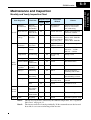
Monthly and Yearly Inspection Chart
Inspection Cycle
Item Inspected
Check for...
Month
Control
circuit
Criteria
Ambient
environment
Extreme
temperatures
& humidity
✔
Thermometer,
hygrometer
Ambient temperature
between -10 to 40°C,
non-condensing
Major devices
Abnormal
noise & vib.
✔
Visual and aural
Stable environment for
electronic controls
Power supply
voltage
Voltage
tolerance
✔
Digital volt meter,
measure between
inverter terminals
[L1], [L2], [L3]
200V class:
200 to 240V 50/60 Hz
400V class:
380 to 460V 50/60 Hz
Ground
Insulation
Adequate
resistance
✔
Digital volt meter,
GND to terminals
5 Meg. Ohms or greater
Mounting
No loose
screws
✔
Torque wrench
M3: 0.5 – 0.6 Nm
M4: 0.98 – 1.3 Nm
M5: 1.5 – 2.0 Nm
Components
Overheating
✔
Thermal trip
events
No trip events
Housing
Dirt, dust
✔
Visual
Vacuum dust and dirt
✔
Visual
No abnormalities
Visual
No abnormalities
Overall
Main
circuit
Year
Inspection
Method
Terminal block Secure
connections
✔
Smoothing
capacitor
Leaking,
swelling
Relay(s)
Chattering
✔
Aural
Single click when
switching ON or OFF
Resistors
Cracks or
discoloring
✔
Visual
Use Ohm meter to
check braking resistors
Cooling fan
Noise
✔
Power down,
manually rotate
Rotation must be
smooth
Dust
✔
Visual
Vacuum to clean
Visual
No abnormalities
✔
Overall
No odor,
discoloring,
corrosion
Capacitor
No leaks or
deformation
✔
Visual
Undistorted appearance
Legibility
✔
Visual
All LED segments work
Display LEDs
Note 1:
Note 2:
The life of a capacitor is affected by the ambient temperature. See “Capacitor
Life Curve” on page 6–11.
The inverter must be cleaned periodically. If dust accumulates on the fan and
heat sink, it can cause overheating of the inverter.
Troubleshooting
and Maintenance
Maintenance and Inspection
6–10
Maintenance and Inspection
Troubleshooting
and Maintenance
Megger Test
The megger is a piece of test equipment that uses a high voltage to determine if an
insulation degradation has occurred. For inverters, it is important that the power terminals be isolated from the Earth GND terminal via the proper amount of insulation.
The circuit diagram below shows the inverter wiring for performing the megger test. Just
follow the steps to perform the test:
1. Remove power from the inverter and wait at least 5 minutes before proceeding.
2. Open the front housing panel to access the power wiring.
3. Remove all wires to terminals [R, S, T, RB, PD/+1, PD/+, N/–, U, V, and W]. Most
importantly, the input power and motor wires will be disconnected from the inverter.
4. Use a bare wire and short terminals [R, S, T, RB, PD/+1, PD/+, N/–, U, V, and W]
together as shown in the diagram.
5. Connect the megger to the inverter Earth GND and to the shorted power terminals as
shown. Then perform the megger test at 500 VDC and verify 5MΩ or greater resistance.
Add test jumper wire
Disconnect
power source
Disconnect
motor wires
SJ200
R
U
S
V
T
W
RB
Motor
Megger, 500VDC
PD/+1
PD/+
N/–
Earth GND
6. After completing the test, disconnect the megger from the inverter.
7. Reconnect the original wires to terminals [R, S, T, RB, PD/+1, PD/+, N/–,
U, V, and W].
CAUTION: Do not connect the megger to any control circuit terminals such as intelligent I/O, analog terminals, etc. Doing so could cause damage to the inverter.
CAUTION: Never test the withstand voltage (HIPOT) on the inverter. The inverter has a
surge protector between the main circuit terminals above and the chassis ground.
SJ200 Inverter
6–11
Spare parts
Quantity
Part description
Symbol
Notes
Used
Spare
Cooling fan
FAN
1
1
015NF, 022NF, 030LF,
015HF to 075HF
Case
CV
1
1
•
•
•
•
Front case
Key cover
Case
Bottom cover
Capacitor Life Curve
The DC bus inside the inverter uses a large capacitor as shown in the diagram below. The
capacitor handles high voltage and current as it smooths the power for use by the
inverter. So, any degradation of the capacitor will affect the performance of the inverter.
Power
Input
Variable-frequency Drive
Converter
L1
L2
Internal
DC Bus
Inverter
Motor
+
+
Rectifier
U/T1
V/T2
L3
W/T3
–
Capacitor
Capacitor life is reduced in higher ambient temperatures, as the graph below demonstrates. Be sure to keep the ambient temperature at acceptable levels, and perform
maintenance inspections on the fan, heat sink, and other components. If the inverter is
installed on a cabinet, the ambient temperature is the temperature inside the cabinet.
Capacitor Life Curve
50
Ambient
temperature, °C
Operation for 12 hours/day
40
30
Operation for
24 hours/day
20
10
0
-10
1
2
3
4
5
6
7
8
9
10
Years
Troubleshooting
and Maintenance
We recommend that you stock spare parts to reduce down time, including these parts:
6–12
Maintenance and Inspection
Troubleshooting
and Maintenance
General Inverter Electrical Measurements
The following table specifies how to measure key system electrical parameters. The
diagrams on the next page show inverter-motor systems and the location of measurement
points for these parameters.
Parameter
Circuit location
of measurement
Measuring
instrument
Notes
Reference Value
Supply voltage
E1
ER – across L1 and L2
ES – across L2 and L3
ET – across L3 and L1
Moving-coil
Fundamental
type voltmeter or wave effective
rectifier type
value
voltmeter
Supply current
I1
Ir – L1, Is – L2, It – L3
Total effective
value
—
Supply power
W1
W11 – across L1 and L2
W12 – across L2 and L3
Total effective
value
—
Supply power
factor Pf1
Commercial
supply voltage
(200V class) 200–
240V, 50/60 Hz
400V class 380–
460V, 50/60 Hz
—
W1
Pf 1 = ------------------------------ × 100%
3 × E1 × I1
Output voltage
E0
EU – across U and V
EV – across V and W
EW – across W and U
Rectifier type
voltmeter
Total effective
value
—
Output current
Io
IU – U
IV – V
IW – W
Moving-coil
ammeter
Total effective
value
—
Output power
Wo
W01 – across U and V
W02 – across V and W
Electronic type
wattmeter
Total effective
value
—
Output power
factor Pfo
Calculate the output power factor from the output voltage E,
output current I, and output power W.
—
W0
Pf 0 = ------------------------------ × 100%
3 × E0 × I0
Note 1:
Note 2:
Note 3:
Use a meter indicating a fundamental wave effective value for voltage, and
meters indicating total effective values for current and power.
The inverter output has a distorted waveform, and low frequencies may cause
erroneous readings. However, the measuring instruments and methods listed
above provide comparably accurate results.
A general-purpose digital volt meter (DVM) is not usually suitable to measure
a distorted waveform (not pure sinusoid).
SJ200 Inverter
6–13
Single-phase Measurement Diagram
Inverter
L1
L1
I1
U
T1
I1
EU-V
E1
W1
V
T2
I1
EU-V
N
N
W
W01
Motor
W02
T3
I1
EU-V
Three-phase Measurement Diagram
Inverter
L1
R
I1
E1
L2
L3
EU-V
S
E1
V
T2
EU-V
W
W01
I1
W02
T
I3
T1
I1
W01
I2
E1
U
W02
T3
I1
EU-V
Motor
Troubleshooting
and Maintenance
The figures below show measurement locations for voltage, current, and power measurements listed in the table on the previous page. The voltage to be measured is the fundamental wave effective voltage. The power to be measured is the total effective power.
6–14
Maintenance and Inspection
Troubleshooting
and Maintenance
Inverter Output Voltage Measurement Techniques
Taking voltage measurements around drives equipment requires the right equipment and
a safe approach. You are working with high voltages and high-frequency switching
waveforms that are not pure sinusoids. Digital voltmeters will not usually produce
reliable readings for these waveforms. And, it is usually risky to connect high voltage
signals to oscilloscopes. The inverter output semiconductors have some leakage, and
no-load measurements produce misleading results. So, we highly recommend using the
following circuits to measure voltage for performing the equipment inspections.
Voltage measurement with load
L1/R
L2/S
U/T1
Inverter
L3/T
Voltage measurement without load
L1/R
V/T2
L2/S
W/T3
L3/T
U/T1
Inverter
V/T2
W/T3
Additional resistor
220 kΩ
2W
220 kΩ
2W
+
V Class
Diode Bridge
5 kΩ
30W
–
Voltmeter
+
V Class
Diode Bridge
–
Voltmeter
200V Class
600V 0.01A min. 300V range
200V Class
600V 0.01A min. 300V range
400V Class
100V 0.1A min.
400V Class
100V 0.1A min.
600V range
600V range
HIGH VOLTAGE: Be careful not to touch wiring or connector terminals when working
with the inverters and taking measurements. Be sure to place the measurement circuitry
components above in an insulated housing before using them.
6–15
SJ200 Inverter
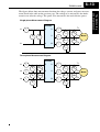
IGBT Test Method
1. Disconnect input power to terminals [R, S, and T] and motor terminals [U, V, and W].
2. Disconnect any wires from terminals [+] and [RB] for regenerative braking.
3. Use a Digital Volt Meter (DVM) and set it for 1Ω resistance range. You can check the
status of the charging state of terminals [R, S, T, U, V, W, RB, +, and –] of the inverter
and the probe of the DVM by measuring the charging state.
D1
D2
[+1] [+] [RB]
D3
[R]
TR1
TR2
TR3
[U]
+
[S]
[V]
[T]
[W]
D4
D5
TR7
D6
TR4
TR5
TR6
[–]
Table Legend – Almost infinite resistance: ≅ ∞ Ω Almost zero resistance: ≅ 0 Ω
DVM
Part
D1
D2
D3
D4
DVM
Measured
Value
Part
D5
+
–
[R]
+1
≅∞Ω
+1
[R]
≅0Ω
[S]
+1
≅∞Ω
+1
[S]
≅0Ω
[T]
+1
≅∞Ω
+1
[T]
≅0Ω
[R]
[N]
≅0Ω
[N]
[R]
≅∞Ω
D6
TR1
TR2
TR3
DVM
Measured
Value
Part
TR4
+
–
[S]
[N]
≅0Ω
[N]
[S]
≅∞Ω
[T]
[N]
≅0Ω
[N]
[T]
≅∞Ω
[U]
[+]
≅∞Ω
[+]
[U]
≅0Ω
[V]
[+]
≅∞Ω
[+]
[V]
[W]
[+]
Measured
Value
+
–
[U]
[–]
≅0Ω
[–]
[U]
≅∞Ω
[V]
[–]
≅0Ω
[–]
[V]
≅∞Ω
[W]
[–]
≅0Ω
[–]
[W]
≅∞Ω
[RB]
[+]
≅0Ω
≅0Ω
[+]
[RB]
≅∞Ω
[+]
≅∞Ω
[RB]
[–]
≅0Ω
[W]
≅0Ω
[–]
[RB]
≅0Ω
TR5
TR6
TR7
NOTE: The resistance values for the diodes or the transistors will not be exactly the
same, but they will be close. If you find a significance difference, a problem may exist.
NOTE: Before measuring the voltage between [+] and [–] with the DC current range,
confirm that the smoothing capacitor is discharged fully, then execute the tests.
Troubleshooting
and Maintenance
The following procedure will check the inverter transistors (IGBTs) and diodes:
Replacing the fan
The following series inverter is equipped a cooling fan.
(200V class): 1,5kW, 2.2kW, 3.7kW
(400V class): 1,5kW, 2.2kW, 3.7kW
A way to replace the fan follows below.
By the way, primary released product is different from not primary (secondly -) one about the
way to remove the fan. In the case of replacing the fan, please remove the housing cover first, and
then replace the new fan. Please refer to section 4.6 about the way to remove the housing cover.
Please make sure of the specification label to discriminate whether it’s primary released product
or not.
RE V. NO. : A
- primary relea sed prod ucts
REV.NO.: not A
- not pr imary ( second ly -) released product s
1.Insert the minus screw driver etc to the insert point, and remove the upper cover.
2.Remove the connector (CN4) of the fan.
3.Remove the fan cover and replace new one.
i ns e r t poi nt
up pe r c ove r
fa n c o ve r
Removing the housing cover
There are several ways which depend on the scale of the housing cover.
scale (small) : (200V class ) 0.2kW, 0.4kW, 0.75kW
scale (middle): (200V class ) 1.5kW, 2.2kW, 3.7kW
(400V class ) 0.4kW – 3.7kW
Scale (small)
1.Remo ve the mon itor cover, front cover and rear cover.
When remov in g the mon itor cover, p lease remove the co mmun ication cab le
from t he front cover s ide.
mo ni tor c ove r
ho us i ng
fr o nt c ove r
r e a r c ove r
2.Insert the minus screw driver between the cooling fin and the housing, and unlock the tabs
(4 points at the left and right side) .
ta b1
ta b2
3. Remove the housing.
ta b3
ta b4
Scale (middle)
1.Remo ve the mon itor cover, front cover and rear cover.
When remov in g the mon itor cover, p lease remove the co mmun ication cab le
from t he front cover s ide.
mo ni tor c ov er
fr o nt c ove r
r e a r c ove r
ho us i ng
2.Remove the RB-bar.
RB- ba r
3.Insert the minus screw driver between the cooling fin and the housing, and unlock the tabs
(4 points at the left and right side.
ta b1
ta b2
4. Remove the housing.
ta b3
ta b4
Scale (large)
① Remove the monitor cover, front cover and rear cover.
When removing the monitor cover, please remove the communication cable from the front cover side.
front cover
monitor cover
rear cover
② Remove the two bolts and P-PD short bar.
P-PD short bar
bolts
4-14
③ Remove the housing
housing
4-15
5-1
PCB3
OPE
ISPM regurration
without gel.
(gel:for insulation
and cooling)
PCB2 is soldered upon
PCB1(core circuit).
PCB1 + PCB2
5-2
PCB3
OPE
ISPM regurration
without gel.
(gel:for insulation
and cooling)
PCB2 is soldered upon
PCB1(core circuit).
PCB1 + PCB2
5-3
PCB3
OPE
ISPM regurration
without gel.
(gel:for insulation
and cooling)
PCB2 is soldered upon
PCB1(core circuit).
PCB1 + PCB2
5-4
PCB3
OPE
ISPM regurration
without gel.
(gel:for insulation
and cooling)
PCB2 is soldered upon
PCB1(core circuit).
PCB1 + PCB2
5.1.構造図(5/11)
5-5
5.1.構造図(6/11)
5-6
5.1.構造図(7/11)
5-7
5.1.構造図(8/11)
5-8
5.1.構造図(9/11)
5-9
5.1.構造図(10/11)
5-10
5.1.構造図(11/11)
5-11
SJ200-002/004/005NFEF(Slide type)
SJ200-007/011NFEF/004/007HFEF (Slide type)
SJ200-015/022NFEF-015~040HFEF (Slide type)
SJ200-055/075HFEF (Slide type)
L200-002/004/005NFEF (Slide type)
L200-004/007HFEF-007NFEF (Slide type)