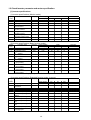
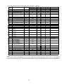
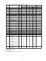
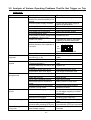
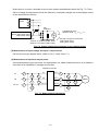
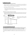
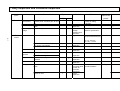
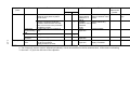
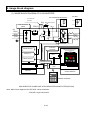
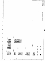
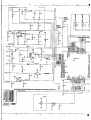
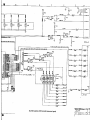
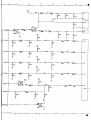
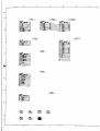
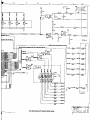
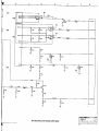
1
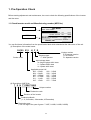
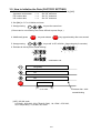
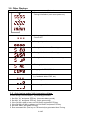
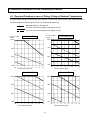
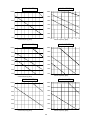
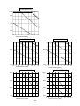
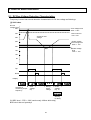
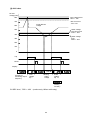
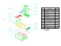
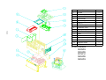
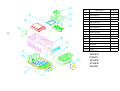
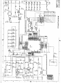
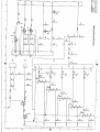
Looking for more information?
Visit us on the web at http://www.artisan-scientific.com for more information:
• Price Quotations • Drivers· Technical Specifications. Manuals and Documentation
Artisan Scientific is You~ Source for: Quality New and Certified-Used/Pre:-awned ECJuiflment
• Fast Shipping and DelIve1y
• Tens of Thousands of In-Stock Items
• Equipment Demos
• Hundreds of Manufacturers Supported
• Leasing / Monthly Rentals
Service Center Repairs
Experienced Engineers and Technicians on staff in our
State-of-the-art Full-Service In-House Service Center Facility
• Consignment
InstraView Remote Inspection
Remotely inspect equipment before purchasing with our
Innovative InstraView-website at http://www.instraview.com
We bUy used equipment! We also offer credit for Buy-Backs and Trade-Ins
Sell your excess. underutilized. and idle used equipment. Contact one of our Customer Service Representatives todayl
Talk to a live person: 88EM38-S0URCE fB88-887-68721 I Contact us by email: [email protected] I Visit our website: http://www.artisan-scientific.com
HITACHI INVERTER
SJ100 SERIES
SERVICE MANUAL
(ADJUSTMENT AND MAINTENANCE)
Model:
European Version
SJ100-002NFE to SJ100-022NFE
SJ100-004HFE to SJ100-075HFE
US Version
SJ100-002NFU to SJ100-022NFU
SJ100-004HFU to SJ100-075HFU
SJ100-037LFU
Japanese Version
SJ100-002LFR to SJ100-037LFR
SJ100-004HFR to SJ100-075HFR
After reading this manual, keep it at hand for future reference
Hitachi, Ltd.
Tokyo Japan
NBS585XA
INDEX
1-1
1. Pre-operation Check
1-1. Check inverter model and Manufacturing number
1-1
1-2. Check inverter parameter and motor specification
1-2
2. Measurement of The Internal Voltage Supply
2-1
3. Trouble Shoot
3-1
3-1. Error messages - Possible Cause and Remedy
3-1
3-2. Analysis of Various Operating Problems That Do Not Trigger an Trip Message
3-7
3-3. How to Initialize the Data (FACTORY SETTING)
3-8
3-4. Error Message Comparison
3-9
3-5. Other Displays
3-10
3-6. Auto tuning under high incoming voltage
3-10
4. Ambient Condition of the Frequency Inverter (Temperature, Altitude)
4-1
4-1. Required Derating in case of 50deg., 55 deg. of Ambient Temperature
4-1
4-2. Required derating toward altitude
4-4
5. Level of Each Detection
5-1
5-1. DC Bus Voltage Detection Characteristics
5-1
5.2. Output Current Detection Characteristics
5-3
5.3. Motor Temperature Detection (PTC)
5-4
5.4. Over Temperature Detection of the Frequency Inverter
5-4
6. Measurement & Replacement of Subassemblies
6-1
6-1. Insulation Measurement
6-1
6-2. Power Components Measurements
6-1
7. Maintenance and Inspection Procedure
7-1
7-1. Precautions
7-1
7-2. Measurement of Mains Voltage, Current and Power
7-1
7-3. Maintenance of Parts
7-4
7-4. If you install replacement INV at site
7-4
8. Daily Inspection and Periodical Inspection
8-1
9. Image block diagram
9-1
10. Spare parts list
10-1
10-1. parts list
10-1
10-2. I/O board compatibility
10-3. O, OI terminal adjustment procedure (C81, C82)
10-13
10-14
10-4. kW
10-15
setup procedure
10-5. I/O board schematic (circuit diagram)
- i -
10-16
Revisions
Revision history table
No.
Revision contents
Date of issue
-ⅰⅰ-
Manual No.
1. Pre-Operation Check
Before starting adjustment and maintenance, be sure to check the following specifications of the inverter
and the motor.
1.1 Check Inverter model and Manufacturing number (MFG No).
Inverter model
HITACHI
Model : SJ100-015NFE
HP/kW : 2 / 1.5
Input/Entree: 50,60Hz 200-240V
50,60Hz 200-240V
Output/Sortie: 1-360Hz 200-240V
MFG No. 78H T1129670060
MFG No.
1Ph
3Ph
3Ph
Hitachi, Ltd. MADE IN JAPAN
16.0 A
9.3 A
7.1 A
Date: 9708
NE16452-6
You can find these information from the specification label which attached at the side cover of the unit.
(1) Description of the model name.
SJ100 015
H F E
Structure type
F: With operator
Series name
Version number
E: European version
U: US version
R: Japanese version
Input voltage class
N: Single/3 phase 200V class
L: 3 phase 200V class
H: 3 phase 400V class
Applicable motor kW
002 : 0.2kW
022
004 : 0.4kW
030
005 : 0.55kW
037
040
007 : 0.75kW
011 : 1.1kW
055
015 : 1.5kW
075
: 2.2kW
: 3.0kW
: 3.7kW
: 4.0kW
: 5.5kW
: 7.5kW
(2) Description of MFG No.
7 8 H T112967 0060
Unique number
Production code
Revision of the inverter
Production Month
(1 - 9, 0:October, J:November, K:December)
Production year
(The unit digit of the year of grace. 7:1997, 8:1998, 9:1999, 0:2000)
1-1
1.2 Check Inverter parameter and motor specification.
[1] Inverter specifications.
(1) Inverter specifications (Monitor mode)
Display
order
1
2
3
4
5
6
7
8
9
Function name
Output frequency monitor
Output current monitor
Running direction monitor
Feedback data of PID
control monitor
Intelligent input terminal
condition monitor
Intelligent output terminal
condition monitor
Output frequency
converted value monitor
Trip monitor
Trip history monitor
Category
Monitor
Monitor
Monitor
Monitor
Screen display
Code display
d01
d02
d03
d04
EU
-
Initial
US
-
JPN
-
Remarks
Monitor
d05
-
-
-
Monitor
d06
-
-
-
Monitor
d07
-
-
-
Monitor
Monitor
d08
d09
-
-
-
Set
Set
Set
Screen display
Code display
F01
F02
F202
EU
0.0
10
10
Initial
US
0.0
10
10
JPN
0.0
10
10
Set
Set
F03
F203
10
10
10
10
10
10
Set
Set
F04
A--
00
00
00
Set
B--
Set
C--
Set
H--
(2) Inverter specifications (Basic function mode)
Display
Function name
Order
1
Output frequency setting
2
Acceleration time 1
Acceleration time 1
(2nd setting)
3
Deceleration time 1
Deceleration time 1
(2nd setting)
4
Running direction setting
5
Extended function
A group setting
6
Extended function
B group setting
7
Extended function
C group setting
8
Extended function
H group setting
Category
Remarks
Note; “-“ means hidden display ;depends on 2nd setting selection.
(3) Inverter specifications (Extended function mode : A group)
Displa
Function name
Category
y
Order
1
Frequency destination
Set
2
Running command
Set
destination
3
Base frequency
Set
nd
Base frequency(2 setting)
Set
4
Maximum frequency
Set
Set
Maximum frequency(2nd
setting)
5
External freq. setting start
Set
6
External freq. setting end
Set
7
External freq. setting start
Set
rate
8
External freq. setting end
Set
rate
9
External freq. start pattern
Set
10
Time constant of the filter
Set
of analog input
Screen display
Initial
Remarks
Code display
A01
A02
EU
01
01
US
01
01
JPN
00
02
A03
A203
A04
A204
50
50
50
50
60
60
60
60
60
60
60
60
A11
A12
A13
0
0
0
0
0
0
0
0
0
A14
100
100
100
A15
A16
01
8
01
8
01
8
1-2
(3) Inverter specifications (Extended function mode : A group)
Display
Function name
Order
11
Multi-speed 1 to 16
12
Jogging frequency
13
Stop mode of jogging
Category
Set
Set
Set
Screen display
Code display
A20 - A35
A38
A39
EU
0
1.0
00
Initial
US
0
1.0
00
JPN
Note 1
1.0
00
Remarks
Set
A41
A241
00
00
00
00
00
00
Set
A42
11
11
11
A242
11
11
11
A43
10.0
10.0
10.0
A243
10.0
10.0
10.0
Set
A44
A244
00
00
00
00
00
00
18
Torque boost mode
Torque boost mode(2nd
setting)
Level of manual torque
boost
Level of manual torque
boost (2nd setting)
Manual torque boost
frequency
Manual torque boost
frequency (2nd setting)
V/f characteristics
V/f characteristics(2nd
setting)
V-gain
Set
A45
100
100
100
19
20
21
22
23
Selection of DC braking
DC braking frequency
DC braking waiting time
DC braking force
DC braking time
Set
Set
Set
Set
Set
A51
A52
A53
A54
A55
00
0.5
0.0
0
0.0
00
0.5
0.0
0
0.0
00
0.5
0.0
0
0.0
24
25
26
27
Frequency upper limiter
Frequency lower limiter
Jump frequency 1-3
Jump frequency width 1-3
Set
Set
Set
Set
A61
A62
A63, A65, A67
A64, A66, A68
0.0
0.0
0.0
0.5
0.0
0.0
0.0
0.5
0.0
0.0
0.0
0.5
28
29
30
31
32
Set
Set
Set
Set
Set
A71
A72
A73
A74
A75
00
1.0
1.0
0.0
1.0
00
1.0
1.0
0.0
1.0
00
1.0
1.0
0.0
1.0
33
Selection of PID control
P gain
I gain
D gain
Scale conversion of
PID control
Feedback destination
Set
A76
00
00
00
34
35
Selection of AVR function
AVR voltage
Set
Set
A81
A82
02
230/400
02
230/460
02
200/400
36
-
Second acceleration time
Second acceleration
time(2nd setting)
Second deceleration time
Second deceleration
time(2nd setting)
Method to use 2nd
acceleration / deceleration
(Acc2 / Dec2)
Method to use 2nd
acceleration / deceleration
(Acc2 / Dec2)(2nd setting)
Acc1 to Acc2 changing
frequency
Acc1 to Acc2 changing
frequency(2nd setting)
Dec1 to Dec2 changing
frequency
Dec1 to Dec2 changing
frequency(2nd setting)
Acceleration characteristic
Deceleration characteristic
Set
A92
A292
15.0
15.0
15.0
15.0
15.0
15.0
Set
A93
A293
15.0
15.0
15.0
15.0
15.0
15.0
Set
A94
00
00
00
A294
00
00
00
A95
0.0
0.0
0.0
A295
0.0
0.0
0.0
A96
0.0
0.0
0.0
A296
0.0
0.0
0.0
A97
A98
00
00
00
00
00
00
14
15
16
17
-
37
38
-
39
40
41
42
Set
Set
Set
Set
Set
Note 1; A20;0, A21;5, A22;10, A23;15,A24;20, A25;30, A26;40, A27;50, A28; 60,A29--A35;0
1-3
(4) Inverter specifications (Extended function mode : B group)
Display
Function name
Order
1
Selection of restart mode
2
Allowable UV time
3
Retry waiting time
Category
Set
Set
Set
Screen display
Code display
B01
B02
B03
EU
00
1.0
1.0
Initial
US
00
1.0
1.0
JPN
00
1.0
1.0
Remarks
4
Electronic thermal level
Set
B12
note
note
note
-
Electronic thermal level
(2nd setting)
Electronic thermal
characteristics
Electronic thermal
characteristics (2nd setting)
Overload restriction
operation mode
Overload restriction level
Set
B212
note
note
note
Set
B13
01
01
00
Set
B213
01
01
00
Set
B21
01
01
01
Set
B22
note
note
note
Set
B23
1.0
1.0
1.0
Set
B31
01
01
01
Set
Set
Set
Set
B81
B82
B83
B84
80
0.5
5
00
80
0.5
5
00
80
0.5
12
00
Set
Set
B85
B86
01
1.0
02
1.0
00
1.0
Set
Set
B87
B88
00
00
00
00
00
00
Set
B89
01
01
01
Set
B90
00
00
00
Set
Set
B91
B92
00
00
00
00
00
00
5
6
7
8
9
10
11
12
13
14
15
16
17
18
19
20
21
Deceleration rate while
overload restriction
Selection of software lock
Analog meter adjustment
Start frequency adjustment
Carrier frequency
Data initialization or
Trip history clear
Initialization mode
Frequency converting
value
STOP key condition
Restart mode after FRS
invalid
Monitor contents
for OPE-J
Dynamic braking usage
ratio
Stopping mode selection
Cooling fan control
selection
1-4
Rated current of
each inverter
Rated current of
each inverter
Rated current
* 1.25 for each
inverter
(5) Inverter specifications (Extended function mode : C group)
Display
Order
1
2
3
4
5
6
Input terminal 1 assign
Input terminal 2 assign
Input terminal 3 assign
Input terminal 4 assign
Input terminal 5 assign
Input terminal 6 assign
Set
Set
Set
Set
Set
Set
Screen display
Code display
C01
C02
C03
C04
C05
C06
7
8
9
10
11
12
Input terminal 1 condition
Input terminal 2 condition
Input terminal 3 condition
Input terminal 4 condition
Input terminal 5 condition
Input terminal 6 condition
Set
Set
Set
Set
Set
Set
C11
C12
C13
C14
C15
C16
00
00
00
00
00
00
00
00
00
01
00
00
00
00
00
00
00
00
13
14
15
16
Output terminal 11 assign
Output terminal 12 assign
FM terminal condition
Function of AL terminal
setting
Output terminal 11
condition
Output terminal 12
condition
AL output terminal
condition
Level of overload signal
Set
Set
set
Set
C21
C22
C23
C24
01
00
00
05
01
00
00
05
01
00
00
05
Set
C31
00
00
00
Set
C32
00
00
00
Set
C33
01
01
01
Set
C41
note
note
note
Set
C42
0.0
0.0
0.0
Set
C43
0.0
0.0
0.0
Set
C44
3.0
3.0
3.0
Set
Set
Set
Set
Set
Set
Set
C81
C82
C91
C92
C93
C94
C95
--00
0000
-D0001
--
--00
0000
-D000
--
--00
0000
-D000
--
17
18
19
20
21
22
23
24
25
26
27
28
29
30
Function name
Arrival frequency
while acceleration
Arrival frequency
while deceleration
Level of deviation signal
under PID control
Analog input O adjustment
Analog input OI adjustment
Debug mode selection
Core monitor address
Core monitor data
Core set address
Core set data
Category
Note 1
USP function
EU
00
01
02
03
18
09
Initial
US
00
01
16
13
09
18
JPN
00
01
02
03
09
18
Remarks
Note 1
Rated current of
each inverter
(NC) is allocated on US version and even another function such as CF1 is set, NO/NC
parameter is still the same. Therefore, please make sure the NO/NC parameter to suit the application.
1-5
(6) Inverter specifications (Extended function mode : H group)
Display
Order
1
2
3
-
4
5
6
7
8
11
12
13
14
15
16
17
-
Function name
Auto tuning setting
Motor data selection
Motor data selection(2nd
setting)
Motor capacity setting
Motor capacity setting(2nd
setting)
Motor poles setting
Motor poles setting(2nd setting)
Speed response setting
Speed response setting(2nd
setting)
Motor stabilization constant
setting
Motor stabilization constant
setting(2nd setting)
Motor constant R1 setting
Motor constant R1 setting(2nd
setting)
Motor constant R2 setting
Motor constant R2 setting(2nd
setting)
Motor constant L setting
Motor constant L setting(2nd
setting)
Motor constant Io setting
Motor constant Io setting(2nd
setting)
Motor constant J setting
Motor constant J setting(2nd
setting)
Motor constant R1(auto tuning
data)
Motor constant R1(auto tuning
data,2nd setting
Motor constant R2(auto tuning
data)
Motor constant R2(auto tuning
data,2nd setting
Motor constant L(auto tuning
data)
Motor constant L(auto tuning
data,2nd setting
Motor constant Io(auto tuning
data)
Motor constant Io(auto tuning
data,2nd setting
Motor constant J(auto tuning
data)
Motor constant J(auto tuning
data,2nd setting
Catego Screen display
ry
Code display
Set
H01
Set
H02
Set
H202
Initial
Remarks
EU
00
00
00
US
00
00
00
JPN
00
00
00
Set
Set
H03
H203
*3
*3
*3
*3
*3
*3
Set
Set
H04
H204
H05
H205
4
4
20
20
4
4
20
20
4
4
20
20
Set
H06
100
100
100
Set
H206
100
100
100
Set
set
H20
H220
*2
*2
*2
*2
*2
*2
Set
Set
H21
H221
*2
*2
*2
*2
*2
*2
Set
H22
H220
*2
*2
*2
*2
*2
*2
H23
H223
*2
*2
*2
*2
*2
*2
Set
H24
H224
*2
*2
*2
*2
*2
*2
*1
H30
*2
*2
*2
*1
H230
*2
*2
*2
*1
H31
*2
*2
*2
*1
H231
*2
*2
*2
*1
H32
*2
*2
*2
*1
H232
*2
*2
*2
*1
H33
*2
*2
*2
*1
H233
*2
*2
*2
*1
H34
*2
*2
*2
*1
H234
*2
*2
*2
*1; don’t change the data
*2 ; factory set
*3 ; specified by the capacity of each inverter
1-6
[2] Motor specifications.
Output voltage
V
Output
frequency
0
Hz
Hz
Motor MFG number
Motor output
kW
Rated current
Amps
Motor poles
p
Rated voltage
V
Motor rated rpm
rpm
Rated frequency
Hz
Starting current
Amps
Acceleration time
sec
sec
[3] Load conditions
Equipment name
Torque characteristics
Required torque
Nm
Deceleration time
Load inertia (J)
kgm2
Variable speed range
Hz
1-7/E
to
Hz
2. Measurement of the Internal Voltage Supply
There are PV5L, PV24L and NV12L internal DC voltage supplies. These supplies are isolated from the
main high voltage portion. And it is not possible to measure DC voltages at the non isolated portion.
Please make measurements for above mentioned voltages for the isolated portion.
Check pad of NV12
Check pad of PV24
Check pad of PV5
1 pin of TM2 is “L”common
PV5L supply voltage
Supplies 5V for I/O board.
Nominal voltage : min. 4.90Vdc to max. 5.20Vdc
Check PV5(address 1C) <- L
PV24L supply voltage
Supplies 24V to interface voltage supply, which is supplied to input terminals.
Nominal voltage : min. 21.60Vdc to max. 26.40Vdc
Check PV24(address 1A) <- L
NV12L supply voltage
Supplies -12Vdc to remote operator (DOP/DRW’s yellow back light ).
Nominal voltage : max. -10.80Vdc to min. -17.5Vdc
Check NV12(address 3A) <- L
“H” terminal voltage
Suppiles 10V to “H” terminal
Nominal voltage : min 9.5Vdc to max 11.5Vdc
Check “H” <-> “L” with VR (1kohm)
“Potentiometer function on the front case
Set “A01” :”00”
Monitor “F01” display 0 <-> 50(60) with clockwise and anti clockwise.
Cooling FAN voltage (PV24N)
Supplies 24V to cooling FAN .
Nominal voltage min 19.9Vdc to max 27.2Vdc.
Check Red wire <- Black wire with the FAN.
Check the FAN working, direction(from down to up).
2-1/E
3. Trouble Shoot
3-1. Error Messages - Possible Cause and Remedy:
(1) Over current 1 (E 01, E 02, E 03, E 04)
Phenomena:
Over current (CT or Rsh;gate driver IC) for each condition.
E 01 :
Over current during constant speed operation.
E 02 :
Over current during deceleration.
E 03 :
Over current during acceleration.
E 04 :
Over current at other condition than above mentioned.
(such as injection brake)
Cause:
Remedy:
Load changed rapidly.
Eliminate rapid changed in load.
Cause:
Remedy:
Sort circuit or earth contact (ground fault) in the motor or the motor cable.
Check with Megger. If the motor cable is disconnected from the inverter, the over
current should not be detected anymore.
Cause:
Remedy:
A single-phase power failure (fuse, wire, ...) can cause a shutdown in certain
under load situations..
Check all these mains phases and the mains fuses, preferably by comparison of
the three (two in case of single phase inverter) mains currents in a steady
operating state.
Cause:
Remedy:
The motor is switched with a motor contactor during frequency inverter operation.
Switching over the motor is inhibited.
Cause:
Remedy:
Defect in the power component.
Check the IGBT portion of ISPM.
Cause:
Remedy:
Rapid acceleration or deceleration.
Set suitable acceleration or deceleration time.
Cause:
Remedy:
Starting frequency is too high.
Set starting frequency as low as possible.
Way to Reset:
A
SJ100 has two kinds of detection; CT and Rsh. To resolve the detection at site, check the following
procedure.
1. Connect DOP/DRW.
2. Set F38 INIT DEBG ON. (to access debug mode)
3. Set F22 IPS POWR ALM mode, don’t set retry mode.
4. Test run and wait Over Current trip.
5. Set Core address “FBE4” if it’s 4kW or less.
5. Set Core address “FBE2” if it’s 5.5kW or above.
3-1
Specimen ;
“CO FBE4 01 0000” ; under normal; 0Hz
“CO FBE4 15 0203” ; under over.C trip
“CO FBE4 15 C203” ; under OC.Drive trip.
“CO FBE4 15 4103” ; under OC.Accel trip
“FBE4” or “FBE2” is 1 byte data, the data is hex data. Example “4103”; “03” has no meaning.
Resolve “41”h bit by bit,
“41”h -> “0100 0001”b
if you found “xxxx xxx1” ; this means Over current detection from CT (CTU or CTW)
if you found “xxxx xx1x” ; this means Over current detection from Rsh
Standard operator is not available on this trouble shooting.
(2) Overload (E 05)
Phenomena:
Overload (detected by CT) of the inverter.
This error can be reset 10 seconds after the E05 came out.
Cause:
Remedy:
Motor load is heavy.
Reduce the load and/or increase thermal level and/or use bigger capacity of
frequency inverter.
Cause:
Remedy:
V-Boost value is high.
Reduce V-Boost value or increase thermal level and/or use bigger capacity of
frequency inverter.
Cause:
Set wrong value for electronic thermal level [b12] and/or electronic thermal
characteristic [b13].
Set suitable value.
Remedy:
Cause:
Remedy:
Set wrong value for the reactive current of the motor.
Set suitable value. Reactive current value which should be input by function mode
is a value measured at 50Hz (60Hz) without load.
Way to Reset:
A
(3) Braking Resistor Overload (over voltage) (E 06)
Phenomena:
Over Voltage detection after BRD%ED was run out.
Cause:
Remedy:
BRD selection is not suitable.
Check BRD %ED, BRD resistor ohm, BRD resistor Wattage, BRD resistor wire,
machine inertial, operation cycle.
Way to Reset:
A
3-2
(4) Over voltage (E 07)
Phenomena:
Over voltage at DC bus line of the frequency inverter.
Cause:
Mains voltage too high, mains voltage fluctuation or rapid mains voltage return
(choke energy leads to voltage increase).
Make sure that mains voltage is within tolerance limits.
Remedy:
Cause:
Remedy:
Cause:
Remedy:
In case SJ100 is used in combination with a regenerative braking unit(ISPM)/
resistor but the regenerative braking unit(ISPM)/resistor does not function.
Replace regenerative braking unit(ISPM)/resistor.
In case SJU100 is used in combination with a raking resistor but the braking
resistor cannot absorb the regenerative energy.
Re-calculate and use suitable braking resistor.
Cause:
Remedy:
Deceleration time is too short.
Make deceleration time longer, use braking unit (resistor), use bigger capacity of
frequency inverter.
Way to Reset:
A
(5) Under voltage (E 09)
Phenomena:
Under voltage at DC bus line of the frequency inverter.
Cause:
Remedy:
The mains voltage is not available or not within the tolerance limits.
Check all 3 (or 2) mains power supply voltage that it is within its specification.
Cause:
Thyristor for smooth charging is defect and DC bus voltage drops while operation
due to current flows through smooth charging resistor.
Change ISPM.
Period of instantaneous power failure is longer than the set value [b02], or DC bus
voltage go down to its detecting level while instantaneous power failure.
Get rid of the instantaneous power failure, evaluate the power supply system, set
bigger value for [b02].
Remedy:
Cause:
Remedy:
Cause:
Remedy:
One of the AC voltage is missing (applied only for 3 phase INV)
Check AC line voltage , check the fuses.
Way to Reset:
A
(6) EEPROM error (E 08)
Phenomena:
Abnormal situation occurs at the memory portion of the frequency inverter due to
incoming noise etc..
Cause:
Remedy:
Influenced by Electrical Magnetic Interference.
Keep such noise source away from the frequency inverter.
Cause:
Remedy:
Ambient temperature is too high.
Take countermeasure against high ambient temperature.
3-3
Cause:
Remedy:
Re-power up the frequency inverter short time after power off. It is necessary to
keep several seconds after power off to memorize the current data at EEPROM. If
this time is too short, this storage performance cannot be done and leads to
EEPROM error.
Keep certain time between power off and re-power up.
Cause:
Remedy:
You didn’t wait 6 seconds or more at FACTORY SETTING.
Please try FACTORY SETTING again.
Cause:
RS terminal was keeping “ON” at power off. (If RS is on, INV can not write the
correct data to EPROM at power off, next power on E08 will come out.)
Please don’t use “RS” terminal “ON” at power off.
Remedy:
Cause:
EEPROM is defect.
Remedy:
Change unit.
After you reset the INV, please make sure the parameters especially maximum freq. / Acc /Dec
time / Low limit freq. to prevent any damage.
Way to Reset:
A or Power off
(7) CT error (E 10)
Phenomena:
When abnormality noise is near the INV or an abnormality (offset level is out of
spec.) occurs on built in CT.
Cause:
Remedy:
Influenced by Electrical Magnetic Interference. (such as near contactor on/off)
To Resolve if it’s influence, use another power line and don’t connect motor wires,
control wires. If no error comes out, resolve noise causes.
Cause:
Remedy:
CT offset level failure
To Resolve if it’s failure, use another power line and power on and check if E10
comes out at power on. If E10 came out , use (replace) another INV(ISPM).
Way to Reset:
A or Power off
(8) CPU error (E 11, E 22)
Phenomena:
Abnormal situation or malfunction of micro processor inside frequency inverter.
E 11 :
CPU error from MCU inside core.
E 22 :
CPU error from MCU on I/O board.
E22 is produced by MCU on I/O board and the causes is communication error between ISPM & MCU
on I/O board.
Cause:
Remedy:
Cable (between ISPM and I/O board)was cut. (E22)
Replace the cable.
Cause:
Remedy:
Dusts on the pins of CN2 on I/O board. (E22)
Remove the dusts.
Cause:
Remedy:
Influenced by Electrical Magnetic Interference.
Keep such noise source away from the frequency inverter.
Cause:
Remedy:
Ambient temperature is too high.
Take countermeasure against high ambient temperature.
3-4
Cause:
Remedy:
Component itself is defect.
Replace ISPM (in case of E 11) or I/O board board (in case of E 12).
(9) External Trip (E 12)
Phenomena:
Trip due to have inputted an external signal to “EXT” input terminal of the
frequency inverter.
Cause:
Remedy:
Faulty external device or equipment gives frequency inverter a trip requirement
when external trip function (EXT) is selected.
Evaluate external device or equipment which is connected to frequency inverter.
Way to Reset:
A
(10) USP error (E 13)
Phenomena:
Unexpected Start Protection. This error can occur when “USP” function is
selected.
Cause:
Remedy:
Frequency inverter trips when it is powered up with RUN command is given.
Disable RUN command when power up the frequency inverter. Or disable USP
function if possible to the system.
Way to Reset:
A
or set RUN command off (stop)
(11) Ground fault error (E 14)
Phenomena:
Earth contact in the motor or the motor cable or in the IGBT. Frequency inverter
detects this earth contact only at power up.
To resolve the causes , please power off and disconnect the motor wire at INV (UVW)terminal.
Cause:
Remedy:
Earth contact in the motor or the motor cable.
Check the impedance between output portion(wire and motor) and earth.
Cause:
Detection circuit/IGBT of the inverter is defect. If the motor and the motor cable is
disconnected from the frequency inverter, the ground fault should not be detected
anymore.
Please disconnect the motor and the motor cable.
If E14 comes out at power on, please replace the unit.
Remedy:
Way to Reset:
Don’t reset.
(12) Over voltage at source (E 15)
Phenomena:
High voltage at power source line. Frequency inverter cannot protect source over
voltage. If it is too high, frequency inverter will be damaged.
Cause:
Remedy:
Source voltage is too high.
Check the source voltage continously.
Insert AC reactor at source lines.
Way to Reset:
A
3-5
(13) Over temperature (E 21)
Phenomena:
Temperature sensor which located close to IGBT inside ISPM shows a too high
temperature.
Cause:
Remedy:
Ventilator blocked. (for models which has ventilator.)
Check ventilator
Cause:
Remedy:
The frequency inverter does not get enough cooling air.
Check cabinet ventilation, air filters, and ventilation openings in the cabinet.
Way to Reset:
A
(14) PTC error (E 35)
Phenomena:
Resistance of motor thermistor is high. This error can occur when you select
“PTC” function.
Cause:
Remedy:
Too much load of the motor.
Reduce the load, use bigger motor.
Cause:
Remedy:
Motor thermistor is not connected while PTC function is selected.
Disable PTC function when it is not used.
Cause:
Characteristics of the motor thermistor is not suitable. Frequency inverter gives
PTC error when the resistance value becomes more than 3k ohm +-10%.
Use motor which has suitable thermistor for the inverter.
Or change thermistor characteristics of the thermistor by debug mode.
Remedy:
Way to Reset:
A
Explanation of the way to reset.
A : Make close the terminals between RS and P24 (CM1 only for Japanese version) on the I/O board, or
press “STOP/RESET” key of the operator.
3-6
3-2. Analysis of Various Operating Problems That Do Not Trigger an Trip
message.
Problem
The motor does not start
Possible cause
Remedy
Mode of frequency command [A01] Check each mode again
and/or Run command [A02] is not
proper
Incorrect power supply condition
Check that the power supply is
within its specification
Inverter is in trip mode
Get rid of the trip cause
0 Hz of Multi-stage speed is given
FRS and/or RS is remaining
Make FRS and RS invalid
0 Hz command is given
Each phase to phase voltage does Replace the unit
not balance. (out of +-3%)
Load is too heavy
Decrease the load or use bigger
capacity of inverter and motor
Set as follows
If you use DOP or DRW, DIP
switch selection of the operator is
1 2 3 4
incorrect.
ON
OFF
Rotation direction is
opposite
Motor does not increase
speed
The inverter cannot be
programmed
Unstable rotation of the
motor
Inverter Failure
Wiring of the motor cable is
incorrect (U, V, W)
Setting of [F04] is incorrect
Motor load is too heavy
(Overload limitation)
External frequency set (VR) is out
of order
Frequency limiter [A61] is set
Acceleration time is too short
Software lock is selected [b31]
While INV running
RS or FRS command is given
Multi stage speed command is
given
Loose connection of DOP/DRW
Inverter is in trip mode
Motor load is changing heavily
Data is not changed
Source voltage is changing
Mechanical resonance
Forgot to press [STR] key
Cannot change data by
Copy Unit
Turn main power off within 6
seconds after pressing [STR] key
Turn power off within 6 seconds
after started copying
3-7
Same as J300, J100,L100
Replace the unit
Check the wiring of the motor
cable
Check the setting
Remove or decrease the motor
load
replace VR
Eliminate frequency limiter
Set longer acceleration time
Make software lock invalid
Stop the INV
Make them invalid
Make inverter in stop mode
Connect DOP/DRW properly
Reset the inverter
Reduce the motor load changing
or use bigger capacity of inverter
and motor
Reduce the changing
Change output frequency
Press [STR] key after changing
data
Make sure to wait at least 6
seconds after [STR] key is pressed
Make sure to wait at least 6
seconds
3-3. How to Initialize the Data (FACTORY SETTING)
1. Select the mode of initialization data to which you want to initialize by [b85].
Japanese version data
----->
Set “00” and store
EU version data
----->
Set “01” and store
US version data
----->
Set “02” and store
2. Set [b84] to “01” to initialize and store.
3. Keep pressing
FUNC.
1
2
keys at the same time.
(If front case is not closed by the screw, difficult to press 3keys.)
4. Additionally press
5. Keep pressing
STOP
RESET
FUNC.
1
key and release
2
STOP
RESET
key approximately after one second.
keys until “d 00” will blink. (Approximately 2 seconds.)
6. Release all the keys after starts blinking.
Initialization end
FUNC.
ON (press)
1
ON
2
ON
STOP
RESET
ON
1s or more
Release after “d 00”
started blinking
[c95] ; INV kW code
01;0.2kW , 02;0.4kW , 03;0.75kW (0.5 kW) , 04;1.5kW , 05;2.2kW ,
06;3.7kW(4.0kW) , 07;5.5kW, 08;7.5kW
3-8
3-4. Error Message comparison
Digital Panel
DOP / DRW
OC.
OC.
OC.
Drive
Over current while deceleration (CT or
gate driver IC)
Decel
Over current while acceleration (CT or
gate driver IC)
Accel
Over.
C
Over.
L
OL.
Contents
Over current while constant speed
driving (CT or gate driver IC)
Over current at other condition than
above(such as 0Hz,injection brake)
(CT or gate driver IC)
Over load
(Possible to reset after 10 seconds
has passed, detected by CT)
Over voltage after the BRD%ED
was run out. (DC bus)
BRD
Over.
Over voltage (DC bus)
V
EEPROM error
(Check the parameters again if this
error occurred)
Under voltage (DC bus)
EEPROM
Under.
V
CT offset error such as external noise
or CT itself
CT
CPU error
CPU 1
CPU 2
External error
External
USP error
USP
GND
OV.
OH
Ground fault at power-on detected by
CT
Flt
Over voltage at source (DC bus)
(continuously 100sec while stop)
SRC
Over temperature (in the ISPM)
FIN
PTC error (only terminal 5 )
PTC
3-9
3-5. Other Displays
Digital Panel
Contents
- Reset terminal is ON
- During initialization (such as at power-on)
- Voltage is within UV level
- Power OFF
- During retry mode
- During initialization as EU settings
- During initialization as US settings
- During initialization as Japanese settings
- Erasing trip histories
- Copying with DRW,DRW-2
- When there is no data
(i.g. feedback data of PID, etc.)
Auto tuning was done.
Auto tuning was failed.
3-6. Auto tuning under high incoming voltage
If Auto tuning is not successful , try following procedure.
1. Set C91 “01” and press STR key. (to access debug mode)
2. Set H01 “01” and press STR key. (to do auto tuning)
3. If the SJ100 is 4kW or less, set C94 “fb82” and press STR key.
3. If the SJ100 is 5.5kW or above, set C94 “fb80” and press STR key.
4. Set C95 “0000” and press STR key.
5. Run command ON. (Run key or FW terminal) to get started Auto Tuning.
3-10/E
4. Ambient Condition of the Frequency Inverter
4-1. Required Derating in case of 50deg, 55deg of Ambient Temperature
Inverter ratings can be influenced by many factors. You can find in this section, the relation between
ambient temperature and output current (%) and carrier frequency.
Standard ratings in 40 degree C
Top cover removed condition in 50 degree C max.
Top cover removed condition in 55 degree C max.
% rate of output
current
% rate of output
current
SJ100-002NFE(U)
100%
100%
90%
90%
80%
80%
70%
70%
0.5 2
4
6
8
10
Carrier frequency [kHz]
12
14
SJ100-004NFE(U)
0.5 2
4
6
8
10
Carrier frequency [kHz]
16
12
14
16
14
16
SJ100-015NFE(U)
SJ100-007NFE(U)
100%
100%
90%
90%
80%
80%
70%
70%
0.5 2
4
6
8
10
Carrier frequency [kHz]
12
14
16
4-1
0.5 2
4
6
8
10
Carrier frequency [kHz]
12
SJ100-037LF(U)
SJ100-022NFE(U)
100%
100%
90%
80%
90%
70%
60%
80%
50%
70%
0.5 2
4
6
8
10
Carrier frequency [kHz]
12
14
40%
16
100%
100%
90%
90%
80%
80%
70%
70%
60%
60%
50%
50%
0.5 2
4
6
8
10
Carrier frequency [kHz]
12
14
40%
16
100%
100%
90%
90%
80%
80%
70%
70%
60%
60%
50%
50%
0.5 2
4
6
8
10
Carrier frequency [kHz]
12
14
16
0.5 2
4
6
8
10
Carrier frequency [kHz]
12
14
16
14
16
SJ100-022HFE(U)
SJ100-015HFE(U)
40%
12
SJ100-007HFE(U)
SJ100-004HFE(U)
40%
0.5 2
4
6
8
10
Carrier frequency [kHz]
14
40%
16
4-2
0.5 2
4
6
8
10
Carrier frequency [kHz]
12
SJ100-040HFE(U)
100%
90%
80%
70%
60%
50%
40%
0.5 2
4
6
8
10
Carrier frequency [kHz]
12
14
16
SJ100-055LFU
SJ100-075LFU
100%
100%
90%
90%
80%
80%
70%
0.5 2
4
6
8
10
Carrier frequency [kHz]
12
14
16
70%
0.5 2
4
6
8
10
Carrier frequency [kHz]
SJ100-055HFE(U)
12
14
16
14
16
SJ100-075HFE(U)
100%
100%
90%
90%
80%
80%
70%
70%
0.5 2
4
6
8
10
Carrier frequency [kHz]
12
14
4-3
16
0.5 2
4
6
8
10
Carrier frequency [kHz]
12
4-2. Required derating toward altitude
100%
90%
80%
70%
2000
1000
3000
4000
Altitude [m]
Example of calculation
SJ100-007NFE (4 Amps) is installed at 2000m of altitude and 16kHz of carrier frequency.
Required derating of output frequency of this case will be as follows.
4 [Amps] * 90% * 95% = 3.4 [Amps]
Carrier frequency derating
Altitude frequency derating
<Note 1> When the top cover is removed for the high ambient temperature, inverter should be installed
in an enclosure of IP 4* (see EN60529) to comply with LVD directive.
<Note 2> If class B of EMC directive is required, carrier frequency must be set to 5kHz.
4-4/E
5. Level of Each Detection
5-1. DC Bus Voltage Detection Characteristics
Frequency inverter has several detection characteristics for DC bus voltage as followings.
[1] 200V class
DC bus
voltage [Vdc]
400
Over voltage level
395V +- 20V
350
BRD on/off level
370V +-20V
Actual DC bus
voltage
300
Under voltage
recovering level
220V +- 10V
250
200
Under voltage
level
190V +- 10V
150
100
50
0
Trip
Trip
Trip
Reset
on
on
Display
example of
monitoring output
frequency
Over
voltage
trip
During
Under
voltage
Under
voltage
trip or
Waiting
for Retry
OV.SRC level ; 375V +- 20V (continuously 100sec while stop)
BRD circuit has no hysterisys
5-1
[2] 400V class
DC bus
voltage [Vdc]
800
Over voltage level
790V +- 40V
700
BRD on/off level
740V+-40V
Actual DC bus
voltage
600
Under voltage
recovering level
440V +- 20V
500
400
Under voltage
level
380V +- 20V
300
200
100
0
Trip
Trip
Reset
Trip
on
on
Display
example of
monitoring output
frequency
Over
voltage
trip
During
Under
voltage
Under
voltage
trip or
Waiting
for Retry
OV.SRC level ; 750V +- 40V (continuously 100sec while stop)
5-2
5-2. Output Current Detection Characteristics
Frequency inverter has several detection characteristics for output current to protect IGBT from break
down, or to protect motor from over heat.
[1] Over current
Frequency inverter shuts off the output instantaneously when output current exceeds to 220%(190)
of its rated current. (OC level is no link with Electronic thermal level)
e.g. Over current protection level of SJ100-015NFE (7.1 Amps of rated current) is
7.1 [Arms] * 200% = 14.2 [Arms] = 20.1 [A peak]
[2] Over load (Electronic thermal protection)
Frequency inverter shuts off the output when integration value of output current and time exceeds
specific value.
time
E-Thermal Level = [100]
180s
No over load trip with
115% load
Over Current trip
220%(-> 4kW)
120s
190%(5.5kW ->)
150%, 60s
60s
180%, 10s
0
100%
150%
220%(190%)
% output current of the rated current of the frequency inverter
This Electronic thermal level can be changed from 50% to 120%. (Initial setting is 100%.)
time
180s
E-Thermal Level = [50]
120s
150%, 60s
60s
180%, 10s
0
50%
150%
100%
% output current of the rated current of the frequency inverter
5-3
220%(190%)
5-3. Motor Temperature Detection (PTC)
Frequency inverter has a motor temperature sensor input (PTC input : PTC resistor).
When the resistance value is more than 3k ohm +-10%, the frequency inverter trips with “E35”.
SJ100 inverter
U
V
W
L 5(PTC)
Motor
PTC thermistor
Except Japanese version
5-4. Over Temperature Detection of the Frequency Inverter
Frequency inverter has a temperature detection against power devices of the main circuit. Frequency
inverter shuts down the output when temperature around IGBT comes up to 120 degree C.
5-4/E
6. Measurement & Replacement of Subassemblies
6-1. Insulation Measurement
For SJ100 inverter, do not perform insulation measurements , otherwise MOV will be damaged.
(MOV; between R(L1)-G, S(L2)-G, T(L3)-G)
6.2. Power Components Measurements.
When checking the power components, the following procedure is recommended:
!
Clear voltage
!
Wait for capacitors discharge
!
Check capacitors for neutrality
!
Disconnect mains and motor wires
!
Test the diodes and IGBTs using a universal tester with a diode function.
Visual check is important for the ISPM, check the appearance such as smoke trace.
Note: In this test, the absolute values are not so important, since they depend strongly on the test
device used. The uniformity of the measured value is more important.
[1] DC BUS Measurement
Check “+” <- “ - ” voltage Zero.
Resistance Measurement
From
To
+
-
Allowable Value
50kohm or more
P1, PD are located on the CB board / snubber board.
Check “+1” and “+” terminal are shorten by (copper) bar.
[2] Soft charge Resistor (RS) , Thyristor (THY) Measurement
Resistance Measurement
Allowable Value
From
To
P1
PD
15 to 25 ohm
PD
P1
(From P1 To PD
From PD To P1 ;if RS was opened)
6-1
[3] Rectifier Measurement
+1
RB
+
RS
P1 THY PD
CTU
R(Ll)
U
V
W
+
S(L2)
T(L3)
CTW
Rsh
Main circuit of SJ100
This is to measure 6 rectifiers of the input side.
Resistance Measurement
Allowable Value
From
To
R(Ll)
S(L2)
50kohm or more
S(L2)
R(Ll)
S(L2)
T(L3)
T(L3)
S(L2)
T(L3)
R(Ll)
R(Ll)
T(L3)
R(Ll)
R(Ll)
S(L2)
S(L2)
T(L3)
T(L3)
Each R(Ll), S(L2) and
50kohm or more
T(L3)
Each R(Ll), S(L2) and
50 ohm or less
T(L3)
Each R(Ll), S(L2) and
P1
50 ohm or less
T(L3)
P1
Each R(Ll), S(L2) and 50kohm or more
T(L3)
To make sure MOV, visual check of MOV is necessary on the ISPM.
P1
R(L1)
S(L2)
T(L3)
If the result is out of its spec, replace the unit. ( relative check is important )
MOV(ZNR);ZNR1,ZNR2,ZNR3 are for phase to phase
MOV(ZNR);ZNR4,ZNR5,ZNR6 are for phase to ground
6-2
[4] IGBT Measurement
Resistance Measurement
From
To
+
U
+
V
+
W
U
+
V
+
W
+
U
V
W
U
V
W
-
Allowable Value
+
50kohm or more
U
V
W
50 ohm or less
Rsh
50 ohm or less
50kohm or more
DC current detecting
resistor (shunt resistor)
(Order of mili ohm)
If the result is out of its spec, replace the unit.
Please note that this cannot cover 100% to find IGBT failure because if the power devices in failure,
sometimes you can find the failure in components while they are activated. (You cannot find the failure
while they are not activated.)
[5] Cooling FAN voltage circuit in the ISPM (PV 24N)
Check “b92” is preset “”00 (FAN to be worked) and disconnect the cooling FAN
Resistance Measurement
From
To
Pin(up) (Red)
Pin(down) (Black)
Pin(up) (Black)
Pin(down) (Red)
( relative check is important )
Allowable Value
20kohm or more
50ohm or less
[6] Cooling FAN
Disconnect the cooling FAN and measure impedance of FAN circuit.
Resistance Measurement
From
To
Red wire
Black wire
Black wire
Red wire
( relative check is important )
Allowable Value
50kohm or less
100kohm or more
[7] BRD(RB,+,-)
Disconnect BRD resistor.
Red wire, Black wire mean tester’s wires.
Resistance Measurement
Allowable Value
Allowable Value
+
RB
Diode drop V
100kohm - 400kohm
0.3 – 0.5
Black wire
Red wire
8ohm – 14ohm
OL
Red wire
Black wire
(only reference)
Resistance Measurement
Allowable Value
Allowable Value
RB
Diode drop V
100kohm – 700kohm
OL(initial charge)
Black wire
Red wire
2kohm – 4kohm
OL
Red wire
Black wire
(only reference)
6-3/E
7. Maintenance and Inspection Procedure
7-1. Precautions
(1) Maintenance and Inspection Precautions
Be sure to check the followings before starting maintenance and inspection because there is a
danger of electrical shock.
!
Display on the digital operation panel and POWER indication has been turned OFF.
!
The voltage between + and - is 15Vdc or lower.
!
Discharging resistor (500 ohm 30W for 200V class, 1k ohm 60W for 400V class) has been
connected between + and - terminals for 15 seconds or more after main power had turned off,
(2) General Precautions
!
Always keep the unit clean so that no dust nor other foreign materials come inside of the
frequency inverter.
!
Pay attention to broken lines and faulty connections. Firmly connect terminals and connectors.
!
Keep frequency inverter away from moisture and oil.
!
Dusts, steel filings, swarf , and other foreign materials can damage insulation and causing
unexpected accidents/failure. Please pay attention to them.
7-2. Measurement of Mains Voltage, Current and Power
General measuring instruments for mains voltage, current and power are shown in Table 7-1.
The voltage to be measured is the effective value of fundamental wave, and the power to be measured
is the total effective value.
(1) Measurement of output voltage
Moving iron type instrument does not show accurate values for measurement of the output voltage.
Make measurements according to the method shown in Fig. 7-3 (table 7-1) or using the circuit
indicated in Fig. 7-1 and 7-2.
Frequency
Inverter
Motor
U
Load
V
W
2W
220kohm
Fundamental wave
effective value : VAC = VDC * 1.1
+
VDC
Diode
600V 0.1A or above (200V class)
1000V 0.1A or above (400V class)
-
Moving coil type DC Volt meter
300V (200V class)
600V (400V class)
Fig. 7-1. Output voltage measurement circuit (with load)
7-1
When there is no motor connected to the inverter, please use additional resistor like Fig. 7-2. There
will be a voltage at output terminal even the frequency command is naught due to the leakage current
of the semiconductor devices.
Frequency
Inverter
U
V
W
2W
220kohm
Fundamental wave
effective value : VAC = VDC * 1.1
+
Additional resistor
5kohm 30W (200V class)
100W (400V class)
VDC
Diode
600V 0.1A or above (200V class)
1000V 0.1A or above (400V class)
-
Moving coil type DC Volt meter
300V (200V class)
600V (400V class)
Fig. 7-2. Output voltage measurement circuit (without motor)
(2) Measurement of Input voltage and Input / output current
Use moving iron type ampere meter. (Refer to Fig. 7-3 and Table 7-1.)
(3) Measurement of Input and output power
Use electrodynamics type watt meter for single phase use. Make measurements for all 3 phases is
case there is an unbalance in voltages and currents.
Frequency Inverter
L1
IR
ER
L2
L3 / N
IT
U/T1
L2
V/T2
L3 / N
W/T3
IU
W 11
IS
ES
L1
EU-V
Motor
IV
W 12
EV-W
IW
ET
EU-W
Fig. 7-3. Measurement Instruments
7-2
W O1
W O2
Table 7-1 Measuring Instruments
Item
Instruments
Supply voltage EL1-L2, EL2-L3 and EL3-L1
E1
Type of Instrument
Moving iron type voltmeter or
Remarks
Fundamental wave
effective value
Rectifier type voltmeter
Supply current
IL1, IL2 and IL3
Moving iron type ammeter
Total effective value
W 11 and W 12
Electrodynamics wattmeter
Total effective value
I1
Supply power
W1
Supply power
Calculate from above measured values E1, I1 and W1
Factor Pf1
Pf 1 =
Output voltage
EU-V, EV-W and EW-U
W1
× 100(%)
3 ⋅ E1 ⋅ I1
According to Fig.7-1 and Fig.7-2
Total effective value
IU, IV and IW
Moving iron type ammeter
Total effective value
W O1 and W O2
Electrodynamics wattmeter
Total effective value
Eo
Output current
Io
Output power
Wo
Output power
factor Pf2
Calculate from above measured values Eo, Io and Wo
Pf 1 =
NOTE :
WO
× 100(%)
3 ⋅ EO ⋅ I O
Use a meter indicating a fundamental wave effective value for voltage, and meters indicating
total effective values for current and power.
7-3
7-3. Maintenance of Parts
(1) Maintenance of printed circuit board (I/O board)
Printed circuit boards are maintenance free under normal applications except ALARAM relay
(hardware). However, in case which maintenance and inspection are necessary, pay attention to
the prevention of damage caused by static electricity as shown below.
* Prevent damage caused by static electricity
MCU and LSI on the printed circuit board can be destroyed by static electricity. Therefore be
sure to ground work benches, soldering irons and yourself before start working on a printed
circuit board.
(2) Maintenance of DC bus capacitor and cooling fan
We recommend that DC bus capacitors and cooling fans to be regularly replaced every three years
taking their lives into account. Please note that their life span shorten when they are used in high
temperatures and heavy loads.
Ambient
temperature (deg)
Capacitor Life Curve
When the inverter is installed in a cabinet,
40
ambient temperature is the temperature in
12 hours a day
operation
30
the cabinet.
20
10
0
-10
0
1
2
3
4
5
6
Capacitor life time (year)
7
8
9
10
7-4. If you install replacement INV at site
If you install replacement units at site, please preset the parameter by the panel or copy unit.
If you used the previous I/O board to replacement unit, the parameters are not changed.
Because parameters are memorized in the EEPROM on the control board on J100 /J300 series, and if
we used the previous control board to replacement unit at site to minimize the time. In case of
L100,SJ100 series, EEPROM is on the ISPM, even we replaced I/O board, the parameter is still the
same.
7-4/E
8. Daily Inspection and Periodical Inspection
Inspection
point
Overall
Item
Cycle
Method
Criteria
Standard
Instruments
replacement
Ambient
Environment
Devices overall
Power supply
voltage
Main
circuit
Contents
Overall
Check ambient temperature,
humidity, dust, corrosive gas, oil mist,
etc.
Check for abnormal vibrations and
noise.
Check voltage between input lines.
daily
"
Ambient temperature
: -10deg to 40deg,
no icing
"
"
"
Check installation for looseness.
period
periodic
Thermometer
Visual and aural
inspection
Measure the
No abnormalities.
voltage
Within its specification
between input
terminals
Tightening torque
Tighten
(except for terminal block)
Hygrometer
Tester
8-1
M3: 0.5 - 0.6 N-m
M4: 0.98 - 1.3 N-m
"
Check for evidence of over heating in
the various components
Clean
Terminal block
No damage
DC bus
capacitor
Check for leaking liquid
"
"
"
Check for swelling
Relay
Resistors
Cooling fan
Visual
inspection
Visual
inspection
Visual
No abnormalities
No abnormalities
inspection
"
Check for stuttering noise when
operation
Check for cracks or changes in color
"
Check for abnormal vibration and
noise
"
Check for dust
"
Aural
inspection
Visual
inspection
-Rotate
manually while
power off
-Increase
tightening
Visual
inspection
No abnormalities
No abnormalities
- Smooth rotation
- No abnormalities
Tester
2 - 3 years
Inspection
point
Item
Contents
Cycle
Method
Standard
Instruments
replacement
daily
periodic
"
Control circuit Operation check Check the balance of the output
voltage of each phase to phase
without motor.
"
Perform a sequence protection
operation test and make sure that
there are no errors in the protection
and display circuits.
Component
No abnormal odor nor changes in
check including color.
PCB
No significant corrosion.
8-2/E
Display
Criteria
Capacitors on
No liquid leakage nor deformation.
I/O board
Digital operation - No illegible display
panel
- No lack of character
- Segment failure of LEDs
"
period
Measure the
Within 2% of voltage
output voltage difference between each
between U, V
phases.
and W
Simulate
Operate without any
operation of the trouble
protection
circuit
Visual
No abnormalities
inspection
"
"
"
Visual
inspection
Visual
inspection
No abnormalities
Normal operation.
Display is readable.
NOTE : 1. Life time of capacitor is affected by the ambient temperature. See Capacitor Life Curve in the following.
2. The frequency inverter must be cleaned periodically. If dust accumulates on the fan and heat sink, it can cause overheating.
3. See item 7-3 (2) for the life time of the capacitor.
See
page
next
9. Image block diagram
(1). IMAGE BLOCK DIAGRAM OF SJ100 INVERTER
(LFU,NFE)
SUB CONDENCER BOARD(HFx)
DC REACTOR
+
+
(OPTION)
P(+)
BRD resistor(option)
CORE INV ERTER
RB
PD(+1)
(ISPM)
N(-)
INVERTER
*1
R(L1)
+
S(L2)
T(L3)
U(T1)
CB
RS
V(T2)
Tr BR
W(T3)
CONVERTER
I/O BLOCK
POWER SUPPLY
(I/O board)
OPERATION PANEL WITH
POTEN TIO METER
HITACHI
DETECT V,I
MCU
DRIV E CIRCUIT
SERIAL
COMMUNICATION
MCU
ISORATION
COMMUNICATION
PORT
TERMINALS
EEPROM
USER INTERFACE
REMORT OPERATOR
EMC DIRECTIVE COMPLIANT WITH DEDICATED NOISE FILTER(OPTION)
Note; Main circuit capacitor CB; HFE,HFU; serial connection.
; LFU,NFE; single connection.
9-1/E
10-1. Spare Parts list
Class
Parts Code
DWG.No.
1
2
D
D
254858
254857
2T004556 1
2T004372 4
Key PAD (HITACHI)
Front case (S)
Parts Name
Quantity
Lot
For all models
SJ100-002-007LFR
SJ100-002-005NFE
SJ100-002,004NFU
1
1
10
10
2
D
254855
1T001784 4
Front case (L)
SJ100-015-075LFR
SJ100-007-022NFE
SJ100-007-022NFU
SJ100-037-075LFU
SJ100-004-075HFR
SJ100-004-075HFE;HFU
For all models
For all models
SJ100-002-007LFR
SJ100-002-005NFE
SJ100-002,004NFU
1
10
3
4
5
D
D
D
254859
254864
254863
3T015677 7
4T013420 4
4T013419 4
Key cover
Volume KNOB
Top cover (S)
1
1
1
10
10
10
5
D
254865
4T013459 4
Top cover (L)
SJ100-015-037LFR
SJ100-007-022NFE
SJ100-007-022NFU
SJ100-037LFU
SJ100-004-037HFR
SJ100-004-040HFE;HFU
1
10
5
6
D
D
254856
3T016369 4
2T004371 4
Top cover (LL)
Case (S)
SJ100-055,075LFU;HFE;HFU,LFR,HFR
1
1
10
10
6
D
254854
1T001783 4
Case (M)
SJ100-015,022LFR
SJ100-007,011NFE
SJ100-007NFU
SJ100-004-022HFR
SJ100-004-022HFE
SJ100-004-022HFU
1
10
6
D
254853
1T001782 4
Case (L)
SJ100-037LFR
SJ100-015,022NFE
SJ100-015,022NFU
SJ100-037LFU
SJ100-037HFR
SJ100-030,040HFE
SJ100-040HFU
1
10
10-1
No.
Remarks
SJ100-002-007LFR
SJ100-002-005NFE
SJ100-002,004NFU
10-2
6
7
D
D
1T001858 4
4T013417 4
Case (LL)
Rear cover (S)
SJ100-055,075LFU;HFE;HFU,LFR,HFR
254862
1
1
10
10
7
D
254860
3T015700 4
Rear cover (L)
SJ100-015-037LFR
SJ100-007-022NFE
SJ100-007-022NFU
SJ100-037LFU
SJ100-004-037HFR
SJ100-004-040HFE;HFU
1
10
7
8
D
D
254861
3T016368 4
3T015710 4
Rear cover (LL)
Condensor cover (L)
SJ100-055,075LFU;HFE;HFU,LFR,HFR
1
1
10
10
8
D
2T004495 4
Condensor cover (LL)
SJ100-055,075LFU;HFE;HFU,LFR,HFR
1
10
No.
Class
Parts Code
DWG.No.
9
C
254270
3T012518 2
Cooling fan(S)
Quantity
Lot
1
3
9
C
254270
3T012518 2
Cooling fan(S)
2
3
9
D
254822
3T011924 4
Cooling fan(L)
1
3
10
D
254827
4T013337 1
ISPM-IO Cable (S)
1
10
10
11
254828
---
4T013337 4
3T016869 3
ISPM-IO Cable (L)
ISPM (without PCB2)
SJ100-055,075LFU,HFE;HFU,LFR,HFR
1
1
10
1
11
--
3T016870
3
ISPM (without PCB2)
SJ100-004LFR;NFE;NFU,
SJ100-005NFE
1
1
11
--
3T016871
3
ISPM (without PCB2)
SJ100-007LFR
1
1
11
--
3T016872
3
ISPM (without PCB2)
SJ100-007NFE;NFU
SJ100-011NFE
1
1
Parts Name
SJ100-002-007LFR
SJ100-002-005NFE
SJ100-002,004NFU
SJ100-037LFR
SJ100-015,022NFE
SJ100-015,022NFU
SJ100-037LFU ,037HFR
SJ100-030,040HFE
SJ100-040HFU
Remarks
SJ100-015,022LFR;HFR
SJ100-015,022HFE;HFU
SJ100-055LFR;LFU
SJ100-075LFU,LFR
SJ100-022NFE;NFU
SJ100-037LFR;LFU;HFR
SJ100-030HFE
SJ100-040HFE;HFU
SJ100-002-037LFR
SJ100-002-022NFE;NFU
SJ100-037LFU
SJ100-004-037HFR
SJ100-004-040HFE;HFU
SJ100-002LFR;NFE;NFU
10-3
11
--
3T016873
3
ISPM (without PCB2)
SJ100-015LFR;NFE;NFU
1
1
11
--
3T016874
3
ISPM (without PCB2)
SJ100-022LFR;NFE;NFU
1
1
11
--
3T016875
3
ISPM (without PCB2)
SJ100-037LFR;LFU
1
1
11
--
3T017100
2
ISPM (without PCB2)
SJ100-055LFR;LFU
1
1
11
--
3T017101
2
ISPM (without PCB2)
SJ100-075LFR;LFU
1
1
11
--
3T016876
2
ISPM (without PCB2)
SJ100-004HFR;HFE;HFU
1
1
11
--
3T016877
2
ISPM (without PCB2)
1
1
11
11
11
----
3T016878
3T016879
3T016880
2
2
2
ISPM (without PCB2)
ISPM (without PCB2)
ISPM (without PCB2)
1
1
1
1
1
1
11
--
3T017102
2
ISPM (without PCB2)
SJ100-007HFR;HFE;HFU
SJ100-015HFR;HFE;HFU
SJ100-022HFR;HFE;HFU
SJ100-037HFR
SJ100-030HFE
SJ100-040HFE;HFU
SJ100-055HFR;HFE;HFU
1
1
11
--
3T017103
2
12
254890
4T013548 1
RS(soft charge resistor)
12
254890
4T013548 1
RS(soft charge resistor)
13
--
4T013438 1
Copper bar
13
--
4T013439 1
Copper bar
14
--
SJ100L
I/O board
SJ100-002-037LFR;HFR
14
--
SJ100EUL
I/O board
SJ100-002--022NFE;NFU
SJ100-037LFU
SJ100-004--040HFE;HFU
14
--
I/O board
(from ’99 Oct. production)
14
14
----
SJ100UL
(only label
change)
SJ100075L
SJ100075EUL
ISPM (without PCB2)
I/O board
I/O board
1
1
1
10
2
10
SJ100-002-007LFR
SJ100-002,004NFE;NFU,005NFE
1
10
SJ100-015-037LFR
SJ100-007--022NFE,NFU
SJ100-007--022NFU,037LFU
SJ100-004-037HFR
SJ100-004--040HFE;HFU
1
10
1
1
1
1
1
1
1
1
SJ100-075HFR;HFE;HFU
SJ100-002--022NFE;NFU
SJ100-037,055LFU
SJ100-002-055LFR
SJ100-004--055HFE;HFU,HFR
SJ100-075HFE;HFU;LFU,LFR,HFR
SJ100-002-022NFU,037LFU
SJ100-004-040HFU
SJ100-055,075LFR;HFR
SJ100-055,075LFU;HFE;HFU
10-4
SJ100-037HFR,030HFE
SJ100-040HFE,HFU
SJ100-055HFR,HFE,HFU
SJ100-075HFR,HFE;HFU
1
1
1
1
1
1
PCB2
SJ100-002LFR
1
1
SJCB330A
PCB2
SJ100-004LFR
1
1
--
SJCB680A
PCB2
SJ100-007LFR
1
1
--
SJCB470B2
PCB2
SJ100-015LFR
1
1
16
--
SJCB680B2
PCB2
SJ100-022LFR;011NFE
16
--
SJCB2330A
PCB2
SJ100-002NFE;NFU
16
---
SJCB2680A
PCB2
SJ100-004NFE;NFU, 005NFE
1
1
16
---
SJCB560B2
PCB2
SJ100-007NFE;NFU
1
1
16
16
-----
SJCB470B2T
SJCB680B2T
PCB2
PCB2
SJ100-015NFE;NFU, 037LFR;LFU
SJ100-022NFE;NFU
1
1
1
1
16
--
L100SB055L
PCB2
SJ100-055LFR;LFU
1
1
16
--
L100SB075L
PCB2
SJ100-075LFR;LFU
1
1
16
--
SJCB180B4
PCB2
SJ100-004HFR;HFE;HFU
1
1
16
---
SJCB270B4
PCB2
SJ100-007HFR;HFE;HFU
1
1
16
---
SJCB470B4
PCB2
SJ100-015HFR;HFE;HFU
1
1
16
---
SJCB680B4
PCB2
SJ100-022HFR;HFE;HFU
1
1
16
---
SJCB470B4T
PCB2
SJ100-037HFR,030HFE
SJ100-040HFE,HFU
1
1
16
---
L100SB055H
PCB2
SJ100-055HFR;HFE;HFU
1
1
16
---
L100SB075H
PCB2
SJ100-075HFR;HFE;HFU
1
1
15
--
CB470
Capacitor board
15
15
---
CB68X4H
CB68X6H
Capacitor board
Capacitor board
16
--
SJCB180A
16
--
16
16
Note No.10 4T013337 3 is usable for 4T01337 4. The difference is the length.
No.13 The copper bar is used between ISPM and heatsink.
C/H version is applied US version except key pad/knob/cover/case etc.
This spare parts list will be changed without notice. To get latest spare parts list, please contact to sales office.
This service manual may not be revised if the spare parts list was revised.
10-5
No.
Parts name
Quantity
10-6
1
Keypad
1
2
Front case (L)
1
3
Key cover
1
4
Volume knob
1
5
Top cover (S)
1
6
Case (S)
1
7
Rear cover (S)
1
10
ISPM – IO cable (S)
1
11
ISPM
1
12
RS
1
14
I/O board
1
16
PCB2
1
SJ100-002NFE
002NFU
004NFE
004NFU
005NFE
No.
Parts name
Quantity
10-7
1
Keypad
1
2
Front case (L)
1
3
Key cover
1
4
Volume knob
1
5
Top cover (L)
1
6
Case (M)
1
7
Rear cover (L)
1
10
ISPM – IO cable (L)
1
11
ISPM
1
12
RS
1
14
I/O board
1
16
PCB2
1
SJ100-004HFE
004HFU
007NFE
007NFU
011NFE
No.
Parts name
Quantity
10-8
1
Keypad
1
2
Front case (L)
1
3
Key cover
1
4
Volume knob
1
5
Top cover (L)
1
6
Case (M)
1
7
Rear cover (L)
1
8
Cooling fan (L)
1
10
ISPM – IO cable (L)
1
11
ISPM
1
12
RS
1
14
I/O board
1
16
PCB2
1
SJ100-007HFE
007HFU
015HFE
015HFU
022HFE
022HFU
No.
Parts name
Quantity
10-9
1
Keypad
1
2
Front case (L)
1
3
Key cover
1
4
Volume knob
1
5
Top cover (L)
1
6
Case (L)
1
7
Rear cover (L)
1
8
Condensor cover
1
10
ISPM – IO cable (L)
1
11
ISPM
1
12
RS
1
14
I/O board
1
15
Capacitor board
1
16
PCB2
1
SJ100-015NFE
015NFU
No.
Parts name
Quantity
10-10
1
Keypad
1
2
Front case (L)
1
3
Key cover
1
4
Volume knob
1
5
Top cover (L)
1
6
Case (L)
1
7
Rear cover (L)
1
8
Condensor cover
1
9
Cooling fan (L)
1
10
ISPM – IO cable (L)
1
11
ISPM
1
12
RS
1
14
I/O board
1
15
Capacitor board
1
16
PCB2
1
SJ100-022NFE
022NFU
030HFE
037LFU
040HFE
040HFU
No.
Parts name
Quantity
10-11
1
Keypad
1
2
Front case (L)
1
3
Key cover
1
4
Volume knob
1
5
Top cover (LL)
1
6
Case (LL)
1
7
Rear cover (LL)
1
8
Condensor cover (LL)
1
9
Cooling fan (S)
1
10
ISPM – IO cable (L)
1
11
ISPM
1
12
RS
1
14
I/O board
1
15
Capacitor board
1
16
PCB2
1
SJ100-055LFU
055HFU
075HFU
055HFE
075HFE
055LFE
No.
Parts name
Quantity
10-12
1
Keypad
1
2
Front case (L)
1
3
Key cover
1
4
Volume knob
1
5
Top cover (LL)
1
6
Case (LL)
1
7
Rear cover (LL)
1
8
Condensor cover (LL)
1
9
Cooling fan (S)
2
10
ISPM – IO cable (L)
1
11
ISPM
1
12
RS
1
14
I/O board
1
15
Capacitor board
1
16
PCB2
1
SJ100-075LFU
075LFE
10-2. I/O board compatibility
V
-
V
-
055LFR,075LFR
055HFR,075HFR
V
-
002LFR-037LFR
004HFR-037HFR
055HFE,075HFE
055LFU,075LFU
055HFU,075HFU
SJ100EUL "C","D","H"
SJ100EUL "E","F","G","H"
SJ100075EUL "A"
SJ100L "C","D","H"
SJ100075L "A"
002NFR-022NFU
037LFU
004HFU-040HFU
I/O board Name “Revision”
002NFE-022NFE
037LFE
004HFE-040HFE
V: available - : not available
V
-
V
Note;
"SJ100xxxEUx" ; "SOURCE type" on the control terminal(different from SINK).
"SJ100xxxL" ;
"SINK
type" on the control terminal.(different from SOURCE)
kW setup is not necessary such as J100 , J300 series for I/O board if I/O board was replaced.
There is no compatibility between L100 series and SJ100 series.
10-13
10-3. O,OI terminal adjustment procedure
If you need the fine adjustment with out F31 IN EX%S, IN EX%E function(DOP/DRW), or A group A13,A14
function (on standard panel), refer to following procedure.
At first, stop the SJ100, and erase the INV trip (error) to change parameters.
O terminal adjustment
Supply the DC10 [V] and if the freq. Setting(F01) is not enough max freq. , increase “C81” value and press
the “STR” key and check the result. If the freq. Setting (F01) is not enough, continue the above procedure.
OI terminal adjustment
Supply the DC20 [mA] and if the freq. Setting(F01) is not enough max freq. , increase “C82” value and press
the “STR” key and check the result. If the freq. Setting (F01) is not enough, continue the above procedure.
If the data was added, the freq. setting will be increased. ( concept is as same as J100,J300)
“C81” and “C82” are possible to preset while INV running.
10-14
10-4. kW setup procedure
To set up kW, we advise you not to use DOP/DRW !, use only standard panel.
Meaning
set C91 "01"
; Debug on
set C94 "D000"
; kW address
set C95 "xx"
; kW code
set B84 "01"
; to execute FACTORY SETTING
Try FACTORY SETTING
Check B12' display (F-23 E-THM LVL)
B12's display table
kW
|
200V | 400V
002
|
1.40 |
004
|
2.60 | 1.50
005,007 |
4.00 | 2.50
011,015 |
7.10 | 3.80
022
----
| 10.00 | 5.50
030,040 | 15.90 | 8.60
055
| 24.0
| 13.0
075
| 32.0
| 16.0
kW code table (common L100/SJ100)
xx | kW
01 | 002
02 | 004
03 | 005,007
04 | 011,015
05 | 022
06 | 030,040
07 | 055
08 | 075
In case of L100, SJ100, it automatically detects it's voltage class with hardware in the ISPM, voltage class
setup is not necessary.
10-15
End of page
Looking for more information?
Visit us on the web at http://www.artisan-scientific.com for more information:
• Price Quotations • Drivers· Technical Specifications. Manuals and Documentation
Artisan Scientific is You~ Source for: Quality New and Certified-Used/Pre:-awned ECJuiflment
• Fast Shipping and DelIve1y
• Tens of Thousands of In-Stock Items
• Equipment Demos
• Hundreds of Manufacturers Supported
• Leasing / Monthly Rentals
Service Center Repairs
Experienced Engineers and Technicians on staff in our
State-of-the-art Full-Service In-House Service Center Facility
• Consignment
InstraView Remote Inspection
Remotely inspect equipment before purchasing with our
Innovative InstraView-website at http://www.instraview.com
We bUy used equipment! We also offer credit for Buy-Backs and Trade-Ins
Sell your excess. underutilized. and idle used equipment. Contact one of our Customer Service Representatives todayl
Talk to a live person: 88EM38-S0URCE fB88-887-68721 I Contact us by email: [email protected] I Visit our website: http://www.artisan-scientific.com