1
Service Manual
TM
E L E C T R O S U R G I C A L
U N I T
LIMITED WARRANTY
For a period of two years following the date of delivery,
CONMED Corporation warrants the CONMED System
5000™ Electrosurgical Generator against any defects in
material or workmanship and will repair or replace (at
CONMED’s option) the same without charge, provided
that routine maintenance as specified in this manual has
been performed using replacement parts approved by
CONMED. This warranty is void if the product is used in
a manner or for purposes other than intended.
© 2008 CONMED Corporation
525 French Road
Utica, New York 13502 U.S.A.
U.S. Patent Nos. 4,961,739 - 5,152,762 - 5,626,5756,830,569 - 6,835,082 - 6,875,210 - 6,939,347 D477,082 - D477,408.
For Technical Service or Return Authorization Phone:
303-699-7600 / 1-800-552-0138 Extension 5274
Fax 303-699-1628
For Customer Service or to order parts phone:
1-800-448-6506 / 315-797-8375 / Fax 315-735-6235
or contact your CONMED Representative.
European Authorized Representative
MDSS GmbH
Schiffgraben 41
D - 30175 Hannover
Germany
The revision level of this manual is specified by the
highest revision letter found on either the inside front cover
or enclosed errata pages (if any).
Manual Number 60-8017-ENG Rev. R 01/08
Unit Serial Number_________________________________
TM
Table of Contents
& List of Illustrations
Section
3.0
Title
Page
Theory of Operation ................................................................................... 3-1
3.1
Mode Descriptions .................................................................................................. 3-1
3.2
System Overview ..................................................................................................... 3-2
3.3
Optional System Configurations ............................................................................. 3-7
3.1.1
3.1.2
3.1.3
3.1.4
3.2.1
3.2.2
3.2.3
3.2.4
3.2.5
3.2.6
3.2.7
3.2.8
3.2.9
3.2.10
3.2.11
4.0
Cut Major Modes ..............................................................................................................................3-1
COAG Major Modes .........................................................................................................................3-1
Bipolar Major Modes ........................................................................................................................3-2
Advanced Specialty Modes ................................................................................................................3-2
High Voltage Power Supply (HVPS) ................................................................................................3-3
RF Amplifier and Transformer ..........................................................................................................3-4
Electrosurgical Outputs .....................................................................................................................3-5
Activation Command Sensing ...........................................................................................................3-5
Automatic Return Monitor (A.R.M.™) .............................................................................................3-5
Low Voltage Power Sources ..............................................................................................................3-5
System Controllers and Monitor .......................................................................................................3-5
Low Voltage Power Monitoring ........................................................................................................3-6
Operator Control Panel .....................................................................................................................3-6
Activation Tones................................................................................................................................3-6
Activation Relay Connector...............................................................................................................3-7
Maintenance ................................................................................................ 4-1
4.1
4.2
4.3
General Maintenance Information........................................................................... 4-1
Maintenance Personnel............................................................................................ 4-1
Assembly Breakdown/Parts Access .......................................................................... 4-1
4.4
4.5
Cleaning ................................................................................................................. 4-8
Periodic Inspection ................................................................................................. 4-8
4.7
System Calibration ................................................................................................ 4-14
4.3.1
4.3.2
4.3.3
4.3.4
4.3.5
4.3.6
4.3.7
4.3.8
4.3.9
4.3.10
4.3.11
4.3.12
4.6
4.6.1
4.6.2
4.6.3
4.6.4
4.6.5
4.6.7
4.7.1
4.7.2
4.7.3
4.7.4
Top Cover Removal and Replacement ...............................................................................................4-1
Bezel Removal and Replacement .......................................................................................................4-2
Processor Board Removal and Replacement ......................................................................................4-3
Transformer Board Removal and Replacement ..................................................................................4-3
Output Board Removal and Replacement .........................................................................................4-4
RF Amp Board Removal and Replacement .......................................................................................4-4
Low Voltage Power Supply Module Removal and Replacement........................................................4-5
High Voltage Power Supply Removal and Replacement ....................................................................4-6
Rear Panel with Board Removal and Replacement ............................................................................4-6
Back Panel Board Removal and Replacement ....................................................................................4-7
Display Boards Removal and Replacement ........................................................................................4-7
Power Transistor Replacement...........................................................................................................4-8
Periodic Performance Testing ............................................................................................................4-9
Chassis Ground Integrity...................................................................................................................4-9
Displays, Alarms and Commands ......................................................................................................4-9
Output Power ...................................................................................................................................4-9
RF Leakage Measurement ...............................................................................................................4-10
Line Frequency Leakage ..................................................................................................................4-12
Output Coupling Capacitor Check ..................................................................................................4-14
Calibration Preliminaries .................................................................................................................4-14
Selecting the Mode to Calibrate ......................................................................................................4-16
Calibrating a Monopolar Mode .......................................................................................................4-16
Calibrating Bipolar Modes ..............................................................................................................4-16
Section
Title
Page
4.7.5
4.7.6
Calibrating A.R.M.™ ......................................................................................................................4-16
Completing Calibration ...................................................................................................................4-17
4.8.1
4.8.2
Last Fault Code Retrieval ...............................................................................................................4-17
Clearing Last Fault Codes ...............................................................................................................4-18
4.8
Last Fault Code Retrieval and Clear ..................................................................... 4-17
4.9
4.10
4.11
4.12
Displaying Optional System Configuration ........................................................... 4-18
DACview .............................................................................................................. 4-20
Setting the Clock .................................................................................................. 4-21
Troubleshooting .................................................................................................... 4-21
4.13
4.14
Parts Ordering Information .................................................................................. 4-24
Fault Codes ........................................................................................................... 4-24
4.12.1
HVPS Troubleshooting Hints .........................................................................................................4-23
Figure/Title
Figure
Figure
Figure
Figure
Figure
Figure
Figure
Figure
Figure
Figure
Figure
Figure
Figure
Table
Table
Table
Table
Table
Table
Table
Table
Table
Table
Table
Table
Page
3.1
3.2
4.1
4.2
4.3
4.4
4.5
4.6
4.7
4.8
4.9
4.10
4.11
4.1
4.2
4.3
4.4
4.5
4.6
4.7
4.8
4.9
4.10
4.11
4.12
Schematic
Schematic
Schematic
Schematic
Schematic
Schematic
Schematic
Schematic
Schematic
Schematic
Schematic
Schematic
Schematic
Schematic
RF Controller Block Diagram ................................................................................................................3-3
System Block Diagram ...........................................................................................................................3-4
Calibration Procedure Flow Chart ........................................................................................................4-15
DIP Switch Positions ...........................................................................................................................4-18
Module Diagram ................................................................................................................................... A-1
A12 Back Panel PCB Assembly ............................................................................................................. A-4
A9 RF Power Supply PCB Assembly .................................................................................................... A-7
A7 RF Transformer PCB Assembly ....................................................................................................... A-9
A6 RF Amplifier PCB Assembly ......................................................................................................... A-11
A5 RF Output PCB Assembly ............................................................................................................ A-14
A4 Microcontroller PCB Assembly...................................................................................................... A-19
A2 Display Controller PCB Assembly ............................................................................................... A-21
A3 Display Light Panel PCB Assembly ............................................................................................. A-23
Monopolar Cut Mode RF Output Power Accuracy .................................................................................4-9
Monopolar Coag Mode RF Output Power Accuracy .............................................................................4-10
Bipolar Mode RF Output Power Accuracy ............................................................................................4-10
Allowable RF Leakage Current to Ground ............................................................................................4-11
Allowable RF Leakage Current - Inactive Monopolar Outputs ..............................................................4-12
Allowable RF Leakage Current - Inactive Bipolar Outputs ...................................................................4-12
Line Frequency Allowable Leakage - Inactive.........................................................................................4-12
Line Frequency Allowable Leakage - Active ...........................................................................................4-13
DIP Switch Settings ...............................................................................................................................4-19
DACview Channels ..............................................................................................................................4-20
Troubleshooting ...................................................................................................................................4-21
Fault Codes ..........................................................................................................................................4-25
4.1
4.2
4.3a
4.3b
4.4
4.5
4.6a
4.6b
4.7a
4.7b
4.7c
4.7d
4.8
4.9
Interconnect Diagram ...................................................................................................................... A-2
A12 Back Panel PCB ....................................................................................................................... A-3
A9 RF Power Supply PCB - Power Factor Controller.................................................................... A-5
A9 RF Power Supply PCB - Forward Converter ........................................................................... A-6
A7 RF Transformer PCB ................................................................................................................. A-8
A6 RF Amplifier PCB ................................................................................................................... A-10
A5 RF Output PCB - Interconnect & Switching Isolation........................................................... A-12
A5 RF Output PCB - Relays & Sensing ...................................................................................... A-13
A4 Microcontroller PCB - Controller Interconnect ...................................................................... A-15
A4 Microcontroller PCB - Microcontroller .................................................................................. A-16
A4 Microcontroller PCB - RF Controller ..................................................................................... A-17
A4 Microcontroller PCB - RF Monitor ....................................................................................... A-18
A2 Display Controller PCB ........................................................................................................... A-20
A3 Display Light Panel PCB ......................................................................................................... A-22
TM
Theory of Operation
Section 3.0
System 5000™ functions and essential circuit information are provided in this section. This section begins
with a description of the key parameters for each mode. This is followed by an overview of how the system
functions and some key operational information for the modules within the system.
3.1
Mode Descriptions
The key functional parameters for each mode are presented here. Nominal mode specifications are provided
in section 1.2.11.
3.1.1
Cut Major Modes
Major
mode
Minor
Mode
RF frequency
Modulation: Number of
Pulses, Time on/off
Modulation: Frequency &
period
CUT
PURE
391 KHz
None
None
BLEND 1
391 KHz
16 pulses
20 KHz
40µs/10µs
50µs
11 pulses
20 KHz
28µs/23µs
50µs
10 pulses
20 KHz
26µs/24µs
50µs
BLEND 2
BLEND 3
391 KHz
391 KHz
Activation of Pulse Cut will make the selected cut
mode, Pure Cut, Blend 1, Blend 2, or Blend 3
active for 70 milliseconds every 600 milliseconds.
NOTE: The low duty cycle of Pulsed Cut mode
makes the average power very low – about 12%–
when compared with the power displayed on the
3.1.2
front panel. The period is also long causing most
ESU analyzers to provide erratic or erroneous
readings. Correct power can be verified by measuring the peak to peak current and comparing the
value with the current measured in the non-pulsed
mode.
COAG Major Modes
Major
mode
Minor Mode
RF frequency
COAG
PINPOINT
391 KHz
Modulation: Number
of Pulses, Time on/off
Modulation:
Frequency & period
4 pulses
20 KHz
10µs/40µs
50µs
STANDARD
562 KHz
Single pulse
39 KHz
SPRAY
562 KHz
Single pulse
19 KHz
Activation of Pulse Coag will make the selected
coag mode, either Standard or Spray, active for
2.5 milliseconds every 5 milliseconds. Displayed
power setting will represent the average power
being delivered which is approximately half the
power delivered during the pulses.
Standard and Spray Coag modes are fundamentally different from the Cut modes in that the resonant circuit of the RF Amplifier and Transformer
combination is excited by the energy of a single
pulse, causing the resonant circuit to ring until
the energy is dissipated. Circuitry in the amplifier
3-1
provides further damping to dissipate the energy more quickly to minimize RF leakage effects. Spray Coag
provides the maximum open circuit voltage for which the system is rated.
3.1.3
Bipolar Major Modes
Major
mode
Minor
Mode
RF frequency
Modulation: Number of
Pulses, Time on/off
Modulation: Frequency &
period
BIPOLAR
MACRO
391 KHz
None
None
MICRO
391 KHz
None
None
3.1.4
Advanced Specialty Modes
Specialty Mode
Effect
General
Normal open surgery mode – Parameters noted above.
Fluids
Temporarily increases power upon activation for faster initiation. Duration and power increase
vary with mode and power setting
Lap
Limits maximum peak voltage for safer laparoscopic surgery. This action does affect the load
curves when in high impedance tissue, or using normally high voltage modes.
3.2
System Overview
Mains power is converted to electrosurgical output
power through the High Voltage Power Supply
(HVPS), the RF Amplifier, and the Transformer
and Output sections of the system.
Mains power is converted to high voltage direct
current power in the HVPS to supply the RF
Amplifier. This universal input power factor corrected, single output, switch mode power supply
is adjustable under software control with 10-bit
resolution. The HVPS output and power factor
correction sections of the HVPS can be enabled
or disabled under software control. The HVPS
uses a current mode two-switch forward converter
topology with short circuit protection and over
voltage limiting.
Pulses generated in the RF Controller are amplified to electrosurgical power and voltage levels in
the RF Amplifier and Transformer portions of the
power train. The RF Amplifier and Transformer
form a resonant switched mode amplifier with
multiple outputs that are selected on a mode-bymode basis using relays on the primary and secondary side of the transformers. One transformer
is used for monopolar outputs, while the other
transformer is for the bipolar output.
Electrosurgical power flows from the RF
Amplifier and Transformer sections to the Output
section where the power is switched to the specific
electrosurgical outputs. The Output section also
has circuitry to detect activations from accessories
3-2
and the circuitry to perform the Automatic Return
Monitor (A.R.M.™) function to ensure the integrity of the dispersive electrode connection.
The power section also includes a number of output voltage and current sensors that are used by
the RF Controller for control of power delivery
and by the Monitor to detect errant output conditions.
The RF Controller is a Digital Signal Processor
(DSP) that generates an RF Amplifier drive signal based upon measured parameters compared
with settings-based parameters. The pulse train
sequence is a settings-based parameter that is
dependent on the selected mode. Target power,
current limit, voltage limit, and impedance thresholds are all settings-based parameters derived
from a load curve that is specific to the front
panel power setting. The RF Controller samples
electrosurgical output voltage and output current from sensors over 450,000 times per second
and uses these sampled values to calculate output
power and sensed impedance. The output power,
output current, output voltage, and sensed impedance are compared with corresponding settingsbased parameters of target power, current limit,
voltage limit, and impedance threshold; respectively; and the RF Controller adjusts the width of
individual pulses within each mode-based pulse
train sequence in a closed-loop fashion to control
corresponding output power. The RF Controller
also adjusts the HVPS output more slowly, allowing adjustment of the RF Amplifier drive pulses
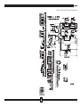
Power
setting –
watts
displayed
on the front
panel
200
180
Desired
Power
160
140
180
120
100
80
90
60
40
20
35
0
0
500
1000
1500
Voltage
sampled
450,000
times per
second
Calculate
measured
resistance
Current
sampled
450,000
times per
second
Calculate
measured
power
2000
Compare
Adjust
output
waveform
(power)
Patient
Measured
Power
Figure 3.1 RF Controller Block Diagram
to optimize the electrosurgical output waveform.
Finally, the RF Controller minimizes RF leakage
currents using the CONMED Leakage Abatement
System (CLAS™), which imposes a duty cycle on
the electrosurgical output when sensed impedance
and output voltage exceed settings-based impedance thresholds and voltage limits in the Coag
modes.
The RF Monitor is also a DSP, but it is used to
monitor the system for a variety of conditions that
could lead to safety problems, including:
• The Monitor has independent sensors for output voltage and current, which it uses to calculate power for comparison with the power
that the RF Controller senses and for comparison with the generator power setting.
• To ensure that the correct outputs are activated, the Monitor also independently
senses current at each of the outputs, looking for current flow that would indicate
electrosurgical power at outputs other than
the selected output.
• The Monitor senses the voltage at the output
of the HVPS to ensure that it is reasonable
for the power setting.
• The Monitor senses the audio output to ensure
that a tone occurs whenever electrosurgical
outputs are active.
• The RF Amplifier drive signal is sensed by
the Monitor to detect improper frequencies
or improper pulse sequences for the selected
mode.
• The Monitor independently compares the
activation signal with that seen by the System
Controller to ensure that the activation signal
is consistent.
The Monitor has the capability to independently
disable the electrosurgical output if a problem is
detected.
The System Controller provides the primary control interface to the user and other outside systems, including the serial interface, the activation
relay, tone generation, and displays.
Finally, the Display accepts all user input and provides all user feedback. The Display is controlled
by the System Controller through a serial interface
and illuminates the LED display elements in a
time division multiplexed fashion; the illuminated
LED display elements are actually on less than half
the time. The Display also provides for user input
through the buttons on the control panel, including switch de-bouncing and conditioning.
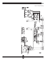
Figure 3.2 illustrates the key elements of the system in block diagram form.
3.2.1
High Voltage Power Supply (HVPS)
The HVPS is comprised of a Power Factor
Control (PFC) section and a Forward Converter
(FC) section. The PFC converts Mains power
to approximately 400 volts using techniques
that ensure the mains current into the supply is
sinusoidal and in phase with the mains voltage.
By doing so, RMS current and harmonic distortion are reduced. The Forward Converter then
3-3
Keyboard
Modes / Power
Activation
Request
Indicators:
Power, Mode,
& bipolar
current
Displays
Activation Relay
Connector Serial Interface
Connector
ACT RLY
RS232
SPI
Real Time
Clock (5K)
AL TONE
ACT TONE
BIP TONE
System
Controller
RF Output
Board
VARM
Mon
RLY DRV
Bip
RF
Transformer
Board
RF INH
PFC EN
RF BP IS
RF BP VS
Mon
RF MP IS
RF MP VS
Host
Bus
Patient
RF Amp
WFORM
RF Controller
Tone
Mon
RFHVSup
DAMP
CNTL
HV Power
Supply
HV SET
WF EN
/HV EN
RF Monitor
MRF MP ISN
MRF MP VSN
M HVDC
MRF BP ISN
MRF BP VSN
MRF H1 SN
MRF H2 SN
MRF FT SN
Figure 3.2 System Block Diagram
converts the PFC output to an adjustable DC
voltage for use by the RF amplifier.
The System Controller can enable or disable the
PFC section of the HVPS. The PFC is normally
enabled during operation to ensure a resistive load
is presented to the Mains.
The Forward Converter is a switch-mode power
converter that adjusts its operating frequency
between 25KHz and 100KHz to ensure proper
resolution for the commanded output voltage. Isolation between Mains power and the
3-4
HVPS output occurs in the Forward Converter.
Forward Converter output voltage is set from the
RF Controller by the /HVSET signal. The RF
Monitor enables the output of the HVPS. The
forward converter includes current limiting on the
output and has provisions to shutdown when the
output of the Low Voltage Supply exceeds limits.
3.2.2
RF Amplifier and Transformer
The RF Amplifier and Transformer portions use
a switch-mode resonant amplifier to convert the
power from the HVPS to the RF energy neces-
sary for electrosurgery. One may think of the
amplifier as a high-speed switch that pulses current through a resonant circuit, which is formed
by the monopolar or bipolar transformer together
with capacitors and inductors connected to the
transformer primary and secondary windings.
Two Metal-Oxide-Semiconductor Field Effect
Transistors (MOSFETs) are connected in a parallel fashion provide the switching. The pulses to
drive the gates on the MOSFETs in this arrangement come from the RF Controller. Adjusting
the width of the drive pulses regulates the output
power in this arrangement; as the pulses become
longer, the output power increases. As noted in
the RF Controller discussion, the RF Controller
compares the output power with the desired
power and adjusts the pulse width to minimize
the difference.
A drive of several pulses at a frequency that closely
matches the resonant frequency of the amplifier
characterize Cut, Blend, and Pinpoint modes, and
the output pulses substantially correspond to the
drive. Spray and Standard Coag modes, however, are characterized by pulses that occur less
frequently where the amplifier is allowed to “ring”
at its resonant frequency. A damping capability is
provided to enhance the surgical effect by damping the ringing effect for each drive pulse.
The Monitor utilizes sensors implemented on each
electrosurgical output to determine whether current is flowing only to the correct outputs. In the
event that current flows in an output that is not
selected, the Monitor can independently disable
RF.
The System 5000™ output panel connectors are
illuminated to aid visibility in low lighting situations. This illumination is provided by a single
LED on the display board that is distributed to
the receptacles through a fiber-optic bundle.
3.2.4
Activation Command Sensing
Each of the Hand Controlled Accessory receptacles incorporate inputs that are used to sense
an activation command from the user. Each
monopolar hand controlled accessory receptacle
has an input for cut and an input for coag. The
bipolar receptacle incorporates a single activation
input. Each of these five inputs is isolated from
the other electrosurgical outputs and from other
low-level circuitry in the system. All are powered
by a multiple output isolated power supply. The
footswitch activation inputs on the back panel are
configured in a similar way and share one of the
isolated power supply outputs.
3.2.5
Automatic Return Monitor (A.R.M.™)
Because the transformer windings and the resonant frequencies between the cut and coag modes
are different, a method of selecting resonating
components is implemented using relays. These
relays switch in the relevant components for the
selected mode based upon commands from the
System Controller.
The patient return connector interfaces to single
and dual dispersive electrodes using a two-pin
connector. A.R.M.™ circuitry uses an actively
driven impedance measurement circuit, which
allows the System Controller to detect the type
of dispersive electrode connected and verify its
integrity.
A Balun transformer is provided for the
monopolar modes to reduce differences between
the source and return currents, thus reducing RF
leakage.
3.2.6
Finally, the RF Amplifier and Transformer provide
capabilities for sensing RF output current and
voltage. These are transformer-isolated representations of the current flowing in the leads and the
voltage across the output, which are supplied to
the RF Controller and the Monitor processors.
3.2.3
Electrosurgical Outputs
Relays are provided to isolate electrosurgical outputs and select which outputs are active. The
System Controller selects the appropriate output
relays based upon activation command inputs.
Low Voltage Power Sources
The low voltage power supply is a medical-grade
universal input offline triple output switching
power supply. The power supply is active anytime
Mains power is connected to the unit with the
Mains power switch turned on.
3.2.7
System Controllers and Monitor
Three processors are used for system interface &
control, RF control, and system monitor functions. The ESU control section consists of dual
channel architecture with two independent channels where one is used exclusively for RF output
control and the other is used for safety monitoring. All three of these processors are located on
3-5
the Control board, along with circuitry to isolate
them from RF noise.
• System Controller (System Microcontroller):
A dedicated microcontroller that handles the
entire user interface, Serial Interface, real
time clock functions, and enables/disables the
power factor control section of the HVPS
using the PFC_EN signal. The System
Controller can also disable the signal used to
drive the RF Amplifier and can terminate RF
drive at any time without interaction from
either the RF Controller or the Monitor. The
System Controller is comprised of an standard
architecture microprocessor together with
Field Programmable Gate Array (FPGA),
which provides interface logic to a variety of
signals, a 3.68MHz oscillator, independent
voltage regulators, a processor supervisory
reset circuit, and other interface logic.
• RF Controller: A DSP that is dedicated to
the output and control of RF power using
the DAMPCNTRL and RF_DRV outputs.
To reduce the effects on the microprocessor circuits on the Controller board from
RF noise at the output, DAMPCNTRL and
RF_DRV are both differential mode signals
running between the RF Controller and the
RF Amplifier. The RF Controller is capable
of disabling RF output power and putting the system into a safe state without any
interaction from the Monitor or the System
Controller. The RF Controller independently monitors the RF output voltage and
current for control purposes through several
scaled inputs. It sets the output voltage of the
HVPS using the HV_SET signal dependent
on the output Mode and power selected. The
RF Controller controls the fan based upon
temperature measurements supplied from the
RF Amplifier through the System Controller.
The RF Controller is comprised of a DSP,
together with circuitry necessary for converting the signals used for control purposes
between analog and digital form, independent
voltage regulators, and other interface logic.
• RF Monitor: A DSP that is dedicated to safety
monitoring activities. The Monitor is capable
of disabling RF output power and putting the
system into a safe state without any interaction from the RF Controller or the System
Controller. To ensure that the Monitor can
correctly perform its function, the Monitor is
3-6
resistively isolated from the other two processors and has independent voltage regulation.
The RF Monitor independently monitors a
variety of inputs to detect safety problems
and has control of disable signals for both the
HVPS and RF Amplifier drive. The Monitor
is comprised of the same DSP as the RF
Controller, together with circuitry necessary
for converting the signals monitored between
analog and digital form, an FPGA to provide
interface logic, independent voltage regulators, isolation resistors and other interface
logic.
3.2.8
Low Voltage Power Monitoring
The low voltage power supply is monitored in
hardware and resets the processors if it is out of
range. The microprocessor supervisory device on
the Controller board monitors +5V and +3.3V
and will reset the system should the levels drop
approximately 0.3V. The Controller assembly
has the circuit that will reset the system should
the 3.3V supply exceed 3.6V. The High Voltage
power supply has a circuit that will inhibit HVDC
should the +5V supply exceed 5.7V.
3.2.9
Operator Control Panel
Keyboard: The main operator input device for
choosing operating modes and settings is the
membrane keyboard panel. Tactile-feedback
mechanical switches allow the operator to set
modes and adjust power settings.
Display Panel: Consists of 7-segment displays,
discrete dual colored LED’s, and light bars that
will display all controls and settings. LED display
elements are illuminated in a time division multiplexed fashion; the illuminated LED display elements are actually on less than half the time.
Bipolar Current Meter: The System 5000™
has a bargraph display that provides an indication of measured bipolar impedance. A special
tone works in conjunction with this bargraph to
indicate when the measured bipolar impedance
exceeds a particular limit.
3.2.10 Activation Tones
Tone is generated for all activation requests, fault
detection and changes made on the Control Panel.
The System Controller generates the tone signal
(ACT_TONE, AL_TONE, & BP_TONE), which
is amplified by a driver on the Backpanel PCB
Assembly. The activation tone and bipolar tone
are individually adjustable, but alarm tones are
not adjustable and are set to generate tone greater
than 65 dB.
Circuitry on the Backpanel PCB permits the
Monitor to verify the oscillation from voltage
measured across the speaker, which provides
confirmation that the speaker is indeed generating audible tones during activation. RF output
is inhibited should the speaker drive current be
absent or too low.
3.2.11 Activation Relay Connector
There is an Accessory Relay Connector, which
provides a relay closure (SPST switch) that may
be used for activating external accessories such as
smoke evacuation units.
3.3
Optional System Configurations
An eight-position configuration dipswitch (S2),
located on the Controller PCB Assembly (A4)
allows a qualified service technician to change
some of the factory default settings. With the
exception of the DACview switch, the configuration dipswitch settings are only detected when
power is initialized, so any changes to the switch
positions must be made with the main power
off. Each switch is OFF in the Down position
and ON in the UP position. The system detects
changes in the DACview switch while power is
on, so it is treated differently. Relevant information for the configuration dipswitches appears in
Section 4.9.
3-7
This page has been intentionally left blank.
3-8
TM
Maintenance
Section 4.0
This section contains information useful in the
maintenance and repair of the System 5000™.
WARNING: High voltages are present at the
connections and within the System 5000™.
Maintenance personnel should take precautions
to protect themselves. Read the safety summary in Section 1.1.4 before working on the
ESU.
4.1
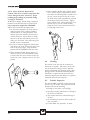
4.3.1
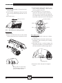
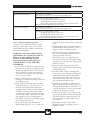
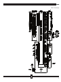
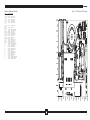
Top Cover Removal and Replacement
Top Removal:
1) Remove the two screws located on rear of
unit as shown.
2) Pull back and up to remove top.
Cover Screws
General Maintenance Information
Cover
Screws
Although the System 5000™ has been designed
and manufactured to high industry standards, it is
recommended that periodic inspection and performance testing be performed to ensure continual
safe and effective operation.
Ease of maintenance was a primary consideration
in the design of the System 5000™. Maintenance
features of this unit include microprocessor aided
troubleshooting aids and push button calibration,
built in fault detection, circuit protection, and easy
access to circuitry while the unit is operational.
These features, coupled with the warranty, local
support, loaner equipment, factory support, toll
free phone service to the factory and available factory training ensure the user of a minimal maintenance effort with extensive support available.
4.2
Maintenance Personnel
Only qualified biomedical engineers should perform service on the System 5000™. Refer all
servicing to a qualified biomedical engineer. If
necessary, your CONMED sales representative will
be happy to assist you in getting your equipment
serviced.
4.3
Cover
Screws
Side Clips
Assembly Breakdown/Parts Access
CAUTION: This device contains components that can be damaged by static electricity.
Proper handling by grounding of personnel
during servicing is mandatory.
Following are instructions for unit disassembly
and reassembly instructions.
4-1
Top Replacement:
1) Place top approximately ¾” from front bezel
on top of unit.
2) Press forward, aligning lip of front bezel with
groove in top and side clips with tabs on casting.
3) Re-install screws.
3) Unlatch display ribbon cable, dispersive electrode connector, ReadiPlug™ cable connector
and two ground connectors.
4) In most situations, it is not necessary to
remove the four power switch connectors.
The bezel can be rotated off to the right side
for output board removal. To fully remove the
bezel, these connectors must be disconnected.
AC Power Switch
Slide top forward.
White
Blue
4.3.2
Black
Brown
Bezel Removal and Replacement
Bezel Removal:
1) Remove Top.
2) Remove two flat-head screws on side of bezel
and two pan-head screws on bottom of bezel.
Bezel Replacement:
1) Connect power switch connectors as shown,
if required.
2) Connect dispersive electrode connector and
ReadiPlug™ cable connector prior to sliding
bezel into place.
3) Slide bezel into unit. As shown in figure, the
output board insulator is positioned between
the sheet metal base and the Output Board.
Insulating Sheet
4) Reconnect cables and replace and tighten
screws.
Spring contacts are exposed and
can be deformed, causing erratic
operation. Handle with care.
4-2
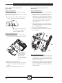
4.3.3 Processor Board Removal and
Replacement
Processor Board Removal:
1) Remove Top.
2) Loosen the two screws holding the board to
slots in the brackets.
3) Unlatch the ribbon cable going to the display.
4) Pull board up and out of unit.
3) Unlatch the ribbon cable and power cable on
the top of the board.
4) Pull board towards inside of unit so screws
line up with keyholes, then up and out of
unit. The power cable to RF Amp must be
unplugged to completely remove transformer
board.
Processor Board Replacement:
1) Align board into the two slots of the brackets
attached to the heatsinks. Align with connector on Output Board and press firmly to
engage it fully. Tighten the two screws.
4.3.4 Transformer Board Removal and
Replacement
Transformer Board Replacement:
1) Reverse board removal operation.
NOTE: When servicing unit, board can be supported in heatsink as shown. This will provide
access to the lower boards while the unit is functional.
Transformer Board Removal:
1) Remove Top.
2) Loosen the two screws mounting the board
to the keyhole slots on standoffs and two
screws mounting the board to the heatsink.
Align slot
in board
with rib on
heatsink.
Route cable through slot.
4-3
4.3.5 Output Board Removal and
Replacement
4.3.6 RF Amp Board Removal and
Replacement
Output Board Removal:
RF Amp Board Removal:
1) Remove Top, Bezel and Processor Board.
Note: It is not necessary to remove power switch
connections from the bezel.
2) Remove the seven cables along the rear side
of the board and the three screws shown.
1) Remove Top, Bezel and Transformer Board.
2) Remove the four screws that attach the
heatsink to the sheet metal chassis. One for
the handle, one on the back panel, and two
below the heatsink. Remove the two screws
that attach the board to the sheet metal chassis as shown. Note: These screws are in
holes, not slots.
3) Unlatch three cables – two cables from the
RF Output Board and a cable from the RF
Power Supply Board.
4) Loosen the smaller hex standoff.
Spring contacts are exposed and
can be deformed, causing erratic
operation. Handle with care.
5) Slide RF Amp Board with heatsink off the
base as shown.
Output Board Replacement:
1) Prior to replacing board, assure that the insulator sheet is positioned properly as shown.
Note: The insulator
sheet provides an
important dielectric
barrier. For safe
operation, position
over center standoff as
shown.
2) Replace board on standoffs.
3) Route cables as they were prior to removal
and connect them back to their proper connectors.
4) Replace and tighten the three screws.
4-4
RF Amp Board Replacement:
1) Slide board with heatsink back into its previous position on the sheet metal chassis. The
heatsink has two pins that align into holes on
the sheet metal chassis.
2) Tighten hex standoff onto board. It provides
an electrical ground to Transformer Board.
3) Reinstall and tighten the six screws and latch
the three cables.
4.3.7 Low Voltage Power Supply Module
Removal and Replacement
NOTE: This module is not user serviceable at
the component level. If faulty, the entire circuit board must be replaced. Replacements are
available from CONMED Customer Service.
Do not discard the module cover, mounting plate and hardware; the replacement part
includes only the circuit board.
Low Voltage Power Supply Module Removal:
1) Remove Top Cover.
2) Loosen four screws located in slots and
unlatch the two cables.
3) Slide Low Voltage Power Supply Module
inward off the slots, then upward to remove.
Circuit Board
NOTE: When servicing unit, board can be held in
heatsink as shown. This will provide access to the
lower boards while the unit is functioning.
4) Remove the cover by removing four screws.
Then remove the four standoffs to separate
the Low Voltage Power Supply from its
mounting plate.
Low Voltage Power Supply Module Replacement:
1) Replace Low Voltage Power Supply on
mounting plate, fasten standoffs, replace cover
and tighten screws.
2) Place Low Voltage Power Supply Module
into unit on standoffs. Tighten the loose
screws and latch the two connectors.
4-5
4.3.8 High Voltage Power Supply Removal
and Replacement
High Voltage Power Supply Board Removal:
1) Remove Top Cover. Position Transformer
Board in its servicing position to gain access
to screws. If desired, remove the Low
Voltage Power Supply.
2) Unlatch the Mains Power Cable, RF Amp
Cable, and Output Board Ribbon Cable.
3) Loosen the two screws holding the edge of
the board to the chassis.
Note: Observe the position of the insulating sheet
under the High Voltage Power Supply. If the
insulating sheet is removed, replace it as shown.
It is important to maintain its function as a
dielectric barrier and to protect the ribbon cable
from the leads of the High Voltage Power Supply
Board.
Insulating Sheet
4) Remove the screw to the handle, the screw to
the back panel, the two screws on the bottom
of the heatsink and slide out the heatsink with
the board attached.
4.3.9 Rear Panel with Board Removal and
Replacement
Rear Panel with Back Panel Board Removal:
High Voltage Power Supply Board Replacement:
1) Remove Top Cover.
2) Unlatch the Ribbon Cable.
3) Remove the four screws on the bottom of the
Rear Panel, and the three screws shown on
the Rear Panel.
1) Slide board with heatsink back into its previous position on the sheet metal chassis. The
heatsink has two pins that align into holes on
the sheet metal chassis.
2) Reinstall and tighten the six screws and latch
the three cables.
4) Slide the Rear Panel with Back Panel Board
back toward the handle and then down to
remove.
4-6
Rear Panel with Back Panel Board Replacement:
1) Slide Rear Panel with Back Panel Board back
into place on the unit.
2) Reinstall and tighten the seven screws and
latch the ribbon cable.
4.3.10 Back Panel Board Removal and
Replacement
Back Panel Board Removal:
1) Remove Top Cover and Rear Panel.
2) Unlatch the Activation Relay and Fan connectors.
3) Remove the four screws for the foot switch
connectors, the two nuts on the volume
potentiometers and the two screws to the rear
panel sheet metal standoffs. This will free the
Back Panel Board from the Rear Panel.
7) Remove the Display Controller Board by separating it from the display board and pulling
it off the studs. There are two 40-pin connectors between these boards that may require
separation by prying with a blunt object.
8) Remove the five hex standoffs and pull the
Display board off the studs.
Display Boards Replacement:
Back Panel Board Replacement:
1) Install Back Panel Board to Rear Panel
2) Reinstall and tighten the six screws, two nuts.
Latch the RSA and fan cables.
Caution: When reinstalling Boards and display
shield, take care to route fiber optic cable as
shown to avoid crimping it between the bezel
and display shield.
4.3.11 Display Boards Removal and
Replacement
Display Boards Removal:
1) Remove the Top Cover and Bezel.
2) Remove 8 nuts and two ground cables on the
back of the display shield.
3) Disconnect the ribbon cable and remove the
sheet metal display shield.
4) Slide the round spacers off their studs.
5) Disconnect the flex circuit connector.
Caution: The flex circuit has a short service
loop and is fragile; handle with care.
6) Pull to disconnect the fiber optic cable from
LED. Caution: The fiber optic cable is fragile; handle with care.
1) Reinstall boards in the reverse order described
above. Latch the flex circuit connector, press
fiber optic cable onto the LED and press the
Display Controller Board firmly into place on
the two 40 pin connectors.
4-7
4.3.12 Power Transistor Replacement
Caution: This device contains components that
can be damaged by static electricity. Proper
handling by grounding of personnel during
servicing is mandatory.
All RF Power Supply and RF Amp components
mounted to the heatsink may be replaced. Use
only components supplied by CONMED.
Follow these instructions for replacement:
1) No thermal compound is necessary, but the
mating surfaces of the transistor, insulator
pad and surface of casting should be clean.
Always replace the insulator pad associated
with the transistor. Always fasten or clamp
the part to the heat sink surface prior to soldering it to the board. This will assure good
thermal contact is maintained.
4) When installing the RF Power Supply transistors or diodes, replace components as shown
and ensure the insulating tube is installed over
the clip. Locate the part on the clip so that
the bend of the clip is approximately centered
on the body of the part as shown. Tighten
screw to 8-10 in-lbs. When tightening screw,
hold the clip to prevent it from rotating.
Clamp the part to the heatsink surface prior
to soldering to the board.
2) In order to maintain alignment with the heat
sink surface, the leads of these parts have been
bent to the proper shape. They should be
purchased from CONMED with bent leads.
3) When installing the RF Amp transistors or
diodes, be sure to orient the Bellville washer
as shown with the convex surface next to the
head of the screw. Tighten screws to 5-7 inch
pounds.
4.4
Cleaning
The interior of the unit may be vacuumed or
blown out as required. The exterior of the unit
may be cleaned by wiping it with a cloth that
has been dampened (not dripping) with a mild
detergent such as Windex® or Formula 409®.
Windex® is a registered trademark of the S.C.
Johnson Company. Formula 409® is a registered
trademark of the Clorox Company.
4.5
Periodic Inspection
The System 5000™ should be visually inspected
at least every six months. This inspection should
include checks for the following:
1) Damage to the power cord and plug.
2) The proper mating and absence of damage to
the accessory connectors.
3) Any obvious external or internal damage to
the unit.
4) An accumulation of lint or debris within the
unit or heatsink.
5) Control Panel cuts, punctures, or dents.
4-8
4.6
Periodic Performance Testing
4.6.3
The System 5000™ should be tested for correct
performance at least once every year. Every unit
is supplied with a serialized Production Test Data
Sheet that tabulates the results of the factory tests
that were performed on the unit. This data is
supplied so that it may be used as a reference for
subsequent tests. Recommended periodic performance tests are listed in the following sections.
4.6.1
Chassis Ground Integrity
Connect a standard ohmmeter between the
earth ground prong on the power plug and the
Equipotential Ground Connection. Compensate
for lead resistance. Confirm less than 0.2 ohms
resistance is measured.
4.6.2
Displays, Alarms and Commands
Perform the Preliminary Functional Test procedure
described in section 2.3.1 of this manual to verify
proper operation of displays, alarms and commands.
Output Power
1) Equipment Requirements:
a) Monopolar Footswitch
b) Bipolar Footswitch
c) Commercial ESU Tester (e.g. Dynatech
454A or equivalent) with 50 and 300
ohm loads for bipolar modes and a 500
ohm load for monopolar modes.
Note: Micro Bipolar is particularly sensitive to the
load resistance. A 50 ohm load should be used for
checking power to obtain the best results.
2) Use test leads to connect the ESU tester to
the unit’s return electrode output and the
footswitch controlled active output. Set the
Load resistance per mode as indicated in
Tables 4.1 and 4.2.
3) Perform the monopolar power tests indicated
in Tables 4.1 and 4.2. The acceptance range
is given in both Watts and Amps to accommodate available test equipment. It is not necessary to test for both power and current.
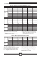
Table 4.1 Monopolar Cut Mode RF Output Power Accuracy
Mode
Load (ohms) Power Setting
Watts (min)
Watts (max)
Amps (min)
Amps (max)
Pure
500
10
7
13.0
0.118
0.161
Standard
500
20
17
23.0
0.184
0.214
500
50
45
55
0.300
0.332
500
100
90
110
0.424
0.469
500
200
180
220
0.600
0.663
500
300
270
330
0.735
0.812
500
10
7
13.0
0.118
0.161
500
20
17
23.0
0.184
0.214
500
50
45
55
0.300
0.332
500
100
90
110
0.424
0.469
500
200
180
220
0.600
0.663
500
10
7
13.0
0.118
0.161
500
20
17
23.0
0.184
0.214
500
50
45
55
0.300
0.332
500
100
90
110
0.424
0.469
500
200
180
220
0.600
0.663
500
10
7
13.0
0.118
0.161
500
20
17
23.0
0.184
0.214
500
50
45
55
0.300
0.332
500
100
90
110
0.424
0.469
500
200
180
220
0.600
0.663
Blend 1
Blend 2
Blend 3
4-9
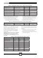
Table 4.2 Monopolar Coag Mode RF Output Power Accuracy
Mode
Load (ohms) Power Setting
Watts (min)
Watts (max)
Amps (min)
Amps (max)
Spray
500
10
7
13.0
0.118
0.161
500
20
17
23.0
0.184
0.214
500
50
45
55
0.300
0.332
500
80
72
88
0.379
0.420
500
10
7
13.0
0.118
0.161
500
20
17
23.0
0.184
0.214
500
50
45
55
0.300
0.332
500
100
90
110
0.424
0.469
500
120
108
132
0.465
0.514
Standard
Mode
Load (ohms) Power Setting
Watts (min)
Watts (max)
Amps (min)
Amps (max)
Pinpoint
500
10
7
13.0
0.118
0.161
500
20
17
23.0
0.184
0.214
500
50
45
55
0.300
0.332
500
100
90
110
0.424
0.469
500
120
108
132
0.465
0.514
500
10
7
13.0
0.118
0.161
500
20
17
23
0.184
0.214
500
60
54
66
0.329
0.363
500
10
7
13.0
0.118
0.161
500
20
17
23
0.184
0.214
500
40
36
44
0.268
0.297
Standard
pulse
Spray pulse
4) Disconnect the ESU tester from the unit.
6) Perform the bipolar power tests indicated in
Table 4.3. This table only provides the minimum number of points to be tested.
5) Use test leads to connect the ESU tester to
the Bipolar Accessory outputs.
Table 4.3 Bipolar Mode RF Output Power Accuracy
Mode
Load (ohms) Power Setting
Watts (min)
Watts (max)
Amps (min)
Amps (max)
Macro
Bipolar
300
10
7
13.0
0.153
0.208
300
20
17
23.0
0.238
0.277
300
50
45
55
0.387
0.428
300
90
81
99
0.520
0.574
50
10
7
13.0
0.374
0.510
50
25
22
28.0
0.663
0.748
50
50
45
55
0.949
1.049
Micro
Bipolar
4.6.4
RF Leakage Measurement
RF Leakage can present a hazard in the operating
room because electrosurgical currents can flow
to the patient and operating room staff through
unintended paths, which can cause injury. RF
4-10
leakage occurs because the total energy in the
output voltage waveform is provided with a conductive path through stray parasitic capacitance
distributed within the generator and along the
length of the leads. Table 4.4 presents the allowed
RF leakage currents to ground.
Table 4.4 Allowable RF Leakage Current to Ground
MEASURED TERMINAL
ACTIVATED ACCESSORY
MODE
RF LEAKAGE (Ma)
Dispersive Electrode
Coag Footswitch
Standard Coag
< 100
Dispersive Electrode
Cut Footswitch
Pure Cut
< 100
Dispersive Electrode
Left Hand Controlled
Standard Coag
< 100
Dispersive Electrode
Right Hand Controlled
Standard Coag
< 100
Footswitched Active
Coag Footswitch
Standard Coag
< 100
Left Hand Controlled Active
Left Hand Controlled
Standard Coag
< 100
Right Hand Controlled Active
Right Hand Controlled
Standard Coag
< 100
Bipolar Right
Bipolar Footswitch
Bipolar Macro
< 67
Bipolar Left
Bipolar Footswitch
Bipolar Macro
< 67
Equipment:
• ESU Tester with RF Leakage function -OR• 0-250 mA RF Ammeter with a 200 ohm 10
W Non-inductive Resistor
• Patient Plate Adapter Plug
• 2 - Test leads, 1 m max. length
• 3 - Test leads, 10 cm max. length
• Wooden table approximately 1 m from floor.
NOTE: The CONMED Leakage Abatement
System (CLAS™) controls RF leakage by pulsing the output to reduce the RMS voltage during
open circuit conditions, thus keeping the hazardous energy below IEC safe limits. Use a measuring device that meets IEC specification for RMS
measured over one second.
Procedure:
1) Ensure that the unit is fully assembled and all
fasteners are tight.
2) Place the ESU tester or meter with resistor on
the table so that they are at least 0.5m away
from the unit under test and any other conductive surface.
3) Set the unit for full power for the modes
noted in the table. Connect the ESU tester in accordance with the manufacturer’s
instructions -OR- connect the 200-ohm noninductive resistor in series with the 250 mA
RF ammeter to the Equipotential Ground
Connection on the Rear Panel. Also make
sure there are no connections to any output
other than the one you are measuring.
WARNING: HAND CONTROL
ACTIVATIONS SHOULD BE KEYED
USING 3” OR LESS WELL-INSULATED
JUMPER. USE OF AN INSULATING ROD
TO INSERT THE JUMPER IS ADVISED
TO PREVENT RF BURNS.
3) One at a time, connect test setup to each RF
output terminal indicated in Table 4.4 and
activate the unit using the corresponding
command. Confirm no meter readings exceed
the specified maximum. Hand control coag
activations are accomplished by connecting a
jumper between the left jack and center jack
of the desired hand switched accessory jack.
RF leakage should also be measured between inactive outputs and the Dispersive Electrode connection. The procedure is as follows:
1) Set the unit for full power for the modes
noted in Table 4.5. Connect the ESU tester
according to manufacturer’s instructions OR- the 200-ohm non-inductive resistor in
series with the 250 mA RF ammeter to the
Dispersive Electrode connection on the front
panel. Also make sure there are no connections to any output other than the one you
are measuring.
2) One at a time, connect this series combination to each RF output terminal indicated
in Table 4.5 and activate the unit using the
corresponding command. Confirm that no
meter readings exceed the specified maximum.
4-11
Table 4.5 Allowable RF Leakage Current - Inactive Monopolar Outputs
MEASURED TERMINAL
ACTIVATED ACCESSORY
MODE
RF LEAKAGE (Ma)
Footswitched Active
Left Hand Controlled
Standard Coag
<50
Footswitched Active
Right Hand Controlled
Standard Coag
<50
Footswitched Active
Bipolar Footswitch
Bipolar Macro
<20
Left Hand Controlled Active
Right Hand Controlled
Standard Coag
<50
Left Hand Controlled Active
Bipolar Footswitch
Bipolar Macro
<20
Right Hand Controlled Active
Bipolar Footswitch
Bipolar Macro
<40
Bipolar Left
Right Hand Controlled
Standard Coag
<48
Finally, RF leakage should be measured between
the inactive bipolar outputs while a monopolar
accessory is activated. Do the following:
according to manufacturer’s instructions -ORthe 200-ohm non-inductive resistor in series
with the 250 mA RF ammeter between the
two bipolar output connections.
1) Set the unit for full power for the bipolar
mode noted in Table 4.6. Connect ESU tester
2) Activate and verify the limit in Table 4.6.
Table 4.6 Allowable RF Leakage Current - Inactive Bipolar Outputs
MEASURED TERMINAL
ACTIVATED ACCESSORY
MODE
Bipolar Right to Left
Right Hand Controlled
Standard Coag
4.6.5
Line Frequency Leakage
These tests are performed most conveniently using
any good quality biomedical electrical safety tester.
Procedure:
1) Connect the electrical safety analyzer to make
the measurements indicated in Table 4.7.
Circuit ground and the Neutral (Low MAINS)
must be connected together for UUT MAINS
leakage testing.
2) Mode: Measure leakage for Bipolar to Neutral
and Chassis to Neutral.
WARNING: Electrocution Hazard. DO NOT
DISCONNECT circuit ground from Earth
Ground unless an isolated MAINS power supply is used.
Table 4.7 Line Frequency Allowable Leakage - Inactive
LINE
GND
LIMIT max
Equipotential Ground
Normal
Closed
30 µA
Equipotential Ground
Reversed
Closed
30 µA
Equipotential Ground
Normal
Open
270 µA
Equipotential Ground
Reversed
Open
270 µA
Dispersive Electrode
Normal
Closed
15 µA
Dispersive Electrode
Reversed
Closed
15 µA
Dispersive Electrode
Normal
Open
15 µA
Dispersive Electrode
Reversed
Open
15 µA
Bipolar Output*
Normal
Closed
15 µA
Bipolar Output*
Reversed
Closed
15 µA
Bipolar Output*
Normal
Open
15 µA
Bipolar Output*
Reversed
Open
15 µA
*Measure the Bipolar Output with Bipolar connections shorted together.
4-12
<48
Equipment:
CAUTION: To prevent RF current from destroying the test equipment and/or affecting leakage
readings, set all power settings to zero.
RF output to Neutral
RF LEAKAGE (Ma)
5) Since the System 5000™ monopolar active
outputs are disconnected by relays when the
unit is not activated, active-to-neutral leakage
tests must be performed with the unit activated in order to be valid.
6) With all power controls set to zero, measure
the leakage current as in step 1 from each of
the three active output terminals to neutral;
see Table 4.8; while that output is activated
in Cut by the appropriate footswitch or hand
control jumper. Hand control cut activations
are accomplished by connecting a jumper
between the two outer jacks of where the
handcontrol accessory is plugged into the
unit.
Table 4.8 Line Frequency Allowable Leakage - Active
RF output to Neutral
LINE
GND
ACTIVATION
LIMIT max
Footswitched Active
Normal
Closed
Monopolar Footswitched Cut
15 µA
Footswitched Active
Reversed
Closed
Monopolar Footswitched Cut
15 µA
Footswitched Active
Normal
Open
Monopolar Footswitched Cut
15 µA
Footswitched Active
Reversed
Open
Monopolar Footswitched Cut
15 µA
Left Hand Controlled Active
Normal
Closed
Left Hand Controlled Cut
15 µA
Left Hand Controlled Active
Reversed
Closed
Left Hand Controlled Cut
15 µA
Left Hand Controlled Active
Normal
Open
Left Hand Controlled Cut
15 µA
Left Hand Controlled Active
Reversed
Open
Left Hand Controlled Cut
15 µA
Right Hand Controlled Active
Normal
Closed
Right Hand Controlled Cut
15 µA
Right Hand Controlled Active
Reversed
Closed
Right Hand Controlled Cut
15 µA
Right Hand Controlled Active
Normal
Open
Right Hand Controlled Cut
15 µA
Right Hand Controlled Active
Reversed
Open
Right Hand Controlled Cut
15 µA
4.6.6 Automatic Return Monitor (A.R.M.™)
Check
A.R.M.™ has two specific ranges that will be
tested initially and then the circuit will be tested
to verify that the circuit measures dissipative electrode resistance correctly. For this testing, only a
Decade Resistance Box (DRB) and a dispersive
electrode cable adapter are required. Connect the
DRB to the Dispersive Electrode Receptacle using
the dispersive electrode cable adapter.
A.R.M.™ may be reset by disconnecting the
dispersive electrode connector or adjusting the
DRB above 10K Ohms until the Single and Dual
Dispersive Electrode Status/Alarm Indicators flash
red in alternating fashion. Allow approximately
two seconds after the DRB is changed before
proceeding to the next step in the procedure.
A.R.M.™ indicators not mentioned in the procedure must be off for each test.
Single and Dual Dispersive Electrode Status/
Alarm Indicators flash red in alternating fashion.
2) Dual Electrode Upper Limit: Set DRB to
140 Ohms and verify that the Dual Dispersive
Electrode Status/Alarm Indicator is flashing
Green and a single bar in the Bargraph is illuminated.
3) Dual Electrode Lower Limit: Set the DRB
to 15 Ohms and verify the Dual Dispersive
Electrode Status/Alarm Indicator is flashing
Green and eight bars in the Bargraph are illuminated.
4) Single Electrode Upper Limit: Set the DRB
to 7 Ohms, then reset A.R.M.™ and verify
the Single Dispersive Electrode Status/Alarm
Indicator is Green and not flashing.
1) Dual Electrode Alarm Limit: Set the DRB to
158 Ohms, then connect it to the Dispersive
Electrode Receptacle and verify that the
4-13
4.6.7
Output Coupling Capacitor Check
WARNING: ENSURE ALL POWER
SETTINGS ARE AT 0 WATTS BEFORE
CONDUCTING THIS TEST TO PREVENT
INJURY TO PERSONNEL AND DAMAGE
TO TEST EQUIPMENT.
NOTE: Not all capacitance meters will read properly for this test. The test frequency should be at
or below 1 kHz for best accuracy. The following
meters have been tried successfully: Fluke 189,
Extech 285, Sencor LC75 and HP4284A (1 kHz
setting or below).
1. Connect shorting plug to banana adapter to
the two pin Dispersive Electrode Receptacle.
Use 6” or less test leads to connect a capacitance meter between the shorting plug
adapter and the footswitched ReadiPlug™
Universal Accessory Receptacle.
2. Measure capacitance and confirm it is less
than 0.5 nF.
3. Confirm cut power is set to 0, then activate
and confirm capacitance is between 4.3 and
6.3 nF.
4. Do not activate for this bipolar test. Move
test leads to Bipolar Output Accessory
Receptacles. Confirm capacitance is between
9.6 and 14 nF.
4.7
System Calibration
The System 5000™ is calibrated during manufacture using equipment traceable to National
Institute of Standards & Technology (NIST)
standards and should retain its accuracy for a long
period of time. Recalibrate the generator after
repair or if it performs out of specification. Check
the calibration in normal operating mode and only
perform calibration if errors are identified.
The System 5000™ stores its calibration in nonvolatile semiconductor memory, so the calibration
will be retained without any action on the part of
the user or maintenance staff. Calibration should
be checked in normal operating mode during
annual preventative maintenance to ensure there is
no change. Calibration is required when:
• “Err 140” occurs: An error is detected with
the stored calibration values.
• “Err 143” occurs: One or more modes require
calibration.
4-14
• The Controller board assembly (P/N 616431), the Transformer board assembly (P/N
61-6445), or the Output board assembly (P/
N 61-6461) is replaced.
• Calibration differences are found during preventative maintenance.
4.7.1
Calibration Preliminaries
Calibration on the System 5000™ occurs in
Calibration Operating Mode, which is entered by
setting the system configuration DIP switches on
the Controller board. Set the Calibration system
configuration DIP switch (A4SW2.2) to the ON
(UP) position and the Test system configuration
DIP switch (A4SW2.1) to the OFF (DOWN)
position. Other configuration DIP switch settings
positions will not affect this. See Section 4.9 for
system configuration DIP switch details.
With this configuration set, turn on power while
pressing and holding the Remote Power Control
Key. Release the Key when you hear the 4-tone
sequence. When the Remote Power Control Key
is released, CAL will appear in the Monopolar Cut
Power Digital Display and the software revision
will appear in the Monopolar Coag Power Digital
Display for a few seconds. The display will then
provide an indication of the calibration status:
• “ALL” will appear in the Monopolar Cut
Power Digital Display if the calibration memory is empty.
• “nEr” will appear in the Monopolar Cut
Power Digital Display, where “n” indicates
how many major modes require calibration,
will be displayed if only particular modes
require calibration. All of the minor mode
indicators will be illuminated and the minor
modes needing calibration will flash.
• “[V”, “[0A”, “bP”, or “Pad” will appear in
the Monopolar Cut Power Digital Display to
indicate the major mode when only minor
modes under that major mode require calibration. All of the minor mode indicators will
be illuminated and the minor modes needing
calibration will flash.
• “[V” will appear in the Monopolar Cut Power
Digital Display with the Pure Cut Mode
Indicator illuminated if all modes are calibrated.
Calibration
Set the Calibration System Configuration
Dipswitch on the Controller to the ON position
Turn main power switch on.
888 888 88
Press Remote Power Control Key,
release when tones begin.
CAL rn
ALL
2Er
3Er
Cu
COA
bP
PAd
Press Remote Power Control Key.
Cu 500 P
Press Monopolar Cut Power Adjustment
Keys to select Cu, COA, bP and PAd.
Cu
COA
Press Cut Mode
Scroll Key to select
Pure, Blend 1,
Blend 2 and Blend 3.
Press Coag
Scroll Key to select
Pinpoint, Spray
and Standard
bP
PAd 10
Press Remote Power Control Key
Connect 10 ohm load Two-Pin
Dispersive Electrode Receptacle
Press Remote Power Control Key
Press Bipolar Power Adjustment Key
Connect indicated load
with meter to output
Press Monopolar Coag Power Adjustment Key
Activate.
PAd 150
Press Monopolar Coag Power Adjustment keys to
match power/current to Calibration Target.
Connect 150 ohm load Two-Pin
Dispersive Electrode Receptacle.
Minimum activation 2 seconds, release.
Press Bipolar Power Adjustment
Key.
Press Remote Power Control Key.
Set the Calibration System Configuration
Dipswitch on the Controller to the OFF position
End - Main power
switch off.
Figure 4.1 Calibration Procedure Flow Chart
4-15
For all except the last of these, a single Press
and release of the Remote Power Control Key is
required to proceed past this point on the menu.
After pressing this key, “[V” will appear in the
Monopolar Cut Power Digital Display with the
Pure Cut Mode Indicator illuminated.
4.7.2
Selecting the Mode to Calibrate
Press the Monopolar Cut Power Adjustment Keys
to select the major mode to calibrate as displayed
in the Monopolar Cut Power Digital Display. The
selections are “[V” for Cut, “[0A” for Coag, “Bp”
for Bipolar, or “PAd” for the Dispersive Electrode
A.R.M.™ connection. If any of the minor modes
under these major modes are not calibrated, the
displayed major mode will flash.
Scroll between the monopolar minor modes using
the Cut Mode Scroll Key or the Coag Scroll Key,
as appropriate. Macro Bipolar is used to calibrate
both of the Bipolar modes, so no scrolling is necessary.
4.7.3
Calibrating a Monopolar Mode
This section applies to the Pure Cut, Blend 1,
Blend 2, Blend 3, Pinpoint Coag, Standard Coag,
and Spray Coag modes.
Calibration may be performed by measuring current or by measuring power. To select between
calibration using measured current and measured
power, press the Bipolar Power Adjustment Keys
to set the calibration units to either “A” for current
or “P” for power.
The resistance to be used for calibration will
appear in the Monopolar Coag Power Digital
Display. Connect a resistor of this value between
the output connection that is being used for calibration and both pins on the Two-Pin Dispersive
Electrode Receptacle.
Press and release the Remote Power Control Key
to begin calibration. After this key is pressed, the
target level appears in the Monopolar Coag Power
Digital Display.
Activate using the appropriate Handswitch or
Footswitch. Power will now flow to the resistor. While monitoring either the current or the
power, adjust the power up or down using the
Monopolar Coag Power Adjustment Keys until
the measured value is as close to the target level as
possible. The activation must be maintained for a
minimum of 2 seconds to ensure the calibration is
valid. After the power is properly adjusted, release
4-16
the activation. Press and release the Remote
Power Control Key to complete the calibration
sequence for the selected minor mode.
After a minor mode has been calibrated, the
associated minor mode indicator will quit flashing. When all of the minor modes within a major
mode have been calibrated, the major mode
indicated in the Monopolar Cut Power Digital
Display will quit flashing.
4.7.4
Calibrating Bipolar Modes
The Bipolar modes are calibrated using a method
that is very similar to the Monopolar modes.
Both Bipolar modes are calibrated with a single
calibration of the Bipolar Macro mode.
Calibration may be performed by measuring current or by measuring power. To select between
calibration using measured current and measured
power, press the Bipolar Power Adjustment Keys
to set the calibration units to either “A” for current
or “P” for power.
The resistance to be used for calibration will
appear in the Monopolar Coag Power Digital
Display. Connect a resistor of this value between
the two active connections in the Bipolar
Accessory Receptacle.
Press and release the Remote Power Control Key
to begin calibration. After this key is pressed, the
target level appears in the Monopolar Coag Power
Digital Display.
Activate using the Bipolar Footswitch. Power
will now flow to the resistor. While monitoring
either the current or the power, adjust the power
up or down using the Monopolar Coag Power
Adjustment Keys until the measured value is as
close to the target level as possible. The activation
must be maintained for a minimum of 2 seconds
to ensure the calibration is valid. After the power
is properly adjusted, release the activation. Press
and release the Remote Power Control Key to
complete the calibration sequence for the Bipolar
mode.
After the Bipolar mode has been calibrated, the
Macro Bipolar Indicator and the major mode
indicated in the Monopolar Cut Power Digital
Display will both quit flashing.
4.7.5
Calibrating A.R.M.™
A.R.M.™ is calibrated against a pair of known
resistances.
Press and release the Remote Power Control Key
to begin calibration. The resistance to be used
for calibration will appear in the Monopolar Coag
Power Digital Display. Connect a resistor of this
value ±1% between the two active connections in
the Two-Pin Dispersive Electrode Receptacle.
Calibrate the particular value connected by pressing one of the Bipolar Power Adjustment Keys.
When the value is accepted, a two-tone sequence
will sound and the resistance in the Monopolar
Coag Power Digital Display will quit flashing.
Now scroll to the other of the pair of known
resistances using the Monopolar Coag Power
Adjustment Keys. The resistance to be used for
calibration will appear in the Monopolar Coag
Power Digital Display. Connect a resistor of this
value ±1% between the two active connections in
the Two-Pin Dispersive Electrode Receptacle.
Calibrate the particular value connected by again
pressing one of the Bipolar Power Adjustment
Keys. When the value is accepted, a two-tone
sequence will sound and the resistance in the
Monopolar Coag Power Digital Display will quit
flashing.
Press and release the Remote Power Control Key
to complete A.R.M.™ calibration.
After A.R.M.™ has been calibrated, the major
mode “PAd” indicated in the Monopolar Cut
Power Digital Display will quit flashing.
4.7.6 Completing Calibration
Turn power off and set the Calibration system
configuration DIP switch (A4SW2.2) to the OFF
(DOWN) position. See Section 4.9 for system
configuration DIP switch details. The ESU will
be ready for normal operation the next time the
power is turned on.
4.8
Last Fault Code Retrieval and
Clear
Up to 20 error codes can be stored in memory
for retrieval. Each error code stored is “date
stamped” where the “time” and “date” the error
occurred is also stored for retrieval. When retrieving the error codes, it is also possible to retrieve
the system settings when the error occurred.
4.8.1
Last Fault Code Retrieval
1) Turn the Main power on. While the unit
is powering up, press the PC key until a
tone occurs. This action will place the sys-
tem in the Last Fault Code Mode (LFC).
Electrosurgical outputs cannot be activated
while the system is in LFC.
2) For 3 seconds: “LF[” will be displayed in the
Cut Window, which is for Last Fault Codes.
The Coag window will display “rX”, (where X
is a numeric value for the software revision).
3) If any errors are stored in memory, the Cut
Window will next display “Err”; the Coag
window will display the error code (a numeric
value); and the Bipolar Window will display
the storage location of that error code.
Last Fault display
Pure
Blend 1
Blend 2
Blend 3
err 381
1
4) Scroll through the stored error codes using
the Bipolar Power Adjustment Keys. The
error codes are stored Last in, First out. A
“1” in the Bipolar Display shows the last error
that occurred. Press the Bipolar Up key and
a “2” will be displayed if more than one error
occurred.
5) To retrieve the date and time of the error, it
is necessary to have a Handcontrol accessory
connected. Press the Cut activation switch
and the “time” that the error occurred is displayed. Press the Coag activation switch and
the “date” that the error occurred is displayed.
Press both Cut and Coag activation switches
and the Display Panel will show the system
settings when the error occurred.
Time Display: Press Handcontrol Cut Switch
Hours can be set for A.M. or P.M. The time is
displayed as Hours - Minutes - Seconds.
Pure
Blend 1
Blend 2
Blend 3
2P
23
12
Date Display: Press Handcontrol Coag Switch
The date is displayed as Month - Day - Year.
Pure
Blend 1
Blend 2
Blend 3
09
28
04
4-17
6) If the date defaults to 01 01 01 or the time
defaults to 12P 0 1, then the Real Time Clock
battery is low or the clock was not set on the
last service. The battery voltage must be 2V
or greater for the Real Time Clock to run.
entire fault code memory. The cut window
will display “[Lr” when codes are cleared.
• Pressing the PC key again will display the
optional system configuration settings.
4.9
Displaying Optional System
Configuration
a) The battery is being charged when the
main power is turned on. It takes about
12 hours to charge the battery if the battery is fully discharged.
The optional system configuration DIP switch
settings can be checked without removing the top
cover.
b) To test the battery, connect a DVM to
the battery lead that is visible through the
hole on the display shield (backside of
the Display PCB assembly). Connect the
other lead of the DVM to the GND test
point on the Controller Assembly (TP6).
Test the battery voltage with the main
power turned off. The battery voltage
should be 3V or greater.
• Turn on the main power. While the system is
powering up, press and hold the PC Key on
the Display panel until the Test Tone starts.
• Last Fault Codes are displayed initially. The
Cut window will display “LF[” and the Coag
window will display the software revision
number for approximately 3 seconds, then the
Last Fault Code will be displayed. (See the
section on Last Fault Codes.)
c) Another way to test if the battery is
charged it to set the clock and date. Turn
off the main power and then turn the
main power back on. Press the PC key
while the unit is powering up to enter the
Last Fault Codes. If the clock displays
12P 0 1, then the battery is not charged
or taking a charge.
4.8.2
• Press the PC Key again and the configuration
DIP switch settings will be displayed. “0” is
for OFF and a “1” is for ON.
The eight-position configuration DIP switch (S2),
located on the Controller PCB Assembly (A4)
allows a qualified service technician to change
some of the factory default settings. The default
switch is only read during Power On Self Test
(POST) or when the system is powered on, so
any changes to the switch positions should be
made with the main power off. Each switch is
OFF in the down position and ON in the up
position. Relevant information for each switch is
described in Table 4.9 and the positions are illustrated in Figure 4.2.
Clearing Last Fault Codes
As errors occur, fault codes from earlier errors are
erased in a last-in-first-out fashion. While it is not
absolutely necessary to clear the older codes, clearing the codes may be desirable in some situations.
• Pressing the Monopolar Cut Power
Adjustment Down Key followed by the
Remote Power Control Key will clear the
CUT
COAG
000
2
PCEN
1
SCOAG
N
DCUT
O
LAST
TEST
CAL
101
3
4
5
6
7
8
Figure 4.2 DIP Switch Positions
4-18
BIPOLAR
00
Table 4.9 DIP Switch Settings
Config. Title /
Switch
Display
Position Element
Default
Description for Off
Description for On
1
TEST /
Cut 100’s
Off
Run Mode. Required position for
surgery.
Activates Test Mode, which inhibits most
of the system level monitoring for troubleshooting purposes. When this switch
is ON, the Remote PC Switch on the
Display Panel must be pressed until the
Test Tone begins. If the Remote PC key is
not pressed, and Err 100 is displayed and
the power must be cycled.
2
CAL/ Cut
10’s
Off
Run Mode. Required position for
surgery.
Required for calibration of output power
and A.R.M.TM When this switch is ON,
the Remote PC Switch on the Display
Panel must be pressed until the Test Tone
begins. If the Remote PC key is not
pressed, and Err 100 is displayed and the
power must be cycled.
3
SCOAG /
Cut 1’s
On
Allows simultaneous activation
of two accessories for Pinpoint
Coagulation.
Allows activation of only one accessory for
Pinpoint Coagulation. Spray and Standard
Coagulation modes always allow simultaneous activation of two accessories.
4
DCUT /
Coag 100’s
Off
Allows activation of only one active
accessory in cut modes.
Allows activation of two active accessories
in cut modes.
5
LAST /
Coag 10’s
On
Defaults to Pure Cut, Pinpoint
Coag, and Macro Bipolar and sets
all power levels to zero (0W) each
time the system is initialized.
Defaults all modes and power levels to the
settings the last time the system was powered down.
6
PCEN /
Coag 1’s
Off
Allows the Remote Power Control
feature to be enabled by pressing
the PCEN switch on the Display
Panel.
Inhibits the Remote Power Control feature.
7
Not used
/ Bipolar
10’s
Off
Not used.
Not used.
8
DACview /
Bipolar 1’s
NA
DACview - See below.
DACview - See below.
4-19
4.10
DACview
DACview is a troubleshooting aid that allows
access to internal readings. The feature allows
output voltage, current and power that the system
reads to be output to a DVM or oscilloscope.
To use DACview, the system must be in the Test
Mode.
1) Set the system for operation in Test Mode as
described in the preceding section.
2) Connect a DVM to the Control Board test
points labeled TP7 – DAC_VIEW and TP6
– AGND.
3) Turn the power on and press the PC key until
the Test Tones begin.
4) Move the DACview switch (S2 position 8
– the change is recognized, not whether the
switch is on or off).
Channel
0
1
2
3
4
5
6
7
8
9
10
11
12
13
14
15
16
17
18
19
20
21
22
23
24
25
26
27
4-20
Source
Monitor
Monitor
Monitor
Monitor
Monitor
Monitor
Monitor
Monitor
Monitor
Monitor
Monitor
Monitor
Monitor
Monitor
Monitor
Monitor
Monitor
Monitor
System Controller
Controller
Controller
Controller
Controller
Controller
Controller
Monitor
Monitor
5) The Monopolar Cut Power Digital Display is
used to display the selected DACview channel. Since power was just initialized, the
Monopolar Cut Power Digital Display will
display “0” at this point. Select the desired
channel using the Monopolar Cut Power
Adjustment Keys.
6) Move the DACview switch (again, the change
is recognized, not whether the switch is on or
off). The cut power setting will be displayed.
7) To select a different location to monitor with
a DVM, simply move the DACview switch
and the memory locations will be displayed
instead of the cut power. Select the desired
selection and then move the DACview switch
again.
Table 4.10 DACview Channels
Function
No channel selected
RF RMS Power (300mS running average)
RF RMS Power
RF RMS Current
RF RMS Voltage
RF RMS Current (300mS running average)
RF RMS Voltage (300mS running average)
Max RMS RF Voltage during single activation
Reserved- Future Use
H1 accessory, RMS current output
H2 accessory, RMS current output
FT accessory, RMS current output
BP accessory, RMS current output
+HV, High Voltage power supply output
Max Power during single activation
Max RMS Current during single activation
Calculated output resistance
A/D Input DC voltage offset
Reserved- Future Use
A.R.M.TM resistance
Gate pulse width
Output RMS Voltage
Output RMS Current
Output impedance
Reserved- Future Use
Reserved- Future Use
Calibrated POST RF cut mode voltage
Calibrated POST RF coag mode voltage
Scaling
0.01 V / 1 W
0.01 V / 1 W
1V/1A
0.001 V / 1 V
1V/1A
0.001 V / 1 V
0.001 V / 1 V
1V/1A
1V/1A
1V/1A
1V/1A
0.01 V / 1 V
0.01 V / 1 W
1V/1A
0.001 V / 1 OHM
1V/1V
0.01 V / 1 OHM
Variable
Variable
Variable
0.2V/100 OHM
0.001 V / 1 V
0.001 V / 1 V
4.11
Setting the Clock
The clock is only visible while in the Last Fault
Display and the purpose of the clock is only to
“Date/Time Stamp” system faults.
1) To set the clock, turn the Main power on.
While the unit is powering up, press the PC
key until a tone occurs. This action will place
the system in the Last Fault Code Mode
(LFC).
2) For 3 seconds: “LF[” will be displayed in the
Cut Window, which is for Last Fault Codes.
The Coag window will display “rX”, (where X
is a numeric value for the software revision).
3) If any errors are stored in memory, the Cut
Window will next display “Err”; the Coag
window will display the error code (a numeric
value); and the Bipolar Window will display
the storage location of that error code.
4) Press PC key: the display will show the DIP
switch settings on the Controller Assembly.
5) Press PC key: the “Date” will be displayed
as MO – DAY – YEAR. Press the Power
Adjustment Keys associated with each window to set the date. Once the date is set,
Press the STORE” key that is below the
Program Window scroll key to lock the date
in memory.
6) Press PC key: the “Time” will be displayed as
HOUR – MINUTE – SECONDS. Press the
Power Adjustment Keys associated with each
window to set the time. The Cut Window
has either a “P” for PM. or “A” for AM. Once
the time is set, Press the STORE” key that is
below the Program Window scroll key to lock
the time in memory.
7) Press PC key to return to the error code display. To exit the Last Fault Code Mode, it is
necessary to turn off the main power.
4.12
Troubleshooting
Listed in Table 4.11 are potential errors that
may occur and problem solving ideas for each.
All error codes (Err xxx) can only be cleared by
cycling power. When an error code is displayed,
reset the system to determine if the error can be
cleared with a System Reset or if further service
is required. Error codes are stored as Last Fault
Codes (See Last Fault Codes).
Table 4.11 Troubleshooting
Problem
Possible Cause
Display Panel Blank when System is
Powered on
Verify the power cord is fully seated in the power receptacle on the back of the
System.
With the power cord disconnected, verify fuses are good and are installed properly in the receptacles on the back panel of the generator.
Remove the top cover and verify that the controller board and all harnesses are
properly seated.
Check the Low Voltage Power Supply for +5V and +15V.
Display: A[[ xxx
Accessory error – Faulty accessory is connected, a hand controlled accessory
is erroneously actuated, or a footswitch is erroneously actuated. Ensure that
footswitches are not stacked on top one another. A[[ rH and A[[ LH, indicate
problems with the accessories connected to the right-hand and left-hand Hand
Controlled Monopolar Accessory Receptacles, respectively. A[[ FS indicates a
problem with the footswitch connected to either of the Monopolar or Bipolar
Footswitch Connectors.
Display: A[[ [P xx
Control Panel error – Check for a faulty push button on the front control panel,
a control panel push button that has been pushed while the unit is being turned
on, or a faulty cable connection between the front panel and the display board.
Display: LF[ xxx
Last Fault Codes – the Remote Power Control Key was pressed while power was
initialized. The generator must be reset to clear this condition. See section 4.8.
4-21
Problem
Possible Cause
Display: [al
The system is in the Calibration Mode. Calibration Mode is selected when the
configuration DIP switch in the second position on the Controller assembly is in
the ON (Up) position and the Remote Power Control Key is pressed and held
while power is turned on. See section 4.9.
Display: Err xxx
Refer to Table 4.12 for list of Err codes and possible causes. If an Err code
appears, try cycling power. If it reappears, the unit should be taken out of service
until a qualified biomedical engineer can diagnose the problem.
Single and Dual Dispersive
Electrode Status / Alarm Indicators
flash alternating red.
A Dispersive Electrode is not connected to the system
Flashing Decimal Points on the
Display
The system is in the Test Mode. Test Mode is selected when the configuration
DIP switch in the first position on the Controller assembly is in the ON (Up)
position and the Remote Power Control Key is pressed and held while power
is turned on. Note: When the Test Mode is active, most of the internal safety
monitoring is inhibited. See section 4.9.
No output power
One or more connections inside the system are bad. Check:
• A6J1, controller
• A6J2, monopolar transformer board
• A6J3, high voltage power supply
• A6J4, bipolar output
• A7J1, controller
• A7J2, monopolar output
• Faulty accessory – blade not seated fully
• Output board jacks not making contact
A Dual Dispersive Electrode is connected but is not properly applied to patient.
A Dispersive Electrode is connected to the System, but is not properly seated
– ensure the connector is fully seated in the Two-Pin Dispersive Electrode
Receptacle.
Low voltage power supplied to A6 is bad. Check:
• +15V
• -15V
• -5V
Shorted RF Amplifier power MOSFET.
Note: A better indication of the problem will be provided by cycling power,
which will allow the generator to find a fault during POST.
• Remove A6 JMP1 and A6 JMP2.
• Using an ohmmeter measure between drain and ground on Q3 and Q4 for
low resistance.
• Using an ohmmeter measure between gate and ground on Q3 and Q4 for
low resistance.
• If either exhibit low resistance, either replace the faulty MOSFET or replace
the RF Amplifier.
HVPS output too low.
• Configure system for test mode operation.
• Unplug the connector A6J3 on the RF Amplifier.
• Set the system for Pure cut at 35 watts.
• Activate and ensure A9LED2 is brightly illuminated.
Improper gate drive.
• Configure system for test mode operation.
• Verify that the input to A6U1 is switching between –5V and 0 volts when
the system is activated, and that this signal is synchronous with crossing transitions of RF_DRV and /RF_DRV.
• Verify that A6 GATE_A and A6 GATE_B are at –5V when not activated.
4-22
Problem
Possible Cause
Incorrect monopolar output
Bad calibration – Recalibrate
Ensure the load resistor is correct when checking output power.
Bad voltage or current feedback. Check:
•
A7 RF_MP_VSN, monopolar voltage sense
•
A7 RF_MP_ISN, monopolar current sense
•
These signals should match the Monitor voltage and current sense,
MRF_MP_VSN and MRF_MP_ISN, respectively.
Incorrect bipolar output
Bad calibration – Recalibrate
Ensure the load resistor is correct when checking output power.
Bad voltage or current feedback. Check:
•
A5 RF_BP_VSN, bipolar voltage sense
•
A5 RF_BP_ISN, bipolar current sense
•
These signals should match the Monitor voltage and current sense,
MRF_BP_VSN and MRF_BP_ISN, respectively.
4.12.1 HVPS Troubleshooting Hints
• Danger: Use an isolation transformer when
working on Mains side! A line on the printed
circuit board and on the schematic identifies the
Mains side of the HVPS.
WARNING: LOSS OF POWER SUPPLY
ISOLATION CAN CAUSE ELECTRICAL
SHOCK. WHEN SERVICING THE
HIGH VOLTAGE POWER SUPPLY,
ASSUME INTERNAL ISOLATION IS
COMPROMISED UNTIL VERIFIED
OTHERWISE.
• For best access for HVPS measurements, place
both the Low Voltage Power Supply and the
Transformer Boards in their service positions;
that is, mounted vertically in the appropriate heatsink mounting slots. See mechanical
access section for details.
• Make sure the LED for the circuit you’re
working on is OFF when making connections
or touching circuitry.
•Observe both LEDs during POST. The PFC
LED should always be on when power is on.
It will become momentarily brighter during POST. The Forward Converter LED will
normally be off unless it has been recently
activated. After activation it will slowly fade
to off. During POST, it should turn on dimly,
then brightly, then fade. The brightness of
both LEDs corresponds to the output voltage
of the corresponding circuit.
• Check Line Voltage input, HVSET, MHVEN, PFC_EN, and +15, +5, GND con-
nections for proper operation before replacing
parts.
• If LED2 does not light during POST, unplug
the RF Amplifier and cycle power – there
might be a short on the RF Amplifier.
• If fuses are blown, Q3 is probably shorted.
Also check surrounding components for failure if Q3 is found to be bad.
• If the Forward Converter output will not
exceed about 70Vdc, the PFC output voltage
is probably too low. (This limit will vary with
input line voltage.)
• The Forward Converter gate pulse width
should be close to 50% with no input voltage
while HVSET is low.
•If the PFC output voltage is changing with
heavy load, try increasing mains voltage with
a variable transformer. If this stabilizes the
PFC output voltage, PFC current sense circuitry is probably at fault. This is not generally a problem with 220V inputs.
• The PFC can be disabled for safer low voltage Forward Converter troubleshooting – by
shorting TP11(PFC_EN) to TP4(-HV). Use
a variable transformer to set the desired input
voltage to the Forward Converter.
• Check the clock frequency and reference voltage on both the PFC controller and Forward
Converter controller integrated circuits. The
PFC clock must have PFC enabled to function correctly.
• If the output voltage for either PFC or
Forward Converter is too high, check the
feedback resistors.
4-23
• The Forward Converter will oscillate with brief
output bursts when the output current limit
is active. This is generally caused by shorted
MOSFETS on the RF Amplifier.
• At low output current, the PFC will cycle on
and off. This is normal.
• When replacing a MOSFET, check all the gate
drive components.
• Resistance measured between TP7 and TP4
(-HV) when power is off should be greater
than 100K ohms. Resistance measured
between U2P15 (VCC) and TP4 when power
is off should be greater than 100K ohms.
• If either of above is low, Q3 or the associated
protection diodes are suspect. If these are
removed and the measured resistance continues to be low, U2 is probably failed.
• The forward converter can be disconnected
from the Power Factor Controller for troubleshooting the PFC. Do this by removing the
E1-E2 wire. Be sure to note the routing of
the wire through T1 so it can be reconnected
correctly. Incorrect polarity can damage the
Forward Converter.
4.13
Parts Ordering Information
To obtain replacement parts or additional information regarding your unit, write or telephone
according to the contact information as listed on
the inside front cover of this manual, or contact
your CONMED distributor. To ensure prompt
service, please provide the following information:
Model Number
Serial Number
Reference Designator and Description of Part
Conmed Part Number (if known)
Quantity Desired
Mailing or Shipping Address
Preferred Shipping Means (if any)
Purchase Order Number (if applicable)
Your Name
If you are returning a unit, obtain a Return
Authorization (R.A.) Number from CONMED
Technical Services. Please mark the R.A. number
on the outside of the carton for prompt service.
4-24
4.14
Fault Codes
This section of the manual contains a table of fault
codes. Each numeric fault code is listed along
with a description of the fault, possible causes and
things to check, and corrective actions.
Table 4.12 Fault Codes
Err
Code
Description
Possible Cause
Things to check
Correction
100
Test or CAL mode
dip switch with no
remote power control key press
The Remote Power Control
Key must be depressed
when power initialized
until the test tones sound.
Release this key before the
last tone sounds.
Cycle system power while pressing the Remote Power Control
Key and determine if this error is
repeated.
Replace the
Controller assembly.
101
Controller/Monitor
DIP switch mismatch
The System Controller and
the Monitor do not detect
the same settings for the
Configuration Dipswitches.
Cycle system power and determine if this error is repeated.
Replace the
Controller assembly.
102
Corrupted communications
between the System
Controller and
Monitor
The data transmitted from
the System Controller to the
Monitor through the HPI
port is faulty.
This could be caused by
damage to components
associated with the HPI bus
on the Controller, permitting electromagnetic interference to upset one of the
processors.
Cycle system power and determine if this error is repeated.
Replace the
Controller assembly.
103
Corrupted communications
between the System
Controller and RF
Controller
The data transmitted from
the System Controller to the
RF Controller through the
HPI port is faulty.
This could be caused by
damage to components
associated with the HPI bus
on the Controller, permitting electromagnetic interference to upset one of the
processors.
Cycle system power and determine if this error is repeated.
Replace the
Controller assembly.
104
Monitor TOKEN
not incremented,
monitor program
scrambled
The data transmitted from
the System Controller to the
Monitor through the HPI
port is faulty.
This could be caused by
damage to components
associated with the HPI bus
on the Controller, permitting electromagnetic interference to upset one of the
processors.
Cycle system power and determine if this error is repeated.
Replace the
Controller assembly.
105
Controller failed
ram test
The System Controller
memory errors have been
detected during POST.
Cycle system power and determine if this error is repeated.
Replace the
Controller assembly.
4-25
Err
Code
Description
Possible Cause
Things to Check
Correction
106
RF controller bootload program does
not match controller ROM table
The program transmitted
from the System Controller
to the RF Controller
through the HPI port at
startup is faulty.
This could be caused by
damage to components
associated with the HPI bus
on the Controller, permitting electromagnetic interference to upset one of the
processors.
Cycle system power and determine if this error is repeated.
Replace the
Controller assembly.
107
Monitor bootload
program does not
match controller
ROM table
The program transmitted
from the System Controller
to the Monitor through the
HPI port at startup is faulty.
This could be caused by
damage to components
associated with the HPI bus
on the Controller, permitting electromagnetic interference to upset one of the
processors.
Cycle system power and determine if this error is repeated.
Replace the
Controller assembly.
108
RF TOKEN not
incremented, RF
controller program
scrambled
The program transmitted
from the System Controller
to the RF Controller
through the HPI port at
startup is faulty or has been
corrupted after initialization.
This could be caused by
damage to components
associated with the HPI bus
on the Controller, permitting electromagnetic interference to upset one of the
processors.
Cycle system power and determine if this error is repeated.
Replace the
Controller assembly.
109
Communications
lost during POST
tests
Communications through
the HPI port are faulty.
This could be caused by
damage to components
associated with the HPI bus
on the Controller, permitting electromagnetic interference to upset one of the
processors.
Cycle system power and determine if this error is repeated.
Replace the
Controller assembly.
112
Pre-activation
handshake, monitor
does not read an
activation signal
The activation signals
detected by the System
Controller and the Monitor
do not match.
Cycle system power and determine if this error is repeated.
Replace the
Controller assembly.
4-26
Err
Code
Description
Possible Cause
Things to Check
Correction
113
Pre-activation
handshake, monitor does not read a
tone signal
Prior to enabling
electrosurgical output
power, the Monitor ensures
that an activation tone is
present. This error occurs
if the activation tone is not
present when the Monitor
checks prior to enabling
electrosurgical output
power.
Increase the tone volume by
adjusting the Volume Control on
the back panel of the generator.
Cycle system power and determine if this error is repeated.
Configure system for test mode
operation.
Check the tone drive signal from
the Controller assembly while
the unit is activated. Lack of a
signal indicates a problem with
the Controller assembly.
Check for a proper TONE_
MON signal to the controller. Lack of a signal indicates
a problem with the Back Panel
assembly.
Replace the
Controller assembly.
Replace the Back
Panel assembly.
114
Display or keyboard SPI communication failure
Communication between
the Control assembly and
the Display assembly over
the SPI bus is faulty.
Cycle system power and determine if this error is repeated.
Check SPI_SCK, SPI_MOSI,
and SPI_MISO to see signals
toggle.
Replace the cable
between the Display
and the Controller.
Replace the
Controller assembly.
Replace the Display
assembly.
117
5.0 volt too low
5-volt power in the system
is too low.
Check the output of the low
voltage power supply.
Verify that the ADC reference
voltages on the Controller are
2.5 volts.
If the power supply voltage is out of
limits, replace the
power supply.
If the power supply is within limits, replace the
Controller assembly.
118
5.0 volt too high
5-volt power in the system
is too high.
Check the output of the low
voltage power supply.
Verify that the ADC reference
voltages on the Controller are
2.5 volts.
If the power supply voltage is out of
limits, replace the
power supply.
If the power supply is within limits, replace the
Controller assembly.
122
System Controller
flash program CRC
does not match the
calculated CRC
The self-check CRC for the
System Controller is not
internally consistent, indicating an error in the stored
software.
Cycle system power and determine if this error is repeated.
Replace the
Controller assembly.
135
A.R.M.™ calibration (10/150 Ohm)
EEprom CRC
failed
The CRC for the calibration
coefficient memory is not
self consistent, indicating an
error in the stored calibration coefficients.
Recalibrate the A.R.M.™ system.
See section 4.7.
Replace the
Controller assembly
if the system will not
calibrate.
4-27
Err
Code
Description
Possible Cause
Things to Check
Correction
136
A.R.M.™ circuit
dropped below .4V
(circuit failed)
The A.R.M.™ circuit on
the Output assembly or the
A.R.M.™ sensing circuit on
the Controller assembly has
failed.
Verify proper voltage on the
VARM signal entering the
Controller assembly.
Replace the Output
assembly if VARM
entering the
Controller is faulty.
Replace the
Controller assembly
if VARM appears
correct.
137
RF controller calibration EEPROM
CRC failed
The CRC for the calibration
coefficient memory is not
self consistent, indicating an
error in the stored calibration coefficients.
Recalibrate the entire system.
Replace the
Controller assembly
if the system will not
calibrate.
138
Monitor calibration
EEPROM CRC
failed
The CRC for the calibration
coefficient memory is not
self consistent, indicating an
error in the stored calibration coefficients.
Recalibrate the entire system.
Replace the
Controller assembly
if the system will not
calibrate.
139
During calibration,
not all points were
entered for the
mode
The calibration was not
completed in the correct
manner.
Recalibrate any uncalibrated
modes. See Section 4.7.
Replace the
Controller assembly
if the system will not
calibrate.
140
A calibration
EEPROM CRC
failed (POST
ERROR)
The CRC for the calibration
coefficient memory is not
self consistent, indicating an
error in the stored calibration coefficients.
Recalibrate any uncalibrated
modes. See Section 4.7.
Replace the
Controller assembly
if the system will not
calibrate.
141
Test and cal dip
switches are both
turned on
The Calibration and Test
Configuration Dipswitches
are both in the ON position.
At least one of these must
be in the OFF position.
Change the Calibration and Test
Configuration Dipswitches to
the desired state, cycle system
power, and determine if this
error is repeated.
Replace the
Controller assembly.
142
RF PWM
(RF_PROT) gate
protection circuit
shutdown
The pulse width commanded by the RF Controller
exceeds the maximum
allowed for the selected
mode.
Cycle system power and determine if this error is repeated.
Replace the
Controller assembly.
143
The unit or a mode The system or a mode was
was never calibrated never calibrated.
The Controller was replaced
but not calibrated.
Calibrate any modes that need
calibration.
Replace the
Controller assembly
if the system will not
calibrate.
4-28
Err
Code
Description
Possible Cause
Things to Check
Correction
144
RF controller and
Monitor power levels do not match
The Monitor and RF
Controller and constantly
checking to ensure they see
the same electrosurgical output power during activation.
This error occurs if the
power they sense does not
match. This typically results
from differences between
the independent Monitor
and RF Controller sensing
circuits.
Use DACView to troubleshoot
the Monitor.
Verify that the output power is
consistent with displayed power
setting.
Check voltage and current sensing channels for both the RF
Controller and the Monitor.
Replace the
Controller assembly.
Troubleshoot the
RF voltage (Vsense)
and current (Isense)
feedback circuits for
the activated mode.
170
Controller waveform inhibit failed
(will not disable RF) (POST
ERROR)
The Monitor has detected
that the System Controller
cannot disable the RF Drive
signal during POST.
Cycle system power and determine if this error is repeated.
Replace the
Controller assembly.
200
Modality function
timed out while
waiting for ADC
DMAs to finish
Component failure on
Controller assembly SPI
circuitry.
Cycle system power and determine if this error is repeated.
Replace the
Controller assembly.
201
RF Controller emu- Programming function only
lation restart.
NA
Return to ConMed.
202
Inter-processor
communications
error
Controller Assembly - Host
Port
NA
Replace the
Controller assembly.
204
Processor system
clock change failed
The clock frequencies that
run the microprocessors
normally change after they
are initialized. This error
occurs when they do not
change to the correct frequency.
Cycle system power and determine if this error is repeated.
Replace the
Controller assembly.
205
Halt mode active
beyond limit
Cycle system power and determine if this error is repeated.
Replace the
Controller assembly.
206
RF Controller discovered run time
bad CRC.
Errors found in software
downloaded from the
System Controller to the RF
Controller during initialization.
Cycle system power and determine if this error is repeated.
Replace the
Controller assembly.
207
Unexpected mode
change while active
The selected output mode
changed while the system is
activated.
Cycle system power and determine if this error is repeated.
Replace the
Controller assembly.
236
Bad CRC on
modality coefficients
Calibration problem.
Recalibrate the system.
Replace the
Controller assembly
if calibration is not
accepted.
4-29
Err
Code
Description
Possible Cause
Things to Check
Correction
237
POST memory
failure.
Errors found in microprocessor memories during
power initialization.
Cycle system power and determine if this error is repeated.
Replace the
Controller assembly.
239
RF Controller
rejected a calibration value
Calibration failed for one or
more modes.
Confirm proper load resistor and
power measurement.
Configure system for test mode
operation.
Check for proper HVPS output
voltage while activated in test
mode.
Check for proper RF output
power while activated in test
mode.
Cycle system power and determine if this error is repeated.
Repair or Replace
the HVPS.
Repair or Replace
the RF Amplifier.
Repair or Replace
the RF Transformer
board.
Repair or Replace
the RF output
board.
Replace the
Controller assembly.
311
POST Monitor
memory failure.
Errors found in Monitor
microprocessor memory
during power initialization.
Cycle system power and determine if this error is repeated.
Replace the
Controller assembly.
314
POST Monitor or
RF controller clock
failure
RF Controller or Monitor
clock oscillator failure
detected during POST.
Check for 10 MHz clock frequency input to RF Controller
and Monitor processors.
Verify that the ribbon cable connector, J1, is properly connected
to the Transformer Assembly,
A7.
Replace the controller assembly.
315
POST Monitor
activation circuitry
failure
The states of the activation
request signals detected by
the Monitor do not match
the states detected by the
System Controller.
Check for active high activation
request on lines running to the
Monitor.
Replace the controller assembly.
320
Monitor failed program CRC test
Errors found in software
downloaded from the
System Controller to the
Monitor during initialization.
Cycle system power and determine if this error is repeated.
Replace the
Controller assembly.
321
Monitor failed calibration data CRC
test
Monitor calibration data is
corrupted.
Recalibrate all system modes.
Replace the
Controller assembly.
322
Monitor or RF
controller did not
return to IDLE
state
Activation continues after
activation command ceases.
Cycle system power and determine if this error is repeated.
Replace the
Controller assembly.
4-30
Err
Code
Description
Possible Cause
Things to Check
Correction
330
POST RF AC voltage cut feedback
too low (A/D
channel 0)
Monitor senses
electrosurgical voltage output too low during POST
test, indicating insufficient
voltage from HVPS, insufficient drive from the
RF Controller, failed RF
Amplifier, or a failed voltage
sensing channel.
The limits for this comparison are set when the system
enters calibration mode.
Configure the system for
Calibration mode operation and
initialize power.
Configure the system for test
mode operation and cycle power.
Measure HVPS output, RF
Amplifier drive, RF Amplifier
output, and voltage sensing
channel.
Replace the controller assembly,
the HVPS, the
RF Amplifier, the
Transformer board
depending on the
specific cause of the
failure.
331
POST RF AC voltage cut feedback
too high (A/D
channel 0)
Monitor senses
electrosurgical voltage output too low during POST
test, indicating insufficient
voltage from HVPS, insufficient drive from the
RF Controller, failed RF
Amplifier, or a failed voltage
sensing channel.
The limits for this comparison are set when the system
enters calibration mode.
See above.
See above.
332
POST RF AC voltage coag feedback
too low (A/D channel 2)
Monitor senses
electrosurgical voltage output too low during POST
test, indicating insufficient
voltage from HVPS, insufficient drive from the
RF Controller, failed RF
Amplifier, or a failed voltage
sensing channel.
The limits for this comparison are set when the system
enters calibration mode.
See above.
See above.
333
POST RF AC voltage coag feedback
too high (A/D
channel 2)
Monitor senses
electrosurgical voltage output too low during POST
test, indicating insufficient
voltage from HVPS, insufficient drive from the
RF Controller, failed RF
Amplifier, or a failed voltage
sensing channel.
The limits for this comparison are set when the system
enters calibration mode.
See above.
See above.
4-31
Err
Code
Description
Possible Cause
Things to Check
Correction
334
POST RF AC voltage coag feedback
too low (A/D channel 1)
Monitor senses
electrosurgical voltage output too low during POST
test, indicating insufficient
voltage from HVPS, insufficient drive from the
RF Controller, failed RF
Amplifier, or a failed voltage
sensing channel.
The limits for this comparison are set when the system
enters calibration mode.
See above.
See above.
335
POST RF AC voltage coag feedback
too high (A/D
channel 1)
Monitor senses
electrosurgical voltage output too low during POST
test, indicating insufficient
voltage from HVPS, insufficient drive from the
RF Controller, failed RF
Amplifier, or a failed voltage
sensing channel.
The limits for this comparison are set when the system
enters calibration mode.
See above.
See above.
336
Calibration RF AC
voltage cut feedback too high
Monitor senses
electrosurgical voltage output too high during POST
test, indicating excessive
voltage from HVPS, excessive drive from the RF
Controller, or a failed voltage sensing channel.
Check for proper performance
of the RF Amplifier, the HVPS,
and the voltage and current sense
channels.
Verify that all cables are properly
connected.
See above.
337
Calibration RF AC
voltage cut feedback too low
Monitor senses
electrosurgical voltage output too low during POST
test, indicating insufficient
voltage from HVPS, insufficient drive from the
RF Controller, failed RF
Amplifier, or a failed voltage
sensing channel.
See above.
See above.
338
Calibration RF AC
voltage coag feedback too high
Monitor senses
electrosurgical voltage output too high during POST
test, indicating excessive
voltage from HVPS, excessive drive from the RF
Controller, or a failed voltage sensing channel.
See above.
See above.
4-32
Err
Code
Description
Possible Cause
Things to Check
Correction
339
Calibration RF AC
voltage coag feedback too low
Monitor senses
electrosurgical voltage output too low during POST
test, indicating insufficient
voltage from HVPS, insufficient drive from the
RF Controller, failed RF
Amplifier, or a failed voltage
sensing channel.
See above.
See above.
340
Monitor Timer0
interrupt failed
One of the timers internal
to the Monitor is failed.
Cycle system power and determine if this error is repeated.
Replace the
Controller assembly.
341
Monitor Timer0
interrupt failed
POST
Failure of one of the timers internal to the Monitor
detected during POST.
Cycle system power and determine if this error is repeated.
Replace the
Controller assembly.
342
Monitor Timer1
interrupt failed
POST
Failure of one of the timers internal to the Monitor
detected during POST.
Cycle system power and determine if this error is repeated.
Replace the
Controller assembly.
343
Monitor has lost
communications - controller
TOKENS not
incremented
Reset machine and if
error repeats, then replace
Controller Assembly or
replace U9.
Cycle system power and determine if this error is repeated.
Replace the
Controller assembly.
344
Monitor Isense
DMA or SPI hung
The Monitor DMA or
SPI interface to one of the
ADCs has failed.
Cycle system power and determine if this error is repeated.
Replace the
Controller assembly.
345
Monitor Power
DMA or SPI hung
The Monitor DMA or
SPI interface to one of the
ADCs has failed.
Cycle system power and determine if this error is repeated.
Replace the
Controller assembly.
350
Monitor output
channel current
sensor failure
Current detected by the
monitor through the output
channel current sensor that
is used to detect a stuck output relay does not match the
current sensed by the power
monitoring sensor.
This typically indicates that
there is a problem with the
output channel current sensing circuit.
Configure the system for test
mode operation and cycle power.
Use DACview to compare the
output channel current with the
output current while activating at
constant power into a fixed load.
Repair or Replace
the RF Amplifier.
Repair or Replace
the RF Transformer
board.
Repair or Replace
the RF output
board.
Replace the
Controller assembly.
351
Monitor sensed
over power condition for 300mS
running average
Over power at the
electrosurgical output has
persisted for more than 300
ms.
Configure the system for test
mode operation and cycle power.
Measure the actual power into a
fixed load.
If power is correct, verify proper
operation of the Monitor voltage
and current sensing circuits.
If power is correct, verify proper
operation of the RF Controller
voltage and current sensing circuits, the HVPS, and the RF
Amplifier.
Repair or Replace
the HVPS.
Repair or Replace
the RF Amplifier.
Repair or Replace
the RF Transformer
board.
Repair or Replace
the RF output
board.
Replace the
Controller assembly.
4-33
Err
Code
Description
Possible Cause
Things to Check
Correction
352
Monitor sensed
4x over power
condition for short
period
Excessive power at the
electrosurgical output was
detected for a short period
of time.
Recalibrate the system.
Configure the system for test
mode operation and cycle power.
Measure the actual power into a
fixed load.
If power is correct, verify proper
operation of the Monitor voltage
and current sensing circuits.
If power is correct, verify proper
operation of the RF Controller
voltage and current sensing circuits, the HVPS, and the RF
Amplifier.
Repair or Replace
the HVPS.
Repair or Replace
the RF Amplifier.
Repair or Replace
the RF Transformer
board.
Repair or Replace
the RF output
board.
Replace the
Controller assembly.
357
Monitor sensed
power @ 0W dial
power setting
The Monitor has sensed
electrosurgical output power
during activation while the
power is set to zero.
Recalibrate the system.
Configure the system for test
mode operation and cycle power.
Measure the actual power into a
fixed load.
If power is correct, verify proper
operation of the Monitor voltage
and current sensing circuits.
If power is correct, verify proper
operation of the RF Controller
voltage and current sensing circuits, the HVPS, and the RF
Amplifier.
Repair or Replace
the HVPS.
Repair or Replace
the RF Amplifier.
Repair or Replace
the RF Transformer
board.
Repair or Replace
the RF output
board.
Replace the
Controller assembly.
358
Monitor sensed
gate drive in idle
@ 0W dial power
setting
The Monitor has detected a
drive signal while the system
is not activated.
Cycle system power and determine if this error is repeated.
Replace the
Controller assembly.
359
Monitor sensed
peak voltages above
the LAP Limit
The Monitor has detected
voltage peaks in excess of
the limits while the system
is activated in Lap Advanced
Specialty mode.
Recalibrate the system.
Configure the system for test
mode operation and cycle power.
Measure the actual power into a
fixed load.
If power is correct, verify proper
operation of the Monitor voltage
and current sensing circuits.
If power is correct, verify proper
operation of the RF Controller
voltage and current sensing circuits, the HVPS, and the RF
Amplifier.
Repair or Replace
the HVPS.
Repair or Replace
the RF Amplifier.
Repair or Replace
the RF Transformer
board.
Repair or Replace
the RF output
board.
Replace the
Controller assembly.
360
Monitor program
counter landed on
an unused interrupt
vector
Monitor processor anomaly.
Cycle system power and determine if this error is repeated.
Replace the
Controller assembly.
371
Monitor will
not disable RF
waveform on the
Controller assembly
during POST
POST has determined that
the Monitor cannot disable
the RF waveform.
Cycle system power and determine if this error is repeated.
Replace the
Controller assembly.
4-34
Err
Code
Description
Possible Cause
Things to Check
Correction
372
Monitor will not
disable high voltage
during POST
POST has determined that
the Monitor cannot disable
the HVPS.
The ribbon cable providing
control to the HVPS is not
properly connected.
Verify that all cables are properly
connected.
Configure the system for test
mode operation and verify proper voltages on HV_MON.
Cycle system power and determine if this error is repeated.
Repair or replace the
HVPS.
Replace the
Controller assembly.
373
Damping circuit failed POST
– damping not
detected.
The Monitor detected a
failure in the RF Amplifier
damping drive signal during
POST.
Configure system for test mode
operation.
Verify that the RFDAMP_DR
signal switches high immediately
preceding each RF Drive pulse
and switches low following each
RF Drive pulse while activating in Spray or Standard Coag
modes.
Verify correct operation of the
damping circuitry on the RF
Amplifier.
Repair or replace
the RF Amplifier
assembly.
Replace the
Controller assembly.
374
Damping circuit
failed POST –
damping stuck on,
The Monitor detected a
failure in the RF Amplifier
damping drive signal during
POST.
No RF output.
Verify that all internal cables are
properly connected.
Configure system for test mode
operation.
Verify that the RFDAMP_DR
signal switches high immediately
preceding each RF Drive pulse
and switches low following each
RF Drive pulse while activating in Spray or Standard Coag
modes.
Repair or replace the
RF Amplifier assembly. Q1 may have
failed.
Replace the
Controller assembly.
379
RF calibration
failed POST
System calibration required
on one or more modes.
Recalibrate the system.
Configure the system for test
mode operation and cycle power.
Measure the actual power into a
fixed load.
If power is correct, verify proper
operation of the Monitor voltage
and current sensing circuits.
If power is correct, verify proper
operation of the RF Controller
voltage and current sensing circuits, the HVPS, and the RF
Amplifier.
Replace the
Controller assembly
if the system will not
calibrate.
4-35
Err
Code
Description
Possible Cause
Things to Check
Correction
381
No tone feedback
during POST
The Monitor did not detect
tones during POST. This
typically occurs because of a
problem in the tone generation circuitry.
Listen for tones during POST.
Verify that all internal cables are
properly connected.
Increase the tone volume by
adjusting the Volume Control on
the back panel of the generator.
Cycle system power and determine if this error is repeated.
Configure system for test mode
operation.
Check the tone drive signal from
the Controller assembly while
the unit is activated. Lack of a
signal indicates a problem with
the Controller assembly.
Check for a proper TONE_
MON signal to the controller. Lack of a signal indicates
a problem with the Back Panel
assembly.
Replace the
Controller assembly.
Repair or replace the
Back Panel assembly.
382
Activation without
a tone
The Monitor did not detect
a tone during activation.
This typically occurs because
of a problem in the tone
generation circuitry.
Listen for a tone during activation.
Verify that all internal cables are
properly connected.
Increase the tone volume by
adjusting the Volume Control on
the back panel of the generator.
Cycle system power and determine if this error is repeated.
Configure system for test mode
operation.
Check the tone drive signal from
the Controller assembly while
the unit is activated. Lack of a
signal indicates a problem with
the Controller assembly.
Check for a proper TONE_
MON signal to the controller. Lack of a signal indicates
a problem with the Back Panel
assembly.
Replace the
Controller assembly.
Repair or replace the
Back Panel assembly.
383
RF Current sensed
at an unselected
output.
The Monitor has sensed current flowing at an output
that has not been selected.
This may indicate a faulty or
stuck output relay.
Arrange the system with fixed
loads connected to all outputs.
Activate each output in turn
while monitoring all outputs for
current.
Replace or repair the
Output assembly.
Replace the
Controller assembly.
4-36
Err
Code
Description
Possible Cause
Things to Check
Correction
384
POST HVDC to
30V failed- supply
too low
The HVPS output is too
low during POST.
Cycle system power and determine if this error is repeated.
Watch LED2 on the HVPS during POST and confirm that it
illuminates. If not, disconnect
the cable between the HVPS and
the RF Amplifier and cycle while
again watching LED2. If it is
now illuminated, a problem with
the RF Amplifier is likely.
Configure system for test mode
operation. Verify HVPS control
signals from the controller are
correct while activated.
Verify the HVPS is functioning correctly – see HVPS
Troubleshooting Guidelines
Verify that all cables
are properly connected.
Replace the
Controller assembly.
Replace or repair the
HVPS.
Replace or repair the
RF Amplifier.
385
POST HVDC to
30V failed- supply
too high
The HVPS output is too
high during POST.
Cycle system power and determine if this error is repeated.
Configure system for test mode
operation.
Verify HVPS control signals
from the controller are correct
while activated.
Verify the HVPS is functioning correctly – see HVPS
Troubleshooting Guidelines
Replace the
Controller assembly.
Replace or repair the
HVPS.
386
POST HVDC to
140V failed- supply
too low
The HVPS output is too
low during POST.
Cycle system power and determine if this error is repeated.
Watch LED2 on the HVPS during POST and confirm that it
illuminates. If not, disconnect
the cable between the HVPS and
the RF Amplifier and cycle while
again watching LED2. If it is
now illuminated, a problem with
the RF Amplifier is likely.
Configure system for test mode
operation. Verify HVPS control
signals from the controller are
correct while activated.
Verify the HVPS is functioning correctly – see HVPS
Troubleshooting Guidelines
Verify that all cables
are properly connected.
Replace the
Controller assembly.
Replace or repair the
HVPS.
Replace or repair the
RF Amplifier.
387
POST HVDC to
140V failed- supply
too high
The HVPS output is too
high during POST.
Cycle system power and determine if this error is repeated.
Configure system for test mode
operation.
Verify HVPS control signals
from the controller are correct
while activated.
Verify the HVPS is functioning correctly – see HVPS
Troubleshooting Guidelines
Replace the
Controller assembly.
Replace or repair the
HVPS.
4-37
Err
Code
Description
Possible Cause
Things to Check
Correction
388
POST monitor
timed out- did not
respond to a POST
command
Reset machine and if
error repeats, then replace
Controller Assembly
Cycle system power and determine if this error is repeated.
Replace the
Controller assembly.
389
Dial setting over
maximum limit
The front panel power setting exceeds the limit for the
selected mode.
Cycle system power and determine if this error is repeated.
Replace the
Controller assembly.
391
Monitor detected
the wrong RF
waveform
The Monitor has detected
Cycle system power and deteran improper RF Amplifier
mine if this error is repeated.
drive waveform or frequency
for the selected mode.
Replace the
Controller assembly.
392
Monitor detected a
pulse mode on-time
that was too long
The active pulse mode
pulses are longer than the
nominal duration limits.
Cycle system power and determine if this error is repeated.
Replace the
Controller assembly.
393
Vbias signal too
high
The reference voltages on
one or more of the ADCs
on the Controller are too
high.
Verify 2.5VDC on the voltage
sense pins of the ADC when the
system is not activated.
Verify that all cables are properly
connected.
Replace the
Controller assembly.
394
Vbias signal too
low
The reference voltages on
one or more of the ADCs
on the Controller are too
low.
Verify 2.5VDC on the voltage
sense pins of the ADC when the
system is not activated.
Verify that all cables are properly
connected.
Replace the
Controller assembly.
4-38
Schematics & BOMs
Appendix A
Figure 4.3 Module Diagram
This appendix contains printed circuit board layouts, parts lists and schematic diagrams for the System 5000™.
To assist in the location of components on the printed circuit boards, a “grid” system is used. The parts lists contain
the component grid locations, shown in parentheses after the reference designator. The letter and number; i.e. “(A/1)”;
correspond to a grid shown on the printed circuit board layout. Boards that are double-sided, with components
installed on both sides, have the location prefixed with a “T” for top of the board, and “B” for the bottom of the board.
Therefore, a component’s location within an approximate one-inch grid can be determined similar to locating cities on a
roadmap.
Listed are the replaceable parts available from CONMED. Many of the more common parts may be available from
local electronic suppliers.
Bill of Material: Chassis & Top Assembly
REF. DES.
CONMED P/N
DESCRIPTION
MISC. CHASSIS/TOP ASSEMBLY COMPONENTS
N/A
N/A
N/A
N/A
N/A
N/A
N/A
N/A
N/A
N/A
A3
A2
A4
A6
A7
A9
A5
A12
N/A
N/A
N/A
N/A
N/A
N/A
N/A
N/A
N/A
N/A
N/A
N/A
N/A
N/A
N/A
N/A
N/A
N/A
N/A
N/A
N/A
N/A
N/A
N/A
030257005
030257103
030257104
030257105
030257109
030257111
030446007
030446107
10044020
61-6350004-00
61-6411001-00
61-6415001-00
61-6431002-00
61-6441001-00
61-6445001-00
61-6451001-00
61-6461001-00
61-6471001-00
61-6536001-00
61-6537001-00
61-6598001-00
61-6599001-00
61-6599002-00
61-6603001-00
61-6603002-00
61-6604001-00
61-6606001-00
62-0260001-00
62-0335005-00
62-0343002-00
62-0418003-00
62-0620004-00
62-0797003-00
62-0797004-00
62-1206003-00
62-4065001-00
62-4236315-00
62-4236630-00
62-4236800-00
62-4511001-00
62-4884002-00
62-5314001-00
SCREW BDR HD/PH,4-40X3/8
SCREW,BDR HD,PH,6-32X1/4L
SCREW, 6-32 X .312
SCREW,BDR HD,PH,6-32 X3/8
SCREW,BDR HD,PH16-32X3/4
SCREW,6-32X1”,PH,PHILLIPS
SCREW FH PH BLK 4-40X1/2
SCREW FH PH BLK 6-32X1/2
STANDOFF,NYLON,6-32,1 1/4
BEZEL ASSEMBLY SYS,5000
ASSY,PWB,DSPL CNTLR A2, SYS 5K
ASSY,PWB,DSPL PANEL A3,SYS 5K
ASSY,A3 MICROCTL,SYS,2/5 FPGA
ASSY, RF AMP, SYS A2/A5
ASSY, RF XFMR PWB, SYS A2/A5
ASSY,RF PWRSPLY+PFC A9,SYS2/5K
ASSY A5,OUTPUT BD,SYS 2/5ESU
ASSY,A12,BACKPANEL,SYS 5K
HARNESS,LOW V DC,SYS2/5K
HARNESS,LINE VOLTAGE,SYS 2/5K
SUB-ASSY, FAN WIRES, A2/A5
TOP GROUND, A2/A5
BASE GROUND, A2/A5
SUB-ASSY,FUSE HOLDER,A2/A5,BL
SUB-ASSY,FUSE HOLDER,A2/A5,BRN
SUB-ASSY, 3.5 mm JACK, A2/A5
SUB-ASSY, CONNECTOR, A2/A5
CABLE TIE
STANDOFF, HEX 6-32 X 1 7/8
NUT KEPS 6-32
WASHER LOCK IT #6
TUBE HS RNF100 TYPE1 3/16
RETAINING RING 1/8”
RETAINING RING 3/16”
STUD,GND EQUIV M6 THREAD
POWER SUPPLY, TRIPLE, 40W
FUSE5X20mm TD HGH BRK CAP 3.15A (230V ONLY)
FUSE5X20mm TD HGH BRK CAP 6.3A (120V ONLY)
FUSE5X20mm TD HGH BRK CAP 8.0A (100V ONLY)
FILTER, IEC INLET
TAPE, INSULATING
LABEL,GROUND
REF. DES.
CONMED P/N
DESCRIPTION
N/A
N/A
N/A
N/A
N/A
N/A
N/A
N/A
N/A
N/A
N/A
N/A
N/A
N/A
N/A
N/A
N/A
N/A
N/A
N/A
N/A
N/A
N/A
N/A
N/A
N/A
N/A
N/A
N/A
N/A
N/A
N/A
N/A
N/A
N/A
N/A
N/A
N/A
N/A
N/A
N/A
N/A
N/A
N/A
N/A
N/A
62-6144001-00
62-6145002-00
62-6207001-00
61-7041001-00
62-6209001-00
62-6210001-00
62-6211001-00
62-6212001-00
62-6213001-00
62-6214001-00
62-6215001-00
62-6216001-00
62-6217001-00
62-6218001-00
62-6219001-00
62-6220001-00
62-6232001-00
62-6249001-00
62-6269001-00
62-6275001-00
62-6289001-00
62-6331001-00
62-6341001-00
62-6477001-00
62-6477002-00
62-6478001-00
62-6479001-00
62-6480001-00
62-6484001-00
62-6485001-00
62-6490001-00
62-6493001-00
62-6494001-00
62-6504001-00
62-6508001-00
62-6511001-00
62-6514001-00
62-6525001-00
62-6534001-00
62-6534002-00
62-6534003-00
62-6543001-00
62-6569001-00
62-6580001-00
62-6631002-00
62-6684001-00
HARNESS ASSY, 34 CONDUCTOR
HARNESS ASSY,SHIELD26COND 8.5”
ELECTRODE
READIPLUG CABLE
PUSH BUTTON, MOLDED, A2/A5
FRONT,BEZEL
4MM BANANA JACK
BANANA JACK , HC
JACK RETAINER
PIN RETAINER
RETURN PAD PIN
BASE, F.C. RECEP. MECH A2/A5
JACK ARM, F.C. RECP MECH A2/A5
JACK INSRT F.C. RECP MECH A2/A
PIVOT PIN F.C. RECP MECH A2/A5
LINK, F.C. RECEP MECH A2/A5
INSULATOR, OUTPUT BOARD A2/A5
SHIELD, DISPLAY
DISPLAY LIGHT CHANNEL
BEZEL FIBER OPTIC CABLE
STANDOFF BRASS HEX 6-32 .25 L
CONTROL PANEL,SYSTEM 5000
SWITCH RKR PWR DP 125V 16A
SPRING COMP .468 OD 1.0 L
SPRING COMP .312 OD .38L
SPACER AL .25 OD .14 ID .25 L
RIVET PUSH NYLON .115 X .395 L
PUSHNUT .062” SHAFT
BASE,CHASSIS,SYS 2500/5000
HANDLE
FASTENER,TUFLOK, .155 DIA
PLATE BTM, DC POWER SUPPLY
COVER, DC POWER SUPPLY,A2/A5
TOP COVER A2/A5
SCREW, TYPE AB, #8x1/2
SILICONE TUBE, 3/16x1/8
CUSTOM HEX STANDOFF
MOUNTING CLIP, TOP COVER
SCREW & WASHER ASSY, SQ. CONE
SCREW & WASHER ASSY,SQ. CONE
SCREW & WASHER ASSY, BLK
COVER, RS232, A2/A5
NUT, PANEL, HEX 3/8-32
PROTECTOR, RIBBON CABLE
KEEPER
CORE, RIBBON CABLE
A-1
Schematic 4.1 Interconnect Diagram
A-2
Schematic 4.2 A12 Back Panel PCB
A-3
Bill of Material: Back Panel PCB Assembly
REF. DES.
CONMED P/N
DESCRIPTION
61-6471-001 A12 BACK PANEL PCB ASSEMBLY
C1,C2,C3,C6,C7,
C8,C9,C10(C/1);
C11(B/1);C14(C/2);
C15,C16,C17(B/2);
C18(D/2);C27(E/2);
C29,C30,C31(D/5);
C32(C/5);C41(D/7);
C42(C/7);C45,C46,
C47(E/7);C48(B/8);
C49(A/10)
C4(A/1);C22(C/4);
C25(D/1);C40(A/6)
C5(D/1);C33(D/5);
C36,C37,C39(D/6);
C38(C/6)
C12(C/2);C19(C/3);
C23,C24(B/4);
C26(B/6);C43(C/7);
C44(B/7)
C20(C/3)
D2(B/3);D4(D/2);
D5(A/8)
J1(A/1)
J2(D/2)
J3(A/3)
J4(A/3)
J5(E/4)
J6(A/7)
J7(D/4)
K1(B/1)
Q1(C/4)
Q2(D/5)
Q3(A/7);Q4(A/9)
R1(A/1);R3(E/1);
R10,R13(A/2);
R29(E/6);
R30,R31,R32(E/5);
R33,R34,R39(D/5);
R43,R44(C/7)
R2(A/1);
R11,R12(A/2)
010262103
CAP,CER,Z5U,50V,20%,.01MF
62-6153106-00
CAP,ELEC,LO-PROFILE,10UF
62-0267003-00
CAP,CER,Z5U,.33UF,50V,20%
010262104
CAP,CER,Z5U,50V,20%,0.1MF
010262102
010029000
CAP,CER,Z5U,50V,20%,.001M
DIODE, IN914B
62-0279002-00
62-4857005-00
62-0279001-00
62-1390001-00
62-2845001-00
62-6308002-00
62-1390003-00
62-6237001-00
62-4239001-00
62-6522001-00
62-4239002-00
010166101
CONNECTOR
HEADER, DIN W/LATCH 34 PIN
CONNECTOR RECEPTACLE
HEADER, RA, .100 SOL, 2 CKT
HEADER,STRAIGHT,.100, 2 PIN
CONN, 15 PIN, PCB, D-SUB, FEM
HEADER,RT ANGLE,4P .100
RELAY, LOW PROFILE, 12V
TRANSISTOR, 2N3904
TRANSISTOR, PNP, POWER
TRANSISTOR NPN 2N4401
RES, 100 OHM 1/4W 5% CARBON
010166181
RES,FX,1/4W,5%,180
REF. DES.
CONMED P/N
DESCRIPTION
R4(B/2);R5(C/2);R6,
R8(D/2);R25(C/4)
R7(C/2);R16(C/4)
R9(D/2);R47(B/8)
R14(C/3)
R15(B/3);R26(C/4)
R17(C/2)
R18(A/9);R19(A/7)
R20(C/3)
R21(C/4)
R22(B/3)
R23(B/3)
R24(B/3)
R27(C/4);R45(B/7)
R28(C/4)
R35, R38(D/5)
R40(D/6)
R41(A/6)
R42(A/8)
R46(A/7)
R48(A/8)
RA1(A/9);RA2(A/10)
S1(E/7)
N/A
TP1(D/1),TP3(D/3),
TP4(C/3)
TP2(D/1)
U1,U2,U3(C/1)
U4(C/2)
U5(C/2)
U6(D/6)
VR1(B/7)
N/A
N/A
N/A
N/A
N/A
N/A
N/A
N/A
N/A
N/A
010166102
RES, 1K OHM 1/4W 5% CARBON
010166332
010166562
010316201
010166271
010166104
010166221
010316269
010166473
010316301
010316242
010168820
010166272
010166201
010166472
62-1693009-00
010167120
010167082
010166133
010166911
010595103
62-3651003-00
62-6238001-00
020361101
RES,FX,1/4W,5%,3.3K
RES,FX,1/4W,5%,5.6K
RES,FX,1/8W,1%,1.00K
RES,FX,1/4W,5%,270 OHM
RES,FX,1/4W,5%,100K OHM
RES,FX,1/4W,5%,220 OHM
RES,FX,1/8W,1%,5.11K
RES, 47K OHM 1/4W 5% CARBON
RES, FX1/8W,1%,10.0K
RES,FX,1/8W,1%,2.67K
RES,FX,1W,5%,82 OHM
RES, 2.7K OHM 1/4W 5% CARBON
RES FX,1/4W,5%, 200 OHM
RES, 4.7K OHM 1/4W 5% CARBON
RES FLAMPRF, 12 OHM, 3W, 5%
RES,FX,1/2W,5%,12 OHM
RES,FX,1/2W,5%, 8.2ohm
RES, CARBON, 1/4W, 5%, 13K OHM
RES,FX,1/4W,5%,910
POTENTIOMETER, 10K OHM
SWITCH, DIP, 6 POS
SPEAKER, 8 OHM
TEST POINTS
62-6325001
010647001
010281000
62-1374001-00
62-6236001-00
62-0417001-00
62-6476001-00
62-6476002-00
030446107
080334000
62-0343001-00
62-0649002-00
62-3608004-00
62-3608005-00
62-6476003-00
62-6763001-00
TEST POINT, BLACK, 0.200 LONG
I.C., OPTO COUPLER
IC,QUAD VOLT COMP., LM339
IC XSTR ARRAY ULN2003
IC, RS232 TRANSCEIVER
REGULATOR VOLTAGE 5V
STANDOFF,.312Lx4-40,SELF CLIN
STANDOFF, PCB #4-40 X 1/4”
SCREW FH PH BLK 6-32X1/2
WIRE, SOLID, 22AWG,WHT
NUT KEPS 4-40
SEALANT,LOCTITE #222-31 50ML
SCREW 4-40X5/16 PN HD PHL
SCREW,4-403/8 PN HD PHL
STANDOFF, .312L x 6-32
GASKET, SPEAKER, SYS 2500/5000
Figure 4.4 A12 Back Panel PCB Assembly
A-4
Schematic 4.3a A9 RF Power Supply PCB - Power Factor Controller
A-5
Schematic 4.3b A9 RF Power Supply PCB - Forward Converter
A-6
Bill of Material: RF Power Supply PCB Assembly
REF. DES.
CONMED P/N
DESCRIPTION
61-6451-002 A9 RF POWER SUPPLY PCB ASSEMBLY
BR1(F/1)
C1(F/9);C15,
C20(B/7);C16,
C25(B/8);C17(A/8)
C2(F/8)
C3(F/4);C5(F/3)
C4(E/1);C29(C/2)
C6(F/4)
C7(C/3)
C8(C/8);C40(D/8);
C51(D/9)
C9(C/8)
C10(C/7);C28(B/2)
C11(A/8);C23(B/2);
C31(B/4);C34(A/4);
C36(B/9);C37(A/2);
C47(A/9);
C52,C53,C54(A/3)
C12(C/4);C13(D/3);
C14(A/7);C21(B/2);
C35,C44,C49(B/5);
C39(A/1);C45(A/2);
C48(B/6)
C18(B/2);C30(B/4)
C19(B/5);C27(A/2)
C22,C23(B/2);
C24(B/5)
C26,C33(A/2);
C41(B/5)
C32(A/3)
C42(B/6)
C43(B/5)
C46(A/2)
C50(B/2)
D1(F/4)
D2,D3(E/6)
D4(F/8);D5(F/9)
D6,D8(F/5);D7,
D9(F/6);D15(B/3)
D10(F/3)
D11(F/2)
D13,D14,D20(C/4);
D17(B/2);
D19,D22(C/5)
D16(B/1);D18(F/2)
J1(C/1)
J2(A/9)
62-6310001-00
62-0267001-00
BRIDGE RECTIFIER, PC MOUNT
CAP,CER,Z5U,.01UF,50V,20%
62-6482003-00
62-6531004-00
62-6140001-00
62-6140002-00
62-6530001-00
62-6419334-00
CAP CER DISC 180PF 1000V 10%
CAP,POLYE,.22uF,630VDC, 10%
CAP,FILM,X2,0.68uF,275VAC,10%
CAP,FILM,Y2,2200pF,250VAC,20%
CAP, ALUM,ELECTROLYTIC
CAP,MET,PP,250V,5%,0.33UF
62-6138001-00
62-6533001-00
62-0267002-00
CAP,ELECT,100UF,200V,20%
CAPACITOR, CER. DISC, 550V
CAP,CER,Z5U,.1UF,50V,20%
62-0267006-00
CAP,CER,Z5U,1.0UF,50V,20%
62-0267009-00
62-0267004-00
62-4083001-00
CAP,CER,C0G,270PF,50V,5%
CAP,CER,C0G,100PF,50V,5%
CAP, ELEC., MIN., 47uF, 25V
62-0267016-00
CAP,CER,COG,0.001UF,50V,5%
62-0267017-00
62-3575004-00
62-0267010-00
62-3575009-00
62-6531006-00
62-4068002-00
62-6117002-00
62-4068001-00
62-0292002-00
CAP,CER,Z5U,0.047UFD,50V,20%
CAP, MET, .047MFD, 50V 5%
CAP,CER,C0G,680PF,50V,5%
CAP, MET, .15MFD, 50V, 5%
CAP,POLYE,.1uF,250VDC, 10%
DIODE,HIGH VOLTAGE/SPEED
DIODE, UF1005 600V 75nS
DIODE, HIGH VOLTAGE/SPEED
DIODE, ZENER, 1N5245B
010318013
62-4865001-00
62-0290002-00
SUPPRESSOR, VOLTAGE, 1.5KE15
DIODE, 1N5401
DIODE, 1N914B
62-3313002-00
62-6300006-00
62-4857003-00
DIODE, SCHOTTKY, SB1100
CONN,HEADER,0.156,3 POS
HEADER, DIN W/LATCH 14 PIN
REF. DES.
CONMED P/N
DESCRIPTION
REF. DES.
CONMED P/N
DESCRIPTION
L1(F/9)
L2(E/4)
L3(C/1);L4(D/1)
LED1(C/4);
LED2(C/7)
Q1(F/6);Q2(F/5)
Q3(F/3)
Q4(C/6);Q5(A/6)
Q6(A/4)
Q7(B/3)
Q8(D/5)
R1(F/2)
R2(F/2);R42(D/5)
R3(F/6);R4(F/5)
R5(D/8)
R6,R20(C/2)
R7(E/7)
R8(C/7);R38,
R63(B/6)
R9(C/7);R39(A/2)
R10(B/7)
R11,R22(B/4);
R69,R70(B/3)
R12(A/8);R16(A/2);
R21,R28,R32(B/7)
R13(B/8)
R14(B/8)
R15(B/5);R34,R35,
R47(B/8);R53(A/9);
R61(A/4)
R17(B/2);R19(A/1)
R18(B/9)
R23(B/8);R27(B/5)
R24(B/7);R64(B/6)
R25(B/2);R41(A/1)
R26(A/1)
R29(B/1)
R30(E/1)
R31,R55(A/9)
R33(A/1)
R36(A/1)
R37(C/6)
R40(C/6)
R43(A/5)
R44(A/2)
R45(C/6)
R46(C/5)
R48(B/8);R51(A/8)
R49(A/5)
R50(B/9)
R52(A/5);R66(A/3)
62-6159001-00
62-6391001-00
62-6139001-00
62-4056001-00
INDUCTOR,OUTPUT,1.2mH,5A
INDUCTOR,PFC BOOST,585uH,7ARMS
IND,LINE FLTR,68UH,8ADC
LED, RED
62-5590001-00
62-6311002-00
010630001
62-4239001-00
62-1694003-00
62-7107001-00
62-6334001-00
62-3062001-00
62-0364008-00
62-3859001-00
010628393
010654201
62-6408385-00
MOSFET N-CHAN 500V 0.52 TO-220
MOSFET,N-CHAN,600V,.19,TO-220
XISTOR,FET, 2N7000
TRANSISTOR, 2N3904
TRANSISTOR, POWER, IRF820
POWER MOSFET, IRLU024
RES,CURRENT SENSE,.05ohm,1%,3W
RES,ZERO OHM
RES, 5.1, 1/4W, 5%
RES, 10K 5W 5%
RES,MET OX,FX,2W,5%,39K OHM
RES WW 200 OHMS 5W 10%
RES,MF,100K 1/2W 1%
62-0364088-00
62-0961237-00
62-0364070-00
62-0364049-00
62-0364039-00
62-0961252-00
62-0961318-00
010618392
62-0961240-00
62-0364101-00
62-0364132-00
62-5589002-00
62-3948001-00
62-6160002-00
62-6323002-00
020361101
RES, 11K, 1/4W, 5%
RES,2.87K,1/4W, 1%
RES, 2K, 1/4W, 5% CF
RES, 270, 1/4W, 5%
RES, 100 1/4W 5% CF
RES,4.12K, 1/4W, 1%
RES, MF, 20.0K, 1/4W, 1%
RES,FX,MO,NI,5W,5%,3.9K
RES, MF, 3.09K, 1%, 1/4W
RES, 39K, 1/4W, 5%
RES, 750K, 1/4W, 5%
RES,INRUSH LIMITER,5.0ohm,8A
INDUCTOR,CURR SNS,50T CEN.TAP
TRANSFORMER, HV SUP SWITCHING
TRANSFORMER, GATE DRIVE
TEST POINTS
62-0961314-00
62-0364113-00
62-0961426-00
RES, 18.2K, 1/4W, 1%
RES 120K, 1/4W, 5%
RES,MF,267K,1/4W,1%
62-0961289-00
RES, MF, 10.0K, 1/4W, 1%
62-0961290-00
62-0961197-00
62-0364087-00
RES,MF,10.2K,1/4W,1%
RES, MF, 1.10K 1/4W 1%
RES, 10K, 1/4W, 5% CF
62-0364123-00
62-6408393-00
62-0364063-00
62-0961260-00
62-0364125-00
62-0961230-00
62-0961185-00
62-4609005-00
62-0364002-00
62-0364098-00
62-0364072-00
62-0364055-00
62-0364015-00
62-0961285-00
62-0364096-00
62-0364046-00
62-0961001-00
62-0364135-00
62-0961331-00
62-0961234-00
62-0364094-00
RES 330K, 1/4W, 5%
RES,MF,121K,1/2W,1%
RES, 1K 1/4W 5% CF
RES, 4.99K, 1/4W, 1%
RES, 390K, 1/4W, 5%
RES, MF, 2.43K, 1/4W, 1%
RES,825 1/4W 1% MF
RES MF 2W 5% 150K
RES, CF, 3.0 OHM, 1/4W, 5%
RES,30K,1/4W, 5%
RES, 2.4K, 1/4W, 5% CF
RES, 470 1/4W 5% CF
RES, 10, 1/4W, 5%
RES 9.09K 1/4W 1%
RES, 24K, 1/4W, 5%
RES, 200, 1/4W, 5% CF
RES, MF, 10 OHM, 1/4W, 1%
RES, 1.0M, 1/4W, 5% CF
RES, MF, 27.4K, 1/4W, 1%
RES, MF, 2.67K, 1/4W, 1%
RES, 20K, 1/4W, 5%
R54(A/1)
R56(C/6)
R57(A/5)
R58(A/5)
R59(A/6);R65(B/6)
R60(B/4)
R62(B/6)
R67(D/2)
R71(B/3);R72(A/4)
R73(A/4)
R74(B/4)
RL1(F/1)
T1(E/7)
T2(E/7)
T3(D/5)
TP1(B/4);TP3(C/9);
TP5,TP6,TP9(B/9);
TP7,TP18(B/3);
TP8,TP11(A/4);
TP10,TP14(B/7);
TP12(C/5);
TP15(A/9);
TP16(F/7);
TP19(A/3)
TP2(B/9);TP4(B/4);
TP13(B/6)
U1(A/7)
U2(B/2)
U3(A/5)
U4(A/4)
U5(A/3)
VR1(B/4)
XQ7(B/3)
XR1(F/1)
N/A
N/A
N/A
N/A
N/A
N/A
N/A
N/A
N/A
N/A
N/A
N/A
N/A
N/A
N/A
N/A
N/A
62-6325001-00
TEST POINT,BLACK, 0.200 LONG
62-4257001-00
62-5388001-00
62-6116001-00
010480001
62-6656001-00
62-3957001-00
62-2726005-00
62-4594002-00
10044036
61-6540001-00
62-0431001-00
62-0260001-00
62-0622002-00
62-4768001-00
62-4926001-00
62-6132001-00
62-6400003-00
62-6400004-00
62-6486001-00
62-6525002-00
62-6525003-00
62-6534002-00
62-6544001-00
62-6556002-00
62-6670001-00
IC QUAD COMPARATOR LM339
I.C.,POWER FACTOR CONTROL
IC CURRENT MODE CONTROL PWM
IC,OPTOCOUPLER,CNY17-3
IC COMPARATOR SINGLE LOW PWR
IC,VOLT REF. 2.5V 1%,TO-92
HEATSINK, TO220 PC 20C/W
VARISTOR, METAL OXIDE 275VAC
STANDOFF, NYLON, 6-32, 2 1/4
HARNESS,HV SUPPLY,SYS 2/5K
WIRE BARE BUS 22AWG
CABLE TIE .085 WIDE
WIRE HI VOLTAGE #22 10KV
BRACKET,MOUNTING
BUMPER, RUBBER, SELF-ADHESIVE
BRACKET, STRAP, GND SHIELD
THERMAL PAD, RFPS TO-220
THERMAL PAD, RFPS BR
NUT TINNERMAN 6-32
MOUNTING CLIP, TRANSISTOR
MOUNTING CLIP, TRANSISTOR
SCREW & WASHER ASSY,SQ. CONE
GROUND CLIP, PWB MOUNT
DIE CAST RIGHT SIDE, A2/A5
TUBE, SPIRAL WRAP, KAPTON
Figure 4.5 A9 RF Power Supply PCB Assembly
A-7
Schematic 4.4 A7 RF Transformer PCB
A-8
Bill of Material: RF Transformer PCB Assembly
REF. DES.
CONMED P/N
Figure 4.6 A7 RF Transformer PCB Assembly
DESCRIPTION
61-6445-001 A7 RF TRANSFORMER PCB ASSEMBLY
C1(C/6);C10(D/7)
C2,C4,C5(G/8);
C6(F/8)
C7(G/3);C12(C/8)
C8,C9(C/1)
C13(B/6)
C14,C16(D/5);
C15(C/5)
C19,C22(D/2);
C20,C21(C/2)
D10,D12(G/7);
D13,D14(F/7)
J1(B/8)
J2(B/7)
K1(F/1);K2(F/2)
R1,R9,R10,R11(G/7)
R2,R3(G/8)
R4(C/6);R18(E/6)
R12(G/8);R15(F/8)
R13(F/8);R17(G/7)
R14(F/8);R16(G/7)
T1(C/3)
T2(F/4)
T3(D/7);T6(D/6)
T4,T5(F/7)
TP1(F/8)
N/A
N/A
N/A
N/A
N/A
N/A
N/A
N/A
N/A
N/A
N/A
N/A
N/A
N/A
62-5404003-00
62-0267009-00
CAP.,CER., 1KV, 3300pF +/- 20%
CAP,CER,C0G,270PF,50V,5%
62-0267002-00
62-6623002-00
010261472
62-0265007-00
CAP,CER,Z5U,.1UF,50V,20%
CAP, MET, PP, 780 PF, 1250V
CAP,POLYPROP,2KV,4700 PF
CAP CER DISC 47PF 6KV 20%
010261102
CAP,POLYPROP,2KV,1000 PF
62-0290002-00
DIODE, 1N914B
62-4857003-00
62-6230303-00
62-3473004-00
62-0961068-00
62-0961080-00
010628561
62-0364039-00
62-0961030-00
62-3062001-00
61-6652001-00
61-6653002-00
61-4069001-00
62-3948001-00
62-6325001-00
62-6534002-00
030080000
030463405
62-0418006-00
62-5339001-00
62-6512001-00
62-6555002-00
61-6685001-00
62-0260001-00
62-0622002-00
62-1621002-00
62-5586001-00
62-5586002-00
62-6320001-00
HEADER, DIN W/LATCH 14 PIN
CONN, 3 CKT .093” PWB VERTICAL
RELAY, REED, HV, 14V
RESISTOR MF 1/4W 1% 49.9
RES, MF 66.5 OHM, 1/4W, 1%
RES,MET OX,FX,2W,5%,560 OHM
RES, 100 1/4W 5% CF
RES, 20 OHM, 1/4 W, 1%
RES,ZERO OHM
XFMR, MONOPOLAR OUTPUT A2/A5
XFMR, BALUN, SYS 2500/5000
XFRMR, V-SENSE, MONO
INDUCTOR,CURR SNS,50T CEN.TAP
TEST POINT,BLACK, 0.200 LONG
SCREW & WASHER ASSY,SQ. CONE
WASHER,FLAT,1/4X9/16X1/16
BOLT,HEX WASHER HD,1/4-20
WASHER LOCK INT TOOTH 1/4
SCREW,1/4-20 X 1/2 FH PHIL
CAP, TOROID
HEX STANDOFF, 1/4-20, 1.44 L
HARNESS,XFMR BD,SYS 2500/5000
CABLE TIE .085 WIDE
WIRE HI VOLTAGE #22 10KV
KAPTON TAPE, 3/4”
WIRE, TRIPLE INS. TEFZEL 24AWG,RED
WIRE,TRP INS. TEFZEL24AWG,BLUE
STANDOFF, WIRE, 1”, THK PWB
A-9
Schematic 4.5 A6 RF Amplifier PCB
62-6443-002
A-10
Bill of Material: RF Amplifier PCB Assembly
REF. DES.
CONMED P/N
DESCRIPTION
61-6441-002 A6 RF AMPLIFIER PCB ASSEMBLY
C2(A/5);C5(A/4);
C11(B/5);C30(B/4)
C3(A/8)
C4(D/2);C6(E/4)
C7(A/2)
C8,C43,C44,
C65(B/5);C39(A/6)
C9(B/3)
C12(E/5)
C13(B/4);C23(D/10);
C46(D/9);C47(E/9)
C14(D/4)
C15,C16,C21,C48,
C49(D/9);C17,C31,
C54(B/4);C18(B/3);
C22(E/8);C51(C/6);
C52(D/8);C53(B/5);
C55(B/6);C66(D/10)
C20(D/6)
C24(B/6)
C26(D/7)
C27,C35,C45(B/5);
C36(B/6)
C32(A/3)
C42(D/7)
C56(B/8);C57(B/9)
C58(B/4)
C59(A/2)
C60(D/3)
D1(A/2)
D3(D/7);D6(A/5);
D7(A/4)
D4(A/2)
D5(C/3)
D14(A/1)
D15(A/2)
D16(A/1)
J1(D/9)
J2(C/4)
J3(E/6)
J4(C/9)
J5(A/4);J6(A/3);
J7,J8(A/5)
J5(A/4);J6(A/3);
J7,J8(A/5)
K1(D/4)
K2(D/3)
K3(D/5)
L2(B/5)
L3(E/6)
L5(D/2)
Q1(A/6)
Q3(A/5);Q4(A/4)
R1(A/9);R2(A/8);
R3(A/7)
R4(A/5);R45(A/4)
R5(A/7)
R6(B/5)
R7,R23,R32(D/7);
R35(E/8)
R8,R9(E/8);
R18,R42(D/8)
62-0267016-00
CAP,CER,COG,0.001UF,50V,5%
62-4082001-00
010261222
010261152
62-0267019-00
CAP,MET,PP .047uF 1.25K VDC 5%
CAP,POLYPROP,2KV,2200 PF
CAP,POLYPROP,2KV,1500 pF
CAP, CER COG 0.01UF 50V 5-10%
62-6419475-00
010261223
62-4083001-00
CAP,MET,PP,250V,5%,4.7UF
CAP,POLYPROP,22000pF 2KV
CAP, ELEC., MIN., 47uF, 25V
010261153
62-0267002-00
CAP,POLYPROP,15000pF 2KV
CAP,CER,Z5U,.1UF,50V,20%
62-6138001-00
62-0267008-00
010614151
62-0267018-00
CAP,ELECT,100UF,200V,20%
CAP,CER,C0G,68PF,50V,5%
CAP,CER,COG,(NPO),150 PF
CAP, CER X7R 1UF 50V 10%
62-6638221-00
62-0267017-00
010261682
010614470
62-0265004-00
62-0265008-00
62-6130001-00
62-0290002-00
CAP, CER DISK 220PF 2KV 5&10%
CAP,CER,Z5U,0.047UFD,50V,20%
CAP,POLYPROP,2KV,6800PF
CAP,CER,COG,50V,5%,47PF
CAP CER DISC .1UF 500V
CAP,CER,DISC,.05uF,500V,20%
DIODE, HI VOLTAGE, HI SPEED
DIODE, 1N914B
62-6637001-00
62-0292003-00
62-1683001-00
010318103
010318102
62-4857004-00
62-6230304-00
62-3598004-00
62-6230302-00
62-6619001-00
DIODE SCHOTTKY SIL-CAR 6A 600V
DIODE, ZENER 1N5228B
DIODE, HV, MUR4100E
SUPPRESSOR, VOLT, KE350A
SUPPRESOR,VOLTAGE,1.5KE300A
HEADER, DIN W/LATCH 16 PIN
CONN,4 CKT .093” PWB VERTICAL
HEADER, STR. PIN, 3 CKT, TIN
CONN,2 CKT, .093” PWB VERTICAL
CONN,SHRT LK,INS,RED,.04x.2
62-6624001-00
CONN CAGE JACK PRESS .04 AU/NI
62-6195002-00
62-6195001-00
62-6673001-00
050119001
62-6636022-00
61-7104001-00
62-6321001-00
62-6635001-00
62-6309001-00
RELAY,POWER PCB,DPDT,12VDC
RELAY,POWER PCB, SPDT, 12 VDC
RELAY,PCB,DPST,12VDC,5KV,10A
FERRITE SHIELD BEAD
INDUCTOR, FIXED RADIAL
INDUCTOR, CUT, CURRENT LIMIT
MOSFET, IXTH13N110, 1100V, 13A
MOSFET, 17A, 800V, 0.29 OHM
RESISTOR, PWR, 100W, 15OHMS 1%
62-6660001-00
62-6674001-00
62-6674066-00
62-6674322-00
RES
RES
RES
RES
62-6674289-00
RES SMALL MF 1/4W 1% 10.0K
SMALL
SMALL
SMALL
SMALL
MF
MF
MF
MF
1W 5% 30
1/4W 1% 10.0
1/4W 1% 47.5
1/4W 1% 22.1K
REF. DES.
CONMED P/N
DESCRIPTION
R10(A/5);R11(B/5)
R14,R29(D/8);
R28(D/7);R38,R39,
R47(E/7)
R15(B/4);R16(B/6)
R20(D/7)
R21(D/7)
R22(D/7)
R26(D/7)
R30(D/8);R37(E/7)
R33(D/7);R34(E/7)
R43(E/8)
RT1(A/1)
T1(B/7)
T2(C/3)
T2(C/3)
TP1(A/7);TP2(A/5);
TP3(A/6);TP4(E/6);
TP5(E/8);TP6(A/8);
TP7(A/3);TP8(D/8);
TP9(D/9);
TP11(E/9);
TP12(E/10);
TP13(A/4);
TP14(B/4)
U1(B/6)
U2(D/8)
U3(B/4)
VR1(D/9)
N/A
N/A
N/A
N/A
N/A
N/A
N/A
N/A
N/A
N/A
N/A
N/A
N/A
N/A
N/A
N/A
N/A
N/A
N/A
N/A
N/A
N/A
N/A
N/A
N/A
N/A
N/A
N/A
N/A
N/A
N/A
N/A
N/A
N/A
N/A
62-5748002-00
62-6674162-00
RES,10 OHM 5% SM. 1W FUSIBLE
RES SMALL MF 1/4W 1% 475
62-6674226-00
62-6674139-00
62-6674193-00
62-6674235-00
62-6674210-00
62-6674306-00
62-6674356-00
62-6674097-00
62-6420103-00
61-4067001-00
62-6655001-00
62-6655002-00
62-6325001-00
RES SMALL MF 1/4W 1% 2.21K
RES SMALL MF 1/4W 1% 274
RES SMALL MF 1/4W 1% 1.00K
RES SMALL MF 1/4W 1% 2.74K
RES SMALL MF 1/4W 1% 1.50K
RES SMALL MF 1/4W 1% 15.0K
RES SMALL MF 1/4W 1% 49.9K
RES SMALL MF 1/4W 1% 100
THERMISTOR 10K OHM 10%
TRANSFORMER, BIPOLAR
CORE, FERRITE, PLANAR E
CORE, FERRITE, PLANAR PLATE
TEST POINT,BLACK, 0.200 LONG
62-6634002-00
62-6136001-00
62-4081001-00
010367001
030257103
62-4842001-00
62-6678001-00
62-6679001-00
030241003
62-5740001-00
030080000
030257005
030463405
62-0260001-00
62-0343001-00
62-0418006-00
62-1621002-00
62-4286001-00
62-4768001-00
62-4842002-00
62-4926001-00
62-5339001-00
62-6132001-00
62-6312001-00
62-6400001-00
62-6400005-00
62-6486001-00
62-6512001-00
62-6534002-00
62-6544001-00
62-6555001-00
62-6556001-00
62-6671001-00
62-6681001-00
62-0419003-00
62-6760001-00
62-6761001-00
62-6745001-00
62-6745002-00
DRIVER, MOSFET, 14A, TO-220
IC QUAD RS485 LINE RCVR 16 DIP
MOSFET DRIVER
VOLTAGE REGULATOR -5V 7905CT
SCREW,SLT,PH,SEMS EW,6-32X1/4L
TAPE, FOAM
CLAMP, PLANAR E-CORE, A2/A5
BOTTOM BRACKET, PLANAR E-CORE
NUT,SELF-CLINCH,PCB, 4-40
HEATSINK TO-220 PC 1.18x.95x.5
WASHER,FLAT,1/4X9/16X1/16
SCREW BDR HD/PH,4-40X3/8
BOLT,HEX WASHER HD,1/4-20
CABLE TIE .085 WIDE
NUT KEPS 4-40
WASHER LOCK INT TOOTH 1/4
KAPTON TAPE, 3/4”
INSULATOR CLAMP T0220 0.69X0.2
BRACKET,MOUNTING
TAPE, FOAM 5/8” x 5/8”
BUMPER, RUBBER, SELF-ADHESIVE
SCREW,1/4-20 X 1/2 FH PHIL
BRACKET, STRAP, GND SHIELD
CLAMP, TRANSISTOR
THERMAL PAD, TO-220
THERMAL PAD, TO-247
NUT TINNERMAN 6-32
CAP, TOROID
SCREW & WASHER ASSY,SQ. CONE
GROUND CLIP, PWB MOUNT
HEX STANDOFF, 1/4-20, .500 L
DIE CAST LEFT SIDE, A2/A5
DAMPENING PAD
FENCE, HV AMP, SYS. 2500/5000
WASHER FLAT #6
WASHER BELLEVILLE #6-32
SCREW, SCH, HEX, BLK, #6-32
ADHESIVE, LOCTITE 324
ADHESIVE, LOCTITE 7649
Figure 4.7 A6 RF Amplifier PCB Assembly
A-11
Schematic 4.6a A5 RF Output PCB - Interconnect & Switching Isolation
A-12
Schematic 4.6b A5 RF Output PCB - Relays & Sensing
A-13
Bill of Material: RF Output PCB Assembly
REF. DES.
CONMED P/N
DESCRIPTION
61-6461-003 A5 RF OUTPUT PCB ASSEMBLY
C1(K/6);C8(J/6);
C39(A/6)
C2(K/2);C5,C7(K/5);
C11(I/3);C14(I/1);
C17(I/5);C20(H/5);
C21(H/7);C26(F/7);
C27(F/1);
C29,C31(F/6);
C35,C37(C/1)
C3(K/3);C9(J/2)
C4(K/3);C15(H/3);
C16(I/4);C19(H/4);
C28,C30(F/4)
C6(J/5);C18(I/7);
C24(F/7);C43(K/2)
C10(I/3)
C12(I/2)
C13(I/3)
C22(I/7);C23(H/7);
C25,C32(F/7);
C38,C40(B/7)
C33(D/3)
C34,C36(C/2)
C41(J/6);C42(J/5)
D1,D2,D3(L/3);
D4(K/3);D5(J/6);
D6(K/2);D11(I/6);
D12(I/2);D13(H/2);
D14(H/3);D15(G/2);
D16(G/3);D17(F/6);
D18,D19(D/3)
J1(F/1)
J2(J/1)
J3(H/1)
J4(G/1)
J5(E/1)
J6(B/1)
J8(C/6)
J9(A/5)
J10(K/7);J12(J/7);
J14,J15(H/8);
J16(G/8);J17(F/8);
J18,J19(E/8)
J11(J/7)
K1,K2(G/5);K3(D/5)
L1(A/2)
L2(G/7);L3(E/7);
L4(D/5)
Q1(H/3)
Q2,Q3(D/3)
R1(L/3);R4(K/3);
R21(H/2);R23(G/2);
R31(D/3)
62-6137001-00
CAP MET PP .01UF 1600V 10%
62-0267002-00
CAP. DIP CER 0.1UF
62-0267009-00
62-0267001-00
CAP,CER 270PF 50V
CAP. DIP CER 0.01UF
62-0268001-00
CAP. ELEC 10UF 16V
62-4083001-00
62-1677009-00
62-6764223-00
62-1677004-00
CAP, MIN ELECTRO. 47uF, 25V
CAP,0.0022UF 50V 10%
CAP,PP FILM .022uF,250V
CAP,METPE 0.33UF 100V 5%
62-0267004-00
62-1677005-00
62-5404003-00
62-0290002-00
CAP. DIP CER 100PF
CAP,METPE 0.22UF 100V 5%
CAP.,CER.,HV, 3300pF +/- 20%
DIODE,1N914B
62-3986003-00
62-3598001-00
62-4857005-00
62-4079001-00
62-4079003-00
62-4079002-00
62-3598004-00
62-3598003-00
62-6205001-00
CONN,SOCKET,FEMALE,STRAIGHT
HEADER FRICT LOK 24CKT ST
HEADER, DIN W/LATCH 34 PIN
WR HARNESS,RBN,14PIN, 3.9”
WR HARNESS,RBN,16 PIN, 3.9”
WR HARNESS, RBN, 14 PIN, 6.3”
HEADER, STR. PIN, 3 CKT, TIN
HEADER FRICT LOCK GOLD
CONTACT, SHORT OUTPUT
62-6206001-00
62-3473004-00
62-4178001-00
61-6597001-00
CONTACT, LONG OUTPUT
RELAY REED, HV, 14V
INDUCTOR 20MH
EMI SUPPRESSOR ASSY, TOMBSTONE
010476001
62-4239001-00
62-0961030-00
TRANS.MOSFET,DIP,100V,1A
TRANSISTOR NPN 2N3904
RES, 20 OHM, 1/4 W, 1%
REF. DES.
CONMED P/N
DESCRIPTION
R2,R3(L/3)
R5(K/3);R12(J/2)
R6,R38,R39(K/3);
R11(J/2)
R7(K/2);R10(J/6);
R17(I/6);R27(F/6)
R8,R9(J/6);R15,
R16(I/6);R18(H/3);
R19,R20(H/6);
R25,R26,R28,
R29(F/6)
R13(I/2)
R22(H/2);R24(G/2);
R30(D/2)
R32,R33(D/2)
R34(B/3);R37(B/2)
R35(B/2)
R14(I/2)
R36(B/2)
R40(J/7);R41(J/4)
T1(L/3);T2(K/3)
T1(L/3);T2(K/3);
T5,T6(G/3);T7(D/3)
T3(K/6);T10(J/5)
T4(J/3)
T8(C/3)
T9(A/4)
TP1(K/1);TP2,
TP3(J/1);TP4(F/1);
TP5,TP6(A/2);
TP7(I/2)
U1(K/4);U3(I/5);
U4(H/5);U5,U6(F/5)
U2(H/3)
U7(C/1)
VR1(B/2)
N/A
N/A
N/A
N/A
N/A
N/A
N/A
N/A
N/A
N/A
N/A
N/A
N/A
N/A
N/A
N/A
N/A
62-0961097-00
62-0961132-00
62-0961108-00
RES, 100 1/4W 1%
RES, MF, 232, 1% .25W
RES, MF, 130 OHM, 1/4W, 1%
62-0364087-00
RES, 10K, 1/4W, 5%
62-0364045-00
RES, 180, 1/4W,5%
62-0365061-00
62-3062001-00
RES, 820, 1/2W, 5%
RES,ZERO OHM
62-0364104-00
62-0364025-00
62-0364072-00
62-0961273-00
62-0961305-00
62-0365057-00
62-0622002-00
62-3948001-00
RES, 51K, 1/4W, 5%
RES, 27, 1/4W, 5%
RES, 2400, 1/4W, 5%
RES, 6810, 1/4W, 1%
RES, MF, 14.7K, 1/4W, 1%
RES, 560, 1/2W, 5%
WIRE HI VOLTAGE #22 10KV
50T CEN.TAP(IND.CURR.SENSE)
61-3069002-00
61-6224002-00
62-4177001-00
61-4176007-00
020361101
XFMR,V-SNS,BIPOLAR,TMBSTN MNT
ASSY, XFMR,CONTINUITY DETECTOR
XFMR ARM OSC EX
XFMR ARM ISOLATION A SERIES
TEST POINT, BLK.
62-4238001-00
OPTOISOLATOR, OPI1264A
62-0301001-00
62-1374003-00
62-3957002-00
62-0753003-00
62-4278001-00
62-4278005-00
62-5234001-00
030263029
030285205
030421210
61-6538002-00
61-6539001-00
61-6662001-00
62-0260001-00
62-0620009-00
62-5586001-00
62-5586002-00
62-6296001-00
62-6320001-00
62-6513001-00
IC TIMER NE555N
IC TRANSISTOR ARRAY 18 PIN
IC, VOLT REF.10.0V 1%, TO -92
NUT HEX NYLON 6-32
SCREW6-32X1/2 BDGH SL NY
SCREW. NYLON, #6-32x3/4
BUSHING ARM XFMR
WASHER,SHLD,NYL,.750X.152
SCREW,PAN HD,NYL,8-32X2/3
SPACER,HEX,NYL.,8-32X.750
HARNESS, BIP, SYS 2500/5000
HARNESS,RF MONO, SYS 2/5K
WIRE HARNESS, SYS 2500/5000
CABLE TIE
TUBE HS RNF 100 TYPE 2 3/8 CLR
WIRE, TRIPLE INS. TEFZEL 24AWG
WIRE,TRP INS. TEFZEL24AWG,BLUE
FENCE, BIPOLAR
STANDOFF, WIRE, 1”, THK PWB
FENCE, HV, 2.1x.125 SLOT
Figure 4.8 A5 RF Output PCB Assembly
A-14
Schematic 4.7a A4 Microcontroller PCB - Controller Interconnect
A-15
Schematic 4.7b A4 Microcontroller PCB - Microcontroller
A-16
Schematic 4.7c A4 Microcontroller PCB - RF Controller
A-17
Bill of Material: Microcontroller PCB Assembly
REF. DES.
CONMED P/N
DESCRIPTION
61-6431-002 A4 MICROCONTROLLER PCB ASSEMBLY
C1,C3(TD/8);
C9(TC/8);
C14,C20(TB/11);
C31(BD/7);
C116,C117,C118,
C119,C120,C129,
C130(BB/10);
C160,C161(BA/10);
C164,C169(TB/3);
C165(BC/5);
C166,C167,
C171(BC/4);
C168,C170(BC/3)
C2(TD/4);C8(TC/2);
C10(TC/4);
C29,C33(BD/7);
C30,C39(BD/4);
C32(BD/8);
C34(BD/6);
C35(BD/3);
C36(BD/11);
C40,C50,C67,
C83,C88(BC/11);
C41,C42,C61,C71,
C84,C92,C99,C100,
C101(BC/10);
C43,C44,C51,C72,
C93,C102,C103,
C104(BC/9);
C45,C52,C59,C60,
C68,C89,C105(BC/8);
C47,C69,C85,C90,
C91(BC/7);
C48,C49,C54,C64,
C65,C87,C115(BC/4);
C53,C86,C94,C97,
C106(BC/5);
C55,C56,
C66,C74(BC/3);
C57,C58,C70(BC/2);
C63,C73,C95,
C96(BC/6);
C121(BB/8);
C122(BB/2);C123,
C124,C125(BB/1);
C126,C127,C140,
C142,C144(BB/11);
C128,C141,
C145(BB/10);
C139(BB/12);
C147,C148(BB/9);
C149,C157,
C158(BA/10);
C154(BA/9);
C155,C156(BA/11);
C163(BA/3)
C4(TD/3);C5(TD/4);
C6(TC/11);
C16(TB/1);
C18(TB/8);
C19(TB/11)
C7(TD/12);
C13(TC/8);
C15(TC/12);
C17(TB/1);
C28(TA/11)
C11,C12(TC/1)
C21(TB/9);
C62(BC/6);
C150,C151,C152,
C153(BA/11);
C162(BA/10)
C22,C26(TA/11)
C23,C27(TA/12)
C24,C25(TA/11)
62-3998101-00
62-3995104-00
CAP.CER.CHIP,50V,5%,SMT,100
CAP.CER.Y5V,25V,SMT,.1uF
62-6392001-00
62-6192106-00
CAP,CER,25V,20%,1.0uF,SMT
CAP.ELEC.25V,10uF,SMT
62-6192476-00
CAP.ELEC.25V,47uF,SMT
62-6328225-00
62-6248102-00
CAP CER Z5U 50V 20% SMT 2.2UF
CAP.,CER.CHIP,X7R,10%,25V,SMT
62-6741334-00
62-3999027-00
62-6123102-00
CAP,CER,0805,X74,16V,SMT
CAP CER C0G 50V 10% SMT 2.7PF
CAP CER C0G 50V 10% SMT 1000PF
REF. DES.
CONMED P/N
C37(BD/9);
62-3995103-00
C38(BD/4);
C46(BC/8);
C107,C108,C109,
C110,C111,C112,
C113,C114(BC/7);
C131,C132,C133,
C134,C135,C136,
C137,C138(BB/9);
C143(BB/11);
C146(BB/10);
C159(BA/10)
D1,D2(TD/3)
62-3957004-00
D3(TC/3);D33(TC/5) 62-6197001-00
D4,D23,D24,D25,
62-3990001-00
D26,D27,D28,
D29,D30,D31,
D32,D40(TC/4);
D5,D6,D7,D8,
D9,D10,D11,
D12,D13(TC/2);
D14,D15,D16,
D17,D18,D19,
D20,D21,D22,
D38,D39(TC/3);
D41(TC/5)
J1(TA/6)
62-3986001-00
J2(TD/10)
62-4857002-00
J3(TD/6);J4(TD/7)
62-6196014-00
J5(TD/8)
62-6196010-00
L1(TB/2);L2(TB/3); 62-6340001-00
L3,L4(TB/4);
L8(TB/6);
L9,L10(TB/7);
L17(TA/1);L18(TA/2)
L5,L6,L7(TB/5);
62-6338001-00
L11,L12(TB/8);
L13(TB/9);
L15,L20(TA/9);
L22,L23,L24(BB/5);
L25,L26,L27(BB/4);
L28,L29,L30,
L31(BB/3);
L32,L33,L34,
L48,L49(BB/2);
L35,L36,L50,
L51(BB/1);
L37(BB/8);
L38,L39,L40,
L41(BB/7);
L42,L43(BB/6);
L44(BB/9);
L46,L47(BA/5);
L72,L74(BA/9);
L77(BA/3)
L14(TB/9);
62-6339001-00
L16,L19(TA/9);
L21(BB/8);
L45(BB/9);
L52(BA/8);
L53,L54,L55,
L56,L57(BA/7);
L58,L59,L60,
L61,L62(BA/6);
L63(BA/5);
L64,L65,L66(BA/4);
L67,L68,L69,
L70,L76(BA/3);
L71(BA/2);
L73,L75(BA/9)
LED1(TC/5)
62-3941001-00
LED2(TA/10)
62-3941002-00
R1(TD/3)
62-3947191-00
R2(TD/3)
62-3946511-00
R45(BD/8);
62-3945102-00
R44(BD/12);
R66(BC/7);
R92(BC/6);
R117(BC/9);
R150(BA/10);
R152,R153,
R154,R155(BA/11);
R157(BA/9)
{continued on next page}
DESCRIPTION
CAP.CER.Y5V,25V,SMT,10.000,01
Schematic 4.7d A4 Microcontroller PCB - RF Monitor
IC, VOLT REF.5.0V,1%,SMT,TO-92
DIODE, ZENER, 1/2W, SMT, 4.3V
SCHOTTKY DIODE,SER.BAT42W,SMT
CONN,PLUG,MALE,RIGHT ANGLE
HEADER, DIN, W/LATCH, 26 PIN
HEADER,UNSHRD’D,.025STR.14PIN
HEADER,UNSHRD’D,.025STR,10PIN
CHOKE,COMMON MODE,4 GATE,SMT
FERRITE BEAD, SMT
CHIP INDUCTOR, 1206, SMT
LED, SMT, GREEN
LED, SMT, RED
RES.1/10W,1%,SMT,866 OHM
RES. 1/2W, 5%, SMT, 510 OHM
RESISTOR,1/10W,5%,SMT,1K OHM
A-18
REF. DES.
CONMED P/N
DESCRIPTION
61-6431-002 A4 MICROCONTROLLER PCB ASSEMBLY {continued from previous page}
R4,R5,R6(TC/9);
R46,R55,R63,
R65,R72,R118,
R119(BC/9);
R50,R56,
R120(BC/8);
R51(BC/7);
R54,R62,R83,
R85(BC/10);
R59(BC/5);
R88(BC/6);
R90(BC/11);
R105(BC/3);
R107,R108,R109,
R110,R111,R112,
R113,R114,
R115(BC/2);
R116(BC/12);
R127,R129(BC/4);
R131,R133(BB/2);
R136(BB/12);
R137(BB/11);
R147(BB/10)
R7,R9,R10,
R11(TC/5);
R17(TB/8);
R31,R34,
R37(BD/8);
R38(BD/7);
R68,R87(BC/6);
R86(BC/7)
R8(TC/8);R12,
R13,R14(TB/11);
R21(TB/12)
R15(TB/11);
R23(TB/12);
R24,R25,
R27(TA/12);
R43(BD/4);
R58,R61(BC/10)
R16(TB/11);R139,
R140(BB/8)
R18(TB/8);
R19(TB/11);
R33(BD/4);
R39,R40(BD/10);
R73(BC/9);
R91(BC/10);
R130(BB/2);
R165(BA/3)
R22(TB/11);
R26(TA/11);
R35,R36(BD/4)
R28,R29(TA/9);
R145(BB/6);R164,
R166(BA/9)
R41,R42(BD/9);
R47,R48,R49,
R64,R69(BC/9);
R57,R60,R71,
R82(BC/10);
R99(BC/8);
R134(BD/10)
R52(BC/7);
R132(BB/2);
R160,R162(BA/11)
R53(BC/4)
R3(TD/7);
R30,R32(BD/8);
R67,R84(BC/7);
R138(BB/10)
R70(BC/7)
R74(BC/6);
R79(BC/3);
R81(BC/2);
R96,R98(BC/4);
R75(BC/3);
R121(BC/5)
62-3945471-00
62-3945101-00
62-3945120-00
RESISTOR,1/10W,5%,SMT,470 OHM
RESISTOR,1/10W,5%,SMT, 100 OHM
RESISTOR,1/10W,5%,SMT,12 OHM
62-3945103-00
RESISTOR,1/10W,5%,SMT,10K OHM
62-3947258-00
RES.1/10W,1%,SMT,3.92K OHM
62-3945472-00
RESISTOR,1/10W,5%,SMT,4.7K OHM
62-3947166-00
RES. 1/10W,1%,SMT,475 OHM
62-3947234-00
RES.1/10W,1%,SMT,2.21K OHM
62-3945470-00
RES,1/10W,5%,SMT,47-OHM
62-3945104-00
RESISTOR,1/10W,5%,SMT,100K OHM
62-3947273-00
62-3945272-00
RES.1/10W,1%,SMT,5.62 K OHM
RESISTOR,1/10W, 5%, SMT, 2.7KOHM
62-3945681-00
62-3947301-00
RES.,1/10W,5%,SMT, 680 OHM
RES.1/10W,1%,SMT,10.0 K OHM
REF. DES.
CONMED P/N
DESCRIPTION
R76,R101(BC/3);
R93,R123(BC/4)
R77(BC/3);
R94(BC/4)
R78(BC/3);
R95(BC/4)
R89(BC/6)
R100,R104(BC/3);
R122,R126(BC/4);
R148,R158(BA/12);
R168,R169(TB/3);
R170,R171(TC/3);
R173,R174,R175,
R176(TC/4)
R102(BC/3);
R124(BC/4)
R103(BC/3);
R125(BC/4)
R106(BC/3);
R128(BC/4)
R135(BB/4);
R141,R142(BB/8);
R143,R144(BB/6)
R146(BB/6)
R149,R159(BA/12)
R151(BA/7)
R156(BA/10)
RP1(TD/6);
RP5(TB/6)
RP2(TD/6);
RP10(TB/10)
RP3(TC/8);
RP4(TC/10)
RP6(TB/7);
RP9(TB/9)
RP7(TB/7)
RP8(TB/9)
RP11(TA/9)
RP12(TA/10)
S1(TD/4)
S2(TD/5)
TP1(TD/4);
TP2,TP3(TC/6);
TP4,TP5(TC/7);
TP7,TP8(TC/5);
TP9(TB/6);
TP10(TB/12);
TP11,TP12(TA/8);
TP13(TA/10)
TP6(TC/5)
U1(TD/4)
U2(TC/2);
U3(TC/3);
U7(TC/4)
U4,U5(TC/5);
U8(TC/6)
U6(TC/7)
U9(TC/9);
U10(TC/10)
U12(TC/6)
U13(TB/12)
U14(TB/10)
U15(TB/11)
U16(TA/12)
VR1(TD/11)
VR2(TB/8);
VR3(TB/12)
X1(TC/1);X2(TC/12)
Y1(TC/8);Y2(TB/11)
Y3(TB/10)
62-3947230-00
RES. 1/10W,1%,SMT,2K OHM
62-3947213-00
RES. 1/10W,1%,SMT,1.33K OHM
62-3947204-00
RES.,1/10W,1%, SMT, 1.07K OHM
62-3947281-00
62-3947201-00
RES.1/10W,1%,SMT,6.81 K OHM
RES.1/10W,1%,SMT,1.0K OHM
62-3947259-00
RES. 1/10W,1%,SMT,4.02K OHM
62-3947159-00
RES., 1/10W, 1%, SMT, 402 OHM
62-3947497-00
RES. 1/10W, 1%, SMT, 877 OHM
62-3947266-00
RES.1/10W,1%,SMT,4.75 K OHM
62-3947268-00
62-3947168-00
62-3947151-00
62-3945151-00
62-3997332-00
RES.1/10W,1%,SMT,4.99K OHM
RES.1/10W,1%,SMT,499 OHM
RES.1/10W,1%,SMT,332 OHM
RES.,1/10W,5%,SMT, 150 OHMS
RESIST.NET.8,SMT,2%,3.3KOHM
62-3997470-00
RESIST.NET.8,SMT,2%,47 OHM
62-3996101-00
RESIST.NET 7,SMT,2%,100 OHM
62-3997102-00
RESIST.NET.8,SMT,2%,1.0KOHM
62-3997473-00
62-3997202-00
62-3997101-00
62-3996470-00
62-3988002-00
62-3987001-00
020361101
RES,NET.8,SMT,2%,47K OHMS
RESIST.NET.8,SMT,2%,2.0KOHM
RESIST.NET.8,SMT,2%,100OHM
RESIST.NET.7,SMT,2%,47 OHM
SWITCH, PSH BTN, 230/260g, SMT
SWITCH, DIP, 8 POLE, SMT
TEST POINT, BLK.
TOP
Figure 4.9 A4 Microcontroller PCB Assembly
BOTTOM
62-6325001-00
62-3982001-00
62-3992001-00
TEST POINT, BLACK, 0.200 LONG
DUAL PROCESSOR SUPERVISOR, SMT
SERIAL ANA-TO-DIG CONV., SMT
62-3932001-00
OCTAL BUFFER/DRIVER
61-6627001-00
62-3991001-00
PRGRMD DEVICE, ACTEL, MONITOR
FX’D-PNT DIG. SIG. PROC., SMT
62-3993001-00
62-3981001-00
61-6625001-00
62-6393001-00
62-6397001-00
62-3936001-00
62-6396001-00
QUAD. DIG-TO-ANA CONV., SMT
VOLTAGE COMPARATOR, SMT
PRGRMD DEVICE,ACTEL,CONTROLLER
MICROCONTROLLER,ATmega128L-8AC
IC DUAL ULTRA-FAST COMPAR SMT
800mA,LDO ADJ. REG.,3.3 V
VOLTAGE REG., FX, 1.8V, SMT
62-6524001-00
62-5885002-00
62-5885001-00
TERMINAL, SCREW, PWB MOUNTED
CLOCK OSCILLATOR, 10.000 MGz
CLOCK OSCILLATOR, 3.6864 MHz
A-19
Schematic 4.8 A2 Display Controller PCB
A-20
Figure 4.10 A2 Display Controller PCB Assembly
Bill of Material: Display Controller PCB Assembly
REF. DES.
CONMED P/N
DESCRIPTION
61-6411-001 A2 DISPLAY CONTROLLER PCB ASSEMBLY
BAT1(BB/9)
C1(TA/2);
C2,C3(TB/2);
C4,C5,C7,C9(BB/2);
C10,C15(BB/3);
C14(TA/3);
C16(TC/3);
C26(TA/4);
C27,C28(TC/5);
C32(TA/6);
C33(TA/7);
C36(TB/7)
C6(TC/2);C11(TC/3)
C8(TC/2);C19(TC/3);
C20(TB/3);
C22(TB/4);
C23,C25(TC/4);
C31,C37,C38,
C39,C40(TA/8)
C12(TC/2);C35(TA/7)
C13(TC/3);C34(TA/7)
C18(TC/3)
C29(TA/6)
C30(TA/6)
D1(BB/6)
J1(TC/3)
J2(TA/9)
J3(TA/1);J4(TC/7)
R1(TA/1);R2,
R4,R5,R6,R9,
R10,R11(TA/2);
R7,R13(TC/2);
R14,R15,
R21(TC/3);
R19,R22(TB/3);
R26(TB/4);
R28,R31,R32,R36,
R37,R38,R39,R40,
R41(TA/4);
R30,R34(TC/4);
R42,R43,R44,R45,
R46,R47,R48(TA/5);
R50(TB/5);
R56,R58,R61,R62,
R63,R64(TC/7);
R59,R60(TA/7);
R65,R66,R67,R68,
R69,R70,R71,R72,
R73(TC/8);
R74,R75,R76,
R77,R78,R79,
R80,R81(TC/9);
R82,R83(TC/10)
R3,R8(TB/2);
R12(TC/2);
R16,R20(TC/3);
R25(TB/4);
R29,R33(TC/4);
R49(TA/5);R51,R52,
R53,R54(TA/6);
R57(TA/7)
R17,R18(TA/3);
R24(TB/3)
R55(TA/8)
R84,R87,R88(TA/8);
R85,R86(TA/7)
RP1(TA/8)
TP1(TC/6);
TP2,TP3(TB/1)
U1(TC/2);U2(TB/2);
U7(TB/4);U8(TC/4);
U9(TC/5);
U10(TB/6);
U12(TB/7)
U3(TB/2)
U4(TB/3)
U5(TA/3)
U11(TA/7)
XD1#N/A
Y1(TA/3)
62-6305001-00
62-3995104-00
BATTERY, LITH, COIN, 3V
CAP.CER.Y5V,25V,SMT,100.000.1
62-6192106-00
62-6248102-00
CAP.ELEC.25V,10uF,SMT
CAP.,CER.CHIP,X7R,10%,25V,SMT
62-3995103-00
62-3998101-00
62-6192475-00
62-3999473-00
62-6748474-00
62-6229001-00
62-4857002-00
62-6306112-00
62-6333040-00
62-3945470-00
CAP.CER.Y5V,25V,SMT,10.000,01
CAP.CER.CHIP,50V,5%,SMT,100
CAP.ELEC,25V,4.7uF,SMT
CAP.CER.CHIP,25V,10%,SMT,47000
CAP.CER.6.3V 10% SMT 470000pF
LED, T-1 3/4, WHITE
HEADER, DIN, W/LATCH, 26 PIN
HEADER,UNSHR,12PIN,90DEG,TIN
HEADER,FEM,40P,.25”SQ,LO-PROF
RES,1/10W,5%,SMT,47-OHM
TOP
62-3945472-00
RESISTOR,1/10W,5%,SMT,4.7K OHM
62-3945103-00
RESISTOR,1/10W,5%,SMT,10K OHM
62-3945332-00
62-3945473-00
RESISTOR,1/10W,5%,SMT 3.3K OHM
RESISTOR,1/10W,5%,SMT,47K OHM
62-3997102-00
020361101
RESIST.NET.8,SMT,2%,1.0KOHM
TEST POINT, BLK.
62-6186002-00
8 CHAN.TRANS.AR.SMT,ULN2803
61-6629001-00
62-3932001-00
62-6303001-00
62-3935001-00
62-6131001-00
62-4085001-00
PROGRAMMED DISP. DVR, A5
OCTAL BUFFER/DRIVER
REAL TIME CLOCK, SERIAL, SMD
20-KEY ENCODER,SM.OUTLINE I.C.
LED HOLDER, T-1, 90 DEGREE
CRYSTAL OSCILL, 32.768KHz, SMT
BOTTOM
A-21
Schematic 4.9 A3 Display Light Panel PCB
A-22
Bill of Material: Display Light Panel PCB Assembly
REF. DES.
CONMED P/N
DESCRIPTION
61-6415-001 A3 DISPLAY LIGHT PANEL PCB ASSEMBLY
C1(TA/7);C2(TB/2);
C3(TC/4);C4(TC/6)
C5(TC/3);C6(TC/10)
D1,D2(TB/2);
D3,D4(TC/3)
D5,D6,D7,
D8(TC/5);
D9,D10,
D12(TC/8);
D11(TC/9);
D13(TC/10);
D14,D15,
D16(TC/11)
DIS1,DIS4(TB/1);
DIS2,DIS3,DIS5,
DIS6(TA/1);
DIS7(TB/2);
DIS8,DIS9(TA/2);
DIS14,DIS15,
DIS16,DIS18,
DIS19,DIS22,
DIS23,DIS26(TB/3);
DIS17,DIS20,
DIS21,DIS24,
DIS25(TA/3);
DIS27,DIS29(TB/4);
DIS32,DIS35,
DIS38(TB/6);
DIS33,DIS34,
DIS36,DIS37,
DIS39,DIS40(TA/6);
DIS41,DIS42,
DIS44(TB/7);
DIS48,DIS49,
DIS51,DIS52(TA/9);
DIS54,DIS55(TA/10)
DIS10(TC/2)
DIS11,DIS12(TB/2)
DIS13(TA/2)
DIS28,DIS30(TB/4);
DIS31(TB/5);
DIS43(TB/7);
DIS45(TB/8);
DIS46(TB/9);
DIS57(TB/10);
DIS59(TB/11)
62-3995104-00
CAP.CER.Y5V,25V,SMT,100.000.1
62-6191106-00
62-6304001-00
CAP.ELEC.35V,LOW ESR,10uF,SMT
DIODE, SIGNAL, SMD
62-6239001-00
LED, SMT, WHITE
62-6124002-00
62-3462001-00
62-6301001-00
62-6228001-00
62-5795002-00
LED, SMT, BRIGHT ORANGE
LED BAR GRAPH 10 SEG GRN
LED-SQUARE, BI-COLOR
7-SEGMENT LED, .39”
LED,7 SEG, .8” GRN
REF. DES.
CONMED P/N
DESCRIPTION
DIS56(TB/10);
DIS58(TB/11)
J3(BA/1);J4(BC/7)
R1,R2,R3,R4(TB/1);
R5,R6(TA/1);
R23(TB/4);R24,R26,
R30,R31,R32(TB/5);
R35,R36,R38(TA/6);
R37,R40,R43(TB/6);
R52,R53,R56,
R58,R59(TA/9);
R57(TA/10)
R7(TB/1);R9(TA/1);
R17,R19(TC/3);
R20,R22(TB/4);
R21(TC/4);
R28(TC/5);
R34(TB/6);
R39,R42(TC/6);
R41,R46(TA/6);
R49(TA/7);
R50(TB/7);
R51(TB/8);
R54,R55(TB/9);
R62(TB/11);
R63(TB/12)
R8(TB/1);R15,
R16,R18(TC/3);
R25(TC/4);
R29(TC/5);
R44,R45(TA/6);
R64,R65(TC/7)
R10,R11(TB/2);
R12,R13(TA/2)
R14(TA/2)
R27,R33(TC/5);
R47,R48(TC/7);
R60(TC/10);
R61(TC/11)
TP1,TP2(TB/1)
U1(TB/2);U4(TA/7)
U2(TC/4);U3(TC/6)
62-3462002-00
LED BAR GRAPH 10 SEG. YELLOW
62-6332040-00
62-3945680-00
HEADER,MALE,40P,.25”SQ,LO-PROF
RESISTOR,1/10W,5%,SMT,68 OHMS
62-3945472-00
RESISTOR,1/10W,5%,SMT,4.7K OHM
62-3945470-00
RES,1/10W,5%,SMT,47-OHM
62-3945181-00
RES.,1/10W,5%,SMT 180 OHMS
62-3945103-00
62-3945101-00
RESISTOR,1/10W,5%,SMT,10K OHM
RESISTOR,1/10W,5%,SMT, 100 OHM
020361101
62-6247001-00
62-6187002-00
TEST POINT, BLK.
I.C., FET DRIVER, 4427
8 CHAN.SRC.DRV.SMT,UDN2982
Figure 4.11 A3 Display Light Panel PCB Assembly
TOP
BOTTOM
A-23