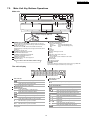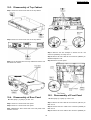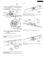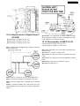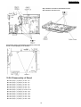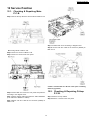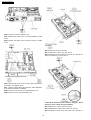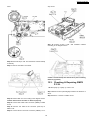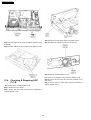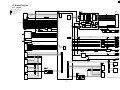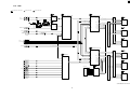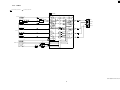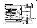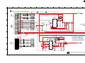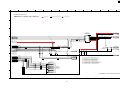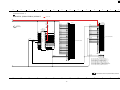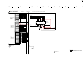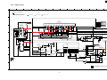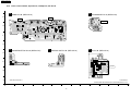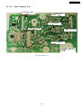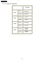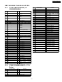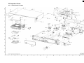
1
ORDER NO. MD0803025CE
A6
Blu-ray Disc Home Theater Sound System
SA-BT100P
SA-BT100PC
Colour
(K).......................Black Type
Specifications
250 W per channel (6 Ω), 1 kHz, 10% THD
Main unit SA-BT100P/PC
OGENERAL
Surround Ch:
Power supply:
125 W per channel (3 Ω), 1 kHz, 10% THD
AC 120 V, 60 Hz
iPod connector:
DC OUT 5V 500 mA MAX
Power consumption:
Center Ch:
250 W per channel (6 Ω), 1 kHz, 10% THD
This unit 140 W
Power consumption in standby mode:
Subwoofer Ch:
250 W per channel (6 Ω), 100 Hz, 10 % THD
approx. 0.3 W
Dimensions (W×H×D):
Total RMS TTL power:
With transmitter:
1250 W
430 mmx96 mmx327 mm
(16-15/16” X 3-25/32” X 12-7/8”)
FTC TTL Output Power:
Front Ch:
104 W per channel (6 Ω), 120Hz to 20 kHz, 1.0% THD
Without transmitter:
430 mmx90 mmx327 mm
Surround Ch:
34 W per channel (3 Ω), 120Hz to 20 kHz, 1.0% THD
(16-15/16” X 3-9/16” X 12-7/8”)
Mass:
Operating temperature range:
This unit approx 4.1 kg(9.1 lbs)
101 W per channel (6 Ω), 120Hz to 20 kHz, 1.0% THD
+0 °C to +40 °C
(+32 °F to +104 °F)
Operating humidity range:
Center Ch:
Subwoofer Ch:
95 W per channel (6 Ω), 45 Hz to120 Hz, 1.0% THD
35 % to 80 % RH
(no condensation)
Total FTC TTL power:
OAMPLIFIER SECTION
RMS TTL Output Power:
472 W
Audio Input:
Front Ch:
© 2008 Matsushita Electric Industrial Co. Ltd.. All
rights reserved. Unauthorized copying and
distribution is a violation of law.
SA-BT100P / SA-BT100PC
AUX:
*6
The total combined maximum number of recognizable picture
contents and folders: 9999 picture contents and 300 folders.
*7
AVCHD format V1.0
x1
Digital Audio Input:
OVIDEO SECTION
Optical:
Signal system:
x1
NTSC
Video output
OFM TUNER SECTION
1.0 Vp-p (75 Ω)
Output level:
Frequency Range:
87.9-107.9 MHz (200-kHz step)
Output connector:
87.5-108.0 MHz (100-kHz step)
Component Video Output
(1080i/720p/480p/480i)
OY output level:
1.0 Vp-p (75 Ω)
OPB output level:
0.7 Vp-p (75 Ω)
OPR output level:
0.7 Vp-p (75 Ω)
Antenna terminals
75 Ω (unbalanced)
ODISC SECTION
Pin jack (1 system)
Output connector Pin jack (Y: green, PB: blue, PR: red) (1
system)
Discs played:
(1) BD-Video:
HDMI AV output
BD-ROM Version 2
Output format:
(2) BD-RE:
480p (525p)/1080i (1125i)/720p (750p)/1080p (1125p)
Version 3 (Single Layer, Dual Layer), JPEG*6
Output connector:
(3) BD-R:
Type A (19 pin)
Version 2 (Single Layer, Dual Layer)
HDMITM (Deep color)
(4) DVD-RAM:
O
DVD Video Recording format, AVCHD format*7, JPEG*4
This unit supports “HDAVI Control 3” function.
Note:
(5) DVD-R/DVD-RW/DVD-R DL:
1. Specifications are subject to change without notice.
DVD-Video format*1,DVD-Video Recording format, AVCHD
format*1,7
Mass and dimensions are approximate.
2. Total harmonic distortion is measured by the digital spectrum
analyzer.
(6) +R/+RW/+R DL:
Video*1, AVCHD format*1,7
Solder:
(7) DVD-Video
This model uses lead free solder (PbF).
DVD-Video format
Mechanism:
(8) CD-Audio
This model uses BD/DVD Drive (VXY2001 SERIES)
CD-DA
Wireless Features:
(8) CD-R/RW
This Model supports wireless surround (e.g:SH-FX67)
CD-DA, JPEG*5, MP3
Optical pick-up
System with 2 lenses
Wavelength:
782 nm (CDs)/662nm
(DVDs)/405nm (BDs)
LaserSpecification
Class 1 LASER Product
Wavelength:
782 nm (CDs)/662 nm
(DVDs)/405 nm (BDs)
Laser power:
No hazardous radiation is
emitted with the safety
protection
SD CARD SECTION
Refer to their respective original service manuals for *1.
SD card slot:
Output connector (1 system)
SD card:
SD Memory Card*2 formatted
FAT12, FAT32*3. JPEG*4,
AVCHD format*7
*1
Finalizing is necessary.
*2
includes SDHC card
includes miniSD cards (need a miniSD Adaptor)
includes microSD cards (need a microSD Adaptor)
*3
Does not support long file name
*4
The total combined maximum number of recognizable picture
contents and folders: 3000 picture contents and 300 folders.
*5
The total combined maximum number of recognizable picture
contents and folders: 999 picture contents and 99 folders.
2
SA-BT100P / SA-BT100PC
CONTENTS
Page
1 Safety Precautions
Page
6
1.3. Protection Circuitry
7
1.1. GENERAL GUIDELINES
6
1.4. Safety Parts Information
7
1.2. Before Repair and Adjustment
6
3
SA-BT100P / SA-BT100PC
2 Prevention of Electrostatic Discharge (ESD) to
Electrostatically Sensitive (ES) Devices
9
3 Precaution of Laser Diode
10
4 About Lead Free Solder (PbF)
11
4.1. Service caution based on legal restrictions
5 Service Navigation
5.1. Service Information
12.3. Checking & Repairing SMPS P.C.B.
63
12.4. Checking & Repairing DSP P.C.B.
64
12.5. Checking & Repairing Digital P.C.B.
65
13 Caution for Replacing Parts
68
11
13.1. Notice after replacing Digital P.C.B.
68
12
13.2. Items that should be done after replacing parts
68
12
6 Accessories
13
7 Operation Procedures
13.3. Standard Inspection Specifications after Making Repairs 68
14 Voltage and Waveform Chart
69
14
14.1. DSP P.C.B. (IC3001 ~ IC3004)
69
7.1. Remote Control Key Buttons Operations
14
14.2. DSP P.C.B. (IC3101 ~ IC3104)
70
7.2. Main Unit Key Buttons Operations
15
14.3. DSP P.C.B. (IC3201 ~ QR3601)
71
7.3. Using the VIERA Link “HDAVI Control™”
16
14.4. D-Amp P.C.B.
72
7.4. Using the iPod
17
14.5. Main P.C.B. (IC100 ~ IC509)
73
7.5. Playing Secondary Video and Audio
19
14.6. Main P.C.B. (IC801 ~ QR7001)
74
7.6. Basic Connections
20
14.7. Panel P.C.B. (IC6001 ~ Q6003)
75
7.7. Disc and SD Cards Information
23
14.8. SMPS P.C.B. (IC5701 ~ QR5801)
75
14.9. Waveform Chart
76
8 Operation Instructions
26
15 Illustration of IC’s, Transistors and Diodes
78
26
16 Wiring Connection Diagram
79
27
17 Block Diagram
81
8.1. Taking out the Disc from BD/DVD Drive Unit when Disc
cannot be ejected by OPEN/CLOSE button
9 Service Mode
9.1. Self-Diagnosis and Special Mode Setting
27
17.1. Digital
81
9.2. Special Mode Setting
30
17.2. IC Terminal (Digital) Chart
82
9.3. Service Mode at glance
32
17.3. Digital P.C.B. Regulator
84
9.4. Service Mode Table (Wireless - e.g. SH-FX67)
37
17.4. DSP
85
39
17.5. IC Terminal (DSP) Chart
86
10.1. Disassembly Flow Chart
41
17.6. System Control
88
10.2. Main Components and P.C.B. Locations
42
17.7. Video
89
10.3. Disassembly of Top Cabinet
43
17.8. Audio Selector
90
10.4. Disassembly of Rear Panel
43
17.9. Audio
91
10.5. Disassembly of Front Panel
43
17.10. Digital Audio Amp
92
10.6. Disassembly of BD/DVD Drive Unit
44
17.11. Power
93
10 Assembling and Disassembling
18 Schematic Diagram Notes
95
45
19 Schematic Diagram
97
10.8. Disassembly of SD P.C.B.
46
19.1. Digital Circuit
10.9. Disassembly of Lid
46
19.2. DSP Circuit
113
10.10. Disassembly of Ipod Cradle P.C.B.
47
19.3. Main Circuit
119
10.11. Disassembly of AC Inlet P.C.B.
48
19.4. Panel, Power Button, Open/Close Circuit
125
10.12. Disassembly of Main P.C.B.
49
19.5. Headphone, SD, Wireless Adapter, Ipod Cradle Circuit 126
10.13. Disassembly of D-Amp P.C.B.
50
19.6. D-Amp Circuit
127
10.14. Replacement of Digital Amp IC (IC5000)
51
19.7. SMPS Circuit
129
10.15. Disassembly of SMPS P.C.B.
51
19.8. AC Inlet Circuit
131
10.16. Replacement of Switch Regulator IC (IC5701)
52
20 Printed Circuit Board
133
10.17. Replacement of Switch Regulator Diode (D5702)
53
20.1. Digital P.C.B.
133
10.18. Replacement of Regulator Diode (D5801)
54
20.2. DSP P.C.B.
134
10.19. Replacement of Regulator Diode (D5802)
55
20.3. Main P.C.B.
135
10.20. Replacement of Regulator Diode (D5803)
56
20.4. Panel, Power Button, Open/Close, Headphone, SD P.C.B.
10.21. Disassembly of Wireless Adapter P.C.B.
57
10.22. Disassembly of DSP P.C.B.
57
20.5. Wireless Adapter, Ipod Cradle, AC Inlet P.C.B.
137
10.23. Disassembly of Digital P.C.B.
58
20.6. D-Amp P.C.B.
138
10.24. Disassembly of Stand
59
20.7. SMPS P.C.B.
139
10.7. Disassembly of Panel/ Headphone/ Power / Open/close
P.C.B.
11 Service Fixture and Tools
60
12 Service Position
61
12.1. Checking & Repairing Main P.C.B.
61
12.2. Checking & Repairing D-Amp P.C.B.
61
97
136
21 Basic Troubleshooting Guide
21.1. Troubleshooting Guide for F61 and/or F76
22 Terminal Function of ICs
22.1. IC1103 (MFI341S2095): IC COPROCESSOR
4
141
141
147
147
SA-BT100P / SA-BT100PC
22.2. IC6001(C0HBB0000057): IC FL Driver
23 Exploded Views
24 Replacement Parts List
147
149
23.1. Cabinet Parts Location
149
23.2. Packaging
151
24.1. Component Parts List
25 Schematic Diagram for printing with letter size
5
153
154
175
SA-BT100P / SA-BT100PC
1 Safety Precautions
1.1.
GENERAL GUIDELINES
1. When servicing, observe the original lead dress. If a short circuit is found, replace all parts which have been overheated or
damaged by the short circuit.
2. After servicing, see to it that all the protective devices such as insulation barriers, insulation papers shields are properly
installed.
3. After servicing, carry out the following leakage current checks to prevent the customer from being exposed to shock hazards.
1.1.1.
LEAKAGE CURRENT COLD CHECK
1. Unplug the AC cord and connect a jumper between the two prongs on the plug.
2. Measure the resistance value, with an ohmmeter, between the jumpered AC plug and each exposed metallic cabinet part on
the equipment such as screwheads, connectors, control shafts, etc. When the exposed metallic part has a return path to the
chassis, the reading should be between 1MΩ and 5.2MΩ.
When the exposed metal does not have a return path to the chassis, the reading must be
1.1.2.
LEAKAGE CURRENT HOT CHECK
1. Plug the AC cord directly into the AC outlet. Do not use an isolation transformer for this check.
2. Connect a 1.5kΩ, 10 watts resistor, in parallel with a 0.15µF capacitors, between each exposed metallic part on the set and a
good earth ground such as a water pipe, as shown in Figure 1.
3. Use an AC voltmeter, with 1000 ohms/volt or more sensitivity, to measure the potential across the resistor.
4. Check each exposed metallic part, and measure the voltage at each point.
5. Reverse the AC plug in the AC outlet and repeat each of the above measurements.
6. The potential at any point should not exceed 0.75 volts RMS. A leakage current tester (Simpson Model 229 or equivalent) may
be used to make the hot checks, leakage current must not exceed 1/2 milliamp. In case a measurement is outside of the limits
specified, there is a possibility of a shock hazard, and the equipment should be repaired and rechecked before it is returned to
the customer.
Figure 1
1.2.
Before Repair and Adjustment
Disconnect AC power to discharge unit AC Capacitors as such C5700, C5701, C5702, C5703, C5704 through a 10 Ω, 10 W
resistor to ground.
Caution:
DO NOT SHORT-CIRCUIT DIRECTLY (with a screwdriver blade, for instance), as this may destroy solid state devices.
After repairs are completed, restore power gradually using a variac, to avoid overcurrent.
Current consumption at AC 120 V, 60 Hz in NO SIGNAL mode volume minimal should be ~ 900 mA.
6
SA-BT100P / SA-BT100PC
1.2.1.
1.3.
Caution for fuse replacement
Protection Circuitry
The protection circuitry may have operated if either of the following conditions are noticed:
• No sound is heard when the power is turned on.
• Sound stops during a performance.
The function of this circuitry is to prevent circuitry damage if, for example, the positive and negative speaker connection wires are
“shorted”, or if speaker systems with an impedance less than the indicated rated impedance of the amplifier are used.
If this occurs, follow the procedure outlines below:
1. Turn off the power.
2. Determine the cause of the problem and correct it.
3. Turn on the power once again after one minute.
Note:
When the protection circuitry functions, the unit will not operate unless the power is first turned off and then on again.
1.4.
Safety Parts Information
Safety Parts List:
There are special components used in this equipment which are important for safety.
These parts are marked by
in the Schematic Diagrams & Replacement Parts List. It is essential that these critical parts
should be replaced with manufacturer’s specified parts to prevent shock, fire or other hazards. Do not modify the original design
without permission of manufacturer.
Table 1
Ref. No.
1
5
6
28
33
33
38
A2
PCB2
PCB3
PCB11
PCB12
IC103
IC3002
IC3102
IC51001
IC51302
IC51303
DZ5701
L5701
L5702
L5703
T5701
T5751
T7001
PC5701
Part No.
J0KD00000126
REXX0640-J
REXX0641-J
VXY2001-SER
RGR0382A-A2
RGR0382A-B2
RKM0592-K
K2CB2CB00021
RFKB4368A
RFKB4370A
REPX0622V
REPX0622V
RFKWEDF001PA
RFKWBT100DS1
RFKWBT100DS2
MN2WS0043AP
C3FBSC000029
C3ZBL0000027
ERZV10V511CS
ELF15N035AN
ELF22V035B
ELF22V035B
ETS42BM19GAC
ETS19AB281AG
G4D1A0000117
B3PBA0000402
Part Name & Description
FERRITE CORE
BLACK WIRE (AC-SMPS)
RED WIRE (AC-SMPS)
BD DRIVE UNIT
REAR PANEL
REAR PANEL
TOP CABINET
AC CORD
DIGITAL PCB
MAIN PCB
SMPS PCB
AC INLET P.C.B
IC EEPROM
IC FLASH ROM
IC FLASH ROM
IC DV LSI
IC NAND FLASH ROM
IC EEPROM
ZENER
LINE FILTER
LINE FILTER
LINE FILTER
MAIN TRANSFORMER
BACKUP TRANSFORMER
SWITCHING TRANSFORMER
PHOTO COUPLER
7
Remarks
[M]
[M]
[M]
[M]
[M]
[M]
[M]
[M]
[M]
[M]
[M]
[M]
[M]
[M]
[M]
[M]
[M]
[M]
[M]
[M]
[M]
[M]
[M]
[M]
[M]
[M]
P
PC
(RTL)
(RTL)
(RTL)
(RTL)
(RTL)
SA-BT100P / SA-BT100PC
Ref. No.
PC5702
PC5720
PC5799
F1
IP7001
IP58301
TH5701
TH5860
P5701
C5700
C5701
C5702
C5703
C5704
Part No.
B3PBA0000402
B3PBA0000402
B3PBA0000402
K5D802APA008
K5H7512A0010
ERBSE3R00U
D4CAA2R20001
D4CC11040013
K2AB2B000010
F1BAF1020020
ECQU2A104MLC
ECQU2A104MLC
ECQU2A104MLC
F1BAF1020020
Part Name & Description
PHOTO COUPLER
PHOTO COUPLER
PHOTO COUPLER
FUSE
PROTECTOR
PROTECTOR
THERMISTOR
THERMISTOR
AC INLET
1000pF
0.1uF
0.1uF
0.1uF
1000pF
8
Remarks
[M]
[M]
[M]
[M]
[M]
[M]
[M]
[M]
[M]
[M]
[M]
[M]
[M]
[M]
SA-BT100P / SA-BT100PC
2 Prevention of Electrostatic Discharge (ESD) to
Electrostatically Sensitive (ES) Devices
Some semiconductor (solid state) devices can be damaged easily by static electricity. Such components commonly are called
Electrostatically Sensitive (ES) Devices. Examples of typical ES devices are integrated circuits and some field-effect transistors and
semiconductor "chip" components. The following techniques should be used to help reduce the incidence of component damage
caused by electrostatic discharge (ESD).
1. Immediately before handling any semiconductor component or semiconductor-equipped assembly, drain off any ESD on your
body by touching a known earth ground. Alternatively, obtain and wear a commercially available discharging ESD wrist strap,
which should be removed for potential shock reasons prior to applying power to the unit under test.
2. After removing an electrical assembly equipped with ES devices, place the assembly on a conductive surface such as
aluminum foil, to prevent electrostatic charge buildup or exposure of the assembly.
3. Use only a grounded-tip soldering iron to solder or unsolder ES devices.
4. Use only an anti-static solder removal device. Some solder removal devices not classified as "anti-static (ESD protected)" can
generate electrical charge sufficient to damage ES devices.
5. Do not use freon-propelled chemicals. These can generate electrical charges sufficient to damage ES devices.
6. Do not remove a replacement ES device from its protective package until immediately before you are ready to install it. (Most
replacement ES devices are packaged with leads electrically shorted together by conductive foam, aluminum foil or comparable
conductive material).
7. Immediately before removing the protective material from the leads of a replacement ES device, touch the protective material
to the chassis or circuit assembly into which the device will be installed.
Caution:
Be sure no power is applied to the chassis or circuit, and observe all other safety precautions.
8. Minimize bodily motions when handling unpackaged replacement ES devices. (Otherwise harmless motion such as the
brushing together of your clothes fabric or the lifting of your foot from a carpeted floor can generate static electricity (ESD)
sufficient to damage an ES device).
9
SA-BT100P / SA-BT100PC
3 Precaution of Laser Diode
CAUTION :
This product utilizes a laser diode with the unit turned "on", invisible laser radiation is emitted from the pickup lens.
Wavelength: 662 nm (DVD)/782 nm (CD)/405 nm (BD)
Maximum output radiation power from pickup: 100 µW/VDE
Laser radiation from the pickup unit is safety level, but be sure the followings:
1. Do not disassemble the pickup unit, since radiation from exposed laser diode is dangerous.
2. Do not adjust the variable resistor on the pickup unit. It was already adjusted.
3. Do not look at the focus lens using optical instruments.
4. Recommend not to look at pickup lens for a long time.
10
SA-BT100P / SA-BT100PC
4 About Lead Free Solder (PbF)
4.1.
Service caution based on legal restrictions
4.1.1.
General description about Lead Free Solder (PbF)
The lead free solder has been used in the mounting process of all electrical components on the printed circuit boards used for this
equipment in considering the globally environmental conservation.
The normal solder is the alloy of tin (Sn) and lead (Pb). On the other hand, the lead free solder is the alloy mainly consists of tin
(Sn), silver (Ag) and Copper (Cu), and the melting point of the lead free solder is higher approx.30 degrees C (86°F) more than that
of the normal solder.
Definition of PCB Lead Free Solder being used
The letter of “PbF” is printed either foil side or components side on the PCB using the lead free solder.
(See right figure)
Service caution for repair work using Lead Free Solder (PbF)
• The lead free solder has to be used when repairing the equipment for which the lead free solder is used.
(Definition: The letter of “PbF” is printed on the PCB using the lead free solder.)
• To put lead free solder, it should be well molten and mixed with the original lead free solder.
• Remove the remaining lead free solder on the PCB cleanly for soldering of the new IC.
• Since the melting point of the lead free solder is higher than that of the normal lead solder, it takes the longer time to melt
the lead free solder.
• Use the soldering iron (more than 70W) equipped with the temperature control after setting the temperature at 350±30
degrees C (662±86°F).
Recommended Lead Free Solder (Service Parts Route.)
• The following 3 types of lead free solder are available through the service parts route.
RFKZ03D01K-----------(0.3mm 100g Reel)
RFKZ06D01K-----------(0.6mm 100g Reel)
RFKZ10D01K-----------(1.0mm 100g Reel)
Note
* Ingredient: tin (Sn), 96.5%, silver (Ag) 3.0%, Copper (Cu) 0.5%, Cobalt (Co) / Germanium (Ge) 0.1 to 0.3%
11
SA-BT100P / SA-BT100PC
5 Service Navigation
5.1.
Service Information
The service manual contains technical information which will allow service personnel’s to understand
and service this model.
Please place orders using the parts list and not the drawing reference numbers.
If the circuit is changed or modified, the information will be followed by supplement service manual to be filed with
original service manual.
1) This service manual does not contain the following information, because of the impossibility of servicing at
component level.
* Schematic Diagram, Block Diagram and P.C.B. layout of Digital P.C.B..
* Parts List for individual parts of Digital P.C.B..
* Exploded View and Parts List for individual parts of BD/DVD drive.
2) The following category are recycle modeule part. Please send them to Central Repair Center.
* Digital P.C.B. (BT100P/PC : RFKB4368A)
3) For BD/DVD Drive, it depends on area to defferent recycle system.
Please refer to service policy in detail.
* BD/DVD drive (VXY2001-SER)
12
SA-BT100P / SA-BT100PC
6 Accessories
• Note: Refer to “Replacement Parts List” (Section 25) for the part number.
AM loop antenna
Remote control
AC cord
(For SA-BT100 & SH-FX67)
FM Indoor Antenna
Video cable
Speaker cable sticker
Speaker cables
13
SA-BT100P / SA-BT100PC
7 Operation Procedures
7.1.
Remote Control Key Buttons Operations
Remote control
14
15
1
1 Turn the unit on and off
2 Select the source
3
4
5
2
16
3
17
4
6
7
8
9
10
18
11
12
13
5
6
19
7
20
14
15
[BD/SD]: Select disc drive or SD card drive
[FM/AM]: Select FM/AM tuner
[iPod]:
Select iPod as the source
Numbered buttons
Select preset radio stations and title numbers, etc./Enter numbers
Cancel
Basic playback control buttons
[
,
]: Select preset radio stations
[ , ]:
Select radio station manually
Show on-screen menu
Show Pop-up menu
Show Top Menu/Direct Navigator
Show sub menu
These buttons are used when operating a BD-Video disc that
includes JavaTM applications (BD-J). For more information about
operating this kind if disc, please read the instructions that came
with the disc.
The [A] and [B] buttons are also used with the "Title View", "Picture
View" and "Album View" screens
Show Setup menu
Remove interference during radio reception
[SOUND]:
Set the sound effect
[SLEEP]:
Set the sleep timer
[CH SELECT]:
Select speaker channel
[MUTING]:
Mute the sound
Transmit the remote control signal
TV operation buttons
Aim the remote control at the Panasonic TV and press the button.
[ TV]:
Turn the TV on and off
[TV/VIDEO]: Switch the input channel
[ VOL]:
Adjust the TV volume
This may not work properly with some models.
Select the source
BD/DVD/CD
SD
FM
AM
IPOD
D-IN AUX
8
21
9
22
16
23
17 Adjust the volume of the main unit
18 Select audio
10
11
24
12
25
19 Start up and play a disc automatically
20 [
13
21
22
23
24
25
, , , ]:
Menu selection
[OK]:
Selection
[ , ]:
Select preset radio station
[ ] ( ),[ ] ( ):
Frame-by-frame
Show FUNCTIONS menu
Return to previous screen
[PIP]:Switch on/off Secondary Video (Picture-in-picture)
[SECONDARY AUDIO]:Switch on/off Secondary Audio
Show status messages
Enjoy surround sound
Wireless system
1
POWER
1 Unit on/off button [POWER
,
]
2 Use this button to turn the unit on and off.
2
: This unit is on.
: This unit is off.
AUTO OPERATION ON/OFF
AUTO OPERATION ON/OFF POWER indicator
The indicator lights red when the wireless system is turned on and
lights green when the wireless link is activated. When the wireless
link is inactive for a long time, it turns red.
14
SA-BT100P / SA-BT100PC
7.2.
Main Unit Key Buttons Operations
Main unit
1
2
3
4
11
5
6
SW
BOOST
7.1CH
D.S.P.
12
7
8
9
10
SELECTOR
13
14
15
18
Place your finger on the section
and open it diagonally downwards.
16
17
1
2
3
4
5
6
7
POWER button (POWER / )
Press to switch the unit form on to standby mode vice versa. In
standby mode, the unit is still consuming a small amount of power.
Standby/on indicator ( )
When the unit is connected to the household AC outlet, this
indicator lights up in standby mode and goes out when the unit is
turned on.
Open or close the disc tray
SW BOOST (Subwoofer boost) button
Turn Subwoofer boost on/off
SW BOOST (Subwoofer boost) indicator
Lights when Subwoofer boost is on
7.1CH D.S.P. indicator
Illuminated during 7.1ch source playback.
Select the source
BD/DVD/CD
SD
FM
AM
IPOD
D-IN AUX
Select the radio station manually
Search /Slow-motion/Skip
Search:
Press and hold (During play)
Slow-motion:
Press and hold (During pause)
Skip:
Press
9 Stop
10 Start play
11 Disc tray
12 Remote control signal sensor
13 Display
14 Adjust the volume of the main unit
15 Volume indicator
It is possible to set the indicator to turn on/off.
16 SD card slot
17 Connect iPod
18 Headphone terminal
Rear panel terminals
CAUTION
Do not place objects in front of the unit. The disc tray may collide with
objects when it is opened, and this may cause injury.
8
The unit’s display
1
2
3
DISC iPod SD SLP TUNED
MONO ST M DTS
D
PL x
W2S
W4S
4
1
iPod
SD
2
3
W4S
7
Main display section
iPod indicator
Illuminated during iPod repeat playback
Lights when iPod is ready to play.
Lights when SD card is ready to play.
Illuminated during iPod shuffle playback
7
Audio signal indicator
Lights when DTS decoder is being used.
DTS
DTS
DTS
DTS
Lights when set to monaural reception.
Lights when set to stereo broadcast reception.
Lights when DTS-HD decoder is being used.
Lights when DTS-ES decoder is being used.
96/24
D
Flashes during preset channel registration.
D
Wireless link indicator
W2S
6
5
6
The indicator blinks when reading data.
SLEEP indicator
Radio broadcast display
TUNED Lights when receiving a radio broadcast.
MONO
ST
M
4
5
Drive indicator
Lights when disc is ready to play.
DISC
96/24
D
HD
NEO:6
PL
Lights when speaker setting is set to 5.1ch and
link with wireless system is activated.
PL x
Lights when speaker setting is set to 7.1ch and
link with wireless system is activated.
HD
NEO:6
The indicator blinks when the wireless link is inactive for
a long time.
15
Lights when DTS 96/24 decoder is being used.
Lights when Dolby Digital decoder is being used.
Lights when Dolby Digital Plus decoder is
being used.
Lights when Dolby Pro Logic II decoder is
being used.
Lights when Dolby Pro Logic IIx decoder is
being used.
Lights when Dolby TrueHD decoder is
being used.
Lights when DTS NEO:6 matrix decoder is
being used.
SA-BT100P / SA-BT100PC
7.3.
Using the VIERA Link “HDAVI Control™”
(VIERA LinkTM H DAVI ControlTM )
What is VIERA Link HDAVI Control ?
VIERA LinkTM is a new name for EZ SyncTM.
VIERA Link HDAVI Control is a convenient function that offers linked
operations of this unit, and a Panasonic TV (VIERA) under HDAVI
Control . You can use this function by connecting the equipment with an
HDMI cable. See the operating instructions for connected equipment for
operational details.
Preparation
1
2
3
Confirm that the HDMI connection has been made
Set VIERA Link to On
To complete and activate the connection correctly, turn on all VIERA Link
HDAVI Control compatible equipment and set the TV to the corresponding
HDMI input mode for this unit.
Setting the TV audio for VIERA Link HD AVI Control
Select between AUX and D-IN to work with the linked operations. Confirm
the audio connection to the AUX terminal (for AUX ) or OPTICAL IN terminal
(for D-IN )
1
2
3
4
5
Press [ , SELECT] to select AUX or D-IN .
Press [SETUP].
(When D-IN is selected)
Press [ , ] to select TV SOUND .
Press [OK].
Press [ , ] to switch AUX or D-IN and press [OK].
NOTE
VIERA Link HDAVI Control , based on the control
functions provided by HDMI which is an industry
standard known as HDMI CEC (Consumer
Electronics Control), is a unique function that we
have developed and added. As such, its operation
with other manufacturers equipment that supports
HDMI CEC cannot be guaranteed.
This unit supports HDAVI Control 3 function.
HDAVI Control 3 is the newest standard (current as
of December, 2007) for Panasonic s HDAVI Control
compatible equipment. This standard is compatible
with Panasonic s conventional HDAVI equipment.
Please refer to individual manuals for other
manufacturers equipment supporting VIERA Link
function.
It is recommended that you use Panasonic s
HDMI cable.
Recommended p art num ber:
RP-CDHG10 (1.0 m/3.3 ft.), RP-CDHG15 (1.5 m/
4.9 ft.),RP-CDHG20 (2.0 m/6.6 ft.), RP-CDHG30
(3.0 m/9.8 ft.), RP-CDHG50 (5.0 m/16.4 ft.), etc.
Non-HDMI-compliant cables cannot be utilized.
Whenever the connection or settings are changed, reconfirm the points above.
What you can do with HDAVI Control
One touch play
Speaker control
You can turn on this unit and TV, and start playing with a single press
of a button.
You can select whether audio is output from the unit s speakers or the
TV speakers by using the TV menu settings. For details, refer to the
operating instructions of your TV.
Press [ONE TOUCH PLAY].
This unit s speakers will be automatically activated (
control).
Home theater
This unit s speakers are active.
When this unit is in standby mode, changing the TV speakers to this
unit s speakers in the TV menu will automatically turn the unit on and
select AUX * or D-IN * as the source.
The TV speakers are automatically muted.
You can control the volume setting using the volume or mute button
on the TV s remote control. (The volume level is displayed on the
main unit s FL display.)
To cancel muting, you can also use the home theater remote control
If you turn off this unit, TV speakers will be automatically activated.
right, Speaker
This function also works if you press [ ] (PLAY) on this unit s
remote control when this unit is in standby mode.
Playback may not be immediately displayed on the TV. If you miss
the beginning portion of playback, press [
] or [
] to go back to
where playback started.
Automatic input switching
When you switch the TV input to TV tuner mode, this unit will
automatically switch to AUX * or D-IN * .
[This function does not work when the iPod selector (SIMPLE mode)
is chosen.]
When you start disc play, the TV will automatically switch its input
mode for this unit.
TV
TV speakers are active.
The volume of this unit is set to 0 .
This function works only when BD/DVD/CD , SD , AUX * or
D-IN * is selected as the source on the home theater system.
Audio output is 2-channel audio.
Automatic lip-sync function (for HDAVI Control 3)
Delay between audio and video is automatically adjusted, enabling
you to enjoy smooth audio for the picture
This function works only when BD/DVD , SD , AUX * or D-IN * is
selected as the source on this unit.
*
AUX or D-IN works depending on the TV SOUND setting (
Power off link
When the TV is turned off, this unit goes into standby mode
automatically.
This function works only when BD/DVD/CD , SD , IPOD , AUX *
or D-IN * is selected as the source on this unit.
above, Setting the TV audio for VIERA Link HDAVI Control ).
16
SA-BT100P / SA-BT100PC
7.4.
Using the iPod
Preparation
To view videos/photos from the iPod.
Ensure the video connection to the VIDEO OUT terminal on this unit.
Operate the iPod menu to make the appropriate video/photo output settings for your TV.
To display the picture, turn on the TV and select the appropriate video input mode.
Before connecting/disconnecting the iPod, turn the main unit off or reduce the volume of the main unit to its minimum.
1
Open the Dock for iPod.
About dock adapter
Place your finger on the section
and open it diagonally downwards.
NOTE
Dock for iPod
About recharging the battery
iPod will start recharging regardless of whether this
unit is on or off.
IPOD
will be shown on the main unit s display
during iPod charging in main unit standby mode.
Check iPod to see if the battery is fully recharged.
If you are not using iPod for an extended period of
time after recharging has completed, disconnect it
from main unit, as the battery will be depleted
naturally. (Once fully recharged, additional
recharging will not occur.)
Main unit
2
Attach the dock adapter which should be supplied
with your iPod to the dock for the stable use of the
iPod. If you need an adapter, consult your iPod
dealer.
Connect the iPod (not included) firmly.
Recharging starts when the iPod is inserted.
e.g.,
iPod
Dock adapter
(not included)
Main unit
Hold the dock when connecting/
disconnecting the iPod.
Compatible iPod
Name
Memory size
iPod touch
8 GB, 16 GB
iPod nano 3rd generation (video)
4 GB, 8 GB
iPod classic
80 GB, 160 GB
iPod nano 2nd generation (aluminum)
2 GB, 4 GB, 8 GB
iPod 5th generation (video)
60 GB, 80 GB
iPod 5th generation (video)
30 GB
iPod nano 1st generation
1 GB, 2 GB, 4 GB
iPod 4th generation (color display)
40 GB, 60 GB
iPod 4th generation (color display)
20 GB, 30 GB
iPod 4th generation
40 GB
iPod 4th generation
20 GB
iPod mini
4 GB, 6 GB
NOTE
Compatibility depends on the software version of
your iPod.
Audio/video cannot be recorded or transmitted to
iPods via this system.
Panasonic makes no warranty over iPod data
management.
For more information, refer to the operating
instructions for iPod.
The contents of the operating instructions and
those displayed on iPod may differ partially, but this
will not fundamentally affect use of music
playback.
17
SA-BT100P / SA-BT100PC
Playback
This system features two different iPod playback modes.
The first of these is EXTENDED mode, for playback of music contents. With this mode, the menu screen on the system can be used to search for
playlists and artist names, and to play music. The second mode is SIMPLE mode, which can be used for playback of three types of contents
music, photos, and videos. With this mode, simple operations such as play, stop, and search can be performed on the display of your iPod.
Enjoy music (EXTENDED mode)
Enjoy videos/photos (SIMPLE mode)
1 Press [iPod] to select IPOD .
You can also play music using SIMPLE mode.
The iPod automatically switches to this unit s display mode.
iPod Music menu appears on the TV.
If the menu screen is not displayed, press [SETUP].
1 Press [iPod] to select IPOD .
2 Press [SETUP] to switch the iPod to its own
display mode.
iPod Music
Proceed operations through display of iPod.
If the iPod Music menu ( left) is displayed, press [SETUP].
SIMPLE will be shown on the main unit s display.
Playlists
Ar tists
Alb ums
Son gs
3 Switch the TV input to video in.
Podcasts
Audiobooks
Playbac k Mode
4 Play a slideshow or video on your iPod.
OK
Items
The picture will be displayed on your TV.
Artists
Selection/playback method
Search from all playlists.
Search by artist name.
Albums
Search by album title.
Songs
Search from all songs registered on iPod.
Playlists
You can also use the remote control to operate iPod menu.
[ , ]:
To navigate menu items
[OK]:
To go to the next menu
[RETURN]: To return to the previous menu
Search by episode for radio programs
downloaded from iTunes store.
Podcasts
Audiobooks Search by title from audiobooks purchased from
iTunes store or audible.com.
Shuffl
e
Playback
Off:
Cancel
Mode*
Songs: Play all songs on iPod in random order.
Albums: Play all songs on album in random
order.
is displayed on the unit s display when
Basic controls (For music and videos only)
Buttons
[ ] (PLAY)
,
] to select an item and press [OK].
e.g.,
Playing condition
iPod
Good morning
Ronaldo
Happy days
2:43
Playing
position
]
Skip
Search
You can enjoy surround sound effect when you press [
[NEO:6]
Play will start from the selected song if this operation is
repeated several times.
Press [RETURN] to return to the previous screen.
Song
Artist
Album
,
(Press and hold)
[
,
]
Playback modes during connection/when disconnected
System may be operated in same playback mode as set with
iPod when connected. Playback may also be continued on iPod
with same settings as made on system after disconnection.
2 Press [
Press [ ] (PLAY) to restart play.
Playback start position may not be
stored in memory in certain cases.
[ ]
[
Play
Pause
[ ]
Songs or Albums is selected.
Repeat
Off:
Cancel
One:
Play single song repeatedly.
All:
Play all songs from selected item (e.g.,
Playlists, Albums, etc.) repeatedly.
is displayed on the unit s display when
One or All is selected.
*
Functions
45 of 1230
Pause Play
Skip
RETURN
Skip
Clear/display iPod Music menu during playback.
Press [TOP MENU].
18
PLIIx] or
SA-BT100P / SA-BT100PC
7.5.
Playing Secondary Video and Audio
Playing secondary video (picture-in-picture) and secondary audio
Secondary video can be played from a disc compatible with the picture-in-picture
function.
For the playback method, refer to the instructions for the disc.
Secondary video
To turn on/off secondary video
Press [PIP].
Secondary video is played.
PiP ON is displayed.
Press the button to turn it ON and OFF.
To turn on/off audio with the secondary video
Press [SECONDARY AUDIO].
Primary video
The secondary audio is played.
Secondary Audio ON is displayed.
Press the button to turn it ON and OFF.
19
Only the primary video is played during search/
slow-motion or frame-by-frame.
NOTE
SA-BT100P / SA-BT100PC
7.6.
Basic Connections
7.6.1.
Speaker Cables and Transmitter Connection
Do not place the unit on amplifiers or equipment that may become hot. The heat can damage the unit.
Turn off all equipment before connection and read the appropriate operating instructions.
Speaker cables and transmitter connection
Sheet of speaker cable
stickers
Speaker cable for front
speaker (L) (White)
Speaker cable for front
speaker (R) (Red)
Speaker cable for surround
speaker (R) (Grey)
Speaker cable for center
speaker (Green)
Digital transmitter
Speaker cable for surround
speaker (L) (Blue)
Preparation
Attach the speaker cable stickers to make connection
easier.
Set the surround selector at the rear of the wireless
system to tis center.
e.g., Center speaker
SURR
SURR
SURR
SPEAKERS
NCEINTES
LS / RB LB / RS
AC IN
I/D SET
SURR
CENTER
5
Do
CENTER
Speaker cable sticker
(included)
5
Do not
SURROU ND (3 6 )
L
R
SIDE SIDE AMBIOPHONIQUES
Do not
Digital transmitter
Insert fully until you
hear a click.
Main unit
SURROU ND
SURROU ND
BACK
OPTICAL IN VIDEO OUT
PR
AUX
Wireless system
AM ANT
EXT
OUT
L
SPEAKERS
SPEAKERS
ENCEINTES
LS / RB LB / RS
LOOP
DIGITAL
Y
PB
COMPONENT VIDEO OUT
R
DIGITAL
TRANSMITTER
LOOP
ANT
GND
AC IN
FM ANT
75
I/D SET
SURR
AC IN
2
6
5
6
6
R 6
SUBWOOFER CENTER
Purple Green
1
L FRO NT
Red
SURROU ND (3 6 )
L
R
SIDE SIDE AMBIOPHONIQUES
AV OUT
White
Blue
Grey
Connect to the terminals of the
same color.
Subwoofer
Speaker cable (included)
Front speaker (R)
Front
Front speaker (L)
Surround
speaker (L)
Surround
speaker (R)
Front
Surround
Surround
Center speaker
Center
NOTE
Do not use a front speaker as a surround speaker or vice versa. Verify the type of speaker with the label on the rear of the
speaker.
Do not insert or remove the digital transmitter while the main unit is on.
Insert the wires fully.
: White
: Blue
Push!
Be careful not to cross (short-circuit) or reverse the polarity of the speaker wires as doing so may damage the speakers.
Do not
20
SA-BT100P / SA-BT100PC
7.6.2.
Connecting to a Television with HDMI & Video Cable
Connection to a TV
Do not connect through the video cassette recorder. Due to copy guard protection, the picture may not display properly.
With an HDMI cable
HDMI
compatible
TV
OPTICAL
OUT
AUDIO OUT
AV IN
L
R
Main unit
HDMI cable (not included)
SURROU ND
SURROU ND
BACK
OPTICAL IN VIDEO OUT
PR
AUX
AM ANT
EXT
OUT
L
SPEAKERS
LOOP
PB
R
COMPONENT VIDEO OUT
AC IN
2
6
5
6
6
R 6
SUBWOOFER CENTER
Optical
digital audio
cable *
(not included)
OPTICAL IN VIDEO OUT
PR
AUX
AM ANT
EXT
L
LOOP
LOOP
ANT
GND
DIGITAL
Y
Audio cable *
(not included)
The optical digital
audio cable can be
used when connecting
to televisions with
optical out terminals
( right).
LOOP
ANT
GND
DIGITAL
Y
PB
R
COMPONENT VIDEO OUT
FM ANT
75
FM ANT
75
1
1
L FRO NT
L FRO NT
AV OUT
AV OUT
Please use High Speed HDMI cables that have the HDMI logo (as shown on the cover).
It is recommended that you use Panasonic’s HDMI cable.
Recommended part number:
NOTE RP-CDHG10 (1.0 m/3.3 ft.), RP-CDHG15 (1.5 m/4.9 ft.), RP-CDHG20 (2.0 m/6.6 ft.),
RP-CDHG30 (3.0 m/9.8 ft.), PR-CDHG50 (5.0 m/16.4 ft.), etc.
NECESSARY SETTINGS
"HDMI Video Mode" : "On"/"HDMI Audio Output" : "Off"
With this connection, you can use VIERA Link "HDAVI Control"
* These audio connections will enable you to play audio from your television through your home theater system
With Video cable
Video cable
VIDEO IN
OPTICAL
OUT
TV
AUDIO IN
AUDIO OUT
L
L
R
R
Video cable (included)
Main unit
SURROU ND
SURROU ND
BACK
OPTICAL IN VIDEO OUT
PR
AUX
AM ANT
EXT
OUT
L
SPEAKERS
LOOP
DIGITAL
Y
PB
COMPONENT VIDEO OUT
AC IN
2
6
5
6
6
R 6
SUBWOOFER CENTER
R
LOOP
ANT
GND
OPTICAL IN VIDEO OUT
PR
AUX
AM ANT
EXT
L
LOOP
DIGITAL
Y
PB
COMPONENT VIDEO OUT
FM ANT
75
R
LOOP
ANT
GND
FM ANT
75
1
1
L FRO NT
Optical
digital audio
cable *
(not included)
Audio cable *
(not included)
The optical digital
audio cable can be
used when connecting
to televisions with
optical out terminals
( right).
L FRO NT
AV OUT
AV OUT
Optional connections
For those who want to enjoy higher picture quality and have a TV equipped with an HDMI terminal
For those who want to enjoy higher picture quality and have a TV equipped with a COMPONENT VIDEO IN terminal
NOTE For those who have a Set Top Box (Satellite receiver, Cable box, etc) or video cassette recorder
*These audio connections will enable you to play audio from your television through your home theater system
21
SA-BT100P / SA-BT100PC
7.6.3.
Radio Antenna and AC Power Supply Cord Connections
Radio antenna connections
FM Indoor antenna
AM loop antenna
AM loop antenna (included)
Stand the antenna up on its base.
Place the antenna where reception
is best.
Red
White
FM indoor antenna (included)
Affix this end of the antenna where
reception is best.
Adhesive tape
Main unit
SURROU ND
SURROU ND
BACK
OPTICAL IN VIDEO OUT
PR
AUX
Click!
AM ANT
EXT
OUT
L
SPEAKERS
LOOP
DIGITAL
Y
PB
R
COMPONENT VIDEO OUT
DIGITAL
TRANSMITTER
LOOP
ANT
GND
FM ANT
75
Black
AC IN
2
6
5
6
6
R 6
SUBWOOFER CENTER
1
L FRO NT
AV OUT
1
2
Push!
3
Keep loose antenna cables away from other wires and cables.
NOTE
Optional connections
Using FM/AM outdoor antenna (optional)
AC power supply cord connections
AC power supply cord
Wireless system
Main unit
SURROU ND
SURROU ND
BACK
OPTICAL IN VIDEO OUT
PR
AUX
AM ANT
EXT
OUT
SPEAKERS
ENCEINTES
LS / RB LB / RS
L
SPEAKERS
LOOP
DIGITAL
Y
PB
COMPONENT VIDEO OUT
R
DIGITAL
TRANSMITTER
LOOP
ANT
GND
ACI N
FM ANT
75
SURR
AC IN
2
6
5
6
6
R 6
SUBWOOFER CENTER
SURROU ND (3 6 )
L
R
SIDE SIDE AMBIOPHONIQUES
1
L FRO NT
I/D SET
AV OUT
AC power supply cord
(included)
AC power supply cord
(included)
To a househeld AC outlet
(AC 120V, 60Hz)
To a househeld AC outlet
(AC 120V, 60Hz)
Power consumption
The main unit and the wireless system consume a small amount of power when they are turned off (Main unit: approx. 0.3 W, wireless
system: approx. 0.2 W). To save power when they are not to be used for a long time, unplug them from the household AC outlet.
NOTE You will need to reset some memory items after plugging in the main unit.
The included AC power supply cords are for use with the main unit and wireless system only. Do not use them with other equipment.
Also, do not use cords for other equipment with the main unit or wireless system.
When the AC power supply cord is connected for the first time, "PLEASE WAIT" is displayed on the main unit’s display for about
30 seconds and power is turned off automatically.
22
SA-BT100P / SA-BT100PC
7.6.4.
Setting up the unit
Turn on the main unit and wireless system
Turn on the power of the main unit and the wireless system after all connections are complete.
AUTO OPERATION ON/OFF
indicator
1
Preparation
Turn on the TV and select the appropriate video input on the TV.
VIDEO1
POWER
AUTO OPERATION ON/OFF
1
Press [POWER
system.
,
] on the wireless
AUTO OPERATION ON/OFF indicator lights red when the
wireless system is turned on and lights green when the wireless link is activated.
2
Press [POWER
/I ] on the main unit.
Standby/on indicator ( ) goes out when the unit is turned on.
2
Standby/on indicator (
)
When the link between the main unit and the wireless system is
activated, W2S or W4S is illuminated in the main unit s display.
e.g., W2S
SD SL
W2S
If W2S or W4S is flashing in the main unit s display, check that the digital transmitter
at the back of the main unit is inserted correctly.
7.7.
7.7.1.
Disc and SD Cards Information
Packaged Discs
The chart shows the different type of retail/commercial discs you can use, and also includes the industry-standard logos that should appear on
the discs and/or packaging.
Type of media/
Logo
BD-Video
Features
High Definition (HD)
movie and music discs
Indicated as
Type of media/
Logo
BD-V
BD-Video
CD
23
Features
High quality movie and
music discs
Compact Discs (CD’s) that
contain audio and music
Operation and sound
quality of CDs that do
not conform to CD-DA
specifications (copy
control CDs, etc.)
cannot be guaranteed.
Indicated as
DVD-V
CD
SA-BT100P / SA-BT100PC
7.7.2.
Recorded Discs
This chart shows the different type of discs recorded with DVD recorders, DVD video cameras, personal computers, etc. that you can use.
This mark means you must finalize the disc with the DVD recorder, etc. before playback. For details about finalizing, refer to
Finalized
the operating instructions for your equipment.
Type of media/
Logo
BD-RE
BD-R
DVD-RAM
DVD-R/RW
Finalized
7.7.3.
Features
Version 3 of the
BD-RE Recording
Format
JPEG format
Version 2 of the BD-R
Recording Format
Indicated as
Type of media/
Logo
BD-V
DVD-R DL
Finalized
JPEG
Features
DVD-Video Format
Version 1.2 of the DVD
Video Recording
Format
AVCHD format
Indicated as
DVD-V
DVD-VR
AVCHD
BD-V
Version 1.1 of the DVD
Video Recording Format
JPEG format
AVCHD format
DVD-VR
DVD-Video Format
Version 1.1 of the DVD
Video Recording
Format
AVCHD format
DVD-V
DVD-VR
+R/+RW/+R DL
Finalized
JPEG
AVCHD
CD-R/RW
Finalized
+VR (+R/+RW Video
Recording) Format
AVCHD format
AVCHD
CD-DA format
MP3 format
JPEG format
CD
JPEG
JPEG
DVD-V
It may not be possible to play the above discs in some cases
due to the type of discs, the condition of the recording, the
recording method and how the files were created.
When a disc recorded in the AVCHD format is being played, the
video may be paused for a few seconds at portions spliced, due
to deletion or editing.
AVCHD
SD Cards
This chart shows the different type of cards recorded with Panasonic High Definition Video Camera or personal computers, etc. that you can use.
Type of media
SD Memory Card *
(from 8 MB to 2 GB)
SDHC Memory Card
(from 4 GB to 16 GB)
Features
Indicated as
A miniSD Card and a microSD Card must be used with the
attached adaptor that comes with the card.
Useable memory is slightly less than the card capacity.
If the SD card is formatted on a PC, you may not be able to
use it on this unit. In this case, format the card on this unit.
We recommend using a Panasonic SD card.
Keep the Memory Card out of reach of children to prevent
swallowing.
When a card recorded in the AVCHD format is being played, the
video may be paused for a few seconds at portions spliced, due to
deletion or edition.
Switch teh write-protect switch to the "LOCK" position to protect the
content from accidental erasure.
ADAPTER
JPEG format
AVCHD
format
JPEG
AVCHD
* Including miniSD Card and microS Card
When using from 4 GB to 16 GB SD cards, only SD cards that
display the SDHC logo can be used.
This unit is compatible with SD Memory Cards that meet SD Card
Specifications FAT12 and FAT16 formats, as well as SDHC Memory
Cards in FAT32 format.
In these operating instructions, the cards shown in the table
are comprehensively called SD cards.
7.7.4.
Regarding BD-Video
Enjoy Final Standard Profile functions such as picture-in-picture. The various functions differ depending on the disc.
When playing a set of two or more BD-Video discs, the menu screen may continue to display even if the disc has been ejected.
Dolby TrueHD, Dolby Digital Plus, DTS-HD Master Audio and DTS-HD Resolution Audio are output as Dolby Digital when "BD-Video
Secondary Audio" is set to "On".
24
SA-BT100P / SA-BT100PC
7.7.5.
Note about using a DualDisc
The digital audio content side of DualDisc does not meet the technical specifications of the Compact Disc Digital Audio (CD-DA) format so play
may not be possible.
7.7.6.
Tips for making MP3/JPEG Discs
File format
MP3
Playable media
CD-R/RW *1
JPEG
CD-R/RW *1 , DVD-RAM *2 , BD-RE *3 , SD card
Extension
Files must have the extension ".mp3" or ".MP3".
Files must have the extension .jpg or .JPG .
Picture resolution
between 34k 34 and 5120k 3840 pixels
(sub sampling is 4:2:2 or 4:2:0)
Bit rates
32 kbps to 320 kbps
Sampling frequency
44.1 kHz/48 kHz
Reference
ID3 tags: version 1, 2.2, 2.3, 2.4
ID3 is a tag embedded in MP3 track to provide information
about the track.
This unit supports the versions listed above but only titles
and the names of artists can be displayed.
If there is a large amount of still picture data etc. within a
MP3 file, play may not be possible.
MOTION JPEG: not supported
SD card: JPEG conforming DCF *4 (Design rule for
Camera File system)
Thawing Time: approx. 2 sec. (7M pixels)
English alphabet and Arabic numerals are displayed correctly. Other characters may not be displayed correctly.
The display order on this unit may differ from how the order is displayed on a computer.
Depending on how you create the media (writing software), files and folders may not play in the order you numbered
them.
This unit is not compatible with packet-write format.
Depending on the recording conditions, the media may not play.
Operation may take time to complete when there are many files and/or folders and some files may not display or be
playable.
*1
*2
*3
ISO9660 level 1 or 2 (except for extended formats), Joliet
This unit is compatible with multi-session.
This unit is not compatible with packet writing.
Discs must conform to UDF 2.0.
*4
Discs must conform to UDF 2.5.
Design rule for Camera File system: unified standard established
by Japan Electronics and Information Technology Industries
Association (JEITA).
Structure of MP3 and still pictures (JPEG) folders
You can play MP3 and still pictures (JPEG) with this unit by making folders on disc as shown
( right).
Folder structure created on a DVD-RAM, BD-RE or an SD card is not displayed.
e.g.,
Root
P0000001.jpg
P0000002.jpg
001
MP3 files and folders in CD-R/RW
Prefix with 3-digit numbers in the order you want to play them.
P0000003.jpg
P0000004.jpg
P0000005.jpg
Still pictures (JPEG) in CD-R/RW
Files inside a folder are displayed in the order they were updated or taken.
When the highest level folders are DCIM folders, they are displayed first on the tree.
003 Folder
004 Folder
Order of play
7.7.7.
002 Folder
P0000006.jpg
P0000007.jpg
P000000 8.jpg
P0000009.jpg
P0000010.jpg
P0000011.jpg
P0000012.jpg
Discs that cannot be played
BD-Video discs recorded at a rate of 50 frame per second
BD-RE with the cartridge
DVD-RAM that cannot be removed from their cartridges
2.6 GB and 5.2 GB DVD-RAM
3.95 GB and 4.7 GB DVD-R for Authoring
Version 1.0 of DVD-RW
+R 8 cm (3z), DVD-ROM, CD-ROM, CDV, SACD, Photo CD,
MV-Disc and PD
25
DVD-Audio
Video CD and SVCD
WMA discs
DivX discs
PAL discs
HD DVD
Other discs that are not specifically supported
SA-BT100P / SA-BT100PC
8 Operation Instructions
8.1.
8.1.1.
8.1.1.1.
Taking out the Disc from BD/DVD Drive Unit when Disc cannot be
ejected by OPEN/CLOSE button
Forcible Disc Eject
When the power can be turned off.
1. Turn off the power and press [SKIP REV] and [PLAY] keys on the front panel simultaneously for 5 seconds.
8.1.1.2.
When the power can not be turned off.
1. Press [POWER] key on the front panel for over 10 seconds to turn off the power forcibly, and press [SKIP FWD] and [PAUSE]
key on the front panel simultaneously for 5 seconds.
8.1.2.
When the Forcible Disc Eject can not be done.
1. Turn off the power and pull out AC cord.
2. Remove the Top Cover and BD/DVD Drive.
3. Insert Eject Pin (JZJ0484) into the hole on the bottom of BD/DVD Drive and slide the Eject Pin in the direction of the arrow to
eject tray slightly.
26
SA-BT100P / SA-BT100PC
9 Service Mode
9.1.
Self-Diagnosis and Special Mode Setting
Self-Diagnosis Function provides information for error to service personnel by Self-Diagnosis Display when any error has occurred.
U**, H** and F** are stored in my memory and held.
• You can check latest error code by transmitting [0] [1] of Remote Control in Service Mode.
Automatic Display on FL will be cancelled when the power is turned off or AC input is turned off during self-diagnosis display
is ON.
27
SA-BT100P / SA-BT100PC
9.1.1.
Error Code Table 1
Error Code
Diagnosis contents
U30
Remote control code error
Description
Monitor Display
Display appears when main unit and remote No display
controller codes are not matched.
Automatic FL display
* is remote controller code of the
main unit.
Display for 5 seconds.
U59
Abnormal inner temperature
detected
U71
HDMI incompatible error
(HDCP incompatible)
U72
HDMI connection error
(communication error)
U73
F99
H19
F00
F34
F58
UNSUPPORT
HDMI connection error
(authentication error)
Hang-up
Display appears when the drive temperature No display
exceeds 70 C.
The power is turned off forcibly.
For 30 minutes after this, all key entries are
disabled. (Fan motor operates at the highest
speed for the first 5 minutes. For the remaining 25 minutes, fan motor is also stopped.)
The event is saved in memory as well.
Display this error when the equipment (com- No display
patible with DVI such as TV, amplifier etc.)
connected to the unit by HDMI is incompatible
with HDCP.
*HDCP=High-bandwidth Digital Content Protection
This error is displayed when there are any No display
communication problems with the unit and the
equipments (TV, amplifier etc.) connected to
the unit by HDMI. (or when there is a problem
with the HDMI cable)
U72 display disappears when
error has been solved by Power
OFF/ON of connecting equipment
or by inserting/removing of HDMI
cable.
when authentication error occurs while the No display
equipments (TV, amplifier etc.) are connected
by HDMI. (or when there is a problem with the
HDMI cable)
U73 display disappears when
error has been solved by Power
OFF/ON of connecting equipment
or by inserting/removing of HDMI
cable.
Displayed when communication error has No display
occurred between Main microprocessor
(MV2-PLUS (IC60009)) and Timer microprocessor (IC7501).
Inoperative fan motor
When inoperative fan motor is detected after
powered on, the power is turned off
automatically.
The event is saved in memory.
No error information
Initial setting for error code in memory
(Error code Initialization is possible with error
code initialization and main unit initialization.)
Initialization error when main When initialization error is detected after
microprocessor is started up starting up main microprocessor MV2-PLUS
for program recording
(IC60009), the power is turned off
automatically.
The event is saved in memory.
Drive hardware error
When drive unit error is detected, the event is
saved in memory.
Unsupported disc error
U59 is displayed for 30 minutes.
No display
Displayed is left until the [POWER]
key is pressed.
No display
No display
No display
No display
No display
No display
No display
*An unsupported format disc was played, This
disc
although the drive starts normally.
incompatible.
*The data format is not supported, although
the media type is supported.
*Exceptionally in case of the disc is dirty.
is
Display for 5 seconds.
NO READ Disc read error
*A disc is flawed or dirty.
*A poor quality failed to start.
*The track information could not be read.
Cannot
rea d.
Please check the
disc.
HARD
ERR
The drive detected a hard error.
DVD drive error.
Drive error
28
Display for 5 seconds.
SA-BT100P / SA-BT100PC
9.1.2.
Error Code Table 2
Error Code
Diagnosis contents
IR ERR
IR communication error
Description
Monitor Display
[IR ERR] is displayed when communication No display
between Timer microprocessor and IR microprocessor fails.
SELF
CHECK
Restoration operation
PLEASE
WAIT
Unit is in termination process
Since the power cord fell out during a power No display
failure or operation, it is under restoration
operation.
*It will OK, if a display disappears automatically. If a display does not disappear, there is
the possibility that defective Digital P.C.B. /
DVD drive.
Unit is in termination process now.
No display
BYE is displayed and power will be turned off.
UNFORMAT
Unformatted disc error
No PLAY
When there is a viewing restric- Rating password is set.
tion on a BD-Video or DVDVideo.
9.1.3.
Error
Automatic FL display
You have inserted an unformatted DVD-RAM The disc is not
or DVD-RW that is unformatted or recorded formatted properly.
on other equipment.
No display
Power Supply & Digital Amplifier Error Code Table
Diagnosis Contents
Description of error
Automatic FL Display
Remarks
Code
F61 The abnormalities
In normal operation, when DCDET2 goes
Press [
in an output or power
to "L" (Low) (Not during POWER OFF
unit for next error.
STOP] on main
supply circuit of
condition), F61 appears on FLDisplay
POWER AMP
for 1 second and PCONT goes to
"L" (Low).This is due to speaker output
has DC voltage or fan is not working.
F76 Abnormality in the
In normal operation when DCDET1 is
Press [
output voltage of
detected "L" (Low) for two consecutive
unit for next error.
STOP] on main
stabilized power
times, F76 is displayed on FL for
supply
1 second and after that PCONT will be
turned to "L" (Low). This is due to any of
the DC voltages (+9V, +7V, -7V, +5V,
+5.3V etc.) C22 not available.
H19 Fan Module
Press [
Fan Module is not operating properly
STOP] on main
unit for next error.
29
SA-BT100P / SA-BT100PC
9.2.
Special Mode Setting
9.2.1.
Service Mode Table 1
Item
Mode name
Initialize Mode
FL display
Description
*All the main unit’s parameters are initialized.
INITIALIZE
Rating password
Service Mode
The audiovisual level setting password is initialized to Level 8.
Setting every kind of modes for servicing.
*Details are described in 9.3.1. Service Mode
at a glance.
BD-ROM history cleaning < Persistent Storage> of BD-ROM standard is
cleaned.
Screen display: [The player’s history data has
been cleared] is displayed for five seconds.
Forced disc eject
INIT
SERV
******
Key operation
Front Key
Press [STOP], [SKIP FWD] and
[OPEN/CLOSE]
keys
simultaneously for five seconds when
power is off.
Open the tray, and press [SKIP
REV] and [PLAY] simultaneously for
5 seconds.
When the power is off, press [SKIP
FWD],
[OPEN/CLOSE]
and
[PLAY] keys simult aneously for 5
seconds.
When disc is not in tray. press
[STOP] and [POWER] keys simultaneously for 5 seconds.
Same display as before execution.
Removing a disc that cannot be ejected.
The display before execution When the power is off, press [SKIP
The tray will open and unit will shift to P-off leaves.
REV ] and [PLAY] keys simultan mode.
eously for 5 seconds or more.
While Demonstration Lock is being set, this
Forced disc eject function is not accepted.
******
Forced power-off
Aging
When the power button is not effective while Display in P-off mode.
power is ON, turn off the power forcibly.
Perform sequence of modes as * Aging Display following the mode.
Description shown below continually.
Press [POWER] key over than 10
seconds.
When the power is ON, press
[STOP], [POWER] and [OPEN/
CLOSE] simultaneously for over 5
seconds and less than 10 seconds.
NOTE1:
If Unit has not turned into Aging
mode by operations shown above,
execute TEST MODE once and reexecute operation shown above.
(*All the main unit s parameters
include tuner are initialized by TEST
mode.)
NOTE2:
If the unit has hung-up because of
pressing keys for over 10 seconds,
once turn off the power, and re-execute this command.
*When releasing Aging mode, press
[POWER] key over 10 seconds.
30
SA-BT100P / SA-BT100PC
9.2.2.
Service Mode Table 2
Item
FL display
Mode name
Description
Demonstration
lock/ Ejection of the disc is prohibited.
*When lock the tray.
unlock
The lock setting is effective until unlocking the
tray and not released by Main unit
initialization of service mode.
LOCK is displayed for 3 seconds.
*When unlock the tray.
Key operation
Front Key
When the power is on ,
press [SKIP FWD] and [OPEN/
CLOSE] keys simultaneously for 5
seconds.
Note:
When a disc is not in tray, this
setting is not effective.
When the power is on ,
press [SKIP FWD] and [OPEN/
CLOSE] keys simultaneously for 5
seconds.
UNLOCK is displayed for 3 seconds.
*When press OPEN/CLOSE key Press [OPEN/CLOSE] key while the
while the tray being locked.
tray is being locked.
Display LOCK for 3 seconds.
Progressive initialization The progressive setting is initialized to Inter- The display before execution When the power is on (SS mode),
lace.
leaves.
press [STOP] and [PLAY] simultaneously for 5 seconds.
31
SA-BT100P / SA-BT100PC
9.3.
Service Mode at glance
Service mode setting: While the power is off, press [SKIP FWD], [PLAY] and [OPEN / CLOSE] simultaneously for five second.
9.3.1.
Service Mode Table 1
Item
FL display
Mode name
Release Items
Description
Item of Service Mode executing is cancelled.
Error Code Display
Last Error Code of U/H/F held by Timer is displayed on FL.
*Details are described in 9.1.1. Self-Diagnosis Functions.
Key operation
(Remote controller key)
Press [0] [0] or [Return] in service
mode.
Press [0] [1] in service mode
If any error history dose not exist,
[F00] is displayed.
ROM Version Display
1. Region code (displayed for 5 sec.)
2. Main firm version (displayed for 5 sec.)
3. Timer firm version (displayed for 5 sec.)
4. Drive firm version (displayed for 5 sec.)
5. ROM correction version (left displayed)
Drive check
Simple quality of BD/DVD drive.
Press [0] [2] in service mode
* are version displays.
Press [3] [8] in service mode.
*If the date of the present or the
trouble occurred time is incorrect, it
may be not able to judge correctly.
32
SA-BT100P / SA-BT100PC
9.3.2.
Service Mode Table 2
Item
Mode name
Laser Used Time
Indication
FL display
Description
Check laser used time (hours) of drive.
Key operation
(Remote controller key)
Press [4] [1] in service mode.
******
(******) is the used time display in
hour.
Laser used time of BD/DVD/CD
in Playback/Recording mode is
Counted.
1. Blu-ray Playback:
BP
0
2. Blu-ray Recording:
BR
0
3. DVD Playback:
DP9999
4. DVD Recording:
DR
0
CD
0
5. CD:
33
SA-BT100P / SA-BT100PC
9.3.3.
Service Mode Table 3
Item
Mode name
BD/DVD drive last error
Description
BD/DVD drive error code display.
FL display
1. Error Number is displayed for 5
seconds.
NO
****
2. Time when the error has occurred
is display for 5 seconds.
DDhhmm
DD : Day
hh : Hour
mm : Minute
3. Last drive error (1/2) is displayed
for 5 seconds.
******
00 : Bad disc
03 : Bad disc
04 : Bad disc or drive malfunction
4. Last drive error (2/2) is displayed
for five seconds.
******
5. Error occurring disc type is displayed for 5 seconds.
DVDRW
CDR
CDRW
DVDPR
DVDPRW
BDROM
34
Key operation
(Remote controller key)
Press [4] [2] in service mode.
SA-BT100P / SA-BT100PC
9.3.4.
Service Mode Table 4
Item
Mode name
FL display
Description
Key operation
(Remote controller key)
6. Disc maker ID is displayed for 5 In case that the maker cannot be
identified, display is black out.
seconds.
7. Factor of drive error (hexadecimal) occurring is left displayed.
35
SA-BT100P / SA-BT100PC
9.3.5.
Service Mode Table 5
Item
Mode name
CEC (H) output
FL display
Description
Check of the CEC terminal high output of
HDMI.
Key operation
(Remote controller key)
Press [5] [5] in service mode.
CECHOK
CECHNG
CEC (L) output
Check of the CEC terminal low output of
HDMI.
Press [5] [6] in service mode.
CECLOK
CECLNG
Tray OPEN/CLOSE Test The DVD drive tray is opened and closed
repeatedly.
* is number of open/close cycle
times.
Delete the Laser Used Laser used time stored in the memory of the
Time
unit is deleted.
Press [9] [5] in service mode.
CLR
Delete the Last Drive Delete the Last Drive Error information stored
Error
on the DVD Drive.
Delete the Error History
Error code initialization
Initialize Service
Finishing service mode
Press [9] [6] in service mode.
CLR
Delete Error History information stored on the
unit.
Press [9] [7] in service mode.
CLR
Initialization of the last error code held by
timer (Write in F00)
Press [9] [8] in service mode.
CLR
Last Drive Error, Error history and Error
Codes stored on the unit are initialized to factory setting.
Release Service Mode.
Press [9] [1] in service mode
*When releasing this mode, press
the [POWER] button of Remote
Controller more than 10 seconds.
Press [9] [9] in service mode.
CLR
Display in STOP (SS) mode.
36
Press power button on the front
panel or Remote controller in service mode.
SA-BT100P / SA-BT100PC
9.4.
Service Mode Table (Wireless - e.g. SH-FX67)
By pressing various button combinations on the player and remote control unit, you can activate the various service modes for
checking.
9.4.1.
Service Mode Table 1
Item
FL Display
Mode Name
Description
ID Setting
To set the ID in the Tx & Rx. The
system goes into "Pairing Mode".
[P] will be displayed to indicate
it is in "Pairing Mode".
During this condition, the "ID set"
button on the receiver unit can be
pressed to pair the Tx & Rx.
After 60 seconds, the FL display will
return to its previous display.
Note: Carry out pairing when Tx or Rx
has been changed.
Key Operation
Front Key
W2S
W4S
Note : W2S or W4S will blink when a new
transmitter card is inserted or when the
Receiver module P.C.B.(Rx) had been
changed.
It will stopped when pairing is completed.
37
Press and hold [FAST
FORWARD] button on the
main unit, and [3] button
on the remote control unit.
Press the
on main
unit or remote control.
SA-BT100P / SA-BT100PC
9.4.2.
Service Mode Table 2
Item
Mode Name
RF Channel
Selection
Display
FL Display
Description
RF Channel 1 Display*
Key Operation
Front Key
(Display 1)
Main set is in AUX mode.
FL Display sequence:
Display 1 2 3
(Display 2)
Press and hold [STOP]
button on the main unit,
and [4] button on the
remote control unit.
(Display 3)
After 2 seconds.
RF Channel 2 Display*
(Display 1)
Main set is in AUX mode.
FL Display sequence:
Display 1 2 3
(Display 2)
Press and hold [STOP]
button on the main unit,
and [5] button on the
remote control unit.
(Display 3)
After 2 seconds.
RF Channel 3 Display*
(Display 1)
Main set is in AUX mode.
FL Display sequence:
Display 1 2 3
(Display 2)
Press and hold [STOP]
button on the main unit,
and [6] button on the
remote control unit.
(Display 3)
After 2 seconds.
Auto RF Channel Display*
(Display 1)
Main set is in AUX mode.
FL Display sequence:
Display 1 2 3
(Display 2)
(Display 3)
Press and hold [STOP]
button on the main unit,
and [7] button on the
remote control unit.
After 2 seconds.
*Note: This mode is for purpose of disabling/enabling the frequency of automatic allocation and be able to select a fixed
RF channel (channels 1, 2 or 3).
38
SA-BT100P / SA-BT100PC
10 Assembling and Disassembling
“ATTENTION SERVICER”
Be careful when disassembling and servicing.
Some chassis components may have sharp edges.
Special Note:
1. This section describes the disassembly procedures for all the major printed circuit boards and main components.
2. Before the disassembly process was carried out, do take special note that all safety precautions are to be carried out.
(Ensure that no AC power supply is connected during disassembling.)
3. For assembly after operation checks or replacement, reverse the respective procedures.
Special reassembly procedures are described only when required.
4. Do take note of the locators on each printed circuit board during reassembling procedures.
5. The Switch Regulator IC may have high temperature after prolonged use.
6. Use caution when removing the top cabinet and avoid touching heat sinks located in the unit.
7. Select items from the following index when checks or replacement are required.
• Disassembly of Top Cabinet
• Disassembly of Rear Panel
• Disassembly of Front Panel
• Disassembly of BD/DVD Drive Unit
• Disassembly of Panel/ Headphone/ Power Button/ Open/Close P.C.B.
• Disassembly of SD P.C.B.
• Disassembly of Lid
• Disassembly of Ipod Cradle P.C.B.
• Disassembly of AC Inlet P.C.B.
• Disassembly of Main P.C.B.
• Disassembly of D-Amp P.C.B.
• Replacement of Digital Amp IC (IC5000)
• Disassembly of SMPS P.C.B.
• Replacement of Switch Regulator IC (IC5701)
• Replacement of Switch Regulator Diode (D5702)
• Replacement of Regulator Diode (D5801)
• Replacement of Regulator Diode (D5802)
• Replacement of Regulator Diode (D5803)
• Disassembly of Wireless Adapter P.C.B.
• Disassembly of DSP P.C.B.
• Disassembly of Digital P.C.B.
39
SA-BT100P / SA-BT100PC
40
SA-BT100P / SA-BT100PC
10.1. Disassembly Flow Chart
9.3. Top Cabinet
9.4. Rear Panel
9.11. AC Inlet P.C.B.
9.12. Main P.C.B.
9.13. D-Amp P.C.B.
9.14. Digital Amp IC
(IC5000)
9.5. Front Panel
9.7. Panel/Headphone/
Power Button/Open/Close
P.C.B.
9.6. BD/DVD Drive
Unit
9.8. SD P.C.B.
9.21. Wireless Adapter
P.C.B.
9.9. Lid
9.22. DSP P.C.B.
9.10. Ipod Cradle P.C.B
9.23. Digital P.C.B.
9.15. SMPS P.C.B.
9.16. Switch Regulator IC
(IC5701)
9.17. Switch Regulator
Diode (D5702)
9.18. Regulator Diode
(D5801)
9.19. Regulator Diode
(D5802)
9.20. Regulator Diode
(D5803)
9.24. Stand
41
SA-BT100P / SA-BT100PC
10.2. Main Components and P.C.B. Locations
42
SA-BT100P / SA-BT100PC
10.3. Disassembly of Top Cabinet
Step 1 Remove 4 screws at the side of the top cabinet.
Step 2 Remove 3 screws at the rear of the top cabinet.
Step 4 Remove the wire clamper to detach the fan unit
connector (CN5501) on D-Amp P.C.B.
Step 5 Detach 19P FFC cable at the connector (CN6301) on
Wireless Adapter P.C.B.
Step 6 Remove the rear panel.
Step 3 Lift up the back part of the top cabinet and remove it in
the direction of arrows.
10.5. Disassembly of Front Panel
10.4. Disassembly of Rear Panel
• Follow (Step 1) to (Step 3) of Item 10.3.
• Follow (Step 1) to (Step 3) of Item 10.3.
Step 1 Detach 14P FFC cable at the connector (CN1101) on
Main P.C.B.
Step 1 Remove 7 screws at the rear panel.
Step 2 Remove 1 screws at the rear panel.
Step 2 Detach 24P FFC cable at the connector (CN806) on
Main P.C.B.
Step 3 Release the tab of each side of the rear panel in the
direction of arrow.
Step 3 Detach 13P FFC cable at the connector (P58005) on
43
SA-BT100P / SA-BT100PC
DVD Module P.C.B.
Step 4 Release the hook at left & right side of the front panel
in the direction of arrow.
Caution: Do not attempt to exert strong force when
detaching the front panel.
10.6. Disassembly of BD/DVD Drive
Unit
Step 5 Release the tab behind the stand at the bottom of the
front panel by using flat head screwdriver.
• Follow (Step 1) to (Step 3) of Item 10.3.
Step 6 Release the tabs at the bottom of the front panel.
• Disassembly of Mecha earth spring.
Step 7 Remove the front panel in the direction of arrow.
Step 1 Remove 1 screws from Mecha earth spring.
Step 2 Remove the Mecha earth spring.
Caution Note: Keep the Mecha earth spring in safe place.
Avoid denting it. Place it back during assembling.
44
SA-BT100P / SA-BT100PC
Step 3 Remove 4 screws from BD/DVD Drive unit.
Step 4 Remove Mecha shield plate unit.
Step 5 Lift the BD/DVD Drive unit in the direction of arrow.
Step 2 Remove 3 screws at panel shield.
Step 3 Remove panel shield.
Step 4 Remove the panel earth spring & SD earth spring
Step 6 Move aside BD/DVD Drive unit and position it according
to the diagram show.
Step 7 Detach 4P FFC cable at the connector (P201) on
BD/DVD Drive unit.
Step 8 Detach 40P FFC cable at the connector (FP601) on
BD/DVD Drive unit
Step 9 Remove the BD/DVD Drive unit.
Step 5 Remove SD angle.
Step 6 Remove 1 screw on Headphone P.C.B.
Step 7 Remove 5 screws on Panel P.C.B.
Step 8 Remove 1 screws on Open/close P.C.B.
Step 9 Remove 1 screws on Power Button P.C.B.
Step 10 Remove
Open/close P.C.B.
Caution Note: Keep the Mecha shield plate unit in safe
place. Avoid denting it. Place it back during assembling.
10.7. Disassembly of Panel/
Headphone/ Power /
Open/close P.C.B.
• Follow (Step 1) to (Step 3) of Item 10.3.
• Follow (Step 1) to (Step 7) of Item 10.5.
Step 1 Remove the volume knob.
45
Panel/
Headphone/
Power
Button/
SA-BT100P / SA-BT100PC
Caution: Keep the Panel earth spring in safe place. Avoid
denting it. Place it back during assembling.
10.8. Disassembly of SD P.C.B.
• Follow (Step 1) to (Step 3) of Item 10.3.
Step 1 Remove 1 screw at SD earth spring.
Caution Note: Keep the Lid angle and shaft holder in safe
place. Avoid denting it. Place it back during assembling.
Step 4 Move the shaft (R) of the Lid in the direction of arrow (1)
Step 2 Remove 2 screws on SD P.C.B.
Step 5 Remove the lid (Right Side) in the direction of arrow (2).
Step 3 Remove SD P.C.B.
Step 6 Lift the door spring in the direction of arrow (3).
10.9. Disassembly of Lid
Step 7 Move the shaft (L) of the Lid in the direction of arrow (4).
• Follow (Step 1) to (Step 3) of Item 10.3.
Step 8 Move the shaft (L) of the Lid in the direction of arrow (5).
• Follow (Step 1) to (Step 7) of Item 10.5.
Step 9 Remove the DVD lid in the direction of arrow (9).
• Follow (Step 1) to (Step 4) of Item 10.7.
Step 1 Remove 1 screw from the Lid angle.
Step 2 Remove the Lid angle.
Step 3 Remove the shaft holder.
46
SA-BT100P / SA-BT100PC
of arrow.
Step 4 Remove the connector cover.
Step 5 Use a flat head screwdriver (0.5-0.7mm) to release the
catches according to the diagram show.
Step 6 Remove cradle cover A as the direction of arrow.
10.10. Disassembly of Ipod Cradle
P.C.B.
• Follow (Step 1) to (Step 3) of Item 10.3.
Step 1 Peel off the portion of the pana badge (paste type) with
a pen knife.
Step 2 Remove the screw for cradle.
Step 7 Detach 14P FFC cable at the connector (CN1002) on
Ipod cradle P.C.B.
Caution Note: Keep the screw in safe place. Place it back
during assembling.
Step 3 Flip the Ipod cradle unit for 45 degree as the direction
47
SA-BT100P / SA-BT100PC
Step 8 Remove 2 screws on the Ipod cradle P.C.B.
Step 2 Remove 2 screws from the AC Inlet shield plate unit.
Step 9 Remove Ipod cradle P.C.B.
Step 3 Remove the AC Inlet shield plate unit.
10.11. Disassembly of AC Inlet P.C.B.
• Follow (Step 1) to (Step 3) of Item 10.3.
• Disassembly of AC Inlet Shield Plate Unit.
Step 1 Remove 1 screw at the rear panel.
Step 4 Remove the P.C.B. bracket.
Caution Note: Keep the P.C.B. bracket unit in safe place.
Avoid denting it. Place it back during assembling.
Step 5 Remove AC Inlet P.C.B.
48
SA-BT100P / SA-BT100PC
Step 3 Detach 19P FFC cable at the connector (CN802) on the
Main P.C.B.
Step 4 Detach 24P FFC cable at the connector (CN501) on the
Main P.C.B.
Step 5 Detach 20P FFC cable at the connector (CN502) on the
Main P.C.B.
Step 6 Detach 14P FFC cable at the connector (CN1101) on
the Main P.C.B.
Step 7 Detach 25P FFC cable at the connector (CN806) on the
Main P.C.B.
Step 8 Detach 11P cable at the connector (CN5802) on the
SMPS P.C.B.
Step 9 Detach 4P cable at the connector (P201) on the DVD
P.C.B.
Special Note: During reassembling procedures, ensure the
P.C.B. is seated properly at the locators.
10.12. Disassembly of Main P.C.B.
• Follow (Step 1) to (Step 3) of Item 10.3.
Step 10 Detach Main P.C.B. from the rear panel.
Step 11 Turn over Main P.C.B. to detach 17P FFC cable at the
connector (CN503) on the Main P.C.B.
Step 1 Remove 4 screws at the rear panel.
Step 12 Detach 22P FFC cable at the connector (CN804) on
the Main P.C.B.
Step 13 Detach 30P FFC cable at the connector (CN803) on
the Main P.C.B.
Step 14 Remove Main P.C.B.
Step 2 Remove 2 screws on Main P.C.B.
49
SA-BT100P / SA-BT100PC
Step 5 Twist the wire clamper to detach 3P cable at the
connector (CN5501) on D-Amp P.C.B.
Special Note: During reassembling procedures, ensure the
P.C.B. is seated properly at the locators.
Step 6 Remove 2 screws at the rear panel.
Step 7 Release the tab of the rear panel in the direction of
arrow.
Step 8 Remove D-Amp P.C.B.
10.13. Disassembly of D-Amp P.C.B.
• Follow (Step 1) to (Step 3) of Item 10.3.
• Follow (Step 1) to (Step 4) of Item 10.11.
• Follow (Step 1) to (Step 11) of Item 10.12.
Step 1 Move aside Main P.C.B. and position it according to the
diagram shown.
Step 2 Remove 2 screws on D-Amp P.C.B.
Step 3 Detach 17P cable at the connector (CN5050) on D-Amp
P.C.B.
Special Note: During reassembling procedures, ensure the
P.C.B. is seated properly at the locators.
Step 4 Detach 8P cable at the connector (CN5500) on D-Amp
P.C.B.
50
SA-BT100P / SA-BT100PC
10.14. Replacement of Digital Amp IC
(IC5000)
Special Note : For replacement of IC5200, IC5300 & IC5400,
repeat the (Step 1) to (Step 4). Refer to the diagrams of D-Amp
P.C.B. (Item 20.6) for location of the parts.
• Follow (Step 1) to (Step 3) of Item 10.3.
• Follow (Step 1) to (Step 4) of Item 10.11.
10.15. Disassembly of SMPS P.C.B.
• Follow (Step 1) to (Step 8) of Item 10.13.
• Follow (Step 1) to (Step 3) of Item 10.3.
• Follow (Step 1) to (Step 11) of Item 10.12.
Step 1 Desolder pins of the digital amp IC (IC5000) on the back
side of D-Amp P.C.B.
Step 1 Move aside Main P.C.B. and position it according to the
diagram shown.
Step 2 Remove 4 screws on SMPS P.C.B.
Step 3 Detach 8P cable at the connector (CN5500) on D-Amp
P.C.B.
Step 4 Detach 11P cable at the connector (CN5802) on SMPS
P.C.B.
Step 5 Detach front panel in the direction of arrow.
Step 6 Remove SMPS P.C.B.
Step 2 Remove 1 screw from the top of the heatsink unit A.
Step 3 Remove the TR spring in the direction of the arrow.
Step 4 Remove the digital amp IC (IC5000) from the heatsink
unit A.
Caution : Handle the heatsink unit A with caution due to its
high temperature after prolonged use. Touching it may lead to
injuries.
51
SA-BT100P / SA-BT100PC
Step 2 Remove 1 screw from the switch regulator IC (IC5701).
Step 3 Remove the switch regulator IC (IC5701) from the
heatsink unit B.
Caution: Handle the heatsink unit B with caution due to its
high temperature after prolonged use. Touching it may
lead to injuries.
Caution: Handle the heatsink unit B with caution due to its
high temperature after prolonged use. Touching it may
lead to injuries.
Special Note: During reassembling procedures, ensure the
P.C.B. is seated properly at the locators.
Note : Refer to the diagrams of SMPS P.C.B. (Item 20.7.) for
location of the part.
10.16.1. Assembly of Switch Regulator IC
(IC5701)
10.16. Replacement of Switch
Regulator IC (IC5701)
Step 1 Apply grease to the heatsink unit B.
• Follow (Step 1) to (Step 3) of Item 10.3.
Step 2 Fix and screw the switch regulator IC (IC5701) to the
heatsink unit B.
• Follow (Step 1) to (Step7) of Item 10.12.
Special Note: Ensure the switch regulator IC (IC5701) is tightly
screwed to the heatsink unit B.
• Follow (Step 1) to (Step 6) of Item 10.17.
Step 1 Desolder pins of the switch regulator IC (IC5701) on the
reverse side of SMPS P.C.B.
52
SA-BT100P / SA-BT100PC
Step 3 Solder pins of the switch regulator IC (IC5701) on the
reverse side of SMPS P.C.B.
Step 3 Remove 1 screw from the switch regulator IC (IC5701).
Step 4 Remove the heatsink unit B in the direction of arrows.
Step 5 Remove 1 screw from the switch regulator diode.
(D5702).
Step 6 Remove the switch regulator diode (D5702) from the
heatsink unit B.
Caution: Handle the heatsink unit B with caution due to its
high temperature after prolonged use. Touching it may
lead to injuries.
Special Note: Ensure pins of the switch regulator IC (IC5701)
are properly seated and soldered on SMPS P.C.B.
10.17. Replacement of Switch
Regulator Diode (D5702)
• Follow (Step 1) to (Step 3) of Item 10.3.
• Follow (Step 1) to (Step 7) of Item 10.12.
• Follow (Step 1) to (Step 6) of Item 10.17.
Step 1 Desolder pins of the switch regulator diode (D5702) on
the reverse side of SMPS P.C.B.
Step 2 Desolder pins of the heatsink unit B.
Note : Refer to the diagrams of SMPS P.C.B. (Item 20.7.) for
location of the part.
10.17.1. Assembly of Switch Regulator
Diode (D5702)
Step 1 Apply grease to the heatsink unit B.
Step 2 Fix and screw the switch regulator diode (D5702) to the
53
SA-BT100P / SA-BT100PC
heatsink unit B.
10.18. Replacement of Regulator
Diode (D5801)
Special Note: Ensure the switch regulator diode (D5702) is
tightly screwed to the heatsink unit B.
Step 3 Fix the heatsink unit B on SMPS P.C.B. in the direction
of arrows.
• Follow (Step 1) to (Step 3) of Item 10.3.
Step 4 Fix and screw the switch regulator IC (IC5701) to the
heatsink unit B
• Follow (Step 1) to (Step 6) of Item 10.17.
• Follow (Step 1) to (Step 7) of Item 10.12.
Step 1 Desolder pins of the regulator diode (D5801) on the
reverse side of SMPS P.C.B.
Step 2 Remove 1 screw from the regulator diode (D5801).
Special Note: Ensure the heatsink unit B is properly seated on
SMPS P.C.B.
Step 3 Remove the regulator diode (D5801) from the heatsink
unit C.
Step 5 Solder pins of the switch regulator diode (D5702) on the
reverse side of SMPS P.C.B.
Caution: Handle the heatsink unit C with caution due to its
high temperature after prolonged use. Touching it may
lead to injuries.
Step 6 Solder pins of the heatsink unit B on the reverse side of
SMPS P.C.B.
Note: Refer to the diagrams of SMPS P.C.B. (Item 20.7.) for
location of the part.
10.18.1. Assembly of Regulator Diode
(D5801)
Step 1 Apply grease to the heatsink unit C.
Step 2 Fix and screw the regulator diode (D5801) to the
heatsink unit C.
Special Note: Ensure pins of the switch regulator diode
(D5702) are properly seated and soldered on SMPS P.C.B.
Special Note: Ensure the regulator diode (D5801) is tightly
screwed to the heatsink unit C.
54
SA-BT100P / SA-BT100PC
Step 3 Remove the regulator diode (D5802) from the heatsink
unit C.
Caution: Handle the heatsink unit C with caution due to its
high temperature after prolonged use. Touching it may
lead to injuries.
Step 3 Solder pins of the regulator diode (D5801) on the
reverse side of SMPS P.C.B.
Note: Refer to the diagrams of SMPS P.C.B. (Item 20.7) for
location of the part.
10.19.1. Assembly of Regulator Diode
(D5802)
Step 1 Apply grease to the heatsink unit C.
Step 2 Fix and screw the regulator diode (D5802) to the
heatsink unit C.
Special Note: Ensure the regulator diode (D5802) is tightly
screwed to the heatsink unit C.
Special Note: Ensure pins of the regulator diode (D5801) are
properly seated and soldered on SMPS P.C.B.
10.19. Replacement of Regulator
Diode (D5802)
• Follow (Step 1) to (Step 3) of Item 10.3.
• Follow (Step 1) to (Step 7) of Item 10.12.
• Follow (Step 1) to (Step 6) of Item 10.17.
Step 1 Desolder pins of the regulator diode (D5802) on the
reverse side of SMPS P.C.B.
Step 3 Solder pins of the regulator diode (D5802) on the
reverse side of SMPS P.C.B.
Step 2 Remove 1 screw from the regulator diode (D5802).
55
SA-BT100P / SA-BT100PC
Special Note: Ensure pins of the regulator diode (D5802) are
properly seated and soldered on SMPS P.C.B.
Note: Refer to the diagrams of SMPS P.C.B. (Item 20.7) for
location of the part.
10.20. Replacement of Regulator
Diode (D5803)
• Follow (Step 1) to (Step 3) of Item 10.3.
10.20.1. Assembly of Regulator Diode
(D5803)
• Follow (Step 1) to (Step 7) of Item 10.13.
• Follow (Step 1) to (Step 6) of Item 10.18.
Step 1 Apply grease to the heatsink unit C.
Step 2 Fix and screw the regulator diode (D5803) to the
heatsink unit C.
Step 1 Desolder pins of the regulator diode (D5803) on the
reverse side of SMPS P.C.B.
Special Note: Ensure the regulator diode (D5803) is tightly
screwed to the heatsink unit C.
Step 2 Remove 1 screw from the regulator diode (D5803).
Step 3 Remove the regulator diode (D5803) from the heatsink
unit C.
Step 3 Solder pins of the regulator diode (D5803) on the
reverse side of SMPS P.C.B.
Caution: Handle the heatsink unit C with caution due to its
high temperature after prolonged use. Touching it may
lead to injuries.
56
SA-BT100P / SA-BT100PC
Step 4 Relese 2 catches at the rear panel.
Step 5 Remove Digital Transmitter chasis in the direction of
arrow.
Step 6 Remove wireless adapter P.C.B in the direction of
arrow.
Special Note: Ensure pins of the regulator diode (D5803) are
properly seated and soldered on SMPS P.C.B.
10.21. Disassembly of Wireless
Adapter P.C.B.
• Follow (Step 1) to (Step 3) of Item 10.3.
Step 1 Release 2 screws at the Digital Transmitter chasis.
Caution: Remove the Wireless Adapter P.C.B carefully to
avoid damage the electrical components on P.C.B..
10.22. Disassembly of DSP P.C.B.
• Follow (Step 1) to (Step 3) of Item 10.3.
• Follow (Step 1) to (Step 6) of Item 10.21.
Step 1 Remove 4 screws on DSP P.C.B.
Step 2 Detach 20P FFC cable at the connector (CN3002) on
DSP P.C.B.
Step 3 Detach 24P FFC cable at the connector (CN3005) on
DSP P.C.B.
Step 4 Detach 15P FFC cable at the connector (CN3001) on
DSP P.C.B.
Step 2 Detach 19P FFC cable at the connector (CN6301) on
wireless adapter P.C.B.
Step 4 Remove the DSP P.C.B.
Step 3 Remove 1 screw on wireless adapter P.C.B.
57
SA-BT100P / SA-BT100PC
Special Note: During reassembling procedures, ensure the
P.C.B. is seated properly at the locators.
• Disassembly of Digital P.C.B.
Step 4 Remove 1 screw at the rear panel.
10.23. Disassembly of Digital P.C.B.
Step 5 Remove 5 screws on Digital P.C.B.
Step 6 Detach 12P FFC cable at the connector (CN58004) on
Digital P.C.B.
• Follow (Step 1) to (Step 3) of Item 10.3.
• Follow (Step 1) to (Step 6) of Item 10.5.
Step 7 Remove Digital P.C.B.
• Follow (Step 1) to (Step 4) of Item 10.6.
• Follow (Step 1) to (Step 6) of Item 10.21.
• Follow (Step 1) to (Step 5) of Item 10.22.
Step 1 Move aside Main P.C.B according to the diagram
show.
• Disassembly of Mecha Angle F.
Step 2 Remove 3 screws from Mecha Angle F.
Step 3 Remove the Mecha Angle F.
58
SA-BT100P / SA-BT100PC
Step 1 Remove 4 screws at the Bottom Chassis.
Step 2 Remove the Stand unit.
Special Note: During reassembling procedures, ensure the
P.C.B. is seated properly at the locators.
10.24. Disassembly of Stand
• Follow (Step 1) to (Step 3) of Item 10.3.
• Follow (Step 1) to (Step 6) of Item 10.4.
• Follow (Step 1) to (Step 7) of Item 10.5.
• Follow (Step 1) to (Step 9) of Item 10.6.
• Follow (Step 1) to (Step 5) of Item 10.11.
• Follow (Step 1) to (Step 14) of Item 10.12.
• Follow (Step 1) to (Step 8) of Item 10.13.
• Follow (Step 1) to (Step 6) of Item 10.15.
• Follow (Step 1) to (Step 6) of Item 10.21.
• Follow (Step 1) to (Step 4) of Item 10.22.
• Follow (Step 1) to (Step 7) of Item 10.23.
59
SA-BT100P / SA-BT100PC
11 Service Fixture and Tools
Prepare service tools before proccess service position.
Service Tools
Digital P.C.B. (CN5400) - DSP P.C.B. (CN3001)
D-Amp P.C.B. (CN5050) - Main P.C.B. (CN503)
Digital P.C.B. (P51603) - BD/DVD Drive Unit (CN2016)
Main P.C.B. (CN804) - Digital P.C.B. (CN58002)
Main P.C.B. (CN7001) - SMPS P.C.B. (CN5802)
SMPS P.C.B. (H5801) - Digital P.C.B. (CN5500)
RFKZ0489 (15P cable)
RFKZ0491 (17P cable)
RFKZ0134 (40P cable)
RFKZ0490 (22P cable)
REX1287 (11P cable)
REXX0651 (8P cable)
60
Remarks
[M](RTL)
[M](RTL)
[SPG](RTL)
[M](RTL)
[M](RTL)
[M](RTL)
SA-BT100P / SA-BT100PC
12 Service Position
12.1. Checking & Repairing Main
P.C.B.
Step 1 Remove the top cabinet to service side A of Main P.C.B.
Step 7 Position Main P.C.B according to diagram show.
Step 8 Connect 19P FFC cable at the connector (CN802) on
Main P.C.B.
• Servicing side B of Main P.C.B.
Step 2 Remove 2 screws on Main P.C.B.
Step 3 Remove 4 screws at the rear panel.
Caution: Insulate Main P.C.B from other parts insulating
material (eg:plastic).
12.2. Checking & Repairing D-Amp
P.C.B.
Step 4 Detach Main P.C.B from the rear panel and position it
according to the diagram show.
Step 5 Attach original cable with extension cable RFKZ0491
(17P cable from CN5050 to CN503)
Step 1 Remove the top cabinet.
Step 2 Remove 3 screws at the rear panel.
Step 6 Detach 19P FFC cable at the connector (CN802) on
Main P.C.B.
61
SA-BT100P / SA-BT100PC
Step 3 Remove 2 screws on Main P.C.B.
Step 4 Detach 25P cable at the connector (CN806) on Main
P.C.B.
Step 5 Detach 14P cable at the connector (CN1101) on Main
P.C.B.
Step 10 Remove the P.C.B. bracket.
Step 11 Remove 2 screws on D-Amp P.C.B.
Step 12 Remove the wire clamper to detach 3P cable at the
connector (CN5501) on D-Amp P.C.B.
Step 6 Detach Main P.C.B. from the rear panel and position it
according to the diagram show.
Step 7 Attach original cable with extension cable RFKZ0491
(17P cable from CN503 to CN5050).
Step 8 Remove 2 screws from Ac inlet shield plate unit.
Step 9 Remove the AC Inlet shield plate unit.
Caution Note: Keep the P.C.B. bracket in safe place. Avoid
denting it. Place it back during assembling.
Step 13 Remove 5 screws at the rear panel.
Step 14 Release the catches and remove the fan unit.
Step 15 Release the tab of the rear panel in the direction of
62
SA-BT100P / SA-BT100PC
Amp P.C.B.
arrow.
Step 22 Position D-Amp P.C.B. with insulated material
according to the diagram shown.
Step 16 Detach D-Amp P.C.B. from the bottom chassis and flip
it vertically.
Step 17 Remove the Main P.C.B stand.
Caution: Insulate D-Amp P.C.B from other parts insulating
material (eg:plastic).
12.3. Checking & Repairing SMPS
P.C.B.
• Follow (Step 1) to (Step 7) of Item 12.2.
Step 1 Detach the front panel slightly forward in the direction of
arrow.
Step 2 Remove 4 screws on SMPS P.C.B.
Step 18 Position Main P.C.B. according to the diagram shown.
Caution Note: Ensure the cable is attached properly.
Step 19 Connect 25P cable at the connector (CN806) on Main
P.C.B.
Step 20 Connect 14P cable at the connector (CN1101) on
Main P.C.B.
Step 21 Connect the fan unit at the connector (CN5501) on D-
63
SA-BT100P / SA-BT100PC
Step 3 Remove the rear panel. (Remove all the screws).
Step 3 Detach SMPS P.C.B. from the bottom chassis and flip
it vertically.
Step 4 Release the catches and remove the fan unit.
Step 4 Position SMPS P.C.B according to the diagram shown.
Step 5 Remove wireless adapter P.C.B.
Note: Refer to the diagram of item wireless adapter P.C.B.
Step 6 Connect the fan unit at the connector (CN5501) on DAmp P.C.B.
12.4. Checking & Repairing DSP
P.C.B.
Step 7 Connect 19P FFC cable at the connector (CN6301) on
wireless adapter P.C.B.
• Servicing side A of DVD Module P.C.B.
Step 1 Remove the top cabinet.
Step 2 Detach 19P FFC cable at the connector (CN6301) on
wireless adapter P.C.B.
64
SA-BT100P / SA-BT100PC
Step 4 Remove the headphone P.C.B.
Step 5 Remove open/close P.C.B.
Step 6 Remove Power Button P.C.B.
Step 7 Remove SD P.C.B.
Step 8 Remove i-Pod P.C.B.
Step 9 Remove Wireless Adapter P.C.B.
Step 10 Remove Rear Panel (Remove all screws).
Step 11 Remove the Fan Unit.
Step 12 Remove the DSP P.C.B.
Step 13 Remove the BD Drive.
Step 14 Remove 2 screws on Main P.C.B.
• Servicing side B of DVD Module P.C.B.
Step 8 Remove 4 screws on DSP P.C.B.
Step 15 Move aside main P.C.B as the diagram show.
Step 16 Remove 3 screws at the mechanism angle.
Step 9 Flip DSP P.C.B to its side B and position it to the
diagram show.
12.5. Checking & Repairing Digital
P.C.B.
Step 17 Position mechanism angle according to the diagram
show.
Step 18 Position Main P.C.B according to diagram show.
• Servicing Side A of Digital P.C.B.
Step 19 Attach original cable with extension cable RFKZ0491
(17P cable from CN5050 to CN503).
Step 1 Remove the top cabinet.
Step 2 Remove the front panel.
Step 20 Attach original cable with extension cable RFKZ0490
(22P cable from CN804 to CN58002).
Step 3 Remove the panel P.C.B.
65
SA-BT100P / SA-BT100PC
(15P cable from CN5400 to CN3001).
Step 21 Position BD/DVD Drive according to the diagram
show.
Step 31 Connect 19P FFC cable at the connector (CN6301) on
Wireless Adapter P.C.B.
Step 22 Connect 40P FFC cable at the connector (FP601) on
Loading P.C.B.
• Servicing Side B of Digital P.C.B.
Step 32 Remove 5 screws on Digital P.C.B.
Step 23 Connect 3P cable at the connector (CN5801) on DAmp P.C.B.
Step 24 Connect 14P FFC cable at the connector (CN1101) on
Main P.C.B.
Step 25 Connect 25P FFC cable at the connector (CN806) on
Main P.C.B.
Step 26 Connect 13P FFC cable at the connector (CN58005)
on Digital P.C.B.
Step 27 Connect 4P cable at the connector (CN602) on
Loading P.C.B.
Step 33 Attach original cable with extension cable (40P FFC
cable from P51603 to BD Drive Unit FP601).
Step 34 Flip the digital P.C.B according to the diagram show.
Step 28 Connect 20P FFC cable at the connector (CN3002) on
DSP P.C.B.
Step 29 Connect 24P FFC cable at the connector (CN3005) on
DSP P.C.B.
Step 30 Attach original cable with extension cable RFKZ0489
66
SA-BT100P / SA-BT100PC
Caution: Insulate Digital and DSP P.C.B from other parts
insulating material (eg:plastic).
67
SA-BT100P / SA-BT100PC
13 Caution for Replacing Parts
13.1. Notice after replacing Digital P.C.B.
After replacing Digital P.C.B., Test is displayed on FL.
Once power off, and start-up again.
13.2. Items that should be done after replacing parts
Note1:
Download latest Firmware and burn it on CD-R or CD-RW, and update Firmware.
13.3. Standard Inspection Specifications after Making Repairs
After making repairs, we recommend performing the following inspection, to check normal operation.
No.
1
2
4
5
6
7
8
Procedure
Turn on the power, and confirm items pointed out.
Insert RAM disc.
Perform playback for one minute using the RAM disc.
Perform playback for one minute using the BD-Video disc.
If a problem is caused by a BD-Video disc, VCD, DVD-R, DVDVideo, Audio-CD, or MP3, playback the test disc.
After checking and making repairs, upgrade the firmware to the
latest version.
Transfer [9][9] in the service mode setting, and initialize the
service setting (return various settings and error information to
their default values. The laser time is not included in this
initialization).
Item to Check
Items pointed out should reappear.
The Panasonic RAM disc should be recognized.
No abnormality should be seen in the picture, sound or operation.
*Panasonic DVD-RAM disc should be used when recording and
playback.
No abnormality should be seen in the picture, sound or operation.
No abnormality should be seen in the picture, sound or operation.
Make sure that [UPD OK] appear in the FL Displays.
*[UNSUPPORT] display means the unit is already updated to
newest same version. Then version up is not necessary.
Make sure that [CLR] appears in the FL display.
After checking it, turn the power off.
Use the following checklist to establish the judgment creteria for the picture and sound.
Item
Picture
Contents
Block Noise
Crosscut noise
Dot noise
Picture disruption
Not bright enough
Too bright
Flickering color
Color fading
Check
Item
Sound
68
Contents
Distorted sound
Noise (static, background noise, etc.)
The sound level is too low
The sound level is too high
The sound level change
Check
SA-BT100P / SA-BT100PC
14 Voltage and Waveform Chart
14.1. DSP P.C.B. (IC3001 ~ IC3004)
REF NO.
MODE
CD PLAY
STANDBY
REF NO.
MODE
CD PLAY
STANDBY
REF NO.
MODE
CD PLAY
STANDBY
REF NO.
MODE
CD PLAY
STANDBY
REF NO.
MODE
CD PLAY
STANDBY
REF NO.
MODE
CD PLAY
STANDBY
REF NO.
MODE
CD PLAY
STANDBY
REF NO.
MODE
CD PLAY
STANDBY
REF NO.
MODE
CD PLAY
STANDBY
REF NO.
MODE
CD PLAY
STANDBY
REF NO.
MODE
CD PLAY
STANDBY
REF NO.
MODE
CD PLAY
STANDBY
REF NO.
MODE
CD PLAY
STANDBY
REF NO.
MODE
CD PLAY
STANDBY
REF NO.
MODE
CD PLAY
STANDBY
REF NO.
MODE
CD PLAY
STANDBY
REF NO.
MODE
CD PLAY
STANDBY
REF NO.
MODE
CD PLAY
STANDBY
REF NO.
MODE
CD PLAY
STANDBY
REF NO.
MODE
CD PLAY
STANDBY
1
1.2
1.2
2
3.3
3.3
3
3.3
3.3
4
0
0
5
3.3
3.3
6
3.3
3.3
7
3.3
3.3
8
3.3
3.3
9
3.3
3.3
21
3.3
3.3
22
1.2
1.2
23
0
0
24
1.2
1.2
25
0
0
26
3.3
3.3
27
3.3
3.3
28
3.3
3.3
29
3.3
3.3
41
3.3
3.3
42
0
0
43
1.2
1.2
44
3.3
3.3
45
3.3
3.3
46
3.3
3.3
47
3.3
3.3
48
3.3
3.3
49
3.3
3.3
61
0
0
62
0
0
63
1.2
1.2
64
0
0
65
3.3
3.3
66
0
0
67
0
0
68
3.3
3.3
69
3.3
3.3
81
1.2
1.2
82
0
0
83
1.7
1.7
84
1.6
1.6
85
3.3
3.3
86
0
0
87
1.2
1.2
88
0
0
89
0
0
101
0
0
102
3.3
3.3
103
3.3
3.3
104
1.2
1.2
105
1.2
1.2
106
0
0
107
3.3
3.3
108
3.3
3.3
109
3.3
3.3
121
3.3
3.3
122
0
0
123
0
0
124
0
0
125
1.7
1.7
126
0
0
127
1.2
1.2
128
0
0
129
3.3
3.3
141
1.2
1.2
142
0
0
143
1.7
1.7
144
0
0
145
0
0
146
0
0
147
1.5
0
148
0
0
149
1.7
1.7
161
1.2
1.2
162
1.2
1.2
163
0
0
164
0
0
165
0
0
166
0
0
167
1.2
1.2
168
0
0
169
0
0
181
1.2
1.2
182
0
0
183
3.3
3.3
184
3.3
3.3
185
3.3
3.3
186
3.3
3.3
187
3.3
3.3
188
3.3
3.3
189
3.3
3.3
201
3.3
3.3
202
3.3
3.3
203
3.3
3.3
204
0
0
205
3.3
3.3
206
3.3
3.3
207
3.3
3.3
208
1.2
1.2
1
0
0
2
0
0
3
0
0
4
0
0
5
0
0
6
0
0
7
0
0
8
3.3
3.3
9
0
0
21
0
0
22
3.3
3.3
23
3.3
3.3
24
0
0
25
0
0
26
3.3
3.3
27
0
0
28
3.3
3.3
29
3.3
3.3
41
1.4
1.4
42
3.3
3.3
43
1.3
1.5
44
3.3
3.3
45
0
0
46
0
0
47
0
0
48
0
0
1
3.3
3.3
2
3.3
3.3
3
3.3
3.3
4
0
0
5
3.3
3.3
6
3.3
3.3
7
3.3
3.3
8
3.3
3.3
9
3.3
3.3
21
0
0
22
0
0
23
3.3
3.3
24
3.3
3.3
25
3.3
3.3
26
0
0
27
0
0
28
3.3
3.3
29
0
0
41
0
0
42
3.3
3.3
43
3.3
3.3
44
3.3
3.3
45
3.3
3.3
46
3.3
3.3
47
0
0
48
3.3
3.3
19
0
0
1
3.3
3.3
2
3.3
3.3
3
3.3
3.3
4
0
0
5
3.3
3.3
6
3.3
3.3
7
3.3
3.3
8
3.3
3.3
9
3.3
3.3
21
0
0
22
0
0
23
3.3
3.3
24
3.3
3.3
25
3.3
3.3
26
0
0
27
0
0
28
3.3
3.3
29
0
0
41
0
0
42
3.3
3.3
43
3.3
3.3
44
3.3
3.3
45
3.3
3.3
46
3.3
3.3
47
0
0
48
3.3
3.3
49
0
0
IC3001
10
11
0
1.2
0
1.2
IC3001
30
31
3.3
3.3
3.3
3.3
IC3001
50
51
3.3
0
3.3
0
IC3001
70
71
3.3
0
3.3
0
IC3001
90
91
3.3
0
3.3
0
IC3001
110
111
3.3
3.3
3.3
3.3
IC3001
130
131
1.7
1.7
1.7
1.7
IC3001
150
151
3.3
0
3.3
0
IC3001
170
171
0
0
0
0
IC3001
190
191
3.3
3.3
3.3
3.3
IC3001
IC3002
10
11
0
3.3
0
3.3
IC3002
30
31
3.3
1.3
3.3
1.3
IC3002
IC3003
10
11
0
3.3
0
3.3
IC3003
30
31
3.3
3.3
3.3
3.3
IC3003
50
0
0
IC3004
10
11
0
3.3
0
3.3
IC3004
30
31
3.3
3.3
3.3
3.3
IC3004
50
0
0
69
12
3.3
3.3
13
3.3
3.3
14
3.3
3.3
15
3.3
3.3
16
0
0
17
3.3
3.3
18
3.3
3.3
19
1.2
1.2
20
0
0
32
0
0
33
1.2
1.2
34
0
0
35
3.3
3.3
36
3.3
3.3
37
3.3
3.3
38
3.3
3.3
39
3.3
3.3
40
3.3
3.3
52
1.2
1.2
53
1.2
1.2
54
0
0
55
3.3
3.3
56
3.3
3.3
57
0
0
58
3.3
3.3
59
0
0
60
3.3
3.3
72
1.2
1.2
73
0
0
74
3.3
3.3
75
3.3
3.3
76
0
0
77
0
0
78
0
0
79
1.2
1.2
80
0
0
92
0
0
93
0
0
94
0
0
95
0
0
96
3.3
3.3
97
0
0
98
0
0
99
0
0
100
0
0
112
3.3
3.3
113
3.3
3.3
114
0
0
115
3.3
3.3
116
1.5
1.5
117
0
0
118
1.2
1.2
119
3.3
3.3
120
3.3
3.3
132
1.7
1.7
133
1.7
1.7
134
3.3
3.3
135
3.3
3.3
136
3.3
3.3
137
0.3
0
138
1.2
1.2
139
3.3
3.3
140
0
0
152
1.2
1.2
153
0
0
154
1.2
1.2
155
0
0
156
1.2
1.2
157
1.2
1.2
158
1.2
1.2
159
0
0
160
1.2
1.2
172
3.3
3.3
173
3.3
3.3
174
3.3
3.3
175
0.1
0.1
176
0
0
177
0.1
0.1
178
0.1
0.1
179
3.3
3.3
180
0
0
192
0
0
193
1.2
1.2
194
0
0
195
3.3
3.3
196
3.3
3.3
197
3.3
3.3
198
0.2
0.2
199
0.2
0.2
200
3.3
3.3
12
3.3
3.3
13
0
0
14
0
0
15
1.8
1.7
16
0
0
17
0
0
18
3.3
3.3
19
0
0
20
3.3
3.3
32
1.3
1.3
33
3.3
3.3
34
1.3
1.3
35
3.3
3.3
36
1.3
1.4
37
3.3
3.3
38
3.3
3.3
39
1.3
1.4
40
3.3
3.3
12
3.3
3.3
13
3.3
3.3
14
0
0
15
3.3
3.3
16
3.3
3.3
17
3.3
3.3
18
3.3
3.3
19
0
0
20
3.3
3.3
32
0
0
33
0
0
34
3.3
3.3
35
1.6
1.6
36
0
0
37
0
0
38
3.3
3.3
39
3.3
3.3
40
3.3
3.3
12
3.3
3.3
13
3.3
3.3
14
0
0
15
3.3
3.3
16
3.3
3.3
17
3.3
3.3
18
3.3
3.3
19
0
0
20
3.3
3.3
32
0
0
33
0
0
34
3.3
3.3
35
1.6
1.6
36
0
0
37
0
0
38
3.3
3.3
39
3.3
3.3
40
3.3
3.3
SA-BT100P / SA-BT100PC
14.2. DSP P.C.B. (IC3101 ~ IC3104)
REF NO.
MODE
CD PLAY
STANDBY
REF NO.
MODE
CD PLAY
STANDBY
REF NO.
MODE
CD PLAY
STANDBY
REF NO.
MODE
CD PLAY
STANDBY
REF NO.
MODE
CD PLAY
STANDBY
REF NO.
MODE
CD PLAY
STANDBY
REF NO.
MODE
CD PLAY
STANDBY
REF NO.
MODE
CD PLAY
STANDBY
REF NO.
MODE
CD PLAY
STANDBY
REF NO.
MODE
CD PLAY
STANDBY
REF NO.
MODE
CD PLAY
STANDBY
REF NO.
MODE
CD PLAY
STANDBY
REF NO.
MODE
CD PLAY
STANDBY
REF NO.
MODE
CD PLAY
STANDBY
REF NO.
MODE
CD PLAY
STANDBY
REF NO.
MODE
CD PLAY
STANDBY
REF NO.
MODE
CD PLAY
STANDBY
REF NO.
MODE
CD PLAY
STANDBY
REF NO.
MODE
CD PLAY
STANDBY
REF NO.
MODE
CD PLAY
STANDBY
1
1.2
1.2
2
3.3
3.3
3
3.3
3.3
4
0
0
5
3.3
3.3
6
3.3
3.3
7
3.3
3.3
8
3.3
3.3
9
3.3
3.3
21
3.3
3.3
22
1.2
1.2
23
0
0
24
1.2
1.2
25
0
0
26
3.3
3.3
27
3.3
3.3
28
3.3
3.3
29
3.3
3.3
41
3.3
3.3
42
0
0
43
1.2
1.2
44
3.3
3.3
45
3.3
3.3
46
3.3
3.3
47
3.3
3.3
48
3.3
3.3
49
3.3
3.3
61
0
0
62
0
0
63
1.2
1.2
64
0
0
65
3.3
3.3
66
3.3
3.3
67
0
0
68
3.3
3.3
69
3.3
3.3
81
1.2
1.2
82
0
0
83
1.7
1.7
84
1.6
1.6
85
3.3
3.3
86
0
0
87
0
0
88
0
0
89
0
0
101
0
0
102
3.3
3.3
103
3.3
3.3
104
1.2
1.2
105
1.2
1.2
106
0
0
107
3.3
3.3
108
3.3
3.3
109
3.3
3.3
121
3.3
3.3
122
0
0
123
0
0
124
0
0
125
1.7
1.7
126
0
0
127
1.2
1.2
128
0
0
129
3.3
3.3
141
1.2
1.2
142
0
0
143
1.7
1.7
144
0
0
145
0
0
146
0
0
147
1.6
0
148
0
0
149
0
0
161
1.2
1.2
162
1.2
1.2
163
3.3
3.3
164
0
0
165
0
0
166
0
0
167
1.2
1.2
168
0
0
169
0
0
181
1.2
1.2
182
0
0
183
1.7
1.7
184
1.7
1.7
185
1.7
1.7
186
1.7
1.7
187
3.3
3.3
188
3.3
3.3
189
3.3
3.3
201
3.3
3.3
202
3.3
3.3
203
3.3
3.3
204
0
0
205
3.3
3.3
206
3.3
3.3
207
3.3
3.3
208
1.2
1.2
1
0
0
2
0
0
3
0
0
4
0
0
5
0
0
6
0
0
7
0
0
8
3.3
3.3
9
0
0
21
0
0
22
3.3
3.3
23
3.3
3.3
24
0
0
25
0
0
26
3.3
3.3
27
0
0
28
3.3
3.3
29
3.3
3.3
41
1.4
1.4
42
3.3
3.3
43
1.3
1.5
44
3.3
3.3
45
0
0
46
0
0
47
0
0
48
0
0
1
3.3
3.3
2
3.3
3.3
3
3.3
3.3
4
0
0
5
3.3
3.3
6
3.3
3.3
7
3.3
3.3
8
3.3
3.3
9
3.3
3.3
21
0
0
22
0
0
23
3.3
3.3
24
3.3
3.3
25
3.3
3.3
26
0
0
27
0
0
28
3.3
3.3
29
0
0
41
0
0
42
3.3
3.3
43
3.3
3.3
44
3.3
3.3
45
3.3
3.3
46
3.3
3.3
47
0
0
48
3.3
3.3
19
0
0
1
3.3
3.3
2
3.3
3.3
3
3.3
3.3
4
0
0
5
3.3
3.3
6
3.3
3.3
7
3.3
3.3
8
3.3
3.3
9
3.3
3.3
21
0
0
22
0
0
23
3.3
3.3
24
3.3
3.3
25
3.3
3.3
26
0
0
27
0
0
28
3.3
3.3
29
0
0
41
0
0
42
3.3
3.3
43
3.3
3.3
44
3.3
3.3
45
3.3
3.3
46
3.3
3.3
47
0
0
48
3.3
3.3
49
0
0
IC3101
10
11
0
1.2
0
1.2
IC3101
30
31
3.3
3.3
3.3
3.3
IC3101
50
51
3.3
0
3.3
0
IC3101
70
71
0
0
0
0
IC3101
90
91
3.3
0
3.3
0
IC3101
110
111
3.3
3.3
3.3
3.3
IC3101
130
131
1.7
1.7
1.7
1.7
IC3101
150
151
3.3
0
3.3
0
IC3101
170
171
0
0
0
0
IC3101
190
191
3.3
3.3
3.3
3.3
IC3101
IC3102
10
11
0
3.3
0
3.3
IC3102
30
31
3.3
1.3
3.3
1.3
IC3102
IC3103
10
11
0
3.3
0
3.3
IC3103
30
31
3.3
3.3
3.3
3.3
IC3103
50
0
0
IC3104
10
11
0
3.3
0
3.3
IC3104
30
31
3.3
3.3
3.3
3.3
IC3104
50
0
0
70
12
3.3
3.3
13
3.3
3.3
14
3.3
3.3
15
3.3
3.3
16
0
0
17
3.3
3.3
18
3.3
3.3
19
1.2
1.2
20
0
0
32
0
0
33
1.2
1.2
34
0
0
35
3.3
3.3
36
3.3
3.3
37
3.3
3.3
38
3.3
3.3
39
3.3
3.3
40
3.3
3.3
52
1.2
1.2
53
1.2
1.2
54
0
0
55
3.3
3.3
56
0
0
57
0
0
58
0
0
59
3.3
3.3
60
3.3
3.3
72
1.2
1.2
73
0
0
74
3.3
3.3
75
0
0
76
0
0
77
0
0
78
0
0
79
1.2
1.2
80
0
0
92
0
0
93
0
0
94
0
0
95
0
0
96
3.3
3.3
97
0
0
98
0
0
99
0
0
100
0
0
112
3.3
3.3
113
3.3
3.3
114
0
0
115
3.3
3.3
116
1.6
1.6
117
0
0
118
1.2
1.2
119
3.3
3.3
120
3.3
3.3
132
1.7
1.7
133
1.7
1.7
134
0
0
135
0.7
0
136
0
0
137
1.5
0
138
1.2
1.2
139
3.3
3.3
140
0
0
152
1.2
1.2
153
0
0
154
1.2
1.2
155
0
0
156
1.2
1.2
157
1.2
1.2
158
1.2
1.2
159
0
0
160
1.2
1.2
172
3.3
3.3
173
3.3
3.3
174
1.2
1.2
175
0.1
0.1
176
0.1
0.1
177
0.1
0.1
178
0.1
0.1
179
3.3
3.3
180
0
0
192
0
0
193
1.2
1.2
194
0
0
195
3.3
3.3
196
3.3
3.3
197
3.3
3.3
198
0.2
0.2
199
0.2
0.2
200
3.3
3.3
12
3.3
3.3
13
0
0
14
0
0
15
1.8
1.7
16
0
0
17
0
0
18
3.3
3.3
19
0
0
20
3.3
3.3
32
1.3
1.3
33
3.3
3.3
34
1.3
1.3
35
3.3
3.3
36
1.3
1.4
37
3.3
3.3
38
3.3
3.3
39
1.3
1.4
40
3.3
3.3
12
3.3
3.3
13
3.3
3.3
14
0
0
15
3.3
3.3
16
3.3
3.3
17
3.3
3.3
18
3.3
3.3
19
0
0
20
3.3
3.3
32
0
0
33
0
0
34
3.3
3.3
35
1.6
1.6
36
0
0
37
0
0
38
3.3
3.3
39
3.3
3.3
40
3.3
3.3
12
3.3
3.3
13
3.3
3.3
14
0
0
15
3.3
3.3
16
3.3
3.3
17
3.3
3.3
18
3.3
3.3
19
0
0
20
3.3
3.3
32
0
0
33
0
0
34
3.3
3.3
35
1.6
1.6
36
0
0
37
0
0
38
3.3
3.3
39
3.3
3.3
40
3.3
3.3
SA-BT100P / SA-BT100PC
14.3. DSP P.C.B. (IC3201 ~ QR3601)
REF NO.
MODE
CD PLAY
STANDBY
REF NO.
MODE
CD PLAY
STANDBY
REF NO.
MODE
CD PLAY
STANDBY
REF NO.
MODE
CD PLAY
STANDBY
REF NO.
MODE
CD PLAY
STANDBY
REF NO.
MODE
CD PLAY
STANDBY
REF NO.
MODE
CD PLAY
STANDBY
REF NO.
MODE
CD PLAY
STANDBY
REF NO.
MODE
CD PLAY
STANDBY
REF NO.
MODE
CD PLAY
STANDBY
REF NO.
MODE
CD PLAY
STANDBY
REF NO.
MODE
CD PLAY
STANDBY
REF NO.
MODE
CD PLAY
STANDBY
1
2.2
2.2
2
2.5
2.5
3
0
0
4
2.5
2.5
5
0
0
6
5.1
5.1
7
3.3
3.3
8
0
0
1
0
0
2
0.2
0.2
3
0
0
4
0.2
0.2
5
0
0
1
0
0
2
1.7
1.7
3
0
0
4
1.7
1.7
5
3.3
3.3
1
0.2
0.2
2
1.7
1.7
3
1.6
1.6
4
0
0
5
1.7
1.7
6
3.3
3.3
7
0
0
8
3.3
3.3
1
1.6
1.6
2
0
0
3
2.6
2.6
4
0
0
5
0
0
6
0
0
7
0
0
8
0
0
9
0
0
21
3.3
3.3
22
0
0
23
1.7
1.7
24
1.7
1.7
25
0.3
0
26
1.7
1.7
27
1.7
1.7
28
1.3
1.2
29
1.5
1.5
41
0
0
42
1.7
1.7
43
0
0
44
1.6
1.6
45
0
0
46
1.6
1.6
47
0
0
48
1.6
1.6
1
1.6
1.7
2
1.6
1.7
3
1.6
0
4
1.6
1.7
5
3.3
3.3
6
3.3
3.3
7
0.2
0.2
8
0.2
0.2
9
0
0
21
2.5
2.5
22
2.5
2.5
23
0
0
24
2.5
2.5
25
2.5
2.5
26
2.5
2.5
27
0
0
28
5.1
5.1
29
0
5.1
1
0
0
2
3.3
3.3
3
0
0
4
1.3
1.3
5
0
0
6
0
0
7
0
0
8
0
0
9
0
0
1
5.1
5.1
2
4.5
4.5
3
1.3
1.3
4
1.3
1.3
5
0.8
0.8
6
0
0
7
3.5
3.5
8
5.1
5.1
1
3.3
3.3
2
0
0
3
0
0
5
5.1
5.1
6
0
0
7
0
0
8
4.4
4.4
1
1.3
1.3
2
1.3
1.3
4
1.9
1.9
Q3601
3
4
5.1
3.5
5.1
3.5
5
1.3
1.3
6
1.3
1.3
IC3201
10
11
1.7
1.7
1.7
1.7
IC3401
9
1.2
1.2
12
1.7
1.7
13
3.3
3.3
14
3.3
3.3
15
0
0
16
0
0
12
0
0
13
5.1
5.1
14
0
0
15
0
0
16
0
0
17
0.7
0.7
18
0.1
0.1
19
0
0
20
3.3
3.3
32
3.3
3.3
33
0.2
0.2
34
0.2
0.2
35
3.3
3.3
36
3.3
3.3
37
3.3
3.3
38
3.3
3.3
39
1.2
1.2
40
1.2
1.2
12
5.0
5.0
13
5.0
5.0
14
5.0
5.0
15
0
0
16
0
0
17
2.5
2.5
18
2.5
2.5
19
2.5
2.5
20
2.5
2.5
12
0
0
13
0
0
14
0
0
15
0
0
16
0
0
17
0
0
18
3.3
3.3
19
0
0
20
3.3
3.3
E
0
0
QR3601
C
3.2
3.2
B
0.2
0.2
IC3402
IC3403
IC3404
10
11
0
3.3
0
3.3
IC3404
30
31
1.7
3.3
1.7
3.3
IC3404
IC3501
10
11
0
0
0
0
IC3501
30
0
5.1
IC3551
10
11
0
0
0
0
IC3601
IC3602
E
3.3
3.3
QR3401
C
0
0
B
3.3
3.3
BT100P/PC DSP P.C.B.
71
SA-BT100P / SA-BT100PC
14.4. D-Amp P.C.B.
REF NO.
MODE
CD PLAY
STANDBY
REF NO.
MODE
CD PLAY
STANDBY
REF NO.
MODE
CD PLAY
STANDBY
REF NO.
MODE
CD PLAY
STANDBY
REF NO.
MODE
CD PLAY
STANDBY
REF NO.
MODE
CD PLAY
STANDBY
REF NO.
MODE
CD PLAY
STANDBY
REF NO.
MODE
CD PLAY
STANDBY
REF NO.
MODE
CD PLAY
STANDBY
REF NO.
MODE
CD PLAY
STANDBY
REF NO.
MODE
CD PLAY
STANDBY
REF NO.
MODE
CD PLAY
STANDBY
4
2.9
2.9
5
0
0
6
-29.3
-29.3
7
-29.3
-21
8
29.3
29.3
9
11
11
IC5000
10
11
-0.1
-29.5
-0.1
-29.5
IC5000
12
-17.3
-17.3
13
-29.5
-29.5
14
-0.1
-0.1
15
11
11
16
29.3
29.3
17
-29.3
-29.3
18
-29.3
-29.2
19
0
0
20
29
29
4
29
29
5
0
0
6
-29.3
-29.3
7
-29.3
-29.3
8
29.3
29.3
9
11
11
IC5200
10
11
-0.1
-29.5
-0.1
-29.5
IC5200
12
-17.3
-17.3
13
-29.5
-29.5
14
-0.1
-0.1
15
11
11
16
29.3
29.3
17
-29.3
-29.3
18
-29.3
-29.3
19
0
0
20
29
29
4
29
29
5
0
0
6
-29.3
-29.3
7
-29.3
-29.3
8
29.3
29.3
9
11
11
IC5300
10
11
-0.1
-29.5
-0.1
-29.5
IC5300
12
-17.3
-17.3
13
-29.5
-29.5
14
-0.1
-0.1
15
11
11
16
29.3
29.3
17
-29.3
-29.3
18
-29.3
-29.3
19
0
0
20
29
29
4
29
29
5
0
0
6
-29.3
-29.3
7
-21.2
-21.2
8
29.3
29.3
9
11
11
IC5400
10
11
-0.1
-29.5
-0.1
-29.5
IC5400
12
-17.3
-17.3
13
-29.5
-29.5
14
-0.1
-0.1
15
11
11
16
29.3
29.3
17
-29.3
-29.3
18
-29.3
-29.3
19
0
0
20
29
29
3
5
5
4
0
0
5
2.7
2.7
6
2.2
2.2
7
0
0
8
2.5
2.5
9
2.6
2.6
12
0
0
13
5.2
5.2
14
5.2
5.2
3
2.5
2.5
4
0
0
5
2.6
2.6
6
0
0
Q5102
C
5.2
5.2
Q5640
C
16.4
16.4
7
0
0
8
0
0
9
0
0
12
0
0
13
5.2
5.2
14
5.2
5.2
Q5602
C
0
0
Q5642
C
0
0
1
2.5
2.5
2
0.1
0.1
3
0.1
0.1
21
-0.1
-0.1
22
-0.1
-0.1
23
2.5
2.5
1
2.5
2.5
2
-0.1
-0.1
3
-0.1
-0.1
21
-0.1
-0.1
22
-0.1
-0.1
23
2.5
2.5
1
2.5
2.5
2
-0.1
-0.1
3
-0.1
-0.1
21
-0.1
-0.1
22
-0.1
-0.1
23
2.5
2.5
1
2.5
2.5
2
-0.1
-0.1
3
-0.1
-0.1
21
-0.1
-0.1
22
-0.1
-0.1
23
2.5
2.5
1
0
0
2
5.2
5.2
1
2.5
2.5
2
2.6
2.6
Q5101
C
5.2
5.2
Q5604
C
0
0
E
0
0
E
0
0
B
0
0
E
0
0
B
0.7
0.7
E
6.9
6.9
B
0
0
E
0
0
B
7.4
7.4
E
0
0
IC5500
10
11
2.6
2.5
2.6
2.5
IC5501
10
11
0
0
0
0
Q5601
C
B
0
0.7
0
0.7
Q5641
C
B
5.2
0
5.2
0
E
0
0
E
0
0
B
0.7
0.7
E
5.2
5.2
B
0.7
0.7
E
0
0
Q5603
C
5.1
5.1
Q5644
C
3.7
3.7
B
4.4
4.5
B
0
0
BT100P/PC D-AMP P.C.B.
72
SA-BT100P / SA-BT100PC
14.5. Main P.C.B. (IC100 ~ IC509)
REF NO.
MODE
CD PLAY
STANDBY
REF NO.
MODE
CD PLAY
STANDBY
REF NO.
MODE
CD PLAY
STANDBY
REF NO.
MODE
CD PLAY
STANDBY
REF NO.
MODE
CD PLAY
STANDBY
REF NO.
MODE
CD PLAY
STANDBY
REF NO.
1
3.3
3.3
2
0.7
0.8
3
0
0
4
3.3
3.3
5
0.4
0.4
6
3.3
3.3
7
3.3
3.3
8
3.3
3.3
9
3.3
3.3
21
3.3
3.3
22
3.3
3.3
23
0.6
0.8
24
3.3
3.3
25
3.3
3.3
26
3.3
3.3
27
3.3
3.3
28
0
0
29
0
0
41
0
0
42
3.3
3.3
43
0.6
0.5
44
0.6
0.5
45
0
0
46
3.3
3.3
47
3.3
3.3
48
0.7
0.7
49
3.3
3.3
61
3.3
3.3
62
0
0
63
0
0
64
3.3
3.3
65
3.3
3.3
66
3.3
3.3
67
3.3
3.3
68
3.3
3.3
69
3.3
3.3
81
3.3
3.3
82
3.3
3.3
83
3.3
3.3
84
3.3
3.3
85
3.3
0
86
3.3
3.3
87
0
0
88
3.3
3.3
89
3.3
3.3
1
3.3
3.3
2
0
0
3
0
0
4
0
0
5
3.3
3.3
6
0
0
7
3.3
3.3
8
0
0
9
0
0
IC100
10
11
3.3
0
3.3
0
IC100
30
31
3.3
0
3.3
0
IC100
50
51
3.3
3.3
3.3
3.3
IC100
70
71
3.3
3.3
3.3
3.3
IC100
90
91
3.3
0
3.3
0
IC101
10
11
3.3
0
3.3
0
IC101
MODE
21
22
23
24
25
26
27
28
29
30
CD PLAY
3.3
3.3
0
0
3.3
0
0
3.3
0
3.3
STANDBY
REF NO.
MODE
CD PLAY
STANDBY
REF NO.
MODE
CD PLAY
STANDBY
REF NO.
MODE
CD PLAY
STANDBY
REF NO.
MODE
CD PLAY
STANDBY
REF NO.
MODE
CD PLAY
STANDBY
REF NO.
MODE
CD PLAY
STANDBY
REF NO.
3.3
0
0
0
0.3
0
0
3.3
0
3.3
IC102
1
0
0
2
0
0
3
0
0
4
3.3
3.3
5
3.3
3.3
1
0
0
2
0
0
3
3.3
3.3
4
0
0
5
3.3
3.3
6
3.3
3.3
7
0
0
8
3.3
3.3
1
3.3
3.3
2
0
0
3
5.4
5.4
1
0
0
2
0
0
3
0
0
4
0
0
5
3.3
3.3
6
3.3
3.3
7
0
0
8
3.3
3.3
1
0
0
2
0
0
3
0
0
4
0
0
5
0
0
6
0
0
7
0
0
8
0
0
9
0
0
21
0
0
22
0
0
23
0
0
24
0
0
25
0
0
26
0
0
27
6.9
6.9
28
0
0
29
-6.9
-6.9
8
13
1.6
1.6
14
0
0
15
0.7
0.8
16
3.3
3.3
17
3.3
3.3
18
1.8
1.8
19
3.3
3.3
20
3.3
3.3
32
3.3
3.3
33
0.1
0.1
34
3.3
3.3
35
1.5
1.5
36
0
0
37
1.8
1.8
38
3.3
3.3
39
0
0
40
0
0
52
2.0
2.0
53
0
0
54
0
0
55
0.7
0.6
56
0
0
57
0.7
0.6
58
3.3
3.3
59
3.2
3.2
60
0
0
72
0
0
73
0.7
0.6
74
0.7
0.6
75
1.8
1.8
76
3.3
3.3
77
3.3
3.3
78
3.3
3.3
79
3.3
3.3
80
0.7
3.3
92
0
0
93
3.3
3.3
94
3.3
3.3
95
3.3
3.3
96
3.3
3.3
97
3.3
3.3
98
3.3
3.3
99
3.3
3.3
100
3.3
3.3
12
3.3
3.3
13
3.3
3.3
14
0
0
15
0
0
16
0
0
17
3.3
3.3
18
3.3
3.3
19
3.3
3.3
20
3.3
3.3
12
0
0
13
0
0
14
0
0
15
0
0
16
0
0
17
0
0
18
0
0
19
0
0
20
0
0
IC103
IC104
IC105
MODE
1
2
3
4
5
6
7
CD PLAY
-5.6
1.3
0
-6.9
0
0
0
0
STANDBY
REF NO.
MODE
CD PLAY
STANDBY
REF NO.
-5.6
1.3
0
-6.9
0
0
0
0
1
0
0
2
0
0
3
0
0
4
-6.9
-6.9
5
0
0
6
0
0
7
0
0
8
6.9
6.9
MODE
1
2
3
4
5
6
7
8
IC500
10
11
0
0
0
0
IC500
30
31
0
0
0
0
IC501
IC502
IC503
CD PLAY
0
0
0
-6.9
0
0
0
6.9
STANDBY
0
0
0
-6.9
0
0
0
6.9
1
2
3
4
5
6
7
8
IC504
REF NO.
MODE
12
1.6
1.6
CD PLAY
0
0
0
-6.9
0
0
0
6.9
STANDBY
REF NO.
MODE
CD PLAY
STANDBY
REF NO.
MODE
CD PLAY
STANDBY
0
0
0
-6.9
0
0
0
6.9
1
0
0
2
0
0
3
0
0
4
-6.9
-6.9
5
0
0
6
0
0
7
0
0
8
6.9
6.9
1
0
0
2
0
0
3
0
0
4
-6.9
-6.9
5
0
0
6
0
0
7
0
0
8
6.9
6.9
IC505
IC509
73
32
0
0
SA-BT100P / SA-BT100PC
14.6. Main P.C.B. (IC801 ~ QR7001)
REF NO.
MODE
CD PLAY
STANDBY
REF NO.
MODE
CD PLAY
STANDBY
REF NO.
MODE
CD PLAY
STANDBY
REF NO.
MODE
CD PLAY
STANDBY
REF NO.
MODE
CD PLAY
STANDBY
REF NO.
MODE
CD PLAY
STANDBY
REF NO.
MODE
CD PLAY
STANDBY
REF NO.
MODE
CD PLAY
STANDBY
REF NO.
MODE
CD PLAY
STANDBY
REF NO.
MODE
CD PLAY
STANDBY
REF NO.
MODE
CD PLAY
STANDBY
REF NO.
MODE
CD PLAY
STANDBY
REF NO.
MODE
CD PLAY
STANDBY
REF NO.
MODE
CD PLAY
STANDBY
REF NO.
MODE
CD PLAY
STANDBY
REF NO.
MODE
CD PLAY
STANDBY
REF NO.
MODE
CD PLAY
STANDBY
REF NO.
MODE
CD PLAY
STANDBY
1
2.6
2.6
2
0
0
3
1.5
1.5
4
3.3
3.3
5
1.8
1.9
6
0
0
7
3.0
3.0
8
0
0
9
0
0
21
0
0
22
2.5
2.5
23
0
0
24
0
0
25
1.9
2.0
26
1.9
2.0
27
0
0
28
5.1
5.1
29
1.9
2.0
1
0
0
2
5.6
5.6
3
5.6
5.6
4
3.3
3.3
5
1.2
1.2
6
0
0
7
0
0
8
0
0
1
0
0
2
0
0
3
0
0
4
0.2
0.1
5
0.2
0.1
1
0
0
2
0
0
3
0
0
4
-6.9
-6.9
5
0
0
6
0
0
7
0
0
8
6.9
6.9
1
3.3
3.3
2
1.9
1.9
3
2.7
2.7
4
1.2
1.2
5
0
0
6
0
0
7
3.3
3.3
8
0
0
9
0
0
21
0
0
22
3.3
3.3
23
1.2
1.2
24
3.3
3.3
25
1.0
1.1
26
0
0
27
0
0
28
0
0
29
0
0
1
1.8
1.8
2
2.5
2.5
3
2.1
2.1
6
0
0
7
-
8
-
9
17.2
17.3
1
3.3
3.3
3
0
0
6
0
0
7
0
0
E
1.8
1.8
2
0
0
Q101
C
1.8
1.8
4
5
IC7002
4
5
1.9
5.2
1.9
5.2
1
0
0
2
-3.8
0.7
1
0
0
2
-3.8
-3.8
Q509
C
-3.8
-3.8
Q1101
C
3.3
3.3
IC801
10
11
0
5.1
0
5.1
IC801
30
31
1.9
0
2.0
0
IC1001
12
1.9
1.9
13
0
0
14
2.6
2.6
15
0
0
16
2.6
2.6
17
0
0
18
0
0
19
2.5
2.5
20
0
0
32
2.0
2.0
33
2.0
2.0
34
2.6
2.6
35
0
0
36
0
0
37
0
0
38
0
0
12
0
0
13
0
0
14
0.9
0.9
15
3.3
3.3
16
0
0
17
3.3
3.3
18
0
0
19
0
0
20
0
0
32
0
0
33
0
0
34
1.1
0.9
35
2.9
2.8
36
3.3
3.3
37
3.3
3.3
38
3.3
3.3
39
0
0
40
3.3
3.3
12
22.4
22.5
IC7003
3
8.9
8.9
13
-
14
-
15
19.7
19.8
16
-
17
-
18
2.1
2.1
19
2.5
2.5
20
2.5
2.5
5
0
0
E
3.4
2.2
4
0
0
Q500
C
3.8
2.2
4
0
0
5
-6.9
0.6
6
0
0
1
0
0
2
0.7
0.7
3
0
0
4
0
0
5
0.7
0.7
6
0
0
4
0
0
5
-3.8
-3.8
6
0
0
1
0
0
2
-3.8
-3.8
3
0
0
4
0
0
5
-3.8
-3.8
6
0
0
1
0
0
2
-6.9
0.6
4
0
0
5
-6.9
0.6
6
0
0
Q7004
C
-11.5
-11.5
B
-7.5
-7.5
QR101
C
5.0
5.0
B
0
0
IC1101
IC1102
E
3.3
3.3
E
0
0
1
11.5
11.5
E
0
0
E
3.3
1.2
E
0
0
B
1.2
1.2
Q502
3
0
0
Q506
3
0
0
1
0
0
2
0.7
0.7
4
0
0
5
-3.8
0.7
6
0
0
4
0
0
5
-3.8
-3.8
6
0
0
B
3.3
3.3
1
0
0
B
0
0
E
3.2
3.2
2
-3.8
-3.8
Q1102
C
3.2
3.2
8
5.2
5.2
Q102
3
4
0
0
0
0
IC1103
10
11
0
3.3
0
3.3
IC1103
30
31
0
0
0
0
IC7001
10
11
21.0
21.2
1
11.5
11.5
5
0.7
0.7
6
0
0
1
0
0
2
-6.9
0.6
3
0
0
1
0
0
2
-3.8
-3.8
3
0
0
4
0
0
5
-3.8
-3.8
2
11.5
11.5
B
3.3
1.5
Q503
Q504
Q507
Q508
Q510
Q7002
2
3
4
22.3
11.5
19.6
22.3
11.5
19.6
Q7005
C
B
-7.5
-0.6
-7.5
-0.6
QR504
C
B
-6.9
3.3
1.2
0.3
QR1101
C
B
0
3.2
0
3.2
5
11.5
11.5
E
7.0
6.9
E
0
0
E
0
0
6
11.5
11.5
Q7006
C
11.4
11.4
QR801
C
3.7
3.7
QR1102
C
0
0
3
0
0
B
2.5
2.5
E
1.5
1.5
1
5.3
5.3
2
5.3
5.3
B
7.6
7.6
E
0
0
B
0
0
E
0
0
B
3.2
3.2
E
0
0
6
0
0
Q1103
C
B
1.5
0.8
1.5
0.8
Q7003
3
4
22.3
21.1
22.3
21.1
Q7007
C
B
3.3
-1.2
3.3
-1.2
QR802
C
B
0
3.3
0
3.3
QR7001
C
B
3.3
0
3.3
0
E
0
0
5
5.3
5.3
Q520
3
0
0
Q7001
C
3.7
3.7
6
5.3
5.3
E
0
0
E
0
0
B
0
0
E
-6.9
-6.9
Q7008
C
3.3
3.3
QR803
C
0
0
B
-2.3
-2.3
E
0
0
B
3.7
3.7
BT100P/PC MAIN P.C.B.
74
SA-BT100P / SA-BT100PC
14.7. Panel P.C.B. (IC6001 ~ Q6003)
REF NO.
MODE
CD PLAY
STANDBY
REF NO.
MODE
CD PLAY
STANDBY
REF NO.
MODE
CD PLAY
STANDBY
REF NO.
MODE
CD PLAY
STANDBY
1
0
0
2
0
0
3
0
0
4
0
0
5
2.0
1.9
6
1.3
1.3
7
0.1
0.1
8
0.1
0.1
9
3.3
3.3
21
-25.4
-25.4
22
-25.3
-25.4
23
-25.3
-25.4
24
-19
-18.4
25
-20.7
-18.4
26
-23.1
-25.4
27
-23.1
-25.4
28
-25.3
-25.4
29
-25.3
-18.5
41
-23.2
-23.3
42
-23.3
-23.2
Q6001
C
4.8
4.8
43
3.3
-3.3
44
0
0
E
0
0
Q6002
C
5.0
5.0
B
0
0
E
0
0
B
0
0
IC6001
10
11
1.3
1.3
1.3
1.3
IC6001
30
31
-25.8
-14
-25.9
-14
IC6001
Q6003
C
5.0
5.0
E
0
0
12
0
0
13
3.3
3.3
14
-25.3
-25.4
15
-22
-22
16
-23
-23
17
-23
-23.1
18
-19
-20.
19
-21
8
20
-16
-23.1
32
-16.3
-21
33
-23.7
-23.8
34
-23.3
-23.4
35
-23.3
-23.4
36
-23.3
-23.4
37
-23.3
-23.4
38
-23.3
-23.4
39
-23.2
-23.3
40
-23.2
-23.3
B
0
0
BT100P/PC PANEL P.C.B.
14.8. SMPS P.C.B. (IC5701 ~ QR5801)
REF NO.
MODE
CD PLAY
STANDBY
REF NO.
MODE
CD PLAY
STANDBY
REF NO.
MODE
CD PLAY
STANDBY
REF NO.
MODE
CD PLAY
STANDBY
REF NO.
MODE
CD PLAY
STANDBY
REF NO.
MODE
CD PLAY
STANDBY
REF NO.
MODE
CD PLAY
STANDBY
IC5701
1
162
162
2
0
0
3
0
0
4
19.3
19.3
5
0.1
0.1
6
1.4
1.4
7
0.5
0.5
1
6.0
6.0
2
1.6
1.6
3
1.8
2.0
4
20.3
20.3
5
162.2
163.0
6
-
7
0
0
1
-2.2
-2.2
2
-29.5
-29.5
3
-26.8
-26.8
1
4.2
4.2
2
0
0
Q5720
C
6.5
6.6
Q5860
C
0
0
QR5801
C
5.0
5.0
3
2.5
2.5
IC5799
8
0
0
IC5801
IC5899
E
5.9
5.9
E
1.3
1.3
E
0
0
B
5.6
5.6
E
19.9
19.9
B
0.7
0.7
E
0
0
B
0
0
E
0
0
Q5721
C
B
19.9
19.2
19.9
19.2
Q5861
C
B
0
0.7
0
0.7
QR5810
C
B
0.1
5
0
5
E
0
0
E
0
0
Q5722
C
17.0
16.8
Q5862
C
5.2
5.2
B
0.1
0.1
E
-21.9
-21.8
B
0
0
E
0
0
Q5802
C
-2.2
-2.2
Q5898
C
3.2
3.2
B
-22
-22
E
0
0
Q5803
C
5.8
5.8
B
0
0
B
0.5
0.5
BT100P/PC SMPS P.C.B.
75
SA-BT100P / SA-BT100PC
14.9. Waveform Chart
14.9.1. Waveform 1
WF No. IC801-1 (PLAY)
WF No. IC801-5,12 (PLAY)
WF No. IC801-14,22 (PLAY)
WF No. IC801-16 (PLAY)
0.6Vp-p(20usec/div)
1.1Vp-p(20usec/div)
0.48Vp-p(20usec/div)
0.48Vp-p(20usec/div)
WF No. IC801-19 (PLAY)
WF No. IC801-26 (PLAY)
WF No. IC801-32 (PLAY)
WF No. IC500-9,10 (PLAY)
0.96Vp-p(20usec/div)
2.1Vp-p(20usec/div)
2.2Vp-p(20usec/div)
1.2Vp-p(2msec/div)
WF No. IC500-11,20 (PLAY)
WF No. IC500-12,19 (PLAY)
WF No. IC6001-5 (PLAY)
WF No. IC3201-1,2 (PLAY)
0.15Vp-p(500usec/div)
0.4Vp-p(500usec/div)
1.4Vp-p(2usec/div)
0.9Vp-p(2msec/div)
WF No. IC3201-9 (PLAY)
WF No. IC3404-25,28 (PLAY)
WF No. IC3404-42 (PLAY)
WF No. IC3501-3 (PLAY)
6Vp-p(500nsec/div)
4Vp-p(1usec/div)
3.4Vp-p(500nsec/div)
3.4Vp-p(500nsec/div)
WF No. IC5000-1 (PLAY)
WF No. IC5000-2 (PLAY)
WF No. IC5000-10,14 (PLAY)
WF No. IC5000-22 (PLAY)
5.6Vp-p(1usec/div)
0.84Vp-p(200usec/div)
80Vp-p(1usec/div)
0.84Vp-p(200usec/div)
WF No. IC5200-1 (PLAY)
WF No. IC5200-2 (PLAY)
WF No. IC5200-10,14 (PLAY)
WF No. IC5200-22 (PLAY)
5.6Vp-p(1usec/div)
0.84Vp-p(200usec/div)
80Vp-p(1usec/div)
0.84Vp-p(200usec/div)
76
SA-BT100P / SA-BT100PC
14.9.2. Waveform 2
WF No. IC5300-1 (PLAY)
WF No. IC5300-2 (PLAY)
WF No. IC5300-10,14 (PLAY)
WF No. IC5300-22 (PLAY)
5.6Vp-p(1usec/div)
0.84Vp-p(200usec/div)
80Vp-p(1usec/div)
0.84Vp-p(200usec/div)
WF No. IC5400-1 (PLAY)
WF No. IC5400-2 (PLAY)
WF No. IC5400-10,14 (PLAY)
WF No. IC5400-22 (PLAY)
5.6Vp-p(1usec/div)
0.84Vp-p(200usec/div)
80Vp-p(1usec/div)
0.84Vp-p(200usec/div)
WF No. IC5500-5 (PLAY)
WF No. IC5500-8 (PLAY)
WF No. IC5701-1 (PLAY)
WF No. IC5701-4,6 (PLAY)
7.2Vp-p(500nsec/div)
5.6Vp-p(500usec/div)
400Vp-p(2usec/div)
2Vp-p(5usec/div)
WF No. IC5799-2 (PLAY)
WF No. IC5799-3 (PLAY)
WF No. IC5799-5 (PLAY)
2Vp-p(5usec/div)
9.6Vp-p(5usec/div)
240Vp-p(50usec/div)
77
SA-BT100P / SA-BT100PC
15 Illustration of IC’s, Transistors and Diodes
C0DBAKG00007 (8p)
C0DBZYE00002 (8p)
C0ABBB000189 (8p)
C0DBZYY00018 (8p)
C0JBAB000902 (14p)
C0JBAF000716 (14p)
C0DBAYH00003 (16p)
C0FBAK000026 (16p)
No.1
C3FBSC000029 (48p)
RFKWBT100DS1
RFKWBT100DS2
C1AB00002822 (28p)
C0DBAYY00317 (16p)
C0DBAYY00333 (20p)
C0FBBK000049 (24p)
C1CB00002777 (28p)
C0FBBK000044 (30p)
C0JBAZ002843 (30p)
C1AB00002750 (32p)
C3ABMG000238 (50p)
C1BA00000487 (23P)
MFI341S2095
C0HBB0000057
C1BB00000692
MN103SF73NXW
C2HBZY000027
C2HBZY000028
No.1
(40p)
(44p)
(48p)
(100p)
(280p)
(280p)
8
1
7
6
6
22
30
21
1
15
7
29
8
14
C0JBAR000434 (8p) B1GFGCAA0001 (6p) C3ABSC000018 (60p)
C0JBAB000661 (6p) C3ABSG000051 (60p)
48
28
5
MIP4110MSSCF (8p)
4
5
4
1
25
1
1
2
23
1
3
24
C0ABBB000125 (8p)
4
5
2
4
C
Cathode
1
B
Ca
E
Ref
Anode
8
8
C0DABFC00002
B0ECKP000002
B0ECKM000016
B0JCPG000005
5
3
A
Ca
A
B1ACCF000094
B1BACD000018
B1BABK000001
B0EAMM000057
B0EAKM000117
B0HAMP000094
B0JAME000029
B1AAKD000012
B1ACKD000006
B1ABCF000176 UNR221400L
B1ADCE000012 2SC584500L
B1GBCFGG0030 2SA207700L
B1GBCFJJ0040
B1GBCFJJ0051
B1GBCFLL0037
B1GBCFGN0018
B1GDCFJN0001
MA2J72800L
Cathode
Ca
Ca
Cathode
E
C
E
B
E
C
C
B
Anode
B
A
Cathode
Anode
Anode
Anode
A
Anode
B0ZAZ0000052
B0HBSM000043
B0HFRJ000012
B0BC010A0007
B0BC019A0007
B0BC6R100010
B0BC01600013
Cathode
A
A
Ca
B0FBAR000041
Ca
Ca
Ca
A
Ca
A
B0JCMD000010
C0CBABC00117
Ca
A
C0DBEYY00016
C0DABFC00002 (3p)
C0DAEMZ00001
Cathode
Ca
Anode
12
A
3
1
2
Anode
A
Anode
A
A
Ca
Cathode
Anode
A
Cathode
3
E
4 5
C5HACYY00004 (7p)
231547 6
78
C
B
MAZ80510ML
MAZ80750ML
MAZ81200ML
MAZ81800ML
SA-BT100P / SA-BT100PC
16 Wiring Connection Diagram
CN5501
1
SENSOR
VOLUME
11
3
PbF
1
2
TO FAN UNIT
P6001
25
24
3
2
1
1
H5801*
IR6001
D
VR6001
CN6002
8
PANEL P.C.B.
1
L
24
2
SMPS P.C.B.
(SOLDER SIDE)
25
K
(SOLDER SIDE)
CN
4
PbF
CN5802
1
D-AMP P.C.B.
(SOLDER SIDE)
1
60
01
1
5
JK5001
CN5500
1
8
SUBWOOFER
2
3
BLK
RED
CENTER
SPEAKER
4
5
6
FRONT
SPEAKERS
7
1
8
I
DOCK FOR IPOD
CN5050
(SOLDER SIDE)
1
PbF
PbF
CN1001
1
J
2
16
17
WIRELESS ADAPTER P.C.B.
30
16
17
2
1
CN6302
IPOD CRADLE P.C.B.
CN1002
(SIDE:B)
1
22
1
2
21
14
19
18
CN6301
DIGITAL
TRANSMITTER
PbF
CN6103
PbF
5
1
1
F
OPEN/CLOSE P.C.B.
1
1
CN6102
AC IN
E
POWER BUTTON P.C.B.
SD P.C.B.
TO TUNER PACK
HDMI
AV OUT
8
1
BLK
PbF
(SOLDER SIDE)
2
11
10
12
JTAG
2
1
18
19
2
24
23
1
13
CN501
CN802
7
6
5
4
3
2
1
9
1
SD CARD
2
14
JK56001
15
10
9
2
1
15
14
CN502
10 9 8 7 6 5 4 3 2 1
CN3006
14
2 1
Z801
JK2001
8
1 2
1
2
23
24
1
2
19
18
1 5 10 15 19
CN54000
CN6201
CN803
19
20
1
2
2
20
19
1
30
29
CN1101
AUX
14 13
7
9
4
21 22
2
5
COMPONENT
VIDEO OUT
PbF
CN804
21
22
6
2
2
P58002
DIGITAL P.C.B.
B
(SIDE:B)
HEADPHONE P.C.B.
DSP P.C.B.
OPTICAL IN
CN3002
(SIDE:B)
1
2 1
CN806
24
22
21
1
25
3
1
A
1
1
2
VIDEO OUT
G
RED
P5701
(SOLDER SIDE)
PbF
13
12
AC INLET P.C.B.
(SOLDER SIDE)
120V 60Hz
CN6101
(SOLDER SIDE)
H
M
5
5
2
1
2
3
C
JK502
MAIN P.C.B.
(SIDE:B)
CN7002
4
2
1
1
2
(SOLDER SIDE)
CN101
2
P51601
3
6
HEADPHONE
6
19
1
1
1
7
CN6003
1
CN3005
50
1
FOR DEBUG
2
SURROUND
P51603
40
SURROUND
BACK
4
23
FOR DOWNLOADING
1
P58005
TO BD DRIVE FP601
PbF
2
1
13
12
12
13
1
2
P58004
2
30
29
29
30
1
1
PbF
5
3 4
2
1
6
7
5
4
3
2
1
6
7
JK2002
1
JK2003
11
CN503
17
16
1
2
24
CN3001
15
14
1
CN7001
P51301
40
TO BD
DRIVE
P201
5
20
P51302
1
PbF
6
FOR DOWNLOADING
5
4
PbF
1
2
FOR DEBUG
2
* FOR INDICATION ONLY
SA-BT100P/PC WIRING CONNECTION
79
SA-BT100P / SA-BT100PC
80
SA-BT100P / SA-BT100PC
17 Block Diagram
17.1. Digital
: BD / DVD VIDEO SIGNAL LINE
IC51001
MN2WS0043AP
: BD / DVD AUDIO SIGNAL LINE
: AUDIO SIGNAL LINE
IC56002
MN864704AKP
PEAKS-PRO2
BD DRIVE
JK56001
HDMI
(AV OUT)
HDMI TRANSMITTER
: MAIN SIGNAL LINE
TX2+
IDE_IF
TC - 2
TC - 15
IDE1A0-2_B
INVERTER
40
VIDEO
TX2-
DATA
TX1+
G31 IDEXRST
TC - 16
to
DE GEN/
PRMY0-11_B
PANEL LINK
4:2:2
CAPTURE/
VIDEO
QR51603
P51603
PRMC0-11_B
XOR
: SD SIGNAL LINE
IDE1D0-15_B
OSC
TC - 1
TMDS
TX0+
DIGITAL
4:4:4
656 LOGIC
TX1-
TX0-
CORE
TXC+
CN803
FROM/TO
SYSTEM CONTROL
P58004
29
2
CN803
P58004
27
4
CN803
P58004
16
15
CN803
P58004
22
9
CN803
P58004
21
10
CN803
P58004
23
8
CN803
P58004
14
17
CN803
P58004
15
16
CN803
P58004
26
5
BLOCK
PKS STATE
TXC-
F17 XSRST
SD BOOT
E24 SD BOOT
XMPREQ
25
1 D2+
23
3 D2-
21
4 D1+
19
6 D1-
17
7 D0+
15
9 D0-
13
10 CLK+
11
12 CLK-
96 TSTHCLKIN
F23 XCMPREQ
SBMTP
C23 CSBMTP
AMSDI0
G_HD1_D0_B
SCLK
46
B23 CSCLK
SBPTM
AUDIO DATA
CAPTURE/
LOGIC BLOCK
HDCP
ENCry
ption
Engin
REGISTERS
HDCP
KEYS
EEPRO
G23 CSBPTM
13 CEC
XINTP
G_SDA3_B
A24 XCINTP
XINTM
116
SDA3 C16
G_SCL3_B
A23 XCINTM
SCL3 B16
QR51001, QR51002,
QR51003, QR51004
XPKRST
ST D+3.3V
5
VDD
VOUT
LOGIC BLOCK
DSD
E-DDC
MASTER
DSCL
119
16 HDMISDA
120
15 HDMISCL
L3 XTRST
RESET
CLOCK GENERATOR
I2C
SLAVE
HSCL
41 AMDAM
IC51002
C0EBE0000368
IC51003
C1CB00002777
113
CONFIGRATION
HSDA
SYS6V
RESET
4
Q56008
POWER
SUPPLY
Q56004,
Q56007
Q56006
SWITCH
A16 XRST
BUFFER
9 XTAL_IN
P58004 CN803
13
MCLK 24
10 XTAL_OUT
P58004 CN803
14
CLK27M1 28
X51001
HDMI MONI
HDMI CONT
Q56005
17
FROM/TO
SYSTEM CONTROL
18
B30 AEXCKA
HDCLK 5
F28 CK74A
CLK27M2 27
A31 CK27A
VCTRL 12
B29 VC27A
SEL_HD 6
C28 VSELA
SEL_MC0 15
F27 ASEL0A
SEL_MC1 20
B28 ASEL1A
AUDIO
TC - 17
CN54000 CN3001
G_HDI_D0-3_B
5~8
G_HDI_IEC_B
IC51005
C1CB00002408
11 ~ 8
TO DSP
CN54000 CN3001
AO1IEC A5
10
6
CLOCK GENERATOR
1 X1/CLK
X51003
8 X2
33.3M 6
A28 CK33X1
33.3M 5
AP2 CK33IN
G_PB_OUT_AA
Q55016
G_PR_OUT_AA
Q55017
BUFFER
SVDACO1 C5
SD CARD
P6201 CN6201 P58005
4
13
1
P6201 CN6201 P58005
7
8
8
9
2
1
3
B27 SDDAT1
Q55018
G_C_OUT_AA
Q55019
F26 SDDAT2
G_Y_OUT_AC
P58002 CN804
G_C_OUT_AC
P58002 CN804
6
4
BUFFER
SD IF
2
TO VIDEO
17
19
21
IC103
RFKWEDF001PA
G_SDDAT3_B
A27 SDDAT3
EEPROM
G_SDCLK_B
F25 SDCLK
8
13
P58002 CN804
BUFFER
SVDACO4 F8
15
G_PY_OUT_AC
G_SDDAT2_B
11
P6201 CN6201 P58005
5
G26 SDDAT0
12
P6201 CN6201 P58005
G_Y_OUT_AA
SVDACO3 A3
G_SDDAT1_B
5
P6201 CN6201 P58005
9
FROM DIGITAL P.C.B. REGULATOR
6
P6201 CN6201 P58005
P58002 CN804
BUFFER
SVDACO2 E9
G_SDDAT0_B
G_PR_OUT_AC
10
Q55015
G_PY_OUT_AA
P58002 CN804
8
BUFFER
SVDACO0 G9
G_PB_OUT_AC
G_SDA0_B
SDA0 A17
19
G_SCL0_B
12
G_SCLO_B
P58004 CN803
SCL0 A18
IC52003
C3ABSC000018
DDR2 SDRAM
G_SDAO_B
P58004 CN803
21
10
5 SDA
VCC 8
6 SCL
E2 3
ST +3.3V
CN803
P58005 FROM
6
1
MIXL
P58002
CN804
15
8
MIXR
P58002
CN804
17
6
P58002
CN804
18
5
DIGITAL P.C.B. REGULATOR
IC54028
C0FBBK000049
AUDIO D/A CONVERTER
TC - 3
C0A0-12
TC - 7
C0DQ0-7
5 SCK
AO2DMIX K2
6 DATA
VOUTL 15
VOUTR 14
C0XCK
CK# 44
ZEROR 16
C0CK
CK 45
IC52010
C3ABSC000018
DDR2 SDRAM
AMUT ZFLAG
QR54005
TC - 8
C0DQ8-15
C0XCK
CK# 44
EEPROM
TC - 18
ED0-15_B
EA1-22_B
IC52272
C3ABSG000051
DDR2 SDRAM
C0CK
CK 45
IC52002
C3ABSC000018
DDR2 SDRAM
TC - 11 C1A0-12
TC - 5
C0A0-12
TC - 9
C0DQ16-23
TC - 13 C1DQ0-15
IC52006
C1CB00002678
6
7
OUTN
INP
OUTP
PLL
IC52001
C3ABSC000018
DDR2 SDRAM
C1CK_0
DDR2 CH1 IF
C0CK
CK 45
C1XCK_0
ZERO DELAY BUFFER
C0XCK
CK# 44
INN
2
3
C0CK
C0XCK
AN13
AN12
C0CK
C0XCK
Feed back
61
CK#
62
CK
TC - 19
EA1-22_B
ED0-15_B
IC51302
C3FBSC000029
64M x 8bit NAND
FLASH ROM
TC - 20
ED0-7_B
IC52271
C3ABSG000051
DDR2 SDRAM
TC - 12
C1A0-12
TC - 14
C1DQ16-31
IC52240
C1CB00002678
TC - 6
ZER0 DELAY BUFFER
C0A0-12
C1CK
TC - 10
CK 45
TO
SYSTEM CONTROL
IC51303
C3ZBL0000027
PEAKS-Pro2 HOST BUS
C0A0-12
SWITCH
HOST I/F
TC - 4
DDR2 CH0 IF
PI02 C21
CK# 44
TO
AUDIO SELECTOR
C1XCK
C0DQ24-31
OUTN
AB2
AB1
C1CK
C1XCK
2
3
INP
INN
OUTP
6
7
C1XCK_0
C1CK_0
61
CK#
62
CK
PLL
C0XCK
C0CK
Feed back
81
SA-BT100P/PC DIGITAL BLOCK DIAGRAM
SA-BT100P / SA-BT100PC
17.2. IC Terminal (Digital) Chart
TC
1
IC51001 / P EAKS -P ro 2
SIGNAL NAME
P 51603 (TO BD DRIVE)
TC
2
IC51001 / P EAKS -P ro 2
SIGNAL NAME
IC52002 / S D RAM
Pin No
Port Name
Port Name
Pin No
Pin No
Port Name
Port Name
Pin No
Pin No
Port Name
J 30
IDE1D0_B
24
DD0
C0A0
AL15
C0A0
15
A0(8H)
C0DQ16
AL10
C0DQ16
25
DQ1(2C)
IDED1
J 29
IDE1D1_B
26
DD1
C0A1
AP 13
C0A1
14
A1(3H)
C0DQ17
AM10
C0DQ17
24
DQ2(7D)
IDED2
E34
IDE1D2_B
28
DD2
C0A2
AK14
C0A2
13
A2(7H)
C0DQ18
AJ 11
C0DQ18
23
DQ3(3D)
DQ7(9B)
IDED3
J 28
IDE1D3_B
30
DD3
C0A3
AN14
C0A3
12
A3(2J )
C0DQ19
AM9
C0DQ19
19
IDED4
E33
IDE1D4_B
32
DD4
C0A4
AH17
C0A4
11
A4(8J )
C0DQ20
AK11
C0DQ20
20
DQ6(1B)
IDED5
D34
IDE1D5_B
34
DD5
C0A5
AJ 14
C0A5
10
A5(3J )
C0DQ21
AH12
C0DQ21
22
DQ4(1D)
IDED6
E32
IDE1D6_B
36
DD6
C0A6
AP 10
C0A6
9
A6(7J )
C0DQ22
AN8
C0DQ22
26
DQ0(8C)
IDED7
D33
IDE1D7_B
38
DD7
C0A7
AP 16
C0A7
8
A7(2K)
C0DQ23
AN9
C0DQ23
21
DQ5(9D)
IDED8
G30
IDE1D8_B
37
DD8
C0A8
AN11
C0A8
7
A8(8K)
5
IDED9
F32
IDE1D9_B
35
DD9
C0A9
AJ 12
C0A9
6
A9(3K)
IDED10
H29
IDE1D10_B
33
DD10
C0A10
AM14
C0A10
5
A10(2H)
9
IDED11
H30
IDE1D11_B
31
DD11
C0A11
AJ 17
C0A11
4
A11(7K)
IDED12
G32
IDE1D12_B
29
DD12
C0A12
AN16
C0A12
3
A12(2L)
IDED13
F33
IDE1D13_B
27
DD13
Port Name
Pin No
Pin No
Port Name
IDED14
F34
IDE1D14_B
25
DD14
C0DQ24
AJ 9
C0DQ24
21
DQ5(9D)
IDED15
H32
IDE1D15_B
23
DD15
C0DQ25
AL8
C0DQ25
19
DQ7(9B)
C0DQ26
AN5
C0DQ26
20
DQ6(1B)
C0DQ27
AL7
C0DQ27
26
DQ0(8C)
C0DQ28
AK8
C0DQ28
25
DQ1(2C)
DQ2(7D)
IC51001 / P EAKS -P ro 2
Port Name
Pin No
IDEA0
L28
IDEA1
IDEA2
SIGNAL NAME
P 51603 (TO BD DRIVE)
IC51001 / P EAKS -P ro 2
Port Name
Pin No
C0A0
AL15
SIGNAL NAME
TC
IC52001 / S D RAM
10
IC51001 / P EAKS -P ro 2
SIGNAL NAME
IC52001 / S D RAM
Pin No
Port Name
C0A0
15
A0(8H)
C0DQ29
AN6
C0DQ29
24
Pin No
Port Name
C0A1
AP 13
C0A1
14
A1(3H)
C0DQ30
AM6
C0DQ30
23
DQ3(3D)
IDE1A0_B
6
DA0
C0A2
AK14
C0A2
13
A2(7H)
C0DQ31
AP 4
C0DQ31
22
DQ4(1D)
H33
IDE1A1_B
8
DA1
C0A3
AN14
C0A3
12
A3(2J )
H34
IDE1A2_B
5
DA2
C0A4
AH17
C0A4
11
A4(8J )
C0A5
AJ 14
C0A5
10
A5(3J )
C0A6
AP 10
C0A6
9
A6(7J )
C0A7
AP 16
C0A7
8
A7(2K)
C0A8
AN11
C0A8
7
A8(8K)
Port Name
Pin No
C0A9
AJ 12
C0A9
6
A9(3K)
C1A0
AA3
C0A10
AM14
C0A10
5
A10(2H)
C1A1
C0A11
AJ 17
C0A11
4
A11(7K)
C0A12
AN16
C0A12
3
A12(2L)
IC51001 / P EAKS -P ro 2
SIGNAL NAME
IC52003 / S D RAM
Port Name
Pin No
Pin No
Port Name
C0A0
AL15
C0A0
15
A0(8H)
C0A1
AP 13
C0A1
14
A1(3H)
C0A2
AK14
C0A2
13
A2(7H)
C0A3
AN14
C0A3
12
A3(2J )
C0A4
AH17
C0A4
11
A4(8J )
C0A5
AJ 14
C0A5
10
A5(3J )
C0A6
AP 10
C0A6
9
A6(7J )
C0A7
AP 16
C0A7
8
A7(2K)
TC
11
TC
IC51001 / P EAKS -P ro 2
IC52272 / S D RAM
Pin No
Port Name
C1A0
15
A0(8M)
AC1
C1A1
14
A1(3M)
C1A2
AA6
C1A2
13
A2(7M)
C1A3
AC3
C1A3
12
A3(2N)
C1A4
AC6
C1A4
11
A4(8N)
C1A5
Y4
C1A5
10
A5(3N)
C1A6
W2
C1A6
9
A6(7N)
C1A7
AE1
C1A7
8
A7(2P )
A8(8P )
C1A8
Y1
C1A8
7
Pin No
Port Name
C1A9
V7
C1A9
6
A9(3P )
C0DQ0
22
DQ4(1D)
C1A10
Y5
C1A10
5
A10(2M)
SIGNAL NAME
AN11
C0A8
7
A8(8K)
C0A9
AJ 12
C0A9
6
A9(3K)
C0DQ0
C0A10
AM14
C0A10
5
A10(2H)
C0DQ1
AJ 20
C0DQ1
20
DQ6(1B)
C1A11
AC7
C1A11
4
A11(7P )
C0DQ2
AN20
C0DQ2
26
DQ0(8C)
C1A12
AD3
C1A12
3
A12(2R)
C0DQ3
AL21
C0DQ3
23
DQ3(3D)
C0DQ4
AJ 21
C0DQ4
21
DQ5(9D)
C0DQ5
AH21
C0DQ5
19
DQ7(9B)
C0DQ6
AM21
C0DQ6
25
DQ1(2C)
C0DQ7
AP 21
C0DQ7
24
DQ2(7D)
AJ 17
C0A11
4
A11(7K)
C0A12
AN16
C0A12
3
A12(2L)
IC51001 / P EAKS -P ro 2
Port Name
Pin No
C0A0
AL15
AP 13
SIGNAL NAME
C0A0
C0A1
IC52010 / S D RAM
Pin No
Port Name
15
A0(8H)
14
AK14
C0A2
13
A2(7H)
C0A3
AN14
C0A3
12
A3(2J )
C0A4
AH17
C0A4
11
A4(8J )
C0A5
AJ 14
C0A5
10
A5(3J )
C0A6
AP 10
C0A6
9
A6(7J )
C0A7
AP 16
C0A7
8
A7(2K)
AN11
C0A8
7
A8(8K)
C0A9
AJ 12
C0A9
6
A9(3K)
C0A10
AM14
C0A10
5
A10(2H)
C0A11
AJ 17
C0A11
4
A11(7K)
C0A12
AN16
C0A12
3
TC
IC51001 / P EAKS -P ro 2
TC
IC51001 / P EAKS -P ro 2
Port Name
Pin No
C0DQ8
AL18
C0DQ9
SIGNAL NAME
IC52010 / S D RAM
SIGNAL NAME
Pin No
Pin No
Port Name
C1A0
AA3
C1A0
15
A0(8M)
C1A1
AC1
C1A1
14
A1(3M)
C1A2
AA6
C1A2
13
A2(7M)
C1A3
AC3
C1A3
12
A3(2N)
A4(8N)
Pin No
Port Name
C1A4
AC6
C1A4
11
C0DQ8
26
DQ0(8C)
C1A5
Y4
C1A5
10
A5(3N)
AJ 18
C0DQ9
24
DQ2(7D)
C1A6
W2
C1A6
9
A6(7N)
C0DQ10
AP 18
C0DQ10
20
DQ6(1B)
C1A7
AE1
C1A7
8
A7(2P )
C0DQ11
AM18
C0DQ11
25
DQ1(2C)
C1A8
Y1
C1A8
7
A8(8P )
C0DQ12
AH18
C0DQ12
21
DQ5(9D)
C1A9
V7
C1A9
6
A9(3P )
C0DQ13
AK17
C0DQ13
19
DQ7(9B)
C1A10
Y5
C1A10
5
A10(2M)
C0DQ14
AN17
C0DQ14
23
DQ3(3D)
C1A11
AC7
C1A11
4
A11(7P )
C0DQ15
AM17
C0DQ15
22
DQ4(1D)
C1A12
AD3
C1A12
3
A12(2R)
8
12
TO SECTION (2/2)
IC52271 / S D RAM
Port Name
A1(3H)
C0A2
C0A8
7
AK19
IC52003 / S D RAM
SIGNAL NAME
C0A8
C0A11
Pin No
IC51001 / P EAKS -P ro 2
Port Name
C0A1
4
TC
Pin No
3
TC
IC52002 / S D RAM
IDED0
6
TC
SIGNAL NAME
Port Name
TC
TC
IC51001 / P EAKS -P ro 2
A12(2L)
SA-BT100P/PC IC TERMINAL (DIGITAL) CHART - 1
82
SA-BT100P / SA-BT100PC
TC
13
IC51001 / P EAKS -P ro 2
SIGNAL NAME
IC52272 / S D RAM
IC51001 / P EAKS -P ro 2
TC
Pin No
Pin No
Port Name
Port Name
Pin No
Pin No
Port Name
C1DQ0
AG4
C1DQ0
33
DQ4(1H)
VO1Y0
F13
P RHY0_B
103
D4
C1DQ1
AG5
C1DQ1
36
DQ1(2G)
VO1Y1
C10
P RHY1_B
102
D5
C1DQ2
AK2
C1DQ2
30
DQ7(9F)
VO1Y2
A10
P RHY2_B
94
D6
C1DQ3
AJ 3
C1DQ3
35
DQ2(7H)
VO1Y3
B9
P RHY3_B
92
D7
C1DQ4
AH3
C1DQ4
34
DQ3(3H)
VO1Y4
C12
P RHY4_B
78
D16
C1DQ5
AH4
C1DQ5
31
DQ6(1F)
C1DQ6
AL1
C1DQ6
37
DQ0(8G)
C1DQ7
AL2
C1DQ7
32
C1DQ8
AF6
C1DQ8
C1DQ9
AF5
C1DQ9
C1DQ10
AF3
C1DQ10
C1DQ11
AE4
C1DQ12
C1DQ13
VO1Y5
B12
P RHY5_B
77
D17
VO1Y6
E14
P RHY6_B
76
D18
DQ5(9H)
VO1Y7
A12
P RHY7_B
75
D19
22
DQ15(9B)
VO1Y8
G15
P RHY8_B
73
D20
24
DQ13(9D)
VO1Y9
B13
P RHY9_B
72
D21
27
DQ10(7D)
VO1Y10
F15
P RHY10_B
71
D22
C1DQ11
29
DQ8(8C)
VO1Y11
A13
P RHY11_B
70
D23
AD6
C1DQ12
26
DQ11(3D)
AD5
C1DQ13
28
DQ9(2C)
C1DQ14
AF1
C1DQ14
23
DQ14(1B)
C1DQ15
AE2
C1DQ15
25
DQ12(1D)
16
IC51001 / P EAKS -P ro 2
14
TO SECTION (1/2)
TC
15
IC51001 / P EAKS -P ro 2
Port Name
Pin No
C1DQ16
T5
C1DQ17
SIGNAL NAME
IC52271 / S D RAM
Pin No
Port Name
C1DQ16
33
DQ4(1H)
U4
C1DQ17
31
DQ6(1F)
C1DQ18
U3
C1DQ18
30
DQ7(9F)
C1DQ19
U1
C1DQ19
37
DQ0(8G)
C1DQ20
U7
C1DQ20
34
DQ3(3H)
C1DQ21
V6
C1DQ21
36
DQ1(2G)
C1DQ22
V1
C1DQ22
35
DQ2(7H)
C1DQ23
V3
C1DQ23
32
DQ5(9H)
C1DQ24
R6
C1DQ24
28
C1DQ25
R7
C1DQ25
C1DQ26
R1
C1DQ27
Pin No
AO1D0
E11
AO1D1
F11
AO1D2
D10
G_HDI_D2_B
AO1D3
A6
G_HDI_D3_B
17
IC51001 / P EAKS -P ro 2
Pin No
Port Name
Pin No
Port Name
AM29
EA1
25
A0
EA2_B
AN30
EA2
24
A1
EA3_B
AK31
EA3
23
A2
EA4_B
AP 31
EA4
22
A3
EA5_B
AN31
EA5
21
A4
EA6_B
AM30
EA6
20
A5
EA7_B
AL29
EA7
19
A6
EA8_B
AP 32
EA8
18
A7
EA9_B
AJ 30
EA9
8
A8
EA10_B
AM33
EA10
7
A9
EA11_B
AH29
EA11
6
A10
EA12_B
AL32
EA12
5
A11
EA13_B
AJ 31
EA13
4
A12
EA14_B
AG28
EA14
3
A13
EA15_B
AM34
EA15
2
A14
EA16_B
AH30
EA16
1
A15
EA17_B
AL33
EA17
48
A16
EA18_B
AG29
EA18
17
A17
16
A18
Port Name
G_HDI_D0_B
5
AQ1D0
G_HDI_D1_B
6
AQ1D1
EA19_B
AK32
EA19
7
AQ1D2
EA20_B
AH31
EA20
9
A19
8
AQ1D3
EA21_B
AJ 32
EA21
10
A20
EA22_B
AG30
EA22
13
A21
19
IC51303 / EEP ROM
IC51302 / 8BIT-NAND
Pin No
Port Name
Pin No
Port Name
ED0_B
AK26
ED0
29
DQ0
29
IO0
DQ9(2C)
ED1_B
AJ 26
ED1
31
DQ1
30
IO1
27
DQ10(7D)
ED2_B
AN27
ED2
33
DQ2
31
IO2
C1DQ26
24
DQ13(9D)
ED3_B
AH26
ED3
35
DQ3
32
IO3
P4
C1DQ27
25
DQ12(1D)
ED4_B
AM26
ED4
38
DQ4
41
IO4
C1DQ28
P5
C1DQ28
26
DQ11(3D)
ED5_B
AL27
ED5
40
DQ5
42
IO5
C1DQ29
P7
C1DQ29
23
DQ14(1B)
ED6_B
AP 28
ED6
42
DQ6
43
IO6
C1DQ30
P2
C1DQ30
29
DQ8(8C)
ED7_B
AK27
ED7
44
DQ7
44
IO7
C1DQ31
P1
C1DQ31
22
DQ15(9B)
ED8_B
AN28
ED8
30
DQ8
-
-
ED9_B
AJ 27
ED9
32
DQ9
-
-
ED10_B
AP 29
ED10
34
DQ10
-
-
ED11_B
AL28
ED11
36
DQ11
-
-
ED12_B
AM27
ED12
39
DQ12
-
-
ED13_B
AK28
ED13
41
DQ13
-
-
SIGNAL NAME
IC56002 / HDMI TRANSMITTER
IC51001 / P EAKS -P ro 2
20
Port Name
IC51001 / P EAKS -P ro 2
IC51303 / EEP ROM
EA1_B
Pin No
SIGNAL NAME
19
Pin No
18
TC
18
SIGNAL NAME
IC54000 / (TO DSP)
SIGNAL NAME
Port Name
TC
IC56002 / HDMI TRANS MITTER
Port Name
TC
TC
SIGNAL NAME
Port Name
Pin No
Pin No
Port Name
ED14_B
AN29
ED14
43
DQ14
-
-
VO1C0
E12
P RHC0_B
91
D8
ED15_B
AM28
ED15
45
DQ15
-
-
VO1C1
B8
P RHC1_B
90
D9
VO1C2
G13
P RHC2_B
88
D10
VO1C3
A8
P RHC3_B
87
D11
VO1C4
A9
P RHC4_B
59
D28
VO1C5
E13
P RHC5_B
57
D29
VO1C6
B10
P RHC6_B
56
D30
VO1C7
G14
P RHC7_B
55
D31
VO1C8
C11
P RHC8_B
54
D32
VO1C9
F14
P RHC9_B
53
D33
VO1C10
B11
P RHC10_B
51
D34
VO1C11
A11
P RHC11_B
50
D35
SA-BT100P/PC IC TERMINAL (DIGITAL) CHART - 2
83
SA-BT100P / SA-BT100PC
17.3. Digital P.C.B. Regulator
CN804 P58002
9
ADAC+5V
14
CN803 P58004
1
SYS6V
30
HDMI+3.3V
CN803 P58004
4, 5
X SW+5.8V
26, 27
IC58304
C0DBGFD00024
HDMI +3.3V REGULATOR
HDMI +1.2V REGULATOR
1 VIN
8 VIN
VOUT 3
H
FROM POWER
IC58303
C0DBEYY00016
:ON
VOUT 1
HDMI+1.2V
CONT
2
5
IC58301
C0CBCDD00004
HDMI +5V REGULATOR
IP53001
CN803 P58004
2, 3
D58302
X SW+13V
28, 29
2
D58303
D58304
1
5 VIN
HDMI+5V
VOUT 4
H :ON
1
IC58004
C0DBAYH00003
DC/DC CONVERTER
Q58005
SWITCHING
1
AVCC
4
6
PVCC
S
D 1
D+1.8V
D 2
CTL 15
10
PG
13
FB
D 5
FROM
SYSTEM CONTROL
CN803 P58004
19
LG
8
3
G
D 6
P STANDBY H
12
Q58001
DC DETECT
QR58001
INVERTER
PW GOOD H
P58004 CN803
18
13
TO
SYSTEM CONTROL
ST+3.3V
IC58001
C0DBAYY00317
STEP DOWN
DC/DC CONVERTER
16
V IN
EN
1
Q58002
ST +3.3V REGULATOR
ST +3.3V
P58004 CN803
25
6
TO DIGITAL
4
S
D 1
ST +3.3V
P58005 CN6201
1
13
D 2
D 5
6
FB
EXT-U 15
3
G
D 6
Q58004
PK D+1.2V REGULATOR
IC58003
C0DBAYY00273
7
D1
8
D1
S1 1
OUT1 20
2
G1
D2 5
OUT2 15
4
G2
D2 6
3
S2
DC/DC CONVERTER
17 VCC
8
CTL
D+1.2V
D58007
7
PGOOD
LX 19
SA-BT100P/PC DIGITAL P.C.B. REGULATOR BLOCK DIAGRAM
84
SA-BT100P / SA-BT100PC
17.4. DSP
: BD / DVD AUDIO SIGNAL LINE
: MAIN SIGNAL LINE
CN502 CN3002
9
FROM
AUDIO SELECTOR
: AUDIO SIGNAL LINE
2CH R
IC3201
C0FBAK000026
IC3404
C1BB00000692
IC3001
C2HBZY000027
A/D CONVERTER
DIGITAL AUDIO TRANSCEIVER
DIGITAL SIGNAL PROCESSOR
IC3002
C3FBLD000172
1 AINR
12
ADOUT0
SDTO 9
2CH L
CN502 CN3002
7
SDTO 25
SDATA
137 DAI12
ADDR0 - ADDR19
TC - 4
FLASH ROM
A1_1 - A19_1
2 AINL
14
IC3402
C0JBAB000661
IC3401
C0JBAB000661
QR3401
D+3.3V
28 DAUX
SWITCH
INVERTER
INVERTER
TC - 1
4
2
MULTIPLEXER
5 VCC
TC - 4
A1_1 - A19_1
A0 - A18
TC - 5
D0_1 - D7_1
DQ0 - DQ7
DAI1- DAI4
PP2 DATA0 - PP2 DATA3
IC3403
C0JBAR000434
DATA0 - DATA31
TC - 5
D0_1 - D31_1
198 DPI3
X3402
199 DPI1
2 IN B
DSP TRST
TRST (JTAG) 164
200 DPI2
1 IN A
FROM
SYSTEM CONTROL
5
OUT Y 5
30 XTI
TC - 2
6 SEL
20
DSP TMS
TMS (JTAG) 168
FSHIFT
CN501 CN3005
DSP TCK
TCK (JTAG) 165
X3401
DSP2 SDI0 DSP2 SDI3
DAI6- DAI9
DSP EMU
EMU (JTAG) 172
DSP1 TDI
TDI (JTAG) 163
RX0
CN54000 CN3001
10
42 RX0
6
JK502
DIGITAL
(OPTICAL IN)
OPTIN0
VOUT 3
CN501 CN3005
2
RX5
5
23
SDRAM
DATA BUS 1
FROM DIGITAL
IC3003
C3ABMG000238
ADDRESS BUS 1
4
2
RX5
34 CCLK
33 CDTI
TC - 4
A1_1 - A10_1
A0 - A9
TC - 5
D0_1 - D15_1
D0 - D15
32 CDTO
IC3004
C3ABMG000238
CN501 CN3005
23
FROM/TO
SYSTEM CONTROL
2
SPI DO
CN501 CN3005
22
3
TC - 4
CN54000 CN3001
5~8
A0 - A9
4
TC - 5
FROM DIGITAL
A1_1 - A10_1
SPI DI
CN501 CN3005
21
SDRAM
SPI CLK
TC - 1
11 ~ 8
D16_1 - D31_1
D0 - D15
PP2 DATA0 - PP2 DATA3
IC3101
C2HBZY000028
DIGITAL SIGNAL PROCESSOR
IC3102
C3FBLD000172
TC - 2
DSP2 SDI0 DSP2 SDI3
IC3501
C0FBBK000044
FLASH ROM
ADDR0 - ADDR19
DAI12- DAI15
TC - 6
A1_2 - A19_2
TC - 6
A1_2 - A19_2
A0- A18
TC - 7
D0_12- D7_2
DQ0 - DQ7
198 DPI3
D/A CONVERTER
199 DPI1
DATA0 - DATA31
200 DPI2
TC - 7
D0_2 - D31_2
8 CDTI
TRST (JTAG) 164
TC - 1
PP2 DATA0 - PP2 DATA3
DAI1- DAI4
TCK (JTAG) 165
12
FL
9
TMS (JTAG) 168
DSP TCK
DSP TMS
25 LOUT1
TC - 3
EMU (JTAG) 172
DAI6- DAI9
DAC SDI0 - DAC SDI3
DSP EMU
TDO (JTAG) 174
14
7
CN502 CN3002
15
FR
SL
6
24 ROUT1
22 LOUT2
IC3551
C0JBAZ002811
JTAG JIGU
CN502 CN3002
16
SR
5
21 ROUT2
BUS BUFFER
CN3006
JTAG EMU
2
TO AUDIO
CN3006
CN502 CN3002
17
C
4
JTAG TDO
3
20 LOUT3
CN3006
JTAG TDI
6
CN3006
CN502 CN3002
18
SW
3
JTAG TRST
7
19 ROUT3
CN3006
JTAG TCK
8
CN3006
CN502 CN3002
19
CN502 CN3002
20
SBL
2
1
9
JTAG TMS
18 1Y1
16 1Y2
17 2A4
SDRAM
DATA BUS 2
CN502 CN3002
IC3103
C3ABMG000238
ADDRESS BUS 2
CN502 CN3002
DSP TRST
1A2 4
TC - 6
A1_2 - A10_2
A0 - A9
TC - 7
D0_2 - D15_2
D0 - D15
2Y3 5
2Y2 7
2Y1 9
IC3104
C3ABMG000238
15 2A3
1A1 2
13 2A2
2Y4 3
SDRAM
DSP1 TDI
11 2A1
18 LOUT4
TC - 6
SBR
A1_2 - A10_2
A0 - A9
17 ROUT4
TC - 7
D16_2 - D31_2
D0 - D15
SA-BT100P/PC DSP BLOCK DIAGRAM
85
SA-BT100P / SA-BT100PC
17.5. IC Terminal (DSP) Chart
TC
1
CN3001 / (FROM DIGITAL)
SIGNAL NAME
TC
IC3001 / DSP
IC3101 / DSP
4
IC3001 / DSP
SIGNAL NAME
IC3002 / FLASH ROM
IC3004 / SDRAM
Pin No
Port Name
Pin No
Port Name
Pin No
Port Name
Pin No
Port Name
Pin No
Port Name
Pin No
Port Name
Pin No
PP2_DATA0
11
DO
178
DAI1
178
DAI1
A1_1
58
ADDR1
25
A0
21
A0
21
A0
PP2_DATA1
10
D1
176
DAI2
176
DAI2
A2_1
57
ADDR2
24
A1
22
A1
22
A1
PP2_DATA2
9
D2
177
DAI3
177
DAI3
A3_1
60
ADDR3
23
A2
23
A2
23
A2
PP2_DATA3
8
D3
175
DAI4
175
DAI4
A4_1
59
ADDR4
22
A3
24
A3
24
A3
A5_1
61
ADDR5
21
A4
27
A4
27
A4
A6_1
66
ADDR6
20
A5
28
A5
28
A5
A7_1
67
ADDR7
19
A6
29
A6
29
A6
A8_1
68
ADDR8
18
A7
30
A7
30
A7
A9_1
69
ADDR9
17
A8
31
A8
31
A8
A10_1
70
ADDR10
7
A9
32
A9
32
A9
A11_1
75
ADDR11
6
A10
-
-
-
-
A12_1
76
ADDR12
5
A11
-
-
-
-
A13_1
77
ADDR13
4
A12
-
-
-
-
Port Name
A14_1
88
ADDR14
3
A13
-
-
-
-
91
ADDR15
2
A14
-
-
-
-
TC
IC3001 / DSP
Port Name
2
IC3101 / DSP
SIGNAL NAME
Pin No
Pin No
DAI6
147
DSP2_SDI0
137
DAI2
DAI7
148
DSP2_SDI1
136
DAI3
A16_1
92
ADDR16
1
A15
-
-
-
-
DAI8
145
DSP2_SDI2
135
DAI4
A17_1
93
ADDR17
48
A16
-
-
-
-
DAI9
146
DSP2_SDI3
134
DAI5
A18_1
94
ADDR18
17
A17
-
-
-
-
A19_1
97
ADDR19
16
A18
-
-
-
-
5
IC3001 / DSP
SIGNAL NAME
TC
Port 005ame
A15_1
TC
IC3101 / DSP
Port Name
3
IC3003 / SDRAM
SIGNAL NAME
Pin No
IC3501 / D/A CONVERTER
Pin No
Port Name
DAI6
147
DAC_SDI0
3
SDT1
DAI7
148
DAC_SDI1
9
SDT2
DAI8
145
DAC_SDI2
10
SDT3
DAI9
146
DAC_SDI3
11
SDT4
IC3002 / FLASH ROM
IC3003 / SDRAM
IC3004 / SDRAM
Pin No
Port Name
Pin No
Port Name
Pin No
Port Name
Pin No
D0_1
48
DATA0
29
DQ0
2
DQ0
-
Port004Name
-
D1_1
49
DATA1
31
DQ1
3
DQ1
-
-
D2_1
46
DATA2
33
DQ2
5
DQ2
-
-
D3_1
47
DATA3
35
DQ3
6
DQ3
-
-
D4_1
44
DATA4
38
DQ4
8
DQ4
-
-
D5_1
45
DATA5
40
DQ5
9
DQ5
-
-
D6_1
40
DATA6
42
DQ6
11
DQ6
-
-
D7_1
39
DATA7
44
DQ7
12
DQ7
-
-
D8_1
38
DATA8
-
-
39
DQ8
-
-
D9_1
37
DATA9
-
-
40
DQ9
-
-
D10_1
36
DATA10
-
-
42
DQ10
-
-
D11_1
35
DATA11
-
-
43
DQ11
-
-
D12_1
30
DATA12
-
-
45
DQ12
-
-
D13_1
29
DATA13
-
-
46
DQ13
-
-
D14_1
28
DATA14
-
-
48
DQ14
-
-
D15_1
27
DATA15
-
-
49
DQ15
-
-
D16_1
26
DATA16
-
-
-
-
2
DQ0
D17_1
21
DATA17
-
-
-
-
3
DQ1
D18_1
18
DATA18
-
-
-
-
5
DQ2
D19_1
17
DATA19
-
-
-
-
6
DQ3
D20_1
14
DATA20
-
-
-
-
8
DQ4
D21_1
13
DATA21
-
-
-
-
9
DQ5
D22_1
12
DATA22
-
-
-
-
11
DQ6
D23_1
9
DATA23
-
-
-
-
12
DQ7
D24_1
8
DATA24
-
-
-
-
39
DQ8
D25_1
7
DATA25
-
-
-
-
40
DQ9
D26_1
6
DATA26
-
-
-
-
42
DQ10
D27_1
3
DATA27
-
-
-
-
43
DQ11
D28_1
2
DATA28
-
-
-
-
45
DQ12
D29_1
207
DATA29
-
-
-
-
46
DQ13
D30_1
205
DATA30
-
-
-
-
48
DQ14
D31_1
206
DATA31
-
-
-
-
49
DQ15
TO SECTION (2/2)
SA-BT100P/PC IC TERMINAL (DSP) CHART - 1
86
SA-BT100P / SA-BT100PC
TC
6
IC3101 / DSP
SIGNAL NAME
IC3102 / FLASH ROM
IC3104 / SDRAM
Pin No
Port Name
Pin No
Port Name
Pin No
Port Name
Pin No
A1_2
58
ADDR1
25
A0
21
A0
21
A0
A2_2
57
ADDR2
24
A1
22
A1
22
A1
A3_2
60
ADDR3
23
A2
23
A2
23
A2
A4_2
59
ADDR4
22
A3
24
A3
24
A3
A5_2
61
ADDR5
21
A4
27
A4
27
A4
A6_2
66
ADDR6
20
A5
28
A5
28
A5
A7_2
67
ADDR7
19
A6
29
A6
29
A6
A8_2
68
ADDR8
18
A7
30
A7
30
A7
A9_2
69
ADDR9
17
A8
31
A8
31
A8
A10_2
70
ADDR10
7
A9
32
A9
32
A9
A11_2
75
ADDR11
6
A10
-
-
-
-
A12_2
76
ADDR12
5
A11
-
-
-
-
A13_2
77
ADDR13
4
A12
-
-
-
-
A14_2
88
ADDR14
3
A13
-
-
-
-
A15_2
91
ADDR15
2
A14
-
-
-
-
A16_2
92
ADDR16
1
A15
-
-
-
-
A17_2
93
ADDR17
48
A16
-
-
-
-
A18_2
94
ADDR18
17
A17
-
-
-
-
A19_2
97
ADDR19
16
A18
-
-
-
-
TC
Port m4Name
7
IC3101 / DSP
SIGNAL NAME
TO SECTION (1/2)
IC3103 / SDRAM
IC3102 / FLASH ROM
IC3103 / SDRAM
IC3104 / SDRAM
Pin No
Port Name
Pin No
Port Name
Pin No
Port Name
Pin No
D0_2
48
DATA0
29
DQ0
2
DQ0
-
Port m4Name
-
D1_2
49
DATA1
31
DQ1
3
DQ1
-
-
D2_2
46
DATA2
33
DQ2
5
DQ2
-
-
D3_2
47
DATA3
35
DQ3
6
DQ3
-
-
D4_2
44
DATA4
38
DQ4
8
DQ4
-
-
D5_2
45
DATA5
40
DQ5
9
DQ5
-
-
D6_2
40
DATA6
42
DQ6
11
DQ6
-
-
D7_2
39
DATA7
44
DQ7
12
DQ7
-
-
D8_2
38
DATA8
-
-
39
DQ8
-
-
D9_2
37
DATA9
-
-
40
DQ9
-
-
D10_2
36
DATA10
-
-
42
DQ10
-
-
D11_2
35
DATA11
-
-
43
DQ11
-
-
D12_2
30
DATA12
-
-
45
DQ12
-
-
D13_2
29
DATA13
-
-
46
DQ13
-
-
D14_2
28
DATA14
-
-
48
DQ14
-
-
D15_2
27
DATA15
-
-
49
DQ15
-
-
D16_2
26
DATA16
-
-
-
-
2
DQ0
D17_2
21
DATA17
-
-
-
-
3
DQ1
D18_2
18
DATA18
-
-
-
-
5
DQ2
D19_2
17
DATA19
-
-
-
-
6
DQ3
D20_2
14
DATA20
-
-
-
-
8
DQ4
D21_2
13
DATA21
-
-
-
-
9
DQ5
D22_2
12
DATA22
-
-
-
-
11
DQ6
D23_2
9
DATA23
-
-
-
-
12
DQ7
D24_2
8
DATA24
-
-
-
-
39
DQ8
D25_2
7
DATA25
-
-
-
-
40
DQ9
D26_2
6
DATA26
-
-
-
-
42
DQ10
D27_2
3
DATA27
-
-
-
-
43
DQ11
D28_2
2
DATA28
-
-
-
-
45
DQ12
D29_2
207
DATA29
-
-
-
-
46
DQ13
D30_2
205
DATA30
-
-
-
-
48
DQ14
D31_2
206
DATA31
-
-
-
-
49
DQ15
SA-BT100P/PC IC TERMINAL (DSP) CHART - 2
87
SA-BT100P / SA-BT100PC
17.6. System Control
IC100
MN103SF73NXW
MICRO-PROCESSOR
COPROCESSOR
2 XIN
NSRT 38
X1101
3 XOUT
CPRDY 11
CPRST
SPIDO 31
SPIDO
46 CPRDY
I2C SDA 15
SPICLK
SPICLK 33
I2C SCL 7
FLCS 71
FLCS
CN806
P6001
10
16
CN806
P6001
9
17
CN806
P6001
11
15
IC105
C3EBFC000042
FL DATA
FL CLK
SDA 5
JOGA 53
JOGA
SCL 6
JOGB
JOGB 54
FL STB
REMOCON 26
I2CSCL
CN806
P6001
16
10
CN806
P6001
15
11
5
CLK
SEGMENT
DRIVER
GRID
DRIVER
DISPLAY
MEMORY
STB
(24bits x 12 Words)
G1
G6
G6
P1
P1
5
OSC
TIMING
GENERATOR
OSC
JOG A
VREF3.3V 100
JOG B
DIMMING
CIRCUIT
IR6001
REMOTE
CONTROL SENSOR
P6001
REMOTE
TUST
P6001
CN806
25
1
P6001
CN806
24
2
FL+
IP7001
9
1
FL-
2
1
+12V
8
Q7001
PSAVE
CONTROL
P17
P17
G7
G7
G10
G10
3
D7003
-VP
-VP 30
P6001
CN806
22
4
D7006
5
SYS3.3V
21
STOP
S6001
VREF3.3V
5 TUSD
4
FL-
F- 1
GRID
DRIVER
KEY MATRIX
MEMORY
4 I2CSDA
TUSD
FL+
F+ 45
G1
TUNER V
I2CSDA
3
Z801
CN806
REMOCON
CONTROL
SERIAL
DATA
INTERFACE
6 I2CSCL
2
Z801
9
DIN
KEY SCAN
OUTPUT
TUNER PACK
Z801
8
VR6001
VOLUME JOG
EEPROM
Z801
7
SWITCHING
TRANSFORMER
DP6001
FL DISPLAY
FL DISPLAY DRIVER
45 CPRST
CPRDY
T7001
IC6001
C0HBB0000057
PLAY
S6002
SELECTOR
S6003
TUNER
BACKWARD
S6004
V
IC1103
MFI1341S2095
FORWARD
S6005
SW BOOST
S6006
86 TUST
6
KEY2 99
CN806
KEY2
17
P6001
9
OPEN/CLOSE
S6102
KEY1 98
CN806
KEY1
18
POWER
S6101
P6001
CN6001 CN6102
CN6103 CN6101
8
1
1
OSCO 12
X100
DIGITAL
TRANSMITTER
OSCI 13
IC101
C0JBAZ002843
XO 16
X101
CN6302 CN6301 CN802
15
7
16
6
5
4
3
2
1
EXTIODO 36
EXTIOCL 30
EXTIODO
16
EXTIOCL
17
CLK
P10
56 WMIDSET
4 VOUT
VCC 5
NRST 19
EXTIOSTB 36
MRST
18
MICONRST
OC
OCD
IPODVC
STB#
EN
4
IPOCHG
49 IPOCHG
IPOD
7
CN1001
PSW1
IPOD 5V
8
CN1002 CN1101
7
6
OUT
CN101
OCD SCL
CN101
SPIDI 32
OUT
IN
OUT
IN
3
2
SPICLK 33
SYS6V
SPIDO 31
FSHIFT 70
P6
P12
13
IPOD ACC POWER
1
CN1001 CN1002 CN1101
30
DC DETECT
XINTM OUT 95
IPOD VDET
PKS STAT 87
IPOD DET
18
3
IPOD
OUT DRIVE
SD BOOT 96
IPODDO
34 IPODDO
QR1101
XPKRST 94
SBPTM 82
IPOD OUT
CONTROL
SBMTP 83
Q1103
SCLK 84
CN1001 CN1002 CN1101
19
2
DO UART OUT
IPOD
IN DRIVE
IPODDI
35 IPODDI
HDMI CONT 92
QR1102
IPOD IN
CONTROL
HDMI MONI 27
50 PCONT
XMPREQ 7
CN5802 CN7001
10
CN501 CN3005
SPIDO
CN501 CN3005
23
22
FSHIFT
2
P19
FROM/TO
DSP
5
P1
20
P4
XINTM OUT
P6001
12
14
D6001
JOG LED
LED DRIVE
3
LED3
CN806
P6001
20
6
SYS3.3V
D6002
7.1CH DSP LED
CN806
P6001
21
5
LED DRIVE
15
LED4
D6003
SW BOOST LED
LED DRIVE
25
2
HP MUTE
HP MUTE
W MUTE
TO AUDIO
W MUTE
PW GOOD 88
SYNC 52
DC DET 51
AMPDCDET 59
CLIPDET 3
AMPATT 69
CN803 P58004
SD BOOT
CN803 P58004
XPKRST
CN803 P58004
SBPTM
CN803 P58004
29
27
26
23
10
21
20
MOD DA
CN503 CN5050
MUTE S
MUTE S
CN503 CN5050
MUTE F
MUTE F
CN503 CN5050
17
HDMI CONT
CN803 P58004
18
9
INVERTER
PWBPF
FHOP
14
CN803 P58004
P STANBY H
P9
28
IPOD SEL
SELCL 62
P58004
19
12
TO POWER
TO DIGITAL P.C.B. REGULATOR
IPOD SEL
P18
FROM/TO
DIGITAL
P17
9
P7
7
SD L
SD L
26
V OUT MUTE
V OUT MUTE
RGB H
TO VIDEO
RGB H
CN803 P58004
CN804 P58002
17
18
CN803 P58004
18
DCDET
FROM
DIGITAL P.C.B. REGULATOR
SYNC
CN7001 CN5802
DCDET
CN7001 CN5802
1
DCDET
FROM POWER
4
DC DET
AMPDCDET
CN5050 FROM
CN503
16
CLIP DET
CLIP DET
AMP ATT
AMP ATT
HP SW
CN806
22
SELDO 60
CN803
15
XINTP OUT
13
P STANBY H
14
AMUT ZFLAG
5
4
11
13
CN803 P58004
XMPREQ
14
5
CN503 CN5050
CN7001 CN5802
AMBP
TO
DIGITAL AUDIO AMP
5
10
HDMI MONI
17
P15
6
13
QR101
4
3
1
12
8
CN803 P58004
21
TO AUDIO SELECTOR
AMUTE
NPMUTE
5
SCLK
SYNC
AMUTE
4
CN803 P58004
22
P13
2
SBMTP
HP DET
HPDET 10
16
PKS STATE
PW GOOD
22
CN803 P58004
15
PCONT
AMUT ZFLAG 85
P2
3
CN501 CN3005
16
XINTP OUT 81
TO POWER
LED2
LATCH
4
SPICLK
47 IPOD DET
Q1102
DO UART IN
CN501 CN3005
21
93 IPODVDET
11
CN1001 CN1002 CN1101
SPIDI
XINTM 90
Q1101
CN1001 CN1002 CN1101
1
3
UVLO
CHARGE
PUMP
CN806
SYS6V
CN101
OCD SDA
P3
8
3
Q6003
P24
2
OCD SCL 9
7
CONTROLLER
4
48 IPODVC
OCD SDA 8
GATE
LOGIC
TSD
5
19
LED DRIVE
CLR#
FOR DEBUG
USB HIGH SIDE SWICTH
CN6001 CN6102 CN6103 CN6101
Q6002
19
EXTIOSTB
P6001
CN806
D3.3V
55 WMCHDIR
IC1001
C0DBZYE00002
LED1
Q6001
P11
P16
WMCHDIR
19
29
SHIFT
REGISTER
RESET
57 WMLINK
WMIDSET
DATA
IC102
C0EBE0000242
21 WMCL
WMLINK
18
CN6302 CN6301 CN802
21
WMCL
17
CN6302 CN6301 CN802
20
22 WMDO
16
CN6302 CN6301 CN802
19
WMDO
15
CN6302 CN6301 CN802
18
23 WMDI
14
CN6302 CN6301 CN802
17
WMDI
D6101
STANDBY LED
Q6101
58 WMDET
13
CN6302 CN6301 CN802
24bit SERIAL PARALLEL CONVERTER
XI 15
WMDET
P6001
SELDO
SELCL
SELCL
DIGITAL AUDIO AMP
CLIP DETECT
AMP ATT
FROM/TO
AUDIO
CN6002 CN6003
4
SELDO
2
1
SELDO
SELCL
TO AUDIO SELETOR
SA-BT100P/PC SYSTEM CONTROL BLOCK DIAGRAM
88
SA-BT100P / SA-BT100PC
17.7. Video
: BD / DVD VIDEO SIGNAL LINE
: IPOD VIDEO SIGNAL LINE
IC801
C1AB00002822
HD/SD VIDEO DRIVER
150kOhm
BIAS
FROM DIGITAL P58002 CN804
2
G C OUT D
1
21
C IN
75Ohm
DRIVER
LPF
6.75MHz
4dB
C OUT
2dB
IPOD
SIGNAL ISOLATION AMP
CN1001 CN1002 CN1101
23
VIDEO
4 V IN
13
V OUT 1
IPOD V OUT
CLAMP
3
V IN
+
4dB
75Ohm
DRIVER
LPF
6.75MHz
4
1
V OUT
2dB
V SAG
CLAMP
P58002 CN804
G Y OUT D
5
19
Y IN
4dB
CLAMP
6
G PY OUT D
12
17
V OUT
2
33
3
Y OUT
2dB
VIDEO
Y (GREEN)
4
29
30
150kOhm
BIAS
5
PR (RED)
6
PB (BLUE)
75Ohm
DRIVER
LPF
13.5MHz
CY IN
32
75Ohm
DRIVER
LPF
6.75MHz
Y SAG
P58002 CN804
34
JK2001
IC1101 C0ABAA000114
4dB
2dB
LPF
30MHz
26
CY SAG
CY OUT
25
FROM DIGITAL
150kOhm
BIAS
P58002 CN804
8
G PB OUT D
14
15
CB IN
10
G PR OUT D
16
13
6
SD L
FROM
SYSTEM CONTROL
LPF
13.5MHz
IPOD SEL
4
SD L
15
BIAS
22
CB OUT
75Ohm
DRIVER
4dB
CR OUT
2dB
LPF
30MHz
7
IPOD SEL
CR IN
CB OUT
2dB
LPF
30MHz
150kOhm
BIAS
P58002 CN804
75Ohm
DRIVER
LPF
13.5MHz
4dB
19
CR OUT
Vref
DUAL/SINGLE
MIX/CPS
SWITCH CONTROL
SD/HD
MUTE1
QR802
V OUT MUTE
MUTING
CONTROL
V OUT MUTE
2
13
QR801
RGB H
RGB H
INVERTER
D801
MUTE1
LOGIC
MUTE2
ACLAMP/BIAS
QR803
MUTING
CONTROL
17
MUTE2
SA-BT100P/PC VIDEO BLOCK DIAGRAM
89
SA-BT100P / SA-BT100PC
17.8. Audio Selector
: MAIN SIGNAL LINE
: AM / FM SIGNAL LINE
: IPOD AUDIO SIGNAL LINE
: AUX SIGNAL LINE
: BD / DVD AUDIO SIGNAL LINE
IC1102
C0ABBB000189
IPOD
IC500
C1AB00002750
IPOD AMP
CN1001 CN1002 CN1101
27
DOCK L OUT
8
5
6
CN1001 CN1002 CN1101
28
10
DOCK R OUT
+
-
AUDIO INPUT SELECTOR
7
IPOD L
IPOD L
1
IPOD L
CLK
31
SELCL
SELCL
SELDO
SELDO
LOGIC
3
2
+
-
1
IPOD R
IPOD R
2
DATA
IPOD R
30
FROM
SYSTEM CONTROL
JK2001
AUX
7
L
8
R
9
AUX L
AUX L
AUX R
AUX R
5
6
AUX L
AUX R
+
+
-
Z801
TUNER L
TUNER L
TUNER R
TUNER R
5
Z801
7
CN804
15
8
P58002
CN804
17
6
20
2CH OUT L
2CH OUT L
CN502
CN3002
7
14
CN502
CN3002
9
12
TO DSP
TUNER PACK
P58002
OUT L
PPDMIX L
9
10
11
TU L
OUT R
19
2CH OUT R
2CH OUT R
Q502
MUTING
TU R
Q500
MUTING
CONTROL
AMUTE
AMUTE
FROM
SYSTEM CONTROL
DMIX L
FROM DIGITAL
PPDMIX R
12
DMIX R
SA-BT100P/PC AUDIO SELECTOR BLOCK DIAGRAM
90
SA-BT100P / SA-BT100PC
17.9. Audio
: MAIN SIGNAL LINE
QR504
FROM
SYSTEM CONTROL
HP MUTE
HP MUTE
Q503,Q520
MUTING
CONTROL
MUTING
IC509
C0ABBB000125
JK6001
7
HEADPHONE AMP
HP L IN
6
2
3
HP R IN
6
5
+
1
+
7
HP L OUT
HP R OUT
CN806
P6001
CN6002 CN6003
23
3
2
CN806
P6001
CN6002 CN6003
25
1
4
HP OUT L
2
HP OUT R
3
HEADPHONE
4
5
1
IC501
C0ABBB000189
HP SW
OP-AMP
IC502
C0ABBB000189
3
2
+
-
CN6003 CN6002
P6001
CN806
1
4
22
TO
SYSTEM CONTROL
D501
CLIP DETECT
1
CLIP DETECT
OP-AMP (FRONT)
CN3002 CN502
9
FL IN
3
12
2
FROM DSP
CN3002 CN502
7
FR IN
5
14
6
+
+
-
AMP ATT
AMP ATT
CN503
FL OUT
FR OUT
7
Q509
FROM
SYSTEM CONTROL
FL OUT
1
FR OUT
17
CN503
CN5050
3
15
Q506
AMP ATT
CONTROL
CN5050
1
TO
DIGITAL AUDIO AMP
JK2002
AMP ATT
7
6
SL OUT
SL OUT
SR OUT
SR OUT
2
3
SURROUND
4
5
IC503
C0ABBB000189
1
OP-AMP (SURROUND)
CN3002 CN502
6
SL IN
3
15
2
FROM DSP
CN3002 CN502
5
SR IN
5
16
6
+
-
1
+
-
7
SL OUT
SR OUT
Q507
AMP ATT
Q101
FROM
SYSTEM CONTROL
W MUTE
W MUTE
Q102
MUTING
CONTROL
MUTING
Q504
DIGITAL
TRANSMITTER
MUTING
CH2 L OUT
CN802
CH2 R OUT
CN802
8
10
CH1 L OUT
CN802
4
CH1 R OUT
CN802
6
CN6301 CN6302
12
10
CN6301 CN6302
10
12
CN6301 CN6302
16
6
CN6301 CN6302
14
8
JK2003
IC505
C0ABBB000189
7
OP-AMP (SURROUND BACK)
CN3002 CN502
2
CN3002 CN502
1
6
SBL IN
19
3
2
SBR IN
20
5
6
+
-
1
+
-
7
SBL OUT
SBL OUT
SBR OUT
SBR OUT
2
3
SURROUND
BACK
4
Q508
5
AMP ATT
FROM DSP
1
IC504
C0ABBB000189
OP-AMP
(CENTER & SUBWOOFER)
CN3002 CN502
4
17
CN3002 CN502
3
CNT IN
18
3
2
SW IN
5
6
+
+
-
C OUT
1
C OUT
SW OUT
7
SW OUT
CN503
CN5050
11
7
CN503
CN5050
5
13
TO
DIGITAL AUDIO AMP
Q510
AMP ATT
SA-BT100P/PC AUDIO BLOCK DIAGRAM
91
SA-BT100P / SA-BT100PC
17.10. Digital Audio Amp
: MAIN SIGNAL LINE
+ 30V SENSE
- 30V SENSE
IC5000
C1BA00000487
AUDIO DIGITAL POWER AMP
FROM AUDIO
CN503 CN5050
3
2
15
FL +
PWM
MODULATOR
INPUT
STAGE
SWITCH1
ENABLE1
DRIVER
HIGH
CONTROL
AND
HANDSHAKE
FR +
10
3
DRIVER
LOW
5 SGND1
2
PWM
MODULATOR
INPUT
STAGE
SWITCH1
STABI
ENABLE1
OSC
MODE
OSCILLATOR
5 SGND1
TEMPERATURE SENSOR
CURRENT PROTECTION
VOLTAGE PROTECTION
MANAGER
MODE
FL -
JK5001
-
8
9
FRONT R
DRIVER
HIGH
FR +
JK5001
+
5
OUT1
FR -
10
JK5001
-
6
DRIVER
LOW
MUTE
1
23
CONTROL
AND
HANDSHAKE
+
7
RELEASE1
IN1M
IN1P
CENTER
JK5001
8
BOOT1
OUT1
MUTE
16
7
PROT
12
RELEASE1
IN1M
IN1P
FRONT R
FRONT L
AUDIO DIGITAL POWER AMP
9
STABI
3
SPEAKERS
+ 30V SENSE
- 30V SENSE
IC5200
C1BA00000487
VDDP1
BOOT1
VDDP2
VDDP2
STABI
8
VDDP1
16
7
PROT
12
STABI
OSC
1
BOOT2
15
MODE 1
ENABLE2
MUTE
22
21
SWITCH2
IN2P
IN2M
INPUT
STAGE
PWM
MODULATOR
DRIVER
HIGH
CONTROL
AND
HANDSHAKE
15
FR-
14
19 SGND2
6
13
5
CN503 CN5050
17
21
IN2M
INPUT
STAGE
PWM
MODULATOR
CONTROL
AND
HANDSHAKE
DRIVER
HIGH
OUT2
14
DRIVER
LOW
RELEASE2
CENTER
C+
- 30V SENSE
MUTE S
MUTE F
13
11
SWITCH2
IN2P
MUTING
CIRCUIT
VSSP1
12
CN503 CN5050
VSSP2
VSSP1
Q5601,Q5602
Q5603,Q5604
FROM
SYSTEM CONTROL
ENABLE2
MUTE
DRIVER
LOW
22
CN503 CN5050
TEMPERATURE SENSOR
CURRENT PROTECTION
VOLTAGE PROTECTION
MANAGER
MODE
BOOT2
OUT2
RELEASE2
OSCILLATOR
MODE
23
MODE 1
VSSP2
19 SGND2
3
C-
4
+ 30V SENSE
- 30V SENSE
IC5400
C1BA00000487
SUBWOOFER
AUDIO DIGITAL POWER AMP
SW +
AUDIO DIGITAL POWER AMP
2
17
IN1M
IN1P
PWM
MODULATOR
INPUT
STAGE
SWITCH1
ENABLE1
DRIVER
HIGH
CONTROL
AND
HANDSHAKE
FL+
10
3
DRIVER
LOW
SGND1
SUBWOOFER
IN1P
PWM
MODULATOR
INPUT
STAGE
STABI
1
23
MODE
OSCILLATOR
MODE
STABI
15
MODE 2
INPUT
STAGE
PWM
MODULATOR
CONTROL
AND
HANDSHAKE
OSCILLATOR
MANAGER
MODE
15
FL-
19 SGND2
14
ENABLE2
MUTE
DRIVER
LOW
RELEASE2
TEMPERATURE SENSOR
CURRENT PROTECTION
VOLTAGE PROTECTION
BOOT2
OUT2
22
VSSP2
CENTER
7
CN503 CN5050
SUBWOOFER
21
13
11
SWITCH2
IN2P
IN2M
INPUT
STAGE
PWM
MODULATOR
RELEASE2
CONTROL
AND
HANDSHAKE
DRIVER
HIGH
OUT2
14
DRIVER
LOW
13
VSSP1
- 30V SENSE
11
IC5500
C0JBAB000902
IC5501
C0JBAF000716
Q5101,Q5102
DC DETECT
D-TYPE FLIP-FLOP
14
FHOP
4
1
2
4
3
6
5
13
- 30V SENSE
INVERTER GATE
(CLOCK GENERATOR)
CN503 CN5050
VSSP2
5
IN2M
MODE
23
DRIVER
HIGH
VSSP1
11
SWITCH2
10
OSC
ENABLE2
IN2P
OUT1
1
BOOT2
MUTE
DRIVER
HIGH
DRIVER
LOW
5 SGND1
TEMPERATURE SENSOR
CURRENT PROTECTION
VOLTAGE PROTECTION
MANAGER
19 SGND2
21
CONTROL
AND
HANDSHAKE
MUTE
FROM AUDIO
22
SWITCH1
ENABLE1
OSC
9
RELEASE1
IN1M
2
-
8
BOOT1
OUT1
MUTE
5
16
7
+
VDDP1
9
RELEASE1
STABI
3
JK5001
2
12
FRONT L
1
SW -
VDDP2
BOOT1
JK5001
+ 30V SENSE
- 30V SENSE
IC5300
C1BA00000487
VDDP1
VDDP2
8
PROT
16
7
PROT
STABI
12
CN503 CN5050
-
- 30V SENSE
SW+5V
1
+
MOD DA
1
CN503 CN5050
JK5001
13
11
MODE 2
JK5001
11
10
8
9
3 CP1
O1 1
5 D1
O1 2
D5501
14
14
X5501
D5502
FROM/TO
SYSTEM CONTROL
X5500
CD1
SD1
4
6
FAN
Q5641
SW+5V
FAN LOCK
DETECT
FAN LOCK
CN5501
3
D5645
CN503 CN5050
16
FROM POWER
DC DET
Q5640,
Q5642,
Q5644
2
FAN MOTOR
DRIVE
FAN DC
FAN DC OUT
CN5501
FAN GND
CN5501
1
M
2
SA-BT100P/PC DIGITAL AUDIO AMP BLOCK DIAGRAM
92
SA-BT100P / SA-BT100PC
17.11. Power
IC5799
MIP4110MSSCF
T5751
SYS6V
TO
DIGITAL P.C.B. REGULATOR
SWITCHING
REGULATOR
BACKUP
TRANSFORMER
P58004
CN803
30
1
3
IC104
C0CBABC00117
5 D
SYS +3.3V REGULATOR
VREF3.3V
1 VOUT
SYS3.3V
3 CL
CN7001 CN5802
VIN 3
D5896
SYS6V
7
2
1
2
CN7001 CN5802
FROM/TO
SYSTEM CONTROL
D5798
PCONT
10
6
CN7001 CN5802
4
VCC
SYNC
1
IC5899
C0DAEMZ00001
DRV12V
SHUNT
REGULATOR
D12V
PC5799
2 FB
FEED BACK
3
1
TO
DIGITAL P.C.B. REGULATOR
P58004
CN803
28,29
2,3
2
IC7003
C0DBZHG00047
IC7001
C0DBAYY00333
A+9V REGULATOR
3 VOUT
A9V
SWITCHING
REGULATOR
CONTROLLER
VIN 1
ON/OFF 2
Z801
+9V
16 FB1
Q7008
9
17 INV1
DC DETECT
Q7002
Q7007
TO
SYSTEM CONTROL
1 D
DC DETECT
DCDET
2 D
Q7006
5 D
A+7V
REGULATOR
A+7V
G 3
11 OUT1
+12V
REGULATOR
6 D
PC5701
QR5810
FEED BACK
S 4
Q7003
A5V
TO
DIGITAL P.C.B. REGULATOR
P58004
CN803
26,27
4,5
CN3002
CN502
16
5
1 D
2 D
QR7001
DC DETECT
IC7002
C0DBZYY00018
5 D
6 D
D+3.3V REGULATOR
D3.3V
1 VO
G 3
10 OUT2
+5.2V
REGULATOR
S 4
5 FB2
VIN 1
4 INV2
CONT 5
WL D5V
12 VCC
TO
DIGITAL P.C.B. REGULATOR
P58002
CN804
14
9
ADAC+5V
IC3601
C0DBAKG00007
QR3601
CN501
CN305
4
21
PC5702
Q5898
SYNC
SWITCH
DC/DC CONVERTER
DC DETECT
VIN 1
7 EXT
CN3002 CN502
17,18
3,4
CS 8
Q3601
3 G
1 D
2 D
5 D
D1.2V
S 4
D +1.2V
REGULATOR
Q7005
POWER
CONTROL
Q5860,Q5861,Q5862
TRANSFORMER
TEMP. DETECT
6 D
T5701
MAIN
TRANSFORMER
TH5860
TO
DIGITAL AUDIO AMP
CN5500
FAN DC
H5801
FAN 18V
D5805
1
15
DRV5V
D+3.3V REGULATOR
4
QR5801
1 VO
L5703
L5702
L5701
AC INLET
DZ5701
TH5701
5
DC DETECT
D3.3V
P5701
D5701
IC3602
C0DBZYY00018
VIN 8
F1
TO
SYSTEM CONTROL
CN7001 CN5802
DCDET
4
CN7001 CN5802
+ 18V
D5803
DC18V
Q5721
17
8, 9
SWITCHING
Q7004
A-7V
REGULATOR
A-7V
CN7001 CN5802
Q5720,
Q5722
D5804
- 13V
2
D5802
CN5500
+ 30V SENSE
H5801
H5801
- 30V SENSE
4 VCC
7
D5801
CN5500
CURRENT
LIMITING
SWITCH
14
7, 8
- 30V SENSE
SWITCHING
REGULATOR
18
5
+ 30V SENSE
IC5701
C5HACYY00004
11
3, 4
8
1 D
IC5801
C0DABFC00002
SHUNT
REGULATOR
Q5802, D5806
Q5803
FROM
SYSTEM CONTROL
CN7001 CN5802
AMBP
FEED BACK CIRCUIT
PC5720
FEED BACK
6 FB
SWITCHING
11
SA-BT100P/PC POWER BLOCK DIAGRAM
93
SA-BT100P / SA-BT100PC
94
SA-BT100P / SA-BT100PC
: Audio signal line
18 Schematic Diagram Notes
: Ipod Video signal line
• This schematic diagram may be modified at any time
with the development of new technology.
: Ipod Audio signal line
Notes:
S6001:
S6002:
S6003:
S6004:
S6005:
S6006:
S6101:
S6102:
VR6001:
).
Stop switch (
Play switch (
).
Selector switch.
switch (
Backward/Tune
)
Forward/Tune
switch (
/
).
SW Boost switch.
).
Power switch (POWER
Open/Close switch (
OPEN/CLOSE).
VR volume jog.
: AUX signal line
: AM/FM signal line
/
• Important safety notice:
mark
Components identified by
characteristics important for safety.
have
special
Furthermore, special parts which have purposes of fireretardant (resistors), high-quality sound (capacitors), lownoise (resistors), etc. are used.
When replacing any of components, be sure to use only
manufacturer´s specified parts shown in the parts list.
• In case of AC rated voltage Capacitor, the part no. and
values will be indicated in the Schematic Diagram.
AC rated voltage capacitor:
C5700, C5701, C5703, C5704, C5705
• Resistor
Unit of resistance is OHM [Ω] (K=1,000, M=1,000,000).
• Capacitor
Unit of capacitance is µF, unless otherwise noted. F=Farad,
pF=Pico-Farad
• Coil
Unit of inductance is H, unless otherwise noted.
•*
For indication only.
• Voltage and signal line
: +B signal line
: -B signal line
: BD / DVD Audio signal line
: BD / DVD Video signal line
: Main signal line
: SD signal line
95
SA-BT100P / SA-BT100PC
96
SA-BT100P / SA-BT100PC
19 Schematic Diagram
19.1. Digital Circuit
1
A
2
3
4
5
6
7
8
9
10
11
12
13
14
SCHEMATIC DIAGRAM - 1
A DIGITAL (DAC HDMI) CIRCUIT
: +B SIGNAL LINE
: BD / DVD AUDIO SIGNAL LINE
: BD / DVD VIDEO SIGNAL LINE
: MAIN SIGNAL LINE
AI
G_HD1_MCK_B
AI
G_HD1_D0_B
G_HD1_LRCK_B
PRMC11_B
G_HD1_BCK_B
PRMC10_B
G_HD1_MCK_B
PRMC9_B
G_HD1_D0_B
PRMC8_B
G_HD1_LRCK_B
G_HD1_BCK_B
G_HD1_BCK_B
G_HD1_LRCK_B
AI
G_HD1_D0_B
B
AI
G_HD1_MCK_B
1
TO DIGITAL
(DAC HDMI)
SECTION (2/2)
PRMC7_B
PRMC6_B
PRMC5_B
L56001
FL56003
G1C100K00019 F1H0J4740004
PRMC4_B
PRMC3_B
PRMY5_B
PRMY4_B
VO1C0
E12
VO14Y1
A7
VO14Y0
C9
VO14CB1
B7
VO14CB0
F12
VO14CR1
C8
VO14CR0
G12
PRMC0_A
4
5
6
7
8
47
47
0.1
0.1
10K
0.1
R56052
R56051
NC 1
AMRX
VDD33
AMDWS
VSS
AMDACL
VDD12
AMDAM
VDD33
AMSDI2
AMSDI3
NC
AMSDI1
AMSDI0
D35
VSS
VDD12
D34
D33
D32
NTEST
D31
D30
D29
D28
0.1
PRMC3_B
RX56006
PRMC2_B
PRMC1_B
PRMC0_B
FL56004
F1H0J4740004
NC 2
97 98 99 100101 102 103 104 105 106 107 108 109 110 111 112 113 114 115 116 117 118 119 120 121 122 123 124 125 126 127 128
C56007
0.1
5
PRMY1_B
8 6
3 1
4 2
7 5
8 6
3 1
4 2
7 5
8 6
3 1
4 2
1 3
2 4
PE
INTHD
R56025
0
3
6
PRMY0_B
G_PRMCLK_B
5 7
6 8
PE
G_SCL3_B
PE
G_SDA3_B
PE
XHD_RST
PK
G_CK27A0_B
4
R56017
750
R56023
0
R56021
10K
2
DGND
1/2
1
NC 3
PRMY0_B
D1H83304A024
C56026
NC 4
NC
2
3
NC 5
PORTOUT
8
1
PRMY2_B
PRMY1_B
[127] PVDD2
[128] PVSS2
PORTIN
7
RX56005
D1H83304A024
TXCP
R56049
33K
B8
PRMC1_A
6
PRMY3_B
0.1
TXCM
R56022
0
VO1C1
PRMC2_A
4
5
96 TSTHCLKIN
C56025
C56020
0.1
G13
3
95 TSTHCLKSEL
R56013
0
0.1
VO1C2
PRMC3_A
2
PRMC5_B
PRMC4_B
C56016
A8
PRMY0_A
1
D1H83304A024
94 D6
100
F13
PRMY1_A
8
TX0P
NC 6
R56020
VO1Y0
VO1C3
PRMY2_A
6
7
93 VSS
PRMY2_B
0.1
TX0M
NC 7
100
C10
4
5
PRMC6_B
92 D7
R56019
A10
VO1Y1
3
PRMC7_B
RX56004
PRMY3_B
[97] NC
[98] NC
[99] NC
[100] NC
0.1
VO1Y2
PRMY3_A
2
91 D8
C56013
B9
1
90 D9
TX1M
C56024
PVSS1 8
89 DE
PRMC1_B
PRMC0_B
D0
VO1Y3
8
PRMC8_B
EXT_SWING 9
VDD12
A9
7
PRMC9_B
PVDD1 10
88 D10
0.1
VO1C4
PRMC5_A
PRMC4_A
6
PRMC10_B
TX1P
TXCM 11
87 D11
C56012
E13
5
PRMC11_B
RX56003
AVSS 12
86 D12
PRMY4_B
D1H83304A024
85 VDD12
D1
B10
PRMC6_A
4
PRMY6_B
0.1
D2
VO1C6
VO1C5
PRMC7_A
2
3
D1H83304A024
C56006
VSS
G14
1
PRMY7_B
84 HSYNC
AVDD 14
TXCP 13
D3
VO1C7
2
RX56002
TX0M 15
83 VSYNC
D4
C11
PRMC8_A
4
1
PRMY5_B
0.1
TX0P 17
82 VDD33
D5
VO1C8
PRMC9_A
6
3
G_PRMHS_B
VDD12
F14
PRMC10_A
5
G_PRMVS_B
PRMY8_B
0.1
VO1C9
PRMC11_A
8
PRMY9_B
TX2M
C56023
AVSS 16
HDMI TRANSMITTER
C56010
B11
7
D1H83304A024
81 D13
0.1
10K
A11
VO1C10
PRMY4_A
2
C56005
R56012
VO1C11
PRMY6_A
4
1
PRMY10_B
33
C12
6
3
80 D14
PRMY11_B
RX56001
TX2P
TX1M 19
AVDD 18
IC56002
MN864704AKP
10K
E14
VO1Y4
DN
AVSS 20
R56015
A12
VO1Y6
PRMY7_A
5
7 5
H
TX1P 21
77 D17
R56014
B12
PRMY5_A
8
RX56010
VO1Y5
PRMY8_A
7
D1H83334A024
G15
PRMY10_A
PRMY9_A
RX56009
D1H83334A024
G
F15
B13
VO1Y8
PRMY11_A
RX56008
D1H83334A024
F
A13
VO1Y9
VO1Y7
76 D18
79 D15
RX56007
D1H83334A024
VO1Y10
E
AVDD 22
78 D16
PEAKS-PRO2
VO1Y11
TX2M 23
75 D19
CEC
IC51001
MN2WS0043AP
74 VDD12
0.1
L56002
G1C100K00019
0.1
PRMY6_B
AVSS 24
C56022
R56024
510
C56004
PRMY7_B
73 D20
VSS
G_PRMVS_B
NC 27
PCLKIN
33
NC 28
TX2P 25
SCL
R56007
PRMY8_B
NC 29
72 D21
SDA
PRMVS_A
PRMY9_B
HPD
G_PRMHS_B
VDD12
33
NC 30
AVDD 26
HSDA
C13
R56006
P1
NC 31
71 D22
NRESET
VO1VSYNC
PRMHS_A
PRMY10_B
VSS
B14
47
HSCL
VO1HSYNC
R56005
NIRQ
C14
G_PRMCLK_B
G_PRMCLK_A
NC 32
[33] NC
[34] NC
[65] VDD33
[66] VDD33
VDD33
VO1CLK
69 D24
70 D23
PRMY11_B
R56010
0
LPSA
VIDEO_PRIMRY(YPbPr)OUT_IF
VDD12
66
D27
65
VSS
0.1
NC
0.1
C56003
D26
64 63 62 61 60 59 58 57 56 55 54 53 52 51 50 49 48 47 46 45 44 43 42 41 40 39 38 37 36 35 34 33
C56002
67 VSS
68 D25
D
47
0.1
FL56002
F1H0J4740004
R56050
C56018
LB56003
0
LB56004
0
C56017
HDMI_1R2V
FL56001
F1H0J4740004
C56014
DN
LB56002
0
R56018
HDMI_3R3V
C56011
DN
C56009
DH : DIGITAL (DAC HDMI) : SCHEMATIC DIAGRAM -1 ~ 2
DN : DIGITAL (DIGITAL NET) : SCHEMATIC DIAGRAM - 3 ~ 4
PK : DIGITAL (PEAKS PRO2) : SCHEMATIC DIAGRAM - 5 ~ 6
AI : DIGITAL (AUDIO I/O) : SCHEMATIC DIAGRAM - 7
PE : DIGITAL (PRO2 PERI) : SCHEMATIC DIAGRAM - 8 ~ 9
EX : DIGITAL (PRO2 EXBUS) : SCHEMATIC DIAGRAM - 10 ~ 11
D0 : DIGITAL (PRO2 DDR2 CH0) : SCHEMATIC DIAGRAM - 12 ~ 13
D1 : DIGITAL (PRO2 DDR2 CH1) : SCHEMATIC DIAGRAM - 13 ~ 14
ET : DIGITAL (PRO2 ETHER) : SCHEMATIC DIAGRAM - 16
VDD33
C
0.1
PRMC2_B
2
3
4
5
6
7
8
97
9
10
11
2/2
SA-BT100P/PC DIGITAL (DAC HDMI) CIRCUIT
12
13
14
SA-BT100P / SA-BT100PC
15
16
17
18
19
20
21
22
23
24
25
26
27
28
SCHEMATIC DIAGRAM - 2
A
A DIGITAL (DAC HDMI) CIRCUIT
: +B SIGNAL LINE
: BD / DVD AUDIO SIGNAL LINE
: BD / DVD VIDEO SIGNAL LINE
: MAIN SIGNAL LINE
Q55015
2SA153200L
C55063
R55100
12K
SVIREF G10
IC51001
MN2WS0043AP
0.01
R55101
24K
G_C_OUT_AC
R55132
0
R55127
680
BUFFER
R55126
33
G_PR_OUT_D DN
G_Y_OUT_D
G_C_OUT_D
D7
AVDD1DE_VDAC
AVSS1ED_VDAC
B4
E7
C55058
0.01
AVSS1ABC_VDAC
DN
TX1P
L56004
J0MAB0000225
TX1M
TX0P
L56005
J0MAB0000225
TXCP
L56006
J0MAB0000225
TXCM
1
4
2
3
1
4
2
3
1
4
2
3
1
4
2
3
1
G4
D2+
2
D2GND
3
D2-
4
D1+
5
D1GND
6
D1-
7
D0+
8
D0GND
9
D0-
G3
B
10 CLK+
11 CLKGND
JK56001
HDMI
(AV OUT)
C
12 CLKDGND
DN
8
RX55001
6
D1H83334A024
4
7
AUX0_A
PE
13 CEC
5
AUX1_A
PE
14 RSV
3
AUX2_A
PE
2
1
AUX3_A
PE
8
7
AUX4_A
PE
6
5
AUX5_A
PE
4
3
AUX6_A
PE
2
1
AUX7_A
PE
RX55002
C55059
0.01
A4
TX2M
TX0M
PEAKS-PRO2
AVDD1ABC_VDAC
DN
C55067
10
C6
0.01
G_Y_OUT_AC
R55131
0
C55066
0.1
SVVREF
C55062
R55121
33
R55123
68
D6
G_C_OUT_AA
Q55019
B1ADCF000154
L56003
J0MAB0000225
R55130
0
R55124
12
F9
SVCOMP2
BUFFER
R55118
68
SVCOMP1
Q55018
B1ADCF000154
TX2P
G_PB_OUT_D DN
G_PR_OUT_AC
R55119
15
F8
R55116
33
G_Y_OUT_AA
R55113
68
A3
SVDACO4
G_PR_OUT_AA
R55114
12
SVDACO3
BUFFER
R55109
12
C5
SVDACO0 G9
Q55017
2SA153200L
R55108
68
SVDACO1
R55111
33
R55103
68
E9
G_PY_OUT_D DN
R55129
0
G_PB_OUT_AC
R55104
12
SVDACO2
R55128
0
G_PY_OUT_AC
BUFFER
R55106
33
G_PY_OUT_AA
G_PB_OUT_AA
R55102
10K
E8
C55064
1
AVDD2_VDAC
R55122
680
Q55016
2SA153200L
BUFFER
VIDEO DAC
R55117
680
FL55003
F1H0J4740004
R55112
680
LB55014
J0JYC0000070
R55107
680
LB55013
J0JYC0000070
TO DIGITAL
(DAC HDMI)
SECTION (1/2)
C55065
6.3V22
1
D1H83334A024
R55035
33K
15 HDMISCL
16 HDMISDA
17 CECGND
18 +5V
19 HOTPLG
G1 G2
G_AUXCLK_A PE
P1
LB56006
0
LB56007
0
LB56008
0
D
HDMI_5V
DN
X_SW3R3V
DN
SYS6V
DN
2.2K
0
R56031
C56029
R56026
2.2K
0.1
4
LB56005
E
5
R56028
0
3
Q56008
B1ABDF000026
R56038
39K
R56035
27K
POWER SUPPLY
R56030
0
6
C56030
0.1
R56040
10K
R56041
100K
Q56005
B1ABDF000026
F
DIODE
C56031
330P
R56042
100K
Q56006
B1ABDF000026
HDMI_CONT_0
HDMI_MONI_0
100K
220P
Q56007
B1ABDF000026
Q56004
B1ABDF000026
C56032
2.2M
R56043
R56034
27K
R56037
47K
R56039
DH : DIGITAL (DAC HDMI) : SCHEMATIC DIAGRAM -1 ~ 2
DN : DIGITAL (DIGITAL NET) : SCHEMATIC DIAGRAM - 3 ~ 4
PK : DIGITAL (PEAKS PRO2) : SCHEMATIC DIAGRAM - 5 ~ 6
AI : DIGITAL (AUDIO I/O) : SCHEMATIC DIAGRAM - 7
PE : DIGITAL (PRO2 PERI) : SCHEMATIC DIAGRAM - 8 ~ 9
EX : DIGITAL (PRO2 EXBUS) : SCHEMATIC DIAGRAM - 10 ~ 11
D0 : DIGITAL (PRO2 DDR2 CH0) : SCHEMATIC DIAGRAM - 12 ~ 13
D1 : DIGITAL (PRO2 DDR2 CH1) : SCHEMATIC DIAGRAM - 13 ~ 14
ET : DIGITAL (PRO2 ETHER) : SCHEMATIC DIAGRAM - 16
HDMI_CONT_0 DN
R56036
220
SWITCH
HDMI_MONI_0 DN
G
BUFFER
BUFFER
2
H
1/2
15
16
17
18
19
20
21
22
98
23
24
25
2/2
SA-BT100P/PC DIGITAL (DAC HDMI) CIRCUIT
26
27
28
SA-BT100P / SA-BT100PC
1
3
4
5
6
7
8
9
10
11
12
13
14
SCHEMATIC DIAGRAM - 3
A DIGITAL (DIGITAL NET) CIRCUIT
G_SDDAT0_B PE
DGND
7
CLK
CMD
8
DGND 10
2
G_SDCMD_B PE
DAT3 11
3
4
G_SDDAT3_B PE
DAT2 12
5
6
G_SDDAT2_B PE
7
8
1
DGND
SD_BOOT
3
XPKRST
5
DGND
X_SW3R3V
6
SBPTM
8
SBMTP
9
2
4
D
R58500
100
R58501
100
R58502
100
R58503
100
LB58500
7
P_STANBY_H 12
HDMI_CONT 13
HDMI_MONI 14
XMPREQ 15
XINTM 16
XINTP 17
PW_GOOD_H 18
R58504
100
R58505
100
R58506
100
R58512
100
R58513
100
R58507
100
R58508
100
R58509
100
R58510
100
R58511
100
IC58001
C0DBAYY00317
J0JHC0000045
XFWE
PE
PK
SD_BOOT
PE
XPKRST
PK
X_SW3R3V
DH
SBPTM
PE
SBMTP
PE
SCLK
PE
R58010
100
XMPREQ
PE
XINTM
PE
XINTP
G_SDA0 19
DGND 20
G_SCL0 21
LB58310
0
LB58311
0
R58009
27K
C58009
1000P
Q58001
2SB1218A0L
POWER DETECT
HDMI_CONT_0 DH
HDMI_MONI_0 DH
D
D
D
R58013
2.7K
QR58001
UNR9213J0L
R58069
47K
INVERTER
6
2
STEP DOWN
DC/DC CONVERTER
RX58004
D1H82214A024
PKS_STATE
D
1
3
5
G
S
4
VIN 16
1
EN
2
SEL/SYNC
3
GND
VB 14
4
VREF/SS
NC 13
5
CC
V5 12
6
FB
EXT-Lo 11
7
RS+
GND 10
8
RS-
OSC 9
EXT-Up 15
L58001
G1C100M00041
LB58004
0
R58019
0.027
C58016
330P
TO DIGITAL
(DIGITAL NET)
SECTION (2/2)
PE
G_SDA0_B
PE
G_SCL0_B
PE
R58022
2.4K
XFWE
PKS_STATE
DGND 11
C
ST +3.3V REGULATOR
PE
1
SCLK 10
TO
MAIN CIRCUIT
(CN803)
IN SCHEMATIC
DIAGRAM - 23
G_SDCLK_B
9
P58004
C
0
PK PE EX AI ET
Q58002
B1CHQD000008
D58002
B0JCPD000021
R58323
PE
ST_D3R3V
R58036
2.2K
8
10
7
C58020
6
PE
SDCD_A
10
DAT0
SDWP_A
10
G_SDDAT1_B PE
C58017
6
C58018
4
5
R58021 R58020
560
10K
2
3
5
10
1
4
10
3
C58033
CD
DAT1
0
0
0.1
30
R58006
DGND
DGND 13
1
R58321
RX58003
D1H82214A024
C58013
B
J0JHC0000045
C58008
0.01
H
TO
SD CIRCUIT
(CN6201)
IN SCHEMATIC
DIAGRAM - 30
LB58301
C58015
2
C58012
0.1
1
WP
C58011
0.1
SMT3R3V
: SD SIGNAL LINE
: BD / DVD AUDIO SIGNAL LINE
R58016
39K
P58005
: BD / DVD VIDEO SIGNAL LINE
R58008
220K
13
: +B SIGNAL LINE
R58319
0
R58318
10K
A
2
DGND 22
1
R58011
47K
DGND 23
DGND 24
SMT3R3V 25
X_SW5R8V 26
X_SW5R8V 27
X_SW13V 28
LB58323
J0JHC0000045
LB58324
J0JHC0000018
3
2
X_SW13V 29
SYS6V
C58320
4.7
SYS6V 30
1
C58321
0.1
E
DH
4
6
5
R58400
0
P58002
8
VGND
9
0
LB58306
0
LB58307
G_PR_OUT_D 10
VGND 11
LB58312
AUDIO_DIGITAL 12
0
0
G_Y_OUT_D
DH
R58044
0
G_PY_OUT_D DH
MIXL 15
AGND 16
MIXR 17
LB58313
0
LB58314
0
AMUT_ZFLAG 18
AVCC
REG 16
2
PSI
CTL 15
3
BOOT
SS 14
4
LL
FB 13
5
FSET
CSP 12
6
PVCC
CSN 11
7
OFFDELAY PG 10
8
LG
G_PR_OUT_D DH
G_OPTIEC_B
AI
ADAC_5V
AI
G_MIXL_B
AI
AGND
AI
DGND 13
ADAC5V 14
1
G_PB_OUT_D DH
G_MIXR_B
AI
3
S
5
4
RX58001
D1H8R0040009
L58003
R58050
G1C4R7Z00014 0.015
0.1
7
LB58305
1 CH DC/DC CONVERTER
C58054
6
VGND
G_PB_OUT_D
1
2
3
4
5
6
7
8
PK_D1R8V
PK D1 D0
AMUT_ZFLAG AI
C58037
10
0.1
D58005
MA22D3900L
AGND 21
OPT_IN 22
C58036
AUDIO-9V 20
C58078
10
AUDIO+9V 19
1
G
6
25V120
G_PY_OUT_D
G
D
2
R58053
1K
C
TO
MAIN CIRCUIT
(CN804)
IN SCHEMATIC
DIAGRAM - 25
D
SWITCHING
R58054
7.5K
5
4
0
IC58004
C0DBAYH00003
DH
DH : DIGITAL (DAC HDMI) : SCHEMATIC DIAGRAM -1 ~ 2
DN : DIGITAL (DIGITAL NET) : SCHEMATIC DIAGRAM - 3 ~ 4
PK : DIGITAL (PEAKS PRO2) : SCHEMATIC DIAGRAM - 5 ~ 6
AI : DIGITAL (AUDIO I/O) : SCHEMATIC DIAGRAM - 7
PE : DIGITAL (PRO2 PERI) : SCHEMATIC DIAGRAM - 8 ~ 9
EX : DIGITAL (PRO2 EXBUS) : SCHEMATIC DIAGRAM - 10 ~ 11
D0 : DIGITAL (PRO2 DDR2 CH0) : SCHEMATIC DIAGRAM - 12 ~ 13
D1 : DIGITAL (PRO2 DDR2 CH1) : SCHEMATIC DIAGRAM - 13 ~ 14
ET : DIGITAL (PRO2 ETHER) : SCHEMATIC DIAGRAM - 16
Q58005
B1CFRD000023
GND 9
R58055
10K
VGND
LB58303
G_C_OUT_D
100
3
0
R58076
VGND
G_Y_OUT_D
LB58302
C58043
1
2
C58041
0.015
1
F
D
1
VGND
G_C_OUT_D
C58032 R58043
2.2
0.1
22
D
C58052
R58401
0
H
1/2
1
2
3
4
5
6
7
8
99
9
10
2/2
11
SA-BT100P/PC DIGITAL (DIGITAL NET) CIRCUIT
12
13
14
SA-BT100P / SA-BT100PC
15
16
17
18
19
20
21
22
23
24
25
26
27
28
SCHEMATIC DIAGRAM - 4
A
A DIGITAL (DIGITAL NET) CIRCUIT
: BD / DVD VIDEO SIGNAL LINE
: BD / DVD AUDIO SIGNAL LINE
: SD SIGNAL LINE
R58302
0
: +B SIGNAL LINE
6
LSAT
10 ILIM
OUT-2 15
11 +INC
PGND 14
12 -INC
FSW 13
G2
D2 5
R58041
0
D58008
2
3
4
5
6
7
8
VIN
C58307
1
ON
GND
CN
VOUT
1
2
3
4
5
2
PK_D1R2V_C
PK
HDMI_3R3V
DH
C
IC58303
C0DBEYY00016
C58309
10
0
D
R58306
10K
R58305
15K
2
PK
HDMI +3.3V REGULATOR
R58313
C58302
1
R58027
47K
1
1
IP58301
ERBSE3R00U
PK_D1R2V_A
RX58002
D1H8R0040009
PK D+1.2V REGULATOR
R58035
220
C58312
1
4
L58005
G1C2R2Z00006
Q58004
B1MBDDA00015
VCC 17
VB 16
D2 6
DH
C58315
1000P
CTL
9
S2
HDMI_5V
LB58016
0
GND
8
VBIN 18
3
0
R58304
1.8K
PGOOD
D1 7
ADJ
7
D58004
MA2SD3200L
G1
V OUT
LX 19
S1
2
R58311
ON[H]
CUVP
0
D1 8
4
VIN
6
R58042
1
220P
OUT-1 20
2.2
C58053
COVP
R58038
R58057
5.6K
5
2
B
5
C58082
0.1
0
CB 21
C58055
2V150
R58034
CS
1
3
R58065
27K
R58026
39K
100
C58014
1
16V47
C58322
R58320
0
4
C58303
0.01
R58066
39K
R58033
4
RT 22
10
1000P
VREF
10
C58026
VO 23
3
C58080
220P
REFIN
C58079
C58025
2
HDMI +5V REGULATOR
C58049
0.1
5
0.018
FB 24
C58038
1
R58015
D58007
100 MA2J11100L
C58024
GND
C58035
4.7
C58023
0.1
1
IC58301
C0CBCDD00004
MA22D3900L
DC/DC CONVERTER
R58040
47K
IC58003
C0DBAYY00273
D58303
D58304
D58302
MA2J11100L MA2J11100L MA2J11100L
R58316
1
0
HDMI_1R2V
DH
E
IC58304
C0DBGFD00024
HDMI +1.2V REGULATOR
C58301
2.2
R58301
120
TO DIGITAL
(DIGITAL NET)
SECTION (1/2)
1
VO
VIN 8
2
NC
NC 7
3
GND
4
NC
C58314
1
NC 6
F
CONT 5
DGND
PK D0 D1 EX PE DH AI
3
G
DH : DIGITAL (DAC HDMI) : SCHEMATIC DIAGRAM -1 ~ 2
DN : DIGITAL (DIGITAL NET) : SCHEMATIC DIAGRAM - 3 ~ 4
PK : DIGITAL (PEAKS PRO2) : SCHEMATIC DIAGRAM - 5 ~ 6
AI : DIGITAL (AUDIO I/O) : SCHEMATIC DIAGRAM - 7
PE : DIGITAL (PRO2 PERI) : SCHEMATIC DIAGRAM - 8 ~ 9
EX : DIGITAL (PRO2 EXBUS) : SCHEMATIC DIAGRAM - 10 ~ 11
D0 : DIGITAL (PRO2 DDR2 CH0) : SCHEMATIC DIAGRAM - 12 ~ 13
D1 : DIGITAL (PRO2 DDR2 CH1) : SCHEMATIC DIAGRAM - 13 ~ 14
ET : DIGITAL (PRO2 ETHER) : SCHEMATIC DIAGRAM - 16
H
1/2
15
16
17
18
19
20
21
22
100
23
24
2/2
25
SA-BT100P/PC DIGITAL (DIGITAL NET) CIRCUIT
26
27
28
SA-BT100P / SA-BT100PC
1
2
3
4
5
6
7
8
9
10
11
13
14
SCHEMATIC DIAGRAM - 5
A
A DIGITAL (PEAKS PRO2) CIRCUIT
: +B SIGNAL LINE
DN ST_D3R3V
LB51001
J0JYC0000070
DN XPKRST
RX51001
D1H84724A024
SWITCH
7
5
3
1
8
6
4
2
C51005
0.1
QR51001
B1GDCFGG0028
FL51001
F1H0J4740004
FL51002
F1H0J4740004
EX XTRST0
C51001
0.01
VSS
C51006
0.1
DS
QR51003
B1GBCFGG0024
5
SWITCH
4
C51008
0.1
IC51002
C0EBE0000368
SWITCH
LB51002
J0JYC0000070
DN DGND
LB51003
J0JYC0000070
R29 AVSS_APLL2
T28
LB51008
J0JGC0000020
AVDD_APLL1
0.1
C51023
0.1
C51024
0.1
C51026
0.1
D12 VDD33
D16 VDD33
R34 AVDD_MPLL_2
T29
0.1
0.1
C51030
0.1
PEAKS-Pro RESET
XRST A16
P22
VDD33
LB51013
J0JGC0000020
R22 VDD33
C51011
0.1
R51050
10K
C51012
0.1
0.01
C51043
0.01
FL51023
F1H0J4740004
VDD33
A33
VDD33
C51047
10
A34
VDD33
C51048
0.01
VDD33
C32 VDD33
C51049
0.01
C51050
0.01
B32
AVDD_MPLL_1
F29
VDD33
VDD33
AA31 VDD33
AE31 VDD33
FL51024
F1H0J4740004
C51057
10
C51058
0.01
C51059
0.01
LB51015
J0JGC0000020
AVDDBGR_SATA
FL51025
F1H0J4740004
LB51016
J0JGC0000020
U29 AVSS_TRM_SATA
U30 AVSS_TRM_SATA
AVSS_TRM_SATA
T30
AVSS_TRM_SATA
10
C51063
C51064
0.01
0.01
X51003
H0J250500069
C51095
12P
C51065
0.01
CLOCK GENERATOR
FL51012
F1H0J4740004
R51006
0
R51009
2.7K
VSELA C28
G
G_CK74_A
47
FL51011
F1H0J4740004
C51013
7P
X51001
H0J270500112
R51023
390
C51014
7P
FL51007
F1H0J4740004
VC27A B29
R51008
G_VC27A_A 1.5K G_VC27A_B
C51017
1
R51013 R51019
51K
6.8K
R51014 C51018
6.8K
1
C51036
0.1
H
1
2
3
P16
VDD
P17
VDD
C51097
15P
FL51026
F1H0J4740004
C51069
10
C51070
C51071
0.01
0.01
C51072
0.01
T13
VDD
T14
VDD
P19
VDD
T21
VDD
T22
VDD
V20
VDD
V21
VDD
TO DIGITAL
(PEAKS PRO2)
SECTION (2/2)
Y21
VDD
Y22
VDD
AB20 VDD
AH28 VDD
AJ29 VDD
AK30 VDD
AL31 VDD
AM32 VDD
AN34 VDD
AL24 VDD
AL25 VDD
PEAKS-Pro CLOCK
IC51003
C1CB00002777
R51018
VDD
AA22 VDD
AB19 VDD
VCXO #1
G_CK74_B
VDD
L4
W21 VDD
W22 VDD
CLOCK GENERATOR
CK74A F28
VDD
K4
VDD
W20 VDD
IC51005
C1CB00002408
F
VDD
H7
AN33 VDD
LB51004
J0JYC0000070
LB51005
J0JYC0000070
VDD
G6
V22
PEAKS-PRO2
R31 AVSS_TRM_SATA
U28 AVSS_TRM_SATA
V32
C51062
IC51001
MN2WS0043AP
U31 AVSS_TRM_SATA
U32 AVSS_TRM_SATA
VDD
F5
N19 VDD
N20 VDD
AVSS_RX1_SATA
W33 AVDD_TX1_SATA
Y34
VDD
E4
R17 VDD
LB51014
J0JGC0000020
AVDD_RX1_SATA
W34 AVSS_TX1_SATA
VDD
D3
R13 VDD
R16 VDD
AH8 AVSS_DPLL
T34
VDD
D2
N17 VDD
P15 VDD
L31
T33
VDD
C2
N16 VDD
G28 VDD33
AG7 AVDD_DPL
C1
N14 VDD
N15 VDD
D31 VDD33
E30 VDD33
FL51006
F1H0J4740004
E
C51042
A32
FL51005
F1H0J4740004
XSRST F17
10
0.01
D24 VDD33
N21 VDD33
R30 AVSS_APLL1
C51028
C51040
C51041
D20 VDD33
FL51014
F1H0J4740004
C51027
LB51012
J0JGC0000020
VDD33
FL51004
F1H0J4740004
C51010
0.1
DN PKS_STATE
D
AVDD_APLL2
C51022
D8
FL51003
F1H0J4740004
C51009
0.1
R51001
10K
QR51004
B1GBCFGG0024
C51004
0.01
RESET
C
P33
SWITCH
QR51002
B1GDCFGG0028
C51007
0.1
3
NC
2
VOUT
1
VDD
EX XRST
FL51009
F1H0J4740004
LB51007
J0JGC0000020
VDDIO(1.2V)
FL51022
F1H0J4740004
VDDIO(3.3V)
DN PK_D1R2V_C
B
12
4
1
TEST_I
CLK27M1
28
G_CK27A0_A
G_CK27A0_B
G_CK27A_B
G_CK27A_A
2
CLK54M
CLK27M2
27
3
VDD_HD
VDD_SD
26
4
VSS_HD
VSS_SD
25
5
HDCLK
MCLK
24
6
SEL_HD
VDD
23
7
VDDA
VSS
22
8
VSSA
CLK36M
21
9
XTAL_IN
SEL_MC1
20
CLK384FS
19
10
XTAL_OUT
11
VDD_V
OE
18
12
VCTRL
CLK_MODEM
17
13
VSS_V
TEST_A
16
14
TEST_H
SEL_MC0
15
5
FL51018
F1H0J4740004
FL51028
F1H0J4740004
R51054
47
A31
DH
C51096
0.1
CK27A
1
X1/CLK
X2
8
2
VDD
VDD
7
3
GND
33.3M
6
4
CLK
33.3M
5
SYSTEM CLOCK
R51031
47
R51045
100 G_CK33XI_B
G_CK33IN_B
G_A1EXCK_A
FL51021
F1H0J4740004
R51053
47
G_A1EXCK_B
B30
R51038
47
ASEL1A
DDR2 PLL CLOCK
1/2
R51039
47
6
CK33XI
DH : DIGITAL (DAC HDMI) : SCHEMATIC DIAGRAM -1 ~ 2
DN : DIGITAL (DIGITAL NET) : SCHEMATIC DIAGRAM - 3 ~ 4
PK : DIGITAL (PEAKS PRO2) : SCHEMATIC DIAGRAM - 5 ~ 6
AI : DIGITAL (AUDIO I/O) : SCHEMATIC DIAGRAM - 7
PE : DIGITAL (PRO2 PERI) : SCHEMATIC DIAGRAM - 8 ~ 9
EX : DIGITAL (PRO2 EXBUS) : SCHEMATIC DIAGRAM - 10 ~ 11
D0 : DIGITAL (PRO2 DDR2 CH0) : SCHEMATIC DIAGRAM - 12 ~ 13
D1 : DIGITAL (PRO2 DDR2 CH1) : SCHEMATIC DIAGRAM - 13 ~ 14
ET : DIGITAL (PRO2 ETHER) : SCHEMATIC DIAGRAM - 16
AI
C51039
0.1
F27
A28
AEXCKA
G_768FSA_B
B28
CK33XO
AP2 CK33IN
R51046
100
R51033
47
A29
2/2
SA-BT100P/PC DIGITAL (PEAKS PRO2) CIRCUIT
ASEL0A
7
8
101
9
10
11
12
13
14
SA-BT100P / SA-BT100PC
15
16
17
18
19
20
21
22
23
24
25
26
27
28
SCHEMATIC DIAGRAM - 6
A
A DIGITAL (PEAKS PRO2) CIRCUIT
: +B SIGNAL LINE
D0 PK_D1R8V_C0
FL51032
F1H0J4740004
DN PK_D1R8V
LB51025
0
LB51017
J0JGC0000020
DN PK_D1R2V_A
LB51018
J0JGC0000020
TO DIGITAL
(PEAKS PRO2)
SECTION (1/2)
VDDR(1.2V)
FL51027
F1H0J4740004
C51074
C51075
10
0.01
C51076
0.1
C51077
1
FL51029
F1H0J4740004
C51079
10
C51080
0.01
C51081
0.01
C51082
0.01
C51083
1
N1
VDDR
N2
VDDR
N3
VDDR
N4
VDDR
N5
VDDR
N7
VDDR
P6
VDDR
V13
VDDR
V14
VDDR
V15
VDDR
C51116
10
C51117
1
C51118
0.1
C51119
1
C51120
0.1
FL51033
F1H0J4740004
W15 VDDR
Y14 VDDR
C51121
10
C51122
1
Y16
VDDR
C51123
0.1
AA15 VDDR
AA16 VDDR
C51124
1
C51125
0.1
W13 VDDA
W14 VDDA
DH : DIGITAL (DAC HDMI) : SCHEMATIC DIAGRAM -1 ~ 2
DN : DIGITAL (DIGITAL NET) : SCHEMATIC DIAGRAM - 3 ~ 4
PK : DIGITAL (PEAKS PRO2) : SCHEMATIC DIAGRAM - 5 ~ 6
AI : DIGITAL (AUDIO I/O) : SCHEMATIC DIAGRAM - 7
PE : DIGITAL (PRO2 PERI) : SCHEMATIC DIAGRAM - 8 ~ 9
EX : DIGITAL (PRO2 EXBUS) : SCHEMATIC DIAGRAM - 10 ~ 11
D0 : DIGITAL (PRO2 DDR2 CH0) : SCHEMATIC DIAGRAM - 12 ~ 13
D1 : DIGITAL (PRO2 DDR2 CH1) : SCHEMATIC DIAGRAM - 13 ~ 14
ET : DIGITAL (PRO2 ETHER) : SCHEMATIC DIAGRAM - 16
FL51030
F1H0J4740004
C51086
10
C51087
0.01
C51088
1
C51089
0.1
VDDIO
AM3 VDDIO
AN2 VDDIO
AH6 VDDA
LB51027
0
AK21 VDDR
AL22 VDDR
AM22 VDDR
AN21 VDDR
AN22 VDDR
10
C51127
1
C51128
0.1
C51129
1
C51130
0.1
7
6
5
4
3
2
1
8
7
MTCPOUT AJ7
6
5
AMTCPOUT P34
4
3
2
1
8
7
PLL_TEST-PIN
ANALOG_MONI
6
SAMONI1A T32
SAMONI2A T31
ANALOG PLL-LPF
R51002
180
R33 A1TCPOUT
C51002
0.1
R51003
180
R32 A2TCPOUT
C51003
0.1
15
16
17
5
RX51002
D1H83334A024
RX51003
D1H83334A024
E29
LB51022
0
CK27B
C26 ASEL1B
A30 CK74B
E27
ASEL0B
G27 VC27B
C51101
10
C51102
1
C51103
1
C51104
0.1
C51107
0.1
VIDEO1(AIOF)IN_IF
RX51004
D1H83334A024
VSS
D9
VSS
W19 VSS
E10
VSS
W31 VSS
Y2
VSS
Y15
VSS
D14 VSS
Y17
VSS
D15 VSS
D17 VSS
Y18
VSS
Y19
VSS
D18 VSS
Y20
VSS
D19 VSS
D21 VSS
Y31
E31
VSS
AB13 VSS
AH11 VDDIO
F3
VSS
AJ10 VDDIO
AK10 VDDIO
F7
VSS
AB18 VSS
AB21 VSS
F30
VSS
AB22 VSS
AL9
VDDIO
AM8 VDDIO
G3
VSS
G8
VSS
AB31 VSS
AC5 VSS
AN7 VDDIO
AP7 VDDIO
G29 VSS
H8
VSS
AC31 VSS
AP5 VDDIO
H28 VSS
H31 VSS
AD31 VSS
AH16 VDDIO
AJ16 VDDIO
AK15 VDDIO
VDDIO
T3
VDDIO
T4
VDDIO
U2
VDDIO
V2
VDDIO
W1
VDDIO
W7
VDDIO
G2
ADFLG
Y6
VDDIO
Y7
K31
VSS
AF7 VSS
AF31 VSS
L7
VSS
AG1 VSS
VSS
M31 VSS
N13 VSS
AG6 VSS
AG31 VSS
P3
VDDIOCK
AA4 VDDIO
AA5 VDDIO
AH27 VSS
VSS
AJ4
VSS
P14
VSS
AJ5
VSS
P18
VSS
AJ8
VSS
P20
VSS
P21
VSS
AJ13 VSS
AJ19 VSS
P31
VSS
R2
VSS
AJ28 VSS
AK3 VSS
R14 VSS
R15 VSS
AK4 VSS
AK6 VSS
R18 VSS
AK7 VSS
R19 VSS
R20 VSS
AK12 VSS
AK18 VSS
R21 VSS
AK29 VSS
T1
VSS
AL3
T7
VSS
AL6
T15
VSS
T16
VSS
T17
VSS
T18
VSS
AL23 VSS
AL26 VSS
T19
VSS
AL30 VSS
T20
VSS
U6
VSS
AM1 VSS
AM2 VSS
U13 VSS
AM5 VSS
U14 VSS
U15 VSS
AM11 VSS
3
G1
YIN0
F2
YIN1
8
7
E2
YIN2
6
5
G4
YIN3
G5
YIN4
AB3 VDDIO
AC2 VDDIO
E3
YIN5
AD1 VDDIO
H2
VBIL
J6
VBIH
C3
C1N0
H3
DAFLG
J7
DAOUT
G7
CIN1
F6
CIN2
U18 VSS
U19 VSS
3
2
1
8
7
6
5
4
3
2
1
8
7
6
5
4
3
D1H83334A024
RX51006
D1H83334A024
RX51007
D1H83334A024
IC51001
MN2WS0043AP
PEAKS-PRO2
VSS
U16 VSS
U17 VSS
AN10 VSS
AN15 VSS
AM16 VSS
AM31 VSS
1
CIN3
U20 VSS
8
7
D4
CIN4
F4
CIN5
D1
U21 VSS
U22 VSS
CLK27O
V4
VSS
AP3 VSS
AP9 VSS
V5
VSS
AP14 VSS
H4
GCP
V16
VSS
E1
CLK54O
AP20 VSS
AP33 VSS
5
3
2
1
8
7
6
5
4
3
2
1
18
RX51008
D1H83334A024
RX51009
D1H83334A024
G
AN1 VSS
AN4 VSS
2
6
F
VSS
AL11 VSS
AL17 VSS
E5
4
E
AH20 VSS
VSS
1
4
AH14 VSS
P13
2
D
AH5 VSS
AH9 VSS
N22 VSS
N31 VSS
AM13 VDDIO
R5
VSS
N18 VSS
AL14 VDDIO
C
AE3 VSS
AF2 VSS
VSS
J31
M4
AH15 VDDIOCK
B
AD4 VSS
J4
4
RX51005
W17 VSS
W18 VSS
AA20 VSS
AA21 VSS
CLK54I
F1
D5
VSS
W16 VSS
D32 VSS
E6
VSS
VDDIO
AP17 VDDIO
AN18 VDDIO
FL51037
F1H0J4740004
VSS
AH2 VDDIO
AM19 VDDIO
D28 AEXCKB
C27 AI1ADCCK
VSS
C4
AA18 VSS
AA19 VSS
AK20 VDDIO
AL20 VDDIO
8
B3
D26 VSS
D27 VSS
AP11 VDDIO
VCXO #2
W3
AF4 VDDIO
AG3 VDDIO
AN12 VDDIO
AP22 VDDR
VSS
AA7 VSS
AA14 VSS
AB15 VDDIO
C51126
VSS
B2
D23 VSS
D25 VSS
AJ22 VDDR
AH22 VDDR
VSS
V19
D22 VSS
VDDIO
AA13 VDDIO
AB14 VDDIO
FL51034
F1H0J4740004
VSS
V18
VSS
AE5 VDDIO
AE6 VDDIO
Y13
AB16 VDDA
V17
VSS
B1
VSS
AA1 VSS
AB6 VSS
AJ1
AA17 VDDR
AB17 VDDR
LB51019
J0JGC0000020
AK5 VDDIO
AP1 VDDIO
AD7 VDDIO
LB51026
0
VSS
A2
D11 VSS
D13 VSS
AH7 VDDIOCK
AJ6 VDDIO
AL4
A1
AN32 VSS
1/2
2/2
SA-BT100P/PC DIGITAL (PEAKS PRO2) CIRCUIT
AP34 VSS
19
20
21
22
102
23
24
25
26
27
28
H
SA-BT100P / SA-BT100PC
1
2
3
4
5
6
7
8
9
10
11
12
13
14
SCHEMATIC DIAGRAM - 7
A
A
A DIGITAL (AUDIO I/O) CIRCUIT
: +B SIGNAL LINE
: BD / DVD AUDIO SIGNAL LINE
: AUDIO SIGNAL LINE
B
B
C
C
IC54028
C0FBBK000049
C54034
6.3V100
AUDIO D/A CONVERTER
PE
G_SBI3_B
PE
G_SBT3_B
PE
G_SBO3_B
PE
G_768FSA_B
R54101
0
D
R54107
47
VOUTR 14
VCOM 13
AGND 12
6 DATA
VCC 11
7 BCK
NC 10
8 LRCK
NC 9
C54035
0.1
G_MIXL-
R54023
0
R54019
0
G_MIXR-
R54018
0
R54017
0
AGND
DN
G_MIXL_B
DN
G_MIXR_B
DN
C54038
6.3V100
C54060
0.1
D
AO1BCK G11
B6
AO1LRCK
AO1D0 E11
AO1D1 F11
AO1D2 D10
AO1D3 A6
AO1IEC
A5
G_ADAC_D2_A
AMUT_ZFLAG DN
R54156
39K
10K
10K
R54031
G_ADAC_D1_A
AMUTE
PE
DGND
DN
E
SWITCH
G_HD1_MCK_A
C54039
0
DN
C54037
0
G_OPTIEC_B
C54033
0.1
47
R54155
47
33K
R54036
R54008
C54031
0
G_ADAC_D3_A
G_OPTIEC_A
G_HD1_MCK_B DH
G_HD1_BCK_A
F
G_HD1_BCK_B DH
G_HD1_LRCK_A
G_HD1_LRCK_B DH
G_HD1_D0_A
G_HD1_D0_B
G_HD1_D1_A
DH : DIGITAL (DAC HDMI) : SCHEMATIC DIAGRAM -1 ~ 2
DN : DIGITAL (DIGITAL NET) : SCHEMATIC DIAGRAM - 3 ~ 4
PK : DIGITAL (PEAKS PRO2) : SCHEMATIC DIAGRAM - 5 ~ 6
AI : DIGITAL (AUDIO I/O) : SCHEMATIC DIAGRAM - 7
PE : DIGITAL (PRO2 PERI) : SCHEMATIC DIAGRAM - 8 ~ 9
EX : DIGITAL (PRO2 EXBUS) : SCHEMATIC DIAGRAM - 10 ~ 11
D0 : DIGITAL (PRO2 DDR2 CH0) : SCHEMATIC DIAGRAM - 12 ~ 13
D1 : DIGITAL (PRO2 DDR2 CH1) : SCHEMATIC DIAGRAM - 13 ~ 14
ET : DIGITAL (PRO2 ETHER) : SCHEMATIC DIAGRAM - 16
DH
G_HD1_D2_A
G_HD1_D3_A
G_HD1_IEC_A
R54138
47
R54139
100
R54140
100
33K
33K
33K
R54049
R54048
47
R54141
100
R54142
100
R54051
R54137
G
QR54005
B1GBCFJJ0040
C54026
0.1
PEAKS-PRO2
C7
R54067
22K
G_ADAC_D0_A
IC51001
MN2WS0043AP
AO1DACCK
R54029
G_ADAC_DMIX_B
33K
L2
M7
100
R54034
AO2D3
AO2IEC
R54013
33K
L5
G_ADAC_MIX_A
33K
K1
G_ADAC_LRCK_B
R54027
AO2D1
AO2D2
E
G_ADAC_BCK_B
100
R54022
AO2D0
L6
47
R54011
47
K2
R54010
G_ADAC_LRCK_A
47
AO2DMIX
G_ADAC_BCK_A
R54114
K5
K3
47
L1
AO2BCK
AO2LRCK
C54036
0.1
R54115
AO2DACCK
F
47
ZEROR 16
VOUTL 15
3 MC
4 MD
5 SCK
DN
ST_D3R3V
R54116
DN
R54106
1 ZEROL
2 XMS
ADAC_5V
R54143
100
R54144
47
LB54131
LB54130
CN54000
J0JCC0000103
15
1 AO1DACCK
2 DGND
J0JCC0000103
3 AO1BCK
4 AO1LRCK
G
5 AO1D0
6 AO1D1
B
TO
DSP CIRCUIT
(CN3001)
IN SCHEMATIC
DIAGRAM - 19
7 AO1D2
8 AO1D3
9 DGND
10 AO1IEC
11 NC
12 NC
13 NC
14 DGND
15 NC
1
SA-BT100P/PC DIGITAL (AUDIO I/O) CIRCUIT
H
1
2
3
4
5
6
7
8
103
9
10
11
12
13
14
H
SA-BT100P / SA-BT100PC
1
3
4
5
6
7
8
9
10
11
12
13
14
SCHEMATIC DIAGRAM - 8
A DIGITAL (PRO2 PERI) CIRCUIT
DGND
DN
ST_D3R3V
: SD SIGNAL LINE
ST_D3R3V
1
B
RX51605
D1H84724A024
RX51601
D1H85604A024
PEAKS-Pro GPIO
2
4
6
8
1
3
5
7
PEAKS-Pro SD-CARD
PIO3
F21
2
1
PIO2
C21
4
3
AMUTE
AI
SDDAT0 G26
PIO9
B22
6
5
XHD_RST
DH
SDDAT1 B27
8
7
PIO4
B21
IECIN
M3
ANTHVSEL
F10
56
XFWE
SDCLK F25
F22
RX51602
D1H85604A024
C
PIO1
G21
ANTSHOR
B5
SDBOOT
E24
PIO18
A22
DR_P_STATE
B24
2
SDCMD E26
1
4
3
SDCD G25
6
5
SDWP B26
8
7
R51632
RX51603
D1H83334A024
D
SDDAT2_A
SDDAT3_A
2
4
6
8 2
4
6
8
1
3
5
7 1
3
5
7
56
1
2
3
4
5
6
7
8
SD_BOOT
DN
SPTC_PIO1
EX
R51675
0
G_SDCLK_B
R51676
22
G_SDCMD_B
SDCD_A
SDWP_A
SDWP_A
RX51643
D1H81034A024
2
4
6
8
2
4
6
8
1
3
5
7
1
3
5
7
IC-CARD DET
SBO0_A
XRESET
7
3
SBI
6
5
4
GND
4
3
5
D3R3V
6
SBO
2
1
RX51642
D1H85604A024
R51608
10K
SBO0 C18
2
8
INTHD
XIRQ13 A14
HDMI_INTHD
PIO5 E21
XIRQ11 C15
FOR DEBUG
XIRQ12 G16
XIRQ14 E15
INTHD
G2
SDA0 A17
SCL0 A18
4
6
8
2
4
6
8
1
3
5
7
1
3
5
7
RX51640
D1H81034A024
E22
2
4
6
8
2
4
6
8
1
3
5
7
1
3
5
7
RX51606
D1H84724A024
G_SDA0_A
R51619
47
G_SCL0_A
R51620
47
G_SBT3_A
R51616
56
G_SBT3_B
G_SBO3_A
R51617
56
G_SBO3_B
G_SBI3_A
R51618
56
G_SBI3_B
G_SBT3_B
AI
G_SBO3_B
AI
G_SBI3_B
AI
TXD0
F20
RXD0
A20
XDCD0
E20
XRTS0
C19
XDTR0
G19
XDSR0
B19
XCTS0
E19
XRI0
A19
PEAKS-Pro D-Tuner IF
Audio ADC IN
SDA2 C17
SCL2 B17
VDAC/HDMI
SDA3 C16
SCL3 B16
PEAKS-Pro G-Link/IR
DTXA V33
CH0CLK
A26
AI1BCK
K6
NDTXA V34
CH0VAL
C25
AI1LRCK
K7
CH0PSYNC
G24
AI1DMIX
J5
CH0DATA
E25
DRXA U33
2
3
F24
CH1DATA
A25
4
33K
C24
R51674
B25
CH1VAL
33K
CH1CLK
CH1PSYNC
R51673
R51672
1K
RREFA W32
H
RX51663
D1H83334A024
D-TUNER #2
G_SDA0_B
DN
G_SCL0_B
DN
4
6
8
2
4
6
8
1
3
5
7
1
3
5
7
RX51647
D1H83324A024
G_I2C_3DA_A
G_I2C_3CL_A
G_SDA3_A
R51625
47
G_SCL3_A
R51626
47
G_SDA3_B
DH
G_SCL3_B
DH
ADAC_RST
AI
R51690
56
IC-CARD #1
SMTCMD0 B20
SMTD0 C20
1
3
5
7
2
4
6
8
SMTSEL0 A21
SMTRST0 G20
RX51610
D1H81034A024
5
2
RMCO E23
PEAKS-Pro IC-CARD
D-Tuner #1
NDRXA U34
RX51646
D1H84724A024
AVSEL/ATUNER
10K
PIO17
HDD-1
PEAKS-Pro S-ATA
1
TO DIGITAL
(PRO2 PERI)
SECTION (2/2)
R51628
10K
G
DN
SCL1 F18
R51651
2
R51640
H1
DN
SDWP_A
10K
C51610
0.1
RX51639
D1H81034A024
PEAKS-Pro MODEM
R51609
10K
SBI3
DN
SDCD_A
SDA1 E18
MODEM SERIAL
3L-SERIAL (to ADAC)
J2
DN
G_SDCMD_B
D-TUNER
SBO1 B18
SBO3
G_SDCLK_B
RX51641
D1H84724A024
EEPROM
XDIAG1
F
J1
DN
DH
PEAKS-Pro I2C
SBI1 G18
SBT3
DN
G_SDDAT3_B
PRMVSIRQ_B
DEBUG SERIAL #1
PIO12 C22
DN
G_SDDAT2_B
IRQ6
R51692
10K
E
R51613
10K
R51610
10K
SBI0_A
SBI0 F19
XDIAG
DN
G_SDDAT1_B
D-TUNER1
XIRQ8 F16
P51601
RX51611
D1H81034A024
D-TUNER0
XIRQ7 B15
1
G_SDDAT0_B
DH : DIGITAL (DAC HDMI) : SCHEMATIC DIAGRAM -1 ~ 2
DN : DIGITAL (DIGITAL NET) : SCHEMATIC DIAGRAM - 3 ~ 4
PK : DIGITAL (PEAKS PRO2) : SCHEMATIC DIAGRAM - 5 ~ 6
AI : DIGITAL (AUDIO I/O) : SCHEMATIC DIAGRAM - 7
PE : DIGITAL (PRO2 PERI) : SCHEMATIC DIAGRAM - 8 ~ 9
EX : DIGITAL (PRO2 EXBUS) : SCHEMATIC DIAGRAM - 10 ~ 11
D0 : DIGITAL (PRO2 DDR2 CH0) : SCHEMATIC DIAGRAM - 12 ~ 13
D1 : DIGITAL (PRO2 DDR2 CH1) : SCHEMATIC DIAGRAM - 13 ~ 14
ET : DIGITAL (PRO2 ETHER) : SCHEMATIC DIAGRAM - 16
HOTPLG
XIRQ3 E16
XDIAG0
G_SDDAT3_B
SDCD_A
XIRQ2 A15
PEAKS-PRO2
DEBUG SERIAL #0
PIO11 G22
G_SDDAT2_B
SDCMD_A
PEAKS-Pro IRQ
G1
G_SDDAT1_B
G_SDCLK_A
RX51604
D1H83334A024
IC51001
MN2WS0043AP
PEAKS-Pro Serial
G_SDDAT0_B
DN
D_TUNER
PIO0
SDDAT1_A
SDDAT3 A27
R51602
RX51609
D1H82204A024
SDDAT0_A
SDDAT2 F26
R51634
47K
DN
: +B SIGNAL LINE
R51638
10K
A
2
6
2
4
6
8
1
3
5
7
7
1/2
8
104
9
10
11
2/2
SA-BT100P/PC DIGITAL (PRO2 PERI) CIRCUIT
12
13
14
SA-BT100P / SA-BT100PC
15
16
17
18
19
20
21
22
23
24
25
26
27
28
SCHEMATIC DIAGRAM - 9
A
: +B SIGNAL LINE
: SD SIGNAL LINE
IDE2D1
M32
AUX1_A
DH
IDED1
J29
IDE2D2
N28
AUX3_A
DH
IDED2
E34
IDE2D3
K34
AUX5_A
DH
IDED3
J28
IDE2D4
L32
AUX6_A
DH
IDED4
E33
IDE2D5
K33
IDED5
D34
IDE2D6
L30
IDED6
E32
IDE2D7
L29
IDED7
D33
IDE2D8
J34
IDED8
G30
IDE2D9
M28
IDE2D10
M29
IDE2D11
M30
IDE2D12
L33
AUX4_A
IDE2D13
N29
IDE2D14
L34
IDE2D15
M33
XECS4 AM24
PIO7
R28
IDE2A1
PIO6
IDED9
F32
IDED10
H29
IDED11
H30
DH
IDED12
G32
AUX2_A
DH
IDED13
F33
AUX0_A
DH
IDED14
F34
IDED15
H32
AUX7_A
G_SBI2_A
R51691
DH
IDEXRST G31
56
IDEA0
L28
N34
IDEA1
H33
P32
IDEA2
H34
G_SBI2_B
AI
IDE2DRQ P28
IDEDRQ K30
IDE2IRQ
P30
IDEIRQ
K28
IDE2DAK
N33
IDEDAK
J32
ESZ1 AP26
IDEXCS1
J33
ESZ0 AJ25
IDEXCS0
K32
IDE2XOWR M34
IDEXOWR G33
IDE2XORD P29
IDEXORD K29
IDE2RDY N32
IDERDY G34
5
7
2
3
4
5
6
7
8
1
2
3
4
5
6
7
8
1
2
3
4
5
IDE1D2_A
IDE1D3_A
IDE1D4_A
RX51614
IDE1D5_A
D1H88204A024
IDE1D6_A
IDE1D7_A
IDE1D8_A
RX51615
IDE1D9_A
D1H88204A024
IDE1D10_A
IDE1D11_A
IDE1D12_A
RX51616
IDE1D13_A
D1H88204A024
IDE1D14_A
IDE1D15_A
IDE1XRST_A
IDE1A0_A
RX51617
D1H83304A024
IDE1A1_A
IDE1A2_A
IDE1DRQ_A
RX51618
IDE1IRQ_A
D1H83304A024
IDE1XDAK_A
IDE1XCS1_A
IDE1XCS0_A
R51652
33
IDE1XIOW_A
IDE1XIOR_A
R51653
R51654
IDE1RDY_A
R51655
33
33
82
1
2
3
4
5
6
7
1
8
2
3
4
5
6
7
8
1
2
3
4
5
6
7
8
1
2
3
4
5
6
7
1
8
2
3
4
5
6
7
1
8
2
3
4
5
6
7
8
6
1
3
5
7
1
3
5
7
1
3
5
7
8
6
4
2
8
2
4
6
8
2
4
6
8
2
4
6
8
7
5
3
1
IDE1XCS1_B
IDE1D1_B
RX51624
RX51621
RX51623
7
6
RX51622
5
4
0
5.6K
3
2
RX51620
D1H88204A024
IDE1D0_B
IDE1XCS0_B
IDE1D2_B
IDE1A2_B
IDE1D3_B
IDE1A0_B
IDE1D4_B
IDE1D5_B
IDE1A1_B
IDE1D6_B
IDE1D7_B
IDE1IRQ_B R51656
IDE1D8_B
IDE1D9_B
82
IDE1D11_B
IDE1D14_B
IDE1D15_B
IDE1A1_B
IDE1DRQ_B
0.1
27 DD13
28 DD2
29 DD12
30 DD3
31 DD11
IDE1D4_B
32 DD4
IDE1D10_B
33 DD10
34 DD5
IDE1D5_B
PEAKS-PRO2
D
26 DD1
IDE1D3_B
IC51001
MN2WS0043AP
TO
BD DRIVE
(FP601)
25 DD14
IDE1D11_B
8
C
23 DD15
24 DD0
IDE1D12_B
IDE1RDY_B
[RESERVED]
22 GND
IDE1D2_B
IDE1XIOR_B
DA1
9
21 [KEY PIN]
IDE1D13_B
IDE1XIOW_B
PDIAG-[C]
8
20 DMARQ
IDE1D1_B
IDE1XCS0_B
DA0
7
19 GND
C51605
IDE1D14_B
IDE1XCS1_B
DA2
6
18 DIOW82
IDE1D0_B
IDE1XDAK_B
CS0-
5
17 GND
IDE1D15_B
IDE1IRQ_B
4
16 DIOR-
IDE1DRQ_B R51658
IDE1A2_B
CS1-
15 GND
IDE1XIOW_B
IDE1A0_B
3
13 CSEL
14 IORDY
4.7K
IDE1XIOR_B
IDE1XRST_B
DASP_NC1
12 DMACK-
R51657
IDE1D13_B
B
GND
2
11 GND
IDE1RDY_B
IDE1D12_B
P51603
1
10 INTRQ
IDE1XDAK_B
IDE1D10_B
7
RX51654
D1H83334A024
3
1
RX51653
1
8
D1H83334A024
1
6
RX51652
3
4
RX51651
RX51650
5
D1H83334A024
7
2 2
4
D1H83334A024
6
D1H83334A024
8
IDE1D1_A
1
7
RX51625
D1H83334A024
J30
8
5
D1H83334A024
IDED0
6
3
D1H83334A024
DH
4
1
D1H83334A024
G_AUXCLK_A
2
1
D1H83334A024
N30
RX51613
2
3
R51660
IDE2D0
IDE1D0_A
4
5
D1H83334A024
DRIVE
PEAKS-Pro IDE #1
EXTERNAL VDAC_I/F
6
7
R51659
PEAKS-Pro IDE #2
8
RX51619
1
D1H83334A024
A DIGITAL (PRO2 PERI) CIRCUIT
IDE1D9_B
35 DD9
IDE1D6_B
36 DD6
IDE1D8_B
37 DD8
IDE1D7_B
E
38 DD7
39 GND
QR51603
B1GBCFJN0039
40 RESET-
INVERTER
IDE1XRST_B
LB51601
FL51601
J0JGC0000020 F1H0J4740004
RX51661
D1H83324A024
1
3
5
7
1
3
5
7
2
4
6
8
2
4
6
8
RX51662
D1H83324A024
F
TO DIGITAL
(PRO2 PERI)
SECTION (1/2)
DH : DIGITAL (DAC HDMI) : SCHEMATIC DIAGRAM -1 ~ 2
DN : DIGITAL (DIGITAL NET) : SCHEMATIC DIAGRAM - 3 ~ 4
PK : DIGITAL (PEAKS PRO2) : SCHEMATIC DIAGRAM - 5 ~ 6
AI : DIGITAL (AUDIO I/O) : SCHEMATIC DIAGRAM - 7
PE : DIGITAL (PRO2 PERI) : SCHEMATIC DIAGRAM - 8 ~ 9
EX : DIGITAL (PRO2 EXBUS) : SCHEMATIC DIAGRAM - 10 ~ 11
D0 : DIGITAL (PRO2 DDR2 CH0) : SCHEMATIC DIAGRAM - 12 ~ 13
D1 : DIGITAL (PRO2 DDR2 CH1) : SCHEMATIC DIAGRAM - 13 ~ 14
ET : DIGITAL (PRO2 ETHER) : SCHEMATIC DIAGRAM - 16
PEAKS-Pro
Timer Serial I/F
RX51660
D1H84704A024
CSCLK B23
7
8
CSBPTM G23
5
6
XCINTP A24
3
4
1
2
CSBMTP C23
XCINTM A23
XCMPREQ F23
15
G
16
R51601
47
R51604
47
R51605
0
R51606
0
SCLK
DN
SBPTM
DN
XINTP
DN
SBMTP
DN
XINTM
DN
XMPREQ DN
17
18
19
20
1/2
21
22
105
23
24
25
2/2
SA-BT100P/PC DIGITAL (PRO2 PERI) CIRCUIT
26
27
28
H
SA-BT100P / SA-BT100PC
1
2
3
4
5
6
7
8
9
10
11
12
13
14
SCHEMATIC DIAGRAM - 10
A DIGITAL (PRO2 EXBUS) CIRCUIT
: +B SIGNAL LINE
1
ST_D3R3V
DN
P1
DGND
4
5
6
EA22 AG30
7
8
EA19 AK32
1
2
3
4
AJ32
RX51307
D1H85604A024
EA20 AH31
RX51308
EA18 AG29
EA17
D1H85604A024
AL33
EA16 AH30
C
EA14 AG28
RX51309
EA15 AM34
EA13
AJ31
EA12
AL32
D1H85604A024
R51303
EA11 AH29
EA10 AM33
EA9
10K
RX51310
D1H85604A024
AJ30
EA8 AP32
EA4 AP31
RX51311
EA6 AM30
D
D1H85604A024
EA5 AN31
EA7
AL29
5
6
7
8
1
2
3
4
5
6
7
8
1
2
3
4
5
6
7
8
1
2
3
4
5
6
7
8
EA23_B
EA21_B
EA22_B
EA19_B
1
2
EA1 AM29
3
4
6
7
8
EA17_B
EA16_B
EA14_B
EA15_B
EA13_B
EA12_B
PEAKS-PRO2
E
RX51313
ED15 AM28
D1H85604A024
ED14 AN29
4
6
8
ED11
1
2
D1H85604A024
AJ27
ED8 AN28
ED7 AK27
RX51315
ED6 AP28
ED5
D1H85604A024
AL27
ED4 AM26
ED3 AH26
RX51316
ED2 AN27
ED1
D1H85604A024
AJ26
ED0 AK26
R51305
56
ECLK AN26
RX51301
1
2
3
4
XECS2 AN24
5
6
XECS0 AP24
7
8
1
2
3
4
5
6
7
8
XECS3
AJ24
XECS1 AK24
G
2
3
7
ED9
F
1
5
ED10 AP29
XEWE0 AH24
XEWE1 AP25
D1H85604A024
RX51302
D1H85604A024
ERXW AN25
XERE AK25
XEDK AM25
XEAS AH25
RX51303
D1H85604A024
EA10_B
EA9_B
EA8_B
7
N6
M5
TDI
M6
TDO
M2
XTRST
L3
EXTRG
M1
RX51320
D1H83334A024
G_TCK_PK
TMS_PK
TDI_PK
TDO_PK_B
XTRST0
EXTRG_PK
3
4
5
6
7
8
1
2
3
4
5
6
7
8
1
2
3
4
5
6
7
8
PK
XTRST0
TEST1
J3
TEST2
H5
TEST3
H6
EA4_B
EA6_B
EA5_B
2
4
6
8
1
3
5
7
IC51302
C3FBSC000029
RX51322
D1H81034A024
64M x 8bit NAND FLASH ROM
EA7_B
EA3_B
EA1_B
EA2_B
XIRQ0
ED15_B
ED14_B
7
8
5
6
3
4
1
7
2 8
5
6
3
4
1
7
2 8
XNFCE_B
5
6
3
4
1
2
XNFWP AH23
RX51319
D1H81034A024
NFCLE AM23
XIRQ0 AN23
PEAKS-Pro 1394LINK
XNFWE AP23
ED11_B
ED10_B
ED9_B
ED8_B
ED7_B
ED6_B
ED5_B
ED4_B
ED3_B
ED2_B
LINKREQ
B34
LINKCLK
D30
LINKCTL0
C33
LINKCTL1
C34
LINKDT5
E28
LINKDT6
B31
LINKDT7
C29
LINKDT4
D29
LINKDT2
C30
LINKDT3
C31
LINKDT1
B33
LINKDT0
F31
EA25 AK33
ED1_B
ED0_B
RX51305
D1H85604A024
NFALE AK22
ED13_B
ED12_B
XNFRE_B
PEAKS-Pro NAND I/F
XNFRE AK23
XNFCE
G_LINKCLK__C
AJ23
RX51306
D1H85604A024
1
2
3
4
5
6
7
8
1
2
3
4
5
6
7
8
XNFWP_B
NC 48
2 NC
NC 47
NFALE_B
NC 45
5 NC
IO7 44
6 GND
IO6 43
7 RY/BY
IO5 42
8 RE
IO4 41
9 CE
NC 40
12 VCC
13 VSS
XIRQ0
XNFWE_B
XNFRE_B
NFCLE_B
NFALE_B
XNFWE_B
NC 35
NC 34
16 CLE
17 ALE
NC 33
IO3 32
IO2 31
20 NC
ED7_B
ED6_B
ED5_B
ED4_B
NC 39
PRL 38
VCCQ 37
VSS 36
14 NC
15 NC
18 WE
19 WP
XNFWP_B
NC 46
4 NC
10 NC
11 NC
NFCLE_B
XNFCE_B
1 NC
3 NC
EA0_B
IO1 30
IO0 29
21 NC
NC 28
22 NC
NC 27
23 NC
NC 26
24 NC
NC 25
ED3_B
ED2_B
ED1_B
ED0_B
X1394RST
G_ECLK_B1
XECS3_B
XECS1_B
XECS2_B
P2
XECS0_B
XEWE0_B
XEWE1_B
DH : DIGITAL (DAC HDMI) : SCHEMATIC DIAGRAM -1 ~ 2
DN : DIGITAL (DIGITAL NET) : SCHEMATIC DIAGRAM - 3 ~ 4
PK : DIGITAL (PEAKS PRO2) : SCHEMATIC DIAGRAM - 5 ~ 6
AI : DIGITAL (AUDIO I/O) : SCHEMATIC DIAGRAM - 7
PE : DIGITAL (PRO2 PERI) : SCHEMATIC DIAGRAM - 8 ~ 9
EX : DIGITAL (PRO2 EXBUS) : SCHEMATIC DIAGRAM - 10 ~ 11
D0 : DIGITAL (PRO2 DDR2 CH0) : SCHEMATIC DIAGRAM - 12 ~ 13
D1 : DIGITAL (PRO2 DDR2 CH1) : SCHEMATIC DIAGRAM - 13 ~ 14
ET : DIGITAL (PRO2 ETHER) : SCHEMATIC DIAGRAM - 16
XERE_B
R51316
1
2
3
4
1
2
G17
5
6
3
4
XIRQ1
E17
7
8
5
6
7
8
ERXW_B
XEDK
XEAS_B
H
8
5
FPENF AA30
EA11_B
XNMIRQ
BOOTSWAP AP27
6
3
RX51304
D1H81034A024
ED12 AM27
RX51314
4
1
RX51317
D1H81034A024
ED13 AK28
AL28
TCK
TMS
R51313
R51312
IC51001
MN2WS0043AP
2.2K
5
EA0 AP30
2.2K
EA2 AN30
2
PEAKS-Pro JTAG / BST /TEST
EA18_B
RX51312
D1H85604A024
EA3 AK31
TO DIGITAL
(PRO2 EXBUS)
SECTION (2/2)
EA20_B
R51318
4.7K
2
3
AL34
EA21
FL51301
F1H0J4740004
1
EA23
EA24_B
56
LB51301
J0JYC0000070
R51314
EA24 AF28
4.7K
B
R51317
PEAKS-Pro
EXT-BUS
R51310
10K
DN
R51307
10K
A
4.7K
RX51318
D1H81034A024
1/2
2/2
SA-BT100P/PC DIGITAL (PRO2 EXBUS) CIRCUIT
XNMIRQ
XSCIRQ
BOOTSWAP
1
2
3
4
5
6
7
8
106
9
10
11
12
13
14
SA-BT100P / SA-BT100PC
15
16
17
18
19
20
21
22
23
24
25
26
27
28
SCHEMATIC DIAGRAM - 11
A
A DIGITAL (PRO2 EXBUS) CIRCUIT
: +B SIGNAL LINE
1
TO DIGITAL
(PRO2 EXBUS)
SECTION (1/2)
ED1_B
EA15_B
EA14_B
EA13_B
EA12_B
EA11_B
EA10_B
EA9_B
EA20_B
EA21_B
XEWE0_B
R51306
0
EA22_B
EA19_B
EA18_B
EA8_B
EA7_B
EA6_B
EA5_B
EA4_B
EA3_B
EA2_B
EA17_B
3 A13
VSS 46
4 A12
DQ15/A-1 45
5 A11
DQ7 44
6 A10
DQ14 43
7 A9
DQ6 42
8 A8
DQ13 41
9 A19
DQ5 40
10 A20
11 XWE
DQ12 39
DQ4 38
12 XRESET
13 A21
VDD 37
DQ11 36
DQ9 32
DQ1 31
19 A6
20 A5
DQ8 30
DQ0 29
21 A4
XOE 28
22 A3
VSS 27
23 A2
XCE 26
24 A1
A0 25
ED15_B
34
GND
43 D22
33
GND
42 D23
32
GND
31
XWE2
30
XWE3
29
XRE
28
RXW
27
GND
26
XBCS0
25
XBCS1
24
XBCS2
23
XBCS5
22
XAS
21
GND
20
PIO0
19
PIO1
18
EVTRG
17
TMS
16
TDO/SBO
15
TDI/SBI
14
TRSTMOD
EA1_B
31 A0
ED5_B
EA2_B
EA4_B
EA7_B
ED10_B
EA8_B
ED2_B
EA9_B
ED9_B
EA10_B
ED1_B
EA11_B
XERE_B
XEAS_B
SPTC_PIO1
EXTRG_PK
TMS_PK
TDO_PK_B
26 A5
FOR DOWNLOADING
25 A6
TDI_PK
XTRST0
24 A7
G_TCK_PK
23 A8
EA12_B
EA15_B
EA1_B
XECS3_B
27 A4
EA13_B
EA14_B
XECS0_B
XECS2_B
28 A3
ED8_B
ED0_B
XECS1_B
29 A2
EA6_B
ED3_B
XECS0_B
30 A1
EA5_B
ED11_B
ERXW_B
33 D31
EA0_B
ED4_B
XERE_B
34 D30
ED6_B
ED13_B
EA3_B
XEWE1_B
35 D29
32 GND
ED12_B
XEWE0_B
36 D28
ED14_B
14 XWP/ACC DQ3 35
DQ10 34
15 RY/XBY
DQ2 33
16 A18
17 A17
18 A7
ED14_B
SYSCLK
44 D21
37 D27
ED13_B
ED7_B
XRESET
35
G_ECLK_B1
38 D26
ED11_B
ED15_B
XSCDK
36
39 D25
ED12_B
XBYTE 47
+3V
37
40 D24
ED9_B
A16 48
38
XEDK
41 GND
ED10_B
1 A15
2 A14
+3V
45 D20
ED8_B
8Mbit EEPROM
+3V
39
46 D19
ED6_B
IC51303
C3ZBL0000027
40
49 D16
47 D18
ED3_B
ED4_B
ED5_B
EA16_B
EA17_B
EA18_B
EA19_B
EA20_B
EA21_B
EA22_B
EA23_B
EA24_B
XNMIRQ
BOOTSWAP
XSCIRQ
P51302
G2
50 GND
48 D17
ED2_B
ED7_B
EA16_B
P51301
G2
ED0_B
FL51302
F1H0J4740004
LB51302
J0JYC0000070
P1
13
TCK
22 A9
12
GND
21 A10
11
TRCCLK
20 A11
10
GND
19 GND
9
TRCD0
18 A12
8
TRCD1
17 A13
7
TRCD2
16 A14
6
TRCD3
15 A15
5
TRCD4
14 A16
4
TRCD5
13 A17
12 A18
3
TRCD6
2
TRCD7
11 A19
1
TRCST
10 A20
G1
9
A21
8
A22
7
A23
6
A24
5
A25
4
GND
3
XNMIRQ
2
BOOTSWAP
1
XSCIRQ
SPTC_PIO1
SPTC_PIO0
B
C
FOR DOWNLOADING
D
E
SPTC_PIO1
PE
XRST
PK
F
G1
DH : DIGITAL (DAC HDMI) : SCHEMATIC DIAGRAM -1 ~ 2
DN : DIGITAL (DIGITAL NET) : SCHEMATIC DIAGRAM - 3 ~ 4
PK : DIGITAL (PEAKS PRO2) : SCHEMATIC DIAGRAM - 5 ~ 6
AI : DIGITAL (AUDIO I/O) : SCHEMATIC DIAGRAM - 7
PE : DIGITAL (PRO2 PERI) : SCHEMATIC DIAGRAM - 8 ~ 9
EX : DIGITAL (PRO2 EXBUS) : SCHEMATIC DIAGRAM - 10 ~ 11
D0 : DIGITAL (PRO2 DDR2 CH0) : SCHEMATIC DIAGRAM - 12 ~ 13
D1 : DIGITAL (PRO2 DDR2 CH1) : SCHEMATIC DIAGRAM - 13 ~ 14
ET : DIGITAL (PRO2 ETHER) : SCHEMATIC DIAGRAM - 16
G
P2
1/2
15
16
17
18
19
20
21
22
107
23
24
2/2
25
SA-BT100P/PC DIGITAL (PRO2 EXBUS) CIRCUIT
26
27
28
H
SA-BT100P / SA-BT100PC
1
A
2
3
4
5
6
8
9
10
11
12
13
14
SCHEMATIC DIAGRAM - 12
A DIGITAL (PRO2 DDR2 CH0) CIRCUIT
B
7
DN
PK_D1R8V
PK
PK_D1R8V_C0
: +B SIGNAL LINE
1
3.3V-IN
C0DQ19
C0DQ16
C0DM2
AK9
C0DQ18
C0DQ18 AJ11
C0DQ21
C0DQ21 AH12
C0DQ22 AN8
C0DQ22
C0DQ23
AN9
C0DQ31
AP4
C0DQ28
AK8
C0DQ27
AL7
C0DS3
AP6
C0DQ24
AJ9
C0DQ29
AN6
AL5
RC_RODT
AN3
RC_VCAL
AM4
C0DQ31
C0DQ28
C0DS0
C0DS0 AM20
C0DQ1 AJ20
C0DQ1
C0DQ7
C0DQ7 AP21
C0DQ5 AH21
C0DQ5
C0DQ0
C0DQ0 AK19
C0DM0 AL19
C0DM0
C0DQ2
C0DQ2 AN20
C0DQ4 AJ21
C0DQ4
C0DM3
AM7
C0DQ26
AN5
C0DQ30
AM6
C0DQ25
AL8
C0BA0
C0BA1
IC52006
C1CB00002678
C0DQ27
C0DS3
C0A12
C0A11
ZERO DELAY BUFFER
C0A10
C0DQ24
C0A9
C0DQ29
C0DM3
C0CK AN13
R52001
10
R52002
10
C0DQ26
C0DQ30
C0DQ25
C0XCK AP12
R52028
150
2
VSS
INP
VDD
OUTP
8
C0A8
C52054
0.1
7
3
INN
OUTN
6
4
VSS
VDD
5
C0DQ13
C0DQ13 AK17
C0DQ12 AH18
C0A7
C0CK
C0A6
C0A5
C0XCK
C0A4
C0A3
C0A2
C52055
0.1
C0A1
C0A0
C0DM0
C0DQ12
C0DQ5
C0DQ1
E
C0DQ3
C0DQ3 AL21
C0DQ6 AM21
C0DQ6
C0DQ11 AM18
C0DQ10 AP18
C0DQ11
C0DQ4
C0DQ10
C0DQ0
C0DQ3
C0DM1
C0DM1 AN19
C0DQ7
C0DQ14
C0DQ14 AN17
C0DQ6
RX52027
D1H83304A024
C0A4 AH17
C0A11 AJ17
3
4
5
6
7
8
C0A7 AP16
F
C0A12 AN16
C0A3 AN14
C0A10 AM14
C0A1 AP13
C0DQ2
C0A0
C0A4
2
3
4
C0A6 AP10
C0A5 AJ14
5
6
7
8
C0XRAS
C0DQ8
C0XCAS
C0XCS0
C0XWE
C0A2
C0A8
RX52045
D1H83304A024
C0CKE AM15
1
2
C0BA0 AL13
C0XWE AL16
3
4
5
6
C0BA1 AK16
7
8
C0XCAS AL12
C0XRAS AM12
1
2
3
4
C0BA2 AP15
5
6
C0ODT AH13
7
8
C0A6
C0A5
LB52014
0
(9H)VDD 57
5 A10(2H) (1E)VDDL 56
(1L)VDD 55
6 A9(3K)
7 A8(8K)
(3C)VDDQ 54
8 A7(2K)
(7C)VDDQ 53
9 A6(7J)
(9A)VDDQ 52
10 A5(3J)
(9C)VDDQ 51
11 A4(8J)
(1G)NC 50
12 A3(2J)
(2A)NC 49
13 A2(7H)
(3L)NC 48
14 A1(3H)
(7L)NC 47
15 A0(8H)
(8L)A13 46
(8E)CK 45
C0BA2
C0CK
19 DQ7(9B) (2E)VREF 42
20 DQ6(1B)
(1J)VSS 41
21 DQ5(9D)
(3A)VSS 40
22 DQ4(1D)
(3E)VSS 39
C52163
0.1
C52164
C52166
0.1
0.1
C52167
0.1
C52170
0.1
C0XCK
R52016
200
18 LDQS(7B) (2F)CKE 43
C0CKE
2
23 DQ3(3D) (9K)VSS 38
24 DQ2(7D) (2B)VSSQ 37
25 DQ1(2C) (2D)VSSQ 36
26 DQ0(8C) (7A)VSSQ 35
27 RAS#(7F) (8B)VSSQ 34
28 CAS#(7G)(8D)VSSQ 33
29 CS#(8G) (7E)VSSDL 32
30 WE#(3F)
C0ODT
(9F)ODT 31
C0CKE
C0BA0
C0XWE
C0BA1
C0VREF2 AH10
C0XCAS
C0VREF1 AH19
C0XRAS
C0BA2
C0ODT
R52044
100
R52007
100
3
R52009
10K
DH : DIGITAL (DAC HDMI) : SCHEMATIC DIAGRAM -1 ~ 2
DN : DIGITAL (DIGITAL NET) : SCHEMATIC DIAGRAM - 3 ~ 4
PK : DIGITAL (PEAKS PRO2) : SCHEMATIC DIAGRAM - 5 ~ 6
AI : DIGITAL (AUDIO I/O) : SCHEMATIC DIAGRAM - 7
PE : DIGITAL (PRO2 PERI) : SCHEMATIC DIAGRAM - 8 ~ 9
EX : DIGITAL (PRO2 EXBUS) : SCHEMATIC DIAGRAM - 10 ~ 11
D0 : DIGITAL (PRO2 DDR2 CH0) : SCHEMATIC DIAGRAM - 12 ~ 13
D1 : DIGITAL (PRO2 DDR2 CH1) : SCHEMATIC DIAGRAM - 13 ~ 14
ET : DIGITAL (PRO2 ETHER) : SCHEMATIC DIAGRAM - 16
1
10
(9E)VDD 58
4 A11(7K)
P2
PEAKS-PRO2
H
C52060
TO DIGITAL
(PRO2 DDR2 CH0)
SECTION (2/2)
RX52046
D1H83304A024
IC51001
MN2WS0043AP
G
C0DQ9
C0A7
RX52029
D1H83304A024
1
C0DQ8 AL18
C0A11
RX52028
D1H83304A024
C0A12
1
2
C0A3
3
4
C0A10
5
6
C0A1
7
8
C0A2 AK14
C0A8 AN11
C0DQ9 AJ18
10
C52002
0.1
2
C52003
0.1
1
C52046
R52008
10K
C0A0 AL15
3 A12(2L)
17 LDQS#(8A) (8F)CK# 44
C0DS0
C0DS1
1 BA0(2G) (1A)VDD 60
2 BA1(3G) (1C)VDDQ 59
16 LDM(3B)
C0DQ15
C0DQ15 AM17
C0DS1 AP19
FL52014
F1H0J4740004
DDR2 SDRAM
FL52010
F1H0J4740004
1
D
IC52003
C3ABSC000018
R52045
270
RC_RDRV
R52046
270
C0A9
C52065
0.1
33
LB52013
0
C0XCS1
R52118
FL52013
F1H0J4740004
C0XCS0
56
LB52010
J0JGC0000020
56
R52117
C0DQ17
C0DQ17 AM10
C0DQ19 AM9
C0DQ16 AL10
C0DQ23
R52116
R52005
75
C0XCS1 AK13
C0A9 AJ12
C
C0DM2
C0XCS0 AJ15
R52004
300
C0DQ20
R52006
75
C0DS2
AP8
C52001
0.1
C0DS2
C0DQ20 AK11
R52003
75
P1
2
3
1/2
4
5
6
7
8
108
9
10
2/2
SA-BT100P/PC DIGITAL (PRO2 DDR2 CH0) CIRCUIT
11
12
13
14
SA-BT100P / SA-BT100PC
15
16
17
18
19
20
21
22
23
24
25
26
27
28
SCHEMATIC DIAGRAM - 13
A
A DIGITAL (PRO2 DDR2 CH0) CIRCUIT
: +B SIGNAL LINE
B
1
C0BA1
C0A11
C0A10
C0A9
C0A8
C0A7
C0A6
C0A5
C0A4
C0A3
C0A2
C0A1
C0A0
C0DM1
3 A12(2L)
(9E)VDD 58
4 A11(7K)
6 A9(3K)
(9H)VDD 57
(1E)VDDL 56
(1L)VDD 55
7 A8(8K)
(3C)VDDQ 54
8 A7(2K)
(7C)VDDQ 53
9 A6(7J)
(9A)VDDQ 52
10 A5(3J)
(9C)VDDQ 51
11 A4(8J)
(1G)NC 50
12 A3(2J)
(2A)NC 49
13 A2(7H)
(3L)NC 48
14 A1(3H)
(7L)NC 47
15 A0(8H)
(8L)A13 46
(8E)CK 45
5 A10(2H)
16 LDM(3B)
17 LDQS#(8A) (8F)CK# 44
C0DS1
C0DQ13
C0DQ10
C0DQ12
C0DQ15
C0DQ14
C0DQ9
C0DQ11
C0DQ8
C0XRAS
18 LDQS(7B)
19 DQ7(9B)
(2F)CKE 43
(2E)VREF 42
20 DQ6(1B)
(1J)VSS 41
21 DQ5(9D)
(3A)VSS 40
22 DQ4(1D)
(3E)VSS 39
23 DQ3(3D)
24 DQ2(7D)
(9K)VSS 38
(2B)VSSQ 37
(2D)VSSQ 36
25 DQ1(2C)
26 DQ0(8C)
C0XCS0
C0XWE
30 WE#(3F)
C0BA0
C0A11
C0A10
C0A8
C0A7
C52173
0.1
C0A6
C52174
0.1
C0A5
C52176
0.1
C0A4
C52177
0.1
C0A3
C52180
0.1
C0A2
C0A1
C0A0
C0BA2
C0CK
C0DM2
R52027
200
C0DQ19
C0DQ20
C0DQ23
C0DQ21
C0DQ18
C0DQ17
(1L)VDD 55
7 A8(8K)
(3C)VDDQ 54
8 A7(2K)
(7C)VDDQ 53
9 A6(7J)
(9A)VDDQ 52
10 A5(3J)
11 A4(8J)
(9C)VDDQ 51
(1G)NC 50
12 A3(2J)
(2A)NC 49
13 A2(7H)
14 A1(3H)
(3L)NC 48
(7L)NC 47
15 A0(8H)
(8L)A13 46
(8E)CK 45
20 DQ6(1B)
(1J)VSS 41
21 DQ5(9D)
(3A)VSS 40
22 DQ4(1D)
(3E)VSS 39
23 DQ3(3D)
(9K)VSS 38
C0DQ22
10
C0A11
0.1
C0A10
C0A9
C52018
C0A8
10
C0A7
C0A6
C52143
0.1
C0A5
C52144
0.1
C0A4
C52147
0.1
C0A3
C52150
0.1
C0A2
C0A1
C0BA2
C0CK
C0A0
C0DM3
C0CKE
C0DS3
C0DQ25
C0DQ26
C0DQ24
C0DQ31
C0DQ30
C0DQ29
C0DQ28
C0DQ27
C0XRAS
27 RAS#(7F) (8B)VSSQ 34
C0XCS1
C0ODT
(9F)ODT 31
(9H)VDD 57
5 A10(2H)
(1E)VDDL 56
6 A9(3K)
(1L)VDD 55
7 A8(8K)
(3C)VDDQ 54
8 A7(2K)
(7C)VDDQ 53
9 A6(7J)
(9A)VDDQ 52
10 A5(3J)
11 A4(8J)
(9C)VDDQ 51
(1G)NC 50
12 A3(2J)
(2A)NC 49
13 A2(7H)
14 A1(3H)
(3L)NC 48
(7L)NC 47
15 A0(8H)
(8L)A13 46
(8E)CK 45
20 DQ6(1B)
(1J)VSS 41
(3A)VSS 40
22 DQ4(1D)
(3E)VSS 39
23 DQ3(3D)
10
C52011
10
D
C52153
0.1
C52154
0.1
C52156
0.1
C52157
0.1
C52160
0.1
C0BA2
C0CK
17 LDQS#(8A) (8F)CK# 44
R52012
18 LDQS(7B) (2F)CKE 43 200
19 DQ7(9B) (2E)VREF 42
21 DQ5(9D)
C52006
C0XCK
E
C0CKE
(9K)VSS 38
24 DQ2(7D)
(2B)VSSQ 37
25 DQ1(2C)
(2D)VSSQ 36
26 DQ0(8C)
(7A)VSSQ 35
29 CS#(8G) (7E)VSSDL 32
C0XWE
30 WE#(3F)
F
C0ODT
(9F)ODT 31
C52085
0.1
30 WE#(3F)
(9E)VDD 58
4 A11(7K)
28 CAS#(7G) (8D)VSSQ 33
C0XCS1
29 CS#(8G) (7E)VSSDL 32
C0XWE
3 A12(2L)
(1A)VDD 60
(1C)VDDQ 59
27 RAS#(7F) (8B)VSSQ 34
C0XCAS
28 CAS#(7G) (8D)VSSQ 33
1 BA0(2G)
2 BA1(3G)
16 LDM(3B)
C0XCK
26 DQ0(8C) (7A)VSSQ 35
C0XCAS
LB52008
0
LB52007
0
FL52003
F1H0J4740004
C52016
C52030
25 DQ1(2C) (2D)VSSQ 36
C0XRAS
C0ODT
C0A12
24 DQ2(7D) (2B)VSSQ 37
C0DQ16
(9F)ODT 31
C0BA1
17 LDQS#(8A) (8F)CK# 44
R52011
18 LDQS(7B) (2F)CKE 43
200
19 DQ7(9B) (2E)VREF 42
C0DS2
C0CKE
C0BA0
(1E)VDDL 56
6 A9(3K)
16 LDM(3B)
C0XCK
(7A)VSSQ 35
2
5 A10(2H)
C0A9
10
DDR2 SDRAM
1 BA0(2G) (1A)VDD 60
2 BA1(3G) (1C)VDDQ 59
3 A12(2L)
(9E)VDD 58
4 A11(7K)
(9H)VDD 57
C0A12
C52094
LB52002
0
LB52001
FL52001
0
F1H0J4740004
10
C0BA1
27 RAS#(7F) (8B)VSSQ 34
28 CAS#(7G) (8D)VSSQ 33
29 CS#(8G) (7E)VSSDL 32
C0XCAS
LB52018
0
C52086
(1A)VDD 60
(1C)VDDQ 59
IC52001
C3ABSC000018
C
FL52004
F1H0J4740004
1 BA0(2G)
2 BA1(3G)
DDR2 SDRAM
R52018
270
C0BA0
C0A12
IC52002
C3ABSC000018
R52019
270
DDR2 SDRAM
FL52002
F1H0J4740004
IC52010
C3ABSC000018
TO DIGITAL
(PRO2 DDR2 CH0)
SECTION (1/2)
FL52018
F1H0J4740004
FL52017
F1H0J4740004
LB52017
0
P1
C52004
0.1
C52036
0.1
3
G
P2
DH : DIGITAL (DAC HDMI) : SCHEMATIC DIAGRAM -1 ~ 2
DN : DIGITAL (DIGITAL NET) : SCHEMATIC DIAGRAM - 3 ~ 4
PK : DIGITAL (PEAKS PRO2) : SCHEMATIC DIAGRAM - 5 ~ 6
AI : DIGITAL (AUDIO I/O) : SCHEMATIC DIAGRAM - 7
PE : DIGITAL (PRO2 PERI) : SCHEMATIC DIAGRAM - 8 ~ 9
EX : DIGITAL (PRO2 EXBUS) : SCHEMATIC DIAGRAM - 10 ~ 11
D0 : DIGITAL (PRO2 DDR2 CH0) : SCHEMATIC DIAGRAM - 12 ~ 13
D1 : DIGITAL (PRO2 DDR2 CH1) : SCHEMATIC DIAGRAM - 13 ~ 14
ET : DIGITAL (PRO2 ETHER) : SCHEMATIC DIAGRAM - 16
15
16
17
1/2
18
19
20
21
22
109
23
24
2/2
SA-BT100P/PC DIGITAL (PRO2 DDR2 CH0) CIRCUIT
25
26
27
28
H
SA-BT100P / SA-BT100PC
1
A
2
3
4
5
6
7
8
9
10
11
12
13
14
SCHEMATIC DIAGRAM - 14
A DIGITAL (PRO2 DDR2 CH1) CIRCUIT
: +B SIGNAL LINE
B
P1
DN
1
PK_D1R8V
LB52201
FL52201
F1H0J4740004 J0JGC0000020
C1DQ16
T5
C1DQ17
U4
C1DQ19
U1
C1DM2
U5
C1DQ18
U3
C1DQ21
V6
C1DQ22
V1
C1DQ23
V3
C1DS0
D
C1DQ20
ZERO DELAY BUFFER (CH1)
C1DQ16
C1DQ17
C1DQ19
C1DQ21
C1DQ23
C1DS0
C1DQ1
C1DQ5
C1DQ0
C1DQ0 AG4
C1DM0 AK1
C1DM0
AJ3
IC51001
MN2WS0043AP
PEAKS-PRO2
C1DQ4
C1DQ3
C1DQ6
P4
C1DS3
R4
C1DQ24
R6
C1DM3
R3
C1A1 AC1
1
2
C1A0 AA3
3
4
C1A4 AC6
5
6
C1A11 AC7
7
8
C1A8
Y1
1
2
C1A6
W2
3
4
C1A2 AA6
Y4
C1A5
5
6
7
8
C1DQ29
P7
C1DQ26
R1
C1DQ30
P2
C1DQ25
R7
C1CK
C1XCK
C1XCK AB1
R52203
150
1
VSS
VDD 8
2
INP
OUTP 7
3
INN
OUTN 6
4
VSS
VDD 5
C1DM3
C1DQ29
C1DQ26
C1DQ30
C1DQ25
TO DIGITAL
(PRO2 DDR2 CH1)
SECTION (2/2)
C52204
0.1
C1CK_0
C1XCK_0
R52202
10
C1DQ24
C52205
0.1
IC51001
MN2WS0043AP
PEAKS-PRO2
C1DQ13
C1DQ13 AD5
C1DQ12 AD6
R52204
100
C1DQ12
C1DQ15
C1DQ15 AE2
C1DS1 AH1
C1DS1
C1VREF2
T6
1
2
C1A12 AD3
C1A3 AC3
3
4
5
6
Y5
7
8
C1DQ10
C1DQ14
C1DQ9
C1DQ8
RX52216
D1H84704A024
C1A0
C1A11
W6
1
2
C1XWE AB4
3
4
C1XRAS AA2
C1XCAS Y3
5
6
7
8
C1BA0
3
R52208
100
C1DM1
C1DM1 AG2
C1DQ14 AF1
C1A1
C1A4
2
C1VREF1 AE7
C1DQ11
C1DQ11 AE4
C1DQ10 AF3
C1BA0
C1XWE
C1XRAS
C1XCAS
C1A8
C1A6
C1A2
C1A5
C1A7
C1A12
C1A3
C1A10
C1ODT
W4
82 C1XCS0
82 C1XCS1
R52209
C1XCS0 AB5
C1XCS1 W5
RX52209
D1H84704A024
C1A7 AE1
C1A10
C1DQ27
C1DS3
C1DQ9 AF5
C1DQ8 AF6
RX52207
D1H84704A024
RX52208
D1H84704A024
F
C1DQ27
C1DQ2
C1DQ2 AK2
C1DQ4 AH3
AL1
R52201
10
C1DQ7
AL2
C1DQ6
C1DQ28
C1DQ22
C1DQ5 AH4
C1DQ3
C1DQ31
C1CK AB2
C1DQ18
C1DQ1 AG5
E
P1
P5
C1DM2
AJ2
C1DQ7
C1DQ31
C1DQ28
C52202
0.1
T2
U7
C52201
0.1
C
C1DS2
C1DQ20
IC52240
C1CB00002678
C1DS2
R52210
RX52217
D1H84704A024
2
1
C1BA1 AB7
C1CKE AC4
C1BA2 AD2
3
4
5
6
7
8
C1ODT
C1BA1
C1CKE
C1BA2
R52211 47
G
C1A9
R52214
10K
V7
R52205
10K
C1A9
P2
DH : DIGITAL (DAC HDMI) : SCHEMATIC DIAGRAM -1 ~ 2
DN : DIGITAL (DIGITAL NET) : SCHEMATIC DIAGRAM - 3 ~ 4
PK : DIGITAL (PEAKS PRO2) : SCHEMATIC DIAGRAM - 5 ~ 6
AI : DIGITAL (AUDIO I/O) : SCHEMATIC DIAGRAM - 7
PE : DIGITAL (PRO2 PERI) : SCHEMATIC DIAGRAM - 8 ~ 9
EX : DIGITAL (PRO2 EXBUS) : SCHEMATIC DIAGRAM - 10 ~ 11
D0 : DIGITAL (PRO2 DDR2 CH0) : SCHEMATIC DIAGRAM - 12 ~ 13
D1 : DIGITAL (PRO2 DDR2 CH1) : SCHEMATIC DIAGRAM - 13 ~ 14
ET : DIGITAL (PRO2 ETHER) : SCHEMATIC DIAGRAM - 16
H
1
2
3
4
5
1/2
6
7
8
110
9
10
2/2
SA-BT100P/PC DIGITAL (PRO2 DDR2 CH1) CIRCUIT
11
12
13
14
SA-BT100P / SA-BT100PC
15
16
17
18
19
20
21
22
23
24
25
26
27
28
SCHEMATIC DIAGRAM - 15
A
A DIGITAL (PRO2 DDR2 CH1) CIRCUIT
: +B SIGNAL LINE
B
1
C1A9
C1A8
C1A7
C1A6
C1A5
C1A4
C1A3
C1A2
C1A1
C1A0
C1DM3
C1DM2
C1DS3
C1DS2
C1DQ31
C1DQ29
C1DQ26
C1DQ27
C1DQ28
C1DQ25
C1DQ24
C1DQ30
C1DQ18
C1DQ17
C1DQ23
C1DQ16
C1DQ20
C1DQ22
C1DQ21
C1DQ19
C1XRAS
C1XCAS
C1XCS1
C1XWE
C1ODT
3 A12(2R)
(1R)VDD 82
(9J)VDD 81
4 A11(7P)
5 A10(2M)
(9M)VDD 80
6 A9(3P)
(1J)VDDL 79
7 A8(8P)
(1C)VDDQ 78
8 A7(2P)
(1G)VDDQ 77
9 A6(7N)
(3C)VDDQ 76
10 A5(3N)
(3G)VDDQ 75
11 A4(8N)
(7C)VDDQ 74
12 A3(2N)
(7G)VDDQ 73
13 A2(7M)
(9A)VDDQ 72
14 A1(3M)
(9C)VDDQ 71
15 A0(8M)
(9E)VDDQ 70
16 UDM(3B)
(9G)VDDQ 69
17 LDM(3F)
(1L)NC 68
18 UDQS#(8A)
(2A)NC 67
19 UDQS(7B)
(2E)NC 66
20 LDQS#(8E)
(3R)NC 65
21 LDQS(7F)
(7R)NC 64
22 DQ15(9B)
23 DQ14(1B)
24 DQ13(9D)
(2K)CKE 60
26 DQ11(3D)
(2J)VREF 59
27 DQ10(7D)
28 DQ9(2C)
(1N)VSS 58
(3A)VSS 57
29 DQ8(8C)
(3E)VSS 56
30 DQ7(9F)
31 DQ6(1F)
32 DQ5(9H)
(3J)VSS 55
(9P)VSS 54
(2B)VSSQ 53
33 DQ4(1H)
(2D)VSSQ 52
34 DQ3(3H)
(2F)VSSQ 51
35 DQ2(7H)
(2H)VSSQ 50
36 DQ1(2G)
37 DQ0(8G)
(7A)VSSQ 49
(7E)VSSQ 48
38 RAS#(7K)
(8B)VSSQ 47
39 CAS#(7L)
(8D)VSSQ 46
40 CS#(8L)
(8F)VSSQ 45
41 WE#(3K)
(8H)VSSQ 44
42 ODT(9K)
(7J)VSSDL 43
C1BA0
C1A12
C1A11
C52212
0.1
C52231
0.1
C1A10
C52233
0.1
C1A9
0.1
C52239
0.1
C1A7
C1A6
10
C1A4
C1A3
C1A2
C1A1
C52216
0.1
C1A0
C1DM1
C1DM0
C1BA2
C1DS1
C1DS0
C1DQ8
C1CK_0
C1XCK_0
C1CKE
C1DQ14
C1DQ9
C1DQ10
3 A12(2R)
(1R)VDD 82
(9J)VDD 81
5 A10(2M)
C1A5
C52214
(1A)VDD 84
(1E)VDD 83
4 A11(7P)
C1A8
C52237
1 BA0(2L)
2 BA1(3L)
(9M)VDD 80
6 A9(3P)
(1J)VDDL 79
7 A8(8P)
(1C)VDDQ 78
8 A7(2P)
(1G)VDDQ 77
9 A6(7N)
(3C)VDDQ 76
10 A5(3N)
(3G)VDDQ 75
11 A4(8N)
(7C)VDDQ 74
12 A3(2N)
(7G)VDDQ 73
13 A2(7M)
(9A)VDDQ 72
14 A1(3M)
(9C)VDDQ 71
15 A0(8M)
(9E)VDDQ 70
16 UDM(3B)
(9G)VDDQ 69
17 LDM(3F)
(1L)NC 68
18 UDQS#(8A)
(2A)NC 67
19 UDQS(7B)
(2E)NC 66
20 LDQS#(8E)
(3R)NC 65
21 LDQS(7F)
(7R)NC 64
22 DQ15(9B)
(8R)NC 63 R52226
300
(8J)CK 62
23 DQ14(1B)
C1DQ15
C1DQ12
LB52205
0
LB52204
0
10
C1BA1
R52221
(8R)NC 63
300
(8J)CK 62
(8K)CK# 61
25 DQ12(1D)
C52209
24 DQ13(9D)
(8K)CK# 61
25 DQ12(1D)
(2K)CKE 60
C1DQ11
C1DQ2
C1DQ5
C1DQ7
C1DQ0
C1DQ4
C1DQ3
C1DQ1
C1DQ6
27 DQ10(7D)
28 DQ9(2C)
(1N)VSS 58
(3A)VSS 57
29 DQ8(8C)
(3E)VSS 56
30 DQ7(9F)
31 DQ6(1F)
(3J)VSS 55
(9P)VSS 54
32 DQ5(9H)
(2B)VSSQ 53
33 DQ4(1H)
(2D)VSSQ 52
34 DQ3(3H)
(2F)VSSQ 51
35 DQ2(7H)
(2H)VSSQ 50
36 DQ1(2G)
(7A)VSSQ 49
(7E)VSSQ 48
37 DQ0(8G)
C1XRAS
10
C52221
0.1
C52223
0.1
C52225
10
C52227
0.1
C52228
0.1
C
C52241
0.1
C52249
0.1
D
C1BA2
C1CK_0
C1XCK_0
E
C1CKE
26 DQ11(3D) (2J)VREF 59
C1DQ13
C52230
R52227
270
C1A10
(1A)VDD 84
(1E)VDD 83
FL52205
F1H0J4740004
R52228
270
C1A11
1 BA0(2L)
2 BA1(3L)
R52222
270
C1A12
DDR2 SDRAM
FL52203
F1H0J4740004
R52223
270
C1BA1
C52206
0.1
C1BA0
IC52272
C3ABSG000051
FL52204
F1H0J4740004
DDR2 SDRAM
C52218
0.1
FL52202
F1H0J4740004
IC52271
C3ABSG000051
TO DIGITAL
(PRO2 DDR2 CH1)
SECTION (1/2)
LB52203
0
LB52202
0
P1
DH : DIGITAL (DAC HDMI) : SCHEMATIC DIAGRAM -1 ~ 2
DN : DIGITAL (DIGITAL NET) : SCHEMATIC DIAGRAM - 3 ~ 4
PK : DIGITAL (PEAKS PRO2) : SCHEMATIC DIAGRAM - 5 ~ 6
AI : DIGITAL (AUDIO I/O) : SCHEMATIC DIAGRAM - 7
PE : DIGITAL (PRO2 PERI) : SCHEMATIC DIAGRAM - 8 ~ 9
EX : DIGITAL (PRO2 EXBUS) : SCHEMATIC DIAGRAM - 10 ~ 11
D0 : DIGITAL (PRO2 DDR2 CH0) : SCHEMATIC DIAGRAM - 12 ~ 13
D1 : DIGITAL (PRO2 DDR2 CH1) : SCHEMATIC DIAGRAM - 13 ~ 14
ET : DIGITAL (PRO2 ETHER) : SCHEMATIC DIAGRAM - 16
F
38 RAS#(7K) (8B)VSSQ 47
C1XCAS
39 CAS#(7L) (8D)VSSQ 46
C1XCS0
C1XWE
C1ODT
40 CS#(8L)
(8F)VSSQ 45
41 WE#(3K)
(8H)VSSQ 44
42 ODT(9K) (7J)VSSDL 43
P2
G
2
3
1/2
15
16
17
18
19
20
21
22
111
23
24
2/2
SA-BT100P/PC DIGITAL (PRO2 DDR2 CH1) CIRCUIT
25
26
27
28
H
SA-BT100P / SA-BT100PC
1
A
2
3
4
5
6
7
8
9
10
11
12
13
14
SCHEMATIC DIAGRAM - 16
A
A DIGITAL (PRO2 ETHER) CIRCUIT
: +B SIGNAL LINE
R59032
0
DN
ST_D3R3V
DN
DGND
R59009
10K
B
B
RX59027
D1H81034A024
C
PCAD0
AF30
PCAD1
AK34
PCAD2
AF29
PCAD3
AJ34
RX59028
D1H81034A024
D
6
8
3
5
7
2
4
6
8
1
3
5
7
C
RX59034
D1H81034A024
PCAD28
PCAD5
AG32
PCAD31
Y28
PCAD6
AE30
PCAD30
AD34
PCAD7
AD28
PCAD29
AA29
PCAD8
AH33
PCAD9
AD29
PCAD10
AH34
PCAD11
AD30
RX59030
D1H81034A024
2
4
6
8
1
3
5
7
2
4
6
8
1
3
5
7
RX59025
D1H81034A024
PCCXBE0
AC32
PCCXBE3
AC34
PCCXBE1
Y29
PCCXBE2
AC33
PCPAR
AB32
PCXFRAME
AF32
PCAD13
AG33
PCXIRDY
W28
PCAD14
AG34
PCXTRDY
AB33
PCAD15
AC28
PCAD16
AF33
PCAD17
AC29
PCAD18
AC30
PCAD19
AE32
RX59032
D1H81034A024
2
4
6
8
1
3
5
7
2
4
6
8
1
3
5
7
PCXSTOP
W29
PCIDSELA
AB34
PCDEVSEL
AA32
PCBRQ0
V28
PCBGT0
V29
AF34
PCIRQ0
Y32
PCAD20
AB28
PCXPERR
Y33
PCAD22
AB29
PCXSERR
V31
PCAD23
AE33
PCAD24
AD32
PCAD25
AB30
PCAD27
AA28
8
5
7
2
4
6
8
2
4
6
8
1
3
5
7
1
3
5
7
RX59013
D1H81034A024
E
4
6
8
2
4
6
8
3
5
7
1
3
5
7
RX59015
D1H81034A024
F
2
4
6
8
1
3
5
7
IC51001
MN2WS0043AP
H
SA-BT100P/PC DIGITAL (PRO2 ETHER) CIRCUIT
PEAKS-PRO2
1
D
G
RX59033
D1H81034A024
AE34
6
3
2
RX59014
D1H81034A024
1
PCAD21
PCAD26
4
1
Y30
PCAD12
RX59031
D1H81034A024
2
DH : DIGITAL (DAC HDMI) : SCHEMATIC DIAGRAM -1 ~ 2
DN : DIGITAL (DIGITAL NET) : SCHEMATIC DIAGRAM - 3 ~ 4
PK : DIGITAL (PEAKS PRO2) : SCHEMATIC DIAGRAM - 5 ~ 6
AI : DIGITAL (AUDIO I/O) : SCHEMATIC DIAGRAM - 7
PE : DIGITAL (PRO2 PERI) : SCHEMATIC DIAGRAM - 8 ~ 9
EX : DIGITAL (PRO2 EXBUS) : SCHEMATIC DIAGRAM - 10 ~ 11
D0 : DIGITAL (PRO2 DDR2 CH0) : SCHEMATIC DIAGRAM - 12 ~ 13
D1 : DIGITAL (PRO2 DDR2 CH1) : SCHEMATIC DIAGRAM - 13 ~ 14
ET : DIGITAL (PRO2 ETHER) : SCHEMATIC DIAGRAM - 16
AD33
AE29
E
G
4
1
PCAD4
RX59029
D1H81034A024
F
2
2
3
4
5
6
7
8
112
9
10
11
12
13
14
H
SA-BT100P / SA-BT100PC
19.2. DSP Circuit
1
3
4
5
6
7
8
9
10
11
12
13
14
SCHEMATIC DIAGRAM - 17
B DSP CIRCUIT
: +B SIGNAL LINE
: MAIN SIGNAL LINE
: BD / DVD AUDIO SIGNAL LINE
: AUDIO SIGNAL LINE
BCLK
LRCLK
CLK
DSP2_BCLK
DSP2_LRCLK
P1
DSP_MCLK
A
2
SDATA
PP2_BCLK
FLAG1_1
R3357
10K
R3058
33
R3057
33
DSP2_SDI1
DSP2_SDI2
DSP2_SDI3
LB3004
LB3003,LB3004
J0JHC0000048
C3006
0.1
C3008
0.1
C3003
0.1
C3001 C3002
16V22 0.01
R3072
R3071
R3068
R3070
C3035
0.1
C3029
0.1
R3049 22
R3048
22
22
GND
VDDINT
59 ADDR4
[54] GND
[207] DATA29
RESET 202
58 ADDR1
57 ADDR2
[53] VDDINT
[208] VDDINT
VDDEXT 203
GND 204
53
R3086
22
DSP_TMS
R3087
22
DSP_EMU
R3088
22
BOOT1
R3089
22
DSP1_TDO
PP2_DATA3
PP2_DATA1
PP2_DATA2
PP2_DATA0
R3358
TO DSP
SECTION (2/6)
10K
C3053
0.1
C3054
1
C3055
0.1
C3056
0.1
7
6 5
4 3
2
1
22
DSP1_CS
R3091
R3092
220
220
SPI_CLK
SPI_DO
R3093
220
SPI_DI
DSP_RST_1
C3057
0.1
DATA30 205
52 51 50 49 48 47 46 45 44 43 42 41 40 39 38 37 36 35 34 33 32 31 30 29 28 27 26 25 24 23 22 21 20 19 18 17 16 15 14 13 12 11 10 9 8
R3090
DSP_RST
C3059
0.1
DATA31 206
VDDINT
54
C3004
1
VDDINT
GND
VDDINT
GND
VDDEXT
DAI5
DAI7
DAI6
DAI9
DAI8
DAI10
DAI11
GND
VDDINT
GND
VDDINT
VDDEXT
DAI12
DAI14
DAI13
DAI15
DAI16
DAI17
DAI18
GND
VDDEXT
DAI19
VDDINT
GND
DAI20
FLAG0
FLAG1
FLAG2
FLAG3
RD
ACK
GND
VDDINT
SDCLK0
GND
VDDEXT
SDA10
WR
CLKOUT 201
56 ADDR0
55 VDDEXT
C3015
0.1
G
DPI2 200
60 ADDR3
DATA28
22
61 ADDR5
DATA27
R3022
DPI3 198
DPI1 199
VDDEXT
GND
A0_1
DSP_TRST
DSP_TCK
DPI5 196
DATA26
22
DPI4 197
63 VDDINT
62 GND
DATA25
22
R3021
64 GND
DATA24
R3020
A2_1
DPI6 195
DATA23
A1_1
GND 194
66 ADDR6
65 VDDEXT
GND
22
67 ADDR7
DATA22
22
R3019
GND 192
VDDINT
22
R3018
A4_1
VDDINT 193
DATA21
R3017
A3_1
22
DPI7 190
DATA20
A5_1
C3014
0.1
69 ADDR9
68 ADDR8
GND
VDDEXT
C3013
0.1
VDDEXT 191
DATA19
22
DPI8 189
70 ADDR10
DATA18
22
R3016
DSP1_TDI
22
R3085
DPI9 188
72 VDDINT
71 GND
VDDINT
R3015
A6_1
DPI11 186
DPI10 187
GND
A7_1
DPI12 185
75 ADDR11
74 VDDEXT
DATA17
22
DPI13 184
76 ADDR12
VDDINT
R3014
77 ADD13
GND
A8_1
GND 182
73 GND
C3012
0.1
22
R3084
DPI14 183
DIGITAL SIGNAL PROCESSOR
GND
22
VDDINT 181
IC3001
C2HBZY000027
79 VDDINT
78 GND
VDDINT
R3013
SDWE
80 AVSS
C3010
1
DATA16
A9_1
GND 180
DATA14
DATA15
22
VDDEXT 179
DATA13
F
R3012
DAI1 178
R3083
DAI3 177
81 AVDD
C3011
0.1
A10_1
83 CLKIN
DATA12
22
DAI2 176
VDDEXT
22
R3011
85 VDDEXT
84 XTAL2
GND
22
R3010
A11_1
TDO(JTAG) 174
DAI4 175
VDDINT
R3009
A12_1
87 VDDINT
86 GND
GND
A13_1
BOOT_CFG_1 173
CLK_CFG1 171
82 GND
C3009
0.1
LB3001
J0JBC0000041
E
EMU(JTAG) 172
DATA11
22
BOOT_CFG_0 170
89 GND
88 ADDR14
DATA10
R3008
91 ADDR15
90 VDDEXT
DATA9
A14_1
C3007
0.1
VDDINT 167
DATA8
22
CLK_CFG0 169
DATA6
DATA7
R3007
TMS(JTAG) 168
92 ADDR16
VDDEXT
A15_1
94 ADDR18
93 ADDR17
GND
22
VDDINT
R3006
95 GND
DATA4
A16_1
[158] VDDINT
DATA5
22
[157] VDDINT
[106] GND
DATA2
R3005
[105] VDDINT
DATA3
22
C3051
0.1
C3058
VDDINT 161 0.1
VDDINT 162
TDI(JTAG) 163
C3052
TCK(JTAG) 165
0.1
GND 166
DATA1
R3004
A17_1
158
TRST(JTAG) 164
VDDEXT
A18_1
157
VDDINT 160
97 ADDR19
96 VDDEXT
VDDINT
GND
D
99 ADDR21
98 ADDR20
22
C3050
1
GND 159
100 ADDR22
R3003
C3047
0.1
102 MS1
101 ADDR23
A19_1
SDRAS
SDCKE
103 MS0
22
SDCAS
104 VDDINT
22
DATA0
MS0_1 R3001
MS1_1 R3002
C3042 C3044 C3046
0.1
0.1
0.1
C3037 C3039
0.1
0.1
105 106107 108 109110 111 112113 114 115116 117118 119 120121 122123 124 125126 127 128 129130131 132 133134135 136137 138139140 141142 143144145 146147 148149 150 151152153154155 156
VDDEXT
C
C3027
1
R3039
C3016
1
C3005
0.1
C3024
0.1
33
22
33
PP2_LRCLK
33
LB3003
R3043
10K
R3044 R3046
10K 10K
C3018
0.1
C3021
0.1
P2
FLAG0_1
R3036
R3034
RD_1
22 SDCLK_1
WR_1
SDA10_1
22
22
SDWE_1
22
R3032
R3030
R3028
R3024
B
R3026
22 SDCAS_1
22 SDRAS_1
22 SDCKE_1
DSP2_SDI0
207
R3094
220
R3080
22
D30_1
R3081
22
D31_1
R3082
22
D29_1
208
C3060
0.1
22
22
D26_1 R3076
22
22
D27_1 R3077
22
D24_1 R3074
D25_1 R3075
C3048
1
D28_1 R3078
22
33
D19_1 R3061
D23_1 R3073
22
D18_1 R3060
22
22
D17_1 R3059
22
22
D16_1 R3056
22
22
22
D14_1 R3054
D15_1 R3055
D21_1 R3067
22
D13_1 R3053
D20_1 R3066
22
D12_1 R3052
C3045
0.1
D22_1 R3069
22
D11_1 R3047
22
22
D6_1 R3037
D7_1 R3038
22
22
D4_1 R3035
22
22
D5_1 R3033
22
113
C3041
0.1
C3040
0.1
D9_1 R3041
22
D2_1 R3031
D8_1 R3040
22
D3_1 R3029
C3034
0.1
C3030 C3033
0.1
1
D10_1 R3045
22
C3023
0.1
1
C3025 C3026
0.1
0.1
P3
AB
AA
GND1
22
C3091
1000P
D0_1 R3027
TO DSP
SECTION (4/6)
AC
H
D1_1 R3025
LB3002
J0JGC0000020
C3022
0.1
C3019
0.1
C3017
0.1
2
1/6
2/6
3/6
4/6
5/6
6/6
SA-BT100P/PC DSP CIRCUIT
SA-BT100P / SA-BT100PC
15
16
17
18
19
20
21
22
23
24
25
26
27
28
SCHEMATIC DIAGRAM - 18
B DSP CIRCUIT
: +B SIGNAL LINE
: MAIN SIGNAL LINE
: BD / DVD AUDIO SIGNAL LINE
: AUDIO SIGNAL LINE
P2
C3106
0.1
C3103
0.1
DSP2_SDI0
DSP2_SDI1
DSP2_SDI2
DSP2_SDI3
LB3105
33
33
33
33
C3135
0.1
R3166
R3167
R3163
R3165
GND
VDDINT
VDDEXT 203
1
C3130 C3133
1
0.1
C3125 C3126
0.1
0.1
C3119
2
6 5
DATA27
7
GND 204
C3157
DATA30 205 0.1
DATA31 206
4 3
VDDINT
52 51 50 49 48 47 46 45 44 43 42 41 40 39 38 37 36 35 34 33 32 31 30 29 28 27 26 25 24 23 22 21 20 19 18 17 16 15 14 13 12 11 10 9 8
C3117
0.1
VDDEXT
GND
C3104
1
53
DATA26
54
DATA24
56 ADDR0
55 VDDEXT
C3115
0.1
2
1
C3140
0.1
C3134
0.1
C3141
0.1
C3145
0.1
33
DAC_MCLK
R3191
33
DSP_MCLK
207
R3185
220
DSP2_CS
R3186
R3187
220
220
SPI_CLK
SPI_DO
R3188
220
SPI_DI
DSP_RST_2
R3199
R3189
10K
220
R3175
22
D30_2
R3176
22
D31_2
R3177
22
D29_2
DSP_RST
TO DSP
SECTION (3/6)
208
C3160
0.1
22
22
22
22
22
22
22
22
22
22
22
22
22
22
22
22
22
D12_2 R3150
D13_2 R3151
D14_2 R3152
D15_2 R3153
D16_2 R3154
D17_2 R3157
D18_2 R3158
D19_2 R3159
D20_2 R3160
D21_2 R3162
D22_2 R3164
D23_2 R3168
D24_2 R3169
D25_2 R3170
D26_2 R3171
D27_2 R3172
D28_2 R3173
22
D8_2 R3140
22
22
D7_2 R3138
D11_2 R3145
22
D6_2 R3137
22
22
D4_2 R3135
22
22
22
D2_2 R3131
D5_2 R3133
D9_2 R3141
22
D3_2 R3129
5
1/6
4/6
P4
AD
GND2
R3190
D10_2 R3143
22
22
D1_2 R3125
D0_2 R3127
C3191
1000P
PP2_MCLK
C3148
1
0.1
TO DSP
SECTION (5/6)
VDDINT
GND
VDDINT
GND
DAI5
VDDEXT
DAI7
DAI6
DAI9
DAI8
DAI10
DAI11
GND
VDDINT
GND
VDDEXT
VDDINT
DAI12
DAI13
DAI14
DAI15
[208] VDDINT
DATA25
22
[207] DATA29
[53] VDDINT
DATA23
R3122
[54] GND
58 ADDR1
57 ADDR2
GND
A0_2
59 ADDR4
DATA22
22
MCLK
LB3108
C3156
0.1
DPI2 200
C3159
CLKOUT 201 0.1
RESET 202
60 ADDR3
VDDINT
22
R3121
61 ADDR5
DATA21
22
R3120
A2_2
DPI3 198
DPI1 199
DATA20
R3119
A1_2
DPI4 197
63 VDDINT
62 GND
GND
VDDEXT
A4_2
10K
C3155
0.1
DPI5 196
DATA19
22
64 GND
DATA18
R3118
DPI6 195
VDDINT
A3_2
GND 194
66 ADDR6
65 VDDEXT
DATA12
22
67 ADDR7
VDDEXT
R3117
DSP_EMU
LB3109
J0JHC0000048
GND 192
GND
A5_2
C3114
0.1
VDDINT 193
DATA28
C3113
0.1
69 ADDR9
68 ADDR8
VDDINT
22
DSP2_TDO
DPI7 190
GND
22
R3116
VDDEXT 191
DATA11
R3115
A6_2
DPI8 189
70 ADDR10
DATA10
A7_2
72 VDDINT
71 GND
DATA9
22
BOOT2
22
J0JHC0000048
DPI9 188
73 GND
DATA8
R3114
DPI12 185
DPI11 186
DPI10 187
DATA6
DATA7
A8_2
22
22
R3184
C3123
0.1
22
R3182
R3183
C3154
1
DPI13 184
75 ADDR11
74 VDDEXT
VDDEXT
R3113
DSP_TMS
PP2_DATA0
GND 182
76 ADDR12
GND
A9_2
22
R3193
DPI14 183
DIGITAL SIGNAL PROCESSOR
VDDINT
22
R3181
C3153
0.1
GND 180
DATA4
R3112
DSP_TRST
DSP_TCK
PP2_DATA2
VDDINT 181
IC3101
C2HBZY000028
77 ADD13
C3112
0.1
22
PP2_DATA3
PP2_DATA1
VDDEXT 179
79 VDDINT
78 GND
C3111
0.1
A10_2
DAC_BCLK
DAC_LRCLK
DAI1 178
81 AVDD
C3110
1
DSP1_TDO
22
R3180
DAI3 177
C3122
0.1
22
DAI16
83 CLKIN
DATA5
22
R3111
DAI17
DAI2 176
DATA2
R3110
A11_2
DAI18
85 VDDEXT
84 XTAL2
DATA3
A12_2
GND
VDDINT
TDO(JTAG) 174
DAI4 175
DATA0
22
VDDEXT
DAI19
87 VDDINT
86 GND
EMU(JTAG) 172
DATA1
R3109
R3156
33
DSP2_BCLK
R3147
GND
DAI20
FLAG0
BOOT_CFG_1 173
80 AVSS
A13_2
R3155
LB3104 33
DSP_MCLK
22
10K
R3144
R3146
FLAG1
FLAG2
FLAG3
RD
ACK
GND
VDDINT
GND
SDCLK0
VDDEXT
SDA10
WR
CLK_CFG1 171
89 GND
88 ADDR14
82 GND
C3109
0.1
22
R3179
BOOT_CFG_0 170
GND
C3101
LB3102
16V22
J0JBC0000041
C3152
TMS(JTAG) 168 0.1
CLK_CFG0 169
DATA17
C3102
0.01
R3178
GND 166
VDDINT 167
VDDEXT
TO DSP
SECTION (1/6)
TCK(JTAG) 165
91 ADDR15
90 VDDEXT
C3108
0.1
C3151
0.1
TRST(JTAG) 164
92 ADDR16
22
158
C3158
VDDINT 161 0.1
VDDINT 162
TDI(JTAG) 163
94 ADDR18
93 ADDR17
C3107
0.1
C3150
1
157
VDDINT 160
95 GND
VDDINT
GND
R3108
97 ADDR19
96 VDDEXT
GND
22
[158] VDDINT
VDDINT
22
R3107
C3142 C3144 C3146 C3147
0.1
0.1
0.1
0.1
[157] VDDINT
GND
R3106
C3137 C3139
0.1
0.1
[106] GND
VDDINT
A16_2
A15_2
PP2_LRCLK
[105] VDDINT
DATA16
22
DAC_SDI0
DAC_SDI1
LB3104,LB3105
J0JHC0000048
C3127 C3129
1
0.1
DATA14
DATA15
22
R3105
DAC_SDI3
R3149
10K
DATA13
R3104
A17_2
A14_2
99 ADDR21
98 ADDR20
22
A18_2
DAC_SDI2
GND 159
100 ADDR22
R3103
FLAG0_2
102 MS1
101 ADDR23
A19_2
FLAG1_2
10K
R3142
C3118
0.1
103 MS0
SDWE
22
SDRAS
SDCKE
22
R3102
SDCAS
R3101
MS1_2
C3124
0.1
10K
P1
PP2_BCLK
105 106107 108 109110 111 112113 114 115116 117118 119 120121 122123 124 125126 127 128 129130131 132 133134135 136137 138139140 141142 143144145 146147 148149 150 151152153154155 156
104 VDDINT
VDDEXT
MS0_2
R3192
22
22
R3139
C3121
0.1
C3116
1
C3105
0.1
RD_2
SDCLK_2
22
R3136
WR_2
22
R3134
SDWE_2
22
22
R3130
R3132
SDA10_2
22
SDCKE_2
22
R3128
SDRAS_2
22
R3126
LB3103
J0JGC0000020
R3124
SDCAS_2
CLK
P1
DSP2_LRCLK
P2
114
2/6
3/6
5/6
6/6
SA-BT100P/PC DSP CIRCUIT
SA-BT100P / SA-BT100PC
29
30
31
32
33
34
35
36
37
38
39
40
41
42
SCHEMATIC DIAGRAM - 19
A
B DSP CIRCUIT
: MAIN SIGNAL LINE
: +B SIGNAL LINE
: BD / DVD AUDIO SIGNAL LINE
: AUDIO SIGNAL LINE
P2
P1
CN3001
MCLK 15
DGND 14
BCLK 13
LRCLK 12
D0 11
A
TO
DIGITAL (AUDIO I/O)
CIRCUIT (CN54000)
IN SCHEMATIC
DIAGRAM - 7
D1 10
D2 9
D3 8
DGND 7
IEC 6
PP2_MCLK
R3702
220
R3703
220
PP2_BCLK
R3704
220
PP2_LRCLK
ADOUT0
R3705
220
PP2_DATA0
LRCLK_AD1
R3706
R3707
220
220
PP2_DATA1
R3708
220
PP2_DATA3
R3709
220
RX0
B
MCLK_AD1
PP2_DATA2
BCLK_AD1
DIR_RST
LRCLK_BACK 5
R3209
10K
BCLK_BACK 4
R3714
100
2CH_L
AGND 13
2CHR_IN 12
R3715
100
2CH_R
R3716
100
R3717
100
FL
R3718
100
FR
R3719
100
SL
R3720
100
SR
R3721
100
R3722
100
SW
R3723
100
SBL
R3724
100
SBR
R3736
220
R3737
220
R3738
220
SPI_DI
R3739
220
DSP1_CS
R3740
220
DSP2_CS
R3741
220
FLAG0_1
R3742
R3743
220
220
DSP_RST
R3744
220
BOOT1
R3745
220
BOOT2
R3746
220
DIR_CS
R3747
220
R3748
220
DIR_INT0
DIR_INT1
R3749
220
DIR_RST
R3750
220
R3751
220
DAC_CS
DAC_DZF
R3752
220
DAC_RST
R3753
R3701 R3754
0
220
220
DC_DET
R3755
220
RX5
MIC_IN 11
AGND 10
FL 9
AGND 8
FR 7
SL 6
SR 5
C 4
SW 3
SBL 2
SBR 1
20
24
DGND 1
SPI_DO 3
SPI_DI 4
DSP1_CS 5
DSP2_CS 6
FLAG1 7
FLAG2 8
DSP_RST 9
C
BOOT1 10
TO
MAIN CIRCUIT
(CN501)
IN SCHEMATIC
DIAGRAM - 23
BOOT2 11
DGND 12
DIR_CS 13
DIR_INT0 14
DIR_INT1 15
DIR_RST 16
DAC_CS 17
DAC_DZF 18
DAC_RST 19
F_SHIFT 20
DC_DET 21
DGND 22
1
OPT IN 23
DGND 24
R3201
100
2CH_R
LRCK
SDTO
VD
DGND
MCLK
1
2
3
4
5
6
7
8
C
IC3201
C0FBAK000026
A/D CONVERTER
C3233
0.1
C3201
1000P
C3213 C3221
0.1
1
C3229
0.01
C3202
1000P
C3237
10
C3214 C3225
10
10
DGND
C
LB3201
J0JBC0000041
R3217
10
LB3202
J0JBC0000041
R3218
10
D
D3.3V
A5V
AGND
CN3005
SPI_CLK 2
R3205
100
2CH_L
9
C3241
0.1
C
TO
MAIN CIRCUIT
(CN502)
IN SCHEMATIC
DIAGRAM - 24
AGND
AGND 15
2CHL_IN 14
10
SCLK
A5V
A5V 16
11
VA
D5V 17
12
AGND
D5V 18
13
PDN
D5V
14
VCOM
DGND 19
15
DIF
DGND 20
16
CKS1
DGND
CKS2
CN3002
AINL
1
C3209
0.1
AINR
15
DGND 2
MCLK_BACK 1
CKS0
DMIX_BACK 3
R3213
33
1
DGND
SPI_CLK
SPI_DO
E
FLAG0_2
F
F_SHIFT
5
G
TO DSP
SECTION (2/6)
C3701
1000P
AGND
GND4 GND3
P2
P1
TO DSP
SECTION (6/6)
115
1/6
2/6
3/6
4/6
5/6
6/6
SA-BT100P/PC DSP CIRCUIT
H
SA-BT100P / SA-BT100PC
SCHEMATIC DIAGRAM - 20
: MAIN SIGNAL LINE
: BD / DVD AUDIO SIGNAL LINE
: AUDIO SIGNAL LINE
P3
AB
: +B SIGNAL LINE
AC
B DSP CIRCUIT
AA
I
A5_1
A6_1
A7_1
A8_1
A9_1
A10_1
FLAG1_1
SDCLK_1
SDCKE_1
D24_1
D25_1
D26_1
D27_1
D28_1
D29_1
A4
A3
VSS
A5
A2
VDD
A6
A1
LDQM
A7
NC
VDDQ
A0
VDDQ
DQ7
A8
DQ8
DQ6
A9
DQ9
VSSQ
NC
VSSQ
DQ5
A10
DQ10
DQ4
9 10 1 1 12 13 14 15 16 17 18 19 20 21 22 23 24 25
A4_1
A3_1
A2_1
A1_1
SDA10_1
MS0_1
A17_1
SDRAS_1
SDCAS_1
C3066
0.1
SDWE_1
D23_1
D22_1
FLAG1_1
C3065
0.1
D21_1
D20_1
CKE
DQ11
VDDQ
CS
BA
VDDQ
DQ3
RAS
DQ12
DQ2
D19_1
D18_1
UDQM
CLK
DQ13
DQ1
VSSQ
CAS
DQ14
VSSQ
DQ0
6 7 8
C3063
0.1
D16_1
R3079
1
C3049
6.3V100
LB3006
J0JGC0000020
3 4 5
C3061
0.1
WE
VSS
DQ15
VDD
1 2
C3043
0.1
D17_1
VSS
SDRAM
A4_1
A3_1
A2_1
A1_1
SDA10_1
MS0_1
A17_1
SDRAS_1
SDCAS_1
SDWE_1
FLAG1_1
D7_1
IC3004
C3ABMG000238
LB3005
J0JGC0000020
C3038
0.1
D6_1
50 49 48 47 46 45 44 43 42 41 40 39 38 37 36 35 34 33 32 31 30 29 28 27 26
VDD
A4
A3
A5
A2
A6
A1
A7
A0
A9
NC
CKE
A8
A10
CS
BA
RAS
CAS
NC
UDQM
CLK
WE
LDQM
VDDQ
VDDQ
9 10 1 1 12 13 14 15 16 17 18 19 20 21 22 23 24 25
D5_1
D3_1
D30_1
D31_1
A5_1
A6_1
A7_1
A8_1
A9_1
A10_1
FLAG1_1
SDCLK_1
SDCKE_1
D8_1
D9_1
DQ9
DQ8
DQ7
DQ6
VSSQ
VSSQ
DQ11
DQ10
DQ5
DQ4
VDDQ
VDDQ
DQ12
DQ13
DQ2
VSS
DQ14
VSSQ
DQ1
VSSQ
DQ3
6 7 8
C3032
0.1
D0_1
A2_1
A4_1
A3_1
A5_1
A6_1
A7_1
A8_1
A18_1
A19_1
3 4 5
C3064
0.1
C3062
0.1
3
DSP_RST_1
WR_1
A9_1
A10_1
A11_1
A12_1
A13_1
A14_1
A15_1
DQ15
1 2
C3028
0.1
C3067
0.01
A16_1
VDD
A1
A2
A4
A3
A5
9 10 1 1 12 13 14 15 16 17 18 19 20 21 22 23 24
DQ0
CE
A0
OE
VSS
DQ0
DQ1
DQ8
A6
SDRAM
A7
DQ2
DQ9
A17
DQ3
DQ11
DQ10
RY/BY
A18
NC
VCC
DQ4
WE
IC3003
C3ABMG000238
D2_1
6 7 8
NC
NC
A8
A9
A10
A11
A12
3 4 5
C3036
0.1
50 49 48 47 46 45 44 43 42 41 40 39 38 37 36 35 34 33 32 31 30 29 28 27 26
D1_1
1 2
A13
A14
A15
K
RESET
NC
DQ5
DQ12
DQ6
DQ13
DQ14
DQ7
DQ15/A-1
A16
BYTE
VSS
48 47 46 45 44 43 42 41 40 39 38 37 36 35 34 33 32 31 30 29 28 27 26 25
FLASH ROM
D10_1
C3031
0.1
R3023
4.7K
IC3002
RFKWBT100DS1
D11_1
D12_1
D13_1
D15_1
D14_1
MS1_1
A1_1
D0_1
RD_1
D1_1
C3020
0.1
D4_1
LB3007
J0JGC0000020
D2_1
D3_1
D4_1
D5_1
D6_1
A0_1
A17_1
J
D7_1
TO DSP
SECTION (1/6)
L
P2
D5V
DC_DET
P1
Q3601
B1DHDD000029
D+1.2V REGULATOR
1
D
D
6
2
D
D
5
3
G
S
4
IC3601
C0DBAKG00007
DC/DC CONVERTER
C3615
0.1
O
DC DETECT
D1.2V
0.1
6.3V220
10
C3608
C3609
C3610
R3607
560
R3604
470
L3601
J0JHC0000032
FB 5
D3601
B0JCPD000021
0.1
C3603
R3602 C3604
22K
15P
VREF/SS GND 6
CC
0.1
22
4
CS 8
C3605
22
C3602
V5/PWON EXT 7
C3614
VIN
2
0.1
1
3
LB3602
J0JHC0000032
TO DSP
SECTION (5/6)
QR3601
B1GBCFJJ0001
0.047
LB3601
J0JHC0000032
C3601
N
L3602
G1A220G00006
R3605
2.7K
R3603
C3616
6.3V1000
D3603
MAZ802400L
R3606
5.6K
M
D3604
MAZ80510ML
4
IC3602
C0DBZYY00018
C3606
0.1
P
1
2
VO
1
7
6
NC
NC
2
NC
GND
3
5
CONT
CN
4
D3.3V
C3613
6.3V100
VIN
C3611
470P
1/6
2/6
3/6
4/6
5/6
6/6
C3607
0.1
R3601
1K
8
C3612
1
R3608
1K
D+3.3V REGULATOR
D3602
B0ECKM000016
3
4
5
6
7
8
116
9
10
11
12
SA-BT100P/PC DSP CIRCUIT
13
14
SA-BT100P / SA-BT100PC
SCHEMATIC DIAGRAM - 21
B DSP CIRCUIT
: MAIN SIGNAL LINE
: BD / DVD AUDIO SIGNAL LINE
: AUDIO SIGNAL LINE
P4
AD
: +B SIGNAL LINE
TO DSP
SECTION (2/6)
A5_2
A6_2
A7_2
A8_2
A9_2
A10_2
FLAG1_2
SDCLK_2
SDCKE_2
D24_2
D25_2
D26_2
A5
A4
A2
A3
VSS
A6
A1
VDD
A7
NC
LDQM
A0
VDDQ
VDDQ
A8
DQ8
DQ7
A9
DQ9
DQ6
NC
VSSQ
VSSQ
A10
DQ10
DQ5
CKE
DQ11
DQ4
A4_2
A3_2
A2_2
A1_2
SDA10_2
MS0_2
A17_2
SDRAS_2
C3166
0.1
SDWE_2
SDCAS_2
FLAG1_2
D23_2
D22_2
C3165
0.1
D21_2
D20_2
CS
BA
VDDQ
VDDQ
RAS
DQ12
DQ3
D19_2
D18_2
UDQM
CLK
DQ13
DQ2
9 10 1 1 12 13 14 15 16 17 18 19 20 21 22 23 24 25
C3163
0.1
D16_2
R3174
1
CAS
DQ14
VSSQ
6 7 8
WE
VSS
DQ15
3 4 5
C3161
0.1
D17_2
C3149
6.3V100
LB3107
J0JGC0000020
A4_2
A3_2
DQ1
VSSQ
1 2
C3143
0.1
LB3106
J0JGC0000020
A1_2
A2_2
SDA10_2
MS0_2
A17_2
SDRAS_2
FLAG1_2
D7_2
DQ0
SDRAM
VDD
VSS
IC3104
C3ABMG000238
VDD
A4
A5
A3
A2
A6
A1
A7
A0
A8
A9
A10
CKE
NC
CS
BA
RAS
NC
UDQM
CLK
CAS
WE
LDQM
50 49 48 47 46 45 44 43 42 41 40 39 38 37 36 35 34 33 32 31 30 29 28 27 26
C3138
0.1
D6_2
D27_2
D28_2
D29_2
D30_2
D31_2
A6_2
A5_2
A8_2
A7_2
A9_2
A10_2
SDCKE_2
FLAG1_2
C3136
0.1
VDDQ
9 10 1 1 12 13 14 15 16 17 18 19 20 21 22 23 24 25
D5_2
D4_2
D3_2
D2_2
VDDQ
DQ9
DQ8
DQ7
DQ6
VSSQ
VSSQ
DQ11
DQ10
DQ5
DQ4
VDDQ
VDDQ
DQ12
DQ13
DQ2
DQ14
VSSQ
DQ1
VSSQ
DQ3
6 7 8
C3132
0.1
D0_2
A2_2
A3_2
A4_2
A5_2
A6_2
A7_2
A8_2
A19_2
A18_2
WR_2
A9_2
A10_2
A11_2
A13_2
A12_2
A14_2
A15_2
3 4 5
SDCAS_2
1 2
C3128
0.1
C3167
0.01
A16_2
DQ15
VSS
VDD
A1
A2
A4
A3
A5
9 10 1 1 12 13 14 15 16 17 18 19 20 21 22 23 24
DQ0
CE
A0
OE
VSS
DQ0
DQ1
DQ8
A6
A7
DQ2
DQ9
SDRAM
A17
DQ3
DQ11
DQ10
RY/BY
A18
NC
VCC
DQ4
WE
RESET
NC
DQ5
DQ12
IC3103
C3ABMG000238
C3164
0.1
C3162
0.1
50 49 48 47 46 45 44 43 42 41 40 39 38 37 36 35 34 33 32 31 30 29 28 27 26
D1_2
6 7 8
NC
NC
DQ6
DQ13
A8
DQ14
A10
3 4 5
A9
DQ15/A-1
DQ7
A11
A12
A16
1 2
A13
A14
A15
IC3102
RFKWBT100DS2
BYTE
VSS
48 47 46 45 44 43 42 41 40 39 38 37 36 35 34 33 32 31 30 29 28 27 26 25
SDCLK_2
D8_2
D9_2
D10_2
C3131
0.1
R3123
4.7K
FLASH ROM
D11_2
D12_2
D13_2
D14_2
D15_2
MS1_2
A1_2
D0_2
RD_2
D1_2
C3120
0.1
SDWE_2
LB3101
J0JGC0000020
D2_2
D3_2
D4_2
D5_2
D6_2
A0_2
D7_2
A17_2
4
3
MCLK
MCLK_AD1
LRCLK
LRCLK_AD1
BCLK
SDATA
ADOUT0
BCLK_AD1
DIR_RST
DIR_CS
DIR_INT1
DIR_INT0
P1
DSP_RST_2
P1
P2
42 RX0
16
17
33
33
33
R3423
R3424
33
R3420
R3422
33
33
R3418
R3419
R3426
33
33
R3425
LB3404
J0JHC0000048
BICK
XTI
XTO
DAUX
LB3405
J0JHC0000048
DVDD 21
VOUT 20
UOUT 19
VIN
XTL1
14
C3426
13
9 10 11 12
1
LB3407
J0JGC0000020
C3431
16V22
6 7 8
D3.3V
LB3408
J0JGC0000020
COUT 18
XTL0
IIC
P/SN
22P
C3421
RX7
470
47
R3413
R3414
3 4 5
NC(AVSS)
470
1 2
R3416
470
TO DSP
SECTION (6/6)
18
19
20
D3.3V
21
22
117
1/6
2/6
3/6
4/6
5/6
6/6
SA-BT100P/PC DSP CIRCUIT
D5V
RX0
CLK
C3406
12P
C3408
18P
X3402
H0J245500091
C3433
10P
D3.3V
R3403
1M
R3412
3
48
47
2
47
R3411
1
GND
C3429
10P
DGND
IN_A
DVSS 22
R3427
33
BOUT 17
45 TEST1 [47] NC(AVSS) [13] TVDD
TX1 16
[48] RX3
[14]
NC(DVSS)
TX0 15
46 RX2
LB3409
J0JHC0000048
NC
R3405
680
R3408
33
1
C3404
INVERTER
SPI_DI
44 RX1
RX6
C3401
0.1
IC3402
C0JBAB000661
OUT_Y
VCC
DIGITAL AUDIO
TRANSCEIVER
43 NC(AVSS)
MCKO1 23
C3432
16V22
22P
[24] LRCK
[25] SDTO
IC3404
C1BB00000692
41 AVSS
R3407
33
4
[37] INT1
40 VCOM
24
C3427
10P
C3428
10P
C3430
1
C3417
39 R
PDN
0.47
CDTO
C3416
38 AVDD
CDTI
18K
MCKO2
R3404
820
R3410
37
TEST2
C3405
18P
0.1
LB3401
J0JGC0000020
5
15
36 35 34 33 32 31 30 29 28 27 26 25
C3415
D3.3V
10K
LB3403
J0JHC0000048
C3407
18P
X3401
H0J240500038
SPI_DO
LB3410
J0JHC0000048
MULTIPLEXER
R3402
1M
R3421
CCLK
IC3403
C0JBAR000434
LB3406
J0JGC0000020
16V22
RX5
3
SEL 6
RX5
GND
2
100P
C3420
CSN
IN_A
1
OUT_Y 5
100P
C3414
NC(AVSS)
NC
ST 7
3 OUT
4 GND
1
RX4
OUT_Y
2 IN_B
C3410
100P
C3413
33
R3409
33
VCC
VCC 8
100P
C3412
R3415
470
INVERTER
4
1 IN_A
R3401
100
1
C3403
1
C3402
IC3401
C0JBAB000661
5
R3406
33
C3411
R3417
10P
SPI_CLK
C3409
SWITCH
INT0
QR3401
B1GDCFJN0001
LB3402
J0JGC0000020
TO DSP
SECTION (4/6)
F_SHIFT
P2
23
24
25
26
27
28
SA-BT100P / SA-BT100PC
SCHEMATIC DIAGRAM - 22
I
: +B SIGNAL LINE
: MAIN SIGNAL LINE
: BD / DVD AUDIO SIGNAL LINE
: AUDIO SIGNAL LINE
P1
P2
B DSP CIRCUIT
CN3006
D3.3V
R3556
33
JTAG_EMU
R3557
33
JTAG_TDO
R3552
4.7K
R3558
33
JTAG_TDI
R3553
4.7K
R3559
33
JTAG_TRST
R3554
4.7K
R3560
33
JTAG_TCK
R3555
4.7K
R3561
33
JTAG_TMS
C3551
0.1
2
DGND
JTAG_EMU
3
JTAG_TDO
4
DGND
5
6
DGND
JTAG_TDI
7
JTAG_TRST
8
JTAG_TCK
1
TO DSP
SECTION (3/6)
TO JTAG JIGU
J
9 JTAG_TMS
10 DGND
LB3551
J0JGC0000020
2A3
2A2
1Y4
2A1
1A4
2Y1
GND
1Y2
1Y3
2Y2
2A4
1A3
2Y3
2OE
1Y1
1A2
VCC
BUS BUFFER
1OE
1A1
IC3551
C0JBAZ002811
2Y4
R3551
4.7K
20 19 18 17 16 15 14 13 12 11
1 2
3 4 5
6 7 8
K
9 10
DGND
DSP1_TDI
DSP_TRST
DSP_TCK
DSP_TMS
DSP_EMU
DSP2_TDO
SBR
SBL
SW
L
C
SR
SL
FR
C3506
0.01
FL
AGND
D3501
MA2J11100L
C3501 C3503
0.1
0.1
220
LB3501
MA2J11100L
220
4.7
D3506
R3503
DAC_DZF
R3501
C3504
6.3V100
R3502
A5V
C3502
J0JBC0000041 6.3V47
R3512
220
DVSS
4
5
6
7
8
9
10
11
12
13
14
15
R3511
10K
R3509
10K
I2C
DVDD
3
LOUT4
DEM0
ROUT3
DIF1
ROUT4
R3510
220
R3508
220
R3506
220
SDTI4
2
LOUT3
SDTI3
ROUT2
P/S
1
LOUT2
SDTI2
16
CDTI
17
ROUT1
18
CCLK
19
LOUT1
20
CSN
21
VCOM
22
PDN
23
AVSS
24
LRCK
25
AVDD
26
DZF2
DZFR
27
SDT1
28
BICK
29
DZF1
DZFL
D/A CONVERTER
30
MCLK
IC3501
C0FBBK000044
R3505
220
R3504
220
M
N
C3507
0.1
C3505
0.1
DGND
C3508
16V22
LB3502
R3507
10 J0JBC0000041
SPI_DO
SPI_CLK
DAC_CS
DAC_RST
D5V
O
DAC_SDI3
DAC_SDI2
DAC_SDI1
DAC_LRCLK
DAC_SDI0
DAC_MCLK
TO DSP
SECTION (5/6)
DAC_BCLK
P2
R3901
0
...BT100
1/6
2/6
3/6
4/6
5/6
6/6
P1
29
30
31
32
33
34
36
35
118
37
38
39
40
SA-BT100P/PC DSP CIRCUIT
41
42
P
SA-BT100P / SA-BT100PC
19.3. Main Circuit
1
2
3
4
7
8
: IPOD VIDEO SIGNAL LINE
: MAIN SIGNAL LINE
: AUX SIGNAL LINE
: +B SIGNAL LINE
: BD / DVD AUDIO SIGNAL LINE
: IPOD AUDIO SIGNAL LINE
: AUDIO SIGNAL LINE
: AM / FM SIGNAL LINE
10
11
12
13
14
WMCL
WMDO
R113
R114
100
100
WMDI
R115
100
R116
10K
R117
0
0.1
0.1
C117
C119
4700P
C116
24 OCDMOD
25 VPP
JOGB 54
JOGA 53
SYNC 52
DCDET 51
SBPTM
XINTP_OUT
R146
100
FSHIFT
AMP_ATT
R147
100
DACE
R148
R149
100
100
DIRCE
DSPCE2
R150
100
DSPCE1
R151
100
DSPRST
R152
100
SELCL
R153
100
SELDO
R154
100
AMPDCDET
R155
100
R156
100
WMLINK
R157
100
WMIDSET
R158
R159
100
100
WMCHDIR
JOGB
R160
100
R161
100
SYNC
R162
100
DCDET
100P
C103
100
100
100P
100
R138
R139
R140
100P
100
R137
C102
100
R101
C118
100
R135
4700P
100
R134
100P
100
100
R132
R133
C120
100
R131
C104
100
R130
JOGA
OPTIN0
L501
G1C100K00019
1 VCC
3
VOUT
2
GND
JK502
DIGITAL
(OPTICAL IN)
D3R3V
DGND
IPODCHG
PCONT
100
R129
IPODVC
100
R128
CPRDY
IPOD_DET
100
R127
CPRST
100
R126
EXTIOSTB
100
R124
R125
IPODDI
EXTIODO
100
R123
IPODDO
100
100
R122
SPIDI
SPICLK
G_SCL0
SPIDO
47P
3
C101
GND
10K
2
10K
1
R193
M/R SUB
R194
RESET
10K
100K
R190
R225
10K
100K
100P
R191
R226
C108
WP 7
SCL 6
SDA 5
WMDET
100K
HDMI_MONI
G_SDA0
XINTM_OUT
I2CSCL
FLCS
100
R219
26 27 28 29 30 31 32 33 34 35 36 37 38 39 40 41 42 43 44 45 46 47 48 49 50
4
VOUT
C129
R180
R181
R173
SCLK
SBMTP
TUST
AMUT_ZFLAG
PKS_STAT
PW_GOOD
VDD5
VSS
XINTM
DIRSTAT0
WMIDSET 56
WMCHDIR 55
100
HDMI_CONT
5
VCC
I2CSDA
0.1
100
100
100
R178
R179
100
100
100
R176
R177
100
100
R174
R175
100
R171
R172
100
100
100
100
100
R168
100
R169
R170
100
HDMI_CONT
XPKRST
IPODVDET
SD_BOOT
DAZFLAG
DIRSTAT1
WMLINK 57
100
R144
R145
220K
IC102
C0EBE0000242
DGND
D3R3V
D3R3V
DIRSTAT0
BOOTMOD1
BOOTMOD2
DAZFLAG
DIRSTAT1
XINTP_OUT
SCLK
SBPTM
SBMTP
TUST
AMUT_ZFLAG
XINTM
PW_GOOD
PKS_STAT
IPODVDET
HDMI_CONT
XPKRST
R166
R167
23 WMDI
DGND 7
R593
0
D5V
AA
SYS6V 1
...P/PC
AB
D5R3V
K401
0
C100
6.3V100
D12V
X_SW13V 2
30
[49] IPODCHG
[50] PCONT
22 WMDO
DGND 8
G
SD_BOOT
100
R165
21 WMCL
DGND 9
SMT3R3V 6
X_SW5R8V 5
X_SW5R8V 4
X_SW13V 3
XINTM_OUT
100
R164
20 LON
REMOCON
HDMI_MONI
G_SCL0 10
[26] REMOCON
[27] HDMI_MONI
[28] FLAG1
R143
VCC 8
R595
0
100
100
3 A2
4 GND
C519
10
R112
R142
2 A1(NC)
C536
10
100
10K
R220
0
KEY1
R223
15K
R111
SELDO 60
AMPDCDET 59
WMDET 58
17 VDD33
18 VDD18
19 NRST
IPODDET
IPODVC
R189
C530
22P
C531
22P
16 XO
100
100P
PW_GOOD
DGND 11
VDD33 61
R192
XINTP 14
PW_GOOD_H 13
G_SDA0 12
SELCL 62
15 XI
4700P
R141
R227
XINTM
XINTP_OUT
XINTM 15
IC105
C3EBFC000042
1 A0(NC)
C105
C109
XMPREQ
XMPREQ 16
VSS 63
MICRO-PROCESSOR
14 VSS
CP_RDY
0.1
10
DSPRST 64
CPRST
C501
C502
DSPCE1 65
IC100
MN103SF73NXW
12 OSC0
R182
1K
P_STANDBY_H
HDMI_MONI 17
10K
4700P
11 MMOD
EVCLK
3
0.1
SCLK 21
DGND 20
R195
0.1
10 HPDET
SCLK
P_STANBY_H 19
HDMI_CONT 18
DIRCE 67
DSPCE2 66
EVDATA
220
9 OCD_SCL
KACS
R100
FSHIFT 70
AMPATT 69
DACE 68
KACLK
R110
SBPTM
SBMTP
SBMTP 22
C115
100
13 OSCI
SYS3R3V
X_SW3R3V 24
SBPTM 23
4700P
100
100
100
FLCS 71
[77] BOOTMOD2
[76] BOOTMOD1
[1] XMRXD
[2] XMTXD
[3] CLIPDET
6 I2CSCL
7 XMPREQ
8 OCD_SDA
2
X101
H0A327200097
XPKRST
C114
KEY2
1
R108
R109
MRST
DGND 25
TO
DIGITAL
(DIGITAL NET)
CIRCUIT (P58004)
IN SCHEMATIC
DIAGRAM - 3
R107
RDRDY 73
RDDA 72
5 TUSD
KADATA
SD_BOOT
XMPREQ
OCD_SDA
OCD_SCL
HPDET
4 I2CSDA
IPODDO
DGND 28
SD_BOOT 27
100
SPICLK
PKS_STAT
100
R106
SPIDI
XFWE 30
PKS_STATE 29
100
R105
0
CN803
XPKRST 26
A
OPTIN0
ENC_GND
R104
I2CSCL
EXTIOCL
OPTIN0 2
DGND 1
R188
10K
I2CSDA
TUSD
3
100
R842
0
DGND 3
100
VDD18 75
RDCL 74
R121
DCDET 4
R103
VSS
FSHIFT
DCDET
CLIPDET
2
EXTIOSTB
DAZFLAG
DAC_RST
1
15K
VDD18
DACE
R224
4700P
220K
100 99 98 97 96 95 94 93 92 91 90 89 88 87 86 85 84 83 82 81 80 79 78 77 76
IPODDI
EXTIODO
DIRSTAT1
ADC_RST
DAC_DZF 7
DAC_RST 6
FSHIFT 5
1
INVERTER
0.1
C110
R228
EEPROM
R186
4.7K
D3R3V
DIR_RST 9
DAC_CS 8
E
QR101
B1GBCFLL0037
DIRCE
DIR_INT1 10
24
AGND
XINTM_OUT
DIRSTAT0
C111
SPIDO
DIR_CS 12
DIR_INT0 11
EXTIODO
EXTIOCL
BOOTMOD2
CLK 17
C515
B
DATA 16
R185
4.7K
FLAG2
DSPRST
BOOTMOD1
DSP_RST 16
DSP1_BOOT 15
DSP2_BOOT 14
DGND 13
15 P24
R218
22K
FLAG2
FLAG1 18
FLAG2 17
LED4
PWBPF
MRST
KEY1
DSPCE2
FLAG1
DSP2_CS 19
MUTEF
EXTIOSTB
EXTIOCL
FLAG1
DSP1_CS 20
CLR# 19
STB# 18
100
100
SDOUT(DSP/DIR) 21
12 P21
13 P22
14 P23
REGON
SPIDI
DSPCE1
MUTES
P1 20
R119
R120
SCIN(DSP) 22
ADC_RST
DAC_RST
AMUTE
P3 22
P2 21
FLAG2
SPICLK
SPIDO
SCDCLK(DSP/DIR) 23
P4 23
10 P19
11 P20
100
NPMUTE
HPMUTE
P6 25
P5 24
R163
SD_L
CN501
P1
RGB_H
P7 26
7 P17
8 VSS
9 P18
DRV5V
DGND 24
TO
DSP CIRCUIT
(CN3005)
IN SCHEMATIC
DIAGRAM - 19
LED3
V_OUT_MUTE
LED1
IPOD_SEL
KEY2
DRV5V_GND
DGND 3
D5V 4
X100
H2B100500004
C
DGND 2
P_STANDBY_H
P9 28
P8 27
100
D12V 1
TO
BD DRIVE
(P201)
1
DRV_12V
DRV_GND
VDD 30
P10 29
3 P13
4 P14
5 P15
6 P16
R118
CN7002
1 P11
2 P12
VREF3.3V
AMBPF
4700P
WMUTE
C113
LED2
VREF3.3V 6
10K
VREF3.3V 5
TO MAIN
SECTION (2/6)
R222
MRST
MICONRST 4
DGND
24bit SERIAL
PARALLEL CONVERTER
C112
IC101
C0JBAZ002843
OCD_SCL
OCD_SCL 3
1
10K
VSS 1
FOR DEBUG
: BD / DVD VIDEO SIGNAL LINE
DGND
OCD_SDA
OCD_SDA 2
B
: -B SIGNAL LINE
C121
CN101
H
9
R221
C MAIN CIRCUIT
F
6
SCHEMATIC DIAGRAM - 23
A
D
5
TO MAIN
SECTION (4/6)
119
1/6
2/6
3/6
4/6
5/6
6/6
SA-BT100P/PC MAIN CIRCUIT
SA-BT100P / SA-BT100PC
15
16
17
18
19
20
21
22
23
24
25
26
27
28
SCHEMATIC DIAGRAM - 24
C MAIN CIRCUIT
: -B SIGNAL LINE
: BD / DVD VIDEO SIGNAL LINE
: IPOD VIDEO SIGNAL LINE
: MAIN SIGNAL LINE
: AUX SIGNAL LINE
: +B SIGNAL LINE
: BD / DVD AUDIO SIGNAL LINE
: IPOD AUDIO SIGNAL LINE
: AUDIO SIGNAL LINE
: AM / FM SIGNAL LINE
A+7V
A-7V
OP-AMP
(SURROUND BACK)
5
R584
1K
C583
0.1
C582
1
R583 R581
6.8K 15K
R582
6.8K
+
C580
47P
+
6
-
4 VEE
C579
0.1
6.8K
3
R579
15K
R578
7
-
R580
15K
C577
47P
R577
15K
6.8K
R575
1K
C594
1
C576
1
5
VCC 8
1
2
R576
C571
0.1
+
R569
15K
6
-
4 VEE
C575
0.1
+
-
C574 R574
1
2.2K
7
C572
47P
VCC 8
2
R571
R572 R573
15K 15K 15K
C559
47P
R567
15K
1
3
R560
15K
R562
6.8K
5
R566 C547 R565
2.2K
15K
1
4 VEE
R568
15K
6
-
+
R559
15K
3
C542
0.1
R558
6.8K
+
-
C546
0.1
7
C545 R564
1
1K
VCC 8
2
R563 R561
6.8K 15K
1
C543
47P
C540
47P
R555
1K
R557
15K
C539
1
R556
6.8K
R551
15K
R554
2.2K
15K
R552
15K
R553
R550
15K
5
C538
0.1
+
R549
15K
6
-
4 VEE
C535
1
-
C529
47P
7
IC505
C0ABBB000189
OP-AMP
(CENTER & SUBWOOFER)
OP-AMP (SURROUND)
+
C526
47P
AGND
VCC 8
2
3
C528 0.1
15K
R548
R547
15K
15K
R546
C525
1
R545
2.2K
OP-AMP (FRONT)
1
IC504
C0ABBB000189
IC503
C0ABBB000189
R570
15K
IC502
C0ABBB000189
DSP_AGND
WL_SENSE_GND
SBR_IN
R629
82K
R634
82K
SBR_OUT
R631
820
R632
820
SBL_IN
SBL_OUT
SW_IN
R637
8.2K
R644
8.2K
SW_OUT
R639
1.5K
R641
1.5K
CNT_IN
C_OUT
SR_IN
SR_OUT
R625
820
R624
82K
R628
82K
R626
820
SL_IN
SL_OUT
HPR_IN
FR_OUT
FR_IN
R622
8.2K
R518
8.2K
R619
1.5K
R620
1.5K
FL_IN
FL_OUT
HPL_IN
R597
0
WL_ATT_GND
6
AMP ATT CONTROL
5
1
6
AMP ATT
3
4
3
4
2
5
2
5
1
6
1
6
R627
1.8K
Q508
B1GFGCAA0001
AMP ATT
HPL_IN
C511
10
Q509
B1ADCE000012
2
Q510
B1GFGCAA0001
R640
470
R636
10K
AMP_ATT
AMP ATT
4
R630
1.8K
1
AMP ATT
3
R633
1.8K
5
Q507
B1GFGCAA0001
R638
1.8K
2
Q506
B1GFGCAA0001
R623
1.8K
4
R517
1.8K
3
R621
1.8K
R645
18K
R635
22K
R642
22K
AGND
P1
P1
P2
7.1CH_LED 20
STANDBY_LED 19
KEY1 18
KEY2 17
JOGA 16
JOGB 15
D12V 14 R844
SYS6V 13
JOG_LED 12
FLCS 11
FLDA 10
FLCLK 9
D3R3V 8
SYS3.3V 7
DGND 6
REMOTE 5
-VP 4
FL_GND 3
FL- 2
25
FL+ 1
J0JBC0000014
LB819
J0JBC0000014
LB818
J0JBC0000014
HPOUTL
HPDET
LB817
J0JBC0000014
LED4
LB803
J0JBC0000014
LED3
LB816
LB815
J0JBC0000014
J0JBC0000014
LB814
J0JBC0000014
C508
1
C560
LED1
1
R603
10K
KEY1
KEY2
LB827
LB813
J0JBC0000014
J0JBC0000014
3.3 LB826
LB802
J0JBC0000014
LB812
J0JBC0000014
D5R3V
LED2
LB825
J0JBC0000014
FLCS
LB824
J0JBC0000014
SPIDO
LB811
J0JBC0000014
SPICLK
LB810
J0JBC0000014
LB809
LB808
J0JBC0000014
J0JBC0000014
SYS3R3V
LB807
J0JBC0000014
REMOCON
J0JBC0000014
TO MAIN
SECTION (3/6)
HPOUTR
JOGA
JOGB
D12V
LB823
LB822
LB805
J0JBC0000014
J0JBC0000014
J0JBC0000041
-VP
FL_GND
LB804
J0JBC0000041
FL+
R605
82K
C564
22P
R607
82
R611
68
1
C549
1
C550
C551
1
1
C552
1
C553
1
C554
1
SR_IN
SL_IN
MUTING
MUTING
D3R3V
C548
SBL_IN
CNT_IN
Q503
B1GFGCAA0001
Q520
B1GFGCAA0001
C568 C562
0.01 100P
SBR_IN
SW_IN
FR_IN
R615
10K
HPMUTE
4
3
2
1
6
1
-VCC
IC509
C0ABBB000125
R609
1K
HEADPHONE AMP
QR504
B1ADCE000012
+VCC
5
6
MUTING CONTROL
C563
100P
DGND
HPR_IN
C561
1
R604
10K
7
R610
1K
R613
1K
6
1
DSP_AGND
R614
1K
FL_IN
5
2
5
2
AGND
4
3
4
3
2CHOUTR
8
C569
0.01
C565
22P
R606
82K
R608
82
R612
68
CN502
20 SBR
18 SW
C509
17 CNT
1
16 SR
15 SL
14 FR
13 AGND
12 FL
10 MICOUT
9 2CHOUTR
2CHOUTL
8 AGND
7 2CHOUTL
DSP_A5V
6 AGND
5 A5V
3 D5V
2 DGND
FL-
1 DGND
TO MAIN
SECTION (5/6)
120
B
TO
DSP CIRCUIT
(CN3002)
IN SCHEMATIC
DIAGRAM - 19
4 D5V
DGND
TO MAIN
SECTION (1/6)
1
19 SBL/VCOM
11 AGND
DSP_D5V
P3
D
TO
PANEL CIRCUIT
(P6001)
IN SCHEMATIC
DIAGRAM - 29
J0JBC0000014
LB820
C558
16V33
HP_SW 22
SUBWOOFER_LED 21
LB821
R602
100
HP_GND 24
HP_OUTL 23
R600
10K
HP_OUTR 25
C600
10
CN806
R601
22K
1
1/6
2/6
3/6
4/6
5/6
6/6
20
SA-BT100P/PC MAIN CIRCUIT
SA-BT100P / SA-BT100PC
29
30
31
32
33
34
35
36
37
38
39
40
41
42
SCHEMATIC DIAGRAM - 25
C MAIN CIRCUIT
A
: -B SIGNAL LINE
: BD / DVD VIDEO SIGNAL LINE
: IPOD VIDEO SIGNAL LINE
: MAIN SIGNAL LINE
: AUX SIGNAL LINE
: +B SIGNAL LINE
: BD / DVD AUDIO SIGNAL LINE
: IPOD AUDIO SIGNAL LINE
: AUDIO SIGNAL LINE
: AM / FM SIGNAL LINE
L802
G0C390JA0055
P1
A5V
G_Y_OUT_D 19
G_PB_OUT_D 15
VGND 14
G_PR_OUT_D 13
VGND 12
AUDIO_DIGITAL 11
DGND 10
ADAC5V 9
MIXL 8
AGND 7
MIXR 6
AMUT_ZFLAG 5
AUDIO+9V 4
AUDIO-9V 3
AGND 2
OPT_IN 1
C807
0.1
G_PB_OUT_D
R803
1K
R596
C808
DGND
C850
1
C852
1
C853
1
C809
6.3V22
IPOD_SEL
A5V
C854
0.1
PPDMIXL
PPDMIXR
1
QR802
B1GBCFLL0037
AMUT_ZFLAG
R804
0
R805
0
MUTING CONTROL
R841
1
CIN
JK2001
GND 36
2
MUTE1
S1/S2 35
3
VIN
COUT 34
4
MIX/CPS
VSAG 33
5
YIN
VOUT 32
6
DUAL/
SINGLE
VEE2 31
7
BIAS
YSAG 30
8
SCL
YOUT 29
9
SDA
VCC2 28
R815
75
0
OPTIN0
C801
0.1
R816
75
C803
0.1
VGND
C804
1
R801
100
C805
1
TO MAIN
SECTION (2/6)
D801
MA2J11100L
V_OUT_MUTE
R824
10K
R825
10K
RGB_H
QR801
B1GBCFLL0037
LB829
0
3
R818
75
5
R819
75
6
C810
0.1
R821
10K
11 VCC1
CYOUT 26
12 CYIN
CYSAG 25
ACLAMP
13 /BIAS
VEE2 24
14 CBIN
LINE2 23
15 SD/HD
CBOUT 22
16 CRIN
VEE2 21
17 MUTE2
LINE3 20
18 VEE1
COMPONENT
VIDEO OUT
PB(BLUE)
7
8
[L]
AUX
9
LINE1 27
PR(RED)
C
LB801
0
R820
10K
Y(GREEN)
4
LB806
0
C812
0.01
10 ADRESS
SD_L
VIDEO OUT
C817
6.3V1000
FIN
(VEE) 38
FIN
37 (VEE)
B
1
LB828
0
2
0
[R]
C819
6.3V1000
D
C813
0.01
C820
6.3V1000
C814
0.01
E
C821
6.3V1000
CROUT 19
QR803
B1GBCFLL0037
MUTING CONTROL
INVERTER
AUX1L
AUX1R
F
AGND
G
TO MAIN
SECTION (6/6)
P2
22
G_PY_OUT_D
G_PR_OUT_D
P1
A
0.01
G_Y_OUT_D
VGND 18
G_PY_OUT_D 17
VGND 16
TO
DIGITAL (DIGITAL NET)
CIRCUIT (P58002)
IN SCHEMATIC
DIAGRAM - 3
C806
VGND
C824
220P
G_C_OUT_D
HD/SD VIDEO DRIVER
C822
220P
VGND 22
G_C_OUT_D 21
VGND 20
C802
6.3V47
CN804
L801
G0C390JA0055
R802
47K
1
IPOD_VOUT
C811
6.3V47
IC801
C1AB00002822
P2
121
1/6
2/6
3/6
4/6
5/6
6/6
SA-BT100P/PC MAIN CIRCUIT
H
SA-BT100P / SA-BT100PC
SCHEMATIC DIAGRAM - 26
: -B SIGNAL LINE
: BD / DVD VIDEO SIGNAL LINE
: IPOD VIDEO SIGNAL LINE
: MAIN SIGNAL LINE
: AUX SIGNAL LINE
: +B SIGNAL LINE
: BD / DVD AUDIO SIGNAL LINE
: IPOD AUDIO SIGNAL LINE
: AUDIO SIGNAL LINE
: AM / FM SIGNAL LINE
AA
C MAIN CIRCUIT
AB
I
1
TO MAIN
SECTION (1/6)
I2CSCL
C1121
0.1
SYS3R3V
J
TO MAIN
SECTION (5/6)
CPRST
SCL 6
4 VSS
SDA 5
NC
NC
NC
NC
NC
NC
NC 24
COPROCESSOR
NC 23
R1136
100K
NC 22
NC 21
NC
NC
8 I2C_ADDR_0
9 I2C_ADDR_1
IC1103
MFI341S2095
11 12 13 14 15 16 17 18 19 20
I2CSDA
G_SDA0
0
0
0
0
0
0
G_SCL0
R1125
R1126
R1127
R1128
R1129
CPRDY
R1124
R217
0
C124
0.1
3 E2
NC 26
NC 25
NC
WP 7
NC 27
[11] CP_RDY
[12] MODE0
[13] MODE1
C126
15P
2 NC
NC 29
NC 28
10 I2C_ADDR_2
C125
15P
VCC 8
VSS
6 NC
7 I2C_SCL
VOUT 1
1 NC
NRST
NC
5 NC
NC 30
[40] VCC
ROSC
VSS 2
SYS +3.3V REGULATOR
EEPROM
3 XOUT
4 CLK_EN
MODE2
IC104
C0CBABC00117
IC103
RFKWEDF001PA
K
VIN 3
2 XIN
I2C_SDA
R216
0
DD_GND
40 39 38 37 36 35 34 33 32 31
1 VCC
NC
D5R3V
C130
6.3V3300
C128 C127
1
1
D1102
B0JCMD000010
X1101
H0A327200097
R229
0
SYS3R3V
L
P1
P2
M
D1101
B0JCPG000005
IPODCHG
GND
OUT 8
2
IN
OUT 7
3
IN
OUT 6
4
EN
OC
AGND
IPODR
A-7V
USB HIGH SIDE SWITCH
A+7V
IPOD5V
5
R1117
10K
IPOD_VOUT
IPODVC
R1116
15K
DGND
IC1101
C0ABAA000114
O
R1101 R1103
330K 220K
IPOD_ACC 6
IPOD_5V 7
DOCK_L 8
DOCK_AGND 9
DOCK_R 10
IPOD_DET 11
C533
10
C532
10
C1108
10
V_GND 2
5
V_RETURN
3
C1118
1
R1122
3.3K
C1116
33P
2
1
VEE
IC1102
C0ABBB000189
C1110
0.1
VCC 3
C1107
16V47
V_IN
V_OUT 1
IPOD AMP
VCC
C1106
16V22
5
C1109
0.1
R1113 C1104
100
1
QR1102
B1GBCFJJ0051
IPOD OUT CONTROL
C1103
1
C1105
0.1
4
R1110
100K
R1108
47K
QR1101
B1GBCFJJ0051
4
6
7
IPOD IN CONTROL
8
C1117
1
R1123
3.3K
C1115
33P
R1114 C1113
15K
100P
R1118
10K
TO
IPOD CRADLE
CIRCUIT (CN1002)
IN SCHEMATIC
DIAGRAM - 30
R1105
100K
J
DC DETECT
R1104
560K
DO_UART_OUT/TX 2
DO_UART_IN/RX 3
DOCK5V_GND 4
DOCK5V_GND 5
R1107
47K
IPOD IN DRIVE
SIGNAL ISOLATION AMP
R1115
10K
IPOD_ACC_PWR 1
Q1101
B1ABCF000176
R1106
4.7K
R1102
560K
CN1101
Q1103
B1ADCE000012
R1111
75
IPOD OUT DRIVE
IPOD_DET
R1112
100
R1109
4.7K
Q1102
B1ADCE000012
IPODVDET
IPOD_GND
N
C1114
100P
R1121
15K
IPODDI
IPODDO
PCONT
C1119
470P
D5R3V
1
C1120
470P
GND
C1101
0.1
C1122
0.01
R1120
10K
C1102
6.3V100
IPODL
IC1001
C0DBZYE00002
R1119
15K
VGND 12
VIDEO 13
VGND 14
1/6
2/6
3/6
4/6
5/6
6/6
P
1
2
3
4
5
6
7
8
122
9
10
11
12
SA-BT100P/PC MAIN CIRCUIT
13
14
SA-BT100P / SA-BT100PC
SCHEMATIC DIAGRAM - 27
: -B SIGNAL LINE
: BD / DVD VIDEO SIGNAL LINE
: IPOD VIDEO SIGNAL LINE
: MAIN SIGNAL LINE
: AUX SIGNAL LINE
: +B SIGNAL LINE
: BD / DVD AUDIO SIGNAL LINE
: IPOD AUDIO SIGNAL LINE
: AUDIO SIGNAL LINE
: AM / FM SIGNAL LINE
P3
C MAIN CIRCUIT
TO MAIN
SECTION (2/6)
1
P2
P2
P1
P1
Z801
AGND
A9V
TO MAIN
SECTION (4/6)
C829
1
TUNERR
R826
1K
TUNERL
R827
1K
C523
1
AMPDCDET
4
WL_ATT_GND
3
2
6
7
5.6K C849
1
SR_OUT
R532
MUTING CONTROL
WMUTE
R211
18K
0
100P
6
5
4
R812
560
2
100P
100P
5
C815
R811
560
C816
3
4
15
6
R204
1.8K
2
R209
1.8K
3
1
5
R233
0
R231
0
R501
6.8K
R502
1K
R503
1K
R213
1.8K
2
4
3
R205
47K
7
JK2003
1
PPDMIXR
R508
6.8K
R200
1.8K
C855
0.01
6.8K
R214
47K
R513
6.8K
JK2002
R208
47K
R500
R512
6.8K
MUTING
R199
47K
PPDMIXL
R618
10K
Q504
B1GFGCAA0001
R514
15K
TUNERR
1
ZC2001
GND
3900P
3900P
C828
C830
TUNERL
Q102
B1GFGCAA0001
1
IPODL
DGND 32
2
IPODR
CLK 31
3
MICL
DATA 30
4
MICR
VEE 29
5
AUX1L
BIAS 28
6
AUX1R
VCC 27
7
AUX2L
RECAL 26
8
AUX2R
RECAR 25
9
TUL
RECBL 24
10 TUR
RECBR 23
11 DMIXL
RECCL 22
12 DMIXR
RECCR 21
13 KAL
14 KAR
15 TVINL
16 TVINL
MUTING
R524
10K
R648
0
OUTL 20
OUTR 19
RSVDL 18
R649
0
Q500
B1ADCE000012
MUTING CONTROL
A-7V
AGND
A+7V
R646
1K
R647
1K
R519
1K
R520
1K
C512
1
C517
1
C516
1
R529
R528
470
2CHOUTL
470
2CHOUTR
C513
Q502
B1GFGCAA0001
MUTING
R541
22K
R542
1.8K
6
1
5
2
4
3
RSVDR 17
R509
6.8K
5
R232
WL_MUTE_GND
R617
10K
C823
4
0
C818
R813
560
100P
3
R230
AUX1R
R516
15K
R814
560
2
SURROUND
BACK
R207
10K
R206
22K
7
AUX1L
R504
6.8K
WMIDSET
WMCHDIR
ID_SET 18
CH_DIR 19
R515
4.7K
WMLINK
C122
4.7
Q101
B1ADCE000012
WMCL
FX_LINK 17
R210
470
WMDI
WMDO
SDI 15
SCL 16
6
C520
0.01
IPODR
D3R3V
C500
47P
C503
47P
IPODL
R212
22K
WMDET
SDO 14
6
IC500
C1AB00002750
AUDIO INPUT SELECTOR
WL_D5V
WL_D5GND
PGND 12
WM_DET 13
SURROUND
470
R527
22K
R840
A+7V
C514
4.7
SL_OUT
R526
18K
1
R525
470
SBR_OUT
AMUTE
1
5.6K C848
R523
22K
5.6K C847
R839
C507 C506
0.1
0.1
R838
R534
6.8K
SELCL
SBL_OUT
SELDO
1
C505 C504
10
10
5.6K C846
DGND
R837
R510
4.7K
C845
6.3V2200
+5V 11
1
TO MAIN
SECTION (6/6)
R506
4.7K
C844
1000P
CH2_L_OUT 8
AGND 9
CH2_R_OUT 10
8
R538
1K
3.3K
R238
CH1_L_OUT 4
AGND 5
CH1_R_OUT 6
AGND 7
I
R537
4.7K
3.3K
R237
C843
1000P
3.3K
3.3K
R235
R236
AGND 3
TO
WIRELESS ADAPTER
CIRCUIT (CN6301)
IN SCHEMATIC
DIAGRAM - 30
22P
+VCC
5
AGND 1
NC 2
R531
1K
OP-AMP
WL_SENSE_GND
CN802
1
-VCC
IC501
C0ABBB000189
NPMUTE
MOD_DA 17
D501
R533
820K MA2J11100L
R505
6.8K
47K
R539
22K
D500
MAZ80510ML
R102
15
DC_DET 16
MUTEF
PWBPF
A5V
C518
0.1
MUTES
FHOP 14
C521
22P
R536 R535
220 3.9K
C_OUT
MUTE_S (MODE 1) 12
MUTE_F (MODE 2) 13
19
2 TU_SCLK
1 NC
3 TU_SDA
R530
820K
A-7V
SURROUND R 9
AGND 10
CENTER 11
1
4 TU_SD
I2CSCL
SW_OUT
AGND 6
SURROUND L 7
AGND 8
C522
0.01
K
TO
D-AMP CIRCUIT
(CN5050)
IN SCHEMATIC
DIAGRAM - 32
FR_OUT
TO
TUNER PACK
(ENG06842QRF)
TUSD
I2CSDA
22P
AGND
AGND 2
FRONT R 3
AGND 4
SUBWOOFER 5
C826
FL_OUT
FRONT L 1
C827
CN503
R540
47K
17
9 A9V
8 FM_DET
7 TU_R
6 TU_ST
5 TU_L
TUST
CLIPDET
10 GND
1/6
2/6
3/6
4/6
5/6
6/6
1
16
17
18
19
20
21
22
123
23
24
25
26
SA-BT100P/PC MAIN CIRCUIT
27
28
R543
1.8K
R544
22K
SA-BT100P / SA-BT100PC
SCHEMATIC DIAGRAM - 28
: BD / DVD VIDEO SIGNAL LINE
: IPOD VIDEO SIGNAL LINE
: MAIN SIGNAL LINE
: AUX SIGNAL LINE
: +B SIGNAL LINE
: BD / DVD AUDIO SIGNAL LINE
: IPOD AUDIO SIGNAL LINE
: AUDIO SIGNAL LINE
: AM / FM SIGNAL LINE
P1
P2
C MAIN CIRCUIT
I
: -B SIGNAL LINE
TO MAIN
SECTION (3/6)
NC
VOUT
ON/OFF
VIN
4
3
2
1
D7023
MAZ82700LL
C7018
16V47
MA2J11100L
C7068
1
A9V
D7015
R7005
5.6K
D7024
MAZ80750ML
SWITCHING TRANSFORMER
4
1
7
D7002
MAZ81800ML
9
8
R7006
47
D5R3V
D7013
MA2J11100L
Q7001
B1BABK000001
PSAVE CONTROL
C7070
3900P
R7014
10K
MA2J11100L
C7057
0.01
C7014
6.3V1000
D7018
R7015
10K
C7063
680P
C7074
1
A5V
DD_GND
AGND
IC_GND
CT
2
DT2
DT1 19
3
SS2
SS1 18
4
INV2
INV1 17
5
FB2
FB1 16
6
GND
STB 15
7
OCP2- OCP1- 14
8
OCP2+ OCP1+ 13
9
C5V
10 OUT2
VCC 12
R7024
5.6K
R7018
3.3K
R7027
10K
C7072
0.015
M
R7016
1.2K
R7017
1.2K
C7065
0.01
C7060
0.01
OUT1 11
C7077
0.22
AGND
AGND
DGND
L
C7064
0.022
VGND
VGND
9 +18V
10 PCONT
11 AMBP
VREF 20
3.3K
R7023
3.9K
1
8 +18V
L
TO
SMPS CIRCUIT
(CN5802)
IN SCHEMATIC
DIAGRAM - 33
R7030 R7025
2.7K 56K
C7076
0.015
L7009
G0A220GA0026
DSP_A5V
7 GND
AMBPF
C7053
0.1
R7026
D5V
4 DC_DET
5 -13V
6 GND
R7003
PCONT 1K
R7034
10K
MAZ80680ML
3 SYS6VGND
DCDET
C7061
680P
C7066
1
MA2J11100L
D7036
C7012
6.3V330
DSP_D5V
C7062 R7020
3.3K
0.22
L7007
G0A220GA0026
D7017
C7071
0.022
R7008
10K
MAZ81000HL
R7029 R7021
39K
3.3K
D7035
1 SYNC
2 SYS6V
SWITCHING REGULATOR CONTROLLER
C7073
1500P
C7011
6.3V330
MA2J11100L
CN7001
SYNC
+18V
L7006
G0A220GA0026
D7016
K
D7005
B0JCMD000010
WL_D5GND
N
D7021
MA2J11100L
D7038
MAZ81300HL
6
5
4
5
S
4
R7022
0.015
+12V REGULATOR
35V56
S
6
Q7002
B1CHPD000003
L7003
G0A330ZA0028
R7019
0.012
D7011
B0JCPG000005
C7001
35V330
3
G
L7002
G0A220GA0026
O
IPOD_GND
D7012
B0JCPG000005
2
C7007
D7031
MAZ80750ML
1
D
L7004
G0A330ZA0028
R7000
1.5
L7012
G0A220GA0026
DRV5V
3
G
C7003
16V820
C7075
C7016
16V47
R7007
3.9K
L7005
G0A220GA0026
2
C7008
1
C7052
1000P
+5.2V REGULATOR
1
D
DD_GND
C7058
1
MA2J11100L
POWER CONTROL
A+7V REGULATOR
Q7003
B1CHPD000003
C7002
6.3V1200
R7031
39K
C7059
1
DC DETECT
Q7005
B1ADCE000012
Q7006
2SC3940ARA
R7011
4.7K
A-7V REGULATOR
C7051
1000P
DC DETECT
Q7008
B1ABCF000176
D7020
R7028
39K
Q7007
B1ABCF000176
Q7004
2SB0621AHA
C7021
10V100
MAZ81000HL
C7017
16V10
R7010 R7009 R7012
2.7K
2.7K
470
D7037
MA2J11100L
R7033
39K
D7019
R7032
27K
A+7V
16V220
R7002
1.5
LB7004
J0JBC0000041
DGND
A-7V
DRV5V_GND
C7079
0.01
C7019
6.3V2200
DRV5V
DRV_12V
C7020
16V220
DRV12V
DRV_GND
1/6
2/6
3/6
4/6
5/6
6/6
L7013
G0A220GA0026
GND
SA-BT100P/PC MAIN CIRCUIT
G7001
ENC_GND
30
C7067
10V100
D7001
MAZ81800ML
2
IC7001
C0DBAYY00333
WL_D5V
29
IP7001
K5H7512A0010
1
3
6
D12V
TO MAIN
SECTION (5/6)
2
L7014
G0A220GA0026
GND
5
T7001
G4D1A0000117
5
C7004
6.3V220
A+9V REGULATOR
DC DETECT
LB7001
J0JBC0000041
D7022
MA2J11100L
QR7001
B1GBCFGG0030
LB7002
J0JBC0000041
R7013
C7054
1
IC7003
C0DBZHG00047
D7006
B0JAME000029
35V33
CONT 5
4 CN
IPOD_GND
-VP
L7001
G0C390JA0055
C7006
NC 6
R7004
2.7K
3 GND
J
D7003
MAZ82700LL
35V47
C7056
470P
NC 7
C7005
MAZ80680ML
2 NC
47K
D7033
VIN 8
D7004
MAZ80330LL
MA2J11100L
C7055
1
D7014
1 VO
FL_GND
D+3.3V REGULATOR
D3R3V
FL-
IC7002
C0DBZYY00018
P2
FL+
DCDET
P1
C7080
31
32
33
34
1000P
G7002
36
35
124
37
38
39
40
41
42
P
SA-BT100P / SA-BT100PC
19.4. Panel, Power Button, Open/Close Circuit
1
3
4
5
6
7
8
9
10
12
13
14
SCHEMATIC DIAGRAM - 29
A
: -B SIGNAL LINE
: MAIN SIGNAL LINE
VR6001
EVEKE2F2524M
VOLUME JOG
DP6001
A2BB00000170
G2
1 2 3
C6003 C6009
100P
NX
NP
4G
1G
5G
6G
7G
NX
8G
9G
NX
10G
2G
P17
P16
P15
3G
P14
NX
NX
F+
B
20 21 22 23 24 25 26 27 28 29 30 31 32 33 34 35 36 37 38 39 40 41 42 43 44 45
R6003
560
G4
G1
G5
G6
G7
G8
G9
G10
G2
P17
P16
P15
G3
P14
P13
G10
G9
G8
G7
G6
G5
G4
G3
G2
P12
P11
P10
P9
P8
P7
P6
P5
P4
P3
GND
VCC
G10
G9
G8
G7
G6
G5
G4
G3
GND
100P
G1
P1
P2
33
32
31
30
29
28
27
26
25
24
23
P3
P4
P5
P6
P7
P8
P9
D
P17
P16
P15
P14
P13
P12
P11
P10
C6019
0.1
C6017
0.1
50V3.3
C6014
100P
D6001
B3AEA0000058
JOG LED
R6004
1K
KEY1
DGND
STANDBY_LED
SYS6V
LED_GND
G1
[34] G2 P1
NC [1] NC
P2
NC
-VP
NC
IC6001
P3
OSC
C0HBB0000057 P4
NC
FL DISPLAY DRIVER
P5
DIN
P6
CLK
STB
P7
[22] P10
NC [11] NC
P8
P9
12 13 14 15 16 17 18 19 20 21 22
C6018
6.3V100
1
2
3
4
C6013
S6006
S6005
S6004
S6003
100P
4.7K
C6012
R6020
3.3K
FORWARD
/TUNE
R6019
2.2K
BACKWARD
/TUNE v
R6018
1.5K
SELECTOR
C6020
0.1
R6017
1.2K
PLAY
C6011
0.1
R6016
STOP
KEY2
68
68
1K
SW BOOST
R6010
R6011
R6012
CN6002
HP_SW
HP_OUTL
HP_GND
HP_OUTR
1
2
3
4
5
6
7
8
9
10
11
R6015
56K
C6016
100P
FL_DATA
FL_CLK
FL_STB
C
44 43 42 41 40 39 38 37 36 35 34
R6014
100K
C6005
50V22
22K
0
C6001
50V22
47
C6002
6.3V47
R6005
S6002
KEY2
CN6001
E
22K
FL_CLK
FL_DATA
FL_STB
100
C6010
0.01
R6009
R6006
P2
P1
25
24
23
22
21
20
19
18
17
16
15
14
13
12
11
10
9
8
7
6
5
4
3
2
1
C6015
G
TO
HEADPHONE
CIRCUIT (CN6003)
IN SCHEMATIC
DIAGRAM - 30
17 18 19
R6008
1.5
FL+
FLFL_GND
-VP
REMOTE
DGND
SYS3.3V
D3R3V
FLCLK
FLDA
FLCS
JOG_LED
SYS6V
D12V
JOGB
JOGA
KEY2
KEY1
STANDBY_LED
7.1CH_LED
SUBWOOFER_LED
HP_SW
HP_OUTL
HP_GND
HP_OUTR
v
25
100P
S6001
D
15 16
R6002
C
TO
MAIN CIRCUIT
(CN806)
IN SCHEMATIC
DIAGRAM - 24
13 14
P11
10 11 12
P10
9
NX
8
NX
7
P9
6
P8
P4
5
NX
NX
4
P7
P3
3
P6
P2
2
R6007
1.5
P6001
R6001
1
NX
NX
1
B
P5
P1
G1
NX
1
NP
2
NX
3
F-
FL DISPLAY
G2
P13
G1
OUT
GND
VCC
IR6001
B3RAD0000143
REMOTE CONTROL
SENSOR
P12
: +B SIGNAL LINE
NX
D PANEL CIRCUIT
C
11
VCC
P18
P17
P16
P15
P14
P13
P12
P11
A
2
Q6001
B1GBCFGN0018
E
LED DRIVE
1
2
3
4
5
R6021
680
D6002
B3ABA0000397
7.1CH DSP LED
R6023
1K
Q6002
B1GBCFGN0018
LED DRIVE
F
R6022
680
F
D6003
B3ABA0000397
SW BOOST LED
R6024
1K
Q6003
B1GBCFGN0018
LED DRIVE
F OPEN/CLOSE CIRCUIT
G
E POWER BUTTON CIRCUIT
: +B SIGNAL LINE
R6103
1K
H
StandBy_LED 3
3 StandBy_LED
DGND 2
2 DGND
DGND 2
KEY1 1
1 KEY1
KEY1 1
R6102
1.2K
LED DRIVE
SYS6V 4
4 SYS6V
SYS6V 4
StandBy_LED 3
Q6101
B1GBCFGN0018
LED_GND 5
5 LED_GND
LED_GND 5
D6101
B3AAA0000489
STANBY LED
R6101
1K
CN6101
CN6103
CN6102
G
: +B SIGNAL LINE
SA-BT100P/PC PANEL / POWER BUTTON / OPEN/CLOSE CIRCUIT
S6101
POWER
S6102
OPEN/CLOSE
1
2
3
4
5
6
7
8
125
9
10
11
12
13
14
H
SA-BT100P / SA-BT100PC
19.5. Headphone, SD, Wireless Adapter, Ipod Cradle Circuit
1
3
4
5
6
7
8
9
10
12
13
14
A
H SD CIRCUIT
: MAIN SIGNAL LINE
: +B SIGNAL LINE
: SD SIGNAL LINE
3
JK6001
9
GND 10
J0JHC0000045
LB6208
J0JHC0000045
LB6209
J0JHC0000045
LB6210
J0JHC0000045
CD 11
R6201
2.2
R6202
2.2
R6203
2.2
R6209
2.2
WP 12
R6210
SMT3R3V 13
LB6212
J0JHC0000045
1
C
LB6211
J0JHC0000045
2.2
G_SDCLK_B
G_SDAT0_B
G_SDAT1_B
LB6214
J0JHC0000045
9
DAT2 FG
1
DAT3
2
CMD
3
GND
4
3R3V
5
CLK
6
GND
7
DAT0
8
DAT1
LB6213
J0JHC0000045
12
R6213
R6212
100
22K
R6211
B
10
DAT1
LB6207
C6202
8
G_SCMD_B
10
7
G_SDAT3_B
C6203
GND
DAT0
J0JHC0000045
J0JHC0000045
10
0.1
ZC6006*
6
J0JHC0000045
LB6205
LB6206
R6204
C6007
1
CLK
LB6204
14
G_SDAT2_B
R6205
0.1
5
J0JHC0000045
R6206
C6006
4
J0JHC0000045
LB6203
C6204
5
3
GND
CMD
J0JHC0000045
LB6202
12K
4
DAT3
LB6201
12K
TO
DIGITAL
(DIGITAL NET)
CIRCUIT (P58005)
IN SCHEMATIC
DIAGRAM - 3
2
12K
A
HEADPHONE
3
1
C6207
0.01
R6207
L6004
J0JBC0000014
GND
DAT2
0.01
HPOUTR 4
2
0.047
L6003
J0JBC0000014
0.047
HPGND 3
CN6201
12K
13
L6002
J0JBC0000014
HPOUTL 2
1
6
C6206
HPSW 1
C6008
TO
PANEL CIRCUIT
(CN6002)
IN SCHEMATIC
DIAGRAM - 29
L6001
J0JBC0000014
2
ZJ6201
7
CN6003
C6004
D
12K
G HEADPHONE CIRCUIT
B
11
SCHEMATIC DIAGRAM - 30
R6208
A
2
22K
C
WP
COM
11
10
P6201
SD CARD
CD
FG
13
D
D
I WIRELESS ADAPTER CIRCUIT
: +B SIGNAL LINE
J IPOD CRADLE CIRCUIT
: MAIN SIGNAL LINE
: +B SIGNAL LINE
: IPOD AUDIO SIGNAL LINE
: IPOD VIDEO SIGNAL LINE
CN6302
9
8
WM_DET
7
SD0
6
19
SDI
5
SCL
4
FL_LINK
3
ID_SET
2
CH_DIR
1
0
LB6307
0
LB6308
0
LB6309
0
LB6310
0
LB6311
0
LB6312
0
LB6313
0
LB6314
0
LB6315
0
LB6316
0
LB6317
0
LB6318
0
LB6319
0
CH1_L_OUT
7
AGND
8
9
CH1_R_OUT
L1001
J0JHC0000107
AGND
11 AGND
12 CH2_R_OUT
DIGITAL TRANSMITTER
13 +5V
14 PGND
15 WM_DET
CN1002
16 SD0
ACC_PWR 1
17 SDI
DO_UART_OUT/TX 2
18 SCL
DO_UART_IN/RX 3
19 FL_LINK
L1004
J0JHC0000107
L1005
J0JHC0000107
L1011
J0JHC0000107
R1013
1K
C
TO
MAIN CIRCUIT
(CN1101)
IN SCHEMATIC
DIAGRAM - 26
21 CH_DIR
C6021
1000P
R1009
150
R1010
150
2
FW GND
3
FW TPA+
4
USB_D+
5
FW TPA -
6
USB_D-
7
8
FW TPB+
USB_PWR_+5V
9
FW TPB-
11 FW PWR +12V
12 FW PWR +12V
13 ACC PWR
L1006
J0JHC0000107 14 RESERVED
15 USB_GND
DOCK5V 7
DOCK_L OUT 8
DOCK_R OUT 10
IPOD DET 11
R1012
0
VGND 14
R1001
100
R1002
100
F
DOCK FOR
IPOD
18 RX
19 TX
20 ACC_DET
L1010
J0JHC0000107 21 S-VIDEO (Y)
22 S-VIDEO (C)
23 VIDEO_COMP
IPOD ACC 6
DPORT_AGND 9
E
17 RESERVED
DOCK5V_GND 5
VIDEO 13
FW GND
16 DGND
L1002
J0JHC0000107
VGND 12
1
10 ACC_ID
L1007
J0JHC0000107
DOCK5V_GND 4
20 ID_SET
G6020*
G
J0JHC0000107
10 CH2_L_OUT
22 NC
C6210
1000P
L1003
C1004
0.1
+5V
PGND
LB6306
6
C1003
0.1
AGND 11
CH2_R_OUT 10
0
AGND
24 D GNDREM SENSE
R1011
0
F
TO
MAIN CIRCUIT
(CN802)
IN SCHEMATIC
DIAGRAM - 27
CH2_L_OUT 12
0
LB6305
5
CN1001
R1004
100K
C
LB6304
NC
R1005
75K
AGND 13
0
AGND
4
R1003
100K
CH1_R_OUT 14
LB6303
3
R1006
75K
AGND 15
0
R1007
51K
CH1_L_OUT 16
0
LB6302
CHASSIS_GND
R1008
51K
AGND 17
LB6301
NC
C1002
0.1
NC 18
NC
2
C1001
0.1
AGND 19
E
1
PSW1
D4FB1R100009
1
CN6301
25 IN - L
G
26 IN - R
L1009
J0JHC0000107
L1008
J0JHC0000107
27 OUT_L
28 OUT_R
29 AUDIO_RETURN
30 IPOD_DET
SA-BT100P/PC HEADPHONE / SD / WIRELESS ADAPTER / IPOD CRADLE CIRCUIT
H
1
2
3
4
5
6
7
8
126
9
10
11
12
13
14
H
SA-BT100P / SA-BT100PC
19.6. D-Amp Circuit
1
2
3
4
5
6
7
8
9
10
11
12
13
14
SCHEMATIC DIAGRAM - 31
A
K D-AMP CIRCUIT
: +B SIGNAL LINE
: -B SIGNAL LINE
: MAIN SIGNAL LINE
B
IC5300
C1BA00000487
FHOP
FAN_DC
C5325
220P
220P
C5333
1000P
MODE
IN2+
IN2-
C5310
R5305 220P
10
21
22
C5304
330P
23
R5304
100
K5500
0
MODE2
FRONT L+
6
FRONT R-
5
FRONT R+
4
CENTER CENTER +
3
SW-
C5601
16V10
0.1
C5311
C5326
20
C5331
1000P
19
C5305 C5306
0.1
0.1
C5332 R5309
0.47 5.6K
18
VDDA2
SGND2
VSSA2
17
0.1
C5303
0.1
16
C5334 R5308
0.47
5.6K
14
15
C5322
0.015
VSSD
VDDP2
BOOT2
OUT2
VSSP2
13
C5309
C5318
C5319
12
C5302
0.1
0.1
0.1
C5307
220P R5302
10
R5311
10
C5314 R5306
0.47 5.6K
STABI
VSSP1
11
C5321
0.22
OUT1
BOOT1
PROT
VSSA1
SGND1
VDDA1
IN1-
IN1+
OSC
VDDP1
9
10
C5324
0.015
220P
C5315
1000P
SW+
TO SPEAKERS
2
SUBWOOFER -
1
SUBWOOFER +
SW_+
7
3
3
4
OSC
4
C5350
1000P
3
SW+
1
SWC5351
1000P
2
2
R5034
5.6K
1
1
R5035
5.6K
L5300
G0A150L00003
VSSA3
R5300
22
R5310
10
C5327
0.1
VSSP
C5301
0.1
R5505
100
4Y 8
L5301
G0B9R5K00003
R5319
22
R5508
1M
C5555
8
FRONT L-
7
4
C5559
47P
C5558
47P
4A 9
7
C+
C5300
0.68
3Y
7 GND
6
C-
C5328
0.68
6
C5552
390P
D
5
C5313 C5316
0.1 C5323
0.1
VDDA3
5Y 10
4
FR+
C5540
100V22
3A
0.1
5
FR-
8
2
C5524
5A 11
0.1
2Y
C5525
4
3
VDDP
C5517
35V470
6Y 12
C5516
35V470
2A
D5503
MAZ80560ML
6A 13
3
10
2 1Y
1M
R5507
X5500
C5553
100P
X5500
H2A6023A0011
VCC 14
1M
C5551
390P
SW+5V
C5554
0.1
D5502
C5557
100P
R5506 D5501
X5501
H2A7003A0011
C5556
0.01
X5501
D5501 - D5502
MA2J11100L
1 1A
2
C5317 R5307 C5312
330P
0.47 5.6K
IN+_SW
C5550
0.01
C
1
OSC
INVERTER GATE
(CLOCK GENERATOR)
FL+
AUDIO DIGITAL POWER AMP
R5510
470
R5504
22
IC5500
C0JBAB000902
JK5001
FL-
SWITCH
SW_+
120K
SW_-
R5318
120K
C_+
R5328
68K
C_-
C5033
0.1
AGND
G
K5253
0
K5252
0
K5254
0
Q5641
2SC584500L
FAN LOCK DETECT
R5670
0
FAN_GND
C5696
25V22
Q5644
2SC584500L
...BT100
FAN MOTOR DRIVE
SIGNAL
C5697
50V1
Q5642
R5656
10K
...BT100
...BT100
Q5642
2SC584500L
FAN MOTOR DRIVE
R5639 R5640
D5643
MA2J11100L
3.3K
3.9K
68K
R5228
1000P
R5218
FAN MOTOR DRIVE
DC_DET
R5636
FL_+
C5690
68K
R5637
10
0
C5691
25V10
R5019
Q5640
B1BACD000018
D5645
MA2J11100L
D5640
MAZ81200ML
Q5602
B1ABCF000176
FR_+
R5658
1.8M
R5606
10K
MUTE_S
DC DETECT
120K
10K
SWITCH
R5609
10K
DC DETECT
Q5101
B1ABCF000176
R5020
C5695
0.1
MUTE_F
D-TYPE FLIP-FLOP
Q5601
B1ABCF000176
Q5102
B1ABCF000176
TO FAN
R5655
SWITCH
FAN LOCK
R5660
10K
TO D-AMP
SECTION (2/2)
R5659
100K
IC5501
C0JBAF000716
Q5604
B1ABCF000176
3
R5657
10K
R5602
10K
FAN GND
C5692
6.3V220
8
FAN DC OUT
2
FL_-
120K
R5654
56K
SD2
MOD_DA
F
1
C5694
16V33
GND
9
R5113
1.2K
7
D2
CN5501
C5693
0.1
R5317
SD1
MODE2
R5604
4.7K
6
CD2 10
R5603
10K
D1
R5608
10K
5
R5611
4.7K
1.2K
SWITCH
SW+5V
FR_-
68K
R5327
CP2 11
R5018
MODE1
1.2K
CD1
R5610
4.7K
R5021
4
Q5603
B1ADCE000012
1.2K
O2 12
R5022
CP1
1
ZJ5410
R5023
1.2K
3
MODE1_2
C5133
6.3V100
O2 13
R5110
22K
O1
DC_DET
2
2
SW+5V
R5607
4.7K
VCC 14
C5560
0.1
E
O1
FAN_DC
P1
3
1
D5644
MA2J11100L
H
1/2
1
2
3
4
5
6
7
8
127
9
10
11
2/2
12
SA-BT100P/PC D-AMP CIRCUIT
13
14
SA-BT100P / SA-BT100PC
15
16
17
18
19
20
21
22
23
24
25
26
27
28
SCHEMATIC DIAGRAM - 32
A
: MAIN SIGNAL LINE
: -B SIGNAL LINE
R5011
TO D-AMP
SECTION (1/2)
10
VDDA2
C5005 R5003
5.6K
0.47
C5003 R5001
0.47 5.6K
L5001
G0B9R5K00003
C5000
220P
L5000
G0A150L00003
1
2
3
4
VSSA0
18
20
C5425
220P
22
MODE
IN2+
21
B0HCMM000019
D5004
B0HCMM000019
D5001
B0HCMM000019
D5003
B0HCMM000019
1
2
3
4
IN+_FL
SIGNAL A_GND 16
IN+_FR
FRONT R 15
AGND 14
REAR R/SUBWOOFER 13
FL_+
C5427
0.1
R5419
22
E
D5402
B0HCMM000019
D5404
B0HCMM000019
D5401
B0HCMM000019
D5403
B0HCMM000019
F
C_+
R5204
100
MODE1
C5508
35V470
VSSP
K5202
R5211
3
4
0
7
C5250
1000P
22
4
G
C-
C_-
D5202
B0HCMM000019
D5204
B0HCMM000019
D5201
B0HCMM000019
D5203
B0HCMM000019
VSSA2
10
3
C+
C5251
1000P
2
R5032
5.6K
1
2
R5033
5.6K
C5509
35V470
VDDP
0.1
MOD_DA
1
0.1
L5200
G0A150L00003
L5201
G0B9R5K00003
22
C5234
220P
AUDIO DIGITAL POWER AMP
23
R5209 C5227 C5226 R5217
0.1
C5205
220P
C5203
220P
C5219
R5201 C5218
10 220P
21
22
C5216
47P
C5225
0.82
20
C5228
0.82
VDDA2
19
C5220 C5214
0.1
0.1
C5602
16V10
SGND2
18
C5231
1000P
VSSA2
17
IC5200
C1BA00000487
MODE
VSSD
16
C5233 R5208
5.6K
0.47
VDDP2
15
C5204
0.015
IN2+
BOOT2
14
IN2-
OUT2
13
C5232 R5207
0.47
5.6K
VSSP2
BOOT1
12
0.1
VDDP1
DC_DET
R5200
10
STABI
PROT
FHOP
C5211
220P
11
C5202
0.22
VSSA1
R5205
5.6K
0.1
MUTE_F
0.1
C5221 C5222
220P 0.47
VSSP1
SGND1
C5223
0.47
IN+_C
MUTE_S
R5206 C5224
5.6K 47P
OUT1
VDDA1
9
10
C5201
0.015
0.1
1
8
C5217
2
MOD_DA
17
7
C5206
3
DC_DET
6
C5200
0.1
OSC2/FAN
5
C5208 C5209 C5212
0.1
0.1 220P
C5213
4
4
C5207
5
FHOP
3
K5801
0
MUTE F_SW (MODE 2)
2
R5210
10 VDDA2
6
1
OSC
C5240
100V22
7
IN1-
8
CENTER
IN1+
REAR L/AGND
MUTE S_C (MODE 1)
K5302
0
C5522
0.1
9
C5523
0.1
AGND 10
OSC
SURROUND L 11
SURROUND R
L5002
G0B9R5K00003
FL+
IN+_SW
AGND 12
C
TO
MAIN CIRCUIT
(CN503)
IN SCHEMATIC
DIAGRAM - 27
2
R5410
10
VSSA4
FRONTL 17
1
C
FL-
D
C5428
0.82
220P
C5155
C5440
100V22
220P
1000P
C5151
C5152
220P
C5150
1
4
MODE1_2
L5400
G0A150L00003
C5119
220P
4
CN5050
3
FR-
FL_-
3
VSSP
4
R5404
100
47P
3
FR+
IC5400
C1BA00000487
23
C5404
C5106 R5103
0.47
5.6K
0.1
C5410
C5411
220P
220P
IN2-
VDDA2
SGND2
19
C5405 C5406
0.1
0.1
D5002
2
AUDIO DIGITAL POWER AMP
C5107 R5104
0.47
5.6K
17
VSSA2
VSSD
16
R5405
10
C5426
VDDP
VDDP2
BOOT2
14
15
C5422
0.015
0.1
13
OUT2
VSSP2
STABI
VSSP1
12
C5409
0.1
C5407
220P
11
C5403
0.1
9
10
C5424
0.015
R5402
10
C5419
R5119
5.6K
OUT1
BOOT1
8
C5421
0.22
7
0.1
6
VDDP1
PROT
VSSA1
5
C5423
C5413 C5416 220P
0.1
0.1
C5402
4
R5411
10
C5121
0.47
SGND1
VDDA1
IN1-
3
VDDA4
C5117
220P
2
2
R5118 C5412
5.6K 47P
C5120
0.47
0.1
1
OSC
C5418
1
IN1+
OSC
IN+_FL
1
C5050
1000P
SGND2
220P
C5051
1000P
VSSA2
0.1
C5023
C5013
220P
FR_-
R5030
5.6K
VSSD
0.1
C5021
C5031
0.22
C5012
MODE2
C5052
1000P
VSSP
R5005 220P
10
B
R5008
100
C5053
1000P
FAN_DC
C5011
FR_+
23
R5031
5.6K
VSSP
FAN_GND
C5022
0.1
C5010
21
22
C5007
47P
R5036
5.6K
VDDP2
20
R5037
5.6K
BOOT2
19
C5027 C5028
0.1
0.1
R5400
22
OUT2
18
C5401
0.1
VSSP2
17
R5006 C5016 C5017 R5007
22
0.1
0.1
22
STABI
16
C5032
1000P
VSSP1
15
C5009
0.015
MODE
OUT1
14
IN2+
BOOT1
13
IN2-
VDDP1
PROT
12
220P R5004
10
C5018
C5515
0.1
11
C5400
0.82
1
L5500
J0JKB0000020
10
C5008
0.015
C5015
0.82
FAN DC
R5002
5.6K
9
C5014
0.82
2
C5004
0.47
8
IC5000
C1BA00000487
AUDIO DIGITAL POWER AMP
C5431
1000P
FAN GND
5
6
7
C5024 C5025 C5030
220P
0.1
0.1
C5040
100V22
3
C5520
0.1
4
4
VDDP
C5521
0.1
VSS
VSS
VDDA0
3
AGND
C5511
35V470
5
R5010
10
C5510
35V470
6
GND
VDDP
C5514
0.1
GND
C5518
0.1
7
C5519
0.1
8
35V470
VDD
VDD
L
TO
SMPS CIRCUIT
(H5801*)
IN SCHEMATIC
DIAGRAM - 33
C5513
CN5500
C5512
35V470
L5501
J0JKB0000020
2
R5000 C5006
5.6K
47P
C5020
0.1
IN+_FR
1
0.1
C5001 C5002
220P 0.47
C5019
ZJ5400
OSC
VSSA1
1
0.1
2
SGND1
3
VDDA1
0.1
IN1-
C5445
IN1+
: +B SIGNAL LINE
OSC
K D-AMP CIRCUIT
H
P1
1/2
15
16
17
18
19
20
21
22
128
23
24
25
2/2
26
SA-BT100P/PC D-AMP CIRCUIT
27
28
SA-BT100P / SA-BT100PC
19.7. SMPS Circuit
1
2
3
4
5
6
7
8
9
10
11
12
13
14
SCHEMATIC DIAGRAM - 33
A
L SMPS CIRCUIT
: +B SIGNAL LINE
: -B SIGNAL LINE
P1
1
B
D5809
MA2J11100L
DCDET
TRANSFORMER
TEMP DETECT
FAN_18V
C5823
0.1
C5870
0.1
1
2
3
T5701
ETS42BM19GAC
C5869
0.1
MAIN TRANSFORMER
CURRENT
LIMITING SWITCH
R5730
1K
0
C5713
0.01
D5724
MA2J11100L
D5727
MA2J11100L
R5725
0
D5725
B0BC6R100010
PC5720
B3PBA0000402
R5809 R5807
330
330
2
-30V_SENSE
A
R
4
2
3
R5813
24K
R5815
2.7K
R5816
1.5K
3
1
C5728
1000P
FEED BACK
Q5802
B1ABCF000176
C5825
0.1
1 C
R5811
1.5K
R5808
2.2K
C5810
0.1
SHUNT REGULATOR
R5805
2.2K
G
IC5801
C0DABFC00002
C5818 R5806
0.1
15K
R5804
47K
R5803
0
R5814
C5817
8.2K 100V0.22
R5802
2.7K
+30V_SENSE
R5729
10K
K6
D5728
MA2J11100L
FEED BACK CONTROL
R5728
100K
0
D5723
MA2J11100L
K2
1
3 2
SYS6V
1
2
3
4
5
6
OLP/SS
4
VCC
3
GND
2
S
1
D
R5726
0.1
R5727
0.1
6
3
1/2
INVERTER
1
FB
5
FEED BACK
QR5810
B1GBCFLL0037
PCONT
H
C5727
3300P
OCP/BD
6
ZJ5803
4
2
R5817 R5810
330
330
D5806
MAZ80750ML
C5730
50V1
7
C5700
F1BAF1020020
1000P
PC5701
B3PBA0000402
R5812
8.2K
F
1000P
D5722
B0BC019A0007
SWITCHING REGULATOR
C5726
0.1
C5820
C5827
0.01
C5720
IC5701
C5HACYY00004
D5729
B0EAMM000057
Q5720
R5721
10K
Q5722
B1ABCF000176
R5732
100
D5726
B0EAKM000117
C5723
470P
C5808
35V2200
R5834
2.2K
0.01
CURRENT
LIMITING SWITCH
D5805
B0EAMM000057
FAN_18V
SWITCHING
D5721
MAZ81800ML
Q5720
2SC3940ARA
Q5721
2SA207700L
R5733
47K
SYS6V
SYNC
R5720
22
C5725
0.1
1
-12V
-13V
0.1
3
2
R5724
120
VCC
R5731
0
1
SWITCHING
18
3
+18V
C5724
50V56
2
SYNC
Q5803
2SC3940ARA
DCDET
D5803
B0HFRJ000012
4
D5732
B0BC035A0007
SYS6V
R5825
1K
-13V
C5896
D5802
B0HBSM000043
17
VIN
GND
R5750
0
3
0.1
ZJ5801
+FAN 18V
C5722
1000P
SYS_GND
C5815
16
2
5
+30V
R5722
1.2K
5
4
6
C5721
220P
6
-13V
DCDET
0.1
TO SMPS
SECTION (2/2)
D5702
B0ZAZ0000052
1K
+18V.-12V_GND
C5812
7
R5723
7
1
AM_BP
DC_18V
8
3
AMPGND
Q5722
+18V.-12V_GND
3
DC DETECT
DRAIN
R5702
33K
D5731
B0EAMM000057
8
2
2
C5824
25V470
E
DC18V
DC_18V
3
D5804
B0EAMM000057
C
TO
MAIN CIRCUIT
(CN7001)
IN SCHEMATIC
DIAGRAM - 28
PCONT
1
C5811
0.01
AM_BP 11
PCONT 10
DC18V 9
C5800
0.01
-30V
R5703
33K
1
C5813
35V470
AM_BP
14
15
D5807
MA2J11100L
QR5801
UNR221400L
13
C5816
25V470
CN5802
R5801
10K
C5826
0.01
DCDET
91
R5824 R5820 R5821 R5822
91 R5823
91
91
91
D
9
12
C5822
C5821
11
+30V_SENSE
2
10
0.01
C5805
35V2200
R5832
2.2K
R5800
12K
0.01
-30V_SENSE
0.01
FAN_GND 2
FAN_18V 1
Q5860
2SA207700L
-30V_SENSE
C5819
-30V_SENSE 3
D5801
B0HBSM000043
Q5862
C5832
0.1
-30V_SENSE 4
R5861 R5862
3.9K
10K
GND 6
GND 5
R5860
10K
+30V_SENSE 7
R5864
10K
C
C5831
0.1
K
TH5860
D4CC11040013
FAN_18V
R5863
10K
+30V_SENSE
+30V_SENSE 8
Q5861
H5801*
TO
D-AMP CIRCUIT
(CN5500)
IN SCHEMATIC
DIAGRAM - 32
Q5861 - Q5862
B1ABCF000176
TRANSFORMER TEMP DETECT
7
8
129
9
10
11
12
2/2
SA-BT100P/PC SMPS CIRCUIT
13
14
SA-BT100P / SA-BT100PC
15
16
17
18
19
20
21
22
23
24
25
26
27
28
SCHEMATIC DIAGRAM - 34
A
L SMPS CIRCUIT
: +B SIGNAL LINE
: -B SIGNAL LINE
B
C
3
P1
PC5702
B3PBA0000402
INVERTER
R5897
100
C5897
0.1
R5894
1K
1
3
2
R5704
390K
D5730
MA2YF8000L
D
R5705
390K
SYNC SWITCH
4
PC5799
B3PBA0000402
1
R5890
2.2K
TO SMPS
SECTION (1/2)
4
R5898
820K
Q5898
B1ABCF000176
R5896
100K
SYNC
2
4
2
3
1
FEED BACK
C5712
200V820
D5798
R5798
B0EAMM000057
10
6
4
9
3
10
2
1
1
R5787
75K
8
C5798
50V56
R5786
200K
D5797
MA2J72800L
R5795
43K
C5790
2200P
D5793
B0HAMP000094
D
6
VCC
4
NC
CL
3
7
S
FB
2
8
S
VDD
1
F
C5794
22P
R5796
2.2K
R5797
4.7K
C5796
0.1
1
5
C5795
2200P
C5899
16V220
5
R5891
33K
R
7
C5797
47P
2
SHUNT REGULATOR
R5892
2.7K
R5893
39K
A
R5895
1K
IC5899
C0DAEMZ00001
3
C5898
0.1
C
RED
E
BACKUP TRANSFORMER
D5896
B0EAMM000057
C5703
ECQU2A104MLC
0.1
TH5701
D4CAA2R20001
T5751
ETS19AB281AG
SYS6V
M
TO
AC INLET CIRCUIT
IN SCHEMATIC
DIAGRAM - 35
BLK
3
D5701
B0FBAR000041
C5791
50V2.2
IC5799
MIP4110MSSCF
2
SWITCHING REGULATOR
G
6
1/2
15
16
17
18
19
20
21
22
130
23
24
25
2/2
26
SA-BT100P/PC SMPS CIRCUIT
27
28
H
SA-BT100P / SA-BT100PC
19.8. AC Inlet Circuit
1
A
2
3
4
5
6
7
8
9
10
11
12
13
14
SCHEMATIC DIAGRAM - 35
A
M AC INLET CIRCUIT
L
TO
SMPS CIRCUIT
IN SCHEMATIC
DIAGRAM - 34
L5703
ELF22V035B
RED
L5702
ELF22V035B
4
3
4
3
1
2
1
2
C5701
ECQU2A104MLC
0.1
L5701
ELF15N035AN
1
2
4
3
F1
ZA5702
B
P5701
125V 8A
R5701
4.7M
B
AC IN
ZA5701
120V 60Hz
BLK
C5702
ECQU2A104MLC
0.1
C5704
F1BAF1020020
1000P
DZ5701
ERZV10V511CS
1
2
ZJ5701
3
C
C
D
D
E
E
F
F
G
G
SA-BT100P/PC AC INLET CIRCUIT
H
1
2
3
4
5
6
7
8
131
9
10
11
12
13
14
H
SA-BT100P / SA-BT100PC
132
SA-BT100P / SA-BT100PC
20 Printed Circuit Board
20.1. Digital P.C.B.
A
DIGITAL P.C.B. (RFKB4368A)
HDMI
(AV OUT)
H
R58400
JK56001
R58015
R58500
C58008
LB56005
LB56006
LB56007
LB56008
L56006
L56004
L56005
C52004
C56005
C56010
C56012 C56013
C52154
C52153
C52157
R52019
C52036
C52030
C52144
C52085
C52177
RX51318
C52143
LB52010
R52009 R52008
C52055
C52164
R51305
LB51016
RX51301
C51069
R51307
C51086
C51070
C51071
C51072
RX51302
R52045
C52170
RX51303
RX51653
R52027
C52166
C52173
R52046
R52028
C52147
R52006
C52001
C51127
C51089
C52201
R52208
C51120
C51079
R51310
R59009
FL51026
RX59025
RX59015
C56002
C56003
C52221
R52226
C52228
R52228
C51130 C51125
C51122
FL51032
C51088
C51087
C51126
FL51034
C52176
R52016
RX59014
P51301
QR54005
30
B
E
R54067
C
25
RX51621
20
40
45
15
20
25
30
35
40
R58006
R58321
C58033
R58319
C58080
6 5 4
Q58002 1
2 3
LB58301
L58001
15
C58052
2
7
3
Q58004 6
4
5
R51657
R51659
R51656
2
4
RX58004
P58005
6
8
10
R58320
C58037
C58321
Q58005
6 5 4
5
RX58003
D58303
R58050 C58054
L58005
1
D58302
D58304
C58078
8
1
10
C58014
50
C58322
10
C58015
R54156
RX51622
C58079
35
IP58301
C54035
30
RX58001
16
25
R58044
RX51623
13
C54036
35
B E
5
D58002
RX51624
C
1
IC54028
9
20
D58008
C54033
1
5
15
(FOR DOWNLOADING)
C58049
8
10
R58034 R58035
R54107
5
P51302
R54106
P51603
40
8
C56020
R56051
R56050
L56001
LB52201
C52231
R52221
C51103
LB51002
C51117
LB51026
C52180
RX59013
R51691
5
(FOR DOWNLOADING)
R51658
R51660
C58016
R58022 C54037
R52007
C52054
FL52010
8
C52163
1
IC52006
C51129
C51012
FL51006
C51008
1
4
R52011
C52167
2
R52116
R52117
R54017
QR51603
9
R58021
C51028
C51027
R51634
3
C51121
RX52046
C51128
R51316
4
C51065
R52044
C51124
FL51033
C51116 C52003
LB51008
LB51003
LB51019
FL51030
C51010
RX51003
FL51005
FL51014
FL51004
C51030
C51005
RX51651 R51672
C51011
FL51001
RX51652
C51123
R52005
C51119
RX52045
R52003
C52002
C51009
LB51025
C51058
LB51007
R51002 C51002
R51003 C51003
5
C51083
C51080
C51064
C51059
C51026
C51063
R51651
RX51606
RX51002
R51606
FL51003
LB51027
C51610
RX51662
R52018
2
12
1 2 3
4
6
10
8
12
14
16
20
18
C58320
LB58324
5
R52209
R52210
R54010
R54048
C55062
R51626
RX51609
FL51601
R51031
R51054
R51608
RX51642
IC58001
1
R51601
R54011
R51640
R51604
R54027
C55059
R54029
RX51647
R51628
R54034
R54031
R51690
C51043
C51023
R51050
R54036
R51676
RX51008
RX51641 RX51643
R51675
RX51322
FL51022
C51042
C52239
FL51027 C51041
RX51663
LB51001
C51074 C51077
FL51024
C52233
C51006
C51075
LB51015 C51024 C51047
C51050
C51076
C52237
FL51025
C51101
R52204
C51057
FL51002
C52202
C51048
C51007 C51062
C51049
C51107
C51095
R51045
R54049
R51006
RX51661
RX51001
RX51620
12
R51692
C51097
C51096
X51003
C55065
FL55003
C55067
C55066
LB51005
X51001
FL51021
R51605
QR51004
LB51013
FL51023
R51610
RX51646
C51022
LB51014 FL51009
R51638
R51619
R51620
C54038
R51654
C
C
C51004
22
24
P58004
26
28
30
C54039
1
3
5
7
9
11
13
1
3
5
7
9
11
13
15
17
19
21
23
25
27
29
PbF 3287A
(SIDE A)
1
E B
RX51640
LB51601
C
E B
R56014
LB58323
10 12
D58007
C58023
C58024
C58025
C58026
QR51003
E B
96
C56006
LB58311
5
C
90
R52012
LB58310
1
E B
R51001
R51655
R51652
R51314
RX58002
R52004
C51118
C51102
C51082 C51081
FL51037
LB51018
LB51012
85
C52150
C51104
L58003
C58035
QR51001 QR51002
R51033
R51053
RX51605
FL51011
R51023
R51013
C51017
RX51319
28
FL51018
R56006
R52203
RX52217
C55058
C55063
R56005 R55100
LB51017
R51625
80
C52160
R58513
R58507
R55124
RX56009
R54051
RX56010
C51014
RX56003
RX56004
RX56002
RX56006
R51008
1 2 3
R51613
C51605
C58053
15 13
IC58003
R58502
R58053
PbF 3287A
16
R58504
R58054
R58055
R58503
R58510
R58509
A
IC51002
D58004
C58041
C
R58506
R58505
B
12
20
16
100
97
75
70
C52227
R58512
9
C58038
24
4
C54026
C58017
105
64
C52241
RX51009
RX51007
110
C52156
LB58500
C
R58069
R58076
R58010
R58508
25
115
IC56002
60
C56009
R58501
1
R58011
QR58001 E
20
55
1 23 4
R52214
R58323
5
Q58001
B
E
5
C51039
R51038
50
R56018
C52223
IC52240
LB51022 FL51029
1
RX51625
8
C58043 C58036
IC58004
R58008
R58318
5
45
C56014
IC58304
8 7 6 5 C52249
1
C58020
4
C52205
C52204
C52216
C52212
R54018
C58018
R58019
R58041
R58065
R58057
D58005
C58032
R58511
10
R54101
R58020
24
R51046
R56007
C51001
6
R58016
20
R58033
15
R51317
R58043
10
R58066
R58040
R58038
R58042
5
R54116
(TO BD DRIVE (FP601))
1
R52227
RX52216
RX59030 RX59031
5
45
4
P51601
LB58004
3
C52218
RX51320
C51040
RX51006
RX51619
10
2
C56011
FL52201
R54022
R54023
IC51303
40
C52206
(FOR DEBUG)
RX51613
R51653
3
R52223
R52222
IC51005
5
P58002
RX59029
15
35
FL51302
1
RX51614
RX51616
2
LB55014
R54019
48
B
RX51618
6
C54060
20
22
IC51003
15
7
C54034
24
30
14
1
LB55013
20
21
C54031
25
LB58016
IC51302
RX51308
RX59028
25
RX59033
C58009
R58009
R58013
30
RX59032
RX51310
R51303
R51306
35
RX51650 RX51617
RX51654
R58036
40
LB51302
48 45
RX59034
RX51311
RX51309
C58013
C58012
C58011
R51318
18
19
RX51304
RX51307
RX51312
RX51313
LB51301
FL51301
A34
AP34
R58027
R58026 C58055
C52046 FL52013
47 4 91328273224531835
46 7111529 44 4533263417
38 57 315821 511952
RX59027
IC52003
LB52013
R51313
R51312
LB52014
LB58314
16
R51009
C51036
FL51012
C51018 C51013 R51018
R51039
RX51317
RX51306 RX51305
RX51316
RX51315
RX51314
55 41 50 56 22 592060
3 812 5 1434236253749
48 61014 230 3923541640
N22
LB58313
14
15
17
R55117
B E
8
13
R55112
R54155
FL51028
LB58312
12
R55130
Q55017
R59032
LB51004
10
11
Q55016
C
LB58307
9
Q55015
B E
LB58306
8
R55107
R55129
C
RX51604
R51632
R51674
R51673
C58082
FL52017
FL52014
C52060 C52086
AB22
1
R56049
R56021
C56016
R56020
R56019 R56017
R56012
R56015
C56007
120
65
LB58305
6
7
R55122
R55128
C
R51019
R51014
RX51603
IC52010
R51602
RX51602
RX51610
RX52027
47 4 91328273224 5318 35
46 711152944453326 3417
38 57 31582151 19 52
LB56003
LB58303
4
5
Q55018
B E
FL51007
RX56001
RX56005
RX52028
LB52017
C
RX51611
FL52018
C52094
D
N13
RX56007
RX51005
IC51001
AB13
C
R55035
C58302
C58309
RX51004
A1
R52002
R52001
R55116
3
R55127
R55131
B E
B E
1
125
2
Q55019
5
10
128
LB58302
1
R55132
C
R55106
R55109
R55108
R55111
R55114
R55113
R55101
R55102
C55064
5
C58301
R55121
R55104
R55103
R52118
55 41 50 56 22 59 20 60
3 812 5 14342362537 49
48 61014 2303923 5416 40
R55126
R55119
R55118
R54115
AP1
RX52029
LB52018
R55123
5
RX51639
R52211
47 4 913282732245318 35
46 7111529444533 263417
38 57 31582151 19 52
4
RX51601
RX52208
RX52209
IC52002
FL52001
C52016
R52201
R52202
FL52002
C52018
E
RX52207
55 41 50 56 22 5920 60
3 8 12 5 1 43 4236253749
48 6 1014 2 303923 5416 40
LB52002
LB52001
R58305
65 3 82
6 8
1012 58
14 5
2 1 68
41 60
5559 79
34 50 33
7536 77
1751 31
56 66 83
26 52 25
762878
1653 23
576784
RX51660
IC52001
47 4 913282732245318 35
46 7111529444533263417
38 57 3158215119 52
63 64
54 7 4
11 9
80 1513
4039
4261 38
8162 43
32 44 35
69 37 73
30 45 21
70 20 48
2446 27
7129 74
22 47 19
72 18 49
6
R58316
RX51615
55 41 50 56 22 59 20 60
3 8 12 5 1 43 4236253749
48 6 1014 2 3039235416 40
IC52271
65 382
6 8
1012 58
14 5
2 1 68
4160
55 59 79
34 50 33
75 36 77
17 51 31
56 66 83
26 52 25
76 28 78
16 53 23
57 67 84
R58306
C58315
IC52272
63 64
54 7 4
11 9
8015 13
40 39
426138
8162 43
32 44 35
69 37 73
30 45 21
70 20 48
24 46 27
71 29 74
22 47 19
72 18 49
IC58303
3
R54114
FL52004
C52011
FL52003
LB52007 LB52008
2
R54008
C52006
R58304
1
RX56008
5
C52230
7
C56017
FL56002
R54137
LB54131
FL52202 C52209
R54013
4
IC58301
C52214 FL52203
LB54130
1
R51609
R51616
R51617
R51618
Q56005R56013
Q56008
FL52204
LB52202
LB52203
3 2 1
C52225 FL52205
R52205
C58303
40
19
12
15
20
C56004
3
2
R56043
C56032
C56018
25
15
43
12
C52065
4
Q56004
8
R58301
5
FL56004
FL56003
LB56004
B E
7
6
R54143
R54142
R54141
R54140
R54139
R54138
C58314 R58313
R58401
R56034
R56037
E
B
8
32
33
12
10
43
R56052
R54144
9
5
43
C52174
C56029
CQ56007
C58312
F
10
FL56001
LB52205
LB52204
B E
R56035
12
LB56002
R58302
C56030
R56038
B E
R56036
C
C
L56002
11
R56039
R56040
C56031
C56026 C56025 C56024 C56023 C56022
R56024
C
B E
1 2
13
C58307 R56010
C
Q56006
R56042 R56025 R56028
R56030
R56023
R56022
RX55002
15
R56041
G
4 3
14
R58311
R56031 R56026
L56003
1
RX55001
CN54000
SA-BT100P/PC
DIGITAL P.C.B.
(SIDE B)
2
3
4
5
6
7
133
8
9
10
11
12
13
SA-BT100P / SA-BT100PC
20.2. DSP P.C.B.
DSP P.C.B. (REP4369A)
R3084
R3085
R3086
R3087
R3088
R3083
C3051
C3054
C3058
(JTAG)
C3237
LB3201
R3205
R3201
C3502
C3503
C3504
C3616
R3004
R3003
R3005
R3006
C3011
R3724
R3001
R3174
L3601
LB3601
14
15
16
17
18
19
20
IC3401 5
4
123
4
C3607
2
5
3
R3601
1 23 4
C3432
9
10
11
12
13
14
C3409
15
16
R3753
R3401
17
14
11
12
PbF 3286A
20
22
LB3408
13
18
19
21
CN3001
15
6
8
C3410
8 76 5
4
5
7
C3431
C
IC3403
CN3005
1
6
R3409
C3403
QR3401
E B
LB3409
7
C3606
C3611
5
IC3602
3
LB3402 R3421
C3420
4
LB3401
C3404
321
8
2
R3740
1
LB3406
C3101
C3191
R3608
R3701
C3109 C3108
12
13
R3606 C3605 C3615
D3602
LB3410
C3110 C3103
C3433
IC3402
R3407
R3408 C3408 R3405 R3403 C3406
X3402
R3144 R3147
R3149
R3406
C3112
C3111
104
C3602
4 32 1
1 2 3
C3612
C3613
R3155 R3156
C3137 C3139
LB3105
LB3104
X3401
C3114
C3113
100
95
11
D3601
C3402
90
C3105
85
R3103
80
R3104
75
10
R3603
R3604
L3602
R3166
R3167
C3142
R3605 C3608
LB3602
C3147
C3151
C3158
R3720
C3609
R3178
R3179
R3180
R3181
R3184
R3183
R3182
R3191
R3190
C3154 LB3108
LB3109
70
R3105
R3125
26
R3120
25
R3119
24
R3121
C3167
20
65
R3106
60
C3106
R3129
30
53 55
8
R3602 C3603
C3604 C3601
6 5 4
Q3601
R3163
C3116
R3107
R3133
105
R3108
R3135
35
50
52
R3122
15
10
C3156
110
R3137
6
9
IC3601 5 6 7 8
C3405 R3402 R3404 C3407
R3901...BT100
5
R3186
115
45
R3138
LB3106
1
R3187
R3188
R3189
R3199
R3177
C3145
C3148
40
R3127
R3705
R3704
35
C3107
20
125
R3109
C3102
C3143
C3428
R3426
R3425 C3427
130
30
120
R3131
R3427 C3429
135
IC3101
R3110
15
R3140
140
20
R3111
IC3103
R3141
15
25
5
C3614
R3165
R3113
40
R3607
C3146
145
R3112
10
R3143
C3150
160 157
10
R3114
45
165
R3101
R3145
170
C3127 C3129
R3150
175
150
R3116
C3120
IC3102
R3151
50
C3136 C3131
C3128
1
LB3404
R3702
R3706
R3709
R3152
25
180
5
R3115
R3424
24
R3703
20
C3430
LB3405
13 15
R3420 R3422
LB3102
R3417
R3153
C3166
30
C3138 C3132
R3146
R3130
LB3103
25
R3707
C3401
C3241
R3134
R3423
R3708
R3754
10
12
LB3407
R3418
LB3403 R3419
30
35
R3132 R3136
36
35
IC3404
40
R3154
26
5
R3124
1
R3415 5
R3416
R3139
R3126
37
48 45
R3192
LB3101
C3414
40
C3413
C3411
45
R3123
C3412
48
C3415
C3417
R3411
R3414
C3421
R3413
C3416
R3410
C3426
R3752
R3412
R3755
R3745
R3746 R3739
R3749 R3747
R3748
R3751
C
R3157
25
R3743
185
156
155 C3144
R3117
C3135
R3744
R3738
R3742
R3750
R3158
190
C3118 C3121 C3124
30
195
4
R3719
C3610
R3128 R3142
20
C
R3736
200
C3152
C3153
R3102
R3159
C3133 C3134 C3140 C3141
R3737
R3160
B
E
R3741
R3162
35
C3130
15
D3604
QR3601
208 205
R3193
2
3
7
1
C3125
R3164
C3157
C3160
C3126
R3168
C3123
IC3104
R3169
C3122
40
C3119
R3185
10
C3164
C3165
C3155
D3603
D
C3159
R3171
R3170
R3715
R3714
R3176
R3172
R3118
45
R3175
C3115
5
R3716
R3173
C3104 C3117
R3717
50
1
C3162
C3163 C3161
R3718
CN3002
1
R3723
LB3107
R3722
R3721
C3701
R3217
1
C3507
LB3202
R3218
C3221
C3229
C3233
5
C3201 C3225
R3209
C3209
R3043 R3049
15
16
8
C3508
C3001
C3149
E
IC3201
R3507
C3007
C3006
95
104
C3005
100
R3007
LB3002
LB3005
90
C3009 C3008
R3008
C3067
R3089
C3013
R3025
26
C3043
85
80
C3010 C3003
R3009
25
24
75
R3011
20
70
R3015
15
R3021
10
R3019
5
R3022
1
65
R3010
60
C3014
R3027
R3012
53 55
C3012
R3029
30
C3505
9
10
C3016
R3014
R3033
R3016
20
105
R3013
R3035
50
52
R3031
C3002
C3056
115
45
R3213
R3028
C3022
40
R3038
35
C3029
125
35
110
R3037
15
R3092
130
30
R3017
IC3003
R3041
R3040
9 7 5 3 1
CN3006
R3561
135
IC3001
25
R3018
40
C3047
C3048
140
C3015
10
11 R3554
10 8 6 4 2
R3557
R3559
20
120
R3045
R3560
C3046
145
C3019
45
15
R3558
156
155 C3044
15
R3047
5
C3038 C3032
R3052
R3556
C3551
R3552
C3050
160 157
R3002
50
1
165
170
150
C3026
25
175
10
C3023
30
C3036 C3031
35
C3028
40
C3052
C3053
180
LB3502
R3054
185
C3018 C3021 C3024 C3027
R3055
C3066
190
5
C3025
C3020
R3056
26
25
195
IC3551
10
1
C3030
R3060
200
20
C3037 C3039 C3042
C3033 C3034 C3040 C3041
R3070
LB3007
R3036
R3032
30
208 205
R3020
1
R3061
R3358
C3057
C3060
C3004 C3017
5
30
R3067
35
R3059
IC3002
D3501
D3506
25
C3501
R3502
LB3501
R3503
R3504
10
IC3501
R3068
C3035
R3071
R3506
R3505
R3501
20
R3073
R3069
15
R3053
45
R3024
R3510
R3034
R3026
R3508
R3039
R3030
LB3001
R3512
15
R3511
16
R3509
C3506
R3048
R3057 R3058
C3213
R3044
C3214
R3023
48
IC3004
R3074
R3066
LB3003
R3357
40
20
LB3004
R3046
F
R3072
R3090
10
C3059
R3082
R3076
45
C3045 R3077
R3078
5
R3091
R3094
C3064
C3065
G
R3081
50
R3075
C3055
5
R3080
R3093
1
C3062
C3063 C3061
C3091
1
R3555 R3553
R3551
C3049
R3079
LB3006
LB3551
H
C3202
B
10
9
7
8
3
5
6
4
23
24
1
2
PbF 3286A
B
(SIDE A)
(SIDE B)
A
SA-BT100P/PC
DSP P.C.B.
1
2
3
4
5
6
7
134
8
9
10
11
12
13
SA-BT100P / SA-BT100PC
20.3. Main P.C.B.
C
Q1101
C809
C129
C
ZC2001
PbF 3285A
(SIDE A)
456
456 456 456
321
321
321 321
16 14 12 10
Q507
9
7
8
5
6
3
4
1
R1120
C1117
R228
C1110
C1116
R646
4
6
2
C128
2
L7006
5
3
C7004
D7013
R1111
15
11
9
7
5
3
1
IC104
Q7001
6
3
E
2
C
B
2
C7006
C7077 R7026
3
L7002
6
R7017
R7034
20
C7071
R7008
15
11
IC7001
5
4
5
C7072
C7065
R7030
R7025
R7024
CN7001
1
Q7008
D7024
D7023
R7029
R102
C
2
L7001
1
L7004
R1113
C1103
C1104
10
LB811 8
LB807 LB808
4
5
R7031
R7033
C7059
L7009
B
E
R1107
CN806
1
C7005
R7007
L7003
Q1102
13
R844
LB825 12
3
4
C
R1112
R216
C554
C119
C117
R168
L7007
C7003
D7033
2
14
1
7
1
8
C7011
25
LB810
4
321
C7017
R7005
1
C7014
R1106
LB820
L7014
8
C
1
E B
B E
LB812
LB824
D7004
(SWITCHING
TRANSFORMER)
E B
3
B
19
IC102
9
D7022
C7007
L7012
IC7002
CN503
17 15 13 11
Q7004 Q7007
C7019
C7012
C
LB826
T7001
E B
5
4
LB815
18
17
LB814
LB813 16
LB827
(TO BD
DRIVE
(P201))
R7023
4
R7028
7
6
24
LB819
23
LB818
22
LB817
21
LB803
LB816 20
CN7002
E B
C
C7075
E
D7016
C7055
B
9
8
R1105
R1110
LB821
Q7005
R7011 C
13
11
QR1101 C
C7073
R533
C521
R535
R536
L7013
D7018
D7035
C7056
C7016
D7019
D7037
E
B
D7020
D7036
D7017
D500
4
E
L7005
C558
5
1
IC7003
C7002
C526
R547
R545
C525
C
D7014
4
1
D7021
QR7001
IC501
8
C522
5
C528
8
C565 R608
R604
R606
C563
C561
R532
C520
R554
R551
C529
R546
R603
R605
C564
R553
C535
C538
C594
R573 R597
4
5
IC502
IC504
1
C559
R567
R565
C547
R566
R556
R583
R563
C575
C542
IC503
5
4
C568
QR1102
R160
C7053
C7064
R7018
C121
R212
C583
C546
IC505
C579
R576
C540
R557
R555
C539
E B
Q509
B
4
8
IC509
C562
C
C7020
C7054
R632
1
R627
R634
R620
5
R623
R622
R641
3
1
C
R1109
C1101
B
D7038
5
R638
R644
R626
8
C574
R574
R571
C572
8
6
7
R517
C855
R628
C545
R564
R561
C543
C571
R593
R631
R629
2
1
R630
R580
R582
R518
3
R621
E
R637
4
C577
R577
R575
C576
4
SURROUND
BACK
5
1
5
R633
B
R811
R624
8
JK2003
R812
C
3
6
7
C815
R569
C582
R584
R581
C580
1
C816
R558
R559
R619
R548
R578
4
2
SURROUND
C818
R639
R549
QR101
Q7003
5
R814
R579
R572
R570
R560
R568
R531
R552
R550
D501
C518
R562
Q102
R214
R232
JK2002
3
D7012
4
C536
R813
C569
Q7006
5 4 3 2 1
5
2
1
1 2 3 4
C127
C7068
4
C560
X101
X100
(FOR DEBUG)
Q504
2
3
3
CN101
6
R607
2
2
5
C1102
5
30
25
20
1
C7067
R211
5
4
R635
R636
R642 R645
1
4
R625
C7008
6
Q520
R600
C523
R537
Q7002
R7022
C7061
R7003
3
R534
D7011
R538
C7058
1
6
3
R609
R540
R539
C7070
C7063
R611
4
R613
4
1
1
2
3
R205
R231 R208
1
R230 6
C511
6
R204
R610
R612
6
5
4
R640
C
R233 R199
R200
C823
3
R206
R207
R210
1
QR504
B
E
R213
R7002
D7001
IP7001
Q503
C
16
25
R100 C531
R189 C530
1
IC105
4
20
C7051
B E
8
1
1
5
10
15
R7009
C7021
15
10
5
R1108 Q1103
E
4
3
R122
1
10
IC1101
8 7 6 5
5
26 R118
100
R224
R186
1
7
14
12
IC1001
30
R103
R802
C
R164 R220
R163
CN1101
321
R139 R138
R137
R135
R134
R133
R128
R132
R129
R131
40
R127
R130
R192 R125
35
R191
R190
IC100
C1107
C1105
45
R7010
5
51
R217
C124
LB823
LB805
LB804
LB822
C
9
5 6 7 8
50 R140
90
C7018
C811
E B
55
60
C7052
9
36
R1104
C111
65
D7015
37
IC801
28
R167
R166
R165
11
2
R155
R156
R157 R225
R158 R159
76
R110
10
38
70
R176
R175
R174
R173 80
R172 R171
R170 R169 85
R109
27
R801
13
4
R141
R107
15
75
R143
R1102
18
22
QR802
C600
R602
R7006
6
C553 C552
2
C113
C112
C114
C115
R824
C R825
15
D7003
4
1
R154
6
3
R146
5
17
6
C100
IC103
19
8
C1121
R647
4 3 2 1
21
10
R1115
R1114
C1106
23
C125 C126
C507 C506
7
C122
R209
R7000
LB7002
D7005
R7013
R601
R530
C
Q101
12
C105
9
L801
QR803
C
B
B E E
19
C810
3-VOUT
L802
L501 C519
C807
2-GND
R596
B
14
4
25
R182 C515
31 35
R142
31
1-VCC
DIGITAL
(OPTICAL IN)
R595
R615
R614
R7019
1
40
30
R222
R221
C812 C813 C814
R816
LB829
C817
JK502
E
R7012
R7004
D
5
IC1103
IC101
D7002
R1126
R1125
R1124
C108
C110
C109
1
2
3
6
5
4
C801
R805
R804
C802
LB828
C804
QR801
C819
3-Y
1-GND
R108
D1102
D7031
16
25
Q502 C517
18
29
27
R114 R115
R111 R113
17
22 20 18 16 14 12 10 8
VIDEO OUT
R803
LB802
22
21 19 17 15 13 11
D801
C806
C808
R223
R104
22
C513 C516 R528
6-PB
2-V
C805
R177
R179
R178
R148
R117
R106
E
C505
IC500
10
16
C820
C803
R105
R188
R195
C501
C116
R116
R180
R218
R185
R150
R145
R147
R149
R120
R151
R121
R181
C502
C103
R126
R124
C118
C101
R194
R193
R112
C102
LB809
R123
R101
26
R1127
R841
R815
30
28
20 15 11
R1129
10
21
1
CN803
1
2
CN804
4-GND
R144
R162
R227
R219
R226
C1122
R119
C120
COMPONENT
VIDEO OUT
LB801
3
4
R7032
C821
LB806
5
6
24
R1136
E
B C514
R544
R529
C822
R617
R512
R508 R513
27
Q500 R525
R526 C
R527
R523 R524
C504
5
R649 R648
9-RCH
32
R520 R519
R541 C512
R515
R506
R510
R618
R514
R516
R504
R820
R542
R543
R1128
R501
R500
R821
1
R505
AUX
7-GND
7
8
20
C845
R509
R153
R152
C549 C548
C550
C551
C503
C847 C846
9
C1108
5
C1109
D1101
C849
R840
R827
C830
C827
C826
C500
R838 R837
C824
R819
C104
IC1102 8
R842
CN502
1
2
19 17 15 13 11
8-LCH
R818
R161
3
4
5
C509
C508
5-PR
F
6
7
8
JK2001
C852
C850
1
2
C1114
C1118
R1121
20 18 16 14 12 10
R502
R503
C854
3
4
R7016
9
C844 C843
C848
C853
5
6
(TO TUNER PACK)
R839
G
7
8
Z801
10
C828
R826
9
24 22 20 18 16 14 12 10
R229
23 21 19 17 15 13 11
1
2
LB7001
D7006
3
4
7
R7027 C7001
C7060
LB7004
C7066
5
6
8
9
10
11
10
C7057 C7074
C7076
R7021
R7014
7
8
X1101
C829
C7080
R1122
9
18 16 14 12 10
C1119
R1119 R1118
C1115 C1113
CN501
19 17 15 13 11
R237
C1120
R1116
R236
R1117
CN802
R238
R1123
R235
C532
C7079
R1101
R1103
H
C533
MAIN P.C.B. (RFKB4370A)
C130
R7015
C7062 R7020
Q508 Q506 Q510
K401...P/PC
PbF 3285A
(SIDE B)
A
SA-BT100P/PC
MAIN P.C.B.
1
2
3
4
5
6
7
135
8
9
10
11
12
13
SA-BT100P / SA-BT100PC
20.4. Panel, Power Button, Open/Close, Headphone, SD P.C.B.
G
PANEL P.C.B. (REP4371A)
H
W106
45 44
38
W112
36 35
33
30
17
28
27
25
W129
13
W131
W130
11
9
7
5
3
1
DP6001
23
21 20
17 16
14 13
11 10
8
7
5
2
16
L6004
18
L6002
20
C6008
22
L6003
15
C6006
L6001
17
77
24
C6004
R6024
C6002
C6015
C6018
W121
W124
W122
19
R6023
R6014
23
22
21
C
CN6003
14
12
1
2
3
10
4
PbF 3284A-1
8
6
4
2
1
C6001
W118
R6001
R6002
W110
W103
W101
W102
W114
W134
3
C6005
W132
R6007
2
1
40
33
W126
R6004
23
C
W135
01
60
CN 4 5
2
42
R6008
4
3
34
12
C6012
B E
25
E B
E B
Q6002
6
P6001
Q6003
R6009
1
F
IC6001
C6017
R6005
HEADPHONE
1
C6007
W128
W105
CN6002
39
R6012
W104
VR6001
C6013
R6011
W108
1
W113
2
5
11
W111
3
44
W119
C6003 C6009
1
C6010
W125
W116
W109
W107
Q6001
C
W117
C6014
R6010
2
3
IR6001
W115
R6003
1
2
(SW BOOST)
R6021 R6022
R6018
3
2
S6006
(SELECTOR)
W120
R6019
D6003
R6006
S6003
(BACKWARD/
TUNE DOWN)
(FORWARD/
TUNE UP)
C6020
4
D6002
S6004
S6005
(STOP)
D6001
G
JK6001
1
R6020
C6011
S6001
R6016
C6016
R6015
(PLAY)
R6017
ZC6006*
55
C6019
S6002
HEADPHONE P.C.B. (REP4371A)
SENSOR
VOLUME
W123
D
W133
W127
PbF 3284A-1
E
H
OPEN/CLOSE P.C.B. (REP4371A)
SD P.C.B. (REP4371A)
CN6101
2
R6101
W504
W502
3
W503
1
LB6209
S6101
(POWER)
D6101
LB6211
R6103
Q6101
PbF 3284A-1
PbF 3284A-1
S6102
(OPEN/CLOSE)
13
12
11
10
9
8
7
6
5
B
4
3
2
12
11
10
7
1
LB6207
R6211
R6212
R6207
6
5
LB6213
4
3
2
R6206
1
R6205
13
SD CARD
9
R6204
14
LB6205
W501
LB6201
CN6201 LB6202
1
P6201
R6208
8
LB6203LB6204 LB6206 LB6210
R6102
2
C6206
C6207
3
2
LB6208
E B
C
4
3
1
C
5
C6202 R6203
1
5
4
R6209
2
R6210
3
LB6212 R6213
LB6214
4
CN6102
CN6103
ZJ6201
5
C6204 R6201
D
F
POWER BUTTON P.C.B. (REP4371A)
C6203 R6202
E
PbF 3284A-1
A
* FOR INDICATION ONLY
1
2
SA-BT100P/PC
PANEL/POWER BUTTON/OPEN/CLOSE/HEADPHONE/SD P.C.B.
3
4
5
6
7
136
8
9
10
11
12
13
SA-BT100P / SA-BT100PC
20.5. Wireless Adapter, Ipod Cradle, AC Inlet P.C.B.
M
WIRELESS ADAPTER P.C.B. (REP4371A)
H
AC INLET P.C.B. (REPX0622V)
ZA5701
ZA5702
L5702
L5701
18
G
2
4
7
6
9
8
11 13
10
CN6301
12 14
W5781
AC IN
15 17 19
120V 60Hz
16 18
15
LB6311
13
LB6310
LB6309
14
12
11
10
9
8
5
4
3
2
1
W5784
3
4
2
1
C5701
4
W5785
ZJ5701
W5783
C6210
1
2
RED
K5742
BLK
3
P5701
2
G6020*
1
PbF 0562L-1
PbF 3284A-1
LB6308
7
6
3
L5703
4
3
W601
17
16
DIGITAL
TRANSMITTER
W5782
8A 125V
DZ5701
C6021
5
1
C5704
19
LB6315
20
LB6313
21
3
2
F1
R5701
W602
1
22
W5780
W603
W604
LB6318
LB6319
LB6314
LB6316
LB6317
LB6312
C5702
I
LB6307 LB6306
LB6305 LB6304
LB6303 LB6301
LB6302
CN6302
F
J
E
IPOD CRADLE P.C.B. (REPX0631A-C)
DOCK FOR IPOD
C
1
R1013
C1004
L1005
L1004
L1003
L1007
5
10
15
20
25
30
R1006
CN1002
R1005
R1008
R1007
R1009
R1010
L1006
L1010
L1009
R1003
R1001
C1001
PSW1
L1001
R1012
L1008
R1004
L1011
L1002
C1003
C1002
R1011
R1002
CN1001
D
1 2 3 4 5 6 7 8 91011121314
PbF 0566A-1
(SIDE A)
PbF 0566A-1
(SIDE B)
B
A
SA-BT100P/PC
WIRELESS ADAPTER/IPOD CRADLE/AC INLET P.C.B.
1
2
3
4
5
6
7
137
8
9
10
11
12
13
SA-BT100P / SA-BT100PC
20.6. D-Amp P.C.B.
K
D-AMP P.C.B. (REPX0621G)
ZJ5400
C
B
E
Q5604
16
17
15
14
13
12
11
C
K5302
10
8
9
6
7
4
5
C
2
3
1
W5028
W5026
ZJ5410
W5025
C5155
R5654
R5670
W5001
W5002
R5307 C5317
C5312 R5306 C5314
C5307
C5324
C5326
C5322
C5303
C5301 C5302
R5034
2
JK5001
C5351
1-SW+
SUBWOOFER
2-SW-
C5251
3-C+
4-C-
2
1
2
C5051
C5050
4
R5019
C5350
R5327
4
3
CENTER
SPEAKER
5-FR+
6-FR-
7-FL+
C5053
4
3
W5027
2
C5052
K5014
Q5102
C5152
L5300
1
C5250
R5022 R5328
3
W5015
W5029
3
C5325
C5311
R5310
R5319
R5317
K5017
L5001
L5002
4
3
1
2
D5645
C5692
K5500
R5311
R5035
C5516
K5018
R5228
W5030
1
C5693
R5637
C5694
C5691
D5640
W5011
W5010
C5524
W5013
C5206
C5224 R5205
R5308
C5309
R5304
C5334
C5331
C5304 R5309 C5332
R5206 C5222
C5223
C5201
C5211
C5203
C5204
C5205
C5227
R5033
R5032
R5210
C5333
W5076
W5008
W5006
W5077
C5218
C5216 R5208
R5207
R5204
R5000
R5002
R5657
R5636
C5695
C5696
R5658
R5656
D5643
C5690
D5644 R5660
C5697
W5036
C5033
W5035
C5002
W5009
L5201
W5031
R5110
W5034
K5062
R5606
W5061
C5323
C5318
C5300
2
R5318
D5202
W5014
B
1
5
R5300
1
D5201 W5020
W5016
E
4
R5218
R5020
Q5101
E B
C5319
C5327
L5301
1
C5133
C5310
3
C5328
D5204
W5017
CN5050
R5602
C5517
IC5300
W5003
R5021
W5041
W5042
W5051
W5043
W5058
W5052
W5023
C5445
K5783
2
2
C5316 C5313
C5321
15
C5525
C5225
D5004
C5150
C5151
R5604
3
2
C
W5060
1
K5253
W5059
K5254
Q5602
E B
R5607
C
R5609
Q5601
E B
10
D5203
W5021
L5500
R5603
C5540
1
W5022
D5402
R5611
20
23
W5024
C5514
Q5603
E B
1
R5302
FRONT
SPEAKERS
8-FL-
W5005
W5018
5
W5075
C5513
W5780
C5315
R5305
C5306 C5305
R5018
1
C5228
W5019
E
R5217
R5209
D5404
C
K5301
C5212
C5213
C5226
3
W5004
2
C5207
2
K5016
W5066
4
D5001
R5510
2
W5069
3
W5037
W5070
C5010
C5016
D5002
R5006
L5200
C5523
2
R5030
C5219
3
1
Q5641
C5209 C5208
IC5200
(TO FAN UNIT)
B
W5012
D5003
4
Q5640
E
10
C5202
C5200
C5508
W5056
W5054
R5031
R5200
15
R5211
C5022
C5020
C5522
C5217
C5231
W5038
R5010
R5011
C5017
R5201
20
C5240
L5000
1
R5640
R5639
W5007
23
C5030
C5019
C5018
C5023
3
1
5
Q5642
C5214 C5220
C5515
C5519
K5555
4
C5560
D5502
C5556
C5012
C5008
C5009
IC5000
15
C
B
C
W5071
C5234
C5232 C5233
C5025 C5024 C5006
W5039
C5040
W5050
C5013
C5011
23
L5501
C5512
Q5644
B
E
C5221
2
10
C5031
C
R5023
R5655
K5202
C5004
K5000
C5554
C5559
R5508 C5558
R5003
20
C5511
5
W5067
R5608
R5004
C5014
C5518
7
6
R5610
R5005
B
E
W5032
C5001
C5028 C5027
D5401
D
K5252
W5033
C5015
R5037
8
C
IC5501
14
CN5500
W5068
C
14
R5659
C5509
K5201
C5400
D5503
8
R5007
C5510
D5403
R5400
C5428
1
C5557
C5550
C5005
C5021
C5520
2
1
C5521
W5053
R5419
C5418
R5036
C5402
C5403
C5427
C5401
4
1
C5423
C5419
C5410
1
R5410
W5055
R5411
C5120
R5118
C5412 R5119 C5121
C5003
R5008
C5032
R5001
5
W5064
7
K5001
K5002
W5045
C5407
C5426
IC5400
15
C5440
23
C5431
E
C5416 C5413
C5421
IC5500
7
R5504
R5505
C5007
2
10
C5406 C5405
C5409
L5400 3
C5424
C5422
C5425
C5411
R5104
R5404
R5402
20
C5553 R5506
X5501
X5500
C5000
W5044
R5405
CN5501
D5501
8
C5117
C5404
F
W5047
W5046
W5063
K5600
C5119
C5106
C5107
K5401
R5103
HEATSINK
W5048
C5551 C5552
K5400
G
K5801
W5098
C5601
C5602
W5049
C5555
R5507
H
R5113
PbF 0561B
B
A
SA-BT100P/PC
D-AMP P.C.B.
1
2
3
4
5
6
7
138
8
9
10
11
12
13
SA-BT100P / SA-BT100PC
20.7. SMPS P.C.B.
L
SMPS P.C.B. (REPX0622V)
15
4
14
5
D5702
CA
D5801
A
PC5702
1
4
2
3
3
2
4
1
R5787
2
3
1
~3
R5726
R5727
K5711
C5712
C5795
R5797
HEATSINK
~2
IC5799
C5791
D5730
3
70
C5
+1
RED
BLK
R5705
PC5799
R5798
1
1
8
4
6
R5898
R5890
7
R5894
5
ZJ5803
C
E
70
TH5701
R5896
C5897
B
D5
C5796
5
C5700
Q5721
R5724
W5735
D5896
4
8
W5724
C5724
D5726
C5797
D5793
3
B
IC5701
C5730
E
-4
9
1
W5725
4
3
C5727
C5790
C5899
D5729
6
C
C5721
W5729
5
HEATSINK
1
10
W5726
W5727
7
9
10
W5728
R5725
R5721
R5722
D5727
R5732
D5724
8
B
C5720 D5721
D5723
C5725
11
C5722
A
7
D5722
Q5720
NC
6
12
W5715
D5728
R5702
C5822
13
R5750
Q5722
R5723
R5832
PRI
R5786
SEC
C
E
W5712
B
W5711
C5713
R5720
W5710
C5728
R5703
D5805
T5701
(MAIN TRANSFORMER)
2
D5731
16
C5827
R5729
R5817
C5870 R5810
D5804
W5701
C5896 R5808
W5805
R5860
C5811
C5869
C5813
1
PRI
2
2
R5897
SEC
CAUTION
RISK OF ELECTRIC SHOCK
AC VOLTAGE LINE.
PLEASE DO NOT TOUCH THIS P.C.B
PC5701
C5723
A
E
D
3
CA
T5751
C
2
R5733
(BACKUP TRANSFORMER)
Q5898
4
C5726
3
3
1
R5728
A
W5734
W5731 R5893
2
2
PbF 0562L-1
D5725 R5730
D5732
R5731
C5805
D5797
C5898
W5730 R5895
1
4
1
TH5860
IC5899
R5892
W5722
1
CA
C5800 C5826
R5891
K5577
C5823
W5721
D5803
W5708
C5824
D5806
B
W5719
3
E
A
R5796
W5720
4
17
D5802
R5811
E
18
PC5720
1
R5813
C5794
W5718
5
R5861
B
C5820
W5703
6
C5832
W5717
C
C
2
R5816
Q5802
C5831
QR5801 E
7
2
C
B
R5864
3
D5798
C5798
B
E
C5819
W5713
8
3
C
C5821
W5705
2
R5862
QR5810
E
C
Q5861
B
E
C5808
C5810
H5801*
R5802
C5817
1
Q5860
ZJ5801
R5834
1
R5803 R5806
C5818
R5804
R5800
R5814
2
R5805
3
IC5801
W5707
C5825
R5812
D5809
4
R5815
C5815
5
W5702
W5704
6
E
D5807
C5812
7
B
R5863
W5714
9
K6
C
B
10
C
C5816
R5823
Q5803
11
8
R5822
R5824
W5801
F
Q5862E
W5804
CN5802 R5825
G
R5809 R5807
W5803
W5706
R5821
R5820
R5795
W5806
R5801
K2
H
R5704
C
B
A
* FOR INDICATION ONLY
1
2
SA-BT100P/PC
SMPS P.C.B.
3
4
5
6
7
139
8
9
10
11
12
13
SA-BT100P / SA-BT100PC
140
SA-BT100P / SA-BT100PC
21 Basic Troubleshooting Guide
21.1. Troubleshooting Guide for F61 and/or F76
This section illustrates the checking procedures when upon detecting the error of “F61” and/or “F76” after power up of the unit. It
is for purpose of troubleshooting and checking in SMPS, D-Amp & Power Supply P.C.B.
21.1.1. Block Diagram
SMPS P.C.B.
SYS6V
Temperature
DCDET 2
30V Detect
Detect
( 30V_SENSE )
SYS6V
+ 18V Fan Detect
DCDET2
(F61)
D -AMP P.C.B.
DCDET 2
MICRO-P
FAN Detect
Speaker Out
DC Detect
141
SUBWOOFER
CENTER
FRONT - R
FRONT - L
SURROUND - R
SURROUND - L
SA-BT100P / SA-BT100PC
21.1.2. Troubleshooting Guide
Symptom
FL display blinking with
abnormal segment when
power ON the set or "F61"
Checking Items
Check the soldering of the SMPS
P. C.B.
· Is there any solder crack at area
(Q5860,Q5861, Q5862,TH5860,
QR5801)
· Check all the supply line 30V
Repair Items
Tou ch-up the solder crack area/
Change the defective parts.
· Q5860,Q5861,Q5862,TH5860
(Tem perature Detect)
· Is there any solderability at area
· Tou ch-up the necessary areas
Remarks
SMPS
P. C.B.
Refer to
Fig. 1
· QR5801 & QR5802 ( 30V
Detect)
of feedback circuit
First Power ON Display
immediate show "F61".
Power ON for a while then
only trigger "F61".
(Symptom always happen)
Power ON for a while and
then trigger "F76"
· Check feedback circuit (IC5801,
· IC5801, D5806, PC5720,
Q5802, D5806, PC5720, D5725)
Check Speaker output by using
multi-meter,
· If there is a DC Voltage around
30V
· Check Output IC (Pin 10 &
14) which have DC Voltage at
Speaker output short to
Vdd/Vss
· If shorted that means D-Amp
damage already.
Check the fan connection &
feedback loop:
· If the fan not proper connected,
"F61" will trigger when the
volume increase.
· If the fan is not working, check
for fan circuit.
Check the soldering of the SMPS
P. C.B.
· Is there any solder crack at area
(Q5860,Q5861, Q5862,TH5860,
QR5801)
· Check all the supply line 30V
D5725
Change the defective parts.
Check all supply voltages as
follows:
Step 1: Check for supply voltages
from SMPS P. C.B to Power Supply
P. C.B at pin 8 & 9 of CN2004. If
there are supply voltages, proceed
to Step 2.
If no voltages detected, check wire
connection and circuitry connection
from SMPS P. C.B.
Step 2: Check if there is supply
voltages for Vp, F+ & F- at
CN2016
· If there is supply voltages of
+5.3V, +2.5V (For DVD), +6V
(SYS6V), +9V & +18V at
CN2016
· If there is supply voltages of
7V at CN6001
142
D-AMP IC:
IC5000/IC5200/IC5300/IC5400
P/N = C1BA00000487
D-AMP
P. C.B.
Refer to
Fig. 2
For Configuration
Refer to Table 1
Re-connect the Fan to CN5501
Fan circuit: Q5640, Q5641,
Q5642, Q5644
D-AMP
P. C.B.
Refer to
Fig. 3
Tou ch-up the solder crack area/
Change the defective parts.
· Q5860,Q5861,Q5862,TH5860
(Tem perature Detect)
· QR5801 & QR5802 ( 30V
Detect)
Feedback Circuit: IC5801,
PC5720, D5725
Check and change the possible
defective parts.
Power
Supply
P. C.B
Refer to
Fig. 4
· FP2901 (Fuse Protector),
T2900, D2901, D2906, D2908,
D2909
· IC2903 (DC-DC Converter IC)
& related regulator circuit
components
· IC2900 (DC-DC Converter IC)
& related regulator circuit
components
SA-BT100P / SA-BT100PC
21.1.3. Part Location
21.1.3.1. SMPS P.C.B.
Temperature Detect
Q5862, Q5860, Q5861
Feedback circuit:
PC5720 & PC5701
Transistor: QR5801 &
QR5802 (– 30V Detect)
+18V FAN : D5805
Thermistor: TH5860
(Temperature Detect)
Feedback circuit:
PC5702 & PC5799
SMPS P.C.B.
Fig. 1 SMPS P.C.B.
21.1.3.2. D-Amp P.C.B.
Transistor:
Q5640, Q5642,
Q5644 (Fan
circuit)
IC 5200
D-AMP IC
IC 5300
D-AMP IC
SPEAKER
OUTPUT
IC 5000
D-AMP IC
Muting Circuit
D-AMP P.C.B.
Fig. 2 D-AMP P.C.B.
143
SA-BT100P / SA-BT100PC
CN5501
Fig. 3 Fan Connector
144
SA-BT100P / SA-BT100PC
21.1.3.3. Power Supply P.C.B.
CONNECTOR, CN2016
FUSE PROTECTOR
FP2901
DC-DC CONVERTER
IC2903
CONNECTOR, CN6001
CONNECTOR, CN2004
DC-DC CONVERTER
IC2900
POWER SUPPLY
P.C.B
Fig. 4 Power Supply P.C.B.
145
SA-BT100P / SA-BT100PC
21.1.3.4. D-Amp IC Configuration
BT100P/PC
Pin (10)
Sub-Woofer +
Pin (14)
Sub-Woofer -
Pin (10)
Center +
Pin (14)
Center -
Pin (10)
Front Right
Pin (14)
Front Left
Pin (10)
Surround
Right
Pin (14)
Surround
Left
IC5300
IC5200
IC5000
IC5400
146
SA-BT100P / SA-BT100PC
22 Terminal Function of ICs
22.1. IC1103 (MFI341S2095): IC
COPROCESSOR
Pin
Terminal Name
No.
1 VCC
I/O
Function
-
Supply
Voltage,
Positive
Terminal
32.768 kHz Crystal Oscillator
32.768 kHz External Clock
Source
CLOCK_OUT Enable (Active
High)
No Connection
No Connection
I2C Clock
I2C Clock Slave Address
Selection
I2C Clock Slave Address
Selection
I2C Clock Slave Address
Selection
CP Ready to Receive Next
Instruction (Active High)
Operating Voltage Selection
Communication Mode Selection
No Connection
I2C Data
Communication Mode Selection
Connect via 100 kΩ 1% resistor
to VCC
No Connection
No Connection
No Connection
No Connection
No Connection
No Connection
No Connection
No Connection
No Connection
No Connection
No Connection
No Connection
No Connection
No Connection
No Connection
No Connection
No Connection
No Connection
No Connection
No Connection
CP Reset (Active Low)
Supply
Voltage,
Negative
Terminal
Supply
Voltage,
Positive
Terminal
2
3
XIN
XOUT
I
O
4
CLK_EN
I
5
6
7
8
NC
NC
I2C_SCL
I2C_ADDR_0
I/O
I
9
I2C_ADDR_1
I
10 I2C_ADDR_2
I
11 CP_RDY
O
12
13
14
15
16
17
MODE0
MODE1
NC
12C_SDA
MODE2
ROSC
I
I
I/O
I
I
18
19
20
21
22
23
24
25
26
27
28
29
30
31
32
33
34
35
36
37
38
39
NC
NC
NC
NC
NC
NC
NC
NC
NC
NC
NC
NC
NC
NC
NC
NC
NC
NC
NC
NC
NRST
VSS
40 VCC
I
-
Pin
No.
6
7
8
9
10
22.2. IC6001(C0HBB0000057): IC FL
Driver
Pin
No.
1
2
3
4
5
Terminal Name
LED2
LED3
LED4
LED5
OSC
I/O
O
I
Function
Led Drive Output
Led Drive Output
Led Drive Output
Led Drive Output
Oscillator Input
147
Terminal Name
DOUT
DIN
CLK
STB
K1
I/O
I
I
I
-
11 K2
-
12
13
14
15
16
17
18
19
20
21
22
23
24
25
26
27
28
29
30
31
32
33
34
35
36
37
38
39
40
41
42
43
44
O
O
O
O
O
O
O
O
O
O
O
O
O
O
O
O
O
O
O
O
O
O
O
O
O
O
O
O
-
GND
VCC
P18
P17
P16
P15
P14
P13
P12
P11
P10
P9
P8
P7
P6
P5
P4
P3
-VP
P2
P1
G1
G2
G3
G4
G5
G6
G7
G8
G9
G10
VCC
GND
Function
Data Output
Data Input
Clock Input
Serial Interface Strobe
Key
Data
Input
1
Connection)
Key
Data
Input
2
Connection)
GND
Power Supply (+5V)
Segment Output 18
Segment Output 17
Segment Output 16
Segment Output 15
Segment Output 14
Segment Output 13
Segment Output 12
Segment Output 11
Segment Output 10
Segment Output 9
Segment Output 8
Segment Output 7
Segment Output 6
Segment Output 5
Segment Output 4
Segment Output 3
Voltage Supply
Segment Output 2
Segment Output 1
Grid Segment Output 1
Grid Segment Output 2
Grid Segment Output 3
Grid Segment Output 4
Grid Segment Output5
Grid Segment Output 6
Grid Segment Output7
Grid Segment Output 8
Grid Segment Output 9
Grid Segment Output 10
Voltage Supply (+5V)
GND
(No
(No
SA-BT100P / SA-BT100PC
148
SA-BT100P / SA-BT100PC
23 Exploded Views
23.1. Cabinet Parts Location
149
SA-BT100P / SA-BT100PC
150
SA-BT100P / SA-BT100PC
23.2. Packaging
151
SA-BT100P / SA-BT100PC
152
SA-BT100P / SA-BT100PC
24 Replacement Parts List
Notes:
• Important safety notice:
Components identified by
mark have special characteristics important for safety purpose.
Furthermore, special parts which have purposes of fire-retardant (resistors), high-quality sound (capacitors), low-noise
(resistors), etc. are used.
When replacing any of components, be sure to use only manufacturer’s specified parts shown in the parts list.
• Warning: This product uses a laser diode. Refer to caution statements.
• Resistance values are in ohms, unless specified otherwise, 1K=1,000 (OHM), 1M=1,000K (OHM).
• The parenthesized indications in the Remarks columns specify the model names and areas. (Refer to the cover page)
• The marking (RTL) indicates the retention time is limited for this item. After the discontinuation of this assembly in production,
it will no longer be available.
• Parts mentioned [M] are supplied from PAVCSG.
• Parts mentioned [SPG] are supplied from PAVC.
• Reference for O/I book languages are as follows:
Ar:
Cf:
Cz:
Da:
Pe:
Arablic
Canadian French
Czech
Danish
Persian
Du:
En:
Fr:
Ge:
Ur:
Dutch
English
French
German
Ukrainian
It:
Ko:
Po:
Ru:
Pr:
153
Italian
Korean
Polish
Russian
Portuguese
Sp:
Sw:
Co:
Cn
Spanish
Swedish
Traditional Chinese
Simplified Chinese
SA-BT100P / SA-BT100PC
24.1. Component Parts List
Ref.
No.
Part No.
Part Name & Description
Ref.
No.
68
69
70
71
72
73
74
75
76
77
78
80
81
Remarks
CABINET AND CHASSIS
1
2
3
4
5
6
7
9
J0KD00000126
L6FAJCCH0007
REX1286
REX1287
REXX0640-J
REXX0641-J
REXX0651
REZ1863
[M]
[M]
[M]
[M]
[M]
[M]
[M]
[M]
REZ1864
REZ1865
REZ1866
REZ1867
REZ1868-1
REZ1869
REZ1871-1
REZ1872-1
REZ1873
REZ1874
REZ1877
REZ1878
REZ1883
RYF0841-K
RXQX0041
RXXX0085-1J
RYP0840-K2
RXQX0076
VXY2001-SER
RYF0839-K
RYQ0681-K
RKAX0028-K
RGR0382A-A2
FERRITE CORE
FAN MOTOR
4P FFC CABLE (BD DRIVE-MAIN)
11P WIRE (MAIN-SMPS)
BLACK WIRE (AC-SMPS)
RED WIRE (AC-SMPS)
8P WIRE (SMPS-DAMP)
40P FFC CABLE (DIGITAL-BD
DRIVE)
30P FFC CABLE (DIGITAL-MAIN)
30P FFC CABLE (PAN-MAIN)
24P FFC CABLE (DSP-MAIN)
22P FFC CABLE (DIGITAL-MAIN)
20P FFC CABLE (DSP-MAIN)
19P FFC CABLE (WIRELESS-MAIN)
17P FFC CABLE (D-AMP-MAIN)
15P FFC CABLE (DSP-DIGITAL)
14P FFC CABLE (POD-MAIN)
13P FFC CABLE (SD-DIGITAL)
4P WIRE (PAN-HP)
5P WIRE (PAN-OPN)
5P WIRE (OPN-PWRBTN)
CRADLE BASE UNIT
CUSHION ASSY
HEAT SINK UNIT
CRADLE PANEL UNIT
AC-IN SHIELD PLATE UNIT
BD DRIVE UNIT
TRAY LID UNIT
STAND UNIT
LEG CUSHION
REAR PANEL
10
11
12
13
14
15
16
17
18
19
20
21
22
23
24
25
26
27
28
29
30
31
33
[M]
[M]
[M]
[M]
[M]
[M]
[M]
[M]
[M]
[M]
[M]
[M]
[M]
[M]
[M]
[M]
[M]
[M]
[M]
[M]
[M]
[M]
[M]
P
33
RGR0382A-B2
REAR PANEL
[M]
PC
34
35
36
37
38
39
40
41
42
43
44
46
47
48
49
50
51
52
53
54
55
56
57
58
59
60
61
62
63
64
65
66
67
RHD30111-3
RHD30119-S
RHD30156
RXXX0105
RKM0592-K
RMA2106
RMA2110
RMA2113
RMA2114
RMAX0118-1
RFKGABT100PK
RMC0750
RMC0753
RMKX0127-K1
RMKX0144B-3
RMQX0233-K
RMVX0117-K
RSC0828-1
RSC0841
VHD1224-1
RGKX0329-Q
RGL0715-Q
RGU2564-K
RGU2565-K
RGU2566-K
RGU2567-K
RGWX0076-1KJ
RHD26016-1L
RHD26046
RHD30007-K2J
RHD30070
RMA2146
RMB0892
SCREW
SCREW
SCREW
HEATSINK UNIT C
TOP CABINET
MECHA ANGLE F
MECHA ANGLE R
B/E ANGLE
SD ANGLE
PCB BRACKET
FRONT PANEL ASS´Y
PANEL EARTH SPRING
MECHA EARTH SPRING
TRANSMITTER CHASSIS
BOTTOM CHASSIS
FAN COVER
CONNECTOR COVER
MECHA SHIELD PLATE
PANEL SHIELD
SCREW
VOLUME LIGHTING RING
LIGHT GUIDE
POWER BUTTON
OPEN BUTTON
SELECTOR BUTTON
PLAY BUTTON
VOLUME KNOB
SCREW
SCREW
SCREW
EARTH TERMINAL
LID ANGLE
SPRING
[M]
[M]
[M]
[M]
[M]
[M]
[M]
[M]
[M]
[M]
[M]
[M]
[M]
[M]
[M]
[M]
[M]
[M]
[M]
[M]
[M]
[M]
[M]
[M]
[M]
[M]
[M]
[M]
[M]
[M]
[M]
[M]
[M]
Part No.
RMC0465
RMC0749
RMC0751
RMCX0055
RMNX0149-1
RMNX0253
RMR1868-K
RMZX0038
XSN3+4FJ
XTB3+10JFJ
XTW3+8TFJ
RXXX0104
RSC0824
Part Name & Description
TR SPRING
HP EARTH SPRING
SD EARTH SPRING
SPRING PLATE
FL HOLDER
LED HOLDER
SHAFT HOLDER
IC INSULATOR
SCREW
SCREW
SCREW
HEATSINK UNIT B
RADIATION RUBBER
Remarks
[M]
[M]
[M]
[M]
[M]
[M]
[M]
[M]
[M]
[M]
[M]
[M]
[M]
PACKING MATERIALS
P1
P1
P2
P3
RPG8453
RPG8454
RPN2039
RPFX0058-1J
PACKING CASE
PACKING CASE
POLYFOAM
MIRAMAT
[M] P
[M] PC
[M]
[M]
ACCESSORIES
A1
A1-1
A2
A3
A3
A4
A5
A6
N2QAKB000061
RKK-BT100P
K2CB2CB00021
RQT9129-P
RQT9130-C
RSA0007-M
K2KA2BA00001
N1DAAAA00002
REMOTE CONTROL
R/C BATTERY COVER
AC CORD
O/I BOOK (En)
O/I BOOK (Cf)
FM INDOOR ANTENNA
VIDEO CABLE
AM LOOP ANTENNA
[M]
[M]
[M]
[M]
[M] PC
[M]
[M]
[M]
PRINTED CIRCUIT BOARDS
PCB1
REP4369A
DSP PCB
[M]
(RTL)
[M]
(RTL)
PCB2
RFKB4368A
DIGITAL PCB
PCB3
RFKB4370A
MAIN PCB
[M]
(RTL)
PCB4
REP4371A
PANEL PCB
PCB5
REP4371A
HEADPHONE P.C.B
PCB6
REP4371A
SD P.C.B
PCB7
REP4371A
OPEN/CLOSE P.C.B
PCB8
REP4371A
POWER BUTTON P.C.B
PCB9
REP4371A
WIRELESS ADAPTER P.C.B
PCB10
REPX0621G
D-AMP P.C.B
PCB11
REPX0622V
SMPS PCB
[M]
(RTL)
[M]
(RTL)
[M]
(RTL)
[M]
(RTL)
[M]
(RTL)
[M]
(RTL)
[M]
(RTL)
[M]
(RTL)
PCB12
REPX0622V
AC INLET P.C.B
[M]
(RTL)
PCB13
REPX0631A-C
I-POD CRADLE P.C.B
[M]
(RTL)
INTEGRATED CIRCUITS
154
IC100
IC101
MN103SF73NXW
C0JBAZ002843
IC102
IC103
C0EBE0000242
RFKWEDF001PA
IC MICRO-PROCESSOR
IC
24BIT
SERIAL
CONVERTER
IC RESET
IC EEPROM
[M]
PARALLEL [M]
IC104
IC105
IC500
C0CBABC00117
C3EBFC000042
C1AB00002750
IC VOLTAGE REGULATOR
IC EEPROM
IC AUDIO INPUT SELECTOR
[M]
[M]
(RTL)
[M]
[M]
[M]
SA-BT100P / SA-BT100PC
Ref.
No.
IC501
IC502
IC503
IC504
IC505
IC509
IC801
IC1001
IC1101
IC1102
IC1103
IC3001
IC3002
IC3003
IC3004
IC3101
IC3102
IC3103
IC3104
IC3201
IC3401
IC3402
IC3403
IC3404
IC3501
IC3551
IC3601
IC3602
IC5000
IC5200
IC5300
IC5400
IC5500
IC5501
IC5701
IC5799
IC5801
IC5899
IC6001
IC7001
Part No.
C0ABBB000189
C0ABBB000189
C0ABBB000189
C0ABBB000189
C0ABBB000189
C0ABBB000125
C1AB00002822
C0DBZYE00002
C0ABAA000114
C0ABBB000189
MFI341S2095
C2HBZY000027
RFKWBT100DS1
C3ABMG000238
C3ABMG000238
C2HBZY000028
RFKWBT100DS2
C3ABMG000238
C3ABMG000238
C0FBAK000026
C0JBAB000661
C0JBAB000661
C0JBAR000434
C1BB00000692
C0FBBK000044
C0JBAZ002811
C0DBAKG00007
C0DBZYY00018
C1BA00000487
C1BA00000487
C1BA00000487
C1BA00000487
C0JBAB000902
C0JBAF000716
C5HACYY00004
MIP4110MSSCF
C0DABFC00002
C0DAEMZ00001
C0HBB0000057
C0DBAYY00333
IC7002
IC7003
IC51001
IC51002
IC51003
IC51005
IC51302
IC51303
IC52001
IC52002
IC52003
IC52006
IC52010
IC52240
IC52271
IC52272
IC54028
IC56002
IC58001
IC58003
IC58004
C0DBZYY00018
C0DBZHG00047
MN2WS0043AP
C0EBE0000368
C1CB00002777
C1CB00002408
C3FBSC000029
C3ZBL0000027
C3ABSC000018
C3ABSC000018
C3ABSC000018
C1CB00002678
C3ABSC000018
C1CB00002678
C3ABSG000051
C3ABSG000051
C0FBBK000049
MN864704AKP
C0DBAYY00317
C0DBAYY00273
C0DBAYH00003
IC58301 C0CBCDD00004
IC58303 C0DBEYY00016
IC58304 C0DBGFD00024
Part Name & Description
IC OP-AMP
IC OP-AMP
IC OP-AMP
IC OP-AMP
IC OP-AMP
IC OP-AMP
IC HD/SD VIDEO DRIVER
IC USB HIGH SIDE SWITCH
IC SIGNAL ISOLATION AMP
IC OP-AMP
IC CO-PROCESSOR
IC DSP
IC FLASH ROM
IC SDRAM
IC SDRAM
IC DSP
IC FLASH ROM
IC SDRAM
IC SDRAM
IC A/D CONVERTER
IC INVERTER
IC INVERTER
IC MULTIPLEXER
IC DIR/DIT
IC D/A CONVERTER
IC BUS BUFFFER
IC DC/DC CONVERTER
IC +3.3V REGULATOR
IC AUDIO DIGITAL POWER AMP
IC AUDIO DIGITAL POWER AMP
IC AUDIO DIGITAL POWER AMP
IC AUDIO DIGITAL POWER AMP
IC INVERTER GATE
IC D-TYPE FLIP-FLOP
IC SWITCHING REGULATOR
IC SWITCHING REGULATOR
IC SHUNT REGULATOR
IC SHUNT REGULATOR
IC FL DISPLAY DRIVER
IC
SWITCHING
REGULATOR
CONTROLLER
IC +3.3V REGULATOR
IC +9V REGULATOR
IC DV LSI
IC RESET
IC CLOCK GENERATOR
IC CLOCK GENERATOR
IC NAND FLASH ROM
IC EEPROM
IC DDR2 SDRAM
IC DDR2 SDRAM
IC DDR2 SDRAM
IC ZERO DELAY BUFFER
IC DDR2 SDRAM
IC ZERO DELAY BUFFER
IC DDR2 SDRAM
IC DDR2 SDRAM
IC AUDIO D/A CONVERTER
IC HDMI TRANSMITTER
IC STEPDOWN DC/DC CONVERTER
IC DC/DC CONVERTER
IC
ONE
CHANNEL
DC/DC
CONVERTER
IC HDMI +5V REGULATOR
IC HDMI +3.3V REGULATOR
IC HDMI +1.2V REGULATOR
Remarks
Ref.
No.
Q503
Q504
Q506
Q507
Q508
Q509
Q510
Q520
Q1101
Q1102
Q1103
Q3601
Q5101
Q5102
Q5601
Q5602
Q5603
Q5604
Q5640
Q5641
Q5642
Q5644
Q5720
Q5721
Q5722
Q5802
Q5803
Q5860
Q5861
Q5862
Q5898
Q6001
Q6002
Q6003
Q6101
Q7001
Q7002
Q7003
Q7004
Q7005
Q7006
Q7007
Q7008
Q55015
Q55016
Q55017
Q55018
Q55019
Q56004
Q56005
Q56006
Q56007
Q56008
Q58001
Q58002
Q58004
Q58005
QR101
QR504
QR801
QR802
QR803
QR1101
QR1102
QR3401
QR3601
QR5801
QR5810
QR7001
QR51001
QR51002
QR51003
QR51004
[M]
[M]
[M]
[M]
[M]
[M]
[M]
[M]
[M]
[M]
[M]
[M]
[M]
[M]
[M]
[M]
[M]
[M]
[M]
[M]
[M]
[M]
[M]
[M]
[M]
[M]
[M]
[M]
[M]
[M]
[M]
[M]
[M]
[M]
[M]
[M]
[M]
[M]
[M]
[M]
[M]
[M]
[M]
[M]
[M]
[M]
[M]
[M]
[M]
[M]
[M]
[M]
[M]
[M]
[M]
[M]
[M]
[M]
[M]
[M]
[M]
[M]
[M]
[M]
TRANSISTORS
Q101
Q102
Q500
Q502
B1ADCE000012
B1GFGCAA0001
B1ADCE000012
B1GFGCAA0001
TRANSISTOR
TRANSISTOR
TRANSISTOR
TRANSISTOR
[M]
[M]
[M]
[M]
155
Part No.
B1GFGCAA0001
B1GFGCAA0001
B1GFGCAA0001
B1GFGCAA0001
B1GFGCAA0001
B1ADCE000012
B1GFGCAA0001
B1GFGCAA0001
B1ABCF000176
B1ADCE000012
B1ADCE000012
B1DHDD000029
B1ABCF000176
B1ABCF000176
B1ABCF000176
B1ABCF000176
B1ADCE000012
B1ABCF000176
B1BACD000018
2SC584500L
2SC584500L
2SC584500L
2SC3940ARA
2SA207700L
B1ABCF000176
B1ABCF000176
2SC3940ARA
2SA207700L
B1ABCF000176
B1ABCF000176
B1ABCF000176
B1GBCFGN0018
B1GBCFGN0018
B1GBCFGN0018
B1GBCFGN0018
B1BABK000001
B1CHPD000003
B1CHPD000003
2SB0621AHA
B1ADCE000012
2SC3940ARA
B1ABCF000176
B1ABCF000176
2SA153200L
2SA153200L
2SA153200L
B1ADCF000154
B1ADCF000154
B1ABDF000026
B1ABDF000026
B1ABDF000026
B1ABDF000026
B1ABDF000026
2SB1218A0L
B1CHQD000008
B1MBDDA00015
B1CFRD000023
B1GBCFLL0037
B1ADCE000012
B1GBCFLL0037
B1GBCFLL0037
B1GBCFLL0037
B1GBCFJJ0051
B1GBCFJJ0051
B1GDCFJN0001
B1GBCFJJ0001
UNR221400L
B1GBCFLL0037
B1GBCFGG0030
B1GDCFGG0028
B1GDCFGG0028
B1GBCFGG0024
B1GBCFGG0024
Part Name & Description
TRANSISTOR
TRANSISTOR
TRANSISTOR
TRANSISTOR
TRANSISTOR
TRANSISTOR
TRANSISTOR
TRANSISTOR
TRANSISTOR
TRANSISTOR
TRANSISTOR
TRANSISTOR
TRANSISTOR
TRANSISTOR
TRANSISTOR
TRANSISTOR
TRANSISTOR
TRANSISTOR
TRANSISTOR
TRANSISTOR
TRANSISTOR
TRANSISTOR
TRANSISTOR
TRANSISTOR
TRANSISTOR
TRANSISTOR
TRANSISTOR
TRANSISTOR
TRANSISTOR
TRANSISTOR
TRANSISTOR
TRANSISTOR
TRANSISTOR
TRANSISTOR
TRANSISTOR
TRANSISTOR
TRANSISTOR
TRANSISTOR
TRANSISTOR
TRANSISTOR
TRANSISTOR
TRANSISTOR
TRANSISTOR
TRANSISTOR
TRANSISTOR
TRANSISTOR
TRANSISTOR
TRANSISTOR
TRANSISTOR
TRANSISTOR
TRANSISTOR
TRANSISTOR
TRANSISTOR
TRANSISTOR
TRANSISTOR
TRANSISTOR
TRANSISTOR
TRANSISTOR
TRANSISTOR
TRANSISTOR
TRANSISTOR
TRANSISTOR
TRANSISTOR
TRANSISTOR
TRANSISTOR
TRANSISTOR
TRANSISTOR
TRANSISTOR
TRANSISTOR
TRANSISTOR
TRANSISTOR
TRANSISTOR
TRANSISTOR
Remarks
[M]
[M]
[M]
[M]
[M]
[M]
[M]
[M]
[M]
[M]
[M]
[M]
[M]
[M]
[M]
[M]
[M]
[M]
[M]
[M]
[M]
[M]
[M]
[M]
[M]
[M]
[M]
[M]
[M]
[M]
[M]
[M]
[M]
[M]
[M]
[M]
[M]
[M]
[M]
[M]
[M]
[M]
[M]
[M]
[M]
[M]
[M]
[M]
[M]
[M]
[M]
[M]
[M]
[M]
[M]
[M]
[M]
[M]
[M]
[M]
[M]
[M]
[M]
[M]
[M]
[M]
[M]
[M]
[M]
[M]
[M]
[M]
[M]
SA-BT100P / SA-BT100PC
Ref.
Part No.
No.
QR51603 B1GBCFJN0039
QR54005 B1GBCFJJ0040
QR58001 UNR9213J0L
Part Name & Description
TRANSISTOR
TRANSISTOR
TRANSISTOR
Remarks
Ref.
No.
D7012
D7013
D7014
D7015
D7016
D7017
D7018
D7019
D7020
D7021
D7022
D7023
D7024
D7031
D7033
D7035
D7036
D7037
D7038
D58002
D58004
D58005
D58007
D58008
D58302
D58303
D58304
DZ5701
[M]
[M]
[M]
DIODES
D500
D501
D801
D1101
D1102
D3501
D3506
D3601
D3602
D3603
D3604
D5001
D5002
D5003
D5004
D5201
D5202
D5203
D5204
D5401
D5402
D5403
D5404
D5501
D5502
D5503
D5640
D5643
D5644
D5645
D5701
D5702
D5721
D5722
D5723
D5724
D5725
D5726
D5727
D5728
D5729
D5730
D5731
D5732
D5793
D5797
D5798
D5801
D5802
D5803
D5804
D5805
D5806
D5807
D5809
D5896
D6001
D6002
D6003
D6101
D7001
D7002
D7003
D7004
D7005
D7006
D7011
MAZ80510ML
MA2J11100L
MA2J11100L
B0JCPG000005
B0JCMD000010
MA2J11100L
MA2J11100L
B0JCPD000021
B0ECKM000016
MAZ802400L
MAZ80510ML
B0HCMM000019
B0HCMM000019
B0HCMM000019
B0HCMM000019
B0HCMM000019
B0HCMM000019
B0HCMM000019
B0HCMM000019
B0HCMM000019
B0HCMM000019
B0HCMM000019
B0HCMM000019
MA2J11100L
MA2J11100L
MAZ80560ML
MAZ81200ML
MA2J11100L
MA2J11100L
MA2J11100L
B0FBAR000041
B0ZAZ0000052
MAZ81800ML
B0BC019A0007
MA2J11100L
MA2J11100L
B0BC6R100010
B0EAKM000117
MA2J11100L
MA2J11100L
B0EAMM000057
MA2YF8000L
B0EAMM000057
B0BC035A0007
B0HAMP000094
MA2J72800L
B0EAMM000057
B0HBSM000043
B0HBSM000043
B0HFRJ000012
B0EAMM000057
B0EAMM000057
MAZ80750ML
MA2J11100L
MA2J11100L
B0EAMM000057
B3AEA0000058
B3ABA0000397
B3ABA0000397
B3AAA0000489
MAZ81800ML
MAZ81800ML
MAZ82700LL
MAZ80330LL
B0JCMD000010
B0JAME000029
B0JCPG000005
DIODE
DIODE
DIODE
DIODE
DIODE
DIODE
DIODE
DIODE
DIODE
DIODE
DIODE
DIODE
DIODE
DIODE
DIODE
DIODE
DIODE
DIODE
DIODE
DIODE
DIODE
DIODE
DIODE
DIODE
DIODE
DIODE
DIODE
DIODE
DIODE
DIODE
DIODE
DIODE
DIODE
DIODE
DIODE
DIODE
DIODE
DIODE
DIODE
DIODE
DIODE
DIODE
DIODE
DIODE
DIODE
DIODE
DIODE
DIODE
DIODE
DIODE
DIODE
DIODE
DIODE
DIODE
DIODE
DIODE
DIODE
DIODE
DIODE
DIODE
DIODE
DIODE
DIODE
DIODE
DIODE
DIODE
DIODE
[M]
[M]
[M]
[M]
[M]
[M]
[M]
[M]
[M]
[M]
[M]
[M]
[M]
[M]
[M]
[M]
[M]
[M]
[M]
[M]
[M]
[M]
[M]
[M]
[M]
[M]
[M]
[M]
[M]
[M]
[M]
[M]
[M]
[M]
[M]
[M]
[M]
[M]
[M]
[M]
[M]
[M]
[M]
[M]
[M]
[M]
[M]
[M]
[M]
[M]
[M]
[M]
[M]
[M]
[M]
[M]
[M]
[M]
[M]
[M]
[M]
[M]
[M]
[M]
[M]
[M]
[M]
Part No.
B0JCPG000005
MA2J11100L
MA2J11100L
MA2J11100L
MA2J11100L
MA2J11100L
MA2J11100L
MA2J11100L
MA2J11100L
MA2J11100L
MA2J11100L
MAZ82700LL
MAZ80750ML
MAZ80750ML
MAZ80680ML
MAZ81000HL
MAZ80680ML
MAZ81000HL
MAZ81300HL
B0JCPD000021
MA2SD3200L
MA22D3900L
MA2J11100L
MA22D3900L
MA2J11100L
MA2J11100L
MA2J11100L
ERZV10V511CS
Part Name & Description
DIODE
DIODE
DIODE
DIODE
DIODE
DIODE
DIODE
DIODE
DIODE
DIODE
DIODE
DIODE
DIODE
DIODE
DIODE
DIODE
DIODE
DIODE
DIODE
DIODE
DIODE
DIODE
DIODE
DIODE
DIODE
DIODE
DIODE
ZENER
Remarks
[M]
[M]
[M]
[M]
[M]
[M]
[M]
[M]
[M]
[M]
[M]
[M]
[M]
[M]
[M]
[M]
[M]
[M]
[M]
[M]
[M]
[M]
[M]
[M]
[M]
[M]
[M]
[M]
VARIABLE RESISTOR
VR6001
EVEKE2F2524M
VOLUME JOG
[M]
SWITCHES
S6001
S6002
S6003
S6004
S6005
S6006
S6101
S6102
PSW1
EVQ21405R
EVQ21405R
EVQ21405R
EVQ21405R
EVQ21405R
EVQ21405R
EVQ21405R
EVQ21405R
D4FB1R100009
SW
SW
SW
SW
SW
SW
SW
SW
SW
STOP
PLAY
SELECTOR
BACKWARD / TUNE DOWN
FORWARD / TUNE UP
SW BOOST
POWER
OPEN/CLOSE
[M]
[M]
[M]
[M]
[M]
[M]
[M]
[M]
[M]
CONNECTORS
CN101
CN501
CN502
CN503
CN802
CN803
CN804
CN806
CN1001
CN1002
CN1101
CN3001
CN3002
CN3005
CN3006
CN5050
CN5500
CN5501
CN5802
CN6001
CN6002
CN6003
CN6101
CN6102
CN6103
CN6201
156
K1MN06AA0003
K1MN24BA0005
K1MN20AA0004
K1MN17AA0004
K1MN19BA0005
K1MN30AA0004
K1MN22AA0004
K1MN25B00019
MFI514S0117
K1MN14BA0141
K1MN14BA0004
K1MN15AA0076
K1MN20A00081
K1MN24AA0076
K1MY10AA0021
K1MN17AA0004
K1KA08AA0180
K1KA03AA0301
K1KA11AA0194
K1YZ05000005
K1KA04BA0061
K1YZ04000002
K1YZ05000005
K1YZ05000005
K1YZ05000005
K1MN13AA0003
6P CONNECTOR
24P CONNECTOR
20P CONNECTOR
17P CONNECTOR
19P CONNECTOR
30P CONNECTOR
22P CONNECTOR
25P FFC CONNECTOR
30P CONNECTOR (IPOD)
14P CONNECTOR
14P CONNECTOR
15P CONNECTOR
20P CONNECTOR
24P CONNECTOR
10P CONNECTOR
17P CONNECTOR
8P CONNECTOR
3P CONNECTOR
11P CONNECTOR
5P CABLE HOLDER
4P CONNECTOR
4P CABLE HOLDER
5P CABLE HOLDER
5P CABLE HOLDER
5P CABLE HOLDER
13P CONNECTOR
[M]
[M]
[M]
[M]
[M]
[M]
[M]
[M]
[M]
[M]
[M]
[M]
[M]
[M]
[M]
[M]
[M]
[M]
[M]
[M]
[M]
[M]
[M]
[M]
[M]
[M]
SA-BT100P / SA-BT100PC
Ref.
No.
CN6301
CN6302
CN7001
CN7002
CN54000
P6001
P6201
P51301
P51302
P51601
P51603
P58002
P58004
P58005
Part No.
K1MN19AA0004
K1MY22A00003
K1YZ11000002
K1KA04AA0180
K1MN15AA0076
K1MN25AA0004
K1NA12B00004
K1MN50AA0082
K1MN40AA0082
K1KA06AA0104
K1MN40BA0173
K1MN22AA0076
K1MN30AA0076
K1MN13AA0076
Part Name & Description
19P CONNECTOR
22P CONNECTOR (WIRELESS)
11P CABLE HOLDER
4P CONNECTOR
15P CONNECTOR
25P CONNECTOR
12P CONNECTOR (SD)
50P CONNECTOR
40P CONNECTOR
6P CONNECTOR
40P CONNECTOR
22P CONNECTOR
30P CONNECTOR
13P CONNECTOR
Remarks
Ref.
No.
LB805
LB807
LB808
LB809
LB810
LB811
LB812
LB813
LB814
LB815
LB816
LB817
LB818
LB819
LB820
LB821
LB822
LB823
LB824
LB825
LB826
LB827
LB3001
LB3002
LB3003
LB3004
LB3005
LB3006
LB3007
LB3101
LB3102
LB3103
LB3104
LB3105
LB3106
LB3107
LB3108
LB3109
LB3201
LB3202
LB3401
LB3402
LB3403
LB3404
LB3405
LB3406
LB3407
LB3408
LB3409
LB3410
LB3501
LB3502
LB3551
LB3601
LB3602
LB6201
LB6202
LB6203
LB6204
LB6205
LB6206
LB6207
LB6208
LB6209
LB6210
LB6211
LB6212
LB6213
LB6214
LB7001
LB7002
LB7004
LB51001
[M]
[M]
[M]
[M]
[M]
[M]
[M]
[M]
[M]
[M]
[M]
[M]
[M]
[M]
COILS & INDUCTORS
L501
L801
L802
L1001
L1002
L1003
L1004
L1005
L1006
L1007
L1008
L1009
L1010
L1011
L3601
L3602
L5000
L5001
L5002
L5200
L5201
L5300
L5301
L5400
L5500
L5501
L5701
L5702
L5703
L6001
L6002
L6003
L6004
L7001
L7002
L7003
L7004
L7005
L7006
L7007
L7009
L7012
L7013
L7014
L56001
L56002
L56003
L56004
L56005
L56006
L58001
L58003
L58005
LB802
LB803
LB804
G1C100K00019
G0C390JA0055
G0C390JA0055
J0JHC0000107
J0JHC0000107
J0JHC0000107
J0JHC0000107
J0JHC0000107
J0JHC0000107
J0JHC0000107
J0JHC0000107
J0JHC0000107
J0JHC0000107
J0JHC0000107
J0JHC0000032
G1A220G00006
G0A150L00003
G0B9R5K00003
G0B9R5K00003
G0A150L00003
G0B9R5K00003
G0A150L00003
G0B9R5K00003
G0A150L00003
J0JKB0000020
J0JKB0000020
ELF15N035AN
ELF22V035B
ELF22V035B
J0JBC0000014
J0JBC0000014
J0JBC0000014
J0JBC0000014
G0C390JA0055
G0A220GA0026
G0A330ZA0028
G0A330ZA0028
G0A220GA0026
G0A220GA0026
G0A220GA0026
G0A220GA0026
G0A220GA0026
G0A220GA0026
G0A220GA0026
G1C100K00019
G1C100K00019
J0MAB0000225
J0MAB0000225
J0MAB0000225
J0MAB0000225
G1C100M00041
G1C4R7Z00014
G1C2R2Z00006
J0JBC0000014
J0JBC0000014
J0JBC0000041
INDUCTOR
INDUCTOR
INDUCTOR
INDUCTOR
INDUCTOR
INDUCTOR
INDUCTOR
INDUCTOR
INDUCTOR
INDUCTOR
INDUCTOR
INDUCTOR
INDUCTOR
INDUCTOR
INDUCTOR
COIL
CHOKE COIL
LINE FILTER
LINE FILTER
CHOKE COIL
LINE FILTER
CHOKE COIL
LINE FILTER
CHOKE COIL
INDUCTOR
INDUCTOR
LINE FILTER
LINE FILTER
LINE FILTER
INDUCTOR
INDUCTOR
INDUCTOR
INDUCTOR
INDUCTOR
CHOKE COIL
CHOKE COIL
CHOKE COIL
CHOKE COIL
CHOKE COIL
CHOKE COIL
CHOKE COIL
CHOKE COIL
CHOKE COIL
CHOKE COIL
INDUCTOR
INDUCTOR
INDUCTOR
INDUCTOR
INDUCTOR
INDUCTOR
INDUCTOR
INDUCTOR
INDUCTOR
INDUCTOR
INDUCTOR
INDUCTOR
[M]
[M]
[M]
[M]
[M]
[M]
[M]
[M]
[M]
[M]
[M]
[M]
[M]
[M]
[M]
[M]
[M]
[M]
[M]
[M]
[M]
[M]
[M]
[M]
[M]
[M]
[M]
[M]
[M]
[M]
[M]
[M]
[M]
[M]
[M]
[M]
[M]
[M]
[M]
[M]
[M]
[M]
[M]
[M]
[M]
[M]
[M]
[M]
[M]
[M]
[M]
[M]
[M]
[M]
[M]
[M]
157
Part No.
J0JBC0000041
J0JBC0000014
J0JBC0000014
J0JBC0000014
J0JBC0000014
J0JBC0000014
J0JBC0000014
J0JBC0000014
J0JBC0000014
J0JBC0000014
J0JBC0000014
J0JBC0000014
J0JBC0000014
J0JBC0000014
J0JBC0000014
J0JBC0000014
J0JBC0000014
J0JBC0000014
J0JBC0000014
J0JBC0000014
J0JBC0000014
J0JBC0000014
J0JBC0000041
J0JGC0000020
J0JHC0000048
J0JHC0000048
J0JGC0000020
J0JGC0000020
J0JGC0000020
J0JGC0000020
J0JBC0000041
J0JGC0000020
J0JHC0000048
J0JHC0000048
J0JGC0000020
J0JGC0000020
J0JHC0000048
J0JHC0000048
J0JBC0000041
J0JBC0000041
J0JGC0000020
J0JGC0000020
J0JHC0000048
J0JHC0000048
J0JHC0000048
J0JGC0000020
J0JGC0000020
J0JGC0000020
J0JHC0000048
J0JHC0000048
J0JBC0000041
J0JBC0000041
J0JGC0000020
J0JHC0000032
J0JHC0000032
J0JHC0000045
J0JHC0000045
J0JHC0000045
J0JHC0000045
J0JHC0000045
J0JHC0000045
J0JHC0000045
J0JHC0000045
J0JHC0000045
J0JHC0000045
J0JHC0000045
J0JHC0000045
J0JHC0000045
J0JHC0000045
J0JBC0000041
J0JBC0000041
J0JBC0000041
J0JYC0000070
Part Name & Description
INDUCTOR
INDUCTOR
INDUCTOR
INDUCTOR
INDUCTOR
INDUCTOR
INDUCTOR
INDUCTOR
INDUCTOR
INDUCTOR
INDUCTOR
INDUCTOR
INDUCTOR
INDUCTOR
INDUCTOR
INDUCTOR
INDUCTOR
INDUCTOR
INDUCTOR
INDUCTOR
INDUCTOR
INDUCTOR
INDUCTOR
INDUCTOR
INDUCTOR
INDUCTOR
INDUCTOR
INDUCTOR
INDUCTOR
INDUCTOR
INDUCTOR
INDUCTOR
INDUCTOR
INDUCTOR
INDUCTOR
INDUCTOR
INDUCTOR
INDUCTOR
INDUCTOR
INDUCTOR
INDUCTOR
INDUCTOR
INDUCTOR
INDUCTOR
INDUCTOR
INDUCTOR
INDUCTOR
INDUCTOR
INDUCTOR
INDUCTOR
INDUCTOR
INDUCTOR
INDUCTOR
INDUCTOR
INDUCTOR
INDUCTOR
INDUCTOR
INDUCTOR
INDUCTOR
INDUCTOR
INDUCTOR
INDUCTOR
INDUCTOR
INDUCTOR
INDUCTOR
INDUCTOR
INDUCTOR
INDUCTOR
INDUCTOR
INDUCTOR
INDUCTOR
INDUCTOR
INDUCTOR
Remarks
[M]
[M]
[M]
[M]
[M]
[M]
[M]
[M]
[M]
[M]
[M]
[M]
[M]
[M]
[M]
[M]
[M]
[M]
[M]
[M]
[M]
[M]
[M]
[M]
[M]
[M]
[M]
[M]
[M]
[M]
[M]
[M]
[M]
[M]
[M]
[M]
[M]
[M]
[M]
[M]
[M]
[M]
[M]
[M]
[M]
[M]
[M]
[M]
[M]
[M]
[M]
[M]
[M]
[M]
[M]
[M]
[M]
[M]
[M]
[M]
[M]
[M]
[M]
[M]
[M]
[M]
[M]
[M]
[M]
[M]
[M]
[M]
[M]
SA-BT100P / SA-BT100PC
Ref.
No.
LB51002
LB51003
LB51004
LB51005
LB51007
LB51008
LB51012
LB51013
LB51014
LB51015
LB51016
LB51017
LB51018
LB51019
LB51301
LB51302
LB51601
LB52010
LB52201
LB54130
LB54131
LB55013
LB55014
LB58301
LB58323
LB58324
LB58500
Part No.
J0JYC0000070
J0JYC0000070
J0JYC0000070
J0JYC0000070
J0JGC0000020
J0JGC0000020
J0JGC0000020
J0JGC0000020
J0JGC0000020
J0JGC0000020
J0JGC0000020
J0JGC0000020
J0JGC0000020
J0JGC0000020
J0JYC0000070
J0JYC0000070
J0JGC0000020
J0JGC0000020
J0JGC0000020
J0JCC0000103
J0JCC0000103
J0JYC0000070
J0JYC0000070
J0JHC0000045
J0JHC0000045
J0JHC0000018
J0JHC0000045
Part Name & Description
INDUCTOR
INDUCTOR
INDUCTOR
INDUCTOR
INDUCTOR
INDUCTOR
INDUCTOR
INDUCTOR
INDUCTOR
INDUCTOR
INDUCTOR
INDUCTOR
INDUCTOR
INDUCTOR
INDUCTOR
INDUCTOR
INDUCTOR
INDUCTOR
INDUCTOR
INDUCTOR
INDUCTOR
INDUCTOR
INDUCTOR
INDUCTOR
INDUCTOR
INDUCTOR
INDUCTOR
Remarks
Ref.
No.
DP6001
[M]
[M]
[M]
[M]
[M]
[M]
[M]
[M]
[M]
[M]
[M]
[M]
[M]
[M]
[M]
[M]
[M]
[M]
[M]
[M]
[M]
[M]
[M]
[M]
[M]
[M]
[M]
ETS42BM19GAC
ETS19AB281AG
G4D1A0000117
MAIN TRANSFORMER
BACKUP TRANSFORMER
SWITCHING TRANSFORMER
IP7001 K5H7512A0010
IP58301 ERBSE3R00U
B3RAD0000143
ENG06842QRF
K3GE1ZZ00001
K3GE1ZZ00001
RMC0667
K4CZ01000027
K4CZ01000027
K4CZ01000027
K4CZ01000027
K4CZ01000027
K4CZ01000027
REMOTE SENSOR
TUNER PACK
FUSE HOLDER
FUSE HOLDER
EARTH SPRING
TERMINAL
TERMINAL
TERMINAL
TERMINAL
TERMINAL
TERMINAL
TH5701
TH5860
B3PBA0000402
B3PBA0000402
B3PBA0000402
B3PBA0000402
PHOTO
PHOTO
PHOTO
PHOTO
COUPLER
COUPLER
COUPLER
COUPLER
JK502
JK2001
JK2002
JK2003
JK5001
JK6001
JK56001
P5701
H2B100500004
H0A327200097
H0A327200097
H0J240500038
H0J245500091
H2A6023A0011
H2A7003A0011
H0J270500112
H0J250500069
CRYSTAL
CRYSTAL
CRYSTAL
CRYSTAL
CRYSTAL
CRYSTAL
CRYSTAL
CRYSTAL
CRYSTAL
OSCILLATOR
OSCILLATOR
OSCILLATOR
OSCILLATOR
OSCILLATOR
OSCILLATOR
OSCILLATOR
OSCILLATOR
OSCILLATOR
K2
K6
K401
K5202
K5252
K5253
K5254
K5302
K5500
K5801
LB801
LB806
LB828
LB829
LB6301
LB6302
LB6303
LB6304
LB6305
LB6306
LB6307
LB6308
LB6309
LB6310
LB6311
LB6312
LB6313
LB6314
LB6315
LB6316
LB6317
LB6318
LB6319
LB51022
LB51025
LB51026
LB51027
LB52001
LB52002
LB52007
LB52008
LB52013
LB52014
LB52017
LB52018
LB52202
LB52203
LB52204
[M]
[M]
[M]
[M]
[M]
[M]
[M]
[M]
[M]
[M]
[M]
[M]
[M]
[M]
[M]
[M]
[M]
[M]
[M]
[M]
[M]
[M]
[M]
[M]
[M]
[M]
[M]
FUSE
F1
K5D802APA008
FUSE
PROTECTOR
PROTECTOR
[M]
[M]
D4CAA2R20001
D4CC11040013
THERMISTOR
THERMISTOR
[M]
[M]
B3RAB0000056
K2HA6YYG0001
K2HC1YYB0033
K2HC1YYB0033
K4AL08B00001
K2HC1YYB0033
K1FA119E0004
K2AB2B000010
JK
JK
JK
JK
JK
JK
JK
AC
DIGITAL (OPTICAL IN)
AV
SURROUND
SURROUND BACK
SPEAKER
HEADPHONE
HDMI (AV OUT)
INLET
[M]
[M]
[M]
[M]
[M]
[M]
[M]
[M]
CHIP JUMPERS
OSCILLATORS
X100
X101
X1101
X3401
X3402
X5500
X5501
X51001
X51003
[M]
JACKS
PHOTO COUPLERS
PC5701
PC5702
PC5720
PC5799
LCD DISPLAY
Remarks
THERMISTORS
COMPOMENT COMBINATIONS
IR6001
Z801
ZA5701
ZA5702
ZC2001
ZJ5400
ZJ5410
ZJ5701
ZJ5801
ZJ5803
ZJ6201
A2BB00000170
Part Name & Description
IC PROTECTOR
TRANSFORMERS
T5701
T5751
T7001
Part No.
[M]
FL DISPLAY
158
D0GBR00JA008
D0GBR00JA008
D0GBR00JA008
D0GBR00JA008
D0GBR00JA008
D0GBR00JA008
D0GBR00JA008
D0GBR00JA008
D0GBR00JA008
D0GBR00JA008
D0GBR00JA008
D0GBR00JA008
D0GBR00JA008
D0GBR00JA008
D0GBR00JA008
D0GBR00JA008
D0GBR00JA008
D0GBR00JA008
D0GBR00JA008
D0GBR00JA008
D0GBR00JA008
D0GBR00JA008
D0GBR00JA008
D0GBR00JA008
D0GBR00JA008
D0GBR00JA008
D0GBR00JA008
D0GBR00JA008
D0GBR00JA008
D0GBR00JA008
D0GBR00JA008
D0GBR00JA008
D0GBR00JA008
D0GBR00JA008
D0GBR00JA008
D0GBR00JA008
D0GBR00JA008
D0GBR00JA008
D0GBR00JA008
D0GBR00JA008
D0GBR00JA008
D0GBR00JA008
D0GBR00JA008
D0GBR00JA008
D0GBR00JA008
D0GBR00JA008
D0GBR00JA008
D0GBR00JA008
0
0
0
0
0
0
0
0
0
0
0
0
0
0
0
0
0
0
0
0
0
0
0
0
0
0
0
0
0
0
0
0
0
0
0
0
0
0
0
0
0
0
0
0
0
0
0
0
1/16W
1/16W
1/16W
1/16W
1/16W
1/16W
1/16W
1/16W
1/16W
1/16W
1/16W
1/16W
1/16W
1/16W
1/16W
1/16W
1/16W
1/16W
1/16W
1/16W
1/16W
1/16W
1/16W
1/16W
1/16W
1/16W
1/16W
1/16W
1/16W
1/16W
1/16W
1/16W
1/16W
1/16W
1/16W
1/16W
1/16W
1/16W
1/16W
1/16W
1/16W
1/16W
1/16W
1/16W
1/16W
1/16W
1/16W
1/16W
[M]
[M]
[M]
[M]
[M]
[M]
[M]
[M]
[M]
[M]
[M]
[M]
[M]
[M]
[M]
[M]
[M]
[M]
[M]
[M]
[M]
[M]
[M]
[M]
[M]
[M]
[M]
[M]
[M]
[M]
[M]
[M]
[M]
[M]
[M]
[M]
[M]
[M]
[M]
[M]
[M]
[M]
[M]
[M]
[M]
[M]
[M]
[M]
SA-BT100P / SA-BT100PC
Ref.
No.
LB52205
LB56002
LB56003
LB56004
LB56005
LB56006
LB56007
LB56008
LB58004
LB58016
LB58302
LB58303
LB58305
LB58306
LB58307
LB58310
LB58311
LB58312
LB58313
LB58314
W5007
W5032
W5059
W5071
W5098
W5780
W5801
W5803
W5804
W5805
W5806
Part No.
D0GBR00JA008
D0GBR00JA008
D0GBR00JA008
D0GBR00JA008
D0GBR00JA008
D0GBR00JA008
D0GBR00JA008
D0GBR00JA008
D0GDR00JA017
D0GBR00JA008
D0GBR00JA008
D0GBR00JA008
D0GBR00JA008
D0GBR00JA008
D0GBR00JA008
D0GBR00JA008
D0GBR00JA008
D0GBR00JA008
D0GBR00JA008
D0GBR00JA008
D0GDR00JA017
ERJ8GEY0R00V
D0GDR00JA017
D0GBR00JA008
D0GBR00JA008
D0GDR00JA017
D0GBR00JA008
D0GDR00JA017
D0GBR00JA008
D0GDR00JA017
D0GDR00JA017
Part Name & Description
0
0
0
0
0
0
0
0
0
0
0
0
0
0
0
0
0
0
0
0
0
0
0
0
0
0
0
0
0
0
0
1/16W
1/16W
1/16W
1/16W
1/16W
1/16W
1/16W
1/16W
1/10W
1/16W
1/16W
1/16W
1/16W
1/16W
1/16W
1/16W
1/16W
1/16W
1/16W
1/16W
1/10W
1/4W
1/10W
1/16W
1/16W
1/10W
1/16W
1/10W
1/16W
1/10W
1/10W
Remarks
Ref.
No.
R140
R141
R142
R143
R144
R145
R146
R147
R148
R149
R150
R151
R152
R153
R154
R155
R156
R157
R158
R159
R160
R161
R162
R163
R164
R165
R166
R167
R168
R169
R170
R171
R172
R173
R174
R175
R176
R177
R178
R179
R180
R181
R182
R185
R186
R188
R189
R190
R191
R192
R193
R194
R195
R199
R200
R204
R205
R206
R207
R208
R209
R210
R211
R212
R213
R214
R216
R217
R218
R219
R220
R221
R222
[M]
[M]
[M]
[M]
[M]
[M]
[M]
[M]
[M]
[M]
[M]
[M]
[M]
[M]
[M]
[M]
[M]
[M]
[M]
[M]
[M]
[M]
[M]
[M]
[M]
[M]
[M]
[M]
[M]
[M]
[M]
RESISTORS
R100
R101
R102
R103
R104
R105
R106
R107
R108
R109
R110
R111
R112
R113
R114
R115
R116
R117
R118
R119
R120
R121
R122
R123
R124
R125
R126
R127
R128
R129
R130
R131
R132
R133
R134
R135
R137
R138
R139
D0GB221JA007
D0GB101JA007
D0GB473JA008
D0GB101JA007
D0GB101JA007
D0GB101JA007
D0GB101JA007
D0GB101JA007
D0GB101JA007
D0GB101JA007
D0GB101JA007
D0GB101JA007
D0GB101JA007
D0GB101JA007
D0GB101JA007
D0GB101JA007
D0GB103JA007
D0GBR00JA008
D0GB101JA007
D0GB101JA007
D0GB101JA007
D0GB101JA007
D0GB101JA007
D0GB101JA007
D0GB101JA007
D0GB101JA007
D0GB101JA007
D0GB101JA007
D0GB101JA007
D0GB101JA007
D0GB101JA007
D0GB101JA007
D0GB101JA007
D0GB101JA007
D0GB101JA007
D0GB101JA007
D0GB101JA007
D0GB101JA007
D0GB101JA007
220 1/10W
100 1/10W
47K 1/16W
100 1/10W
100 1/10W
100 1/10W
100 1/10W
100 1/10W
100 1/10W
100 1/10W
100 1/10W
100 1/10W
100 1/10W
100 1/10W
100 1/10W
100 1/10W
10K 1/10W
0 1/16W
100 1/10W
100 1/10W
100 1/10W
100 1/10W
100 1/10W
100 1/10W
100 1/10W
100 1/10W
100 1/10W
100 1/10W
100 1/10W
100 1/10W
100 1/10W
100 1/10W
100 1/10W
100 1/10W
100 1/10W
100 1/10W
100 1/10W
100 1/10W
100 1/10W
[M]
[M]
[M]
[M]
[M]
[M]
[M]
[M]
[M]
[M]
[M]
[M]
[M]
[M]
[M]
[M]
[M]
[M]
[M]
[M]
[M]
[M]
[M]
[M]
[M]
[M]
[M]
[M]
[M]
[M]
[M]
[M]
[M]
[M]
[M]
[M]
[M]
[M]
[M]
159
Part No.
D0GB101JA007
D0GB101JA007
D0GB101JA007
D0GB101JA007
D0GB101JA007
D0GB101JA007
D0GB101JA007
D0GB101JA007
D0GB101JA007
D0GB101JA007
D0GB101JA007
D0GB101JA007
D0GB101JA007
D0GB101JA007
D0GB101JA007
D0GB101JA007
D0GB101JA007
D0GB101JA007
D0GB101JA007
D0GB101JA007
D0GB101JA007
D0GB101JA007
D0GB101JA007
D0GB101JA007
D0GB101JA007
D0GB101JA007
D0GB101JA007
D0GB101JA007
D0GB101JA007
D0GB101JA007
D0GB101JA007
D0GB101JA007
D0GB101JA007
D0GB101JA007
D0GB101JA007
D0GB101JA007
D0GB101JA007
D0GB101JA007
D0GB101JA007
D0GB101JA007
D0GB101JA007
D0GB101JA007
D0GB102JA008
D0GB472JA008
D0GB472JA008
D0GB103JA007
D0GBR00JA008
D0GB103JA007
D0GB103JA007
D0GB103JA007
D0GB103JA007
D0GB103JA007
D0GB103JA007
D0GB473JA008
D0GB182JA008
D0GB182JA008
D0GB473JA008
D0GB223JA008
D0GB103JA007
D0GB473JA008
D0GB182JA008
D0GB471JA008
D0GB183JA008
D0GB223JA008
D0GB182JA008
D0GB473JA008
D0GBR00JA008
D0GBR00JA008
D0GB223JA008
D0GB104JA008
D0GBR00JA008
D0GB103JA007
D0GB103JA007
Part Name & Description
100 1/10W
100 1/10W
100 1/10W
100 1/10W
100 1/10W
100 1/10W
100 1/10W
100 1/10W
100 1/10W
100 1/10W
100 1/10W
100 1/10W
100 1/10W
100 1/10W
100 1/10W
100 1/10W
100 1/10W
100 1/10W
100 1/10W
100 1/10W
100 1/10W
100 1/10W
100 1/10W
100 1/10W
100 1/10W
100 1/10W
100 1/10W
100 1/10W
100 1/10W
100 1/10W
100 1/10W
100 1/10W
100 1/10W
100 1/10W
100 1/10W
100 1/10W
100 1/10W
100 1/10W
100 1/10W
100 1/10W
100 1/10W
100 1/10W
1K 1/16W
4.7K 1/16W
4.7K 1/16W
10K 1/10W
0 1/16W
10K 1/10W
10K 1/10W
10K 1/10W
10K 1/10W
10K 1/10W
10K 1/10W
47K 1/16W
1.8K 1/16W
1.8K 1/16W
47K 1/16W
22K 1/16W
10K 1/10W
47K 1/16W
1.8K 1/16W
470 1/16W
18K 1/16W
22K 1/16W
1.8K 1/16W
47K 1/16W
0 1/16W
0 1/16W
22K 1/16W
100K 1/16W
0 1/16W
10K 1/10W
10K 1/10W
Remarks
[M]
[M]
[M]
[M]
[M]
[M]
[M]
[M]
[M]
[M]
[M]
[M]
[M]
[M]
[M]
[M]
[M]
[M]
[M]
[M]
[M]
[M]
[M]
[M]
[M]
[M]
[M]
[M]
[M]
[M]
[M]
[M]
[M]
[M]
[M]
[M]
[M]
[M]
[M]
[M]
[M]
[M]
[M]
[M]
[M]
[M]
[M]
[M]
[M]
[M]
[M]
[M]
[M]
[M]
[M]
[M]
[M]
[M]
[M]
[M]
[M]
[M]
[M]
[M]
[M]
[M]
[M]
[M]
[M]
[M]
[M]
[M]
[M]
SA-BT100P / SA-BT100PC
Ref.
No.
R223
R224
R225
R226
R227
R228
R229
R230
R231
R232
R233
R235
R236
R237
R238
R500
R501
R502
R503
R504
R505
R506
R508
R509
R510
R512
R513
R514
R515
R516
R517
R518
R519
R520
R523
R524
R525
R526
R527
R528
R529
R530
R531
R532
R533
R534
R535
R536
R537
R538
R539
R540
R541
R542
R543
R544
R545
R546
R547
R548
R549
R550
R551
R552
R553
R554
R555
R556
R557
R558
R559
R560
R561
Part No.
D0GB153JA007
D0GB153JA007
D0GB104JA008
D0GB104JA008
D0GB224JA007
D0GB224JA007
D0GBR00JA008
D0GBR00JA008
D0GBR00JA008
D0GBR00JA008
D0GBR00JA008
D0GB332JA007
D0GB332JA007
D0GB332JA007
D0GB332JA007
D0GB682JA008
D0GB682JA008
D0GB102JA008
D0GB102JA008
D0GB682JA008
D0GB682JA008
D0GB472JA008
D0GB682JA008
D0GB682JA008
D0GB472JA008
D0GB682JA008
D0GB682JA008
D0GB153JA007
D0GB472JA008
D0GB153JA007
D0GB182JA008
D0GB822JA008
D0GB102JA008
D0GB102JA008
D0GB223JA008
D0GB103JA007
D0GB471JA008
D0GB183JA008
D0GB223JA008
D0GB471JA008
D0GB471JA008
D0GB824JA008
D0GB102JA008
D0GB471JA008
D0GB824JA008
D0GB682JA008
D0GB392JA008
D0GB221JA007
D0GB472JA008
D0GB102JA008
D0GB223JA008
D0GB473JA008
D0GB223JA008
D0GB182JA008
D0GB182JA008
D0GB223JA008
D0GB222JA008
D0GB153JA007
D0GB153JA007
D0GB153JA007
D0GB153JA007
D0GB153JA007
D0GB153JA007
D0GB153JA007
D0GB153JA007
D0GB222JA008
D0GB102JA008
D0GB682JA008
D0GB153JA007
D0GB682JA008
D0GB153JA007
D0GB153JA007
D0GB153JA007
Part Name & Description
15K 1/10W
15K 1/10W
100K 1/16W
100K 1/16W
220K 1/10W
220K 1/10W
0 1/16W
0 1/16W
0 1/16W
0 1/16W
0 1/16W
3.3K 1/10W
3.3K 1/10W
3.3K 1/10W
3.3K 1/10W
6.8K 1/16W
6.8K 1/16W
1K 1/16W
1K 1/16W
6.8K 1/16W
6.8K 1/16W
4.7K 1/16W
6.8K 1/16W
6.8K 1/16W
4.7K 1/16W
6.8K 1/16W
6.8K 1/16W
15K 1/10W
4.7K 1/16W
15K 1/10W
1.8K 1/16W
8.2K 1/16W
1K 1/16W
1K 1/16W
22K 1/16W
10K 1/10W
470 1/16W
18K 1/16W
22K 1/16W
470 1/16W
470 1/16W
820K 1/16W
1K 1/16W
470 1/16W
820K 1/16W
6.8K 1/16W
3.9K 1/16W
220 1/10W
4.7K 1/16W
1K 1/16W
22K 1/16W
47K 1/16W
22K 1/16W
1.8K 1/16W
1.8K 1/16W
22K 1/16W
2.2K 1/16W
15K 1/10W
15K 1/10W
15K 1/10W
15K 1/10W
15K 1/10W
15K 1/10W
15K 1/10W
15K 1/10W
2.2K 1/16W
1K 1/16W
6.8K 1/16W
15K 1/10W
6.8K 1/16W
15K 1/10W
15K 1/10W
15K 1/10W
Remarks
Ref.
No.
R562
R563
R564
R565
R566
R567
R568
R569
R570
R571
R572
R573
R574
R575
R576
R577
R578
R579
R580
R581
R582
R583
R584
R593
R595
R596
R597
R600
R601
R602
R603
R604
R605
R606
R607
R608
R609
R610
R611
R612
R613
R614
R615
R617
R618
R619
R620
R621
R622
R623
R624
R625
R626
R627
R628
R629
R630
R631
R632
R633
R634
R635
R636
R637
R638
R639
R640
R641
R642
R644
R645
R646
R647
[M]
[M]
[M]
[M]
[M]
[M]
[M]
[M]
[M]
[M]
[M]
[M]
[M]
[M]
[M]
[M]
[M]
[M]
[M]
[M]
[M]
[M]
[M]
[M]
[M]
[M]
[M]
[M]
[M]
[M]
[M]
[M]
[M]
[M]
[M]
[M]
[M]
[M]
[M]
[M]
[M]
[M]
[M]
[M]
[M]
[M]
[M]
[M]
[M]
[M]
[M]
[M]
[M]
[M]
[M]
[M]
[M]
[M]
[M]
[M]
[M]
[M]
[M]
[M]
[M]
[M]
[M]
[M]
[M]
[M]
[M]
[M]
[M]
160
Part No.
D0GB682JA008
D0GB682JA008
D0GB102JA008
D0GB222JA008
D0GB153JA007
D0GB153JA007
D0GB153JA007
D0GB153JA007
D0GB153JA007
D0GB153JA007
D0GB153JA007
D0GB153JA007
D0GB222JA008
D0GB102JA008
D0GB682JA008
D0GB153JA007
D0GB682JA008
D0GB153JA007
D0GB153JA007
D0GB153JA007
D0GB682JA008
D0GB682JA008
D0GB102JA008
D0GBR00JA008
D0GBR00JA008
D0GBR00JA008
D0GBR00JA008
D0GB103JA007
D0GB223JA008
D0GB101JA007
D0GB103JA007
D0GB103JA007
D0GB823JA008
D0GB823JA008
ERJ6GEYJ820V
ERJ6GEYJ820V
D0GB102JA008
D0GB102JA008
D0GD680JA017
D0GD680JA017
D0GB102JA008
D0GB102JA008
D0GB103JA007
D0GB103JA007
D0GB103JA007
D0GB152JA007
D0GB152JA007
D0GB182JA008
D0GB822JA008
D0GB182JA008
D0GB823JA008
D0GB821JA008
D0GB821JA008
D0GB182JA008
D0GB823JA008
D0GB823JA008
D0GB182JA008
D0GB821JA008
D0GB821JA008
D0GB182JA008
D0GB823JA008
D0GB223JA008
D0GB103JA007
D0GB822JA008
D0GB182JA008
D0GB152JA007
D0GB471JA008
D0GB152JA007
D0GB223JA008
D0GB822JA008
D0GB183JA008
D0GB102JA008
D0GB102JA008
Part Name & Description
6.8K 1/16W
6.8K 1/16W
1K 1/16W
2.2K 1/16W
15K 1/10W
15K 1/10W
15K 1/10W
15K 1/10W
15K 1/10W
15K 1/10W
15K 1/10W
15K 1/10W
2.2K 1/16W
1K 1/16W
6.8K 1/16W
15K 1/10W
6.8K 1/16W
15K 1/10W
15K 1/10W
15K 1/10W
6.8K 1/16W
6.8K 1/16W
1K 1/16W
0 1/16W
0 1/16W
0 1/16W
0 1/16W
10K 1/10W
22K 1/16W
100 1/10W
10K 1/10W
10K 1/10W
82K 1/16W
82K 1/16W
82 1/8W
82 1/8W
1K 1/16W
1K 1/16W
68 1/10W
68 1/10W
1K 1/16W
1K 1/16W
10K 1/10W
10K 1/10W
10K 1/10W
1.5K 1/10W
1.5K 1/10W
1.8K 1/16W
8.2K 1/16W
1.8K 1/16W
82K 1/16W
820 1/16W
820 1/16W
1.8K 1/16W
82K 1/16W
82K 1/16W
1.8K 1/16W
820 1/16W
820 1/16W
1.8K 1/16W
82K 1/16W
22K 1/16W
10K 1/10W
8.2K 1/16W
1.8K 1/16W
1.5K 1/10W
470 1/16W
1.5K 1/10W
22K 1/16W
8.2K 1/16W
18K 1/16W
1K 1/16W
1K 1/16W
Remarks
[M]
[M]
[M]
[M]
[M]
[M]
[M]
[M]
[M]
[M]
[M]
[M]
[M]
[M]
[M]
[M]
[M]
[M]
[M]
[M]
[M]
[M]
[M]
[M]
[M]
[M]
[M]
[M]
[M]
[M]
[M]
[M]
[M]
[M]
[M]
[M]
[M]
[M]
[M]
[M]
[M]
[M]
[M]
[M]
[M]
[M]
[M]
[M]
[M]
[M]
[M]
[M]
[M]
[M]
[M]
[M]
[M]
[M]
[M]
[M]
[M]
[M]
[M]
[M]
[M]
[M]
[M]
[M]
[M]
[M]
[M]
[M]
[M]
SA-BT100P / SA-BT100PC
Ref.
No.
R648
R649
R801
R802
R803
R804
R805
R811
R812
R813
R814
R815
R816
R818
R819
R820
R821
R824
R825
R826
R827
R837
R838
R839
R840
R841
R842
R844
R1001
R1002
R1003
R1004
R1005
R1006
R1007
R1008
R1009
R1010
R1011
R1012
R1013
R1101
R1102
R1103
R1104
R1105
R1106
R1107
R1108
R1109
R1110
R1111
R1112
R1113
R1114
R1115
R1116
R1117
R1118
R1119
R1120
R1121
R1122
R1123
R1124
R1125
R1126
R1127
R1128
R1129
R1136
R3001
R3002
Part No.
D0GBR00JA008
D0GBR00JA008
D0GB101JA007
D0GB473JA008
D0GB102JA008
D0GBR00JA008
D0GBR00JA008
D0GB561JA008
D0GB561JA008
D0GB561JA008
D0GB561JA008
ERJ3GEYF750V
ERJ3GEYF750V
ERJ3GEYF750V
ERJ3GEYF750V
D0GB103JA007
D0GB103JA007
D0GB103JA007
D0GB103JA007
D0GB102JA008
D0GB102JA008
D0GB562JA008
D0GB562JA008
D0GB562JA008
D0GB562JA008
D0GBR00JA008
D0GBR00JA008
ERJ3GEYJ3R3V
D0GB101JA007
D0GB101JA007
D0GB104JA008
D0GB104JA008
ERJ3GEYF753V
ERJ3GEYF753V
ERJ3GEYF513V
ERJ3GEYF513V
D0GB151JA007
D0GB151JA007
D0GBR00JA008
D0GBR00JA008
D0GB102JA008
ERJ3RED334V
ERJ3GEYJ564V
ERJ3RED224V
ERJ3GEYJ564V
D0GB104JA008
D0GB472JA008
D0GB473JA008
D0GB473JA008
D0GB472JA008
D0GB104JA008
D0GB750JA008
D0GB101JA007
D0GB101JA007
ERJ3RBD153V
D0GB103JA007
ERJ3RBD153V
D0GB103JA007
D0GB103JA007
ERJ3RBD153V
D0GB103JA007
ERJ3RBD153V
D0GB332JA007
D0GB332JA007
D0GBR00JA008
D0GBR00JA008
D0GBR00JA008
D0GBR00JA008
D0GBR00JA008
D0GBR00JA008
ERJ3RBD1003V
D0GB220JA008
D0GB220JA008
Part Name & Description
0 1/16W
0 1/16W
100 1/10W
47K 1/16W
1K 1/16W
0 1/16W
0 1/16W
560 1/16W
560 1/16W
560 1/16W
560 1/16W
75 1/10W
75 1/10W
75 1/10W
75 1/10W
10K 1/10W
10K 1/10W
10K 1/10W
10K 1/10W
1K 1/16W
1K 1/16W
5.6K 1/16W
5.6K 1/16W
5.6K 1/16W
5.6K 1/16W
0 1/16W
0 1/16W
3.3 1/10W
100 1/10W
100 1/10W
100K 1/16W
100K 1/16W
75K 1/10W
75K 1/10W
51K 1/10W
51K 1/10W
150 1/10W
150 1/10W
0 1/16W
0 1/16W
1K 1/16W
330K 1/16W
560K 1/10W
220K 1/16W
560K 1/10W
100K 1/16W
4.7K 1/16W
47K 1/16W
47K 1/16W
4.7K 1/16W
100K 1/16W
75 1/16W
100 1/10W
100 1/10W
15K 1/16W
10K 1/10W
15K 1/16W
10K 1/10W
10K 1/10W
15K 1/16W
10K 1/10W
15K 1/16W
3.3K 1/10W
3.3K 1/10W
0 1/16W
0 1/16W
0 1/16W
0 1/16W
0 1/16W
0 1/16W
100K 1/16W
22 1/16W
22 1/16W
Remarks
Ref.
No.
R3003
R3004
R3005
R3006
R3007
R3008
R3009
R3010
R3011
R3012
R3013
R3014
R3015
R3016
R3017
R3018
R3019
R3020
R3021
R3022
R3023
R3024
R3025
R3026
R3027
R3028
R3029
R3030
R3031
R3032
R3033
R3034
R3035
R3036
R3037
R3038
R3039
R3040
R3041
R3043
R3044
R3045
R3046
R3047
R3048
R3049
R3052
R3053
R3054
R3055
R3056
R3057
R3058
R3059
R3060
R3061
R3066
R3067
R3068
R3069
R3070
R3071
R3072
R3073
R3074
R3075
R3076
R3077
R3078
R3079
R3080
R3081
R3082
[M]
[M]
[M]
[M]
[M]
[M]
[M]
[M]
[M]
[M]
[M]
[M]
[M]
[M]
[M]
[M]
[M]
[M]
[M]
[M]
[M]
[M]
[M]
[M]
[M]
[M]
[M]
[M]
[M]
[M]
[M]
[M]
[M]
[M]
[M]
[M]
[M]
[M]
[M]
[M]
[M]
[M]
[M]
[M]
[M]
[M]
[M]
[M]
[M]
[M]
[M]
[M]
[M]
[M]
[M]
[M]
[M]
[M]
[M]
[M]
[M]
[M]
[M]
[M]
[M]
[M]
[M]
[M]
[M]
[M]
[M]
[M]
[M]
161
Part No.
D0GB220JA008
D0GB220JA008
D0GB220JA008
D0GB220JA008
D0GB220JA008
D0GB220JA008
D0GB220JA008
D0GB220JA008
D0GB220JA008
D0GB220JA008
D0GB220JA008
D0GB220JA008
D0GB220JA008
D0GB220JA008
D0GB220JA008
D0GB220JA008
D0GB220JA008
D0GB220JA008
D0GB220JA008
D0GB220JA008
D0GB472JA008
D0GB220JA008
D0GB220JA008
D0GB220JA008
D0GB220JA008
D0GB220JA008
D0GB220JA008
D0GB220JA008
D0GB220JA008
D0GB220JA008
D0GB220JA008
D0GB220JA008
D0GB220JA008
D0GB220JA008
D0GB220JA008
D0GB220JA008
D0GB220JA008
D0GB220JA008
D0GB220JA008
D0GB103JA007
D0GB103JA007
D0GB220JA008
D0GB103JA007
D0GB220JA008
D0GB220JA008
D0GB220JA008
D0GB220JA008
D0GB220JA008
D0GB220JA008
D0GB220JA008
D0GB220JA008
D0GB330JA008
D0GB330JA008
D0GB220JA008
D0GB220JA008
D0GB330JA008
D0GB220JA008
D0GB220JA008
D0GB220JA008
D0GB220JA008
D0GB330JA008
D0GB330JA008
D0GB330JA008
D0GB220JA008
D0GB220JA008
D0GB220JA008
D0GB220JA008
D0GB220JA008
D0GB220JA008
D0GD1R0JA003
D0GB220JA008
D0GB220JA008
D0GB220JA008
Part Name & Description
22 1/16W
22 1/16W
22 1/16W
22 1/16W
22 1/16W
22 1/16W
22 1/16W
22 1/16W
22 1/16W
22 1/16W
22 1/16W
22 1/16W
22 1/16W
22 1/16W
22 1/16W
22 1/16W
22 1/16W
22 1/16W
22 1/16W
22 1/16W
4.7K 1/16W
22 1/16W
22 1/16W
22 1/16W
22 1/16W
22 1/16W
22 1/16W
22 1/16W
22 1/16W
22 1/16W
22 1/16W
22 1/16W
22 1/16W
22 1/16W
22 1/16W
22 1/16W
22 1/16W
22 1/16W
22 1/16W
10K 1/10W
10K 1/10W
22 1/16W
10K 1/10W
22 1/16W
22 1/16W
22 1/16W
22 1/16W
22 1/16W
22 1/16W
22 1/16W
22 1/16W
33 1/16W
33 1/16W
22 1/16W
22 1/16W
33 1/16W
22 1/16W
22 1/16W
22 1/16W
22 1/16W
33 1/16W
33 1/16W
33 1/16W
22 1/16W
22 1/16W
22 1/16W
22 1/16W
22 1/16W
22 1/16W
1.0 1/10W
22 1/16W
22 1/16W
22 1/16W
Remarks
[M]
[M]
[M]
[M]
[M]
[M]
[M]
[M]
[M]
[M]
[M]
[M]
[M]
[M]
[M]
[M]
[M]
[M]
[M]
[M]
[M]
[M]
[M]
[M]
[M]
[M]
[M]
[M]
[M]
[M]
[M]
[M]
[M]
[M]
[M]
[M]
[M]
[M]
[M]
[M]
[M]
[M]
[M]
[M]
[M]
[M]
[M]
[M]
[M]
[M]
[M]
[M]
[M]
[M]
[M]
[M]
[M]
[M]
[M]
[M]
[M]
[M]
[M]
[M]
[M]
[M]
[M]
[M]
[M]
[M]
[M]
[M]
[M]
SA-BT100P / SA-BT100PC
Ref.
No.
R3083
R3084
R3085
R3086
R3087
R3088
R3089
R3090
R3091
R3092
R3093
R3094
R3101
R3102
R3103
R3104
R3105
R3106
R3107
R3108
R3109
R3110
R3111
R3112
R3113
R3114
R3115
R3116
R3117
R3118
R3119
R3120
R3121
R3122
R3123
R3124
R3125
R3126
R3127
R3128
R3129
R3130
R3131
R3132
R3133
R3134
R3135
R3136
R3137
R3138
R3139
R3140
R3141
R3142
R3143
R3144
R3145
R3146
R3147
R3149
R3150
R3151
R3152
R3153
R3154
R3155
R3156
R3157
R3158
R3159
R3160
R3162
R3163
Part No.
D0GB220JA008
D0GB220JA008
D0GB220JA008
D0GB220JA008
D0GB220JA008
D0GB220JA008
D0GB220JA008
D0GB220JA008
D0GB221JA007
D0GB221JA007
D0GB221JA007
D0GB221JA007
D0GB220JA008
D0GB220JA008
D0GB220JA008
D0GB220JA008
D0GB220JA008
D0GB220JA008
D0GB220JA008
D0GB220JA008
D0GB220JA008
D0GB220JA008
D0GB220JA008
D0GB220JA008
D0GB220JA008
D0GB220JA008
D0GB220JA008
D0GB220JA008
D0GB220JA008
D0GB220JA008
D0GB220JA008
D0GB220JA008
D0GB220JA008
D0GB220JA008
D0GB472JA008
D0GB220JA008
D0GB220JA008
D0GB220JA008
D0GB220JA008
D0GB220JA008
D0GB220JA008
D0GB220JA008
D0GB220JA008
D0GB220JA008
D0GB220JA008
D0GB220JA008
D0GB220JA008
D0GB220JA008
D0GB220JA008
D0GB220JA008
D0GB220JA008
D0GB220JA008
D0GB220JA008
D0GB103JA007
D0GB220JA008
D0GB103JA007
D0GB220JA008
D0GB220JA008
D0GB220JA008
D0GB103JA007
D0GB220JA008
D0GB220JA008
D0GB220JA008
D0GB220JA008
D0GB220JA008
D0GB330JA008
D0GB330JA008
D0GB220JA008
D0GB220JA008
D0GB220JA008
D0GB220JA008
D0GB220JA008
D0GB330JA008
Part Name & Description
22 1/16W
22 1/16W
22 1/16W
22 1/16W
22 1/16W
22 1/16W
22 1/16W
22 1/16W
220 1/10W
220 1/10W
220 1/10W
220 1/10W
22 1/16W
22 1/16W
22 1/16W
22 1/16W
22 1/16W
22 1/16W
22 1/16W
22 1/16W
22 1/16W
22 1/16W
22 1/16W
22 1/16W
22 1/16W
22 1/16W
22 1/16W
22 1/16W
22 1/16W
22 1/16W
22 1/16W
22 1/16W
22 1/16W
22 1/16W
4.7K 1/16W
22 1/16W
22 1/16W
22 1/16W
22 1/16W
22 1/16W
22 1/16W
22 1/16W
22 1/16W
22 1/16W
22 1/16W
22 1/16W
22 1/16W
22 1/16W
22 1/16W
22 1/16W
22 1/16W
22 1/16W
22 1/16W
10K 1/10W
22 1/16W
10K 1/10W
22 1/16W
22 1/16W
22 1/16W
10K 1/10W
22 1/16W
22 1/16W
22 1/16W
22 1/16W
22 1/16W
33 1/16W
33 1/16W
22 1/16W
22 1/16W
22 1/16W
22 1/16W
22 1/16W
33 1/16W
Remarks
Ref.
No.
R3164
R3165
R3166
R3167
R3168
R3169
R3170
R3171
R3172
R3173
R3174
R3175
R3176
R3177
R3178
R3179
R3180
R3181
R3182
R3183
R3184
R3185
R3186
R3187
R3188
R3189
R3190
R3191
R3192
R3193
R3199
R3201
R3205
R3209
R3213
R3217
R3218
R3357
R3358
R3401
R3402
R3403
R3404
R3405
R3406
R3407
R3408
R3409
R3410
R3411
R3412
R3413
R3414
R3415
R3416
R3417
R3418
R3419
R3420
R3421
R3422
R3423
R3424
R3425
R3426
R3427
R3501
R3502
R3503
R3504
R3505
R3506
R3507
[M]
[M]
[M]
[M]
[M]
[M]
[M]
[M]
[M]
[M]
[M]
[M]
[M]
[M]
[M]
[M]
[M]
[M]
[M]
[M]
[M]
[M]
[M]
[M]
[M]
[M]
[M]
[M]
[M]
[M]
[M]
[M]
[M]
[M]
[M]
[M]
[M]
[M]
[M]
[M]
[M]
[M]
[M]
[M]
[M]
[M]
[M]
[M]
[M]
[M]
[M]
[M]
[M]
[M]
[M]
[M]
[M]
[M]
[M]
[M]
[M]
[M]
[M]
[M]
[M]
[M]
[M]
[M]
[M]
[M]
[M]
[M]
[M]
162
Part No.
D0GB220JA008
D0GB330JA008
D0GB330JA008
D0GB330JA008
D0GB220JA008
D0GB220JA008
D0GB220JA008
D0GB220JA008
D0GB220JA008
D0GB220JA008
D0GD1R0JA003
D0GB220JA008
D0GB220JA008
D0GB220JA008
D0GB220JA008
D0GB220JA008
D0GB220JA008
D0GB220JA008
D0GB220JA008
D0GB220JA008
D0GB220JA008
D0GB221JA007
D0GB221JA007
D0GB221JA007
D0GB221JA007
D0GB221JA007
D0GB330JA008
D0GB330JA008
D0GB103JA007
D0GB103JA007
D0GB103JA007
D0GB101JA007
D0GB101JA007
D0GB103JA007
D0GB330JA008
D0GD100JA017
D0GD100JA017
D0GB103JA007
D0GB103JA007
D0GB101JA007
D0GB105JA008
D0GB105JA008
D0GB821JA008
D0GB681JA008
D0GB330JA008
D0GB330JA008
D0GB330JA008
D0GB330JA008
D0GB183JA008
D0GB470JA008
D0GB471JA008
D0GB471JA008
D0GB470JA008
D0GB471JA008
D0GB471JA008
D0GB330JA008
D0GB330JA008
D0GB330JA008
D0GB330JA008
D0GB103JA007
D0GB330JA008
D0GB330JA008
D0GB330JA008
D0GB330JA008
D0GB330JA008
D0GB330JA008
ERJ6GEYJ4R7V
D0GB221JA007
D0GB221JA007
D0GB221JA007
D0GB221JA007
D0GB221JA007
D0GD100JA017
Part Name & Description
22 1/16W
33 1/16W
33 1/16W
33 1/16W
22 1/16W
22 1/16W
22 1/16W
22 1/16W
22 1/16W
22 1/16W
1 1/10W
22 1/16W
22 1/16W
22 1/16W
22 1/16W
22 1/16W
22 1/16W
22 1/16W
22 1/16W
22 1/16W
22 1/16W
220 1/10W
220 1/10W
220 1/10W
220 1/10W
220 1/10W
33 1/16W
33 1/16W
10K 1/10W
10K 1/10W
10K 1/10W
100 1/10W
100 1/10W
10K 1/10W
33 1/16W
10 1/10W
10 1/10W
10K 1/10W
10K 1/10W
100 1/10W
1M 1/16W
1M 1/16W
820 1/16W
680 1/16W
33 1/16W
33 1/16W
33 1/16W
33 1/16W
18K 1/16W
47 1/16W
470 1/16W
470 1/16W
47 1/16W
470 1/16W
470 1/16W
33 1/16W
33 1/16W
33 1/16W
33 1/16W
10K 1/10W
33 1/16W
33 1/16W
33 1/16W
33 1/16W
33 1/16W
33 1/16W
4.7 1/8W
220 1/10W
220 1/10W
220 1/10W
220 1/10W
220 1/10W
10 1/10W
Remarks
[M]
[M]
[M]
[M]
[M]
[M]
[M]
[M]
[M]
[M]
[M]
[M]
[M]
[M]
[M]
[M]
[M]
[M]
[M]
[M]
[M]
[M]
[M]
[M]
[M]
[M]
[M]
[M]
[M]
[M]
[M]
[M]
[M]
[M]
[M]
[M]
[M]
[M]
[M]
[M]
[M]
[M]
[M]
[M]
[M]
[M]
[M]
[M]
[M]
[M]
[M]
[M]
[M]
[M]
[M]
[M]
[M]
[M]
[M]
[M]
[M]
[M]
[M]
[M]
[M]
[M]
[M]
[M]
[M]
[M]
[M]
[M]
[M]
SA-BT100P / SA-BT100PC
Ref.
No.
R3508
R3509
R3510
R3511
R3512
R3551
R3552
R3553
R3554
R3555
R3556
R3557
R3558
R3559
R3560
R3561
R3601
R3602
R3603
R3604
R3605
R3606
R3607
R3608
R3701
R3702
R3703
R3704
R3705
R3706
R3707
R3708
R3709
R3714
R3715
R3716
R3717
R3718
R3719
R3720
R3721
R3722
R3723
R3724
R3736
R3737
R3738
R3739
R3740
R3741
R3742
R3743
R3744
R3745
R3746
R3747
R3748
R3749
R3750
R3751
R3752
R3753
R3754
R3755
R3901
R5000
R5001
R5002
R5003
R5004
R5005
R5006
R5007
Part No.
D0GB221JA007
D0GB103JA007
D0GB221JA007
D0GB103JA007
D0GB221JA007
D0GB472JA008
D0GB472JA008
D0GB472JA008
D0GB472JA008
D0GB472JA008
D0GB330JA008
D0GB330JA008
D0GB330JA008
D0GB330JA008
D0GB330JA008
D0GB330JA008
D0GB102JA008
D0GB223JA008
D1BFR047A010
ERJ3RBD471V
ERJ3RBD272V
ERJ3RBD562V
D0GB561JA008
D0GB102JA008
D0GBR00JA008
D0GB221JA007
D0GB221JA007
D0GB221JA007
D0GB221JA007
D0GB221JA007
D0GB221JA007
D0GB221JA007
D0GB221JA007
D0GB101JA007
D0GB101JA007
D0GB101JA007
D0GB101JA007
D0GB101JA007
D0GB101JA007
D0GB101JA007
D0GB101JA007
D0GB101JA007
D0GB101JA007
D0GB101JA007
D0GB221JA007
D0GB221JA007
D0GB221JA007
D0GB221JA007
D0GB221JA007
D0GB221JA007
D0GB221JA007
D0GB221JA007
D0GB221JA007
D0GB221JA007
D0GB221JA007
D0GB221JA007
D0GB221JA007
D0GB221JA007
D0GB221JA007
D0GB221JA007
D0GB221JA007
D0GB221JA007
D0GB221JA007
D0GB221JA007
D0GBR00JA008
D0GB562JA008
D0GB562JA008
D0GB562JA008
D0GB562JA008
D0GF100JA014
D0GF100JA014
D0GZ220JA012
D0GZ220JA012
Part Name & Description
220 1/10W
10K 1/10W
220 1/10W
10K 1/10W
220 1/10W
4.7K 1/16W
4.7K 1/16W
4.7K 1/16W
4.7K 1/16W
4.7K 1/16W
33 1/16W
33 1/16W
33 1/16W
33 1/16W
33 1/16W
33 1/16W
1K 1/16W
22K 1/16W
0.047 1/2W
470 1/16W
2.7K 1/16W
5.6K 1/16W
560 1/16W
1K 1/16W
0 1/16W
220 1/10W
220 1/10W
220 1/10W
220 1/10W
220 1/10W
220 1/10W
220 1/10W
220 1/10W
100 1/10W
100 1/10W
100 1/10W
100 1/10W
100 1/10W
100 1/10W
100 1/10W
100 1/10W
100 1/10W
100 1/10W
100 1/10W
220 1/10W
220 1/10W
220 1/10W
220 1/10W
220 1/10W
220 1/10W
220 1/10W
220 1/10W
220 1/10W
220 1/10W
220 1/10W
220 1/10W
220 1/10W
220 1/10W
220 1/10W
220 1/10W
220 1/10W
220 1/10W
220 1/10W
220 1/10W
0 1/16W
5.6K 1/16W
5.6K 1/16W
5.6K 1/16W
5.6K 1/16W
10 1/8W
10 1/8W
22 1W
22 1W
Remarks
Ref.
No.
R5008
R5010
R5011
R5018
R5019
R5020
R5021
R5022
R5023
R5030
R5031
R5032
R5033
R5034
R5035
R5036
R5037
R5103
R5104
R5110
R5113
R5118
R5119
R5200
R5201
R5204
R5205
R5206
R5207
R5208
R5209
R5210
R5211
R5217
R5218
R5228
R5300
R5302
R5304
R5305
R5306
R5307
R5308
R5309
R5310
R5311
R5317
R5318
R5319
R5327
R5328
R5400
R5402
R5404
R5405
R5410
R5411
R5419
R5504
R5505
R5506
R5507
R5508
R5510
R5602
R5603
R5604
R5606
R5607
R5608
R5609
R5610
R5611
[M]
[M]
[M]
[M]
[M]
[M]
[M]
[M]
[M]
[M]
[M]
[M]
[M]
[M]
[M]
[M]
[M]
[M]
[M]
[M]
[M]
[M]
[M]
[M]
[M]
[M]
[M]
[M]
[M]
[M]
[M]
[M]
[M]
[M]
[M]
[M]
[M]
[M]
[M]
[M]
[M]
[M]
[M]
[M]
[M]
[M]
[M]
[M]
[M]
[M]
[M]
[M]
[M]
[M]
[M]
[M]
[M]
[M]
[M]
[M]
[M]
[M]
[M]
[M]
[M]
[M]
[M]
[M]
[M]
[M]
[M]
[M]
[M]
163
Part No.
D0GB101JA007
D0GF100JA014
D0GF100JA014
D0GB683JA008
D0GB683JA008
D0GB124JA008
D0GB122JA007
D0GB122JA007
D0GB122JA007
D0GB562JA008
D0GB562JA008
D0GB562JA008
D0GB562JA008
D0GB562JA008
D0GB562JA008
D0GB562JA008
D0GB562JA008
D0GB562JA008
D0GB562JA008
D0GB223JA008
D0GB124JA008
D0GB562JA008
D0GB562JA008
D0GF100JA014
D0GF100JA014
D0GB101JA007
D0GB562JA008
D0GB562JA008
D0GB562JA008
D0GB562JA008
D0GZ220JA012
D0GF100JA014
D0GF100JA014
D0GZ220JA012
D0GB683JA008
D0GB124JA008
D0GZ220JA012
D0GF100JA014
D0GB101JA007
D0GF100JA014
D0GB562JA008
D0GB562JA008
D0GB562JA008
D0GB562JA008
D0GF100JA014
D0GF100JA014
D0GB122JA007
D0GB124JA008
D0GZ220JA012
D0GB122JA007
D0GB683JA008
D0GZ220JA012
D0GF100JA014
D0GB101JA007
D0GF100JA014
D0GF100JA014
D0GF100JA014
D0GZ220JA012
D0GB220JA008
D0GB101JA007
D0GB105JA008
D0GB105JA008
D0GB105JA008
ERG2SJ471E
D0GB103JA007
D0GB103JA007
D0GB472JA008
D0GB103JA007
D0GB472JA008
D0GB103JA007
D0GB103JA007
D0GB472JA008
D0GB472JA008
Part Name & Description
100 1/10W
10 1/8W
10 1/8W
68K 1/16W
68K 1/16W
120K 1/16W
1.2K 1/10W
1.2K 1/10W
1.2K 1/10W
5.6K 1/16W
5.6K 1/16W
5.6K 1/16W
5.6K 1/16W
5.6K 1/16W
5.6K 1/16W
5.6K 1/16W
5.6K 1/16W
5.6K 1/16W
5.6K 1/16W
22K 1/16W
120K 1/16W
5.6K 1/16W
5.6K 1/16W
10 1/8W
10 1/8W
100 1/10W
5.6K 1/16W
5.6K 1/16W
5.6K 1/16W
5.6K 1/16W
22 1W
10 1/8W
10 1/8W
22 1W
68K 1/16W
120K 1/16W
22 1W
10 1/8W
100 1/10W
10 1/8W
5.6K 1/16W
5.6K 1/16W
5.6K 1/16W
5.6K 1/16W
10 1/8W
10 1/8W
1.2K 1/10W
120K 1/16W
22 1W
1.2K 1/10W
68K 1/16W
22 1W
10 1/8W
100 1/10W
10 1/8W
10 1/8W
10 1/8W
22 1W
22 1/16W
100 1/10W
1M 1/16W
1M 1/16W
1M 1/16W
470 2W
10K 1/10W
10K 1/10W
4.7K 1/16W
10K 1/10W
4.7K 1/16W
10K 1/10W
10K 1/10W
4.7K 1/16W
4.7K 1/16W
Remarks
[M]
[M]
[M]
[M]
[M]
[M]
[M]
[M]
[M]
[M]
[M]
[M]
[M]
[M]
[M]
[M]
[M]
[M]
[M]
[M]
[M]
[M]
[M]
[M]
[M]
[M]
[M]
[M]
[M]
[M]
[M]
[M]
[M]
[M]
[M]
[M]
[M]
[M]
[M]
[M]
[M]
[M]
[M]
[M]
[M]
[M]
[M]
[M]
[M]
[M]
[M]
[M]
[M]
[M]
[M]
[M]
[M]
[M]
[M]
[M]
[M]
[M]
[M]
[M]
[M]
[M]
[M]
[M]
[M]
[M]
[M]
[M]
[M]
SA-BT100P / SA-BT100PC
Ref.
No.
R5636
R5637
R5639
R5640
R5654
R5655
R5656
R5657
R5658
R5659
R5660
R5670
R5701
R5702
R5703
R5704
R5705
R5720
R5721
R5722
R5723
R5724
R5725
R5726
R5727
R5728
R5729
R5730
R5731
R5732
R5733
R5750
R5786
R5787
R5795
R5796
R5797
R5798
R5800
R5801
R5802
R5803
R5804
R5805
R5806
R5807
R5808
R5809
R5810
R5811
R5812
R5813
R5814
R5815
R5816
R5817
R5820
R5821
R5822
R5823
R5824
R5825
R5832
R5834
R5860
R5861
R5862
R5863
R5864
R5890
R5891
R5892
R5893
Part No.
D0AF392JA039
D0GB100JA007
D0GB332JA007
D0GBR00JA008
D0GB563JA008
D0GB103JA007
D0GB103JA007
D0GB103JA007
ERJ3GEYJ185V
D0GB104JA008
D0GB103JA007
D0GBR00JA008
ERDS1TJ475B
ERJ1TYJ333U
ERJ1TYJ333U
D0GF394JA017
D0GF394JA017
D0GD220JA017
D0GD103JA017
D0GD122JA017
D0GB102JA008
D0GD121JA017
D0GBR00JA008
ERX2SZJR10P
ERX2SZJR10P
D0GB104JA008
D0GD103JA017
D0GB102JA008
D0GBR00JA008
D0GB101JA007
D0GB473JA008
D0GBR00JA008
ERJ1TYJ204U
D0GB753JA007
ERJ6GEYJ433V
ERDS1FVJ222T
D0GD472JA017
D0GD100JA017
ERJ6GEYJ123V
D0GD103JA017
ERJ3RBD272V
D0GDR00JA017
ERJ6RBD473V
ERJ3RBD222V
D0GB153JA007
ERJ6GEYJ331V
D0GD222JA017
ERJ6GEYJ331V
D0GB331JA008
ERJ8GEYJ152V
D0HB822ZA002
ERJ3RBD243V
D0GB822JA008
D0GB272JA008
ERJ8GEYJ152V
D0GB331JA008
ERG2SJ910E
ERG2SJ910E
ERG2SJ910E
ERG2SJ910E
ERG2SJ910E
D0GB102JA008
ERJ1TYJ222U
ERJ1TYJ222U
ERJ3GEYF103V
ERJ3GEYF392V
D0GD103JA017
D0GD103JA017
ERJ6GEYF103V
D0GB222JA008
ERJ3RBD333V
ERJ3RBD272V
ERJ3RBD393V
Part Name & Description
3.9K 1/2W
10 1/10W
3.3K 1/10W
0 1/16W
56K 1/16W
10K 1/10W
10K 1/10W
10K 1/10W
1.8M 1/10W
100K 1/16W
10K 1/10W
0 1/16W
4.7M 1/2W
33K 1W
33K 1W
390K 1/8W
390K 1/8W
22 1/10W
10K 1/10W
1.2K 1/10W
1K 1/16W
120 1/10W
0 1/16W
0.1 2W
0.1 2W
100K 1/16W
10K 1/10W
1K 1/16W
0 1/16W
100 1/10W
47K 1/16W
0 1/16W
200K 1W
75K 1/10W
43K 1/8W
2.2K 1/2W
4.7K 1/10W
10 1/10W
12K 1/8W
10K 1/10W
2.7K 1/16W
0 1/10W
47K 1/10W
2.2K 1/16W
15K 1/10W
330 1/8W
2.2K 1/10W
330 1/8W
330 1/16W
1.5K 1/4W
8.2K 1/16W
24K 1/16W
8.2K 1/16W
2.7K 1/16W
1.5K 1/4W
330 1/16W
91 2W
91 2W
91 2W
91 2W
91 2W
1K 1/16W
2.2K 1W
2.2K 1W
10K 1/10W
3.9K 1/10W
10K 1/10W
10K 1/10W
10K 1/8W
2.2K 1/16W
33K 1/16W
2.7K 1/16W
39K 1/16W
Remarks
Ref.
No.
R5894
R5895
R5896
R5897
R5898
R6001
R6002
R6003
R6004
R6005
R6006
R6007
R6008
R6009
R6010
R6011
R6012
R6014
R6015
R6016
R6017
R6018
R6019
R6020
R6021
R6022
R6023
R6024
R6101
R6102
R6103
R6201
R6202
R6203
R6204
R6205
R6206
R6207
R6208
R6209
R6210
R6211
R6212
R6213
R7000
R7002
R7003
R7004
R7005
R7006
R7007
R7008
R7009
R7010
R7011
R7012
R7013
R7014
R7015
R7016
R7017
R7018
R7019
R7020
R7021
R7022
R7023
R7024
R7025
R7026
R7027
R7028
R7029
[M]
[M]
[M]
[M]
[M]
[M]
[M]
[M]
[M]
[M]
[M]
[M]
[M]
[M]
[M]
[M]
[M]
[M]
[M]
[M]
[M]
[M]
[M]
[M]
[M]
[M]
[M]
[M]
[M]
[M]
[M]
[M]
[M]
[M]
[M]
[M]
[M]
[M]
[M]
[M]
[M]
[M]
[M]
[M]
[M]
[M]
[M]
[M]
[M]
[M]
[M]
[M]
[M]
[M]
[M]
[M]
[M]
[M]
[M]
[M]
[M]
[M]
[M]
[M]
[M]
[M]
[M]
[M]
[M]
[M]
[M]
[M]
[M]
164
Part No.
D0GB102JA008
D0GB102JA008
D0GB104JA008
D0GB101JA007
D0GB824JA008
D0GB223JA008
D0GB223JA008
ERJ8GEYJ561V
D0GB102JA008
D0GB470JA008
D0GB101JA007
D0GB1R5JA040
D0GB1R5JA040
D0GBR00JA008
D0GB680JA007
D0GB680JA007
D0GB102JA008
D0GB104JA008
D0GB563JA008
D0GB122JA007
D0GB152JA007
D0GB222JA008
D0GB332JA007
D0GB472JA008
ERJ8GEYJ681V
ERJ8GEYJ681V
D0GB102JA008
D0GB102JA008
D0GB102JA008
D0GB122JA007
D0GB102JA008
D0GB2R2JA007
D0GB2R2JA007
D0GB2R2JA007
D0GB123JA007
D0GB123JA007
D0GB123JA007
D0GB123JA007
D0GB123JA007
D0GB2R2JA007
D0GB2R2JA007
D0GB223JA008
D0GB223JA008
D0GB101JA007
D0GB1R5JA040
D0GB1R5JA040
D0GB102JA008
D0GB272JA008
D0GB562JA008
D0GB470JA008
D0GD392JA017
ERJ3RBD1002V
D0GB272JA008
D0GB471JA008
D0GD472JA017
D0GB272JA008
D0GB473JA008
D0GB103JA007
D0GB103JA007
D0GB122JA007
D0GB122JA007
D0GB332JA007
ERJ6BWJR012V
D0GB332JA007
ERJ3RBD3902V
ERJ6BWJR015V
D0GB392JA008
ERJ3RBD5601V
ERJ3RBD5602V
D0GB332JA007
D0GB103JA007
D0GB393JA008
ERJ3RBD3301V
Part Name & Description
1K 1/16W
1K 1/16W
100K 1/16W
100 1/10W
820K 1/16W
22K 1/16W
22K 1/16W
560 1/4W
1K 1/16W
47 1/16W
100 1/10W
1.5 1/10W
1.5 1/10W
0 1/16W
68 1/10W
68 1/10W
1K 1/16W
100K 1/16W
56K 1/16W
1.2K 1/10W
1.5K 1/10W
2.2K 1/16W
3.3K 1/10W
4.7K 1/16W
680 1/4W
680 1/4W
1K 1/16W
1K 1/16W
1K 1/16W
1.2K 1/10W
1K 1/16W
2.2 1/10W
2.2 1/10W
2.2 1/10W
12K 1/10W
12K 1/10W
12K 1/10W
12K 1/10W
12K 1/10W
2.2 1/10W
2.2 1/10W
22K 1/16W
22K 1/16W
100 1/10W
1.5 1/10W
1.5 1/10W
1K 1/16W
2.7K 1/16W
5.6K 1/16W
47 1/16W
3.9K 1/10W
10K 1/16W
2.7K 1/16W
470 1/16W
4.7K 1/10W
2.7K 1/16W
47K 1/16W
10K 1/10W
10K 1/10W
1.2K 1/10W
1.2K 1/10W
3.3K 1/10W
0.012 1/4W
3.3K 1/10W
39K 1/16W
0.015 1/4W
3.9K 1/16W
5.6K 1/16W
5.6K 1/16W
3.3K 1/10W
10K 1/10W
39K 1/16W
3.3K 1/16W
Remarks
[M]
[M]
[M]
[M]
[M]
[M]
[M]
[M]
[M]
[M]
[M]
[M]
[M]
[M]
[M]
[M]
[M]
[M]
[M]
[M]
[M]
[M]
[M]
[M]
[M]
[M]
[M]
[M]
[M]
[M]
[M]
[M]
[M]
[M]
[M]
[M]
[M]
[M]
[M]
[M]
[M]
[M]
[M]
[M]
[M]
[M]
[M]
[M]
[M]
[M]
[M]
[M]
[M]
[M]
[M]
[M]
[M]
[M]
[M]
[M]
[M]
[M]
[M]
[M]
[M]
[M]
[M]
[M]
[M]
[M]
[M]
[M]
[M]
SA-BT100P / SA-BT100PC
Ref.
No.
R7030
R7031
R7032
R7033
R7034
R51001
R51002
R51003
R51006
R51008
R51009
R51013
R51014
R51018
R51019
R51023
R51031
R51033
R51038
R51039
R51045
R51046
R51050
R51053
R51054
R51303
R51305
R51306
R51307
R51310
R51312
R51313
R51314
R51316
R51317
R51318
R51601
R51602
R51604
R51605
R51606
R51608
R51609
R51610
R51613
R51616
R51617
R51618
R51619
R51620
R51625
R51626
R51628
R51632
R51634
R51638
R51640
R51651
R51652
R51653
R51654
R51655
R51656
R51657
R51658
R51659
R51660
R51672
R51673
R51674
R51675
R51676
R51690
Part No.
ERJ3RBD2701V
D0GB393JA008
D0GB273JA007
D0GB393JA008
D0GB103JA007
D0GA103JA023
ERJ2GEJ181X
ERJ2GEJ181X
ERJ2GE0R00X
D0GA152JA023
ERJ2GEJ272X
ERJ2GEJ682X
ERJ2GEJ682X
D0GA470JA023
ERJ2GEJ513X
ERJ2GEJ391X
D0GA470JA023
D0GA470JA023
D0GA470JA023
D0GA470JA023
D0GA101JA023
D0GA101JA023
D0GA103JA023
D0GA470JA023
D0GA470JA023
D0GA103JA023
D0GA560JA023
ERJ2GE0R00X
D0GA103JA023
D0GA103JA023
D0GA222JA023
D0GA222JA023
D0GA560JA023
D0GA472JA023
D0GA472JA023
D0GA472JA023
D0GA470JA023
D0GA560JA023
D0GA470JA023
ERJ2GE0R00X
ERJ2GE0R00X
D0GA103JA023
D0GA103JA023
D0GA103JA023
D0GA103JA023
D0GA560JA023
D0GA560JA023
D0GA560JA023
D0GA470JA023
D0GA470JA023
D0GA470JA023
D0GA470JA023
D0GA103JA023
D0GA560JA023
D0GA473JA023
D0GA103JA023
D0GA103JA023
D0GA103JA023
D0GA330JA023
D0GA330JA023
D0GA330JA023
D0GA820JA023
D0GA820JA023
D0GA472JA023
D0GA820JA023
ERJ2GE0R00X
ERJ2GEJ562X
D0GA102JA023
D0GA333JA023
D0GA333JA023
ERJ2GE0R00X
D0GA220JA023
D0GA560JA023
Part Name & Description
2.7K 1/16W
39K 1/16W
27K 1/10W
39K 1/16W
10K 1/10W
10K 1/16W
180 1/16W
180 1/16W
0 1/16W
1.5K 1/16W
2.7K 1/16W
6.8K 1/16W
6.8K 1/16W
47 1/16W
51K 1/16W
390 1/16W
47 1/16W
47 1/16W
47 1/16W
47 1/16W
100 1/16W
100 1/16W
10K 1/16W
47 1/16W
47 1/16W
10K 1/16W
56 1/16W
0 1/16W
10K 1/16W
10K 1/16W
2.2K 1/16W
2.2K 1/16W
56 1/16W
4.7K 1/16W
4.7K 1/16W
4.7K 1/16W
47 1/16W
56 1/16W
47 1/16W
0 1/16W
0 1/16W
10K 1/16W
10K 1/16W
10K 1/16W
10K 1/16W
56 1/16W
56 1/16W
56 1/16W
47 1/16W
47 1/16W
47 1/16W
47 1/16W
10K 1/16W
56 1/16W
47K 1/16W
10K 1/16W
10K 1/16W
10K 1/16W
33 1/16W
33 1/16W
33 1/16W
82 1/16W
82 1/16W
4.7K 1/16W
82 1/16W
0 1/16W
5.6K 1/16W
1K 1/16W
33K 1/16W
33K 1/16W
0 1/16W
22 1/16W
56 1/16W
Remarks
Ref.
No.
R51691
R51692
R52001
R52002
R52003
R52004
R52005
R52006
R52007
R52008
R52009
R52011
R52012
R52016
R52018
R52019
R52027
R52028
R52044
R52045
R52046
R52116
R52117
R52118
R52201
R52202
R52203
R52204
R52205
R52208
R52209
R52210
R52211
R52214
R52221
R52222
R52223
R52226
R52227
R52228
R54008
R54010
R54011
R54013
R54017
R54018
R54019
R54022
R54023
R54027
R54029
R54031
R54034
R54036
R54048
R54049
R54051
R54067
R54101
R54106
R54107
R54114
R54115
R54116
R54137
R54138
R54139
R54140
R54141
R54142
R54143
R54144
R54155
[M]
[M]
[M]
[M]
[M]
[M]
[M]
[M]
[M]
[M]
[M]
[M]
[M]
[M]
[M]
[M]
[M]
[M]
[M]
[M]
[M]
[M]
[M]
[M]
[M]
[M]
[M]
[M]
[M]
[M]
[M]
[M]
[M]
[M]
[M]
[M]
[M]
[M]
[M]
[M]
[M]
[M]
[M]
[M]
[M]
[M]
[M]
[M]
[M]
[M]
[M]
[M]
[M]
[M]
[M]
[M]
[M]
[M]
[M]
[M]
[M]
[M]
[M]
[M]
[M]
[M]
[M]
[M]
[M]
[M]
[M]
[M]
[M]
165
Part No.
D0GA560JA023
D0GA103JA023
ERJ2GEJ100X
ERJ2GEJ100X
ERJ2RKD750X
ERJ2GEJ301X
ERJ2RKD750X
ERJ2RKD750X
D0GA101JA023
D0GA103JA023
D0GA103JA023
ERJ2GEJ201X
ERJ2GEJ201X
ERJ2GEJ201X
D0HA271ZA001
D0HA271ZA001
ERJ2GEJ201X
ERJ2GEJ151X
D0GA101JA023
D0HA271ZA001
D0HA271ZA001
D0GA560JA023
D0GA560JA023
D0GA330JA023
ERJ2GEJ100X
ERJ2GEJ100X
ERJ2GEJ151X
D0GA101JA023
D0GA103JA023
D0GA101JA023
D0GA820JA023
D0GA820JA023
D0GA470JA023
D0GA103JA023
ERJ2GEJ301X
D0HA271ZA001
D0HA271ZA001
ERJ2GEJ301X
D0HA271ZA001
D0HA271ZA001
D0GA470JA023
D0GA470JA023
D0GA101JA023
D0GA101JA023
D0GDR00JA017
D0GDR00JA017
D0GDR00JA017
D0GA333JA023
D0GDR00JA017
D0GA333JA023
D0GA103JA023
D0GA103JA023
D0GA333JA023
D0GA333JA023
D0GA333JA023
D0GA333JA023
D0GA333JA023
D0GB223JA008
ERJ2GE0R00X
D0GA470JA023
D0GA470JA023
D0GA470JA023
D0GA470JA023
D0GA470JA023
D0GA470JA023
D0GA470JA023
D0GA101JA023
D0GA101JA023
D0GA101JA023
D0GA101JA023
D0GA101JA023
D0GA470JA023
D0GA470JA023
Part Name & Description
56 1/16W
10K 1/16W
10 1/16W
10 1/16W
75 1/16W
300 1/16W
75 1/16W
75 1/16W
100 1/16W
10K 1/16W
10K 1/16W
200 1/16W
200 1/16W
200 1/16W
270 1/16W
270 1/16W
200 1/16W
150 1/16W
100 1/16W
270 1/16W
270 1/16W
56 1/16W
56 1/16W
33 1/16W
10 1/16W
10 1/16W
150 1/16W
100 1/16W
10K 1/16W
100 1/16W
82 1/16W
82 1/16W
47 1/16W
10K 1/16W
300 1/16W
270 1/16W
270 1/16W
300 1/16W
270 1/16W
270 1/16W
47 1/16W
47 1/16W
100 1/16W
100 1/16W
0 1/10W
0 1/10W
0 1/10W
33K 1/16W
0 1/10W
33K 1/16W
10K 1/16W
10K 1/16W
33K 1/16W
33K 1/16W
33K 1/16W
33K 1/16W
33K 1/16W
22K 1/16W
0 1/16W
47 1/16W
47 1/16W
47 1/16W
47 1/16W
47 1/16W
47 1/16W
47 1/16W
100 1/16W
100 1/16W
100 1/16W
100 1/16W
100 1/16W
47 1/16W
47 1/16W
Remarks
[M]
[M]
[M]
[M]
[M]
[M]
[M]
[M]
[M]
[M]
[M]
[M]
[M]
[M]
[M]
[M]
[M]
[M]
[M]
[M]
[M]
[M]
[M]
[M]
[M]
[M]
[M]
[M]
[M]
[M]
[M]
[M]
[M]
[M]
[M]
[M]
[M]
[M]
[M]
[M]
[M]
[M]
[M]
[M]
[M]
[M]
[M]
[M]
[M]
[M]
[M]
[M]
[M]
[M]
[M]
[M]
[M]
[M]
[M]
[M]
[M]
[M]
[M]
[M]
[M]
[M]
[M]
[M]
[M]
[M]
[M]
[M]
[M]
SA-BT100P / SA-BT100PC
Ref.
No.
R54156
R55035
R55100
R55101
R55102
R55103
R55104
R55106
R55107
R55108
R55109
R55111
R55112
R55113
R55114
R55116
R55117
R55118
R55119
R55121
R55122
R55123
R55124
R55126
R55127
R55128
R55129
R55130
R55131
R55132
R56005
R56006
R56007
R56010
R56012
R56013
R56014
R56015
R56017
R56018
R56019
R56020
R56021
R56022
R56023
R56024
R56025
R56026
R56028
R56030
R56031
R56034
R56035
R56036
R56037
R56038
R56039
R56040
R56041
R56042
R56043
R56049
R56050
R56051
R56052
R58006
R58008
R58009
R58010
R58011
R58013
R58015
R58016
Part No.
D0GB393JA008
D0GA333JA023
ERJ2RHD123X
ERJ2RHD243X
ERJ2RHD103X
ERJ2RKD680X
ERJ2RKD120X
D0GA330JA023
D0GB681JA008
ERJ2RKD680X
ERJ2RKD120X
D0GA330JA023
D0GB681JA008
ERJ2RKD680X
ERJ2RKD120X
D0GA330JA023
D0GB681JA008
ERJ2RKD680X
ERJ2RKD150X
D0GA330JA023
D0GB681JA008
ERJ2RKD680X
ERJ2RKD120X
D0GA330JA023
D0GB681JA008
ERJ2GE0R00X
ERJ2GE0R00X
ERJ2GE0R00X
ERJ2GE0R00X
ERJ2GE0R00X
D0GA470JA023
D0GA330JA023
D0GA330JA023
D0GBR00JA008
D0GA103JA023
ERJ2GE0R00X
D0GA330JA023
D0GA103JA023
ERJ2GEJ751X
D0GA103JA023
D0GA101JA023
D0GA101JA023
D0GA103JA023
ERJ2GE0R00X
ERJ2GE0R00X
ERJ2GEJ511X
ERJ2GE0R00X
D0GA222JA023
ERJ2GE0R00X
ERJ2GE0R00X
D0GA222JA023
D0GA273JA023
D0GA273JA023
D0GA221JA023
D0GA473JA023
D0GA393JA023
ERJ2GEJ225X
D0GA103JA023
ERJ2GEJ224X
D0GA104JA023
D0GA104JA023
D0GA333JA023
D0GA470JA023
D0GA470JA023
D0GA470JA023
D0GBR00JA008
ERJ2GEJ224X
D0GA273JA023
D0GA101JA023
D0GA473JA023
ERJ2GEJ272X
D0GA101JA023
D0GA393JA023
Part Name & Description
39K 1/16W
33K 1/16W
12K 1/16W
24K 1/16W
10K 1/16W
68 1/16W
12 1/16W
33 1/16W
680 1/16W
68 1/16W
12 1/16W
33 1/16W
680 1/16W
68 1/16W
12 1/16W
33 1/16W
680 1/16W
68 1/16W
15 1/16W
33 1/16W
680 1/16W
68 1/16W
12 1/16W
33 1/16W
680 1/16W
0 1/16W
0 1/16W
0 1/16W
0 1/16W
0 1/16W
47 1/16W
33 1/16W
33 1/16W
0 1/16W
10K 1/16W
0 1/16W
33 1/16W
10K 1/16W
750 1/16W
10K 1/16W
100 1/16W
100 1/16W
10K 1/16W
0 1/16W
0 1/16W
510 1/16W
0 1/16W
2.2K 1/16W
0 1/16W
0 1/16W
2.2K 1/16W
27K 1/16W
27K 1/16W
220 1/16W
47K 1/16W
39K 1/16W
2.2M 1/16W
10K 1/16W
220K 1/16W
100K 1/16W
100K 1/16W
33K 1/16W
47 1/16W
47 1/16W
47 1/16W
0 1/16W
220K 1/16W
27K 1/16W
100 1/16W
47K 1/16W
2.7K 1/16W
100 1/16W
39K 1/16W
Remarks
Ref.
No.
R58019
R58020
R58021
R58022
R58026
R58027
R58033
R58034
R58035
R58036
R58038
R58040
R58041
R58042
R58043
R58044
R58050
R58053
R58054
R58055
R58057
R58065
R58066
R58069
R58076
R58301
R58302
R58304
R58305
R58306
R58311
R58313
R58316
R58318
R58319
R58320
R58321
R58323
R58400
R58401
R58500
R58501
R58502
R58503
R58504
R58505
R58506
R58507
R58508
R58509
R58510
R58511
R58512
R58513
R59009
R59032
RX51001
RX51002
RX51003
RX51004
RX51005
RX51006
RX51007
RX51008
RX51009
RX51301
RX51302
RX51303
RX51304
RX51305
RX51306
RX51307
RX51308
[M]
[M]
[M]
[M]
[M]
[M]
[M]
[M]
[M]
[M]
[M]
[M]
[M]
[M]
[M]
[M]
[M]
[M]
[M]
[M]
[M]
[M]
[M]
[M]
[M]
[M]
[M]
[M]
[M]
[M]
[M]
[M]
[M]
[M]
[M]
[M]
[M]
[M]
[M]
[M]
[M]
[M]
[M]
[M]
[M]
[M]
[M]
[M]
[M]
[M]
[M]
[M]
[M]
[M]
[M]
[M]
[M]
[M]
[M]
[M]
[M]
[M]
[M]
[M]
[M]
[M]
[M]
[M]
[M]
[M]
[M]
[M]
[M]
166
Part No.
D1BDR027A101
ERJ3RBD561V
ERJ3RBD103V
D0HB242ZA002
D0GA393JA023
D0GA473JA023
D0GA101JA023
ERJ2GE0R00X
D0GA221JA023
D0GB222JA008
D0GA2R2JA023
D0GA473JA023
ERJ2GE0R00X
ERJ2GE0R00X
D0GA2R2JA023
D0GBR00JA008
D1BDR015A101
D0HB102ZA002
D0HB752ZA002
ERJ3RBD103V
ERJ3RBD562V
ERJ3RBD273V
ERJ3RBD393V
D0GA473JA023
D0GA101JA023
D0GB121JA008
D0GBR00JA008
ERJ3RBD182V
ERJ3RBD153V
ERJ3RBD103V
D0GBR00JA008
D0GBR00JA008
D0GBR00JA008
D0GA103JA023
D0GBR00JA008
D0GDR00JA017
D0GBR00JA008
D0GBR00JA008
ERJ2GE0R00X
ERJ2GE0R00X
D0GA101JA023
D0GA101JA023
D0GA101JA023
D0GA101JA023
D0GA101JA023
D0GA101JA023
D0GA101JA023
D0GA101JA023
D0GA101JA023
D0GA101JA023
D0GA101JA023
D0GA101JA023
D0GA101JA023
D0GA101JA023
D0GA103JA023
D0GBR00JA008
D1H84724A024
D1H83334A024
D1H83334A024
D1H83334A024
D1H83334A024
D1H83334A024
D1H83334A024
D1H83334A024
D1H83334A024
D1H85604A024
D1H85604A024
D1H85604A024
D1H81034A024
D1H85604A024
D1H85604A024
D1H85604A024
D1H85604A024
Part Name & Description
0.027
560 1/16W
10K 1/16W
2.4K 1/16W
39K 1/16W
47K 1/16W
100 1/16W
0 1/16W
220 1/16W
2.2K 1/16W
2.2 1/16W
47K 1/16W
0 1/16W
0 1/16W
2.2 1/16W
0 1/16W
0.015
1K 1/16W
7.5K 1/16W
10K 1/16W
5.6K 1/16W
27K 1/16W
39K 1/16W
47K 1/16W
100 1/16W
120 1/16W
0 1/16W
1.8K 1/16W
15K 1/16W
10K 1/16W
0 1/16W
0 1/16W
0 1/16W
10K 1/16W
0 1/16W
0 1/10W
0 1/16W
0 1/16W
0 1/16W
0 1/16W
100 1/16W
100 1/16W
100 1/16W
100 1/16W
100 1/16W
100 1/16W
100 1/16W
100 1/16W
100 1/16W
100 1/16W
100 1/16W
100 1/16W
100 1/16W
100 1/16W
10K 1/16W
0 1/16W
CHIP RESISTOR
CHIP RESISTOR
CHIP RESISTOR
CHIP RESISTOR
CHIP RESISTOR
CHIP RESISTOR
CHIP RESISTOR
CHIP RESISTOR
CHIP RESISTOR
CHIP RESISTOR
CHIP RESISTOR
CHIP RESISTOR
CHIP RESISTOR
CHIP RESISTOR
CHIP RESISTOR
CHIP RESISTOR
CHIP RESISTOR
Remarks
[M]
[M]
[M]
[M]
[M]
[M]
[M]
[M]
[M]
[M]
[M]
[M]
[M]
[M]
[M]
[M]
[M]
[M]
[M]
[M]
[M]
[M]
[M]
[M]
[M]
[M]
[M]
[M]
[M]
[M]
[M]
[M]
[M]
[M]
[M]
[M]
[M]
[M]
[M]
[M]
[M]
[M]
[M]
[M]
[M]
[M]
[M]
[M]
[M]
[M]
[M]
[M]
[M]
[M]
[M]
[M]
[M]
[M]
[M]
[M]
[M]
[M]
[M]
[M]
[M]
[M]
[M]
[M]
[M]
[M]
[M]
[M]
[M]
SA-BT100P / SA-BT100PC
Ref.
No.
RX51309
RX51310
RX51311
RX51312
RX51313
RX51314
RX51315
RX51316
RX51317
RX51318
RX51319
RX51320
RX51322
RX51601
RX51602
RX51603
RX51604
RX51605
RX51606
RX51609
RX51610
RX51611
RX51613
RX51614
RX51615
RX51616
RX51617
RX51618
RX51619
RX51620
RX51621
RX51622
RX51623
RX51624
RX51625
RX51639
RX51640
RX51641
RX51642
RX51643
RX51646
RX51647
RX51650
RX51651
RX51652
RX51653
RX51654
RX51660
RX51661
RX51662
RX51663
RX52027
RX52028
RX52029
RX52045
RX52046
RX52207
RX52208
RX52209
RX52216
RX52217
RX55001
RX55002
RX56001
RX56002
RX56003
RX56004
RX56005
RX56006
RX56007
RX56008
RX56009
RX56010
Part No.
D1H85604A024
D1H85604A024
D1H85604A024
D1H85604A024
D1H85604A024
D1H85604A024
D1H85604A024
D1H85604A024
D1H81034A024
D1H81034A024
D1H81034A024
D1H83334A024
D1H81034A024
D1H85604A024
D1H85604A024
D1H83334A024
D1H83334A024
D1H84724A024
D1H84724A024
D1H82204A024
D1H81034A024
D1H81034A024
D1H88204A024
D1H88204A024
D1H88204A024
D1H88204A024
D1H83304A024
D1H83304A024
D1H83334A024
D1H83334A024
D1H83334A024
D1H83334A024
D1H83334A024
D1H83334A024
D1H83334A024
D1H81034A024
D1H81034A024
D1H84724A024
D1H85604A024
D1H81034A024
D1H84724A024
D1H83324A024
D1H83334A024
D1H83334A024
D1H83334A024
D1H83334A024
D1H83334A024
D1H84704A024
D1H83324A024
D1H83324A024
D1H83334A024
D1H83304A024
D1H83304A024
D1H83304A024
D1H83304A024
D1H83304A024
D1H84704A024
D1H84704A024
D1H84704A024
D1H84704A024
D1H84704A024
D1H83334A024
D1H83334A024
D1H83304A024
D1H83304A024
D1H83304A024
D1H83304A024
D1H83304A024
D1H83304A024
D1H83334A024
D1H83334A024
D1H83334A024
D1H83334A024
Part Name & Description
CHIP
CHIP
CHIP
CHIP
CHIP
CHIP
CHIP
CHIP
CHIP
CHIP
CHIP
CHIP
CHIP
CHIP
CHIP
CHIP
CHIP
CHIP
CHIP
CHIP
CHIP
CHIP
CHIP
CHIP
CHIP
CHIP
CHIP
CHIP
CHIP
CHIP
CHIP
CHIP
CHIP
CHIP
CHIP
CHIP
CHIP
CHIP
CHIP
CHIP
CHIP
CHIP
CHIP
CHIP
CHIP
CHIP
CHIP
CHIP
CHIP
CHIP
CHIP
CHIP
CHIP
CHIP
CHIP
CHIP
CHIP
CHIP
CHIP
CHIP
CHIP
CHIP
CHIP
CHIP
CHIP
CHIP
CHIP
CHIP
CHIP
CHIP
CHIP
CHIP
CHIP
RESISTOR
RESISTOR
RESISTOR
RESISTOR
RESISTOR
RESISTOR
RESISTOR
RESISTOR
RESISTOR
RESISTOR
RESISTOR
RESISTOR
RESISTOR
RESISTOR
RESISTOR
RESISTOR
RESISTOR
RESISTOR
RESISTOR
RESISTOR
RESISTOR
RESISTOR
RESISTOR
RESISTOR
RESISTOR
RESISTOR
RESISTOR
RESISTOR
RESISTOR
RESISTOR
RESISTOR
RESISTOR
RESISTOR
RESISTOR
RESISTOR
RESISTOR
RESISTOR
RESISTOR
RESISTOR
RESISTOR
RESISTOR
RESISTOR
RESISTOR
RESISTOR
RESISTOR
RESISTOR
RESISTOR
RESISTOR
RESISTOR
RESISTOR
RESISTOR
RESISTOR
RESISTOR
RESISTOR
RESISTOR
RESISTOR
RESISTOR
RESISTOR
RESISTOR
RESISTOR
RESISTOR
RESISTOR
RESISTOR
RESISTOR
RESISTOR
RESISTOR
RESISTOR
RESISTOR
RESISTOR
RESISTOR
RESISTOR
RESISTOR
RESISTOR
Remarks
Ref.
No.
RX58001
RX58002
RX58003
RX58004
RX59013
RX59014
RX59015
RX59025
RX59027
RX59028
RX59029
RX59030
RX59031
RX59032
RX59033
RX59034
[M]
[M]
[M]
[M]
[M]
[M]
[M]
[M]
[M]
[M]
[M]
[M]
[M]
[M]
[M]
[M]
[M]
[M]
[M]
[M]
[M]
[M]
[M]
[M]
[M]
[M]
[M]
[M]
[M]
[M]
[M]
[M]
[M]
[M]
[M]
[M]
[M]
[M]
[M]
[M]
[M]
[M]
[M]
[M]
[M]
[M]
[M]
[M]
[M]
[M]
[M]
[M]
[M]
[M]
[M]
[M]
[M]
[M]
[M]
[M]
[M]
[M]
[M]
[M]
[M]
[M]
[M]
[M]
[M]
[M]
[M]
[M]
[M]
Part No.
D1H8R0040009
D1H8R0040009
D1H82214A024
D1H82214A024
D1H81034A024
D1H81034A024
D1H81034A024
D1H81034A024
D1H81034A024
D1H81034A024
D1H81034A024
D1H81034A024
D1H81034A024
D1H81034A024
D1H81034A024
D1H81034A024
Part Name & Description
CHIP
CHIP
CHIP
CHIP
CHIP
CHIP
CHIP
CHIP
CHIP
CHIP
CHIP
CHIP
CHIP
CHIP
CHIP
CHIP
RESISTOR
RESISTOR
RESISTOR
RESISTOR
RESISTOR
RESISTOR
RESISTOR
RESISTOR
RESISTOR
RESISTOR
RESISTOR
RESISTOR
RESISTOR
RESISTOR
RESISTOR
RESISTOR
Remarks
[M]
[M]
[M]
[M]
[M]
[M]
[M]
[M]
[M]
[M]
[M]
[M]
[M]
[M]
[M]
[M]
CAPACITORS
C100
C101
C102
C103
C104
C105
C108
C109
C110
C111
C112
C113
C114
C115
C116
C117
C118
C119
C120
C121
C122
C124
C125
C126
C127
C128
C129
C130
C500
C501
C502
C503
C504
C505
C506
C507
C508
C509
C511
C512
C513
C514
C515
C516
C517
C518
C519
C520
C521
C522
C523
C525
C526
C528
167
F2A0J101A245
F1H1H470A004
F1H1H101A230
F1H1H101A230
F1H1H472A219
F1H1H472A219
F1H1H101A230
F1H1H101A230
F1H1H472A219
F1H1C104A042
F1H1H472A219
F1H1H472A219
F1H1C104A042
F1H1H472A219
F1H1H472A219
F1H1C104A042
F1H1H101A230
F1H1C104A042
F1H1H101A230
F1H0J1050013
F1J1A4750002
F1H1C104A042
ECJ1VC1H150J
ECJ1VC1H150J
F1H1A105A025
F1H1A105A025
F1H1C104A042
F2A0J332A247
F1H1H470A004
F1H1C104A042
F1J0J106A014
F1H1H470A004
F1J1A106A043
F1J1A106A043
F1H1C104A042
F1H1C104A042
F1H1A105A025
F1H1A105A025
F1J0J106A020
F1H1A105A025
F1H1A105A025
F1J1A4750002
F1H1C104A042
F1H1A105A025
F1H1A105A025
F1H1C104A042
F1J0J106A014
F1H1H103A219
F1H1H220A004
F1H1H103A219
F1H1A105A025
F1H1A105A025
F1H1H470A004
F1H1C104A042
100uF 6.3V
47pF 50V
100pF 50V
100pF 50V
4700pF 50V
4700pF 50V
100pF 50V
100pF 50V
4700pF 50V
0.1uF 16V
4700pF 50V
4700pF 50V
0.1uF 16V
4700pF 50V
4700pF 50V
0.1uF 16V
100pF 50V
0.1uF 16V
100pF 50V
1uF 6.3V
4.7uF 10V
0.1uF 16V
15pF 50V
15pF 50V
1uF 10V
1uF 10V
0.1uF 16V
3300uF 6.3V
47pF 50V
0.1uF 16V
10uF 6.3V
47pF 50V
10uF 10V
10uF 10V
0.1uF 16V
0.1uF 16V
1uF 10V
1uF 10V
10uF 6.3V
1uF 10V
1uF 10V
4.7uF 10V
0.1uF 16V
1uF 10V
1uF 10V
0.1uF 16V
10uF 6.3V
0.01uF 50V
22pF 50V
0.01uF 50V
1uF 10V
1uF 10V
47pF 50V
0.1uF 16V
[M]
[M]
[M]
[M]
[M]
[M]
[M]
[M]
[M]
[M]
[M]
[M]
[M]
[M]
[M]
[M]
[M]
[M]
[M]
[M]
[M]
[M]
[M]
[M]
[M]
[M]
[M]
[M]
[M]
[M]
[M]
[M]
[M]
[M]
[M]
[M]
[M]
[M]
[M]
[M]
[M]
[M]
[M]
[M]
[M]
[M]
[M]
[M]
[M]
[M]
[M]
[M]
[M]
[M]
SA-BT100P / SA-BT100PC
Ref.
No.
C529
C530
C531
C532
C533
C535
C536
C538
C539
C540
C542
C543
C545
C546
C547
C548
C549
C550
C551
C552
C553
C554
C558
C559
C560
C561
C562
C563
C564
C565
C568
C569
C571
C572
C574
C575
C576
C577
C579
C580
C582
C583
C594
C600
C801
C802
C803
C804
C805
C806
C807
C808
C809
C810
C811
C812
C813
C814
C815
C816
C817
C818
C819
C820
C821
C822
C823
C824
C826
C827
C828
C829
C830
Part No.
F1H1H470A004
F1H1H220A004
F1H1H220A004
F1J1A106A043
F1J1A106A043
F1H1A105A025
F1J0J106A014
F1H1C104A042
F1H1A105A025
F1H1H470A004
F1H1C104A042
F1H1H470A004
F1H1A105A025
F1H1C104A042
F1H1A105A025
F1H1A105A025
F1H1A105A025
F1H1A105A025
F1H1A105A025
F1H1A105A025
F1H1A105A025
F1H1A105A025
F2A1C330A234
F1H1H470A004
F1H1A105A025
F1H1A105A025
F1H1H101A230
F1H1H101A230
F1H1H220A004
F1H1H220A004
F1H1H103A219
F1H1H103A219
F1H1C104A042
F1H1H470A004
F1H1A105A025
F1H1C104A042
F1H1A105A025
F1H1H470A004
F1H1C104A042
F1H1H470A004
F1H1A105A025
F1H1C104A042
F1H1A105A025
F1J0J106A014
F1H1C104A042
F2A0J470A831
F1H1C104A042
F1H1A105A025
F1H1A105A025
F1H1H103A219
F1H1C104A042
F1H1C104A042
F2A0J220A245
F1H1C104A042
F2A0J470A831
F1H1H103A219
F1H1H103A219
F1H1H103A219
F1H1H101A230
F1H1H101A230
F2A0J102A247
F1H1H101A230
F2A0J102A247
F2A0J102A247
F2A0J102A247
F1H1H221A792
F1H1H101A230
F1H1H221A792
F1H1H220A004
F1H1H220A004
F1H1H392A013
F1H1A105A025
F1H1H392A013
Part Name & Description
47pF 50V
22pF 50V
22pF 50V
10uF 10V
10uF 10V
1uF 10V
10uF 6.3V
0.1uF 16V
1uF 10V
47pF 50V
0.1uF 16V
47pF 50V
1uF 10V
0.1uF 16V
1uF 10V
1uF 10V
1uF 10V
1uF 10V
1uF 10V
1uF 10V
1uF 10V
1uF 10V
33uF 16V
47pF 50V
1uF 10V
1uF 10V
100pF 50V
100pF 50V
22pF 50V
22pF 50V
0.01uF 50V
0.01uF 50V
0.1uF 16V
47pF 50V
1uF 10V
0.1uF 16V
1uF 10V
47pF 50V
0.1uF 16V
47pF 50V
1uF 10V
0.1uF 16V
1uF 10V
10uF 6.3V
0.1uF 16V
47uF 6.3V
0.1uF 16V
1uF 10V
1uF 10V
0.01uF 50V
0.1uF 16V
0.1uF 16V
22uF 6.3V
0.1uF 16V
47uF 6.3V
0.01uF 50V
0.01uF 50V
0.01uF 50V
100pF 50V
100pF 50V
1000uF 6.3V
100pF 50V
1000uF 6.3V
1000uF 6.3V
1000uF 6.3V
220pF 50V
100pF 50V
220pF 50V
22pF 50V
22pF 50V
3900pF 50V
1uF 10V
3900pF 50V
Remarks
Ref.
No.
C843
C844
C845
C846
C847
C848
C849
C850
C852
C853
C854
C855
C1001
C1002
C1003
C1004
C1101
C1102
C1103
C1104
C1105
C1106
C1107
C1108
C1109
C1110
C1113
C1114
C1115
C1116
C1117
C1118
C1119
C1120
C1121
C1122
C3001
C3002
C3003
C3004
C3005
C3006
C3007
C3008
C3009
C3010
C3011
C3012
C3013
C3014
C3015
C3016
C3017
C3018
C3019
C3020
C3021
C3022
C3023
C3024
C3025
C3026
C3027
C3028
C3029
C3030
C3031
C3032
C3033
C3034
C3035
C3036
C3037
[M]
[M]
[M]
[M]
[M]
[M]
[M]
[M]
[M]
[M]
[M]
[M]
[M]
[M]
[M]
[M]
[M]
[M]
[M]
[M]
[M]
[M]
[M]
[M]
[M]
[M]
[M]
[M]
[M]
[M]
[M]
[M]
[M]
[M]
[M]
[M]
[M]
[M]
[M]
[M]
[M]
[M]
[M]
[M]
[M]
[M]
[M]
[M]
[M]
[M]
[M]
[M]
[M]
[M]
[M]
[M]
[M]
[M]
[M]
[M]
[M]
[M]
[M]
[M]
[M]
[M]
[M]
[M]
[M]
[M]
[M]
[M]
[M]
168
Part No.
F1H1H102A219
F1H1H102A219
F2A0J222A247
F1H1A105A025
F1H1A105A025
F1H1A105A025
F1H1A105A025
F1H1A105A025
F1H1A105A025
F1H1A105A025
F1H1A105A025
F1H1H103A219
F1H1H104A013
F1H1H104A013
F1H1H104A013
F1H1H104A013
F1H1C104A042
F2A0J101A245
F1H1A105A025
F1H1A105A025
F1H1H104A013
F2A1C220A234
F2A1C470A234
F1J1A106A043
F1H1C104A042
F1H1C104A042
F1H1H101A230
F1H1H101A230
F1H1H330A230
F1H1H330A230
F1H1A105A025
F1H1A105A025
ECJ1VC1H471J
ECJ1VC1H471J
F1H1C104A042
F1H1H103A219
EEEFK1C220R
F1H1H103A219
F1H1C104A042
F1H0J1050013
F1H1C104A042
F1H1C104A042
F1H1C104A042
F1H1C104A042
F1H1C104A042
F1H0J1050013
F1H1C104A042
F1H1C104A042
F1H1C104A042
F1H1C104A042
F1H1C104A042
F1H0J1050013
F1H1C104A042
F1H1C104A042
F1H1C104A042
F1H1C104A042
F1H1C104A042
F1H1C104A042
F1H1C104A042
F1H1C104A042
F1H1C104A042
F1H1C104A042
F1H0J1050013
F1H1C104A042
F1H1C104A042
F1H0J1050013
F1H1C104A042
F1H1C104A042
F1H1C104A042
F1H1C104A042
F1H1C104A042
F1H1C104A042
F1H1C104A042
Part Name & Description
1000pF 50V
1000pF 50V
2200uF 6.3V
1uF 10V
1uF 10V
1uF 10V
1uF 10V
1uF 10V
1uF 10V
1uF 10V
1uF 10V
0.01uF 50V
0.1uF 50V
0.1uF 50V
0.1uF 50V
0.1uF 50V
0.1uF 16V
100uF 6.3V
1uF 10V
1uF 10V
0.1uF 50V
22uF 16V
47uF 16V
10uF 10V
0.1uF 16V
0.1uF 16V
100pF 50V
100pF 50V
33pF 50V
33pF 50V
1uF 10V
1uF 10V
470pF 50V
470pF 50V
0.1uF 16V
0.01uF 50V
22 16V
0.01uF 50V
0.1uF 16V
1uF 6.3V
0.1uF 16V
0.1uF 16V
0.1uF 16V
0.1uF 16V
0.1uF 16V
1uF 6.3V
0.1uF 16V
0.1uF 16V
0.1uF 16V
0.1uF 16V
0.1uF 16V
1uF 6.3V
0.1uF 16V
0.1uF 16V
0.1uF 16V
0.1uF 16V
0.1uF 16V
0.1uF 16V
0.1uF 16V
0.1uF 16V
0.1uF 16V
0.1uF 16V
1uF 6.3V
0.1uF 16V
0.1uF 16V
1uF 6.3V
0.1uF 16V
0.1uF 16V
0.1uF 16V
0.1uF 16V
0.1uF 16V
0.1uF 16V
0.1uF 16V
Remarks
[M]
[M]
[M]
[M]
[M]
[M]
[M]
[M]
[M]
[M]
[M]
[M]
[M]
[M]
[M]
[M]
[M]
[M]
[M]
[M]
[M]
[M]
[M]
[M]
[M]
[M]
[M]
[M]
[M]
[M]
[M]
[M]
[M]
[M]
[M]
[M]
[M]
[M]
[M]
[M]
[M]
[M]
[M]
[M]
[M]
[M]
[M]
[M]
[M]
[M]
[M]
[M]
[M]
[M]
[M]
[M]
[M]
[M]
[M]
[M]
[M]
[M]
[M]
[M]
[M]
[M]
[M]
[M]
[M]
[M]
[M]
[M]
[M]
SA-BT100P / SA-BT100PC
Ref.
No.
C3038
C3039
C3040
C3041
C3042
C3043
C3044
C3045
C3046
C3047
C3048
C3049
C3050
C3051
C3052
C3053
C3054
C3055
C3056
C3057
C3058
C3059
C3060
C3061
C3062
C3063
C3064
C3065
C3066
C3067
C3091
C3101
C3102
C3103
C3104
C3105
C3106
C3107
C3108
C3109
C3110
C3111
C3112
C3113
C3114
C3115
C3116
C3117
C3118
C3119
C3120
C3121
C3122
C3123
C3124
C3125
C3126
C3127
C3128
C3129
C3130
C3131
C3132
C3133
C3134
C3135
C3136
C3137
C3138
C3139
C3140
C3141
C3142
Part No.
F1H1C104A042
F1H1C104A042
F1H1C104A042
F1H1C104A042
F1H1C104A042
F1H1C104A042
F1H1C104A042
F1H1C104A042
F1H1C104A042
F1H1C104A042
F1H0J1050013
F2G0J101A066
F1H0J1050013
F1H1C104A042
F1H1C104A042
F1H1C104A042
F1H0J1050013
F1H1C104A042
F1H1C104A042
F1H1C104A042
F1H1C104A042
F1H1C104A042
F1H1C104A042
F1H1C104A042
F1H1C104A042
F1H1C104A042
F1H1C104A042
F1H1C104A042
F1H1C104A042
F1H1H103A219
F1H1H102A219
EEEFK1C220R
F1H1H103A219
F1H1C104A042
F1H0J1050013
F1H1C104A042
F1H1C104A042
F1H1C104A042
F1H1C104A042
F1H1C104A042
F1H0J1050013
F1H1C104A042
F1H1C104A042
F1H1C104A042
F1H1C104A042
F1H1C104A042
F1H0J1050013
F1H1C104A042
F1H1C104A042
F1H1C104A042
F1H1C104A042
F1H1C104A042
F1H1C104A042
F1H1C104A042
F1H1C104A042
F1H1C104A042
F1H1C104A042
F1H0J1050013
F1H1C104A042
F1H1C104A042
F1H0J1050013
F1H1C104A042
F1H1C104A042
F1H1C104A042
F1H1C104A042
F1H1C104A042
F1H1C104A042
F1H1C104A042
F1H1C104A042
F1H1C104A042
F1H1C104A042
F1H1C104A042
F1H1C104A042
Part Name & Description
0.1uF 16V
0.1uF 16V
0.1uF 16V
0.1uF 16V
0.1uF 16V
0.1uF 16V
0.1uF 16V
0.1uF 16V
0.1uF 16V
0.1uF 16V
1uF 6.3V
100uF 6.3V
1uF 6.3V
0.1uF 16V
0.1uF 16V
0.1uF 16V
1uF 6.3V
0.1uF 16V
0.1uF 16V
0.1uF 16V
0.1uF 16V
0.1uF 16V
0.1uF 16V
0.1uF 16V
0.1uF 16V
0.1uF 16V
0.1uF 16V
0.1uF 16V
0.1uF 16V
0.01uF 50V
1000pF 50V
22 16V
0.01uF 50V
0.1uF 16V
1uF 6.3V
0.1uF 16V
0.1uF 16V
0.1uF 16V
0.1uF 16V
0.1uF 16V
1uF 6.3V
0.1uF 16V
0.1uF 16V
0.1uF 16V
0.1uF 16V
0.1uF 16V
1uF 6.3V
0.1uF 16V
0.1uF 16V
0.1uF 16V
0.1uF 16V
0.1uF 16V
0.1uF 16V
0.1uF 16V
0.1uF 16V
0.1uF 16V
0.1uF 16V
1uF 6.3V
0.1uF 16V
0.1uF 16V
1uF 6.3V
0.1uF 16V
0.1uF 16V
0.1uF 16V
0.1uF 16V
0.1uF 16V
0.1uF 16V
0.1uF 16V
0.1uF 16V
0.1uF 16V
0.1uF 16V
0.1uF 16V
0.1uF 16V
Remarks
Ref.
No.
C3143
C3144
C3145
C3146
C3147
C3148
C3149
C3150
C3151
C3152
C3153
C3154
C3155
C3156
C3157
C3158
C3159
C3160
C3161
C3162
C3163
C3164
C3165
C3166
C3167
C3191
C3201
C3202
C3209
C3213
C3214
C3221
C3225
C3229
C3233
C3237
C3241
C3401
C3402
C3403
C3404
C3405
C3406
C3407
C3408
C3409
C3410
C3411
C3412
C3413
C3414
C3415
C3416
C3417
C3420
C3421
C3426
C3427
C3428
C3429
C3430
C3431
C3432
C3433
C3501
C3502
C3503
C3504
C3505
C3506
C3507
C3508
C3551
[M]
[M]
[M]
[M]
[M]
[M]
[M]
[M]
[M]
[M]
[M]
[M]
[M]
[M]
[M]
[M]
[M]
[M]
[M]
[M]
[M]
[M]
[M]
[M]
[M]
[M]
[M]
[M]
[M]
[M]
[M]
[M]
[M]
[M]
[M]
[M]
[M]
[M]
[M]
[M]
[M]
[M]
[M]
[M]
[M]
[M]
[M]
[M]
[M]
[M]
[M]
[M]
[M]
[M]
[M]
[M]
[M]
[M]
[M]
[M]
[M]
[M]
[M]
[M]
[M]
[M]
[M]
[M]
[M]
[M]
[M]
[M]
[M]
169
Part No.
F1H1C104A042
F1H1C104A042
F1H1C104A042
F1H1C104A042
F1H1C104A042
F1H0J1050013
F2G0J101A066
F1H0J1050013
F1H1C104A042
F1H1C104A042
F1H1C104A042
F1H0J1050013
F1H1C104A042
F1H1C104A042
F1H1C104A042
F1H1C104A042
F1H1C104A042
F1H1C104A042
F1H1C104A042
F1H1C104A042
F1H1C104A042
F1H1C104A042
F1H1C104A042
F1H1C104A042
F1H1H103A219
F1H1H102A219
F1H1H102A219
F1H1H102A219
F1H1C104A042
F1H0J1050013
F1J0J106A020
F1H1C104A042
F1J0J106A020
F1H1H103A219
F1H1C104A042
F1J0J106A020
F1H1C104A042
F1H1C104A042
F1H0J1050013
F1H0J1050013
F1H0J1050013
ECJ1VC1H180J
F1H1H120A230
ECJ1VC1H180J
ECJ1VC1H180J
F1H1H100A017
F1H0J1050013
F1H1H101A230
F1H1H101A230
F1H1H101A230
F1H1H101A230
F1H1C104A042
F1H1A474A025
F1H1H220A004
EEEFK1C220R
F1H1H220A004
F1H0J1050013
F1H1H100A017
F1H1H100A017
F1H1H100A017
F1H0J1050013
EEEFK1C220R
EEEFK1C220R
F1H1H100A017
F1H1C104A042
EEE0JA470SR
F1H1C104A042
F2G0J101A066
F1H1C104A042
F1H1H103A219
F1H1C104A042
EEEFK1C220R
F1H1C104A042
Part Name & Description
0.1uF 16V
0.1uF 16V
0.1uF 16V
0.1uF 16V
0.1uF 16V
1uF 6.3V
100uF 6.3V
1uF 6.3V
0.1uF 16V
0.1uF 16V
0.1uF 16V
1uF 6.3V
0.1uF 16V
0.1uF 16V
0.1uF 16V
0.1uF 16V
0.1uF 16V
0.1uF 16V
0.1uF 16V
0.1uF 16V
0.1uF 16V
0.1uF 16V
0.1uF 16V
0.1uF 16V
0.01uF 50V
1000pF 50V
1000pF 50V
1000pF 50V
0.1uF 16V
1uF 6.3V
10uF 6.3V
0.1uF 16V
10uF 6.3V
0.01uF 50V
0.1uF 16V
10uF 6.3V
0.1uF 16V
0.1uF 16V
1uF 6.3V
1uF 6.3V
1uF 6.3V
18pF 50V
12pF 50V
18pF 50V
18pF 50V
10pF 50V
1uF 6.3V
100pF 50V
100pF 50V
100pF 50V
100pF 50V
0.1uF 16V
0.47uF 10V
22pF 50V
22 16V
22pF 50V
1uF 6.3V
10pF 50V
10pF 50V
10pF 50V
1uF 6.3V
22 16V
22 16V
10pF 50V
0.1uF 16V
47uF 6.3V
0.1uF 16V
100uF 6.3V
0.1uF 16V
0.01uF 50V
0.1uF 16V
22 16V
0.1uF 16V
Remarks
[M]
[M]
[M]
[M]
[M]
[M]
[M]
[M]
[M]
[M]
[M]
[M]
[M]
[M]
[M]
[M]
[M]
[M]
[M]
[M]
[M]
[M]
[M]
[M]
[M]
[M]
[M]
[M]
[M]
[M]
[M]
[M]
[M]
[M]
[M]
[M]
[M]
[M]
[M]
[M]
[M]
[M]
[M]
[M]
[M]
[M]
[M]
[M]
[M]
[M]
[M]
[M]
[M]
[M]
[M]
[M]
[M]
[M]
[M]
[M]
[M]
[M]
[M]
[M]
[M]
[M]
[M]
[M]
[M]
[M]
[M]
[M]
[M]
SA-BT100P / SA-BT100PC
Ref.
No.
C3601
C3602
C3603
C3604
C3605
C3606
C3607
C3608
C3609
C3610
C3611
C3612
C3613
C3614
C3615
C3616
C3701
C5000
C5001
C5002
C5003
C5004
C5005
C5006
C5007
C5008
C5009
C5010
C5011
C5012
C5013
C5014
C5015
C5016
C5017
C5018
C5019
C5020
C5021
C5022
C5023
C5024
C5025
C5027
C5028
C5030
C5031
C5032
C5033
C5040
C5050
C5051
C5052
C5053
C5106
C5107
C5117
C5119
C5120
C5121
C5133
C5150
C5151
C5152
C5155
C5200
C5201
C5202
C5203
C5204
C5205
C5206
C5207
Part No.
F1H1C104A042
F1L1C226A007
F1H1C104A042
ECJ1VC1H150J
F1H1C104A042
F1H1C104A042
F1H1C104A042
F1H1C104A042
F2G0J221A031
F1J0J106A014
ECJ1VC1H471J
F1H0J1050013
F2G0J101A066
F1L1C226A007
F1H1C104A042
EEEFK0J102P
F1H1H102A219
ECJ1VB1H221K
ECJ1VB1H221K
F1H1A474A001
F1H1A474A001
F1H1A474A001
F1H1A474A001
F1H1H470A004
F1H1H470A004
F1H1H153A219
F1H1H153A219
F1J2A221A030
F1J2A221A030
F1J2A221A030
F1J2A221A030
ECQV1H824JL3
ECQV1H824JL3
F1H1H104A013
F1H1H104A013
F1K2A1040007
F1H1H104A013
F1H1H104A013
F1H1H104A013
F1H1H104A013
F1K2A1040007
F1H1H104A013
F1H1H104A013
F1H1H104A013
F1H1H104A013
F1H1H221A792
F1H1C224A068
F1H1H102A219
F1H1H104A013
F2A2A2200035
F1H1H102A219
F1H1H102A219
F1H1H102A219
F1H1H102A219
F1H1A474A001
F1H1A474A001
ECJ1VB1H221K
ECJ1VB1H221K
F1H1A474A001
F1H1A474A001
F2A0J101A245
ECJ1VB1H221K
ECJ1VB1H221K
F1H1H102A219
ECJ1VB1H221K
F1H1H104A013
F1H1H153A219
F1H1C224A068
F1J2A221A030
F1H1H153A219
F1J2A221A030
F1H1H104A013
F1K2A1040007
Part Name & Description
0.1uF 16V
22uF 16V
0.1uF 16V
15pF 50V
0.1uF 16V
0.1uF 16V
0.1uF 16V
0.1uF 16V
220uF 6.3V
10uF 6.3V
470pF 50V
1uF 6.3V
100uF 6.3V
22uF 16V
0.1uF 16V
1000P 6.3V
1000pF 50V
220pF 50V
220pF 50V
0.47uF 10V
0.47uF 10V
0.47uF 10V
0.47uF 10V
47pF 50V
47pF 50V
0.015uF 50V
0.015uF 50V
220pF 100V
220pF 100V
220pF 100V
220pF 100V
0.82uF 50V
0.82uF 50V
0.1uF 50V
0.1uF 50V
0.1uF 100V
0.1uF 50V
0.1uF 50V
0.1uF 50V
0.1uF 50V
0.1uF 100V
0.1uF 50V
0.1uF 50V
0.1uF 50V
0.1uF 50V
220pF 50V
0.22uF 16V
1000pF 50V
0.1uF 50V
22uF 100V
1000pF 50V
1000pF 50V
1000pF 50V
1000pF 50V
0.47uF 10V
0.47uF 10V
220pF 50V
220pF 50V
0.47uF 10V
0.47uF 10V
100uF 6.3V
220pF 50V
220pF 50V
1000pF 50V
220pF 50V
0.1uF 50V
0.015uF 50V
0.22uF 16V
220pF 100V
0.015uF 50V
220pF 100V
0.1uF 50V
0.1uF 100V
Remarks
Ref.
No.
C5208
C5209
C5211
C5212
C5213
C5214
C5216
C5217
C5218
C5219
C5220
C5221
C5222
C5223
C5224
C5225
C5226
C5227
C5228
C5231
C5232
C5233
C5234
C5240
C5250
C5251
C5300
C5301
C5302
C5303
C5304
C5305
C5306
C5307
C5309
C5310
C5311
C5312
C5313
C5314
C5315
C5316
C5317
C5318
C5319
C5321
C5322
C5323
C5324
C5325
C5326
C5327
C5328
C5331
C5332
C5333
C5334
C5350
C5351
C5400
C5401
C5402
C5403
C5404
C5405
C5406
C5407
C5409
C5410
C5411
C5412
C5413
C5416
[M]
[M]
[M]
[M]
[M]
[M]
[M]
[M]
[M]
[M]
[M]
[M]
[M]
[M]
[M]
[M]
[M]
[M]
[M]
[M]
[M]
[M]
[M]
[M]
[M]
[M]
[M]
[M]
[M]
[M]
[M]
[M]
[M]
[M]
[M]
[M]
[M]
[M]
[M]
[M]
[M]
[M]
[M]
[M]
[M]
[M]
[M]
[M]
[M]
[M]
[M]
[M]
[M]
[M]
[M]
[M]
[M]
[M]
[M]
[M]
[M]
[M]
[M]
[M]
[M]
[M]
[M]
[M]
[M]
[M]
[M]
[M]
[M]
170
Part No.
F1H1H104A013
F1H1H104A013
F1J2A221A030
F1H1H221A792
F1H1H104A013
F1H1H104A013
F1H1H470A004
F1H1H104A013
F1J2A221A030
F1K2A1040007
F1H1H104A013
ECJ1VB1H221K
F1H1A474A001
F1H1A474A001
F1H1H470A004
ECQV1H824JL3
F1H1H104A013
F1H1H104A013
ECQV1H824JL3
F1H1H102A219
F1H1A474A001
F1H1A474A001
ECJ1VB1H221K
F2A2A2200035
F1H1H102A219
F1H1H102A219
F0C1H684A013
F1H1H104A013
F1H1H104A013
F1H1H104A013
F1H1H331A013
F1H1H104A013
F1H1H104A013
F1J2A221A030
F1H1H104A013
F1K2A1040007
F1J2A221A030
F1H1H331A013
F1H1H104A013
F1H1A474A001
F1H1H102A219
F1H1H104A013
F1H1A474A001
F1H1H104A013
F1K2A1040007
F1H1C224A068
F1H1H153A219
F1H1H221A792
F1H1H153A219
F1J2A221A030
F1J2A221A030
F1H1H104A013
F0C1H684A013
F1H1H102A219
F1H1A474A001
F1H1H102A219
F1H1A474A001
F1H1H102A219
F1H1H102A219
ECQV1H824JL3
F1H1H104A013
F1H1H104A013
F1H1H104A013
F1H1H470A004
F1H1H104A013
F1H1H104A013
F1J2A221A030
F1H1H104A013
F1K2A1040007
F1J2A221A030
F1H1H470A004
F1H1H104A013
F1H1H104A013
Part Name & Description
0.1uF 50V
0.1uF 50V
220pF 100V
220pF 50V
0.1uF 50V
0.1uF 50V
47pF 50V
0.1uF 50V
220pF 100V
0.1uF 100V
0.1uF 50V
220pF 50V
0.47uF 10V
0.47uF 10V
47pF 50V
0.82uF 50V
0.1uF 50V
0.1uF 50V
0.82uF 50V
1000pF 50V
0.47uF 10V
0.47uF 10V
220pF 50V
22uF 100V
1000pF 50V
1000pF 50V
0.68uF 50V
0.1uF 50V
0.1uF 50V
0.1uF 50V
330pF 50V
0.1uF 50V
0.1uF 50V
220pF 100V
0.1uF 50V
0.1uF 100V
220pF 100V
330pF 50V
0.1uF 50V
0.47uF 10V
1000pF 50V
0.1uF 50V
0.47uF 10V
0.1uF 50V
0.1uF 100V
0.22uF 16V
0.015uF 50V
220pF 50V
0.015uF 50V
220pF 100V
220pF 100V
0.1uF 50V
0.68uF 50V
1000pF 50V
0.47uF 10V
1000pF 50V
0.47uF 10V
1000pF 50V
1000pF 50V
0.82uF 50V
0.1uF 50V
0.1uF 50V
0.1uF 50V
47pF 50V
0.1uF 50V
0.1uF 50V
220pF 100V
0.1uF 50V
0.1uF 100V
220pF 100V
47pF 50V
0.1uF 50V
0.1uF 50V
Remarks
[M]
[M]
[M]
[M]
[M]
[M]
[M]
[M]
[M]
[M]
[M]
[M]
[M]
[M]
[M]
[M]
[M]
[M]
[M]
[M]
[M]
[M]
[M]
[M]
[M]
[M]
[M]
[M]
[M]
[M]
[M]
[M]
[M]
[M]
[M]
[M]
[M]
[M]
[M]
[M]
[M]
[M]
[M]
[M]
[M]
[M]
[M]
[M]
[M]
[M]
[M]
[M]
[M]
[M]
[M]
[M]
[M]
[M]
[M]
[M]
[M]
[M]
[M]
[M]
[M]
[M]
[M]
[M]
[M]
[M]
[M]
[M]
[M]
SA-BT100P / SA-BT100PC
Ref.
No.
C5418
C5419
C5421
C5422
C5423
C5424
C5425
C5426
C5427
C5428
C5431
C5440
C5445
C5508
C5509
C5510
C5511
C5512
C5513
C5514
C5515
C5516
C5517
C5518
C5519
C5520
C5521
C5522
C5523
C5524
C5525
C5540
C5550
C5551
C5552
C5553
C5554
C5555
C5556
C5557
C5558
C5559
C5560
C5601
C5602
C5690
C5691
C5692
C5693
C5694
C5695
C5696
C5697
C5700
C5701
C5702
C5703
C5704
C5712
C5713
C5720
C5721
C5722
C5723
C5724
C5725
C5726
C5727
C5728
C5730
C5790
C5791
C5794
Part No.
F1H1H104A013
F1K2A1040007
F1H1C224A068
F1H1H153A219
F1H1H221A792
F1H1H153A219
F1J2A221A030
F1J2A221A030
F1H1H104A013
ECQV1H824JL3
F1H1H102A219
F2A2A2200035
F1H1H104A013
F2A1V4710074
F2A1V4710074
F2A1V4710074
F2A1V4710074
F2A1V4710074
F2A1V4710074
F1H1H104A013
F1H1H104A013
F2A1V4710074
F2A1V4710074
F1H1H104A013
F1H1H104A013
F1H1H104A013
F1H1H104A013
F1H1H104A013
F1H1H104A013
F1H1H104A013
F1H1H104A013
F2A2A2200035
F1H1H103A219
ECJ1VB1H391K
ECJ1VB1H391K
F1H1H101A230
F1H1H104A013
F1K1C1060001
F1H1H103A219
F1H1H101A230
F1H1H470A004
F1H1H470A004
F1H1H104A013
F2A1C100A234
F2A1C100A234
F1H1H102A219
F2A1E100A202
F2A0J221A245
F1H1H104A013
F2A1C330A234
F1H1H104A013
ECEA1EKS220B
ECA1HAK010XB
F1BAF1020020
ECQU2A104MLC
ECQU2A104MLC
ECQU2A104MLC
F1BAF1020020
F2A2D8210001
F0C2J1030005
F1H1H102A219
ECJ1VB1H221K
F1H1H102A219
F1H1H471A219
F2A1H5600009
F1H1H104A013
F1H1H104A013
ECWH8332JVB
F1H1H102A219
ECEA1HKS010B
F1K2J2220002
F2A1H2R2A213
F1H1H220A004
Part Name & Description
0.1uF 50V
0.1uF 100V
0.22uF 16V
0.015uF 50V
220pF 50V
0.015uF 50V
220pF 100V
220pF 100V
0.1uF 50V
0.82uF 50V
1000pF 50V
22uF 100V
0.1uF 50V
470uF 35V
470uF 35V
470uF 35V
470uF 35V
470uF 35V
470uF 35V
0.1uF 50V
0.1uF 50V
470uF 35V
470uF 35V
0.1uF 50V
0.1uF 50V
0.1uF 50V
0.1uF 50V
0.1uF 50V
0.1uF 50V
0.1uF 50V
0.1uF 50V
22uF 100V
0.01uF 50V
390pF 50V
390pF 50V
100pF 50V
0.1uF 50V
10uF 16V
0.01uF 50V
100pF 50V
47pF 50V
47pF 50V
0.1uF 50V
10uF 16V
10uF 16V
1000pF 50V
10uF 25V
220uF 6.3V
0.1uF 50V
33uF 16V
0.1uF 50V
22uF 25V
1uF 50V
1000pF
0.1uF
0.1uF
0.1uF
1000pF
820uF 200V
0.01uF 630V
1000pF 50V
220pF 50V
1000pF 50V
470pF 50V
56uF 50V
0.1uF 50V
0.1uF 50V
3300pF 800V
1000pF 50V
1uF 50V
2200pF 630V
2.2uF 50V
22pF 50V
Remarks
Ref.
No.
C5795
C5796
C5797
C5798
C5800
C5805
C5808
C5810
C5811
C5812
C5813
C5815
C5816
C5817
C5818
C5819
C5820
C5821
C5822
C5823
C5824
C5825
C5826
C5827
C5831
C5832
C5869
C5870
C5896
C5897
C5898
C5899
C6001
C6002
C6003
C6004
C6005
C6006
C6007
C6008
C6009
C6010
C6011
C6012
C6013
C6014
C6015
C6016
C6017
C6018
C6019
C6020
C6021
C6202
C6203
C6204
C6206
C6207
C6210
C7001
C7002
C7003
C7004
C7005
C7006
C7007
C7008
C7011
C7012
C7014
C7016
C7017
C7018
[M]
[M]
[M]
[M]
[M]
[M]
[M]
[M]
[M]
[M]
[M]
[M]
[M]
[M]
[M]
[M]
[M]
[M]
[M]
[M]
[M]
[M]
[M]
[M]
[M]
[M]
[M]
[M]
[M]
[M]
[M]
[M]
[M]
[M]
[M]
[M]
[M]
[M]
[M]
[M]
[M]
[M]
[M]
[M]
[M]
[M]
[M]
[M]
[M]
[M]
[M]
[M]
[M]
[M]
[M]
[M]
[M]
[M]
[M]
[M]
[M]
[M]
[M]
[M]
[M]
[M]
[M]
[M]
[M]
[M]
[M]
[M]
[M]
171
Part No.
ECJ2VC1H222J
F1J1H104A717
F1A3A470A023
F2A1H5600009
F1J2E1030004
F2B1V222A007
F2B1V222A007
F1H1H104A013
F1J2E1030004
F1H1H104A013
F2A1V4710036
F1H1H104A013
F2A1E471A652
F2A2AR22A358
F1H1H104A013
F1J2E1030004
F1J2E1030004
F1J2E1030004
F1J2E1030004
F1H1H104A013
F2A1E471A652
F1H1H104A013
F1J2E1030004
F1J2E1030004
F1H1H104A013
F1H1H104A013
F1H1H104A013
F1H1H104A013
F1H1H104A013
F1H1H104A013
F1H1H104A013
F2A1C221A104
F2A1H220A234
ECA0JAK470XB
F1H1H101A230
F1H1C473A088
F2A1H220A234
F1H1H104A013
F1H1H104A013
F1H1C473A088
F1H1H101A230
F1H1H103A219
F1H1H104A013
F1H1H101A230
F1H1H101A230
F1H1H101A230
ECA1HAK3R3XB
F1H1H101A230
F1H1H104A013
F2A0J101A245
F1H1H104A013
F1H1H104A013
F1H1H102A219
F1J0J106A014
F1J0J106A014
F1J0J106A014
F1H1H103A219
F1H1H103A219
F1H1H102A219
F2A1V3310040
F2A0J1220028
F2A1C8210008
F2A0J221A245
F2A1V470A654
F2A1V330A379
F2A1V5600013
F1J1V1050001
F2A0J3310059
F2A0J3310059
F2A0J102A247
F2A1C470A234
F2A1C100A234
F2A1C470A234
Part Name & Description
2200pF 50V
0.1uF 50V
47pF 1000V
56uF 50V
0.01uF 250V
2200uF 35V
2200uF 35V
0.1uF 50V
0.01uF 250V
0.1uF 50V
470uF 35V
0.1uF 50V
470uF 25V
0.22uF 100V
0.1uF 50V
0.01uF 250V
0.01uF 250V
0.01uF 250V
0.01uF 250V
0.1uF 50V
470uF 25V
0.1uF 50V
0.01uF 250V
0.01uF 250V
0.1uF 50V
0.1uF 50V
0.1uF 50V
0.1uF 50V
0.1uF 50V
0.1uF 50V
0.1uF 50V
220uF 16V
22uF 50V
47uF 6.3V
100pF 50V
0.047uF 16V
22uF 50V
0.1uF 50V
0.1uF 50V
0.047uF 16V
100pF 50V
0.01uF 50V
0.1uF 50V
100pF 50V
100pF 50V
100pF 50V
3.3uF 50V
100pF 50V
0.1uF 50V
100uF 6.3V
0.1uF 50V
0.1uF 50V
1000pF 50V
10uF 6.3V
10uF 6.3V
10uF 6.3V
0.01uF 50V
0.01uF 50V
1000pF 50V
330uF 35V
1200uF 6.3V
820uF 16V
220uF 6.3V
47uF 35V
33uF 35V
56uF 35V
1uF 35V
330uF 6.3V
330uF 6.3V
1000uF 6.3V
47uF 16V
10uF 16V
47uF 16V
Remarks
[M]
[M]
[M]
[M]
[M]
[M]
[M]
[M]
[M]
[M]
[M]
[M]
[M]
[M]
[M]
[M]
[M]
[M]
[M]
[M]
[M]
[M]
[M]
[M]
[M]
[M]
[M]
[M]
[M]
[M]
[M]
[M]
[M]
[M]
[M]
[M]
[M]
[M]
[M]
[M]
[M]
[M]
[M]
[M]
[M]
[M]
[M]
[M]
[M]
[M]
[M]
[M]
[M]
[M]
[M]
[M]
[M]
[M]
[M]
[M]
[M]
[M]
[M]
[M]
[M]
[M]
[M]
[M]
[M]
[M]
[M]
[M]
[M]
SA-BT100P / SA-BT100PC
Ref.
No.
C7019
C7020
C7021
C7051
C7052
C7053
C7054
C7055
C7056
C7057
C7058
C7059
C7060
C7061
C7062
C7063
C7064
C7065
C7066
C7067
C7068
C7070
C7071
C7072
C7073
C7074
C7075
C7076
C7077
C7079
C7080
C51001
C51002
C51003
C51004
C51005
C51006
C51007
C51008
C51009
C51010
C51011
C51012
C51013
C51014
C51017
C51018
C51022
C51023
C51024
C51026
C51027
C51028
C51030
C51036
C51039
C51040
C51041
C51042
C51043
C51047
C51048
C51049
C51050
C51057
C51058
C51059
C51062
C51063
C51064
C51065
C51069
C51070
Part No.
F2A0J222A247
F2A1C221A236
F2A1A101A206
F1H1H102A219
F1H1H102A219
F1H1H104A013
F1H1E105A116
F1H1E105A116
ECJ1VC1H471J
F1H1H103A219
F1H1E105A116
F1H1E105A116
F1H1H103A219
ECJ1VB1H681K
F1H1C224A068
ECJ1VB1H681K
F1H1H223A219
F1H1H103A219
F1J1V1050001
F2A1A101A206
F1H1E105A116
F1H1H392A013
F1H1H223A219
F1H1H153A219
F1H1H152A219
F1H1A105A025
F2A1C221A236
F1H1H153A219
F1H1C224A068
F1H1H103A219
F1H1H102A219
F1G1C1030007
F1G1A1040006
F1G1A1040006
F1G1C1030007
F1G1A1040006
F1G1A1040006
F1G1A1040006
F1G1A1040006
F1G1A1040006
F1G1A1040006
F1G1A1040006
F1G1A1040006
ECJ0EC1H070D
ECJ0EC1H070D
ECJ0EB0J105K
ECJ0EB0J105K
F1G1A1040006
F1G1A1040006
F1G1A1040006
F1G1A1040006
F1G1A1040006
F1G1A1040006
F1G1A1040006
F1G1A1040006
F1G1A1040006
F1J0J106A014
F1G1C1030007
F1G1C1030007
F1G1C1030007
F1J0J106A014
F1G1C1030007
F1G1C1030007
F1G1C1030007
F1J0J106A014
F1G1C1030007
F1G1C1030007
F1J0J106A014
F1G1C1030007
F1G1C1030007
F1G1C1030007
F1J0J106A014
F1G1C1030007
Part Name & Description
2200uF 6.3V
220uF 16V
100uF 10V
1000pF 50V
1000pF 50V
0.1uF 50V
1uF 25V
1uF 25V
470pF 50V
0.01uF 50V
1uF 25V
1uF 25V
0.01uF 50V
680pF 50V
0.22uF 16V
680pF 50V
0.022uF 50V
0.01uF 50V
1uF 35V
100uF 10V
1uF 25V
3900pF 50V
0.022uF 50V
0.015uF 50V
1500pF 50V
1uF 10V
220uF 16V
0.015uF 50V
0.22uF 16V
0.01uF 50V
1000pF 50V
0.01uF 16V
0.1uF 10V
0.1uF 10V
0.01uF 16V
0.1uF 10V
0.1uF 10V
0.1uF 10V
0.1uF 10V
0.1uF 10V
0.1uF 10V
0.1uF 10V
0.1uF 10V
7pF 50V
7pF 50V
1uF 6.3V
1uF 6.3V
0.1uF 10V
0.1uF 10V
0.1uF 10V
0.1uF 10V
0.1uF 10V
0.1uF 10V
0.1uF 10V
0.1uF 10V
0.1uF 10V
10uF 6.3V
0.01uF 16V
0.01uF 16V
0.01uF 16V
10uF 6.3V
0.01uF 16V
0.01uF 16V
0.01uF 16V
10uF 6.3V
0.01uF 16V
0.01uF 16V
10uF 6.3V
0.01uF 16V
0.01uF 16V
0.01uF 16V
10uF 6.3V
0.01uF 16V
Remarks
Ref.
No.
C51071
C51072
C51074
C51075
C51076
C51077
C51079
C51080
C51081
C51082
C51083
C51086
C51087
C51088
C51089
C51095
C51096
C51097
C51101
C51102
C51103
C51104
C51107
C51116
C51117
C51118
C51119
C51120
C51121
C51122
C51123
C51124
C51125
C51126
C51127
C51128
C51129
C51130
C51605
C51610
C52001
C52002
C52003
C52004
C52006
C52011
C52016
C52018
C52030
C52036
C52046
C52054
C52055
C52060
C52065
C52085
C52086
C52094
C52143
C52144
C52147
C52150
C52153
C52154
C52156
C52157
C52160
C52163
C52164
C52166
C52167
C52170
C52173
[M]
[M]
[M]
[M]
[M]
[M]
[M]
[M]
[M]
[M]
[M]
[M]
[M]
[M]
[M]
[M]
[M]
[M]
[M]
[M]
[M]
[M]
[M]
[M]
[M]
[M]
[M]
[M]
[M]
[M]
[M]
[M]
[M]
[M]
[M]
[M]
[M]
[M]
[M]
[M]
[M]
[M]
[M]
[M]
[M]
[M]
[M]
[M]
[M]
[M]
[M]
[M]
[M]
[M]
[M]
[M]
[M]
[M]
[M]
[M]
[M]
[M]
[M]
[M]
[M]
[M]
[M]
[M]
[M]
[M]
[M]
[M]
[M]
172
Part No.
F1G1C1030007
F1G1C1030007
F1J0J106A014
F1G1C1030007
F1L1A104A009
ECJ0EB0J105K
F1J0J106A014
F1G1C1030007
F1G1C1030007
F1G1C1030007
ECJ0EB0J105K
F1J0J106A014
F1G1C1030007
ECJ0EB0J105K
F1L1A104A009
F1G1H120A444
F1G1A1040006
F1G1H150A565
F1J0J106A014
ECJ0EB0J105K
ECJ0EB0J105K
F1L1A104A009
F1L1A104A009
F1J0J106A014
ECJ0EB0J105K
F1L1A104A009
ECJ0EB0J105K
F1L1A104A009
F1J0J106A014
ECJ0EB0J105K
F1L1A104A009
ECJ0EB0J105K
F1L1A104A009
F1J0J106A014
ECJ0EB0J105K
F1L1A104A009
ECJ0EB0J105K
F1L1A104A009
F1G1A1040006
F1G1A1040006
F1G1A1040006
F1G1A1040006
F1G1A1040006
F1G1A1040006
F1J0J106A014
F1J0J106A014
F1J0J106A014
F1J0J106A014
F1G1A1040006
F1G1A1040006
F1J0J106A014
F1G1A1040006
F1G1A1040006
F1J0J106A014
F1G1A1040006
F1G1A1040006
F1J0J106A014
F1J0J106A014
F1G1A1040006
F1G1A1040006
F1G1A1040006
F1G1A1040006
F1G1A1040006
F1G1A1040006
F1G1A1040006
F1G1A1040006
F1G1A1040006
F1G1A1040006
F1G1A1040006
F1G1A1040006
F1G1A1040006
F1G1A1040006
F1G1A1040006
Part Name & Description
0.01uF 16V
0.01uF 16V
10uF 6.3V
0.01uF 16V
0.1uF 10V
1uF 6.3V
10uF 6.3V
0.01uF 16V
0.01uF 16V
0.01uF 16V
1uF 6.3V
10uF 6.3V
0.01uF 16V
1uF 6.3V
0.1uF 10V
12pF 50V
0.1uF 10V
15pF 50V
10uF 6.3V
1uF 6.3V
1uF 6.3V
0.1uF 10V
0.1uF 10V
10uF 6.3V
1uF 6.3V
0.1uF 10V
1uF 6.3V
0.1uF 10V
10uF 6.3V
1uF 6.3V
0.1uF 10V
1uF 6.3V
0.1uF 10V
10uF 6.3V
1uF 6.3V
0.1uF 10V
1uF 6.3V
0.1uF 10V
0.1uF 10V
0.1uF 10V
0.1uF 10V
0.1uF 10V
0.1uF 10V
0.1uF 10V
10uF 6.3V
10uF 6.3V
10uF 6.3V
10uF 6.3V
0.1uF 10V
0.1uF 10V
10uF 6.3V
0.1uF 10V
0.1uF 10V
10uF 6.3V
0.1uF 10V
0.1uF 10V
10uF 6.3V
10uF 6.3V
0.1uF 10V
0.1uF 10V
0.1uF 10V
0.1uF 10V
0.1uF 10V
0.1uF 10V
0.1uF 10V
0.1uF 10V
0.1uF 10V
0.1uF 10V
0.1uF 10V
0.1uF 10V
0.1uF 10V
0.1uF 10V
0.1uF 10V
Remarks
[M]
[M]
[M]
[M]
[M]
[M]
[M]
[M]
[M]
[M]
[M]
[M]
[M]
[M]
[M]
[M]
[M]
[M]
[M]
[M]
[M]
[M]
[M]
[M]
[M]
[M]
[M]
[M]
[M]
[M]
[M]
[M]
[M]
[M]
[M]
[M]
[M]
[M]
[M]
[M]
[M]
[M]
[M]
[M]
[M]
[M]
[M]
[M]
[M]
[M]
[M]
[M]
[M]
[M]
[M]
[M]
[M]
[M]
[M]
[M]
[M]
[M]
[M]
[M]
[M]
[M]
[M]
[M]
[M]
[M]
[M]
[M]
[M]
SA-BT100P / SA-BT100PC
Ref.
No.
C52174
C52176
C52177
C52180
C52201
C52202
C52204
C52205
C52206
C52209
C52212
C52214
C52216
C52218
C52221
C52223
C52225
C52227
C52228
C52230
C52231
C52233
C52237
C52239
C52241
C52249
C54026
C54031
C54033
C54034
C54035
C54036
C54037
C54038
C54039
C54060
C55058
C55059
C55062
C55063
C55064
C55065
C55066
C55067
C56002
C56003
C56004
C56005
C56006
C56007
C56009
C56010
C56011
C56012
C56013
C56014
C56016
C56017
C56018
C56020
C56022
C56023
C56024
C56025
C56026
C56029
C56030
C56031
C56032
C58008
C58009
C58011
C58012
Part No.
F1G1A1040006
F1G1A1040006
F1G1A1040006
F1G1A1040006
F1G1A1040006
F1G1A1040006
F1G1A1040006
F1G1A1040006
F1G1A1040006
F1J0J106A014
F1G1A1040006
F1J0J106A014
F1G1A1040006
F1G1A1040006
F1G1A1040006
F1G1A1040006
F1J0J106A014
F1G1A1040006
F1G1A1040006
F1J0J106A014
F1G1A1040006
F1G1A1040006
F1G1A1040006
F1G1A1040006
F1G1A1040006
F1G1A1040006
F1G1A1040006
ERJ2GE0R00X
F1G1A1040006
F2G0J101A083
F1G1A1040006
F1G1A1040006
ERJ2GE0R00X
F2G0J101A083
ERJ2GE0R00X
F1G1A1040006
F1G1C1030007
F1G1C1030007
F1G1C1030007
F1G1C1030007
F1G0J105A022
F2G0J2200034
F1G1A1040006
F1J0J106A014
F1G1A1040006
F1G1A1040006
F1G1A1040006
F1G1A1040006
F1G1A1040006
F1G1A1040006
F1G1A1040006
F1G1A1040006
F1G1A1040006
F1G1A1040006
F1G1A1040006
F1G1A1040006
F1G1A1040006
F1G1A1040006
F1G1A1040006
F1G1A1040006
F1G1A1040006
F1G1A1040006
F1G1A1040006
F1G1A1040006
F1G1A1040006
F1G1A1040006
F1G1A1040006
F1G1E3310001
ECJ0EC1H221J
F1H1H103A219
F1G1E1020001
F1H1C104A042
F1H1C104A042
Part Name & Description
0.1uF 10V
0.1uF 10V
0.1uF 10V
0.1uF 10V
0.1uF 10V
0.1uF 10V
0.1uF 10V
0.1uF 10V
0.1uF 10V
10uF 6.3V
0.1uF 10V
10uF 6.3V
0.1uF 10V
0.1uF 10V
0.1uF 10V
0.1uF 10V
10uF 6.3V
0.1uF 10V
0.1uF 10V
10uF 6.3V
0.1uF 10V
0.1uF 10V
0.1uF 10V
0.1uF 10V
0.1uF 10V
0.1uF 10V
0.1uF 10V
0 1/16W
0.1uF 10V
100uF 6.3V
0.1uF 10V
0.1uF 10V
0 1/16W
100uF 6.3V
0 1/16W
0.1uF 10V
0.01uF 16V
0.01uF 16V
0.01uF 16V
0.01uF 16V
1uF 6.3V
22uF 6.3V
0.1uF 10V
10uF 6.3V
0.1uF 10V
0.1uF 10V
0.1uF 10V
0.1uF 10V
0.1uF 10V
0.1uF 10V
0.1uF 10V
0.1uF 10V
0.1uF 10V
0.1uF 10V
0.1uF 10V
0.1uF 10V
0.1uF 10V
0.1uF 10V
0.1uF 10V
0.1uF 10V
0.1uF 10V
0.1uF 10V
0.1uF 10V
0.1uF 10V
0.1uF 10V
0.1uF 10V
0.1uF 10V
330pF 25V
220pF 50V
0.01uF 50V
1000pF 25V
0.1uF 16V
0.1uF 16V
Remarks
Ref.
No.
C58013
C58014
C58015
C58016
C58017
C58018
C58020
C58023
C58024
C58025
C58026
C58032
C58033
C58035
C58036
C58037
C58038
C58041
C58043
C58049
C58052
C58053
C58054
C58055
C58078
C58079
C58080
C58082
C58301
C58302
C58303
C58307
C58309
C58312
C58314
C58315
C58320
C58321
C58322
FL51001
FL51002
FL51003
FL51004
FL51005
FL51006
FL51007
FL51009
FL51011
FL51012
FL51014
FL51018
FL51021
FL51022
FL51023
FL51024
FL51025
FL51026
FL51027
FL51028
FL51029
FL51030
FL51032
FL51033
FL51034
FL51037
FL51301
FL51302
FL51601
FL52001
FL52002
FL52003
FL52004
FL52010
[M]
[M]
[M]
[M]
[M]
[M]
[M]
[M]
[M]
[M]
[M]
[M]
[M]
[M]
[M]
[M]
[M]
[M]
[M]
[M]
[M]
[M]
[M]
[M]
[M]
[M]
[M]
[M]
[M]
[M]
[M]
[M]
[M]
[M]
[M]
[M]
[M]
[M]
[M]
[M]
[M]
[M]
[M]
[M]
[M]
[M]
[M]
[M]
[M]
[M]
[M]
[M]
[M]
[M]
[M]
[M]
[M]
[M]
[M]
[M]
[M]
[M]
[M]
[M]
[M]
[M]
[M]
[M]
[M]
[M]
[M]
[M]
[M]
173
Part No.
F1H1C104A042
F1H1A105A028
F1K1C1060001
F1G1E3310001
F1J0J106A014
F1J0J106A014
F1J0J106A014
F1G1A1040006
ECJ0EB1C183K
ECJ0EC1H221J
F1G1E1020001
F1H1C104A042
F1K1C1060001
ECJ2FB0J475K
F1H1C104A042
F1K1C1060001
ECJ2FB1E105K
F1G1C153A039
F1H1A105A028
F1H1C104A042
ECGCD0E121ER
ECJ0EC1H221J
F1H1C104A042
ECGCD0D151ER
F1K1C1060001
F1K1C1060001
F1K1C1060001
F1H1C104A042
F1J1A2250011
F1H1A105A028
F1G1C1030007
F1H1A105A028
F1J0J106A014
F1H1A105A028
F1H1A105A028
F1G1E1020001
ECJ3YB1E475K
F1H1C104A042
F2G1C4700014
F1H0J4740004
F1H0J4740004
F1H0J4740004
F1H0J4740004
F1H0J4740004
F1H0J4740004
F1H0J4740004
F1H0J4740004
F1H0J4740004
F1H0J4740004
F1H0J4740004
F1H0J4740004
F1H0J4740004
F1H0J4740004
F1H0J4740004
F1H0J4740004
F1H0J4740004
F1H0J4740004
F1H0J4740004
F1H0J4740004
F1H0J4740004
F1H0J4740004
F1H0J4740004
F1H0J4740004
F1H0J4740004
F1H0J4740004
F1H0J4740004
F1H0J4740004
F1H0J4740004
F1H0J4740004
F1H0J4740004
F1H0J4740004
F1H0J4740004
F1H0J4740004
Part Name & Description
0.1uF 16V
1uF 10V
10uF 16V
330pF 25V
10uF 6.3V
10uF 6.3V
10uF 6.3V
0.1uF 10V
0.018uF 16V
220pF 50V
1000pF 25V
0.1uF 16V
10uF 16V
4.7uF 6.3V
0.1uF 16V
10uF 16V
1uF 25V
0.015uF 16V
1uF 10V
0.1uF 16V
120uF 25V
220pF 50V
0.1uF 16V
150uF 2V
10uF 16V
10uF 16V
10uF 16V
0.1uF 16V
2.2uF 10V
1uF 10V
0.01uF 16V
1uF 10V
10uF 6.3V
1uF 10V
1uF 10V
1000pF 25V
4.7uF 25V
0.1uF 16V
47uF 16V
0.47uF 6.3V
0.47uF 6.3V
0.47uF 6.3V
0.47uF 6.3V
0.47uF 6.3V
0.47uF 6.3V
0.47uF 6.3V
0.47uF 6.3V
0.47uF 6.3V
0.47uF 6.3V
0.47uF 6.3V
0.47uF 6.3V
0.47uF 6.3V
0.47uF 6.3V
0.47uF 6.3V
0.47uF 6.3V
0.47uF 6.3V
0.47uF 6.3V
0.47uF 6.3V
0.47uF 6.3V
0.47uF 6.3V
0.47uF 6.3V
0.47uF 6.3V
0.47uF 6.3V
0.47uF 6.3V
0.47uF 6.3V
0.47uF 6.3V
0.47uF 6.3V
0.47uF 6.3V
0.47uF 6.3V
0.47uF 6.3V
0.47uF 6.3V
0.47uF 6.3V
0.47uF 6.3V
Remarks
[M]
[M]
[M]
[M]
[M]
[M]
[M]
[M]
[M]
[M]
[M]
[M]
[M]
[M]
[M]
[M]
[M]
[M]
[M]
[M]
[M]
[M]
[M]
[M]
[M]
[M]
[M]
[M]
[M]
[M]
[M]
[M]
[M]
[M]
[M]
[M]
[M]
[M]
[M]
[M]
[M]
[M]
[M]
[M]
[M]
[M]
[M]
[M]
[M]
[M]
[M]
[M]
[M]
[M]
[M]
[M]
[M]
[M]
[M]
[M]
[M]
[M]
[M]
[M]
[M]
[M]
[M]
[M]
[M]
[M]
[M]
[M]
[M]
SA-BT100P / SA-BT100PC
Ref.
No.
FL52013
FL52014
FL52017
FL52018
FL52201
FL52202
FL52203
FL52204
FL52205
FL55003
FL56001
FL56002
FL56003
FL56004
Part No.
F1H0J4740004
F1H0J4740004
F1H0J4740004
F1H0J4740004
F1H0J4740004
F1H0J4740004
F1H0J4740004
F1H0J4740004
F1H0J4740004
F1H0J4740004
F1H0J4740004
F1H0J4740004
F1H0J4740004
F1H0J4740004
Part Name & Description
0.47uF
0.47uF
0.47uF
0.47uF
0.47uF
0.47uF
0.47uF
0.47uF
0.47uF
0.47uF
0.47uF
0.47uF
0.47uF
0.47uF
6.3V
6.3V
6.3V
6.3V
6.3V
6.3V
6.3V
6.3V
6.3V
6.3V
6.3V
6.3V
6.3V
6.3V
Remarks
[M]
[M]
[M]
[M]
[M]
[M]
[M]
[M]
[M]
[M]
[M]
[M]
[M]
[M]
174